Embed Size (px)
Citation preview

POLITECNICO DI MILANOScuola di Ingegneria dell’Informazione
CORSO DI LAUREA IN INGEGNERIA ELETTRONICA
THERMAL SIMULATIONS AND DESIGNGUIDELINES ON MULTI-FINGER PAs
BASED ON 28nm FD-SOI TECHNOLOGY
Autore:
Matteo Maria Vignetti
Matr. 765513
Relatori presso ACREO:
Michael Salter
Duncan Platt
Relatore:
prof. Marco Sampietro
Tesi di Laurea Magistrale
Anno Accademico 2012/2013

POLITECNICO DI MILANO
Abstract
Corso di Laurea in Ingegneria Elettronica
Scuola di Ingegneria dell’Informazione
Master Thesis
THERMAL SIMULATIONS AND DESIGN GUIDELINES ON
MULTI-FINGER PAs BASED ON 28nm FD-SOI TECHNOLOGY
by Matteo Maria Vignetti
Matr. 765513
The electrical performance of Silicon-On-Insulator (SOI) devices can be dramatically
enhanced in terms of reduced parasitic capacitances, leakage current and power con-
sumption. On the other hand, self-heating effects (SHE) are more pronounced than in
a bulk device because of the buried oxide which limits power dissipation through the
substrate. This issue is particularly important in the design of power amplifiers (PAs)
for mobile applications where excellent RF performance is required while at the same
time the current carrying capability of the devices have to be very high. In the present
work the thermal behaviour of multi-finger FDSOI-MOSFET power amplifiers has been
investigated and thermal design guidelines have been proposed. Nano-scale thermal con-
duction and heat generation in nano-devices have been preliminarily studied in order
to account for nano-scale effects. A finite element analysis model (FEA model) has
been realized in the COMSOL multi-physics environment. Thermal simulations have
been performed and the thermal behaviour of the simulated devices with respect to ge-
ometrical parameters has been studied. Based on the simulation results, thermal design
guidelines have been proposed and a PA unit cell design has been presented. LVT device
having a pitch p = 130nm has found to be the best choice for the design of a multi-
finger MOSFET power amplifier and it has been adopted as the core for the design of
a unit cell. Such an unit cell has been used for the design of a power amplifier to be
manufactured in the first tape-out for the Dynamic-ULP project.

Sommario
Questa tesi di laurea e stata scritta a seguito di un’attivita di ricerca svolta a Stoc-
colma presso ACREO, un istituto di ricerca svedese operante nei settori dell’ ottica,
telecomunicazioni, nanoelettronica e, piu in generale, nelle nanotecnologie. In partico-
lare, il presente lavoro si colloca all’interno del progetto europeo Dynamic-Ultra-Low-
Power (Dynamic-ULP) il cui scopo principale e di sviluppare una tecnologia Fully De-
pleted Silicon-On-Insulator (FDSOI) fino a lunghezze di canale di soli 14nm per dispos-
itivi CMOS ed al quale partecipano numerosi partner quali Acreo, STMicroelectronics,
Ericsson, ST-Ericsson, Atrenta, CEA Leti, Infiniscale, Dolphin, Soitec e l’Universite
catholique de Louvain. Acreo, in questo contesto, in collaborazione con Ericsson, si
occupa di investigare un possibile utilizzo di questa tecnologia nella realizzazione di cir-
cuiti a radiofrequenza per la telefonia mobile, e tali da essere compatibili con lo standard
LTE- 4G.
La tecnologia silicio su isolante (SOI, ”Silicon On Insulator”), si caratterizza per l’uso
di un substrato di silicio-isolante-silicio, al posto del convenzionale substrato di silicio,
nella produzione di semiconduttori. Sebbene tale tecnologia riduca le capacita parassite,
le correnti di perdita nei circuiti, il rischio di latch-up nei circuiti CMOS e migliori la
scalabilita dei circuiti integrati, la presenza dell’isolante (tipicamente ossido di Silicio)
potrebbe limitare fortemente la dissipazione del calore, generato per effetto Joule dalle
correnti elettriche che fluiscono nei dispositivi, attraverso il substrato, e provocare quindi
considerevoli effetti di self-heating. Tale inconveniente e particolarmente accentuato nel
progetto di amplificatori di potenza nei quali sono richieste eccellenti prestazioni RF ma,
allo stesso tempo, anche correnti elettriche di intensita piuttosto elevate.
In questa tesi sono state studiate le prestazioni termiche di amplificatori di potenza re-
alizzati secondo la tecnologia FDSOI-MOSFET a 28nm aventi la cosiddetta struttura
multi-finger e, conseguentemente, sono state proposte delle linee guida progettuali. A tal
scopo, e stato innanzitutto necessario effettuare uno studio preliminare riguardante la
conduzione termica e la generazione di calore nei nano-dispositivi al fine di considerare
opportunamente gli effetti quantistici derivanti dalla dimensione nanometrica dei transis-
tor in esame. Si e proceduto quindi alla realizzazione di un modello termico dei transistor
multi-finger in tecnologia FDSOI 28nm nell’ambiente software di simulazione COMSOL
multi-physics al fine di poterne studiare le prestazioni termiche mediante un’opportuna
analisi agli elementi finiti. Grazie ai risultati ottenuti dalle simulazioni e stato possibile
predire il comportamento termico del transistor rispetto ai suoi parametri geometrici
ii

iii
ma anche proporre delle linee guida progettuali per amplificatori di potenza realizzati
in tale tecnologia. Infine e stato affrontato il progetto di una cella unitaria, utilizzata
poi nel primo tape-out del Dynamic ULP project come nucleo per la realizzazione di un
amplificatore di potenza.

Acknowledgements
I would like to express my deepest appreciation to the ACREO nanoelectronics de-
partment who provided me the possibility to complete my studies by working on the
Dynamic-ULP project.
A very special thanks to my supervisors, Michael Salter and Duncan Platt, for reviewing
my thesis and, above all, for the great support, stimulating suggestions and encourage-
ment they have given me during the past five months at Acreo. I would like to thank
also Darius Jakonis for helping me out with the CADENCE Virtuoso environment, and
for his very helpfull tips.
I would like to thank prof. Marco Sampietro from Politecnico di Milano as well as prof.
Anders Hallen from the Royal Institute of Technology for their assistance and guidance
on my master thesis project.
Last but not least, I would like to acknowledge Catrene, Vinnova, ENIAC, STMicro-
electronics for the Dynamic-ULP project.
iv

Contents
Abstract i
Sommario ii
Acknowledgements iv
List of Figures vii
List of Tables x
1 Introduction 1
1.1 Project background . . . . . . . . . . . . . . . . . . . . . . . . . . . . . . . 1
1.2 Problem description . . . . . . . . . . . . . . . . . . . . . . . . . . . . . . 2
1.3 Aim of this work . . . . . . . . . . . . . . . . . . . . . . . . . . . . . . . . 2
2 Multi-finger FETs for Power Amplifiers based on 28 nm FDSOI CMOStechnology 4
2.1 Multi-finger structure for power amplifiers . . . . . . . . . . . . . . . . . . 4
2.1.1 Electrical considerations . . . . . . . . . . . . . . . . . . . . . . . . 4
2.1.2 Thermal consideration . . . . . . . . . . . . . . . . . . . . . . . . . 6
2.2 28nm FD-SOI CMOS technology . . . . . . . . . . . . . . . . . . . . . . . 7
2.2.1 Transistor’s geometry and materials . . . . . . . . . . . . . . . . . 7
2.2.2 Metal stack . . . . . . . . . . . . . . . . . . . . . . . . . . . . . . . 9
3 Heat transfer in nanoscale semiconductor devices 10
3.1 Heat conduction . . . . . . . . . . . . . . . . . . . . . . . . . . . . . . . . 10
3.1.1 Fourier’s Law . . . . . . . . . . . . . . . . . . . . . . . . . . . . . . 11
3.1.2 The Heat equation . . . . . . . . . . . . . . . . . . . . . . . . . . . 13
3.2 Heat conduction in nanoscale semiconductor devices . . . . . . . . . . . . 14
3.2.1 Enhanced scattering of phonons . . . . . . . . . . . . . . . . . . . 15
3.2.2 Interface thermal resistance . . . . . . . . . . . . . . . . . . . . . . 18
3.2.3 Heat generation in a nanoscale MOSFET device . . . . . . . . . . 19
4 Thermal modeling for finite element analysis 21
4.1 Introduction to COMSOL Multiphysics . . . . . . . . . . . . . . . . . . . 21
4.2 General considerations . . . . . . . . . . . . . . . . . . . . . . . . . . . . . 23
v

Contents vi
4.3 Geometry and boundary conditions . . . . . . . . . . . . . . . . . . . . . . 24
4.4 Materials . . . . . . . . . . . . . . . . . . . . . . . . . . . . . . . . . . . . 29
4.4.1 Thermal conductivity degradation . . . . . . . . . . . . . . . . . . 30
4.4.2 Interface thermal resistances . . . . . . . . . . . . . . . . . . . . . 32
4.5 Mesh . . . . . . . . . . . . . . . . . . . . . . . . . . . . . . . . . . . . . . . 32
4.6 Heat source . . . . . . . . . . . . . . . . . . . . . . . . . . . . . . . . . . . 34
5 Thermal simulations on LVT and EGLVT devices 36
5.1 General considerations . . . . . . . . . . . . . . . . . . . . . . . . . . . . . 36
5.1.1 Width determination for the heat spreading region . . . . . . . . . 37
5.2 Simulation results . . . . . . . . . . . . . . . . . . . . . . . . . . . . . . . 38
5.2.1 General observations . . . . . . . . . . . . . . . . . . . . . . . . . . 38
5.2.2 EGLVT and LVT devices . . . . . . . . . . . . . . . . . . . . . . . 41
5.2.3 Sensitivity analysis . . . . . . . . . . . . . . . . . . . . . . . . . . . 42
5.2.4 Thermal resistance sensitivity to gate-to-gate spacing . . . . . . . 46
6 Layout design of a unit cell for a Class-A Power Amplifier 47
6.1 Class-A Power Amplifiers . . . . . . . . . . . . . . . . . . . . . . . . . . . 47
6.1.1 Class-A amplifier DC analysis . . . . . . . . . . . . . . . . . . . . . 48
6.1.2 Class-A amplifier AC analysis . . . . . . . . . . . . . . . . . . . . . 48
6.1.3 Evaluation of the power efficiency . . . . . . . . . . . . . . . . . . 49
6.2 Thermal design guidelines . . . . . . . . . . . . . . . . . . . . . . . . . . . 50
6.2.1 Thermal design equations . . . . . . . . . . . . . . . . . . . . . . . 51
6.2.2 Thermal design curves . . . . . . . . . . . . . . . . . . . . . . . . . 51
6.2.3 Finger poly-gate resistance limitations . . . . . . . . . . . . . . . . 53
6.3 Unit cell layout design . . . . . . . . . . . . . . . . . . . . . . . . . . . . . 54
6.3.1 Choice of the best device type . . . . . . . . . . . . . . . . . . . . 54
6.3.2 Design of a unit cell based on LVT p=130nm device . . . . . . . . 56
6.3.3 A more accurate evaluation of the junction temperature for thedesigned unit cell . . . . . . . . . . . . . . . . . . . . . . . . . . . . 58
7 Conclusions 62

List of Figures
1.1 Partners working on the Dynamic-ULP project. . . . . . . . . . . . . . . . 2
2.1 A typical layout of a multi-finger FET [1] . . . . . . . . . . . . . . . . . . 5
2.2 Device thermal resistance versus number of fingers for (squares) FD 25-nm SOI MOSFETs and different packing densities.[2] . . . . . . . . . . . . 6
2.3 28FDSOI transistor geometrical structure. (Courtesy STMicroelectronics) 7
2.4 Geometrical parameters in a multi-finger FET [3] . . . . . . . . . . . . . . 8
2.5 Schematic representation of the interconnection layer . . . . . . . . . . . . 9
3.1 Heat flux in an elemental part of a rod . . . . . . . . . . . . . . . . . . . . 13
3.2 On the left: room-temperature thermal conductivity data for silicon filmlayers as a function of thickness [4]. On the right: thermal conductiv-ity versus temperature in thin silicon layers calculated according to themodels in [4] ([2]) . . . . . . . . . . . . . . . . . . . . . . . . . . . . . . . . 16
3.3 Variation of thermal conductivity with doping concentration near roomtemperature. [4] . . . . . . . . . . . . . . . . . . . . . . . . . . . . . . . . 17
3.4 Intrinsic (internal) thermal conductivity of the SiO2 film versus its thick-ness [5] . . . . . . . . . . . . . . . . . . . . . . . . . . . . . . . . . . . . . . 17
3.5 Measured thermal conductivity versus the thickness of the SiO2 layer [5] . 19
3.6 Heat generation in MOSFET devices with channel lengths L =20 and 100nm. Solid lines are results of MC simulations, dashed lines are fromMediciperformed by the authors. Dotted lines represent the optical (upper) andacoustic (lower) phonon generation rates given by the MC simulation.[6] . 20
4.1 First order equivalent thermal circuit of a thermal system . . . . . . . . . 23
4.2 Cross section of an FET composed of multiple gate fingers. . . . . . . . . 24
4.3 Extraction of a finger from the multi-finger structure. The red line high-lights the adiabatic boundary condition on the lateral surfaces of the finger. 25
4.4 Effect of adiabatic boundary condition on the lateral surfaces of the ex-tracted finger. A matrix of virtual devices is generated. . . . . . . . . . . 25
4.5 Effect of the heat spreading region (yellow): the elements of the virtualarray in the horizontal direction are more spaced and therefore their in-flucence on each other is negligible. . . . . . . . . . . . . . . . . . . . . . . 26
4.6 Simplified transistor geometry in COMSOL . . . . . . . . . . . . . . . . . 27
4.7 Packaging equivalent thermal circuit . . . . . . . . . . . . . . . . . . . . . 28
4.8 Schematic representation of the simulated geometry (not in scale). Allthe surfaces of the parallelepiped are adiabatic except for the one on thebottom which is isothermal. . . . . . . . . . . . . . . . . . . . . . . . . . . 29
vii

List of Figures viii
4.9 Room-temperature thermal conductivity prediction (left) and experimen-tal data (right) for silicon film layers as a function of thickness accordingto [4] . . . . . . . . . . . . . . . . . . . . . . . . . . . . . . . . . . . . . . . 30
4.10 Variation of thermal conductivity with doping concentration near roomtemperature. [4] . . . . . . . . . . . . . . . . . . . . . . . . . . . . . . . . 30
4.11 Variation of thermal conductivity as a function of temperature for bulkSi (left [4]) and different thin films of Si (right [2]). . . . . . . . . . . . . 31
4.12 Meshing structure on the EGLVT cross-sectional surface . . . . . . . . . . 33
4.13 EGLVT geometry meshed by sweeping a 2D mesh along y-direction . . . 34
4.14 Heat generation in a MOSFET device with channel length L = 100 nm.Dashed lines represents the heat-generation rate as a function of x ac-cording to the Joule Heating model.[6]. Source-to-channel and drain-to-channel junctions are at x = 0 and x = L respectively. . . . . . . . . . . . 35
5.1 Effect of the heat spreading region (yellow). . . . . . . . . . . . . . . . . . 37
5.2 Percentage error on the junction temperature evaluated at each step ofthe adopted strategy. . . . . . . . . . . . . . . . . . . . . . . . . . . . . . . 38
5.3 Temperature color map for a multi-finger EGLVT-FET in the channelregion area. The darkest areas are the hottests. . . . . . . . . . . . . . . . 39
5.4 Temperature contours for a multi-finger EGLVT-FET in the channel re-gion area. The darkest surfaces are the hottests. . . . . . . . . . . . . . . 39
5.5 Heat flux lines in the channel region of a multi-finger EGLVT-FET. Thearrows’ length is proportional to the logarithm of the flux intensity. . . . . 40
5.6 Temperature contours for a multi-finger EGLVT-FET. Boundary effectsand head dissipation through the subtrate are highlighted. . . . . . . . . . 40
5.7 Thermal resistance as a function of the finger width for EGLVT (left) andLVT (right) devices. . . . . . . . . . . . . . . . . . . . . . . . . . . . . . . 41
5.8 Percentage error on the devices thermal resistance if size effects are ne-glected. . . . . . . . . . . . . . . . . . . . . . . . . . . . . . . . . . . . . . 43
5.9 Percentage error on the devices thermal resistance if interface thermalresistances are varied of +/− 50%. . . . . . . . . . . . . . . . . . . . . . 44
5.10 Percentage error on the devices thermal resistance if thin films thermalconductivities are varied of +/− 20%. . . . . . . . . . . . . . . . . . . . . 44
5.11 Percentage error on the devices thermal resistance if substrate thermalconductivity is varied of +/− 20%. . . . . . . . . . . . . . . . . . . . . . 45
5.12 Percentage error on the devices thermal resistance if a uniform powersource is adopted instead of a linear profile. . . . . . . . . . . . . . . . . . 45
5.13 Rth for EGLVT and LVT devices as a function of WF , for different p . . . 46
6.1 Simple schematic of a Class-A power amplifier. . . . . . . . . . . . . . . . 47
6.2 Junction temperature as a function of the finger width of EGLVT devicefor different bias voltages . . . . . . . . . . . . . . . . . . . . . . . . . . . 52
6.3 Junction temperature as a function of the finger width of LVT p=130nm(left) and LVT p=260nm (right) devices for different bias voltages . . . . 52
6.4 ∆T as a function of WF for EGLVT and LVT devices, assuming η = 30% 55
6.5 < P 1Fout >, < P 1F
FET > and ∆Tj for the hottest finger in the unit cell. . . . 56
6.6 Layout of the power amplifier’s unit cell . . . . . . . . . . . . . . . . . . . 57
6.7 Layout of the power amplifier’s unit cell (Detail) . . . . . . . . . . . . . . 57
6.8 Layout of the taped-out power amplifier . . . . . . . . . . . . . . . . . . . 58

List of Figures ix
6.9 Stand alone finger top view . . . . . . . . . . . . . . . . . . . . . . . . . . 59
6.10 Temperature color map of a stand-alone finger . . . . . . . . . . . . . . . 60
6.11 Junction temperature as a function of the number of fingers . . . . . . . . 61

List of Tables
2.1 EGLVT and LVT differences . . . . . . . . . . . . . . . . . . . . . . . . . 8
3.1 Electric-to-thermal conversion table . . . . . . . . . . . . . . . . . . . . . 13
4.1 Thermal conductivity values to be adopted in the finite element analysismodel. . . . . . . . . . . . . . . . . . . . . . . . . . . . . . . . . . . . . . . 31
6.1 Properties of EGLVT and LVT devices. *Back body bias is assumed tobe off . . . . . . . . . . . . . . . . . . . . . . . . . . . . . . . . . . . . . . 50
6.2 Available design choices . . . . . . . . . . . . . . . . . . . . . . . . . . . . 56
6.3 Unit cell properties . . . . . . . . . . . . . . . . . . . . . . . . . . . . . . . 57
6.4 Sensitivity of the unit cell with respect to the parameter’s uncertainty . . 61
x

Chapter 1
Introduction
Fully Depleted Silicon-on-Insulator CMOS technology (or 28nm FDSOI-CMOS) is a
new technology developed by STMicroelectronics where the minimum channel length is
28nm. It is targeted as low power to serve battery operated and wireless applications,
relying on an ultra-thin layer of undoped silicon over a buried oxide (BOX).
This technology is being developed by the semiconductor industry to allow the continued
shrinking of the transistor size according to Moore’s Law. MOS transistor size reduction
has caused variability and leakage current to become a serious problem for continued
downscaling. By using an ultra-thin insulating layer between the silicon wafer and the
transistor, the parasitic capacitance is reduced which allows for fast operation and low
leakage currents (less power consumption). In addition, due to the very tiny channel
dimensions, under normal bias conditions, the channel where current flows through the
transistor is fully-depleted of charge carriers. This makes for a more consistent transistor
with less parameter variation when compared with the standard bulk CMOS transistor
without an insulating layer. In addition to the improved transistor properties, FDSOI
devices also can be biased from the substrate or “back-side” therefore allowing the tran-
sistor to be dynamically tuned for the optimum trade-off between power consumption
and performance depending on the operating mode of the application. This is important
to reduce power-consumption and conserve battery time in a mobile phone or tablet.
1.1 Project background
The present work is placed inside the pan-European “Dynamic-ULP” (Ultra Low Power)
project whose aim is to develop fully depleted silicon-on-insulator (FDSOI) CMOS tech-
nology with 20nm gate lengths.
1

Chapter 1. Introduction 2
Figure 1.1: Partners working on the Dynamic-ULP project.
While the 20nm FDSOI process is being developed in France by ST Microelectronics,
Acreo and ST-Ericsson will assess the new semiconductor technology for use in mobile
phone transceiver ASICs in Sweden, developing some of the world’s first circuit blocks
for mobile phones using this technology.
1.2 Problem description
Acreo and ST-Ericcson’s main goal is to assess FDSOI technology for mobile applications
because of the great enhancements of the electrical performance.
In this scenario, one of the most critical challenges would probably be the design of an
efficient and reliable power amplifier since both very good RF performance and high
current carrying capabilities are required. FDSOI technology would perfectly meet the
RF requirements but, on the other hand, self-heating effects (SHE) are more pronounced
than in a bulk device because of the buried oxide layer which limits power dissipation
through the substrate.
1.3 Aim of this work
In the present work the thermal behaviour of multi-finger FDSOI-MOSFET power am-
plifiers will be investigated and, consequently, thermal design guidelines will be proposed.
Since the device dimensions are on the nano-scale range, quantum mechanical effects may
occur, leading to a dramatic degradation of the materials thermal properties. Nano-scale
effects have to be accounted for by preliminarily studying nano-scale thermal conduction
and heat generation in nano-devices.
In order to be able to design a thermally reliable power amplifier, a finite element analysis
model (FEA model) has to be realized and the COMSOL multi-physics environment
has been chosen as the simulation tool. The FEA model should be able to predict

Chapter 1. Introduction 3
in a precise way the thermal behaviour of the simulated devices with respect to the
geometrical parameters.
Based on the simulation results, thermal design guidelines can finally be proposed and
a PA unit cell design for characterization purposes can be designed.
Chapter 2
Multi-finger FETs for Power
Amplifiers based on 28 nm
FDSOI CMOS technology
This Chapter introduces the concept of multi-finger layout for MOSFET devices and
present the FDSOI transistor technology.
2.1 Multi-finger structure for power amplifiers
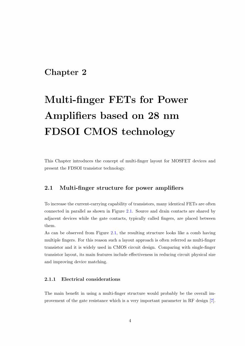
To increase the current-carrying capability of transistors, many identical FETs are often
connected in parallel as shown in Figure 2.1. Source and drain contacts are shared by
adjacent devices while the gate contacts, typically called fingers, are placed between
them.
As can be observed from Figure 2.1, the resulting structure looks like a comb having
multiple fingers. For this reason such a layout approach is often referred as multi-finger
transistor and it is widely used in CMOS circuit design. Comparing with single-finger
transistor layout, its main features include effectiveness in reducing circuit physical size
and improving device matching.
2.1.1 Electrical considerations
The main benefit in using a multi-finger structure would probably be the overall im-
provement of the gate resistance which is a very important parameter in RF design [7].
4

Chapter 2. Multi-fingers Power Amplifiers based on 28FDSOI technology 5
Figure 2.1: A typical layout of a multi-finger FET [1]
Generally a typical requirement is that:
Rg <<1
2πf0Cox
where Rg is the contribution of the polysilicon gate to the overall gate resistance, f0 is
the RF frequency and Cox is the oxide capacitance.
As depicted in Figure 2.1, a typical layout consists of drain and source directly connected
to the upper metal levels but the polysilicon gate contact is generally routed outside
the active area and then connected to a metal level. Therefore the gate resistance
contribution given by the polysilicon gate can be expressed as:
Rg = R′polyW
where R′poly is the polysilicon gate resistance per unit length and W is the gate width.
It is apparent that in a stand-alone transistor the current-carrying capability would be
strongly limited because of the limitation on the maximum transistor width W affecting
the gate resistance. Conversely a multi-finger geometry leads to very high electrical
aspect ratio that would not be feasible just by using one simple transistor since each
finger is now much shorter leading therefore to an acceptable finger gate resistance and
a desired high electrical aspect ratio:
W
L= N
WF
L

Chapter 2. Multi-fingers Power Amplifiers based on 28FDSOI technology 6
where W is the electrical transistor total width, L is the channel length and WF is the
finger electrical width.
Given a desired total aspect ratio WL , it is worth noticing that the total gate resistance
in a multi-finger structure is N2 lower than in a stand-alone device. In the former case
the N fingers are N times shorter than the stand-alone device and, in addition, their
electrical resistances are in parallel which means that the resulting overall resistance is
the finger gate resistance decreased by a factor N.
2.1.2 Thermal consideration
From a thermal point of view, a multi-finger structure has worse performance than a
stand-alone transistor because of thermal interactions between adjacent fingers leading
to an enhanced self-heating effect. Basically each finger is heated up by the neighboring
fingers because of the lateral heat spreading. Depending on the distance between fingers
(pitch) this phenomenon can be more or less strong.
Figure 2.2: Device thermal resistance versus number of fingers for (squares) FD 25-nmSOI MOSFETs and different packing densities.[2]
For this reason a non uniform temperature distribution is expected along the multi-
finger FET, with highly localized temperature gradients in the channel region. The
outer fingers in such a structure are expected to be the coolest while the ones in the
middle the hottest. Therefore the multi-finger FET junction temperature has to be
defined as the peak temperature inside the device.

Chapter 2. Multi-fingers Power Amplifiers based on 28FDSOI technology 7
2.2 28nm FD-SOI CMOS technology
A multi-finger MOSFET power amplifier for RF application has to be designed by using
the 28FDSOI CMOS technology provided by STMicroelectronics. There are several
available transistor’s choices which can be used. Only two of them have been chosen,
i.e. EGLVT and LVT devices, because they have been considered the most suitable
for power design. It is therefore necessary to introduce their geometrical properties,
materials and the metal stack structure as well as the electrical differences between
them.
2.2.1 Transistor’s geometry and materials
All the devices are placed on an SOI wafer 150µm thick (tsub = 150µm). The gate oxide
thickness tox and the minimum channel length Lmin depend on the specific device one
may want to use. It should be pointed out that tox is an equivalent oxide thickness
refering to an equivalent silicon dioxide layer having that thickness. The gate oxide is
indeed made with thicker layers of high-k dielectrics in order to reduce leakage currents
(because of the thicker layers) and at the same time to improve the gate electric control
on the channel of electrons(because of the high-k dielectric). The transistor’s geometry
is schematically depicted in the following pictures:
Figure 2.3: 28FDSOI transistor geometrical structure. (Courtesy STMicroelectron-ics)
In the present work, two different devices have been chosen, that is EGLVT (Extended
Gate Low threshold) and LVT (Low threshold) transistors. The following table summa-
rizes the main differences between them:

Chapter 2. Multi-fingers Power Amplifiers based on 28FDSOI technology 8
EGLVT LVT
Lmin 150nm 28nm
tox 2.8nm 1.8nm
Nominal voltage 1.8V 1.0V
Nominal pitch 290nm 130, 245, 260 nm
Table 2.1: EGLVT and LVT differences
The pitch has been defined as the distance between two adjacent devices in a multi-finger
structure, calculated from the middle of a finger to the middle of the adjacent one as
depicted in Figure 2.4:
Figure 2.4: Geometrical parameters in a multi-finger FET [3]
It should be pointed out that this parameter is generally arbitrary. However the 28FD-
SOI design kit provides a so called parametric-cell tool (P-CELL) which allows only the
pitch choices mentioned in Table 2.1 and consequently limits the maximum width of the
first level of metal routed between adjacent gates (the standard value is Wm = 50nm).
The use of a P-CELL is very convenient at the layout design level because it automaticaly
produces a layout for transistors which is very convenient for layout designers. Basically
with the P-CELL it is possible to quickly assign several transistor properties such as the
transistor dimensions, i.e. W and L, and the number of gate fingers. In addition one
may want to split the total finger width into several segments (y-gate split) if a matrix of
devices is desired. In this way the process of drawing transistors, at least up to the first
level of metal, is very quick which explains the adoption of the stardard pitch choices in
the present work.

Chapter 2. Multi-fingers Power Amplifiers based on 28FDSOI technology 9
2.2.2 Metal stack
28FDSOI metal stack uses copper metallization consisting of 10 metal levels. The metal
stack structure is schematically depicted in the following picture:
Figure 2.5: Schematic representation of the interconnection layer
The first 6 levels are thin and have ultra-low k dielectric. Then there are two medium
thickness layers having ultra-low k dielectric, while the remaining two levels are thick
and have TEOS/FTEOS dielectric. There is an aluminum cap as last metal level. It is
worth noticing the remarkable benefits introduced by the ultra-low k dielectrics in order
to reduce as much as possible the parasitic capacitances due to the interconnections.

Chapter 3
Heat transfer in nanoscale
semiconductor devices
In physics and chemistry, heat is defined as the energy trasferred from one system (or a
region of space) to another because of a temperature difference between them [8]. When
heat is transferred, a net flux of energy from the hotter system to the colder one will
result until thermal equilibrium is reached, that is, the situation when the temperatures
of the two systems are equal and the net flux of energy is zero.
There are three fundamental ways wherewith heat can be exchanged [9]:
• Conduction: the energy is transferred across a stationary medium, i.e. a medium,
either solid or fluid, whose properties do not change over time.
• Convection: the energy is transferred between an object and a fluid in motion
• Radiation: the energy is transferred by means of the emission or absorption of
electromagnetic radiation.
In electronic circuits, heat transfer via conduction is the dominant mechanism at the
device level. Such a mechanism is described by the well known Fourier’s law, presented
in 3.1
3.1 Heat conduction
Conduction is a mode of heat transfer between two regions at two different temperatures
within a solid, liquid or gas medium or between different media which are in physical
10

Chapter 3. Heat transfer in nanoscale semiconductor devices 11
contact with each other. The physical process of heat conduction can be defined as an
atomic or molecular activity that transfers thermal energy from a region with higher
temperature to a region with lower temperature. There are different conduction mech-
anisms depending on the structure of the matter. In solids, heat conduction is due to
a combination of lattice vibrational waves (or phonons) and diffusion and collisions of
free electrons. Heat conduction in liquids or gases is due to the random motion and
interaction of the molecules. [8]
3.1.1 Fourier’s Law
In 1822, baron Jean Baptist Joseph Fourier observed that:
the heat flux resulting from thermal conduction is proportional to the magni-
tude of the temperature gradient and opposite to it in sign.
This simple empirical observation has the name of Fourier’s law and can be expressed
mathematically as follows:
q = −k∇T (3.1)
where q is the heat flux, T is the temperature and k is the material thermal conductivity
matrix. It should be pointed out that k always varies with temperature and may vary
with orientation in case of anisotropic material, or space in case of non-uniform materials
or with size, as will be discussed in the next sections [9].
Equation 3.1 is the differential form of Fourier’s law and has an impressive analogy
with Ohm’s law in three dimensions:
j = −σ∇V
where j is the flux of electrical charge (or current density), σ is the electrical conductivity
and V is the electric potential. Therefore, by comparing Ohm’s law and Fourier’s law
one notices that current density is the analogous of heat flux as well as potential gradient
is the analogous of temperature gradient.
This analogy makes the life much easier for electrical engineers who want to study and
analyze the thermal behaviour of electronic devices and systems.
A possible way to understand the benefits of this analogy is the study of the thermal
behaviour of a rod with length L and cross-sectional area A. Assuming that the ends
of such a rod are kept at two different temperatures T1 and T2, one may wonder how
much the heat flux is.

Chapter 3. Heat transfer in nanoscale semiconductor devices 12
From an electrical perspective the problem is very simple because it consists of a simple
rod having a voltage difference ∆V across its ends. The current flowing through it will
be:
I =∆V
R
where R = LσA is the electrical resistance of the rod.
Therefore the current density is simply j = IA = σ∆V
L
Now, since the mathematical forms of Ohm’s law and Fourier’s law are exactly the same,
it is possible to state that the heat flux in the rod is:
q = k∆T
L
It is quite spontaneous to introduce the concept of thermal resistance of the rod as the
ratio between the temperature difference between its ends and the amount of heat Q
flowing per unit time through its cross-sectional area A:
Rrodth =
∆T
Q=
∆T
qA= ∆T
L
kA∆T=
L
kA(3.2)
As for electrical resistance, thermal resistance depends only on the geometrical and
material properties of the rod.
The reader may have observed that the use of Fourier’s law is limited to steady-state
analysis, that is, when thermal transients are completed. However it is well known from
every day experience that heating up a pot of water takes a certain amount of time. More
generally the amount of heat required to heat up an object up to a desired temperature
depends both on the volume and the material wherewith the object is made. This is
actually a property of every body and is called heat capacity:
∆E = C∆T
where ∆E is the addictional energy stored in a body after its temperature has been
increased by ∆T. Observe that the dynamic behaviour of thermal processes comes out
by making the first derivative of the previous equation respect to the time:
∂E
∂t= C
∂T
∂t
This simple example points out that thermal systems can quite often be converted into
thermal circuits and studied very quickly with the help of the electric circuits theory.

Chapter 3. Heat transfer in nanoscale semiconductor devices 13
The thermal-to-electric conversion criteria are summarized in Table 3.1:
Electrical Thermal
Voltage TemperatureCurrent Heat fluxElectrical conductivity Thermal conductivityCapaticance Heat capacity
Table 3.1: Electric-to-thermal conversion table
3.1.2 The Heat equation
Sometimes thermal systems are too complex to be easily converted into simple thermal
circuits and a more general method is required in order to study their behaviour and
face thermal design issues.
For the sake of ease let’s consider again the rod described in the previous section. Let’s
consider a slice of rod at x, having an elemental thickness dx. The outgoing amount of
heat Aq(x+ dx, t) results from the following contributions:
• The incoming amount of heat Aq(x, t)
• A possible heat source inside the slice H′(x, t)Adx
• The amount of heat that is been using over time to heat up the slice Cs∂T∂t Adx
(Cs is the slice heat capacity per unit volume)
Figure 3.1: Heat flux in an elemental part of a rod
Aq(x+ dx, t) = Aq(x, t) +H′(x, t)Adx− Cs
∂T
∂tAdx
By dividing both sides of the previous equation by dx and exploiting the definition of
derivative it follows that:∂q(x, t)
∂x= H
′(x, t)− Cs
∂T
∂t

Chapter 3. Heat transfer in nanoscale semiconductor devices 14
According to Fourier’s law q = −k ∂T∂x . Therefore:
Cs∂T
∂t=
∂
∂xk∂T
∂x+H
′(x, t) (3.3)
This is the one-dimensional Heat Equation and its solution gives the temperature dis-
tribution over space and time. The above equation can be generalized for the three-
dimensional case by substituting the partial derivative respect to x with the gradient
operator:
Cs∂T
∂t= ∇(ks∇T ) +H(r, t) (3.4)
where Cs and ks are the heat capacity per unit volume and the thermal conductivity
matrix, respectively, and H(r, t) represents the heat-generation rate per unit volume
in presence of an external heat source. Analytical solutions of such an equation are
difficult to find for complex geometries such as transistors, or more generally, integrated
circuits. For this reason ”finite element method” (FEM) is the only practical way that
lets thermal engineers study and design very complex thermal systems.
3.2 Heat conduction in nanoscale semiconductor devices
It is widely known that the thermal energy is transmitted within solid materials by a
combination of lattice vibrational waves (phonons) and diffusion and collisions of free
electrons. Also, it has been shown that the electron contribution is dominant among
the heat transport carriers in metals. However, for dielectrics and semiconductors it has
been estimated that the contribution given by electrons is around 1% even in the case
of very large concentrations and it is therefore negligible [2]. Basically a temperature
gradient in a semiconductor implies a gradient in the concentration of phonons. Heat
transport in such a situation can be still modeled by the heat equation 3.4 provided that
a proper thermal conductivity value is adopted. [2].
The phonon thermal conductivity can be derived from the kinetic theory of gases [10]:
kS =1
3CSvΛS (3.5)
where CS is the material heat capacity per unit volume, v is the average phonon velocity
and ΛS is the mean free path of a phonon between collisions.

Chapter 3. Heat transfer in nanoscale semiconductor devices 15
Another model has been suggested by Holland [4], in order to separately account for
the conduction of heat by longitudinal and transverse phonon modes, that is the three
polarization modes of the lattice vibrational waves:
k = kT + kTU + kL
where kT , kTU , kL are the transverses and longitudinal mode contributions to the thermal
conductivity.
The general expression for the phonon thermal conductivity provided by such a model
is rather complicated but can be drastically simplified at high temperatures, that is,
around 300 K:
kHT ≈ kTU + kL
where kTU ≈ 23CTUvTUΛTU and kL ≈ 1
3CLvLΛL. Therefore high temperature thermal
conductivity results:
kHT =2
3CTUvTUΛTU +
1
3CLvLΛL (3.6)
Whatever the adopted model is, it should be pointed out that for bulk undoped semi-
conductors, phonon mean free path is typically of the order of few hundreds of nm at
300K. In nanoscale devices the dimensions are of the order, or even smaller, than the
phonon mean free path in the bulk case. For this reason a reduction in the semiconductor
thermal conductivity is expected because of subcontinuum transport effects [2].
3.2.1 Enhanced scattering of phonons
Thermal conductivity in thin films can be drastically reduced with respect to bulk values
because of the enhanced scattering of phonons by the film boundaries and doping.
Materials having a crystal or polycrystal structure
The effect of boundary scattering can be accounted for by solving the Boltzmann trans-
port equation for energy carrier scattering at the film interfaces. In this way a boundary
scattering function F (χ = dsΛS−bulk
), where df is the film thickness and ΛS−bulk is the
phonon mean free path for a bulk undoped semiconductor, is obtained so that the overall
scattering whithin the thin film is [4]:
ΛS−film = ΛS−bulkF (χ).
However such a scattering function is rather complicated and an approximate function
that still describes properly the phenomenon is desirable. The authors in [4] and [11]

Chapter 3. Heat transfer in nanoscale semiconductor devices 16
showed that a good approximation could be:
F (χ)approx =
[1 +
B
χ
]−1
(3.7)
Basically this approximation assumes that boundary effects cause an addictional scat-
tering process having mean free path ΛS = Bdf where B is a proper constant (B = 1
in [11], B = 38π in [4]) and df is the film thickness.
The doping on the other hand enhances phonon scattering because of the introduction of
impurities and induced strain in the lattice. These two effects cause an overall additional
scattering process having a mean free path Λ−1IS . A possible mathematical derivation of
Λ−1IS has been proposed in [4].
Whether one uses the equation 3.5 or 3.6 the averaged mean free path can be calculated
using Mathiessen’s rule:
Λ−1S = Λ−1
S−bulk + Λ−1BS + Λ−1
IS
Experimental data of thermal conductivity in ultrathin silicon layers are shown in the
Figures 3.2 and 3.3, reported in [4], where the authors have proposed a model for the
size (equation 3.7) and doping enhanced scattering on thermal conductivity based on
Holland’s model.
Figure 3.2: On the left: room-temperature thermal conductivity data for siliconfilm layers as a function of thickness [4]. On the right: thermal conductivity versus
temperature in thin silicon layers calculated according to the models in [4] ([2])
It is worth mentioning how the thermal conductivity of Silicon dramatically decreases
as the film thickness goes below the µm range and for very high doping levels.
All the considerations that have been made so far can be extended to the case of poly-
crystals, such as polysilicon [12] [13]. In this case equations 3.5 and 3.6 are still valid
and the phonon mean free path can be evaluated by using Mathiessen’s rule provided

Chapter 3. Heat transfer in nanoscale semiconductor devices 17
Figure 3.3: Variation of thermal conductivity with doping concentration near roomtemperature. [4]
that the film thickness df is substituted with the average grain size of the polycrystal
dG.
Materials having an amorphous structure
In amorphous materials the phonon mean free path is determined by the degree of
disorder, specific for that material. Such a value should be reasonably close to the
average spacing a between atoms. When in equation 3.5 ΛS = a, the minimum thermal
conductivity of the amorphous solid is indeed obtained. It is worth mentioning that no
material has been found where the thermal conductivity near room temperature falls
significantly below this value [5]. Therefore phonon scattering in amorphous materials
is limited by the degree of disorder, or said in other words, other scattering processes,
such as boundary scattering, are of little practical importance in amorphous materials
[14], unless ultra-thin films are considered (of the order of 3.5 nm for SiO2 [5]).
Figure 3.4: Intrinsic (internal) thermal conductivity of the SiO2 film versus its thick-ness [5]

Chapter 3. Heat transfer in nanoscale semiconductor devices 18
3.2.2 Interface thermal resistance
The interface between two films can be seen as a highly porous layer, that is, a series
of anisotropic micro-voids oriented parallel with the plane of the films located at the
interface. This can produce a significant density deficit, which in turn can reduce the
heat transport through the interface [5]. For this reason the interface between two films
can be described with a thermal resistance per unit surface. Typical values are of the
order of 10−8m2KW−1 depending on the fabrication technique [5] [15]
The presence of interface thermal resistance may strongly affect the measurements when
extracting thermal conductivities for very thin films. Consider the following expression:
R′th
m= R′
thint
+R′th
f
where R′th
m, R′th
int and R′th
f are the measured thermal resistance, interface thermal
resistance and film thermal resistance per unit surface, respectively.
The measured thermal resistance per unit surface of the film can be expressed as:
R′th
m=
tfkext
where tf and kext are the film thickness and extracted thermal conductivity, respectively.
On the other side, the actual film thermal resistance per unit surface is:
R′th
f=
tfkf
Therefore the extracted thermal conductivity is:
kext =
(R′
thint
tf+
1
kf
)−1
It is therefore apparent that for very thin films the effects of interface thermal resistance
strongly affects the extracted thermal conductivity value.
For many years silicon dioxide thermal properties have been studied in order to predict
thermal conductivity as the film thickness scales down. Very low values compared to the
bulk case have been measured. The measured value was not the actual SiO2 thermal
conductivity because the presence of non negligible interface thermal resistances. It has
actually been shown in [5] [15] that its value is approximately the same as the bulk
value.

Chapter 3. Heat transfer in nanoscale semiconductor devices 19
Figure 3.5: Measured thermal conductivity versus the thickness of the SiO2 layer [5]
This result highlights the importance of considering interface thermal resistance as an
important effect in nanoscale devices, but, moreover, it confirms that amorphous mate-
rials, like silicon dioxide, keep the same thermal conductivity even for very thin films.
3.2.3 Heat generation in a nanoscale MOSFET device
Current flow between the source and drain results in resistive heating where the electrical
resistance is dominated by the gate region. It is there where most of the heat generation
occurs, more specifically under the depletion region created by the gate.
Heat generation in semiconductors occurs through the emission of phonons by carriers
heated by an electric field. The heating rate per unit volume in a MOSFET is tradi-
tionally calculated as the scalar product of the electric field and current-density vectors
J · F . Unfortunately this approach fails in taking into account nonlocal characteristics
of carrier heating and phonon emission when the channel length approaches the phonon
mean free path [2]. In fact, according to this model, the heat-generation region is located
inside the channel region and the heat-generation rate increases monotonically as the
electric field approaches its maximum value, that is, at the drain junction. However for
nanoscale MOSFETs the channel length is of the order of the mean free path for phonon
scattering and, for this reason, each carrier may suffer few scattering events, or even not
scattering at all, within the channel region. Conversely most of the heating process may
take place inside the drain.
Monte-Carlo simulations conducted by Pop et alii [6] confirmed this physical observation
and predicted a heat-generation peak located inside the drain junction and having a lower
value than expected by using the traditional method.

Chapter 3. Heat transfer in nanoscale semiconductor devices 20
Figure 3.6: Heat generation in MOSFET devices with channel lengths L =20 and 100nm. Solid lines are results of MC simulations, dashed lines are from Medici performedby the authors. Dotted lines represent the optical (upper) and acoustic (lower) phonon
generation rates given by the MC simulation.[6]
From Figure 4.14 it is worth noticing how the entire heat generation region is mostly
displaced towards the channel-to-drain junction how such an effect is stronger in shorter
devices.
However in the present work the conventional ”JF” model for Joule heating has been
adopted. In fact, in spite of its inherent local approximation, such a model is still largely
adopted in consideration of the ease of implementation in the frame of device simulators
[2]

Chapter 4
Thermal modeling for finite
element analysis
As seen in Chapter 3, Heat Equation 3.4 is the most complete way to describe the tem-
perature distribution over space and time in a thermal system. Unfortunately, the study
of temperature distribution of electronic devices leads to a very complex system of math-
ematical equations to be combined with the heat equation. Therefore it is practically
impossible to solve analytically such an equation and the finite element method (FEM)
has to be considered as the only practical way to face this problem. This approach works
by dividing the geometry into a great number of small subregions, all having their own
set of equations, followed by recombining all of them into a global system for the final
calculation. FEM is nowadays implemented in finite element analysis softwares, that is,
computational tools for performing engineering analysis. In the present work, COMSOL
Multiphysics 4.3 has been used as the simulation tool.
4.1 Introduction to COMSOL Multiphysics
COMSOL Multiphysics is a finite element analysis, solver and simulation software for
various physics and engineering applications, especially coupled phenomena, or multi-
physics.
The COMSOL Multiphysics simulation environment facilitates all the steps in the mod-
eling process such as defining geometries, meshing, specifying the physics, solving, and
then visualizing results. Model set-up is quick, thanks to a number of predefined physics
21

Chapter 4. Thermal modeling for finite element analysis 22
interfaces for applications ranging from fluid flow and heat transfer to structural me-
chanics and electrostatics. Material properties, source terms, and boundary conditions
can all be spatially varying, time-dependent, or functions of the dependent variables.
Geometries definition
Geometries can be created with the help of a proper drawing environment, both by
simply drawing by hands the desired shapes or by adding predefined objects whose
parameters can be properly defined. Of course, import of geometries is supported and
should be considered in case of very complex geometries since the drawing environment
is not as powerful as other CAD softwares.
Materials definition
A geometry itself is only a region of space without any physical meaning. For this reason
every geometrical pattern has to be described with proper physical quantities. E.g., in
thermal simulations each geometry has to be described with a specific heat capacity and
a thermal conductivity. In COMSOL this can be done very quickly thanks to the library
“Materials” where a wide variety of materials is provided. Of course new materials can
be defined by modifying an existing one or just by creating a new one.
Definition of the physics to be used
The problem has to be described with a specific partial differential equation (PDE) hav-
ing proper boundary conditions, external sources etc. This can be accomplished thanks
to the ”Physics” library that lets the user add the desired ”physics” (Heat transfer,
Mechanics, etc). Once the physics has been choosen, boundary conditions and external
sources can be defined very quickly.
Mesh definition
The finite element method requires the overall geometry to be divided into smaller
regions. COMSOL provides a mesh generator that can be software-defined or user-
defined. Several meshing techniques are available.
Study definition
The user may want to perform a steady-state simulation instead of a time-dependent
one. Or he may want to set-up a simulaton plan, where, e.g., one or more parameter is
varied at each step. This can be easily accomplished in COMSOL by adding a proper
study definition.
Results
Results are displayed automatically when a simulation is completed in the form of color
maps. It is possible to extract and export data from specific regions of the geometry.

Chapter 4. Thermal modeling for finite element analysis 23
4.2 General considerations
The instantaneous power dissipated by a RF power amplifier is a time-dependent phys-
ical quantity since it is given by the product of the current flowing through the active
components, i.e. transistors, and the voltage across them. For the sake of ease let’s
assume that the resulting power can be expressed as follows:
Pdiss(t) = i(t)v(t) = PDC + PAC cos(2πf0t+ ϕ)
where PDC and PAC are, respectively, its DC and AC value, f0 is the frequency and ϕ
is a phase shift.
According to the analogy between Ohm’s law and Fourier’s law each thermal system
can be modeled with a first-order thermal circuit:
Figure 4.1: First order equivalent thermal circuit of a thermal system
Such a circuit is a simple RC filter where the electrical quantities have been converted
into thermal quantities according to Chapter 2. If the output is the temperature T , it
is well known from the electric circuits theory that such a circuit behaves as a low pass
filter and therefore it cuts off the spectral components above a characteristic frequency
f∗ = 12πRthCth
which is typically around few tens of KHz in thermal systems.
Since the frequency range involved in mobile phone applications is of the order of GHz,
which is much greater than f∗, the thermal system cuts off the AC power component
and the resulting output temperature is determined by the DC component PDC .
For this reason steady-state simulations have been performed in the present work, con-
sidering hence only the average power PDC dissipated by the active component.

Chapter 4. Thermal modeling for finite element analysis 24
4.3 Geometry and boundary conditions
For the sake of ease let’s start just by considering a very simple and conceptual geomet-
rical model for a multi-finger FET. Such a geometry consists of a periodic array of N
transistors placed on a SOI substrate. Since these transistors are electrically connected,
an interconnect layer has to be considered too. In such a scenario the temperature dis-
tribution along the device is not uniform because of cross heating between neighboring
fingers. In fact the outer fingers are the coolest, while the ones in the middle are the
hottest. Therefore accurate thermal simulations are required in order to evaluate the
temperature peak. The device geometry can be drawn according to Chapter 2. However,
simulating an entire multi-fingers FET consisting of tens or hundreds of fingers, would
require a huge amount of resources in terms of CPU and memory usage as well as time,
if any semplification on the geometry were not considered.
For this purpose it should be observed that in a real case, e.g. for power amplifier
design, a very high number of fingers is required because of the need to sustain very high
currents. From a thermal point of view, it has been shown that only the neighboring
fingers positioned within one substrate height contribute to cross heating [3]. As a
consequence of that, an infinite number of fingers can be assumed in any practical case
and a zero net heat flux is expected between two neighboring fingers situated in the
middle of the structure. This is equivalent to assigning adiabatic surfaces between each
finger and the next, as indicated by the dashed lines in Fig. 4.2.
Figure 4.2: Cross section of an FET composed of multiple gate fingers.
Thus, the geometrical model can be dramatically simplified by considering only a single-
finger region and assigning adiabatic boundary conditions on its lateral surfaces [3].

Chapter 4. Thermal modeling for finite element analysis 25
Figure 4.3: Extraction of a finger from the multi-finger structure. The red linehighlights the adiabatic boundary condition on the lateral surfaces of the finger.
Observe that a zero flow surface implies a mirroring of all the geometry in the simulation
region at this surface resulting in a situation with a periodic array of virtual device
structures being simulated. The spacing between the devices in this array is determined
by the size of the simulation region [16]. This boundary condition is therefore very
usefull for simulating devices arranged in a periodic structure.
Figure 4.4: Effect of adiabatic boundary condition on the lateral surfaces of theextracted finger. A matrix of virtual devices is generated.
It is worth noticing that such a boundary condition creates a matrix of virtual devices
which does not describe the desired situation since the virtual array is wanted only along
the source − to − drain direction (vertical direction in Figure 4.4). The effect of the
unwanted virtual devices can be neglected provided that a heat spreading region on the
order of the die thickness is placed next to the active area. In this way the virtual
devices are far away from the real device and the thermal interaction between them can
be therefore neglected (Figure 4.5).

Chapter 4. Thermal modeling for finite element analysis 26
Figure 4.5: Effect of the heat spreading region (yellow): the elements of the virtualarray in the horizontal direction are more spaced and therefore their influcence on each
other is negligible.
Observe that a further simplification of the geometry have been made, by considering
only half-geometry, that is the geometry obtained by cutting in half the above mentioned
geometry, provided that an adiabatic boundary condition is assigned on the cutting sur-
face. It should be pointed out that the last simplification on the simulated geometry, i.e.
half-finger geometry, lead to a different virtual devices matrix. The difference consists of
perfect symmetry in the interconnections which is not true in the actual layout. However
this simplification is expected to not change in an appreciable way the simulation results
since the interconnects are assumed to play just a negligible role in the dissipation of
the heat generated in a finger.
Interconnect thermal modeling is actually a really difficult task to deal with since the
real interconnect structure is not known a priori. There may be several possible way to
face this issue:
1. Adiabatic boundary condition on the source, drain and gate surfaces. Interconnect
layer completely neglected
2. Interconnect layer modeled simply as an oxide layer, neglecting the metallizations
3. Source,drain and gate surfaces connected to an isothermal boundary condition
through proper lumped thermal resistances, and an oxide layer is assumed as
interconnect layer
4. Source, drain and gate connected to a typical interconnect structure which is
routed up to the first level of metallization. An adiabatic boundary condition
is then assigned on the top surface of the interconnect layer. The dielectric in the
interconnect is SiO2
Case 1. would be an extreme unrealistic worst case since no heat flux through the in-
terconnects is allowed.
Case 2. would be a more realistic case since heat flux through the interconnect layer is

Chapter 4. Thermal modeling for finite element analysis 27
allowed. However the enhancement on thermal performance produced by the metalliza-
tions is neglected.
Case 3. would be a very good realistic case if only the lumped resistance values and the
temperature for the isothermal boundary condition were known.
Case 4. is probably the best way to take into account of the heat flux through the
interconnect layer and the thermal performance enhancement due to metallizations.
Of course Case 3. would be the best choice but it needs some parameters’ values which
are unknown. Therefore Case 4. has been adopted in the present work.
The layout structure is the one shown in Figure 4.3 where source and drain are routed
up to the first level of metallization. It should be pointed out that it still represents a
worst case scenario but it is, probably, more realistic than cases 1. and 2. Furthermore
it is important to highlight that a slightly simplified geometry has been adopted instead
of the one shown in Chapter 2. Figure 4.6 shows the cross sectional and the top view
respectively of the resulting simplified transistor geometry.
Figure 4.6: Simplified transistor geometry in COMSOL
As the reader may have noticed the conformal nitride geometry has been slightly modi-
fied as well as the silicon-metal 1 contacts which have been modeled as a single contact
made of copper. Another simplification is the assumption that the dielectric layers be-
tween metals are made of silicon dioxide. These simplifications should not change in
a perceptible way the overall thermal behaviour of the simulated devices since thermal
dissipation occurs mostly through the substrate (as will be discussed in the following
chapters).

Chapter 4. Thermal modeling for finite element analysis 28
The remaining boundary condition to be defined is on the bottom surface of the sub-
strate. The device under study is basically a slice of a silicon die, which is inside a
package soldered on a printed circuit board (PCB). The latter can have a heat sink that
helps heat dissipation into the air. This situation can be represented schematically by
an equivalent thermal circuit, exploiting the analogies between Ohm’s law and Fourier’s
law presented in Chapter 3. From Figure 4.7 it is possible to notice that:
Figure 4.7: Packaging equivalent thermal circuit
• Pdiss: is the power dissipated by the device. It is the analogous of the electric
current
• Rθ−JC : is the junction-to-case thermal resistance
• Rθ−CH : is the case-to-heat sink thermal resistance
• Rθ−HA: is the heat sink-to-air thermal resistance.
The package thermal performances are not known a priori. Therefore a possible way to
deal with that is to use a typical maximum case temperature (in order to deal with the
worst case), specific for the desired application. In the present work the maximum case
temperature is taken as 85 C which is representative of the condition at the upper end
of the IS98 standard that specifies an external ambient of −30 C to +60 C outside of
the phone [17] An isothermal boundary condition at 85 C is therefore assigned on the
bottom surface of the substrate.

Chapter 4. Thermal modeling for finite element analysis 29
This approach makes possible to easily calculate the transistor thermal resistance as the
junction-to-case resistance:
Rθ−JC =Tjunction − Tcase
Pdiss
Figures 4.8 shows the resulting geometry accounting for the previous mentioned bound-
ary conditions:
Figure 4.8: Schematic representation of the simulated geometry (not in scale). Allthe surfaces of the parallelepiped are adiabatic except for the one on the bottom which
is isothermal.
4.4 Materials
Each element of the geometry has to be thermally defined in terms of thermal conduc-
tivity and heat capacity. This can be done very quickly in COMSOL by assigning each
geometry to a specific material, according to FDSOI28 technology described in Chapter
2. However the material thermal properties for most of the geometries have to be cor-
rected according to Chapter 3 because of size effects in nanoscale devices, that is thermal
conductivity degradation and interface thermal resistances. It should be observed that
addictional corrections have to be apported because of temperature effects.

Chapter 4. Thermal modeling for finite element analysis 30
4.4.1 Thermal conductivity degradation
Thermal conductivity values for Undoped Si are exptrapolated from Figure 4.9 from
Chapter 3 while thermal conductivity for SiO2, Si3N4 and Cu are assigned according to
[5, 15, 18, 19]. Silicon Nitride thermal conductivity has actually a quite high uncertainty
because other works reported values differing up to 50 % [18].
Figure 4.9: Room-temperature thermal conductivity prediction (left) and experimen-tal data (right) for silicon film layers as a function of thickness according to [4]
Thermal conductivity values for doped Si as well as for doped polysilicon are a bit
difficult to be extrapolated because the doping type and level is not known as well as
the grain size. However from Figure 4.10 it can be observed that whatever the doping
type and level is, thermal conductivity values for doped Si are approximately in the
range of 10 - 20 [Wm−1K−1] if the layer thickness is below 20nm.
Figure 4.10: Variation of thermal conductivity with doping concentration near roomtemperature. [4]
Considering that the doped regions are tdoped thick (confidential), that the level of doping
may be possibly very high, and since the worst case has to be considered a thermal
conductivity of 10 [Wm−1K−1] is the most appropriate choice for doped Si.

Chapter 4. Thermal modeling for finite element analysis 31
Doped polysilicon is even more problematic since neither the grain size nor the doping
level is known. Furthermore no experimental data is available for thicknesses below
200 nm. However if the tpoly thick (confidential) gate layer was a doped crystal, the
thermal conductivity would range from 18 to 45 [Wm−1K−1] approximately. Since the
doping level may be very high, the gate layer is actually a polycrystal with a grain size
smaller than the film thickness, and since the worst case has to be considered, a thermal
conductivity of 18 [Wm−1K−1] is chosen.
Temperature effects are accounted for considering an average thermal conductivity within
the temperature range 360 K - 400 K (85C− 125C). The upper limit is the maximum
junction temperature allowed in a transistor, according to STMicroelectronics FDSOI
technology manual, leading to a maximum error of 7 % for bulk Si thermal conductivity
(Figure 4.11, left). Temperature effects on thermal conductivity for very thin films are
not as strong as for bulk materials in the temperature range of interest, as can be seen
from Figure 4.11 (right), and thus they have been neglected.
Figure 4.11: Variation of thermal conductivity as a function of temperature for bulkSi (left [4]) and different thin films of Si (right [2]).
The resulting thermal conductivity values are summarized in Table 4.1:
Material Film thickness [nm] Thermal conductivity [Wm−1K−1]
Undoped Silicon Bulk 107Undoped Silicon 7 10Doped Silicon -confidential- 10Doped polysilicon -confidential- 18Silicon dioxide Bulk 1.38Silicon dioxide < 100 1.05Silicon Nitride -confidential- 2.1Copper Bulk 400
Table 4.1: Thermal conductivity values to be adopted in the finite element analysismodel.

Chapter 4. Thermal modeling for finite element analysis 32
4.4.2 Interface thermal resistances
According to Chapter 3, as the film thickness goes below the µm range size effects start to
be stronger and stronger. In this scenario, besides the thermal conductivity degradation
phenomenon analyzed in the previous section, interface thermal resistances play a very
important role. Several works have shown that interface thermal resistance per unit
surface is on the order of 10−8KW−1m2 depending on the fabrication technique [5, 15].
Since there are no ways to know exactly the value of such an interface resistance for
each interface, an indicative value of 10−8KW−1m2 has been used for the simulations in
the present work. In COMSOL this has been accomplished by adding a thin thermally
resistive layer having a dummy thickness, e.g 0.5nm, and having an equivalent thermal
conductivity:
keq =tintR′
int
= 0.05 Wm−1K−1
It should be pointed out that this is not an actual layer. It is simply a boundary condition
that has been defined at every interface between two different materials. Therefore
COMSOL will see this condition as a simple resistance per unit surface.
4.5 Mesh
Meshing is a very important step when a simulation has to be performed. It determines
both the accuracy-resolution of the simulation and the computational load. For this
reason a structured smart mesh has to be properly defined in order to minimize as
best as possible the accuracy-computational load product. When doing this task it is
fundamental to carefully analyze the geometry to be meshed. In the adoped geometry,
schematically represented in Figure 4.8, there are basically two regions: the active area
where half-finger of the device is, and a heat spreading region, necessary in order to avoid
undesired boundary effects. The reader may have noticed that such a structure has a
very high degree of redundancy along the y-direction. In fact, if the finger were infinitely
long every cross-section would have exactly the same temperature profile. Therefore in
the case of a finger having a finite width a low temperature gradient is expected along
y-direction. The only critical region would be the interface between the active area
and the heat-spreading region, where boundary effects have to be carefully taken into
account. A low degree of detail is thus required along the y-direction, with the exception
of the above mentioned critical region.
On the other hand, the transistor cross-section consists of many different regions having
a very high aspect ratio. For this reason a high degree of detail is required in this case.

Chapter 4. Thermal modeling for finite element analysis 33
Sweeping the mesh of the transistor cross-section through the y-direction could be a very
smart way for meshing the entire geometry, based on what has been observed so far. This
mechanism creates replicas of a desired 2-dimensional mesh along the sweeping direction,
e.g. y-axis. However swept meshing can be applied only for very nice geometries, i.e.
having the same cross-section along the sweeping direction. This is true for the whole
active region but not for the heat spreading region, according to Figure 4.4 because of
source, drain and gate routing and because of the absence of polysilicon, metallizations
and doped regions there. This problem can be handled by assigning to the heat spreading
region the same geometrical pattern of the active region provided that the polysilicon,
metallizations and epitaxial geometrical patterns are considered as dielectrics, which
keeps therefore the desired thermal properties there. It should be pointed out that
this operation neglects the presence of source, drain and gate routings inside the heat
spreading region. However thermal dissipation mostly occurs through the substrate in
the active region which makes this approximation quite reasonable.
Under the above mentioned simplifications it is possible to implement a swept mesh
along y-direction. The cross-sectional surface has been meshed by using a structured
triangular mesh consisting of a very high element density at the transistor level, where
the smallest regions are, and lower density of elements in the substrate and interconnect
layer regions.
Figure 4.12: Meshing structure on the EGLVT cross-sectional surface
The sweeping step, of course, has to be more dense nearby the above mentioned critical
region, but, on the other hand, it can be very coarse elsewhere. The mesh density is
smaller and smaller as the y-coordinate approaches the critical region, and for this reason
it is a function of y. A possible mathematical implementation for the mesh distribution
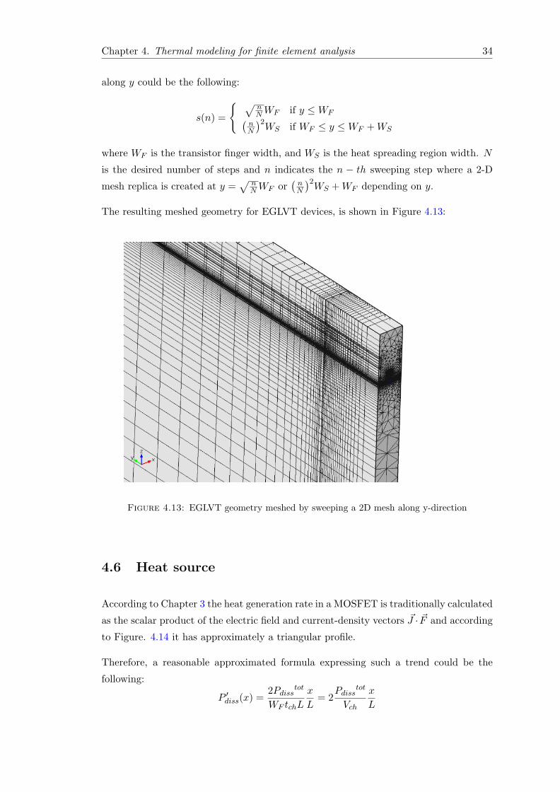
Chapter 4. Thermal modeling for finite element analysis 34
along y could be the following:
s(n) =
√nNWF if y ≤ WF(
nN
)2WS if WF ≤ y ≤ WF +WS
where WF is the transistor finger width, and WS is the heat spreading region width. N
is the desired number of steps and n indicates the n − th sweeping step where a 2-D
mesh replica is created at y =√
nNWF or
(nN
)2WS +WF depending on y.
The resulting meshed geometry for EGLVT devices, is shown in Figure 4.13:
Figure 4.13: EGLVT geometry meshed by sweeping a 2D mesh along y-direction
4.6 Heat source
According to Chapter 3 the heat generation rate in a MOSFET is traditionally calculated
as the scalar product of the electric field and current-density vectors J · F and according
to Figure. 4.14 it has approximately a triangular profile.
Therefore, a reasonable approximated formula expressing such a trend could be the
following:
P ′diss(x) =
2Pdisstot
WF tchL
x
L= 2
Pdisstot
Vch
x
L

Chapter 4. Thermal modeling for finite element analysis 35
Figure 4.14: Heat generation in a MOSFET device with channel length L = 100 nm.Dashed lines represents the heat-generation rate as a function of x according to theJoule Heating model.[6]. Source-to-channel and drain-to-channel junctions are at x = 0
and x = L respectively.
where P ′diss(x) is the heat generation rate per unit volume as a function of x, Pdiss
tot is
the total dissipated power, L, WF and tch are the channel length, width and thickness
respectively and Vch = WF tchL is the channel volume. Of course the channel region is
assumed to begin at x = 0. If the above formula is integrated over the entire channel
region Pdisstot is of course obtained. It is important to highlight that heat generation
takes place in the whole channel region, it being fully depleted.
Finally it is worth mentioning that several authors [3, 20, 21] adopted a much simpler
model for the heat generation region. They simply assumed a uniform heating rate along
the channel:
P ′diss =
Pdisstot
Vch
In the present work the Joule Heating model has been choosen since it is more accurate
and physically reasonable. Nevertheless a comparison between these two different models
will be presented in the following chapter in order to prove that a uniform power source
may cause a not neglibible underestimation of the junction temperature.
Chapter 5
Thermal simulations on LVT and
EGLVT devices
In this Chapter, thermal simulations on nanoscale multi-finger FDSOI MOSFET devices
have been performed in order to investigate their thermal behaviour with respect to the
geometrical parameters, i.e. finger width WF , gate length L and gate-to-gate spacing
(or pitch) p.
The simulations have been performed according to the finite element analysis model
realized in Chapter 4. In addition, a sensitivity analysis of the results with respect to
deviations of the adopted parameters in the simulation environment has been conducted
for each device. This approach is necessary in order to estimate the degree of accuracy
of the obtained results and, at the same time, understand which are the most critical
parameters, that is, the parameters one needs to know in a very accurate way.
5.1 General considerations
As mentioned in Chapter 4 simulations are performed assuming the bottom surface of the
substrate at a specific temperature, that is 85C. Since all the adopted parameters have
been chosen accounting for the temperature influence on them in the range 85C−125C,
a zero K isothermal boundary condition can be applied on the bottom of the substrate
at the simulation level. In fact the interest is only on the junction temperature increase
with respect to the case temperature, i.e. the junction-to-case temperature. In this way
the transistor thermal resistance of a single finger in the multi-finger structure can be
36

Chapter 5. Simulations of LVT and EGLVT devices 37
calculated according to Chapter 4 as:
R1Fth =
∆T
Pdiss=
Tj
P 1Fdiss
where Tj is the transistor junction temperature, extracted from the simulation results
when an arbitrary input power P 1Fdiss is assigned to each finger.
From the above formula it is apparent that the overall resistance of a N-finger MOSFET
is given by:
Rth−FET =∆T
P totdiss
=Tj
P totdiss
=Tj
NP 1Fdiss
=R1F
th
N
where P totdiss is the power dissipated by the N-finger MOSFET.
5.1.1 Width determination for the heat spreading region
As discussed in Chapter 4 the adopted boundary conditions create a matrix of virtual
devices which does not describe the desired situation. The virtual array is indeed wanted
only along the source− to− drain direction (vertical direction in Figure 5.1) and abso-
lutely not along the other one (horizontal direction):
Figure 5.1: Effect of the heat spreading region (yellow).
The effect of the unwanted virtual devices along the y-direction can be neglected pro-
vided that the heat spreading region width Ws is properly assigned. This value can be
determined by performing several simulations using different Ws and evaluating at each
step the temperature difference obtained between the present and the previous steps.
When such a difference starts to be less than, e.g, 1% of the junction temperature an
acceptable value for Ws is obtained.
Figure 5.2 shows the trend of the percentage error on the junction temperature obtained
by following the above strategy:
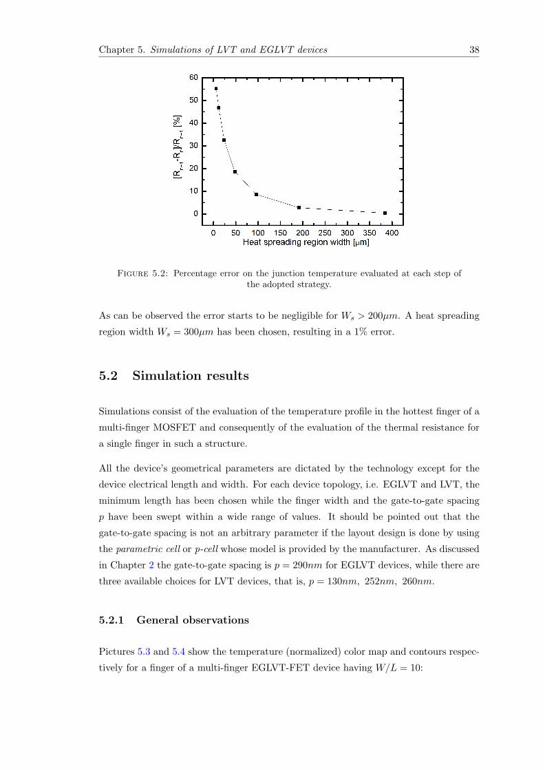
Chapter 5. Simulations of LVT and EGLVT devices 38
Figure 5.2: Percentage error on the junction temperature evaluated at each step ofthe adopted strategy.
As can be observed the error starts to be negligible for Ws > 200µm. A heat spreading
region width Ws = 300µm has been chosen, resulting in a 1% error.
5.2 Simulation results
Simulations consist of the evaluation of the temperature profile in the hottest finger of a
multi-finger MOSFET and consequently of the evaluation of the thermal resistance for
a single finger in such a structure.
All the device’s geometrical parameters are dictated by the technology except for the
device electrical length and width. For each device topology, i.e. EGLVT and LVT, the
minimum length has been chosen while the finger width and the gate-to-gate spacing
p have been swept within a wide range of values. It should be pointed out that the
gate-to-gate spacing is not an arbitrary parameter if the layout design is done by using
the parametric cell or p-cell whose model is provided by the manufacturer. As discussed
in Chapter 2 the gate-to-gate spacing is p = 290nm for EGLVT devices, while there are
three available choices for LVT devices, that is, p = 130nm, 252nm, 260nm.
5.2.1 General observations
Pictures 5.3 and 5.4 show the temperature (normalized) color map and contours respec-
tively for a finger of a multi-finger EGLVT-FET device having W/L = 10:

Chapter 5. Simulations of LVT and EGLVT devices 39
Figure 5.3: Temperature color map for a multi-finger EGLVT-FET in the channelregion area. The darkest areas are the hottests.
It is worth noticing how the temperature gradient is higher in the channel-buried oxide
region than elsewhere and that the temperature peak is not placed right in the middle
of the channel but, conversely, is shifted to the right. This is due to the adopted more
realistic JF Joule heating model for the heat source in the channel instead of the uniform
heat source used by other authors.
Figure 5.4: Temperature contours for a multi-finger EGLVT-FET in the channelregion area. The darkest surfaces are the hottests.

Chapter 5. Simulations of LVT and EGLVT devices 40
Observe also the role of the interconnects layer depicted in Figure 5.5:
Figure 5.5: Heat flux lines in the channel region of a multi-finger EGLVT-FET. Thearrows’ length is proportional to the logarithm of the flux intensity.
Flux lines are allowed to go upwards, but then they “turn back” and go towards the
substrate. The presence of metals enhances the above mentioned phenomenon which
is, however, not so important since the heat flux intensity is generally very low as can
be easily observed in the picture (the arrows are very short, or even point-like, in the
interconnect region).
Finally it is interesting to see how the heat spreads out through the substrate and the
heat spreading region (Figure 5.6).
Figure 5.6: Temperature contours for a multi-finger EGLVT-FET. Boundary effectsand head dissipation through the subtrate are highlighted.

Chapter 5. Simulations of LVT and EGLVT devices 41
As expected, the temperature is lower in the boundary region between the active region
and the heat spreading region. Observe how the temperature gradient between the
buried oxide and the substrate, represented by the distance between two isothermal
surfaces, is very low due to the high thermal conductivity of the silicon substrate.
5.2.2 EGLVT and LVT devices
In this subsection, the thermal resistance of a finger inside a multi-finger structure as a
function of the transistor finger width WF , pitch p and device topology is investigated.
Such trends have been obtained in COMSOL for EGLVT and LVT devices by sweeping
the finger width parameter as follows:
WF = Lmin2n
for n=0,...,8. In this way all the devices can be compared on the base of the aspect
ratio W/L = 2n. An indicative input power of 100µW and 20µW has been adopted for
EGLVT and LVT devices, respectively. The thermal resistance is therefore calculated
just by dividing the maximum temperature obtained from the simulation at each step
(the junction temperature) and the input power. It has to be pointed out that the results
provided by these simulations are of great interest in the design of a power amplifier.
By fitting or just by extrapolating the data of interest from the curves resulting from
thermal simulations it should be possible to understand which may be the best way to
design a PA in order to satisfy both thermal and RF requirements or to predict the
thermal behaviour of an existing FDSOI power amplifier.
Figure 5.7 shows the thermal resistance trend of one of the N fingers of EGLVT and
LVT devices as the finger width WF increases.
Figure 5.7: Thermal resistance as a function of the finger width for EGLVT (left)and LVT (right) devices.

Chapter 5. Simulations of LVT and EGLVT devices 42
As depicted in the picture the thermal resistance decreases as the finger width increases.
This is quite reasonable since the surface through which heat can spread and then flow
to the substrate is wider as the finger width increases. Similarly EGLVT device shows
better thermal performances because of a wider active area but also because of a larger
gate-to-gate spacing (290nm) compared to LVT devices. Actually the effect of the gate-
to-gate spacing is very important and it is higlighted in the picture on the right in Figure
5.7 where it can be observed how such an effect starts to be effective as the aspect ratio
is around 10. Gate-to-gate spacing or pitch is therefore a very important geometrical
parameter since it determines how much a finger is heated up by the neighboring fingers.
The lower the spacing is the stronger the cross heating effect will be.
If, e.g., an aspect ratioW/L = 10 is chosen and Pdiss = 100µW the junction temperature
will increase of 20C, 70C and 100C above the case temperature for EGLVT, LVT
(p=260nm) and LVT (p=130nm), respectively. The choice of the right device and
geometry could therefore reveal a fundamental aspect for a really cutting-edge thermal
design for power amplifiers.
5.2.3 Sensitivity analysis
In order to understand the credibility of the above results it is fundamental to perform a
sensitivity analysis of the results with respect to deviations of the adopted parameters.
This can be accomplished by varying of a desired percentage one or more parameters
per time and then evaluating the variation of the results with respect to a reference case.
Size effects and interface thermal resistances
First of all it is very interesting to observe what happens if the thermal conductivity
degradation when the films are very thin (size effects) and/or the presence of interface
thermal resistances (ITR) are neglected at all. The consequences of doing so are shown
in Figure 5.8 where the reference case for the thermal resistance value is when both
size effects and ITR are taken into account. As expected, the transistor finger thermal
resistance would be strongly underestimated if both size effects and interface thermal
resistance were neglected at all. The error is generally affected by the finger aspect ratio
W/L, the device type and the gate-to-gate spacing. In fact a high finger aspect ratio
means a wide active area which enhances heat conduction through the substrate. A
low gate-to-gate spacing enhances cross heating of neighboring fingers which blocks heat
flowing laterally and therefore, forces heat to flow through the substrate. Said in other
words, in both cases heat conduction through the substrate is enhanced and, conversely,
lateral heat conduction results weaker for high W/L and low gate-to-gate spacing.

Chapter 5. Simulations of LVT and EGLVT devices 43
Figure 5.8: Percentage error on the devices thermal resistance if size effects areneglected.
Under the above mentioned circumstances the influence of lateral heat conduction on the
overall heat dissipation becomes less important and the same goes for the uncertainty
on the parameters affecting it, i.e. size effects. The contribution given by the interface
thermal resistance, on the other side, is a bit harder to understand. For low aspect ratio
values the presence of ITR enhances lateral heat conduction and for this reason, if size
effects are taken into account, the error is lower than in the “neglect-all” case. For high
aspect ratio values, conversely, heat conduction through the substrate is enhanced and
therefore the error is reduced more and more as W/L is increased.
What it is important to highlight is that the error may be very high, i.e. up to −75%
and −85% for EGLVT and LVT devices respectively, if size effects and interface thermal
resistance were both neglected.
In the present work size effects and interface thermal resistance have been taken into
account in simulations. However the parameters describing such effects have a certain
degree of uncertainty because they have been extracted from graphs made by other
authors (thin film thermal conductivity) or have been estimated according to typical
measured values (interface thermal resistance). Given the absence of any available data
regarding the uncertainties on the parameter of interests, in this work it has been simply
assumed that the thermal conductivities and ITR values are characterized by a relative
standard deviation of 20% and 50% respectively.
Sensitivity to interface thermal resistance
Figure 5.9 shows the relative error on the thermal resistance when the interface thermal
resistance is varied around its value of 50%.
As can be seen the error is generally below 15% both for LVT and EGLVT devices. This
result shows that thermal resistance sensitivity to interface thermal resistance is pretty

Chapter 5. Simulations of LVT and EGLVT devices 44
Figure 5.9: Percentage error on the devices thermal resistance if interface thermalresistances are varied of +/− 50%.
low. Therefore even if a very uncertain value for ITR is adopted, a low error on the
simulated thermal resistance is expected.
Sensitivity to thin film thermal conductivity
Figure 5.10 shows the relative error on the thermal resistance when the thin film thermal
conductivities are varied around their value of 20%. If W/L > 10 (usually this is true
Figure 5.10: Percentage error on the devices thermal resistance if thin films thermalconductivities are varied of +/− 20%.
in a power amplifier) the error is below 10%. However such an error is pitch-dependent
as can be easily observed from the LVT graph. Basically higher pitches enhance lateral
heat conduction which depends on the thin films thermal conductivities. For this reason
uncertanties on such parameters propagate up to the thermal resistance leading to higher
errors. It is worth noticing that it is desirable to use the lowest gate-to-gate spacing
possible in order to minimize area. In this case the choice of, e.g., LVT (p=130nm)
would lead to a maximum error of 10% if W/L > 10.

Chapter 5. Simulations of LVT and EGLVT devices 45
Sensitivity to substrate thermal conductivity
Figure 5.11 shows the relative error on the thermal resistance if the substrate thermal
conductivity is varied around its value of 20%. From the picture, it can be seen that
Figure 5.11: Percentage error on the devices thermal resistance if substrate thermalconductivity is varied of +/− 20%.
the error on the thermal resistance is below 10% if W/L < 20 and W/L < 100 for
EGLVT and LVT devices respectively. This result is quite intuitive since as the aspect
ratio becomes higher and higher, heat conduction through the substrate (which strongly
depends on the substrate thermal conductivity) is more and more enhanced, becoming
the main factor affecting the overall thermal resistance. For this reason substrate thermal
conductivity is a very critical parameter and should be as precise as possible.
Sensitivity to the adopted power source model
Finally the following picture shows the error on the thermal resistance if a uniform heat
generating region is adopted instead of the joule heating model.
Figure 5.12: Percentage error on the devices thermal resistance if a uniform powersource is adopted instead of a linear profile.

Chapter 5. Simulations of LVT and EGLVT devices 46
The error is surprisingly low for LVT devices (below 10%). EGLVT devices show instead
a higher error but if W/L > 3 it falls below 10%. Therefore the use of a simple uniform
heat source would not lead to a very important error. However it is still preferable to
adopt the Joule Heating model, it being more realistic and considering the ease of its
implementation.
5.2.4 Thermal resistance sensitivity to gate-to-gate spacing
Finally the thermal resistance of a multi-finger MOSFET has been calculated as a func-
tion of both the finger width and the pitch.
Figure 5.13: Rth for EGLVT and LVT devices as a function of WF , for different p
Figure 5.13 shows the resulting thermal resistance for EGLVT and LVT devices. It can
be observed that the picth plays a very important role in determining the finger thermal
resistance. The pitch is strictly related to the thermal interaction between neighboring
fingers. The smaller the pitch is the stronger thermal interactions are. This qualitative
discussion is confirmed by the trends in Figure 5.13 where it can be observed that the
finger thermal resistance decreases for higher value of p.
It is worth noticing that the role of the pitch is particularly important for fingers having
higher WF since the thermal coupling between them is more effective due to a larger
coupling area. It should be pointed out also that increasing the pitch over 1µm does not
affect thermal resistance in an appreciable way any more, whatever the finger width is.

Chapter 6
Layout design of a unit cell for a
Class-A Power Amplifier
In this Chapter thermal design guidelines and a layout for a power amplifier unit cell
based on 28nm FDSOI technology are proposed, according to the simulaton results pre-
sented in Chapter 5. Even though a Class-A topology has been chosen for the first tape-
out from Acreo in the Dynamic-ULP framework, the resulting thermal design guidelines
and approach can be naturally applied to other types of power amplifiers.
6.1 Class-A Power Amplifiers
A Class-A amplifier is basically a common source stage, where the load consists of an
inductor generally called radio frequency choke (RFC).
Figure 6.1: Simple schematic of a Class-A power amplifier.
47

Chapter 6. Layout design of a unit cell for a Class-A Power Amplifier 48
A power amplifier main task is to deliver a certain amount of power to a desired resistive
load, i.e. an antenna. In a Class-A stage this can be done by connecting the transistor
output, i.e. the drain terminal, to the desired load with the help of a proper matching
network whose main purpose is to satisfy some RF requirements such as power gain,
efficiency, bandwidth etc. This situation is described by the schematic represented in
Figure 6.1 where the resistive load is assumed to be already matched. Observe that
since the transistor bias has to be indipendent of the load, a DC blocking capacitance
has been placed between the load and the transistor’s output.
6.1.1 Class-A amplifier DC analysis
Let’s assume that the gate voltage is Vg and that the power supply is Vdd. In this situation
a DC current Idc is flowing in the transistor. Such a current is, of course flowing in the
inductor that behaves as a short-circuit and whose stored energy is therefore EL = 12LI
2dc.
The capacitor behaves as an open circuit at DC and the voltage across it is Vc = Vdd.
The energy it has stored is EC = 12CV 2
dd. The output is therefore at 0 V and no DC
power is delivered to the resistive load. Conversely, all the DC power given by the
supply, i.e. IdcVdd, is dissipated by the transistor.
6.1.2 Class-A amplifier AC analysis
If a signal vg(t) = v0 cos(ωt) is superimposed at the gate input, analog circuit analysis
techniques can be easily adopted. If such a signal is fast enough in a way that the
inductor and capacitance impedances (ZL = jωL and ZC = 1jωC ) are much bigger and
smaller, respectively, than the resistive load, the inductor behaves, de facto, as an open
circuit and the capacitance as a short circuit. The first harmonic of the output signal
will be:
Vout(t) = −gmRLvg(t)
where gm is the transistor transconductance.
Observe that the transistor’s output (at the drain terminal) will be:
Vd(t) = Vout(t) + Vc = −gmRLv0 cos(ωt) + Vdd
Therefore the maximum and minimum drain voltage values will be respectively:
V maxd = Vdd + gmRLv0
V mind = Vdd − gmRLv0

Chapter 6. Layout design of a unit cell for a Class-A Power Amplifier 49
V mind cannot be lower than Vk = V max
g − VT , otherwise the transistor goes out from the
saturation region. For this reason
gmRLv0max = Vdd − Vk
It follows that
V maxd = 2Vdd − Vk and V min
d = Vk
The radio frequency choke supplies the same DC current for every voltage across it,
irrespective of the sign. For this reason, the drain voltage can go above the voltage
supply, i.e. 2Vdd − Vk.
6.1.3 Evaluation of the power efficiency
The efficiency of a power amplifier is defined as the ratio between the power delivered
to the load and the supplied power:
η =Pload
Ps
According to the previous section, the power delivered to a load is:
Pload(t) =Vout(t)
2
RL=
Vmax2
RLcos2(ωt)
Therefore the average power delivered in one period of the sinusoidal signal is:
< Pload(t) >=Vmax
2
RL< cos2(ωt) >=
Vmax2
2RL(6.1)
Using the results obtained in the previous section, the maximum deliverable power is:
< Pload >max=(Vdd − Vk)
2
2RL
On the other side, the supplied power is Ps = IdcVdd. Therefore the power efficiency is:
η =< Pload >
Ps=
(Vdd − Vk)2
2RLVddIdc=
(Vdd − Vk)2
2RLVddIdc
It should be pointed out that when Vg(t) = Vg + vg(t) = VT the current flowing through
the transistor is ideally zero. Therefore all the current will flow through the resistive

Chapter 6. Layout design of a unit cell for a Class-A Power Amplifier 50
load, determing the output peak Vout = Vdd − Vk. It follows that:
Vout = Vdd − Vk = RLIdc
Then:
η =1
2
(1− Vk
Vdd
)(6.2)
gives the class-A power efficiency. The maximum theoretical efficiency is 50%. Unfor-
tunately in every practical case efficiency is lower than such a value because Vk = 0.
Observe that if the input signal is a pure sinusoidal wave, its value has to fall into the
range [VT , VT + Vk]. Therefore the bias point is at VG = VT + Vk2 . This means that
Vk = 2Vov and the power power efficiency can be expressed as follows:
η =1
2
(1− 2Vov
Vdd
)(6.3)
6.2 Thermal design guidelines
The purpose of this section is to present some thermal design guidelines and strategies for
multi-finger MOSFET power amplifiers based on 28nm FDSOI technology. As already
mentioned in the previous chapters two different devices could be suitable for RF power
design, i.e. EGLVT and LVT transistors. Their main properties are summarized in the
following table:
EGLVT LVT
Lmin 150nm 30nmV maxds 1.8V 1V
Pitch 290nm 130nm, 245nm and 260nmThreshold voltage at 85 C* 0.32V 0.25V
Table 6.1: Properties of EGLVT and LVT devices. *Back body bias is assumed tobe off
In the present work a Class-A amplifier with an inductive load has been considered.
Since the radio frequency choke allows a drain voltage swing from 0V up to 2Vdd, half
of the maximum drain-to-source voltage has been assigned as power supply depending
on the transistor type.
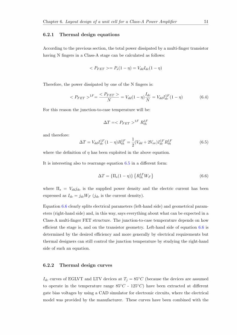
Chapter 6. Layout design of a unit cell for a Class-A Power Amplifier 51
6.2.1 Thermal design equations
According to the previous section, the total power dissipated by a multi-finger transistor
having N fingers in a Class-A stage can be calculated as follows:
< PFET >= Ps(1− η) = VddIdc(1− η)
Therefore, the power dissipated by one of the N fingers is:
< PFET >1F=< PFET >
N= Vdd(1− η)
IdcN
= VddI1Fdc (1− η) (6.4)
For this reason the junction-to-case temperature will be:
∆T =< PFET >1F R1Fth
and therefore:
∆T = VddI1Fdc (1− η)R1F
th =1
2(Vdd + 2Vov)I
1Fdc R
1Fth (6.5)
where the definition of η has been exploited in the above equation.
It is interesting also to rearrange equation 6.5 in a different form:
∆T = Πs(1− η)R1F
th WF
(6.6)
where Πs = Vddjdc is the supplied power density and the electric current has been
expressed as Idc = jdcWF (jdc is the current density).
Equation 6.6 clearly splits electrical parameters (left-hand side) and geometrical param-
eters (right-hand side) and, in this way, says everything about what can be expected in a
Class-A multi-finger FET structure. The junction-to-case temperature depends on how
efficient the stage is, and on the transistor geometry. Left-hand side of equation 6.6 is
determined by the desired efficiency and more generally by electrical requirements but
thermal designers can still control the junction temperature by studying the right-hand
side of such an equation.
6.2.2 Thermal design curves
Idc curves of EGLVT and LTV devices at Tj = 85C (because the devices are assumed
to operate in the temperature range 85C - 125C) have been extracted at different
gate bias voltages by using a CAD simulator for electronic circuits, where the electrical
model was provided by the manufacturer. These curves have been combined with the
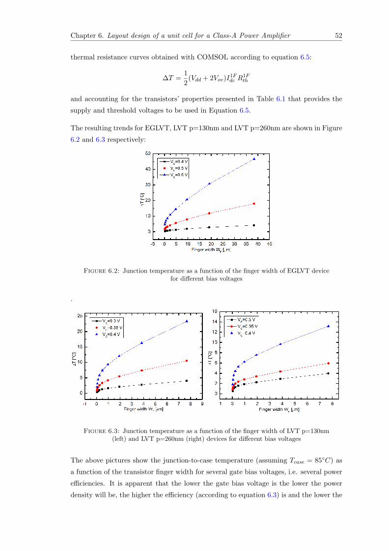
Chapter 6. Layout design of a unit cell for a Class-A Power Amplifier 52
thermal resistance curves obtained with COMSOL according to equation 6.5:
∆T =1
2(Vdd + 2Vov)I
1Fdc R
1Fth
and accounting for the transistors’ properties presented in Table 6.1 that provides the
supply and threshold voltages to be used in Equation 6.5.
The resulting trends for EGLVT, LVT p=130nm and LVT p=260nm are shown in Figure
6.2 and 6.3 respectively:
Figure 6.2: Junction temperature as a function of the finger width of EGLVT devicefor different bias voltages
.
Figure 6.3: Junction temperature as a function of the finger width of LVT p=130nm(left) and LVT p=260nm (right) devices for different bias voltages
The above pictures show the junction-to-case temperature (assuming Tcase = 85C) as
a function of the transistor finger width for several gate bias voltages, i.e. several power
efficiencies. It is apparent that the lower the gate bias voltage is the lower the power
density will be, the higher the efficiency (according to equation 6.3) is and the lower the
Chapter 6. Layout design of a unit cell for a Class-A Power Amplifier 53
junction temperature will be. Therefore a high efficiency oriented design leads to a good
thermal design. Furthermore it should be pointed out the remarkable benefits of using
larger gate-to-gate spacing in terms of lower junction temperatures. However the price
of having both good thermal performance and high efficiency is paid with a higher area
consumption since more fingers and a wider finger spacing are required in order to get
the desired output power and temperature respectively.
Of course, the temperature rise depends on the finger width too since both electric cur-
rent and thermal resistance are affected by that parameter. Electric current is generally
proportional as a power of one to the transistor width, and thus the power handling of
a single finger can be increased just by making it longer, leading to a less total number
of fingers required for a desired output power. On the other hand the finger thermal
resistance is expected to decrease as a function of WF according to Chapter 5.
However the curves in Pictures 6.2 and 6.3 show that the junction to case temperature
rises as a function of the finger width. This means that the decrease of the thermal
resistance is not as strong as the increase of the power handling of each finger. For this
reason there may be a limitation on the maximum finger width, depending on the gate
bias voltage. If, e.g., one wanted to use the EGLVT device biased at Vg = 0.6V , then
the maximum finger width would be around 30µm, provided that the maximum allowed
temperature rise is 40C. No limitations would occur if Vg = 0.3V bias voltage were
adopted (at least in the range of WF shown in the picture). Such geometrical limitations
have to be accounted for in thermal design.
6.2.3 Finger poly-gate resistance limitations
The polysilicon gate resistance contribution given by each finger to the overall gate
resistance (consisting of the contribution due to the interconnects too) has to be kept
under control in order to satisfy RF performance requirements for frequencies around
few GHz. For this reason polysilicon gate resistance may be the actual limiting factor
for the maximum allowed finger width:
|R1F
g | << | 1j2πf0C1F
G
|
R1Fg = αRs
WFL
C1FG ≈ C1F
ox = ϵoxWFLtox
where R1Fg is the distributed poly-gate resistance of each finger, CG is the gate capac-
itance appriximated with the oxide capacitance Cox, f0 is the RF frequency, α is a
correction factor accounting for the distributed nature of the RC network [22], Rs is the
Chapter 6. Layout design of a unit cell for a Class-A Power Amplifier 54
polysilicon sheet resistance, ϵ is the silicon dioxide dielectric constant, tox is the gate
oxide thickness, WF and L are the finger width and length respectively.
The above condition is satisfied if
WF <<
√tox
2πf0αϵoxRs
Assuming that f0 = 2GHz, α = 1/12 (both-side connected gate [23]), Rs = 5 Ωsquare ,
ϵox = 3.9ϵ0 and using the correspondent device geometrical parameters, it follows that:WF << 100µm for LVT devices
WF << 125µm for EGLVT devices
Therefore the maximum finger width is limited by the above values depending on the
device type.
The golden rule adopted in the present work is: WF < 10µm
6.3 Unit cell layout design
In this section the layout of a unit cell for a multi-finger MOSFET power amplifier
based on 28nm FD-SOI technology has been proposed. This design has been used as a
reference for the first tape-out of the Dynamic-ULP project.
6.3.1 Choice of the best device type
The first step to deal with is the choice of the most suitable device for the unit cell
design in terms of acceptable junction temperature and area consumption.
Let’s assume that a Class-A PA requiring 30% power efficiency and 0.5W total output
power has to be designed. The required efficiency would imply a gate bias voltage of
0.35V and 0.5V for LVT and EGLVT devices respectively. Such bias voltages would
lead to the red curves in Figures 6.2 and 6.3 which are reported for convenience in
Figure 6.4 according to the limitation given by the gate resistance. Observe that the
junction-to-case temperature rise is always below the desired value, i.e. 40C, and
therefore temperature is not a limiting factor on the maximum finger width WF . The
limitation comes from the gate resistance whose upper limit is approximately 10µm
according to the previous section but this number is the very limit case. Since the es-
timated maximum finger width does not account for the gate resistance contribution

Chapter 6. Layout design of a unit cell for a Class-A Power Amplifier 55
due to the interconnections it may be wiser to consider a“safer” width value. Therefore
a good choice for the finger width may be WF = 1µm, which has been chosen eventually.
Figure 6.4: ∆T as a function of WF for EGLVT and LVT devices, assuming η = 30%
Table 6.2 summarizes the obtained results for three different designs where the different
physical quantities have been calculated according to the following formulas:
• Power dissipated by a single finger (equation 6.4):
< P 1FFET >= VddI
1Fdc (1− η)
• Power delivered to the load by a single finger:
< P 1Fload >=< P 1F
FET >η
1− η= VddI
1Fdc η
• Total number of fingers required in order to get a desired output power:
N =< Pload >
< P 1Fload >
• Area consumption due to a specific design is (according to the multi-finger tran-
sistor layout shown in Chapter 2):
A = NA1F = NpWF
where WF is the finger width and p is the pitch.
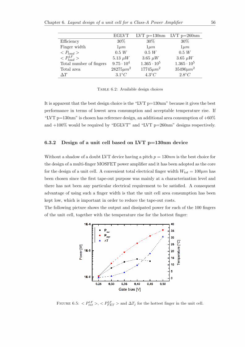
Chapter 6. Layout design of a unit cell for a Class-A Power Amplifier 56
EGLVT LVT p=130nm LVT p=260nm
Efficiency 30% 30% 30%Finger width 1µm 1µm 1µm< Pload > 0.5 W 0.5 W 0.5 W< P 1F
load > 5.13 µW 3.65 µW 3.65 µWTotal number of fingers 9.75 · 104 1.365 · 105 1.365 · 105Total area 28275µm2 17745µm2 35490µm2
∆T 3.1C 4.3C 2.8C
Table 6.2: Available design choices
It is apparent that the best design choice is the “LVT p=130nm” because it gives the best
performance in terms of lowest area consumption and acceptable temperature rise. If
“LVT p=130nm” is chosen has reference design, an additional area consumption of +60%
and +100% would be required by “EGLVT” and “LVT p=260nm” designs respectively.
6.3.2 Design of a unit cell based on LVT p=130nm device
Without a shadow of a doubt LVT device having a pitch p = 130nm is the best choice for
the design of a multi-finger MOSFET power amplifier and it has been adopted as the core
for the design of a unit cell. A convenient total electrical finger width Wtot = 100µm has
been chosen since the first tape-out purpose was mainly at a characterization level and
there has not been any particular electrical requirement to be satisfied. A consequent
advantage of using such a finger width is that the unit cell area consumption has been
kept low, which is important in order to reduce the tape-out costs.
The following picture shows the output and dissipated power for each of the 100 fingers
of the unit cell, together with the temperature rise for the hottest finger:
Figure 6.5: < P 1Fout >, < P 1F
FET > and ∆Tj for the hottest finger in the unit cell.

Chapter 6. Layout design of a unit cell for a Class-A Power Amplifier 57
As can be observed from the picture, the maximum output power condition is when the
gate voltage is 0.4V , i.e. η = 20%. In this scenario the temperature rise is approximately
10C which is far below 40C. It should be pointed out that even in the very limit (and
quite unrealistic) case of a 0% efficiency, i.e. Vg = 0.5V , the temperature rise is still
below 40C, it being approximately 31C. Thanks to such considerations it is possible
to say that the unit cell can be safely operated in Class-A operation withouth any
self-heating problem.
The following table summarizes the unit cell main properties, assuming it is operating
under the maximum output power condition, i.e. η = 20%:
LVT p=130nm
Efficiency 20%Finger width 1µmTotal number of fingers 100< P 1F
load > 4.79 µW< Pload > 479µWTotal area 13µm2
∆T 9.7C
Table 6.3: Unit cell properties
The following pictures show the layout of the proposed unit cell:
Figure 6.6: Layout of the power amplifier’s unit cell
Figure 6.7: Layout of the power amplifier’s unit cell (Detail)

Chapter 6. Layout design of a unit cell for a Class-A Power Amplifier 58
Such an unit cell has been then used for the design of a power amplifier to be manu-
factured in the first tape-out for the Dynamic-ULP project. More specifically ten unit
cells have been placed in parallel in order to get a total number of fingers of 1000 and
therefore a total maximum output power (according to Figure 6.5) of 4.79mW .
The following picture shows the layout of the taped-out Class-A power amplifier based
on the previously designed unit cell:
Figure 6.8: Layout of the taped-out power amplifier
6.3.3 A more accurate evaluation of the junction temperature for the
designed unit cell
In this section the assumption of having a perfect adiabatic boundary condition between
two adiacent fingers made in Chapter 4, i.e. multi-finger structure having an infinite
number of fingers, is verified for LVT device, being the core of the designed unit cell.
A thermal simulation of the entire structure(i.e. 100 transistors placed next to each oth-
ers and an addictional heat spreading region for the same reason mentioned in Chapter
4) would require a huge amount of memory and time, and therefore it is not a feasible
approach. A smarter strategy can be actually implemented in COMSOL, considering

Chapter 6. Layout design of a unit cell for a Class-A Power Amplifier 59
that the temperature profile of a multi-finger MOSFET is basically obtained by super-
imposing the N temperature profiles of each finger, provided that they are shifted by
p, i.e. the gate-to-gate spacing. In order to better understand what this means, let’s
consider the top view of a stand-alone finger, depicted in Figure 6.9.
Figure 6.9: Stand alone finger top view
The temperature peak is reasonably placed at the origin of the shown xyz cartesian
system of axes. In a multi-finger structure the fingers are placed next to each other
along x-axis. Therefore the focus has to be on the temperature profile along the following
straight: y = 0
z = 0
where the undoped silicon thin film is assumed to lie on the plane z = 0.
A reasonable assumption is that the temperature profile of a single finger centered at
x = 0 can be described by a mathematical function TSF (x), symmetric respect to the
z-axis, that is TSF (x) = TSF (−x) (Actually this is an approximation because the heating
rate has a linear profile and therefore it determines a slightly asymmetric temperature
profile according to Chapter 5). Assuming to place N/2 fingers to the left-hand side and
N/2 fingers to the right-hand side of such a finger, the resulting temperature profile will
be:
TN (x) =
n=N/2∑n=−N/2
TSF (x− np) = 2
n=N/2∑n=0
TSF (x− np)

Chapter 6. Layout design of a unit cell for a Class-A Power Amplifier 60
The finger in the middle of the structure, i.e. at x = 0, is the hottest. Therefore, for
the above mentioned symmetries the temperature peak is at x = 0 and the maximum
temperature of a multi-finger MOSFET consisting of N fingers is:
TN (0) = 2
n=N/2∑n=0
TSF (−np) = 2
n=N/2∑n=0
TSF (np) (6.7)
Since it has been estimated that only the neighboring fingers positioned within one
substrate height contribute to cross heating [3] the above series has to be finite, if the
number of fingers N approaches infinite:
limN→+∞
TN (0) = limN→+∞
2
n=N/2∑n=0
TSF (np) = T∞
The temperature profile of the stand alone transistor TSF (x) has been determined with
the help of COMSOL. The simulated geometry is a quarter of the actual one as shown in
figure 6.9 (highlighted by the yellow rectangle). As for the single-finger in a multi-finger
structure in Chapter 4, adiabatic boundary conditions have been placed on the surfaces
of the entire geometry with the exception of the bottom surface, whose temperature has
been fixed at 0K. The geometrical parameters are the same as in Chapter 2 but the
overall simulation region has to be much bigger now, in order to neglect the effect of
virtual devices due to adiabatic boundary conditions.
Figure 6.10: Temperature color map of a stand-alone finger
The temperature peak trend in a multifinger structure as a function of the number
of fingers can be therefore obtained by extracting the temperature profile from the
simulated geometry along the straight y = 0; z = 0 and by using Equation 6.7:

Chapter 6. Layout design of a unit cell for a Class-A Power Amplifier 61
Figure 6.11: Junction temperature as a function of the number of fingers
From Figure 6.11 it is apparent that the assumption of having an infinite number of
fingers is a quite good approximation, it leading to a 10% error in case the actual
number of fingers is 100.
Finally it may be of further interest the evaluation of the errors due to the assumed
uncertainty on the thermal conductivity (kfilms, ksub)and interface thermal resistance
(ITR) values for the designed unit cell, according to the sensitivity analysis section of
Chapter 5. The errors are reported in the following table:
Parameter Uncertainty Error
kfilms 20% 9.7%
ksub 20% 7.5%
ITR 50% 12.4%
Table 6.4: Sensitivity of the unit cell with respect to the parameter’s uncertainty
It is worth noticing how the uncertainty on the parameters does not propagate entirely
into the predicted junction temperature which, for this reason, can be considered very
close to the actual value.

Chapter 7
Conclusions
In the present work the self-heating effects in multi-finger MOSFETs have been investi-
gated thanks to a preliminary study on nano-scale heat conduction and a realization of
a finite element analysis model in the COMSOL Multi-physics environment. Thermal
design guidelines have consequently been proposed and a multi-finger MOSFET power
amplifier unit cell design has been realized.
28nm FDSOI transistors are nano-structures and self-heating effects can be strongly
underestimated if size effects are not taken into account in the finite element analysis
model, according to the simulation results. Quantum mechanical effects are responsible
for the reduction of the thermal conductivity in very thin crystal/polycrystals films
because of an enhanced boundary scattering of phonons. Moreover the imperfections
at the interface between two layers bring an additional contribution in the reduction
of the device thermal performance, leading to an interface thermal resistance. The
heat generation region in a MOSFET device has to be considered according to the
Joule Heating model. If a uniform heat generation region is assumed beneath the gate
oxide, an error up to 10% has been observed in the junction temperature resulting
from thermal simulations. As a verification on the credibility of the obtained results,
a sensitivity analysis on the simulation results has been performed with respect to an
assumed uncertainty on the adopted parameters. It has been shown that the simulation
results deviate of a percentage which is lower than the assumed uncertainty on the
parameters, i.e. 20% for the thermal conductivity values and 50% for interface thermal
resistance. For this reason the predicted junction temperature has to be reasonably very
close to the actual value.
From a geometrical perspective, simulations has shown that the junction temperature
(or the single finger thermal resistance) is strongly affected by the finger width WF and
by the spacing between adjacent fingers p. The physical explaination of this result could
62

Conclusions 63
be that the spacing reduces the strength of the thermal interaction between adiacent
fingers, while, on the other hand, the finger width enhances the heat dissipation through
the substrate. The junction temperature trend respect to the geometrical parameters is
thus confirmed by common sense and by the works reported by several authors.
Afterwards, thermal design guidelines for Class-A power amplifiers have been proposed,
based on thermal design equations and curves, which have been obtained by coupling
electrical and thermal equations. More specifically several electrical bias conditions
(several power efficiencies) have been coupled with thermal equations in order to get
temperature curves as a function of the pitch and the transistor finger width. In this
way it has been possible to compare the thermal performances for EGLVT and LVT
devices and determine which of them could give the best trade-off in terms of acceptable
junction temperature and area consumption.
LVT device having a pitch p = 130nm has been found to be the best choice for the
design of a multi-finger MOSFET power amplifier and it has been adopted as the core
for the design of a unit cell. Such an unit cell has been used for the design of a power
amplifier to be manufactured in the first tape-out for the Dynamic-ULP project.
As a further check on the predicted junction temperature of the designed power amplifier
a more accurate thermal simulation has been performed, accounting for the finite number
of fingers wherewith the amplifier has been realized. The result of this further simulation
has been that the approximaton of having an infinite number of fingers leads to an
overestimation of just 10% on the predicted junction temperature. Such a percentage
falls within the uncertanty of the adopted parameters and for this reason, the infinite
fingers approximation can still be considered a good model.

Bibliography
[1] Zhang K. and Cheng M. C. “Thermal Circuit for SOI MOSFET Structure Ac-
counting for Nonisothermal Effects ”. IEEE Transactions on Electron Devices, 57
(11):2838–2847, November 2010.
[2] Sangiorgi E. Fiegna C., Yang Y. and ONeill A.G. “Analysis of Self-Heating Effects
in Ultrathin-Body SOI MOSFETs by Device Simulation”. IEEE Transactions on
Electron Devices, 5(1):233–244, January 2008.
[3] Bayba A. J. Darwish A. M. and Hung H. A. “Accurate Determination of Thermal
Resistance of FETs”. IEEE Transactions on Microwave theory and techniques, 53
(3):306–313, January 2005.
[4] Hussin R. Asheghi M. Liu W., Etessam-Yazdani K. “Modeling and Data for Ther-
mal Conductivity of Ultrathin Single-Crystal SOI Layers at High Temperature”.
IEEE Transactions on Electron Devices, 53(8):1868–1876, August 2006.
[5] Komarov P. L. Burzo M. G. and Raad P. E. “Thermal Transport Properties of
Gold-Covered Thin-Film Silicon Dioxide”. IEEE Transactions on Components and
packaging technologies, 26(1):80–88, March 2003.
[6] Dutton R. W. Pop E., Rowlette J. A. and Goodson K. E. “Joule Heating under
Quasi-Ballistic Transport Conditions in Bulk and Strained Silicon Devices”. Sim-
ulation of Semiconductor Processes and Devices, pages 307–310, September 2005.
[7] Krishna S. “Effect of Gate Resistance on High-Frequency Power Switching Efficien-
cies of Advanced Power MOSFET’s ”. IEEE Journal of Solid-State Circuits, 25(2):
595–601, April 1990.
[8] Kittel C. and Kroemer H. “Thermal Physics”, volume ISBN 0-7167-1088-9. W.H.
Freeman, San Francisco, second edition.
[9] Lienhard IV J.H. and Lienhard V J.H. “A heat transfer textbook’. Phlogiston Press,
Cambridge - Massachussets, third edition, 2008.
64

Bibliography 65
[10] Kittel C. “Introduction to Solid State Physics’. John Wiley & Sons, Inc, eighth
edition, 2004.
[11] Dutton R. Pop E. and Goodson K. “Thermal Analysis of Ultra-Thin Body Device
Scaling”. Electron Devices Meeting. IEDM ’03 Technical Digest. IEEE Interna-
tional, December 2003.
[12] Uma S. McConnell A. D. and Goodson K.E. “Thermal Conductivity of Doped
Polysilicon Layers”. Journal of Microelectromechanical Systems, 10(3):360–369,
September 2001.
[13] Tian L. Liu L. Zhichao L., Yuan J. and Li Z. “Measurement of the Thermal
Conductivity of Undoped Polysilicon Thin Film Over 300K to 400K”. Solid-State
and Integrated Circuits Technology, 2004. Proceedings, 3:2190–2193, October 2004.
[14] Lee T. Burzo M. G., Raad P. E. and Komarov P. L. “Thermal Conductivity
Measurements of Novel SOI Films Using Submicron Thermography and Transient
Thermoreflectance”. 28th IEEE SEMI-THERM Symposium, pages 150–156, March
2012.
[15] Katayama S. Yamane T., Nagai N. and Todoki M. “Measurement of thermal con-
ductivity of silicon dioxide thin films using a 3 ω method”. Journal of Applied
Physics, 91(12):9772–9776, June 2002.
[16] Walkey D.J. Beggs B.C. Reimer C. J., Smy T. and Surridge R. “A Simulation Study
of IC Layout Effects on Thermal Management of Die Attached GaAs ICs”. IEEE
Transactions on Components and packaging technologies, 23(2):341–352, June 2000.
[17] Bai C. and Veatch M. “Chip Scale Package Design for Thermal Performance in
Mobile Handsets”. Electronic Components and Technology Conference, pages 1415–
1419, 2007.
[18] Lee T. Burzo M. G., Raad P. E. and Komarov P. L. “Thermal Conductivity
Measurements of Novel SOI Films Using Submicron Thermography and Transient
Thermoreflectance”. 28th IEEE SEMI-THERM Symposium, pages 150–156, March
2012.
[19] Huang Z. Bai S., Tang Z. and Yu J. “Thermal Characterization of Si3N4 Thin Films
Using Transient Thermoreflectance Technique”. IEEE Transactions on Industrial
Electronics, 56(8):3238–3243, August 2009.
[20] Wilson J. and Decker K. “GaAs MMIC Thermal Modeling for Channel Temper-
atures in Accelerated Life Test Fixtures and Microwave Modules”. 10th IEEE
SEMI-THERM Symposium, pages 121–128, February 1994.

Bibliography 66
[21] Antoniadis D. A. Goodson K. E. Su L. T., Chung J. E. and Flik M. “Measurement
and Modeling of Self-Heating in SOI NMOSFETs”. IEEE Transactions on Electron
Devices, 41(1):9772–9776, January 1994.
[22] Bhattacharya E. Raman M. S., Kie T. and Bhat K. N. “Physical Model for the
Resistivity and Temperature Coefcient of Resistivity in Heavily Doped Polysilicon”.
IEEE Transactions on Electron Devices, 53(8):1885–1892, August 2006.
[23] Chen C. H. Liu W. Deen M. J. Gray P. R. Jin X., Ou J. J. and Hu C. “An Effective
Gate Resistance Model for CMOS RF and Noise Modeling”. IEEE Electron Devices
Meeting, pages 961–964, December 1998.