Embed Size (px)
Citation preview

1
Supporting Information
Thermoelectric Properties of PEDOT Nanowires/PEDOT
HybridsKun Zhang,a Jingjing Qiub, Shiren Wang*a aDepartment of Industrial and Systems Engineering, Texas A&M University, College
Station, TX 77843, USA
bDepartment of Mechanical Engineering, Texas Tech University, Lubbock, TX 79409-
1021, USA
E-mail: [email protected]
1. Materials and Methods1.1 Synthesis of PEDOT nanowires[1]
Sodium dodecyl sulfate (SDS, 30 mmol, Sigma-Aldrich, ≥99%) was dissolved in
deionized (DI) water (100 ml). Subsequently, an aqueous solution of iron (III) chloride
FeCl3 (16.33 mmol, Sigma-Aldrich, ≥97%) was added to the SDS solution and stirred
for 1 h at 50 oC. Then 3,4-ethylenedioxythiophene monomer (EDOT, 7 mmol, Sigma-
Aldrich, 97%) was slowly added to the solution and the resultant solution was left on a
hot plate to allow for polymerization for 6 h at 50 oC. After polymerization, the resultant
PEDOT nanowire solution was purified with methanol and DI water for several times and
then immediately re-dispersed in methanol with the aid of ultrasonication. In order to
improve the dispersion of PEDOT nanowires, 5 vol% dimethyl sulfoxide (DMSO,
Sigma-Aldrich, ≥99.5%) was added into PEDOT nanowire/methanol solution with
another 15 min ultrasonication. The electrical conductivity of PEDOT nanowires film
was measured to be ~450 S/cm.
1.2 Preparation of PEDOT NWs/PEDOT:PSS composite films
Electronic Supplementary Material (ESI) for Nanoscale.This journal is © The Royal Society of Chemistry 2016

2
PEDOT:PSS (H. C. Starck) was filtered by a syringe filter (0.45 micron pore-size
PVDF syringe filter) and mixed with 5 vol% DMSO for the subsequent process. 13.3 mg
PEDOT nanowires (4 ml PEDOT nanowire/methanol/DMSO solution) was mixed with
10 ml PEDOT:PSS/5 vol% DMSO and subjected to 15 min ultrasonication. The thin film
was prepared by spin-coating PEDOT nanowire/ PEDOT:PSS/5 vol% DMSO solutions at
4000 rpm for 40 seconds on a 13 mm ×13 mm glass substrate pre-cleaned with detergent,
DI water, acetone and isopropanol in sequence. After spin-coating, the sample was
thermally annealed at 130 oC for 15 min on a hot plate, and was subsequently immersed
in ethylene glycol (EG, Sigma-Aldrich, anhydrous, 99.8%) solvent for a specific time at
room temperature (50, 120, 220 and 300 min). After EG treatment, the sample was rinsed
and washed in DI water to remove residual EG solvent. Finally, the treated sample was
annealed on a hot plate at 120 oC for another 15 min.
1.3 Preparation of PEDOT NWs/PEDOT-Tos composite films
PEDOT-Tos thin films were prepared via a vapor-phase polymerization (VPP) method
reported elsewhere. [2-3] In a typical procedure, 2 g Clevios™ C-B 40 V2 (40 wt% Iron
(III) tosylate (Fe(Tos)3) in n-butanol), 1.5 g PEG-PPG-PEG (Mw=5800, Sigma-Aldrich)
and 1.5 g dimethylformamide (DMF, Sigma-Aldrich) and 1.5 g n-butanol were pre-
mixed. The tripolymer PEG-PPG-PEG and DMF were used to control the crystallization
of PEDOT. The mixture was ultrasonicated for 10 min to mix thoroughly. Microscope
glass slides were cut into 13 mm by 13 mm and washed with detergent, DI water, acetone
and isoproponal in sequence. These washing steps help the oxidant solution to wet the
glass substrate. The vial with oxidant solution was placed on a hotplate at 35 oC for ~2
minutes prior to pipetting solution. Subsequently, the oxidant solution was dropped and

3
covered the entire glass substrate. Then the substrate was spin-coated at 1500 rpm for 25
sec and immediately transferred onto a hotplate at 70 oC for 30 sec. Finally, the substrate
was transferred to a vacuum oven with a crucible having EDOT monomers at the bottom
of the chamber. The vapor-phase polymerization was conducted in the chamber at 35 oC
under a pressure of 45 mbar. After 25 min, the sample was removed from the chamber
and placed on a hotplate at 70 oC for 2 min and then cooled down to room temperature.
The resultant PEDOT-Tos thin film was thoroughly washed with ethanol to remove any
oxidant residuals. The washed film was finally dried in air for further characterization. To
fabricate PEDOT NW/PEDOT-Tos composite film, 0.2 wt% PEDOT NWs were added
into the above oxidant solution with tip ultrasonication for 1 hour. Other steps are
identical to that of the fabrication of PEDOT-Tos films.
2. Structure characterizations
The PEDOT nanowire structure was characterized by transmission electron
microscope (TEM, Hitachi 8100, 75 kV, Figure 1), X-ray diffraction (XRD, Figure 1),
and atomic force microscope (AFM, XE-100, contact mode with the scanning rate=1 Hz,
Figure S1). The XRD patterns were collected with Powder X-Ray Diffraction (PXRD)
with a Rigaku Ultima III diffractometer using Cu Kα radiation. To prepare the samples
for X-ray powder diffraction, samples were finely ground. The measurements were taken
at a 2θ range of 5-40° at a step-width of 0.03° sec-1.

4
Figure S1. AFM topography images of PEDOT NWs/PEDOT:PSS hybrid films with
various PEDOT NW weight fractions. a, 0.1 wt%. b, 0.2 wt%. c, 0.5wt%. d, 1 wt%.
Samples with high NW fraction (0.5 and 1 wt%) hybrids show percolated networks.
3. Carrier mobility measurement by organic electrochemical transistors (OECTs)
We firstly made several trials with standard organic field-effect transistor (OFET)
devices for the mobility measurement of highly doped PEDOT samples, however, no
field effects were observed, which also has been reported in the literature.[7] In this work,
the linear carrier mobility of PEDOT samples were evaluated with the side-gate OECTs
as reported in the literature.[7-8] The side-gate OECT architecture is utilized because
1 μm 1 μm
1 μm 1 μm
a b
c d

5
PEDOT:PSS is highly doped with the carrier concentration typically more than 1020 cm-3,
which could screen the electric field in standard OFET devices.[7] In standard OFET
architecture (i.e. bottom-gate bottom-contact), the carriers are accumulated at the
interface between the active semiconductor layer and the dielectric layer by applying a
electric field at the gate. But in PEDOT:PSS, carriers are always present due to its high
doping level. For this reason applying a field doesn't have much effect as the existing free
carriers simply respond to an externally applied field by moving towards the lowest
energy level and therefore shield the material from the field. In some low doping levels of
PEDOT:PSS there may still be a small field effect, but in highly doped PEDOT:PSS,
such as PEDOT:PSS, there is unlikely to be any effect. Hence, this is the reason why we
conducted the linear carrier mobility measurements with electrolyte-gated
electrochemical transistors. Further evidence will be provided to explain the reliability of
measuring linear mobility with OECT devices.
Here, a side-gate OECT architecture was used to measure the linear carrier mobility
of highly doped PEDOT:PSS as reported in the literature.[7-8] Ion gel was used to
introduce a higher density of charge carriers. As shown in Figure S2, transistors with a
channel length (L) of 50 μm and width (W) of 6 mm were fabricated in a bottom-contact
side-gate configuration on the SiO2 substrates. Au was used for the source, drain, and
gate electrodes. Ion gels based on poly(vinylidene fluoride-co-hexafluoropropylene)
(P(VDFHFP)) and the ionic liquid 1-ethyl-3-methylimidazolium
bis(trifluoromethylsulfonyl)amide ([EMI+][TFSA-]) were used as the dielectric layer. The
thickness of PEDOT:PSS layer is 20–50 nm, and the thickness of ion gel dielectric layer
is ~ 6 μm.

6
Ion gelS PEDOT:PSS D G
Glass
VD VG
Figure S2. Illustration of side-gate OECT device for the linear carrier mobility
measurement. S: Source electrode, D: Drain electrode, G: Gate electrode. VD: Source-
drain voltage, VG: Gate voltage.
The active layer of OECT devices was formed by spin-coating with a uniform thin
layer (<50 nm). Cotton swabs soaked in solvents (ethanol for PEDOT:PSS) were used to
thoroughly wipe clean contact pads and the rest of the substrates with the exception of the
area around the channel. A high precision cotton swab was used to clean between devices
to avoid cross-talking and reduce leakage.
Two Keithley 2400 source-meters were used both to provide gate and drain voltages,
and also as the drain-source current meter by connecting the gate and drain socket on the
probe station to two Keithley 2400 using two shielded coaxial cables. In general the
Keithley 2400 is used as a voltage source and current is measured on auto range with a
compliance of ~1 mA. The linear mobility is calculated from the following ( )lin
equation:[7]

7
( ) d
i G
L glinW C V
where Ci (=12 μF/cm2 at 1 Hz) is the dielectric capacitance per unit area of the ion gel
dielectric layer,[7] the capacitance will decrease as the measured frequency increases;[8,9]
gd =ID/VD is the conductance, which was calculated using the linear regime (small drain
voltage) of output curves when the gate voltage is small that the ions in ion gels haven’t
penetrated and dedoped the polymer channel, ID is the source-drain current, VD is the
source-drain voltage, VG is the gate voltage, L =50 μm and W=6 mm are the channel
length and width. Figure S3 shows typical output characteristics and conductance of
PEDOT-based OECT devices for linear mobility evaluation. (Note: Several same
samples were measured for each type of OECT device.) Linear mobility results are
shown in Table S1.
As shown in Figure S3a, clear field effect can be observed in all samples, which
should be due to the de-doping of PEDOT samples as the gate voltage is high, which has
been experimentally verified by Wei et al with the in situ UV–vis–NIR spectroscopy.[7]
The electrochemical doping mechanism also has been extensively studied in poly(3-
hexylthiophene) (P3HT) or other organic semiconductors-based electrolyte-gated OECT
devices.[10-12]

8
Figure S3. a, Output curves of the OECT using 5 vol% DMSO/PEDOT:PSS as the active
channel. b, Conductance curves as a function of gate voltage for OECT using 5 vol%
DMSO/PEDOT:PSS as the active channel.
As displayed in Figure S3b, the conductance was plotted as a function of gate
voltage. As the gate voltage is low, the conductance gd shows linear decrease as the
positive gate voltage increases, which should be attributed to the linear decrease of carrier
concentration in polymer channels. The carriers in this regime should comply with a
two-dimensional transport at the interface between PEDOT channels and ion gels.[10,12]
As the gate voltage is large enough, the ions in ion gels can penetrate into PEDOT
channels introducing the electrochemical de-doping of PEDOT samples. It is believed to
follow with the three-dimensional charge transport, indicating the carriers are transported
through the bulk of PEDOT materials.[10] As seen in Figure S3b, as the applied gate
voltage increases, there are inflection points in all samples that the electrochemical de-
doping of PEDOT samples resulted in dramatic decreasing of the conductance with a
larger slope. It is worth to note that the diffusion of ions into the bulk of PEDOT channels
depends not only on the gate voltage but also on the scanning rate of gate voltage. A long
enough time at low gate voltage would also result in the diffusion of ions. So a proper
VG from 0 to 3 VStep 0.1 V
Slope: 2.73×10⁻³

9
scan rate of gate voltage was used (0.1V/s). Moreover, it can be seen that there is no
saturation regime for these PEDOT-based transistors, thus only the evaluation of linear
carrier mobility in the linear regime is plausible. And based on the two-dimensional
transport in this regime, the formula for the linear mobility calculation in organic field-
effect transistors is valid in this work.
Table S1. Averaged linear carrier mobility results of PEDOT:PSS, PEDOT-Tos,
PEDOT:PSS /5 vol% DMSO with various EG treatment times.
Samples μ (cm2/Vs)
5 vol% DMSO/PEDOT:PSS, EG 0 min 2.02±0.11
5 vol% DMSO/PEDOT:PSS, EG 50 min 2.41±0.26
5 vol% DMSO/PEDOT:PSS, EG 120 min 3.18±0.35
5 vol% DMSO/PEDOT:PSS, EG 220 min 3.51±0.18
PEDOT:Tos 1.78±0.13
Note: For all EG treated PEDOT:PSS, 5 vol% DMSO was added before spin-coating.
4. Work function measurement
Work functions (WFs) of the polymer samples were measured with both x-ray
photoelectron spectroscopy (XPS) and Kelvin probe, with the results using both methods
showing good agreement. It was found by Kelvin probe (KP) method that PEDOT NW
samples have a very similar work function except PEDOT NW with 220 min EG
treatment, so we use a single average work function value for PEDOT NW with 0, 50,
120 and 300 min EG treatment. So the work function offsets between PEDOT:PSS and
PEDOT NW were calculated based on the Kelvin probe method, see Table S2 for details.
Kelvin probe work function measurements were performed on an SKP SPV LE 450
Scanning Kelvin Probe Surface Photovoltage instrument from KP Technology. KP
measurements were performed in air with a probe oscillation frequency of 78 kHz. The

10
XPS work function measurements were performed in ultrahigh vacuum on a PHI 5600
ESCA instrument, which has been discussed previously.[13] We note that the secondary
electron cutoff region is photon energy independent. Thus, we calibrated the energy scale
for the secondary electron cutoff region using ultraviolet photoelectron spectroscopy
(UPS) with known metallic standards (Au, Mo, Cu, or Ag), which results in an
uncertainty of +/- 0.025 eV for the extracted work function. The work function for each
sample was determined by measuring the secondary-electron cut-off region. Specifically,
we fit the baseline and secondary-electron cut-off to a line; the intercept of the two
determines the work function (work function = 21.218 eV – intercept). Interestingly, in
some samples, the secondary electron cutoff region has a small additional shoulder at
higher binding energy. The origin of this shoulder is unclear, but may be due to a
minority phase within the material. In all samples, we fit the secondary electron cutoff
that represents the majority of the signal to ensure consistent comparisons for the sample
work functions. Work functions were referenced to three different metallic samples –
platinum, gold, and Inconel – that were stored in air and were not rigorously cleaned
before XPS or KP measurements. The work functions of the reference samples were
determined by XPS to be 5.13, 5.03, and 4.37 eV for platinum, gold, and Inconel,
respectively. The work function of a given polymer sample was calculated from the linear
regression fit to the standards, as shown in Figure S4.

11
Figure S4. Calibration curve for Kelvin probe measurement, based on XPS-measured
work function values for three reference samples: gold, platinum, and Inconel (gold data
points). A given polymer sample’s work function is calculated from the measured Kelvin
probe potential difference (KP), using the equation determined by the linear regression fit
shown as the solid line.
Table S2. Work functions of as-received PEDOT:PSS, PEDOT-Tos, 5 vol%
DMSO/PEDOT:PSS with different EG treatment times.
EG treatment time
(min)
WF of 5 vol% DMSO/PEDOT:PSS
(eV)
WF of PEDOT NWs
(eV)
Interfacial barrier ∆E (eV)
0 4.88 4.78 0.10
50 4.92 4.78 0.14
120 4.87 4.78 0.09
220 4.85 4.78 0.07
300 4.82 4.78 0.04
PEDOT:Tos 4.63 4.78 -0.15

12
5. Thermoelectric properties characterizations
5.1 The electrical conductivity measurement
The Van der Pauw method was employed for electrical conductivity measurements
(Figure S5). Electrical contacts were made by thermally depositing gold electrodes (1.5
mm by 1.5 mm) on four corners of the thin film on glass substrate. I-V sweeps were
performed using a Keithley 6221 current source and a Keithley 2182A nanovoltmeter.
DC current was applied from corner 2 to corner 1, and the voltage was measured between
corner 3 and corner 4, RA was calculated as (V3,4/I1,2 + V1,2/I3,4)/2. DC current was applied
from corner 3 to corner 2, and the voltage was measured between corner 1 and corner 4,
RB was calculated as (V1,4/I2,3 + V2,3/I1,4)/2. By measuring RA and RB, the electrical
conductivity can be calculated by the following equation: [14]
-1( ) ( )
ln 2 2A B A
B
d R R RfR
,where d is the film thickness (measured by AFM, XE-100), f(x)=1/cosh(ln(x)/2.403) is
the correction factor.[14]

13
Figure S5. Illustrations of the Van der Pauw method for electrical conductivity
measurements. a, Schematic diagram of the Van der Pauw method. b, Photo of the Van
der Pauw measurement system.
5.2 The Seebeck coefficient measurement[15,16]
To determine the Seebeck coefficient of conducting thin films, a Peltier heater was used
to heat one side of thin films, a Peltier cooler was used as the heat sink to cool another
side of thin film (Figure S6). The relative humidity is ~17% during measurements. Prior
to the measurement, a pair of square gold electrodes (1 mm × 7 mm × 150 nm) with the
spacing l of 10 mm was thermally deposited on each film to define the electrical
measurement spacing. Two T-type micro-thermocouples (TCs, diameter of 127 μm) were
placed on the thin film to the left of the left electrode and to the right of the right
electrode with a spacing of L, which is much larger than the TC diameter, and the error in
TC position. Polymer in the region of the TCs was erased by a hard swab with ethanol in
order to eliminate the interruption to the thermal voltage measurement. The measured
temperature difference between TCs was defined as ∆TTC, thus the actual temperature

14
difference between electrodes is ∆T=∆TTC×l/L. Further experiments and simulation
proved that the temperature profile along the direction of TCs is linear. To measure the
Seebeck voltage ∆V, two gold micro-wires (diameter of 25 μm) were brought into contact
with the gold electrodes with the assistance of indium. The Seebeck coefficient is thus
defined as S= -∆V/∆T.
TC1 TC2
Au Au
Glass
Heater Heat sink
Voltage
PEDOT:PSS thin film
Figure S6. Illustrations of the Seebeck coefficient measurement. a, The side-view of the
Seebeck coefficient measurement setup. b, The schematic diagram of the Seebeck
coefficient measurement setup assembling.
Prior to the Seebeck coefficient measurement, the one-dimensional temperature
distribution across the thin film surface was investigated. For a barrier with a constant
thickness, the rate of heat loss is given by:
( )
( )
hot cold
hot cold
Q A T Tt d
T T Qd t A
,where Q is the heat flux, t is the unit time, κ is the thermal conductivity of thin film, Thot
is the hot side temperature, Tcold is the cold side temperature, A is the cross-sectional area
of the thin film, and d is the distance between the hot side and the cold side.
a b
15
For a direct current (DC) powered heat source (Peltier heater), the heat flux Q is
constant for unit time. For a given sample, the thermal conductivity κ and the cross-
sectional area A are also constant. Thus the temperature difference per unit length (Thot -
Tcold)/d is constant for the thin film. Hence the one-dimensional temperature distribution
is linear from the hot side to the cold side.
To demonstrate this linear temperature distribution, temperatures of four selected
points on the thin film were measured. As illustrated in the inset of Figure S7a, four T-
type micro-thermocouples (TCs, diameter of 127 μm) were placed collinearly with
various distances (which is much larger than the TC diameter and the error in TC
position) between each other on the thin film. (Note: In order to avoid the effect of heater
and cooler on the accuracy of the temperature measurements, TCs were placed away
from the heater and cooler edges with a distance of > 2 mm.) When the temperature was
stable, temperatures were collected and found to vary linearly with respect to the distance
between the TC position (where the temperatures were measured) and the heater edge
(Figure S7a). Temperatures with respect to the distance between the TC position and the
heater edge were captured for 12 min and found to be linear at a specific time (Figure
S7b). The same trend was found through the temperature simulation as seen in Figure S8.

16
2 4 6 8 1024
25
26
27
Tem
pera
ture
(o C)
X (Distance to the heater edge, mm)
2 4 6 8 1024
25
26
27
Tem
pera
ture
(o C
)
X (Distance to the heater edge, mm)
12 m
in
Figure S7. Linear temperature distributions across the polymer thin film on glass
substrate. a, The measured temperature distribution in a line vertical to the heating
direction with respect to the distance between the location where the temperature was
measured and the heater edge as shown in the inset. b, The temperature distribution with
respect to the distance between the location where the temperature was measured and the
heater edge during 12 min heating time.
0 2 4 6 8 10 1221
22
23
24
25
Tem
pera
ture
(o C)
X (Distance to the heater edge, mm)
Figure S8. Simulated temperature distribution across thin film on glass substrate. a, The
simulated temperature distribution in a line vertical to the heating direction with respect
a b

17
to the distance between the location where the temperature was measured and the heater
edge. b, The side-view of the simulated temperature profile.
Table S3. Measured Seebeck coefficients of selected samples with (S1) or without (S0)
the addition of 0.2 wt% PEDOT NWs under the same EG treatment time.
Samples S0 (μV/K) S1 (μV/K)
5 vol% DMSO/PEDOT:PSS, EG 0 min 13.6±3.3 22.8±2.0
5 vol% DMSO/PEDOT:PSS, EG 50 min 23.4±5.1 35.8±2.2
5 vol% DMSO/PEDOT:PSS, EG 120
min
22.2±1.8 38.9±1.0
5 vol% DMSO/PEDOT:PSS, EG 220
min
25.6±5.2 37.2±4.3
5 vol% DMSO/PEDOT:PSS, EG 300
min
25.6±2.3 35.4±3.6
PEDOT-Tos 46.7±3.5 55.6±3.0
Note: The Seebeck coefficient ratio S1/S0 is defined as the ratio of Seebeck coefficient of the
PEDOT:PSS matrix with (S1) and without (S0) the addition of PEDOT NWs under the same EG
treatment time.
18
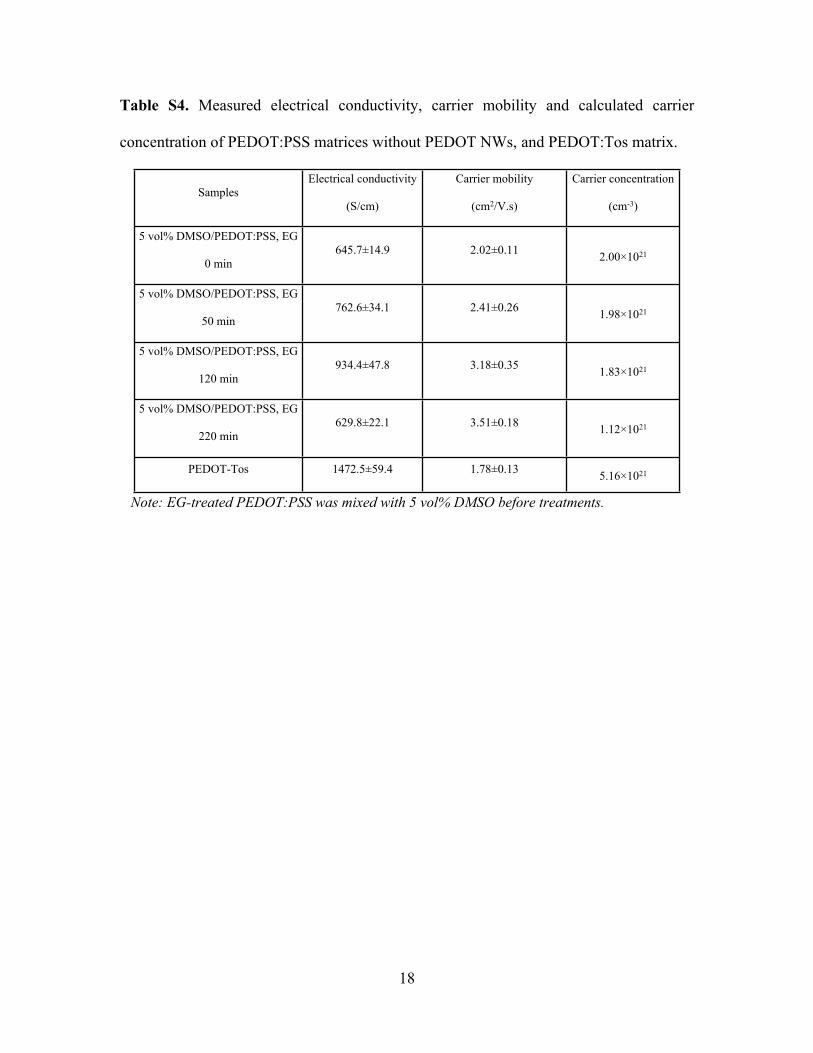
Table S4. Measured electrical conductivity, carrier mobility and calculated carrier
concentration of PEDOT:PSS matrices without PEDOT NWs, and PEDOT:Tos matrix.
SamplesElectrical conductivity
(S/cm)
Carrier mobility
(cm2/V.s)
Carrier concentration
(cm-3)
5 vol% DMSO/PEDOT:PSS, EG
0 min645.7±14.9 2.02±0.11 2.00×10²¹
5 vol% DMSO/PEDOT:PSS, EG
50 min762.6±34.1 2.41±0.26 1.98×10²¹
5 vol% DMSO/PEDOT:PSS, EG
120 min934.4±47.8 3.18±0.35 1.83×10²¹
5 vol% DMSO/PEDOT:PSS, EG
220 min629.8±22.1 3.51±0.18 1.12×10²¹
PEDOT-Tos 1472.5±59.4 1.78±0.13 5.16×10²¹
Note: EG-treated PEDOT:PSS was mixed with 5 vol% DMSO before treatments.

19
0.0 0.2 0.4 0.6 0.8 1.00
10
20
30
40
0 min, E=0.10 eV
S
(V
K-1)
PEDOT nanowire fraction (wt%) 0
0.0 0.2 0.4 0.6 0.8 1.00
200
400
600
800
0
(S
cm-1
)
PEDOT nanowire fraction (wt%)
0.0 0.2 0.4 0.6 0.8 1.00
10
20
30
40
50
PEDOT nanowire fraction (wt%)
S2
(W
m-1
K-2
)
Figure S9. Thermoelectric properties of PEDOT NWs/PEDOT:PSS hybrids without EG
treatments. a, Seebeck coefficient. b, Electrical conductivity. c, Power factor PF of
PEDOT:PSS hybrids. Note: PEDOT:PSS was mixed with 5 vol% DMSO before
treatments.
6. Thermal conductivity measurements
6.1 Specific heat measurements
The specific heat of polymers was calculated using DSC spectra performed with
METTLER TOLEDO thermal analysis system with the measurement error of 3.7 %. 40
μl aluminum crucibles were chosen as reference, blank and sample crucibles for good
c
a b

20
thermal contact between samples and the bottom of crucible. The reference crucible was
maintained in the same position for all measurements. Different PEDOT:PSS composites
were prepared and dried in the same condition as that for thermoelectric property
measurements . The composites were cold-pressed into small pellets for better thermal
contact with the crucible bottom. The sample weight ranging from 4 to 7 mg was loaded
for higher accurate measurements. The temperature ranges from 0 to 60 oC with an initial
isothermal stage at 0 oC for 3 min, then the sample was heated up with the heat rate of 10
oC /min from 0 oC to 60 oC. By recording the heat flow rate as a function of temperature
and subtracting the heat flow rate for the blank crucible (blank curve) under the same
condition, the specific heat at room temperature is determined using the formula
Cp=HF/mβ, where HF is the heat flow rate for the measured sample, m is the mass of the
sample (mg), and β is the heating rate (oC /min).
6.2 Thermal diffusivity measurements
It is challenging to measure the thermal diffusivity of nanoscaled-thick polymer films,
thick polymer films (~20 μm) were prepared by drop-casting polymer solution on
aluminum alloy 6061-T6 (1.5 mm thick) and treated in the same condition as that for
thermoelectric property measurements. Laser flash technique was applied to measure the
thermal diffusivity of PEDOT nanowire/PEDOT:PSS composites. The thermal diffusivity
measurement was performed by using a two-layer method with Netzsch LFA 447 with a
theoretical error of ~10%.[17]
The film density ρ=m/V was determined by measuring the film volume V (thickness ×
length ×width) and mass m. The thickness was measured by SEM (Hitachi 4300, 10 kV).
21
Finally, the thermal conductivity is calculated by κ=ραCp, where ρ is the density (g
cm-3), α is the thermal diffusivity (mm2 s-1), and Cp is the specific heat (J g-1 K-1).
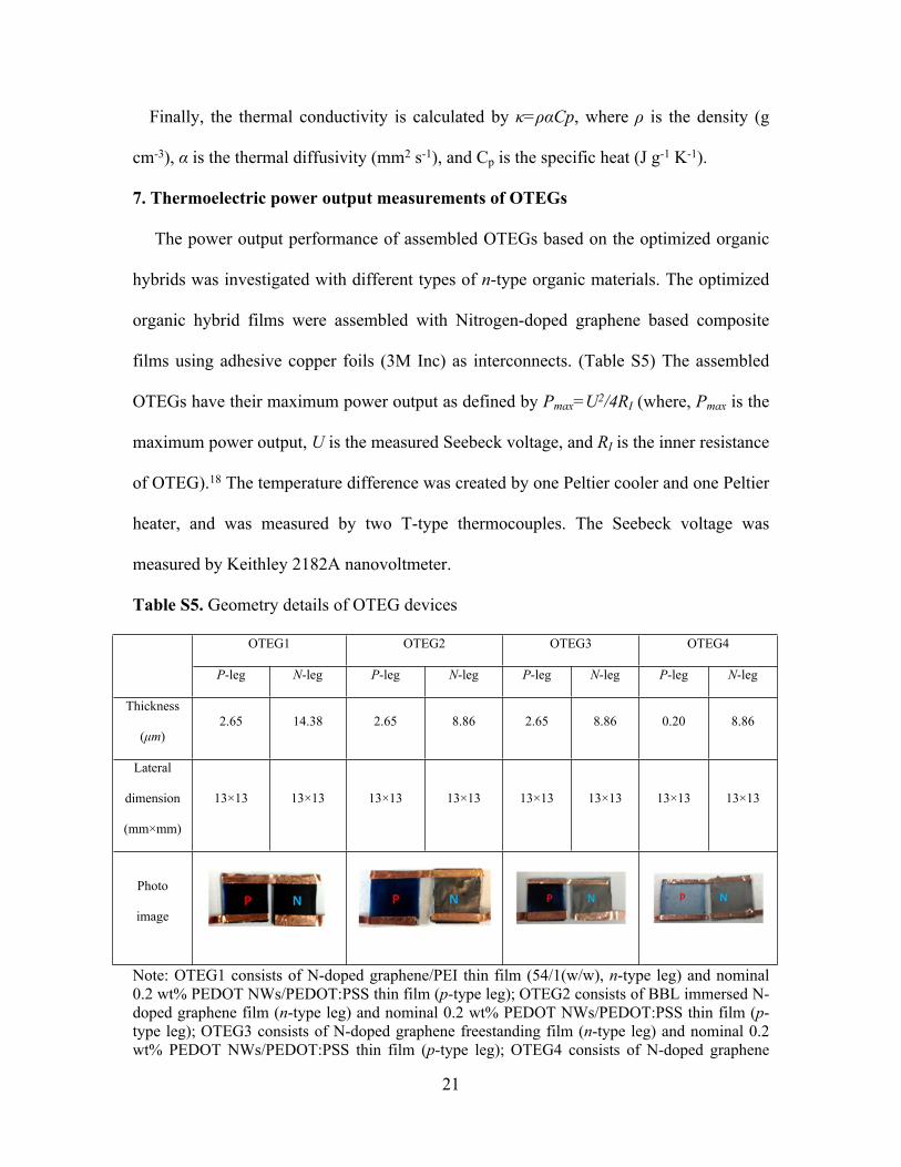
7. Thermoelectric power output measurements of OTEGs
The power output performance of assembled OTEGs based on the optimized organic
hybrids was investigated with different types of n-type organic materials. The optimized
organic hybrid films were assembled with Nitrogen-doped graphene based composite
films using adhesive copper foils (3M Inc) as interconnects. (Table S5) The assembled
OTEGs have their maximum power output as defined by Pmax=U2/4RI (where, Pmax is the
maximum power output, U is the measured Seebeck voltage, and RI is the inner resistance
of OTEG).18 The temperature difference was created by one Peltier cooler and one Peltier
heater, and was measured by two T-type thermocouples. The Seebeck voltage was
measured by Keithley 2182A nanovoltmeter.
Table S5. Geometry details of OTEG devices
OTEG1 OTEG2 OTEG3 OTEG4
P-leg N-leg P-leg N-leg P-leg N-leg P-leg N-leg
Thickness
(μm)2.65 14.38 2.65 8.86 2.65 8.86 0.20 8.86
Lateral
dimension
(mm×mm)
13×13 13×13 13×13 13×13 13×13 13×13 13×13 13×13
Photo
image
Note: OTEG1 consists of N-doped graphene/PEI thin film (54/1(w/w), n-type leg) and nominal 0.2 wt% PEDOT NWs/PEDOT:PSS thin film (p-type leg); OTEG2 consists of BBL immersed N-doped graphene film (n-type leg) and nominal 0.2 wt% PEDOT NWs/PEDOT:PSS thin film (p-type leg); OTEG3 consists of N-doped graphene freestanding film (n-type leg) and nominal 0.2 wt% PEDOT NWs/PEDOT:PSS thin film (p-type leg); OTEG4 consists of N-doped graphene

22
freestanding film (n-type leg) and nominal 0.2 wt% PEDOT NWs/PEDOT:Tos thin film (p-type leg).
Supporting references
[1] M. G. Han, S. H. Foulger, Small 2006, 2, 1164.
[2] P. Hojati-Talemi, C. Bächler, M. Fabretto, P. Murphy, D. Evans, ACS Appl. Mater.
Interfaces 2013, 5, 11654.
[3] O. Bubnova, Z. U. Khan, H. Wang, S. Braun, D. R. Evans, M. Fabretto,P. Hojati-
Talemi, D. Dagnelund, J.-B. Arlin, Y. H. Geerts, S. Desbief,D. W. Breiby, J. W.
Andreasen, R. Lazzaroni, W. M. Chen, I. Zozoulenko,M. Fahlman, P. J. Murphy, M.
Berggren, X. Crispin, Nat. Mater. 2014, 13, 190.
[4]. Li, J.; Ma, P. C.; Chow, W. S.; To, C. K.; Tang, B. Z.; Kim, J.-K, Adv. Funct. Mater.
2007, 17, 3207.
[5]. Chandrasekhar, S. Liquid crystals, Cambridge University Press, New York 1992,
Chapter 2.
[7] Q. Wei, M. Mukaida, Y. Naitoh, T. Ishida, Adv. Mater. 2013, 25, 2831.
[8] N. Massonnet, A. Carella, A. Geyer, J. Faure-Vincent, J. –P. Simonato, Chem. Sci.
2015, 6, 412.
[8] J. Lee, M. J. Panzer, Y. He, T. P. Lodge, C. D. Frisbie, J. Am. Chem.
Soc., 2007, 129 (15), 4532.
[9] J. Lee, L. G. Kaake, J. H. Cho, X.-Y. Zhu, T. P. Lodge, C. D. Frisbie, J. Phys. Chem.
C, 2009, 113 (20), 8972.
[10] O. Larsson, A. Laiho, W. Schmickler, M. Berggren, X. Crispin . Adv. Mater. 2011,
23, 4764.

23
[11] J. D. Yuen, A. S. Dhoot, E. B.Namdas, N. E. Coates, M. Heeney, I. McCulloch, D.
Moses, A. J. Heeger, J. Am. Chem. Soc., 2007, 129(46), 14367.
[12] A. Laihoa, L. Herlogssona, R. Forchheimerb, X. Crispina, M. Berggren, Proc. Natl.
Acad. Sci. USA 2011, 108(37), 15069.
[13] C. L. Perkins, F. S. Hasoon, J. Vac. Sci. Technol. A 2006, 24, 497.
[14] E. E. Haller, Semiconductor materials, Lecture notes for MSE 223, Department of
Materials Science and Engineering, University of California Berkely.
[15] S. v. Reenen, M. Kemerink, Org. Electron. 2014, 15, 2250.
[16] Zhang, K.; Wang, S.; Zhang, X.; Zhang, Y.; Cui, Y.; Qiu, J. Nano Energy 2015, 13,
327-335.
[17] Campbell, R. C. Approximations in the use of two and three layer analysis models in
flash diffusivity measurements. Thermal Conductivity 30/Thermal Expansion 18
DEStech Publication Inc, Lancaster, (2010).
[18] Bubnova, O.; Khan, Z. U.; Malti, A.; Braun, S.; Fahlman, M.; Berggren, M.; Crispin,
X. Nat. Mater. 2011, 10, 429-433.
![119 Nanowires 4. Nanowires - UFAMhome.ufam.edu.br/berti/nanomateriais/Nanowires.pdf · 119 Nanowires 4. Nanowires ... written about carbon nanotubes [4.57–59], which can be](https://img.pdfslide.net/doc/110x75/5abfd11e7f8b9a5d718eba2b/119-nanowires-4-nanowires-nanowires-4-nanowires-written-about-carbon-nanotubes.jpg)