Embed Size (px)
Citation preview
32 Annual Report 2019/20
Power electronic systems are the backbone of the supply infra-
structure of renewable energies and electromobility. Modules
in which power semiconductors and other components are in-
tegrated form the central components of such systems. However,
the DCB (direct copper bond) substrate used in the majority of
power modules limits the integration density of power modules.
As a result, copper thick-film systems are currently being in-
creasingly used in this field. Copper paste systems for substrate
types, such as Al2O3 and AlN, have been successfully developed
at Fraunhofer IKTS. Scientists have realized copper layers with
up to 300 μm film thickness, which are deposited by screen or
stencil printing (Figure 1). They allow finer structuring with a
higher design flexibility than commercially available DCB sub-
strates and show a higher degree of robustness under thermal
cycling stresses. However, in order to achieve multilayer structures
on ceramic substrates, the development of further paste systems,
such as conductive and dielectric pastes, is needed. The devel-
opment of such paste systems for the high-temperature
(650 to 950 °C) and low-temperature (200 to 280 °C) ranges
was also realized at IKTS. Above all, the challenge was to
match the developed pastes to the copper ceramic substrate,
in which the sintering under nitrogen atmosphere is a basic re-
quirement. These novel IKTS developments will, in the future,
make the production of power modules more compact, func-
tional and cost-efficient. Over the past two years, these paste
systems have been enhanced with respect to digital 3D printing
technologies. In the BMBF-funded project “Agent elF”
(additive manufacturing for the integration of electronic func-
tionalities), a printed control panel was realized in cooperation
with numerous project partners, such as Siemens. The manu-
facture of classic control panels involves the integration of
1 Copper layer on AlN –
300 μm film thickness.
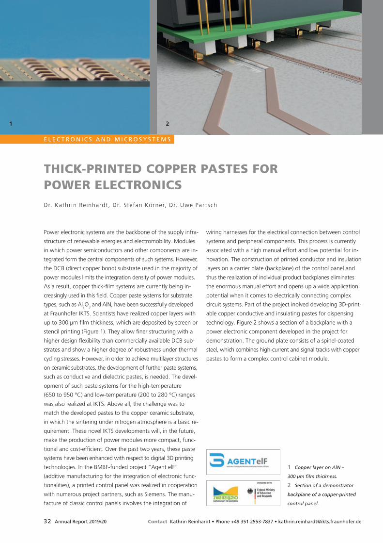
2 Section of a demonstrator
backplane of a copper-printed
control panel.
Dr. Kathr in Reinhardt , Dr. Stefan Körner, Dr. Uwe Par t sch
THICK-PRINTED COPPER PASTES FOR POWER ELECTRONICS
Contact Kathrin Reinhardt • Phone +49 351 2553-7837 • [email protected]
21
E L E C T R O N I C S A N D M I C R O S Y S T E M S
wiring harnesses for the electrical connection between control
systems and peripheral components. This process is currently
associated with a high manual effort and low potential for in-
novation. The construction of printed conductor and insulation
layers on a carrier plate (backplane) of the control panel and
thus the realization of individual product backplanes eliminates
the enormous manual effort and opens up a wide application
potential when it comes to electrically connecting complex
circuit systems. Part of the project inolved developing 3D-print-
able copper conductive and insulating pastes for dispensing
technology. Figure 2 shows a section of a backplane with a
power electronic component developed in the project for
demonstration. The ground plate consists of a spinel-coated
steel, which combines high-current and signal tracks with copper
pastes to form a complex control cabinet module.