Embed Size (px)
Citation preview

TL05x, TL05xAENHANCED-JFET LOW-OFFSET
OPERATIONAL AMPLIFIERS
SLOS178A – FEBRUARY 1997 - REVISED FEBRUARY 2003
1POST OFFICE BOX 655303 • DALLAS, TEXAS 75265
Direct Upgrades to TL07x and TL08x BiFETOperational Amplifiers
Faster Slew Rate (20 V/µs Typ) WithoutIncreased Power Consumption
On-Chip Offset-Voltage Trimming forImproved DC Performance and PrecisionGrades Are Available (1.5 mV, TL051A)
1
2
3
4
5
6
7
14
13
12
11
10
9
8
1OUT1IN–1IN+
VCC+2IN+2IN–
2OUT
4OUT4IN–4IN+VCC–3IN+3IN–3OUT
1
2
3
4
8
7
6
5
OFFSET N1IN–
IN+VCC–
NCVCC+OUTOFFSET N2
1
2
3
4
8
7
6
5
1OUT1IN–1IN+
VCC–
VCC+2OUT2IN–2IN+
TL054D, DB, N, OR NS PACKAGE
(TOP VIEW)
TL051D OR P PACKAGE
(TOP VIEW)
TL052D, P, OR PS PACKAGE
(TOP VIEW)
description/ordering information
The TL05x series of JFET-input operational amplifiers offers improved dc and ac characteristics over the TL07xand TL08x families of BiFET operational amplifiers. On-chip Zener trimming of offset voltage yields precisiongrades as low as 1.5 mV (TL051A) for greater accuracy in dc-coupled applications. Texas Instruments improvedBiFET process and optimized designs also yield improved bandwidth and slew rate without increased powerconsumption. The TL05x devices are pin-compatible with the TL07x and TL08x and can be used to upgradeexisting circuits or for optimal performance in new designs.
BiFET operational amplifiers offer the inherently higher input impedance of the JFET-input transistors, withoutsacrificing the output drive associated with bipolar amplifiers. This makes them better suited for interfacing withhigh-impedance sensors or very low-level ac signals. They also feature inherently better ac response thanbipolar or CMOS devices having comparable power consumption.
The TL05x family was designed to offer higher precision and better ac response than the TL08x, with the lownoise floor of the TL07x. Designers requiring significantly faster ac response or ensured lower noise shouldconsider the Excalibur TLE208x and TLE207x families of BiFET operational amplifiers.
Because BiFET operational amplifiers are designed for use with dual power supplies, care must be taken toobserve common-mode input voltage limits and output swing when operating from a single supply. DC biasingof the input signal is required, and loads should be terminated to a virtual-ground node at mid-supply. TexasInstruments TLE2426 integrated virtual ground generator is useful when operating BiFET amplifiers from singlesupplies.
The TL05x are fully specified at ±15 V and ±5 V. For operation in low-voltage and/or single-supply systems,Texas Instruments LinCMOS families of operational amplifiers (TLC-prefix) are recommended. When movingfrom BiFET to CMOS amplifiers, particular attention should be paid to the slew rate and bandwidthrequirements, and also the output loading.
Please be aware that an important notice concerning availability, standard warranty, and use in critical applications ofTexas Instruments semiconductor products and disclaimers thereto appears at the end of this data sheet.
Copyright 2003, Texas Instruments IncorporatedPRODUCTION DATA information is current as of publication date.Products conform to specifications per the terms of Texas Instrumentsstandard warranty. Production processing does not necessarily includetesting of all parameters.

TL05x, TL05xAENHANCED-JFET LOW-OFFSETOPERATIONAL AMPLIFIERS
SLOS178A – FEBRUARY 1997 - REVISED FEBRUARY 2003
2 POST OFFICE BOX 655303 • DALLAS, TEXAS 75265
ORDERING INFORMATION
TAVIOmaxAT 25°C PACKAGE† ORDERABLE
PART NUMBERTOP-SIDEMARKING
PDIP (P) Tube of 50TL051ACP TL051ACP
PDIP (P) Tube of 50TL052ACP TL052ACP
800 µV Tube of 75 TL051ACD 051AC
SOIC (D) Tube of 75 TL052ACD052AC
Reel of 2500 TL052ACDR052AC
PDIP (P) Tube of 50TL051CP TL051CP
PDIP (P) Tube of 50TL052CP TL052CP
PDIP (N) Tube of 25 TL054ACN TL054ACN
Tube of 75 TL051CDTL051C
0°C to 70°CReel of 2500 TL051CDR
TL051C
0°C to 70°C1.5 mV
SOIC (D)Tube of 75 TL052CD
TL052CSOIC (D)Reel of 2500 TL052CDR
TL052C
Tube of 50 TL054ACDTL054C
Reel of 2500 TL054ACDRTL054C
SOP (PS) Reel of 2000 TL052CPSR TL052
SSOP (DB) Reel of 2000 TL054CDBR TL054
PDIP (N) Tube of 25 TL054CN TL054CN
4 mV SOIC (D)Tube of 50 TL054CD
TL054C4 mV SOIC (D)Reel of 2500 TL054CDR
TL054C
SOP (NS) Reel of 2000 TL054CNSR TL054
PDIP (P) Tube of 50 TL052AIP TL052AI
800 µVSOIC (D)
Tube of 75 TL052AID052AISOIC (D)
Reel of 2500 TL052AIDR052AI
PDIP (N) Tube of 25 TL054AIN TL054AIN
PDIP (P) Tube of 50TL051IP TL051IP
PDIP (P) Tube of 50TL052IP TL052IP
40°C to 85°C 1 5 mVTube of 75 TL051ID TL051I
–40°C to 85°C 1.5 mVTube of 75 TL052ID
TL052ISOIC (D) Reel of 2500 TL052IDR
TL052I
Tube of 50 TL054AIDTL054AI
Reel of 2500 TL054AIDRTL054AI
PDIP (N) Tube of 25 TL054IN TL054IN
4 mVSOIC (D)
Tube of 50 TL054IDTL054ISOIC (D)
Reel of 2500 TL054IDRTL054I
† Package drawings, standard packing quantities, thermal data, symbolization, and PCB design guidelines are available atwww.ti.com/sc/package.

TL05x, TL05xAENHANCED-JFET LOW-OFFSET
OPERATIONAL AMPLIFIERS
SLOS178A – FEBRUARY 1997 - REVISED FEBRUARY 2003
3POST OFFICE BOX 655303 • DALLAS, TEXAS 75265
symbol (each amplifier)
+
–IN–
IN+OUT
equivalent schematic (each amplifier)
R9
OFFSET N2OFFSET N1
IN–
IN+
Q2
Q3Q7
VCC+
Q14
Q6
R4
Q8
Q10
R7
Q11
R6
C1
Q9Q5
Q4
R5
R1
Q1
JF1 JF2
Q13
Q16
R8
JF3Q15
Q17
OUT
VCC–
R2 R3
Q12
R10 D2
D1
See Note A
NOTE A: OFFSET N1 and OFFSET N2 are available only on the TL051x.
ACTUAL DEVICE COMPONENT COUNT†
COMPONENT TL051 TL052 TL054
Transistors 20 34 62
Resistors 10 19 37
Diodes 2 3 5
Capacitors 1 2 4
† These figures include all four amplifiers and all ESD, bias, and trim circuitry.

TL05x, TL05xAENHANCED-JFET LOW-OFFSETOPERATIONAL AMPLIFIERS
SLOS178A – FEBRUARY 1997 - REVISED FEBRUARY 2003
4 POST OFFICE BOX 655303 • DALLAS, TEXAS 75265
absolute maximum ratings over operating free-air temperature range (unless otherwise noted)†
Supply voltage, VCC+ (see Note 1) 18 V. . . . . . . . . . . . . . . . . . . . . . . . . . . . . . . . . . . . . . . . . . . . . . . . . . . . . . . . . . . Supply voltage, VCC– (see Note 1) –18 V. . . . . . . . . . . . . . . . . . . . . . . . . . . . . . . . . . . . . . . . . . . . . . . . . . . . . . . . . . Differential input voltage (see Note 2) ±30 V. . . . . . . . . . . . . . . . . . . . . . . . . . . . . . . . . . . . . . . . . . . . . . . . . . . . . . . . Input voltage range, VI (any input, see Notes 1 and 3) ±15 V. . . . . . . . . . . . . . . . . . . . . . . . . . . . . . . . . . . . . . . . . Input current, II (each input) ±1 mA. . . . . . . . . . . . . . . . . . . . . . . . . . . . . . . . . . . . . . . . . . . . . . . . . . . . . . . . . . . . . . . Output current, IO (each output) ±80 mA. . . . . . . . . . . . . . . . . . . . . . . . . . . . . . . . . . . . . . . . . . . . . . . . . . . . . . . . . . Total current into VCC+ 160 mA. . . . . . . . . . . . . . . . . . . . . . . . . . . . . . . . . . . . . . . . . . . . . . . . . . . . . . . . . . . . . . . . . . Total current out of VCC– 160 mA. . . . . . . . . . . . . . . . . . . . . . . . . . . . . . . . . . . . . . . . . . . . . . . . . . . . . . . . . . . . . . . . . Duration of short-circuit current at (or below) 25°C Unlimited. . . . . . . . . . . . . . . . . . . . . . . . . . . . . . . . . . . . . . . . . Package thermal impedance, θJA (see Notes 4 and 5): D package (8 pin) 97°C/W. . . . . . . . . . . . . . . . . . . . . .
D package (14 pin) 86°C/W. . . . . . . . . . . . . . . . . . . . . DB package (14 pin) 96°C/W. . . . . . . . . . . . . . . . . . . N package (14 pin) 80°C/W. . . . . . . . . . . . . . . . . . . . . NS package (14 pin) 76°C/W. . . . . . . . . . . . . . . . . . . P package (8 pin) 85°C/W. . . . . . . . . . . . . . . . . . . . . . PS package (8 pin) 95°C/W. . . . . . . . . . . . . . . . . . . .
Operating virtual junction temperature, TJ 150°C. . . . . . . . . . . . . . . . . . . . . . . . . . . . . . . . . . . . . . . . . . . . . . . . . . . Lead temperature 1,6 mm (1/16inch) from case for 10 seconds 260°C. . . . . . . . . . . . . . . . . . . . . . . . . . . . . . . . Storage temperature range –65°C to 150°C. . . . . . . . . . . . . . . . . . . . . . . . . . . . . . . . . . . . . . . . . . . . . . . . . . . . . . . .
† Stresses beyond those listed under “absolute maximum ratings” may cause permanent damage to the device. These are stress ratings only, andfunctional operation of the device at these or any other conditions beyond those indicated under “recommended operating conditions” is notimplied. Exposure to absolute-maximum-rated conditions for extended periods may affect device reliability.
NOTES: 1. All voltage values, except differential voltages, are with respect to the midpoint between VCC+ and VCC–.2. Differential voltages are at IN+ with respect to IN–.3. The magnitude of the input voltage must never exceed the magnitude of the supply voltage or 15 V, whichever is less.4. Maximum power dissipation is a function of TJ(max), θJA, and TA. The maximum allowable power dissipation at any allowable
ambient temperature is PD = (TJ(max) – TA)/θJA. Operating at the absolute maximum TJ of 150°C can impact reliability.5. The package thermal impedance is calculated in accordance with JESD 51-7.
recommended operating conditionsC SUFFIX I SUFFIX
UNITMIN MAX MIN MAX
UNIT
VCC± Supply voltage ±5 ±15 ±5 ±15 V
VIC Common mode input voltageVCC± = ±5 V –1 4 –1 4
VVIC Common-mode input voltageVCC± = ±15 V –11 11 –11 11
V
TA Operating free-air temperature 0 70 –40 85 °C

TL05x, TL05xAENHANCED-JFET LOW-OFFSET
OPERATIONAL AMPLIFIERS
SLOS178A – FEBRUARY 1997 - REVISED FEBRUARY 2003
5POST OFFICE BOX 655303 • DALLAS, TEXAS 75265
TL051C and TL051AC electrical characteristics at specified free-air temperature
†TL051C, TL051AC
PARAMETER TEST CONDITIONS TA† VCC± = ±5 V VCC± = ±15 V UNIT
MIN TYP MAX MIN TYP MAX
TL051C25°C 0.75 3.5 0.59 1.5
VIO Input offset voltage
TL051CFull range 4.5 2.5
mVVIO Input offset voltage
TL051AC25°C 0.55 2.8 0.35 0.8
mV
VO = 0
TL051ACFull range 3.8 1.8
Temperature coefficient
VO = 0,VIC = 0,RS = 50 Ω
TL051C25°C to70°C 8 8
µV/°CVIO of input offset voltage‡RS = 50 Ω
TL051AC25°C to70°C 8 8 25
µV/°C
Input offset-voltage long-term drift§
25°C 0.04 0.04 µV/mo
IIO Input offset currentVO = 0, VIC = 0, 25°C 4 100 5 100 pA
IIO Input offset current O ICSee Figure 5 70°C 0.02 1 0.025 1 nA
IIB Input bias currentVO = 0, VIC = 0, 25°C 20 200 30 200 pA
IIB Input bias current O ICSee Figure 5 70°C 0.15 4 0.2 4 nA
VICRCommon-mode input
25°C–1to4
–2.3to
5.6
–11to11
–12.3to
15.6VVICR voltage range
Full range–1to 4
–11to11
V
RL = 10 kΩ25°C 3 4.2 13 13.9
VOMMaximum positive peak
RL = 10 kΩFull range 3 13
VVOM+ output voltage swingRL = 2 kΩ
25°C 2.5 3.8 11.5 12.7V
RL = 2 kΩFull range 2.5 11.5
RL = 10 kΩ25°C –2.5 –3.5 –12 –13.2
VOMMaximum negative peak
RL = 10 kΩFull range –2.5 –12
VVOM–g
output voltage swingRL = 2 kΩ
25°C –2.3 –3.2 –11 –12V
RL = 2 kΩFull range –2.3 –11
L i l diff ti l25°C 25 59 50 105
AVDLarge-signal differentialvoltage amplification¶ RL = 2 kΩ 0°C 30 65 60 129 V/mVvoltage am lification¶
70°C 20 46 30 85
ri Input resistance 25°C 1012 1012 Ωci Input capacitance 25°C 10 12 pF
Common mode V V min25°C 65 85 75 93
CMRRCommon-moderejection ratio
VIC = VICRmin,VO = 0 RS = 50 Ω 0°C 65 84 75 92 dB
rejection ratio VO = 0, RS = 50 Ω70°C 65 84 75 91
Supply voltage rejection25°C 75 99 75 99
kSVRSupply-voltage rejectionratio (∆VCC±/∆VIO)
VO = 0, RS = 50 Ω 0°C 75 98 75 98 dBratio (∆VCC±/∆VIO)
70°C 75 97 75 97
25°C 2.6 3.2 2.7 3.2
ICC Supply current VO = 0, No load 0°C 2.7 3.2 2.8 3.2 mACC y O70°C 2.6 3.2 2.7 3.2
† Full range is 0°C to 70°C.‡ This parameter is tested on a sample basis for the TL051A. For other test requirements, please contact the factory. This statement has no bearing
on testing or nontesting of other parameters.§ Typical values are based on the input offset-voltage shift observed through 168 hours of operating life test at TA = 150°C, extrapolated to
TA = 25°C using the Arrhenius equation, and assuming an activation energy of 0.96 eV.¶ For VCC± = ±5 V, VO = ±2.3 V, or for VCC± = ±15 V, VO = ±10 V.

TL05x, TL05xAENHANCED-JFET LOW-OFFSETOPERATIONAL AMPLIFIERS
SLOS178A – FEBRUARY 1997 - REVISED FEBRUARY 2003
6 POST OFFICE BOX 655303 • DALLAS, TEXAS 75265
TL051C and TL051AC operating characteristics at specified free-air temperature
†TL051C, TL051AC
PARAMETER TEST CONDITIONS TA† VCC± = ±5 V VCC± = ±15 V UNIT
MIN TYP MAX MIN TYP MAX
P iti l t25°C 16 13 20
SR+ Positive slew rateat unity gain‡
RL = 2 kΩ, CL = 100 pF,
Fullrange
16.4 11 22.6
V/µs
N ti l t
L , L ,See Figure 1 25°C 15 13 18
V/µs
SR– Negative slew rateat unity gain‡ Full
range16 11 19.3
25°C 55 56
tr Rise time 0°C 54 55
70°C 63 63ns
VI(PP) = ±10 mV,R 2 kΩ
25°C 55 57ns
tf Fall timeRL = 2 kΩ,CL = 100 pF
0°C 54 56CL = 100 F,See Figures 1 and 2 70°C 62 64g
25°C 24 19
Overshoot factor 0°C 24 19 %
70°C 24 19
VEquivalent input noise f = 10 Hz 25°C 75 75
nV/√HzVnq
voltage§ RS = 20 Ω, f = 1 kHz 25°C 18 18 30nV/√Hz
VN(PP)Peak-to-peak equivalent input noise voltage
See Figure 3 f = 10 Hz to10 kHz
25°C 4 4 µV
InEquivalent inputnoise current
f = 1 kHz 25°C 0.01 0.01 pA/√Hz
THD Total harmonic distortion¶ RS = 1 kΩ,f = 1 kHz
RL = 2 kΩ,25°C 0.003 0.003 %
V 10 V R 2 kΩ25°C 3 3.1
B1 Unity-gain bandwidthVI = 10 mV, RL = 2 kΩ,CL = 25 pF See Figure 4
0°C 3.2 3.3 MHzCL = 25 F, See Figure 4
70°C 2.7 2.8
Phase margin at unity V 10 mV R 2 kΩ25°C 59 62
φmPhase margin at unitygain
VI = 10 mV, RL = 2 kΩ,CL = 25 pF, See Figure 4 0°C 58 62 deggain CL = 25 F, See Figure 4
70°C 59 62
† Full range is 0°C to 70°C.‡ For VCC± = ±5 V, VI(PP) = ±1 V; for VCC± = ±15 V, VI(PP) = ±5 V.§ This parameter is tested on a sample basis for the TL051A. For other test requirements, please contact the factory. This statement has no bearing
on testing or nontesting of other parameters.¶ For VCC± = ±5 V, VO(RMS) = 1 V; for VCC± = ±15 V, VO(RMS) = 6 V.

TL05x, TL05xAENHANCED-JFET LOW-OFFSET
OPERATIONAL AMPLIFIERS
SLOS178A – FEBRUARY 1997 - REVISED FEBRUARY 2003
7POST OFFICE BOX 655303 • DALLAS, TEXAS 75265
TL051I and TL051AI electrical characteristics at specified free-air temperature
†
TL051I, TL051AI
PARAMETER TEST CONDITIONS TA† VCC± = ±5 V VCC± = ±15 V UNITAMIN TYP MAX MIN TYP MAX
TL051I25°C 0.75 3.5 0.59 1.5
VIO Input offset voltage
TL051IFull range 5.3 3.3
mVVIO Input offset voltage
TL051AI25°C 0.55 2.8 0.35 0.8
mV
VO = 0
TL051AIFull range 4.6 2.6
Temperature coefficient of
VO = 0,VIC = 0,RS = 50 Ω
TL051I25°C to85°C 7 8
µV/°CVIO input offset voltage‡RS = 50 Ω
TL051AI25°C to85°C 8 8 25
µV/°C
Input offset-voltage long-term drift§
25°C 0.04 0.04 µV/mo
IIO Input offset currentVO = 0, VIC = 0, 25°C 4 100 5 100 pA
IIO Input offset current O ICSee Figure 5 85°C 0.06 10 0.07 10 nA
IIB Input bias currentVO = 0, VIC = 0, 25°C 20 200 30 200 pA
IIB Input bias current O ICSee Figure 5 85°C 0.6 20 0.7 20 nA
VICRCommon-mode input
25°C–1to4
–2.3to
5.6
–11to11
–12.3to
15.6VVICR voltage range
Full range–1to4
–11to11
V
RL = 10 kΩ25°C 3 4.2 13 13.9
VOMMaximum positive peak
RL = 10 kΩFull range 3 13
VVOM + output voltage swingRL = 2 kΩ
25°C 2.5 3.8 11.5 12.7V
RL = 2 kΩFull range 2.5 11.5
RL = 10 kΩ25°C –2.5 –3.5 –12 –13.2
VOMMaximum negative peak
RL = 10 kΩFull range –2.5 –12
VVOM –g
output voltage swingRL = 2 kΩ
25°C –2.3 –3.2 –11 –12V
RL = 2 kΩFull range –2.3 –11
L i l diff ti l25°C 25 59 50 105
AVDLarge-signal differentialvoltage amplification¶ RL = 2 kΩ –40°C 30 74 60 145 V/mVvoltage am lification¶
85°C 20 43 30 76
ri Input resistance 25°C 1012 1012 Ωci Input capacitance 25°C 10 12 pF
Common modeVIC = VICRmin, 25°C 65 85 75 93
CMRRCommon-moderejection ratio
VIC VICRmin,VO = 0, –40°C 65 83 75 90 dB
rejection ratioRS = 50 Ω 85°C 65 84 75 93
Supply voltage rejection V 025°C 75 99 75 99
kSVRSupply-voltage rejectionratio (∆VCC±/∆VIO)
VO = 0,RS = 50 Ω
–40°C 75 98 75 98 dBratio (∆VCC±/∆VIO) RS = 50 Ω
85°C 75 99 75 99
25°C 2.6 3.2 2.7 3.2
ICC Supply current VO = 0, No load –40°C 2.4 3.2 2.6 3.2 mA
85°C 2.5 3.2 2.6 3.2
† Full range is –40°C to 85°C‡ This parameter is tested on a sample basis for the TL051A. For other test requirements, please contact the factory. This statement has no bearing
on testing or nontesting of other parameters.§ Typical values are based on the input offset-voltage shift observed through 168 hours of operating life test at TA = 150°C, extrapolated to
TA = 25°C using the Arrhenius equation, and assuming an activation energy of 0.96 eV.¶ For VCC± = ±5 V, VO = ±2.3 V, or for VCC± = ±15 V, VO = ±10 V.

TL05x, TL05xAENHANCED-JFET LOW-OFFSETOPERATIONAL AMPLIFIERS
SLOS178A – FEBRUARY 1997 - REVISED FEBRUARY 2003
8 POST OFFICE BOX 655303 • DALLAS, TEXAS 75265
TL051I and TL051AI operating characteristics at specified free-air temperature
†TL051I, TL051AI
PARAMETER TEST CONDITIONS TA† VCC± = ±5 V VCC± = ±15 V UNIT
MIN TYP MAX MIN TYP MAX
P iti l t25°C 16 13 20
SR+ Positive slew rateat unity gain‡
RL = 2 kΩ, CL = 100 pF,
Fullrange
11
V/µs
N ti l t
L , L ,See Figure 1 25°C 15 13 18
V/µs
SR– Negative slew rateat unity gain‡ Full
range11
25°C 55 56
tr Rise time –40°C 52 53
85°C 64 65ns
VI(PP) = ±10 mV,R 2 kΩ
25°C 55 57ns
tf Fall time
( )RL = 2 kΩ,CL = 100 pF
–40°C 51 53CL = 100 F,See Figures 1 and 2 85°C 64 65g
25°C 24 19
Overshoot factor –40°C 24 19 %
85°C 24 19
V Equivalent input noise f = 10 Hz 25°C 75 75nV/√HzVn
qvoltage§ RS = 20 Ω, f = 1 kHz 25°C 18 18 30
nV/√Hz
VN(PP)Peak-to-peak equivalent input noise voltage
See Figure 3 f = 10 Hz to10 kHz
25°C 4 4 µV
InEquivalent inputnoise current
f = 1 kHz 25°C 0.01 0.01 pA/√Hz
THD Total harmonic distortion¶ RS = 1 kΩ,f = 1 kHz
RL = 2 kΩ,25°C 0.003 0.003 %
V 10 V R 2 kΩ25°C 3 3.1
B1 Unity-gain bandwidthVI = 10 mV, RL = 2 kΩ,CL = 25 pF See Figure 4
–40°C 3.5 3.6 MHzCL = 25 F, See Figure 4
85°C 2.6 2.7
Phase margin at unity V 10 mV R 2 kΩ25°C 59 62
φmPhase margin at unitygain
VI = 10 mV, RL = 2 kΩ,CL = 25 pF, See Figure 4 –40°C 58 61 deggain CL = 25 F, See Figure 4
85°C 59 62
† Full range is –40°C to 85°C.‡ For VCC± = ±5 V, VI(PP) = ±1 V; for VCC± = ±15 V, VI(PP) = ±5 V.§ This parameter is tested on a sample basis for the TL051A. For other test requirements, please contact the factory. This statement has no bearing
on testing or nontesting of other parameters.¶ For VCC± = ±5 V, VO(RMS) = 1 V; for VCC± = ±15 V, VO(RMS) = 6 V.

TL05x, TL05xAENHANCED-JFET LOW-OFFSET
OPERATIONAL AMPLIFIERS
SLOS178A – FEBRUARY 1997 - REVISED FEBRUARY 2003
9POST OFFICE BOX 655303 • DALLAS, TEXAS 75265
TL052C and TL052AC electrical characteristics at specified free-air temperature
TL052C, TL052AC
PARAMETER TEST CONDITIONS TA† VCC± = ±5 V VCC± = ±15 V UNITAMIN TYP MAX MIN TYP MAX
TL052C25°C 0.73 3.5 0.65 1.5
VIO Input offset voltage
TL052CFull range 4.5 2.5
mVVIO Input offset voltage
V 0 TL052AC25°C 0.51 2.8 0.4 0.8
mV
VO = 0,VIC = 0
TL052ACFull range 3.8 1.8
VIC = 0,RS = 50 Ω TL052C
25°C to8 8
Temperature coefficient
RS 50 Ω TL052C70°C 8 8
µV/°CVIO of input offset voltage‡TL052AC
25°C to8 6 25
µV/°CTL052AC
70°C 8 6 25
Input offset-voltage long-term drift§
VO = 0,RS = 50 Ω VIC = 0, 25°C 0.04 0.04 µV/mo
IIO Input offset currentVO = 0,
VIC = 025°C 4 100 5 100 pA
IIO Input offset current O ,See Figure 5
VIC = 0,70°C 0.02 1 0.025 1 nA
IIB Input bias currentVO = 0,
VIC = 025°C 20 200 30 200 pA
IIB Input bias current O ,See Figure 5
VIC = 0,70°C 0.15 4 0.2 4 nA
VICRCommon-mode input
25°C–1to4
–2.3to
5.6
–11to11
–12.3to
15.6VVICR voltage range
Full range–1to4
–11to11
V
RL = 10 kΩ25°C 3 4.2 13 13.9
VOMMaximum positive peak
RL = 10 kΩFull range 3 13
VVOM+ output voltage swingRL = 2 kΩ
25°C 2.5 3.8 11.5 12.7V
RL = 2 kΩFull range 2.5 11.5
RL = 10 kΩ25°C –2.5 –3.5 –12 –13.2
VOMMaximum negative peak
RL = 10 kΩFull range –2.5 –12
VVOM–g
output voltage swingRL = 2 kΩ
25°C –2.3 –3.2 –11 –12V
RL = 2 kΩFull range –2.3 –11
L i l diff ti l25°C 25 59 50 105
AVDLarge-signal differentialvoltage amplification¶ RL = 2 kΩ 0°C 30 65 60 129 V/mVvoltage am lification¶
70°C 20 46 30 85
ri Input resistance 25°C 1012 1012 Ω
ci Input capacitance 25°C 10 12 pF
Common mode V V min25°C 65 85 75 93
CMRRCommon-moderejection ratio
VIC = VICRmin,VO = 0, RS = 50 Ω 0°C 65 84 75 92 dBrejection ratio VO = 0,
70°C 65 84 75 91† Full range is 0°C to 70°C.‡ This parameter is tested on a sample basis. For other test requirements, please contact the factory. This statement has no bearing on testing
or nontesting of other parameters.§ Typical values are based on the input offset-voltage shift observed through 168 hours of operating life test at TA = 150°C, extrapolated to
TA = 25°C using the Arrhenius equation, and assuming an activation energy of 0.96 eV.¶ For VCC± = ±5 V, VO = ±2.3 V; at VCC± = ±15 V, VO = ±10 V.

TL05x, TL05xAENHANCED-JFET LOW-OFFSETOPERATIONAL AMPLIFIERS
SLOS178A – FEBRUARY 1997 - REVISED FEBRUARY 2003
10 POST OFFICE BOX 655303 • DALLAS, TEXAS 75265
TL052C and TL052AC electrical characteristics at specified free-air temperature (continued)
TL052C, TL052AC
PARAMETER TEST CONDITIONS TA VCC± = ±5 V VCC± = ±15 V UNITAMIN TYP MAX MIN TYP MAX
S l lt j ti25°C 75 99 75 99
kSVRSupply-voltage rejectionratio (∆VCC±/∆VIO)
VO = 0, RS = 50 Ω 0°C 75 98 75 98 dBratio (∆VCC±/∆VIO)
70°C 75 97 75 97
S l t25°C 4.6 5.6 4.8 5.6
ICCSupply current(two amplifiers)
VO = 0, No load 0°C 4.7 6.4 4.8 6.4 mA(two am lifiers)
70°C 4.4 6.4 4.6 6.4
VO1/VO2 Crosstalk attenuation AVD = 100 25°C 120 120 dB
TL052C and TL052AC operating characteristics at specified free-air temperature
TL052C, TL052AC
PARAMETER TEST CONDITIONS TA† VCC± = ±5 V VCC± = ±15 V UNITAMIN TYP MAX MIN TYP MAX
SR+ Slew rate at unity gain25°C 17.8 9 20.7
SR+ Slew rate at unity gainRL = 2 kΩ, CL = 100 pF, Full range 8
V/µs
SR Negative slew rate See Figure 1 25°C 15.4 9 17.8V/µs
SR– gat unity gain‡ Full range 8
25°C 55 56
tr Rise time 0°C 54 55
70°C 63 63ns
VI(PP) = ±10 mV,R 2 kΩ
25°C 55 57ns
tf Fall time
( )RL = 2 kΩ,CL = 100 pF
0°C 54 56CL = 100 F,See Figures 1 and 2 70°C 62 64g
25°C 24 19
Overshoot factor 0°C 24 19 %
70°C 24 19
V Equivalent input noise f = 10 Hz 25°C 71 71nV/√HzVn
qvoltage§ RS = 20 Ω, f = 1 kHz 25°C 19 19 30
nV/√Hz
VN(PP)Peak-to-peak equivalent input noise current
See Figure 3 f = 10 Hz to10 kHz
25°C 4 4 µV
InEquivalent input noise current
f = 1 kHz 25°C 0.01 0.01 pA/√Hz
THD Total harmonic distortion¶ RS = 1 kΩ,f = 1 kHz
RL = 2 kΩ,25°C 0.003 0.003 %
V 10 V R 2 kΩ25°C 3 3
B1 Unity-gain bandwidthVI = 10 mV,CL = 25 pF
RL = 2 kΩ,See Figure 4
0°C 3.2 3.2 MHzCL = 25 F, See Figure 4
70°C 2.6 2.7
Phase margin at unity V 10 mV R 2 kΩ25°C 60 63
φmPhase margin at unitygain
VI = 10 mV,CL = 25 pF,
RL = 2 kΩ,See Figure 4 0°C 59 63 deggain CL = 25 F, See Figure 4
70°C 60 63† Full range is 0°C to 70°C.‡ For VCC± = ±5 V, VI(PP) = ±1 V; for VCC± = ±15 V, VI(PP) = ±5 V.§ This parameter is tested on a sample basis. For other test requirements, please contact the factory. This statement has no bearing on testing
or nontesting of other parameters.¶ For VCC± = ±5 V, VO(RMS) = 1 V; for VCC± = ±15 V, VO(RMS) = 6 V.

TL05x, TL05xAENHANCED-JFET LOW-OFFSET
OPERATIONAL AMPLIFIERS
SLOS178A – FEBRUARY 1997 - REVISED FEBRUARY 2003
11POST OFFICE BOX 655303 • DALLAS, TEXAS 75265
TL052I and TL052AI electrical characteristics at specified free-air temperature
TL052I, TL052AI
PARAMETER TEST CONDITIONS TA† VCC± = ±5 V VCC± = ±15 V UNITAMIN TYP MAX MIN TYP MAX
TL052I25°C 0.73 3.5 0.65 1.5
VIO Input offset voltage
TL052IFull range 5.3 3.3
mVVIO Input offset voltage
V 0 TL052AI25°C 0.51 2.8 0.4 0.8
mV
VO = 0,VIC = 0,
TL052AIFull range 4.6 2.6
T t ffi i t‡
VIC = 0,RS = 50 Ω
TL052I25°C to85°C 7 6
µV/°CVIOTemperature coefficient‡
TL052AI25°C to85°C 6 6 25
µV/°C
Input offset-voltage long-term drift§
VO = 0,RS = 50 Ω VIC = 0, 25°C 0.04 0.04 µV/mo
IIO Input offset currentVO = 0, VIC = 0, 25°C 4 100 5 100 pA
IIO Input offset current O ,See Figure 5
IC ,
85°C 0.06 10 0.07 10 nA
IIB Input bias currentVO = 0, VIC = 0, 25°C 20 200 30 200 pA
IIB Input bias current O ,See Figure 5
IC ,
85°C 0.6 20 0.7 20 nA
VICRCommon-mode input
25°C–1to4
–2.3to
5.6
–11to11
–12.3to
15.6VVICR voltage range
Full range–1to4
–11to11
V
RL = 10 kΩ25°C 3 4.2 13 13.9
VOMMaximum positive peak
RL = 10 kΩFull range 3 13
VVOM+ output voltage swingRL = 2 kΩ
25°C 2.5 3.8 11.5 12.7V
RL = 2 kΩFull range 2.5 11.5
RL = 10 kΩ25°C –2.5 –3.5 –12 –13.2
VOMMaximum negative peak
RL = 10 kΩFull range –2.5 –12
VVOM–g
output voltage swingRL = 2 kΩ
25°C –2.3 –3.2 –11 –12V
RL = 2 kΩFull range –2.3 –11
L i l diff ti l25°C 25 59 50 105
AVDLarge-signal differentialvoltage amplification¶ RL = 2 kΩ –40°C 30 74 60 145 V/mVvoltage am lification¶
85°C 20 43 30 76
ri Input resistance 25°C 1012 1012 Ω
ci Input capacitance 25°C 10 12 pF
Common mode V V min25°C 65 85 75 93
CMRRCommon-moderejection ratio
VIC = VICRmin,VO = 0, RS = 50 Ω –40°C 65 83 75 90 dBrejection ratio VO = 0,
85°C 65 84 75 93
† Full range is –40°C to 85°C.‡ This parameter is tested on a sample basis. For other test requirements, please contact the factory. This statement has no bearing on testing
or nontesting of other parameters§ Typical values are based on the input offset-voltage shift observed through 168 hours of operating life test at TA = 150°C, extrapolated to
TA = 25°C using the Arrhenius equation, and assuming an activation energy of 0.96 eV.¶ At VCC± = ±5 V, VO = ±2.3 V; at VCC± = ±15 V, VO = ±10 V.

TL05x, TL05xAENHANCED-JFET LOW-OFFSETOPERATIONAL AMPLIFIERS
SLOS178A – FEBRUARY 1997 - REVISED FEBRUARY 2003
12 POST OFFICE BOX 655303 • DALLAS, TEXAS 75265
TL052I and TL052AI electrical characteristics at specified free-air temperature (continued)
TL052I, TL052AI
PARAMETER TEST CONDITIONS TA VCC± = ±5 V VCC± = ±15 V UNITAMIN TYP MAX MIN TYP MAX
S l lt j ti25°C 75 99 75 99
kSVRSupply-voltage rejectionratio (∆VCC±/∆VIO)
VO = 0, RS = 50 Ω –40°C 75 98 75 98 dBratio (∆VCC±/∆VIO)
85°C 75 99 75 99
S l t25°C 4.6 5.6 4.8 5.6
ICCSupply current(two amplifiers)
VO = 0, No load –40°C 4.5 6.4 4.7 6.4 mA(two am lifiers)
85°C 4.4 6.4 4.6 6.4
VO1/VO2 Crosstalk attenuation AVD = 100 25°C 120 120 dB
TL052I and TL052AI operating characteristics at specified free-air temperature
TL052I, TL052AI
PARAMETER TEST CONDITIONS TA† VCC± = ±5 V VCC± = ±15 V UNITAMIN TYP MAX MIN TYP MAX
SR+ Sl t t it i ‡25°C 17.8 9 20.7
SR+ Slew rate at unity gain‡RL = 2 kΩ, CL = 100 pF, Full range 8
V/µs
SR Negative slew rate at
L , L ,See Figure 1 25°C 15.4 9 17.8
V/µs
SR– gunity gain‡ Full range 8
25°C 55 56
tr Rise time –40°C 52 53
85°C 64 65ns
VI(PP) = ±10 mV, 25°C 55 57ns
tf Fall timeVI(PP) = ±10 mV,RL = 2 kΩ, CL = 100 pF, –40°C 51 53See Figures 1 and 2 85°C 64 65
25°C 24% 19%
Overshoot factor –40°C 24% 19% %
85°C 24% 19
VEquivalent input noise f = 10 Hz 25°C 71 71
nV/√HzVnq
voltage§ RS = 20 Ω, f = 1 kHz 25°C 19 19 30nV/√Hz
VN(PP)Peak-to-peak equivalent input noise current
See Figure 3 f = 10 Hz to10 kHz
25°C 4 4 µV
InEquivalent input noisecurrent
f = 1 kHz 25°C 0.01 0.01 pA/√Hz
THD Total harmonic distortion¶ RS = 1 kΩ,f = 1 kHz
RL = 2 kΩ,25°C 0.003 0.003 %
V 10 V R 2 kΩ25°C 3 3
B1 Unity-gain bandwidthVI = 10 mV,CL = 25 pF
RL = 2 kΩ,See Figure 4
–40°C 3.5 3.6 MHzCL = 25 F, See Figure 4
85°C 2.5 2.6
Phase margin at unity V 10 mV R 2 kΩ25°C 60 63
φmPhase margin at unitygain
VI = 10 mV,CL = 25 pF,
RL = 2 kΩ,See Figure 4 –40°C 58 61 deggain CL = 25 F, See Figure 4
85°C 60 63† Full range is –40°C to 85°C.‡ For VCC± = ±5 V, VI(PP) = ±1 V; for VCC± = ±15 V, VI(PP) = ±5 V.§ This parameter is tested on a sample basis. For other test requirements, please contact the factory. This statement has no bearing on testing
or nontesting of other parameters.¶ For VCC± = ±5 V, VO(RMS) = 1 V; for VCC± = ±15 V, VO(RMS) = 6 V.

TL05x, TL05xAENHANCED-JFET LOW-OFFSET
OPERATIONAL AMPLIFIERS
SLOS178A – FEBRUARY 1997 - REVISED FEBRUARY 2003
13POST OFFICE BOX 655303 • DALLAS, TEXAS 75265
TL054C and TL054AC electrical characteristics at specified free-air temperature
†TL054C, TL054AC
PARAMETER TEST CONDITIONS TA† VCC± = ±5 V VCC± = ±15 V UNIT
MIN TYP MAX MIN TYP MAX
TL054C25°C 0.64 5.5 0.56 4
VIO Input offset voltage
TL054CFull range 7.7 6.2
mVVIO Input offset voltage
TL054AC25°C 0.57 3.5 0.5 1.5
mV
VO = 0TL054AC
Full range 5.7 3.7
Temperature coefficient
VO = 0,VIC = 0,RS = 50 Ω
TL054C25°C to70°C 25 23
µV/°CVIO of input offset voltageRS 50 Ω
TL054AC25°C to70°C 24 23
µV/°C
Input offset-voltage long-term drift‡
25°C 0.04 0.04 µV/mo
IIO Input offset currentVO = 0, VIC = 0, 25°C 4 100 5 100 pA
IIO Input offset current O ICSee Figure 5 70°C 0.02 1 0.025 1 nA
IIB Input bias currentVO = 0, VIC = 0, 25°C 20 200 30 200 pA
IIB Input bias current O ICSee Figure 5 70°C 0.15 4 0.2 4 nA
VICRCommon-mode input
25°C–1to4
–2.3to
5.6
–11to11
–12.3to
15.6VVICR voltage range
Full range–1to4
–11to11
V
RL = 10 kΩ25°C 3 4.2 13 13.9
VOMMaximum positive peak
RL = 10 kΩFull range 3 13
VVOM+ output voltage swingRL = 2 kΩ
25°C 2.5 3.8 11.5 12.7V
RL = 2 kΩFull range 2.5 11.5
RL = 10 kΩ25°C –2.5 –3.5 –12 –13.2
VOMMaximum negative peak
RL = 10 kΩFull range –2.5 –12
VVOM–g
output voltage swingRL = 2 kΩ
25°C –2.3 –3.2 –11 –12V
RL = 2 kΩFull range –2.3 –11
L i l diff ti l25°C 25 72 50 133
AVDLarge-signal differentialvoltage amplification§ RL = 2 kΩ 0°C 30 88 60 173 V/mVvoltage am lification§
70°C 20 57 30 85
ri Input resistance 25°C 1012 1012 Ωci Input capacitance 25°C 10 12 pF
Common mode V V min25°C 65 84 75 92
CMRRCommon-moderejection ratio
VIC = VICRmin,VO = 0 RS = 50 Ω
0°C 65 84 75 92 dBrejection ratio VO = 0, RS = 50 Ω
70°C 65 84 75 93
Supply voltage rejection V ±5 V to ±15 V25°C 75 99 75 99
kSVRSupply-voltage rejectionratio (∆VCC±/∆VIO)
VCC± = ±5 V to ±15 V,VO = 0 RS = 50 Ω
0°C 75 99 75 99 dBratio (∆VCC±/∆VIO) VO = 0, RS = 50 Ω
70°C 75 99 75 99
Supply current25°C 8.1 11.2 8.4 11.2
ICCSupply current(four amplifiers)
VO = 0, No load 0°C 8.2 12.8 8.5 12.8 mA(four am lifiers)
70°C 7.9 11.2 8.2 11.2
VO1/VO2 Crosstalk attenuation AVD = 100 25°C 120 120 dB
† Full range is 0°C to 70°C.‡ Typical values are based on the input offset-voltage shift observed through 168 hours of operating life test at TA = 150°C, extrapolated to
TA = 25°C using the Arrhenius equation, and assuming an activation energy of 0.96 eV.§ For VCC± = ±5 V, VO = ±2.3 V, at VCC± = ±15 V, VO = ±10 V.B

TL05x, TL05xAENHANCED-JFET LOW-OFFSETOPERATIONAL AMPLIFIERS
SLOS178A – FEBRUARY 1997 - REVISED FEBRUARY 2003
14 POST OFFICE BOX 655303 • DALLAS, TEXAS 75265
TL054C and TL054AC operating characteristics at specified free-air temperature
†TL054C, TL054C
PARAMETER TEST CONDITIONS TA† VCC± = ±5 V VCC± = ±15 V UNIT
MIN TYP MAX MIN TYP MAX
SR+Positive slew rate 25°C 15.4 10 17.8
SR+ at unity gain 0°C 15.7 8 17.9
RL = 2 kΩ, CL = 100 pF, 70°C 14.4 8 17.5V/µs
SR Negative slew rate at
L LSee Figure 1 and Note 7 25°C 13.9 10 15.9
V/µs
SR– gunity gain‡ 0°C 14.3 8 16.1
70°C 13.3 8 15.5
25°C 55 56
tr Rise time 0°C 54 55
70°C 63 63nsVI(PP) = ±10 mV,
R 2 kΩ25°C 55 57
ns
tf Fall timeRL = 2 kΩ,CL = 100 pF
0°C 54 56CL = 100 F,See Figures 1 and 2 70°C 62 64See Figures 1 and 2
25°C 24% 19%
Overshoot factor 0°C 24% 19% %
70°C 24% 19
V Equivalent input noise f = 10 Hz 25°C 75 75nV/√HzVn
qvoltage§ RS = 20 Ω, f = 1 kHz 25°C 21 21 45
nV/√Hz
VN(PP)Peak-to-peak equivalent input noise voltage
See Figure 3 f = 10 Hz to10 kHz
25°C 4 4 µV
InEquivalent inputnoise current
f = 1 kHz 25°C 0.01 0.01 pA/√Hz
THD Total harmonicdistortion¶
RS = 1 kΩ,f = 1 kHz
RL = 2 kΩ,25°C 0.003 0.003 %
V 10 mV R 2 kΩ25°C 2.7 2.7
B1 Unity-gain bandwidthVI = 10 mV, RL = 2 kΩ,CL = 25 pF See Figure 4
0°C 3 3 MHzCL = 25 F, See Figure 4
70°C 2.4 2.4
Phase margin at VI = 10 mV RL = 2 kΩ25°C 61 64
φmPhase margin atunity gain
VI = 10 mV, RL = 2 kΩ,CL = 25 pF See Figure 4 0°C 60 64 degunity gain CL = 25 F, See Figure 4
70°C 61 63
† Full range is 0°C to 70°C.‡ For VCC± = ±5 V, VI(PP) = ±1 V; for VCC± = ±15 V, VI(PP) = ±5 V.§ This parameter is tested on a sample basis. For other test requirements, please contact the factory. This statement has no bearing on testing
or nontesting of other parameters.¶ For VCC± = ±5 V, VO(RMS) = 1 V; for VCC± = ±15 V, VO(RMS) = 6 V.

TL05x, TL05xAENHANCED-JFET LOW-OFFSET
OPERATIONAL AMPLIFIERS
SLOS178A – FEBRUARY 1997 - REVISED FEBRUARY 2003
15POST OFFICE BOX 655303 • DALLAS, TEXAS 75265
TL054I and TL054AI electrical characteristics at specified free-air temperature
†TL054I, TL054AI
PARAMETER TEST CONDITIONS TA† VCC± = ±5 V VCC± = ±15 V UNITAMIN TYP MAX MIN TYP MAX
TL054I25°C 0.64 5.5 0.56 4
VIO Input offset voltage
TL054IFull range 8.8 7.3
mVVIO In ut offset voltage
TL054AI25°C 0.57 3.5 0.5 1.5
mV
VO = 0TL054AI
Full range 6.8 4.8
Temperature coefficient of
VO = 0,VIC = 0,RS = 50 Ω
TL054I25°C to85°C 25 24
µV/°CVIO input offset voltageRS 50 Ω
TL054AI25°C to85°C 25 23
µV/°C
Input offset voltage long-term drift‡
25°C 0.04 0.04 µV/mo
IIO Input offset currentVO = 0, VIC = 0, 25°C 4 100 5 100 pA
IIO Input offset current O ICSee Figure 5 85°C 0.06 10 0.07 10 nA
IIB Input bias currentVO = 0, VIC = 0, 25°C 20 200 30 200 pA
IIB Input bias current O ICSee Figure 5 85°C 0.6 20 0.7 20 nA
VICRCommon-mode input
25°C–1to4
–2.3to
5.6
–11to11
–12.3to
15.6VVICR voltage range
Full range–1to4
–11to11
V
RL = 10 kΩ25°C 3 4.2 13 13.9
VOMMaximum positive peak
RL = 10 kΩFull range 3 13
VVOM+ output voltage swingRL = 2 kΩ
25°C 2.5 3.8 11.5 12.7V
RL = 2 kΩFull range 2.5 11.5
RL = 10 kΩ25°C –2.5 –3.5 –12 –13.2
VOMMaximum negative peak
RL = 10 kΩFull range –2.5 –12
VVOM–g
output voltage swingRL = 2 kΩ
25°C –2.3 –3.2 –11 –12V
RL = 2 kΩFull range –2.3 –11
L i l diff ti l25°C 25 72 50 133
AVDLarge-signal differentialvoltage amplification§ RL = 2 kΩ –40°C 30 101 60 212 V/mVvoltage am lification§
85°C 20 50 30 70
ri Input resistance 25°C 1012 1012 Ωci Input capacitance 25°C 10 12 pF
Common mode V V min25°C 65 84 75 92
CMRRCommon-moderejection ratio
VIC = VICRmin,VO = 0 RS = 50 Ω
–40°C 65 83 75 92 dBrejection ratio VO = 0, RS = 50 Ω
85°C 65 84 75 93
Supply voltage rejection V ±5 V to ±15 V25°C 75 99 75 99
kSVRSupply-voltage rejectionratio (∆VCC±/∆VIO)
VCC± = ±5 V to ±15 V,VO = 0 RS = 50 Ω
–40°C 75 98 75 99 dBratio (∆VCC±/∆VIO) VO = 0, RS = 50 Ω
85°C 75 99 75 99
Supply current25°C 8.1 11.2 8.4 11.2
ICCSupply current(four amplifiers)
VO = 0, No load –40°C 7.9 12.8 8.2 12.8 mA(four am lifiers)
85°C 7.6 11.2 7.9 11.2
VO1/VO2 Crosstalk attenuation AVD = 100 25°C 120 120 dB
† Full range is –40°C to 85°C.‡ Typical values are based on the input offset voltage shift observed through 168 hours of operating life test at TA = 150°C, extrapolated to
TA = 25°C using the Arrhenius equation, and assuming an activation energy of 0.96 eV.§ For VCC± = ±5 V, VO = ±2.3 V, at VCC± = ±15 V, VO = ±10 V.

TL05x, TL05xAENHANCED-JFET LOW-OFFSETOPERATIONAL AMPLIFIERS
SLOS178A – FEBRUARY 1997 - REVISED FEBRUARY 2003
16 POST OFFICE BOX 655303 • DALLAS, TEXAS 75265
TL054I and TL054AI operating characteristics at specified free-air temperature
†TL054I, TL054AI
PARAMETER TEST CONDITIONS TA† VCC± = ±5 V VCC± = ±15 V UNITAMIN TYP MAX MIN TYP MAX
SR+Positive slew rate 25°C 15.4 10 17.8
SR+ at unity gain –40°C 16.4 8 18
RL = 2 kΩ, CL = 100 pF, 85°C 14 8 17.3V/µs
SR Negative slew rate at
L LSee Figure 1 25°C 13.9 10 15.9
V/µs
SR– gunity gain‡ –40°C 14.7 8 16.1
85°C 13 8 15.3
25°C 55 56
tr Rise time –40°C 52 53
85°C 64 65ns
VI(PP) = ±10 mV, RL = 2 kΩ, 25°C 55 57ns
tf Fall timeVI(PP) ±10 mV, RL 2 kΩ,CL = 100 pF, –40°C 51 53See Figures 1 and 2 85°C 64 65 25°C 24 19
Overshoot factor –40°C 24 19 %
85°C 24 19
V Equivalent input noise f = 10 Hz 25°C 75 75nV/√HzVn
qvoltage§ RS = 20 Ω, f = 1 kHz 25°C 21 21 45
nV/√Hz
VN(PP)Peak-to-peak equivalent input noise voltage
See Figure 3 f = 10 Hz to10 kHz
25°C 4 4 µV
InEquivalent inputnoise current
f = 1 kHz 25°C 0.01 0.01 pA/√Hz
THD Total harmonic distortion¶ RS = 1 kΩ,f = 1 kHz
RL = 2 kΩ,25°C 0.003% 0.003% %
V 10 mV R 2 kΩ25°C 2.7 2.7
B1 Unity-gain bandwidthVI = 10 mV, RL = 2 kΩ,CL = 25 pF See Figure 4
–40°C 3.3 3.3 MHzCL = 25 F, See Figure 4
85°C 2.3 2.4
Phase margin at VI = 10 mV RL = 2 kΩ25°C 61 64
φmPhase margin atunity gain
VI = 10 mV, RL = 2 kΩ,CL = 25 pF See Figure 4 –40°C 59 62 degunity gain CL = 25 F, See Figure 4
85°C 61 64
† Full range is –40°C to 85°C.‡ For VCC± = ±5 V, VI(PP) = ±1 V; for VCC± = ±15 V, VI(PP) = ±5 V.§ This parameter is tested on a sample basis. For other test requirements, please contact the factory. This statement has no bearing on testing
or nontesting of other parameters.¶ For VCC± = ±5 V, VO(RMS) = 1 V; for VCC± = ±15 V, VO(RMS) = 6 V.

TL05x, TL05xAENHANCED-JFET LOW-OFFSET
OPERATIONAL AMPLIFIERS
SLOS178A – FEBRUARY 1997 - REVISED FEBRUARY 2003
17POST OFFICE BOX 655303 • DALLAS, TEXAS 75265
PARAMETER MEASUREMENT INFORMATION
+
–
VCC+
VCC–
VIVO
RL
NOTE A: CL includes fixture capacitance.
CL(see Note A)
Figure 1. Slew Rate, Rise/Fall Time, and Overshoot Test Circuit
Overshoot
10%
90%
tr
Figure 2. Rise-Time and OvershootWaveform
VCC–
VCC+
+
–
VO
RS RS
2 kΩ
Figure 3. Noise-Voltage Test CircuitFigure 4. Unity-Gain Bandwidth and
Phase-Margin Test Circuit
VO
VCC–
VCC+
+
–
RLCL(see Note A)
VI
10 kΩ
100 Ω
NOTE A: CL includes fixture capacitance.
typical values
Typical values, as presented in this data sheetrepresent the median (50% point) of deviceparametric performance.
input bias and offset current
At the picoamp-bias-current level typical of theTL05x and TL05xA, accurate measurement of thebias current becomes difficult. Not only does thismeasurement require a picoammeter, buttest-socket leakages easily can exceed the actual device bias currents. To accurately measure these smallcurrents, Texas Instruments uses a two-step process. The socket leakage is measured using picoammeterswith bias voltages applied, but with no device in the socket. The device then is inserted in the socket, and asecond test that measures both the socket leakage and the device input bias current is performed. The twomeasurements then are subtracted algebraically to determine the bias current of the device.
noiseBecause of the increasing emphasis on low noise levels in many of today’s applications, the input noise voltagedensity is sample tested at f = 1 kHz. Texas Instruments also has additional noise-testing capability to meetspecific application requirements. Please contact the factory for details.
Figure 5. Input-Bias and Offset-Current Test Circuit
+–
VCC+
VCC–
Ground Shield
pA pA

TL05x, TL05xAENHANCED-JFET LOW-OFFSETOPERATIONAL AMPLIFIERS
SLOS178A – FEBRUARY 1997 - REVISED FEBRUARY 2003
18 POST OFFICE BOX 655303 • DALLAS, TEXAS 75265
TYPICAL CHARACTERISTICS
Table of GraphsFIGURE
VIO Input offset voltage Distribution 6–11
VIOTemperature coefficient of input offset voltage Distribution 12, 13, 14
IIB Input bias currentvs Common-mode input voltagevs Free-air temperature
1516
IIO Input offset current vs Free-air temperature 16
VIC Common-mode input voltage range limitsvs Supply voltagevs Free-air temperature
1718
VO Output voltage vs Differential input voltage 19, 20
VOM Maximum peak output voltagevs Supply voltagevs Output currentvs Free-air temperature
2125, 2627, 28
VO(PP) Maximum peak-to-peak output voltage vs Frequency 22, 23, 24
AVD Large-signal differential voltage amplificationvs Load resistancevs Frequencyvs Free-air temperature
2930
31, 32, 33
CMRR Common-mode rejection ratiovs Frequencyvs Free-air temperature
34, 3536
zo Output impedance vs Frequency 37
kSVR Supply-voltage rejection ratio vs Free-air temperature 38
IOS Short-circuit output currentvs Supply voltagevs Timevs Free-air temperature
394041
ICC Supply currentvs Supply voltagevs Free-air temperature
42, 43, 4445, 46, 47
SR Slew ratevs Load resistancevs Free-air temperature
48–5354–59
Overshoot factor vs Load capacitance 60
Vn Equivalent input noise voltage vs Frequency 61, 62
THD Total harmonic distortion vs Frequency 63
B1 Unity-gain bandwidthvs Supply voltagevs Free-air temperature
64, 65, 6667, 68, 69
φm Phase marginvs Supply voltagevs Load capacitancevs Free-air temperature
70, 71, 7273, 74, 7576, 77, 78
Phase shift vs Frequency 30
Voltage-follower small-signal pulse response vs Time 79
Voltage-follower large-signal pulse response vs Time 80

TL05x, TL05xAENHANCED-JFET LOW-OFFSET
OPERATIONAL AMPLIFIERS
SLOS178A – FEBRUARY 1997 - REVISED FEBRUARY 2003
19POST OFFICE BOX 655303 • DALLAS, TEXAS 75265
TYPICAL CHARACTERISTICS
Figure 6
DISTRIBUTION OF TL051INPUT OFFSET VOLTAGE
8
–1.50
Per
cen
tag
e o
f U
nit
s –
%
VIO – Input Offset Voltage – mV
4
12
16
–0.9 –0.3 0 0.3 0.9 1.5
433 Units Tested From 1 Wafer LotVCC± = ±15 VTA = 25°CP Package
–1.1 –0.6 0.6 1.1
Figure 7
DISTRIBUTION OF TL051AINPUT OFFSET VOLTAGE
20
16
12
8
4
9006003000–300–600
VIO – Input Offset Voltage – µV
Per
cen
tag
e o
f U
nit
s –
%0–900
ÎÎÎÎÎÎÎÎÎÎÎÎÎÎÎÎÎÎÎÎÎÎÎÎÎÎÎÎÎÎ
393 Units Tested From 1 Wafer LotVCC± = ±15 VTA = 25°CP Package
Figure 8
–1.50
Per
cen
tag
e o
f Am
plif
iers
– %
VIO – Input Offset Voltage – mV
–0.9 –0.3 0 0.3 0.9 1.5
3
6
9
12
15
DISTRIBUTION OF TL052INPUT OFFSET VOLTAGE
476 Amplifiers Tested From 1 Wafer LotVCC± = ±15 VTA = 25°CP Package
–1.2 –0.6 0.6 1.2
Figure 9
0–900 –600 –300 0 300 600 900
5
10
15
20
VIO – Input Offset Voltage – µV
Per
cen
tag
e o
f Am
plif
iers
– %
TA = 25°C
DISTRIBUTION OF TL052AINPUT OFFSET VOLTAGE
403 Amplifiers Tested From 1 Wafer LotVCC± = ±15 V
P Package

TL05x, TL05xAENHANCED-JFET LOW-OFFSETOPERATIONAL AMPLIFIERS
SLOS178A – FEBRUARY 1997 - REVISED FEBRUARY 2003
20 POST OFFICE BOX 655303 • DALLAS, TEXAS 75265
TYPICAL CHARACTERISTICS
Figure 10
DISTRIBUTION OF TL054INPUT OFFSET VOLTAGE
15
–40
Per
cen
tag
e o
f Am
plif
iers
– %
VIO – Input Offset Voltage – mV
5
25
30
–2 0 1 3–3 –1 2 4
VCC± = ±15 VTA = 25°CN Package
20
10
1140 Amplifiers Tested From 3 Wafer Lots
Figure 11
DISTRIBUTION OF TL054AINPUT OFFSET VOLTAGE
15
12
9
6
3
1.81.20.60–0.6–1.2
VIO – Input Offset Voltage – mV
Per
cen
tag
e o
f Am
plif
iers
– %
0–1.8
1048 Amplifiers Tested From 3 Wafer LotsVCC± = ±15 VTA = 25°CN Package
Figure 12
DISTRIBUTION OF TL051INPUT OFFSET VOLTAGE
TEMPERATURE COEFFICIENT
–250
Per
cen
tag
e o
f U
nit
s –
%
– Temperature Coefficient – µV/°C
4
8
12
16
20
–20 –15 –10 –5 0 5 10 15 20 25
ÎÎÎÎÎÎÎÎÎÎ120 Units Tested From 2 Wafer LotsVCC± = ±15 VTA = 25°C to 125°CP Package
VIO
0
Per
cen
tag
e o
f Am
plif
iers
– %
– Temperature Coefficient – µV/°C
20
30
5
10
15
20100–10–20–30
DISTRIBUTION OF TL052INPUT OFFSET VOLTAGE
TEMPERATURE COEFFICIENT
ÎÎÎÎÎÎÎÎÎÎÎÎÎÎÎÎÎÎÎÎÎÎ
172 Amplifiers Tested From 2 Wafer LotsVCC± = ±15 VTA = 25°C to 125°CP Package
ÎÎÎÎÎÎÎÎÎÎOutlier: One Unit at –34.6 µV/°C
Figure 13VIO

TL05x, TL05xAENHANCED-JFET LOW-OFFSET
OPERATIONAL AMPLIFIERS
SLOS178A – FEBRUARY 1997 - REVISED FEBRUARY 2003
21POST OFFICE BOX 655303 • DALLAS, TEXAS 75265
TYPICAL CHARACTERISTICS
Figure 14
DISTRIBUTION OF TL054INPUT OFFSET VOLTAGE
TEMPERATURE COEFFICIENT
–600
– Temperature Coefficient – µV/°C
30
40
50
–40 –20 0 20 40 60
ÎÎÎÎÎÎÎÎÎÎÎÎÎÎÎÎÎÎÎÎÎÎÎÎ
324 Amplifiers Tested From 3 Wafer LotsVCC± = ±15 V
TA = 25°C to 125°CN Package
20
10
Per
cen
tag
e o
f Am
plif
iers
– %
VIOFigure 15
–15–10
– In
pu
t B
ias
Cu
rren
t –
nA
VIC – Common-Mode Input Voltage – V
–5
0
5
10
–10 –5 0 5 10 15
TA = 25°CVCC± = ±15 V
INPUT BIAS CURRENT vs
COMMON-MODE INPUT VOLTAGE
I IB
Figure 16
INPUT BIAS CURRENT AND INPUT OFFSET CURRENT†
vsFREE-AIR TEMPERATURE
IIO
IIB
TA – Free-Air Temperature – °C
– In
pu
t B
ias
and
Off
set
Cu
rren
ts –
nA
0.00125
0.01
0.1
1
10
100
45 65 85 105 125
VCC± = ±15 VVO = 0VIC = 0
I IBan
d
I IO
Figure 17
0–16
– C
om
mo
n-M
od
e In
pu
t V
olt
age
– V
|VCC±| – Supply Voltage – V
–12
–8
–4
0
4
8
12
16
2 4 6 8 10 12 14 16
TA = 25°C
COMMON-MODEINPUT VOLTAGE RANGE LIMITS
vsSUPPLY VOLTAGE
VIC
ÎÎÎÎÎNegative Limit
ÎÎÎÎÎPositive Limit
† Data at high and low temperatures are applicable only within the rated operating free-air temperature ranges of the various devices.

TL05x, TL05xAENHANCED-JFET LOW-OFFSETOPERATIONAL AMPLIFIERS
SLOS178A – FEBRUARY 1997 - REVISED FEBRUARY 2003
22 POST OFFICE BOX 655303 • DALLAS, TEXAS 75265
TYPICAL CHARACTERISTICS
Figure 18
–75–20
TA – Free-Air Temperature – °C
–15
–10
–5
0
5
10
15
20
–50 –25 0 25 50 75 100 125
COMMON-MODEINPUT VOLTAGE RANGE LIMITS†
vsFREE-AIR TEMPERATURE
– C
om
mo
n-M
od
e In
pu
t V
olt
age
– V
VIC
ÎÎÎÎÎÎÎÎÎÎ
VCC± = ±15 V
ÎÎÎÎÎÎÎÎÎÎ
Positive Limit
ÎÎÎÎÎÎÎÎÎÎ
Negative Limit
Figure 19
–200–5
– O
utp
ut
Vo
ltag
e –
V
–4
–3
–2
–1
0
1
2
3
4
5
–100 0 100 200
ÎÎÎÎÎÎÎÎ
TA = 25°C
OUTPUT VOLTAGEvs
DIFFERENTIAL INPUT VOLTAGE
VID – Differential Input Voltage – µV
VO
ÎÎÎÎÎÎÎÎ
RL = 600 ΩÎÎÎÎÎÎÎÎ
RL = 1 kΩ
ÎÎÎÎÎRL = 10 kΩÎÎÎÎÎÎÎÎÎÎ
RL = 2 kΩ
ÎÎÎÎÎVCC± = ±5 V
Figure 20
–400–15
VID – Differential Input Voltage – µV
–10
–5
0
5
10
15
–200 0 200 400
OUTPUT VOLTAGEvs
DIFFERENTIAL INPUT VOLTAGE
– O
utp
ut
Vo
ltag
e –
VV
O
ÁÁÁÁÁÁÁÁÁÁÁÁÁÁÁÁ
ÎÎÎÎRL = 600 ΩÎÎÎÎÎÎÎÎRL = 1 kΩ
ÎÎÎÎRL = 2 kΩ
ÎÎÎÎRL = 10 kΩ
ÎÎÎÎÎÎÎÎÎÎVCC± = ±15 V
ÎÎÎÎTA = 25°C
Figure 21
0
–8
– M
axim
um
Pea
k O
utp
ut
Vo
ltag
e –
V
|VCC±| – Supply Voltage – V
–4
0
4
8
12
16
2 4 6 8 10 12 14 16
TA = 25°C VOM+
RL = 10 kΩ
RL = 2 kΩ
VOM–
RL = 2 kΩ
RL = 10 kΩ
MAXIMUM PEAK OUTPUT VOLTAGEvs
SUPPLY VOLTAGE
–12
–16
VO
M
† Data at high and low temperatures are applicable only within the rated operating free-air temperature ranges of the various devices.

TL05x, TL05xAENHANCED-JFET LOW-OFFSET
OPERATIONAL AMPLIFIERS
SLOS178A – FEBRUARY 1997 - REVISED FEBRUARY 2003
23POST OFFICE BOX 655303 • DALLAS, TEXAS 75265
TYPICAL CHARACTERISTICS
Figure 22
010 k
f – Frequency – Hz
5
10
15
20
25
30
100 k 1 M 10 M
– M
axim
um
Pea
k-to
-Pea
k O
utp
ut
Vo
ltag
e –
V
RL = 2 kΩ
TA = 125°C
VCC± = ±5 V
TA = –55°C
VCC± = ±15 V
MAXIMUM PEAK-TO-PEAK OUTPUT VOLTAGE†
vsFREQUENCY
VO
(PP
)
Figure 23
– M
axim
um
Pea
k-to
-Pea
k O
utp
ut
Vo
ltag
e –
V010 k
f – Frequency – Hz
5
10
15
20
25
30
100 k 1 M 10 M
MAXIMUM PEAK-TO-PEAK OUTPUT VOLTAGEvs
FREQUENCY
VO
(PP
)
ÁÁÁÁÁÁÁÁÁÁÁÁ
TA = 25°CRL = 2 kΩ
ÁÁÁÁÁÁÁÁÁÁ
VCC± = ±5 V
ÁÁÁÁÁÁÁÁÁÁ
VCC± = ±15 V
Figure 24
20
25
30
15
10
5
010 k 100 k
f – Frequency – Hz
1 M 10 M
MAXIMUM PEAK-TO-PEAK OUTPUT VOLTAGEvs
FREQUENCY
– M
axim
um
Pea
k-to
-Pea
k O
utp
ut
Vo
ltag
e –
VV
O(P
P)
ÁÁÁÁÁÁÁÁ
RL = 10 kΩTA = 25°C
ÁÁÁÁÁÁÁÁÁÁVCC± = ±15 V
ÁÁÁÁÁÁÁÁÁÁVCC± = ±5 V
Figure 25
00
– M
axim
um
Pea
k O
utp
ut
Vo
ltag
e –
V
|IO| – Output Current – mA
1
2
3
4
5
4 12 16 208
MAXIMUM PEAK OUTPUT VOLTAGEvs
OUTPUT CURRENT
|VO
M|
ÁÁÁÁÁÁÁÁÁÁÁÁÁÁÁÁÁÁÁÁ
ÁÁÁÁÁÁ
VOM–
ÁÁÁÁÁÁ
VOM+
VCC± = ±5 VRL = 10 kΩTA = 25°C
2 6 10 14 18
† Data at high and low temperatures are applicable only within the rated operating free-air temperature ranges of the various devices.

TL05x, TL05xAENHANCED-JFET LOW-OFFSETOPERATIONAL AMPLIFIERS
SLOS178A – FEBRUARY 1997 - REVISED FEBRUARY 2003
24 POST OFFICE BOX 655303 • DALLAS, TEXAS 75265
TYPICAL CHARACTERISTICS
Figure 26
00
2
4
6
8
10
12
14
16
10 20 30 40 50|IO| – Output Current – mA
MAXIMUM PEAK OUTPUT VOLTAGEvs
OUTPUT CURRENT
– M
axim
um
Pea
k O
utp
ut
Vo
ltag
e –
V|V
OM
|
ÁÁÁÁÁÁÁÁÁÁÁÁÁÁÁÁÁÁÁÁ
VCC± = ±15 VRL = 10 kΩTA = 25°C
ÁÁÁÁÁÁ
VOM–
ÁÁÁÁÁÁÁÁ
VOM+
5 15 25 35 45
Figure 27
–75–5
TA – Free-Air Temperature – °C
–4
–3
–2
–1
0
1
2
3
4
5
–50 –25 0 25 50 75 100 125
RL = 2 kΩ
RL = 10 kΩ
RL = 10 kΩ
RL = 2 kΩ
VOM+
VCC± = ±5 V
MAXIMUM PEAK OUTPUT VOLTAGE†
vsFREE-AIR TEMPERATURE
– M
axim
um
Pea
k O
utp
ut
Vo
ltag
e –
VV
OM
ÁÁÁÁÁÁ
VOM–
Figure 28
–75–16
–50 –25 0 25 50 75 100 125
–12
–8
–4
0
4
8
12
16
TA – Free-Air Temperature – °C
RL = 10 kΩ
RL = 10 kΩ
RL = 2 kΩ
RL = 2 kΩ
VCC± = ±15 V
MAXIMUM PEAK OUTPUT VOLTAGE†
vsFREE-AIR TEMPERATURE
– M
axim
um
Pea
k O
utp
ut
Vo
ltag
e –
VV
OM
ÁÁÁÁÁÁ
VOM+
ÁÁÁÁÁÁ
VOM–
Figure 29
– D
iffe
ren
tial
Vo
ltag
e A
mp
lific
atio
n –
V/m
V
0.40
RL – Load Resistance – kΩ
50
100
150
200
250
1 4 10 40 100
VO = ±1 VTA = 25°C
VCC± = ±15 V
LARGE-SIGNAL DIFFERENTIAL VOLTAGEAMPLIFICATION
vsLOAD RESISTANCE
VCC± = ±5 V
AV
D
† Data at high and low temperatures are applicable only within the rated operating free-air temperature ranges of the various devices.

TL05x, TL05xAENHANCED-JFET LOW-OFFSET
OPERATIONAL AMPLIFIERS
SLOS178A – FEBRUARY 1997 - REVISED FEBRUARY 2003
25POST OFFICE BOX 655303 • DALLAS, TEXAS 75265
TYPICAL CHARACTERISTICS
10f – Frequency – Hz
10 M100 1 k 10 k 100 k 1 M0.1
1
101
104
102
103
VCC± = ±15 VRL = 2 kΩCL = 25 pFTA = 25°C
AVD
Phase Shift
0°
30°
60°
90°
120°
150°
180°
LARGE-SIGNAL DIFFERENTIAL VOLTAGEAMPLIFICATION AND PHASE SHIFT
vsFREQUENCY
106
105
– D
iffe
ren
tial
Vo
ltag
e A
mp
lific
atio
n –
V/m
VA
VD
mφ
– P
has
e S
hif
t
Figure 30
–7510
TA – Free-Air Temperature – °C
125
1000
–50 –25 0 25 50 75 100
40
100
400
RL = 2 kΩ
RL = 10 kΩ
VCC± = ±5 VVO = ±2.3 V
– D
iffe
ren
tial
Vo
ltag
e A
mp
lific
atio
n –
V/m
VA
VD
Figure 31
TL051 AND TL052LARGE-SIGNAL DIFFERENTIAL
VOLTAGE AMPLIFICATION†
vsFREE-AIR TEMPERATURE
Figure 32
–7510
TA – Free-Air Temperature – °C
125
1000
–50 –25 0 25 50 75 100
40
100
400
RL = 2 kΩ
RL = 10 kΩ
VCC± = ±5 VVO = ±2.3 V
– D
iffe
ren
tial
Vo
ltag
e A
mp
lific
atio
n –
V/m
VA
VD
TL054LARGE-SIGNAL DIFFERENTIAL
VOLTAGE AMPLIFICATION†
vsFREE-AIR TEMPERATURE
† Data at high and low temperatures are applicable only within the rated operating free-air temperature ranges of the various devices.

TL05x, TL05xAENHANCED-JFET LOW-OFFSETOPERATIONAL AMPLIFIERS
SLOS178A – FEBRUARY 1997 - REVISED FEBRUARY 2003
26 POST OFFICE BOX 655303 • DALLAS, TEXAS 75265
TYPICAL CHARACTERISTICS
Figure 33
–7510
125
1000
–50 –25 0 25 50 75 100
40
100
400 RL = 10 kΩ
RL = 2 kΩ
TA – Free-Air Temperature – °C
LARGE-SIGNAL DIFFERENTIAL VOLTAGEAMPLIFICATION†
vsFREE-AIR TEMPERATURE
ÁÁÁÁÁÁÁÁÁÁ
VCC± = ±15 VVO = 10 V
– D
iffe
ren
tial
Vo
ltag
e A
mp
lific
atio
n –
V/m
VA
VD
Figure 34
100
CM
RR
– C
om
mo
n-M
od
e R
ejec
tio
n R
atio
– d
B
f – Frequency – Hz
10 M
100
100 1 k 10 k 100 k 1 M
10
20
30
40
50
60
70
80
90VCC± = ±5 VTA = 25°C
COMMON-MODE REJECTION RATIOvs
FREQUENCY
Figure 35
90
80
70
60
50
40
30
20
10
100
01 M100 k10 k1 k100 10 M
f – Frequency – Hz
10
VCC± = ±15 VTA = 25°C
COMMON-MODE REJECTION RATIOvs
FREQUENCY
CM
RR
– C
om
mo
n-M
od
e R
ejec
tio
n R
atio
– d
B
Figure 36
–7570
TA – Free-Air Temperature – °C
100
75
80
85
90
95
–50 –25 0 25 50 75 100
VIC = VICRMin
VCC± = ±5 V
VCC± = ±15 V
COMMON-MODE REJECTION RATIO†
vsFREE-AIR TEMPERATURE
CM
RR
– C
om
mo
n-M
od
e R
ejec
tio
n R
atio
– d
B
125
† Data at high and low temperatures are applicable only within the rated operating free-air temperature ranges of the various devices.

TL05x, TL05xAENHANCED-JFET LOW-OFFSET
OPERATIONAL AMPLIFIERS
SLOS178A – FEBRUARY 1997 - REVISED FEBRUARY 2003
27POST OFFICE BOX 655303 • DALLAS, TEXAS 75265
TYPICAL CHARACTERISTICS
Figure 37
1 k0.1
– O
utp
ut
Imp
edan
ce –
1 M
100
10 k 100 k
1
10
f – Frequency – Hz
AVD = 100
AVD = 10
AVD = 1
VCC± = ±15 VTA = 25°Cro (open loop) ≈ 250 Ω
OUTPUT IMPEDANCEvs
FREQUENCY
z oΩ
0.4
4
40
Figure 38
–7590
kSV
R –
Su
pp
ly-V
olt
age
Rej
ecti
on
Rat
io –
dB
TA – Free-Air Temperature – °C125–50 –25 0 25 50 75 100
94
98
VCC± = ±5 V to ±15 V
SUPPLY-VOLTAGE REJECTION RATIO†
vsFREE-AIR TEMPERATURE
110
106
102
ÁÁÁÁÁÁ
kS
VR
Figure 39
0
IOS
– S
ho
rt-C
ircu
it O
utp
ut
Cu
rren
t –
mA
|VCC±| – Supply Voltage – V
16
60
2 4 6 8 10 12 14
0
20
40
VO = 0TA = 25°C
VID = 100 mV
VID = –100 mV
SHORT-CIRCUIT OUTPUT CURRENTvs
SUPPLY VOLTAGE
–20
–40
–60
ÁÁÁÁ
I OS
Figure 40
0
t – Time – s
40
20
–20
–40
60
–60
5040302010 600
TA = 25°CVCC± = ±15 V
VID = 100 mV
VID = –100 mV
SHORT-CIRCUIT OUTPUT CURRENTvs
TIME
IOS
– S
ho
rt-C
ircu
it O
utp
ut
Cu
rren
t –
mA
ÁÁÁÁÁÁ
I OS
† Data at high and low temperatures are applicable only within the rated operating free-air temperature ranges of the various devices.

TL05x, TL05xAENHANCED-JFET LOW-OFFSETOPERATIONAL AMPLIFIERS
SLOS178A – FEBRUARY 1997 - REVISED FEBRUARY 2003
28 POST OFFICE BOX 655303 • DALLAS, TEXAS 75265
TYPICAL CHARACTERISTICS
Figure 41
VO = 0
0
TA – Free-Air Temperature – °C
40
20
–20
–40
60
–601007550250–25–50 125–75
VCC± = ±15 V
VCC± = ±5 V
VCC± = ±5 V
VCC± = ±15 V
SHORT-CIRCUIT OUTPUT CURRENT†
vsFREE-AIR TEMPERATURE
IOS
– S
ho
rt-C
ircu
it O
utp
ut
Cu
rren
t –
mA
ÁÁÁÁ
I OS
ÎÎÎÎÎÎÎÎÎÎ
VID = 100 m V
ÎÎÎÎÎÎVID = –100 m V
Figure 42
00
|VCC±| – Supply Voltage – V
16
3
2 4 6 8 10 12 14
0.5
1
1.5
2
2.5
TA = 25°C
TA = –55°C
TA = 125°C
VO = 0No Load
ICC
– S
up
ply
Cu
rren
t –
mA
ÁÁÁÁÁÁ
I CC
TL051SUPPLY CURRENT†
vsSUPPLY VOLTAGE
00
5
2 4 6 8 10 12 14
1
2
3
4TA = 25°CTA = –55°C
TA = 125°C
VO = 0No Load
16
ICC
– S
up
ply
Cu
rren
t –
mA
ÁÁÁÁÁÁ
I CC
|VCC±| – Supply Voltage – V
Figure 43
TL052SUPPLY CURRENT†
vsSUPPLY VOLTAGE
Figure 44
00
|VCC±| – Supply Voltage – V
16
10
2 4 6 8 10 12 14
2
4
6
8
TA = 25°CÎÎÎÎÎÎÎÎÎÎ
TA = –55°C
TA = 125°C
VO = 0No Load
ICC
– S
up
ply
Cu
rren
t –
mA
ÁÁÁÁ
I CC
TL054SUPPLY CURRENT†
vsSUPPLY VOLTAGE
† Data at high and low temperatures are applicable only within the rated operating free-air temperature ranges of the various devices.

TL05x, TL05xAENHANCED-JFET LOW-OFFSET
OPERATIONAL AMPLIFIERS
SLOS178A – FEBRUARY 1997 - REVISED FEBRUARY 2003
29POST OFFICE BOX 655303 • DALLAS, TEXAS 75265
TYPICAL CHARACTERISTICS
Figure 45
–750
125
3
–50 –25 0 25 50 75 100
0.5
1
1.5
2
2.5
TA – Free-Air Temperature – °C
VCC± = ±5 V
VCC± = ±15 V
VO = 0No Load
ICC
– S
up
ply
Cu
rren
t –
mA
ÁÁÁÁ
I CC
TL051SUPPLY CURRENT†
vsFREE-AIR TEMPERATURE
Figure 46
–750
125
5
–50 –25 0 25 50 75 100
1
2
3
4VCC± = ±15 V
VCC± = ±5 V
ICC
– S
up
ply
Cu
rren
t –
mA
ÁÁÁÁÁÁ
I CC
TA – Free-Air Temperature – °C
VO = 0No Load
TL052SUPPLY CURRENT†
vsFREE-AIR TEMPERATURE
Figure 47
–750
125
10
–50 –25 0 25 50 75 100
2
4
6
8
TA – Free-Air Temperature – °C
ICC
– S
up
ply
Cu
rren
t –
mA
ÁÁÁÁÁÁ
I CC
ÎÎÎÎÎÎÎÎÎÎÎÎ
VCC± = ±5 V
ÎÎÎÎÎÎÎÎÎÎÎÎ
VCC± = ±15 V
VO = 0No Load
TL054SUPPLY CURRENT†
vsFREE-AIR TEMPERATURE
Figure 48
25
20
15
10
SR
– S
lew
Rat
e –
V/
5
0100401041
RL – Load Resistance – kΩ
0.4
SR+
SR–
CL = 100 pFTA = 25°CSee Figure 1
VCC± = ±5 V
µs
TL051SLEW RATE
vsLOAD RESISTANCE
† Data at high and low temperatures are applicable only within the rated operating free-air temperature ranges of the various devices.
TL05x, TL05xAENHANCED-JFET LOW-OFFSETOPERATIONAL AMPLIFIERS
SLOS178A – FEBRUARY 1997 - REVISED FEBRUARY 2003
30 POST OFFICE BOX 655303 • DALLAS, TEXAS 75265
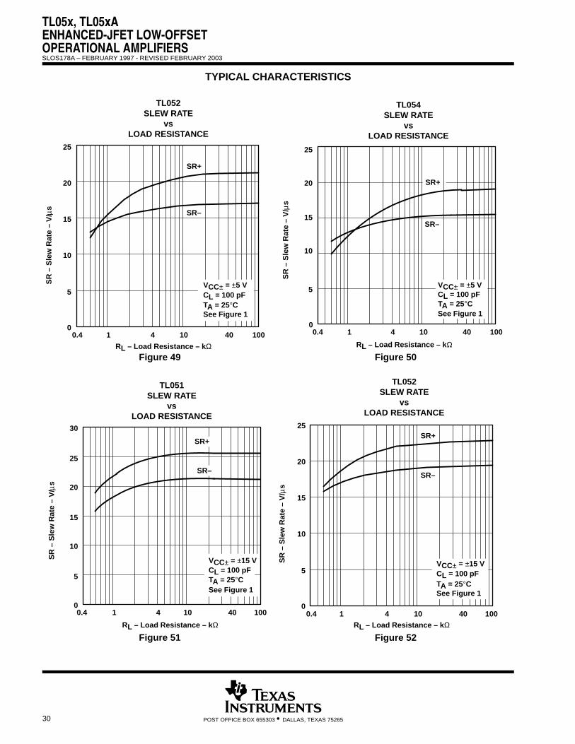
TYPICAL CHARACTERISTICS
10410.40
RL – Load Resistance – kΩ
25
5
10
15
20
SR–
SR+
40
CL = 100 pFTA = 25°CSee Figure 1
VCC± = ±5 VSR
– S
lew
Rat
e –
V/µ
s
Figure 49
TL052SLEW RATE
vsLOAD RESISTANCE
100
Figure 50
25
20
15
10
SR
– S
lew
Rat
e –
V/
5
0100401041
RL – Load Resistance – kΩ
0.4
ÎÎSR+
SR–
CL = 100 pFTA = 25°CSee Figure 1
VCC± = ±5 Vµ
s
TL054SLEW RATE
vsLOAD RESISTANCE
Figure 51
25
00.4
RL – Load Resistance – kΩ
5
10
15
20
30
1 4 10 40 100
SR+
SR–
SR
– S
lew
Rat
e –
V/µ
s
CL = 100 pFTA = 25°CSee Figure 1
VCC± = ±15 V
TL051SLEW RATE
vsLOAD RESISTANCE
1 4 10 40 1000.4RL – Load Resistance – kΩ
SR+
SR–
CL = 100 pFTA = 25°CSee Figure 1
VCC± = ±15 VSR
– S
lew
Rat
e –
V/µ
s
0
25
5
10
15
20
Figure 52
TL052SLEW RATE
vsLOAD RESISTANCE

TL05x, TL05xAENHANCED-JFET LOW-OFFSET
OPERATIONAL AMPLIFIERS
SLOS178A – FEBRUARY 1997 - REVISED FEBRUARY 2003
31POST OFFICE BOX 655303 • DALLAS, TEXAS 75265
TYPICAL CHARACTERISTICS
Figure 53
20
00.4
RL – Load Resistance – kΩ
5
10
15
25
1 4 10 40 100
SR+
SR–
SR
– S
lew
Rat
e –
V/µ
s
CL = 100 pFTA = 25°CSee Figure 1
VCC± = ±5 V
TL054SLEW RATE
vsLOAD RESISTANCE
Figure 54
–750
TA – Free-Air Temperature – °C125
30
–50 –25 0 25 50 75 100
5
10
15
20
25
VCC± = ±5 VRL = 2 kΩ
SR+
SR–
SR
– S
lew
Rat
e –
V/µ
s
TL051SLEW RATE†
vsFREE-AIR TEMPERATURE
Figure 55
SR+
SR–
–750
TA – Free-Air Temperature – °C125–50 –25 0 25 50 75 100
5
10
15
20
25
VCC± = ±5 VRL = 2 kΩCL = 100 pFSee Figure 1
SR
– S
lew
Rat
e –
V/µ
s
TL052SLEW RATE†
vsFREE-AIR TEMPERATURE
Figure 56
SR+
SR–
–750
TA – Free-Air Temperature – °C125–50 –25 0 25 50 75 100
5
10
15
20
VCC± = ±5 VRL = 2 kΩCL = 100 pFSee Figure 1
SR
– S
lew
Rat
e –
V/µ
s
TL054SLEW RATE†
vsFREE-AIR TEMPERATURE
† Data at high and low temperatures are applicable only within the rated operating free-air temperature ranges of the various devices.

TL05x, TL05xAENHANCED-JFET LOW-OFFSETOPERATIONAL AMPLIFIERS
SLOS178A – FEBRUARY 1997 - REVISED FEBRUARY 2003
32 POST OFFICE BOX 655303 • DALLAS, TEXAS 75265
TYPICAL CHARACTERISTICS
Figure 57
–750
TA – Free-Air Temperature – °C125
30
–50 –25 0 25 50 75 100
5
10
15
20
25
VCC± = ±15 VRL = 2 kΩCL = 100 pFSee Figure 1
SR–
SR+
SR
– S
lew
Rat
e –
V/µ
s
TL051SLEW RATE†
vsFREE-AIR TEMPERATURE
SR–
SR+
–750
TA – Free-Air Temperature – °C125–50 –25 0 25 50 75 100
5
10
15
20
25
VCC± = ±15 VRL = 2 kΩCL = 100 pFSee Figure 1
SR
– S
lew
Rat
e –
V/µ
s
Figure 58
TL052SLEW RATE†
vsFREE-AIR TEMPERATURE
Figure 59
SR–
SR+
–750
TA – Free-Air Temperature – °C125–50 –25 0 25 50 75 100
5
10
15
20
VCC± = ±15 VRL = 2 kΩCL = 100 pFSee Figure 1
SR
– S
lew
Rat
e –
V/µ
s
TL054SLEW RATE†
vsFREE-AIR TEMPERATURE
Figure 60
ÎÎÎÎÎÎÎÎÎÎ
See Figure 1ÎÎÎÎÎTA = 25°CÎÎÎÎÎRL = 2 kΩÎÎÎÎÎÎÎÎÎÎ
VI(PP) = ±10 mV
00
Ove
rsh
oo
t F
acto
r –
%
CL – Load Capacitance – pF
300
50
50 100 150 200 250
10
20
30
40
OVERSHOOT FACTORvs
LOAD CAPACITANCE
ÎÎÎÎÎVCC± = ±15 V
ÎÎÎÎÎÎÎÎVCC± = ±5 V
† Data at high and low temperatures are applicable only within the rated operating free-air temperature ranges of the various devices.

TL05x, TL05xAENHANCED-JFET LOW-OFFSET
OPERATIONAL AMPLIFIERS
SLOS178A – FEBRUARY 1997 - REVISED FEBRUARY 2003
33POST OFFICE BOX 655303 • DALLAS, TEXAS 75265
TYPICAL CHARACTERISTICS
Figure 61f – Frequency – Hz
10
Vn
– E
qu
ival
ent
Inp
ut
No
ise
Vo
ltag
e –
10
20
30
40
50
70
100
100 1 k 10 k 100 k
VCC± = ±15 VRS = 20 ΩTA = 25°CSee Figure 3
nV
/H
z
TL051EQUIVALENT INPUT NOISE VOLTAGE
vsFREQUENCY
f – Frequency – Hz
10
Vn
– E
qu
ival
ent
Inp
ut
No
ise
Vo
ltag
e –
10
20
30
40
50
70
100
100 1 k 10 k 100 k
nV
/H
z ÁÁÁÁÁÁÁÁÁÁÁÁÁÁÁÁÁÁÁÁ
VCC± = ±15 VRS = 20 ΩTA = 25°CSee Figure 3
Figure 62
TL052 AND TL054EQUIVALENT INPUT NOISE VOLTAGE
vsFREQUENCY
VO(RMS) = 6 V
0.001100
f – Frequency – Hz
TH
D –
To
tal H
arm
on
ic D
isto
rtio
n –
%
0.01
0.1
1
1 k 10 k 100 k
VCC± = ±15 VAVD = 1
TA = 25°C
TOTAL HARMONIC DISTORTIONvs
FREQUENCY
0.004
0.04
0.4
Figure 63 Figure 64
02.7
– U
nit
y-G
ain
Ban
dw
idth
– M
Hz
|VCC±| – Supply Voltage – V
16
3.2
2 4 6 8 10 12 14
2.8
2.9
3
3.1
VI = 10 mVRL = 2 kΩCL = 25 pFTA = 25°CSee Figure 4
B1
TL051UNITY-GAIN BANDWIDTH
vsSUPPLY VOLTAGE

TL05x, TL05xAENHANCED-JFET LOW-OFFSETOPERATIONAL AMPLIFIERS
SLOS178A – FEBRUARY 1997 - REVISED FEBRUARY 2003
34 POST OFFICE BOX 655303 • DALLAS, TEXAS 75265
TYPICAL CHARACTERISTICS
Figure 65
ÁÁÁÁÁÁÁÁÁÁÁÁÁÁÁÁÁÁÁÁ
VI = 10 mVRL = 2 kΩCL = 25 pF
See Figure 4TA = 25°C
2.7
– U
nit
y-G
ain
Ban
dw
idth
– M
Hz
|VCC±| – Supply Voltage – V
16
3.2
4 6 8 10 12 14
2.8
2.9
3
3.1
B1
TL052UNITY-GAIN BANDWIDTH
vsSUPPLY VOLTAGE
Figure 66
ÁÁÁÁÁÁÁÁÁÁÁÁÁÁÁÁÁÁÁÁÁÁÁÁÁ2.4
– U
nit
y-G
ain
Ban
dw
idth
– M
Hz
|VCC±| – Supply Voltage – V
16
2.9
0 2 6 8 10 14
2.5
2.6
2.7
2.8
B1
ÎÎÎÎÎÎÎÎ
VI = 10 mVÎÎÎÎÎÎÎÎÎÎ
RL = 2 kΩ
ÎÎÎÎÎÎCL = 25 pF
ÎÎÎÎÎÎÎÎÎÎÎÎÎÎ
See Figure 4
ÎÎÎÎÎÎÎÎÎÎ
TA = 25°C
4 12
TL054UNITY-GAIN BANDWIDTH
vsSUPPLY VOLTAGE
Figure 67
–750
TA – Free-Air Temperature – °C125
4
–50 –25 0 25 50 75 100
1
2
3
See Figure 4
VI = 10 mVRL = 2 kΩCL = 25 pF
VCC± = ±15 V
VCC± = ±5 V
– U
nit
y-G
ain
Ban
dw
idth
– M
Hz
B1
TL051UNITY-GAIN BANDWIDTH†
vsFREE-AIR TEMPERATURE
Figure 68
See Figure 4
VCC± = ±5 V to ±15 V
RL = 2 kΩCL = 25 pFTA = 25°C
VI = 10 mV
–750
TA – Free-Air Temperature – °C125
4
–50 –25 0 25 50 75 100
1
2
3
– U
nit
y-G
ain
Ban
dw
idth
– M
Hz
B1
TL052UNITY-GAIN BANDWIDTH†
vsFREE-AIR TEMPERATURE
† Data at high and low temperatures are applicable only within the rated operating free-air temperature ranges of the various devices.

TL05x, TL05xAENHANCED-JFET LOW-OFFSET
OPERATIONAL AMPLIFIERS
SLOS178A – FEBRUARY 1997 - REVISED FEBRUARY 2003
35POST OFFICE BOX 655303 • DALLAS, TEXAS 75265
TYPICAL CHARACTERISTICS
Figure 69
See Figure 4
VCC± = ±5 V to ±15 V
RL = 2 kΩCL = 25 pFTA = 25°C
VI = 10 mV
–750
TA – Free-Air Temperature – °C125
4
–50 –25 0 25 50 75 100
1
2
3
– U
nit
y-G
ain
Ban
dw
idth
– M
Hz
B1
TL054UNITY-GAIN BANDWIDTH†
vsFREE-AIR TEMPERATURE
Figure 70
055°
m
16
65°
2 4 6 8 10 12 14
57°
59°
61°
63°
|VCC±| – Supply Voltage – V
See Figure 4TA = 25°CCL = 25 pFRL = 2 kΩVI = 10 mVφ
– P
has
e M
arg
in
TL051PHASE MARGIN
vsSUPPLY VOLTAGE
Figure 71
55°
m
16
65°
4 6 8 10 12 14
57°
59°
61°
63°
|VCC±| – Supply Voltage – V
φ–
Ph
ase
Mar
gin
See Figure 4TA = 25°CCL = 25 pFRL = 2 kΩVI = 10 mV
TL052PHASE MARGIN
vsSUPPLY VOLTAGE
Figure 72
55°
m
16
65°
0 4 8 10 12 14
57°
59°
61°
63°
|VCC±| – Supply Voltage – V
φ–
Ph
ase
Mar
gin
62
ÁÁÁÁÁÁÁÁÁÁÁÁÁÁÁÁÁÁÁÁÁÁÁÁÁ
See Figure 4TA = 25°CCL = 25 pFRL = 2 kΩVI = 10 mV
TL054PHASE MARGIN
vsSUPPLY VOLTAGE
† Data at high and low temperatures are applicable only within the rated operating free-air temperature ranges of the various devices.

TL05x, TL05xAENHANCED-JFET LOW-OFFSETOPERATIONAL AMPLIFIERS
SLOS178A – FEBRUARY 1997 - REVISED FEBRUARY 2003
36 POST OFFICE BOX 655303 • DALLAS, TEXAS 75265
TYPICAL CHARACTERISTICS
Figure 73
040°
CL – Load Capacitance – pF100
70°
10 20 30 40 50 60 70 80 90
45°
50°
55°
60°
65°
VI = 10 mVRL = 2 kΩTA = 25°CSee Figure 4
VCC± = ±15 VSee Note A
VCC± = ±5 V
mφ
– P
has
e M
arg
in
TL051PHASE MARGIN†
vsLOAD CAPACITANCE
Figure 74
0CL – Load Capacitance – pF
70°
10 20 30 40 50 60 70 80 9045°
50°
55°
60°
65°
VI = 10 mVRL = 2 kΩTA = 25°CSee Figure 4
ÎÎÎÎÎVCC± = ±15 V
See Note A
ÎÎÎÎÎÎÎÎÎÎ
VCC± = ±5 V
mφ
– P
has
e M
arg
in
TL052PHASE MARGIN†
vsLOAD CAPACITANCE
100
0CL – Load Capacitance – pF
100
70°
10 20 30 40 50 60 70 80 9045°
50°
55°
60°
65°
VI = 10 mVRL = 2 kΩTA = 25°CSee Figure 4
ÎÎÎÎÎÎÎÎÎÎVCC± = ±15 V
See Note A
ÎÎÎÎÎVCC± = ±5 V
mφ–
Ph
ase
Mar
gin
TL054PHASE MARGIN†
vsLOAD CAPACITANCE
Figure 75
† Values of phase margin below a load capacitance of 25 pF were estimated.

TL05x, TL05xAENHANCED-JFET LOW-OFFSET
OPERATIONAL AMPLIFIERS
SLOS178A – FEBRUARY 1997 - REVISED FEBRUARY 2003
37POST OFFICE BOX 655303 • DALLAS, TEXAS 75265
TYPICAL CHARACTERISTICS
Figure 76
–7555°
TA – Free-Air Temperature – °C125
65°
–50 –25 0 25 50 75 100
57°
59°
61°
63°VCC± = ±15 V
VCC± = ±5 V
ÁÁÁÁÁÁÁÁÁÁÁÁÁÁÁÁÁÁÁÁ
CL = 25 pF
VI = 10 mVRL = 2 kΩ
See Figure 4
mφ
– P
has
e M
arg
in
TL051PHASE MARGIN†
vsFREE-AIR TEMPERATURE
Figure 77
–7555°
TA – Free-Air Temperature – °C125
65°
–50 –25 0 25 50 75 100
57°
59°
61°
63°VCC± = ±15 V
VCC± = ±5 V
ÁÁÁÁÁÁÁÁÁÁÁÁÁÁÁÁÁÁÁÁ
CL = 25 pF
VI = 10 mVRL = 2 kΩ
See Figure 4
mφ
– P
has
e M
arg
in
TL052PHASE MARGIN†
vsFREE-AIR TEMPERATURE
–7555°
TA – Free-Air Temperature – °C125
65°
–50 –25 0 25 50 75 100
57°
59°
61°
63°VCC± = ±15 V
VCC± = ±5 V
ÁÁÁÁÁÁÁÁÁÁÁÁÁÁÁÁÁÁÁÁ
CL = 25 pF
VI = 10 mVRL = 2 kΩ
See Figure 4
mφ–
Ph
ase
Mar
gin
TL054PHASE MARGIN†
vsFREE-AIR TEMPERATURE
Figure 78
† Data at high and low temperatures are applicable only within the rated operating free-air temperature ranges of the various devices.

TL05x, TL05xAENHANCED-JFET LOW-OFFSETOPERATIONAL AMPLIFIERS
SLOS178A – FEBRUARY 1997 - REVISED FEBRUARY 2003
38 POST OFFICE BOX 655303 • DALLAS, TEXAS 75265
TYPICAL CHARACTERISTICS
–16
– O
utp
ut
Vo
ltag
e –
mV
t – Time – µs
1.2
16
0 0.2 0.4 0.6 0.8 1.0
–12
–8
–4
0
4
8
12
VOLTAGE-FOLLOWERSMALL-SIGNAL
PULSE RESPONSE
VO
ÁÁÁÁÁÁÁÁÁÁÁÁÁÁÁÁÁÁÁÁ
VCC± = ±15 VRL = 2 kΩCL = 100 pFTA = 25°CSee Figure 1
Figure 79
–8
t – Time – µs
6
8
0 1 2 3 4 5
–6
–4
–2
0
2
4
6
VOLTAGE-FOLLOWERLARGE-SIGNAL
PULSE RESPONSE
– O
utp
ut
Vo
ltag
e –
VV
O
ÁÁÁÁÁÁÁÁÁÁÁÁÁÁÁÁÁÁÁÁÁÁÁÁÁ
VCC± = ±15 VRL = 2 kΩCL = 100 pFTA = 25°CSee Figure 1
Figure 80

TL05x, TL05xAENHANCED-JFET LOW-OFFSET
OPERATIONAL AMPLIFIERS
SLOS178A – FEBRUARY 1997 - REVISED FEBRUARY 2003
39POST OFFICE BOX 655303 • DALLAS, TEXAS 75265
APPLICATION INFORMATION
output characteristics
All operating characteristics (except bandwidth and phase margin) are specified with 100-pF load capacitance.The TL05x and TL05xA drive higher capacitive loads; however, as the load capacitance increases, the resultingresponse pole occurs at lower frequencies, causing ringing, peaking, or even oscillation. The value of the loadcapacitance at which oscillation occurs varies with production lots. If an application appears to be sensitive tooscillation due to load capacitance, adding a small resistance in series with the load should alleviate theproblem. Capacitive loads of 1000 pF, and larger, may be driven if enough resistance is added in series withthe output (see Figure 81 and Figure 82).
(a) CL = 100 pF, R = 0 (b) CL = 300 pF, R = 0 (c) CL = 350 pF, R = 0
(d) CL = 1000 pF, R = 0 (e) CL = 1000 pF, R = 50 Ω (f) CL = 1000 pF, R = 2 kΩ
Figure 81. Effect of Capacitive Loads
+
–
5 V
–5 V
15 V
–15 V
CL(see Note A)
2 kΩ
VOR
NOTE A: CL includes fixture capacitance.
Figure 82. Test Circuit for Output Characteristics

TL05x, TL05xAENHANCED-JFET LOW-OFFSETOPERATIONAL AMPLIFIERS
SLOS178A – FEBRUARY 1997 - REVISED FEBRUARY 2003
40 POST OFFICE BOX 655303 • DALLAS, TEXAS 75265
APPLICATION INFORMATION
input characteristics
The TL05x and TL05xA are specified with a minimum and a maximum input voltage that, if exceeded at eitherinput, could cause the device to malfunction.
Because of the extremely high input impedance and resulting low-bias current requirements, the TL05x andTL05xA are well suited for low-level signal processing; however, leakage currents on printed-circuit boards andsockets easily can exceed bias current requirements and cause degradation in system performance. It is goodpractice to include guard rings around inputs (see Figure 83). These guards should be driven from alow-impedance source at the same voltage level as the common-mode input.
Unused amplifiers should be connected as grounded unity-gain followers to avoid possible oscillation.
+
–
+
–
+
–
VO
VO VO
VI
VI
(a) NONINVERTING AMPLIFIER (b) INVERTING AMPLIFIER (c) UNITY-GAIN AMPLIFIER
VI
Figure 83. Use of Guard Rings
noise performance
The noise specifications in operational amplifier circuits are greatly dependent on the current in the first-stagedifferential amplifier. The low input-bias current requirements of the TL05x and TL05xA result in a very lowcurrent noise. This feature makes the devices especially favorable over bipolar devices when using values ofcircuit impedance greater than 50 kΩ.

TL05x, TL05xAENHANCED-JFET LOW-OFFSET
OPERATIONAL AMPLIFIERS
SLOS178A – FEBRUARY 1997 - REVISED FEBRUARY 2003
41POST OFFICE BOX 655303 • DALLAS, TEXAS 75265
APPLICATION INFORMATION
phase meter
The phase meter in Figure 84 produces an output voltage of 10 mV per degree of phase delay between the twoinput signals VA and VB. The reference signal VA must be the same frequency as VB. The TLC3702 comparators(U1) convert these two input sine waves into ±5-V square waves. Then, R1 and R4 provide level shifting priorto the SN74HC109 dual J-K flip flops.
Flip-flop U2B is connected as a toggle flip-flop and generates a square wave at one-half the frequency of VB.Flip-flop U2A also produces a square wave at one-half the input frequency. The pulse duration of U2A variesfrom zero to one-half the period, where zero corresponds to zero phase delay between VA and VB and one-halfthe period corresponds to VB lagging VA by 360 degrees.
The output pulse from U2A causes the TLC4066 (U3) switch to charge the TL05x (U4) integrator capacitors C1and C2. As the phase delay approaches 360 degrees, the output of U4A approximates a square wave, and U2Ahas an output of almost 2.5 V. U4B acts as a noninverting amplifier with a gain of 1.44 in order to scale the0- to 2.5-V integrator output to a 0- to 3.6-V output range.
R8 and R10 provide output gain and zero-level calibration. This circuit operates over a 100-Hz to 10-kHzfrequency range.
+
–+
–
+5 V
R2100 kΩ
R1
100 kΩU1A
VAS
1JC1
U2A
1KR
NC
U2B
2K
R3
VBU1B
R6
10 kΩ
R7
10 kΩ
+5 V
S2J
C1
R
NC100 kΩ
R4100 kΩ
U3
R5 C110 kΩ 0.016 µF
C20.016 µF
U4AU4B VO
R9
20 kΩ
R8
Gain50 kΩ
+5 V
R1010 kΩZero
–5 V
NOTE A: U1 = TLC3702; VCC± = ±5 VU2 = SN74HC109U3 = TLC4066U4, U5 = TL05x; VCC± = ±5 V
Figure 84. Phase Meter

TL05x, TL05xAENHANCED-JFET LOW-OFFSETOPERATIONAL AMPLIFIERS
SLOS178A – FEBRUARY 1997 - REVISED FEBRUARY 2003
42 POST OFFICE BOX 655303 • DALLAS, TEXAS 75265
APPLICATION INFORMATION
precision constant-current source over temperature
A precision current source (see Figure 85) benefits from the high input impedance and stability of TexasInstruments enhanced-JFET process. A low-current shunt regulator maintains 2.5 V between the inverting inputand the output of the TL05x. The negative feedback then forces 2.5 V across the current-setting resistor R;therefore, the current to the load simply is 2.5 V divided by R.
Possible choices for the shunt regulator include the LT1004, LT1009, and LM385. If the regulator’s cathodeconnects to the operational amplifier output, this circuit sources load current. Similarly, if the cathode connectsto the inverting input, the circuit sinks current from the load. To minimize output current change with temperature,R should be a metal film resistor with a low temperature coefficient. Also, this circuit must be operated withsplit-voltage supplies.
+
–
+
–
150 pF
U2
+15 V
U1
–15 V
R
100 kΩ
IO
LoadV = 0 to 10 V
(a) SOURCE CURRENT LOAD (b) SINK CURRENT LOAD
V = 0 to –10 VLoad
II
R
–15 V
U1
+15 V
150 pF
U2
100 kΩ
NOTE A: U1 = 1/2 TL05x U2 = LM385, LT1004, or LT1009 voltage reference
I = 2.5 VR
, R = Low-temperature-coefficient metal-film resistor
Figure 85. Precision Constant-Current Source

TL05x, TL05xAENHANCED-JFET LOW-OFFSET
OPERATIONAL AMPLIFIERS
SLOS178A – FEBRUARY 1997 - REVISED FEBRUARY 2003
43POST OFFICE BOX 655303 • DALLAS, TEXAS 75265
APPLICATION INFORMATION
instrumentation amplifier with adjustable gain/null
The instrumentation amplifier in Figure 86 benefits greatly from the high input impedance and stable input offsetvoltage of the TL05xA. Amplifiers U1A, U1B, and U2A form the actual instrumentation amplifier, while U2Bprovides offset null. Potentiometer R1 provides gain adjustment. With R1 = 2 kΩ, the circuit gain equals 100,while with R1 = 200 kΩ, the circuit gain equals two. The following equation shows the instrumentation amplifiergain as a function of R1:
AV 1 R2 R3R1
Readjusting the offset null is necessary when the circuit gain is changed. If U2B is needed for anotherapplication, R7 can be terminated at ground. The low input offset voltage of the TL05xA minimizes the dc errorof the circuit. For best matching, all resistors should be one-percent tolerance. The matching between R4, R5,R6, and R7 controls the CMRR of this application.
The following equation shows the output voltages when the input voltage equals zero. This dc error can benulled by adjusting the offset null potentiometer; however, any change in offset voltage over time or temperaturealso creates an error. To calculate the error from changes in offset, consider the three offset components in theequation as delta offsets, rather than initial offsets. The improved stability of Texas Instruments enhanced JFETsminimizes the error resulting from change in input offset voltage with time. Assuming VI equals zero, VO canbe shown as a function of the offset voltage:
–VIO1R3R1
R7R5 R7
1 R6R4 R6
R41 R2
R1 VIO3
1 R6R4
VO VIO21 R3
R1 R7
R5 R7 1 R6
R4 R2
R1R6R4
NOTE A: U1 and U2 = TL05xA; VCC± = ±15 V.
100 kΩ
U2A
+
–
+
–
+
–
+
–
VI–U1A
R4
10 kΩ
R6
10 kΩ
200 kΩ
R2
10 MΩ
100 kΩ
10 turn
AV = 2 to 1002 kΩ R1
U1B
VI+
R5 R7U2B
0.1 µF
Offset Null
VCC–
82 kΩ
82 kΩ
VCC+R3
VO
10 kΩ 10 kΩ
10 MΩ
1 kΩ
Figure 86. Instrumentation Amplifier

TL05x, TL05xAENHANCED-JFET LOW-OFFSETOPERATIONAL AMPLIFIERS
SLOS178A – FEBRUARY 1997 - REVISED FEBRUARY 2003
44 POST OFFICE BOX 655303 • DALLAS, TEXAS 75265
APPLICATION INFORMATION
high input impedance log amplifier
The low input offset voltage and high input impedance of the TL05xA creates a precision log amplifier (seeFigure 87). IC1 is a 2.5-V, low-current precision, shunt regulator. Transistors Q1 and Q2 must be a closelymatched npn pair. For best performance over temperature, R4 should be a metal-film resistor with a lowtemperature coefficient.
In this circuit, U1A serves as a high-impedance unity-gain buffer. Amplifier U1B converts the input voltage toa current through R1 and Q1. Amplifier U1C, IC1, and R4 form a 1-µA temperature-stable current source thatsets the base-emitter voltage of Q2. U1D amplifies the difference between the base-emitter voltage of Q1 andQ2 (see Figure 88). The output voltage is given by the following equation:
VO –1 R6R5 kT
q
InVI
R1 1 10–6
where k 1.38 10–23, q 1.602 10–19,and T is Kelvin temperature
_+ _
+
U1A_+U1B
_+U1C U1D
VI
R1
10 kΩ
Q1 Q2
2N2484
R215 V 10 kΩ
2.5 MΩ
R4
150 pF
C1
IC1270 kΩ
R3
–15V
R510 kΩ
R6
10 kΩ
VO(see equation above)
NOTE A: U1A through U1D = TL05xA. IC1 = LM385, LT1004, or LT1009 voltage reference
Figure 87. Log Amplifier
0 1 2 3 4 5 6
– D
iffe
ren
tial
Vo
ltag
e A
mp
lific
atio
n –
dB
f – Frequency – Hz
7 8 9 10–0.4
–0.35
–0.3
–0.25
–0.2
–0.15
–0.1
ÁÁÁÁÁÁ
AV
D
Figure 88. Output Voltage vs Input Voltage for Log Amplifier

TL05x, TL05xAENHANCED-JFET LOW-OFFSET
OPERATIONAL AMPLIFIERS
SLOS178A – FEBRUARY 1997 - REVISED FEBRUARY 2003
45POST OFFICE BOX 655303 • DALLAS, TEXAS 75265
APPLICATION INFORMATION
analog thermometer
By combining a current source that does not vary over temperature with an instrumentation amplifier, a preciseanalog thermometer can be built (see Figure 89). Amplifier U1A and IC1 establish a constant current throughthe temperature-sensing diode D1. For this section of the circuit to operate correctly, the TL05x must use splitsupplies, and R3 must be a metal-film resistor with a low temperature coefficient.
The temperature-sensitive voltage from the diode is compared to a temperature-stable voltage reference setby IC2. R4 should be adjusted to provide the correct output voltage when the diode is at a known temperature.Although this potentiometer resistance varies with temperature, the divider ratio of the potentiometer remainsconstant.
Amplifiers U1B, U2A, and U2B form the instrumentation amplifier that converts the difference between the diodeand reference voltage to a voltage proportional to the temperature. With switch S1 closed, the amplifier gainequals 5 and the output voltage is proportional to temperature in degrees Celsius. With S1 open, the amplifiergain is 9 and the output is proportional to temperature in degrees Fahrenheit. Every time S1 is changed, R4 mustbe recalibrated. By setting S1 correctly, the output voltage equals 10 mV per degree (C or F).
+
–
+
–
+
–
IC1
C1
150 pFR1
100 kΩ U1A
R3 10 kΩ(see Note B)
D1(see Note A) +15 V
R2 100 kΩ
IC2R450 kΩ
U1B
R6
10 kΩ
R55 kΩ
R75 kΩ
S1(see Note C)
R8
10 kΩ
U2AR10
10 kΩR11
R9 R12
10 kΩ 10 kΩ
+15 V+
–
–15 V
10 kΩ
VO(see Note D)
U2B
NOTES: A. Temperature-sensing diode ≈ (–2 mV/°C)B. Metal-film resistor (low temperature coefficient)C. Switch open for °F and closed for °CD. VO α temperature; 10 mV/°C or 10 mV/°FE. U1, U2 = TL05x. IC1, IC2 = LM385, LT1004, or LT1009 voltage reference
Figure 89. Analog Thermometer

TL05x, TL05xAENHANCED-JFET LOW-OFFSETOPERATIONAL AMPLIFIERS
SLOS178A – FEBRUARY 1997 - REVISED FEBRUARY 2003
46 POST OFFICE BOX 655303 • DALLAS, TEXAS 75265
APPLICATION INFORMATION
voltage-ratio-to-dB converter
The application in Figure 90 measures the amplitude ratio of two signals, then converts the ratio to decibels (seeFigure 91). The output voltage provides a resolution of 100 mV/dB. The two inputs can be either dc or sinusoidalac signals. When using ac signals, both signals should be the same frequency or output glitches will occur. Formeasuring two input signals of different frequencies, extra filtering should be added after the rectifiers.
The circuit contains three low-offset TL05xA devices. Two of these devices provide the rectification andlogarithmic conversion of the inputs. The third TL05xA forms an instrumentation amplifier. The stage performingthe logarithmic conversion also requires two well-matched npn transistors.
The input signal first passes through a high-impedance unity-gain buffer U1A (U2A). Then U1B (U2B) rectifiesthe input signal at a gain of 0.5, and U1C (U2C) provides a noninverting gain of 2, so that the system gain isstill one. U1D (U2D), R6 (R13), and Q1 (Q2) perform the logarithmic conversion of the rectified input signal. Theinstrumentation amplifier formed by U3A, U3B, U3D scales the difference of the two logarithmic voltages by again of 33.6. As a result, the output voltage equals 100 mV/dB. The 1-kΩ potentiometer on the input of U3Ccalibrates the zero-dB reference level. The following equations are used to derive the relationship between theinput voltage ratio, expressed in decibels, and the output voltage.
X dB 20 logVAVB 20
In VA – VB
In (10)
X dB 8.686 In VA – In VB
VBE(Q1) kTq In VA
R IS VBE(Q2)
kTq In VB
R IS
VBE VBE(Q1) –VBE(Q2) kTq In VA
– In VB
X dB 8.686kTq
VBE(Q1) –VBE(Q2) 336 VBE(Q1) –VBE(Q2)
at 25°C
where
k 1.38 10–23, q 1.602 10–19, and T is Kelvin temperature
This gives a resolution of 1 V/dB. Therefore, the gain of the instrumentation amplifier is set at 33.6 to obtain100 mV/dB.

TL05x, TL05xAENHANCED-JFET LOW-OFFSET
OPERATIONAL AMPLIFIERS
SLOS178A – FEBRUARY 1997 - REVISED FEBRUARY 2003
47POST OFFICE BOX 655303 • DALLAS, TEXAS 75265
APPLICATION INFORMATION
_+
_+
_+
_+
_+
_+
_+
_+
_+_
+_+
_+
U1A
U3A
U3B
U3C
U3D
U1BU1C
U1D
U2AU2B
U2CU2D
VA
VB
VO
R1
20 kΩ
R8
20 kΩ
R2
10 kΩ
R9
10 kΩ
D1
D2
R330 kΩ
R1030 kΩ
R410 kΩ
R5
10 kΩ
R6
10 kΩR7
10 kΩ
2N2484 Q1
Q2
R16
16.3 kΩ
R18
10 kΩ
R20
10 kΩ
R1110 kΩ
R12
10 kΩ
R13
10 kΩ
2N2484
R14
10 kΩ
R76
16.3 kΩR19
10 kΩR2110 kΩ
C1
15 V
–15 V
82 kΩ
1 kΩ
82 kΩ
NOTE A: U1A through U3D = TL05xA, VCC± = ±15 V. D1 and D2 = 1N914.
Figure 90. Voltage Ratio-to-dB Converter
0 1 2 3 4 5 6
– O
utp
ut
Vo
ltag
e –
V
7 8 9 10–2
–1
0
1
2
Ratio – VA/VB
VO
Figure 91. Output Voltage vs the Ratio of the Input Voltages for Voltage-to-dB Converter

TL05x, TL05xAENHANCED-JFET LOW-OFFSETOPERATIONAL AMPLIFIERS
SLOS178A – FEBRUARY 1997 - REVISED FEBRUARY 2003
48 POST OFFICE BOX 655303 • DALLAS, TEXAS 75265
APPLICATION INFORMATION
macromodel information
Macromodel information provided was derived using Microsim Parts , the model-generation software usedwith Microsim PSpice . The Boyle macromodel (see Note 6 and subcircuit Figure 92) are generated using theTL05x typical electrical and operating characteristics at TA = 25°C. Using this information, output simulationsof the following key parameters can be generated to a tolerance of 20% (in most cases):
Maximum positive output voltage swing Maximum negative output voltage swing Slew rate Quiescent power dissipation Input bias current Open-loop voltage amplification
Unity-gain frequency Common-mode rejection ratio Phase margin DC output resistance AC output resistance Short-circuit output current limit
NOTE 6: G. R. Boyle, B. M. Cohn, D. O. Pederson, and J. E. Solomon, “Macromodeling of Integrated Circuit Operational Amplifiers”, IEEE Journalof Solid-State Circuits, SC-9, 353 (1974).
OUT
+
–
+
–
+
–
+
–
+–
+
–
+
– +
–
+–
.SUBCKT TL05x 1 2 3 4 5C1 11 12 3.988E–12C2 6 7 15.00E–12DC 5 53 DXDE 54 5 DXDLP 90 91 DXDLN 92 90 DXDP 4 3 DXEGND99 0 POLY (2) (3,0) (4,0) 0 .5 .5FB 7 99 POLY (5) VB VC VE VLP+ VLN 0 2.875E6 –3E6 3E6 3E6 –3E6GA 6 0 11 12 292.2E–6GCM 0 6 10 99 6.542E–9ISS 3 10 DC 300.0E–6HLIM 90 0 VLIM 1KJ1 11 2 10 JXJ2 12 1 10 JXR2 6 9 100.0E3
RD1 4 11 3.422E3RD2 4 12 3.422E3R01 8 5 125R02 7 99 125RP 3 4 11.11E3RSS 10 99 666.7E6VB 9 0 DC 0VC 3 53 DC 3VE 54 4 DC 3.7VLIM 7 8 DC 0VLP 91 0 DC 28VLN 0 92 DC 28.MODEL DX D (IS=800.0E–18).MODEL JX PJF (IS=15.00E–12 BETA=185.2E–6+ VTO=–.1).ENDS
VCC+
RP
IN–2
IN+3
VCC–VAD
RD1
11
J1 J2
10
RSS ISS
3
12
RD2
60
VE
54DE
DP
VC
DC
4
C1
53
R2
6
9
EGND
VB
FB
C2
GCM GA VLIM
8
5
RO1
RO2
HLIM
90
DLP
91
DLN
92
VLNVLP
99
7
Figure 92. Boyle Macromodel and Subcircuit
PSpice and Parts are trademarks of MicroSim Corporation.
Macromodels, simulation models, or other models provided by TI,directly or indirectly, are not warranted by TI as fully representing allof the specification and operating characteristics of thesemiconductor product to which the model relates.

PACKAGE OPTION ADDENDUM
www.ti.com 2-Jun-2017
Addendum-Page 1
PACKAGING INFORMATION
Orderable Device Status(1)
Package Type PackageDrawing
Pins PackageQty
Eco Plan(2)
Lead/Ball Finish(6)
MSL Peak Temp(3)
Op Temp (°C) Device Marking(4/5)
Samples
TL051ACD ACTIVE SOIC D 8 75 Green (RoHS& no Sb/Br)
CU NIPDAU Level-1-260C-UNLIM 0 to 70 051AC
TL051ACDG4 ACTIVE SOIC D 8 75 Green (RoHS& no Sb/Br)
CU NIPDAU Level-1-260C-UNLIM 0 to 70 051AC
TL051ACP ACTIVE PDIP P 8 50 Pb-Free(RoHS)
CU NIPDAU N / A for Pkg Type 0 to 70 TL051ACP
TL051CD ACTIVE SOIC D 8 75 Green (RoHS& no Sb/Br)
CU NIPDAU Level-1-260C-UNLIM 0 to 70 TL051C
TL051CDR ACTIVE SOIC D 8 2500 Green (RoHS& no Sb/Br)
CU NIPDAU Level-1-260C-UNLIM 0 to 70 TL051C
TL051CDRG4 ACTIVE SOIC D 8 2500 Green (RoHS& no Sb/Br)
CU NIPDAU Level-1-260C-UNLIM 0 to 70 TL051C
TL051CP ACTIVE PDIP P 8 50 Pb-Free(RoHS)
CU NIPDAU N / A for Pkg Type 0 to 70 TL051CP
TL051CPE4 ACTIVE PDIP P 8 50 Pb-Free(RoHS)
CU NIPDAU N / A for Pkg Type 0 to 70 TL051CP
TL052ACD ACTIVE SOIC D 8 75 Green (RoHS& no Sb/Br)
CU NIPDAU Level-1-260C-UNLIM 0 to 70 052AC
TL052ACDG4 ACTIVE SOIC D 8 75 Green (RoHS& no Sb/Br)
CU NIPDAU Level-1-260C-UNLIM 0 to 70 052AC
TL052ACDR ACTIVE SOIC D 8 2500 Green (RoHS& no Sb/Br)
CU NIPDAU Level-1-260C-UNLIM 0 to 70 052AC
TL052ACDRG4 ACTIVE SOIC D 8 2500 Green (RoHS& no Sb/Br)
CU NIPDAU Level-1-260C-UNLIM 0 to 70 052AC
TL052ACP ACTIVE PDIP P 8 50 Pb-Free(RoHS)
CU NIPDAU N / A for Pkg Type 0 to 70 TL052ACP
TL052ACPE4 ACTIVE PDIP P 8 50 Pb-Free(RoHS)
CU NIPDAU N / A for Pkg Type 0 to 70 TL052ACP
TL052AID ACTIVE SOIC D 8 75 Green (RoHS& no Sb/Br)
CU NIPDAU Level-1-260C-UNLIM -40 to 85 052AI
TL052AIDE4 ACTIVE SOIC D 8 75 Green (RoHS& no Sb/Br)
CU NIPDAU Level-1-260C-UNLIM -40 to 85 052AI
TL052AIDG4 ACTIVE SOIC D 8 75 Green (RoHS& no Sb/Br)
CU NIPDAU Level-1-260C-UNLIM -40 to 85 052AI

PACKAGE OPTION ADDENDUM
www.ti.com 2-Jun-2017
Addendum-Page 2
Orderable Device Status(1)
Package Type PackageDrawing
Pins PackageQty
Eco Plan(2)
Lead/Ball Finish(6)
MSL Peak Temp(3)
Op Temp (°C) Device Marking(4/5)
Samples
TL052AIDR ACTIVE SOIC D 8 2500 Green (RoHS& no Sb/Br)
CU NIPDAU Level-1-260C-UNLIM -40 to 85 052AI
TL052AIDRG4 ACTIVE SOIC D 8 2500 Green (RoHS& no Sb/Br)
CU NIPDAU Level-1-260C-UNLIM -40 to 85 052AI
TL052AIP ACTIVE PDIP P 8 50 Pb-Free(RoHS)
CU NIPDAU N / A for Pkg Type -40 to 85 TL052AIP
TL052CD ACTIVE SOIC D 8 75 Green (RoHS& no Sb/Br)
CU NIPDAU Level-1-260C-UNLIM 0 to 70 TL052C
TL052CDG4 ACTIVE SOIC D 8 75 Green (RoHS& no Sb/Br)
CU NIPDAU Level-1-260C-UNLIM 0 to 70 TL052C
TL052CDR ACTIVE SOIC D 8 2500 Green (RoHS& no Sb/Br)
CU NIPDAU Level-1-260C-UNLIM 0 to 70 TL052C
TL052CDRE4 ACTIVE SOIC D 8 2500 Green (RoHS& no Sb/Br)
CU NIPDAU Level-1-260C-UNLIM 0 to 70 TL052C
TL052CDRG4 ACTIVE SOIC D 8 2500 Green (RoHS& no Sb/Br)
CU NIPDAU Level-1-260C-UNLIM 0 to 70 TL052C
TL052CP ACTIVE PDIP P 8 50 Pb-Free(RoHS)
CU NIPDAU N / A for Pkg Type 0 to 70 TL052CP
TL052CPSR ACTIVE SO PS 8 2000 Green (RoHS& no Sb/Br)
CU NIPDAU Level-1-260C-UNLIM 0 to 70 T052
TL052ID ACTIVE SOIC D 8 75 Green (RoHS& no Sb/Br)
CU NIPDAU Level-1-260C-UNLIM -40 to 85 TL052I
TL052IDG4 ACTIVE SOIC D 8 75 Green (RoHS& no Sb/Br)
CU NIPDAU Level-1-260C-UNLIM -40 to 85 TL052I
TL052IDR ACTIVE SOIC D 8 2500 Green (RoHS& no Sb/Br)
CU NIPDAU Level-1-260C-UNLIM -40 to 85 TL052I
TL052IDRE4 ACTIVE SOIC D 8 2500 Green (RoHS& no Sb/Br)
CU NIPDAU Level-1-260C-UNLIM -40 to 85 TL052I
TL052IP ACTIVE PDIP P 8 50 Pb-Free(RoHS)
CU NIPDAU N / A for Pkg Type -40 to 85 TL052IP
TL052IPE4 ACTIVE PDIP P 8 50 Pb-Free(RoHS)
CU NIPDAU N / A for Pkg Type -40 to 85 TL052IP
TL054ACD ACTIVE SOIC D 14 50 Green (RoHS& no Sb/Br)
CU NIPDAU Level-1-260C-UNLIM 0 to 70 TL054AC
TL054ACDE4 ACTIVE SOIC D 14 50 Green (RoHS& no Sb/Br)
CU NIPDAU Level-1-260C-UNLIM 0 to 70 TL054AC

PACKAGE OPTION ADDENDUM
www.ti.com 2-Jun-2017
Addendum-Page 3
Orderable Device Status(1)
Package Type PackageDrawing
Pins PackageQty
Eco Plan(2)
Lead/Ball Finish(6)
MSL Peak Temp(3)
Op Temp (°C) Device Marking(4/5)
Samples
TL054ACDG4 ACTIVE SOIC D 14 50 Green (RoHS& no Sb/Br)
CU NIPDAU Level-1-260C-UNLIM 0 to 70 TL054AC
TL054ACDR ACTIVE SOIC D 14 2500 Green (RoHS& no Sb/Br)
CU NIPDAU Level-1-260C-UNLIM 0 to 70 TL054AC
TL054ACN ACTIVE PDIP N 14 25 Pb-Free(RoHS)
CU NIPDAU N / A for Pkg Type 0 to 70 TL054ACN
TL054AID ACTIVE SOIC D 14 50 Green (RoHS& no Sb/Br)
CU NIPDAU Level-1-260C-UNLIM -40 to 85 TL054AI
TL054AIDG4 ACTIVE SOIC D 14 50 Green (RoHS& no Sb/Br)
CU NIPDAU Level-1-260C-UNLIM -40 to 85 TL054AI
TL054AIDR ACTIVE SOIC D 14 2500 Green (RoHS& no Sb/Br)
CU NIPDAU Level-1-260C-UNLIM -40 to 85 TL054AI
TL054AIDRE4 ACTIVE SOIC D 14 2500 Green (RoHS& no Sb/Br)
CU NIPDAU Level-1-260C-UNLIM -40 to 85 TL054AI
TL054CD ACTIVE SOIC D 14 50 Green (RoHS& no Sb/Br)
CU NIPDAU Level-1-260C-UNLIM 0 to 70 TL054C
TL054CDE4 ACTIVE SOIC D 14 50 Green (RoHS& no Sb/Br)
CU NIPDAU Level-1-260C-UNLIM 0 to 70 TL054C
TL054CDR ACTIVE SOIC D 14 2500 Green (RoHS& no Sb/Br)
CU NIPDAU Level-1-260C-UNLIM 0 to 70 TL054C
TL054CDRG4 ACTIVE SOIC D 14 2500 Green (RoHS& no Sb/Br)
CU NIPDAU Level-1-260C-UNLIM 0 to 70 TL054C
TL054CN ACTIVE PDIP N 14 25 Pb-Free(RoHS)
CU NIPDAU N / A for Pkg Type 0 to 70 TL054CN
TL054CNE4 ACTIVE PDIP N 14 25 Pb-Free(RoHS)
CU NIPDAU N / A for Pkg Type 0 to 70 TL054CN
TL054CNSR ACTIVE SO NS 14 2000 Green (RoHS& no Sb/Br)
CU NIPDAU Level-1-260C-UNLIM 0 to 70 TL054
TL054ID ACTIVE SOIC D 14 50 Green (RoHS& no Sb/Br)
CU NIPDAU Level-1-260C-UNLIM -40 to 85 TL054I
TL054IDE4 ACTIVE SOIC D 14 50 Green (RoHS& no Sb/Br)
CU NIPDAU Level-1-260C-UNLIM -40 to 85 TL054I
TL054IDG4 ACTIVE SOIC D 14 50 Green (RoHS& no Sb/Br)
CU NIPDAU Level-1-260C-UNLIM -40 to 85 TL054I
TL054IDR ACTIVE SOIC D 14 2500 Green (RoHS& no Sb/Br)
CU NIPDAU Level-1-260C-UNLIM -40 to 85 TL054I

PACKAGE OPTION ADDENDUM
www.ti.com 2-Jun-2017
Addendum-Page 4
Orderable Device Status(1)
Package Type PackageDrawing
Pins PackageQty
Eco Plan(2)
Lead/Ball Finish(6)
MSL Peak Temp(3)
Op Temp (°C) Device Marking(4/5)
Samples
TL054IDRG4 ACTIVE SOIC D 14 2500 Green (RoHS& no Sb/Br)
CU NIPDAU Level-1-260C-UNLIM -40 to 85 TL054I
TL054IN ACTIVE PDIP N 14 25 Pb-Free(RoHS)
CU NIPDAU N / A for Pkg Type -40 to 85 TL054IN
(1) The marketing status values are defined as follows:ACTIVE: Product device recommended for new designs.LIFEBUY: TI has announced that the device will be discontinued, and a lifetime-buy period is in effect.NRND: Not recommended for new designs. Device is in production to support existing customers, but TI does not recommend using this part in a new design.PREVIEW: Device has been announced but is not in production. Samples may or may not be available.OBSOLETE: TI has discontinued the production of the device.
(2) RoHS: TI defines "RoHS" to mean semiconductor products that are compliant with the current EU RoHS requirements for all 10 RoHS substances, including the requirement that RoHS substancedo not exceed 0.1% by weight in homogeneous materials. Where designed to be soldered at high temperatures, "RoHS" products are suitable for use in specified lead-free processes. TI mayreference these types of products as "Pb-Free".RoHS Exempt: TI defines "RoHS Exempt" to mean products that contain lead but are compliant with EU RoHS pursuant to a specific EU RoHS exemption.Green: TI defines "Green" to mean the content of Chlorine (Cl) and Bromine (Br) based flame retardants meet JS709B low halogen requirements of <=1000ppm threshold. Antimony trioxide basedflame retardants must also meet the <=1000ppm threshold requirement.
(3) MSL, Peak Temp. - The Moisture Sensitivity Level rating according to the JEDEC industry standard classifications, and peak solder temperature.
(4) There may be additional marking, which relates to the logo, the lot trace code information, or the environmental category on the device.
(5) Multiple Device Markings will be inside parentheses. Only one Device Marking contained in parentheses and separated by a "~" will appear on a device. If a line is indented then it is a continuationof the previous line and the two combined represent the entire Device Marking for that device.
(6) Lead/Ball Finish - Orderable Devices may have multiple material finish options. Finish options are separated by a vertical ruled line. Lead/Ball Finish values may wrap to two lines if the finishvalue exceeds the maximum column width.
Important Information and Disclaimer:The information provided on this page represents TI's knowledge and belief as of the date that it is provided. TI bases its knowledge and belief on informationprovided by third parties, and makes no representation or warranty as to the accuracy of such information. Efforts are underway to better integrate information from third parties. TI has taken andcontinues to take reasonable steps to provide representative and accurate information but may not have conducted destructive testing or chemical analysis on incoming materials and chemicals.TI and TI suppliers consider certain information to be proprietary, and thus CAS numbers and other limited information may not be available for release.
In no event shall TI's liability arising out of such information exceed the total purchase price of the TI part(s) at issue in this document sold by TI to Customer on an annual basis.

TAPE AND REEL INFORMATION
*All dimensions are nominal
Device PackageType
PackageDrawing
Pins SPQ ReelDiameter
(mm)
ReelWidth
W1 (mm)
A0(mm)
B0(mm)
K0(mm)
P1(mm)
W(mm)
Pin1Quadrant
TL051CDR SOIC D 8 2500 330.0 12.4 6.4 5.2 2.1 8.0 12.0 Q1
TL052ACDR SOIC D 8 2500 330.0 12.4 6.4 5.2 2.1 8.0 12.0 Q1
TL052AIDR SOIC D 8 2500 330.0 12.4 6.4 5.2 2.1 8.0 12.0 Q1
TL052CDR SOIC D 8 2500 330.0 12.4 6.4 5.2 2.1 8.0 12.0 Q1
TL052CPSR SO PS 8 2000 330.0 16.4 8.2 6.6 2.5 12.0 16.0 Q1
TL052IDR SOIC D 8 2500 330.0 12.4 6.4 5.2 2.1 8.0 12.0 Q1
TL054ACDR SOIC D 14 2500 330.0 16.4 6.5 9.0 2.1 8.0 16.0 Q1
TL054AIDR SOIC D 14 2500 330.0 16.4 6.5 9.0 2.1 8.0 16.0 Q1
TL054CDR SOIC D 14 2500 330.0 16.4 6.5 9.0 2.1 8.0 16.0 Q1
TL054IDR SOIC D 14 2500 330.0 16.4 6.5 9.0 2.1 8.0 16.0 Q1
PACKAGE MATERIALS INFORMATION
www.ti.com 20-Aug-2014
Pack Materials-Page 1

*All dimensions are nominal
Device Package Type Package Drawing Pins SPQ Length (mm) Width (mm) Height (mm)
TL051CDR SOIC D 8 2500 340.5 338.1 20.6
TL052ACDR SOIC D 8 2500 340.5 338.1 20.6
TL052AIDR SOIC D 8 2500 340.5 338.1 20.6
TL052CDR SOIC D 8 2500 340.5 338.1 20.6
TL052CPSR SO PS 8 2000 367.0 367.0 38.0
TL052IDR SOIC D 8 2500 340.5 338.1 20.6
TL054ACDR SOIC D 14 2500 333.2 345.9 28.6
TL054AIDR SOIC D 14 2500 333.2 345.9 28.6
TL054CDR SOIC D 14 2500 333.2 345.9 28.6
TL054IDR SOIC D 14 2500 333.2 345.9 28.6
PACKAGE MATERIALS INFORMATION
www.ti.com 20-Aug-2014
Pack Materials-Page 2


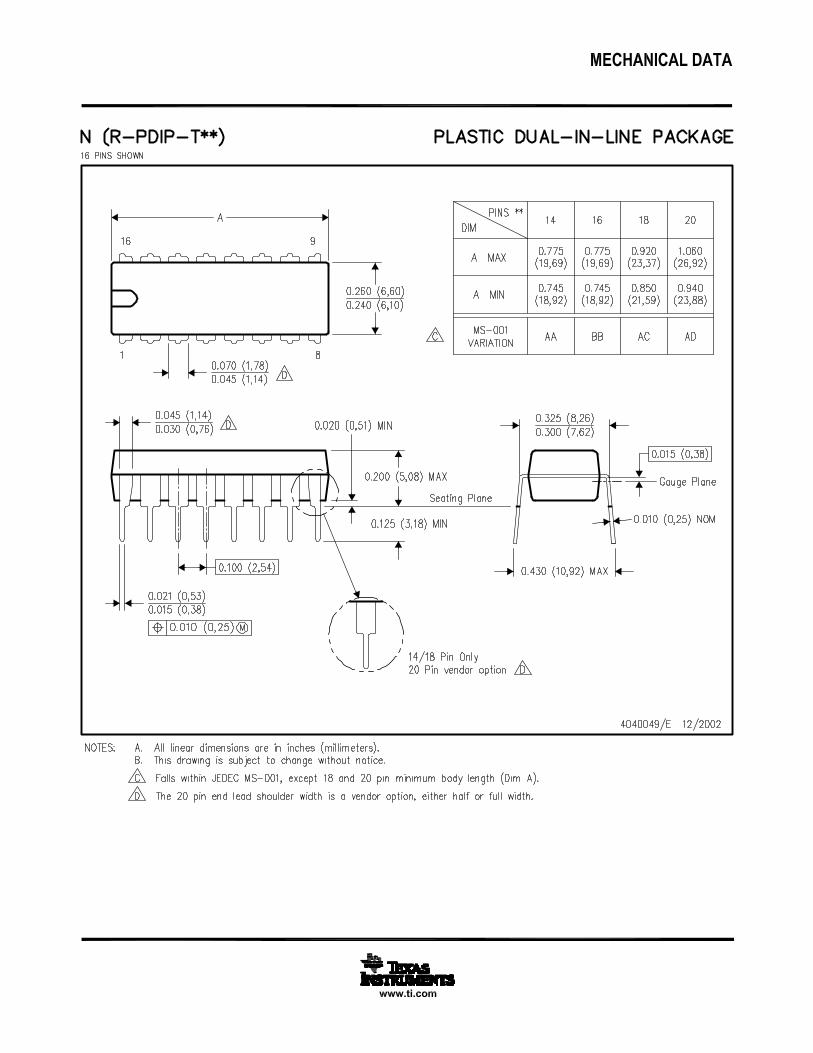

IMPORTANT NOTICE
Texas Instruments Incorporated (TI) reserves the right to make corrections, enhancements, improvements and other changes to itssemiconductor products and services per JESD46, latest issue, and to discontinue any product or service per JESD48, latest issue. Buyersshould obtain the latest relevant information before placing orders and should verify that such information is current and complete.TI’s published terms of sale for semiconductor products (http://www.ti.com/sc/docs/stdterms.htm) apply to the sale of packaged integratedcircuit products that TI has qualified and released to market. Additional terms may apply to the use or sale of other types of TI products andservices.Reproduction of significant portions of TI information in TI data sheets is permissible only if reproduction is without alteration and isaccompanied by all associated warranties, conditions, limitations, and notices. TI is not responsible or liable for such reproduceddocumentation. Information of third parties may be subject to additional restrictions. Resale of TI products or services with statementsdifferent from or beyond the parameters stated by TI for that product or service voids all express and any implied warranties for theassociated TI product or service and is an unfair and deceptive business practice. TI is not responsible or liable for any such statements.Buyers and others who are developing systems that incorporate TI products (collectively, “Designers”) understand and agree that Designersremain responsible for using their independent analysis, evaluation and judgment in designing their applications and that Designers havefull and exclusive responsibility to assure the safety of Designers' applications and compliance of their applications (and of all TI productsused in or for Designers’ applications) with all applicable regulations, laws and other applicable requirements. Designer represents that, withrespect to their applications, Designer has all the necessary expertise to create and implement safeguards that (1) anticipate dangerousconsequences of failures, (2) monitor failures and their consequences, and (3) lessen the likelihood of failures that might cause harm andtake appropriate actions. Designer agrees that prior to using or distributing any applications that include TI products, Designer willthoroughly test such applications and the functionality of such TI products as used in such applications.TI’s provision of technical, application or other design advice, quality characterization, reliability data or other services or information,including, but not limited to, reference designs and materials relating to evaluation modules, (collectively, “TI Resources”) are intended toassist designers who are developing applications that incorporate TI products; by downloading, accessing or using TI Resources in anyway, Designer (individually or, if Designer is acting on behalf of a company, Designer’s company) agrees to use any particular TI Resourcesolely for this purpose and subject to the terms of this Notice.TI’s provision of TI Resources does not expand or otherwise alter TI’s applicable published warranties or warranty disclaimers for TIproducts, and no additional obligations or liabilities arise from TI providing such TI Resources. TI reserves the right to make corrections,enhancements, improvements and other changes to its TI Resources. TI has not conducted any testing other than that specificallydescribed in the published documentation for a particular TI Resource.Designer is authorized to use, copy and modify any individual TI Resource only in connection with the development of applications thatinclude the TI product(s) identified in such TI Resource. NO OTHER LICENSE, EXPRESS OR IMPLIED, BY ESTOPPEL OR OTHERWISETO ANY OTHER TI INTELLECTUAL PROPERTY RIGHT, AND NO LICENSE TO ANY TECHNOLOGY OR INTELLECTUAL PROPERTYRIGHT OF TI OR ANY THIRD PARTY IS GRANTED HEREIN, including but not limited to any patent right, copyright, mask work right, orother intellectual property right relating to any combination, machine, or process in which TI products or services are used. Informationregarding or referencing third-party products or services does not constitute a license to use such products or services, or a warranty orendorsement thereof. Use of TI Resources may require a license from a third party under the patents or other intellectual property of thethird party, or a license from TI under the patents or other intellectual property of TI.TI RESOURCES ARE PROVIDED “AS IS” AND WITH ALL FAULTS. TI DISCLAIMS ALL OTHER WARRANTIES ORREPRESENTATIONS, EXPRESS OR IMPLIED, REGARDING RESOURCES OR USE THEREOF, INCLUDING BUT NOT LIMITED TOACCURACY OR COMPLETENESS, TITLE, ANY EPIDEMIC FAILURE WARRANTY AND ANY IMPLIED WARRANTIES OFMERCHANTABILITY, FITNESS FOR A PARTICULAR PURPOSE, AND NON-INFRINGEMENT OF ANY THIRD PARTY INTELLECTUALPROPERTY RIGHTS. TI SHALL NOT BE LIABLE FOR AND SHALL NOT DEFEND OR INDEMNIFY DESIGNER AGAINST ANY CLAIM,INCLUDING BUT NOT LIMITED TO ANY INFRINGEMENT CLAIM THAT RELATES TO OR IS BASED ON ANY COMBINATION OFPRODUCTS EVEN IF DESCRIBED IN TI RESOURCES OR OTHERWISE. IN NO EVENT SHALL TI BE LIABLE FOR ANY ACTUAL,DIRECT, SPECIAL, COLLATERAL, INDIRECT, PUNITIVE, INCIDENTAL, CONSEQUENTIAL OR EXEMPLARY DAMAGES INCONNECTION WITH OR ARISING OUT OF TI RESOURCES OR USE THEREOF, AND REGARDLESS OF WHETHER TI HAS BEENADVISED OF THE POSSIBILITY OF SUCH DAMAGES.Unless TI has explicitly designated an individual product as meeting the requirements of a particular industry standard (e.g., ISO/TS 16949and ISO 26262), TI is not responsible for any failure to meet such industry standard requirements.Where TI specifically promotes products as facilitating functional safety or as compliant with industry functional safety standards, suchproducts are intended to help enable customers to design and create their own applications that meet applicable functional safety standardsand requirements. Using products in an application does not by itself establish any safety features in the application. Designers mustensure compliance with safety-related requirements and standards applicable to their applications. Designer may not use any TI products inlife-critical medical equipment unless authorized officers of the parties have executed a special contract specifically governing such use.Life-critical medical equipment is medical equipment where failure of such equipment would cause serious bodily injury or death (e.g., lifesupport, pacemakers, defibrillators, heart pumps, neurostimulators, and implantables). Such equipment includes, without limitation, allmedical devices identified by the U.S. Food and Drug Administration as Class III devices and equivalent classifications outside the U.S.TI may expressly designate certain products as completing a particular qualification (e.g., Q100, Military Grade, or Enhanced Product).Designers agree that it has the necessary expertise to select the product with the appropriate qualification designation for their applicationsand that proper product selection is at Designers’ own risk. Designers are solely responsible for compliance with all legal and regulatoryrequirements in connection with such selection.Designer will fully indemnify TI and its representatives against any damages, costs, losses, and/or liabilities arising out of Designer’s non-compliance with the terms and provisions of this Notice.
Mailing Address: Texas Instruments, Post Office Box 655303, Dallas, Texas 75265Copyright © 2017, Texas Instruments Incorporated