Embed Size (px)
Citation preview
1SPRZ439F–January 2017–Revised April 2020Submit Documentation Feedback
Copyright © 2017–2020, Texas Instruments Incorporated
TMS320F28004x MCUs Silicon Errata Silicon Revisions B, A, 0
Silicon ErrataSPRZ439F–January 2017–Revised April 2020
TMS320F28004x MCUs Silicon ErrataSilicon Revisions B, A, 0
1 IntroductionThis document describes the silicon updates to the functional specifications for the TMS320F28004x(F28004x) microcontrollers (MCUs).
The updates are applicable to the following:• 100-pin Low-Profile Quad Flatpack, PZ Suffix• 64-pin Low-Profile Quad Flatpack, PM Suffix• 56-pin Very Thin Quad Flatpack No-Lead, RSH Suffix
2 Device and Development Support Tool NomenclatureTo designate the stages in the product development cycle, TI assigns prefixes to the part numbers of allTMS320 MCU devices and support tools. Each TMS320™ MCU commercial family member has one oftwo prefixes: TMX or TMS (for example, TMS320F280049). Texas Instruments recommends two of threepossible prefix designators for its support tools: TMDX and TMDS. These prefixes represent evolutionarystages of product development from engineering prototypes (with TMX for devices and TMDX for tools)through fully qualified production devices and tools (with TMS for devices and TMDS for tools).
TMX Experimental device that is not necessarily representative of the final device's electricalspecifications
TMS Fully qualified production device
Support tool development evolutionary flow:
TMDX Development-support product that has not yet completed Texas Instruments internalqualification testing
TMDS Fully qualified development-support product
TMX devices and TMDX development-support tools are shipped against the following disclaimer:"Developmental product is intended for internal evaluation purposes."
TMS devices and TMDS development-support tools have been characterized fully, and the quality andreliability of the device have been demonstrated fully. TI's standard warranty applies.
Predictions show that prototype devices (TMX) have a greater failure rate than the standard productiondevices. Texas Instruments recommends that these devices not be used in any production systembecause their expected end-use failure rate still is undefined. Only qualified production devices are to beused.
TI device nomenclature also includes a suffix with the device family name. This suffix indicates thepackage type (for example, PZ) and temperature range (for example, S).
YMLLLLS
YMLLLL
S$$
#
G4
Lot Trace Code
2-Digit Year/Month CodeAssembly LotAssembly Site CodeWafer Fab Code (one or two characters) as applicableSilicon Revision Code
Green (Low Halogen and RoHS-compliant)
=
=====
=
G4
F280049
$$#−YMLLLLS
RSHS
TI
PackagePin 1
YMLLLLS
YMLLLL
S980
$$#
G4
Lot Trace Code
2-Digit Year/Month CodeAssembly LotAssembly Site CodeTI E.I.A. CodeWafer Fab Code (one or two characters) as applicableSilicon Revision Code
Green (Low Halogen and RoHS-compliant)
=
======
=
G4
980
$$#−YMLLLLS
F280049PZS
PackagePin 1
G4
980
$$#−YMLLLLS
F280049PMS
PackagePin 1
Device Markings www.ti.com
2 SPRZ439F–January 2017–Revised April 2020Submit Documentation Feedback
Copyright © 2017–2020, Texas Instruments Incorporated
TMS320F28004x MCUs Silicon Errata Silicon Revisions B, A, 0
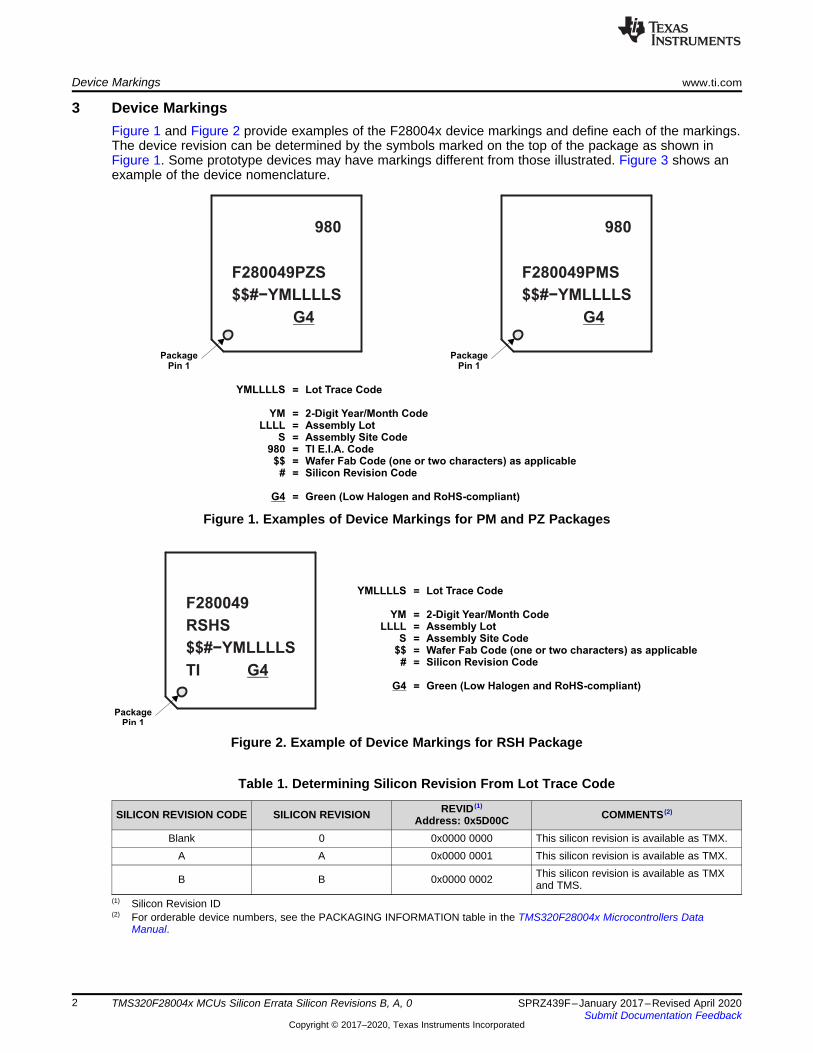
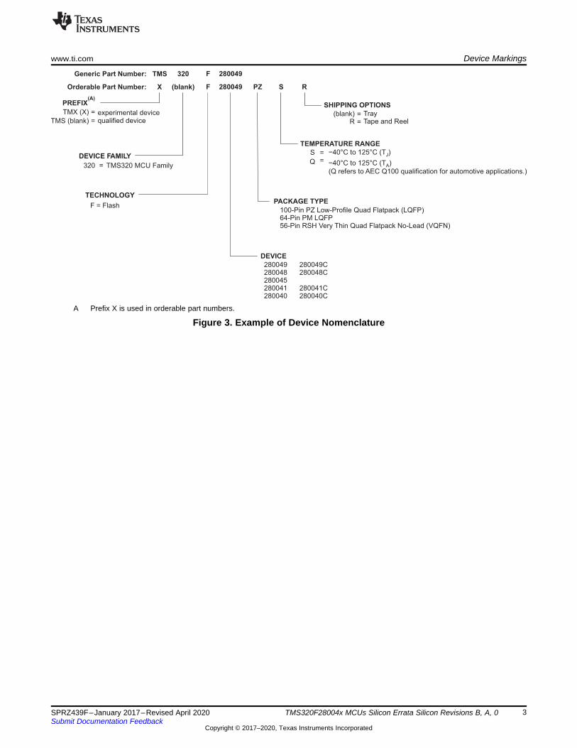
3 Device MarkingsFigure 1 and Figure 2 provide examples of the F28004x device markings and define each of the markings.The device revision can be determined by the symbols marked on the top of the package as shown inFigure 1. Some prototype devices may have markings different from those illustrated. Figure 3 shows anexample of the device nomenclature.
Figure 1. Examples of Device Markings for PM and PZ Packages
Figure 2. Example of Device Markings for RSH Package
(1) Silicon Revision ID(2) For orderable device numbers, see the PACKAGING INFORMATION table in the TMS320F28004x Microcontrollers Data
Manual.
Table 1. Determining Silicon Revision From Lot Trace Code
SILICON REVISION CODE SILICON REVISION REVID (1)
Address: 0x5D00C COMMENTS (2)
Blank 0 0x0000 0000 This silicon revision is available as TMX.A A 0x0000 0001 This silicon revision is available as TMX.
B B 0x0000 0002 This silicon revision is available as TMXand TMS.
TECHNOLOGY
F = FlashPACKAGE TYPE
100-Pin PZ Low-Profile Quad Flatpack (LQFP)64-Pin PM LQFP56-Pin RSH Very Thin Quad Flatpack No-Lead (VQFN)
TEMPERATURE RANGE
−40°C to 125°C (T )J
−40°C to 125°C (T )A
(Q refers to AEC Q100 qualification for automotive applications.)
S
Q
==
SHIPPING OPTIONS
TrayTape and Reel
(blank)R
==
PREFIX(A)
TMX (X) = experimental deviceTMS (blank) = qualified device
F 280049 PZ S RX (blank)
F 280049TMSGeneric Part Number:
Orderable Part Number:
320
DEVICE FAMILY
320 = TMS320 MCU Family
DEVICE
280049280048280045280041280040
280049C280048C
280041C280040C
www.ti.com Device Markings
3SPRZ439F–January 2017–Revised April 2020Submit Documentation Feedback
Copyright © 2017–2020, Texas Instruments Incorporated
TMS320F28004x MCUs Silicon Errata Silicon Revisions B, A, 0
A Prefix X is used in orderable part numbers.
Figure 3. Example of Device Nomenclature
Usage Notes and Known Design Exceptions to Functional Specifications www.ti.com
4 SPRZ439F–January 2017–Revised April 2020Submit Documentation Feedback
Copyright © 2017–2020, Texas Instruments Incorporated
TMS320F28004x MCUs Silicon Errata Silicon Revisions B, A, 0
4 Usage Notes and Known Design Exceptions to Functional Specifications
4.1 Usage NotesUsage notes highlight and describe particular situations where the device's behavior may not matchpresumed or documented behavior. This may include behaviors that affect device performance orfunctional correctness. These usage notes will be incorporated into future documentation updates for thedevice (such as the device-specific data sheet), and the behaviors they describe will not be altered infuture silicon revisions.
Table 2 shows which silicon revision(s) are affected by each usage note.
Table 2. List of Usage Notes
TITLESILICON REVISION(S)
AFFECTED0 A B
PIE: Spurious Nested Interrupt After Back-to-Back PIEACK Write and Manual CPU InterruptMask Clear Yes Yes Yes
FPU32 and VCU Back-to-Back Memory Accesses Yes Yes YesCaution While Using Nested Interrupts Yes Yes Yes
4.1.1 PIE: Spurious Nested Interrupt After Back-to-Back PIEACK Write and Manual CPU InterruptMask Clear
Revision(s) Affected: 0, A, B
Certain code sequences used for nested interrupts allow the CPU and PIE to enter an inconsistent statethat can trigger an unwanted interrupt. The conditions required to enter this state are:1. A PIEACK clear is followed immediately by a global interrupt enable (EINT or asm(" CLRC INTM")).2. A nested interrupt clears one or more PIEIER bits for its group.
Whether the unwanted interrupt is triggered depends on the configuration and timing of the otherinterrupts in the system. This is expected to be a rare or nonexistent event in most applications. If ithappens, the unwanted interrupt will be the first one in the nested interrupt's PIE group, and will betriggered after the nested interrupt re-enables CPU interrupts (EINT or asm(" CLRC INTM")).
Workaround: Add a NOP between the PIEACK write and the CPU interrupt enable. Example code isshown below.
//Bad interrupt nesting codePieCtrlRegs.PIEACK.all = 0xFFFF; //Enable nesting in the PIEEINT; //Enable nesting in the CPU
//Good interrupt nesting codePieCtrlRegs.PIEACK.all = 0xFFFF; //Enable nesting in the PIEasm(" NOP"); //Wait for PIEACK to exit the pipelineEINT; //Enable nesting in the CPU
www.ti.com Usage Notes and Known Design Exceptions to Functional Specifications
5SPRZ439F–January 2017–Revised April 2020Submit Documentation Feedback
Copyright © 2017–2020, Texas Instruments Incorporated
TMS320F28004x MCUs Silicon Errata Silicon Revisions B, A, 0
4.1.2 FPU32 and VCU Back-to-Back Memory AccessesRevision(s) Affected: 0, A, B
This usage note applies when a VCU memory access and an FPU memory access occur back-to-back.There are three cases:
Case 1. Back-to-back memory reads: one read performed by a VCU instruction (VMOV32) and one readperformed by an FPU32 instruction (MOV32).
If an R1 pipeline phase stall occurs during the first read, then the second read will latch the wrong data. Ifthe first instruction is not stalled during the R1 pipeline phase, then the second read will occur properly.
The order of the instructions—FPU followed by VCU or VCU followed by FPU—does not matter. Theaddress of the memory location accessed by either read does not matter.
Case 1 Workaround: Insert one instruction between the two back-to-back read instructions. Anyinstruction, except a VCU or FPU memory read, can be used.
Case 1, Example 1:
VMOV32 VR1,mem32 ; VCU memory readNOP ; Not a FPU/ VCU memory readMOV32 R0H,mem32 ; FPU memory read
Case 1, Example 2:
VMOV32 VR1,mem32 ; VCU memory readVMOV32 mem32, VR2 ; VCU memory writeMOV32 R0H,mem32 ; FPU memory read
Case 2. Back-to-back memory writes: one write performed by a VCU instruction (VMOV32) and one writeperformed by an FPU instruction (MOV32).
If a pipeline stall occurs during the first write, then the second write can corrupt the data. If the firstinstruction is not stalled in the write phase, then no corruption will occur.
The order of the instructions—FPU followed by VCU or VCU followed by FPU—does not matter. Theaddress of the memory location accessed by either write does not matter.
Case 2 Workaround: Insert two instructions between the back-to-back VCU and FPU writes. Anyinstructions, except VCU or FPU memory writes, can be used.
Case 2, Example 1:
VMOV32 mem32,VR0 ; VCU memory writeNOP ; Not a FPU/VCU memory writeNOP ; Not a FPU/VCU memory writeMOV32 mem32,R3H ; FPU memory write
Case 2, Example 2:
VMOV32 mem32,VR0 ; VCU memory writeVMOV32 VR1, mem32 ; VCU memory readNOPMOV32 mem32,R3H ; FPU memory write
Case 3. Back-to-back memory writes followed by a read or a memory read followed by a write. In thiscase, there is no interaction between the two instructions. No action is required.
Workaround: See Case 1 Workaround and Case 2 Workaround.
Usage Notes and Known Design Exceptions to Functional Specifications www.ti.com
6 SPRZ439F–January 2017–Revised April 2020Submit Documentation Feedback
Copyright © 2017–2020, Texas Instruments Incorporated
TMS320F28004x MCUs Silicon Errata Silicon Revisions B, A, 0
4.1.3 Caution While Using Nested InterruptsRevision(s) Affected: 0, A, B
If the user is enabling interrupts using the EINT instruction inside an interrupt service routine (ISR) in orderto use the nesting feature, then the user must disable the interrupts before exiting the ISR. Failing to do somay cause undefined behavior of CPU execution.
www.ti.com Usage Notes and Known Design Exceptions to Functional Specifications
7SPRZ439F–January 2017–Revised April 2020Submit Documentation Feedback
Copyright © 2017–2020, Texas Instruments Incorporated
TMS320F28004x MCUs Silicon Errata Silicon Revisions B, A, 0
4.2 Known Design Exceptions to Functional Specifications
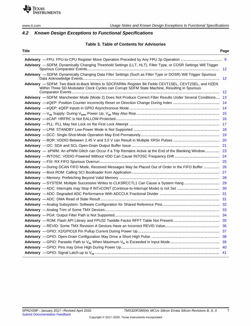
Table 3. Table of Contents for AdvisoriesTitle ...................................................................................................................................... Page
Advisory —FPU: FPU-to-CPU Register Move Operation Preceded by Any FPU 2p Operation .............................. 9Advisory —SDFM: Dynamically Changing Threshold Settings (LLT, HLT), Filter Type, or COSR Settings Will Trigger
Spurious Comparator Events................................................................................................. 12Advisory —SDFM: Dynamically Changing Data Filter Settings (Such as Filter Type or DOSR) Will Trigger Spurious
Data Acknowledge Events.................................................................................................... 12Advisory —SDFM: Two Back-to-Back Writes to SDCPARMx Register Bit Fields CEVT1SEL, CEVT2SEL, and HZEN
Within Three SD-Modulator Clock Cycles can Corrupt SDFM State Machine, Resulting in SpuriousComparator Events ............................................................................................................ 12
Advisory —SDFM: Manchester Mode (Mode 2) Does Not Produce Correct Filter Results Under Several Conditions... 13Advisory —eQEP: Position Counter Incorrectly Reset on Direction Change During Index .................................. 14Advisory —eQEP: eQEP Inputs in GPIO Asynchronous Mode .................................................................. 14Advisory —VDD Supply: During VDDIO Power Up, VDD May Also Rise............................................................. 15Advisory —eCAP: HRFRC is Not EALLOW-Protected............................................................................ 16Advisory —PLL: PLL May Not Lock on the First Lock Attempt .................................................................. 17Advisory —LPM: STANDBY Low-Power Mode is Not Supported ............................................................... 18Advisory —DCC: Single-Shot-Mode Operation May End Prematurely.......................................................... 19Advisory —BOR: VDDIO Between 2.45 V and 3.0 V can Result in Multiple XRSn Pulses .................................. 20Advisory —I2C: SDA and SCL Open-Drain Output Buffer Issue ................................................................ 21Advisory — ePWM: An ePWM Glitch can Occur if a Trip Remains Active at the End of the Blanking Window........... 23Advisory —INTOSC: VDDIO Powered Without VDD Can Cause INTOSC Frequency Drift ................................. 24Advisory —FSI: RX FIFO Spurious Overrun........................................................................................ 25Advisory —During DCAN FIFO Mode, Received Messages May be Placed Out of Order in the FIFO Buffer ............ 26Advisory —Boot ROM: Calling SCI Bootloader from Application ................................................................ 27Advisory —Memory: Prefetching Beyond Valid Memory ......................................................................... 28Advisory —SYSTEM: Multiple Successive Writes to CLKSRCCTL1 Can Cause a System Hang .......................... 29Advisory —ADC: Interrupts may Stop if INTxCONT (Continue-to-Interrupt Mode) is not Set ............................... 30Advisory —ADC: Degraded ADC Performance With ADCCLK Fractional Divider ............................................ 31Advisory —ADC: DMA Read of Stale Result ....................................................................................... 31Advisory —Analog Subsystem: Software Configuration for Shared Reference Pins.......................................... 32Advisory —Analog Trim of Some TMX Devices.................................................................................... 33Advisory —PGA: Output Filter Path is Not Supported............................................................................. 34Advisory —ROM: Flash API Library and FPU32 Twiddle Factor RFFT Table Not Present .................................. 35Advisory —REVID: Some TMX Revision A Devices Have an Incorrect REVID Value........................................ 36Advisory —GPIO: X2/GPIO18 Pin Pullup Current During Power Up............................................................ 37Advisory —GPIO: Open-Drain Configuration May Drive a Short High Pulse .................................................. 38Advisory —GPIO: Parasitic Path to VSS When Maximum VIH is Exceeded in Input Mode .................................... 39Advisory —GPIO: Pins may Drive High During Power Up........................................................................ 40Advisory —GPIO: Signal Latch-up to VSS ........................................................................................... 41
Usage Notes and Known Design Exceptions to Functional Specifications www.ti.com
8 SPRZ439F–January 2017–Revised April 2020Submit Documentation Feedback
Copyright © 2017–2020, Texas Instruments Incorporated
TMS320F28004x MCUs Silicon Errata Silicon Revisions B, A, 0
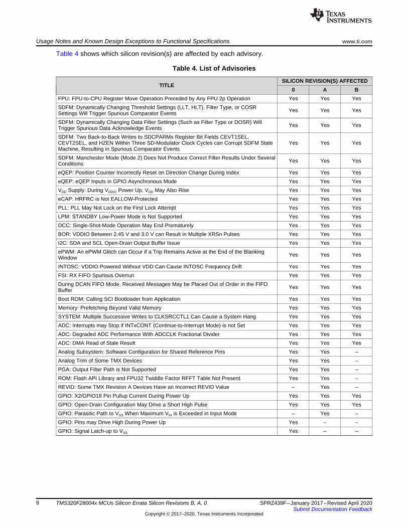
Table 4 shows which silicon revision(s) are affected by each advisory.
Table 4. List of Advisories
TITLESILICON REVISION(S) AFFECTED
0 A BFPU: FPU-to-CPU Register Move Operation Preceded by Any FPU 2p Operation Yes Yes YesSDFM: Dynamically Changing Threshold Settings (LLT, HLT), Filter Type, or COSRSettings Will Trigger Spurious Comparator Events Yes Yes Yes
SDFM: Dynamically Changing Data Filter Settings (Such as Filter Type or DOSR) WillTrigger Spurious Data Acknowledge Events Yes Yes Yes
SDFM: Two Back-to-Back Writes to SDCPARMx Register Bit Fields CEVT1SEL,CEVT2SEL, and HZEN Within Three SD-Modulator Clock Cycles can Corrupt SDFM StateMachine, Resulting in Spurious Comparator Events
Yes Yes Yes
SDFM: Manchester Mode (Mode 2) Does Not Produce Correct Filter Results Under SeveralConditions Yes Yes Yes
eQEP: Position Counter Incorrectly Reset on Direction Change During Index Yes Yes YeseQEP: eQEP Inputs in GPIO Asynchronous Mode Yes Yes YesVDD Supply: During VDDIO Power Up, VDD May Also Rise Yes Yes YeseCAP: HRFRC is Not EALLOW-Protected Yes Yes YesPLL: PLL May Not Lock on the First Lock Attempt Yes Yes YesLPM: STANDBY Low-Power Mode is Not Supported Yes Yes YesDCC: Single-Shot-Mode Operation May End Prematurely Yes Yes YesBOR: VDDIO Between 2.45 V and 3.0 V can Result in Multiple XRSn Pulses Yes Yes YesI2C: SDA and SCL Open-Drain Output Buffer Issue Yes Yes YesePWM: An ePWM Glitch can Occur if a Trip Remains Active at the End of the BlankingWindow Yes Yes Yes
INTOSC: VDDIO Powered Without VDD Can Cause INTOSC Frequency Drift Yes Yes YesFSI: RX FIFO Spurious Overrun Yes Yes YesDuring DCAN FIFO Mode, Received Messages May be Placed Out of Order in the FIFOBuffer Yes Yes Yes
Boot ROM: Calling SCI Bootloader from Application Yes Yes YesMemory: Prefetching Beyond Valid Memory Yes Yes YesSYSTEM: Multiple Successive Writes to CLKSRCCTL1 Can Cause a System Hang Yes Yes YesADC: Interrupts may Stop if INTxCONT (Continue-to-Interrupt Mode) is not Set Yes Yes YesADC: Degraded ADC Performance With ADCCLK Fractional Divider Yes Yes YesADC: DMA Read of Stale Result Yes Yes YesAnalog Subsystem: Software Configuration for Shared Reference Pins Yes Yes –Analog Trim of Some TMX Devices Yes Yes –PGA: Output Filter Path is Not Supported Yes Yes –ROM: Flash API Library and FPU32 Twiddle Factor RFFT Table Not Present Yes Yes –REVID: Some TMX Revision A Devices Have an Incorrect REVID Value – Yes –GPIO: X2/GPIO18 Pin Pullup Current During Power Up Yes Yes YesGPIO: Open-Drain Configuration May Drive a Short High Pulse Yes Yes YesGPIO: Parasitic Path to VSS When Maximum VIH is Exceeded in Input Mode – Yes –GPIO: Pins may Drive High During Power Up Yes – –GPIO: Signal Latch-up to VSS Yes – –
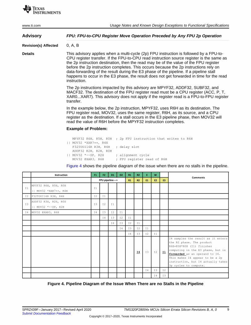
Instruction F1 F2 D1 D2 R1 R2 E W
R1 R2 E1 E2 E3
MPYF32 R6H, R5H, R0H
|| MOV32 *XAR7++, R4H
I2 F32TOUI16R R3H, R4H I2 I1
ADDF32 R3H, R2H, R0H
|| MOV32 *--SP, R2H
I4 MOV32 @XAR3, R6H I4 I3 I2 I1
I4 I3 I2 I1
I4 I3 I2 I1
I4 I3 I2 I1
I4 I3 I2 I1
I4 I3 I2 I1
I4 samples the result as it enters
the R2 phase. The product
R6H=R5H*R0H (I1) finishes
computing in the E3 phase, but is
forwarded as an operand to I4.
This makes I4 appear to be a 2p
instruction, but I4 actually takes
3p cycles to compute.
I4 I3 I2
I4 I3
I3
CommentsFPU pipeline--->
I1 I1
I3 I2 I1
www.ti.com Usage Notes and Known Design Exceptions to Functional Specifications
9SPRZ439F–January 2017–Revised April 2020Submit Documentation Feedback
Copyright © 2017–2020, Texas Instruments Incorporated
TMS320F28004x MCUs Silicon Errata Silicon Revisions B, A, 0
Advisory FPU: FPU-to-CPU Register Move Operation Preceded by Any FPU 2p Operation
Revision(s) Affected 0, A, B
Details This advisory applies when a multi-cycle (2p) FPU instruction is followed by a FPU-to-CPU register transfer. If the FPU-to-CPU read instruction source register is the same asthe 2p instruction destination, then the read may be of the value of the FPU registerbefore the 2p instruction completes. This occurs because the 2p instructions rely ondata-forwarding of the result during the E3 phase of the pipeline. If a pipeline stallhappens to occur in the E3 phase, the result does not get forwarded in time for the readinstruction.
The 2p instructions impacted by this advisory are MPYF32, ADDF32, SUBF32, andMACF32. The destination of the FPU register read must be a CPU register (ACC, P, T,XAR0...XAR7). This advisory does not apply if the register read is a FPU-to-FPU registertransfer.
In the example below, the 2p instruction, MPYF32, uses R6H as its destination. TheFPU register read, MOV32, uses the same register, R6H, as its source, and a CPUregister as the destination. If a stall occurs in the E3 pipeline phase, then MOV32 willread the value of R6H before the MPYF32 instruction completes.
Example of Problem:
MPYF32 R6H, R5H, R0H ; 2p FPU instruction that writes to R6H|| MOV32 *XAR7++, R4H
F32TOUI16R R3H, R4H ; delay slotADDF32 R2H, R2H, R0H
|| MOV32 *--SP, R2H ; alignment cycleMOV32 @XAR3, R6H ; FPU register read of R6H
Figure 4 shows the pipeline diagram of the issue when there are no stalls in the pipeline.
Figure 4. Pipeline Diagram of the Issue When There are no Stalls in the Pipeline
Instruction F1 F2 D1 D2 R1 R2 E W
R1 R2 E1 E2 E3
MPYF32 R6H, R5H, R0H
|| MOV32 *XAR7++, R4H
I2 F32TOUI16R R3H, R4H I2 I1
ADDF32 R3H, R2H, R0H
|| MOV32 *--SP, R2H
I4 MOV32 @XAR3, R6H I4 I3 I2 I1
I4 I3 I2 I1
I4 I3 I2 I1
I4 I3 I2 I1
I4 I3 I2 I1
I4 I3 I2I1
(STALL)
I4 samples the result as it enters
the R2 phase, but I1 is stalled in
E3 and is unable to forward the
product of R5H*R0H to I4 (R6H does
not have the product yet due to a
design bug). So, I4 reads the old
value of R6H.
I4 I3 I2 I1
There is no change in the pipeline
as it was stalled in the previous
cycle. I4 had already sampled the
old value of R6H in the previous
cycle.
I4 I3 I2 Stall over
I3 I3 I2 I1
CommentsFPU pipeline-->
I1 I1
Usage Notes and Known Design Exceptions to Functional Specifications www.ti.com
10 SPRZ439F–January 2017–Revised April 2020Submit Documentation Feedback
Copyright © 2017–2020, Texas Instruments Incorporated
TMS320F28004x MCUs Silicon Errata Silicon Revisions B, A, 0
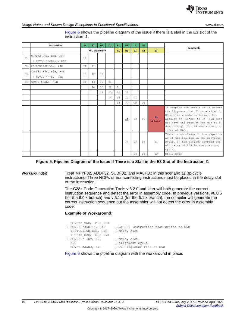
Figure 5 shows the pipeline diagram of the issue if there is a stall in the E3 slot of theinstruction I1.
Figure 5. Pipeline Diagram of the Issue if There is a Stall in the E3 Slot of the Instruction I1
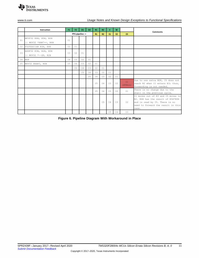
Workaround(s) Treat MPYF32, ADDF32, SUBF32, and MACF32 in this scenario as 3p-cycleinstructions. Three NOPs or non-conflicting instructions must be placed in the delay slotof the instruction.
The C28x Code Generation Tools v.6.2.0 and later will both generate the correctinstruction sequence and detect the error in assembly code. In previous versions, v6.0.5(for the 6.0.x branch) and v.6.1.2 (for the 6.1.x branch), the compiler will generate thecorrect instruction sequence but the assembler will not detect the error in assemblycode.
Example of Workaround:
MPYF32 R6H, R5H, R0H|| MOV32 *XAR7++, R4H ; 3p FPU instruction that writes to R6H
F32TOUI16R R3H, R4H ; delay slotADDF32 R2H, R2H, R0H
|| MOV32 *--SP, R2H ; delay slotNOP ; alignment cycleMOV32 @XAR3, R6H ; FPU register read of R6H
Figure 6 shows the pipeline diagram with the workaround in place.
Instruction F1 F2 D1 D2 R1 R2 E W
R1 R2 E1 E2 E3
MPYF32 R6H, R5H, R0H
|| MOV32 *XAR7++, R4H
I2 F32TOUI16R R3H, R4H I2 I1
ADDF32 R3H, R2H, R0H
|| MOV32 *--SP, R2H
I4 NOP I4 I3 I2 I1
I5 MOV32 @XAR3, R6H I5 I4 I3 I2 I1
I5 I4 I3 I2 I1
I5 I4 I3 I2 I1
I5 I4 I3 I2 I1
I5 I4 I3 I2I1
(STALL)
Due to one extra NOP, I5 does not
reach R2 when I1 enters E3; thus,
forwarding is not needed.
I5 I4 I3 I2 I1There is no change due to the
stall in the previous cycle.
I5 I4 I3 I2
I1 moves out of E3 and I5 moves to
R2. R6H has the result of R5H*R0H
and is read by I5. There is no
need to forward the result in this
case.
I5 I4 I3
I3 I3 I2 I1
CommentsFPU pipeline-->
I1 I1
www.ti.com Usage Notes and Known Design Exceptions to Functional Specifications
11SPRZ439F–January 2017–Revised April 2020Submit Documentation Feedback
Copyright © 2017–2020, Texas Instruments Incorporated
TMS320F28004x MCUs Silicon Errata Silicon Revisions B, A, 0
Figure 6. Pipeline Diagram With Workaround in Place
Usage Notes and Known Design Exceptions to Functional Specifications www.ti.com
12 SPRZ439F–January 2017–Revised April 2020Submit Documentation Feedback
Copyright © 2017–2020, Texas Instruments Incorporated
TMS320F28004x MCUs Silicon Errata Silicon Revisions B, A, 0
Advisory SDFM: Dynamically Changing Threshold Settings (LLT, HLT), Filter Type, or COSRSettings Will Trigger Spurious Comparator Events
Revision(s) Affected 0, A, B
Details When SDFM comparator settings—such as filter type, lower/upper threshold, orcomparator OSR (COSR) settings—are dynamically changed during run time, spuriouscomparator events will be triggered. The spurious comparator event will trigger acorresponding CPU interrupt, CLA task, ePWM X-BAR events, and GPIO output X-BARevents if configured appropriately.
Workaround(s) When comparator settings need to be changed dynamically, follow the procedure belowto ensure spurious comparator events do not generate a CPU interrupt, CLA task, orX-BAR events (ePWM X-BAR/GPIO output X-BAR events):1. Disable the comparator filter.2. Delay for at least a latency of the comparator filter + 3 SD-Cx clock cycles.3. Change comparator filter settings such as filter type, COSR, or lower/upper threshold.4. Delay for at least a latency of the comparator filter + 5 SD-Cx clock cycles.5. Enable the comparator filter.
Advisory SDFM: Dynamically Changing Data Filter Settings (Such as Filter Type or DOSR)Will Trigger Spurious Data Acknowledge Events
Revision(s) Affected 0, A, B
Details When SDFM data settings—such as filter type or DOSR settings—are dynamicallychanged during run time, spurious data-filter-ready events will be triggered. The spuriousdata-ready event will trigger a corresponding CPU interrupt, CLA task, and DMA trigger ifconfigured appropriately.
Workaround(s) When SDFM data filter settings need to be changed dynamically, follow the procedurebelow to ensure spurious data-filter-ready events are not generated:1. Disable the data filter.2. Delay for at least a latency of the data filter + 3 SD-Cx clock cycles.3. Change data filter settings such as filter type and DOSR.4. Delay for at least a latency of the data filter + 5 SD-Cx clock cycles.5. Enable the data filter.
Advisory SDFM: Two Back-to-Back Writes to SDCPARMx Register Bit Fields CEVT1SEL,CEVT2SEL, and HZEN Within Three SD-Modulator Clock Cycles can Corrupt SDFMState Machine, Resulting in Spurious Comparator Events
Revision(s) Affected 0, A, B
Details Back-to-back writes to SDCPARMx register bit fields CEVT1SEL, CEVT2SEL, andHZEN within three SD-modulator clock cycles can potentially corrupt the SDFM statemachine, resulting in spurious comparator events, which can potentially trigger CPUinterrupts, CLA tasks, ePWM XBAR events, and GPIO output X-BAR events ifconfigured appropriately.
Workaround(s) Avoid back-to-back writes within three SD-modulator clock cycles or have theSDCPARMx register bit fields configured in one register write.
www.ti.com Usage Notes and Known Design Exceptions to Functional Specifications
13SPRZ439F–January 2017–Revised April 2020Submit Documentation Feedback
Copyright © 2017–2020, Texas Instruments Incorporated
TMS320F28004x MCUs Silicon Errata Silicon Revisions B, A, 0
Advisory SDFM: Manchester Mode (Mode 2) Does Not Produce Correct Filter Results UnderSeveral Conditions
Revision(s) Affected 0, A, B
Details The Manchester decoding algorithm samples the Manchester bitstream with SYSCLK ina calibration window of 1024 SDx_Dy signal transitions. The derived clock from theManchester bitstream is used to sample for data in the subsequent calibration windowcycle.
There are several scenarios that can cause large errors in the filter results:• Any single noise event on SDx_Dy can corrupt the decoded Manchester clock and
cause subsequent data to be sampled at an incorrect frequency.• If the Manchester bitstream clock rate is a near exact integer multiple of SYSCLK,
then an occasional Manchester bit can be skipped when the phases of theManchester stream and internal SYSCLK drift past each other in phase before thenext 1024 transition calibration window becomes effective. Deviations in duty cyclefrom 50% of the Manchester clock also need to be accounted for to ensure the longerManchester pulses are not an integer multiple of SYSCLK. This situation can beunavoidable if the clock sources for either the SD modulator or this device have awide variation since a wide range of keep out frequencies become problematic
• If the Manchester edge delay variation between rising and falling (duty cycle of thebitstream) is greater than one SYSCLK, then the SDFM clock decode algorithm canincorrectly identify the clock period as shorter than it is.
Workaround(s) The workarounds available are:• Avoid using Manchester mode and consider using Mode 0, which provides the best
filter performance under noisy conditions. This is the recommended workaround.• Avoid any noise on the Manchester bitstream and avoid integer multiples of SYSCLK
for the selected Manchester clock source. A precision clock source for the modulatorand this device must be used.
• Ensure rising and falling edge delays (high and low pulses) are within one SYSCLKof each other in length.
• Design an application-level algorithm that is robust against occasional incorrectSDFM results.
Usage Notes and Known Design Exceptions to Functional Specifications www.ti.com
14 SPRZ439F–January 2017–Revised April 2020Submit Documentation Feedback
Copyright © 2017–2020, Texas Instruments Incorporated
TMS320F28004x MCUs Silicon Errata Silicon Revisions B, A, 0
Advisory eQEP: Position Counter Incorrectly Reset on Direction Change During Index
Revision(s) Affected 0, A, B
Details While using the PCRM = 0 configuration, if the direction change occurs when the indexinput is active, the position counter (QPOSCNT) could be reset erroneously, resulting inan unexpected change in the counter value. This could result in a change of up to±4 counts from the expected value of the position counter and lead to unexpectedsubsequent setting of the error flags.
While using the PCRM = 0 configuration [that is, Position Counter Reset on Index Event(QEPCTL[PCRM] = 00)], if the index event occurs during the forward movement, thenthe position counter is reset to 0 on the next eQEP clock. If the index event occursduring the reverse movement, then the position counter is reset to the value in theQPOSMAX register on the next eQEP clock. The eQEP peripheral records theoccurrence of the first index marker (QEPSTS[FIMF]) and direction on the first indexevent marker (QEPSTS[FIDF]) in QEPSTS registers. It also remembers the quadratureedge on the first index marker so that same relative quadrature transition is used forindex event reset operation.
If the direction change occurs while the index pulse is active, the module would stillcontinue to look for the relative quadrature transition for performing the position counterreset. This results in an unexpected change in the position counter value.
The next index event without a simultaneous direction change will reset the counterproperly and work as expected.
Workaround(s) Do not use the PCRM = 0 configuration if the direction change could occur while theindex is active and the resultant change of the position counter value could affect theapplication.
Other options for performing position counter reset, if appropriate for the application[such as Index Event Initialization (IEI)], do not have this issue.
Advisory eQEP: eQEP Inputs in GPIO Asynchronous Mode
Revision(s) Affected 0, A, B
Details If any of the eQEP input pins are configured for GPIO asynchronous input mode via theGPxQSELn registers, the eQEP module may not operate properly because the eQEPperipheral assumes the presence of external synchronization to SYSCLKOUT on inputsto the module. For example, QPOSCNT may not reset or latch properly, and pulses onthe input pins may be missed.
For proper operation of the eQEP module, input GPIO pins should be configured via theGPxQSELn registers for synchronous input mode (with or without qualification), which isthe default state of the GPxQSEL registers at reset. All existing eQEP peripheralexamples supplied by TI also configure the GPIO inputs for synchronous input mode.
The asynchronous mode should not be used for eQEP module input pins.
Workaround(s) Configure GPIO inputs configured as eQEP pins for non-asynchronous mode (anyGPxQSELn register option except “11b = Asynchronous”).
www.ti.com Usage Notes and Known Design Exceptions to Functional Specifications
15SPRZ439F–January 2017–Revised April 2020Submit Documentation Feedback
Copyright © 2017–2020, Texas Instruments Incorporated
TMS320F28004x MCUs Silicon Errata Silicon Revisions B, A, 0
Advisory VDD Supply: During VDDIO Power Up, VDD May Also Rise
Revision(s) Affected 0, A, B
Details A leakage current from VDDIO to VDD is present when the VDD supply is belowapproximately 0.5 V. This causes the VDD voltage to rise to approximately 0.5 V whenVDDIO is powered. This is observed when the device is configured to use either theinternal VREG (VREGENZ tied to VSS) or an external 1.2-V regulator (VREGENZ tied toVDDIO), and there is a significant delay (about 1 ms) between the power up of VDDIO andVDD from external regulators or the ramp time of VDDIO is greater than 1 ms when ininternal VREG mode.
This does not impact device functionality once the external 1.2-V or internal 1.2-V supplybegins to ramp. See the TMS320F28004x Microcontrollers Data Manual for powersequencing requirements.
Workaround(s) If this early voltage on VDD is a problem for system-level supervisor circuits, thenminimize the delay between ramping the 3.3-V VDDIO and 1.2-V VDD rails. If the internalVREG is used, decrease the ramp time of the 3.3-V VDDIO supply to 1 ms or less.
Usage Notes and Known Design Exceptions to Functional Specifications www.ti.com
16 SPRZ439F–January 2017–Revised April 2020Submit Documentation Feedback
Copyright © 2017–2020, Texas Instruments Incorporated
TMS320F28004x MCUs Silicon Errata Silicon Revisions B, A, 0
Advisory eCAP: HRFRC is Not EALLOW-Protected
Revision(s) Affected 0, A, B
Details The HRFRC register is not EALLOW-protected. Issuing the EALLOW and EDISinstructions to write to this register is not required. To enable software reuse on otherdevices where HRFRC is EALLOW-protected, using EALLOW and EDIS isrecommended.
Workaround(s) None
www.ti.com Usage Notes and Known Design Exceptions to Functional Specifications
17SPRZ439F–January 2017–Revised April 2020Submit Documentation Feedback
Copyright © 2017–2020, Texas Instruments Incorporated
TMS320F28004x MCUs Silicon Errata Silicon Revisions B, A, 0
Advisory PLL: PLL May Not Lock on the First Lock Attempt
Revision(s) Affected 0, A, B
Details The PLL may not start properly at device power up. The PLLSTS[LOCKS] bit is set, butthe PLL does not produce a clock.
Once the PLL has started properly, the PLL can be disabled and reenabled with noissues and will stay locked. However, the PLL lock problem could reoccur on asubsequent power-up cycle.
If the SYSPLL has not started properly and is selected as the CPU clock source, theCPU will stop executing instructions.
The occurrence rate of this transient issue is low. After an initial occurrence, this issuemay not be subsequently observed in the system again. Implementation of theworkaround reduces the rate of occurrence.
Workaround(s) TI recommends doing lock sequences in succession until the PLL is in locked statewhen the PLL is configured for the first time after power up. The lock sequence is:disable the PLL, start the PLL, wait for the LOCKS bit to set, and validate the PLLfrequency using the Dual Clock Comparator (DCC). After the PLL is observed to berunning, it can be selected as the CPU clock source.
TI recommends using the C2000Ware SysCtl_setClock() function, which also includesimplementation of this workaround, to set the PLL clock.
Details on DCC usage are in the C2000Ware SysCtl_IsPLLValid() function.
The workaround can also be applied at the system level by a supervisor resetting thedevice if it is not responding.
Usage Notes and Known Design Exceptions to Functional Specifications www.ti.com
18 SPRZ439F–January 2017–Revised April 2020Submit Documentation Feedback
Copyright © 2017–2020, Texas Instruments Incorporated
TMS320F28004x MCUs Silicon Errata Silicon Revisions B, A, 0
Advisory LPM: STANDBY Low-Power Mode is Not Supported
Revision(s) Affected 0, A, B
Details The STANDBY low-power mode is not supported.
Workaround(s) The IDLE or HALT low-power modes can be used for power reduction. See theTMS320F28004x Microcontrollers Technical Reference Manual for information onimplementing these modes.
If IDLE is used, additional power reduction can be optionally achieved through softwareby one or all of these methods:• Decrease the SYSCLK frequency:
– Change the SYSCLK source to OSCCLK by configuringSYSPLLCTL1[PLLCLKEN] = 0.
– Change the SYSCLKDIVSEL register to a higher divider.• Disable peripheral clocks through the PCLKCRx register.
www.ti.com Usage Notes and Known Design Exceptions to Functional Specifications
19SPRZ439F–January 2017–Revised April 2020Submit Documentation Feedback
Copyright © 2017–2020, Texas Instruments Incorporated
TMS320F28004x MCUs Silicon Errata Silicon Revisions B, A, 0
Advisory DCC: Single-Shot-Mode Operation May End Prematurely
Revision(s) Affected 0, A, B
Details In single-shot mode, DCCSTATUS[DONE] or DCCSTATUS[ERROR] may beprematurely set. When this occurs, DCC results are invalid.
Workaround(s) Any of the following conditions ends DCC operation prematurely. TI recommendsrerunning DCC if any of the below conditions are met.• DCCSTATUS[DONE] = 1 and (DCCCNT1 > 0 or DCCCNT0 > 0 or DCCVALID0 > 0)• DCCSTATUS[ERROR] = 1 and DCCCNT1 > 0 and DCCVALID0 > 0
Usage Notes and Known Design Exceptions to Functional Specifications www.ti.com
20 SPRZ439F–January 2017–Revised April 2020Submit Documentation Feedback
Copyright © 2017–2020, Texas Instruments Incorporated
TMS320F28004x MCUs Silicon Errata Silicon Revisions B, A, 0
Advisory BOR: VDDIO Between 2.45 V and 3.0 V can Result in Multiple XRSn Pulses
Revision(s) Affected 0, A, B
Details The BOR can generate repeating XRSn assertions and deassertions when the VDDIOsupply voltage is between 2.45 V and 3.0 V. It is recommended that the XRSn pin not beused directly as a reset to any other devices in the system.
The F28004x BOR is effective for internally holding the device in a known reset state,even when these XRSn pulses are occurring. The device will not branch to applicationcode or bootloaders, and all other pins will be held in their reset state until the VDDIOsupply rises above 3.0 V.
Workaround(s)1. Ignore the extra XRSn transitions during power up, power down, and BOR events.
The extra XRSn pulses will have no effect on the F28004x device operation itself.2. If XRSn pulses would cause undesired system behavior with other system
components, then do not use XRSn to drive other devices. An external voltagesupervisor can be used for these applications.
3. For applications that need to avoid these pulses during normal power up and powerdown:a. Power up: Follow the tVDDIO-RAMP requirement in the Recommended Operating
Conditions table of the TMS320F28004x Microcontrollers Data Manual; no extraXRSn low pulses will occur.
b. Power Down: To avoid any deassertion of XRSn during power down, design thepower supply so that VDDIO passes through the range from 3.0 V to 2.45 Vwithin 25 µs. If some voltage rise on XRSn is acceptable, then the time constantof the RC circuit implemented on XRSn can be calculated to ensure the voltagedoes not rise above a system-specified threshold.
www.ti.com Usage Notes and Known Design Exceptions to Functional Specifications
21SPRZ439F–January 2017–Revised April 2020Submit Documentation Feedback
Copyright © 2017–2020, Texas Instruments Incorporated
TMS320F28004x MCUs Silicon Errata Silicon Revisions B, A, 0
Advisory I2C: SDA and SCL Open-Drain Output Buffer Issue
Revision(s) Affected 0, A, B
Details The SDA and SCL outputs are implemented with push-pull 3-state output buffers ratherthan open-drain output buffers as required by I2C. While it is possible for the push-pull 3-state output buffers to behave as open-drain outputs, an internal timing skew issuecauses the outputs to drive a logic-high for a duration of 0–5 ns before the outputs aredisabled. The unexpected high-level pulse will only occur when the SCL or SDA outputstransition from a driven low state to a high-impedance state and there is sufficientinternal timing skew on the respective I2C output.
This short high-level pulse injects energy in the I2C signals traces, which causes the I2Csignals to sustain a period of ringing as a result of multiple transmission line reflections.This ringing should not cause an issue on the SDA signal because it only occurs at timeswhen SDA is expected to be changing logic levels and the ringing will have time to dampbefore data is latched by the receiving device. The ringing may have enough amplitudeto cross the SCL input buffer switching threshold several times during the first fewnanoseconds of this ringing period, which may cause clock glitches. This ringing shouldnot cause a problem if the amplitude is damped within the first 50 ns because I2Cdevices are required to filter their SCL inputs to remove clock glitches. Therefore, it isimportant to design the PCB signal traces to limit the duration of the ringing to less than50 ns. One possible solution is to insert series termination resistors near the SCL andSDA terminals to attenuate transmission line reflections.
This issue may also cause the SDA output to be in contention with the slave SDA outputfor the duration of the unexpected high-level pulse when the slave begins its ACK cycle.This occurs because the slave may already be driving SDA low before the unexpectedhigh-level pulse occurs. The glitch that occurs on SDA as a result of this short period ofcontention does not cause any I2C protocol issue but the peak current applies unwantedstress to both I2C devices and potentially increases power supply noise. Therefore, aseries termination resistor located near the respective SDA terminal is required to limitthe current during the short period of contention.
A similar contention problem can occur on SCL when connected to I2C slave devicesthat support clock stretching. This occurs because the slave is driving SCL low beforethe unexpected high-level pulse occurs. The glitch that occurs on SCL as a result of thisshort period of contention does not cause any I2C protocol issue because I2C devicesare required to apply a glitch filter to their SCL inputs. However, the peak current appliesunwanted stress to both I2C devices and potentially increases power supply noise.Therefore, a series termination resistor located near the respective SCL terminal isrequired to limit the current during the short period of contention.
If another master is connected, the unexpected high-level pulses on the SCL and SDAoutputs can cause contention during clock synchronization and arbitration. The seriestermination resistors described above will also limit the contention current in this usecase without creating any I2C protocol issue.
Workaround(s) Insert series termination resistors on the SCL and SDA signals and locate them near theSCL and SDA terminals. The SCL and SDA pullup resistors should also be located nearthe SCL and SDA terminals. The placement of the series termination resistor and pullupresistor should be connected as shown in Figure 7.
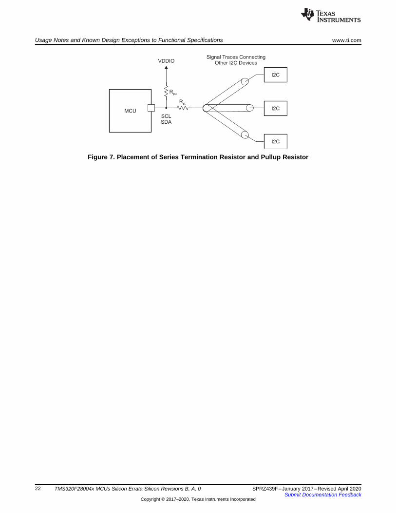
I2C
Signal Traces ConnectingOther I2C DevicesVDDIO
Rpu
Rst
SCLSDA
MCU
I2C
I2C
Usage Notes and Known Design Exceptions to Functional Specifications www.ti.com
22 SPRZ439F–January 2017–Revised April 2020Submit Documentation Feedback
Copyright © 2017–2020, Texas Instruments Incorporated
TMS320F28004x MCUs Silicon Errata Silicon Revisions B, A, 0
Figure 7. Placement of Series Termination Resistor and Pullup Resistor
ePWM Output Pin (Possibility A)
(Trip interrupt will be issued)
ePWM Output Pin (Possibility B)
(Trip interrupt will not be issued)
Active
StateTrip
State
Active
StateTrip
State
Active
StateTrip
State
Active State
Trip ActiveTrip Source
Blanking WindowBlanking Window
Active
Undesired Trip
Active-to-Inactive TransitionTrip Inactive
Blanking Complete
3 ePWM cycles
www.ti.com Usage Notes and Known Design Exceptions to Functional Specifications
23SPRZ439F–January 2017–Revised April 2020Submit Documentation Feedback
Copyright © 2017–2020, Texas Instruments Incorporated
TMS320F28004x MCUs Silicon Errata Silicon Revisions B, A, 0
Advisory ePWM: An ePWM Glitch can Occur if a Trip Remains Active at the End of theBlanking Window
Revision(s) Affected 0, A, B
Details The blanking window is typically used to mask any PWM trip events during transitionswhich would be false trips to the system. If an ePWM trip event remains active for lessthan three ePWM clocks after the end of the blanking window cycles, there can be anundesired glitch at the ePWM output.
Figure 8 illustrates the time period which could result in an undesired ePWM output.
Figure 8. Undesired Trip Event and Blanking Window Expiration
Figure 9 illustrates the two potential ePWM outputs possible if the trip event ends within1 cycle before or 3 cycles after the blanking window closes.
Figure 9. Resulting Undesired ePWM Outputs Possible
Workaround(s) Extend or reduce the blanking window to avoid any undesired trip action.
Usage Notes and Known Design Exceptions to Functional Specifications www.ti.com
24 SPRZ439F–January 2017–Revised April 2020Submit Documentation Feedback
Copyright © 2017–2020, Texas Instruments Incorporated
TMS320F28004x MCUs Silicon Errata Silicon Revisions B, A, 0
Advisory INTOSC: VDDIO Powered Without VDD Can Cause INTOSC Frequency Drift
Revision(s) Affected 0, A, B
Details The "D" revision of the TMS320F28004x Microcontrollers Data Manual (SPRS945D) hasupdated power sequencing requirements. Revision "C" and earlier revisions of the datamanual did not require VDDIO and VDD to be powered on and powered off at the sametime when using an external supply source for VDD.
If VDDIO is powered on while VDD is not powered, there will be an accumulating andpersistent downward frequency drift for INTOSC1 and INTOSC2. The rate of driftaccumulated will be greater when VDDIO is powered without VDD at high temperatures.
As a result of this drift, the INTOSC1 and INTOSC2 internal oscillator frequencies couldfall below the minimum values specified in the data manual. This would impactapplications using INTOSC2 as the clock source for the PLL, with the system operatingat a lower frequency than expected.
Workaround(s)1. Use the internal VREG or internal DCDC, which will ensure VDD is powered when
VDDIO is present.2. When using an external VDD source, always keep VDDIO and VDD powered
together.3. Use the external X1 and X2 crystal oscillators as the PLL clock source. The crystal
oscillator does not have any drift related to VDDIO and VDD supply sequencing.
www.ti.com Usage Notes and Known Design Exceptions to Functional Specifications
25SPRZ439F–January 2017–Revised April 2020Submit Documentation Feedback
Copyright © 2017–2020, Texas Instruments Incorporated
TMS320F28004x MCUs Silicon Errata Silicon Revisions B, A, 0
Advisory FSI: RX FIFO Spurious Overrun
Revision(s) Affected 0, A, B
Details A buffer overrun is asserted when the last location of the FIFO is written.
Workaround(s) Two possible workarounds are available.1. Set up the communication between the transmitting and receiving modules in such a
way that the maximum number of data words received, before the first data word isread, is 15 (not 16). Under this condition, buffer overrun behavior is reliable.
2. If the application must fill all 16 data words in the receive buffer before the first dataword is read (NWORD packet with 16 words), then the following sequence can beused:• Ignore RX buffer overrun RX_EVT_STS.BUF_OVERRUN.• On RX_EVT_STS.FRAME_DONE, read
RX_BUF_PTR_STS.CURR_WORD_CNT and check that it is 16.• Use DMA or software to move the data out of the RX buffer.• Read RX_BUF_PTR_STS.CURR_WORD_CNT and check that it is 0.• Clear the RX_EVT_STS.FRAME_DONE Flag by writing a 1 to
RX_EVT_CLR.FRAME_DONE.
Usage Notes and Known Design Exceptions to Functional Specifications www.ti.com
26 SPRZ439F–January 2017–Revised April 2020Submit Documentation Feedback
Copyright © 2017–2020, Texas Instruments Incorporated
TMS320F28004x MCUs Silicon Errata Silicon Revisions B, A, 0
Advisory During DCAN FIFO Mode, Received Messages May be Placed Out of Order in theFIFO Buffer
Revision(s) Affected 0, A, B
Details In DCAN FIFO mode, received messages with the same arbitration and mask IDs aresupposed to be placed in the FIFO in the order in which they are received. The CPUthen retrieves the received messages from the FIFO via the IF1/IF2 interface registers.Some messages may be placed in the FIFO out of the order in which they werereceived. If the order of the messages is critical to the application for processing, thenthis behavior will prevent the proper use of the DCAN FIFO mode.
Workaround(s) Use the DMA to read out the FIFO via the IF3 register. Each time a message is receivedinto the FIFO, the data is also copied to the IF3 register, and a DMA request Isgenerated to the DMA module to read out the data.
www.ti.com Usage Notes and Known Design Exceptions to Functional Specifications
27SPRZ439F–January 2017–Revised April 2020Submit Documentation Feedback
Copyright © 2017–2020, Texas Instruments Incorporated
TMS320F28004x MCUs Silicon Errata Silicon Revisions B, A, 0
Advisory Boot ROM: Calling SCI Bootloader from Application
Revision(s) Affected 0, A, B
Details The ROM SCI bootloader uses autobaud lock to lock the baud rate. The SCI baud rate issplit between two registers, SCILBAUD and SCIHBAUD. The ROM SCI bootloaderexpects SCIHBAUD to contain its default reset value of zero. If the ROM SCI bootloaderis called from an application that modified the contents of SCIHBAUD to be non-zero,then the SCI will not autobaud-lock and the SCI bootloader will not execute.
Workaround(s) Clear SCIHBAUD to zero before calling the ROM SCI Bootloader.
Usage Notes and Known Design Exceptions to Functional Specifications www.ti.com
28 SPRZ439F–January 2017–Revised April 2020Submit Documentation Feedback
Copyright © 2017–2020, Texas Instruments Incorporated
TMS320F28004x MCUs Silicon Errata Silicon Revisions B, A, 0
Advisory Memory: Prefetching Beyond Valid Memory
Revision(s) Affected 0, A, B
Details The C28x CPU prefetches instructions beyond those currently active in its pipeline. If theprefetch occurs past the end of valid memory, then the CPU may receive an invalidopcode.
Workaround M1, GS3 – The prefetch queue is 8 x16 words in depth. Therefore, code should notcome within 8 words of the end of valid memory. Prefetching across the boundarybetween two valid memory blocks is all right.
Example 1: M1 ends at address 0x7FF and is not followed by another memory block.Code in M1 should be stored no farther than address 0x7F7. Addresses 0x7F8–0x7FFshould not be used for code.
Example 2: M0 ends at address 0x3FF and valid memory (M1) follows it. Code in M0can be stored up to and including address 0x3FF. Code can also cross into M1, up toand including address 0x7F7.
Flash – The prefetch queue is 16 x16 words in depth. Therefore, code should not comewithin 16 words of the end of valid memory; otherwise, it generates a Flash ECCuncorrectable error.
Table 5. Memories Impacted by Advisory
MEMORY TYPE ADDRESSES IMPACTEDM1 0x0000 07F8–0x0000 07FFGS3 0x0001 3FF8–0x0001 3FFFFlash 0x0009 FFF0–0x0009 FFFF
www.ti.com Usage Notes and Known Design Exceptions to Functional Specifications
29SPRZ439F–January 2017–Revised April 2020Submit Documentation Feedback
Copyright © 2017–2020, Texas Instruments Incorporated
TMS320F28004x MCUs Silicon Errata Silicon Revisions B, A, 0
Advisory SYSTEM: Multiple Successive Writes to CLKSRCCTL1 Can Cause a System Hang
Revision(s) Affected 0, A, B
Details When the CLKSRCCTL1 register is written more than once without delay betweenwrites, the system can hang and can only be recovered by an external XRSn reset orWatchdog reset. The occurrence of this condition depends on the clock ratio betweenSYSCLK and the clock selected by OSCCLKSRCSEL, and may not occur every time.
If this issue is encountered while using the debugger, then after hitting pause, theprogram counter will be at the Boot ROM reset vector.
Implementing the workaround will avoid this condition for any SYSCLK to OSCCLK ratio.
Workaround(s) Add a software delay of 300 SYSCLK cycles using an NOP instruction after every writeto the CLKSRCCTL1 register.
Example:
ClkCfgRegs.CLKSRCCTL1.bit.INTOSC2OFF=0; // Turn on INTOSC2asm(" RPT #250 || NOP"); // Delay of 250 SYSCLK Cyclesasm(" RPT #50 || NOP"); // Delay of 50 SYSCLK Cycles
ClkCfgRegs.CLKSRCCTL1.bit.OSCCLKSRCSEL = 0; // Clk Src = INTOSC2asm(" RPT #250 || NOP"); // Delay of 250 SYSCLK Cyclesasm(" RPT #50 || NOP"); // Delay of 50 SYSCLK Cycles
C2000Ware_3_00_00_00 and later revisions will have this workaround implemented.
Usage Notes and Known Design Exceptions to Functional Specifications www.ti.com
30 SPRZ439F–January 2017–Revised April 2020Submit Documentation Feedback
Copyright © 2017–2020, Texas Instruments Incorporated
TMS320F28004x MCUs Silicon Errata Silicon Revisions B, A, 0
Advisory ADC: Interrupts may Stop if INTxCONT (Continue-to-Interrupt Mode) is not Set
Revision(s) Affected 0, A, B
Details If ADCINTSELxNx[INTxCONT] = 0, then interrupts will stop when the ADCINTFLG is setand no additional ADC interrupts will occur.
When an ADC interrupt occurs simultaneously with a software write of theADCINTFLGCLR register, the ADCINTFLG will unexpectedly remain set, blocking futureADC interrupts.
Workaround(s)1. Use Continue-to-Interrupt Mode to prevent the ADCINTFLG from blocking additional
ADC interrupts:
ADCINTSEL1N2[INT1CONT] = 1;ADCINTSEL1N2[INT2CONT] = 1;ADCINTSEL3N4[INT3CONT] = 1;ADCINTSEL3N4[INT4CONT] = 1;
2. Ensure there is always sufficient time to service the ADC ISR and clear theADCINTFLG before the next ADC interrupt occurs to avoid this condition.
3. Check for an overflow condition in the ISR when clearing the ADCINTFLG. CheckADCINTOVF immediately after writing to ADCINTFLGCLR; if it is set, then writeADCINTFLGCLR a second time to ensure the ADCINTFLG is cleared. TheADCINTOVF register will be set, indicating an ADC conversion interrupt was lost.
AdcaRegs.ADCINTFLGCLR.bit.ADCINT1 = 1; //clear INT1 flagif(1 == AdcaRegs.ADCINTOVF.bit.ADCINT1) //ADCINT overflow{
AdcaRegs.ADCINTFLGCLR.bit.ADCINT1 = 1; //clear INT1 again// If the ADCINTOVF condition will be ignored by the application// then clear the flag here by writing 1 to ADCINTOVFCLR.// If there is a ADCINTOVF handling routine, then either insert// that code and clear the ADCINTOVF flag here or do not clear// the ADCINTOVF here so the external routine will detect the// condition.// AdcaRegs.ADCINTOVFCLR.bit.ADCINT1 = 1; // clear OVF}
www.ti.com Usage Notes and Known Design Exceptions to Functional Specifications
31SPRZ439F–January 2017–Revised April 2020Submit Documentation Feedback
Copyright © 2017–2020, Texas Instruments Incorporated
TMS320F28004x MCUs Silicon Errata Silicon Revisions B, A, 0
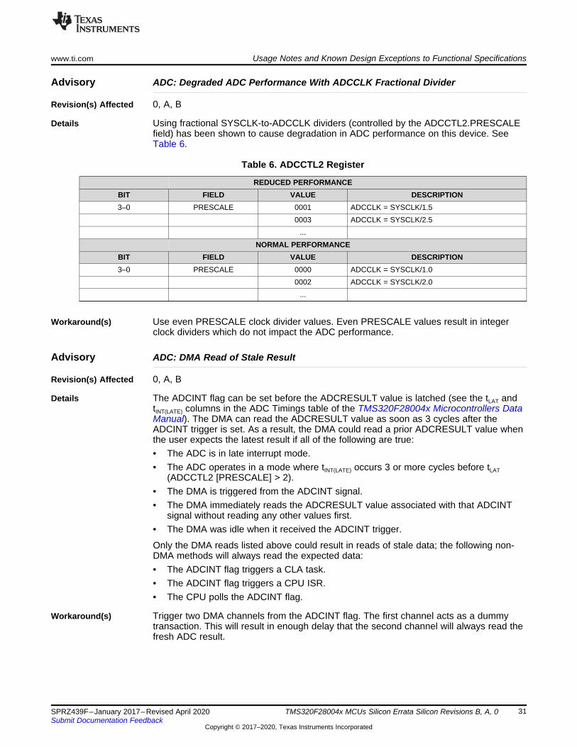
Advisory ADC: Degraded ADC Performance With ADCCLK Fractional Divider
Revision(s) Affected 0, A, B
Details Using fractional SYSCLK-to-ADCCLK dividers (controlled by the ADCCTL2.PRESCALEfield) has been shown to cause degradation in ADC performance on this device. SeeTable 6.
Table 6. ADCCTL2 Register
REDUCED PERFORMANCEBIT FIELD VALUE DESCRIPTION3–0 PRESCALE 0001 ADCCLK = SYSCLK/1.5
0003 ADCCLK = SYSCLK/2.5...
NORMAL PERFORMANCEBIT FIELD VALUE DESCRIPTION3–0 PRESCALE 0000 ADCCLK = SYSCLK/1.0
0002 ADCCLK = SYSCLK/2.0...
Workaround(s) Use even PRESCALE clock divider values. Even PRESCALE values result in integerclock dividers which do not impact the ADC performance.
Advisory ADC: DMA Read of Stale Result
Revision(s) Affected 0, A, B
Details The ADCINT flag can be set before the ADCRESULT value is latched (see the tLAT andtINT(LATE) columns in the ADC Timings table of the TMS320F28004x Microcontrollers DataManual). The DMA can read the ADCRESULT value as soon as 3 cycles after theADCINT trigger is set. As a result, the DMA could read a prior ADCRESULT value whenthe user expects the latest result if all of the following are true:• The ADC is in late interrupt mode.• The ADC operates in a mode where tINT(LATE) occurs 3 or more cycles before tLAT
(ADCCTL2 [PRESCALE] > 2).• The DMA is triggered from the ADCINT signal.• The DMA immediately reads the ADCRESULT value associated with that ADCINT
signal without reading any other values first.• The DMA was idle when it received the ADCINT trigger.
Only the DMA reads listed above could result in reads of stale data; the following non-DMA methods will always read the expected data:• The ADCINT flag triggers a CLA task.• The ADCINT flag triggers a CPU ISR.• The CPU polls the ADCINT flag.
Workaround(s) Trigger two DMA channels from the ADCINT flag. The first channel acts as a dummytransaction. This will result in enough delay that the second channel will always read thefresh ADC result.
Usage Notes and Known Design Exceptions to Functional Specifications www.ti.com
32 SPRZ439F–January 2017–Revised April 2020Submit Documentation Feedback
Copyright © 2017–2020, Texas Instruments Incorporated
TMS320F28004x MCUs Silicon Errata Silicon Revisions B, A, 0
Advisory Analog Subsystem: Software Configuration for Shared Reference Pins
Revision(s) Affected 0, A
Details Smaller pin-count packages of the F28004x device family have combined VREFHI pins.Software configuration bits are provided in the ANAREFPP register to disable all but oneof the ganged references. This allows correct operation of internal reference mode inthese circumstances. On production (TMS) devices, the Boot ROM will write these bits,and no further action will be required from the user. However, on some TMX devices,this write will not occur.
Workaround(s) For TMX devices, the user should do the following writes one time before trying toconfigure the references for internal reference mode:• 100-pin PZ package: The value 0x0002 should be written to ANAREFPP.• 64-pin PM package: The value 0x0003 should be written to ANAREFPP.• 56-pin RSH package: The value 0x0003 should be written to ANAREFPP.

www.ti.com Usage Notes and Known Design Exceptions to Functional Specifications
33SPRZ439F–January 2017–Revised April 2020Submit Documentation Feedback
Copyright © 2017–2020, Texas Instruments Incorporated
TMS320F28004x MCUs Silicon Errata Silicon Revisions B, A, 0
Advisory Analog Trim of Some TMX Devices
Revision(s) Affected 0, A
Details Some TMX samples may not have analog trims programmed. This could degrade theperformance of the ADC, buffered DAC, internal oscillators, PGA, and internal voltageregulator. A value of all zeros in these trim registers will have the following impact.
TRIM REGISTER IMPACT OF TRIM VALUE EQUAL TO ZEROADC offset AdcaRegs.ADCOFFTRIM Degraded performance of the ADC offset error
specification.AdcbRegs.ADCOFFTRIMAdccRegs.ADCOFFTRIM
ADC reference AnalogSubsysRegs.ANAREFTRIMA Degraded performance of the ADC for allspecifications. No workaround available.AnalogSubsysRegs.ANAREFTRIMB
AnalogSubsysRegs.ANAREFTRIMCADC linearity AdcaRegs.ADCINLTRIM2-3 Degraded INL and DNL specifications of the ADC.
No workaround available.AdcbRegs.ADCINLTRIM2-3AdccRegs.ADCINLTRIM2-3
Internal oscillator AnalogSubsysRegs.INTOSC1TRIM Degraded frequency accuracy and temperaturedrift of the internal oscillators.AnalogSubsysRegs.INTOSC2TRIM
Buffered DAC offset DacaRegs.DACTRIM Degraded offset error specification of the bufferedDAC. No workaround available.DacbRegs.DACTRIM
PGA gain and offset PGAGAIN3TRIM Degraded performance of the PGA gain and offseterror specifications. No workaround available.PGAGAIN6TRIM
PGAGAIN12TRIMPGAGAIN24TRIM
Workaround(s) The following workarounds can be used for improved performance, though it still may notmeet data sheet specifications.
Missing ADC offset trim can be generated by following the instructions in the ADC ZeroOffset Calibration section of the TMS320F28004x Microcontrollers Technical ReferenceManual.
If the internal oscillator trim contains all zeros, the user can adjust the lowest 10 bits ofthe oscillator trim register between 1 (minimum) and 1023 (maximum) while observingthe system clock on the XCLOCKOUT pin.
Usage Notes and Known Design Exceptions to Functional Specifications www.ti.com
34 SPRZ439F–January 2017–Revised April 2020Submit Documentation Feedback
Copyright © 2017–2020, Texas Instruments Incorporated
TMS320F28004x MCUs Silicon Errata Silicon Revisions B, A, 0
Advisory PGA: Output Filter Path is Not Supported
Revision(s) Affected 0, A
Details The PGA module includes an embedded series-resistor signal path (RFILTER) forimplementing a low-pass filter at the PGA_OF pin. This RFILTER signal path should not beused or enabled on the affected revisions.
The alternate functions shared with RFILTER on the PGA_OF pin are not affected. Forexample, ADC input signals A2 and B6 are still available on PGA1_OF.
Workaround(s) None
www.ti.com Usage Notes and Known Design Exceptions to Functional Specifications
35SPRZ439F–January 2017–Revised April 2020Submit Documentation Feedback
Copyright © 2017–2020, Texas Instruments Incorporated
TMS320F28004x MCUs Silicon Errata Silicon Revisions B, A, 0
Advisory ROM: Flash API Library and FPU32 Twiddle Factor RFFT Table Not Present
Revision(s) Affected 0, A
Details In the affected revisions, the Flash API library and the FPU32 twiddle factor for the1024-pt RFFT table are not present in the ROM. For details on the ROM contents, seethe Memory Maps section of the ROM Code and Peripheral Booting chapter in theTMS320F28004x Microcontrollers Technical Reference Manual.
Workaround(s) None
Usage Notes and Known Design Exceptions to Functional Specifications www.ti.com
36 SPRZ439F–January 2017–Revised April 2020Submit Documentation Feedback
Copyright © 2017–2020, Texas Instruments Incorporated
TMS320F28004x MCUs Silicon Errata Silicon Revisions B, A, 0
Advisory REVID: Some TMX Revision A Devices Have an Incorrect REVID Value
Revision(s) Affected A
Details Some early TMX Revision A devices have an incorrect value in REVID (address0x0005_D00C). The REVID incorrectly indicates the Revision 0 value (0x0000_0000)instead of the correct Revision A value (0x0000_0001). Software that uses REVID todistinguish between Revision 0 and Revision A will not function as intended. There areno other functional impacts due to this erratum. Applications that do not use REVID insoftware will work properly as any other Revision A device.
Lot Trace Code affected:• 65AVVDW• 66ALSXW
Workaround(s) The device markings on the package are correct and can be used to identify the devicerevision.
www.ti.com Usage Notes and Known Design Exceptions to Functional Specifications
37SPRZ439F–January 2017–Revised April 2020Submit Documentation Feedback
Copyright © 2017–2020, Texas Instruments Incorporated
TMS320F28004x MCUs Silicon Errata Silicon Revisions B, A, 0
Advisory GPIO: X2/GPIO18 Pin Pullup Current During Power Up
Revision(s) Affected 0, A, B
Details During power up, a pullup current of approximately 1.8 mA will be seen on X2/GPIO18.This pin will revert to input mode and operate per the pin description by the time XRSnreleases (transitions to high).
Workaround(s) None
Usage Notes and Known Design Exceptions to Functional Specifications www.ti.com
38 SPRZ439F–January 2017–Revised April 2020Submit Documentation Feedback
Copyright © 2017–2020, Texas Instruments Incorporated
TMS320F28004x MCUs Silicon Errata Silicon Revisions B, A, 0
Advisory GPIO: Open-Drain Configuration May Drive a Short High Pulse
Revision(s) Affected 0, A, B
Details Each GPIO can be configured to an open-drain mode using the GPxODR register.However, an internal device timing issue may cause the GPIO to drive a logic-high for upto 0–10 ns during the transition into or out of the high-impedance state.
This undesired high-level may cause the GPIO to be in contention with another open-drain driver on the line if the other driver is simultaneously driving low. The contention isundesirable because it applies stress to both devices and results in a brief intermediatevoltage level on the signal. This intermediate voltage level may be incorrectly interpretedas a high level if there is not sufficient logic-filtering present in the receiver logic to filterthis brief pulse.
Workaround(s) If contention is a concern, do not use the open-drain functionality of the GPIOs; instead,emulate open-drain mode in software. Open-drain emulation can be achieved by settingthe GPIO data (GPxDAT) to a static 0 and toggling the GPIO direction bit (GPxDIR) toenable and disable the drive low. For an example implementation, see the code below.
void main(void){ ...
// GPIO configurationEALLOW; // disable pullupGpioCtrlRegs.GPxPUD.bit.GPIOx = 1; // disable open-drain modeGpioCtrlRegs.GPxODR.bit.GPIOx = 0; // set GPIO to drive static 0 before
// enabling outputGpioDataRegs.GPxCLEAR.bit.GPIOx = 1;EDIS;
...
// application code...
// To drive 0, set GPIO direction as outputGpioCtrlRegs.GPxDIR.bit.GPIOx = 1;
// To tri-state the GPIO(logic 1),set GPIO as inputGpioCtrlRegs.GPxDIR.bit.GPIOx = 0;
}
www.ti.com Usage Notes and Known Design Exceptions to Functional Specifications
39SPRZ439F–January 2017–Revised April 2020Submit Documentation Feedback
Copyright © 2017–2020, Texas Instruments Incorporated
TMS320F28004x MCUs Silicon Errata Silicon Revisions B, A, 0
Advisory GPIO: Parasitic Path to VSS When Maximum VIH is Exceeded in Input Mode
Revision(s) Affected A
Details If a voltage greater than maximum VIH (VDDIO + 0.3 V) is applied to the GPIO pins listedbelow, an internal parasitic path from the pin to VSS may be turned on. This parasiticcurrent can impact the functional operation of the pin. This is more likely to occur at hightemperature. The parasitic path will be removed when the IO is driven below VIL. Thepath will not reactivate until another overvoltage event occurs.• GPIO16• GPIO17• GPIO24• GPIO25• GPIO26• GPIO27• GPIO35 (TDI)• GPIO37 (TDO)• GPIO40• GPIO41• GPIO42• GPIO43
Pins configured for output-only mode (with no other drivers on the pin) will not see anovervoltage condition at the pin and are not affected by this advisory.
Pins configured in input or bidirectional mode can see an overvoltage condition in threeprimary ways:1. The input is driven by a low-impedance driver that can generate a large overshoot at
the input due to impedance mismatch without compensating termination.2. The input sees large transients from external noise sources that rise above VDDIO +
0.3 V at the pin.3. The input is driven by a device powered by a different voltage regulator. When
receiving voltages from another voltage domain, the system design should alwayskeep voltages below maximum VIH. However, due to the increased possibility of thevoltage being temporarily greater than VDDIO + 0.3 V due to a noise event or if there isimproper supply sequencing, then this advisory will apply.
Workaround(s) If any of the above conditions apply for an input or bidirectional pin, insert a seriesresistor between the signal and the input pin. The series resistor should be placed closeto the input pin.
If the overvoltage is due to overshoot (situations #1 or #2 above), a series resistor of100 Ω or greater should be used.
If the overvoltage might be sustained (situation #3 above), a series resistor of 220 Ω orgreater should be used.
Usage Notes and Known Design Exceptions to Functional Specifications www.ti.com
40 SPRZ439F–January 2017–Revised April 2020Submit Documentation Feedback
Copyright © 2017–2020, Texas Instruments Incorporated
TMS320F28004x MCUs Silicon Errata Silicon Revisions B, A, 0
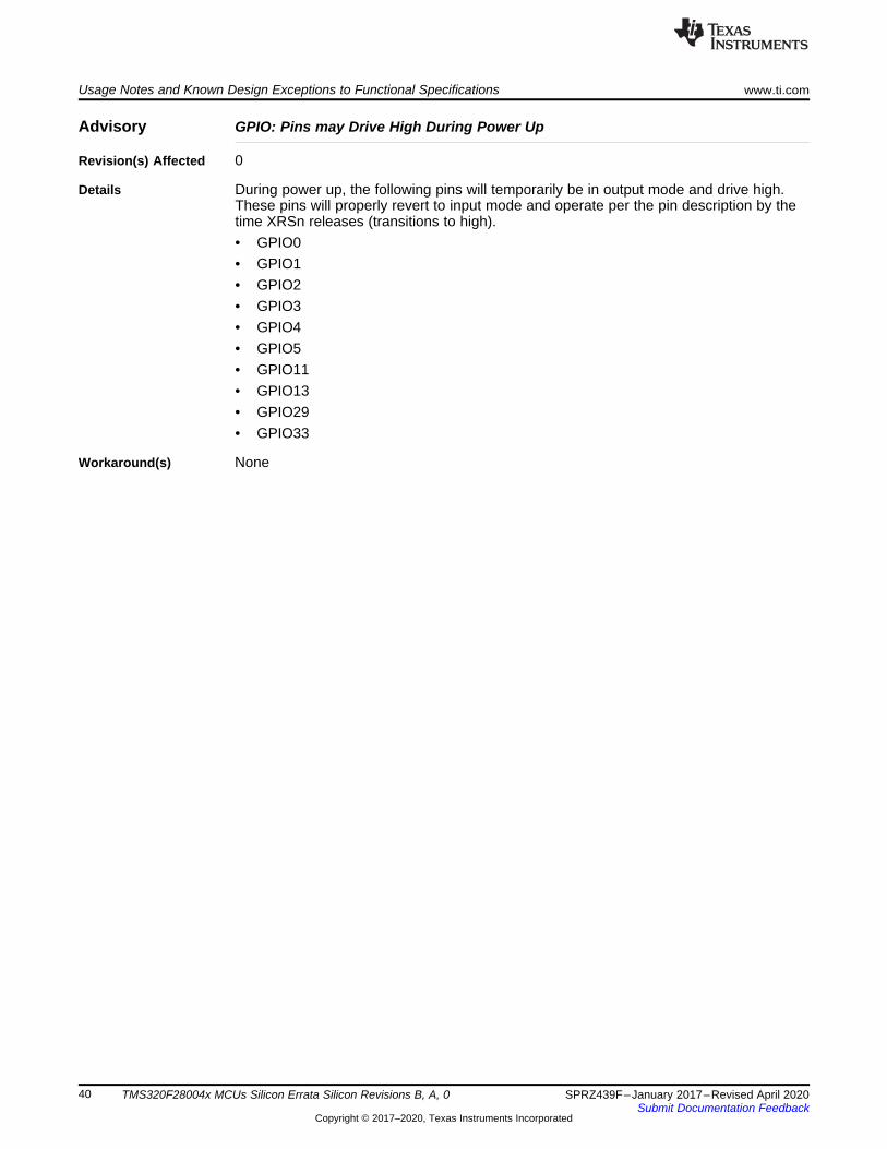
Advisory GPIO: Pins may Drive High During Power Up
Revision(s) Affected 0
Details During power up, the following pins will temporarily be in output mode and drive high.These pins will properly revert to input mode and operate per the pin description by thetime XRSn releases (transitions to high).• GPIO0• GPIO1• GPIO2• GPIO3• GPIO4• GPIO5• GPIO11• GPIO13• GPIO29• GPIO33
Workaround(s) None
www.ti.com Usage Notes and Known Design Exceptions to Functional Specifications
41SPRZ439F–January 2017–Revised April 2020Submit Documentation Feedback
Copyright © 2017–2020, Texas Instruments Incorporated
TMS320F28004x MCUs Silicon Errata Silicon Revisions B, A, 0
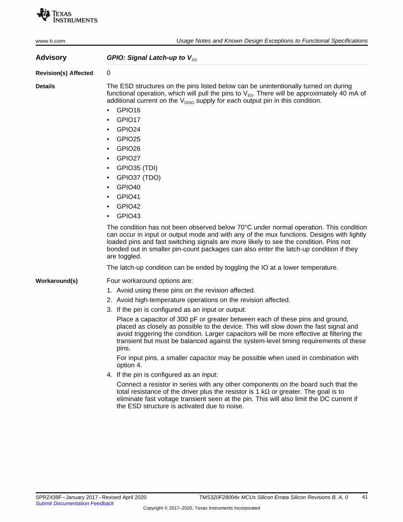
Advisory GPIO: Signal Latch-up to VSS
Revision(s) Affected 0
Details The ESD structures on the pins listed below can be unintentionally turned on duringfunctional operation, which will pull the pins to VSS. There will be approximately 40 mA ofadditional current on the VDDIO supply for each output pin in this condition.• GPIO16• GPIO17• GPIO24• GPIO25• GPIO26• GPIO27• GPIO35 (TDI)• GPIO37 (TDO)• GPIO40• GPIO41• GPIO42• GPIO43
The condition has not been observed below 70°C under normal operation. This conditioncan occur in input or output mode and with any of the mux functions. Designs with lightlyloaded pins and fast switching signals are more likely to see the condition. Pins notbonded out in smaller pin-count packages can also enter the latch-up condition if theyare toggled.
The latch-up condition can be ended by toggling the IO at a lower temperature.
Workaround(s) Four workaround options are:1. Avoid using these pins on the revision affected.2. Avoid high-temperature operations on the revision affected.3. If the pin is configured as an input or output:
Place a capacitor of 300 pF or greater between each of these pins and ground,placed as closely as possible to the device. This will slow down the fast signal andavoid triggering the condition. Larger capacitors will be more effective at filtering thetransient but must be balanced against the system-level timing requirements of thesepins.For input pins, a smaller capacitor may be possible when used in combination withoption 4.
4. If the pin is configured as an input:Connect a resistor in series with any other components on the board such that thetotal resistance of the driver plus the resistor is 1 kΩ or greater. The goal is toeliminate fast voltage transient seen at the pin. This will also limit the DC current ifthe ESD structure is activated due to noise.
Documentation Support www.ti.com
42 SPRZ439F–January 2017–Revised April 2020Submit Documentation Feedback
Copyright © 2017–2020, Texas Instruments Incorporated
TMS320F28004x MCUs Silicon Errata Silicon Revisions B, A, 0
5 Documentation SupportFor more information regarding the F28004x devices, see the following documents:• TMS320F28004x Microcontrollers Data Manual• TMS320F28004x Microcontrollers Technical Reference Manual
www.ti.com Documentation Support
43SPRZ439F–January 2017–Revised April 2020Submit Documentation Feedback
Copyright © 2017–2020, Texas Instruments Incorporated
TMS320F28004x MCUs Silicon Errata Silicon Revisions B, A, 0
TrademarksTMS320 is a trademark of Texas Instruments.All other trademarks are the property of their respective owners.
Revision History www.ti.com
44 SPRZ439F–January 2017–Revised April 2020Submit Documentation Feedback
Copyright © 2017–2020, Texas Instruments Incorporated
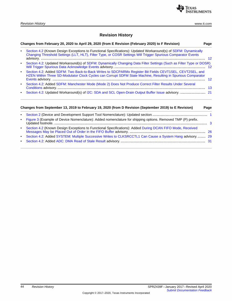
Revision History
Revision History
Changes from February 20, 2020 to April 29, 2020 (from E Revision (February 2020) to F Revision) ....................... Page
• Section 4.2 (Known Design Exceptions to Functional Specifications): Updated Workaround(s) of SDFM: DynamicallyChanging Threshold Settings (LLT, HLT), Filter Type, or COSR Settings Will Trigger Spurious Comparator Eventsadvisory. .................................................................................................................................. 12
• Section 4.2: Updated Workaround(s) of SDFM: Dynamically Changing Data Filter Settings (Such as Filter Type or DOSR)Will Trigger Spurious Data Acknowledge Events advisory. ........................................................................ 12
• Section 4.2: Added SDFM: Two Back-to-Back Writes to SDCPARMx Register Bit Fields CEVT1SEL, CEVT2SEL, andHZEN Within Three SD-Modulator Clock Cycles can Corrupt SDFM State Machine, Resulting in Spurious ComparatorEvents advisory. ......................................................................................................................... 12
• Section 4.2: Added SDFM: Manchester Mode (Mode 2) Does Not Produce Correct Filter Results Under SeveralConditions advisory. ..................................................................................................................... 13
• Section 4.2: Updated Workaround(s) of I2C: SDA and SCL Open-Drain Output Buffer Issue advisory. .................... 21
Changes from September 13, 2019 to February 19, 2020 (from D Revision (September 2019) to E Revision) ......... Page
• Section 2 (Device and Development Support Tool Nomenclature): Updated section. ........................................... 1• Figure 3 (Example of Device Nomenclature): Added nomenclature for shipping options. Removed TMP (P) prefix.
Updated footnote. ......................................................................................................................... 3• Section 4.2 (Known Design Exceptions to Functional Specifications): Added During DCAN FIFO Mode, Received
Messages May be Placed Out of Order in the FIFO Buffer advisory. ............................................................ 26• Section 4.2: Added SYSTEM: Multiple Successive Writes to CLKSRCCTL1 Can Cause a System Hang advisory. ...... 29• Section 4.2: Added ADC: DMA Read of Stale Result advisory. ................................................................... 31

IMPORTANT NOTICE AND DISCLAIMER
TI PROVIDES TECHNICAL AND RELIABILITY DATA (INCLUDING DATASHEETS), DESIGN RESOURCES (INCLUDING REFERENCE DESIGNS), APPLICATION OR OTHER DESIGN ADVICE, WEB TOOLS, SAFETY INFORMATION, AND OTHER RESOURCES “AS IS” AND WITH ALL FAULTS, AND DISCLAIMS ALL WARRANTIES, EXPRESS AND IMPLIED, INCLUDING WITHOUT LIMITATION ANY IMPLIED WARRANTIES OF MERCHANTABILITY, FITNESS FOR A PARTICULAR PURPOSE OR NON-INFRINGEMENT OF THIRD PARTY INTELLECTUAL PROPERTY RIGHTS.These resources are intended for skilled developers designing with TI products. You are solely responsible for (1) selecting the appropriate TI products for your application, (2) designing, validating and testing your application, and (3) ensuring your application meets applicable standards, and any other safety, security, or other requirements. These resources are subject to change without notice. TI grants you permission to use these resources only for development of an application that uses the TI products described in the resource. Other reproduction and display of these resources is prohibited. No license is granted to any other TI intellectual property right or to any third party intellectual property right. TI disclaims responsibility for, and you will fully indemnify TI and its representatives against, any claims, damages, costs, losses, and liabilities arising out of your use of these resources.TI’s products are provided subject to TI’s Terms of Sale (www.ti.com/legal/termsofsale.html) or other applicable terms available either on ti.com or provided in conjunction with such TI products. TI’s provision of these resources does not expand or otherwise alter TI’s applicable warranties or warranty disclaimers for TI products.
Mailing Address: Texas Instruments, Post Office Box 655303, Dallas, Texas 75265Copyright © 2020, Texas Instruments Incorporated