Embed Size (px)
Citation preview
Product
Folder
Sample &Buy
Technical
Documents
Tools &
Software
Support &Community
An IMPORTANT NOTICE at the end of this data sheet addresses availability, warranty, changes, use in safety-critical applications,intellectual property matters and other important disclaimers. PRODUCTION DATA.
TMS3705SCBS881D –JANUARY 2010–REVISED OCTOBER 2016
TMS3705 Transponder Base Station IC
1 Device Overview
1
1.1 Features1
• Base Station IC for TI-RFid™ RF IdentificationSystems
• Drives Antenna• Sends Modulated Data to Antenna• Detects and Demodulates Transponder Response
(FSK)
• Short-Circuit Protection• Diagnosis• Sleep-Mode Supply Current: 0.2 mA• Designed for Automotive Requirements• 16-Pin SOIC (D) Package
1.2 Applications• Car Access• Immobilization
• Building Access• Livestock Reader
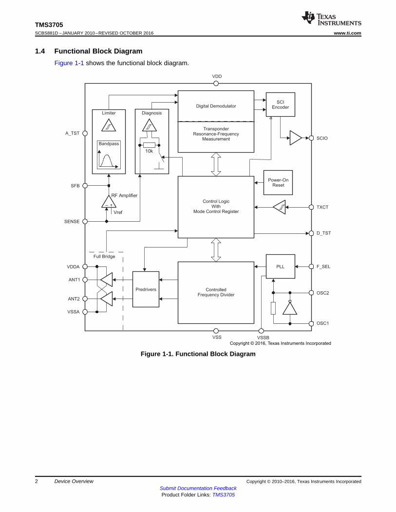
1.3 DescriptionThe TMS3705 transponder base station IC is used to drive the antenna of a TI-RFid transponder system,to send data modulated on the antenna signal, and to detect and demodulate the response of thetransponder. The response of the transponder is a frequency shift keyed (FSK) signal. The high or low bitsare coded in two different high-frequency signals (134.2 kHz for low bits and 123 kHz for high bits,nominal). The transponder induces these signals in the antenna coil according an internally stored code.The energy that the transponder needs to send out the data is stored in a charge capacitor in thetransponder. The antenna field charges this capacitor in a preceding charge phase. The IC has aninterface to an external microcontroller.
There are two configurations for the clock supply to both the microcontroller and the base station IC:1. The microcontroller and base station IC are supplied with a clock signal derived from only one
resonator: The resonator is attached to the microcontroller. The base station IC is supplied with a clocksignal driven by the digital clock output of the microcontroller. The clock frequency is either 4 MHz or2 MHz, depending on the selected microcontroller type.
2. The microcontroller and the base station each have their own resonator.
The base station IC has an on-chip PLL that generates a clock frequency of 16 MHz for internal clocksupply only. Only TMS3705BDRG4 and TMS3705DDRQ1 are recommended in combination with AEStransponder products (for example, TRPWS21GTEA or RF430F5xxx). TMS3705A1DRG4 cannot be usedin combination with AES transponder products.
(1) For the most current part, package, and ordering information for all available devices, see the PackageOption Addendum in Section 9, or see the TI website at www.ti.com.
(2) The sizes shown here are approximations. For the package dimensions with tolerances, see theMechanical Data in Section 9.
Device Information (1)
PART NUMBER PACKAGE BODY SIZE (2)
TMS3705A1DRG4 SOIC (16) 9.9 mm × 3.91 mmTMS3705BDRG4 SOIC (16) 9.9 mm × 3.91 mmTMS3705CDRQ1 SOIC (16) 9.9 mm × 3.91 mmTMS3705DDRQ1 SOIC (16) 9.9 mm × 3.91 mm
Vref
RF Amplifier
10k
A_TST
SFB
SENSE
VDDA
ANT1
ANT2
VSSA
VSS
VDD
SCIO
TXCT
D_TST
F_SEL
OSC2
OSC1
VSSB
Control LogicWith
Mode Control Register
ControlledFrequency Divider
Digital Demodulator
TransponderResonance-Frequency
Measurement
SCIEncoder
Power-OnReset
PLL
Predrivers
Full Bridge
Bandpass
Limiter Diagnosis
Copyright © 2016, Texas Instruments Incorporated
2
TMS3705SCBS881D –JANUARY 2010–REVISED OCTOBER 2016 www.ti.com
Submit Documentation FeedbackProduct Folder Links: TMS3705
Device Overview Copyright © 2010–2016, Texas Instruments Incorporated
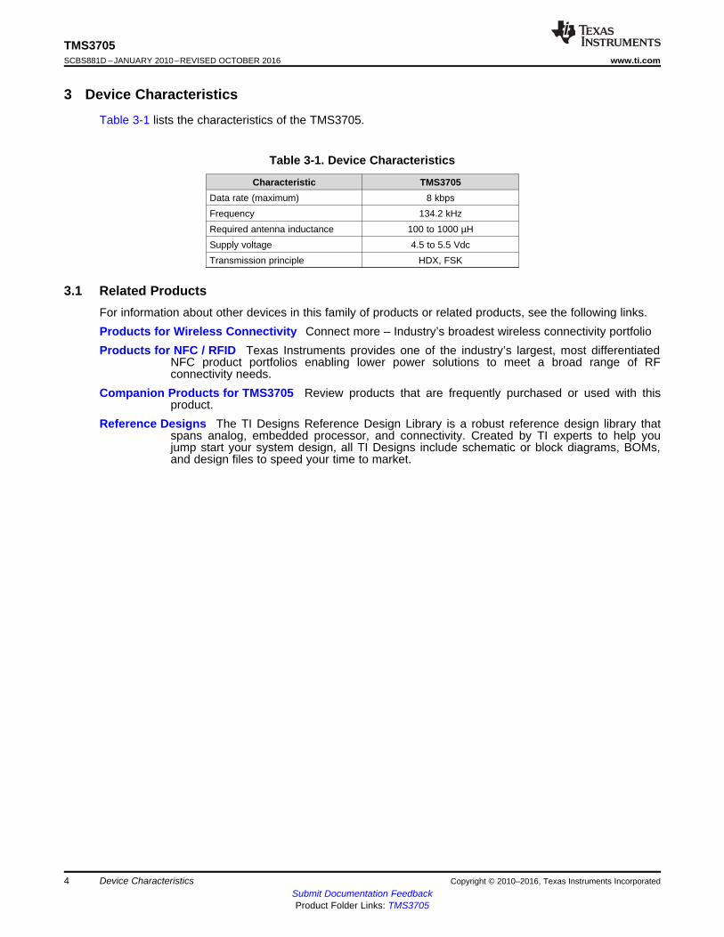
1.4 Functional Block DiagramFigure 1-1 shows the functional block diagram.
Figure 1-1. Functional Block Diagram
3
TMS3705www.ti.com SCBS881D –JANUARY 2010–REVISED OCTOBER 2016
Submit Documentation FeedbackProduct Folder Links: TMS3705
Revision HistoryCopyright © 2010–2016, Texas Instruments Incorporated
Table of Contents1 Device Overview ......................................... 1
1.1 Features .............................................. 11.2 Applications........................................... 11.3 Description............................................ 11.4 Functional Block Diagram ............................ 2
2 Revision History ......................................... 33 Device Characteristics.................................. 4
3.1 Related Products ..................................... 44 Terminal Configuration and Functions.............. 5
4.1 Pin Diagram .......................................... 54.2 Signal Descriptions ................................... 5
5 Specifications ............................................ 65.1 Absolute Maximum Ratings .......................... 65.2 ESD Ratings.......................................... 65.3 Recommended Operating Conditions ................ 65.4 Electrical Characteristics ............................. 75.5 Thermal Resistance Characteristics for D (SOIC)
Package .............................................. 85.6 Switching Characteristics............................. 85.7 Timing Diagrams ..................................... 9
6 Detailed Description ................................... 116.1 Power Supply ....................................... 116.2 Oscillator ............................................ 116.3 Predrivers ........................................... 116.4 Full Bridge........................................... 11
6.5 RF Amplifier ......................................... 116.6 Band-Pass Filter and Limiter........................ 126.7 Diagnosis ............................................ 126.8 Power-on Reset ..................................... 126.9 Frequency Divider................................... 126.10 Digital Demodulator ................................. 126.11 Transponder Resonance-Frequency Measurement 136.12 SCI Encoder......................................... 136.13 Control Logic ........................................ 146.14 Test Pins ............................................ 16
7 Applications, Implementation, and Layout........ 177.1 Application Diagram................................. 17
8 Device and Documentation Support ............... 188.1 Getting Started and Next Steps..................... 188.2 Device Nomenclature ............................... 188.3 Tools and Software ................................. 198.4 Documentation Support ............................. 198.5 Community Resources .............................. 208.6 Trademarks.......................................... 208.7 Electrostatic Discharge Caution..................... 208.8 Export Control Notice ............................... 208.9 Glossary ............................................. 20
9 Mechanical, Packaging, and OrderableInformation .............................................. 21
2 Revision HistoryNOTE: Page numbers for previous revisions may differ from page numbers in the current version.
Changes from April 12, 2016 to October 18, 2016 Page
• Updated the last paragraph in Section 1.3, Description ......................................................................... 1• Added TMS3705CDRQ1 in the Device Information table ....................................................................... 1• Added Section 3, Device Characteristics ......................................................................................... 4• Updated the paragraph that starts "The TMS3705xDRG4 can adjust the carrier frequency..." in Section 6.13,
Control Logic ......................................................................................................................... 16• Added Table 7-1, Bill of Materials (BOM) ....................................................................................... 17• Changed the organization of Section 8, Device and Documentation Support .............................................. 18• Changed Figure 8-1, Device Nomenclature (added silicon rev C and Q100 qualification)................................ 18
4
TMS3705SCBS881D –JANUARY 2010–REVISED OCTOBER 2016 www.ti.com
Submit Documentation FeedbackProduct Folder Links: TMS3705
Device Characteristics Copyright © 2010–2016, Texas Instruments Incorporated
3 Device Characteristics
Table 3-1 lists the characteristics of the TMS3705.
Table 3-1. Device Characteristics
Characteristic TMS3705Data rate (maximum) 8 kbpsFrequency 134.2 kHzRequired antenna inductance 100 to 1000 µHSupply voltage 4.5 to 5.5 VdcTransmission principle HDX, FSK
3.1 Related ProductsFor information about other devices in this family of products or related products, see the following links.Products for Wireless Connectivity Connect more – Industry’s broadest wireless connectivity portfolioProducts for NFC / RFID Texas Instruments provides one of the industry’s largest, most differentiated
NFC product portfolios enabling lower power solutions to meet a broad range of RFconnectivity needs.
Companion Products for TMS3705 Review products that are frequently purchased or used with thisproduct.
Reference Designs The TI Designs Reference Design Library is a robust reference design library thatspans analog, embedded processor, and connectivity. Created by TI experts to help youjump start your system design, all TI Designs include schematic or block diagrams, BOMs,and design files to speed your time to market.
1
2
3
4 13
14
15
16
NC
SCIO
F_SEL
TXCT
A_TST
D_TST
SFB
SENSE
5
6
7 10
11
12
OSC2
OSC1
VSS/VSSB
ANT2
VSSA
ANT1
8 9 VDDVDDA
NC – No connection
5
TMS3705www.ti.com SCBS881D –JANUARY 2010–REVISED OCTOBER 2016
Submit Documentation FeedbackProduct Folder Links: TMS3705
Terminal Configuration and FunctionsCopyright © 2010–2016, Texas Instruments Incorporated
4 Terminal Configuration and Functions
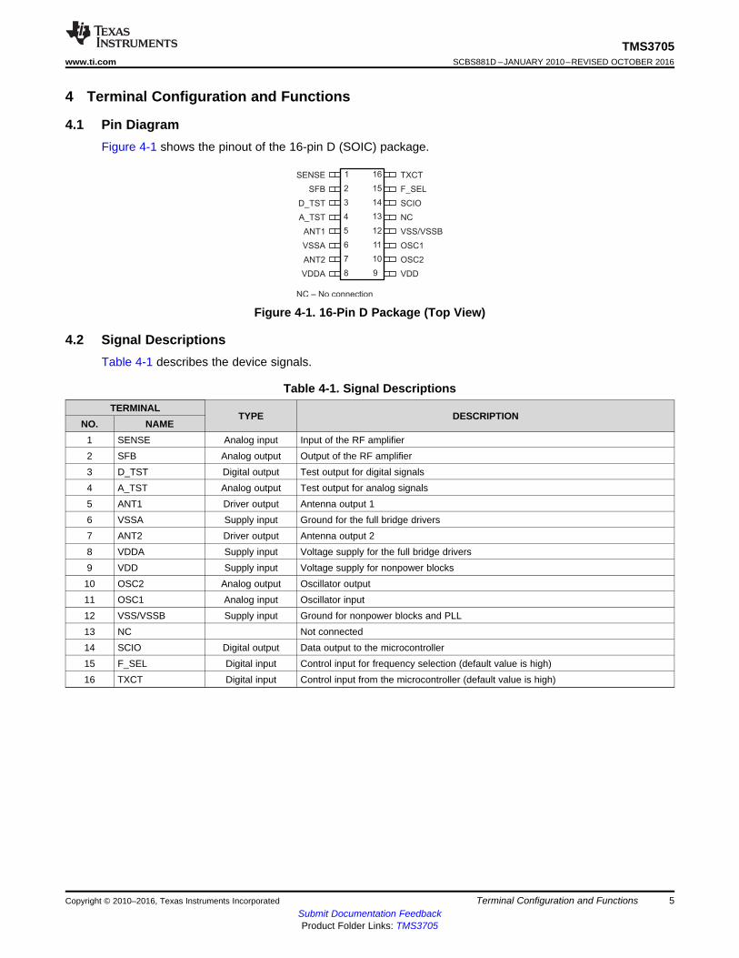
4.1 Pin DiagramFigure 4-1 shows the pinout of the 16-pin D (SOIC) package.
Figure 4-1. 16-Pin D Package (Top View)
4.2 Signal DescriptionsTable 4-1 describes the device signals.
Table 4-1. Signal DescriptionsTERMINAL
TYPE DESCRIPTIONNO. NAME
1 SENSE Analog input Input of the RF amplifier2 SFB Analog output Output of the RF amplifier3 D_TST Digital output Test output for digital signals4 A_TST Analog output Test output for analog signals5 ANT1 Driver output Antenna output 16 VSSA Supply input Ground for the full bridge drivers7 ANT2 Driver output Antenna output 28 VDDA Supply input Voltage supply for the full bridge drivers9 VDD Supply input Voltage supply for nonpower blocks10 OSC2 Analog output Oscillator output11 OSC1 Analog input Oscillator input12 VSS/VSSB Supply input Ground for nonpower blocks and PLL13 NC Not connected14 SCIO Digital output Data output to the microcontroller15 F_SEL Digital input Control input for frequency selection (default value is high)16 TXCT Digital input Control input from the microcontroller (default value is high)
6
TMS3705SCBS881D –JANUARY 2010–REVISED OCTOBER 2016 www.ti.com
Submit Documentation FeedbackProduct Folder Links: TMS3705
Specifications Copyright © 2010–2016, Texas Instruments Incorporated
(1) Stresses beyond those listed under Absolute Maximum Ratings may cause permanent damage to the device. These are stress ratingsonly, and functional operation of the device at these or any other conditions beyond those indicated under Recommended OperatingConditions is not implied. Exposure to absolute-maximum-rated conditions for extended periods may affect device reliability.
5 Specifications
5.1 Absolute Maximum Ratings (1)
over operating free-air temperature range (unless otherwise noted)MIN MAX UNIT
VDD Supply voltage range VDD, VSS/VSSB, VDDA, VSSA –0.3 7 VVOSC Voltage range OSC1, OSC2 –0.3 VDD + 0.3 VVinout Voltage range SCIO, TXCT, F_SEL, D_TST –0.3 VDD + 0.3 VIinout Overload clamping current SCIO, TXCT, F_SEL, D_TST –5 5 mAVANT Output voltage ANT1, ANT2 –0.3 VDD + 0.3 VIANT Output peak current ANT1, ANT2 –1.1 1.1 AVanalog Voltage range SENSE, SFB, A_TST –0.3 VDD + 0.3 VISENSE SENSE input current SENSE, SFB, A_TST –5 5 mAISFB Input current in case of overvoltage SFB –5 5 mATA Operating ambient temperature –40 85 °CTstg Storage temperature –55 150 °CPD Total power dissipation at TA = 85°C 0.5 W
5.2 ESD RatingsVALUE UNIT
VESD ESD protection (MIL STD 883) ±2000 V
5.3 Recommended Operating ConditionsMIN NOM MAX UNIT
VDD Supply voltage VDD, VSS/VSSB, VDDA, VSSA 4.5 5 5.5 Vfosc Oscillator frequency OSC1, OSC2 4 MHzVIH High-level input voltage F_SEL, TXCT, OSC1 0.7 VDD V
VIL Low-level input voltageTXCT, OSC1 0.3 VDD VF_SEL 0.2 VDD
IOH High-level output current SCIO, D_TST –1 mAIOL Low-level output current SCIO, D_TST 1 mA
7
TMS3705www.ti.com SCBS881D –JANUARY 2010–REVISED OCTOBER 2016
Submit Documentation FeedbackProduct Folder Links: TMS3705
SpecificationsCopyright © 2010–2016, Texas Instruments Incorporated
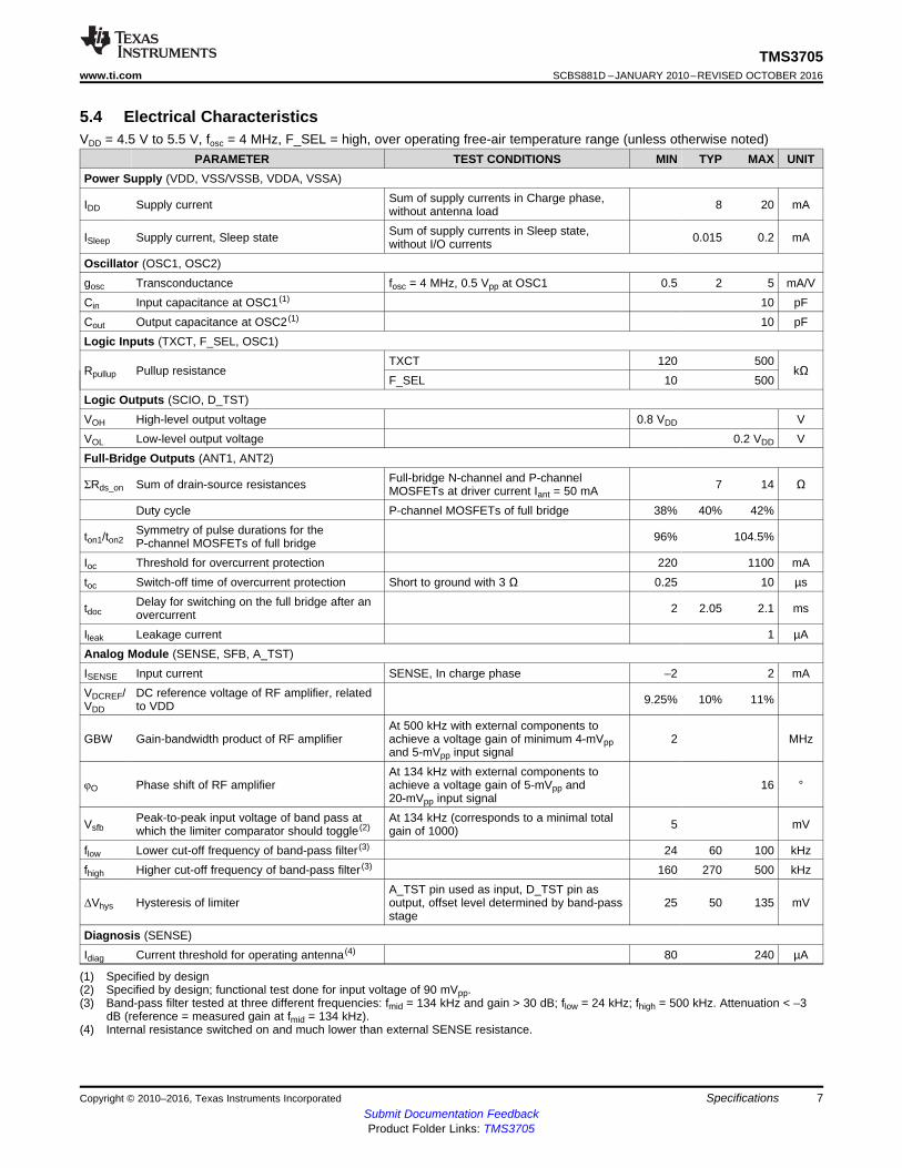
(1) Specified by design(2) Specified by design; functional test done for input voltage of 90 mVpp.(3) Band-pass filter tested at three different frequencies: fmid = 134 kHz and gain > 30 dB; flow = 24 kHz; fhigh = 500 kHz. Attenuation < –3
dB (reference = measured gain at fmid = 134 kHz).(4) Internal resistance switched on and much lower than external SENSE resistance.
5.4 Electrical CharacteristicsVDD = 4.5 V to 5.5 V, fosc = 4 MHz, F_SEL = high, over operating free-air temperature range (unless otherwise noted)
PARAMETER TEST CONDITIONS MIN TYP MAX UNITPower Supply (VDD, VSS/VSSB, VDDA, VSSA)
IDD Supply current Sum of supply currents in Charge phase,without antenna load 8 20 mA
ISleep Supply current, Sleep state Sum of supply currents in Sleep state,without I/O currents 0.015 0.2 mA
Oscillator (OSC1, OSC2)gosc Transconductance fosc = 4 MHz, 0.5 Vpp at OSC1 0.5 2 5 mA/VCin Input capacitance at OSC1 (1) 10 pFCout Output capacitance at OSC2 (1) 10 pFLogic Inputs (TXCT, F_SEL, OSC1)
Rpullup Pullup resistanceTXCT 120 500
kΩF_SEL 10 500
Logic Outputs (SCIO, D_TST)VOH High-level output voltage 0.8 VDD VVOL Low-level output voltage 0.2 VDD VFull-Bridge Outputs (ANT1, ANT2)
ΣRds_on Sum of drain-source resistances Full-bridge N-channel and P-channelMOSFETs at driver current Iant = 50 mA 7 14 Ω
Duty cycle P-channel MOSFETs of full bridge 38% 40% 42%
ton1/ton2Symmetry of pulse durations for theP‑channel MOSFETs of full bridge 96% 104.5%
Ioc Threshold for overcurrent protection 220 1100 mAtoc Switch-off time of overcurrent protection Short to ground with 3 Ω 0.25 10 µs
tdocDelay for switching on the full bridge after anovercurrent 2 2.05 2.1 ms
Ileak Leakage current 1 µAAnalog Module (SENSE, SFB, A_TST)ISENSE Input current SENSE, In charge phase –2 2 mAVDCREF/VDD
DC reference voltage of RF amplifier, relatedto VDD 9.25% 10% 11%
GBW Gain-bandwidth product of RF amplifierAt 500 kHz with external components toachieve a voltage gain of minimum 4‑mVppand 5-mVpp input signal
2 MHz
φO Phase shift of RF amplifierAt 134 kHz with external components toachieve a voltage gain of 5-mVpp and20‑mVpp input signal
16 °
VsfbPeak-to-peak input voltage of band pass atwhich the limiter comparator should toggle (2)
At 134 kHz (corresponds to a minimal totalgain of 1000) 5 mV
flow Lower cut-off frequency of band-pass filter (3) 24 60 100 kHzfhigh Higher cut-off frequency of band-pass filter (3) 160 270 500 kHz
ΔVhys Hysteresis of limiterA_TST pin used as input, D_TST pin asoutput, offset level determined by band-passstage
25 50 135 mV
Diagnosis (SENSE)Idiag Current threshold for operating antenna (4) 80 240 µA
8
TMS3705SCBS881D –JANUARY 2010–REVISED OCTOBER 2016 www.ti.com
Submit Documentation FeedbackProduct Folder Links: TMS3705
Specifications Copyright © 2010–2016, Texas Instruments Incorporated
Electrical Characteristics (continued)VDD = 4.5 V to 5.5 V, fosc = 4 MHz, F_SEL = high, over operating free-air temperature range (unless otherwise noted)
PARAMETER TEST CONDITIONS MIN TYP MAX UNITPhase-Locked Loop (D_TST)fpll PLL frequency 15.984 16 16.0166 MHzΔf/fpll Jitter of the PLL frequency 6%Power-On Reset (POR)Vpor_r POR threshold voltage, rising VDD rising with low slope 1.9 3.5 VVpor_f POR threshold voltage, falling VDD falling with low slope 1.3 2.6 V
(1) The junction-to-ambient thermal resistance under natural convection is obtained in a simulation on a JEDEC-standard, High-K board, asspecified in JESD51-7, in an environment described in JESD51-2a.
5.5 Thermal Resistance Characteristics for D (SOIC) PackagePARAMETER VALUE UNIT
RθJA Thermal resistance, junction to ambient (1) 130 °C/W
5.6 Switching CharacteristicsVDD = 4.5 V to 5.5 V, fosc = 4 MHz, F_SEL = high, over operating free-air temperature range (unless otherwise noted)
PARAMETER TEST CONDITIONS MIN TYP MAX UNIT
tinit minTime for TXCT high to initialize a newtransmission
From start of the oscillator after power onor waking up until reaching the Idle state(see Figure 5-1, Figure 5-2, Figure 5-3)
2 2.05 2.2 ms
tdiagDelay between leaving Idle state and start ofdiagnosis byte at SCIO
Normal operation (see Figure 5-1,Figure 5-2, Figure 5-3) 2 2.12 2.2 ms
tRDelay between end of charge or end ofprogram and start of transponder data transmiton SCIO
See Figure 5-1, Figure 5-2, Figure 5-3. 3 ms
toff Write pulse pause See Figure 5-5. 0.1 ms
tdwriteSignal delay on TXCT for controlling the fullbridge Write mode 73 79 85 µs
tmcr NRZ bit duration for mode control register See Figure 5-4. 121 128 135 µstsci NRZ bit duration on SCIO Asynchronous mode (see Figure 5-6) 63 64 65 µstdstop Low signal delay on TXCT to stop Synchronous mode 128 800 µstt_sync Total TXCT time for reading data on SCIO Synchronous mode (see Figure 5-7) 900 µstsync TXCT period for shifting data on SCIO Synchronous mode (seeFigure 5-7) 4 64 100 µstL_sync Low phase on TXCT Synchronous mode (see Figure 5-7) 2 32 tsync – 2 µstready Data ready for output after SCIO goes high Synchronous mode (see Figure 5-7) 1 127 µs
Startbyte
Diagnosticbyte
tinit tRtch
TXCT
tdiag
Charge Write Response
Data bytes
Phase
SCIO
Initialize transmission
MCW Program
tprog
Startbyte
Diagnosticbyte
tinit tRtch
TXCT
tdiag
Charge Response
Data bytes
Phase
SCIO
Initialize transmission
MCW
Startbyte
Diagnosticbyte
tinit tRtch
TXCT
tdiag
Charge Response
Data bytes
Phase
SCIO
Initialize transmission
MCW
9
TMS3705www.ti.com SCBS881D –JANUARY 2010–REVISED OCTOBER 2016
Submit Documentation FeedbackProduct Folder Links: TMS3705
SpecificationsCopyright © 2010–2016, Texas Instruments Incorporated
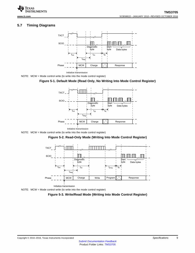
5.7 Timing Diagrams
NOTE: MCW = Mode control write (to write into the mode control register)
Figure 5-1. Default Mode (Read Only, No Writing Into Mode Control Register)
NOTE: MCW = Mode control write (to write into the mode control register)
Figure 5-2. Read-Only Mode (Writing Into Mode Control Register)
NOTE: MCW = Mode control write (to write into the mode control register)
Figure 5-3. Write/Read Mode (Writing Into Mode Control Register)
Stopbit
SCIO
Byteready
tsync
LSB 1 2 3 4 5 6 MSB
TXCT
t ready
Shift data MCU reads data
t L_sync
tsynct t_sync
Stopbit
SCIO
Startbit
tsci
LSB 1 2 3 4 5 6 MSB
tsci
TXCT
Phase Charge High bit Low Program
tch toffHtoffL
tbitH tbitL
t init
TXCT
tmcr
Phase
Initialize transmission
Low
Startbit
Bit1 Bit3 Bit4Bit2
tmcr
Testbit
Charge
End transmission
Bit5 Bit6 Bit7
10
TMS3705SCBS881D –JANUARY 2010–REVISED OCTOBER 2016 www.ti.com
Submit Documentation FeedbackProduct Folder Links: TMS3705
Specifications Copyright © 2010–2016, Texas Instruments Incorporated
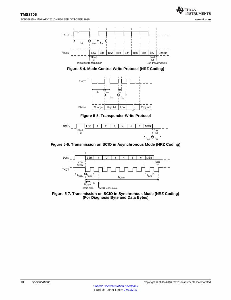
Figure 5-4. Mode Control Write Protocol (NRZ Coding)
Figure 5-5. Transponder Write Protocol
Figure 5-6. Transmission on SCIO in Asynchronous Mode (NRZ Coding)
Figure 5-7. Transmission on SCIO in Synchronous Mode (NRZ Coding)(For Diagnosis Byte and Data Bytes)
11
TMS3705www.ti.com SCBS881D –JANUARY 2010–REVISED OCTOBER 2016
Submit Documentation FeedbackProduct Folder Links: TMS3705
Detailed DescriptionCopyright © 2010–2016, Texas Instruments Incorporated
6 Detailed Description
6.1 Power SupplyThe device is supplied with 5 V by an external voltage regulator through two supply pins, one for providingthe driver current for the antenna and the analog part in front of the digital demodulator and one forsupplying the other blocks.
The power supply supplies a power-on reset that brings the control logic into Idle state as soon as thesupply voltage drops under a certain value.
In Sleep state, the sum of both supply currents is reduced to 0.2 mA. The base station device falls intoSleep state 100 ms after TXCT has changed to high. When TXCT changes to low or is low, the basestation IC immediately goes into and remains in normal operation.
6.2 OscillatorThe oscillator generates the clock of the base station IC of which all timing signals are derived. Betweenits input and output a crystal or ceramic resonator is connected that oscillates at a typical frequency of4 MHz. If a digital clock signal with a frequency of 4 MHz or 2 MHz is supplied to pin OSC1, the signal canbe used to generate the internal operation frequency of 16 MHz.
The oscillator block contains a PLL that generates the internal clock frequency of 16 MHz from the inputclock signal. The PLL multiplies the input clock frequency depending on the logic state of the input pinF_SEL by a factor of 4 (F_SEL is high) or by a factor of 8 (F_SEL is low).
In the Sleep state, the oscillator is off.
6.3 PredriversThe predrivers generate the signals for the four power transistors of the full bridge using the carrierfrequency generated by the frequency divider. The gate signals of the P-channel power transistors (activelow) have the same width (±1 cycle of the 16 MHz clock), the delay between one P-channel MOSFETbeing switched off and the other one being switched on is defined to be 12 cycles of the 16-MHz clock. Inwrite mode the first activation of a gate signal after a bit pause is synchronized to the receivedtransponder signal by a phase shift of 18°.
6.4 Full BridgeThe full bridge drives the antenna current at the carrier frequency during the charge phase and the activetime of the write phase. The minimal load resistance the full bridge sees between its outputs in normaloperation at the resonance frequency of the antenna is 43.3 Ω. When the full bridge is not active, the twodriver outputs are switched to ground.
Both outputs of the full bridge are protected independently against short circuits to ground.
In case of an occurring short circuit, the full bridge is switched off in less than 10 µs to avoid a drop of thesupply voltage. After a delay time of less than 10 ms the full bridge is switched on again to test if the shortcircuit is still there. An overcurrent due to a resistive short to ground that is higher than the maximumcurrent in normal operation but lower than the current threshold for overcurrent protection does not needto be considered.
6.5 RF AmplifierThe RF amplifier is an operational amplifier with a fixed internal voltage reference and a voltage gain of 5defined by external resistors. The RF amplifier has a high gain-bandwidth product of at least 2 MHz toshow a phase shift of less than 16° for the desired signal and to give the possibility to use it as a low-passfilter by adapting additional external components.
The input signal of the RF amplifier is DC coupled to the antenna. The amplitude of the output signal ofthe RF amplifier is higher than 5 mV peak-to-peak.
12
TMS3705SCBS881D –JANUARY 2010–REVISED OCTOBER 2016 www.ti.com
Submit Documentation FeedbackProduct Folder Links: TMS3705
Detailed Description Copyright © 2010–2016, Texas Instruments Incorporated
6.6 Band-Pass Filter and LimiterThe band-pass filter provides amplification and filtering without external components. The lower cut-offfrequency is approximately a factor of 2 lower than the average signal frequency of 130 kHz, the highercut-off frequency is approximately a factor of 2 higher than 130 kHz.
The limiter converts the analog sine-wave signal to a digital signal. The limiter provides a hysteresisdepending on the minimal amplitude of its input signal. The duty cycle of its digital output signal isbetween 40% and 60%. The band-pass filter and the limiter together have a high gain of at least 1000.
6.7 DiagnosisThe diagnosis is carried out during the charge phase to detect whether the full bridge and the antenna areworking. When the full bridge drives the antenna, the voltage across the coil exceeds the supply voltageso that the voltage at the input of the RF amplifier is clamped by the ESD-protection diodes. Fordiagnosis, the SENSE pin is loaded on-chip with a switchable resistor to ground so that the internalswitchable resistor and the external SENSE resistor form a voltage divider, while the internal resistor isswitched off in read mode. When the voltage drop across the internal resistor exceeds a certain value, thediagnosis block passes the frequency of its input signal to the digital demodulator. The frequency of thediagnosis signal is accepted if eight subsequent times can be detected, all with their counter state withinthe range of 112 to 125, during the diagnosis time (at most 0.1 ms). The output signal is used only duringthe charge phase, otherwise it is ignored.
When the short-circuit protection switches off one of the full-bridge drivers, the diagnosis also indicates animproper operation of the antenna by sending the same diagnostic byte to the microcontroller as for theother failure mode.
During diagnosis, the antenna drivers are active. In synchronous mode the antenna drivers remain activeup to 1 ms after the diagnosis is performed, without any respect to the logic state of the signal at TXCT(thus enabling the microcontroller to clock out the diagnosis byte).
6.8 Power-on ResetThe power-on reset generates an internal reset signal to allow the control logic to start up in the definedway.
6.9 Frequency DividerThe frequency divider is a programmable divider that generates the carrier frequency for the full-bridgeantenna drivers. The default value for the division factor is the value 119 needed to provide the nominalcarrier frequency of 134.45 kHz generated from 16 MHz. The resolution for programming the divisionfactor is one divider step that corresponds to a frequency shift of approximately 1.1 kHz. The differentdivision factors needed to cover the range of frequencies for meeting the resonance frequency of thetransponder are 114 to 124.
6.10 Digital DemodulatorThe input signal of the digital demodulator comes from the limiter and is frequency-coded according to thehigh- and low-bit sequence of the transmitted transponder code. The frequency of the input signal ismeasured by counting the oscillation clock for the time period of the input signal. As the high-bit and low-bit frequencies are specified with wide tolerances, the demodulator is designed to distinguish the high-bitand the low-bit frequency by the shift between the two frequencies and not by the absolute values. Thethreshold between the high-bit and the low-bit frequency is defined to be 6.5 kHz lower than the measuredlow-bit frequency and has a hysteresis of ±0.55 kHz.
13
TMS3705www.ti.com SCBS881D –JANUARY 2010–REVISED OCTOBER 2016
Submit Documentation FeedbackProduct Folder Links: TMS3705
Detailed DescriptionCopyright © 2010–2016, Texas Instruments Incorporated
The demodulator is controlled by the control logic. After the charge phase (that is during read or writephase) it measures the time period of its input signal and waits for the transponder resonance-frequencymeasurement to determine the counter state for the threshold between high-bit and low-bit frequency.Then the demodulator waits for the occurrence of the start bit. For that purpose, the results of thecomparisons between the measured time periods and the threshold are shifted in a 12-bit shift register.The detection of the start bit comes into effect when the contents of the shift register matches a specificpattern, indicating 8 subsequent periods below the threshold immediately followed by 4 subsequentperiods above the threshold. A 2-period digital filter is inserted in front of the 12-bit shift register to make astart bit detection possible in case of a nonmonotonous progression of the time periods during a transitionfrom low- to high-bit frequency.
The bit stream detected by the input stage of the digital demodulator passes a digital filter before beingevaluated. After demodulation, the serial bit flow received from the transponder is buffered byte-wisebefore being sent to the microcontroller by SCI encoding.
6.11 Transponder Resonance-Frequency MeasurementDuring the prebit reception phase, the bits the transponder transmits show the low-bit frequency, which isthe resonance frequency of the transponder. The time periods of the prebits are evaluated by thedemodulator counter. Based on the counter states, an algorithm is implemented that ensures a correctmeasurement of the resonance frequency of the transponder:1. A time period of the low-bit frequency has a counter state between 112 and 125.2. The measurement of the low-bit frequency (the average of eight subsequent counter states) is
accepted during the write mode, when the eight time periods have counter states in the defined range.The measurement during write mode is started with the falling edge at TXCT using the fixed delay timeat which end the full bridge is switched on again.
3. The counter state of the measured low-bit frequency results in the average counter state of anaccepted measurement and can be used to update the register of the programmable frequency divider.
4. The measurement of the low-bit frequency (the average of eight subsequent counter states) isaccepted during the read mode, when the eight time periods have counter states in the defined range.The start of the measurement during read mode is delayed to use a stable input signal for themeasurement.
5. The threshold to distinguish between high-bit and low-bit frequency is calculated to be by a value of 5or 7 (see hysteresis in threshold) higher than the counter state of the measured low-bit frequency.
6.12 SCI EncoderAn SCI encoder performs the data transmission to the microcontroller. As the transmission rate of thetransponder is lower than the SCI transmission rate, the serial bit flow received from the transponder isbuffered after demodulation and before SCI encoding.
The SCI encoder uses an 8-bit shift register to send the received data byte-wise (least significant bit first)to the microcontroller with a transmission rate of 15.625 kbaud (±1.5 %), 1 start bit (high), 1 stop bit (low),and no parity bit (asynchronous mode indicated by the SYNC bit of the Mode Control register ispermanently low). The data bits at the SCIO output are inverted with respect to the corresponding bitssent by the transponder.
The transmission starts after the reception of the start bit. The start byte detection is initialized with thefirst rising edge. Typical values for the start byte are 81_H or 01_H (at SCIO). The start byte is the firstbyte to be sent to the microcontroller. The transmission stops and the base station returns to the Idle statewhen TXCT becomes low or 20 ms after the beginning of the read phase. TXCT remains low for at least128 µs to stop the read phase and less than 900 µs to avoid starting the next transmission cycle.
14
TMS3705SCBS881D –JANUARY 2010–REVISED OCTOBER 2016 www.ti.com
Submit Documentation FeedbackProduct Folder Links: TMS3705
Detailed Description Copyright © 2010–2016, Texas Instruments Incorporated
The SCI encoder also sends the diagnostic byte 2 ms after beginning of the charge phase. In case of anormal operation of the antenna, the diagnostic byte AF_H is sent. If no antenna oscillation can bemeasured or if at least one of the full-bridge drivers is switched off due to a detected short circuit, thediagnostic byte FF_H is sent to indicate the failure mode.
The SCI encoder can be switched into a synchronous data transmission mode by setting the mode controlregister bit SYNC to high. In this mode, the output SCIO indicates by a high state that a new byte is readyto be transmitted. The microcontroller can receive the 8 bits at SCIO when sending the eight clock signals(falling edge means active) for the synchronous data transmission through pin TXCT to the SCI encoder.
6.13 Control LogicThe control logic is the core of the TMS3705 circuit. This circuit contains a sequencer or a state machinethat controls the global operations of the base station (see Figure 6-1). This block has a default modeconfiguration but can also be controlled by the microcontroller through the TXCT serial input pin to changethe configuration and to control the programmable frequency divider. For that purpose a mode controlregister is implemented in this module that can be written by the microcontroller.
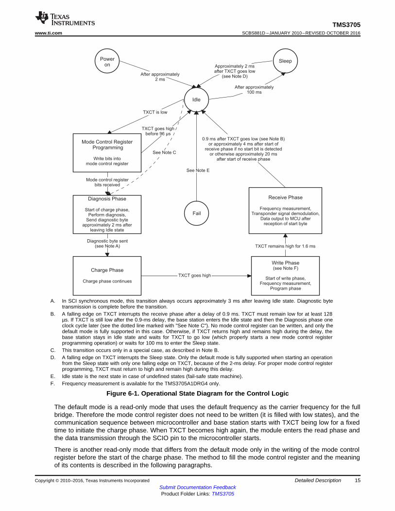
See Note C
Poweron
Sleep
Idle
After approximately2 ms
Approximately 2 msafter TXCT goes low
(see Note D)
TXCT is low
TXCT goes highbefore 96 µs
TXCT goes high
Mode Control RegisterProgramming
Write bits intomode control register
Diagnosis Phase
Start of charge phase,Perform diagnosis,
Send diagnostic byteapproximately 2 ms after
leaving Idle state
Mode control registerbits received
Charge Phase
Charge phase continues
Diagnostic byte sent(see Note A)
Write Phase(see Note F)
Start of write phase,Frequency measurement,
Program phase
Receive Phase
Frequency measurement,Transponder signal demodulation,
Data output to MCU afterreception of start byte
TXCT remains high for 1.6 ms
Fail
See Note E
After approximately100 ms
0.9 ms after TXCT goes low (see Note B)or approximately 4 ms after start of
receive phase if no start bit is detectedor otherwise approximately 20 ms
after start of receive phase
15
TMS3705www.ti.com SCBS881D –JANUARY 2010–REVISED OCTOBER 2016
Submit Documentation FeedbackProduct Folder Links: TMS3705
Detailed DescriptionCopyright © 2010–2016, Texas Instruments Incorporated
A. In SCI synchronous mode, this transition always occurs approximately 3 ms after leaving Idle state. Diagnostic bytetransmission is complete before the transition.
B. A falling edge on TXCT interrupts the receive phase after a delay of 0.9 ms. TXCT must remain low for at least 128µs. If TXCT is still low after the 0.9-ms delay, the base station enters the Idle state and then the Diagnosis phase oneclock cycle later (see the dotted line marked with "See Note C"). No mode control register can be written, and only thedefault mode is fully supported in this case. Otherwise, if TXCT returns high and remains high during the delay, thebase station stays in Idle state and waits for TXCT to go low (which properly starts a new mode control registerprogramming operation) or waits for 100 ms to enter the Sleep state.
C. This transition occurs only in a special case, as described in Note B.D. A falling edge on TXCT interrupts the Sleep state. Only the default mode is fully supported when starting an operation
from the Sleep state with only one falling edge on TXCT, because of the 2-ms delay. For proper mode control registerprogramming, TXCT must return to high and remain high during this delay.
E. Idle state is the next state in case of undefined states (fail-safe state machine).F. Frequency measurement is available for the TMS3705A1DRG4 only.
Figure 6-1. Operational State Diagram for the Control Logic
The default mode is a read-only mode that uses the default frequency as the carrier frequency for the fullbridge. Therefore the mode control register does not need to be written (it is filled with low states), and thecommunication sequence between microcontroller and base station starts with TXCT being low for a fixedtime to initiate the charge phase. When TXCT becomes high again, the module enters the read phase andthe data transmission through the SCIO pin to the microcontroller starts.
There is another read-only mode that differs from the default mode only in the writing of the mode controlregister before the start of the charge phase. The method to fill the mode control register and the meaningof its contents is described in the following paragraphs.
16
TMS3705SCBS881D –JANUARY 2010–REVISED OCTOBER 2016 www.ti.com
Submit Documentation FeedbackProduct Folder Links: TMS3705
Detailed Description Copyright © 2010–2016, Texas Instruments Incorporated
(1) Only available in combination with non-AES transponders
The write-read mode starts with the programming of the mode control register. Then the charge phasestarts with TXCT being low for a fixed time. When TXCT becomes high again, the write phase begins inwhich the data are transmitted from the microcontroller to the transponder through the TXCT pin, thecontrol logic, the predrivers, and the full bridge by amplitude modulation of 100% with a fixed delay time.After the write phase TXCT goes low again to start another charge or program phase. When TXCTbecomes high again, the read phase begins.
The contents of the mode control register (see Table 6-1) define the mode and the way that the carrierfrequency generated by the frequency divider is selected to meet the transponder resonance frequency asclosely as possible.
Table 6-1. Mode Control Register (7-Bit Register)
BIT RESETVALUE DESCRIPTION
NAME NO.START_BIT Bit 0 0 START_BIT = 0 The start bit is always low and does not need to be stored.
DATA_BIT1 Bit 1 0DATA_BIT[4:1] = 0000 Microcontroller selects division factor 119DATA_BIT[4:1] = 1111 Division factor is adapted automatically (1)
DATA_BIT2 Bit 2 0DATA_BIT[4:1] = 0001 Microcontroller selects division factor 114DATA_BIT[4:1] = 0010 Microcontroller selects division factor 115
DATA_BIT3 Bit 3 0... ...DATA_BIT[4:1] = 0110 Microcontroller selects division factor 119
DATA_BIT4 Bit 4 0... ...DATA_BIT[4:1] = 1011 Microcontroller selects division factor 124
SCI_SYNC Bit 5 0SCI_SYNC = 0 Asynchronous data transmission to the microcontrollerSCI_SYNC = 1 Synchronous data transmission to the microcontroller
RX_AFC Bit 6 0RX_AFC = 0 Demodulator threshold is adapted automaticallyRX_AFC = 1 Demodulator threshold is defined by DATA_BIT[4:1]
TEST_BIT Bit 7 0TEST_BIT = 0 No further test bytesTEST_BIT = 1 Further test byte follows for special test modes
The TMS3705xDRG4 can adjust the carrier frequency to the transponder resonance frequencyautomatically by giving the counter state of the transponder resonance-frequency measurement directly tothe frequency divider by setting the first 4 bits in high state. The other combinations of the first 4 bits allowthe microcontroller to select the default carrier frequency or to use another frequency. The division factorcan be selected to be between 114 and 124.
Some bits are included for testability reasons. The default value of these test bits for normal operation islow. Bit 7 (TEST_BIT) is low for normal operation; otherwise, the base station may enter one of the testmodes.
The control logic also controls the demodulator, the SCI encoder, the diagnosis, and the transmission ofthe diagnosis byte during the charge phase.
The state diagram in Figure 6-1 shows the general behavior of the state machine (the state blocks drawncan contain more than one state). All given times are measured from the moment when the state isentered if not specified otherwise.
6.14 Test PinsThe IC has an analog test pin A_TST for the analog part of the receiver. The digital output pin D_TST isused for testing the internal logic. Connecting both pins is not required.
TMS3705
SENSE
SFB
D_TST
A_TST
ANT1
VSSA
ANT2
VDDA VDD
OSC2
OSC1
VSS
NC
SCIO
F_SEL
TXCT
9
10
11
12
13
14
15
16
8
7
6
5
4
3
2
1
C3
C2
Q14 MHzC1
C4
TXCT Input
SCIO Output
5 V
Ground
Antenna
L1
R2
R1
Copyright © 2016, Texas Instruments Incorporated
17
TMS3705www.ti.com SCBS881D –JANUARY 2010–REVISED OCTOBER 2016
Submit Documentation FeedbackProduct Folder Links: TMS3705
Applications, Implementation, and LayoutCopyright © 2010–2016, Texas Instruments Incorporated
7 Applications, Implementation, and Layout
NOTEInformation in the following Applications section is not part of the TI component specification,and TI does not warrant its accuracy or completeness. TI's customers are responsible fordetermining suitability of components for their purposes. Customers should validate and testtheir design implementation to confirm system functionality.
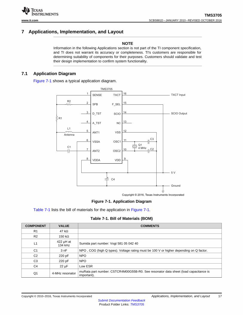
7.1 Application DiagramFigure 7-1 shows a typical application diagram.
Figure 7-1. Application Diagram
Table 7-1 lists the bill of materials for the application in Figure 7-1.
Table 7-1. Bill of Materials (BOM)
COMPONENT VALUE COMMENTSR1 47 kΩR2 150 kΩ
L1 422 µH at134 kHz Sumida part number: Vogt 581 05 042 40
C1 3 nF NPO , COG (high Q types). Voltage rating must be 100 V or higher depending on Q factor.C2 220 pF NPOC3 220 pF NPOC4 22 µF Low ESR
Q1 4-MHz resonator muRata part number: CSTCR4M00G55B-R0. See resonator data sheet (load capacitance isimportant).
Family TMS3705 = Transponder base station IC
Revision A1, B, C, D = Silicon revision
Packaging http://www.ti.com/packaging
Tape and Reel R = Large reel
TMS3705 A
Family
Tape and ReelRevision
Packaging
RD G4
Qualification
QualificationG4 = Green (RoHS and no Sb, Br)Q1 = Q100 Qualified
18
TMS3705SCBS881D –JANUARY 2010–REVISED OCTOBER 2016 www.ti.com
Submit Documentation FeedbackProduct Folder Links: TMS3705
Device and Documentation Support Copyright © 2010–2016, Texas Instruments Incorporated
8 Device and Documentation Support
8.1 Getting Started and Next StepsRFID products from TI provide the ultimate solution for a wide range of applications. With its patentedHDX technology, TI RFID offers unmatched performance in read range, read rate and robustness. Formore information, see Overview for NFC / RFID.
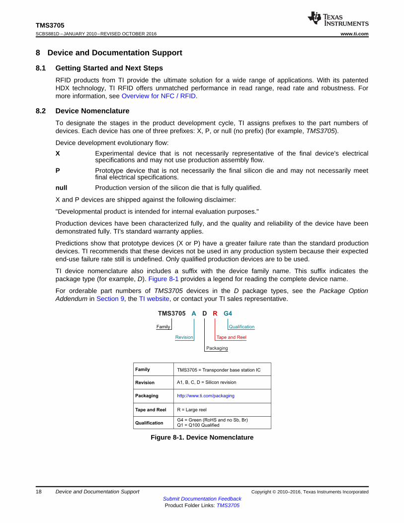
8.2 Device NomenclatureTo designate the stages in the product development cycle, TI assigns prefixes to the part numbers ofdevices. Each device has one of three prefixes: X, P, or null (no prefix) (for example, TMS3705).
Device development evolutionary flow:X Experimental device that is not necessarily representative of the final device's electrical
specifications and may not use production assembly flow.P Prototype device that is not necessarily the final silicon die and may not necessarily meet
final electrical specifications.null Production version of the silicon die that is fully qualified.
X and P devices are shipped against the following disclaimer:
"Developmental product is intended for internal evaluation purposes."
Production devices have been characterized fully, and the quality and reliability of the device have beendemonstrated fully. TI's standard warranty applies.
Predictions show that prototype devices (X or P) have a greater failure rate than the standard productiondevices. TI recommends that these devices not be used in any production system because their expectedend-use failure rate still is undefined. Only qualified production devices are to be used.
TI device nomenclature also includes a suffix with the device family name. This suffix indicates thepackage type (for example, D). Figure 8-1 provides a legend for reading the complete device name.
For orderable part numbers of TMS3705 devices in the D package types, see the Package OptionAddendum in Section 9, the TI website, or contact your TI sales representative.
Figure 8-1. Device Nomenclature
19
TMS3705www.ti.com SCBS881D –JANUARY 2010–REVISED OCTOBER 2016
Submit Documentation FeedbackProduct Folder Links: TMS3705
Device and Documentation SupportCopyright © 2010–2016, Texas Instruments Incorporated
8.3 Tools and SoftwareDesign Kits and Evaluation ModulesLow-Frequency Demo Reader The ADR2 Evaluation Kit contains a low-frequency reader required to
evaluate and operate the TI Car Access products. The kit comes with a reader base board,LF antenna, and a USB-RS232 adapter. Together with the PC software available online, allfunctions of the reader can be controlled and all automotive transponders, remote keylessentry, and passive entry devices can be addressed. Operation of transponder functions andalso passive entry communication is supported by the same system without componentchanges.
PaLFI, Passive Low-Frequency Evaluation Kit TMS37157 The PaLFI Evaluation kit contains allcomponents required to evaluate and operate the TMS37157. The kit comes with an eZ430MSP430F1612 USB development stick, and an MSP430 target board including anMSP430F2274 plus the TMS37157 PaLFI. A battery board for active operation in addition toan RFID base station reader/writer provide the infrastructure for various evaluation setups.
8.4 Documentation SupportThe following documentation describes the transponder, related peripherals, and other technical collateral.
Receiving Notification of Document Updates
To receive notification of documentation updates—including silicon errata—go to the TMS3705 productfolder. In the upper right corner, click the "Alert me" button. This registers you to receive a weekly digest ofproduct information that has changed (if any). For change details, check the revision history of any reviseddocument.
Application ReportsResonant Trimming Sequence This application report presents an efficient and precise method on how
to achieve the desired resonant frequency of configuring the trim array with only a fewiterations and measuring the resonant frequency.
TMS3705 Range Extender Power Solution Using UCC27424-Q1 This application report providessupplementary information about the TI 134.2-kHz RFID Base Station IC TMS3705x incombination with an external driver IC. In particular, the document shows a low cost andeasy-to-implement solution to improve the communication distance between the transactionprocessor (TRP) and the Reader unit.
TMS3705 Passive Antenna Solution The TI low-frequency transponder technology provides thepossibility to use a simple passive antenna in combination with various antenna cablelengths. This solution significantly reduces system costs because the active part of thetransceiver can be added to the already existing host system; for example, the body controlmodule (BCM) of a vehicle.
Integrated TIRIS RF Module TMS3705A Introduction to Low Frequency Reader A TIRIS setupconsists of one or more Transponders and a Reader. The Reader described in thisapplication note normally contains the Reader Antenna, the RF Module and the ControlModule.
More LiteratureWireless Connectivity Tri-fold Overview At TI, we are committed to delivering a broad portfolio of
wireless connectivity solutions which consume the lowest power and are the easiest to use.With TI innovation supporting your designs, you can share, monitor and manage datawirelessly for applications in wearables, home and building automation, manufacturing, smartcities, healthcare and automotive.
MSP430™ Ultra-Low-Power MCUs and TI-RFid Devices The TI portfolio of MSP430 microcontrollersand TI-RFid devices is an ideal fit for low-power, robust RFID reader and transpondersolutions. Together, MSP430 and TI-RFid devices help RF designers achieve low powerconsumption, best-in-class read range and reliable performance at a competitive price.
20
TMS3705SCBS881D –JANUARY 2010–REVISED OCTOBER 2016 www.ti.com
Submit Documentation FeedbackProduct Folder Links: TMS3705
Device and Documentation Support Copyright © 2010–2016, Texas Instruments Incorporated
8.5 Community ResourcesThe following links connect to TI community resources. Linked contents are provided "AS IS" by therespective contributors. They do not constitute TI specifications and do not necessarily reflect TI's views;see TI's Terms of Use.TI E2E™ Online Community The TI engineer-to-engineer (E2E) community was created to foster
collaboration among engineers. At e2e.ti.com, you can ask questions, share knowledge,explore ideas and help solve problems with fellow engineers.
TI Embedded Processors Wiki Established to help developers get started with Embedded Processorsfrom Texas Instruments and to foster innovation and growth of general knowledge about thehardware and software surrounding these devices.
8.6 TrademarksTI-RFid, MSP430, E2E are trademarks of Texas Instruments.All other trademarks are the property of their respective owners.
8.7 Electrostatic Discharge CautionThis integrated circuit can be damaged by ESD. Texas Instruments recommends that all integrated circuits be handled withappropriate precautions. Failure to observe proper handling and installation procedures can cause damage.
ESD damage can range from subtle performance degradation to complete device failure. Precision integrated circuits may be moresusceptible to damage because very small parametric changes could cause the device not to meet its published specifications.
8.8 Export Control NoticeRecipient agrees to not knowingly export or re-export, directly or indirectly, any product or technical data(as defined by the U.S., EU, and other Export Administration Regulations) including software, or anycontrolled product restricted by other applicable national regulations, received from disclosing party undernondisclosure obligations (if any), or any direct product of such technology, to any destination to whichsuch export or re-export is restricted or prohibited by U.S. or other applicable laws, without obtaining priorauthorization from U.S. Department of Commerce and other competent Government authorities to theextent required by those laws.
8.9 GlossaryTI Glossary This glossary lists and explains terms, acronyms, and definitions.
21
TMS3705www.ti.com SCBS881D –JANUARY 2010–REVISED OCTOBER 2016
Submit Documentation FeedbackProduct Folder Links: TMS3705
Mechanical, Packaging, and Orderable InformationCopyright © 2010–2016, Texas Instruments Incorporated
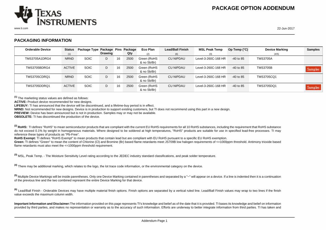
9 Mechanical, Packaging, and Orderable Information
The following pages include mechanical, packaging, and orderable information. This information is themost current data available for the designated devices. This data is subject to change without notice andrevision of this document. For browser-based versions of this data sheet, refer to the left-hand navigation.
PACKAGE OPTION ADDENDUM
www.ti.com 22-Jun-2017
Addendum-Page 1
PACKAGING INFORMATION
Orderable Device Status(1)
Package Type PackageDrawing
Pins PackageQty
Eco Plan(2)
Lead/Ball Finish(6)
MSL Peak Temp(3)
Op Temp (°C) Device Marking(4/5)
Samples
TMS3705A1DRG4 NRND SOIC D 16 2500 Green (RoHS& no Sb/Br)
CU NIPDAU Level-3-260C-168 HR -40 to 85 TMS3705A
TMS3705BDRG4 ACTIVE SOIC D 16 2500 Green (RoHS& no Sb/Br)
CU NIPDAU Level-3-260C-168 HR -40 to 85 TMS3705B
TMS3705CDRQ1 NRND SOIC D 16 2500 Green (RoHS& no Sb/Br)
CU NIPDAU Level-3-260C-168 HR -40 to 85 TMS3705CQ1
TMS3705DDRQ1 ACTIVE SOIC D 16 2500 Green (RoHS& no Sb/Br)
CU NIPDAU Level-3-260C-168 HR -40 to 85 TMS3705DQ1
(1) The marketing status values are defined as follows:ACTIVE: Product device recommended for new designs.LIFEBUY: TI has announced that the device will be discontinued, and a lifetime-buy period is in effect.NRND: Not recommended for new designs. Device is in production to support existing customers, but TI does not recommend using this part in a new design.PREVIEW: Device has been announced but is not in production. Samples may or may not be available.OBSOLETE: TI has discontinued the production of the device.
(2) RoHS: TI defines "RoHS" to mean semiconductor products that are compliant with the current EU RoHS requirements for all 10 RoHS substances, including the requirement that RoHS substancedo not exceed 0.1% by weight in homogeneous materials. Where designed to be soldered at high temperatures, "RoHS" products are suitable for use in specified lead-free processes. TI mayreference these types of products as "Pb-Free".RoHS Exempt: TI defines "RoHS Exempt" to mean products that contain lead but are compliant with EU RoHS pursuant to a specific EU RoHS exemption.Green: TI defines "Green" to mean the content of Chlorine (Cl) and Bromine (Br) based flame retardants meet JS709B low halogen requirements of <=1000ppm threshold. Antimony trioxide basedflame retardants must also meet the <=1000ppm threshold requirement.
(3) MSL, Peak Temp. - The Moisture Sensitivity Level rating according to the JEDEC industry standard classifications, and peak solder temperature.
(4) There may be additional marking, which relates to the logo, the lot trace code information, or the environmental category on the device.
(5) Multiple Device Markings will be inside parentheses. Only one Device Marking contained in parentheses and separated by a "~" will appear on a device. If a line is indented then it is a continuationof the previous line and the two combined represent the entire Device Marking for that device.
(6) Lead/Ball Finish - Orderable Devices may have multiple material finish options. Finish options are separated by a vertical ruled line. Lead/Ball Finish values may wrap to two lines if the finishvalue exceeds the maximum column width.
Important Information and Disclaimer:The information provided on this page represents TI's knowledge and belief as of the date that it is provided. TI bases its knowledge and belief on informationprovided by third parties, and makes no representation or warranty as to the accuracy of such information. Efforts are underway to better integrate information from third parties. TI has taken and
PACKAGE OPTION ADDENDUM
www.ti.com 22-Jun-2017
Addendum-Page 2
continues to take reasonable steps to provide representative and accurate information but may not have conducted destructive testing or chemical analysis on incoming materials and chemicals.TI and TI suppliers consider certain information to be proprietary, and thus CAS numbers and other limited information may not be available for release.
In no event shall TI's liability arising out of such information exceed the total purchase price of the TI part(s) at issue in this document sold by TI to Customer on an annual basis.
TAPE AND REEL INFORMATION
*All dimensions are nominal
Device PackageType
PackageDrawing
Pins SPQ ReelDiameter
(mm)
ReelWidth
W1 (mm)
A0(mm)
B0(mm)
K0(mm)
P1(mm)
W(mm)
Pin1Quadrant
TMS3705A1DRG4 SOIC D 16 2500 330.0 16.4 6.5 10.3 2.1 8.0 16.0 Q1
PACKAGE MATERIALS INFORMATION
www.ti.com 2-Aug-2016
Pack Materials-Page 1
*All dimensions are nominal
Device Package Type Package Drawing Pins SPQ Length (mm) Width (mm) Height (mm)
TMS3705A1DRG4 SOIC D 16 2500 367.0 367.0 38.0
PACKAGE MATERIALS INFORMATION
www.ti.com 2-Aug-2016
Pack Materials-Page 2
IMPORTANT NOTICE
Texas Instruments Incorporated (TI) reserves the right to make corrections, enhancements, improvements and other changes to itssemiconductor products and services per JESD46, latest issue, and to discontinue any product or service per JESD48, latest issue. Buyersshould obtain the latest relevant information before placing orders and should verify that such information is current and complete.TI’s published terms of sale for semiconductor products (http://www.ti.com/sc/docs/stdterms.htm) apply to the sale of packaged integratedcircuit products that TI has qualified and released to market. Additional terms may apply to the use or sale of other types of TI products andservices.Reproduction of significant portions of TI information in TI data sheets is permissible only if reproduction is without alteration and isaccompanied by all associated warranties, conditions, limitations, and notices. TI is not responsible or liable for such reproduceddocumentation. Information of third parties may be subject to additional restrictions. Resale of TI products or services with statementsdifferent from or beyond the parameters stated by TI for that product or service voids all express and any implied warranties for theassociated TI product or service and is an unfair and deceptive business practice. TI is not responsible or liable for any such statements.Buyers and others who are developing systems that incorporate TI products (collectively, “Designers”) understand and agree that Designersremain responsible for using their independent analysis, evaluation and judgment in designing their applications and that Designers havefull and exclusive responsibility to assure the safety of Designers' applications and compliance of their applications (and of all TI productsused in or for Designers’ applications) with all applicable regulations, laws and other applicable requirements. Designer represents that, withrespect to their applications, Designer has all the necessary expertise to create and implement safeguards that (1) anticipate dangerousconsequences of failures, (2) monitor failures and their consequences, and (3) lessen the likelihood of failures that might cause harm andtake appropriate actions. Designer agrees that prior to using or distributing any applications that include TI products, Designer willthoroughly test such applications and the functionality of such TI products as used in such applications.TI’s provision of technical, application or other design advice, quality characterization, reliability data or other services or information,including, but not limited to, reference designs and materials relating to evaluation modules, (collectively, “TI Resources”) are intended toassist designers who are developing applications that incorporate TI products; by downloading, accessing or using TI Resources in anyway, Designer (individually or, if Designer is acting on behalf of a company, Designer’s company) agrees to use any particular TI Resourcesolely for this purpose and subject to the terms of this Notice.TI’s provision of TI Resources does not expand or otherwise alter TI’s applicable published warranties or warranty disclaimers for TIproducts, and no additional obligations or liabilities arise from TI providing such TI Resources. TI reserves the right to make corrections,enhancements, improvements and other changes to its TI Resources. TI has not conducted any testing other than that specificallydescribed in the published documentation for a particular TI Resource.Designer is authorized to use, copy and modify any individual TI Resource only in connection with the development of applications thatinclude the TI product(s) identified in such TI Resource. NO OTHER LICENSE, EXPRESS OR IMPLIED, BY ESTOPPEL OR OTHERWISETO ANY OTHER TI INTELLECTUAL PROPERTY RIGHT, AND NO LICENSE TO ANY TECHNOLOGY OR INTELLECTUAL PROPERTYRIGHT OF TI OR ANY THIRD PARTY IS GRANTED HEREIN, including but not limited to any patent right, copyright, mask work right, orother intellectual property right relating to any combination, machine, or process in which TI products or services are used. Informationregarding or referencing third-party products or services does not constitute a license to use such products or services, or a warranty orendorsement thereof. Use of TI Resources may require a license from a third party under the patents or other intellectual property of thethird party, or a license from TI under the patents or other intellectual property of TI.TI RESOURCES ARE PROVIDED “AS IS” AND WITH ALL FAULTS. TI DISCLAIMS ALL OTHER WARRANTIES ORREPRESENTATIONS, EXPRESS OR IMPLIED, REGARDING RESOURCES OR USE THEREOF, INCLUDING BUT NOT LIMITED TOACCURACY OR COMPLETENESS, TITLE, ANY EPIDEMIC FAILURE WARRANTY AND ANY IMPLIED WARRANTIES OFMERCHANTABILITY, FITNESS FOR A PARTICULAR PURPOSE, AND NON-INFRINGEMENT OF ANY THIRD PARTY INTELLECTUALPROPERTY RIGHTS. TI SHALL NOT BE LIABLE FOR AND SHALL NOT DEFEND OR INDEMNIFY DESIGNER AGAINST ANY CLAIM,INCLUDING BUT NOT LIMITED TO ANY INFRINGEMENT CLAIM THAT RELATES TO OR IS BASED ON ANY COMBINATION OFPRODUCTS EVEN IF DESCRIBED IN TI RESOURCES OR OTHERWISE. IN NO EVENT SHALL TI BE LIABLE FOR ANY ACTUAL,DIRECT, SPECIAL, COLLATERAL, INDIRECT, PUNITIVE, INCIDENTAL, CONSEQUENTIAL OR EXEMPLARY DAMAGES INCONNECTION WITH OR ARISING OUT OF TI RESOURCES OR USE THEREOF, AND REGARDLESS OF WHETHER TI HAS BEENADVISED OF THE POSSIBILITY OF SUCH DAMAGES.Unless TI has explicitly designated an individual product as meeting the requirements of a particular industry standard (e.g., ISO/TS 16949and ISO 26262), TI is not responsible for any failure to meet such industry standard requirements.Where TI specifically promotes products as facilitating functional safety or as compliant with industry functional safety standards, suchproducts are intended to help enable customers to design and create their own applications that meet applicable functional safety standardsand requirements. Using products in an application does not by itself establish any safety features in the application. Designers mustensure compliance with safety-related requirements and standards applicable to their applications. Designer may not use any TI products inlife-critical medical equipment unless authorized officers of the parties have executed a special contract specifically governing such use.Life-critical medical equipment is medical equipment where failure of such equipment would cause serious bodily injury or death (e.g., lifesupport, pacemakers, defibrillators, heart pumps, neurostimulators, and implantables). Such equipment includes, without limitation, allmedical devices identified by the U.S. Food and Drug Administration as Class III devices and equivalent classifications outside the U.S.TI may expressly designate certain products as completing a particular qualification (e.g., Q100, Military Grade, or Enhanced Product).Designers agree that it has the necessary expertise to select the product with the appropriate qualification designation for their applicationsand that proper product selection is at Designers’ own risk. Designers are solely responsible for compliance with all legal and regulatoryrequirements in connection with such selection.Designer will fully indemnify TI and its representatives against any damages, costs, losses, and/or liabilities arising out of Designer’s non-compliance with the terms and provisions of this Notice.
Mailing Address: Texas Instruments, Post Office Box 655303, Dallas, Texas 75265Copyright © 2017, Texas Instruments Incorporated


![TRANSPONDER BYPASS: SENTRY KEY [INSTALLATION GUIDE] · Transponder Bypass: RF override via induction w/ loop antenna (transponder incl. no key required). This transponder bypass kit](https://img.pdfslide.net/doc/110x75/5f51bec37e825f53705baf2b/transponder-bypass-sentry-key-installation-guide-transponder-bypass-rf-override.jpg)