Embed Size (px)
Citation preview
TOC REF GLOSSARY QUIT
Section 3
Component and Assembly Issues
IPC Designer Certification Study Guide
TOC REF GLOSSARY QUIT
Section 3.1
Considerations for Component Mounting
Component and Assembly Issues
TOC REF GLOSSARY QUIT
Considerations for Component Mounting - 3.1
Component mounting and attachment are fast becoming the most important element of printed board design. The issues have always been important because of component density and conductor routing considerations.
TOC REF GLOSSARY QUIT
Considerations for Component Mounting - 3.1
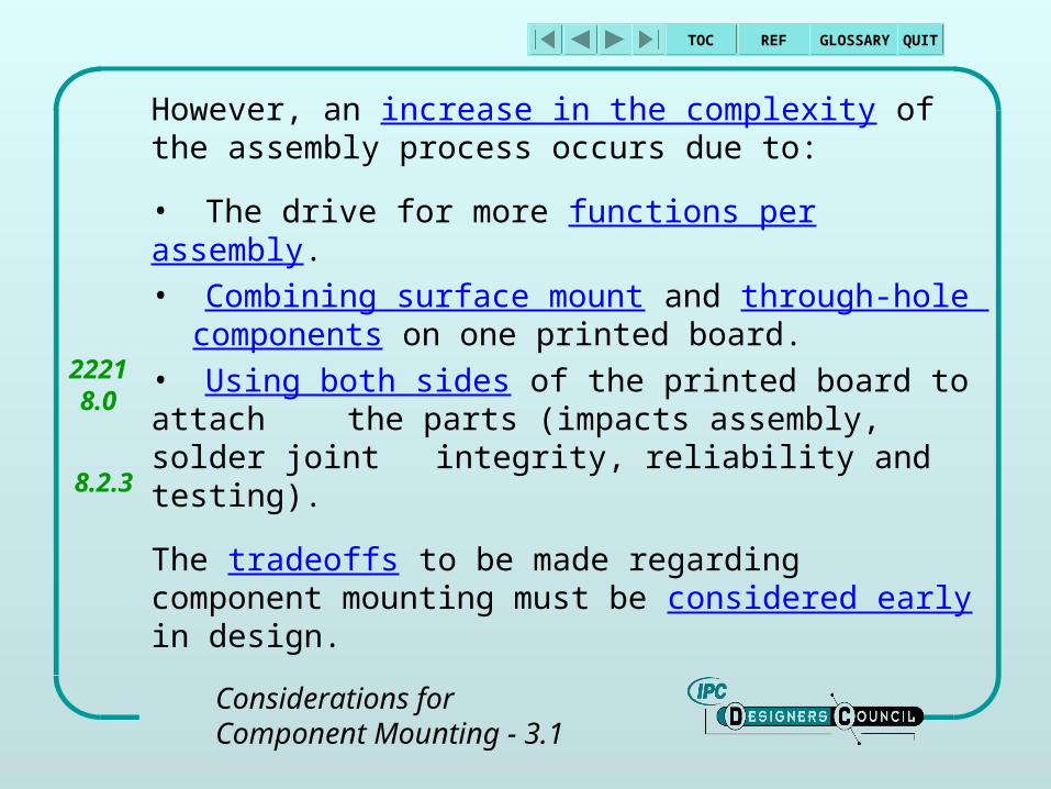
However, an increase in the complexity of the assembly process occurs due to:
• The drive for more functions per assembly.
• Combining surface mount and through-hole components on one printed board.
• Using both sides of the printed board to attach the parts (impacts assembly, solder joint integrity, reliability and testing).
The tradeoffs to be made regarding component mounting must be considered early in design.
22218.0
8.2.3
TOC REF GLOSSARY QUIT
Considerations for Component Mounting - 3.1
Through-hole components are mostly mounted on the side opposite to that which comes into contact with the solder. Automatic insertion techniques are preferred, so rules for these conditions should be taken into account when arranging through-hole parts.
TOC REF GLOSSARY QUIT
Considerations for Component Mounting - 3.1
These rules include appropriate clearances for the insertion heads of the automatic equipment, and having sufficient clearance between the lead diameter and the component hole used for attachment and electrical connection.
The orientation of the components is also important.
TOC REF GLOSSARY QUIT
Considerations for Component Mounting - 3.1
This includes the direction in which the components are lined up electrically with respect to the polarity of polarized components to one another and usually with respect to the board edges.
In addition, uniform component orientation, i.e. all pin #1s located at the lower left, reduces machine cycle time, thus controlling cost during the assembly operation.
22218.1.2
8.1.11
8.2.3
Fig7-1
TOC REF GLOSSARY QUIT
Considerations for Component Mounting - 3.1
The edge of the board becomes the design envelope. Except for connectors, components should not extend over the edge of the board or interfere with board mounting. Design for Assembly (DFA) principles dictate that the designer also know how the assembly will be manufactured.
TOC REF GLOSSARY QUIT
Considerations for Component Mounting - 3.1
Automated techniques require that standard assembly panels be used to maximize the use and the efficiency of the equipment. Special fixtures can accommodate any shape, however, these fixtures add unnecessary cost to the assembly process.
TOC REF GLOSSARY QUIT
Considerations for Component Mounting - 3.1
Thus the board perimeter at LMC (least material condition) should be the boundary that no component, at MMC (maximum material condition), extends beyond. Assembly equipment limitations must be recognized early in the design process. Mounting rails for the automatic machines may require additional clearance. All requirements should be documented on the assembly drawing.
22218.1.5
TOC REF GLOSSARY QUIT
Considerations for Component Mounting - 3.1
There are many other parameters that must be considered for component mounting; component body centering, mounting over conductive areas, clearance between components, and physical support are just a few.
When designing mixed assemblies that include standard SMT parts along with through-hole parts the designer must have close contact with the assembly manufacturing representative to ensure an assembly doesn’t require work-arounds of the process being used by the manufacturer.
TOC REF GLOSSARY QUIT
Considerations for Component Mounting - 3.1
Since many services are provided by the infrastructure of the Electronic Manufacturing Services Industry (EMSI), it is preferred to select the company, or companies, you will work with and tailor the design to their specific process. It should be evident that the design is done once, whereas the board and board assembly are produced many times. Even design changes are easier to implement working with a single or small group of assemblers.
22218.1.7
8.1.10
Fig8-8
TOC REF GLOSSARY QUIT
Considerations for Component Mounting - 3.1
Another element of component mounting that must be considered is the lead clinching requirement.
Is it allowed? Is it required? Sometimes it is left to the discretion of the assembly manufacturer. If the requirements are restrictive they should be indicated on the assembly drawing.
TOC REF GLOSSARY QUIT
Considerations for Component Mounting - 3.1
Some designs require that the dual-inline packages (DIP) have the four corner leads partially bent to a 30 degree angle. This requirement (and any others) for lead clinch should be specified.
TOC REF GLOSSARY QUIT
Considerations for Component Mounting - 3.1
Another element that must be considered is the electrical test considerations. Test point lands must be identified when completing the component placement. In fact, the test strategy should be established before the design starts.
8.3.1.2
8.3.1.3
8.3.1.4
8.3.1.5
Fig8-19
22218.3.1
Fig8-20
TOC REF GLOSSARY QUIT
Section 3.2
Axial and Radial Lead Mounting Differences
Component and Assembly Issues
TOC REF GLOSSARY QUIT
Axial and Radial Lead Mounting Differences - 3.2
Axial leaded components are through-hole components that have the lead wire extending from the component body, or module body, along its longitudinal axis. The leads normally come out in a straight line and must be bent. They enter the holes in the printed board perpendicular to the body of the component.
TOC REF GLOSSARY QUIT
Axial and Radial Lead Mounting Differences - 3.2
The component is horizontally mounted with the component body parallel to the board surface. When bending the leads care must be taken to avoid damaging the seal where the lead connects to the component body.
TOC REF GLOSSARY QUIT
Axial and Radial Lead Mounting Differences - 3.2
When mounting axial leaded parts, the designer should space the holes at a sufficient distance to avoid bending the lead too close to the body of the component. The goal being that the body of the component should be approximately centered between the two mounting holes.
22218.3.1.6
Fig8-21
8.1.6
TOC REF GLOSSARY QUIT
Axial and Radial Lead Mounting Differences - 3.2
The lead extension serves as a form of stress relief and therefore, the tighter the lead is bent to the body of the component the greater stress that can be transferred to the component as the board expands when it heats up in service.
The lead diameter helps to determine where the bend begins. This is usually specified as a minimum of one lead diameter from the component body before the bend radius starts.
TOC REF GLOSSARY QUIT
Axial and Radial Lead Mounting Differences - 3.2
If the component has a weld, or other lead configuration as the lead exits the component, the amount of straight lead distance should be considered after the weld. Although the lead diameter determines the distance prior to bending, that dimension should never be less than 0.75mm [.030"].
22218.1.11
Fig8-9
Fig8-10
TOC REF GLOSSARY QUIT
Axial and Radial Lead Mounting Differences - 3.2
Radial leaded components may have two or more leads exiting from the body. The leads usually come from the same surface and bending may not be necessary as the leads can be inserted directly into the holes of the board. The lead spacing of radial leaded components varies greatly, so the hole spacing is usually predicated by the exit of the leads from the body of the component.
TOC REF GLOSSARY QUIT
Axial and Radial Lead Mounting Differences - 3.2
The DIP is an excellent example of a multiple radial leaded part. The leads of the DIP need not be bent to enter the holes because the part was specifically designed to avoid having to perform the pre-bend operation. However, some small capacitors must have their leads spread slightly in order to have sufficient clearance between the holes.
22218.3.1.7
Fig8-23
Fig8-24
Fig8-25
TOC REF GLOSSARY QUIT
Axial and Radial Lead Mounting Differences - 3.2
Axial or radial leaded parts are intended for through-hole mounting. The axial leaded components are intended to mount horizontally, while the radial leaded parts mount in a vertical axis which is perpendicular to the board.
TOC REF GLOSSARY QUIT
Axial and Radial Lead Mounting Differences - 3.2
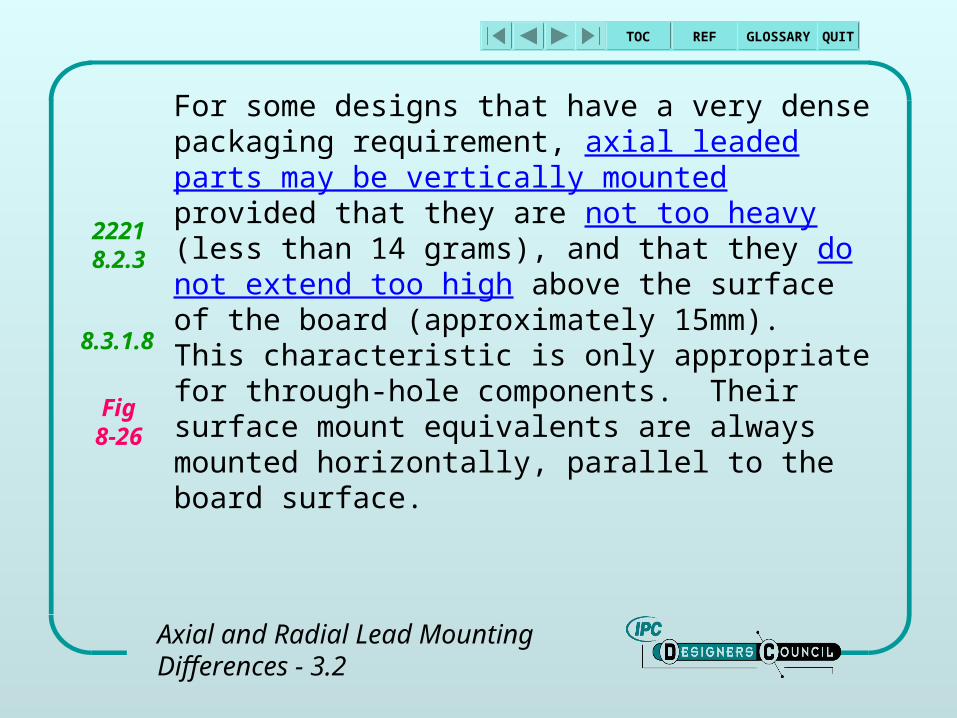
For some designs that have a very dense packaging requirement, axial leaded parts may be vertically mounted provided that they are not too heavy (less than 14 grams), and that they do not extend too high above the surface of the board (approximately 15mm). This characteristic is only appropriate for through-hole components. Their surface mount equivalents are always mounted horizontally, parallel to the board surface.
22218.2.3
8.3.1.8
Fig8-26
TOC REF GLOSSARY QUIT
Axial and Radial Lead Mounting Differences - 3.2
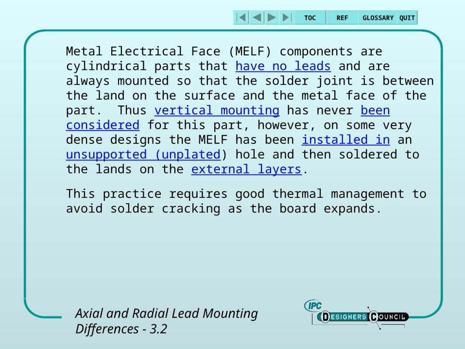
Metal Electrical Face (MELF) components are cylindrical parts that have no leads and are always mounted so that the solder joint is between the land on the surface and the metal face of the part. Thus vertical mounting has never been considered for this part, however, on some very dense designs the MELF has been installed in an unsupported (unplated) hole and then soldered to the lands on the external layers.
This practice requires good thermal management to avoid solder cracking as the board expands.
TOC REF GLOSSARY QUIT
As intermixing components continue to prevail, innovations in the design process become necessary in order to package all the components and circuitry within the design envelope. Through-hole components are modified for surface mounting; surface mount leaded parts are modified for through-hole mounting.
22218.2.3
Axial and Radial Lead Mounting Differences - 3.2
TOC REF GLOSSARY QUIT
Section 3.3
Design Differences for SMT vs. Through-Hole
Component and Assembly Issues
TOC REF GLOSSARY QUIT
Surface mounting is the term given to the method of electrical connection of components to the surface of the conductive pattern.
Surface Mount Technology (SMT) does not utilize component holes.
Design Differences for SMT vs. Through-Hole - 3.3
TOC REF GLOSSARY QUIT
The technique is not new. In the 1960s it was called planar mounting. It came into vogue when ceramic flat pack components were introduced which were hot-bar soldered to the surface of the printed board at a time when most designs used through-hole leaded components.
22218.1.1.3
8.3.1.9
Fig8-27
Fig8-28
Design Differences for SMT vs. Through-Hole - 3.3
TOC REF GLOSSARY QUIT
Design Differences for SMT vs. Through-Hole - 3.3
The industry quickly learned to deal with intermixing of components that mounted to the surface, and those that had to be inserted in plated-though, or unsupported holes. Because the goal has always been to reduce the complexity of the manufacturing and assembly processes, many designers took components that were intended for one or the other technique and modified the leads to accommodate the majority of the components on the board.
TOC REF GLOSSARY QUIT
Design Differences for SMT vs. Through-Hole - 3.3
Through-hole components had their leads flattened, coined, or bent, so that they could be surface mounted. And surface mount parts had leads configured so that they could be inserted into holes. Lead temper and lead length being the major consideration for that approach.
22218.4.4
Fig8-33
TOC REF GLOSSARY QUIT
Design Differences for SMT vs. Through-Hole - 3.3
The industry, then and today, still mounts through-hole axial, radial, and multiple leaded components. When determining the spacing of the lead bends, several considerations are taken into account. These include the distance from the body of the part the leads can be bent, the lead stiffness, the lead diameter (used to determine the bend radius) and the grid system used for the board to locate as many holes as possible on the selected grid.
22218.1.1.2
8.1.11
8.2.1
8.3.1.9
Fig8-27
Fig8-28
TOC REF GLOSSARY QUIT
Design Differences for SMT vs. Through-Hole - 3.3
Intermixing SMT and THT components will be used within the industry for many years. The design for manufacturing issues encourage the designer to work closely with the assembly process engineers in order to achieve the best through-put of the assembly operation. The boards are normally assembled in a panel format, and require careful consideration as to how the parts are positioned, oriented, and arranged, in order to speed-up the assembly operation.
22218.1.1.28.1.118.2.1
8.3.1.9
Fig8-27
Fig8-28
TOC REF GLOSSARY QUIT
Design Differences for SMT vs. Through-Hole - 3.3
The clearances around the parts are determined by the maintenance required. The heads of the insertion or pick and place equipment play a major role in that the designer normally leaves room to provide sufficient clearance for the clinching mechanisms; however, the assembly sequence varies from manufacturer to manufacturer, so the emphasis is usually placed on how difficult it is to replace a faulty component.
TOC REF GLOSSARY QUIT
Design Differences for SMT vs. Through-Hole - 3.3
With that parameter taken into consideration there is usually sufficient clearance for the component placement equipment. Some companies provide this clearance as a standard around the body and land pattern of each component, however, there is no general consensus on what the clearance should be. Much depends on the density of the design and whether the component is repairable or disposable.
22218.2.1
TOC REF GLOSSARY QUIT
Section 3.4
Differences Between Automatic & Manual Insertion
Component and Assembly Issues
TOC REF GLOSSARY QUIT
Differences Between Automatic & Manual Insertion - 3.4
There are many things that must be taken into account when determining the method of through-hole insertion. Manual insertion techniques, although they have greater flexibility for placing components very densely or close together, can be error prone. To reduce the possibility of placing a part in the wrong location has necessitated a great variety of manufacturing assembly aids.
TOC REF GLOSSARY QUIT
Differences Between Automatic & Manual Insertion - 3.4
These aids or systems help to conveyorize the process so that each operator on an assembly line has only a few functions to manage. Components are kitted into groups which, when kept to a minimum number of different or similar parts, are easy to manage.
TOC REF GLOSSARY QUIT
Differences Between Automatic & Manual Insertion - 3.4
Automatic component insertion is the act or operation of assembling discrete components to the printed board by means of electronically controlled equipment. The orientation of the components, the clearance between components, the sequence in which the parts are to be assembled, plus many more factors all become issues that the designer must address.
TOC REF GLOSSARY QUIT
Differences Between Automatic & Manual Insertion - 3.4
The size of the board is also important since many assembly companies want to treat the boards in a panel format to ease board handling. The relationship between the board fabrication panel and the assembly panel, plus the amount of room needed for tooling, or conveyor guides, are issues that impact the design methodology and approval of the final layout.
22218.1.1
8.1.1.3
TOC REF GLOSSARY QUIT
Differences Between Automatic & Manual Insertion - 3.4
The days when printed boards consisted only of through-hole parts are past. Today’s designs have intermixed assemblies that mount both through-hole and surface mount parts. The parts that were only on one side of the board are now on both sides, thus the design process establishing parameters for component positioning must take into account the placement, insertion, and attachment processes used to develop the final assembly.
TOC REF GLOSSARY QUIT
Differences Between Automatic & Manual Insertion - 3.4
Some design facilities pause after initial component placement in the CAD system to send a preliminary arrangement to the assembly company, thus creating a true concurrent engineering environment.
TOC REF GLOSSARY QUIT
Differences Between Automatic & Manual Insertion - 3.4
Lead clinching is another important consideration to be taken into account when deciding if a part is to be manually or automatically inserted. Most automatic equipment heads have the feature capability to clinch leads. They are trimmed to size and then swaged, clinched, or partially clinched to retain the parts during the solder operation.
TOC REF GLOSSARY QUIT
Differences Between Automatic & Manual Insertion - 3.4
It becomes an important parameter for the designer to understand the exact methods for part retention in that the land size or electrical clearance of adjacent conductors can be affected. Manual assembly is less precise and requirements of the design should not exceed the physical dexterity of the operator.
22218.2.1
8.2.2
8.3.1.2
8.3.1.4
Fig7-1
Fig8-19
TOC REF GLOSSARY QUIT
Differences Between Automatic & Manual Insertion - 3.4
Last, but not least, is the relationship between the hole size and the lead diameter. In general, automated assembly requires a slightly larger hole than manual techniques. The larger hole is intended to account for the differences in machine accuracy versus printed board hole location accuracy.
TOC REF GLOSSARY QUIT
Differences Between Automatic & Manual Insertion - 3.4
Some companies provide additional targets called fiducials to compensate for hole to machine location mismatch. Other systems require that the hole is oversize from what it could be with manual insertion. But, it is important that the hole diameter should not exceed the lead diameter too much. If this occurs the solder might not stay in the plated-through, or unsupported hole.
The maximum for automated attachment is usually 0.7mm [.028"] larger than the lead.
22218.3.1
22229.2.2
Fig9-3
TOC REF GLOSSARY QUIT
Section 3.5
Manual vs. Pick-and-Place SMT Placement
Component and Assembly Issues
TOC REF GLOSSARY QUIT
Manual vs. Pick-and-Place SMT Placement - 3.5
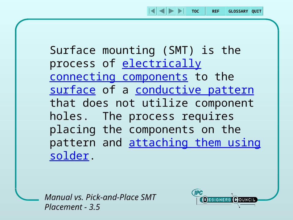
Surface mounting (SMT) is the process of electrically connecting components to the surface of a conductive pattern that does not utilize component holes. The process requires placing the components on the pattern and attaching them using solder.
TOC REF GLOSSARY QUIT
Manual vs. Pick-and-Place SMT Placement - 3.5
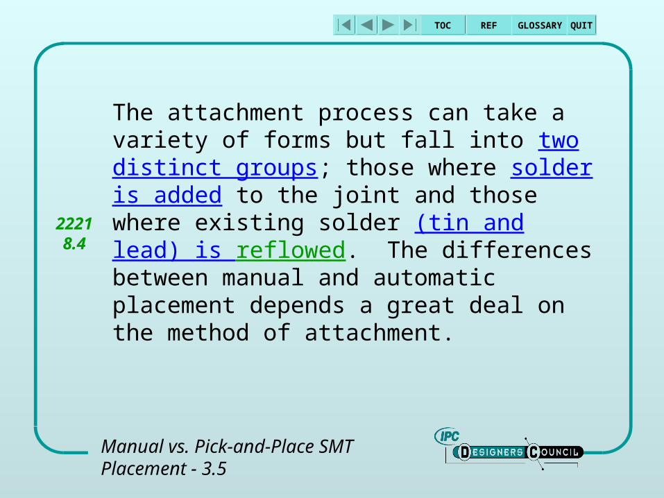
The attachment process can take a variety of forms but fall into two distinct groups; those where solder is added to the joint and those where existing solder (tin and lead) is reflowed. The differences between manual and automatic placement depends a great deal on the method of attachment.
22218.4
TOC REF GLOSSARY QUIT
Manual vs. Pick-and-Place SMT Placement - 3.5
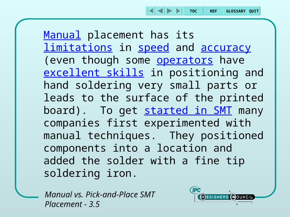
Manual placement has its limitations in speed and accuracy (even though some operators have excellent skills in positioning and hand soldering very small parts or leads to the surface of the printed board). To get started in SMT many companies first experimented with manual techniques. They positioned components into a location and added the solder with a fine tip soldering iron.
TOC REF GLOSSARY QUIT
Manual vs. Pick-and-Place SMT Placement - 3.5
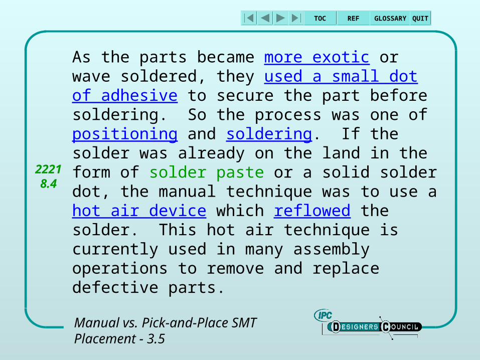
As the parts became more exotic or wave soldered, they used a small dot of adhesive to secure the part before soldering. So the process was one of positioning and soldering. If the solder was already on the land in the form of solder paste or a solid solder dot, the manual technique was to use a hot air device which reflowed the solder. This hot air technique is currently used in many assembly operations to remove and replace defective parts.
22218.4
TOC REF GLOSSARY QUIT
Manual vs. Pick-and-Place SMT Placement - 3.5
It is important to know the methods of attachment in order to take full advantage of the placement technology. Adding solder is done manually with solder paste dispensers (solder dot), or solder wire that contains the flux. Solder is added automatically by:•Sending the board through a wave solder machinewhere a rotating solder wave or dual waves comes into contact with the components and the board. Extra1.11b
TOC REF GLOSSARY QUIT
Manual vs. Pick-and-Place SMT Placement - 3.5
•Drag solderingwhere the parts are brought into contact with a stagnant pool of hot solder.
•Reflow solderingwhich requires that solder is on the land prior to component placement, and that following component placement, the board must be exposed to a heat source in order to get the solder to liquefy or reflow. Techniques include hot air, vapor phase, infra-red, or a combination of these. The reflow may be accomplished in a normal environment or inert environment where a blanket of nitrogen gas improves the reflow process.
TOC REF GLOSSARY QUIT
Manual vs. Pick-and-Place SMT Placement - 3.5
Automatic component placement is performed by machines that pick up parts from reels of tape, trays, or cassettes, hence the name pick-and-place. The placement is very fast and in most instances, very accurate provided that the board or panel is properly registered to the machine origin.
TOC REF GLOSSARY QUIT
Manual vs. Pick-and-Place SMT Placement - 3.5
The fastest machines are those that place discrete resistors and capacitors. These are called “chip shooters.” They place the parts into solder paste that is already on the board, or glue them on the side intended to go through the wave.
Extra1.12c
TOC REF GLOSSARY QUIT
Manual vs. Pick-and-Place SMT Placement - 3.5
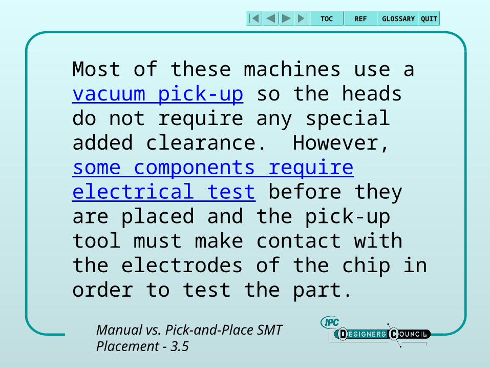
Most of these machines use a vacuum pick-up so the heads do not require any special added clearance. However, some components require electrical test before they are placed and the pick-up tool must make contact with the electrodes of the chip in order to test the part.
TOC REF GLOSSARY QUIT
Manual vs. Pick-and-Place SMT Placement - 3.5
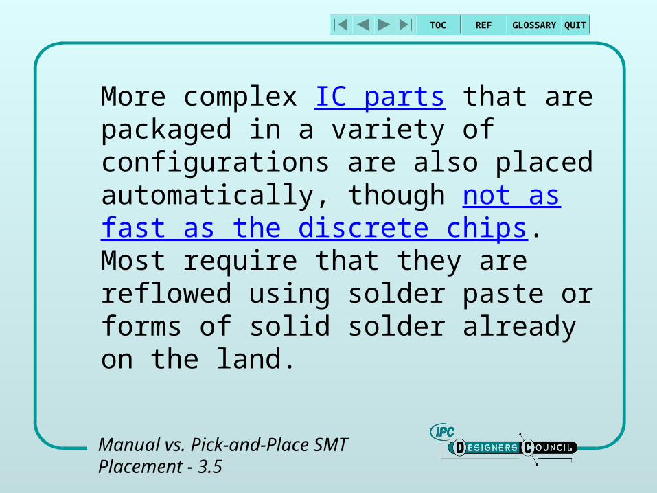
More complex IC parts that are packaged in a variety of configurations are also placed automatically, though not as fast as the discrete chips. Most require that they are reflowed using solder paste or forms of solid solder already on the land.
TOC REF GLOSSARY QUIT
Manual vs. Pick-and-Place SMT Placement - 3.5
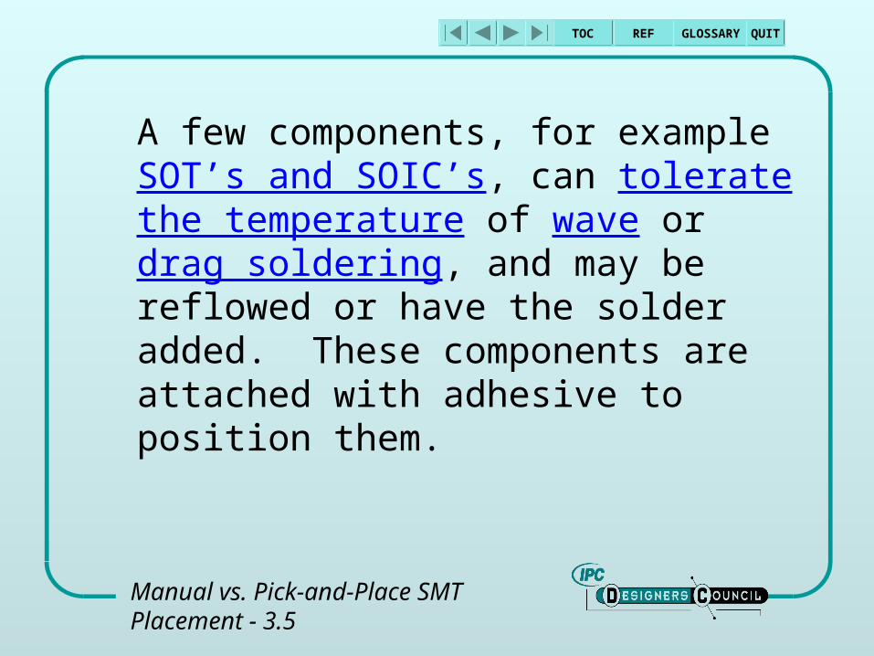
A few components, for example SOT’s and SOIC’s, can tolerate the temperature of wave or drag soldering, and may be reflowed or have the solder added. These components are attached with adhesive to position them.
TOC REF GLOSSARY QUIT
Manual vs. Pick-and-Place SMT Placement - 3.5
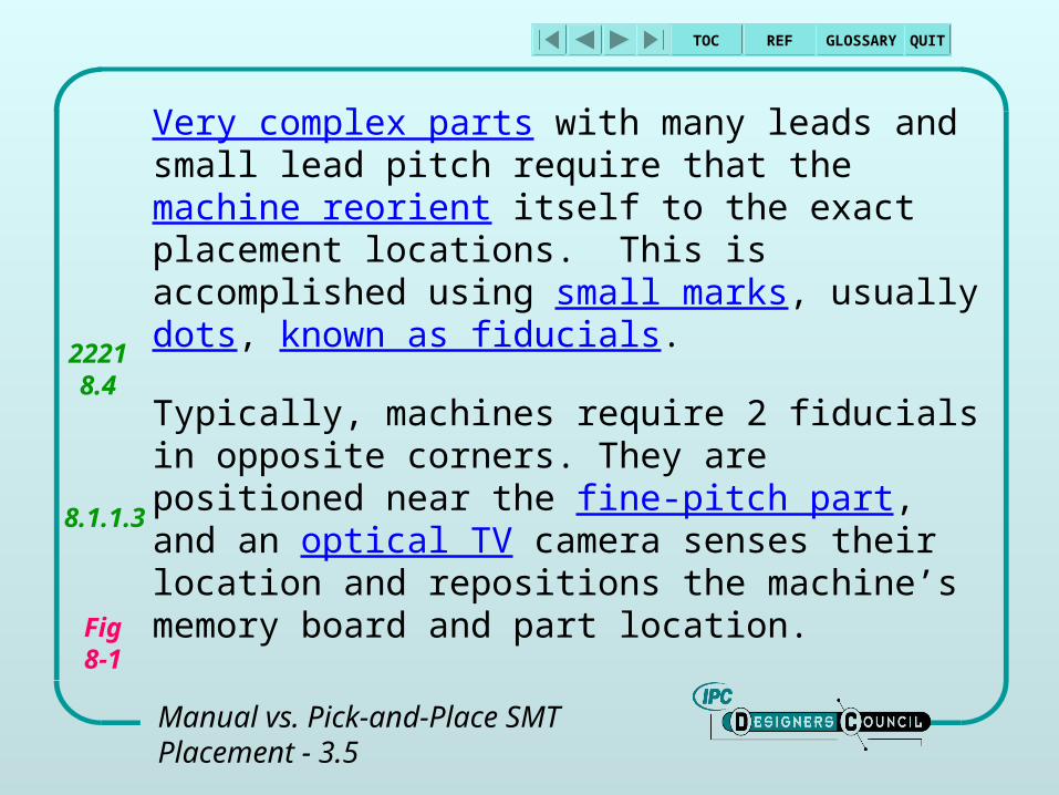
Very complex parts with many leads and small lead pitch require that the machine reorient itself to the exact placement locations. This is accomplished using small marks, usually dots, known as fiducials.
Typically, machines require 2 fiducials in opposite corners. They are positioned near the fine-pitch part, and an optical TV camera senses their location and repositions the machine’s memory board and part location.
22218.4
8.1.1.3
Fig8-1

TOC REF GLOSSARY QUIT
Section 3.6
DIP and SIP Components
Component and Assembly Issues
TOC REF GLOSSARY QUIT
DIP and SIP Components - 3.6
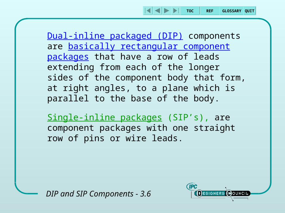
Dual-inline packaged (DIP) components are basically rectangular component packages that have a row of leads extending from each of the longer sides of the component body that form, at right angles, to a plane which is parallel to the base of the body.
Single-inline packages (SIP’s), are component packages with one straight row of pins or wire leads.
TOC REF GLOSSARY QUIT
DIP and SIP Components - 3.6
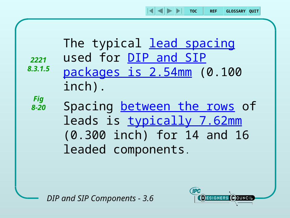
The typical lead spacing used for DIP and SIP packages is 2.54mm (0.100 inch).
Spacing between the rows of leads is typically 7.62mm (0.300 inch) for 14 and 16 leaded components.
22218.3.1.5
Fig8-20
TOC REF GLOSSARY QUIT
DIP and SIP Components - 3.6
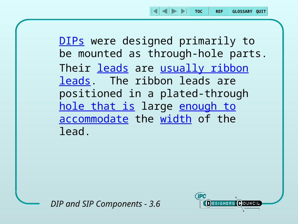
DIPs were designed primarily to be mounted as through-hole parts. Their leads are usually ribbon leads. The ribbon leads are positioned in a plated-through hole that is large enough to accommodate the width of the lead.
TOC REF GLOSSARY QUIT
DIP and SIP Components - 3.6
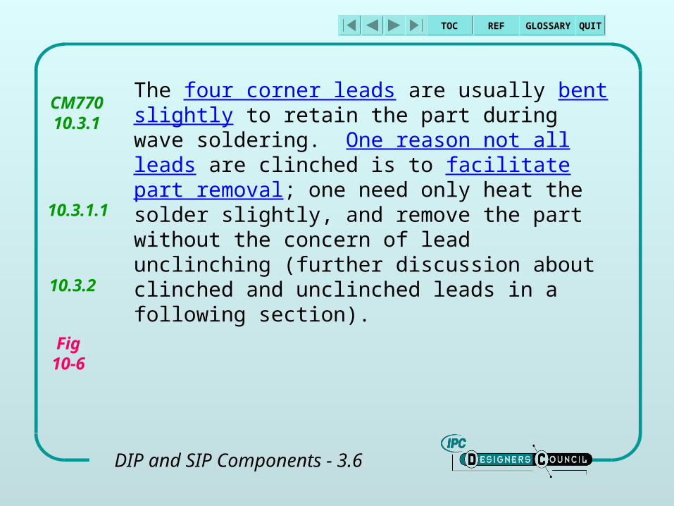
The four corner leads are usually bent slightly to retain the part during wave soldering. One reason not all leads are clinched is to facilitate part removal; one need only heat the solder slightly, and remove the part without the concern of lead unclinching (further discussion about clinched and unclinched leads in a following section).
CM77010.3.1
10.3.1.1
10.3.2
Fig10-6
TOC REF GLOSSARY QUIT
DIP and SIP Components - 3.6
Both DIPs and SIP’s have surface mount capability. The requirements being that the leads must be formed on a mandrel with specific tooling to ensure proper bending of the lead into a surface mount gull wing configuration.
One caution is that the plastic of the DIP and SIP are not necessarily designed to withstand the heat of reflow soldering, therefore, special attention is required to make certain that the body of the part is compatible with the assembly process.
CM77010.3.1.2
10.3.2
Fig10-7
TOC REF GLOSSARY QUIT
Section 3.7
DIP and Chip Carrier Sockets
Component and Assembly Issues
TOC REF GLOSSARY QUIT
DIP and Chip Carrier Sockets - 3.7
Some designs require the use of a socket to interconnect the part to the board. Sockets are usually used if the part to be connected frequently needs replacing or the part cannot tolerate exposure to high soldering temperatures. Most discrete components are not in this category since they were designed to withstand assembly processes.
TOC REF GLOSSARY QUIT
DIP and Chip Carrier Sockets - 3.7
However, occasionally a part must be selected at the time of assembly testing to fine tune the circuit. When this is required, and it is not desired to solder the “as required part” in place, sockets may be used for the discrete part. In this instance they are a low-profile part, of a grip-type device, that are like miniature connectors with a single metal contact for each of the leads of the component.
22218.2.5.2
Extra1.13
TOC REF GLOSSARY QUIT
DIP and Chip Carrier Sockets - 3.7
The use of sockets for semiconductor devices is much more prevalent especially in the frequent up-grading of certain equipment.
The ability to easily remove a part and replace it with one that provides additional capability has been a practice for many years.
TOC REF GLOSSARY QUIT
DIP and Chip Carrier Sockets - 3.7
When sockets are used, their pin numbers are assigned according to the device inserted in the socket. The DIP socket is soldered into the board at the same time the other components are wave soldered. The sockets are low-cost, and can be assembled at high-density, since they are mainly an electro-mechanical part. DIP sockets are generally designed to resist solder wicking into the socket or cavity.
TOC REF GLOSSARY QUIT
DIP and Chip Carrier Sockets - 3.7
When surface mounting first became popular the leadless ceramic chip carrier led the way to show the benefit of very high density circuit designs. Unfortunately, the coefficient of thermal expansion (CTE) of the part did not match that of the printed board. Many articles appeared in technical journals indicating a common problem with cracked solder joints when the CTE mismatch between part and board exceeded the limits of the component to survive the thermal cycles to which it was subjected.
TOC REF GLOSSARY QUIT
DIP and Chip Carrier Sockets - 3.7
As the industry learned about surface mounting many companies switched to leaded parts; others analyzed the amount of solder required and made sure that the solder volume was sufficient to account for the CTE mismatch. Solder gave some of the same compliancy characteristics that were provided by the leads.
TOC REF GLOSSARY QUIT
DIP and Chip Carrier Sockets - 3.7
A third approach was to stay with the leadless chip carrier and provide a socket that could function to accomplish several things. One was to permit ease of installation or replacement of the chip carrier, the other was to eliminate the surface mount CTE mismatch problem.
Extra1.14
TOC REF GLOSSARY QUIT
DIP and Chip Carrier Sockets - 3.7
The chip carrier sockets were designed to be through-hole mounted or surface mounted depending on the termination configuration of the socket contacts. When through-hole mounted, the lead spacing for the chip carrier socket was normally that of the standard 2.54mm [.100"] centers configuration.
TOC REF GLOSSARY QUIT
DIP and Chip Carrier Sockets - 3.7
The surface mount version of the chip carrier socket usually had the additional feature of a mechanical interface. This prevented the stress from different expansion characteristics from getting to the solder joints.
TOC REF GLOSSARY QUIT
DIP and Chip Carrier Sockets - 3.7
In fact some sockets had only a mechanical hold-down and relied on the mechanical contact pressure to interface to the board. The advantage was that the sockets were easy to replace and the board was not damaged due to soldering and desoldering. The disadvantage, however, is that there was now a second mechanical interface in the circuit path.
TOC REF GLOSSARY QUIT
DIP and Chip Carrier Sockets - 3.7
Due to the added cost of the socket and the assembly operation most companies have re-thought the solutions and options available for ease of part exchange or curing CTE mismatch problems.
TOC REF GLOSSARY QUIT
Section 3.8
Clinched and Unclinched Leads
Component and Assembly Issues
TOC REF GLOSSARY QUIT
Clinched and Unclinched Leads - 3.8
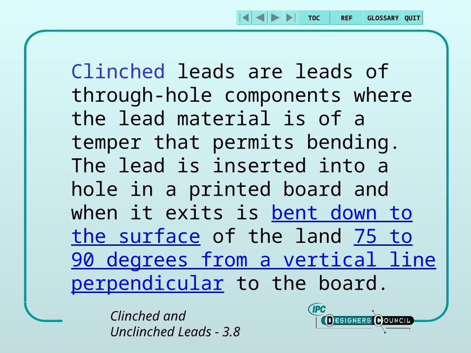
Clinched leads are leads of through-hole components where the lead material is of a temper that permits bending. The lead is inserted into a hole in a printed board and when it exits is bent down to the surface of the land 75 to 90 degrees from a vertical line perpendicular to the board.
TOC REF GLOSSARY QUIT
Clinched and Unclinched Leads - 3.8
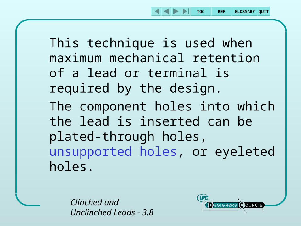
This technique is used when maximum mechanical retention of a lead or terminal is required by the design.
The component holes into which the lead is inserted can be plated-through holes, unsupported holes, or eyeleted holes.
TOC REF GLOSSARY QUIT
Clinched and Unclinched Leads - 3.8
In some designs leads are clinched to adjacent lands where the lead comes through an unsupported hole.
The purpose for this design parameter is that leads can be individually unsoldered and bent straight to allow for easy removal of multiple leaded parts.
22218.3.1.28.3.1.38.3.1.4
TOC REF GLOSSARY QUIT
Clinched and Unclinched Leads - 3.8
Unclinched leads are those that go straight through the board or are partially bent for retention during soldering. If no clinching requirements are specified on the assembly drawing, then unclinched lead termination requirements apply in most instances.
Leads of parts that have hard tempered leads or that of connectors are usually straight through leads. They extend out from the board range of 0.25-2.0mm [.010-.080 inches].
Fig8-19
TOC REF GLOSSARY QUIT
Clinched and Unclinched Leads - 3.8
Clinched leads are not applicable for DIPs. Bends are limited to 30 degrees maximum outward from the axis of the hole with a maximum of 4 leads per component and not more than 2 leads on one side.
22218.3.1.38.3.1.5
Fig8-20
TOC REF GLOSSARY QUIT
Clinched and Unclinched Leads - 3.8
For component mounting requirements in nonplated-through holes (unsupported holes), the leads must be clinched. This is in order to ensure proper solder attachment to the lands of a single sided board. For tempered leads that cannot be clinched, or for leads greater than 1.3mm (.05 inches) in diameter, the hole to lead ratio must be kept as tight as possible in order to ensure a proper solder joint.
TOC REF GLOSSARY QUIT
Section 3.9
Edge Board Connectors
Component and Assembly Issues
TOC REF GLOSSARY QUIT
Edge Board Connectors - 3.9
Edge-board connectors are used to allow the printed board to be “plugged into” the equipment for which it is intended. An edge-board connector is used specifically for making nonpermanent interconnections with the edge-board contacts on a printed board.
Fig8-11
TOC REF GLOSSARY QUIT
Edge Board Connectors - 3.9
These board contacts are near any edge of a board that is designed to mate with the connector. Thus, the configuration uses the board as the plug of the connector system with the plated conductors being the male contacts.
22218.2.5.3
8.2.5.6
Fig8-11
Fig8-12
Fig8-13
Fig8-15
TOC REF GLOSSARY QUIT
Edge Board Connectors - 3.9
Plating on the copper of the board contact varies depending on the amount of insertions to which the connector system must be subjected.
The most popular technique is to plate the copper contact with a nickel plate followed by an over-plate of gold.
TOC REF GLOSSARY QUIT
Edge Board Connectors - 3.9
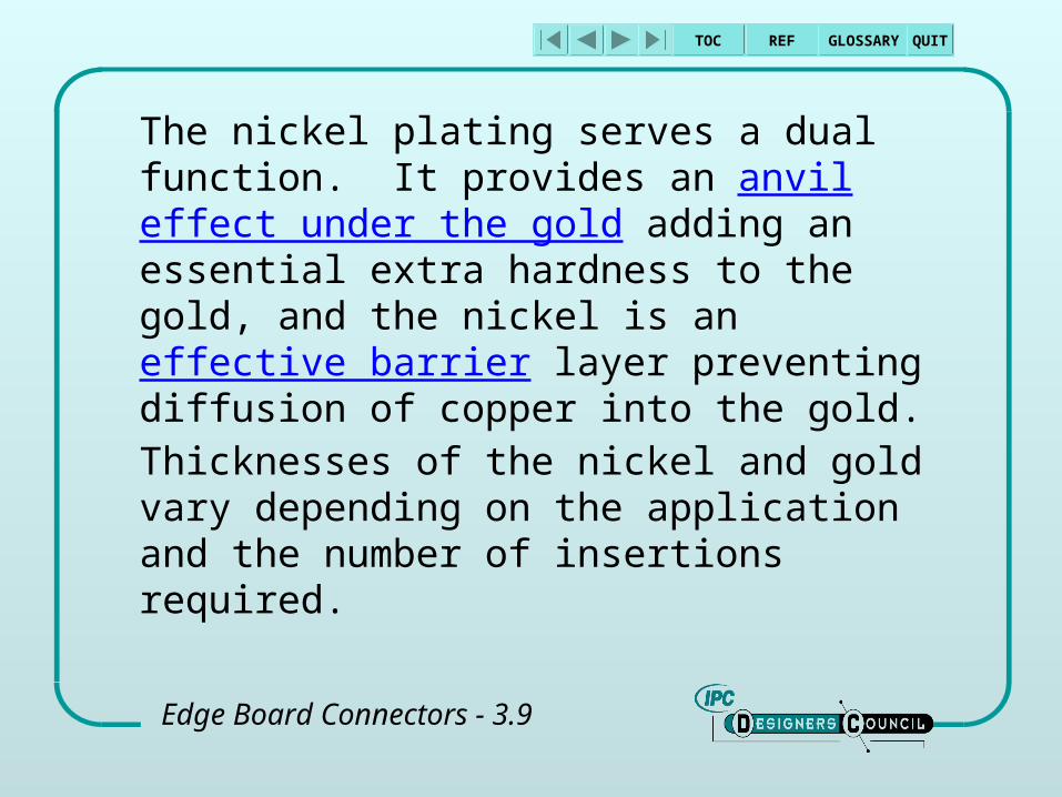
The nickel plating serves a dual function. It provides an anvil effect under the gold adding an essential extra hardness to the gold, and the nickel is an effective barrier layer preventing diffusion of copper into the gold. Thicknesses of the nickel and gold vary depending on the application and the number of insertions required.
TOC REF GLOSSARY QUIT
Edge Board Connectors - 3.9
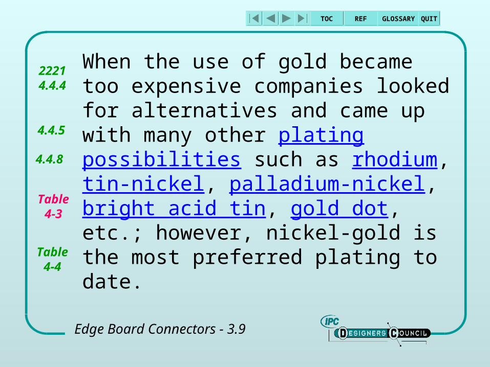
When the use of gold became too expensive companies looked for alternatives and came up with many other plating possibilities such as rhodium, tin-nickel, palladium-nickel, bright acid tin, gold dot, etc.; however, nickel-gold is the most preferred plating to date.
22214.4.4
4.4.5
4.4.8
Table4-3
Table4-4
TOC REF GLOSSARY QUIT
Edge Board Connectors - 3.9
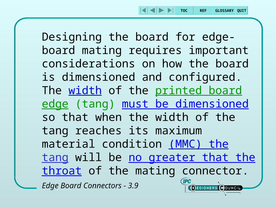
Designing the board for edge-board mating requires important considerations on how the board is dimensioned and configured. The width of the printed board edge (tang) must be dimensioned so that when the width of the tang reaches its maximum material condition (MMC) the tang will be no greater that the throat of the mating connector.
TOC REF GLOSSARY QUIT
Edge Board Connectors - 3.9
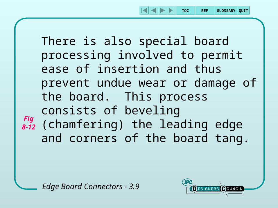
There is also special board processing involved to permit ease of insertion and thus prevent undue wear or damage of the board. This process consists of beveling (chamfering) the leading edge and corners of the board tang.
Fig8-12
TOC REF GLOSSARY QUIT
Edge Board Connectors - 3.9
In addition, some designs require a keying slot to prevent mating the board in the wrong connector. The keying slot must be dimensioned so as not to interfere with the throat of the connector at the time the board keying slot mates with the connector keying pin.
22218.2.5.18.2.5.3
Fig8-11
Fig8-12
Fig8-13
TOC REF GLOSSARY QUIT
Edge Board Connectors - 3.9
With an edge-board connector system the responsibility for proper mating and unmating is shared between the board manufacturer and the connector supplier. At times this can be risky if the system is to be exposed to any severe environmental exposures.
TOC REF GLOSSARY QUIT
Edge Board Connectors - 3.9
One solution is to use a two piece connector system where both portions of the connector interface are made by the connector manufacturer. In this manner the connector system may be proven through stress testing to ascertain that the system will meet the end-use conditions.
22218.2.5.4
8.2.5.5
TOC REF GLOSSARY QUIT
Edge Board Connectors - 3.9
Mounting of the female portion of the two part system is similar to that of mounting a card-edge connector. These are usually mounted on a backplane or mother board with the pins of the connector being soldered or press-fit into plated-through holes of the board.
TOC REF GLOSSARY QUIT
Edge Board Connectors - 3.9
The connector on the plug end is usually positioned where a right angle pin comes out of the connector body at 90 degrees to the board surface.
The right angle pins are soldered into plated-though holes on the daughter board.
22218.2.5.4
8.2.5.5
Fig8-14
TOC REF GLOSSARY QUIT
Edge Board Connectors - 3.9
Mounting of the mother board or backplane and its relationship to the card guides, used to bring the daughter boards into correct alignment with the connector cavities on the motherboard, is critical. A detailed tolerance analysis is required to make certain that the parts align properly. This is done to ensure that the insertion force required to mate the connecting parts is not so great as to damage any of the parts if someone attempts to force the connection.
TOC REF GLOSSARY QUIT
Section 3.10
Bus Bar Mounting Characteristics
Component and Assembly Issues
TOC REF GLOSSARY QUIT
Bus Bar Mounting Characteristics - 3.10
A bus is considered to be one or more conductors used for transmitting data signals or power. In printed board design a bus can also be configured as a plane, such as might be included in a multilayer construction. Therefore, a voltage plane is a conductor layer, or portion of a layer, that serves as a common voltage source at other than ground potential for an electrical circuit, shielding, or heat sinking.
TOC REF GLOSSARY QUIT
Bus Bar Mounting Characteristics - 3.10
This definition is almost identical for a ground plane with the only difference being that the plane serves as a common reference for circuit returns.
Thus a bus bar is thought of as a conduit. The conduit can be a component or a single conductor on a printed board that is used for distributing electrical energy.
TOC REF GLOSSARY QUIT
Bus Bar Mounting Characteristics - 3.10
Bus bars are usually preformed components. They are part of the assembly, just as any other component, and serve the function to provide most, if not all, of the power and ground distribution.
22218.2.13
CM770Fig17-10
CM770Fig17-11
TOC REF GLOSSARY QUIT
Bus Bar Mounting Characteristics - 3.10
The primary reason for using a separate bus bar as opposed to having a plane or printed conductor on the printed board, is that it conserves the real estate of the board for more signal routing.
TOC REF GLOSSARY QUIT
Bus Bar Mounting Characteristics - 3.10
Many electrical engineering views are that to have a substantial voltage and ground, copper or other metals are necessary (i.e. bus bar). By using the separately manufactured bus bar component it minimizes the use of board circuitry for power and/or ground distribution.
22218.2.13
CM770Fig17-10
Fig17-11
TOC REF GLOSSARY QUIT
The number of conductor levels in the bus bar depends on the application. In fact, the application controls many of the physical characteristics of the bus bar itself, or the bus bar system.
Bus Bar Mounting Characteristics - 3.10
TOC REF GLOSSARY QUIT
In normal printed board component mounting requirements one of the rules is to never have more than one lead in a plated-through hole. Bus bars are the only physical components permitted to violate those rules. Some bus bar systems have the leads of the bus bar share the same holes as the integrated circuit and in several instances have been placed under ICs in DIP configurations.
22218.2.13
CM770Fig17-10
Fig17-11
Bus Bar Mounting Characteristics - 3.10
TOC REF GLOSSARY QUIT
Bus Bar Mounting Characteristics - 3.10
The number of terminals, the size and finish of the terminals, and the dielectric strength of the insulation around the bus bar or between bus bar conductor levels is determined as part of the electronic packaging strategy.
The interface between the bus bar and the printed board is usually at the plated-through hole. In addition, this interface should be in a uniform termination pattern.
TOC REF GLOSSARY QUIT
Bus Bar Mounting Characteristics - 3.10
All of these parameters should be defined in the procurement document that defines the characteristics of the bus bar, and the assembly drawing that specifies the sequence of assembly and the use of automated or manual techniques required to complete the assembly operation.
22218.2.13
CM770Fig17-10
Fig17-11
TOC REF GLOSSARY QUIT
Section 3.11
Purpose of Eyelets
Component and Assembly Issues
TOC REF GLOSSARY QUIT
Purpose of Eyelets - 3.11
An eyelet is a short metallic tube the ends of which can be formed outward in order to fasten it within a hole in material such as a printed board. Eyelets have been used for many years. Their primary purpose is to provide mechanical support to the printed board.
Extra1.15
TOC REF GLOSSARY QUIT
Purpose of Eyelets - 3.11
They are accepted in most designs when they perform a mechanical function. Examples of their use are as reinforcement for card puller holes where a metal hook is inserted in the eyeleted hole so that the board assembly can be dislodged from the connector, and reinforcement for mechanical hardware hold down (screws, studs, etc.).
TOC REF GLOSSARY QUIT
Purpose of Eyelets - 3.11
In the early days of printed circuit technology eyelets were also used to provide electrical interconnection from one side of a printed board to another. Under these design rules eyelets were treated exactly like terminals and were soldered to the land patterns. But, if both sides were not soldered simultaneously the possibility existed for developing cold solder joints.
TOC REF GLOSSARY QUIT
Purpose of Eyelets - 3.11
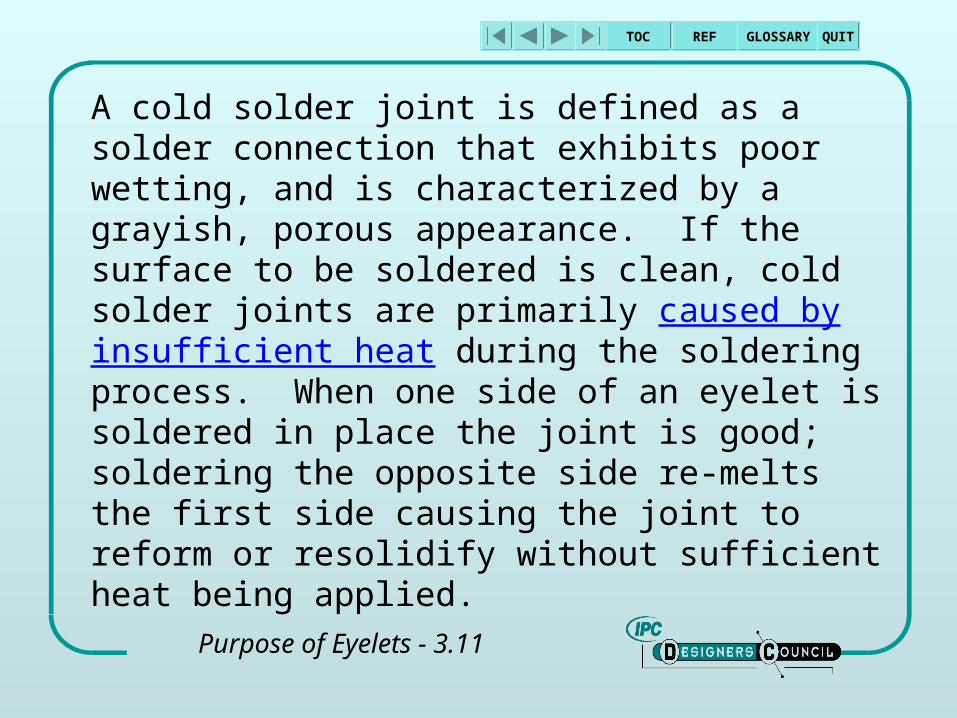
A cold solder joint is defined as a solder connection that exhibits poor wetting, and is characterized by a grayish, porous appearance. If the surface to be soldered is clean, cold solder joints are primarily caused by insufficient heat during the soldering process. When one side of an eyelet is soldered in place the joint is good; soldering the opposite side re-melts the first side causing the joint to reform or resolidify without sufficient heat being applied.
TOC REF GLOSSARY QUIT
Purpose of Eyelets - 3.11
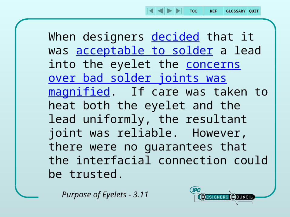
When designers decided that it was acceptable to solder a lead into the eyelet the concerns over bad solder joints was magnified. If care was taken to heat both the eyelet and the lead uniformly, the resultant joint was reliable. However, there were no guarantees that the interfacial connection could be trusted.
TOC REF GLOSSARY QUIT
Purpose of Eyelets - 3.11
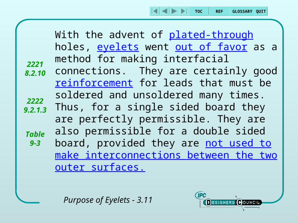
With the advent of plated-through holes, eyelets went out of favor as a method for making interfacial connections. They are certainly good reinforcement for leads that must be soldered and unsoldered many times. Thus, for a single sided board they are perfectly permissible. They are also permissible for a double sided board, provided they are not used to make interconnections between the two outer surfaces.
22218.2.10
22229.2.1.3
Table9-3
TOC REF GLOSSARY QUIT
Purpose of Eyelets - 3.11
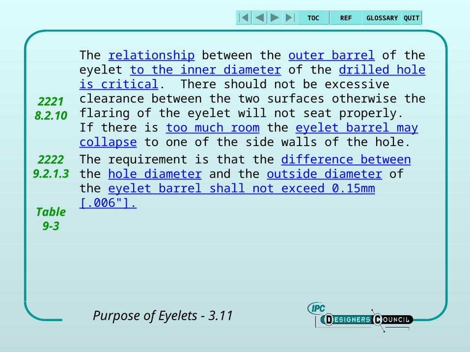
The relationship between the outer barrel of the eyelet to the inner diameter of the drilled hole is critical. There should not be excessive clearance between the two surfaces otherwise the flaring of the eyelet will not seat properly. If there is too much room the eyelet barrel may collapse to one of the side walls of the hole.
The requirement is that the difference between the hole diameter and the outside diameter of the eyelet barrel shall not exceed 0.15mm [.006"].
22218.2.10
22229.2.1.3
Table9-3
TOC REF GLOSSARY QUIT
Section 3.12
Point-to-Point (Jumper) Wires
Component and Assembly Issues
TOC REF GLOSSARY QUIT
Point-to-Point (Jumper) Wires - 3.12
Wires are put on a board to facilitate interconnections between various lands.A point-to-point, or jumper wire is a discrete electrical connection that is part of the basic conductive pattern formed on a printed board. This is opposed to a haywire which is a discrete electrical connection that is added to a printed board to modify the basic conductive pattern formed on the board.
TOC REF GLOSSARY QUIT
Point-to-Point (Jumper) Wires - 3.12
Thus, jumper wires that are a part of the assembly must be clearly defined on the assembly drawing. The wire is not considered part of the printed board but is a part of the assembly process. Adequate provisions for electrical testing should be made where jumper wires are included in the circuit. This is because jumper wires are attached components meaning no electrical connection is present when bare board testing is done (reflected as a discontinuity in the circuit).
Extra1.16
TOC REF GLOSSARY QUIT
Point-to-Point (Jumper) Wires - 3.12
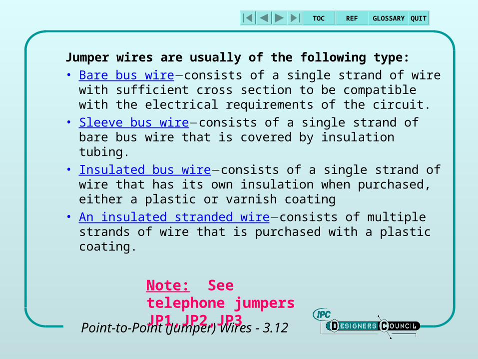
Jumper wires are usually of the following type:• Bare bus wireconsists of a single strand of wire with
sufficient cross section to be compatible with the electrical requirements of the circuit.
• Sleeve bus wireconsists of a single strand of bare bus wire that is covered by insulation tubing.
• Insulated bus wireconsists of a single strand of wire that has its own insulation when purchased, either a plastic or varnish coating
• An insulated stranded wireconsists of multiple strands of wire that is purchased with a plastic coating.
Note: See telephone jumpers JP1,JP2,JP3
TOC REF GLOSSARY QUIT
Point-to-Point (Jumper) Wires - 3.12
They are considered components and should therefore be permanently fixed to the printed board at intervals not to exceed 25.4mm [1.0”].
When bare bus wires are used, they should be no longer than 25.4mm [1.0”] and should never cross over conductors of the bare board.
The shortest XY path for jumper wires should be used unless the board design considerations dictate otherwise.
22218.2.11.1
TOC REF GLOSSARY QUIT
Point-to-Point (Jumper) Wires - 3.12
If the jumper is to be inserted into a through-hole the lead bending requirements should conform to normal component bend radii. The bending feature is predicated by the value of the lead diameter. Jumpers with lead diameters up to 0.75mm [.030"] should have a minimum bend radius of the jumper wire diameter.
TOC REF GLOSSARY QUIT
Point-to-Point (Jumper) Wires - 3.12
Thus, the radius is equal to one diameter. If the jumper wire diameter is larger, the minimum bend radius should be increased.
As an example, for diameters 0.75 to 1.2mm [.030" to .047"] the bend radius is 1.5 diameters, and for larger wires the minimum bend radius is 2 diameters.
22218.1.118.2.11.3
Fig8-9
TOC REF GLOSSARY QUIT
Point-to-Point (Jumper) Wires - 3.12
Sometimes jumpers are attached to terminals. There is a large variety of terminal types. These include single-/double-ended, or single-/multi-sectioned turret solder terminals, as well as bifurcated terminals. When using a turret terminal the jumper is attached by wrapping the lead around the terminal prior to soldering. The leads are wrapped around the terminal a minimum of 180 degrees. If there is more than one lead the leads must not overlap.
Extra3.12
TOC REF GLOSSARY QUIT
Point-to-Point (Jumper) Wires - 3.12
When using bifurcated terminals the jumper wire may be laid straight between the tines of two terminals (though some experts prefer a positive positioning and require that the wire be bent to the side when attached). The details of jumper wire dressing should be documented on the assembly drawing.
The requirements are specified in sufficient detail in the soldering document identified as J-STD-001. This standard was jointly developed by the IPC and the EIA committees.
22218.2.9
8.2.9.1
Fig8-18
8.2.9.2
Fig8-17
TOC REF GLOSSARY QUIT
Point-to-Point (Jumper) Wires - 3.12
Jumpers may also be surface mounted. Some designers have used small zero ohm resistors as jumpers. This technique is quite effective since the parts are added at the same time that other resistors and capacitors are attached. The rules for land patterns and solder joint formation are identical for resistors performing an electrical function as that of the zero ohm resistor.
TOC REF GLOSSARY QUIT
Point-to-Point (Jumper) Wires - 3.12
Also, a wire may be soldered to a surface land as a jumper. When this technique is used it is usually a good idea to stake the wire in position with a dot of adhesive. Glue dots can be added to the assembly automatically. If the wire is in the right orientation it can be soldered to the surface land pattern during the wave solder or reflow solder process.
TOC REF GLOSSARY QUIT
Point-to-Point (Jumper) Wires - 3.12
Round wires can be coined or flattened if they are to be surface mounted. Although this feature is not mandatory, it is good practice so that the surface to surface area between the wire and the land is maximized.
TOC REF GLOSSARY QUIT
Quiz 3
• Which side of the board should through-hole components be mounted on, if the board is to be machine (wave) soldered?– either side of the printed board– both sides of the printed board– the side that is in contact with the solder– the side opposite that which is in contact with the
solder
Answer: the side opposite that which is in contact with the solder
TOC REF GLOSSARY QUIT
Quiz 3
• What is the basic difference in part mounting techniques of SMT vs. through-hole components?– through-holes require plating– SMT devices require no holes– SMT lands are smaller in area– solder joints are formed differently
Answer: SMT devices require no holes

TOC REF GLOSSARY QUIT
Quiz 3
• What is the maximum lead protrusion from the surface of the plating or the foil for standard leaded components attached to the board with straight through leads?– 1.0mm [0.040”]– 1.5mm [0.060”]– 2.0mm [0.080”]– 2.3mm [0.092”]
Answer: 1.5mm [0.060”]
TOC REF GLOSSARY QUIT
Quiz 3
• What is the purpose of the key or keying slot in a two-piece or card-edge connector?– to restrict the use of connector types– to validate the need for two-piece connectors– to prevent improper insertion into the connector– to differentiate between printed board connector
types
Answer: to prevent improper insertion into the connector

TOC REF GLOSSARY QUIT
Quiz 3
• Which aspects of a component data sheet are the most important to facilitate component layout?– the electrical properties– the maximum power consumption– the physical description of the component– the thermal heat distribution characteristics
Answer: the physical description of the component

TOC REF GLOSSARY QUIT
Quiz 3
• How many component leads can be mounted in any one hole used for attaching the component to the circuit pattern?– one lead– no more than two leads– no more than three leads– no more than four leads
Answer: one lead
TOC REF GLOSSARY QUIT
Quiz 3
• What is the primary purpose for breaking up large conductive areas on external layers?– to prevent copper blistering– to enhance copper adhesion– to prevent solder mask blistering– to enhance component soldering
Answer: to prevent solder mask blistering
TOC REF GLOSSARY QUIT
Quiz 3
• What is the most probable cause of a through-hole multilayer board assembly repeatedly containing defective solder joints on the power and ground connections?– the solder dwell is too short– component leads are too large– the board orientation is incorrect– component through-holes are not thermally
relieved
Answer: component through-holes are not thermally relieved