Embed Size (px)
Citation preview

Topic 7
Applying Digital Technology to PWM Control-Loop Designs
M k HMark Hagen
Overview
What do we mean by "Digital Power"
Modeling a mixed analog/digital power supply
Power stage
ControllerCo o e
Effect of quantization
Measuring the transfer function in a digitallyMeasuring the transfer function in a digitally controlled power supply
Application of nonlinear gainApplication of nonlinear gain
Time-model software
7-2
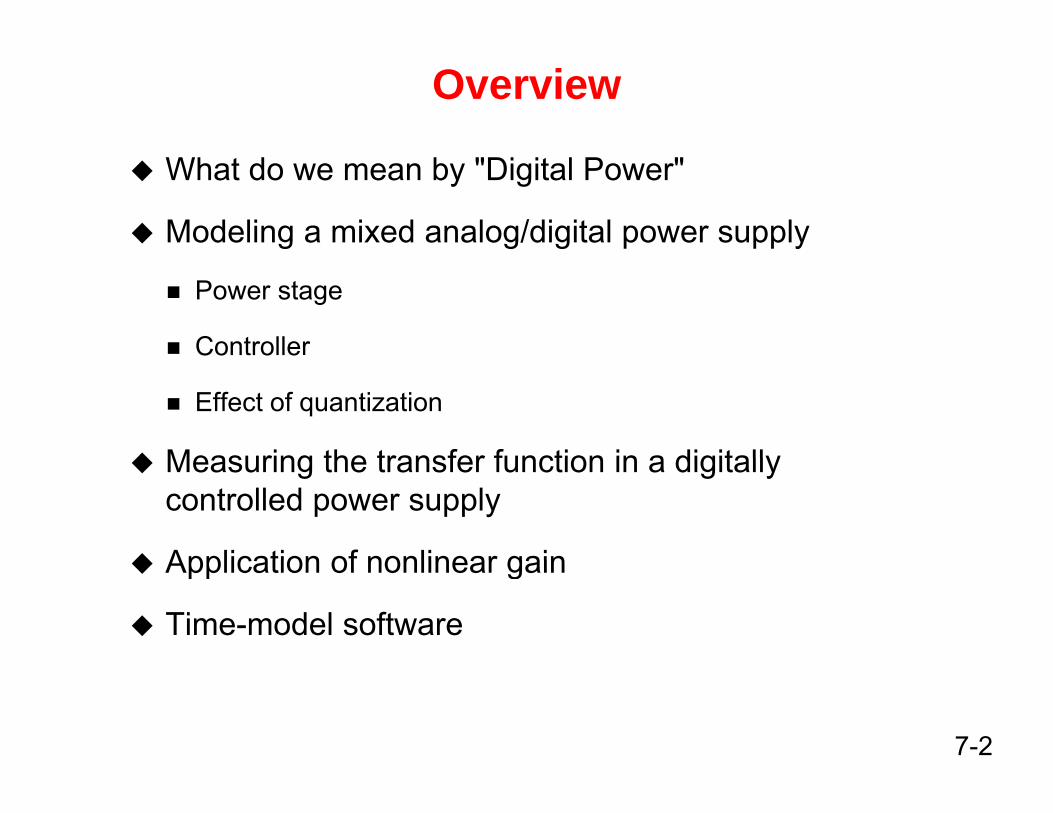
Non-isolated Power
Vg
Vout
RESR
RL2
RL1
L2
L1
i2
i1
R++
Vg
Vout
RESR
RL2
RL1
L2
L1
i2
i1
R+
d[n]
Vsense...c1 c2
e[n] e(t)–
ΣErrorADC
CompensatorG (z)C
DigitalPWM
C+
V–C
–
Compensator
PWM
C+
V–C
–
Set/Measure V ;Report I , I ,
outin out
Vref
Memory
+ADCG (z)CPWM
ProcessingMonitor Memory
DAC
Communication1 2
d(t) e(t)
Vref
++
––
VrampVramp
+
–
"Digital Control" means sampling feedback information and
Digital ControllerAnalog Controller
Temperature andFaults
Memory UnitADC Memory Communication
Digital Control means sampling feedback information and closing the loop numerically
Compensator uses digital signal processing techniques to construct the control effort for the PWM
7-3
the control effort for the PWM
Enables monitoring of states of the converter
Modeling a Mixed Analog/Digital System
Switch-mode power supplies (SMPS) have always had a digital component; they have a control-effort update interval equal to the switching periodupdate interval equal to the switching period
In a digitally-controlled SMPS, the error amplifier is replaced with an ADC and a digital filterp gThis introduces:
Feedback quantizationControl effort quantizationControl effort quantizationDelay needed to sample the feedback and calculate the control effort
The key to implementing a digitally-controlled power supply is understanding these effects
7-4
First, let's model the system.
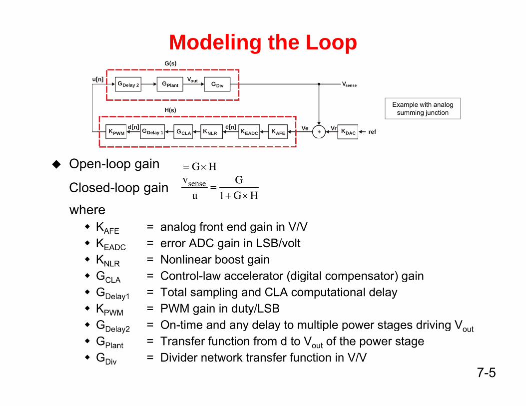
Modeling the LoopG(s)
Example with analog summing junction
GDelay 2 GPlantVout GDiv
d[n] e[n]
u[n]
H(s)
VV
Vsense
Open-loop gain G H= ×G
KPWM KNLR KEADCd[n] e[n]GDelay 1 GCLA KAFE refVrVe KDAC+
Closed-loop gainwhere
KAFE = analog front end gain in V/V
=+ ×
sensev G
u 1 G H
KAFE analog front end gain in V/VKEADC = error ADC gain in LSB/voltKNLR = Nonlinear boost gainGCLA = Control-law accelerator (digital compensator) gainGCLA Co o a acce e a o (d g a co pe sa o ) gaGDelay1 = Total sampling and CLA computational delayKPWM = PWM gain in duty/LSBGDelay2 = On-time and any delay to multiple power stages driving Vout
7-5
Delay2 y y p p g g out
GPlant = Transfer function from d to Vout of the power stageGDiv = Divider network transfer function in V/V
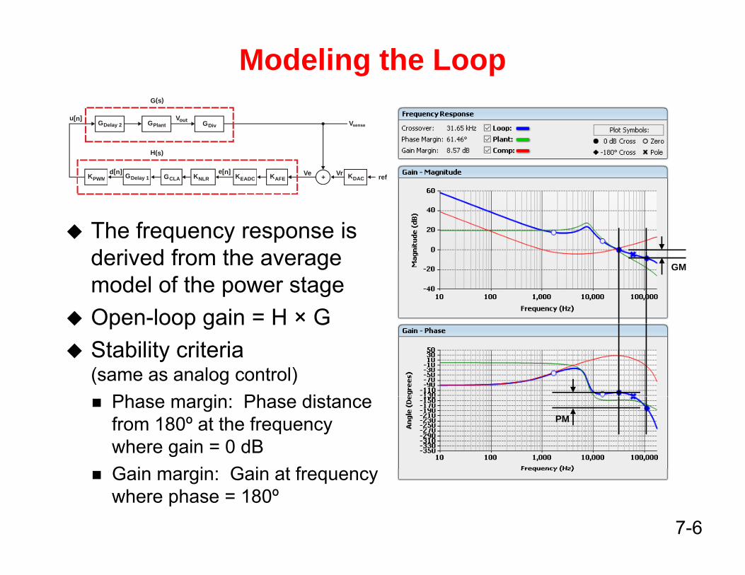
Modeling the LoopG(s)
GDelay 2 GPlantVout GDiv
KPWM KNLR KEADCd[n] e[n]
u[n]
H(s)
GDelay 1 GCLA KAFE refVrVe
Vsense
KDAC+
The frequency response is d i d f th
PWM NLR EADCDelay 1 GCLA AFE refDAC
GMderived from the average model of the power stageOpen-loop gain = H × GOpen loop gain H GStability criteria (same as analog control)
Ph i Ph di tPM
Phase margin: Phase distance from 180º at the frequency where gain = 0 dBG i i G i t f
7-6
Gain margin: Gain at frequency where phase = 180º
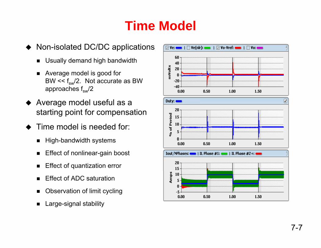
Time ModelNon isolated DC/DC applicationsNon-isolated DC/DC applications
Usually demand high bandwidth
Average model is good for BW << fsw/2. Not accurate as BW approaches fsw/2
Average model useful as astarting point for compensation
Time model is needed for:High bandwidth systemsHigh-bandwidth systems
Effect of nonlinear-gain boost
Effect of quantization error
Effect of ADC saturation
Observation of limit cycling
L i l t bilit
7-7
Large-signal stability
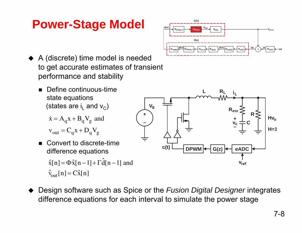
Power-Stage Model GDelay 2 GPlantVout GDiv
u[n]
G(s)
H(s)
Vsense
A (discrete) time model is needed to get accurate estimates of transient
KPWM KNLR KEADCd[n] e[n]GDelay 1 GCLA KAFE refVrVe KDAC+
performance and stability
Define continuous-timestate equations
R L iLL
(states are iL and vC)
q q g
t
x A x B V and
v C x D V
= +
= +
Resr
CR
Hvo
H=1vc+–
Vg
+–
Convert to discrete-time difference equations
out q q gv C x D V= +
ˆˆ ˆ[ ] [ 1] d[ 1] dΦ Γ
c(t) DPWM eADCG(z)
Design software such as Spice or the Fusion Digital Designer integrates
out
ˆ ˆx[n] x[n 1] d[n 1] and
ˆ ˆv [n] Cx[n]
= Φ − +Γ −=
vref
7-8
Design software such as Spice or the Fusion Digital Designer integrates difference equations for each interval to simulate the power stage
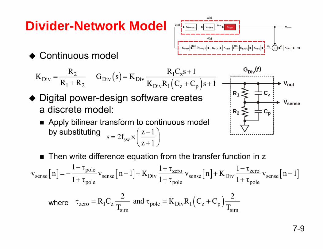
Divider-Network Model GDelay 2 GPlantVout
d[n] e[n]
u[n]
G(s)
H(s)
VrVe
VsenseGDiv
Continuous model
2Di
RK = ( ) 1 z
Di DiR C s 1
G s K+
=
KPWM KNLR KEADCd[n] e[n]GDelay 1 GCLA KAFE refVrVe KDAC+
G (f)Div
Digital power-design software creates a discrete model:
Div1 2
KR R
=+
( ) ( )Div DivDiv 1 z p
G s KK R C C s 1
=+ +
R1 Cz
Vout
Vsensea discrete model:
Apply bilinear transform to continuous model by substituting
swz 1
s 2f1
−⎛ ⎞= ×⎜ ⎟⎝ ⎠
CpR2
Then write difference equation from the transfer function in z
sw z 1⎜ ⎟+⎝ ⎠
[ ] [ ] [ ] [ ]pole zero zero1 1 1
1 K K 1− τ + τ − τ
where ( )zero 1 z pole Div 1 z p2 2
R C and K R C Cτ = τ = +
[ ] [ ] [ ] [ ]p zero zerosense sense Div sense Div sense
pole pole pole
v n v n 1 K v n K v n 11 1 1
= − − + + −+ τ + τ + τ
7-9
where ( )zero 1 z pole Div 1 z psim sim
R C and K R C CT T
τ τ +
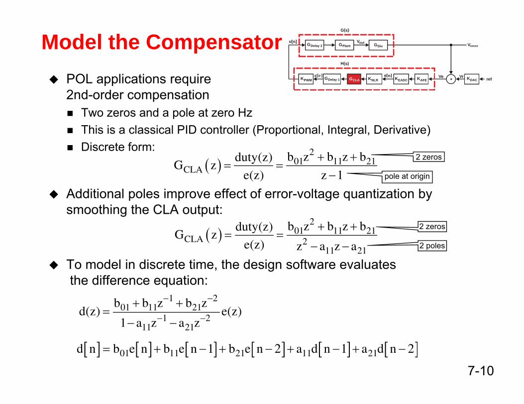
Model the CompensatorPOL li ti i
GDelay 2 GPlantVout
d[ ] e[ ]
u[n]
G(s)
H(s)
VsenseGDiv
POL applications require 2nd-order compensation
Two zeros and a pole at zero HzThi i l i l PID t ll (P ti l I t l D i ti )
KPWM KNLR KEADCd[n] e[n]GDelay 1 KAFE refVrVe KDAC+GCLA
This is a classical PID controller (Proportional, Integral, Derivative)Discrete form:
( )2
01 11 21CLA
b z b z bduty(z)G z
e(z) z 1
+ += =
−2 zeros
pole at origin
Additional poles improve effect of error-voltage quantization by smoothing the CLA output:
e(z) z 1
201 11 21b z b z bduty(z) + +
pole at origin
2 zeros
To model in discrete time, the design software evaluatesthe difference equation:
( ) 01 11 21CLA 2
11 21
b z b z bduty(z)G z
e(z) z a z a
+ += =
− −
2 zeros
2 poles
the difference equation:1 2
01 11 211 2
11 21
b b z b zd(z) e(z)
1 a z a z
− −
− −+ +
=− −
7-10[ ] [ ] [ ] [ ] [ ] [ ]01 11 21 11 21d n b e n b e n 1 b e n 2 a d n 1 a d n 2= + − + − + − + −
11 21
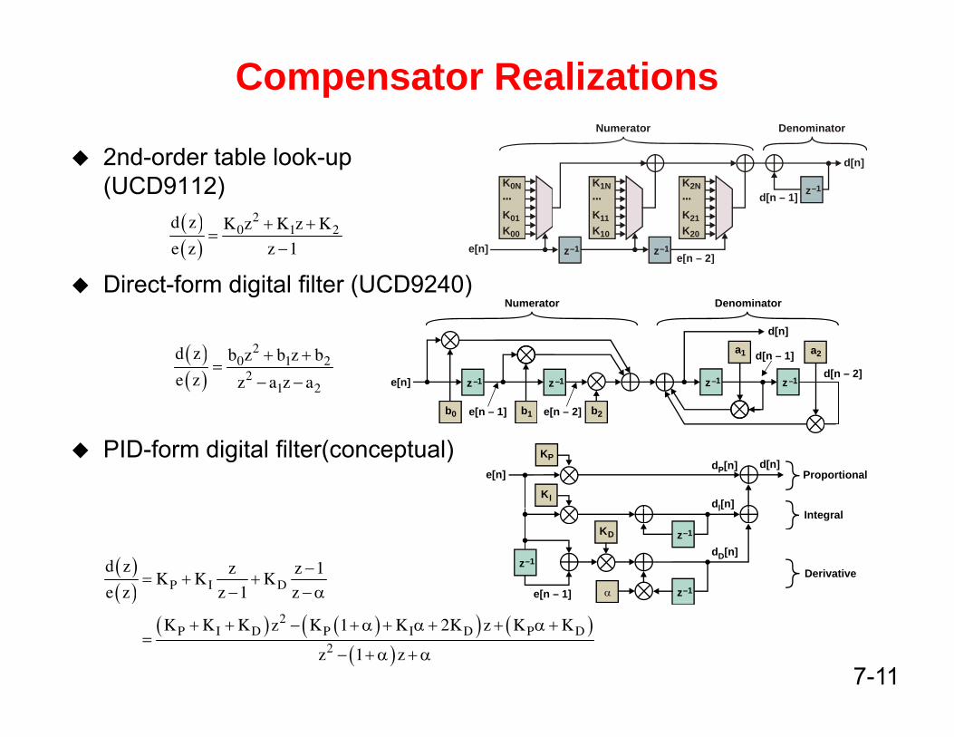
Compensator RealizationsNumerator Denominator
2nd-order table look-up(UCD9112)
( ) 20 1 2d z K z K z K+ +
d[n 1] –
d[n]
K0N K1N K2N
K K K
z–1
K01 K11 K21
... ... ...... ... ...
Direct-form digital filter (UCD9240)
( )( )
0 1 2
e z z 1=
− e[n]e[n 2]–
K00 K10 K20
z–1 z–1
Numerator Denominator
( )( )
20 1 2
21 2
d z b z b z b
e z z a z a
+ +=
− − e[n]
e[n – 1] e[n – 2]
z–1 z–1
b0 b1 b2
d[n – 1]d[n – 2]
d[n]
z–1z–1
a1 a2
PID-form digital filter(conceptual)
e[n 1] e[n 2]0 1 2
e[n]
KP
Kl
d [n]P
d [n]l
d[n]Proportional
( )( ) P I D
d z z z 1K K K
e z z 1 z
−= + +
− −α
z–1
z–1
z–1
e[n – 1]
KD
α
d [n]D
[ ]lIntegral
Derivative
7-11
( )( ) ( )( ) ( )
( )
2P I D P I D P D
2
K K K z K 1 K 2K z K K
z 1 z
+ + − +α + α + + α +=
− +α +α
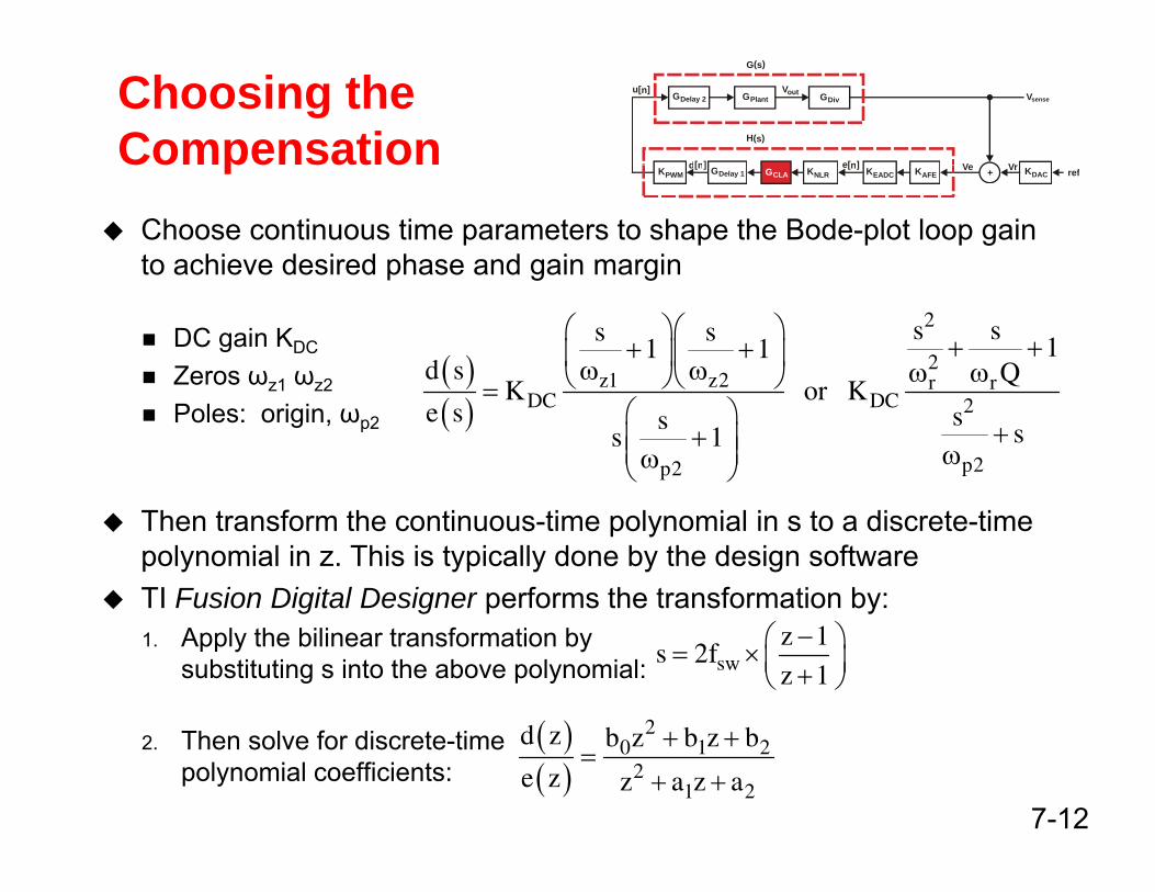
Choosing the Compensation
GDelay 2 GPlantVout
d[n] e[n]
u[n]
G(s)
H(s)
VrVe
VsenseGDiv
Co pe sat oChoose continuous time parameters to shape the Bode-plot loop gain to achieve desired phase and gain margin
KPWM KNLR KEADCd[n] e[n]GDelay 1 KAFE refVrVe KDAC+GCLA
p g g
DC gain KDC
Zeros ωz1 ωz2 ( )2
2z1 z2 r r
s ss s11 1
d s QK or K
⎛ ⎞⎛ ⎞+ ++ +⎜ ⎟⎜ ⎟ω ω ω ω⎝ ⎠⎝ ⎠=z1 z2
Poles: origin, ωp2 ( ) DC DC 2
p2p2
K or Ke s ss ss 1
=⎛ ⎞
++⎜ ⎟⎜ ⎟ ωω⎝ ⎠
Then transform the continuous-time polynomial in s to a discrete-time polynomial in z. This is typically done by the design softwareTI Fusion Digital Designer performs the transformation by:1. Apply the bilinear transformation by
substituting s into the above polynomial:
( ) 2d b b b
swz 1
s 2fz 1
−⎛ ⎞= ×⎜ ⎟+⎝ ⎠
7-12
2. Then solve for discrete-time polynomial coefficients:
( )( )
20 1 2
21 2
d z b z b z b
e z z a z a
+ +=
+ +
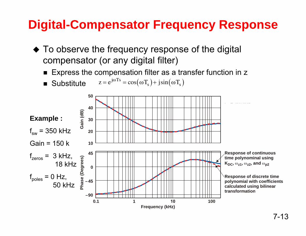
Digital-Compensator Frequency Response
To observe the frequency response of the digital compensator (or any digital filter)
Express the compensation filter as a transfer function in zExpress the compensation filter as a transfer function in zSubstitute ( ) ( )j Ts
s sz e cos T jsin Tω= = ω + ω
ExampleF = 350 kHz
50
Example :
fsw = 350 kHz
F = 350 kHzGain = 150 kF = 3 kHz, 18 kHzF = 0 Hz, 50 kHz
s
zerospoles
40
30
20
Gai
n (d
B)
fsw 350 kHz
Gain = 150 k
fzeros = 3 kHz, 18 kH
Response of continuous time polynominal using K andω ω ω
0
10
45
ees)
18 kHz
fpoles = 0 Hz, 50 kHz
Response of discrete time polynomial with coefficients calculated using bilinear transformation
K , , , and DC z1 z2 p2ω ω ω0
–45
Phas
e (D
egre
7-13
0.1 100
transformation
1Frequency (kHz)
–90
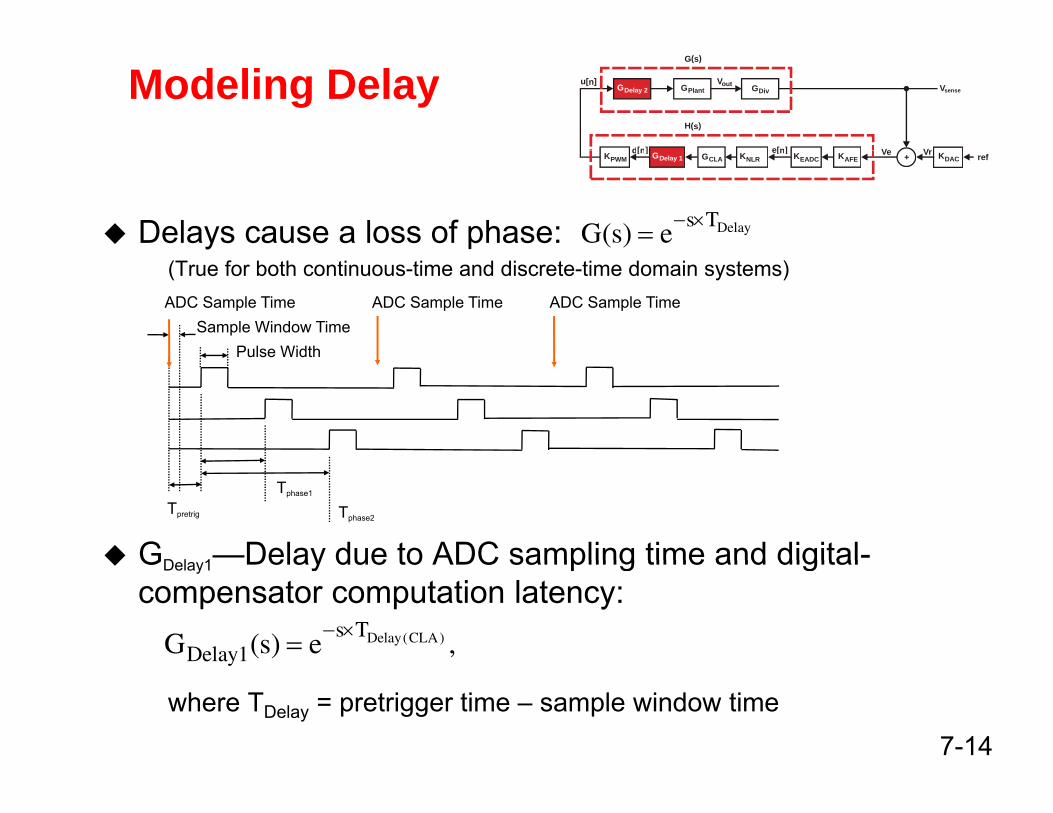
Modeling Delay GPlantVout
d[n] e[n]
u[n]
G(s)
H(s)
VrVe
VsenseGDivGDelay 2
Delays cause a loss of phase:
KPWM KNLR KEADCd[n] e[n]
KAFE refVrVe KDAC+GCLAGDelay 1
Delays TG(s) e
− ×=(True for both continuous-time and discrete-time domain systems)ADC Sample Time
Sample Window TimePulse Width
ADC Sample Time ADC Sample Time
Pulse Width
GD l 1—Delay due to ADC sampling time and digital-Tpretrig
Tphase1
Tphase2
GDelay1 Delay due to ADC sampling time and digitalcompensator computation latency:
Delay(CLA)s TDelay1G (s) e ,
− ×=
7-14where TDelay = pretrigger time – sample window time
y
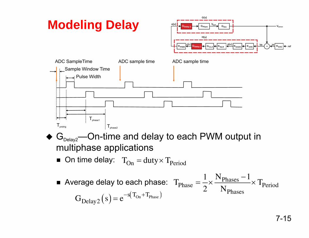
Modeling Delay GPlantVout
d[n] e[n]
u[n]
G(s)
H(s)
VV
VsenseGDivGDelay 2
ADC SampleTimeSample Window Time
ADC sample time ADC sample time
KPWM KNLR KEADCd[n] e[n]
KAFE refVrVe KDAC+GCLAGDelay 1
Pulse Width
G O ti d d l t h PWM t t iTpretrig
Tphase1
Tphase2
GDelay2—On-time and delay to each PWM output in multiphase applications
On time delay: On PeriodT duty T= ×
Average delay to each phase:
On Periody
( ) ( )s T T+
PhasesPhase Period
Phases
N 11T T
2 N
−= × ×
7-15
( ) ( )On Phases T TDelay2G s e− +=
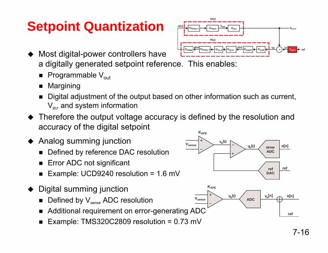
Setpoint Quantization GPlantVout
d[ ] e[ ]
u[n]
G(s)
H(s)
VsenseGDivGDelay 2
Most digital-power controllers have a digitally generated setpoint reference. This enables:
Programmable Vout
KPWM KNLR KEADCd[n] e[n]
KAFE refVrVe +GCLAGDelay 1 KDAC
g out
MarginingDigital adjustment of the output based on other information such as current, Vin, and system information
Therefore the output voltage accuracy is defined by the resolution and accuracy of the digital setpoint
Analog summing junctionKAFE
v (t)o+Analog summing junction
Defined by reference DAC resolutionError ADC not significantExample: UCD9240 resolution = 1 6 mV
errorADC
refDAC
e[n]Vsensev (t)o
v (t)e
ref
–+
–
Digital summing junctionDefined by Vsense ADC resolution
Example: UCD9240 resolution = 1.6 mV
ADC
KAFE
Vsensev (t)o v [n]o e[n]+
–
7-16
Additional requirement on error-generating ADCExample: TMS320C2809 resolution = 0.73 mV
ref
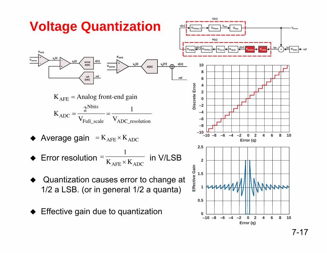
Voltage Quantization GPlantVout
d[n] e[n]
u[n]
G(s)
H(s)
VV
VsenseGDivGDelay 2
KPWM KNLRd[n] e[n]
refVrVe +GCLAGDelay 1 KDACKEADC KAFE
1086
errorADC
refDAC
e[n]
KAFE
Vsensev (t)o
v (t)e
ref
+
–+
–
ADC
KAFE
Vsensev (t)o v [n]o
ref
e[n]+
–
AFE
Nbits
K Analog front-end gain
2 1
=
Dis
cret
e Er
ror
6420
–24
DAC ref
Average gain
ADCFull_scale ADC_resolution
2 1K
V V= =
AFE ADCK K= × –8 –6 –4 –2 0Error (q)
2 4 6 8 10–10
–4–6–8
–10
Error resolution in V/LSBAFE ADC
1
K K=
×
Gai
n
2.5
2
1.5
Quantization causes error to change at1/2 a LSB. (or in general 1/2 a quanta) Ef
fect
ive 1.5
1
0.5
7-17
Effective gain due to quantization –8 –6 –4 –2 0
Error (q)2 4 6 8 10–10
0
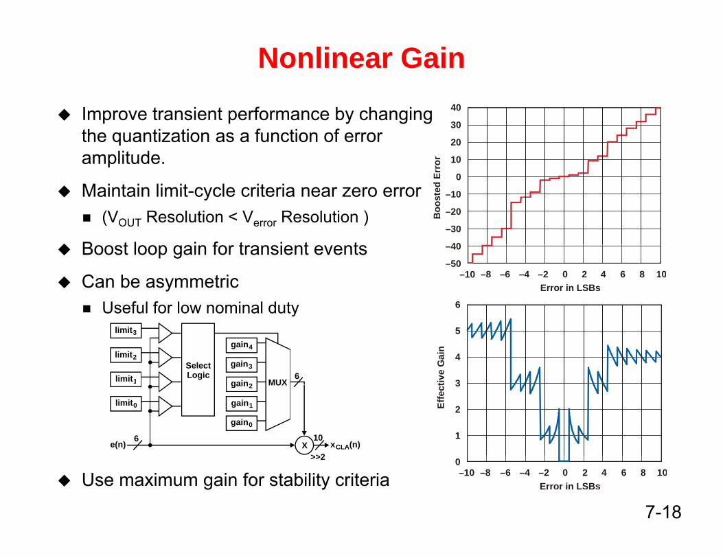
Nonlinear Gain
Improve transient performance by changing the quantization as a function of error amplitude.
Erro
r
40
30
20
10
0
Maintain limit-cycle criteria near zero error(VOUT Resolution < Verror Resolution )
B t l i f t i t t
Boo
sted
E 0
–10
–20
–30
40Boost loop gain for transient events
Can be asymmetricUseful for low nominal duty
–8 –6 –4 –2 0Error in LSBs
2 4 6 8 10–10
–40
–50
6y
6limit1
limit2
limit3
gain2
gain3
gain4
SelectLogic
MUX tive
Gai
n
5
4
3
x (n)CLAe(n)>>2
106X
limit0
gain0
gain1
gain2 MUX
Effe
ct 3
2
1
7-18
Use maximum gain for stability criteria>>2
–8 –6 –4 –2 0Error in LSBs
2 4 6 8 10–100
Nonlinear Boost
Scope traces with and without nonlinear boost
1 3
P k tRMS Error
D i
1.3
1.25
1.2
1 15no boost
rmspk-pk
Parameter
Peak-to-Peak Output
ExcursionUniform gain of 1X 130.5 mV 5.2 mVGain boosted 3X for 108.1 mV 5.0 mV
DuringQuiescentOperation
V (V
)ou
t
1.15
1.1
1.05
1 4X b t
3X boost
Ga boosted 3 o |v | > 5err
Gain boosted 4X for |v | > 5err
88.4 mV 5.0 mV
1
0.95
0.9
0.85load current
4X boost
0 200 600 800 1000Time (µs)
4000.8
7-19
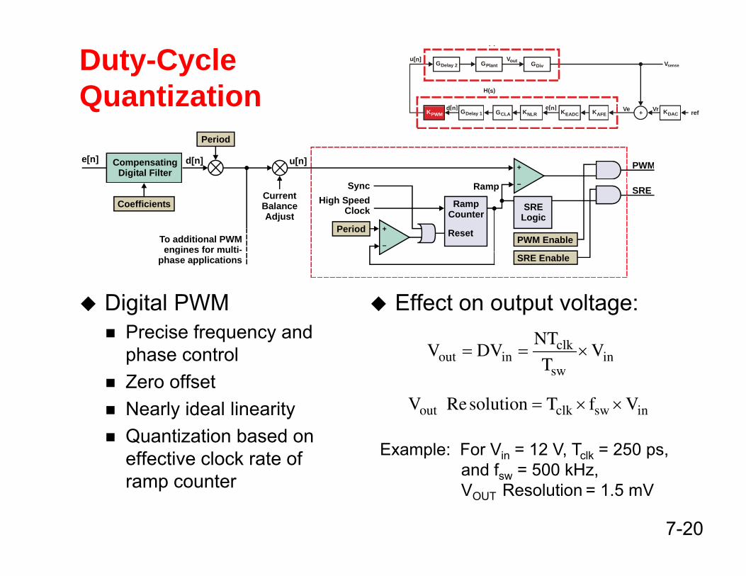
Duty-Cycle Quantization
GPlantVout
d[ ] e[ ]
u[n]
( )
H(s)
VsenseGDivGDelay 2
Qua t at oKNLR
d[n] e[n]refVrVe +GCLAGDelay 1 KDACKEADC KAFEKPWM
e[n] CompensatingDigital Filter
d[n]
Period
PWMu[n]+
CurrentBalanceAdjust
To additional PWMengines for multi-
Period
Coefficients RampC ounter
SRELogic
Reset
SRE
PWM Enable
RampHigh Speed
Clock
Sync
+
–
–
Digital PWM Effect on output voltage:
engines for multiphase applications SRE Enable
Precise frequency and phase controlZero offset
clkout in in
sw
NTV DV V
T= = ×
Nearly ideal linearityQuantization based on effective clock rate of
out clk sw inV Resolution T f V= × ×
Example: For Vin = 12 V, Tclk = 250 ps, and f = 500 kHz
7-20
ramp counter and fsw = 500 kHz,VOUT Resolution = 1.5 mV
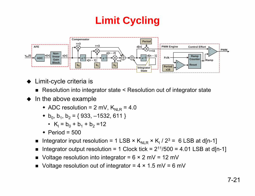
Limit Cycling
ADCNon-linearGain
AFE
e[n]v (t)en
Compensator
x[n]x[n – 1]
z–1
x[n – 2]
z 1–
Period
d[n – 1]
>>11
>>3
>>3>>3
d[n]
z 1– RampC ounter
PWMPWM Engine
Ramp
Control Effort
Fclk
+
–
Limit-cycle criteria is
Blockx[n 1]
b0 b1 b2
>>3
Periodx16
ResetRamp
+
–IntegratorS tate
Resolution into integrator state < Resolution out of integrator stateIn the above example
ADC resolution = 2 mV, KNLR = 4.0NLR
b0, b1, b2 = { 933, –1532, 611 }• KI = b0 + b1 + b2 =12Period = 500
Integrator input resolution = 1 LSB × KNLR × KI / 23 = 6 LSB at d[n-1]Integrator output resolution = 1 Clock tick = 211/500 = 4.01 LSB at d[n-1]Voltage resolution into integrator = 6 × 2 mV = 12 mV
7-21
g gVoltage resolution out of integrator = 4 × 1.5 mV = 6 mV
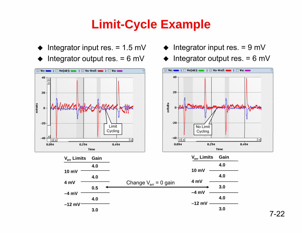
Limit-Cycle Example
Integrator input res. = 1.5 mVIntegrator output res. = 6 mV
Integrator input res. = 9 mVIntegrator output res. = 6 mV
Limit Cycling
No Limit Cycling
Verr Limits Gain Verr Limits Gain
Cycling Cycling
err
4.010 mV
4.04 mV
0.5
4.010 mV
4.04 mV
3.0Change Verr = 0 gain
7-22
–4 mV4.0
–12 mV3.0
–4 mV4.0
–12 mV3.0
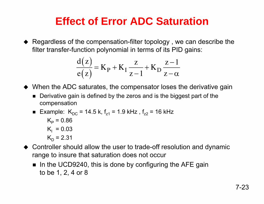
Effect of Error ADC Saturation
Regardless of the compensation-filter topology , we can describe the filter transfer-function polynomial in terms of its PID gains:
( )d z z z 1−
When the ADC saturates, the compensator loses the derivative gain
( )( ) P I D
d z z z 1K K K
e z z 1 z= + +
− −α
, p gDerivative gain is defined by the zeros and is the biggest part of the compensationExample: KDC = 14.5 k, fz1 = 1.9 kHz , fz2 = 16 kHzDC z1 z2
KP = 0.86KI = 0.03KD = 2.31 D
Controller should allow the user to trade-off resolution and dynamic range to insure that saturation does not occur
In the UCD9240, this is done by configuring the AFE gain
7-23
In the UCD9240, this is done by configuring the AFE gain to be 1, 2, 4 or 8
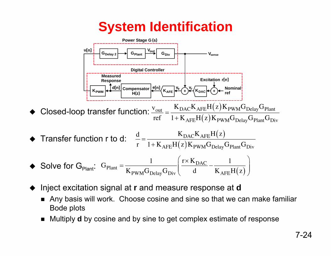
System Identification Power Stage G (s)
r[n]Excitation
VsenseGDelay 2 GPlantVout GDiv
u[n]
Digital ControllerMeasured R
Closed-loop transfer function: ( )DAC AFE PWM Delay PlantoutK K H z K G Gv
=
CompensatorH(z) KPWM
d[n] e[n]
r[n]
ve vrKAFE + +KDAC
Excitation
Nominal ref
Response
Closed-loop transfer function:
Transfer function r to d:
( )AFE PWM Delay Plant Divref 1 K H z K G G G=
+
( )( )
DAC AFEK K H zd
r 1 K H z K G G G=
+
Solve for GPlant: ( )DAC
PlantPWM Delay Div AFE
r K1 1G
K G G d K H z
⎛ ⎞×= −⎜ ⎟⎜ ⎟
⎝ ⎠
( )AFE PWM Delay Plant Divr 1 K H z K G G G+
Inject excitation signal at r and measure response at dAny basis will work. Choose cosine and sine so that we can make familiar Bode plots
7-24
Bode plotsMultiply d by cosine and by sine to get complex estimate of response
System Identification
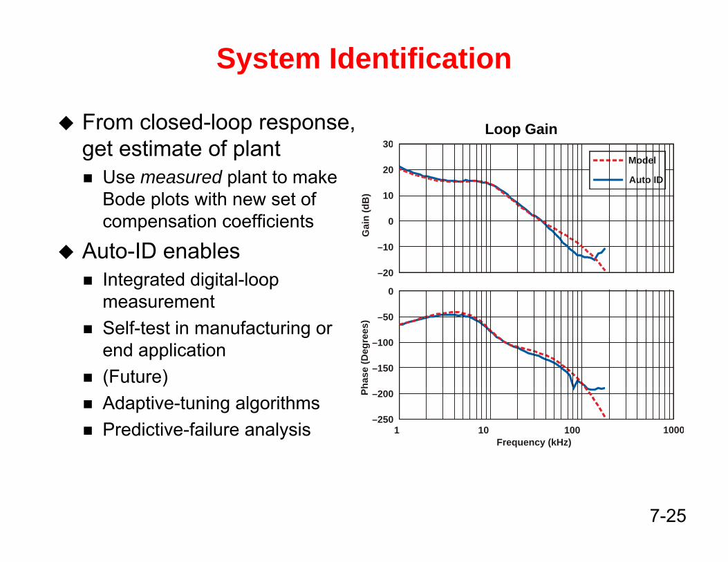
From closed-loop response, get estimate of plant
Use measured plant to make
Loop Gain30
20Model
Use measured plant to make Bode plots with new set of compensation coefficients
A t ID bl
10
0
10
Gai
n (d
B)
Auto ID
Auto-ID enablesIntegrated digital-loop measurement
–10
–20
0
50Self-test in manufacturing or end application(Future)
–50
–100
–150ha
se (D
egre
es)
Adaptive-tuning algorithmsPredictive-failure analysis
–200
–250
Frequency (kHz)
Ph
1000100101
7-25
Auto Tuning
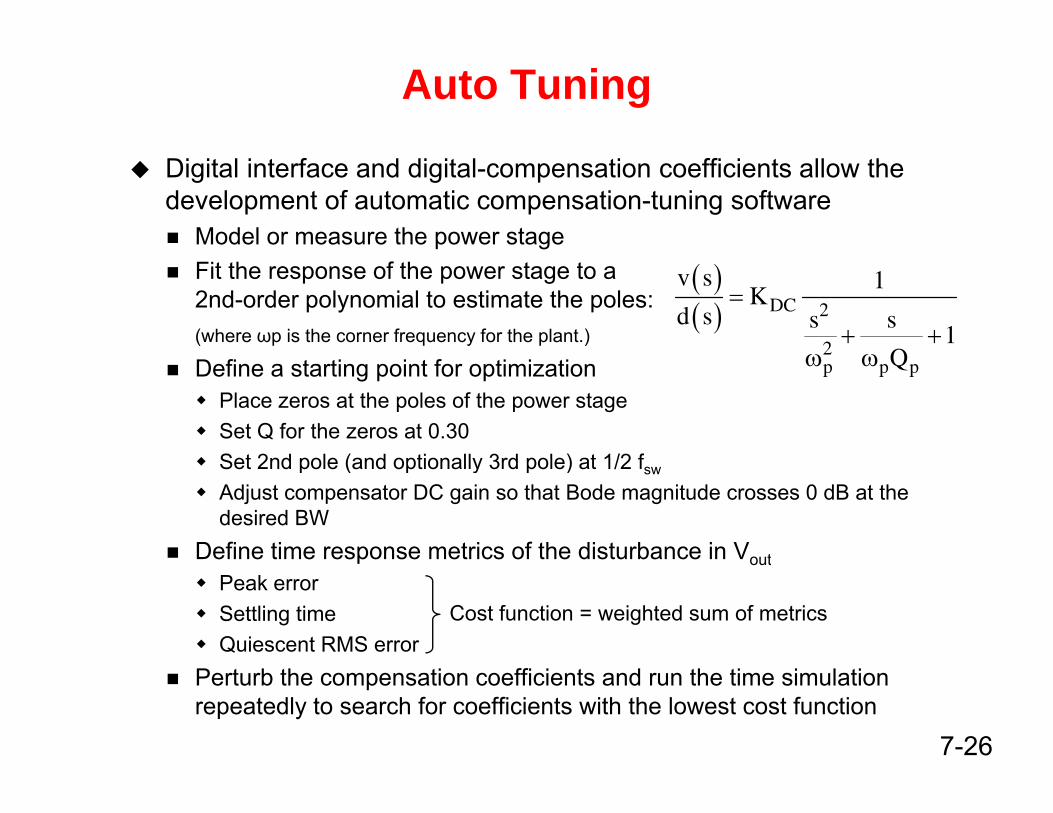
Digital interface and digital-compensation coefficients allow the development of automatic compensation-tuning software
Model or measure the power stageFit the response of the power stage to a 2nd-order polynomial to estimate the poles:(where ωp is the corner frequency for the plant.)
( )( ) DC 2
2
v s 1K
d s s s1
Q
=+ +
ω ωDefine a starting point for optimizationPlace zeros at the poles of the power stageSet Q for the zeros at 0.30Set 2nd pole (and optionally 3rd pole) at 1/2 f
p p pQω ω
Set 2nd pole (and optionally 3rd pole) at 1/2 fsw
Adjust compensator DC gain so that Bode magnitude crosses 0 dB at the desired BW
Define time response metrics of the disturbance in Voutp outPeak errorSettling timeQuiescent RMS error
Cost function = weighted sum of metrics
7-26
Perturb the compensation coefficients and run the time simulation repeatedly to search for coefficients with the lowest cost function
Auto Tuning
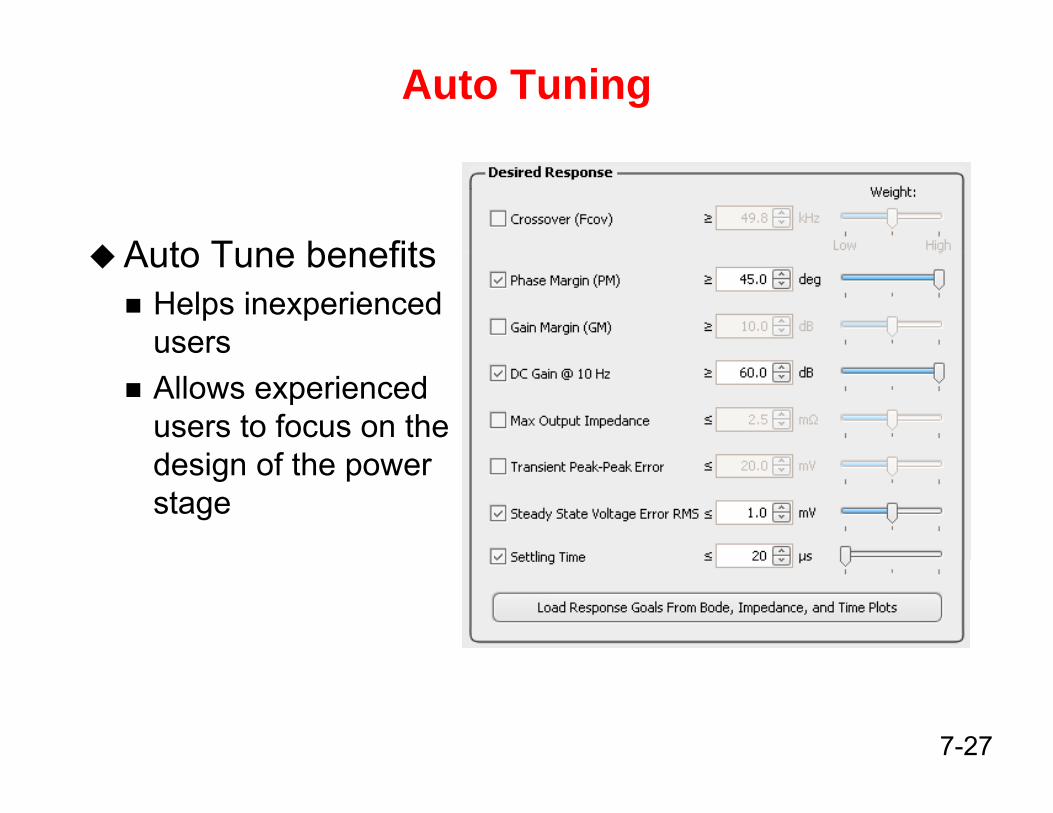
Auto Tune benefitsAuto Tune benefitsHelps inexperienced usersAllows experienced users to focus on the d i f thdesign of the power stage
7-27
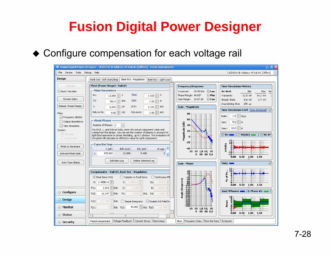
Fusion Digital Power Designer
Configure compensation for each voltage rail
7-28
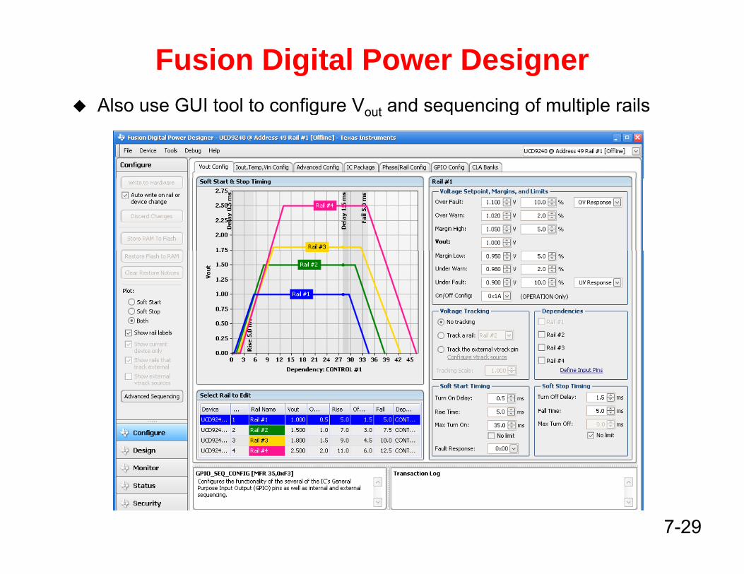
Fusion Digital Power Designer Also use GUI tool to configure V and sequencing of multiple railsAlso use GUI tool to configure Vout and sequencing of multiple rails
7-29
Conclusions
Digital control allows:Easy configuration of setpoint reference and loop compensation
Multiple configurations with one controller device
Automatically Identify loop-transfer function without external test equipmentequipment
Voltage and current monitoring
MarginingMargining
Digital controllers such as the UCD91xx, UCD92xx, and other PMBus-compliant controllers are easily configured using the Fusion Digital Power Designer program
Program does all the math for you!
7-30