Embed Size (px)
Citation preview
Topics covered:CPU Architecture
CSE 243: Introduction to Computer Architecture and Hardware/Software Interface
2
Arithmetic Logic Unit (ALU)
ALU is a purely combinatorial device: It has no memory or internal storage.
It has 2 input vectors: These may be called the A- and B-vector or the R- and S-
vector The inputs are as wide as the registers/system bus (e.g.,
16, 32 bits) It has 1 output vector
Usually denoted F

3
Arithmetic Logic Unit (ALU) (contd..)
Sample functions performed by the ALU
•F = A+B F = A+B+1
•F = A-B F = A-B-1
•F = A and B F = A or B
•F = not A F = not B
•F = not A + 1 F = not B + 1
•F = (not A) and B F = A and (not B)
•F = A xor B F = not (A xor B)
•F = A F = B
4
Arithmetic Logic Unit (ALU) (contd..)
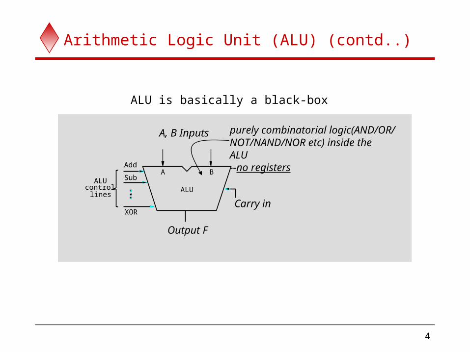
ALU is basically a black-box
ALU
Add
XOR
SubcontrolALU
lines
A B
A, B Inputs
Output F
purely combinatorial logic(AND/OR/NOT/NAND/NOR etc) inside theALU--no registers
Carry in
5
Arithmetic and Logic Unit (ALU) (contd..)
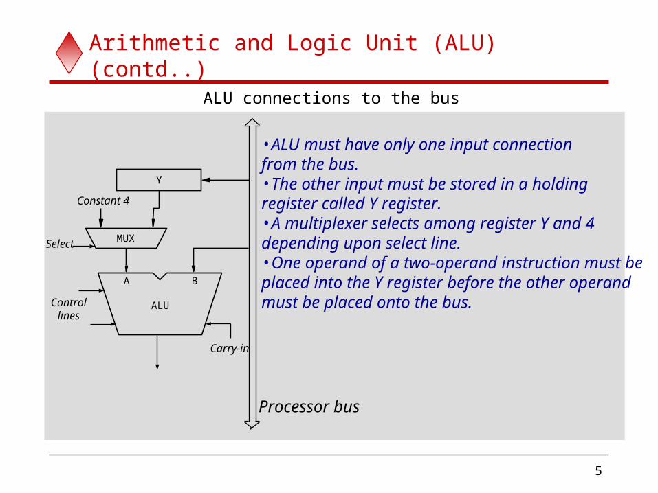
ALU connections to the bus
Y
ALU
A B
MUX
Constant 4
•ALU must have only one input connectionfrom the bus.•The other input must be stored in a holdingregister called Y register.•A multiplexer selects among register Y and 4depending upon select line.•One operand of a two-operand instruction must be placed into the Y register before the other operandmust be placed onto the bus.
Select
Controllines
Carry-in
Processor bus
6
Arithmetic and Logic Unit (ALU) (contd..)
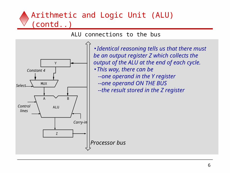
ALU connections to the bus
Y
ALU
A B
MUX
Constant 4
Select
Controllines
Carry-in
Processor bus
Z
•Identical reasoning tells us that there mustbe an output register Z which collects the output of the ALU at the end of each cycle.•This way, there can be --one operand in the Y register --one operand ON THE BUS --the result stored in the Z register
7
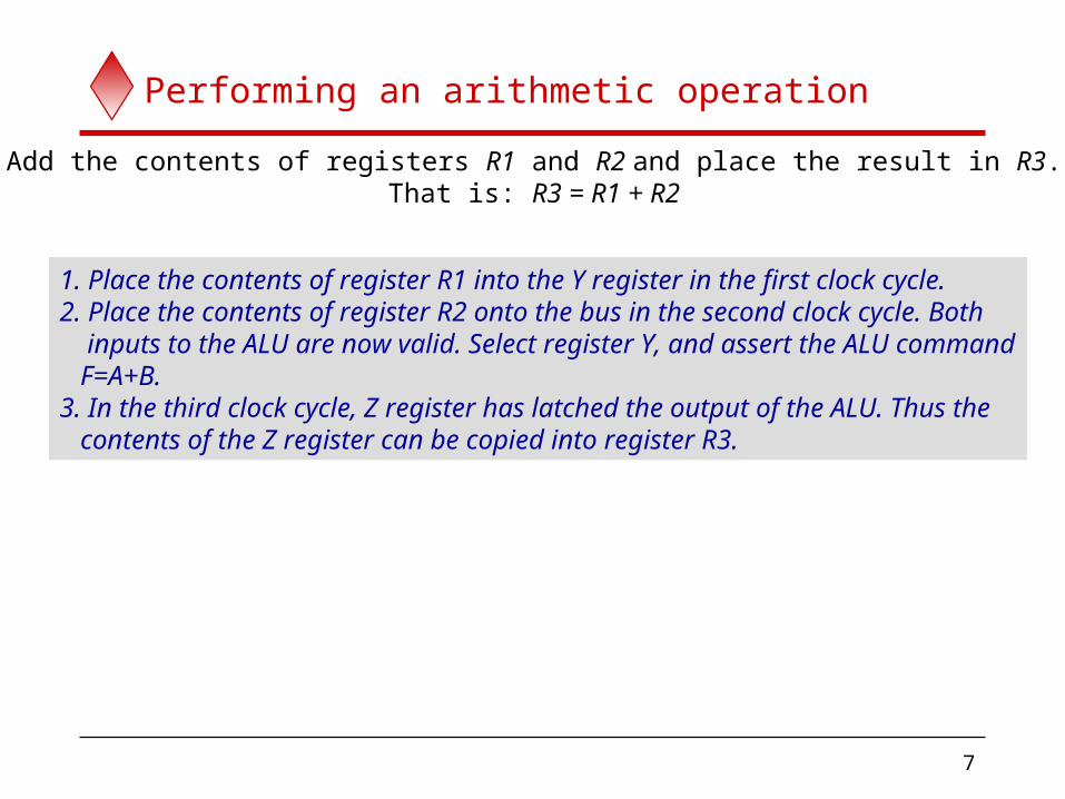
Performing an arithmetic operation
Add the contents of registers R1 and R2 and place the result in R3.That is: R3 = R1 + R2
1. Place the contents of register R1 into the Y register in the first clock cycle. 2. Place the contents of register R2 onto the bus in the second clock cycle. Both inputs to the ALU are now valid. Select register Y, and assert the ALU command F=A+B. 3. In the third clock cycle, Z register has latched the output of the ALU. Thus the contents of the Z register can be copied into register R3.
8
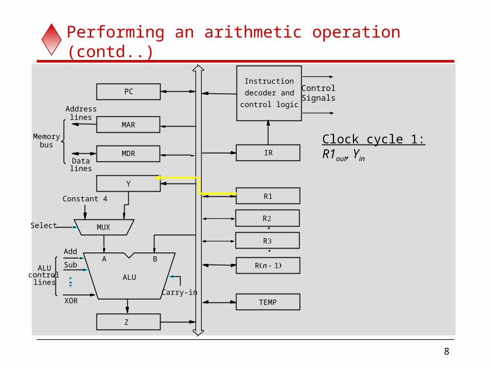
Performing an arithmetic operation (contd..)
IR
TEMP
R1
R n 1-( )
Z
busMemory
Addresslines
MAR
linesData
MDR
PC
Carry-in
Y
ALU
Add
XOR
SubcontrolALU
lines
A B
MUXSelect
Constant 4
Instruction
decoder and
control logic
ControlSignals
Clock cycle 1:R1out, Yin
R2
R3
9
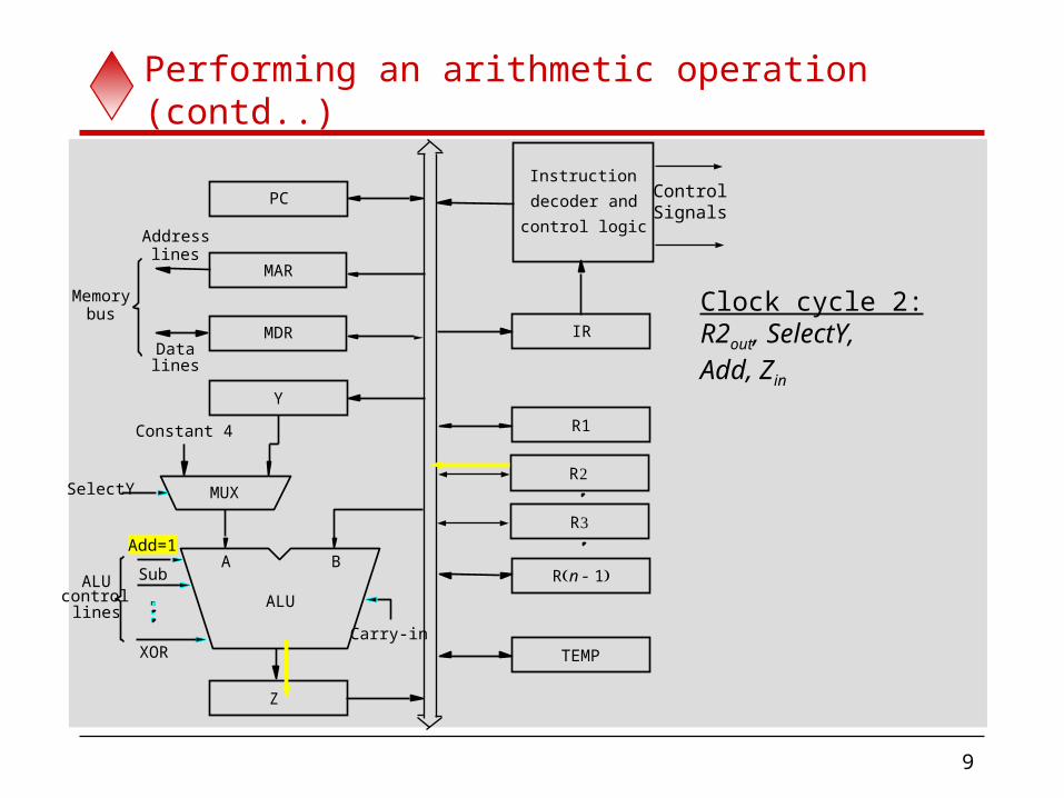
Performing an arithmetic operation (contd..)
IR
TEMP
R1
R n 1-( )
Z
busMemory
Addresslines
MAR
linesData
MDR
PC
Carry-in
Y
ALU
Add=1
XOR
SubcontrolALU
lines
A B
MUXSelectY
Constant 4
Instruction
decoder and
control logic
ControlSignals
Clock cycle 2:R2out, SelectY, Add, Zin
R2
R3
10
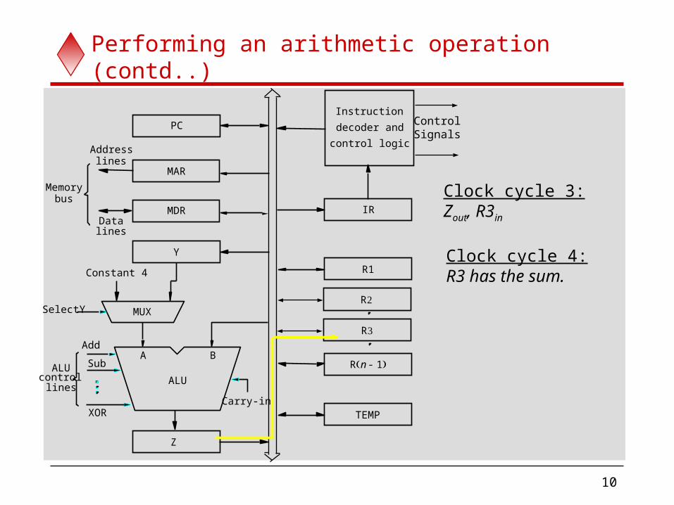
Performing an arithmetic operation (contd..)
IR
TEMP
R1
R n 1-( )
Z
busMemory
Addresslines
MAR
linesData
MDR
PC
Carry-in
Y
ALU
Add
XOR
SubcontrolALU
lines
A B
MUXSelectY
Constant 4
Instruction
decoder and
control logic
ControlSignals
Clock cycle 3:Zout, R3in
R2
R3
Clock cycle 4:R3 has the sum.
11
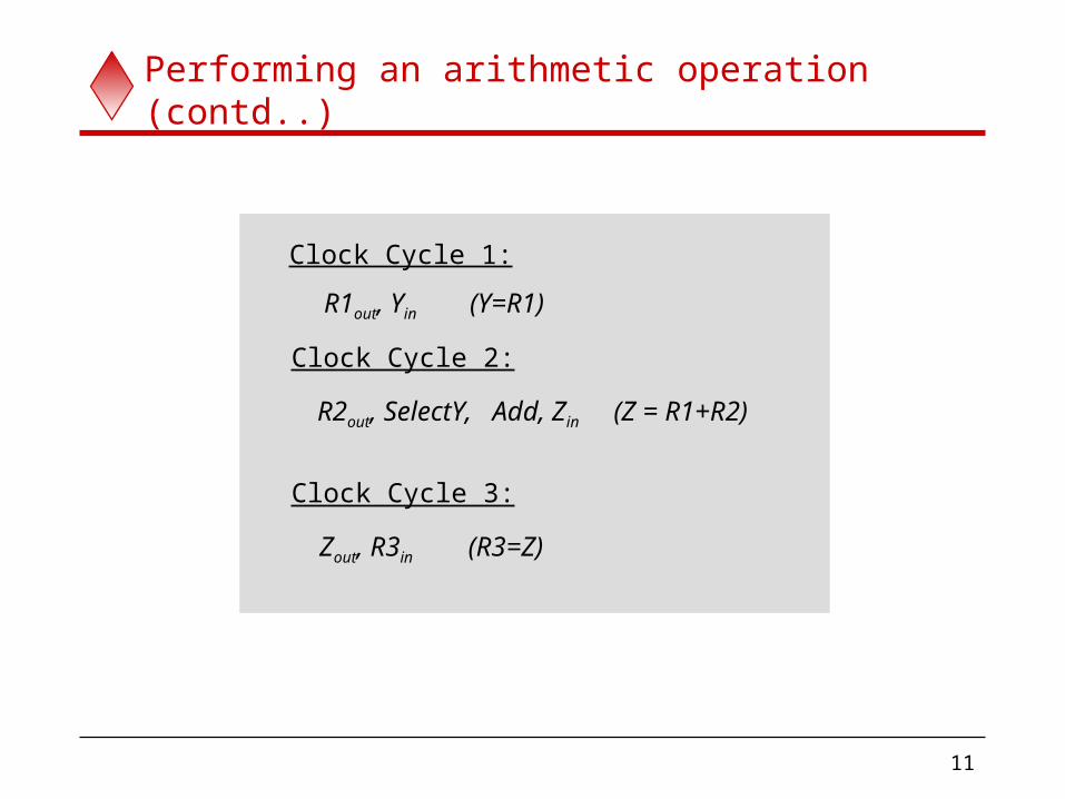
Performing an arithmetic operation (contd..)
Clock Cycle 1:
R1out, Yin (Y=R1)
Clock Cycle 2:
R2out, SelectY, Add, Zin (Z = R1+R2)
Clock Cycle 3:
Zout, R3in (R3=Z)
12
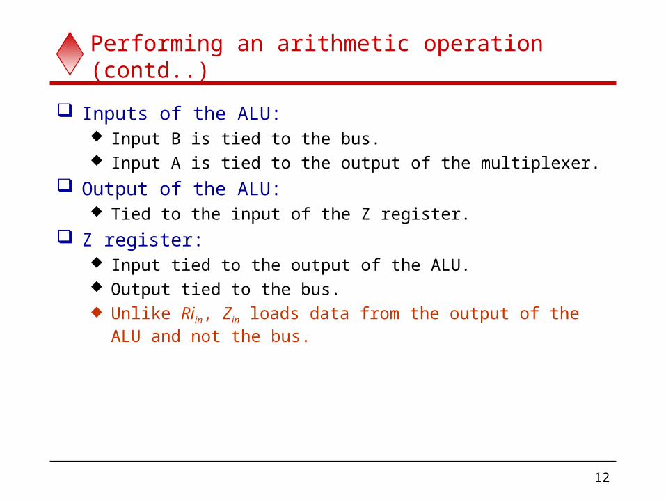
Performing an arithmetic operation (contd..)
Inputs of the ALU: Input B is tied to the bus. Input A is tied to the output of the multiplexer.
Output of the ALU: Tied to the input of the Z register.
Z register: Input tied to the output of the ALU. Output tied to the bus. Unlike Riin, Zin loads data from the output of the ALU and not
the bus.
13
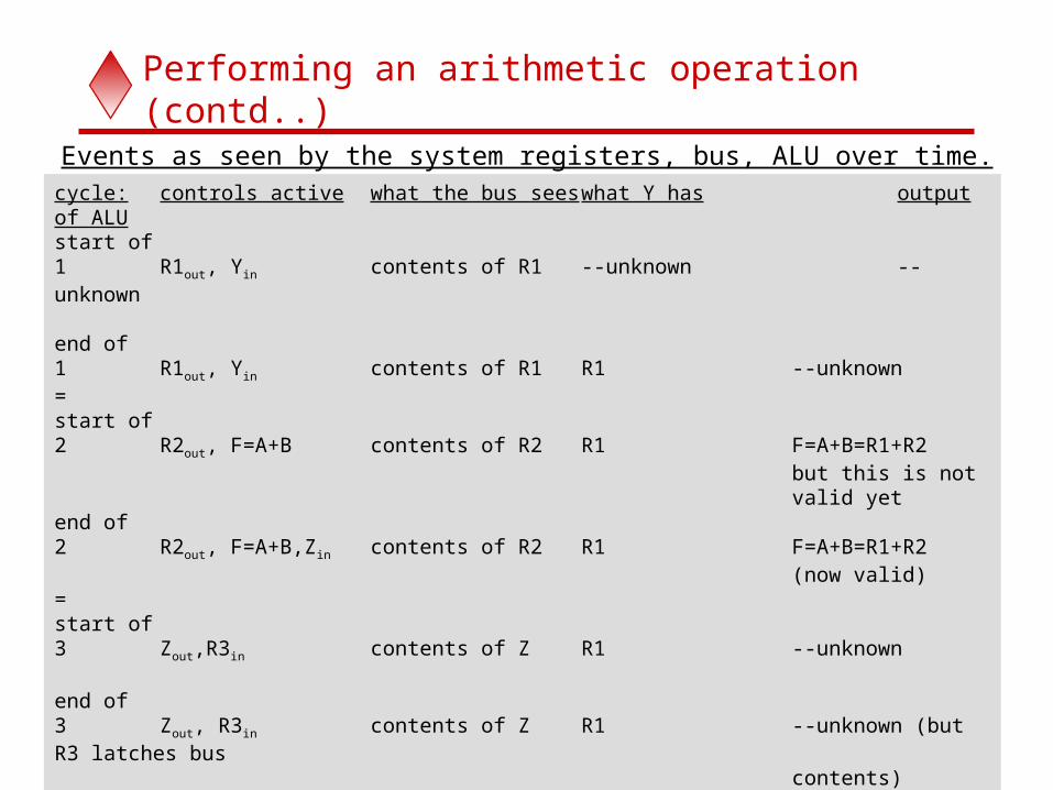
Performing an arithmetic operation (contd..)
Events as seen by the system registers, bus, ALU over time.cycle: controls active what the bus sees what Y has output of ALUstart of1 R1out, Yin contents of R1 --unknown --unknown
end of1 R1out, Yin contents of R1 R1 --unknown=start of2 R2out, F=A+B contents of R2 R1 F=A+B=R1+R2
but this is notvalid yet
end of2 R2out, F=A+B,Zin contents of R2 R1 F=A+B=R1+R2
(now valid)=start of 3 Zout,R3in contents of Z R1 --unknown
end of3 Zout, R3in contents of Z R1 --unknown (but R3 latches bus
contents)
14
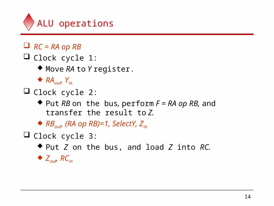
ALU operations
RC = RA op RB Clock cycle 1:
Move RA to Y register. RAout, Yin
Clock cycle 2: Put RB on the bus, perform F = RA op RB, and transfer
the result to Z. RBout, (RA op RB)=1, SelectY, Zin
Clock cycle 3: Put Z on the bus, and load Z into RC. Zout, RCin
15
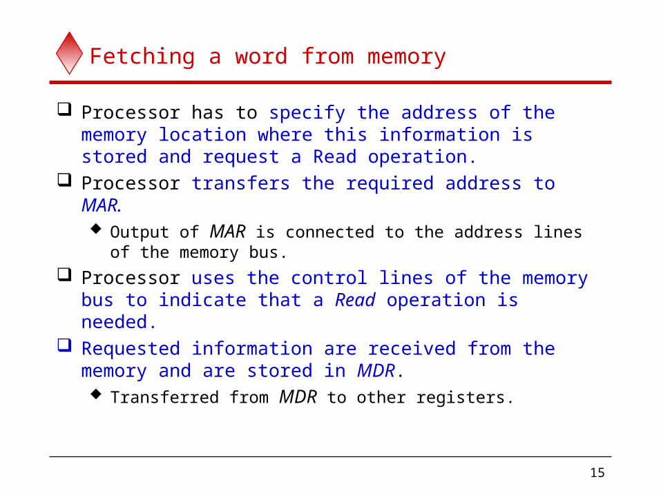
Fetching a word from memory
Processor has to specify the address of the memory location where this information is stored and request a Read operation.
Processor transfers the required address to MAR. Output of MAR is connected to the address lines of the
memory bus. Processor uses the control lines of the memory bus to
indicate that a Read operation is needed. Requested information are received from the memory
and are stored in MDR. Transferred from MDR to other registers.

16
Fetching a word from memory (contd..)
Connections for register MDR
MDR
Memory-busdata lines busMDRoutMDRoutE
MDR inMDR inE
MDRout and MDRin controlconnection to internal bus.
MDRoutE and MDRinE controlconnection to external bus.
17
Fetching a word from memory (contd..)
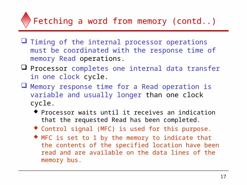
Timing of the internal processor operations must be coordinated with the response time of memory Read operations.
Processor completes one internal data transfer in one clock cycle.
Memory response time for a Read operation is variable and usually longer than one clock cycle. Processor waits until it receives an indication that the
requested Read has been completed. Control signal (MFC) is used for this purpose. MFC is set to 1 by the memory to indicate that the
contents of the specified location have been read and are available on the data lines of the memory bus.
18
Fetching a word from memory (contd..)
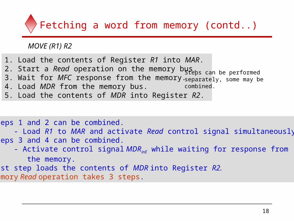
MOVE (R1) R2
1. Load the contents of Register R1 into MAR.2. Start a Read operation on the memory bus. 3. Wait for MFC response from the memory.4. Load MDR from the memory bus.5. Load the contents of MDR into Register R2.
Steps can be performedseparately, some may be combined.
Steps 1 and 2 can be combined. - Load R1 to MAR and activate Read control signal simultaneously.Steps 3 and 4 can be combined. - Activate control signal MDRinE while waiting for response from the memory.Last step loads the contents of MDR into Register R2.Memory Read operation takes 3 steps.
19
Fetching a word from memory (contd..)
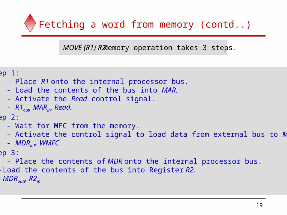
MOVE (R1) R2: Memory operation takes 3 steps.
Step 1: - Place R1 onto the internal processor bus. - Load the contents of the bus into MAR. - Activate the Read control signal. - R1out, MARin, Read. Step 2: - Wait for MFC from the memory. - Activate the control signal to load data from external bus to MDR. - MDRinE, WMFCStep 3: - Place the contents of MDR onto the internal processor bus. - Load the contents of the bus into Register R2. - MDRoutI, R2in
20
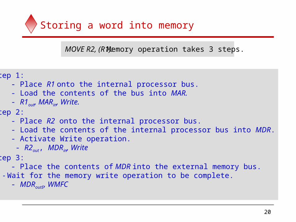
Storing a word into memory
MOVE R2, (R1):Memory operation takes 3 steps.
Step 1: - Place R1 onto the internal processor bus. - Load the contents of the bus into MAR. - R1out, MARin, Write. Step 2: - Place R2 onto the internal processor bus. - Load the contents of the internal processor bus into MDR. - Activate Write operation.. - R2out, MDRin, WriteStep 3: - Place the contents of MDR into the external memory bus. - Wait for the memory write operation to be complete. - MDRoutE, WMFC

21
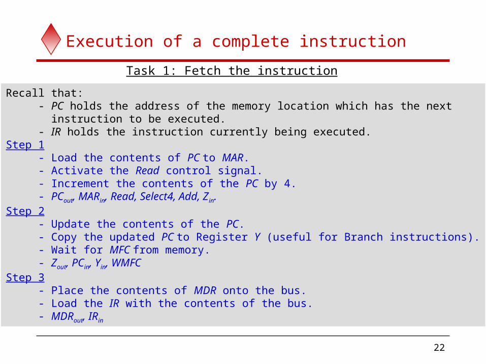
Execution of a complete instruction
Add the contents of a memory location pointed to by Register R3 to register R1. ADD (R3) R1
To execute the instruction we must execute the following tasks:1. Fetch the instruction.2. Fetch the operand (contents of the memory location pointed to by R3.)3. Perform the addition.4. Load the result into R1.
22
Execution of a complete instruction
Task 1: Fetch the instruction
Recall that: - PC holds the address of the memory location which has the next instruction to be executed. - IR holds the instruction currently being executed. Step 1 - Load the contents of PC to MAR. - Activate the Read control signal. - Increment the contents of the PC by 4. - PCout, MARin, Read, Select4, Add, Zin.Step 2 - Update the contents of the PC. - Copy the updated PC to Register Y (useful for Branch instructions). - Wait for MFC from memory. - Zout, PCin, Yin, WMFCStep 3 - Place the contents of MDR onto the bus. - Load the IR with the contents of the bus. - MDRout, IRin
23
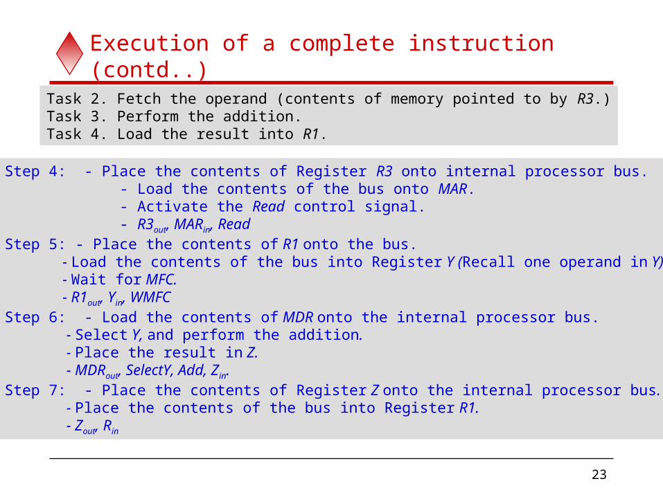
Execution of a complete instruction (contd..)
Task 2. Fetch the operand (contents of memory pointed to by R3.)Task 3. Perform the addition.Task 4. Load the result into R1.
Step 4: - Place the contents of Register R3 onto internal processor bus. - Load the contents of the bus onto MAR. - Activate the Read control signal. - R3out, MARin, ReadStep 5: - Place the contents of R1 onto the bus. - Load the contents of the bus into Register Y (Recall one operand in Y). - Wait for MFC. - R1out, Yin, WMFCStep 6: - Load the contents of MDR onto the internal processor bus. - Select Y, and perform the addition. - Place the result in Z. - MDRout, SelectY, Add, Zin.Step 7: - Place the contents of Register Z onto the internal processor bus. - Place the contents of the bus into Register R1. - Zout, Rin
24
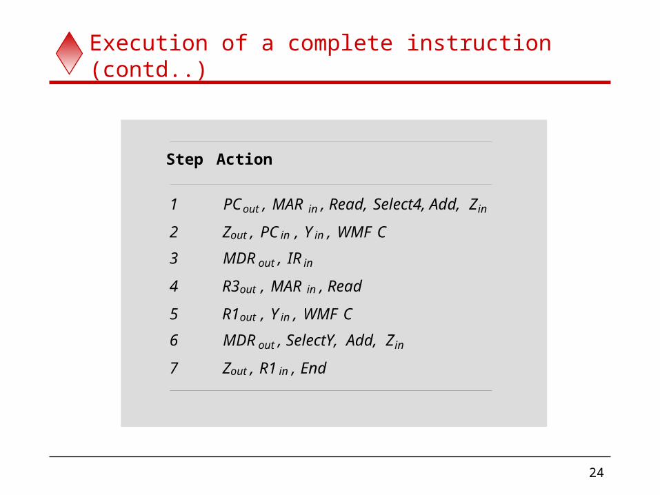
Execution of a complete instruction (contd..)
Step Action
1 PCout , MAR in ,Read,Select4,Add, Zin
2 Zout , PCin , Y in , WMFC
3 MDRout , IR in
4 R3out , MAR in ,Read
5 R1out , Y in , WMF C
6 MDRout ,SelectY,Add, Zin
7 Zout , R1in , End
25
Branch instructions
Recall that the updated contents of the PC are copied into Register Y in Step 2. Not necessary for ADD instruction, but useful in BRANCH
instructions.: Branch target address is computed by adding the updated
contents of the PC to an offset. Copying the updated contents of the PC to Register Y
speeds up the execution of BRANCH instruction. Since the Fetch cycle is the same for all instructions,
this step is performed for all instructions. Since Register Y is not used for any other purpose at that
time it does not have any impact on the execution of the instruction.