Embed Size (px)
Citation preview

User's GuideSLVU888–April 2013
TPS54628EVM-052, 6-A, Regulator Evaluation Module
This user's guide contains information for the TPS54628EVM-052 evaluation module (EVM) as well as forthe TPS54628. Included are the performance specifications, schematic, and the bill of materials of theTPS54628EVM-052.
Contents1 Introduction .................................................................................................................. 32 Performance Specification Summary ..................................................................................... 33 Modifications ................................................................................................................. 3
3.1 Output Voltage Setpoint ........................................................................................... 33.2 Output Filter and Closed-Loop Response ...................................................................... 4
4 Test Setup and Results .................................................................................................... 44.1 Input/Output Connections ......................................................................................... 44.2 Start-Up Procedure ................................................................................................ 54.3 Efficiency ............................................................................................................ 54.4 Load Regulation .................................................................................................... 64.5 Line Regulation ..................................................................................................... 74.6 Load Transient Response ........................................................................................ 74.7 Output Voltage Ripple ............................................................................................. 84.8 Input Voltage Ripple ............................................................................................... 94.9 Start-Up ............................................................................................................ 104.10 Shut-Down ......................................................................................................... 11
5 Board Layout ............................................................................................................... 125.1 Layout .............................................................................................................. 12
6 Schematic, Bill of Materials, and Reference ........................................................................... 156.1 Schematic ......................................................................................................... 156.2 Bill of Materials .................................................................................................... 166.3 Reference .......................................................................................................... 16
List of Figures
1 TPS54628EVM-052 Efficiency ............................................................................................ 5
2 TPS54628EVM-052 Light-Load Efficiency............................................................................... 6
3 TPS54628EVM-052 Load Regulation, VIN = 5 V and VIN = 12 V. ..................................................... 6
4 TPS54628EVM-052 Line Regulation ..................................................................................... 7
5 TPS54628EVM-052 Load Transient Response......................................................................... 7
6 TPS54628EVM-052 Output Voltage Ripple (IOUT = 6 A) ............................................................... 8
7 TPS54628EVM-052 Output Voltage Ripple (IOUT = 300 mA) .......................................................... 8
8 TPS54628EVM-052 Output Voltage Ripple (IOUT = 0.2 mA) ........................................................... 9
9 TPS54628EVM-052 Input Voltage Ripple ............................................................................... 9
10 TPS54628EVM-052 Start-Up Relative to VIN with SS ................................................................ 10
11 TPS54628EVM-052 Start-Up Relative to EN with SS ................................................................ 10
12 TPS54628EVM-052 Shut-Down Relative to VIN with SS ............................................................. 11
13 TPS54628EVM-052 Shut-Down Relative to EN with SS............................................................. 11
14 Top Assembly .............................................................................................................. 12
D-CAP2, Eco-mode are trademarks of Texas Instruments.
1SLVU888–April 2013 TPS54628EVM-052, 6-A, Regulator Evaluation ModuleSubmit Documentation Feedback
Copyright © 2013, Texas Instruments Incorporated

www.ti.com
15 Top Layer................................................................................................................... 13
16 Internal Layer 1 ............................................................................................................ 13
17 Internal Layer 2 ............................................................................................................ 14
18 Bottom Layer ............................................................................................................... 14
19 TPS54628EVM-052 Schematic Diagram............................................................................... 15
List of Tables
1 Input Voltage and Output Current Summary ............................................................................ 3
2 TPS54628EVM-052 Performance Specifications Summary .......................................................... 3
3 Output Voltages and Recommended Component Values............................................................. 4
4 Connection and Test Points ............................................................................................... 4
5 Bill of Materials............................................................................................................. 16
2 TPS54628EVM-052, 6-A, Regulator Evaluation Module SLVU888–April 2013Submit Documentation Feedback
Copyright © 2013, Texas Instruments Incorporated

R1VO = 0.765 1+
R2
æ ö´ ç ÷
è ø
www.ti.com Introduction
1 Introduction
The TPS54628 is a single, adaptive on-time, D-CAP2™-mode, synchronous buck converter requiring alow external component count. The D-CAP2 control circuit is optimized for low-ESR output capacitorssuch as POSCAP, SP-CAP, or ceramic types and features fast-transient response with no externalcompensation. The switching frequency is internally set at a nominal 650 kHz. The high-side and low-sideswitching MOSFETs are incorporated inside the TPS54628 package along with the gate-drive circuitry.The low drain-to-source on-resistance of the MOSFETs allows the TPS54628 to achieve high efficienciesand helps keep the junction temperature low at high-output currents. To further enhance efficiency at lightloads, the TPS54628 features pulse skipping Eco-mode™ operation. The TPS54628 dc/dc synchronousconverter is designed to provide up to a 6-A output from an input voltage source of 4.5 V to 18 V. Theoutput voltage range is from 0.76 V to 5.5 V. Rated input voltage and output current range for theevaluation module are given in Table 1.
The TPS54628EVM-052 evaluation module circuit is a single, synchronous buck converter providing1.05 V at 6 A from 4.5-V to 18-V input. This user’s guide describes the TPS54628EVM-052 performance.
Table 1. Input Voltage and Output Current Summary
EVM Input Voltage Range Output Current Range
TPS54628EVM-052 VIN = 4.5 V to 18 V 0 A to 6 A
2 Performance Specification Summary
A summary of the TPS54628EVM-052 performance specifications is provided in Table 2. Specificationsare given for an input voltage of VIN = 12 V and an output voltage of 1.05 V, unless otherwise noted. Theambient temperature is 25°C for all measurement, unless otherwise noted.
Table 2. TPS54628EVM-052 Performance Specifications Summary
Specifications Test Conditions Min Typ Max Unit
Input voltage range (VIN) 4.5 12 18 V
Output voltage 1.05 V
Operating frequency VIN = 12 V, IO = 1 A 650 kHz
Output current range 0 6 A
Line regulation IO = 3 A ±0.3 %
VIN = 12 V +0.90, %Load regulation –0.14
Overcurrent limit VIN = 12 V, LO = 1.5 µH 6.7 7.3 8.9 A
Output ripple voltage VIN = 12 V, IO = 6 A 15 mVPP
Maximum efficiency VIN = 5 V, IO= 0.9 A 88.6 %
3 Modifications
These evaluation modules are designed to provide access to the features of the TPS54628. Somemodifications can be made to this module.
3.1 Output Voltage Setpoint
To change the output voltage of the EVMs, it is necessary to change the value of resistor R1. Changingthe value of R1 can change the output voltage above 0.765 V. The value of R1 for a specific outputvoltage can be calculated using Equation 1.
For output voltage from 0.76 V to 5.5 V:
(1)
3SLVU888–April 2013 TPS54628EVM-052, 6-A, Regulator Evaluation ModuleSubmit Documentation Feedback
Copyright © 2013, Texas Instruments Incorporated

Test Setup and Results www.ti.com
Table 3 lists the R1 values for some common output voltages. A feed forward capacitor (C4) may be usedto improve phase margin. Feed forward capacitors are most effective for higher output voltages of 1.8 V orabove. Pads for this component (C4) are provided on the printed-circuit board (PCB). Note that theresistor values given in Table 3 are standard values and not the exact value calculated using Equation 1.
Table 3. Output Voltages and Recommended Component Values
C9 + C10 +C11Output C4 (pF) (1) L1 (µH)R1 R2 (µF)Voltage (kΩ) (kΩ)(V) MIN TYP MAX MIN TYP MAX MIN MAX
1 6.81 22.1 5 150 220 1.0 1.5 4.7 22 68
1.05 8.25 22.1 5 150 220 1.0 1.5 4.7 22 68
1.2 12.7 22.1 5 100 1.0 1.5 4.7 22 68
1.5 21.5 22.1 5 68 1.0 1.5 4.7 22 68
1.8 30.1 22.1 5 22 1.2 1.5 4.7 22 68
2.5 49.9 22.1 5 22 1.5 2.2 4.7 22 68
3.3 73.2 22.1 2 22 1.8 2.2 4.7 22 68
5 124 22.1 2 22 2.2 3.3 4.7 22 68(1) Optional
3.2 Output Filter and Closed-Loop Response
The TPS54628 relies on the output filter characteristics to ensure stability of the control loop. Therecommended output filter components for common output voltages are given in Table 3. It may bepossible for other output filter component values to provide acceptable closed-loop characteristics. R3 andTP4 are provided for convenience in breaking the control loop and measuring the closed-loop response.
4 Test Setup and Results
This section describes how to properly connect, set up, and use the TPS54628EVM-052. The section alsoincludes test results typical for the evaluation modules and efficiency, output load regulation, output lineregulation, load-transient response, output voltage ripple, input voltage ripple, start-up, and switchingfrequency.
4.1 Input/Output Connections
The TPS54628EVM-052 is provided with input and output connectors and test points as shown in Table 4.A power supply capable of supplying 3 A must be connected to J1 through a pair of 20-AWG wires. Theload must be connected to J2 through a pair of 20-AWG wires. The maximum load current capability is6 A. Wire lengths must be minimized to reduce losses in the wires. Test point TP1 provides a place tomonitor the VIN input voltages with TP2 providing a convenient ground reference. TP8 is used to monitorthe output voltage with TP9 as the ground reference.
Table 4. Connection and Test Points
Reference Designator Function
J1 VIN (see Table 1 for VIN range)
J2 VOUT, 1.05 V at 6-A maximum
JP1 EN control. Connect EN to OFF to disable, connect EN to ON to enable
TP1 VIN test point at VIN connector
TP2 GND test point at VIN connector
TP3 EN test point
TP4 Loop response measurement test point
TP5 VREG5 test point
TP6 Switch node test point
TP7 Analog ground test point
4 TPS54628EVM-052, 6-A, Regulator Evaluation Module SLVU888–April 2013Submit Documentation Feedback
Copyright © 2013, Texas Instruments Incorporated

0
10
20
30
40
50
60
70
80
90
100
0 0.5 1 1.5 2 2.5 3 3.5 4 4.5 5 5.5 6
Effi
cien
cy -
%
Output Current - A
C001
VIN = 5 V VIN = 12 V
www.ti.com Test Setup and Results
Table 4. Connection and Test Points (continued)
Reference Designator Function
TP8 Output voltage test point at VOUT connector
TP9 Ground test point at VOUT connector
4.2 Start-Up Procedure1. Ensure that the jumper at JP1 (Enable control) is set from EN to OFF.
2. Apply appropriate VIN voltage to VIN and PGND terminals at J1.
3. Move the jumper at JP1 (Enable control) to cover EN and ON. The EVM enables the output voltage.
4.3 Efficiency
Figure 1 shows the efficiency for the TPS54628EVM-052 at an ambient temperature of 25°C.
Figure 1. TPS54628EVM-052 Efficiency
5SLVU888–April 2013 TPS54628EVM-052, 6-A, Regulator Evaluation ModuleSubmit Documentation Feedback
Copyright © 2013, Texas Instruments Incorporated

-1
-0.8
-0.6
-0.4
-0.2
0
0.2
0.4
0.6
0.8
1
0 0.5 1 1.5 2 2.5 3 3.5 4 4.5 5 5.5 6
Load
Reg
ulat
ion
- %
Output Current - A
C003
VIN = 5 V
VIN = 12 V
0
10
20
30
40
50
60
70
80
90
100
0.001 0.01 0.1 1 10
Effi
cien
cy -
%
Output Current - A
C002
VIN = 5 V
VIN = 12 V
Test Setup and Results www.ti.com
Figure 2 shows the efficiency at light loads for the TPS54628EVM-052 at an ambient temperature of 25°C.
Figure 2. TPS54628EVM-052 Light-Load Efficiency
4.4 Load Regulation
The load regulation for the TPS54628EVM-052 is shown in Figure 3.
Figure 3. TPS54628EVM-052 Load Regulation, VIN = 5 V and VIN = 12 V.
6 TPS54628EVM-052, 6-A, Regulator Evaluation Module SLVU888–April 2013Submit Documentation Feedback
Copyright © 2013, Texas Instruments Incorporated

V = 20 mV / div (ac coupled)OUT
Time = 200 µsec / div
I = 2 A / divOUT
Load step = 1.5 - 4.5 A, slew rate = 500 mA / µsec
-0.5
-0.4
-0.3
-0.2
-0.1
0
0.1
0.2
0.3
0.4
0.5
4 6 8 10 12 14 16 18
Line
Rgu
latio
n -
%
Input Voltage - V
C004
IOUT = 3 A
www.ti.com Test Setup and Results
4.5 Line Regulation
The line regulation for the TPS54628EVM-052 is shown in Figure 4.
Figure 4. TPS54628EVM-052 Line Regulation
4.6 Load Transient Response
The TPS54628EVM-052 response to load transient is shown in Figure 5. The current step is from 1.5 A to4.5 A. Total peak-to-peak voltage variation is as shown.
Figure 5. TPS54628EVM-052 Load Transient Response
7SLVU888–April 2013 TPS54628EVM-052, 6-A, Regulator Evaluation ModuleSubmit Documentation Feedback
Copyright © 2013, Texas Instruments Incorporated
V = 20 mV / div (ac coupled)OUT
Time = 1 µsec / div
SW = 5 V / div
V = 20 mV / div (ac coupled)OUT
Time = 1 µsec / div
SW = 5 V / div
Test Setup and Results www.ti.com
4.7 Output Voltage Ripple
The TPS54628EVM-052 output voltage ripple is shown in Figure 6. The output current is the rated full loadof 6 A.
Figure 6. TPS54628EVM-052 Output Voltage Ripple (IOUT = 6 A)
The TPS54628EVM-052 output voltage ripple is shown in Figure 7. The output current is 300 mA.
Figure 7. TPS54628EVM-052 Output Voltage Ripple (IOUT = 300 mA)
8 TPS54628EVM-052, 6-A, Regulator Evaluation Module SLVU888–April 2013Submit Documentation Feedback
Copyright © 2013, Texas Instruments Incorporated

V = 100 mV / div (ac coupled)IN
Time = 1 µsec / div
SW = 5 V / div
V = 20 mV / div (ac coupled)OUT
Time = 2 msec / div
SW = 5 V / div
www.ti.com Test Setup and Results
The TPS54628EVM-052 output voltage ripple is shown in Figure 8. The output current is 0.2 mA.
Figure 8. TPS54628EVM-052 Output Voltage Ripple (IOUT = 0.2 mA)
4.8 Input Voltage Ripple
The TPS54628EVM-052 input voltage ripple is shown in Figure 9. The output current is the rated full loadof 6 A.
Figure 9. TPS54628EVM-052 Input Voltage Ripple
9SLVU888–April 2013 TPS54628EVM-052, 6-A, Regulator Evaluation ModuleSubmit Documentation Feedback
Copyright © 2013, Texas Instruments Incorporated
V = 1 V / divOUT
Time = 2 msec / div
EN = 10 V / div
SS = 5 V / div
V = 10 V / divIN
V = 1 V / divOUT
Time = 2 msec / div
EN = 10 V / div
SS = 5 V / div
V = 10 V / divIN
Test Setup and Results www.ti.com
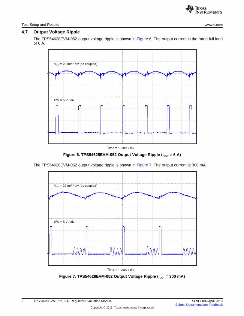
4.9 Start-Up
The TPS54628EVM-052 start-up waveforms relative to VIN and EN are shown in Figure 10 and Figure 11.RLOAD = 1 Ω.
Figure 10. TPS54628EVM-052 Start-Up Relative to VIN with SS
Figure 11. TPS54628EVM-052 Start-Up Relative to EN with SS
10 TPS54628EVM-052, 6-A, Regulator Evaluation Module SLVU888–April 2013Submit Documentation Feedback
Copyright © 2013, Texas Instruments Incorporated
V = 1 V / divOUT
Time = 2 msec / div
EN = 10 V / div
SS = 5 V / div
V = 10 V / divIN
V = 1 V / divOUT
Time = 2 msec / div
EN = 10 V / div
SS = 5 V / div
V = 10 V / divIN
www.ti.com Test Setup and Results
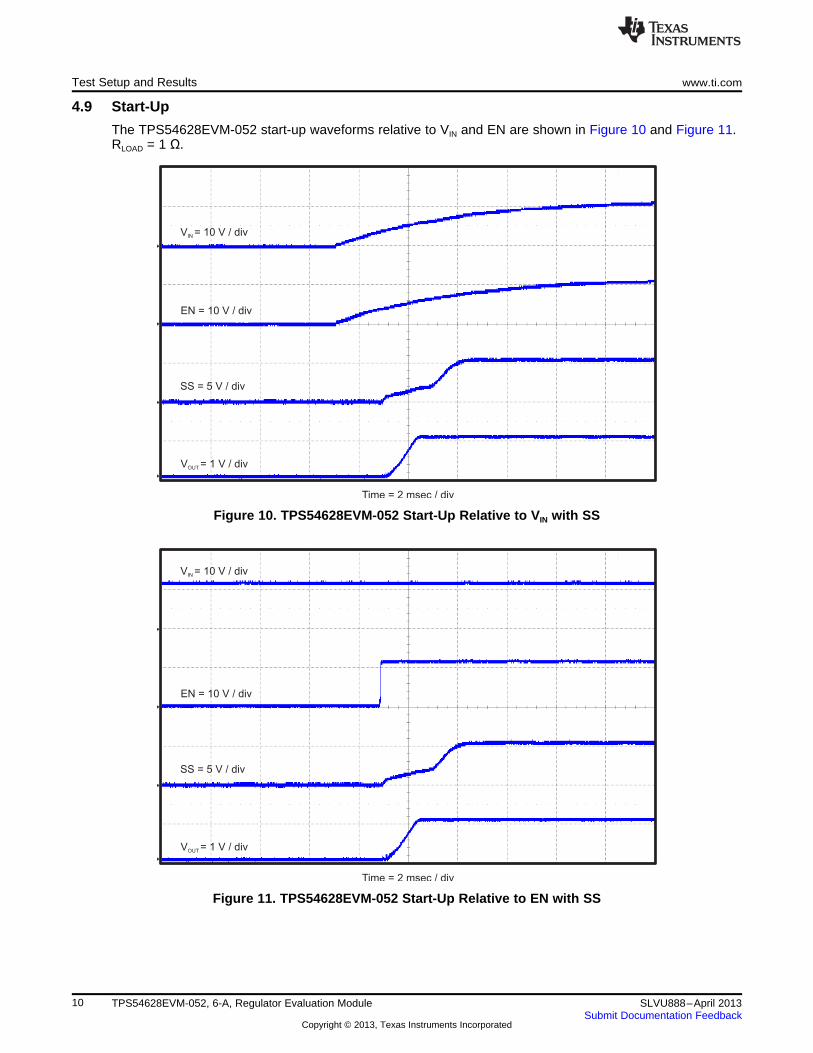
4.10 Shut-Down
The TPS54628EVM-052 shut-down waveforms relative to VIN and EN are shown in Figure 12 andFigure 13. RLOAD = 1 Ω.
Figure 12. TPS54628EVM-052 Shut-Down Relative to VIN with SS
Figure 13. TPS54628EVM-052 Shut-Down Relative to EN with SS
11SLVU888–April 2013 TPS54628EVM-052, 6-A, Regulator Evaluation ModuleSubmit Documentation Feedback
Copyright © 2013, Texas Instruments Incorporated

Board Layout www.ti.com
5 Board Layout
This section provides description of the TPS54628EVM-052, board layout, and layer illustrations.
5.1 Layout
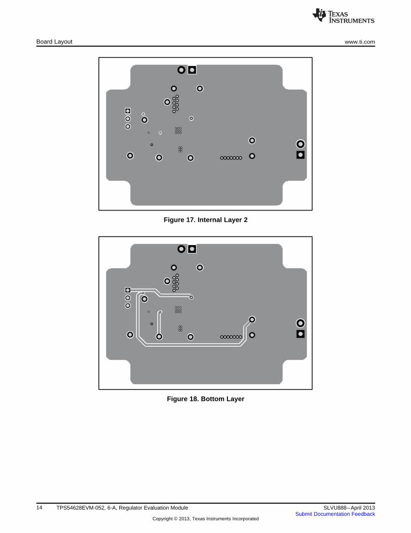
The board layout for the TPS54628EVM-052 is shown in Figure 14 through Figure 18. The top layercontains the main power traces for VIN, VOUT, and ground. Also on the top layer are connections for thepins of the TPS54628 and a large area filled with ground. Most of the signal traces also are located on thetop side. The input decoupling capacitors are located as close to the IC as possible. The input and outputconnectors, test points, and all of the components are located on the top side. An analog ground (GND)area is provided on the top side. Analog ground (GND) and power ground (PGND) are connected at asingle point on the top layer near C6. The two internal layers are completely dedicated to power groundplanes. The bottom layer is primarily power ground. Traces also connect VIN to the enable control jumper,VREG5 test points and the feedback trace from VOUT to the voltage setpoint divider network.
Figure 14. Top Assembly
12 TPS54628EVM-052, 6-A, Regulator Evaluation Module SLVU888–April 2013Submit Documentation Feedback
Copyright © 2013, Texas Instruments Incorporated

www.ti.com Board Layout
Figure 15. Top Layer
Figure 16. Internal Layer 1
13SLVU888–April 2013 TPS54628EVM-052, 6-A, Regulator Evaluation ModuleSubmit Documentation Feedback
Copyright © 2013, Texas Instruments Incorporated
Board Layout www.ti.com
Figure 17. Internal Layer 2
Figure 18. Bottom Layer
14 TPS54628EVM-052, 6-A, Regulator Evaluation Module SLVU888–April 2013Submit Documentation Feedback
Copyright © 2013, Texas Instruments Incorporated
OFF
EN
ON
Not Installed
GND
GND
VOUT
VIN
1
1
1
1
1
1
VIN = 4.5 V - 18 V
VOUT = 1.05 V, 6 A
R3 0TP4
R1 8.25k
C5
1uF
TP5
TP2
TP1
C6
8200pF R5
TP6
TP8
C4
TP3
C2
10uF
C8 C9
22uF
C10
22uF TP9
TP7
R2
22.1k
C7 0.1uFL1 1.5uH
D1
1
2
J1
1
2
3
JP1
C1
10uF
C3
0.1uF
R4 10.0k
1
2J2
C11
1EN
2VFB
3VREG5
4SS
5GND
6SW
7VBST
8VIN
9
PWPD
U1
TPS54628DDA
VOUT
VOUT
www.ti.com Schematic, Bill of Materials, and Reference
6 Schematic, Bill of Materials, and Reference
6.1 Schematic
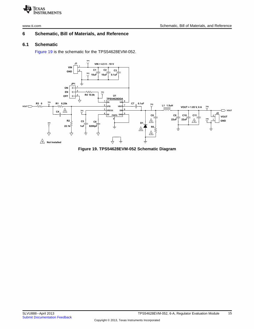
Figure 19 is the schematic for the TPS54628EVM-052.
Figure 19. TPS54628EVM-052 Schematic Diagram
15SLVU888–April 2013 TPS54628EVM-052, 6-A, Regulator Evaluation ModuleSubmit Documentation Feedback
Copyright © 2013, Texas Instruments Incorporated

Schematic, Bill of Materials, and Reference www.ti.com
6.2 Bill of Materials
Table 5. Bill of Materials
RefDes Qty Value Description Size Part Number MFR
C1, C2 2 10uF Capacitor, Ceramic, 25V, X5R, 20% 1210 Std Std
C3, C7 2 0.1uF Capacitor, Ceramic, 50V, X7R, 10% 0603 Std Std
C4, C8 0 Open Capacitor, Ceramic 0603 Std Std
C5 1 1uF Capacitor, Ceramic, 16V, X7R, 10% 0603 Std Std
C6 1 8200pF Capacitor, Ceramic, 25V, X7R , 10% 0603 Std Std
C9, C10 2 22uF Capacitor, Ceramic, 6.3V, X5R, 20% 1206 C3216X5R0J226M TDK
C11 1 Open Capacitor, Ceramic 1206 Std Std
D1 0 Open Diode, 0.5 A, 30 V, 2PIN TUMD2 RSX051VA-30 Rohm
J1, J2 2 ED555/2DS Terminal Block, 2-pin, 6-A, 3.5mm 0.27 x 0.25 inch ED555/2DS Sullins
JP1 1 PEC03SAAN Header, Male 3-pin, 100mil spacing 0.100 inch x 3 PEC03SAAN Sullins
L1 1 1.5uH Inductor, SMT, 11.6 A, 10.67 milliohm 0.256 x 0.280 inch SPM6530T-1R5M100 TDK
R1 1 8.25k Resistor, Chip, 1/16W, 1% 0603 Std Std
R2 1 22.1k Resistor, Chip, 1/16W, 1% 0603 Std Std
R3, R5 2 0 Resistor, Chip, 1/16W, 1% 0603 Std Std
R4 1 10.0k Resistor, Chip, 1/16W, 1% 0603 Std Std
R5 0 Open Resistor, Chip, 1/16W, 1% 0603 Std Std
TP1, TP3, 3 5000 Test Point, Red, Thru Hole Color Keyed 0.100 x 0.100 inch 5000 KeystoneTP4, TP5,TP6, TP8
TP2, TP7, 3 5001 Test Point, Black, Thru Hole Color Keyed 0.100 x 0.100 inch 5001 KeystoneTP9
U1 1 TPS54628DDA IC, 4.5-18 V Input, 6-A Sync. Step-Down Converter SO8[DDA] TPS54628DDA TIwith Eco-mode
– 1 Shunt, 100-mil, Black 0.100 929950-00 3M
– 1 PCB PWR056 Any
6.3 Reference1. TPS54628, 4.5 V to 18 V Input, 6-A Synchronous Step-Down Converter with Eco-mode™ data sheet
(SLVSBW5)
16 TPS54628EVM-052, 6-A, Regulator Evaluation Module SLVU888–April 2013Submit Documentation Feedback
Copyright © 2013, Texas Instruments Incorporated

EVALUATION BOARD/KIT/MODULE (EVM) ADDITIONAL TERMS
Texas Instruments (TI) provides the enclosed Evaluation Board/Kit/Module (EVM) under the following conditions:
The user assumes all responsibility and liability for proper and safe handling of the goods. Further, the user indemnifies TI from all claimsarising from the handling or use of the goods.
Should this evaluation board/kit not meet the specifications indicated in the User’s Guide, the board/kit may be returned within 30 days fromthe date of delivery for a full refund. THE FOREGOING LIMITED WARRANTY IS THE EXCLUSIVE WARRANTY MADE BY SELLER TOBUYER AND IS IN LIEU OF ALL OTHER WARRANTIES, EXPRESSED, IMPLIED, OR STATUTORY, INCLUDING ANY WARRANTY OFMERCHANTABILITY OR FITNESS FOR ANY PARTICULAR PURPOSE. EXCEPT TO THE EXTENT OF THE INDEMNITY SET FORTHABOVE, NEITHER PARTY SHALL BE LIABLE TO THE OTHER FOR ANY INDIRECT, SPECIAL, INCIDENTAL, OR CONSEQUENTIALDAMAGES.
Please read the User's Guide and, specifically, the Warnings and Restrictions notice in the User's Guide prior to handling the product. Thisnotice contains important safety information about temperatures and voltages. For additional information on TI's environmental and/or safetyprograms, please visit www.ti.com/esh or contact TI.
No license is granted under any patent right or other intellectual property right of TI covering or relating to any machine, process, orcombination in which such TI products or services might be or are used. TI currently deals with a variety of customers for products, andtherefore our arrangement with the user is not exclusive. TI assumes no liability for applications assistance, customer product design,software performance, or infringement of patents or services described herein.
REGULATORY COMPLIANCE INFORMATION
As noted in the EVM User’s Guide and/or EVM itself, this EVM and/or accompanying hardware may or may not be subject to the FederalCommunications Commission (FCC) and Industry Canada (IC) rules.
For EVMs not subject to the above rules, this evaluation board/kit/module is intended for use for ENGINEERING DEVELOPMENT,DEMONSTRATION OR EVALUATION PURPOSES ONLY and is not considered by TI to be a finished end product fit for general consumeruse. It generates, uses, and can radiate radio frequency energy and has not been tested for compliance with the limits of computingdevices pursuant to part 15 of FCC or ICES-003 rules, which are designed to provide reasonable protection against radio frequencyinterference. Operation of the equipment may cause interference with radio communications, in which case the user at his own expense willbe required to take whatever measures may be required to correct this interference.
General Statement for EVMs including a radio
User Power/Frequency Use Obligations: This radio is intended for development/professional use only in legally allocated frequency andpower limits. Any use of radio frequencies and/or power availability of this EVM and its development application(s) must comply with locallaws governing radio spectrum allocation and power limits for this evaluation module. It is the user’s sole responsibility to only operate thisradio in legally acceptable frequency space and within legally mandated power limitations. Any exceptions to this are strictly prohibited andunauthorized by Texas Instruments unless user has obtained appropriate experimental/development licenses from local regulatoryauthorities, which is responsibility of user including its acceptable authorization.
For EVMs annotated as FCC – FEDERAL COMMUNICATIONS COMMISSION Part 15 Compliant
Caution
This device complies with part 15 of the FCC Rules. Operation is subject to the following two conditions: (1) This device may not causeharmful interference, and (2) this device must accept any interference received, including interference that may cause undesired operation.
Changes or modifications not expressly approved by the party responsible for compliance could void the user's authority to operate theequipment.
FCC Interference Statement for Class A EVM devices
This equipment has been tested and found to comply with the limits for a Class A digital device, pursuant to part 15 of the FCC Rules.These limits are designed to provide reasonable protection against harmful interference when the equipment is operated in a commercialenvironment. This equipment generates, uses, and can radiate radio frequency energy and, if not installed and used in accordance with theinstruction manual, may cause harmful interference to radio communications. Operation of this equipment in a residential area is likely tocause harmful interference in which case the user will be required to correct the interference at his own expense.
FCC Interference Statement for Class B EVM devices
This equipment has been tested and found to comply with the limits for a Class B digital device, pursuant to part 15 of the FCC Rules.These limits are designed to provide reasonable protection against harmful interference in a residential installation. This equipmentgenerates, uses and can radiate radio frequency energy and, if not installed and used in accordance with the instructions, may causeharmful interference to radio communications. However, there is no guarantee that interference will not occur in a particular installation. Ifthis equipment does cause harmful interference to radio or television reception, which can be determined by turning the equipment off andon, the user is encouraged to try to correct the interference by one or more of the following measures:
• Reorient or relocate the receiving antenna.• Increase the separation between the equipment and receiver.• Connect the equipment into an outlet on a circuit different from that to which the receiver is connected.• Consult the dealer or an experienced radio/TV technician for help.
For EVMs annotated as IC – INDUSTRY CANADA Compliant
This Class A or B digital apparatus complies with Canadian ICES-003.
Changes or modifications not expressly approved by the party responsible for compliance could void the user’s authority to operate theequipment.
Concerning EVMs including radio transmitters
This device complies with Industry Canada licence-exempt RSS standard(s). Operation is subject to the following two conditions: (1) thisdevice may not cause interference, and (2) this device must accept any interference, including interference that may cause undesiredoperation of the device.
Concerning EVMs including detachable antennas
Under Industry Canada regulations, this radio transmitter may only operate using an antenna of a type and maximum (or lesser) gainapproved for the transmitter by Industry Canada. To reduce potential radio interference to other users, the antenna type and its gain shouldbe so chosen that the equivalent isotropically radiated power (e.i.r.p.) is not more than that necessary for successful communication.
This radio transmitter has been approved by Industry Canada to operate with the antenna types listed in the user guide with the maximumpermissible gain and required antenna impedance for each antenna type indicated. Antenna types not included in this list, having a gaingreater than the maximum gain indicated for that type, are strictly prohibited for use with this device.
Cet appareil numérique de la classe A ou B est conforme à la norme NMB-003 du Canada.
Les changements ou les modifications pas expressément approuvés par la partie responsable de la conformité ont pu vider l’autorité del'utilisateur pour actionner l'équipement.
Concernant les EVMs avec appareils radio
Le présent appareil est conforme aux CNR d'Industrie Canada applicables aux appareils radio exempts de licence. L'exploitation estautorisée aux deux conditions suivantes : (1) l'appareil ne doit pas produire de brouillage, et (2) l'utilisateur de l'appareil doit accepter toutbrouillage radioélectrique subi, même si le brouillage est susceptible d'en compromettre le fonctionnement.
Concernant les EVMs avec antennes détachables
Conformément à la réglementation d'Industrie Canada, le présent émetteur radio peut fonctionner avec une antenne d'un type et d'un gainmaximal (ou inférieur) approuvé pour l'émetteur par Industrie Canada. Dans le but de réduire les risques de brouillage radioélectrique àl'intention des autres utilisateurs, il faut choisir le type d'antenne et son gain de sorte que la puissance isotrope rayonnée équivalente(p.i.r.e.) ne dépasse pas l'intensité nécessaire à l'établissement d'une communication satisfaisante.
Le présent émetteur radio a été approuvé par Industrie Canada pour fonctionner avec les types d'antenne énumérés dans le manueld’usage et ayant un gain admissible maximal et l'impédance requise pour chaque type d'antenne. Les types d'antenne non inclus danscette liste, ou dont le gain est supérieur au gain maximal indiqué, sont strictement interdits pour l'exploitation de l'émetteur.
SPACER
SPACER
SPACER
SPACER
SPACER
SPACER
SPACER
SPACER

【【Important Notice for Users of this Product in Japan】】This development kit is NOT certified as Confirming to Technical Regulations of Radio Law of Japan
If you use this product in Japan, you are required by Radio Law of Japan to follow the instructions below with respect to this product:
1. Use this product in a shielded room or any other test facility as defined in the notification #173 issued by Ministry of Internal Affairs andCommunications on March 28, 2006, based on Sub-section 1.1 of Article 6 of the Ministry’s Rule for Enforcement of Radio Law ofJapan,
2. Use this product only after you obtained the license of Test Radio Station as provided in Radio Law of Japan with respect to thisproduct, or
3. Use of this product only after you obtained the Technical Regulations Conformity Certification as provided in Radio Law of Japan withrespect to this product. Also, please do not transfer this product, unless you give the same notice above to the transferee. Please notethat if you could not follow the instructions above, you will be subject to penalties of Radio Law of Japan.
Texas Instruments Japan Limited(address) 24-1, Nishi-Shinjuku 6 chome, Shinjuku-ku, Tokyo, Japan
http://www.tij.co.jp
【ご使用にあたっての注】
本開発キットは技術基準適合証明を受けておりません。
本製品のご使用に際しては、電波法遵守のため、以下のいずれかの措置を取っていただく必要がありますのでご注意ください。1. 電波法施行規則第6条第1項第1号に基づく平成18年3月28日総務省告示第173号で定められた電波暗室等の試験設備でご使用いただく。2. 実験局の免許を取得後ご使用いただく。3. 技術基準適合証明を取得後ご使用いただく。
なお、本製品は、上記の「ご使用にあたっての注意」を譲渡先、移転先に通知しない限り、譲渡、移転できないものとします。
上記を遵守頂けない場合は、電波法の罰則が適用される可能性があることをご留意ください。
日本テキサス・インスツルメンツ株式会社東京都新宿区西新宿6丁目24番1号西新宿三井ビルhttp://www.tij.co.jp
SPACER
SPACER
SPACER
SPACER
SPACER
SPACER
SPACER
SPACER
SPACER
SPACER
SPACER
SPACER
SPACER
SPACER
SPACER
SPACER
SPACER

EVALUATION BOARD/KIT/MODULE (EVM)WARNINGS, RESTRICTIONS AND DISCLAIMERS
For Feasibility Evaluation Only, in Laboratory/Development Environments. Unless otherwise indicated, this EVM is not a finishedelectrical equipment and not intended for consumer use. It is intended solely for use for preliminary feasibility evaluation inlaboratory/development environments by technically qualified electronics experts who are familiar with the dangers and application risksassociated with handling electrical mechanical components, systems and subsystems. It should not be used as all or part of a finished endproduct.
Your Sole Responsibility and Risk. You acknowledge, represent and agree that:
1. You have unique knowledge concerning Federal, State and local regulatory requirements (including but not limited to Food and DrugAdministration regulations, if applicable) which relate to your products and which relate to your use (and/or that of your employees,affiliates, contractors or designees) of the EVM for evaluation, testing and other purposes.
2. You have full and exclusive responsibility to assure the safety and compliance of your products with all such laws and other applicableregulatory requirements, and also to assure the safety of any activities to be conducted by you and/or your employees, affiliates,contractors or designees, using the EVM. Further, you are responsible to assure that any interfaces (electronic and/or mechanical)between the EVM and any human body are designed with suitable isolation and means to safely limit accessible leakage currents tominimize the risk of electrical shock hazard.
3. You will employ reasonable safeguards to ensure that your use of the EVM will not result in any property damage, injury or death, evenif the EVM should fail to perform as described or expected.
4. You will take care of proper disposal and recycling of the EVM’s electronic components and packing materials.
Certain Instructions. It is important to operate this EVM within TI’s recommended specifications and environmental considerations per theuser guidelines. Exceeding the specified EVM ratings (including but not limited to input and output voltage, current, power, andenvironmental ranges) may cause property damage, personal injury or death. If there are questions concerning these ratings please contacta TI field representative prior to connecting interface electronics including input power and intended loads. Any loads applied outside of thespecified output range may result in unintended and/or inaccurate operation and/or possible permanent damage to the EVM and/orinterface electronics. Please consult the EVM User's Guide prior to connecting any load to the EVM output. If there is uncertainty as to theload specification, please contact a TI field representative. During normal operation, some circuit components may have case temperaturesgreater than 60°C as long as the input and output are maintained at a normal ambient operating temperature. These components includebut are not limited to linear regulators, switching transistors, pass transistors, and current sense resistors which can be identified using theEVM schematic located in the EVM User's Guide. When placing measurement probes near these devices during normal operation, pleasebe aware that these devices may be very warm to the touch. As with all electronic evaluation tools, only qualified personnel knowledgeablein electronic measurement and diagnostics normally found in development environments should use these EVMs.
Agreement to Defend, Indemnify and Hold Harmless. You agree to defend, indemnify and hold TI, its licensors and their representativesharmless from and against any and all claims, damages, losses, expenses, costs and liabilities (collectively, "Claims") arising out of or inconnection with any use of the EVM that is not in accordance with the terms of the agreement. This obligation shall apply whether Claimsarise under law of tort or contract or any other legal theory, and even if the EVM fails to perform as described or expected.
Safety-Critical or Life-Critical Applications. If you intend to evaluate the components for possible use in safety critical applications (suchas life support) where a failure of the TI product would reasonably be expected to cause severe personal injury or death, such as deviceswhich are classified as FDA Class III or similar classification, then you must specifically notify TI of such intent and enter into a separateAssurance and Indemnity Agreement.
Mailing Address: Texas Instruments, Post Office Box 655303, Dallas, Texas 75265Copyright © 2013, Texas Instruments Incorporated

IMPORTANT NOTICE
Texas Instruments Incorporated and its subsidiaries (TI) reserve the right to make corrections, enhancements, improvements and otherchanges to its semiconductor products and services per JESD46, latest issue, and to discontinue any product or service per JESD48, latestissue. Buyers should obtain the latest relevant information before placing orders and should verify that such information is current andcomplete. All semiconductor products (also referred to herein as “components”) are sold subject to TI’s terms and conditions of salesupplied at the time of order acknowledgment.
TI warrants performance of its components to the specifications applicable at the time of sale, in accordance with the warranty in TI’s termsand conditions of sale of semiconductor products. Testing and other quality control techniques are used to the extent TI deems necessaryto support this warranty. Except where mandated by applicable law, testing of all parameters of each component is not necessarilyperformed.
TI assumes no liability for applications assistance or the design of Buyers’ products. Buyers are responsible for their products andapplications using TI components. To minimize the risks associated with Buyers’ products and applications, Buyers should provideadequate design and operating safeguards.
TI does not warrant or represent that any license, either express or implied, is granted under any patent right, copyright, mask work right, orother intellectual property right relating to any combination, machine, or process in which TI components or services are used. Informationpublished by TI regarding third-party products or services does not constitute a license to use such products or services or a warranty orendorsement thereof. Use of such information may require a license from a third party under the patents or other intellectual property of thethird party, or a license from TI under the patents or other intellectual property of TI.
Reproduction of significant portions of TI information in TI data books or data sheets is permissible only if reproduction is without alterationand is accompanied by all associated warranties, conditions, limitations, and notices. TI is not responsible or liable for such altereddocumentation. Information of third parties may be subject to additional restrictions.
Resale of TI components or services with statements different from or beyond the parameters stated by TI for that component or servicevoids all express and any implied warranties for the associated TI component or service and is an unfair and deceptive business practice.TI is not responsible or liable for any such statements.
Buyer acknowledges and agrees that it is solely responsible for compliance with all legal, regulatory and safety-related requirementsconcerning its products, and any use of TI components in its applications, notwithstanding any applications-related information or supportthat may be provided by TI. Buyer represents and agrees that it has all the necessary expertise to create and implement safeguards whichanticipate dangerous consequences of failures, monitor failures and their consequences, lessen the likelihood of failures that might causeharm and take appropriate remedial actions. Buyer will fully indemnify TI and its representatives against any damages arising out of the useof any TI components in safety-critical applications.
In some cases, TI components may be promoted specifically to facilitate safety-related applications. With such components, TI’s goal is tohelp enable customers to design and create their own end-product solutions that meet applicable functional safety standards andrequirements. Nonetheless, such components are subject to these terms.
No TI components are authorized for use in FDA Class III (or similar life-critical medical equipment) unless authorized officers of the partieshave executed a special agreement specifically governing such use.
Only those TI components which TI has specifically designated as military grade or “enhanced plastic” are designed and intended for use inmilitary/aerospace applications or environments. Buyer acknowledges and agrees that any military or aerospace use of TI componentswhich have not been so designated is solely at the Buyer's risk, and that Buyer is solely responsible for compliance with all legal andregulatory requirements in connection with such use.
TI has specifically designated certain components as meeting ISO/TS16949 requirements, mainly for automotive use. In any case of use ofnon-designated products, TI will not be responsible for any failure to meet ISO/TS16949.
Products Applications
Audio www.ti.com/audio Automotive and Transportation www.ti.com/automotive
Amplifiers amplifier.ti.com Communications and Telecom www.ti.com/communications
Data Converters dataconverter.ti.com Computers and Peripherals www.ti.com/computers
DLP® Products www.dlp.com Consumer Electronics www.ti.com/consumer-apps
DSP dsp.ti.com Energy and Lighting www.ti.com/energy
Clocks and Timers www.ti.com/clocks Industrial www.ti.com/industrial
Interface interface.ti.com Medical www.ti.com/medical
Logic logic.ti.com Security www.ti.com/security
Power Mgmt power.ti.com Space, Avionics and Defense www.ti.com/space-avionics-defense
Microcontrollers microcontroller.ti.com Video and Imaging www.ti.com/video
RFID www.ti-rfid.com
OMAP Applications Processors www.ti.com/omap TI E2E Community e2e.ti.com
Wireless Connectivity www.ti.com/wirelessconnectivity
Mailing Address: Texas Instruments, Post Office Box 655303, Dallas, Texas 75265Copyright © 2013, Texas Instruments Incorporated