Embed Size (px)
Citation preview
C
1.5µF X5R 6.3V (0402)I
C (x2)
10µF X5R 6.3V (0603)O
VBAT’L
0.47 Hμ
TPS61280D
SW
SW
VIN
VIN
VSEL
BYP
SCL
SDA
PGND
PGND
PGND
EN
VOUT
VOUT
GPIO
AGND
Battery
2.5V .. 4.35V
Enable
1.8V
Interrupt
Forced Bypass / Auto
Voltage Select
I C Bus2
Copyright © 2016, Texas Instruments Incorporated
Product
Folder
Order
Now
Technical
Documents
Tools &
Software
Support &Community
An IMPORTANT NOTICE at the end of this data sheet addresses availability, warranty, changes, use in safety-critical applications,intellectual property matters and other important disclaimers. PRODUCTION DATA.
TPS61280DSLVSEA0A –JANUARY 2018–REVISED AUGUST 2018
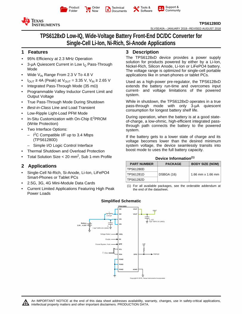
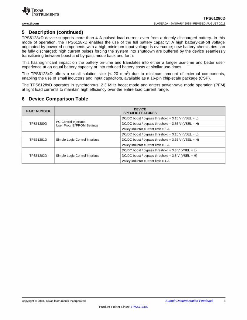
TPS6128xD Low-IQ, Wide-Voltage Battery Front-End DC/DC Converter forSingle-Cell Li-Ion, Ni-Rich, Si-Anode Applications
1
1 Features1• 95% Efficiency at 2.3 MHz Operation• 3-µA Quiescent Current in Low IQ Pass-Through
Mode• Wide VIN Range From 2.3 V To 4.8 V• IOUT ≥ 4A (Peak) at VOUT = 3.35 V, VIN ≥ 2.65 V• Integrated Pass-Through Mode (35 mΩ)• Programmable Valley Inductor Current Limit and
Output Voltage• True Pass-Through Mode During Shutdown• Best-in-Class Line and Load Transient• Low-Ripple Light-Load PFM Mode• In-Situ Customization with On-Chip E2PROM
(Write Protection)• Two Interface Options:
– I2C Compatible I/F up to 3.4 Mbps(TPS61280D)
– Simple I/O Logic Control Interface• Thermal Shutdown and Overload Protection• Total Solution Size < 20 mm2, Sub 1-mm Profile
2 Applications• Single-Cell Ni-Rich, Si-Anode, Li-Ion, LiFePO4
Smart-Phones or Tablet PCs• 2.5G, 3G, 4G Mini-Module Data Cards• Current Limited Applications Featuring High Peak
Power Loads
3 DescriptionThe TPS6128xD device provides a power supplysolution for products powered by either by a Li-Ion,Nickel-Rich, Silicon Anode, Li-Ion or LiFePO4 battery.The voltage range is optimized for single-cell portableapplications like in smart-phones or tablet PCs.
Used as a high-power pre-regulator, the TPS6128xDextends the battery run-time and overcomes inputcurrent- and voltage limitations of the poweredsystem.
While in shutdown, the TPS6128xD operates in a truepass-through mode with only 3-µA quiescentconsumption for longest battery shelf life.
During operation, when the battery is at a good state-of-charge, a low-ohmic, high-efficient integrated pass-through path connects the battery to the poweredsystem.
If the battery gets to a lower state of charge and itsvoltage becomes lower than the desired minimumsystem voltage, the device seamlessly transits intoboost mode to uses the full battery capacity.
Device Information(1)
PART NUMBER PACKAGE BODY SIZE (NOM)TPS61280D
DSBGA (16) 1.66 mm x 1.66 mmTPS61281DTPS61282D
(1) For all available packages, see the orderable addendum atthe end of the datasheet.
Simplified Schematic
2
TPS61280DSLVSEA0A –JANUARY 2018–REVISED AUGUST 2018 www.ti.com
Product Folder Links: TPS61280D
Submit Documentation Feedback Copyright © 2018, Texas Instruments Incorporated
Table of Contents1 Features .................................................................. 12 Applications ........................................................... 13 Description ............................................................. 14 Revision History..................................................... 25 Description (continued)......................................... 36 Device Comparison Table ..................................... 37 Pin Configuration and Functions ......................... 48 Specifications......................................................... 6
8.1 Absolute Maximum Ratings ..................................... 68.2 ESD Ratings.............................................................. 68.3 Recommended Operating Conditions....................... 68.4 Thermal Information .................................................. 78.5 Electrical Characteristics........................................... 78.6 I2C Interface Timing Characteristics ........................ 98.7 I2C Timing Diagrams............................................... 118.8 Typical Characteristics ............................................ 12
9 Detailed Description ............................................ 149.1 Overview ................................................................. 149.2 Functional Block Diagram ....................................... 159.3 Feature Description................................................. 16
9.4 Device Functional Modes........................................ 179.5 Programming........................................................... 229.6 Register Maps ......................................................... 25
10 Application and Implementation........................ 3310.1 Application Information.......................................... 3310.2 Typical Application ................................................ 34
11 Power Supply Recommendations ..................... 4612 Layout................................................................... 46
12.1 Layout Guidelines ................................................. 4612.2 Layout Example .................................................... 4612.3 Thermal Information .............................................. 47
13 Device and Documentation Support ................. 4813.1 Device Support...................................................... 4813.2 Receiving Notification of Documentation Updates 4813.3 Community Resources.......................................... 4813.4 Trademarks ........................................................... 4813.5 Electrostatic Discharge Caution............................ 4813.6 Glossary ................................................................ 48
14 Mechanical, Packaging, and OrderableInformation ........................................................... 4914.1 Package Summary................................................ 49
4 Revision History
Changes from Original (January 2018) to Revision A Page
• Changed devices TPS61281D and TPS61282D From: Product Preview To: Production data ............................................. 1• Changed the TPS61280D pin configuration........................................................................................................................... 4• Changed the TPS6128xD pin configuration ........................................................................................................................... 5
3
TPS61280Dwww.ti.com SLVSEA0A –JANUARY 2018–REVISED AUGUST 2018
Product Folder Links: TPS61280D
Submit Documentation FeedbackCopyright © 2018, Texas Instruments Incorporated
5 Description (continued)TPS6128xD device supports more than 4 A pulsed load current even from a deeply discharged battery. In thismode of operation, the TPS6128xD enables the use of the full battery capacity: A high battery-cut-off voltageoriginated by powered components with a high minimum input voltage is overcome; new battery chemistries canbe fully discharged; high current pulses forcing the system into shutdown are buffered by the device seamlesslytransitioning between boost and by-pass mode back and forth.
This has significant impact on the battery on-time and translates into either a longer use-time and better user-experience at an equal battery capacity or into reduced battery costs at similar use-times.
The TPS6128xD offers a small solution size (< 20 mm2) due to minimum amount of external components,enabling the use of small inductors and input capacitors, available as a 16-pin chip-scale package (CSP).
The TPS6128xD operates in synchronous, 2.3 MHz boost mode and enters power-save mode operation (PFM)at light load currents to maintain high efficiency over the entire load current range.
6 Device Comparison Table
PART NUMBER DEVICESPECIFIC FEATURES
TPS61280D I2C Control InterfaceUser Prog. E2PROM Settings
DC/DC boost / bypass threshold = 3.15 V (VSEL = L)DC/DC boost / bypass threshold = 3.35 V (VSEL = H)Valley inductor current limit = 3 A
TPS61281D Simple Logic Control InterfaceDC/DC boost / bypass threshold = 3.15 V (VSEL = L)DC/DC boost / bypass threshold = 3.35 V (VSEL = H)Valley inductor current limit = 3 A
TPS61282D Simple Logic Control InterfaceDC/DC boost / bypass threshold = 3.3 V (VSEL = L)DC/DC boost / bypass threshold = 3.5 V (VSEL = H)Valley inductor current limit = 4 A
1 2 3 4
D
C
B
A
Not to scale
AGND PGND PGND PGND
nBYP SDA SW SW
VSEL SCL VOUT VOUT
EN GPIO VIN VIN
1 2 3 4
A
B
C
D
Not to scale
EN GPIO VIN VIN
VSEL SCL VOUT VOUT
nBYP SDA SW SW
AGND PGND PGND PGND
4
TPS61280DSLVSEA0A –JANUARY 2018–REVISED AUGUST 2018 www.ti.com
Product Folder Links: TPS61280D
Submit Documentation Feedback Copyright © 2018, Texas Instruments Incorporated
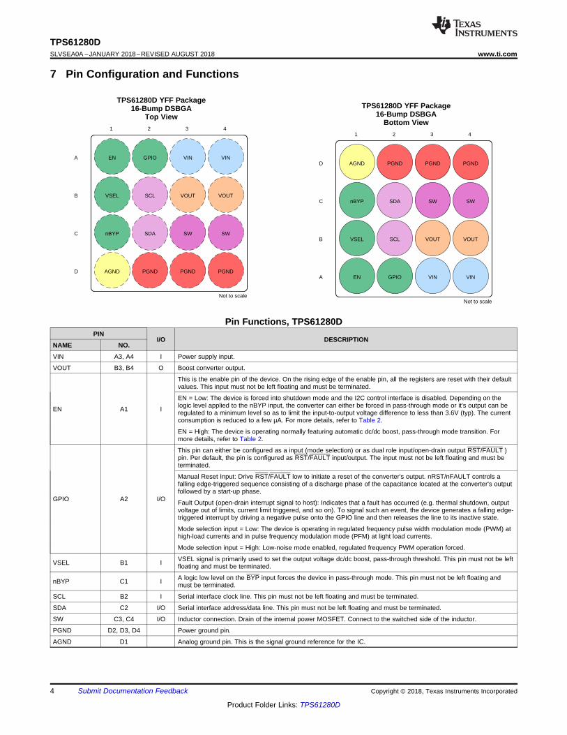
7 Pin Configuration and Functions
TPS61280D YFF Package16-Bump DSBGA
Top ViewTPS61280D YFF Package
16-Bump DSBGABottom View
Pin Functions, TPS61280DPIN
I/O DESCRIPTIONNAME NO.
VIN A3, A4 I Power supply input.
VOUT B3, B4 O Boost converter output.
EN A1 I
This is the enable pin of the device. On the rising edge of the enable pin, all the registers are reset with their defaultvalues. This input must not be left floating and must be terminated.
EN = Low: The device is forced into shutdown mode and the I2C control interface is disabled. Depending on thelogic level applied to the nBYP input, the converter can either be forced in pass-through mode or it's output can beregulated to a minimum level so as to limit the input-to-output voltage difference to less than 3.6V (typ). The currentconsumption is reduced to a few µA. For more details, refer to Table 2.
EN = High: The device is operating normally featuring automatic dc/dc boost, pass-through mode transition. Formore details, refer to Table 2.
GPIO A2 I/O
This pin can either be configured as a input (mode selection) or as dual role input/open-drain output RST/FAULT )pin. Per default, the pin is configured as RST/FAULT input/output. The input must not be left floating and must beterminated.
Manual Reset Input: Drive RST/FAULT low to initiate a reset of the converter's output. nRST/nFAULT controls afalling edge-triggered sequence consisting of a discharge phase of the capacitance located at the converter's outputfollowed by a start-up phase.
Fault Output (open-drain interrupt signal to host): Indicates that a fault has occurred (e.g. thermal shutdown, outputvoltage out of limits, current limit triggered, and so on). To signal such an event, the device generates a falling edge-triggered interrupt by driving a negative pulse onto the GPIO line and then releases the line to its inactive state.
Mode selection input = Low: The device is operating in regulated frequency pulse width modulation mode (PWM) athigh-load currents and in pulse frequency modulation mode (PFM) at light load currents.
Mode selection input = High: Low-noise mode enabled, regulated frequency PWM operation forced.
VSEL B1 I VSEL signal is primarily used to set the output voltage dc/dc boost, pass-through threshold. This pin must not be leftfloating and must be terminated.
nBYP C1 I A logic low level on the BYP input forces the device in pass-through mode. This pin must not be left floating andmust be terminated.
SCL B2 I Serial interface clock line. This pin must not be left floating and must be terminated.
SDA C2 I/O Serial interface address/data line. This pin must not be left floating and must be terminated.
SW C3, C4 I/O Inductor connection. Drain of the internal power MOSFET. Connect to the switched side of the inductor.
PGND D2, D3, D4 Power ground pin.
AGND D1 Analog ground pin. This is the signal ground reference for the IC.
1 2 3 4
D
C
B
A
Not to scale
AGND PGND PGND PGND
nBYP AGND SW SW
VSEL MODE VOUT VOUT
EN PG VIN VIN
1 2 3 4
A
B
C
D
Not to scale
EN PG VIN VIN
VSEL MODE VOUT VOUT
nBYP AGND SW SW
AGND PGND PGND PGND
5
TPS61280Dwww.ti.com SLVSEA0A –JANUARY 2018–REVISED AUGUST 2018
Product Folder Links: TPS61280D
Submit Documentation FeedbackCopyright © 2018, Texas Instruments Incorporated
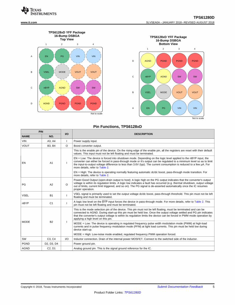
TPS6128xD YFF Package16-Bump DSBGA
Top ViewTPS6128xD YFF Package
16-Bump DSBGABottom View
Pin Functions, TPS6128xDPIN
I/O DESCRIPTIONNAME NO.
VIN A3, A4 I Power supply input.
VOUT B3, B4 O Boost converter output.
EN A1 I
This is the enable pin of the device. On the rising edge of the enable pin, all the registers are reset with their defaultvalues. This input must not be left floating and must be terminated.
EN = Low: The device is forced into shutdown mode. Depending on the logic level applied to the nBYP input, theconverter can either be forced in pass-through mode or it's output can be regulated to a minimum level so as to limitthe input-to-output voltage difference to less than 3.6V (typ). The current consumption is reduced to a few µA. Formore details, refer to Table 2.
EN = High: The device is operating normally featuring automatic dc/dc boost, pass-through mode transition. Formore details, refer to Table 2.
PG A2 O
Power-Good Output (open-drain output to host): A logic high on the PG output indicates that the converter's outputvoltage is within its regulation limits. A logic low indicates a fault has occurred (e.g. thermal shutdown, output voltageout of limits, current limit triggered, and so on). The PG signal is de-asserted automatically once the IC resumesproper operation.
VSEL B1 I VSEL signal is primarily used to set the output voltage dc/dc boost, pass-through threshold. This pin must not be leftfloating and must be terminated.
nBYP C1 I A logic low level on the BYP input forces the device in pass-through mode. For more details, refer to Table 2. Thispin must not be left floating and must be terminated.
MODE B2 I
This is the mode selection pin of the device. This pin must not be left floating, must be terminated and can beconnected to AGND. During start-up this pin must be held low. Once the output voltage settled and PG pin indicatesthat the converter's output voltage is within its regulation limits the device can be forced in PWM mode operation byapplying a high level on this pin.
MODE = Low: The device is operating in regulated frequency pulse width modulation mode (PWM) at high-loadcurrents and in pulse frequency modulation mode (PFM) at light load currents. This pin must be held low duringdevice start-up.
MODE = High: Low-noise mode enabled, regulated frequency PWM operation forced.
SW C3, C4 I/O Inductor connection. Drain of the internal power MOSFET. Connect to the switched side of the inductor.
PGND D2, D3, D4 Power ground pin.
AGND C2, D1 Analog ground pin. This is the signal ground reference for the IC.
6
TPS61280DSLVSEA0A –JANUARY 2018–REVISED AUGUST 2018 www.ti.com
Product Folder Links: TPS61280D
Submit Documentation Feedback Copyright © 2018, Texas Instruments Incorporated
(1) Stresses beyond those listed under absolute maximum ratings may cause permanent damage to the device. These are stress ratingsonly, and functional operation of the device at these or any other conditions beyond those indicated under recommended operatingconditions is not implied. Exposure to absolute-maximum-rated conditions for extended periods my affect device reliability.
(2) All voltages are with respect to network ground terminal.(3) Limit the junction temperature to 105°C for continuous operation at maximum output power.(4) Limit the junction temperature to 105°C for 15% duty cycle operation.(5) In applications where high power dissipation and/or poor package thermal resistance is present, the maximum ambient temperature may
have to be derated. Maximum ambient temperature (TA(max)) is dependent on the maximum operating junction temperature (TJ(max)), themaximum power dissipation of the device in the application (PD(max)), and the junction-to-ambient thermal resistance of the part/packagein the application (θJA), as given by the following equation: TA(max) = TJ(max) – (θJA X PD(max)). To achieve optimum performance, it isrecommended to operate the device with a maximum junction temperature of 105°C.
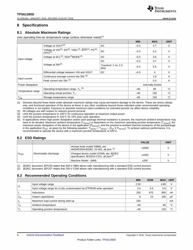
8 Specifications
8.1 Absolute Maximum Ratingsover operating free-air temperature range (unless otherwise noted) (1)
MIN MAX UNIT
Input voltage
Voltage at VOUT (2) DC –0.3 4.7 VVoltage at VIN (2), EN (2), VSEL (2), BYP (2), PG (2),GPIO (2) DC –0.3 5.2 V
Voltage at SCL (2), SDA (2)MODE (2) DC –0.3 3.6 V
Voltage at SW (2)DC –0.3 4.7 VTransient: 2 ns, 2.3MHz –0.3 5.5 V
Differential voltage between VIN and VOUT DC –0.3 4 V
Input currentContinuous average current into SW (3) 1.8 APeak current into SW (4) 5.5 A
Power dissipation Internally limited
Temperature rangeOperating temperature range, TA
(5) –40 85 °COperating virtual junction, TJ –40 150 °C
Tstg Storage temperature range –65 150 °C
(1) JEDEC document JEP155 states that 500-V HBM allows safe manufacturing with a standard ESD control process.(2) JEDEC document JEP157 states that 250-V CDM allows safe manufacturing with a standard ESD control process.
8.2 ESD RatingsVALUE UNIT
VESD Electrostatic discharge
Human body model (HBM), perANSI/ESDA/JEDEC JS-001, all pins (1) ±2000 V
Charged device model (CDM), per JEDECspecification JESD22-C101, all pins (2) ±1000 V
Machine Model - (MM) ±200 V
8.3 Recommended Operating ConditionsMIN NOM MAX UNIT
VIInput voltage range 2.30 4.85 VInput voltage range for in-situ customization by E2PROM write operation 3.4 3.5 3.6 V
L Inductance 200 470 800 nHCO Output capacitance 9 13 100 µFIL Maximum load current during start-up 250 mATA Ambient temperature –40 85 °CTJ Operating junction temperature –40 125 °C
7
TPS61280Dwww.ti.com SLVSEA0A –JANUARY 2018–REVISED AUGUST 2018
Product Folder Links: TPS61280D
Submit Documentation FeedbackCopyright © 2018, Texas Instruments Incorporated
(1) For more information about traditional and new thermal metrics, see the Semiconductor and IC Package Thermal Metrics applicationreport.
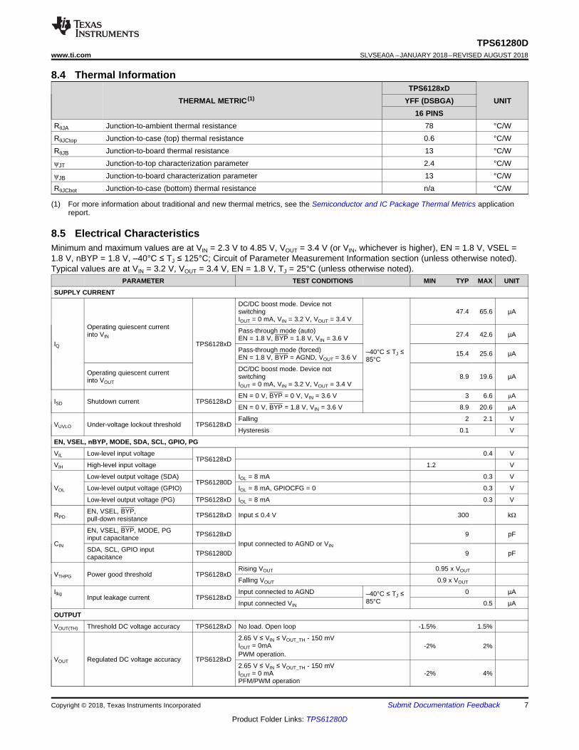
8.4 Thermal Information
THERMAL METRIC (1)TPS6128xD
UNITYFF (DSBGA)16 PINS
RθJA Junction-to-ambient thermal resistance 78 °C/WRθJCtop Junction-to-case (top) thermal resistance 0.6 °C/WRθJB Junction-to-board thermal resistance 13 °C/WψJT Junction-to-top characterization parameter 2.4 °C/WψJB Junction-to-board characterization parameter 13 °C/WRθJCbot Junction-to-case (bottom) thermal resistance n/a °C/W
8.5 Electrical CharacteristicsMinimum and maximum values are at VIN = 2.3 V to 4.85 V, VOUT = 3.4 V (or VIN, whichever is higher), EN = 1.8 V, VSEL =1.8 V, nBYP = 1.8 V, –40°C ≤ TJ ≤ 125°C; Circuit of Parameter Measurement Information section (unless otherwise noted).Typical values are at VIN = 3.2 V, VOUT = 3.4 V, EN = 1.8 V, TJ = 25°C (unless otherwise noted).
PARAMETER TEST CONDITIONS MIN TYP MAX UNIT
SUPPLY CURRENT
IQ
Operating quiescent currentinto VIN
TPS6128xD
DC/DC boost mode. Device notswitchingIOUT = 0 mA, VIN = 3.2 V, VOUT = 3.4 V
–40°C ≤ TJ ≤85°C
47.4 65.6 µA
Pass-through mode (auto)EN = 1.8 V, BYP = 1.8 V, VIN = 3.6 V 27.4 42.6 µA
Pass-through mode (forced)EN = 1.8 V, BYP = AGND, VOUT = 3.6 V 15.4 25.6 µA
Operating quiescent currentinto VOUT
DC/DC boost mode. Device notswitchingIOUT = 0 mA, VIN = 3.2 V, VOUT = 3.4 V
8.9 19.6 µA
ISD Shutdown current TPS6128xDEN = 0 V, BYP = 0 V, VIN = 3.6 V 3 6.6 μA
EN = 0 V, BYP = 1.8 V, VIN = 3.6 V 8.9 20.6 μA
VUVLO Under-voltage lockout threshold TPS6128xDFalling 2 2.1 V
Hysteresis 0.1 V
EN, VSEL, nBYP, MODE, SDA, SCL, GPIO, PG
VIL Low-level input voltageTPS6128xD
0.4 V
VIH High-level input voltage 1.2 V
VOL
Low-level output voltage (SDA)TPS61280D
IOL = 8 mA 0.3 V
Low-level output voltage (GPIO) IOL = 8 mA, GPIOCFG = 0 0.3 V
Low-level output voltage (PG) TPS6128xD IOL = 8 mA 0.3 V
RPDEN, VSEL, BYP,pull-down resistance TPS6128xD Input ≤ 0.4 V 300 kΩ
CIN
EN, VSEL, BYP, MODE, PGinput capacitance TPS6128xD
Input connected to AGND or VIN
9 pF
SDA, SCL, GPIO inputcapacitance TPS61280D 9 pF
VTHPG Power good threshold TPS6128xDRising VOUT 0.95 x VOUT
Falling VOUT 0.9 x VOUT
IlkgInput leakage current TPS6128xD
Input connected to AGND –40°C ≤ TJ ≤85°C
0 µA
Input connected VIN 0.5 µA
OUTPUT
VOUT(TH) Threshold DC voltage accuracy TPS6128xD No load. Open loop -1.5% 1.5%
VOUT Regulated DC voltage accuracy TPS6128xD
2.65 V ≤ VIN ≤ VOUT_TH - 150 mVIOUT = 0mAPWM operation.
-2% 2%
2.65 V ≤ VIN ≤ VOUT_TH - 150 mVIOUT = 0 mAPFM/PWM operation
-2% 4%

8
TPS61280DSLVSEA0A –JANUARY 2018–REVISED AUGUST 2018 www.ti.com
Product Folder Links: TPS61280D
Submit Documentation Feedback Copyright © 2018, Texas Instruments Incorporated
Electrical Characteristics (continued)Minimum and maximum values are at VIN = 2.3 V to 4.85 V, VOUT = 3.4 V (or VIN, whichever is higher), EN = 1.8 V, VSEL =1.8 V, nBYP = 1.8 V, –40°C ≤ TJ ≤ 125°C; Circuit of Parameter Measurement Information section (unless otherwise noted).Typical values are at VIN = 3.2 V, VOUT = 3.4 V, EN = 1.8 V, TJ = 25°C (unless otherwise noted).
PARAMETER TEST CONDITIONS MIN TYP MAX UNIT
(1) Specified by characterization. Not tested in production.
ΔVOUT
Power-save modeoutput ripple voltage TPS6128xD
PFM operation, IOUT = 1 mA 30 mVpk
PWM mode output ripple voltage PWM operation, IOUT = 500 mA 15 mVpk
POWER SWITCH
rDS(on)
Low-side switch MOSFETon resistance
TPS6128xD
VIN = 3.2 V, VOUT = 3.5 V 45 80 mΩ
High-side rectifier MOSFETon resistance VIN = 3.2 V, VOUT = 3.5 V 40 70 mΩ
High-side pass-through MOSFETon resistance VIN = 3.2 V 35 60 mΩ
Ilkg
Reverse leakage current into SW
TPS6128xD
EN = AGND, VIN = VOUT = SW = 3.5 V–40°C ≤ TJ ≤ 85°C 0.1 2 µA
Reverse leakage current intoVOUT
EN = BYP = VIN, VIN = 2.9 V, VOUT = 4.4 V, VSW = 0 Vdevice not switching–40°C ≤ TJ ≤ 85°C
0.11 2 µA
ISINK VOUT sink capability TPS6128xD EN = AGND, VOUT ≤ 3.6 V,IOUT = -10 mA 0.3 V
Valley inductor current limit TPS61280DTPS61281D
VIN = 2.9 V, VOUT = 3.5 V, –40°C ≤ TJ ≤ 125°C, autoPFM/PWM 2475 3000 3525 mA
Valley inductor current limit TPS61282D VIN = 2.9 V, VOUT = 3.5 V, –40°C ≤ TJ ≤ 125°C, autoPFM/PWM 3300 4000 4700 mA
Pass through mode current limit TPS6128xDEN = BYP = GND, VIN = 3.2 V 5000 mA
EN = VIN, BYP = don't care , VIN = 3.2 V 5600 7400 9100 mA
Pre-charge mode current limit(linear mode, phase 1)
TPS6128xD VIN - VOUT >= 300 mV500 650 mA
Pre-charge mode current limit(linear mode, phase 2) 2000 mA
OSCILLATOR
fOSC Oscillator frequency TPS6128xD VIN = 2.7 V, VOUT = 3.5 V 2.3 MHz
THERMAL SHUTDOWN, HOT DIE DETECTOR
Thermal shutdown (1) TPS6128xD 140 160 °C
Hot die detector accuracy (1) TPS61280D -10 105 10 °C
TIMING
Start-up time TPS6128xD VIN = 3.2 V, VOUT_TH = 01011 (3.4 V), RLOAD = 50 ΩTime from active VIN to VOUT settled 500 µs
GPIO rise time (1) TPS61280D 200 ns
9
TPS61280Dwww.ti.com SLVSEA0A –JANUARY 2018–REVISED AUGUST 2018
Product Folder Links: TPS61280D
Submit Documentation FeedbackCopyright © 2018, Texas Instruments Incorporated
(1) Specified by design. Not tested in production.
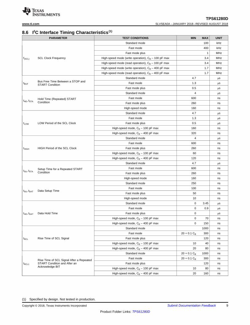
8.6 I2C Interface Timing Characteristics (1)
PARAMETER TEST CONDITIONS MIN MAX UNIT
f(SCL) SCL Clock Frequency
Standard mode 100 kHz
Fast mode 400 kHz
Fast mode plus 1 MHz
High-speed mode (write operation), CB – 100 pF max 3.4 MHz
High-speed mode (read operation), CB – 100 pF max 3.4 MHz
High-speed mode (write operation), CB – 400 pF max 1.7 MHz
High-speed mode (read operation), CB – 400 pF max 1.7 MHz
tBUFBus Free Time Between a STOP andSTART Condition
Standard mode 4.7 μs
Fast mode 1.3 μs
Fast mode plus 0.5 μs
tHD, tSTAHold Time (Repeated) STARTCondition
Standard mode 4 μs
Fast mode 600 ns
Fast mode plus 260 ns
High-speed mode 160 ns
tLOW LOW Period of the SCL Clock
Standard mode 4.7 μs
Fast mode 1.3 μs
Fast mode plus 0.5 μs
High-speed mode, CB – 100 pF max 160 ns
High-speed mode, CB – 400 pF max 320 ns
tHIGH HIGH Period of the SCL Clock
Standard mode 4 μs
Fast mode 600 ns
Fast mode plus 260 ns
High-speed mode, CB – 100 pF max 60 ns
High-speed mode, CB – 400 pF max 120 ns
tSU, tSTASetup Time for a Repeated STARTCondition
Standard mode 4.7 μs
Fast mode 600 ns
Fast mode plus 260 ns
High-speed mode 160 ns
tSU, tDAT Data Setup Time
Standard mode 250 ns
Fast mode 100 ns
Fast mode plus 50 ns
High-speed mode 10 ns
tHD, tDAT Data Hold Time
Standard mode 0 3.45 μs
Fast mode 0 0.9 μs
Fast mode plus 0 μs
High-speed mode, CB – 100 pF max 0 70 ns
High-speed mode, CB – 400 pF max 0 150 ns
tRCL Rise Time of SCL Signal
Standard mode 1000 ns
Fast mode 20 + 0.1 CB 300 ns
Fast mode plus 120 ns
High-speed mode, CB – 100 pF max 10 40 ns
High-speed mode, CB – 400 pF max 20 80 ns
tRCL1
Rise Time of SCL Signal After a RepeatedSTART Condition and After anAcknowledge BIT
Standard mode 20 + 0.1 CB 1000 ns
Fast mode 20 + 0.1 CB 300 ns
Fast mode plus 120 ns
High-speed mode, CB – 100 pF max 10 80 ns
High-speed mode, CB – 400 pF max 20 160 ns

10
TPS61280DSLVSEA0A –JANUARY 2018–REVISED AUGUST 2018 www.ti.com
Product Folder Links: TPS61280D
Submit Documentation Feedback Copyright © 2018, Texas Instruments Incorporated
I2C Interface Timing Characteristics(1) (continued)PARAMETER TEST CONDITIONS MIN MAX UNIT
tFCL Fall Time of SCL Signal
Standard mode 20 + 0.1 CB 300 ns
Fast mode 300 ns
Fast mode plus 120 ns
High-speed mode, CB – 100 pF max 10 40 ns
High-speed mode, CB – 400 pF max 20 80 ns
tRDA Rise Time of SDA Signal
Standard mode 1000 ns
Fast mode 20 + 0.1 CB 300 ns
Fast mode plus 120 ns
High-speed mode, CB – 100 pF max 10 80 ns
High-speed mode, CB – 400 pF max 20 160 ns
tFDA Fall Time of SDA Signal
Standard mode 300 ns
Fast mode 20 + 0.1 CB 300 ns
Fast mode plus 120 ns
High-speed mode, CB – 100 pF max 10 80 ns
High-speed mode, CB – 400 pF max 20 160 ns
tSU, tSTO Setup Time of STOP Condition
Standard mode 4 μs
Fast mode 600 ns
Fast mode plus 260 ns
High-Speed mode 160 ns
CB Capacitive Load for SDA and SCL
Standard mode 400 pF
Fast mode 400 pF
Fast mode plus 550 pF
High-Speed mode 400 pF
Sr PSrtfDA trDA
thd;DATtsu;STA thd;STA tsu;DAT
tsu;STO
trCL1tfCL
tHIGH tLOW tLOW tHIGH
trCLtrCL1
= MCS Current Source Pull-Up
= R(P) Resistor Pull-Up
SDAH
SCLH
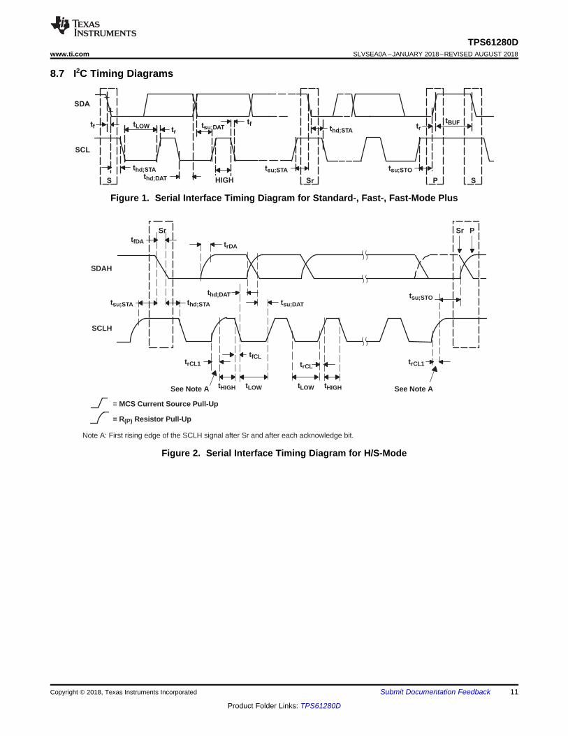
Note A: First rising edge of the SCLH signal after Sr and after each acknowledge bit.
See Note ASee Note A
tf tLOWtr
thd;STA
thd;DAT
tsu;DATtf
HIGH
tsu;STA
S Sr P S
thd;STAtr
tBUF
tsu;STO
SDA
SCL
11
TPS61280Dwww.ti.com SLVSEA0A –JANUARY 2018–REVISED AUGUST 2018
Product Folder Links: TPS61280D
Submit Documentation FeedbackCopyright © 2018, Texas Instruments Incorporated
8.7 I2C Timing Diagrams
Figure 1. Serial Interface Timing Diagram for Standard-, Fast-, Fast-Mode Plus
Figure 2. Serial Interface Timing Diagram for H/S-Mode
10
12
14
16
18
20
3.5 4.5
Qui
esce
nt C
urre
nt_F
orce
Byp
ass
(µA
)
Input Voltage (V)
Tj=25C
Tj=-40
Tj = 85 C
C005
TJ = 30°C
TJ = -40°C
TJ = 85°C 15
17
19
21
23
25
27
29
31
33
35
3.5 4.5
Qui
esce
nt C
urre
nt_A
uto
Byp
ass
(µA
)
Input Voltage (V)
Tj=25C
Tj=-40
Tj = 85 C
C006
TJ = 30°C
TJ = -40°C
TJ = 85°C
30
32
34
36
38
40
42
44
46
48
50
-40 -20 0 20 40 60 80 100 120
LS F
ET
On
Res
ista
nce
(m
Junction Temperature (C) C003
30
40
50
60
2.3 2.5 2.7 2.9 3.1
Qui
esce
nt C
urre
nt_B
oost
(µ
A)
Input Voltage (V)
Tj=25C
Tj=-40
Tj = 85 C
C004
TJ = 30°C
TJ = -40°C
TJ = 85°C
30
32
34
36
38
40
42
44
46
48
50
-40 -20 0 20 40 60 80 100 120
HS
FE
T O
n R
esis
tanc
e (m
Junction Temperature (C) C001
30
35
40
45
50
55
60
65
70
-40 -20 0 20 40 60 80 100 120
LS F
ET
On
Res
ista
nce
(m
Junction Temperature (C) C002
12
TPS61280DSLVSEA0A –JANUARY 2018–REVISED AUGUST 2018 www.ti.com
Product Folder Links: TPS61280D
Submit Documentation Feedback Copyright © 2018, Texas Instruments Incorporated
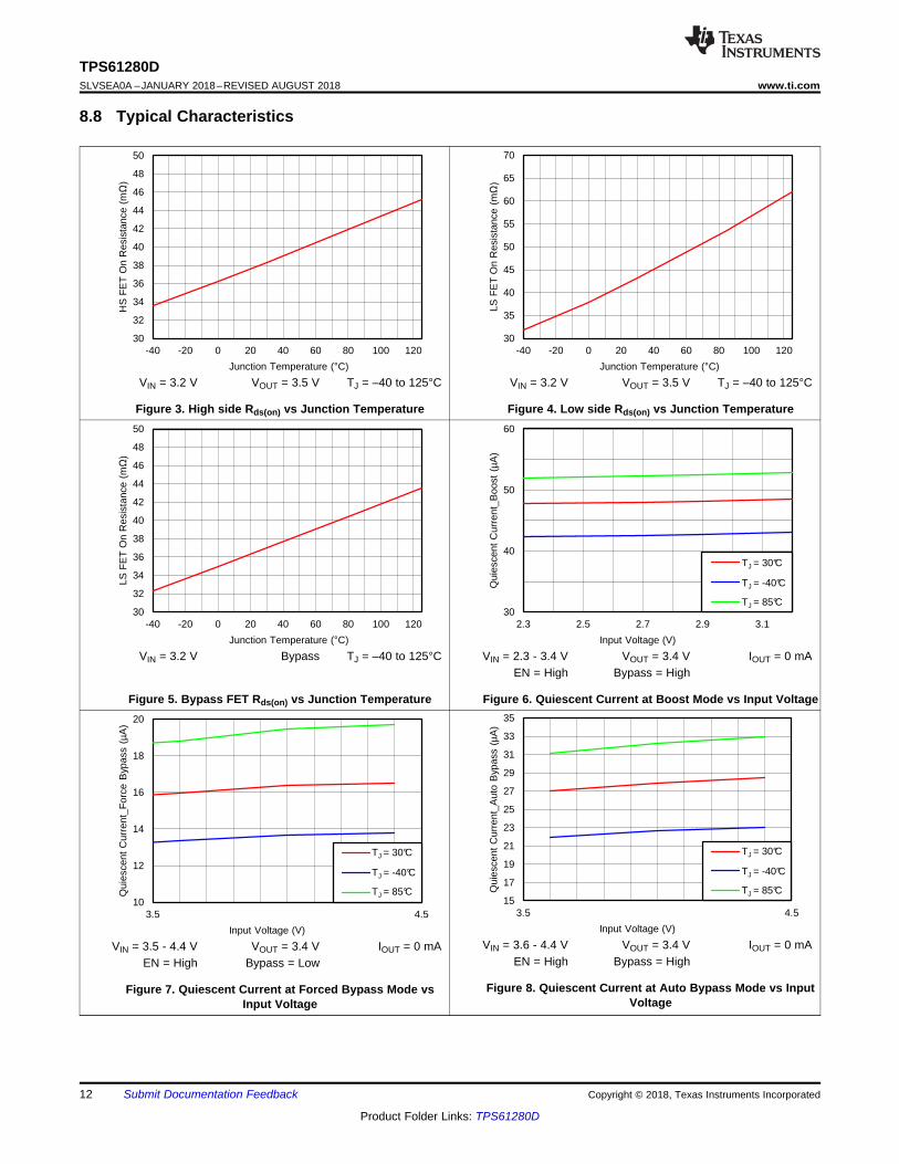
8.8 Typical Characteristics
VIN = 3.2 V VOUT = 3.5 V TJ = –40 to 125°C
Figure 3. High side Rds(on) vs Junction Temperature
VIN = 3.2 V VOUT = 3.5 V TJ = –40 to 125°C
Figure 4. Low side Rds(on) vs Junction Temperature
VIN = 3.2 V Bypass TJ = –40 to 125°C
Figure 5. Bypass FET Rds(on) vs Junction Temperature
VIN = 2.3 - 3.4 V VOUT = 3.4 V IOUT = 0 mAEN = High Bypass = High
Figure 6. Quiescent Current at Boost Mode vs Input Voltage
VIN = 3.5 - 4.4 V VOUT = 3.4 V IOUT = 0 mAEN = High Bypass = Low
Figure 7. Quiescent Current at Forced Bypass Mode vsInput Voltage
VIN = 3.6 - 4.4 V VOUT = 3.4 V IOUT = 0 mAEN = High Bypass = High
Figure 8. Quiescent Current at Auto Bypass Mode vs InputVoltage
0.50
0.60
0.70
0.80
0.90
1.00
1.10
-40 -20 0 20 40 60 80 100 120
EN
Log
ic T
hres
hold
(V
)
Junction Temperature (C)
EN Rising
EN Falling
C011
0.50
0.60
0.70
0.80
0.90
1.00
1.10
-40 -20 0 20 40 60 80 100 120
EN
Log
ic T
hres
hold
(V
)
Junction Temperature (C)
nBYP Rising
nBYP Falling
C012
1.80
2.00
2.20
-40 -20 0 20 40 60 80 100 120
Vin
UV
LO T
hres
hold
(V
)
Junction Temperature (C)
Vin Rising
Vin Falling
C010
VIN Rising
VIN Falling 2.0
2.5
3.0
3.5
4.0
4.5
-40 10 60 110
Sw
itch
Valle
yC
urr
ent
Lim
it (
A)
Temperature ( C)O
TPS61281D
TPS61282D
C009
0
1
2
3
4
5
2.3 3.3 4.3
Leak
age
Cur
rent
_Low
Iq
(µA
)
Input Voltage (V)
Tj=25C
Tj=-40
Tj = 85 C
C007
TJ = 30°C
TJ = -40°C
TJ = 85°C 3
4
5
6
7
8
9
10
11
12
13
2.3 3.3 4.3
Leak
age
Cur
rent
_Low
Iq
(µA
)
Input Voltage (V)
Tj = 25C
Tj = -40
Tj = 85 C
C008
TJ = 30°C
TJ = -40°C
TJ = 85°C
13
TPS61280Dwww.ti.com SLVSEA0A –JANUARY 2018–REVISED AUGUST 2018
Product Folder Links: TPS61280D
Submit Documentation FeedbackCopyright © 2018, Texas Instruments Incorporated
Typical Characteristics (continued)
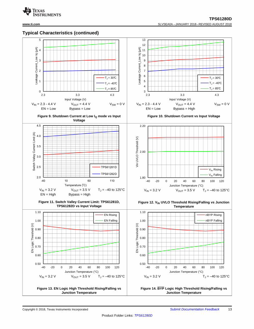
VIN = 2.3 - 4.4 V VOUT = 4.4 V VSW = 0 VEN = Low Bypass = Low
Figure 9. Shutdown Current at Low IQ mode vs InputVoltage
VIN = 2.3 - 4.4 V VOUT = 4.4 V VSW = 0 VEN = Low Bypass = High
Figure 10. Shutdown Current vs Input Voltage
VIN = 3.2 V VOUT = 3.5 V TJ = –40 to 125°CEN = High Bypass = High
Figure 11. Switch Valley Current Limit: TPS61281D,TPS61282D vs Input Voltage
VIN = 3.2 V VOUT = 3.5 V TJ = –40 to 125°C
Figure 12. VIN UVLO Threshold Rising/Falling vs JunctionTemperature
VIN = 3.2 V VOUT = 3.5 V TJ = –40 to 125°C
Figure 13. EN Logic High Threshold Rising/Falling vsJunction Temperature
VIN = 3.2 V TJ = –40 to 125°C
Figure 14. BYP Logic High Threshold Rising/Falling vsJunction Temperature
14
TPS61280DSLVSEA0A –JANUARY 2018–REVISED AUGUST 2018 www.ti.com
Product Folder Links: TPS61280D
Submit Documentation Feedback Copyright © 2018, Texas Instruments Incorporated
9 Detailed Description
9.1 OverviewThe TPS6128xD is a high-efficiency step-up converter featuring pass-through mode optimized to provide low-noise voltage supply for 2G RF power amplifiers (PAs) in mobile phones and/or to pre-regulate voltage forsupplying subsystem like eMMC memory, audio codec, LCD bias, antenna switches, RF engine PMIC and so on.It is designed to allow the system to operate at maximum efficiency for a wide range of power consumption levelsfrom a low-, wide- voltage battery cell.
The capability of the TPS6128xD to step-up the voltage as well as to pass-through the input battery voltagewhen its level is high enough allow systems to operate at maximum performance over a wide range of batteryvoltages, thereby extending the battery life between charging. The device also addresses brownouts caused bythe peak currents drawn by the APU and GPU which can cause the battery rail to droop momentarily. Using theTPS6128xD device as a pre-regulator eliminates system brownout condition while maintaining a stable supplyrail for critical sub-system to function properly.
The TPS6128xD synchronous step-up converter typically operates at a quasi-constant 2.3-MHz frequency pulsewidth modulation (PWM) at moderate to heavy load currents. At light load currents, the TPS6128xD converteroperates in power-save mode with pulse frequency modulation (PFM).
In general, a dc/dc step-up converter can only operate in "true" boost mode, that is the output “boosted” by acertain amount above the input voltage. The TPS6128xD device operates differently as it can smoothly transitionin and out of zero duty cycle operation. Depending upon the input voltage, output voltage threshold and loadcurrent, the integrated bypass switch automatically transitions the converter into pass-through mode to maintainlow-dropout and high-efficiency. The device exits pass-through mode (0% duty cycle operation) if the totaldropout resistance in bypass mode is insufficient to maintain the output voltage at it's nominal level. Refer to thetypical characteristics section (DC Output Voltage vs. Input Voltage) for further details.
During PWM operation, the converter uses a novel quasi-constant on-time valley current mode control scheme toachieve excellent line/load regulation and allows the use of a small ceramic inductor and capacitors. Based onthe VIN/VOUT ratio, a simple circuit predicts the required on-time. At the beginning of the switching cycle, the low-side N-MOS switch is turned-on and the inductor current ramps up to a peak current that is defined by the on-time and the inductance. In the second phase, once the on-timer has expired, the rectifier is turned-on and theinductor current decays to a preset valley current threshold. Finally, the switching cycle repeats by setting the ontimer again and activating the low-side N-MOS switch.
The current mode architecture provides excellent transient load response, requiring minimal output filtering.Internal soft-start and loop compensation simplifies the design process while minimizing the number of externalcomponents.
The TPS6128xD directly and accurately controls the average input current through intelligent adjustment of thevalley current limit, allowing an accuracy of ±17.5%. Together with an external bulk capacitor, the TPS6128xDallows an application to be interfaced directly to its load, without overloading the input source due to appropriateset average input current limit. An open-drain output (PG or GPIO/nFAULT) provides a signal to issue aninterrupt to the system if any fault is detected on the device (thermal shutdown, output voltage out-of limits, andso on).
The output voltage can be dynamically adjusted between two values (floor and roof voltages) by toggling a logiccontrol input (VSEL) without the need for external feedback resistors. This features can either be used to raisethe output voltage in anticipation of a positive load transient or to dynamically change the PA supply voltagedepending on its mode of operation and/or transmitting power.
The TPS61280D integrates an I2C compatible interface allowing transfers up to 3.4Mbps. This communicationinterface can be used to set the output voltage threshold at which the converter transitions between boost andpass-through mode, for reprogramming the mode of operation (PFM/PWM or forced PWM), for settings theaverage input current limit or resetting the output voltage for instance.
Configuration parameters can be changed by writing the desired values to the appropriate I2C register(s). TheI2C registers are volatile and their contents are lost when power is removed from the device. By writing to theE2PROMCTRL Register [reset = 0xFF], it is possible to store the active configuration in non-volatile E2PROM;during power-up, the contents of the E2PROM are copied into the I2C registers and used to configure the device.
15
TPS61280Dwww.ti.com SLVSEA0A –JANUARY 2018–REVISED AUGUST 2018
Product Folder Links: TPS61280D
Submit Documentation FeedbackCopyright © 2018, Texas Instruments Incorporated
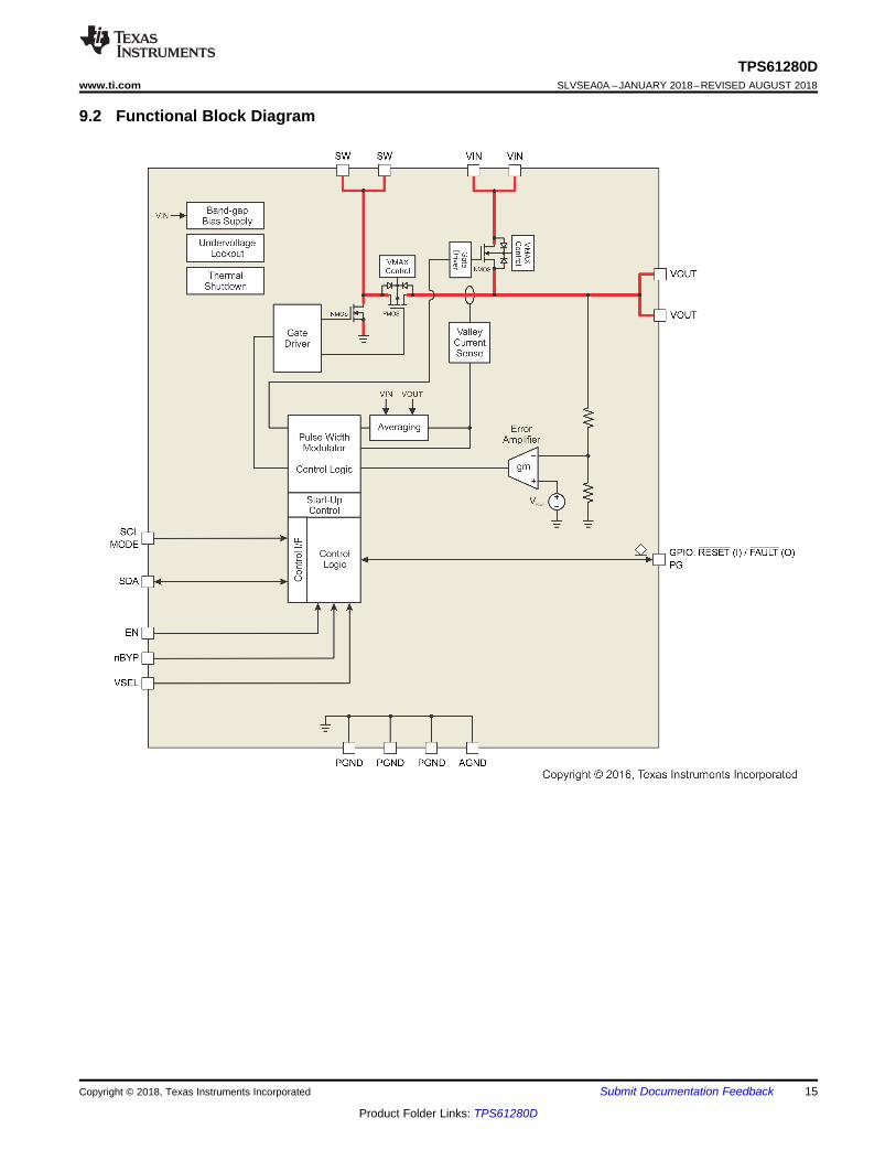
9.2 Functional Block Diagram
( )( )hmfB
ffmfB
fmh
mcfm
×+××=
+D×=+××=
12
)(212
( ) )(212mcfm
ffmfB +D×=+××=
0 dBV
0 dBVref
F1
FENV,PEAK Dfc Dfc Non-modulated harmonic
Side-band harmonics
window after modulation
16
TPS61280DSLVSEA0A –JANUARY 2018–REVISED AUGUST 2018 www.ti.com
Product Folder Links: TPS61280D
Submit Documentation Feedback Copyright © 2018, Texas Instruments Incorporated
9.3 Feature Description
9.3.1 Voltage Scaling Management (VSEL)In order to maintain a certain minimum output voltage under heavy load transients, the output voltage set pointcan be dynamically increased by asserting the VSEL input. The functionality also helps to mitigate undershootduring severe line transients, while minimizing the output voltage during more benign operating conditions tosave power.
The output voltage ramps up (floor to roof transition) at pre-defined rate defined by the average input current limitsetting. The required time to ramp down the voltage (roof to floor transition) largely depends on the amount ofcapacitance present at the converter's output as well as on the load current. Table 1 shows the ramp rate controlwhen transitioning to a lower voltage.
Table 1. Ramp Down Rate vs. Target ModeMode Associated with Floor Voltage Output Voltage Ramp Rate
Forced PWM Output capacitance is being discharged at a rate of approx. 50mA (or higher) constant currentin addition to the load current drawn
PFM Output capacitance is being discharged (solely) by the load current drawn
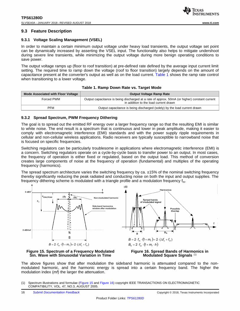
(1) Spectrum illustrations and formulae (Figure 15 and Figure 16) copyright IEEE TRANSACTIONS ON ELECTROMAGNETICCOMPATIBILITY, VOL. 47, NO.3, AUGUST 2005.
9.3.2 Spread Spectrum, PWM Frequency DitheringThe goal is to spread out the emitted RF energy over a larger frequency range so that the resulting EMI is similarto white noise. The end result is a spectrum that is continuous and lower in peak amplitude, making it easier tocomply with electromagnetic interference (EMI) standards and with the power supply ripple requirements incellular and non-cellular wireless applications. Radio receivers are typically susceptible to narrowband noise thatis focused on specific frequencies.
Switching regulators can be particularly troublesome in applications where electromagnetic interference (EMI) isa concern. Switching regulators operate on a cycle-by-cycle basis to transfer power to an output. In most cases,the frequency of operation is either fixed or regulated, based on the output load. This method of conversioncreates large components of noise at the frequency of operation (fundamental) and multiples of the operatingfrequency (harmonics).
The spread spectrum architecture varies the switching frequency by ca. ±15% of the nominal switching frequencythereby significantly reducing the peak radiated and conducting noise on both the input and output supplies. Thefrequency dithering scheme is modulated with a triangle profile and a modulation frequency fm.
Figure 15. Spectrum of a Frequency ModulatedSin. Wave with Sinusoidal Variation in Time
Figure 16. Spread Bands of Harmonics inModulated Square Signals (1)
The above figures show that after modulation the sideband harmonic is attenuated compared to the non-modulated harmonic, and the harmonic energy is spread into a certain frequency band. The higher themodulation index (mf) the larger the attenuation.
( ) ( )m c mB = 2 1 + m = 2 +¦´ ¦ ´ ´ D¦ ¦
c
c
ƒ=
ƒ
Dd
cƒ
m
δ ƒm =
ƒ
´
17
TPS61280Dwww.ti.com SLVSEA0A –JANUARY 2018–REVISED AUGUST 2018
Product Folder Links: TPS61280D
Submit Documentation FeedbackCopyright © 2018, Texas Instruments Incorporated
where• fc is the carrier frequency (approx. 2.3MHz)• fm is the modulating frequency (approx. 40kHz)• δ is the modulation ratio (approx 0.15) (1)
(2)
The maximum switching frequency fc is limited by the process and finally the parameter modulation ratio (δ),together with fm , which is the side-band harmonics bandwidth around the carrier frequency fc. The bandwidth ofa frequency modulated waveform is approximately given by the Carson’s rule and can be summarized as:
(3)
fm < RBW: The receiver is not able to distinguish individual side-band harmonics, so, several harmonics areadded in the input filter and the measured value is higher than expected in theoretical calculations.
fm > RBW: The receiver is able to properly measure each individual side-band harmonic separately, so themeasurements match with the theoretical calculations.
9.4 Device Functional Modes
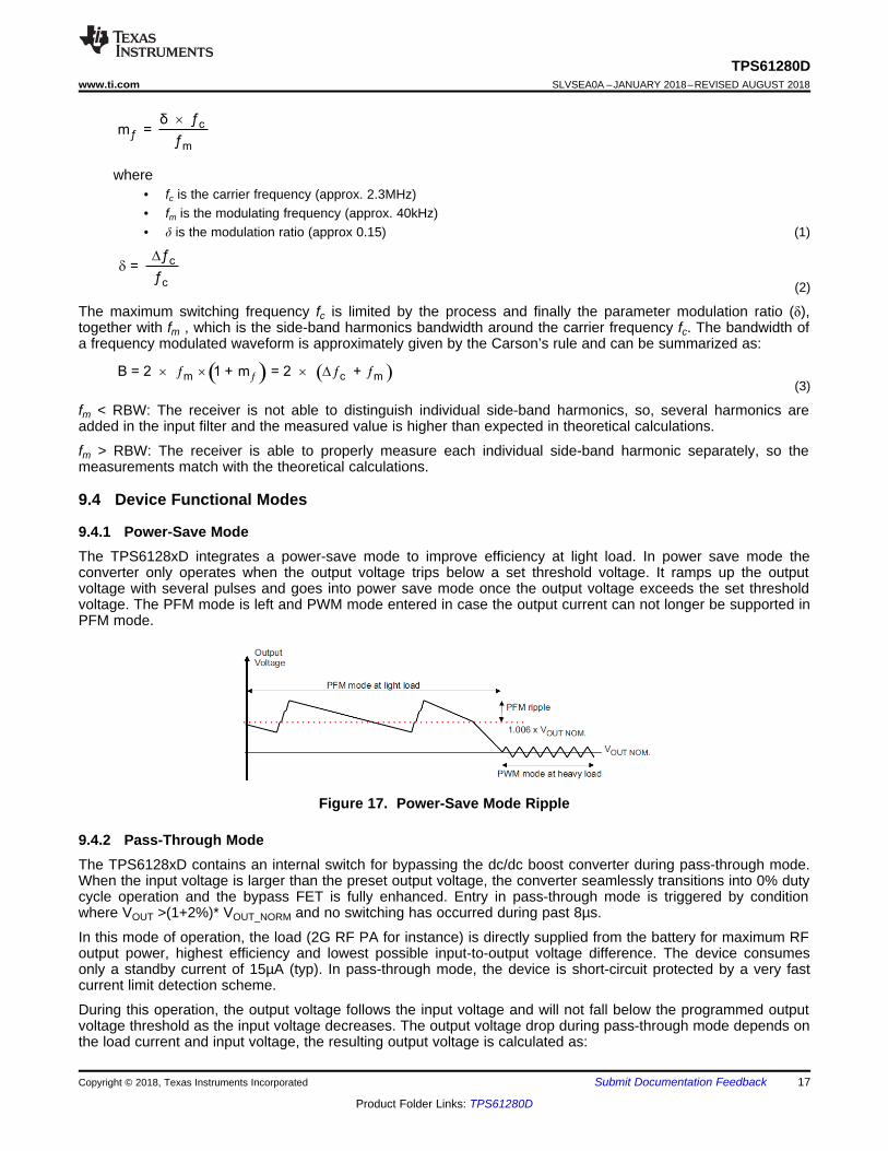
9.4.1 Power-Save ModeThe TPS6128xD integrates a power-save mode to improve efficiency at light load. In power save mode theconverter only operates when the output voltage trips below a set threshold voltage. It ramps up the outputvoltage with several pulses and goes into power save mode once the output voltage exceeds the set thresholdvoltage. The PFM mode is left and PWM mode entered in case the output current can not longer be supported inPFM mode.
Figure 17. Power-Save Mode Ripple
9.4.2 Pass-Through ModeThe TPS6128xD contains an internal switch for bypassing the dc/dc boost converter during pass-through mode.When the input voltage is larger than the preset output voltage, the converter seamlessly transitions into 0% dutycycle operation and the bypass FET is fully enhanced. Entry in pass-through mode is triggered by conditionwhere VOUT >(1+2%)* VOUT_NORM and no switching has occurred during past 8µs.
In this mode of operation, the load (2G RF PA for instance) is directly supplied from the battery for maximum RFoutput power, highest efficiency and lowest possible input-to-output voltage difference. The device consumesonly a standby current of 15µA (typ). In pass-through mode, the device is short-circuit protected by a very fastcurrent limit detection scheme.
During this operation, the output voltage follows the input voltage and will not fall below the programmed outputvoltage threshold as the input voltage decreases. The output voltage drop during pass-through mode depends onthe load current and input voltage, the resulting output voltage is calculated as:
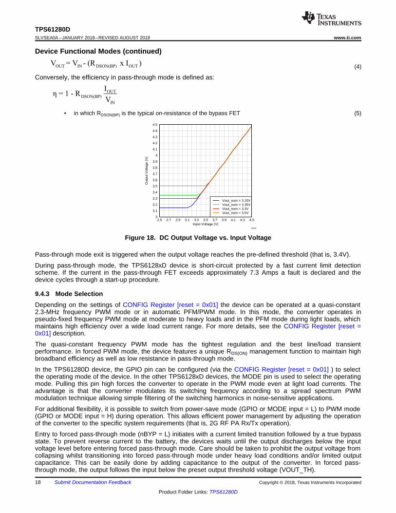
3
3.1
3.2
3.3
3.4
3.5
3.6
3.7
3.8
3.9
4
4.1
4.2
4.3
4.4
4.5
2.5 2.7 2.9 3.1 3.3 3.5 3.7 3.9 4.1 4.3 4.5Input Voltage (V)
Out
put V
olta
ge (
V)
Vout_nom = 3.15VVout_nom = 3.35VVout_nom = 3.3VVout_nom = 3.5V
G000
OUTDSON(BP)
IN
Iη = 1 - R
V
OUT IN DSON(BP) OUTV = V - (R x I )
18
TPS61280DSLVSEA0A –JANUARY 2018–REVISED AUGUST 2018 www.ti.com
Product Folder Links: TPS61280D
Submit Documentation Feedback Copyright © 2018, Texas Instruments Incorporated
Device Functional Modes (continued)
(4)
Conversely, the efficiency in pass-through mode is defined as:
• in which RDSON(BP) is the typical on-resistance of the bypass FET (5)
Figure 18. DC Output Voltage vs. Input Voltage
Pass-through mode exit is triggered when the output voltage reaches the pre-defined threshold (that is, 3.4V).
During pass-through mode, the TPS6128xD device is short-circuit protected by a fast current limit detectionscheme. If the current in the pass-through FET exceeds approximately 7.3 Amps a fault is declared and thedevice cycles through a start-up procedure.
9.4.3 Mode SelectionDepending on the settings of CONFIG Register [reset = 0x01] the device can be operated at a quasi-constant2.3-MHz frequency PWM mode or in automatic PFM/PWM mode. In this mode, the converter operates inpseudo-fixed frequency PWM mode at moderate to heavy loads and in the PFM mode during light loads, whichmaintains high efficiency over a wide load current range. For more details, see the CONFIG Register [reset =0x01] description.
The quasi-constant frequency PWM mode has the tightest regulation and the best line/load transientperformance. In forced PWM mode, the device features a unique RDS(ON) management function to maintain highbroadband efficiency as well as low resistance in pass-through mode.
In the TPS61280D device, the GPIO pin can be configured (via the CONFIG Register [reset = 0x01] ) to selectthe operating mode of the device. In the other TPS6128xD devices, the MODE pin is used to select the operatingmode. Pulling this pin high forces the converter to operate in the PWM mode even at light load currents. Theadvantage is that the converter modulates its switching frequency according to a spread spectrum PWMmodulation technique allowing simple filtering of the switching harmonics in noise-sensitive applications.
For additional flexibility, it is possible to switch from power-save mode (GPIO or MODE input = L) to PWM mode(GPIO or MODE input = H) during operation. This allows efficient power management by adjusting the operationof the converter to the specific system requirements (that is, 2G RF PA Rx/Tx operation).
Entry to forced pass-through mode (nBYP = L) initiates with a current limited transition followed by a true bypassstate. To prevent reverse current to the battery, the devices waits until the output discharges below the inputvoltage level before entering forced pass-through mode. Care should be taken to prohibit the output voltage fromcollapsing whilst transitioning into forced pass-through mode under heavy load conditions and/or limited outputcapacitance. This can be easily done by adding capacitance to the output of the converter. In forced pass-through mode, the output follows the input below the preset output threshold voltage (VOUT_TH).
f
D
L
VΔI
INL ×=
IVALLEY
IL
f
IPEAK
RectifierCurrent
IOUT(DC)
InductorCurrent
IncreasedLoad Current
IIN(DC)
IIN(DC)
Current LimitThreshold
IOUTDIL
DIL
f
D´=D
L
VI
IN
L
h´´=
O U T
I N)O U T ( M A X _ D C
V
VI
L I M I TI
19
TPS61280Dwww.ti.com SLVSEA0A –JANUARY 2018–REVISED AUGUST 2018
Product Folder Links: TPS61280D
Submit Documentation FeedbackCopyright © 2018, Texas Instruments Incorporated
Device Functional Modes (continued)9.4.4 Current Limit OperationThe TPS6128xD device features a valley inductor current limit scheme.
In dc/dc boost mode, the TPS6128xD device employs a current limit detection scheme in which the voltage dropacross the synchronous rectifier is sensed during the off-time. In the TPS61280D the current limit threshold canbe set via an I2C register. TPS6128xD devices have a fixed current limit threshold. See Device ComparisonTable for detailed information.
The output voltage is reduced as the power stage of the device operates in a constant current mode. Themaximum continuous output current (IOUT(MAX)), before entering current limit (CL) operation, can be defined byEquation 6.
where• η is the efficiency• The inductor peak-to-peak current ripple (ΔIL) is calculated by Equation 7 (6)
(7)
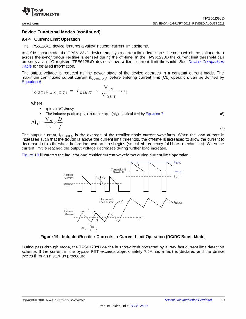
The output current, IOUT(DC), is the average of the rectifier ripple current waveform. When the load current isincreased such that the trough is above the current limit threshold, the off-time is increased to allow the current todecrease to this threshold before the next on-time begins (so called frequency fold-back mechanism). When thecurrent limit is reached the output voltage decreases during further load increase.
Figure 19 illustrates the inductor and rectifier current waveforms during current limit operation.
Figure 19. Inductor/Rectifier Currents in Current Limit Operation (DC/DC Boost Mode)
During pass-through mode, the TPS6128xD device is short-circuit protected by a very fast current limit detectionscheme. If the current in the bypass FET exceeds approximately 7.5Amps a fault is declared and the devicecycles through a start-up procedure.
20
TPS61280DSLVSEA0A –JANUARY 2018–REVISED AUGUST 2018 www.ti.com
Product Folder Links: TPS61280D
Submit Documentation Feedback Copyright © 2018, Texas Instruments Incorporated
Device Functional Modes (continued)9.4.5 Start-Up and Shutdown ModeThe TPS6128xD automatically powers-up as soon as the input voltage is applied. The device has an internalsoft-start circuit that limits the inrush current during start-up. The first phase in the start-up procedure is to biasthe output node close to the input level (so called pre-charge phase).
In this operating mode, the device limits its output current to ca. 500mA. Should the output voltage not havereached the input level within a maximum duration of 750µs, the device automatically increases its pre-chargecurrent to ca. 2000mA. If the output voltage still fails to reach its target after 1.5ms, a fault condition is declared.After waiting 1ms, a restart is attempted.
When output voltage being close to Vout, the device enters into boost startup mode (for Auto Mode only). Thedevice provides a reduced current limit of ~1.25A (I2C programable for TPS61280D to set it back to normalcurrent limit) when the output voltage is below pre-set voltage to avoid the high inrush current from battery.
During start-up, it is recommended to keep DC load current draw below 250mA.
The TPS6128xD device contains a thermal regulation loop that monitors the die temperature during the pre-charge phase. If the die temperature rises to high values of about 110°C, the device automatically reduces thecurrent to prevent the die temperature from increasing further. Once the die temperature drops about 10°C belowthe threshold, the device will automatically increase the current to the target value. This function also reduces thecurrent during a short-circuit condition.
When the EN and nBYP pins are set high, the device enters normal operation (that is, automatic dc/dc boost,pass-through mode) and ensures that the output voltage remains above a pre-defined threshold (that is, 3.3 V).
Setting the EN pin low (nBYP = 1) forces the TPS6128xD device in shutdown mode with a current consumptionof <8.5 µA typical. In this mode, the output of the converter is regulated to a minimum level so as to limit theinput-to-output voltage difference to less than 3.6 V (typical). The device is capable of sinking up to 10 mA outputcurrent and prohibits reverse current flow from the output to the input. For proper operation, the EN pin must beterminated and must not be left floating.
Changing operating mode from auto mode (EN = nBYP = 1) to low IQ Pass-through mode (EN = nBYP = 0) withdevice pins EN and nBYP can either be done controlling EN and nBYP pins from same control signal (delaybetween signal < 60ns) or first switching in forced pass-through mode (EN = 1, nBYP = 0) followed by switchingto low IQ Pass-through mode (EN = nBYP = 0).
The TPS6128xD device also features the possibility of shutting the converter output for a short period of time,either via the nRST/nFAULT (GPIO). Pulling this input low initiates a reset of the converter's output. Thesequence is falling edge-triggered and consists of a discharge phase (down to ca. 600 mV or lower) of thecapacitance located at the converter's output followed by a start-up phase.
Table 2. Mode of OperationEN Input nBYP Input Device State
0 0 The device is shut down in pass-through mode featuring a shutdown current down to ca. 3µA typ.The load current capability is limited (up to ca. 250mA).
0 1 The device is shut down and the output voltage is reduced to a minimum value (VIN - VOUT ≤ 3.6V).The device shutdown current is approximately 8.5µA typ.
1 0The device is active in forced pass-through mode.The device supply current is approximately 15µA typ. from the battery. The device is short circuit protectedby a current limit of ca.7300mA.
1 1 The device is active in auto mode (dc/dc boost, pass-through).The device supply current is approximately 50µA typ. from the battery.
9.4.6 Undervoltage LockoutThe under voltage lockout circuit prevents the device from malfunctioning at low input voltages and the batteryfrom excessive discharge. The I2C control interface and the output stage of the converter are disabled once thefalling VIN trips the under-voltage lockout threshold VUVLO (2 V typical). The device starts operation once therising VIN trips VUVLO threshold plus its hysteresis of 100 mV at typ. 2.1 V.
21
TPS61280Dwww.ti.com SLVSEA0A –JANUARY 2018–REVISED AUGUST 2018
Product Folder Links: TPS61280D
Submit Documentation FeedbackCopyright © 2018, Texas Instruments Incorporated
9.4.7 Thermal ShutdownAs soon as the junction temperature, TJ, exceeds 160°C (typ.) the device goes into thermal shutdown. In thismode the bypass, high-side and low-side MOSFETs are turned-off. When the junction temperature falls belowthe thermal shutdown minus its hysteresis, the device continuous the operation.
9.4.8 Fault State and Power-GoodThe TPS6128xD enters the fault state under any of the followings conditions:
• The output voltage fails to achieve the required level during a start-up phase.• The output voltage falls out of regulation (in pre-charge mode).• The device has entered thermal shutdown.
Once a fault is triggered, the regulator stops operating and disconnects the load. After waiting 1ms, the deviceattempts to restart. The TPS61280D device can be configured to signal a fault condition by pulling the open-drainGPIO pin (nFAULT) low for a short period of time. The nFAULT output provides a falling edge triggered interruptsignal to the host. To ensure proper operation, the GPIO port needs to be pull high quick enough, that is, fasterthan ca. 200ns. To do so, it is recommended to use a GPIO pull-up resistor in the range of 1kΩ to 10kΩ.
The TPS6128xD (simple logic I/F version) device only provide a power-good output (PG) for signaling the systemwhen the regulator has successfully completed start-up and no faults have occurred. Power-good also functionsas an early warning flag for excessive die temperature and overload conditions.
• PG is asserted high when the start-up sequence is successfully completed.• PG is pulled low when the output voltage falls approximately 10% below its regulation level or the die
temperature exceeds 115°C. PG is re-asserted high when the device cools below ca. 100°C.• Any fault condition causes PG to be de-asserted.• PG is pulled high when the device is operating in forced pass-through mode (that is, nBYP = L).• PG is pulled high when the device is in shutdown mode.
Data linestable;
data valid
DATA
CLK
Changeof dataallowed
START Condition
DATA
CLK
STOP Condition
S P
22
TPS61280DSLVSEA0A –JANUARY 2018–REVISED AUGUST 2018 www.ti.com
Product Folder Links: TPS61280D
Submit Documentation Feedback Copyright © 2018, Texas Instruments Incorporated
9.5 Programming
9.5.1 Serial Interface Description (TPS61280D)I2C™ is a 2-wire serial interface developed by Philips Semiconductor, now NXP Semiconductors (see I2C-BusSpecification, Version 2.1, January 2000). The bus consists of a data line (SDA) and a clock line (SCL) with pull-up structures. When the bus is idle, both SDA and SCL lines are pulled high. All the I2C compatible devicesconnect to the I2C bus through open drain I/O pins, SDA and SCL. A master device, usually a microcontroller ora digital signal processor, controls the bus. The master is responsible for generating the SCL signal and deviceaddresses. The master also generates specific conditions that indicate the START and STOP of data transfer. Aslave device receives and/or transmits data on the bus under control of the master device.
The TPS6128xD device works as a slave and supports the following data transfer modes, as defined in the I2C-Bus Specification: standard mode (100 kbps) and fast mode (400 kbps), fast mode plus (1 Mbps) and high-speedmode (3.4 Mbps). The interface adds flexibility to the power supply solution, enabling most functions to beprogrammed to new values depending on the instantaneous application requirements. Register contents remainintact as long as supply voltage remains above 2.1V.
The data transfer protocol for standard and fast modes is exactly the same, therefore they are referred to as F/S-mode in this document. The protocol for high-speed mode is different from F/S-mode, and it is referred to as HS-mode. The TPS6128xD device supports 7-bit addressing; 10-bit addressing and general call address are notsupported. The device 7bit address is defined as ‘111 0101’.
It is recommended that the I2C masters initiates a STOP condition on the I2C bus after the initial power up ofSDA and SCL pull-up voltages to ensure reset of the TPS6128xD I2C engine.
9.5.2 Standard-, Fast-, Fast-Mode Plus ProtocolThe master initiates data transfer by generating a start condition. The start condition is when a high-to-lowtransition occurs on the SDA line while SCL is high, as shown in Figure 20. All I2C-compatible devices shouldrecognize a start condition.
Figure 20. START and STOP Conditions
The master then generates the SCL pulses, and transmits the 7-bit address and the read/write direction bit R/Won the SDA line. During all transmissions, the master ensures that data is valid. A valid data condition requiresthe SDA line to be stable during the entire high period of the clock pulse (see Figure 21). All devices recognizethe address sent by the master and compare it to their internal fixed addresses. Only the slave device with amatching address generates an acknowledge (see Figure 22) by pulling the SDA line low during the entire highperiod of the ninth SCL cycle. Upon detecting this acknowledge, the master knows that communication link with aslave has been established.
Figure 21. Bit Transfer on the Serial Interface
23
TPS61280Dwww.ti.com SLVSEA0A –JANUARY 2018–REVISED AUGUST 2018
Product Folder Links: TPS61280D
Submit Documentation FeedbackCopyright © 2018, Texas Instruments Incorporated
Programming (continued)The master generates further SCL cycles to either transmit data to the slave (R/W bit 1) or receive data from theslave (R/W bit 0). In either case, the receiver needs to acknowledge the data sent by the transmitter. So anacknowledge signal can either be generated by the master or by the slave, depending on which one is thereceiver. 9-bit valid data sequences consisting of 8-bit data and 1-bit acknowledge can continue as long asnecessary.
To signal the end of the data transfer, the master generates a stop condition by pulling the SDA line from low tohigh while the SCL line is high (see Figure 20). This releases the bus and stops the communication link with theaddressed slave. All I2C compatible devices must recognize the stop condition. Upon the receipt of a stopcondition, all devices know that the bus is released, and they wait for a start condition followed by a matchingaddress.
Attempting to read data from register addresses not listed in this section will result in 00h being read out.
Figure 22. Acknowledge on the I2C Bus
Figure 23. Bus Protocol
Slave Address R/W A Register Address A PSr
1 7 1 1 1 18
Data
8
A/A
1
HS-Master Code A
1 18
F/S Mode HS Mode F/S Mode
Data Transferred
(n x Bytes + Acknowledge)HS Mode Continues
From Master to TPS6128xD
From TPS6128xD to Master
A = Acknowledge (SDA low)= Not acknowledge (SDA high)
S = START conditionSr = REPEATED START conditionP = STOP condition
A
Slave AddressSr
S
Slave Address R/W A Register Address A Data PS
1 7 1 1 1 1 18 8
“0” Write
Sr
1
Slave Address R/W
7 1
“1” Read
A
1
From Master to TPS6128xD
From TPS6128xD to Master
A/A
A = Acknowledge (SDA low)= Not acknowledge (SDA high)
S = START conditionSr = REPEATED START conditionP = STOP condition
A
Slave Address R/W A Register Address A Data A/A PS
1 7 1 1 1 1 18 8
“0” Write
From Master to TPS6128xD
From TPS6128xD to Master
A = Acknowledge (SDA low)= Not acknowledge (SDA high)
S = START conditionSr = REPEATED START conditionP = STOP condition
A
24
TPS61280DSLVSEA0A –JANUARY 2018–REVISED AUGUST 2018 www.ti.com
Product Folder Links: TPS61280D
Submit Documentation Feedback Copyright © 2018, Texas Instruments Incorporated
Programming (continued)9.5.3 HS-Mode ProtocolThe master generates a start condition followed by a valid serial byte containing HS master code 00001XXX.This transmission is made in F/S-mode at no more than 400 Kbps. No device is allowed to acknowledge the HSmaster code, but all devices must recognize it and switch their internal setting to support 3.4 Mbps operation.
The master then generates a repeated start condition (a repeated start condition has the same timing as the startcondition). After this repeated start condition, the protocol is the same as F/S-mode, except that transmissionspeeds up to 3.4 Mbps are allowed. A stop condition ends the HS-mode and switches all the internal settings ofthe slave devices to support the F/S-mode. Instead of using a stop condition, repeated start conditions should beused to secure the bus in HS-mode.
Attempting to read data from register addresses not listed in this section will result in 00h being read out.
9.5.4 TPS6128xD I2C Update SequenceThe TPS6128xD requires a start condition, a valid I2C address, a register address byte, and a data byte for asingle update. After the receipt of each byte, TPS6128xD device acknowledges by pulling the SDA line lowduring the high period of a single clock pulse. A valid I2C address selects the TPS6128xD. TPS6128xD performsan update on the falling edge of the acknowledge signal that follows the LSB byte.
Figure 24. : “Write” Data Transfer Format in Standard-, Fast, Fast-Plus Modes
Figure 25. “Read” Data Transfer Format in Standard-, Fast, Fast-Plus Modes
Figure 26. Data Transfer Format in H/S-Mode
25
TPS61280Dwww.ti.com SLVSEA0A –JANUARY 2018–REVISED AUGUST 2018
Product Folder Links: TPS61280D
Submit Documentation FeedbackCopyright © 2018, Texas Instruments Incorporated
9.6 Register Maps
9.6.1 Slave Address Byte
MSB LSB1 1 1 0 1 A1 A0
The slave address byte is the first byte received following the START condition from the master device.
9.6.2 Register Address Byte
MSB LSB0 0 0 0 0 D2 D1 D0
Following the successful acknowledgment of the slave address, the bus master will send a byte to theTPS6128xD, which will contain the address of the register to be accessed.
9.6.3 I2C Registers, E2PROM, Write ProtectConfiguration parameters can be changed by writing the desired values to the appropriate I2C register(s). TheI2C registers are volatile and their contents are lost when power is removed from the device. By writing to theE2PROMCTRL Register [reset = 0xFF], it is possible to store the active configuration in non-volatile E2PROM;during power-up, the contents of the E2PROM are copied into the I2C registers and used to configure the device.
NOTEAn active high Write Protect (WP) bit prevents the configuration parameters from beingchanged by accident. Once the E2PROM memory has been programmed with WriteProtect (WP) bit set, its content will be locked and can not be reprogrammed any more.
Configuration parameters can be read from the I2C register(s) or E2PROM registers at any time (the WP bit hasno effect on read operations).
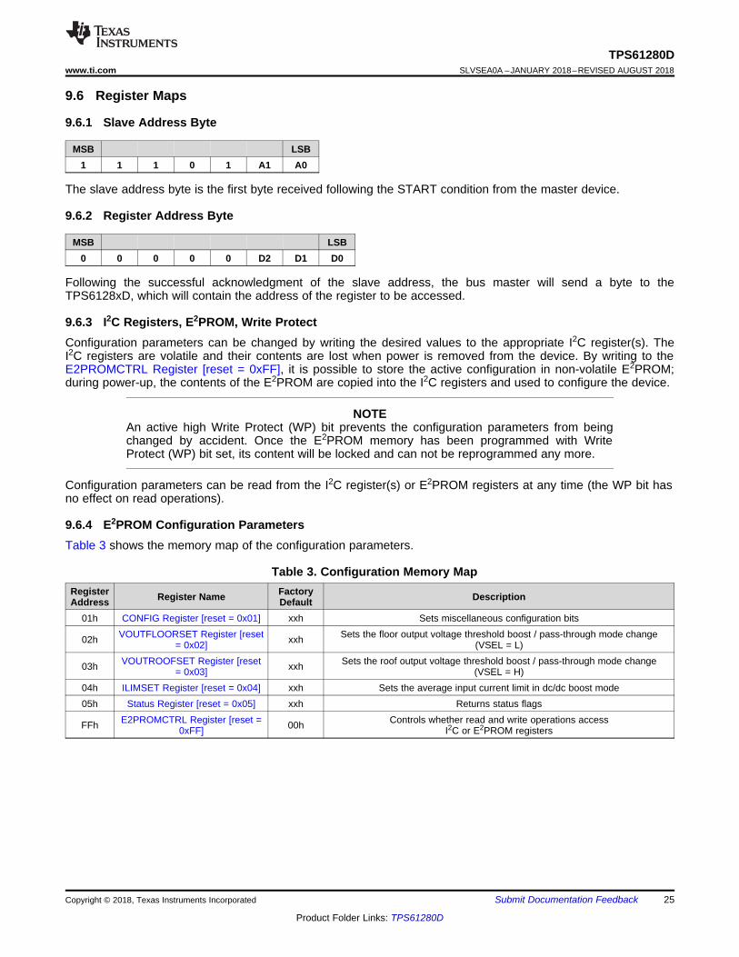
9.6.4 E2PROM Configuration ParametersTable 3 shows the memory map of the configuration parameters.
Table 3. Configuration Memory MapRegisterAddress Register Name Factory
Default Description
01h CONFIG Register [reset = 0x01] xxh Sets miscellaneous configuration bits
02h VOUTFLOORSET Register [reset= 0x02] xxh Sets the floor output voltage threshold boost / pass-through mode change
(VSEL = L)
03h VOUTROOFSET Register [reset= 0x03] xxh Sets the roof output voltage threshold boost / pass-through mode change
(VSEL = H)04h ILIMSET Register [reset = 0x04] xxh Sets the average input current limit in dc/dc boost mode05h Status Register [reset = 0x05] xxh Returns status flags
FFh E2PROMCTRL Register [reset =0xFF] 00h Controls whether read and write operations access
I2C or E2PROM registers
S 0 A A7-Bit Slave Address Control Register Address Control Register Data A
EAh
P
FFh C0h
26
TPS61280DSLVSEA0A –JANUARY 2018–REVISED AUGUST 2018 www.ti.com
Product Folder Links: TPS61280D
Submit Documentation Feedback Copyright © 2018, Texas Instruments Incorporated
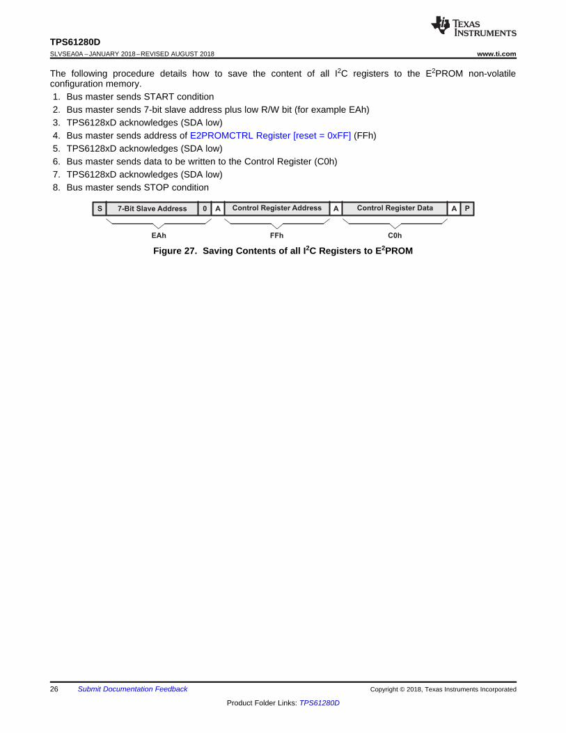
The following procedure details how to save the content of all I2C registers to the E2PROM non-volatileconfiguration memory.1. Bus master sends START condition2. Bus master sends 7-bit slave address plus low R/W bit (for example EAh)3. TPS6128xD acknowledges (SDA low)4. Bus master sends address of E2PROMCTRL Register [reset = 0xFF] (FFh)5. TPS6128xD acknowledges (SDA low)6. Bus master sends data to be written to the Control Register (C0h)7. TPS6128xD acknowledges (SDA low)8. Bus master sends STOP condition
Figure 27. Saving Contents of all I2C Registers to E2PROM
27
TPS61280Dwww.ti.com SLVSEA0A –JANUARY 2018–REVISED AUGUST 2018
Product Folder Links: TPS61280D
Submit Documentation FeedbackCopyright © 2018, Texas Instruments Incorporated
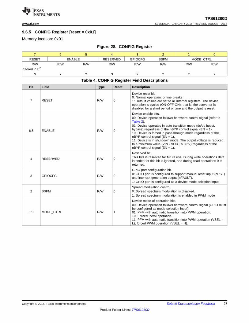
9.6.5 CONFIG Register [reset = 0x01]Memory location: 0x01
Figure 28. CONFIG Register
7 6 5 4 3 2 1 0RESET ENABLE RESERVED GPIOCFG SSFM MODE_CTRL
R/W R/W R/W R/W R/W R/W R/W R/WStored in E2
N Y Y N Y Y Y Y
Table 4. CONFIG Register Field DescriptionsBit Field Type Reset Description
7 RESET R/W 0
Device reset bit.0: Normal operation. or line breaks1: Default values are set to all internal registers. The deviceoperation is cycled (ON-OFF-ON), that is, the converter isdisabled for a short period of time and the output is reset.
6:5 ENABLE R/W 0
Device enable bits.00: Device operation follows hardware control signal (refer toTable 2).01: Device operates in auto transition mode (dc/dc boost,bypass) regardless of the nBYP control signal (EN = 1).10: Device is forced in pass-through mode regardless of thenBYP control signal (EN = 1).11: Device is in shutdown mode. The output voltage is reducedto a minimum value (VIN - VOUT ≤ 3.6V) regardless of thenBYP control signal (EN = 1).
4 RESERVED R/W 0
Reserved bit.This bits is reserved for future use. During write operations dataintended for this bit is ignored, and during read operations 0 isreturned.
3 GPIOCFG R/W 0
GPIO port configuration bit.0: GPIO port is configured to support manual reset input (nRST)and interrupt generation output (nFAULT).1: GPIO port is configured as a device mode selection input.
2 SSFM R/W 0Spread modulation control.0: Spread spectrum modulation is disabled.1: Spread spectrum modulation is enabled in PWM mode
1:0 MODE_CTRL R/W 1
Device mode of operation bits.00: Device operation follows hardware control signal (GPIO mustbe configured as mode selection input).01: PFM with automatic transition into PWM operation.10: Forced PWM operation.11: PFM with automatic transition into PWM operation (VSEL =L), forced PWM operation (VSEL = H).
28
TPS61280DSLVSEA0A –JANUARY 2018–REVISED AUGUST 2018 www.ti.com
Product Folder Links: TPS61280D
Submit Documentation Feedback Copyright © 2018, Texas Instruments Incorporated
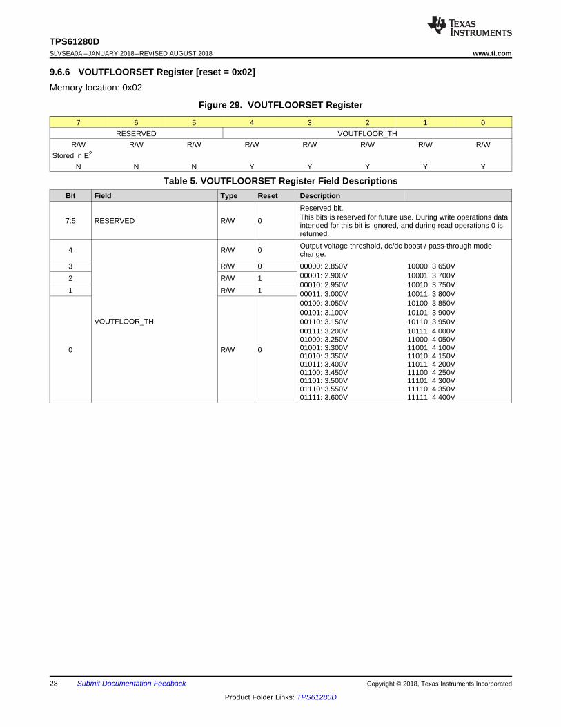
9.6.6 VOUTFLOORSET Register [reset = 0x02]Memory location: 0x02
Figure 29. VOUTFLOORSET Register
7 6 5 4 3 2 1 0RESERVED VOUTFLOOR_TH
R/W R/W R/W R/W R/W R/W R/W R/WStored in E2
N N N Y Y Y Y Y
Table 5. VOUTFLOORSET Register Field DescriptionsBit Field Type Reset Description
7:5 RESERVED R/W 0
Reserved bit.This bits is reserved for future use. During write operations dataintended for this bit is ignored, and during read operations 0 isreturned.
4
VOUTFLOOR_TH
R/W 0 Output voltage threshold, dc/dc boost / pass-through modechange.
3 R/W 0 00000: 2.850V00001: 2.900V00010: 2.950V00011: 3.000V00100: 3.050V00101: 3.100V00110: 3.150V00111: 3.200V01000: 3.250V01001: 3.300V01010: 3.350V01011: 3.400V01100: 3.450V01101: 3.500V01110: 3.550V01111: 3.600V
10000: 3.650V10001: 3.700V10010: 3.750V10011: 3.800V10100: 3.850V10101: 3.900V10110: 3.950V10111: 4.000V11000: 4.050V11001: 4.100V11010: 4.150V11011: 4.200V11100: 4.250V11101: 4.300V11110: 4.350V11111: 4.400V
2 R/W 11 R/W 1
0 R/W 0
29
TPS61280Dwww.ti.com SLVSEA0A –JANUARY 2018–REVISED AUGUST 2018
Product Folder Links: TPS61280D
Submit Documentation FeedbackCopyright © 2018, Texas Instruments Incorporated
9.6.7 VOUTROOFSET Register [reset = 0x03]Memory location: 0x03
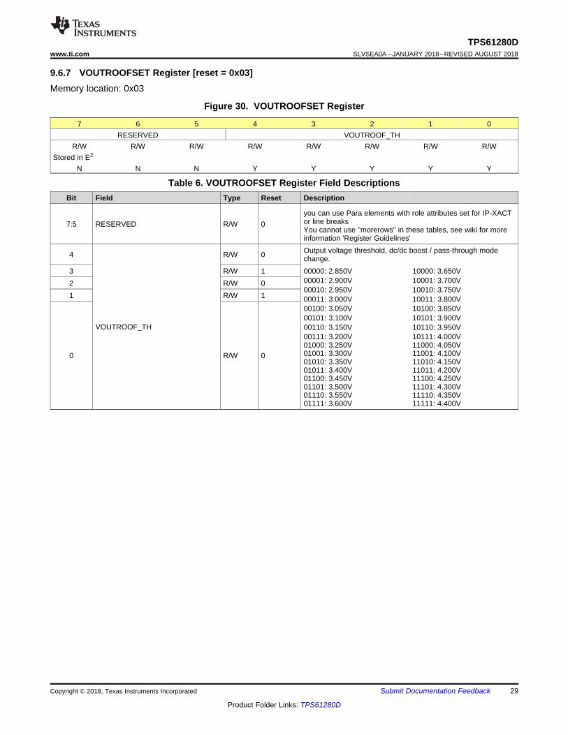
Figure 30. VOUTROOFSET Register
7 6 5 4 3 2 1 0RESERVED VOUTROOF_TH
R/W R/W R/W R/W R/W R/W R/W R/WStored in E2
N N N Y Y Y Y Y
Table 6. VOUTROOFSET Register Field DescriptionsBit Field Type Reset Description
7:5 RESERVED R/W 0you can use Para elements with role attributes set for IP-XACTor line breaksYou cannot use "morerows" in these tables, see wiki for moreinformation 'Register Guidelines'
4
VOUTROOF_TH
R/W 0 Output voltage threshold, dc/dc boost / pass-through modechange.
3 R/W 1 00000: 2.850V00001: 2.900V00010: 2.950V00011: 3.000V00100: 3.050V00101: 3.100V00110: 3.150V00111: 3.200V01000: 3.250V01001: 3.300V01010: 3.350V01011: 3.400V01100: 3.450V01101: 3.500V01110: 3.550V01111: 3.600V
10000: 3.650V10001: 3.700V10010: 3.750V10011: 3.800V10100: 3.850V10101: 3.900V10110: 3.950V10111: 4.000V11000: 4.050V11001: 4.100V11010: 4.150V11011: 4.200V11100: 4.250V11101: 4.300V11110: 4.350V11111: 4.400V
2 R/W 01 R/W 1
0 R/W 0
30
TPS61280DSLVSEA0A –JANUARY 2018–REVISED AUGUST 2018 www.ti.com
Product Folder Links: TPS61280D
Submit Documentation Feedback Copyright © 2018, Texas Instruments Incorporated
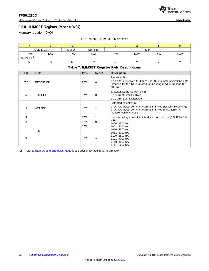
9.6.8 ILIMSET Register [reset = 0x04]Memory location: 0x04
Figure 31. ILIMSET Register
7 6 5 4 3 2 1 0RESERVED ILIM OFF Soft-start ILIM
R/W R/W R/W R/W R/W R/W R/W R/WStored in E2
N N N Y Y Y Y Y
(1) Refer to Start-Up and Shutdown Mode Mode section for additional information.
Table 7. ILIMSET Register Field DescriptionsBit Field Type Reset Description
7:6 RESERVED R/W 0
Reserved bit.This bits is reserved for future use. During write operations dataintended for this bit is ignored, and during read operations 0 isreturned.
5 ILIM OFF R/W 0Enable/Disable Current Limit0 : Current Limit Enabled1 : Current Limit Disabled
4 Soft-start R/W 1
Soft-start selection bit.0: DC/DC boost soft-start current is limited per ILIM bit settings1: DC/DC boost soft-start current is limited to ca. 1250mAinductor valley current
3
ILIM
R/W 1 Inductor valley current limit in dc/dc boost mode (COUTRNG bit= 0) (1).1000: 1500mA1001: 2000mA1010: 2500mA1011: 3000mA1100: 3500mA1101: 4000mA1110: 4500mA1111: 5000mA
2 R/W 01 R/W 1
0 R/W 1
31
TPS61280Dwww.ti.com SLVSEA0A –JANUARY 2018–REVISED AUGUST 2018
Product Folder Links: TPS61280D
Submit Documentation FeedbackCopyright © 2018, Texas Instruments Incorporated
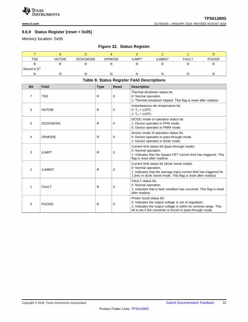
9.6.9 Status Register [reset = 0x05]Memory location: 0x05
Figure 32. Status Register
7 6 5 4 3 2 1 0TSD HOTDIE DCDCMODE OPMODE ILIMPT ILIMBST FAULT PGOOD
R R R R R R R RStored in E2
N N N N N N N N
Table 8. Status Register Field DescriptionsBit Field Type Reset Description
7 TSD R 0Thermal shutdown status bit.0: Normal operation.1: Thermal shutdown tripped. This flag is reset after readout.
6 HOTDIE R 0Instantaneous die temperature bit.0: TJ < 115ºC.1: TJ > 115ºC.
5 DCDCMODE R 0DC/DC mode of operation status bit.1: Device operates in PFM mode.0: Device operates in PWM mode.
4 OPMODE R 0Device mode of operation status bit.0: Device operates in pass-through mode.1: Device operates in dc/dc mode.
3 ILIMPT R 0
Current limit status bit (pass-through mode).0: Normal operation.1: Indicates that the bypass FET current limit has triggered. Thisflag is reset after readout.
2 ILIMBST R 0
Current limit status bit (dc/dc boost mode).0: Normal operation.1: Indicates that the average input current limit has triggered for1.5ms in dc/dc boost mode. This flag is reset after readout.
1 FAULT R 0
FAULT status bit.0: Normal operation.1: Indicates that a fault condition has occurred. This flag is resetafter readout.
0 PGOOD R 0
Power Good status bit.0: Indicates the output voltage is out of regulation.1: Indicates the output voltage is within its nominal range. Thisbit is set if the converter is forced in pass-through mode.
32
TPS61280DSLVSEA0A –JANUARY 2018–REVISED AUGUST 2018 www.ti.com
Product Folder Links: TPS61280D
Submit Documentation Feedback Copyright © 2018, Texas Instruments Incorporated
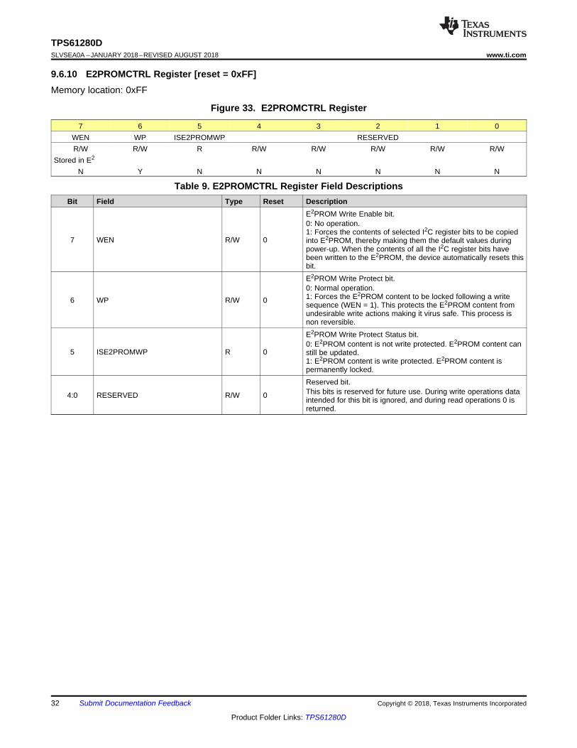
9.6.10 E2PROMCTRL Register [reset = 0xFF]Memory location: 0xFF
Figure 33. E2PROMCTRL Register
7 6 5 4 3 2 1 0WEN WP ISE2PROMWP RESERVEDR/W R/W R R/W R/W R/W R/W R/W
Stored in E2
N Y N N N N N N
Table 9. E2PROMCTRL Register Field DescriptionsBit Field Type Reset Description
7 WEN R/W 0
E2PROM Write Enable bit.0: No operation.1: Forces the contents of selected I2C register bits to be copiedinto E2PROM, thereby making them the default values duringpower-up. When the contents of all the I2C register bits havebeen written to the E2PROM, the device automatically resets thisbit.
6 WP R/W 0
E2PROM Write Protect bit.0: Normal operation.1: Forces the E2PROM content to be locked following a writesequence (WEN = 1). This protects the E2PROM content fromundesirable write actions making it virus safe. This process isnon reversible.
5 ISE2PROMWP R 0
E2PROM Write Protect Status bit.0: E2PROM content is not write protected. E2PROM content canstill be updated.1: E2PROM content is write protected. E2PROM content ispermanently locked.
4:0 RESERVED R/W 0
Reserved bit.This bits is reserved for future use. During write operations dataintended for this bit is ignored, and during read operations 0 isreturned.
33
TPS61280Dwww.ti.com SLVSEA0A –JANUARY 2018–REVISED AUGUST 2018
Product Folder Links: TPS61280D
Submit Documentation FeedbackCopyright © 2018, Texas Instruments Incorporated
10 Application and Implementation
NOTEInformation in the following applications sections is not part of the TI componentspecification, and TI does not warrant its accuracy or completeness. TI’s customers areresponsible for determining suitability of components for their purposes. Customers shouldvalidate and test their design implementation to confirm system functionality.
10.1 Application InformationThe devices are step up dc/dc converters with true bypass function integrated. They are typically used aspreregulators with input voltage ranges from 2.3V to 4.8V, extend the battery run time and overcome inputcurrent and input voltage limitations of the system being powered.
While the input voltage higher than boost/bypass threshold, the high-efficient integrated pass-through pathconnects the battery to the powered system directly.
If the input voltage becomes lower than boost/bypass threshold, the device seamlessly transitions into boostmode operation with a maximum available output current of 3 A.
The following design procedure can be used to select component values for the TPS61281D and TPS61282D(also applicable for TPS61280D just by I2C program).
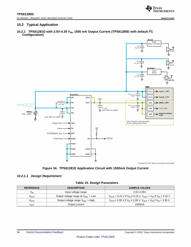
VBAT’
PMIC
eMMC, 2.95V
LCD, 2.80V
Antenna switches2.60V
C
10 FDECOUPLING
µ
Vcore1, 1.05V
Vcore2, 1.15V
C
10 FDECOUPLING
µ
WIFI PA
WL8PM27
C
4.7 FIN
µ
SMPS
SMPS
SuPABUCK
PMIC
eMMC, 2.95V
Note: Resistive load equivalentfor the measurement result.
Antenna switches2.60V
Vcore1, 1.05V
Vcore2, 1.15V
WIFI PA
SMPS
SMPS
SuPABUCK
LDOLDO
LDOLDO
LDOLDO
Battery
2.7V .. 4.35V
Battery
200 to 600mV
2.7V
3G PA
LM3242
C
10 µFIN
SuPABUCK / BYPASS
C
1.5µF X5R 6.3V (0402)I
C (x2)
10µF X5R 6.3V (0603)O
L
0.47 μH
SW
SW
VIN
VIN
VSEL
BYP
MODE
PGND
PGND
PGND
EN
VOUT
VOUT
PG
AGND
AGND
Enable 1.8V
Interrupt
Forced Bypass / Auto
Voltage Select
PFM/FPWM
TPS61281D
C
4.7 FIN
µ2G PA
Copyright © 2016, Texas Instruments Incorporated
34
TPS61280DSLVSEA0A –JANUARY 2018–REVISED AUGUST 2018 www.ti.com
Product Folder Links: TPS61280D
Submit Documentation Feedback Copyright © 2018, Texas Instruments Incorporated
10.2 Typical Application
10.2.1 TPS61281D with 2.5V-4.35 VIN, 1500 mA Output Current (TPS61280D with default I2CConfiguration)
Figure 34. TPS61281D Application Circuit with 1500mA Output Current
10.2.1.1 Design Requirement
Table 10. Design ParametersREFERENCE DESCRIPTION SAMPLE VALUES
VIN Input voltage range 2.5V-4.35VVOUT Output voltage range at VSEL = Low VOUT = 3.15 V if VIN ≤ 3.15 V, VOUT = VIN if VIN > 3.15 VVOUT Output voltage range VSEL = High VOUT= 3.35 V if VIN ≤ 3.35 V, VOUT = VIN if VIN > 3.35 VIOUT Output current 1500mA
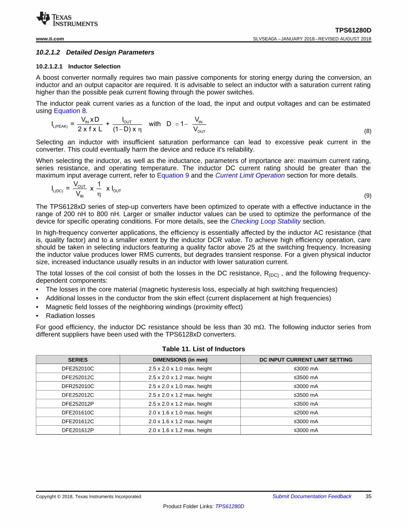
OUTL(DC) OUT
IN
V 1I = x x I
V h
OUTIN INL(PEAK)
OUT
IV xD VI = + with D 1
2 x f x L (1 D) x V= -
- h
35
TPS61280Dwww.ti.com SLVSEA0A –JANUARY 2018–REVISED AUGUST 2018
Product Folder Links: TPS61280D
Submit Documentation FeedbackCopyright © 2018, Texas Instruments Incorporated
10.2.1.2 Detailed Design Parameters
10.2.1.2.1 Inductor Selection
A boost converter normally requires two main passive components for storing energy during the conversion, aninductor and an output capacitor are required. It is advisable to select an inductor with a saturation current ratinghigher than the possible peak current flowing through the power switches.
The inductor peak current varies as a function of the load, the input and output voltages and can be estimatedusing Equation 8.
(8)
Selecting an inductor with insufficient saturation performance can lead to excessive peak current in theconverter. This could eventually harm the device and reduce it's reliability.
When selecting the inductor, as well as the inductance, parameters of importance are: maximum current rating,series resistance, and operating temperature. The inductor DC current rating should be greater than themaximum input average current, refer to Equation 9 and the Current Limit Operation section for more details.
(9)
The TPS6128xD series of step-up converters have been optimized to operate with a effective inductance in therange of 200 nH to 800 nH. Larger or smaller inductor values can be used to optimize the performance of thedevice for specific operating conditions. For more details, see the Checking Loop Stability section.
In high-frequency converter applications, the efficiency is essentially affected by the inductor AC resistance (thatis, quality factor) and to a smaller extent by the inductor DCR value. To achieve high efficiency operation, careshould be taken in selecting inductors featuring a quality factor above 25 at the switching frequency. Increasingthe inductor value produces lower RMS currents, but degrades transient response. For a given physical inductorsize, increased inductance usually results in an inductor with lower saturation current.
The total losses of the coil consist of both the losses in the DC resistance, R(DC) , and the following frequency-dependent components:• The losses in the core material (magnetic hysteresis loss, especially at high switching frequencies)• Additional losses in the conductor from the skin effect (current displacement at high frequencies)• Magnetic field losses of the neighboring windings (proximity effect)• Radiation losses
For good efficiency, the inductor DC resistance should be less than 30 mΩ. The following inductor series fromdifferent suppliers have been used with the TPS6128xD converters.
Table 11. List of InductorsSERIES DIMENSIONS (in mm) DC INPUT CURRENT LIMIT SETTING
DFE252010C 2.5 x 2.0 x 1.0 max. height ≤3000 mADFE252012C 2.5 x 2.0 x 1.2 max. height ≤3500 mADFR252010C 2.5 x 2.0 x 1.0 max. height ≤3000 mADFE252012C 2.5 x 2.0 x 1.2 max. height ≤3500 mADFE252012P 2.5 x 2.0 x 1.2 max. height ≤3500 mADFE201610C 2.0 x 1.6 x 1.0 max. height ≤2000 mADFE201612C 2.0 x 1.6 x 1.2 max. height ≤3000 mADFE201612P 2.0 x 1.6 x 1.2 max. height ≤3000 mA
OUT LOUT(ESL) OUT
SW(FALL)
I ΔI 1ΔV = ESL x - - I x
1 - D 2 t
æ öç ÷è ø
OUT LOUT(ESL) OUT
SW(RISE)
I ΔI 1ΔV = ESL x + - I x
1 - D 2 t
æ öç ÷è ø
OUT LOUT(ESR)
I ΔIΔV = ESR x +
1 - D 2
æ öç ÷è ø
OUT OUT INMIN
OUT
I x (V - V )C =
f x V x VD
36
TPS61280DSLVSEA0A –JANUARY 2018–REVISED AUGUST 2018 www.ti.com
Product Folder Links: TPS61280D
Submit Documentation Feedback Copyright © 2018, Texas Instruments Incorporated
10.2.1.2.2 Output Capacitor
For the output capacitor, it is recommended to use small ceramic capacitors placed as close as possible to theVOUT and GND pins of the IC. If, for any reason, the application requires the use of large capacitors which cannot be placed close to the IC, using a smaller ceramic capacitor in parallel to the large one is highlyrecommended. This small capacitor should be placed as close as possible to the VOUT and GND pins of the IC.To get an estimate of the recommended minimum output capacitance, Equation 10 can be used.
where• f is the switching frequency which is 2.3 MHz (typ.) and ΔV is the maximum allowed output ripple. (10)
With a chosen ripple voltage of 20 mV, a minimum effective capacitance of 10 μF is needed. The total ripple islarger due to the ESR and ESL of the output capacitor. This additional component of the ripple can be calculatedusing Equation 11
(11)
(12)
where• IOUT = output current of the application• D = duty cycle• ΔIL = inductor ripple current• tSW(RISE) = switch node rise time• tSW(FALL) = switch node fall time• ESR = equivalent series resistance of the used output capacitor• ESL = equivalent series inductance of the used output capacitor (13)
An MLCC capacitor with twice the value of the calculated minimum should be used due to DC bias effects. Thisis required to maintain control loop stability. The output capacitor requires either an X7R or X5R dielectric. Y5Vand Z5U dielectric capacitors, aside from their wide variation in capacitance over temperature, become resistiveat high frequencies. There are no additional requirements regarding minimum ESR. Larger capacitors causelower output voltage ripple as well as lower output voltage drop during load transients.
In applications featuring high (pulsed) load currents (e.g. ≥ 2 Amps), it is recommended to run the converter witha reasonable amount of effective output capacitance and low-ESL device, for instance x2 22 µF X5R 6.3V (0603)MLCC capacitors connected in parallel with a 1 µF X5R 6.3 V (0306-2T) MLCC LL capacitor.
DC bias effect: high cap. ceramic capacitors exhibit DC bias effects, which have a strong influence on thedevice's effective capacitance. Therefore the right capacitor value has to be chosen very carefully. Package sizeand voltage rating in combination with material are responsible for differences between the rated capacitor valueand it's effective capacitance. For instance, a 10 µF X5R 6.3 V (0603) MLCC capacitor would typically show aneffective capacitance of less than 5 µF (under 3.5 V bias condition, high temperature).
For RF Power Amplifier applications, the output capacitor loading is combined between the dc/dc converter andthe RF Power Amplifier (x2 10 µF X5R 6.3 V (0603) + PA input cap 4.7 µF X5R 6.3 V (0402)) are recommended.
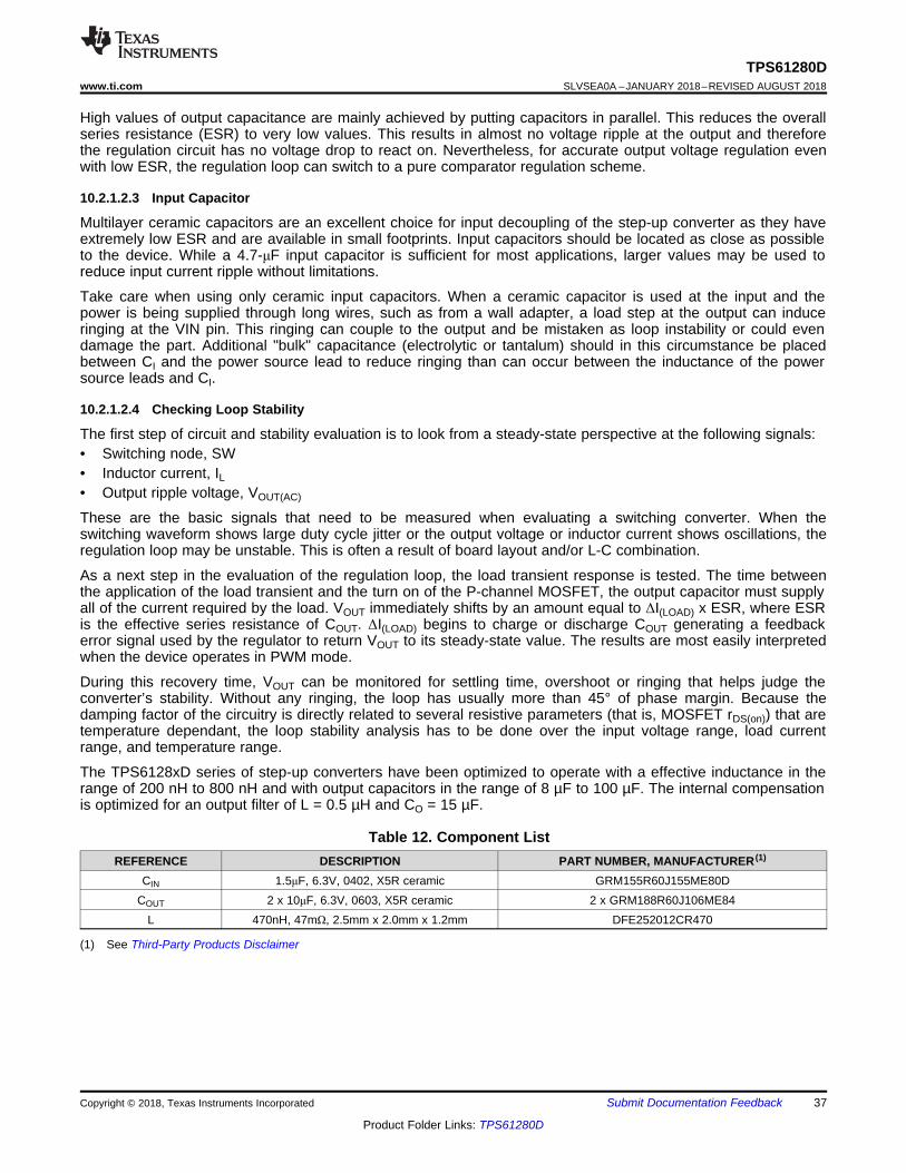
37
TPS61280Dwww.ti.com SLVSEA0A –JANUARY 2018–REVISED AUGUST 2018
Product Folder Links: TPS61280D
Submit Documentation FeedbackCopyright © 2018, Texas Instruments Incorporated
(1) See Third-Party Products Disclaimer
High values of output capacitance are mainly achieved by putting capacitors in parallel. This reduces the overallseries resistance (ESR) to very low values. This results in almost no voltage ripple at the output and thereforethe regulation circuit has no voltage drop to react on. Nevertheless, for accurate output voltage regulation evenwith low ESR, the regulation loop can switch to a pure comparator regulation scheme.
10.2.1.2.3 Input Capacitor
Multilayer ceramic capacitors are an excellent choice for input decoupling of the step-up converter as they haveextremely low ESR and are available in small footprints. Input capacitors should be located as close as possibleto the device. While a 4.7-μF input capacitor is sufficient for most applications, larger values may be used toreduce input current ripple without limitations.
Take care when using only ceramic input capacitors. When a ceramic capacitor is used at the input and thepower is being supplied through long wires, such as from a wall adapter, a load step at the output can induceringing at the VIN pin. This ringing can couple to the output and be mistaken as loop instability or could evendamage the part. Additional "bulk" capacitance (electrolytic or tantalum) should in this circumstance be placedbetween CI and the power source lead to reduce ringing than can occur between the inductance of the powersource leads and CI.
10.2.1.2.4 Checking Loop Stability
The first step of circuit and stability evaluation is to look from a steady-state perspective at the following signals:• Switching node, SW• Inductor current, IL• Output ripple voltage, VOUT(AC)
These are the basic signals that need to be measured when evaluating a switching converter. When theswitching waveform shows large duty cycle jitter or the output voltage or inductor current shows oscillations, theregulation loop may be unstable. This is often a result of board layout and/or L-C combination.
As a next step in the evaluation of the regulation loop, the load transient response is tested. The time betweenthe application of the load transient and the turn on of the P-channel MOSFET, the output capacitor must supplyall of the current required by the load. VOUT immediately shifts by an amount equal to ΔI(LOAD) x ESR, where ESRis the effective series resistance of COUT. ΔI(LOAD) begins to charge or discharge COUT generating a feedbackerror signal used by the regulator to return VOUT to its steady-state value. The results are most easily interpretedwhen the device operates in PWM mode.
During this recovery time, VOUT can be monitored for settling time, overshoot or ringing that helps judge theconverter’s stability. Without any ringing, the loop has usually more than 45° of phase margin. Because thedamping factor of the circuitry is directly related to several resistive parameters (that is, MOSFET rDS(on)) that aretemperature dependant, the loop stability analysis has to be done over the input voltage range, load currentrange, and temperature range.
The TPS6128xD series of step-up converters have been optimized to operate with a effective inductance in therange of 200 nH to 800 nH and with output capacitors in the range of 8 µF to 100 µF. The internal compensationis optimized for an output filter of L = 0.5 µH and CO = 15 µF.
Table 12. Component ListREFERENCE DESCRIPTION PART NUMBER, MANUFACTURER (1)
CIN 1.5μF, 6.3V, 0402, X5R ceramic GRM155R60J155ME80DCOUT 2 x 10μF, 6.3V, 0603, X5R ceramic 2 x GRM188R60J106ME84
L 470nH, 47mΩ, 2.5mm x 2.0mm x 1.2mm DFE252012CR470
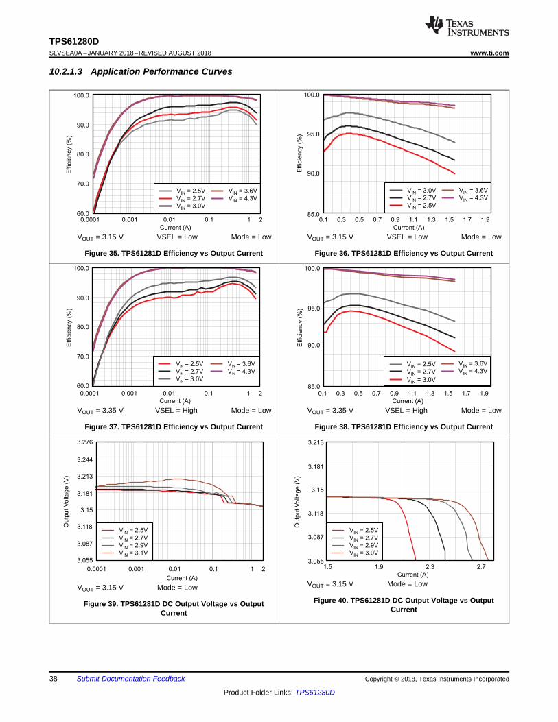
3.055
3.087
3.118
3.15
3.181
3.213
3.244
3.276
0.0001 0.001 0.01 0.1 1 2
Current (A)
Ou
tpu
t V
olta
ge
(V
)
V = 2.5VIN
VIN = 2.7V
VIN = 2.9V
VIN = 3.1V
3.055
3.087
3.118
3.15
3.181
3.213
1.5 1.9 2.3 2.7
Current (A)
Ou
tpu
t V
olta
ge
(V
)
V = 2.5VIN
VIN = 2.7V
VIN = 2.9V
VIN = 3.0V
60.0
70.0
80.0
90.0
100.0
0.0001 0.001 0.01 0.1 1 2
Current (A)
Effic
ien
cy (
%)
V = 2.5VIN
VIN = 2.7V
VIN = 3.0V
VIN = 3.6V
VIN = 4.3V
85.0
90.0
95.0
100.0
0.1 0.3 0.5 0.7 0.9 1.1 1.3 1.5 1.7 1.9
Current (A)
Effic
ien
cy (
%)
V = 3.0VIN
VIN = 2.7V
VIN = 2.5V VIN = 3.6V
VIN = 4.3V
60.0
70.0
80.0
90.0
100.0
0.0001 0.001 0.01 0.1 1 2
Current (A)
Effic
iency (
%)
V = 2.5VIN
VIN = 2.7V
VIN = 3.0V
VIN = 3.6V
VIN = 4.3V
85.0
90.0
95.0
100.0
0.1 0.3 0.5 0.7 0.9 1.1 1.3 1.5 1.7 1.9
Current (A)
Effic
ien
cy (
%)
V = 2.5VIN
VIN = 2.7VVIN = 3.0V VIN = 3.6V
VIN = 4.3V
38
TPS61280DSLVSEA0A –JANUARY 2018–REVISED AUGUST 2018 www.ti.com
Product Folder Links: TPS61280D
Submit Documentation Feedback Copyright © 2018, Texas Instruments Incorporated
10.2.1.3 Application Performance Curves
VOUT = 3.15 V VSEL = Low Mode = Low
Figure 35. TPS61281D Efficiency vs Output Current
VOUT = 3.15 V VSEL = Low Mode = Low
Figure 36. TPS61281D Efficiency vs Output Current
VOUT = 3.35 V VSEL = High Mode = Low
Figure 37. TPS61281D Efficiency vs Output Current
VOUT = 3.35 V VSEL = High Mode = Low
Figure 38. TPS61281D Efficiency vs Output Current
VOUT = 3.15 V Mode = Low
Figure 39. TPS61281D DC Output Voltage vs OutputCurrent
VOUT = 3.15 V Mode = Low
Figure 40. TPS61281D DC Output Voltage vs OutputCurrent
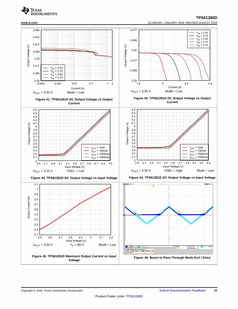
2.1
2.2
2.3
2.4
2.5
2.6
2.7
2.8
2.9
3
3.1
2.5 2.6 2.7 2.8 2.9 3 3.1 3.2
Input Voltage (V)
Ou
tpu
t C
urr
en
t (A
)
3
3.1
3.2
3.3
3.4
3.5
3.6
3.7
3.8
3.9
4
4.1
4.2
4.3
4.4
4.5
2.5 2.7 2.9 3.1 3.3 3.5 3.7 3.9 4.1 4.3 4.5
Input Voltage (V)
Ou
tpu
t V
olta
ge
(V
)
I = 1mAOUT
I = 100mAOUT
I = 1000mAOUT
I = 1500mAOUT
3
3.1
3.2
3.3
3.4
3.5
3.6
3.7
3.8
3.9
4
4.1
4.2
4.3
4.4
4.5
2.5 2.7 2.9 3.1 3.3 3.5 3.7 3.9 4.1 4.3 4.5
Input Voltage (V)
Outp
ut V
oltage (
V)
I = 1mAOUT
IOUT = 100mA
IOUT = 1000mA
IOUT = 1500mA
3.25
3.284
3.317
3.35
3.384
3.417
3.451
3.484
0.0001 0.001 0.01 0.1 1 2
Current (A)
Ou
tpu
t V
olta
ge
(V
)
V = 2.5VIN
VIN = 2.7V
VIN = 2.9V
VIN = 3.1V3.25
3.284
3.317
3.35
3.384
3.417
1.6 2 2.4 2.8
Current (A)
Ou
tpu
t V
olta
ge
(V
)
V = 2.5VIN
VIN = 2.7V
VIN = 2.9V
VIN = 3.1V
VIN = 3.2V
39
TPS61280Dwww.ti.com SLVSEA0A –JANUARY 2018–REVISED AUGUST 2018
Product Folder Links: TPS61280D
Submit Documentation FeedbackCopyright © 2018, Texas Instruments Incorporated
VOUT = 3.35 V Mode = Low
Figure 41. TPS61281D DC Output Voltage vs OutputCurrent
VOUT = 3.35 V Mode = Low
Figure 42. TPS61281D DC Output Voltage vs OutputCurrent
VOUT = 3.15 V VSEL = Low
Figure 43. TPS61281D DC Output Voltage vs Input Voltage
VOUT = 3.35 V VSEL = High Mode = Low
Figure 44. TPS61281D DC Output Voltage vs Input Voltage
VOUT = 3.35 V TA = 85°C Mode = Low
Figure 45. TPS61281D Maximum Output Current vs InputVoltage
Figure 46. Boost to Pass-Through Mode Exit / Entry
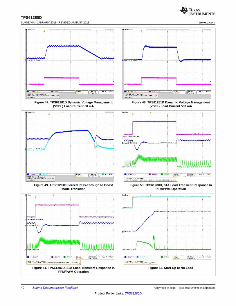
40
TPS61280DSLVSEA0A –JANUARY 2018–REVISED AUGUST 2018 www.ti.com
Product Folder Links: TPS61280D
Submit Documentation Feedback Copyright © 2018, Texas Instruments Incorporated
Figure 47. TPS61281D Dynamic Voltage Management(VSEL) Load Current 50 mA
Figure 48. TPS61281D Dynamic Voltage Management(VSEL) Load Current 500 mA
Figure 49. TPS61281D Forced Pass-Through to BoostMode Transition
Figure 50. TPS61280D, 81A Load Transient Response InPFM/PWM Operation
Figure 51. TPS61280D, 81A Load Transient Response InPFM/PWM Operation
Figure 52. Start-Up at No Load
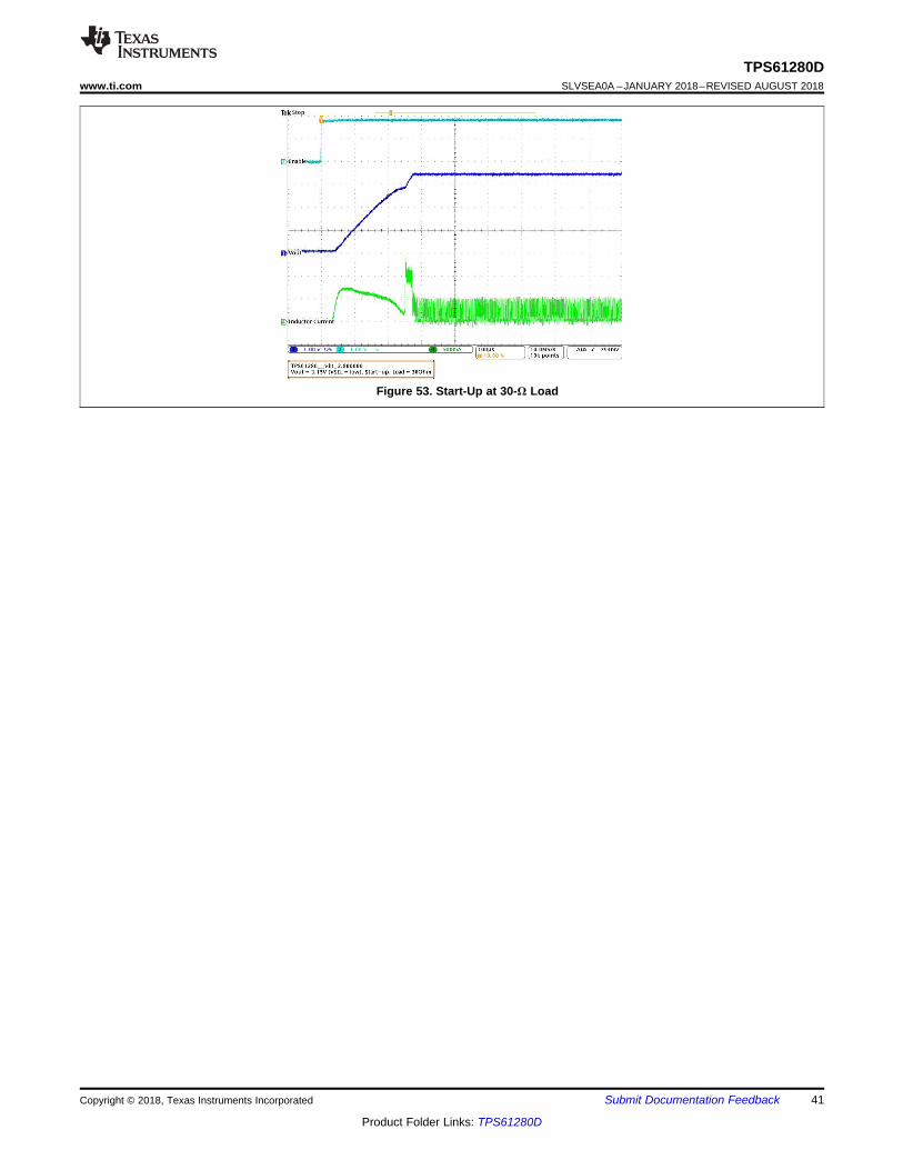
41
TPS61280Dwww.ti.com SLVSEA0A –JANUARY 2018–REVISED AUGUST 2018
Product Folder Links: TPS61280D
Submit Documentation FeedbackCopyright © 2018, Texas Instruments Incorporated
Figure 53. Start-Up at 30-Ω Load
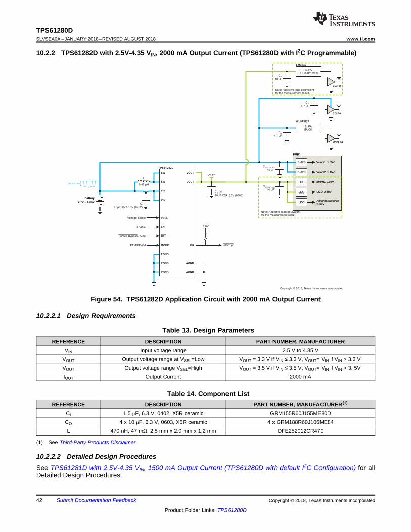
VBAT’
Battery
2.7V .. 4.35V
PMIC
eMMC, 2.95V
LCD, 2.80V
Antenna switches2.60V
C
10 FDECOUPLING
µ
Vcore1, 1.05V
Vcore2, 1.15V
C
10 FDECOUPLING
µ
WIFI PA
WL8PM27
C
4.7 FIN
µ
SMPS
SMPS
SuPABUCK
Battery
PMIC
eMMC, 2.95V
LCD, 2.80V
Antenna switches2.60V
Vcore1, 1.05V
Vcore2, 1.15V
WIFI PA
SMPS
SMPS
SuPABUCK
LDOLDO
LDOLDO
LDOLDO
2G PA
C
4.7 µFIN
3G PA
LM3242
C
10 µFIN
3G PA
SuPABUCK/BYPASS
200 to 600mV
2.7V
C
1.5µF X5R 6.3V (0402)I
C (x4)
10µF X5R 6.3V (0603)O
L
0.47 μH
TPS61282D
SW
SW
VIN
VIN
VSEL
BYP
MODE
PGND
PGND
PGND
EN
VOUT
VOUT
PG
AGND
AGND
Enable 1.8V
Interrupt
Forced Bypass / Auto
Voltage Select
PFM/FPWM
Note: Resistive load equivalentfor the measurement result.
Note: Resistive load equivalentfor the measurement result.
Copyright © 2016, Texas Instruments Incorporated
42
TPS61280DSLVSEA0A –JANUARY 2018–REVISED AUGUST 2018 www.ti.com
Product Folder Links: TPS61280D
Submit Documentation Feedback Copyright © 2018, Texas Instruments Incorporated
10.2.2 TPS61282D with 2.5V-4.35 VIN, 2000 mA Output Current (TPS61280D with I2C Programmable)
Figure 54. TPS61282D Application Circuit with 2000 mA Output Current
10.2.2.1 Design Requirements
Table 13. Design ParametersREFERENCE DESCRIPTION PART NUMBER, MANUFACTURER
VIN Input voltage range 2.5 V to 4.35 VVOUT Output voltage range at VSEL=Low VOUT = 3.3 V if VIN ≤ 3.3 V, VOUT= VIN if VIN > 3.3 VVOUT Output voltage range VSEL=High VOUT = 3.5 V if VIN ≤ 3.5 V, VOUT= VIN if VIN > 3. 5VIOUT Output Current 2000 mA
(1) See Third-Party Products Disclaimer
Table 14. Component ListREFERENCE DESCRIPTION PART NUMBER, MANUFACTURER (1)
CI 1.5 μF, 6.3 V, 0402, X5R ceramic GRM155R60J155ME80DCO 4 x 10 μF, 6.3 V, 0603, X5R ceramic 4 x GRM188R60J106ME84L 470 nH, 47 mΩ, 2.5 mm x 2.0 mm x 1.2 mm DFE252012CR470
10.2.2.2 Detailed Design ProceduresSee TPS61281D with 2.5V-4.35 VIN, 1500 mA Output Current (TPS61280D with default I2C Configuration) for allDetailed Design Procedures.
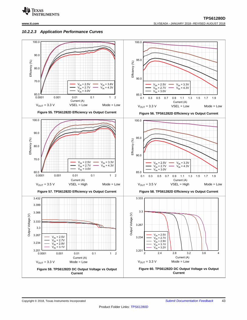
3.201
3.234
3.267
3.3
3.333
3.366
3.399
3.432
0.0001 0.001 0.01 0.1 1 2
Current (A)
Ou
tpu
t V
olta
ge
(V
)
V = 2.5VIN
VIN = 2.7V
VIN = 2.9V
VIN = 3.1V
3.201
3.234
3.267
3.3
3.333
2 2.4 2.8 3.2 3.6 4
Current (A)
Ou
tpu
t V
olta
ge
(V
)
V = 2.5VIN
VIN = 2.7V
VIN = 2.9V
VIN = 3.1V
VIN = 3.2V
60.0
70.0
80.0
90.0
100.0
0.0001 0.001 0.01 0.1 1 2
Current (A)
Effic
ien
cy (
%)
V = 2.5VIN
VIN = 2.7V
VIN = 3.0V
VIN = 3.3V
VIN = 4.3V
85.0
90.0
95.0
100.0
0.1 0.3 0.5 0.7 0.9 1.1 1.3 1.5 1.7 1.9
Current (A)
Effic
iency (
%)
V = 2.5VIN
VIN = 2.7V
VIN = 3.0V
VIN = 3.3V
VIN = 4.3V
85.0
90.0
95.0
100.0
0.1 0.3 0.5 0.7 0.9 1.1 1.3 1.5 1.7 1.9
Current (A)
Effic
ien
cy (
%)
V = 2.5VIN
VIN = 2.7V
VIN = 3.0V
VIN = 3.3V
VIN = 4.3V
60.0
70.0
80.0
90.0
100.0
0.0001 0.001 0.01 0.1 1 2
Current (A)
Effic
ien
cy (
%)
V = 2.5VIN
VIN = 2.7V
VIN = 3.0V
VIN = 3.6V
VIN = 4.3V
43
TPS61280Dwww.ti.com SLVSEA0A –JANUARY 2018–REVISED AUGUST 2018
Product Folder Links: TPS61280D
Submit Documentation FeedbackCopyright © 2018, Texas Instruments Incorporated
10.2.2.3 Application Performance Curves
VOUT = 3.3 V VSEL = Low Mode = Low
Figure 55. TPS61282D Efficiency vs Output Current
VOUT = 3.3 V VSEL = Low Mode = Low
Figure 56. TPS61282D Efficiency vs Output Current
VOUT = 3.5 V VSEL = High Mode = Low
Figure 57. TPS61282D Efficiency vs Output Current
VOUT = 3.5 V VSEL = High Mode = Low
Figure 58. TPS61282D Efficiency vs Output Current
VOUT = 3.3 V Mode = Low
Figure 59. TPS61282D DC Output Voltage vs OutputCurrent
VOUT = 3.3 V Mode = Low
Figure 60. TPS61282D DC Output Voltage vs OutputCurrent
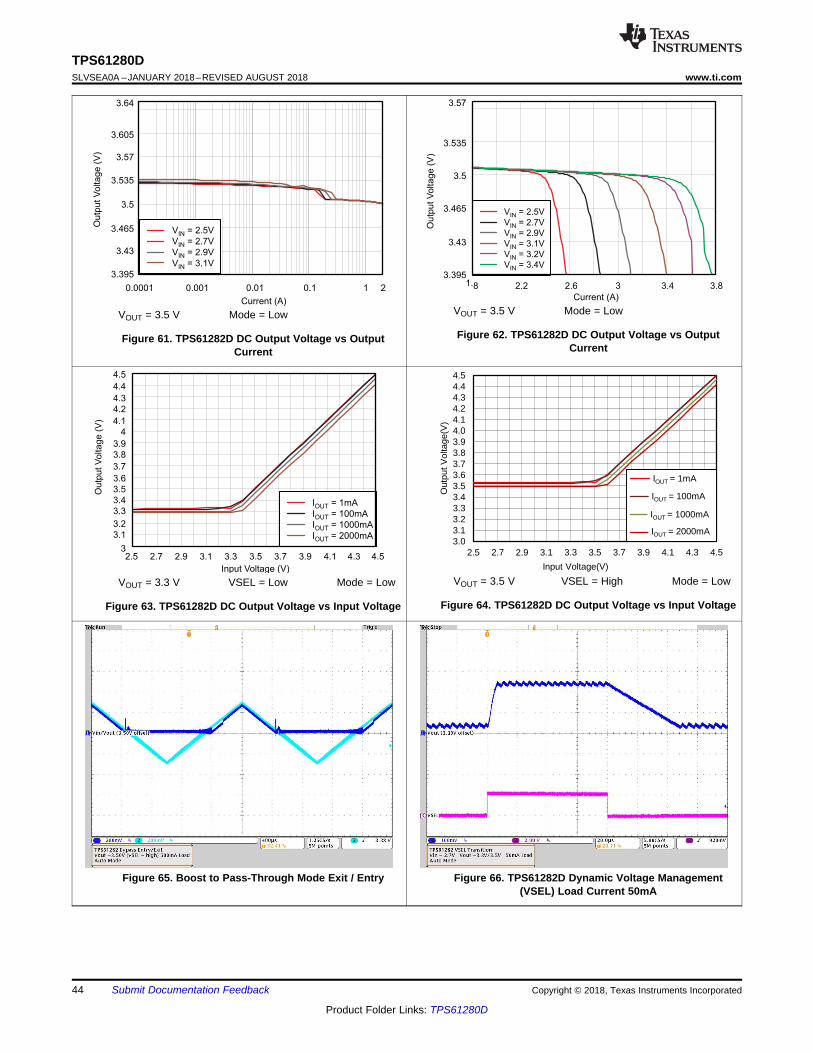
3
3.1
3.2
3.3
3.4
3.5
3.6
3.7
3.8
3.9
4
4.1
4.2
4.3
4.4
4.5
2.5 2.7 2.9 3.1 3.3 3.5 3.7 3.9 4.1 4.3 4.5
Input Voltage (V)
Ou
tpu
t V
olta
ge
(V
)
I = 1mAOUT
IOUT = 100mA
IOUT = 1000mA
IOUT = 2000mA3.0 3.1 3.2 3.3 3.4 3.5 3.6 3.7 3.8 3.9 4.0 4.1 4.2 4.3 4.4 4.5
2.5 2.7 2.9 3.1 3.3 3.5 3.7 3.9 4.1 4.3 4.5
Out
put V
olta
ge(V
)
Input Voltage(V)
Iout=1mA
Iout=100mA
Iout=1000mA
Iout=2000mA
C013
IOUT = 1mA
IOUT = 100mA
IOUT = 1000mA
IOUT = 2000mA
3.395
3.43
3.465
3.5
3.535
3.57
3.605
3.64
0.0001 0.001 0.01 0.1 1 2
Current (A)
Outp
ut V
oltage (
V)
V = 2.5VIN
VIN = 2.7V
VIN = 2.9V
VIN = 3.1V
3.395
3.43
3.465
3.5
3.535
3.57
1.8 2.2 2.6 3 3.4 3.8
Current (A)
Outp
ut V
oltage (
V)
V = 2.5VIN
VIN = 2.7V
VIN = 2.9V
VIN = 3.1V
VIN = 3.2V
VIN = 3.4V
44
TPS61280DSLVSEA0A –JANUARY 2018–REVISED AUGUST 2018 www.ti.com
Product Folder Links: TPS61280D
Submit Documentation Feedback Copyright © 2018, Texas Instruments Incorporated
VOUT = 3.5 V Mode = Low
Figure 61. TPS61282D DC Output Voltage vs OutputCurrent
VOUT = 3.5 V Mode = Low
Figure 62. TPS61282D DC Output Voltage vs OutputCurrent
VOUT = 3.3 V VSEL = Low Mode = Low
Figure 63. TPS61282D DC Output Voltage vs Input Voltage
VOUT = 3.5 V VSEL = High Mode = Low
Figure 64. TPS61282D DC Output Voltage vs Input Voltage
Figure 65. Boost to Pass-Through Mode Exit / Entry Figure 66. TPS61282D Dynamic Voltage Management(VSEL) Load Current 50mA

45
TPS61280Dwww.ti.com SLVSEA0A –JANUARY 2018–REVISED AUGUST 2018
Product Folder Links: TPS61280D
Submit Documentation FeedbackCopyright © 2018, Texas Instruments Incorporated
Figure 67. TPS61282D Dynamic Voltage Management(VSEL) Load Current 500mA
Figure 68. TPS61282D Line Transient
Figure 69. TPS61282D Load Transient Response In PWMOperation
Figure 70. TPS61282D Load Transient Response InPFM/PWM Operation
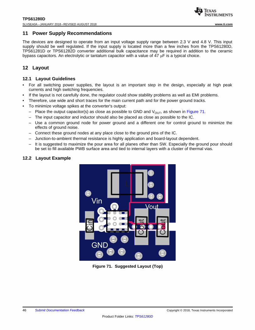
Cout
Cout
L
Cin
VinVout
GND
46
TPS61280DSLVSEA0A –JANUARY 2018–REVISED AUGUST 2018 www.ti.com
Product Folder Links: TPS61280D
Submit Documentation Feedback Copyright © 2018, Texas Instruments Incorporated
11 Power Supply RecommendationsThe devices are designed to operate from an input voltage supply range between 2.3 V and 4.8 V. This inputsupply should be well regulated. If the input supply is located more than a few inches from the TPS61280D,TPS61281D or TPS61282D converter additional bulk capacitance may be required in addition to the ceramicbypass capacitors. An electrolytic or tantalum capacitor with a value of 47 μF is a typical choice.
12 Layout
12.1 Layout Guidelines• For all switching power supplies, the layout is an important step in the design, especially at high peak
currents and high switching frequencies.• If the layout is not carefully done, the regulator could show stability problems as well as EMI problems.• Therefore, use wide and short traces for the main current path and for the power ground tracks.• To minimize voltage spikes at the converter's output:
– Place the output capacitor(s) as close as possible to GND and VOUT, as shown in Figure 71.– The input capacitor and inductor should also be placed as close as possible to the IC.– Use a common ground node for power ground and a different one for control ground to minimize the
effects of ground noise.– Connect these ground nodes at any place close to the ground pins of the IC.– Junction-to-ambient thermal resistance is highly application and board-layout dependent.– It is suggested to maximize the pour area for all planes other than SW. Especially the ground pour should
be set to fill available PWB surface area and tied to internal layers with a cluster of thermal vias.
12.2 Layout Example
Figure 71. Suggested Layout (Top)
47
TPS61280Dwww.ti.com SLVSEA0A –JANUARY 2018–REVISED AUGUST 2018
Product Folder Links: TPS61280D
Submit Documentation FeedbackCopyright © 2018, Texas Instruments Incorporated
12.3 Thermal InformationImplementation of integrated circuits in low-profile and fine-pitch surface-mount packages typically requiresspecial attention to power dissipation. Many system-dependent issues such as thermal coupling, airflow, addedheat sinks and convection surfaces, and the presence of other heat-generating components affect the power-dissipation limits of a given component.
Three basic approaches for enhancing thermal performance are listed below:• Improving the power dissipation capability of the PCB design• Improving the thermal coupling of the component to the PCB• Introducing airflow in the system
As power demand in portable designs is more and more important, designers must figure the best trade-offbetween efficiency, power dissipation and solution size. Due to integration and miniaturization, junctiontemperature can increase significantly which could lead to bad application behaviors (that is, premature thermalshutdown or worst case reduce device reliability).
Junction-to-ambient thermal resistance is highly application and board-layout dependent. In applications wherehigh maximum power dissipation exists, special care must be paid to thermal dissipation issues in board design.The device operating junction temperature (TJ) should be kept below 125°C.

48
TPS61280DSLVSEA0A –JANUARY 2018–REVISED AUGUST 2018 www.ti.com
Product Folder Links: TPS61280D
Submit Documentation Feedback Copyright © 2018, Texas Instruments Incorporated
13 Device and Documentation Support
13.1 Device Support
13.1.1 Third-Party Products DisclaimerTI'S PUBLICATION OF INFORMATION REGARDING THIRD-PARTY PRODUCTS OR SERVICES DOES NOTCONSTITUTE AN ENDORSEMENT REGARDING THE SUITABILITY OF SUCH PRODUCTS OR SERVICESOR A WARRANTY, REPRESENTATION OR ENDORSEMENT OF SUCH PRODUCTS OR SERVICES, EITHERALONE OR IN COMBINATION WITH ANY TI PRODUCT OR SERVICE.
13.2 Receiving Notification of Documentation UpdatesTo receive notification of documentation updates, navigate to the device product folder on ti.com. In the upperright corner, click on Alert me to register and receive a weekly digest of any product information that haschanged. For change details, review the revision history included in any revised document.
13.3 Community ResourcesThe following links connect to TI community resources. Linked contents are provided "AS IS" by the respectivecontributors. They do not constitute TI specifications and do not necessarily reflect TI's views; see TI's Terms ofUse.
TI E2E™ Online Community TI's Engineer-to-Engineer (E2E) Community. Created to foster collaborationamong engineers. At e2e.ti.com, you can ask questions, share knowledge, explore ideas and helpsolve problems with fellow engineers.
Design Support TI's Design Support Quickly find helpful E2E forums along with design support tools andcontact information for technical support.
13.4 TrademarksE2E is a trademark of Texas Instruments.I2C is a trademark of NXP Semiconductors.All other trademarks are the property of their respective owners.
13.5 Electrostatic Discharge CautionThis integrated circuit can be damaged by ESD. Texas Instruments recommends that all integrated circuits be handled withappropriate precautions. Failure to observe proper handling and installation procedures can cause damage.
ESD damage can range from subtle performance degradation to complete device failure. Precision integrated circuits may be moresusceptible to damage because very small parametric changes could cause the device not to meet its published specifications.
13.6 GlossarySLYZ022 — TI Glossary.
This glossary lists and explains terms, acronyms, and definitions.
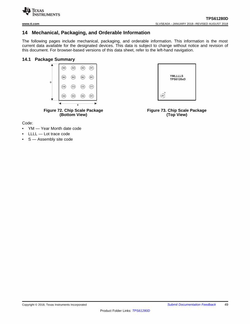
A1
C1
A2
D
E
C2
A3
C3
A4
C4
D1D2D3D4
B1B2B3B4
A1
YMLLLLS
TPS6128xD
49
TPS61280Dwww.ti.com SLVSEA0A –JANUARY 2018–REVISED AUGUST 2018
Product Folder Links: TPS61280D
Submit Documentation FeedbackCopyright © 2018, Texas Instruments Incorporated
14 Mechanical, Packaging, and Orderable InformationThe following pages include mechanical, packaging, and orderable information. This information is the mostcurrent data available for the designated devices. This data is subject to change without notice and revision ofthis document. For browser-based versions of this data sheet, refer to the left-hand navigation.
14.1 Package Summary
Figure 72. Chip Scale Package(Bottom View)
Figure 73. Chip Scale Package(Top View)
Code:• YM — Year Month date code• LLLL — Lot trace code• S — Assembly site code
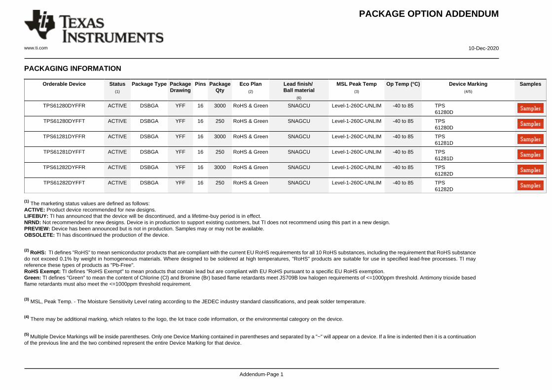
PACKAGE OPTION ADDENDUM
www.ti.com 10-Dec-2020
Addendum-Page 1
PACKAGING INFORMATION
Orderable Device Status(1)
Package Type PackageDrawing
Pins PackageQty
Eco Plan(2)
Lead finish/Ball material
(6)
MSL Peak Temp(3)
Op Temp (°C) Device Marking(4/5)
Samples
TPS61280DYFFR ACTIVE DSBGA YFF 16 3000 RoHS & Green SNAGCU Level-1-260C-UNLIM -40 to 85 TPS61280D
TPS61280DYFFT ACTIVE DSBGA YFF 16 250 RoHS & Green SNAGCU Level-1-260C-UNLIM -40 to 85 TPS61280D
TPS61281DYFFR ACTIVE DSBGA YFF 16 3000 RoHS & Green SNAGCU Level-1-260C-UNLIM -40 to 85 TPS61281D
TPS61281DYFFT ACTIVE DSBGA YFF 16 250 RoHS & Green SNAGCU Level-1-260C-UNLIM -40 to 85 TPS61281D
TPS61282DYFFR ACTIVE DSBGA YFF 16 3000 RoHS & Green SNAGCU Level-1-260C-UNLIM -40 to 85 TPS61282D
TPS61282DYFFT ACTIVE DSBGA YFF 16 250 RoHS & Green SNAGCU Level-1-260C-UNLIM -40 to 85 TPS61282D
(1) The marketing status values are defined as follows:ACTIVE: Product device recommended for new designs.LIFEBUY: TI has announced that the device will be discontinued, and a lifetime-buy period is in effect.NRND: Not recommended for new designs. Device is in production to support existing customers, but TI does not recommend using this part in a new design.PREVIEW: Device has been announced but is not in production. Samples may or may not be available.OBSOLETE: TI has discontinued the production of the device.
(2) RoHS: TI defines "RoHS" to mean semiconductor products that are compliant with the current EU RoHS requirements for all 10 RoHS substances, including the requirement that RoHS substancedo not exceed 0.1% by weight in homogeneous materials. Where designed to be soldered at high temperatures, "RoHS" products are suitable for use in specified lead-free processes. TI mayreference these types of products as "Pb-Free".RoHS Exempt: TI defines "RoHS Exempt" to mean products that contain lead but are compliant with EU RoHS pursuant to a specific EU RoHS exemption.Green: TI defines "Green" to mean the content of Chlorine (Cl) and Bromine (Br) based flame retardants meet JS709B low halogen requirements of <=1000ppm threshold. Antimony trioxide basedflame retardants must also meet the <=1000ppm threshold requirement.
(3) MSL, Peak Temp. - The Moisture Sensitivity Level rating according to the JEDEC industry standard classifications, and peak solder temperature.
(4) There may be additional marking, which relates to the logo, the lot trace code information, or the environmental category on the device.
(5) Multiple Device Markings will be inside parentheses. Only one Device Marking contained in parentheses and separated by a "~" will appear on a device. If a line is indented then it is a continuationof the previous line and the two combined represent the entire Device Marking for that device.
PACKAGE OPTION ADDENDUM
www.ti.com 10-Dec-2020
Addendum-Page 2
(6) Lead finish/Ball material - Orderable Devices may have multiple material finish options. Finish options are separated by a vertical ruled line. Lead finish/Ball material values may wrap to twolines if the finish value exceeds the maximum column width.
Important Information and Disclaimer:The information provided on this page represents TI's knowledge and belief as of the date that it is provided. TI bases its knowledge and belief on informationprovided by third parties, and makes no representation or warranty as to the accuracy of such information. Efforts are underway to better integrate information from third parties. TI has taken andcontinues to take reasonable steps to provide representative and accurate information but may not have conducted destructive testing or chemical analysis on incoming materials and chemicals.TI and TI suppliers consider certain information to be proprietary, and thus CAS numbers and other limited information may not be available for release.
In no event shall TI's liability arising out of such information exceed the total purchase price of the TI part(s) at issue in this document sold by TI to Customer on an annual basis.
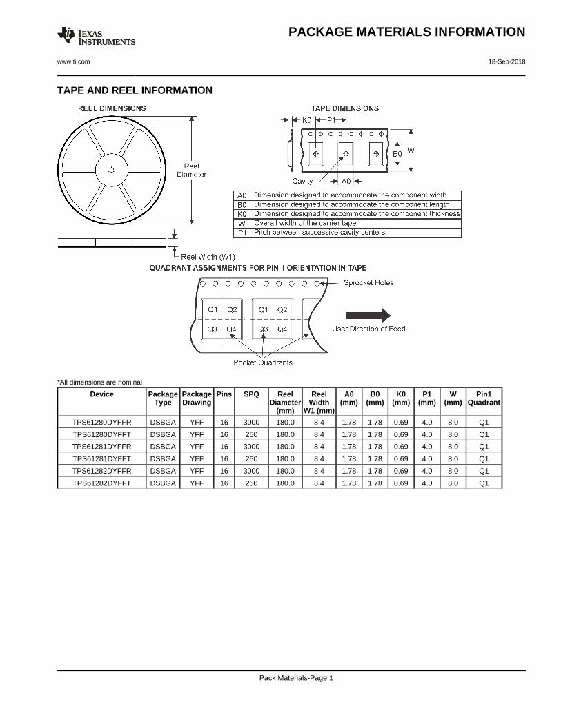
TAPE AND REEL INFORMATION
*All dimensions are nominal
Device PackageType
PackageDrawing
Pins SPQ ReelDiameter
(mm)
ReelWidth
W1 (mm)
A0(mm)
B0(mm)
K0(mm)
P1(mm)
W(mm)
Pin1Quadrant
TPS61280DYFFR DSBGA YFF 16 3000 180.0 8.4 1.78 1.78 0.69 4.0 8.0 Q1
TPS61280DYFFT DSBGA YFF 16 250 180.0 8.4 1.78 1.78 0.69 4.0 8.0 Q1
TPS61281DYFFR DSBGA YFF 16 3000 180.0 8.4 1.78 1.78 0.69 4.0 8.0 Q1
TPS61281DYFFT DSBGA YFF 16 250 180.0 8.4 1.78 1.78 0.69 4.0 8.0 Q1
TPS61282DYFFR DSBGA YFF 16 3000 180.0 8.4 1.78 1.78 0.69 4.0 8.0 Q1
TPS61282DYFFT DSBGA YFF 16 250 180.0 8.4 1.78 1.78 0.69 4.0 8.0 Q1
PACKAGE MATERIALS INFORMATION
www.ti.com 18-Sep-2018
Pack Materials-Page 1
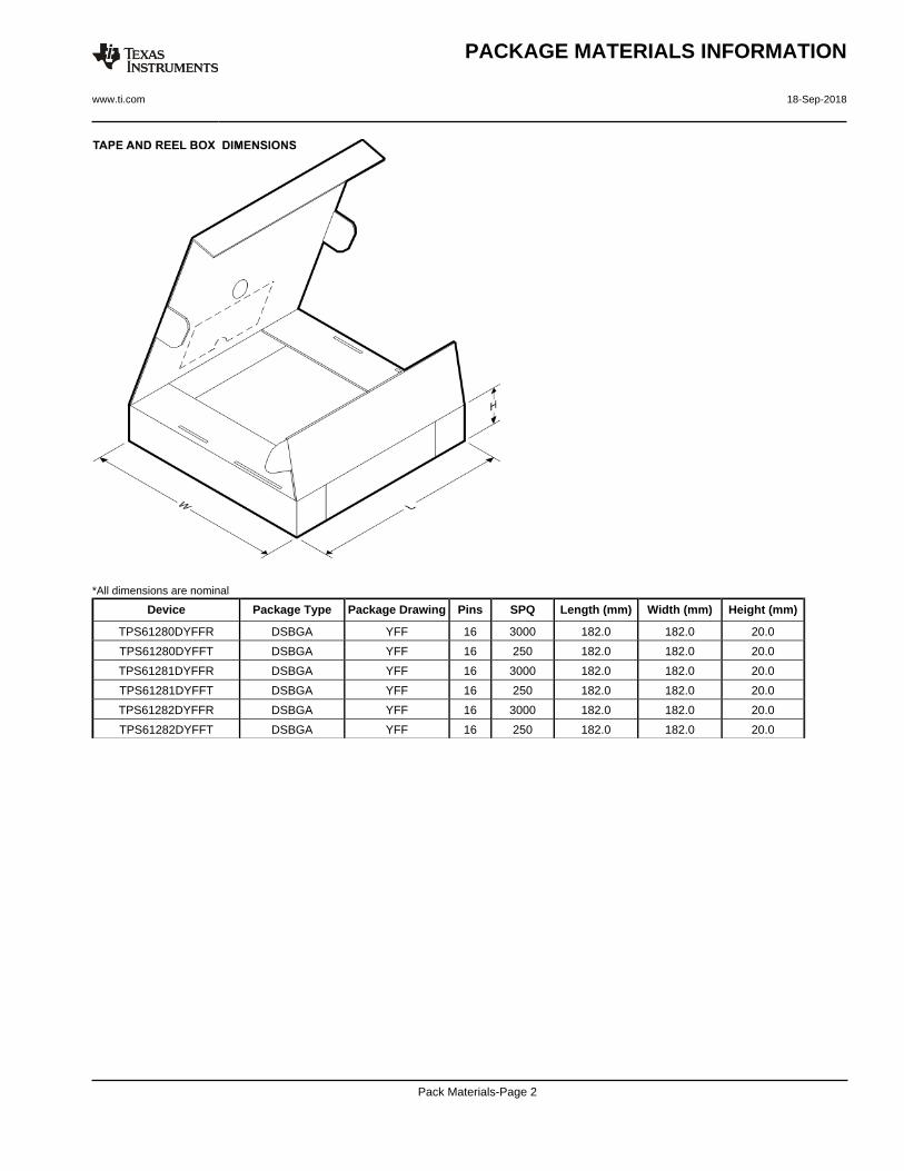
*All dimensions are nominal
Device Package Type Package Drawing Pins SPQ Length (mm) Width (mm) Height (mm)
TPS61280DYFFR DSBGA YFF 16 3000 182.0 182.0 20.0
TPS61280DYFFT DSBGA YFF 16 250 182.0 182.0 20.0
TPS61281DYFFR DSBGA YFF 16 3000 182.0 182.0 20.0
TPS61281DYFFT DSBGA YFF 16 250 182.0 182.0 20.0
TPS61282DYFFR DSBGA YFF 16 3000 182.0 182.0 20.0
TPS61282DYFFT DSBGA YFF 16 250 182.0 182.0 20.0
PACKAGE MATERIALS INFORMATION
www.ti.com 18-Sep-2018
Pack Materials-Page 2
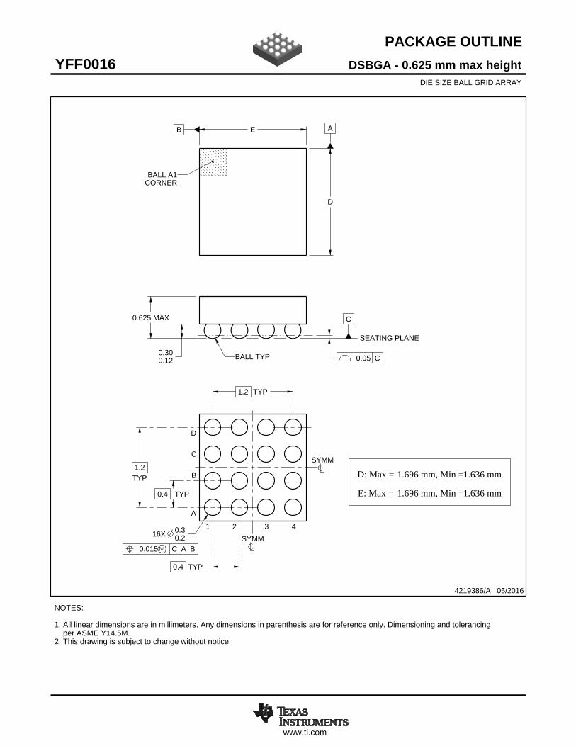
www.ti.com
PACKAGE OUTLINE
C0.625 MAX
0.300.12
1.2TYP
1.2 TYP
0.4 TYP
0.4 TYP
16X 0.30.2
B E A
D
DSBGA - 0.625 mm max heightYFF0016DIE SIZE BALL GRID ARRAY
4219386/A 05/2016
NOTES: 1. All linear dimensions are in millimeters. Any dimensions in parenthesis are for reference only. Dimensioning and tolerancing per ASME Y14.5M.2. This drawing is subject to change without notice.
BALL A1CORNER
SEATING PLANE
BALL TYP 0.05 C
B
1 2 3
0.015 C A B
SYMM
SYMM
A
C
D
4
SCALE 8.000
D: Max =
E: Max =
1.696 mm, Min =
1.696 mm, Min =
1.636 mm
1.636 mm

www.ti.com
EXAMPLE BOARD LAYOUT
16X ( 0.23)
(0.4) TYP
(0.4) TYP
( 0.23)METAL
0.05 MAX
SOLDER MASKOPENING
METAL UNDERSOLDER MASK
( 0.23)SOLDER MASKOPENING
0.05 MIN
DSBGA - 0.625 mm max heightYFF0016DIE SIZE BALL GRID ARRAY
4219386/A 05/2016
NOTES: (continued) 3. Final dimensions may vary due to manufacturing tolerance considerations and also routing constraints. For more information, see Texas Instruments literature number SNVA009 (www.ti.com/lit/snva009).
SYMM
SYMM
LAND PATTERN EXAMPLESCALE:30X
C
1 2 3
A
B
D
4
NON-SOLDER MASKDEFINED
(PREFERRED)
SOLDER MASK DETAILSNOT TO SCALE
SOLDER MASKDEFINED
www.ti.com
EXAMPLE STENCIL DESIGN
(0.4) TYP
(0.4) TYP
16X ( 0.25) (R0.05) TYP
METALTYP
DSBGA - 0.625 mm max heightYFF0016DIE SIZE BALL GRID ARRAY
4219386/A 05/2016
NOTES: (continued) 4. Laser cutting apertures with trapezoidal walls and rounded corners may offer better paste release.
SYMM
SYMM
C
1 2 3A
B
D
SOLDER PASTE EXAMPLEBASED ON 0.1 mm THICK STENCIL
SCALE:30X
4

IMPORTANT NOTICE AND DISCLAIMER
TI PROVIDES TECHNICAL AND RELIABILITY DATA (INCLUDING DATASHEETS), DESIGN RESOURCES (INCLUDING REFERENCE DESIGNS), APPLICATION OR OTHER DESIGN ADVICE, WEB TOOLS, SAFETY INFORMATION, AND OTHER RESOURCES “AS IS” AND WITH ALL FAULTS, AND DISCLAIMS ALL WARRANTIES, EXPRESS AND IMPLIED, INCLUDING WITHOUT LIMITATION ANY IMPLIED WARRANTIES OF MERCHANTABILITY, FITNESS FOR A PARTICULAR PURPOSE OR NON-INFRINGEMENT OF THIRD PARTY INTELLECTUAL PROPERTY RIGHTS.These resources are intended for skilled developers designing with TI products. You are solely responsible for (1) selecting the appropriate TI products for your application, (2) designing, validating and testing your application, and (3) ensuring your application meets applicable standards, and any other safety, security, or other requirements. These resources are subject to change without notice. TI grants you permission to use these resources only for development of an application that uses the TI products described in the resource. Other reproduction and display of these resources is prohibited. No license is granted to any other TI intellectual property right or to any third party intellectual property right. TI disclaims responsibility for, and you will fully indemnify TI and its representatives against, any claims, damages, costs, losses, and liabilities arising out of your use of these resources.TI’s products are provided subject to TI’s Terms of Sale (www.ti.com/legal/termsofsale.html) or other applicable terms available either on ti.com or provided in conjunction with such TI products. TI’s provision of these resources does not expand or otherwise alter TI’s applicable warranties or warranty disclaimers for TI products.
Mailing Address: Texas Instruments, Post Office Box 655303, Dallas, Texas 75265Copyright © 2020, Texas Instruments Incorporated