Embed Size (px)
Citation preview
IOUT (mA)
Effi
cien
cy
0.001 0.01 0.1 1 10 100 100050%
55%
60%
65%
70%
75%
80%
85%
90%
95%
100%
D006
VIN = 3.6 VVIN = 4.2 VVIN = 5.0 V
VIN
EN
VSEL1
VSEL2
VSEL3
SW
VOS
GND
L 2.2 PH
COUT
10 PFCIN
4.7 PF
VIN
2.0 V to 5.5 VLow Power MCU & RF
TPS62743VOUT
Copyright © 2016, Texas Instruments Incorporated
Product
Folder
Order
Now
Technical
Documents
Tools &
Software
Support &Community
An IMPORTANT NOTICE at the end of this data sheet addresses availability, warranty, changes, use in safety-critical applications,intellectual property matters and other important disclaimers. PRODUCTION DATA.
TPS62743, TPS627431SLVSCQ0A –JUNE 2015–REVISED MAY 2016
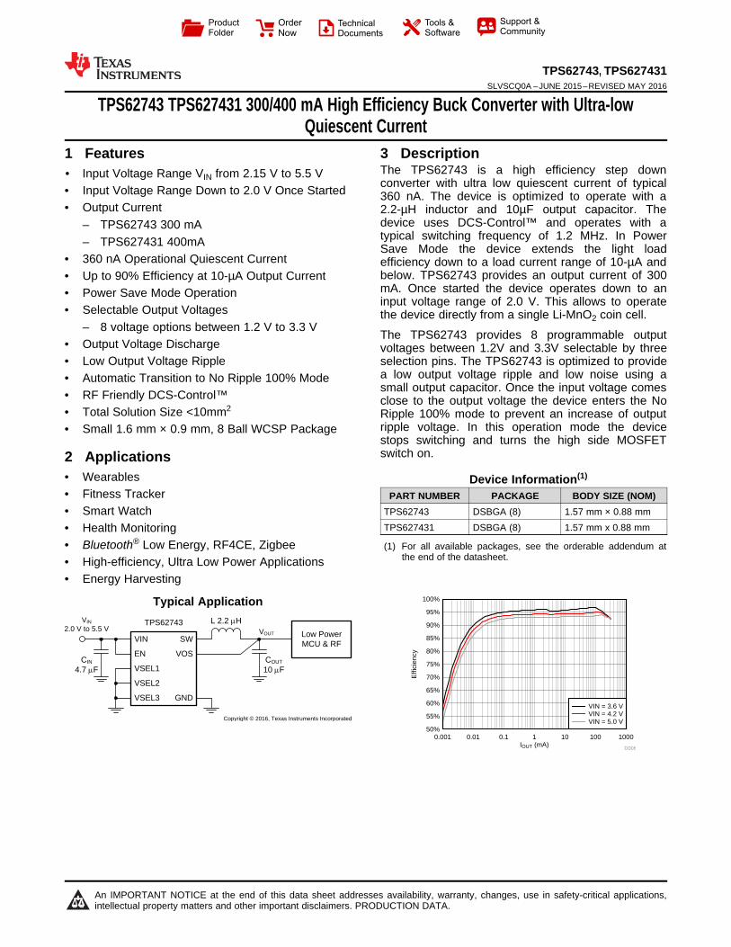
TPS62743 TPS627431 300/400 mA High Efficiency Buck Converter with Ultra-lowQuiescent Current
1
1 Features1• Input Voltage Range VIN from 2.15 V to 5.5 V• Input Voltage Range Down to 2.0 V Once Started• Output Current
– TPS62743 300 mA– TPS627431 400mA
• 360 nA Operational Quiescent Current• Up to 90% Efficiency at 10-µA Output Current• Power Save Mode Operation• Selectable Output Voltages
– 8 voltage options between 1.2 V to 3.3 V• Output Voltage Discharge• Low Output Voltage Ripple• Automatic Transition to No Ripple 100% Mode• RF Friendly DCS-Control™• Total Solution Size <10mm2
• Small 1.6 mm × 0.9 mm, 8 Ball WCSP Package
2 Applications• Wearables• Fitness Tracker• Smart Watch• Health Monitoring• Bluetooth® Low Energy, RF4CE, Zigbee• High-efficiency, Ultra Low Power Applications• Energy Harvesting
3 DescriptionThe TPS62743 is a high efficiency step downconverter with ultra low quiescent current of typical360 nA. The device is optimized to operate with a2.2-µH inductor and 10µF output capacitor. Thedevice uses DCS-Control™ and operates with atypical switching frequency of 1.2 MHz. In PowerSave Mode the device extends the light loadefficiency down to a load current range of 10-µA andbelow. TPS62743 provides an output current of 300mA. Once started the device operates down to aninput voltage range of 2.0 V. This allows to operatethe device directly from a single Li-MnO2 coin cell.
The TPS62743 provides 8 programmable outputvoltages between 1.2V and 3.3V selectable by threeselection pins. The TPS62743 is optimized to providea low output voltage ripple and low noise using asmall output capacitor. Once the input voltage comesclose to the output voltage the device enters the NoRipple 100% mode to prevent an increase of outputripple voltage. In this operation mode the devicestops switching and turns the high side MOSFETswitch on.
Device Information(1)
PART NUMBER PACKAGE BODY SIZE (NOM)TPS62743 DSBGA (8) 1.57 mm × 0.88 mmTPS627431 DSBGA (8) 1.57 mm x 0.88 mm
(1) For all available packages, see the orderable addendum atthe end of the datasheet.
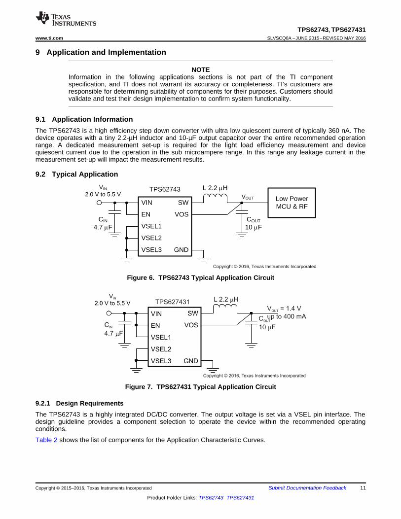
Typical Application
2
TPS62743, TPS627431SLVSCQ0A –JUNE 2015–REVISED MAY 2016 www.ti.com
Product Folder Links: TPS62743 TPS627431
Submit Documentation Feedback Copyright © 2015–2016, Texas Instruments Incorporated
Table of Contents1 Features .................................................................. 12 Applications ........................................................... 13 Description ............................................................. 14 Revision History..................................................... 25 Device Comparison Table ..................................... 36 Pin Configuration and Functions ......................... 37 Specifications......................................................... 4
7.1 Absolute Maximum Ratings ...................................... 47.2 ESD Ratings ............................................................ 47.3 Recommended Operating Conditions....................... 47.4 Thermal Information ................................................. 57.5 Electrical Characteristics........................................... 57.6 Timing Requirements ................................................ 67.7 Typical Characteristics .............................................. 7
8 Detailed Description .............................................. 88.1 Overview ................................................................... 88.2 Functional Block Diagram ......................................... 88.3 Feature Description................................................... 8
8.4 Device Functional Modes........................................ 109 Application and Implementation ........................ 11
9.1 Application Information............................................ 119.2 Typical Application ................................................. 119.3 System Example ..................................................... 17
10 Power Supply Recommendations ..................... 1811 Layout................................................................... 18
11.1 Layout Guidelines ................................................. 1811.2 Layout Example .................................................... 18
12 Device and Documentation Support ................. 1912.1 Device Support...................................................... 1912.2 Related Links ........................................................ 1912.3 Community Resources.......................................... 1912.4 Trademarks ........................................................... 1912.5 Electrostatic Discharge Caution............................ 1912.6 Glossary ................................................................ 19
13 Mechanical, Packaging, and OrderableInformation ........................................................... 19
4 Revision HistoryNOTE: Page numbers for previous revisions may differ from page numbers in the current version.
Changes from Original (June 2015) to Revision A Page
• Added TPS627431 device to data sheet ............................................................................................................................... 1• Added device option TPS627431: 400mA output current, other output voltages than TPS62743 ........................................ 1• Added TPS627431 to Device Comparison Table .................................................................................................................. 3• Added Figure 7 .................................................................................................................................................................... 11
1 2
A
B
C
D
SW VIN
EN GND
VOSVSEL1
VSEL2 VSEL3
3
TPS62743, TPS627431www.ti.com SLVSCQ0A –JUNE 2015–REVISED MAY 2016
Product Folder Links: TPS62743 TPS627431
Submit Documentation FeedbackCopyright © 2015–2016, Texas Instruments Incorporated
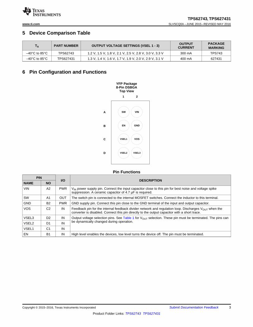
5 Device Comparison Table
TA PART NUMBER OUTPUT VOLTAGE SETTINGS (VSEL 1 - 3) OUTPUTCURRENT
PACKAGEMARKING
–40°C to 85°C TPS62743 1.2 V, 1.5 V, 1.8 V, 2.1 V, 2.5 V, 2.8 V, 3.0 V, 3.3 V 300 mA TPS743–40°C to 85°C TPS627431 1.3 V, 1.4 V, 1.6 V, 1.7 V, 1.9 V, 2.0 V, 2.9 V, 3.1 V 400 mA 627431
6 Pin Configuration and Functions
YFP Package8-Pin DSBGA
Top View
Pin FunctionsPIN
I/O DESCRIPTIONNAME NOVIN A2 PWR VIN power supply pin. Connect the input capacitor close to this pin for best noise and voltage spike
suppression. A ceramic capacitor of 4.7 µF is required.SW A1 OUT The switch pin is connected to the internal MOSFET switches. Connect the inductor to this terminal.GND B2 PWR GND supply pin. Connect this pin close to the GND terminal of the input and output capacitor.VOS C2 IN Feedback pin for the internal feedback divider network and regulation loop. Discharges VOUT when the
converter is disabled. Connect this pin directly to the output capacitor with a short trace.VSEL3 D2 IN Output voltage selection pins. See Table 1 for VOUT selection. These pin must be terminated. The pins can
be dynamically changed during operation.VSEL2 D1 INVSEL1 C1 INEN B1 IN High level enables the devices, low level turns the device off. The pin must be terminated.
4
TPS62743, TPS627431SLVSCQ0A –JUNE 2015–REVISED MAY 2016 www.ti.com
Product Folder Links: TPS62743 TPS627431
Submit Documentation Feedback Copyright © 2015–2016, Texas Instruments Incorporated
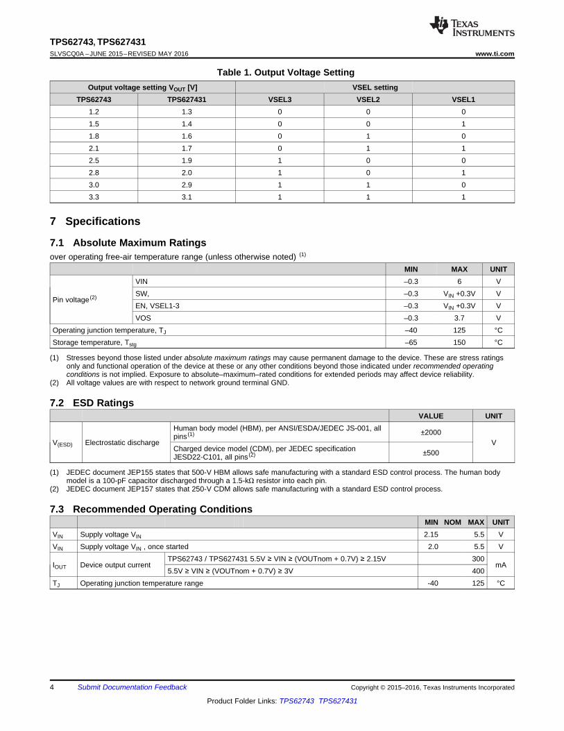
Table 1. Output Voltage SettingOutput voltage setting VOUT [V] VSEL setting
TPS62743 TPS627431 VSEL3 VSEL2 VSEL11.2 1.3 0 0 01.5 1.4 0 0 11.8 1.6 0 1 02.1 1.7 0 1 12.5 1.9 1 0 02.8 2.0 1 0 13.0 2.9 1 1 03.3 3.1 1 1 1
(1) Stresses beyond those listed under absolute maximum ratings may cause permanent damage to the device. These are stress ratingsonly and functional operation of the device at these or any other conditions beyond those indicated under recommended operatingconditions is not implied. Exposure to absolute–maximum–rated conditions for extended periods may affect device reliability.
(2) All voltage values are with respect to network ground terminal GND.
7 Specifications
7.1 Absolute Maximum Ratingsover operating free-air temperature range (unless otherwise noted) (1)
MIN MAX UNIT
Pin voltage (2)
VIN –0.3 6 VSW, –0.3 VIN +0.3V VEN, VSEL1-3 –0.3 VIN +0.3V VVOS –0.3 3.7 V
Operating junction temperature, TJ –40 125 °CStorage temperature, Tstg –65 150 °C
(1) JEDEC document JEP155 states that 500-V HBM allows safe manufacturing with a standard ESD control process. The human bodymodel is a 100-pF capacitor discharged through a 1.5-kΩ resistor into each pin.
(2) JEDEC document JEP157 states that 250-V CDM allows safe manufacturing with a standard ESD control process.
7.2 ESD RatingsVALUE UNIT
V(ESD) Electrostatic discharge
Human body model (HBM), per ANSI/ESDA/JEDEC JS-001, allpins (1) ±2000
VCharged device model (CDM), per JEDEC specificationJESD22-C101, all pins (2) ±500
7.3 Recommended Operating ConditionsMIN NOM MAX UNIT
VIN Supply voltage VIN 2.15 5.5 VVIN Supply voltage VIN , once started 2.0 5.5 V
IOUT Device output currentTPS62743 / TPS627431 5.5V ≥ VIN ≥ (VOUTnom + 0.7V) ≥ 2.15V 300
mA5.5V ≥ VIN ≥ (VOUTnom + 0.7V) ≥ 3V 400
TJ Operating junction temperature range -40 125 °C
5
TPS62743, TPS627431www.ti.com SLVSCQ0A –JUNE 2015–REVISED MAY 2016
Product Folder Links: TPS62743 TPS627431
Submit Documentation FeedbackCopyright © 2015–2016, Texas Instruments Incorporated
(1) For more information about traditional and new thermal metrics, see the Semiconductor and IC Package Thermal Metrics applicationreport, SPRA953.
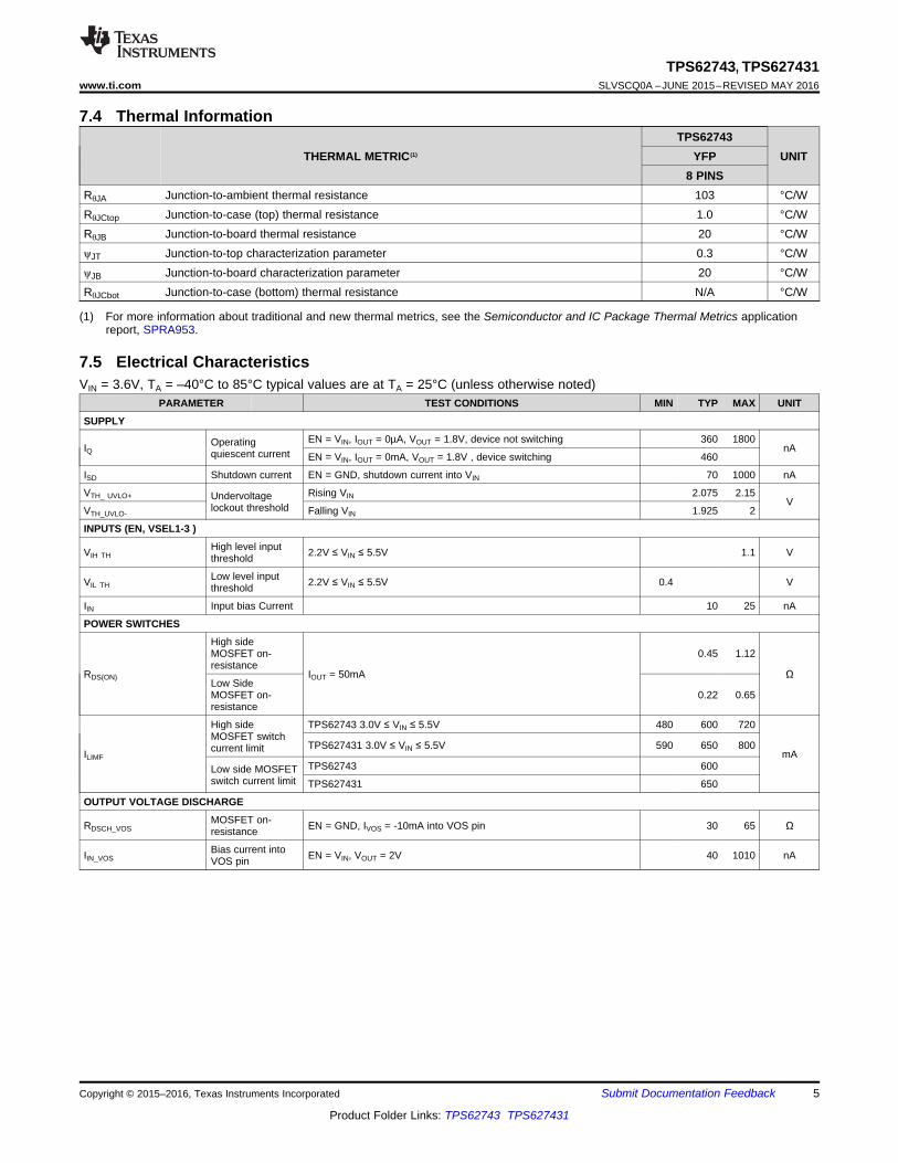
7.4 Thermal Information
THERMAL METRIC (1)
TPS62743UNITYFP
8 PINSRθJA Junction-to-ambient thermal resistance 103 °C/WRθJCtop Junction-to-case (top) thermal resistance 1.0 °C/WRθJB Junction-to-board thermal resistance 20 °C/WψJT Junction-to-top characterization parameter 0.3 °C/WψJB Junction-to-board characterization parameter 20 °C/WRθJCbot Junction-to-case (bottom) thermal resistance N/A °C/W
7.5 Electrical CharacteristicsVIN = 3.6V, TA = –40°C to 85°C typical values are at TA = 25°C (unless otherwise noted)
PARAMETER TEST CONDITIONS MIN TYP MAX UNIT
SUPPLY
IQOperatingquiescent current
EN = VIN, IOUT = 0µA, VOUT = 1.8V, device not switching 360 1800nA
EN = VIN, IOUT = 0mA, VOUT = 1.8V , device switching 460
ISD Shutdown current EN = GND, shutdown current into VIN 70 1000 nA
VTH_ UVLO+ Undervoltagelockout threshold
Rising VIN 2.075 2.15V
VTH_UVLO- Falling VIN 1.925 2
INPUTS (EN, VSEL1-3 )
VIH THHigh level inputthreshold 2.2V ≤ VIN ≤ 5.5V 1.1 V
VIL THLow level inputthreshold 2.2V ≤ VIN ≤ 5.5V 0.4 V
IIN Input bias Current 10 25 nA
POWER SWITCHES
RDS(ON)
High sideMOSFET on-resistance
IOUT = 50mA
0.45 1.12
ΩLow SideMOSFET on-resistance
0.22 0.65
ILIMF
High sideMOSFET switchcurrent limit
TPS62743 3.0V ≤ VIN ≤ 5.5V 480 600 720
mATPS627431 3.0V ≤ VIN ≤ 5.5V 590 650 800
Low side MOSFETswitch current limit
TPS62743 600
TPS627431 650
OUTPUT VOLTAGE DISCHARGE
RDSCH_VOSMOSFET on-resistance EN = GND, IVOS = -10mA into VOS pin 30 65 Ω
IIN_VOSBias current intoVOS pin EN = VIN, VOUT = 2V 40 1010 nA
6
TPS62743, TPS627431SLVSCQ0A –JUNE 2015–REVISED MAY 2016 www.ti.com
Product Folder Links: TPS62743 TPS627431
Submit Documentation Feedback Copyright © 2015–2016, Texas Instruments Incorporated
Electrical Characteristics (continued)VIN = 3.6V, TA = –40°C to 85°C typical values are at TA = 25°C (unless otherwise noted)
PARAMETER TEST CONDITIONS MIN TYP MAX UNIT
(1) VIN is compared to the programmed output voltage (VOUT). When VIN–VOUT falls below VTH_100- the device enters 100% Mode by turningthe high side MOSFET on. The 100% Mode is exited when VIN–VOUT exceeds VTH_100+ and the device starts switching. The hysteresisfor the 100% Mode detection threshold VTH_100+ - VTH_100- will always be positive and will be approximately 50 mV(typ)
AUTO 100% MODE TRANSITION
VTH_100+
Auto 100% Modeleave detectionthreshold (1)
Rising VIN,100% Mode is left with VIN = VOUT + VTH_100+ 150 250 350
mV
VTH_100-
Auto 100% Modeenter detectionthreshold (1)
Falling VIN, 100% Mode is entered with VIN = VOUT + VTH_100- 85 200 290
OUTPUT
ILIM_softstart
High side softstartswitch current limit
EN=low to high80 150 200
mALow side softstartswitch current limit 150
VOUT
Output voltagerange Output voltages are selected with pins VSEL 1 - 3 1.2 3.3
VOutput voltageaccuracy
IOUT = 10mA, VOUT = 1.8V -2.5 0% 2.5
IOUT = 100mA, VOUT = 1.8V –2 0% 2
DC output voltageload regulation VOUT = 1.8V 0.001 %/mA
DC output voltageline regulation VOUT = 1.8V, IOUT = 100mA, 2.2V ≤ VIN ≤ 5.0V 0 %/V
7.6 Timing RequirementsVIN = 3.6V, TJ = –40°C to 85°C typical values are at TA = 25°C (unless otherwise noted)
PARAMETER TEST CONDITIONS MIN TYP MAX UNIT
OUTPUT
tONmin Minimum ON time VOUT = 2.0V, IOUT = 0 mA 225 ns
tOFFmin Minimum OFF time VIN = 2.3V 50 ns
tStartup_delayRegulator start updelay time From transition EN = low to high until device starts switching 10 25 ms
tSoftstart Softstart time 2.2V ≤ VIN ≤ 5.5V, EN = VIN 700 1200 µs
Temperature (qC)
Hig
h S
ide
RD
SO
N (:
)
-60 -40 -20 0 20 40 60 80 1000
0.1
0.2
0.3
0.4
0.5
0.6
0.7
0.8
0.9
1
D003
VIN = 2.2 VVIN = 2.5 VVIN = 3.6 V
Temperature (qC)
Low
Sid
e R
DS
ON
(:
)
-60 -40 -20 0 20 40 60 80 1000
0.05
0.1
0.15
0.2
0.25
0.3
0.35
0.4
0.45
0.5
D004
VIN = 2.2 VVIN = 2.5 VVIN = 3.6 V
Temperature (qC)
Qui
esce
nt C
urre
nt (
nA)
-60 -40 -20 0 20 40 60 80 100200
300
400
500
600
700
D001
VIN = 2.2 VVIN = 2.5 VVIN = 3.6 VVIN = 5.5 VVIN = 6.0 V
Temperature (qC)
Shu
tdow
n C
urre
nt (
nA)
-60 -40 -20 0 20 40 60 80 1000
25
50
75
100
125
150
175
200
225
250
D002
VIN = 2.2 VVIN = 2.5 VVIN = 3.6 VVIN = 5.5 VVIN = 6.0 V
7
TPS62743, TPS627431www.ti.com SLVSCQ0A –JUNE 2015–REVISED MAY 2016
Product Folder Links: TPS62743 TPS627431
Submit Documentation FeedbackCopyright © 2015–2016, Texas Instruments Incorporated
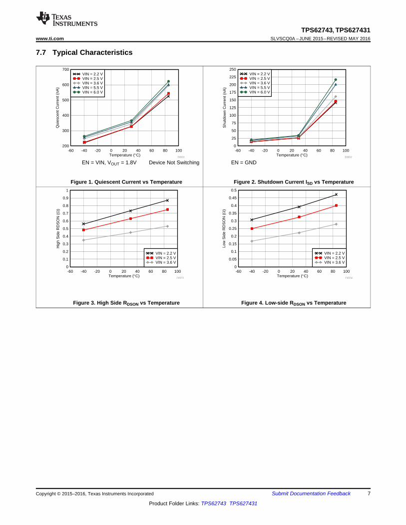
7.7 Typical Characteristics
EN = VIN, VOUT = 1.8V Device Not Switching
Figure 1. Quiescent Current vs Temperature
EN = GND
Figure 2. Shutdown Current ISD vs Temperature
Figure 3. High Side RDSON vs Temperature Figure 4. Low-side RDSON vs Temperature
UVLO
EN
Gate DriverAnti
Shoot-Through
CurrentLimit Comparator
SW
LimitHigh Side
VIN
GND
PMOS
NMOS
VTH_UVLO
VIN
UVLOComp
Softstart
ControlLogic
VOS
VFB
MainComparator
Direct Control& Compensation
Erroramplifier
Min. On
Min. OFF
VIN
VOS
Timer
DCSControl
Current
Limit Comparator
LimitLow Side
Power Stage
UVLO
VOS
Internalfeedback
dividernetwork*
VSEL1
VSEL2
VSEL3
Ultra Low PowerReference
VTH_100
VIN
Auto 100% ModeComp
100%Mode
V
DischargeOUT
VFB
UVLO
EN
EN
VOS
* typical 50MW
VREF
Copyright © 2016, Texas Instruments Incorporated
8
TPS62743, TPS627431SLVSCQ0A –JUNE 2015–REVISED MAY 2016 www.ti.com
Product Folder Links: TPS62743 TPS627431
Submit Documentation Feedback Copyright © 2015–2016, Texas Instruments Incorporated
8 Detailed Description
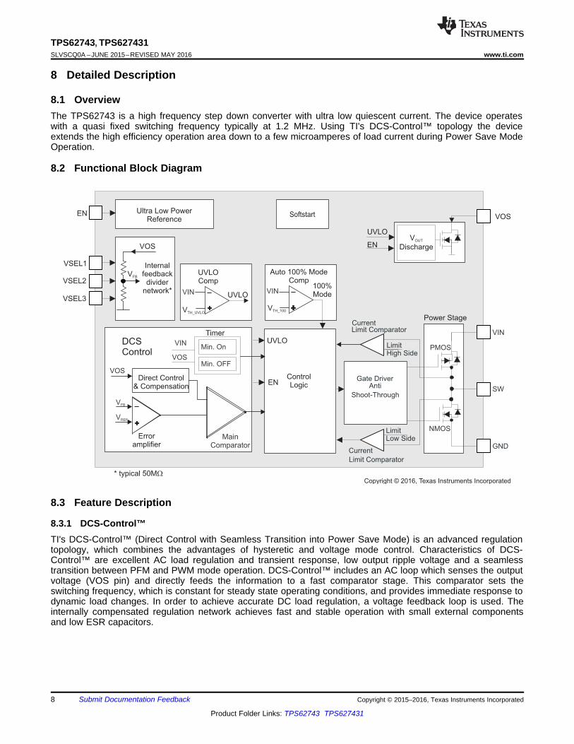
8.1 OverviewThe TPS62743 is a high frequency step down converter with ultra low quiescent current. The device operateswith a quasi fixed switching frequency typically at 1.2 MHz. Using TI's DCS-Control™ topology the deviceextends the high efficiency operation area down to a few microamperes of load current during Power Save ModeOperation.
8.2 Functional Block Diagram
8.3 Feature Description
8.3.1 DCS-Control™TI's DCS-Control™ (Direct Control with Seamless Transition into Power Save Mode) is an advanced regulationtopology, which combines the advantages of hysteretic and voltage mode control. Characteristics of DCS-Control™ are excellent AC load regulation and transient response, low output ripple voltage and a seamlesstransition between PFM and PWM mode operation. DCS-Control™ includes an AC loop which senses the outputvoltage (VOS pin) and directly feeds the information to a fast comparator stage. This comparator sets theswitching frequency, which is constant for steady state operating conditions, and provides immediate response todynamic load changes. In order to achieve accurate DC load regulation, a voltage feedback loop is used. Theinternally compensated regulation network achieves fast and stable operation with small external componentsand low ESR capacitors.
9
TPS62743, TPS627431www.ti.com SLVSCQ0A –JUNE 2015–REVISED MAY 2016
Product Folder Links: TPS62743 TPS627431
Submit Documentation FeedbackCopyright © 2015–2016, Texas Instruments Incorporated
Feature Description (continued)The DCS-Control™ topology supports PWM (Pulse Width Modulation) mode for medium and high loadconditions and a Power Save Mode at light loads. During PWM mode, it operates in continuous conductionmode. The switching frequency is typically 1.2 MHz with a controlled frequency variation depending on the inputvoltage and load current. If the load current decreases, the converter seamlessly enters Power Save Mode tomaintain high efficiency down to very light loads. In Power Save Mode, the switching frequency varies linearlywith the load current. Since DCS-Control™ supports both operation modes within one single building block, thetransition from PWM to Power Save Mode is seamless with minimum output voltage ripple. The TPS62743 offersboth excellent DC voltage and superior load transient regulation, combined with low output voltage ripple,minimizing interference with RF circuits.
8.3.2 Power Save Mode OperationIn Power Save Mode the device operates in PFM (Pulse Frequency Modulation) that generates a singleswitching pulse to ramp up the inductor current and recharges the output capacitor, followed by a sleep periodwhere most of the internal circuits are shutdown to achieve lowest operating quiescent current. During this time,the load current is supported by the output capacitor. The duration of the sleep period depends on the loadcurrent and the inductor peak current. During the sleep periods, the current consumption of TPS62743 isreduced to 360 nA. This low quiescent current consumption is achieved by an ultra low power voltage reference,an integrated high impedance feedback divider network and an optimized Power Save Mode operation.
8.3.3 Output Voltage SelectionThe TPS62743 doesn't require an external resistor divider network to program the output voltage. The deviceintegrates a high impedance feedback resistor divider network that is programmed by the pins VSEL1-3.TPS62743 supports an output voltage range from 1.2 V to 3.3 V. The output voltage is programmed according toTable 1. The output voltage can be changed during operation. This can be used for simple dynamic outputvoltage scaling.
8.3.4 Output Voltage Discharge of the Buck ConverterThe device provides automatic output voltage discharge when EN is pulled low or the UVLO is triggered. Theoutput of the buck converter is discharged over VOS. Because of this the output voltage will ramp up from zeroonce the device is enabled again. This is very helpful for accurate start-up sequencing.
8.3.5 Undervoltage Lockout UVLOTo avoid misoperation of the device at low input voltages, an undervoltage lockout is used. The UVLO shutsdown the device at a maximum voltage level of 2.0 V. The device will start at a UVLO level of 2.15 V.
8.3.6 Short circuit protectionThe TPS6274x integrates a current limit on the high side, as well on the low side MOSFETs to protect the deviceagainst overload or short circuit conditions. The peak current in the switches is monitored cycle by cycle. If thehigh side MOSFET current limit is reached, the high side MOSFET is turned off and the low side MOSFET isturned on until the switch current decreases below the low side MOSFET current limit. Once the low sideMOSFET current limit trips, the low side MOSFET is turned off and the high side MOSFET turns on again.
V ,IN
VOUT
tsoftstart
VIN
Step Down Operation
100%Mode
100%Mode
VTH_100+
VTH_100-
VUVLO+
VUVLO-
V
tracks VOUT
IN
V
tracks VOUT
IN
V
dischargeOUT
10
TPS62743, TPS627431SLVSCQ0A –JUNE 2015–REVISED MAY 2016 www.ti.com
Product Folder Links: TPS62743 TPS627431
Submit Documentation Feedback Copyright © 2015–2016, Texas Instruments Incorporated
8.4 Device Functional Modes
8.4.1 Enable and ShutdownThe device is turned on with EN=high. With EN=low the device enters shutdown. This pin must be terminated.
8.4.2 Device Start-up and SoftstartThe device has an internal softstart to minimize input voltage drop during start-up. This allows the operation fromhigh impedance battery cells. Once the device is enabled the device starts switching after a typical delay time of10ms. Then the softstart time of typical 700 µs begins with a reduced current limit of typical 150 mA. When thistime passed by the device enters full current limit operation. This allows a smooth start-up and the device canstart into full load current. Furthermore, larger output capacitors impact the start-up behaviour of the DC/DCconverter. Especially when the output voltage does not reach its nominal value after the typical soft-start time of700 µs, has passed.
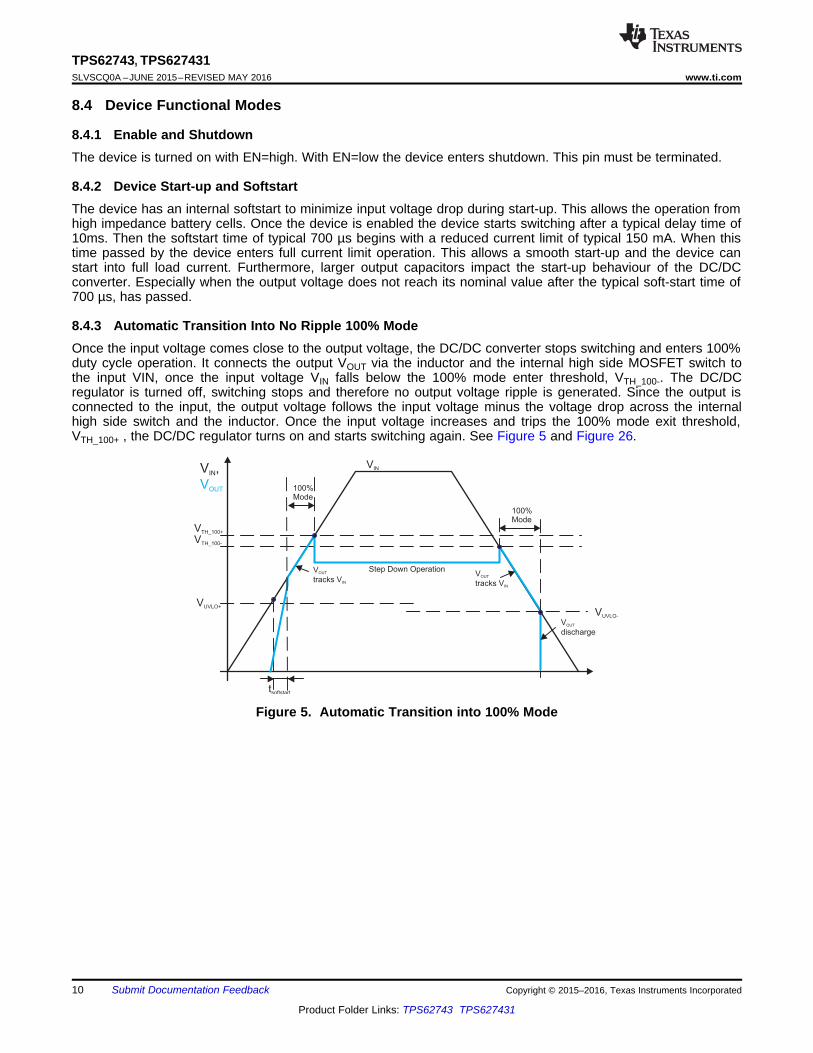
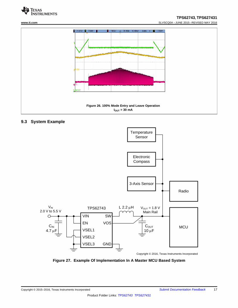
8.4.3 Automatic Transition Into No Ripple 100% ModeOnce the input voltage comes close to the output voltage, the DC/DC converter stops switching and enters 100%duty cycle operation. It connects the output VOUT via the inductor and the internal high side MOSFET switch tothe input VIN, once the input voltage VIN falls below the 100% mode enter threshold, VTH_100-. The DC/DCregulator is turned off, switching stops and therefore no output voltage ripple is generated. Since the output isconnected to the input, the output voltage follows the input voltage minus the voltage drop across the internalhigh side switch and the inductor. Once the input voltage increases and trips the 100% mode exit threshold,VTH_100+ , the DC/DC regulator turns on and starts switching again. See Figure 5 and Figure 26.
Figure 5. Automatic Transition into 100% Mode
L 2.2 Hm
C
4.7IN
mF
C
10 FOUT
m
TPS627431V = 1.4 V
up to 400 mAOUT
VIN
EN
VSEL1
VSEL2
VSEL3
SW
VOS
GND
V
2.0 V to 5.5 VIN
Copyright © 2016, Texas Instruments Incorporated
VIN
EN
VSEL1
VSEL2
VSEL3
SW
VOS
GND
L 2.2 PH
COUT
10 PFCIN
4.7 PF
VIN
2.0 V to 5.5 VLow Power MCU & RF
TPS62743VOUT
Copyright © 2016, Texas Instruments Incorporated
11
TPS62743, TPS627431www.ti.com SLVSCQ0A –JUNE 2015–REVISED MAY 2016
Product Folder Links: TPS62743 TPS627431
Submit Documentation FeedbackCopyright © 2015–2016, Texas Instruments Incorporated
9 Application and Implementation
NOTEInformation in the following applications sections is not part of the TI componentspecification, and TI does not warrant its accuracy or completeness. TI’s customers areresponsible for determining suitability of components for their purposes. Customers shouldvalidate and test their design implementation to confirm system functionality.
9.1 Application InformationThe TPS62743 is a high efficiency step down converter with ultra low quiescent current of typically 360 nA. Thedevice operates with a tiny 2.2-µH inductor and 10-µF output capacitor over the entire recommended operationrange. A dedicated measurement set-up is required for the light load efficiency measurement and devicequiescent current due to the operation in the sub microampere range. In this range any leakage current in themeasurement set-up will impact the measurement results.
9.2 Typical Application
Figure 6. TPS62743 Typical Application Circuit
Figure 7. TPS627431 Typical Application Circuit
9.2.1 Design RequirementsThe TPS62743 is a highly integrated DC/DC converter. The output voltage is set via a VSEL pin interface. Thedesign guideline provides a component selection to operate the device within the recommended operatingconditions.
Table 2 shows the list of components for the Application Characteristic Curves.
LLmax outmax
II = I +
2
D
L
Vout1
VinI = Vout
L
-
D ´´ ¦
12
TPS62743, TPS627431SLVSCQ0A –JUNE 2015–REVISED MAY 2016 www.ti.com
Product Folder Links: TPS62743 TPS627431
Submit Documentation Feedback Copyright © 2015–2016, Texas Instruments Incorporated
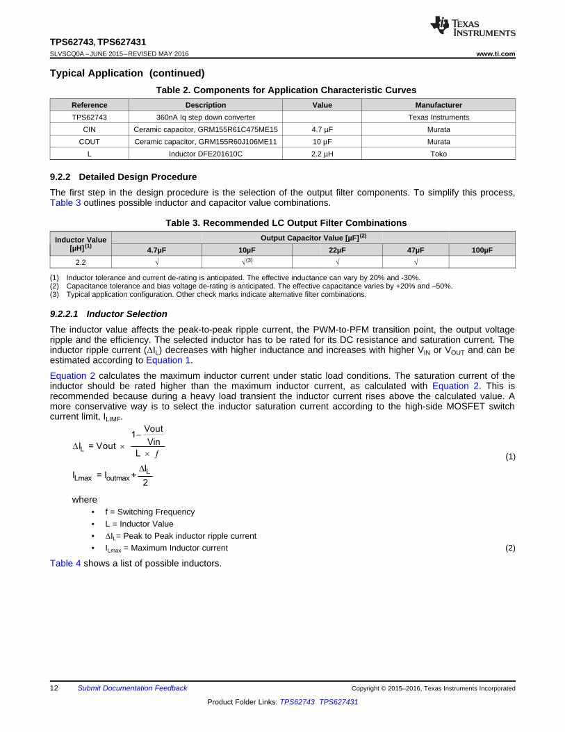
Typical Application (continued)Table 2. Components for Application Characteristic Curves
Reference Description Value ManufacturerTPS62743 360nA Iq step down converter Texas Instruments
CIN Ceramic capacitor, GRM155R61C475ME15 4.7 µF MurataCOUT Ceramic capacitor, GRM155R60J106ME11 10 µF Murata
L Inductor DFE201610C 2.2 µH Toko
(1) Inductor tolerance and current de-rating is anticipated. The effective inductance can vary by 20% and -30%.(2) Capacitance tolerance and bias voltage de-rating is anticipated. The effective capacitance varies by +20% and –50%.(3) Typical application configuration. Other check marks indicate alternative filter combinations.
9.2.2 Detailed Design ProcedureThe first step in the design procedure is the selection of the output filter components. To simplify this process,Table 3 outlines possible inductor and capacitor value combinations.
Table 3. Recommended LC Output Filter Combinations
Inductor Value[µH] (1)
Output Capacitor Value [µF] (2)
4.7µF 10µF 22µF 47µF 100µF2.2 √ √ (3) √ √
9.2.2.1 Inductor SelectionThe inductor value affects the peak-to-peak ripple current, the PWM-to-PFM transition point, the output voltageripple and the efficiency. The selected inductor has to be rated for its DC resistance and saturation current. Theinductor ripple current (ΔIL) decreases with higher inductance and increases with higher VIN or VOUT and can beestimated according to Equation 1.
Equation 2 calculates the maximum inductor current under static load conditions. The saturation current of theinductor should be rated higher than the maximum inductor current, as calculated with Equation 2. This isrecommended because during a heavy load transient the inductor current rises above the calculated value. Amore conservative way is to select the inductor saturation current according to the high-side MOSFET switchcurrent limit, ILIMF.
(1)
where• f = Switching Frequency• L = Inductor Value• ΔIL= Peak to Peak inductor ripple current• ILmax = Maximum Inductor current (2)
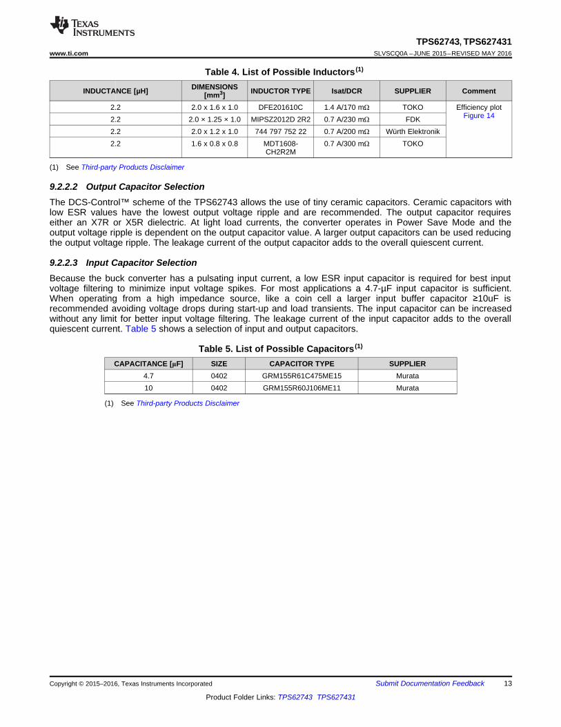
Table 4 shows a list of possible inductors.
13
TPS62743, TPS627431www.ti.com SLVSCQ0A –JUNE 2015–REVISED MAY 2016
Product Folder Links: TPS62743 TPS627431
Submit Documentation FeedbackCopyright © 2015–2016, Texas Instruments Incorporated
(1) See Third-party Products Disclaimer
Table 4. List of Possible Inductors (1)
INDUCTANCE [µH] DIMENSIONS[mm3] INDUCTOR TYPE Isat/DCR SUPPLIER Comment
2.2 2.0 x 1.6 x 1.0 DFE201610C 1.4 A/170 mΩ TOKO Efficiency plotFigure 142.2 2.0 × 1.25 × 1.0 MIPSZ2012D 2R2 0.7 A/230 mΩ FDK
2.2 2.0 x 1.2 x 1.0 744 797 752 22 0.7 A/200 mΩ Würth Elektronik2.2 1.6 x 0.8 x 0.8 MDT1608-
CH2R2M0.7 A/300 mΩ TOKO
9.2.2.2 Output Capacitor SelectionThe DCS-Control™ scheme of the TPS62743 allows the use of tiny ceramic capacitors. Ceramic capacitors withlow ESR values have the lowest output voltage ripple and are recommended. The output capacitor requireseither an X7R or X5R dielectric. At light load currents, the converter operates in Power Save Mode and theoutput voltage ripple is dependent on the output capacitor value. A larger output capacitors can be used reducingthe output voltage ripple. The leakage current of the output capacitor adds to the overall quiescent current.
9.2.2.3 Input Capacitor SelectionBecause the buck converter has a pulsating input current, a low ESR input capacitor is required for best inputvoltage filtering to minimize input voltage spikes. For most applications a 4.7-µF input capacitor is sufficient.When operating from a high impedance source, like a coin cell a larger input buffer capacitor ≥10uF isrecommended avoiding voltage drops during start-up and load transients. The input capacitor can be increasedwithout any limit for better input voltage filtering. The leakage current of the input capacitor adds to the overallquiescent current. Table 5 shows a selection of input and output capacitors.
(1) See Third-party Products Disclaimer
Table 5. List of Possible Capacitors (1)
CAPACITANCE [μF] SIZE CAPACITOR TYPE SUPPLIER4.7 0402 GRM155R61C475ME15 Murata10 0402 GRM155R60J106ME11 Murata
IOUT (mA)
Effi
cien
cy
0.001 0.01 0.1 1 10 100 100040%
45%
50%
55%
60%
65%
70%
75%
80%
85%
90%
D009
VIN = 2.5 VVIN = 3.0 VVIN = 3.6 VVIN = 4.2 VVIN = 5.0 V
30
40
50
60
70
80
90
0.001 0.01 0.1 1 10 100 1000
Effic
iency [%
]
I [mA]OUT
V = 5.0VIN
V =IN 4.2V
V =IN 3.6V
V =IN 3.0V
V =IN 2.6V
IOUT (mA)
Effi
cien
cy
0.001 0.01 0.1 1 10 100 100040%
45%
50%
55%
60%
65%
70%
75%
80%
85%
90%
95%
100%
D008
VIN = 2.5 VVIN = 3.0 VVIN = 3.6 VVIN = 4.2 VVIN = 5.0 V
Effic
iency [%
]
I [mA]OUT
30
40
50
60
70
80
90
100
0.001 0.01 0.1 1 10 100 1000
C001
V = 5.0VIN
V =IN 4.2V
V =IN 3.6V
V =IN 3.0V
V =IN 2.6V
IOUT (mA)
Effi
cien
cy
0.001 0.01 0.1 1 10 100 100050%
55%
60%
65%
70%
75%
80%
85%
90%
95%
100%
D006
VIN = 3.6 VVIN = 4.2 VVIN = 5.0 V
IOUT (mA)
Effi
cien
cy
0.001 0.01 0.1 1 10 100 100040%
45%
50%
55%
60%
65%
70%
75%
80%
85%
90%
95%
100%
D007
VIN = 2.5 VVIN = 3.0 VVIN = 3.6 VVIN = 4.2 VVIN = 5.0 V
14
TPS62743, TPS627431SLVSCQ0A –JUNE 2015–REVISED MAY 2016 www.ti.com
Product Folder Links: TPS62743 TPS627431
Submit Documentation Feedback Copyright © 2015–2016, Texas Instruments Incorporated
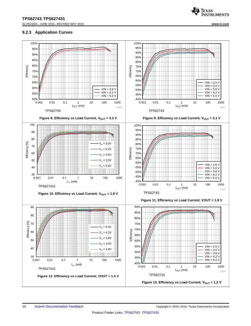
9.2.3 Application Curves
TPS62743
Figure 8. Efficiency vs Load Current, VOUT = 3.3 V
TPS62743
Figure 9. Efficiency vs Load Current; VOUT = 2.1 V
TPS627431
Figure 10. Efficiency vs Load Current; VOUT = 1.9 V TPS62743
Figure 11. Efficiency vs Load Current; VOUT = 1.8 V
TPS627431
Figure 12. Efficiency vs Load Current; VOUT = 1.4 V TPS62743
Figure 13. Efficiency vs Load Current; VOUT = 1.2 V
IOUT (mA)
Sw
itchi
ng F
requ
ency
(kH
z)
0 50 100 150 200 250 300 3500
200
400
600
800
1000
1200
1400
D013
VIN = 5.0 VVIN = 3.6 VVIN = 3.0 VVIN = 2.0 V
0
5
10
15
20
25
30
35
40
45
50
0.01 0.1 1 10 100 1000
V[m
Vp
p]
OU
Tpp
I [mA]OUT C001
V = 4.2VIN
V = 3.6VIN
V = 3.0VINC001
IOUT (mA)
Sw
itchi
ng F
requ
ency
(kH
z)
0 50 100 150 200 250 300 3500
200
400
600
800
1000
1200
1400
1600
D012
VIN = 5.0 VVIN = 3.6 VVIN = 3.0 VVIN = 2.2 V
I [mA]OUT
Sw
itchin
g F
requency [kH
z]
0
200
400
600
800
1000
1200
1400
0 50 100 150 200 250 300 350 400 450
C002
V = 5.0VIN
V =IN 4.2V
V =IN 3.6V
V =IN 3.0V
V =IN 2.6V
IOUT (mA)
Effi
cien
cy
0.001 0.01 0.1 1 10 100 100050%
55%
60%
65%
70%
75%
80%
85%
90%
95%
D010
DEF201610MIPSZ2012WE 744 797 752 22MDT1608
IOUT (mA)
Sw
itchi
ng F
requ
ency
(kH
z)
0 50 100 150 200 250 300 3500
200
400
600
800
1000
1200
1400
1600
1800
D011
VIN = 5.0 VVIN = 3.6 V
15
TPS62743, TPS627431www.ti.com SLVSCQ0A –JUNE 2015–REVISED MAY 2016
Product Folder Links: TPS62743 TPS627431
Submit Documentation FeedbackCopyright © 2015–2016, Texas Instruments Incorporated
TPS62743
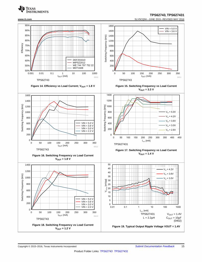
Figure 14. Efficiency vs Load Current; VOUT = 1.8 V
TPS62743
Figure 15. Switching Frequency vs Load CurrentVOUT = 3.3 V
TPS62743
Figure 16. Switching Frequency vs Load CurrentVOUT = 1.8 V
TPS627431
Figure 17. Switching Frequency vs Load CurrentVOUT = 1.4 V
TPS62743
Figure 18. Switching Frequency vs Load CurrentVOUT = 1.2 V
TPS627431 VOUT = 1.4VL = 2.2µH COUT = 10µF
(0402)
Figure 19. Typical Output Ripple Voltage VOUT = 1.4V
IL
IL
IL
IL
16
TPS62743, TPS627431SLVSCQ0A –JUNE 2015–REVISED MAY 2016 www.ti.com
Product Folder Links: TPS62743 TPS627431
Submit Documentation Feedback Copyright © 2015–2016, Texas Instruments Incorporated
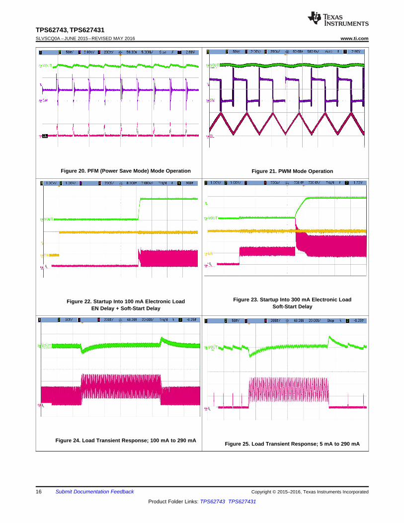
Figure 20. PFM (Power Save Mode) Mode Operation Figure 21. PWM Mode Operation
Figure 22. Startup Into 100 mA Electronic LoadEN Delay + Soft-Start Delay
Figure 23. Startup Into 300 mA Electronic LoadSoft-Start Delay
Figure 24. Load Transient Response; 100 mA to 290 mA Figure 25. Load Transient Response; 5 mA to 290 mA
MCU
VOUT = 1.8 VMain Rail
Radio
3-Axis Sensor
TemperatureSensor
Electronic Compass
VIN
EN
VSEL1
VSEL2
VSEL3
SW
VOS
GND
L 2.2 PH
COUT
10 PFCIN
4.7 PF
VIN
2.0 V to 5.5 VTPS62743
Copyright © 2016, Texas Instruments Incorporated
17
TPS62743, TPS627431www.ti.com SLVSCQ0A –JUNE 2015–REVISED MAY 2016
Product Folder Links: TPS62743 TPS627431
Submit Documentation FeedbackCopyright © 2015–2016, Texas Instruments Incorporated
Figure 26. 100% Mode Entry and Leave OperationIOUT = 30 mA
9.3 System Example
Figure 27. Example Of Implementation In A Master MCU Based System
VIN
GND VOUT
L
CIN
COUT
18
TPS62743, TPS627431SLVSCQ0A –JUNE 2015–REVISED MAY 2016 www.ti.com
Product Folder Links: TPS62743 TPS627431
Submit Documentation Feedback Copyright © 2015–2016, Texas Instruments Incorporated
10 Power Supply RecommendationsThe power supply must provide a current rating according to the supply voltage, output voltage and outputcurrent of the TPS62743.
11 Layout
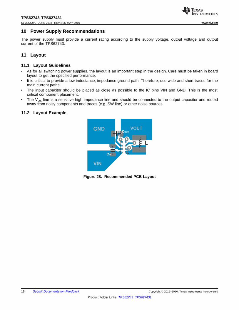
11.1 Layout Guidelines• As for all switching power supplies, the layout is an important step in the design. Care must be taken in board
layout to get the specified performance.• It is critical to provide a low inductance, impedance ground path. Therefore, use wide and short traces for the
main current paths.• The input capacitor should be placed as close as possible to the IC pins VIN and GND. This is the most
critical component placement.• The VOS line is a sensitive high impedance line and should be connected to the output capacitor and routed
away from noisy components and traces (e.g. SW line) or other noise sources.
11.2 Layout Example
Figure 28. Recommended PCB Layout
19
TPS62743, TPS627431www.ti.com SLVSCQ0A –JUNE 2015–REVISED MAY 2016
Product Folder Links: TPS62743 TPS627431
Submit Documentation FeedbackCopyright © 2015–2016, Texas Instruments Incorporated
12 Device and Documentation Support
12.1 Device Support
12.1.1 Third-Party Products DisclaimerTI'S PUBLICATION OF INFORMATION REGARDING THIRD-PARTY PRODUCTS OR SERVICES DOES NOTCONSTITUTE AN ENDORSEMENT REGARDING THE SUITABILITY OF SUCH PRODUCTS OR SERVICESOR A WARRANTY, REPRESENTATION OR ENDORSEMENT OF SUCH PRODUCTS OR SERVICES, EITHERALONE OR IN COMBINATION WITH ANY TI PRODUCT OR SERVICE.
12.2 Related LinksThe table below lists quick access links. Categories include technical documents, support and communityresources, tools and software, and quick access to sample or buy.
Table 6. Related Links
PARTS PRODUCT FOLDER SAMPLE & BUY TECHNICALDOCUMENTS
TOOLS &SOFTWARE
SUPPORT &COMMUNITY
TPS62743 Click here Click here Click here Click here Click hereTPS627431 Click here Click here Click here Click here Click here
12.3 Community ResourcesThe following links connect to TI community resources. Linked contents are provided "AS IS" by the respectivecontributors. They do not constitute TI specifications and do not necessarily reflect TI's views; see TI's Terms ofUse.
TI E2E™ Online Community TI's Engineer-to-Engineer (E2E) Community. Created to foster collaborationamong engineers. At e2e.ti.com, you can ask questions, share knowledge, explore ideas and helpsolve problems with fellow engineers.
Design Support TI's Design Support Quickly find helpful E2E forums along with design support tools andcontact information for technical support.
12.4 TrademarksDCS-Control, E2E are trademarks of Texas Instruments.Bluetooth is a registered trademark of Bluetooth SIG, Inc.All other trademarks are the property of their respective owners.
12.5 Electrostatic Discharge CautionThese devices have limited built-in ESD protection. The leads should be shorted together or the device placed in conductive foamduring storage or handling to prevent electrostatic damage to the MOS gates.
12.6 GlossarySLYZ022 — TI Glossary.
This glossary lists and explains terms, acronyms, and definitions.
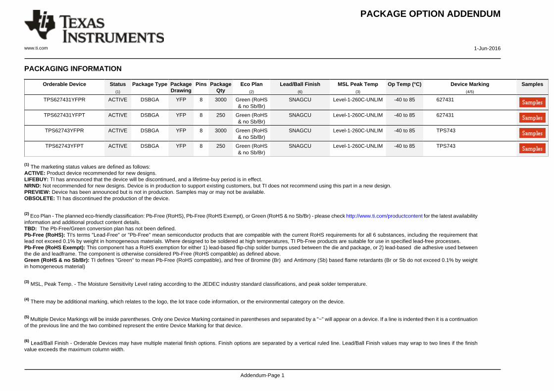
13 Mechanical, Packaging, and Orderable InformationThe following pages include mechanical, packaging, and orderable information. This information is the mostcurrent data available for the designated devices. This data is subject to change without notice and revision ofthis document. For browser-based versions of this data sheet, refer to the left-hand navigation.
PACKAGE OPTION ADDENDUM
www.ti.com 1-Jun-2016
Addendum-Page 1
PACKAGING INFORMATION
Orderable Device Status(1)
Package Type PackageDrawing
Pins PackageQty
Eco Plan(2)
Lead/Ball Finish(6)
MSL Peak Temp(3)
Op Temp (°C) Device Marking(4/5)
Samples
TPS627431YFPR ACTIVE DSBGA YFP 8 3000 Green (RoHS& no Sb/Br)
SNAGCU Level-1-260C-UNLIM -40 to 85 627431
TPS627431YFPT ACTIVE DSBGA YFP 8 250 Green (RoHS& no Sb/Br)
SNAGCU Level-1-260C-UNLIM -40 to 85 627431
TPS62743YFPR ACTIVE DSBGA YFP 8 3000 Green (RoHS& no Sb/Br)
SNAGCU Level-1-260C-UNLIM -40 to 85 TPS743
TPS62743YFPT ACTIVE DSBGA YFP 8 250 Green (RoHS& no Sb/Br)
SNAGCU Level-1-260C-UNLIM -40 to 85 TPS743
(1) The marketing status values are defined as follows:ACTIVE: Product device recommended for new designs.LIFEBUY: TI has announced that the device will be discontinued, and a lifetime-buy period is in effect.NRND: Not recommended for new designs. Device is in production to support existing customers, but TI does not recommend using this part in a new design.PREVIEW: Device has been announced but is not in production. Samples may or may not be available.OBSOLETE: TI has discontinued the production of the device.
(2) Eco Plan - The planned eco-friendly classification: Pb-Free (RoHS), Pb-Free (RoHS Exempt), or Green (RoHS & no Sb/Br) - please check http://www.ti.com/productcontent for the latest availabilityinformation and additional product content details.TBD: The Pb-Free/Green conversion plan has not been defined.Pb-Free (RoHS): TI's terms "Lead-Free" or "Pb-Free" mean semiconductor products that are compatible with the current RoHS requirements for all 6 substances, including the requirement thatlead not exceed 0.1% by weight in homogeneous materials. Where designed to be soldered at high temperatures, TI Pb-Free products are suitable for use in specified lead-free processes.Pb-Free (RoHS Exempt): This component has a RoHS exemption for either 1) lead-based flip-chip solder bumps used between the die and package, or 2) lead-based die adhesive used betweenthe die and leadframe. The component is otherwise considered Pb-Free (RoHS compatible) as defined above.Green (RoHS & no Sb/Br): TI defines "Green" to mean Pb-Free (RoHS compatible), and free of Bromine (Br) and Antimony (Sb) based flame retardants (Br or Sb do not exceed 0.1% by weightin homogeneous material)
(3) MSL, Peak Temp. - The Moisture Sensitivity Level rating according to the JEDEC industry standard classifications, and peak solder temperature.
(4) There may be additional marking, which relates to the logo, the lot trace code information, or the environmental category on the device.
(5) Multiple Device Markings will be inside parentheses. Only one Device Marking contained in parentheses and separated by a "~" will appear on a device. If a line is indented then it is a continuationof the previous line and the two combined represent the entire Device Marking for that device.
(6) Lead/Ball Finish - Orderable Devices may have multiple material finish options. Finish options are separated by a vertical ruled line. Lead/Ball Finish values may wrap to two lines if the finishvalue exceeds the maximum column width.
PACKAGE OPTION ADDENDUM
www.ti.com 1-Jun-2016
Addendum-Page 2
Important Information and Disclaimer:The information provided on this page represents TI's knowledge and belief as of the date that it is provided. TI bases its knowledge and belief on informationprovided by third parties, and makes no representation or warranty as to the accuracy of such information. Efforts are underway to better integrate information from third parties. TI has taken andcontinues to take reasonable steps to provide representative and accurate information but may not have conducted destructive testing or chemical analysis on incoming materials and chemicals.TI and TI suppliers consider certain information to be proprietary, and thus CAS numbers and other limited information may not be available for release.
In no event shall TI's liability arising out of such information exceed the total purchase price of the TI part(s) at issue in this document sold by TI to Customer on an annual basis.
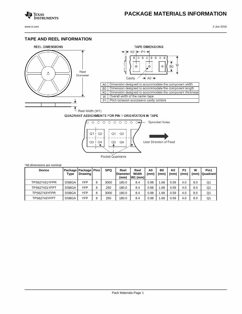
TAPE AND REEL INFORMATION
*All dimensions are nominal
Device PackageType
PackageDrawing
Pins SPQ ReelDiameter
(mm)
ReelWidth
W1 (mm)
A0(mm)
B0(mm)
K0(mm)
P1(mm)
W(mm)
Pin1Quadrant
TPS627431YFPR DSBGA YFP 8 3000 180.0 8.4 0.98 1.68 0.59 4.0 8.0 Q1
TPS627431YFPT DSBGA YFP 8 250 180.0 8.4 0.98 1.68 0.59 4.0 8.0 Q1
TPS62743YFPR DSBGA YFP 8 3000 180.0 8.4 0.98 1.68 0.59 4.0 8.0 Q1
TPS62743YFPT DSBGA YFP 8 250 180.0 8.4 0.98 1.68 0.59 4.0 8.0 Q1
PACKAGE MATERIALS INFORMATION
www.ti.com 2-Jun-2016
Pack Materials-Page 1
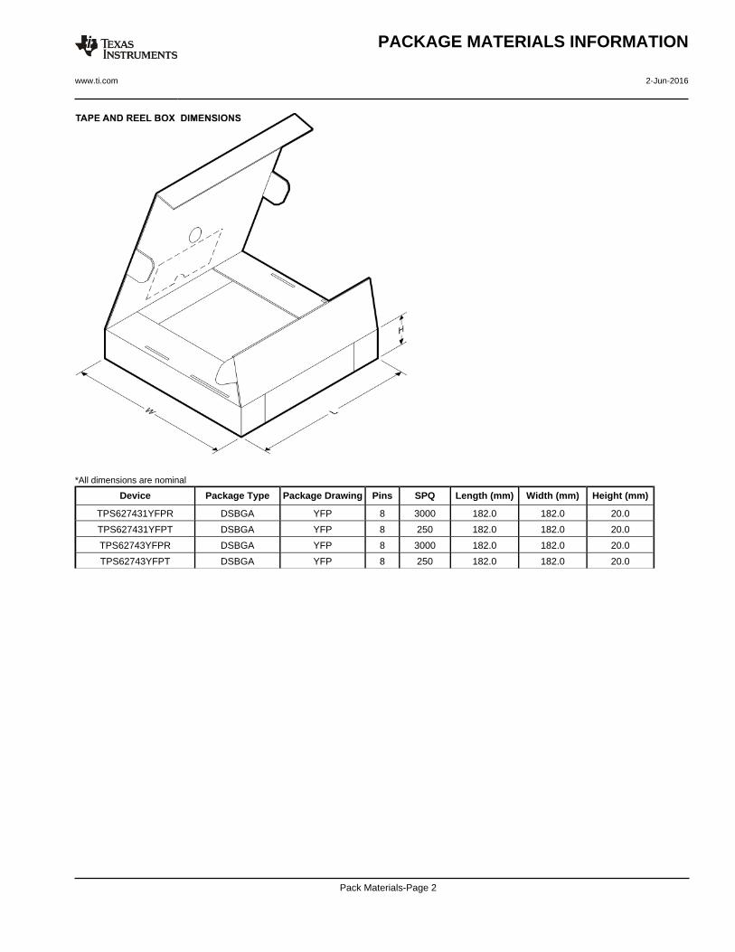
*All dimensions are nominal
Device Package Type Package Drawing Pins SPQ Length (mm) Width (mm) Height (mm)
TPS627431YFPR DSBGA YFP 8 3000 182.0 182.0 20.0
TPS627431YFPT DSBGA YFP 8 250 182.0 182.0 20.0
TPS62743YFPR DSBGA YFP 8 3000 182.0 182.0 20.0
TPS62743YFPT DSBGA YFP 8 250 182.0 182.0 20.0
PACKAGE MATERIALS INFORMATION
www.ti.com 2-Jun-2016
Pack Materials-Page 2
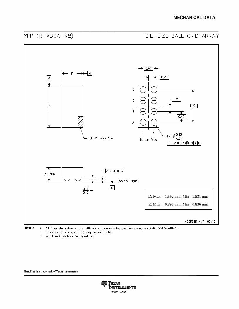
D: Max =
E: Max =
1.592 mm, Min =
0.896 mm, Min =
1.531 mm
0.836 mm
IMPORTANT NOTICE
Texas Instruments Incorporated (TI) reserves the right to make corrections, enhancements, improvements and other changes to itssemiconductor products and services per JESD46, latest issue, and to discontinue any product or service per JESD48, latest issue. Buyersshould obtain the latest relevant information before placing orders and should verify that such information is current and complete.TI’s published terms of sale for semiconductor products (http://www.ti.com/sc/docs/stdterms.htm) apply to the sale of packaged integratedcircuit products that TI has qualified and released to market. Additional terms may apply to the use or sale of other types of TI products andservices.Reproduction of significant portions of TI information in TI data sheets is permissible only if reproduction is without alteration and isaccompanied by all associated warranties, conditions, limitations, and notices. TI is not responsible or liable for such reproduceddocumentation. Information of third parties may be subject to additional restrictions. Resale of TI products or services with statementsdifferent from or beyond the parameters stated by TI for that product or service voids all express and any implied warranties for theassociated TI product or service and is an unfair and deceptive business practice. TI is not responsible or liable for any such statements.Buyers and others who are developing systems that incorporate TI products (collectively, “Designers”) understand and agree that Designersremain responsible for using their independent analysis, evaluation and judgment in designing their applications and that Designers havefull and exclusive responsibility to assure the safety of Designers' applications and compliance of their applications (and of all TI productsused in or for Designers’ applications) with all applicable regulations, laws and other applicable requirements. Designer represents that, withrespect to their applications, Designer has all the necessary expertise to create and implement safeguards that (1) anticipate dangerousconsequences of failures, (2) monitor failures and their consequences, and (3) lessen the likelihood of failures that might cause harm andtake appropriate actions. Designer agrees that prior to using or distributing any applications that include TI products, Designer willthoroughly test such applications and the functionality of such TI products as used in such applications.TI’s provision of technical, application or other design advice, quality characterization, reliability data or other services or information,including, but not limited to, reference designs and materials relating to evaluation modules, (collectively, “TI Resources”) are intended toassist designers who are developing applications that incorporate TI products; by downloading, accessing or using TI Resources in anyway, Designer (individually or, if Designer is acting on behalf of a company, Designer’s company) agrees to use any particular TI Resourcesolely for this purpose and subject to the terms of this Notice.TI’s provision of TI Resources does not expand or otherwise alter TI’s applicable published warranties or warranty disclaimers for TIproducts, and no additional obligations or liabilities arise from TI providing such TI Resources. TI reserves the right to make corrections,enhancements, improvements and other changes to its TI Resources. TI has not conducted any testing other than that specificallydescribed in the published documentation for a particular TI Resource.Designer is authorized to use, copy and modify any individual TI Resource only in connection with the development of applications thatinclude the TI product(s) identified in such TI Resource. NO OTHER LICENSE, EXPRESS OR IMPLIED, BY ESTOPPEL OR OTHERWISETO ANY OTHER TI INTELLECTUAL PROPERTY RIGHT, AND NO LICENSE TO ANY TECHNOLOGY OR INTELLECTUAL PROPERTYRIGHT OF TI OR ANY THIRD PARTY IS GRANTED HEREIN, including but not limited to any patent right, copyright, mask work right, orother intellectual property right relating to any combination, machine, or process in which TI products or services are used. Informationregarding or referencing third-party products or services does not constitute a license to use such products or services, or a warranty orendorsement thereof. Use of TI Resources may require a license from a third party under the patents or other intellectual property of thethird party, or a license from TI under the patents or other intellectual property of TI.TI RESOURCES ARE PROVIDED “AS IS” AND WITH ALL FAULTS. TI DISCLAIMS ALL OTHER WARRANTIES ORREPRESENTATIONS, EXPRESS OR IMPLIED, REGARDING RESOURCES OR USE THEREOF, INCLUDING BUT NOT LIMITED TOACCURACY OR COMPLETENESS, TITLE, ANY EPIDEMIC FAILURE WARRANTY AND ANY IMPLIED WARRANTIES OFMERCHANTABILITY, FITNESS FOR A PARTICULAR PURPOSE, AND NON-INFRINGEMENT OF ANY THIRD PARTY INTELLECTUALPROPERTY RIGHTS. TI SHALL NOT BE LIABLE FOR AND SHALL NOT DEFEND OR INDEMNIFY DESIGNER AGAINST ANY CLAIM,INCLUDING BUT NOT LIMITED TO ANY INFRINGEMENT CLAIM THAT RELATES TO OR IS BASED ON ANY COMBINATION OFPRODUCTS EVEN IF DESCRIBED IN TI RESOURCES OR OTHERWISE. IN NO EVENT SHALL TI BE LIABLE FOR ANY ACTUAL,DIRECT, SPECIAL, COLLATERAL, INDIRECT, PUNITIVE, INCIDENTAL, CONSEQUENTIAL OR EXEMPLARY DAMAGES INCONNECTION WITH OR ARISING OUT OF TI RESOURCES OR USE THEREOF, AND REGARDLESS OF WHETHER TI HAS BEENADVISED OF THE POSSIBILITY OF SUCH DAMAGES.Unless TI has explicitly designated an individual product as meeting the requirements of a particular industry standard (e.g., ISO/TS 16949and ISO 26262), TI is not responsible for any failure to meet such industry standard requirements.Where TI specifically promotes products as facilitating functional safety or as compliant with industry functional safety standards, suchproducts are intended to help enable customers to design and create their own applications that meet applicable functional safety standardsand requirements. Using products in an application does not by itself establish any safety features in the application. Designers mustensure compliance with safety-related requirements and standards applicable to their applications. Designer may not use any TI products inlife-critical medical equipment unless authorized officers of the parties have executed a special contract specifically governing such use.Life-critical medical equipment is medical equipment where failure of such equipment would cause serious bodily injury or death (e.g., lifesupport, pacemakers, defibrillators, heart pumps, neurostimulators, and implantables). Such equipment includes, without limitation, allmedical devices identified by the U.S. Food and Drug Administration as Class III devices and equivalent classifications outside the U.S.TI may expressly designate certain products as completing a particular qualification (e.g., Q100, Military Grade, or Enhanced Product).Designers agree that it has the necessary expertise to select the product with the appropriate qualification designation for their applicationsand that proper product selection is at Designers’ own risk. Designers are solely responsible for compliance with all legal and regulatoryrequirements in connection with such selection.Designer will fully indemnify TI and its representatives against any damages, costs, losses, and/or liabilities arising out of Designer’s non-compliance with the terms and provisions of this Notice.
Mailing Address: Texas Instruments, Post Office Box 655303, Dallas, Texas 75265Copyright © 2017, Texas Instruments Incorporated