Embed Size (px)
Citation preview
Tracker Upgrade Week –Sensors Meeting
Sensor Production
24. July 2014
Marko Dragicevic
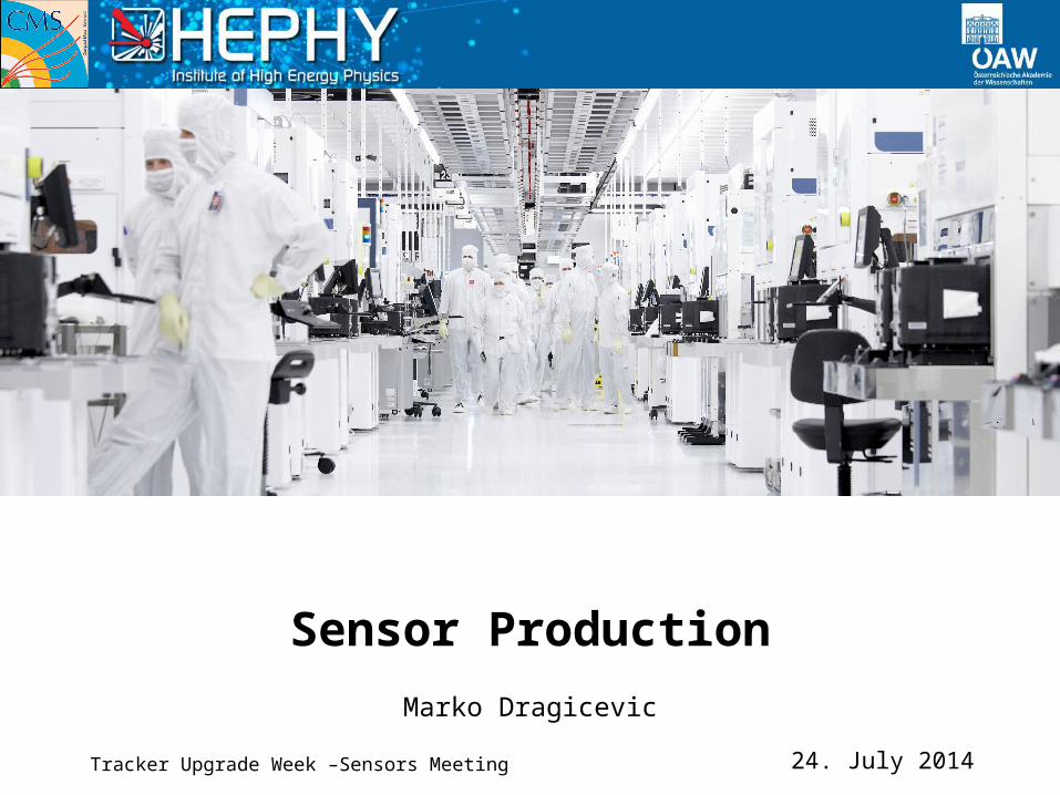
MAPSA LIGHT SENSOR
Marko Dragicevic24. July 2014 2
Status
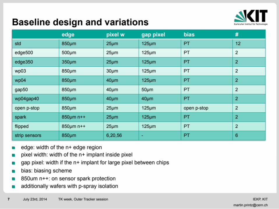
• Design of sensors and all its variations is ready!– Kudos to Martin Printz (KIT)– An internal design review was conducted between sensor and electronics
group– Made sure that interface between sensor and chip (location of bump bonds)
is correct
• A wafer layout has been proposed – Already contains plenty of sensors for all envisaged assembly and sensor
studies– There would still be some space left…– Otherwise it will be populated with more copies of the existing structures– Deadline: 1. August 2014
• Order from procurement office to CiS is already out– CiS is waiting for the final GDS– Costs for 14 wafers: 27 kEUR (33 kCHF)
Marko Dragicevic24. July 2014
MaPSA light
3

4Marko Dragicevic24. July 2014
5Marko Dragicevic24. July 2014
6Marko Dragicevic24. July 2014
7Marko Dragicevic24. July 2014
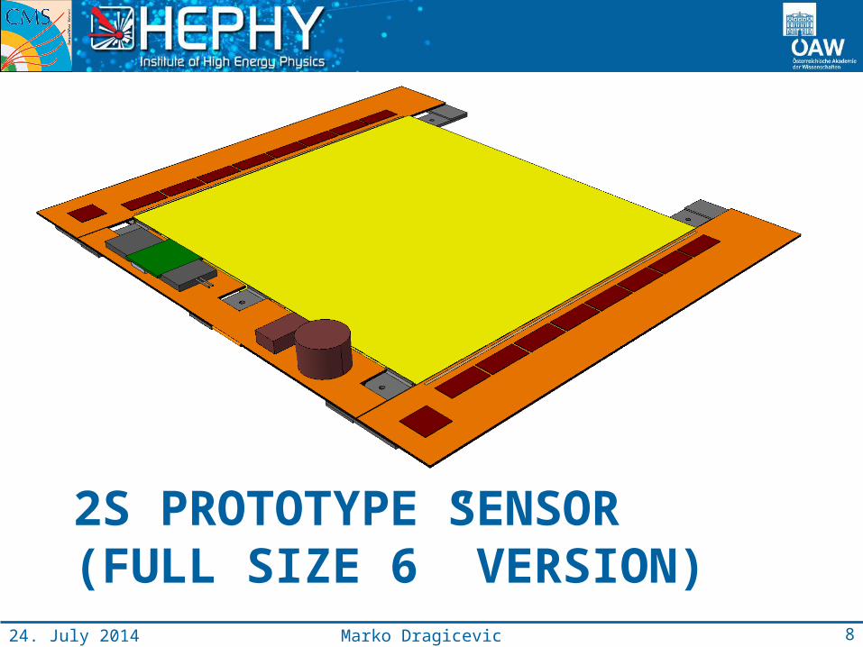
2S PROTOTYPE SENSOR(FULL SIZE 6” VERSION)
Marko Dragicevic24. July 2014 8
Status
• Sensor group is working on– Sensor design and wafer layout– Definition of materials and process options– Expected to be ready be the end of summer
• Start administrative process with CERN procurement now– We need to decide were we want to buy and how
much
9Marko Dragicevic24. July 2014
2S Prototype
Production: Costs
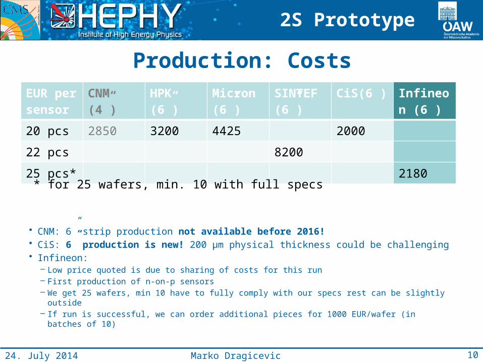
• CNM: 6” strip production not available before 2016!• CiS: 6” production is new! 200 µm physical thickness could be challenging• Infineon:
– Low price quoted is due to sharing of costs for this run– First production of n-on-p sensors– We get 25 wafers, min 10 have to fully comply with our specs rest can be slightly outside– If run is successful, we can order additional pieces for 1000 EUR/wafer (in batches of 10)
Marko Dragicevic24. July 2014
EUR per sensor
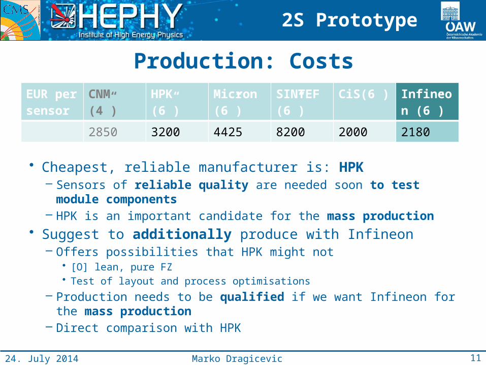
CNM (4”) HPK (6”) Micron (6”)
SINTEF (6”)
CiS(6”) Infineon (6”)
20 pcs 2850 3200 4425 2000
22 pcs 8200
25 pcs* 2180
* for 25 wafers, min. 10 with full specs
2S Prototype
10
Production: Costs
• Cheapest, reliable manufacturer is: HPK– Sensors of reliable quality are needed soon to test module
components– HPK is an important candidate for the mass production
• Suggest to additionally produce with Infineon – Offers possibilities that HPK might not
• [O] lean, pure FZ• Test of layout and process optimisations
– Production needs to be qualified if we want Infineon for the mass production
– Direct comparison with HPK
11Marko Dragicevic24. July 2014
EUR per sensor
CNM (4”) HPK (6”) Micron (6”)
SINTEF (6”)
CiS(6”) Infineon (6”)
2850 3200 4425 8200 2000 2180
2S Prototype
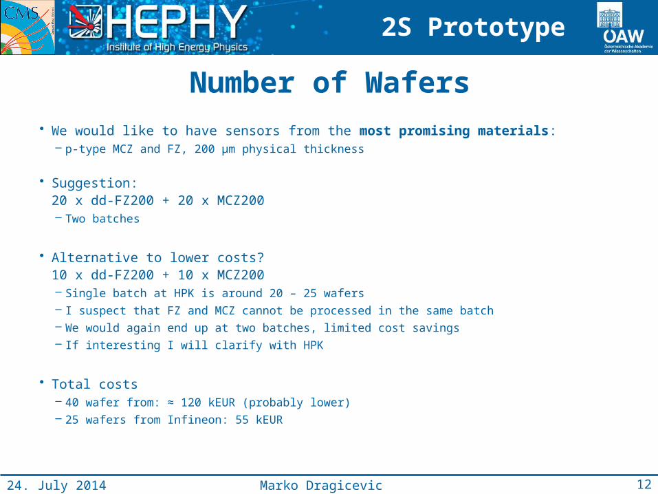
• We would like to have sensors from the most promising materials:– p-type MCZ and FZ, 200 µm physical thickness
• Suggestion:20 x dd-FZ200 + 20 x MCZ200– Two batches
• Alternative to lower costs?10 x dd-FZ200 + 10 x MCZ200– Single batch at HPK is around 20 – 25 wafers– I suspect that FZ and MCZ cannot be processed in the same batch– We would again end up at two batches, limited cost savings– If interesting I will clarify with HPK
• Total costs – 40 wafer from: ≈ 120 kEUR (probably lower)– 25 wafers from Infineon: 55 kEUR
Number of Wafers
12Marko Dragicevic24. July 2014
2S Prototype
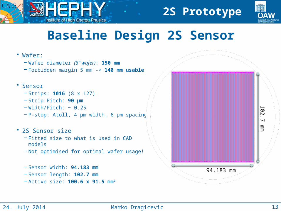
Baseline Design 2S Sensor• Wafer:
– Wafer diameter (6” wafer): 150 mm– Forbidden margin 5 mm -> 140 mm usable
• Sensor– Strips: 1016 (8 x 127)– Strip Pitch: 90 µm– Width/Pitch: ~ 0.25– P-stop: Atoll, 4 µm width, 6 µm spacing
• 2S Sensor size
– Fitted size to what is used in CAD models– Not optimised for optimal wafer usage!
– Sensor width: 94.183 mm– Sensor length: 102.7 mm– Active size: 100.6 x 91.5 mm2
Marko Dragicevic24. July 2014
150 mm
5 mm
140
mm
2S Prototype
13
94.183 mm
102.7 m
m
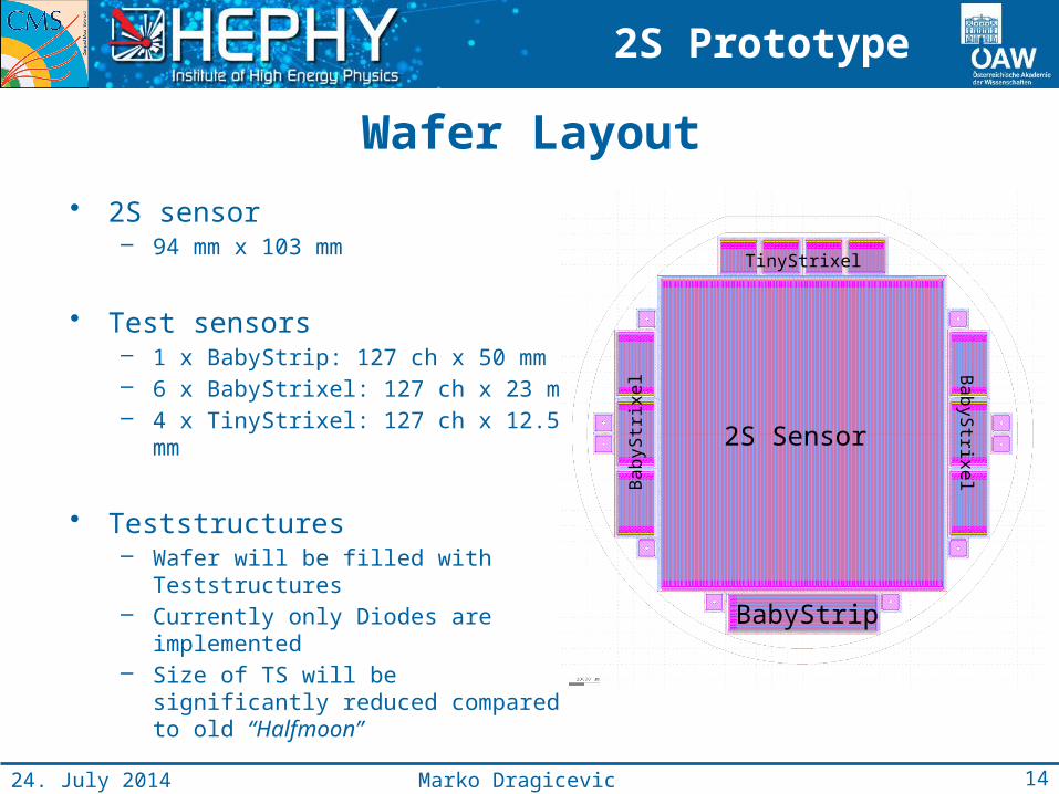
Wafer Layout
Marko Dragicevic24. July 2014
• 2S sensor– 94 mm x 103 mm
• Test sensors– 1 x BabyStrip: 127 ch x 50 mm – 6 x BabyStrixel: 127 ch x 23 mm– 4 x TinyStrixel: 127 ch x 12.5 mm
• Teststructures– Wafer will be filled with Teststructures– Currently only Diodes are implemented– Size of TS will be significantly reduced
compared to old “Halfmoon”
2S Prototype
14
2S Sensor
BabyStripB
ab
yStr
ixe
l Ba
byS
trixel
TinyStrixel
2S Sensor
BabyStripB
ab
yStr
ixe
l Ba
byS
trixel
TinyStrixel
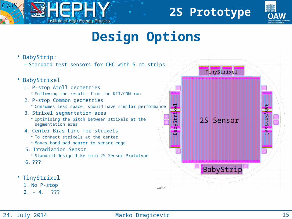
Design Options• BabyStrip:
– Standard test sensors for CBC with 5 cm strips
• BabyStrixel1. P-stop Atoll geometries
• Following the results from the KIT/CNM run
2. P-stop Common geometries• Consumes less space, should have similar performance
3. Strixel segmentation area• Optimising the pitch between strixels at the segmentation
area
4. Center Bias Line for strixels• To connect strixels at the center• Moves bond pad nearer to sensor edge
5. Irradiation Sensor• Standard design like main 2S Sensor Prototype
6. ???
• TinyStrixel1. No P-stop
2. - 4. ???
15Marko Dragicevic24. July 2014
2S Prototype
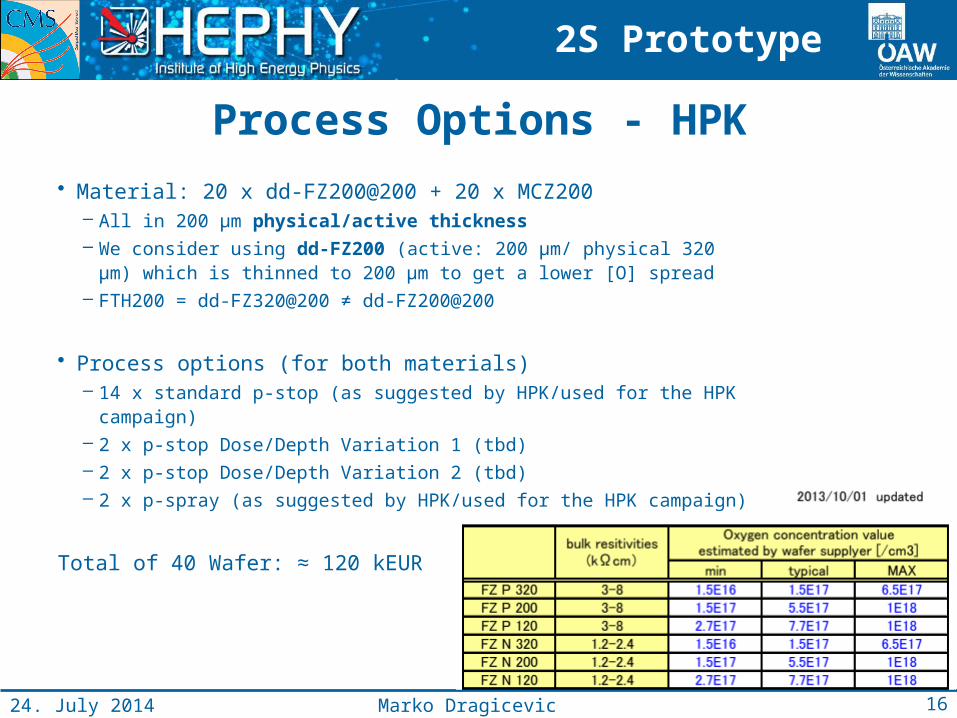
• Material: 20 x dd-FZ200@200 + 20 x MCZ200– All in 200 µm physical/active thickness– We consider using dd-FZ200 (active: 200 µm/ physical 320 µm)
which is thinned to 200 µm to get a lower [O] spread– FTH200 = dd-FZ320@200 ≠ dd-FZ200@200
• Process options (for both materials) – 14 x standard p-stop (as suggested by HPK/used for the HPK
campaign)– 2 x p-stop Dose/Depth Variation 1 (tbd)– 2 x p-stop Dose/Depth Variation 2 (tbd)– 2 x p-spray (as suggested by HPK/used for the HPK campaign)
Total of 40 Wafer: ≈ 120 kEUR
Process Options - HPK
16Marko Dragicevic24. July 2014
2S Prototype
Process Options - Infineon
• Material: 20 x FZ200+ 5 x MCZ200– All in 200 µm physical/active thickness– The FZ material is pure oxygen lean ([O] < 2E16/cm3) FZ
• Process options– First production of NonP sensors at Infineon– Need to tune parameters for all implantations, especially p-stop
and p-spray– Will discuss with Infineon
Total of 25 Wafer: = 55 kEUR
(Then 10 kEUR/10 wafers with same masks)17Marko Dragicevic24. July 2014
2S Prototype
Tentative Timeline
• Until September (CMS Upgrade Week)– Finalize sensor design and wafer layout– Define materials and process– Start administrative process with CERN
Procurement (HPK and Infineon)
• September – Beginning 2015– Start the production– HPK: Approximate lead time is 4 months,
procurement of wafers might add some time– Infineon: potentially faster, but many unknowns
18Marko Dragicevic24. July 2014
2S Prototype
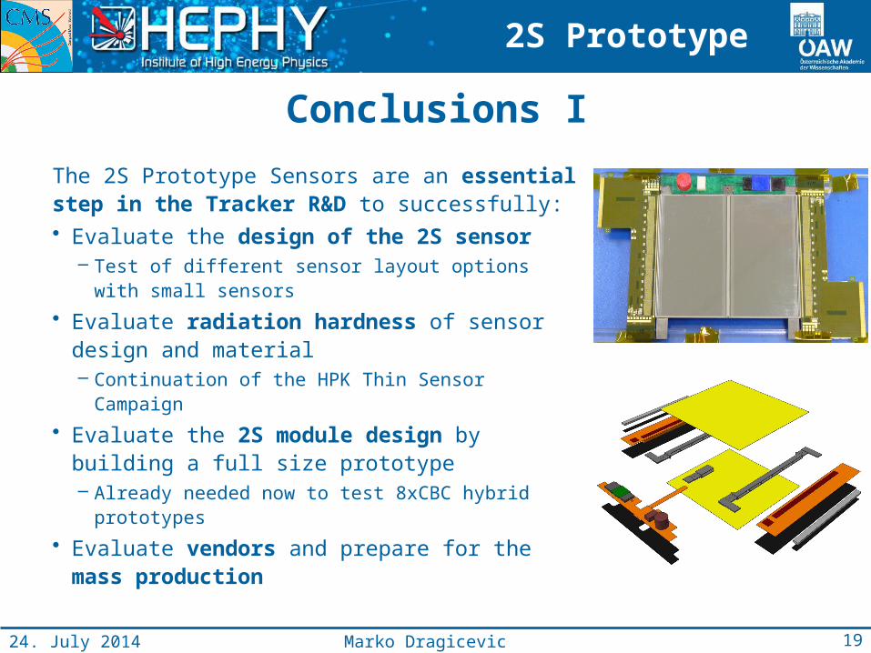
Conclusions I
The 2S Prototype Sensors are an essential step in the Tracker R&D to successfully:• Evaluate the design of the 2S sensor
– Test of different sensor layout options with small sensors
• Evaluate radiation hardness of sensor design and material– Continuation of the HPK Thin Sensor Campaign
• Evaluate the 2S module design by building a full size prototype– Already needed now to test 8xCBC hybrid
prototypes
• Evaluate vendors and prepare for the mass production
19Marko Dragicevic24. July 2014
2S Prototype
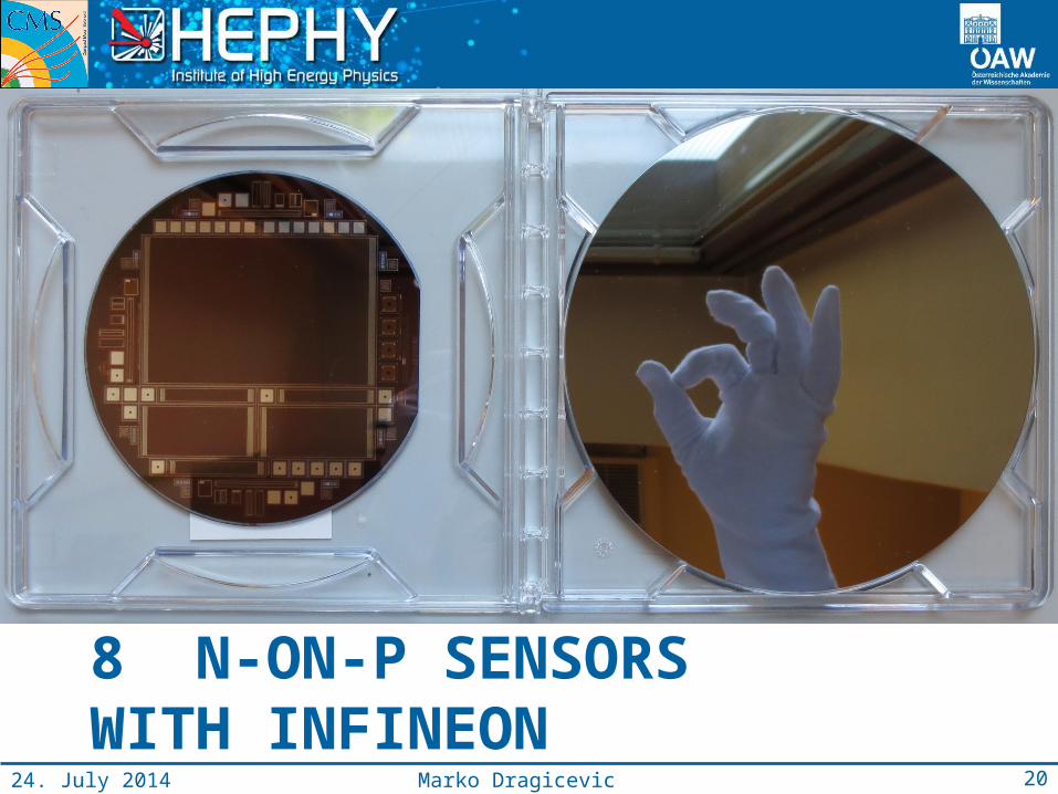
8” N-ON-P SENSORSWITH INFINEON
Marko Dragicevic24. July 2014 20
Status
• Order is already out for some time– To encourage Infineon to work on it
• Costs: 120 kEUR• Sensor design and layout will be inherited from the 6” 2S Sensor
Prototype Run• Infineon has defined the process plan• They have processed one batch of 8” wafers going through the
complete process with arbitrary masks (Kurzläufer)• Goal:
Estimate the yield for a 8” production at 200 µm thickness
Outcome:
All wafers survived!21Marko Dragicevic24. July 2014
8” Infineon
Conclusions II
22Marko Dragicevic24. July 2014
Upcoming sensors productions (2S, MAPSA-light and 8”) will yield plenty of test sensors and structures!
Great opportunity to:• Join the effort to characterise sensors and
test structure• To perform interesting studies with your
students
If you are interested contact• Alexander Dierlamm• Marko Dragicevic
THANKS FOR YOUR ATTENTION!