Embed Size (px)
Citation preview

Pages 1 to 16
Document Custodian: European Space Agency - see https://escies.org
TRANSISTORS, LOW POWER, PNP
BASED ON TYPE 2N2894 and 2N2894A
ESCC Detail Specification No. 5202/004
Issue 2 January 2009
ESCC Detail Specification No. 5202/004PAGE 2
ISSUE 2
LEGAL DISCLAIMER AND COPYRIGHT
European Space Agency, Copyright © 2009. All rights reserved.
The European Space Agency disclaims any liability or responsibility, to any person or entity, with respectto any loss or damage caused, or alleged to be caused, directly or indirectly by the use and applicationof this ESCC publication.
This publication, without the prior permission of the European Space Agency and provided that it is notused for a commercial purpose, may be:
– copied in whole, in any medium, without alteration or modification.– copied in part, in any medium, provided that the ESCC document identification, comprising the
ESCC symbol, document number and document issue, is removed.

ESCC Detail Specification No. 5202/004PAGE 3
ISSUE 2
DOCUMENTATION CHANGE NOTICE
(Refer to https://escies.org for ESCC DCR content)
DCR No. CHANGE DESCRIPTION
442 Specification up issued to incorporate editorial and technical changes per DCR.

ESCC Detail Specification No. 5202/004PAGE 4
ISSUE 2
TABLE OF CONTENTS
1. GENERAL 5
1.1 Scope 51.2 Applicable Documents 51.3 Terms, Definitions, Abbreviations, Symbols and Units 51.4 The ESCC Component Number and Component Type Variants 51.4.1 The ESCC Component Number 51.4.2 Component Type Variants 51.5 Maximum Ratings 61.6 Physical Dimensions and Terminal Identification 71.6.1 Metal Can Package (TO-18) - 3 lead 71.6.2 Chip Carrier Package (CCP) - 3 terminal 81.7 Functional Diagram 91.8 Materials and Finishes 9
2. REQUIREMENTS 9
2.1 General 92.1.1 Deviations from the Generic Specification 92.2 Marking 102.3 Terminal Strength 102.4 Electrical Measurements at Room, High and Low Temperatures 102.4.1 Room Temperature Electrical Measurements 102.4.2 High and Low Temperatures Electrical Measurements 152.5 Parameter Drift Values 152.6 Intermediate and End-Point Electrical Measurements 152.7 High Temperature Reverse Bias Burn-in Conditions 162.8 Power Burn-in Conditions 162.9 Operating Life Conditions 16

ESCC Detail Specification No. 5202/004PAGE 5
ISSUE 2
1. GENERAL
1.1 SCOPEThis specification details the ratings, physical and electrical characteristics and test and inspection datafor the component type variants and/or the range of components specified below. It supplements therequirements of, and shall be read in conjunction with, the ESCC Generic Specification listed underApplicable Documents.
1.2 APPLICABLE DOCUMENTSThe following documents form part of this specification and shall be read in conjunction with it:
(a) ESCC Generic Specification No. 5000(b) MIL-STD-750, Test Methods and Procedures for Semiconductor Devices
1.3 TERMS, DEFINITIONS, ABBREVIATIONS, SYMBOLS AND UNITSFor the purpose of this specification, the terms, definitions, abbreviations, symbols and units specified inESCC Basic Specification No. 21300 shall apply.
1.4 THE ESCC COMPONENT NUMBER AND COMPONENT TYPE VARIANTS
1.4.1 The ESCC Component Number
The ESCC Component Number shall be constituted as follows:
Example: 520200401
• Detail Specification Reference: 5202004• Component Type Variant Number: 01 (as required)
1.4.2 Component Type Variants
The component type variants applicable to this specification are as follows:
The lead/terminal material and/or finish shall be in accordance with the requirements of ESCC BasicSpecification No. 23500.
VariantNumber
Based on Type Case Lead/Terminal Materialand/or Finish
Weightmax g
01 2N2894 TO-18 D2 0.4
02 2N2894 TO-18 D2 0.4
03 2N2894 TO-18 D3 or D4 0.4
04 2N2894 TO-18 D3 or D4 0.4
05 2N2894 TO-18 D7 0.4
06 2N2894 CCP 2 0.06
07 2N2894 CCP 4 0.06

ESCC Detail Specification No. 5202/004PAGE 6
ISSUE 2
1.5 MAXIMUM RATINGSThe maximum ratings shall not be exceeded at any time during use or storage.
Maximum ratings shall only be exceeded during testing to the extent specified in this specification andwhen stipulated in Test Methods and Procedures of the ESCC Generic Specification.
NOTES:1. For Tamb or Tcase > +25oC, derate linearly to 0W at +200oC.2. When mounted on a 15 x 15 x 0.6mm ceramic substrate.3. For Variants with tin-lead plating or hot solder dip lead finish all testing, and any handling, performed
at Tamb > +125oC shall be carried out in a 100% inert atmosphere.4. Duration 10 seconds maximum at a distance of not less than 1.5mm from the device body and the
same lead shall not be resoldered until 3 minutes have elapsed.5. Duration 5 seconds maximum and the same terminal shall not be resoldered until 3 minutes have
elapsed.
Characteristics Symbols Maximum Ratings Unit Remarks
Collector-Base Voltage VCBO -12 V Over entireoperating
temperaturerange
Collector-Emitter Voltage VCEO -12 V
Emitter-Base Voltage VEBO -4 V
Collector Current IC -200 mA Continuous
Power DissipationFor TO-18 and CCP Ptot1 0.36 W
At Tamb ≤ +25oCNote 1
For CCP Ptot2 0.58 (Note 2) W
For TO-18 Ptot3 1.2 W At Tcase ≤ +25oCNote 1
Operating Temperature Range Top -65 to +200 oC Note 3
Storage Temperature Range Tstg -65 to +200 oC Note 3
Soldering TemperatureFor TO-18For CCP
Tsol+260+245
oCNote 4Note 5

ESCC Detail Specification No. 5202/004PAGE 7
ISSUE 2
1.6 PHYSICAL DIMENSIONS AND TERMINAL IDENTIFICATION
1.6.1 Metal Can Package (TO-18) - 3 lead
NOTES:1. Terminal identification is specified by reference to the tab position where lead 1 = emitter, lead 2 =
base, lead 3 = collector.2. Applies to all leads.3. Øb2 applies between L1 and L2. Øb applies between L2 and 12.7mm from the seating plane.
Diameter is uncontrolled within L1 and beyond 12.7mm from the seating plane.4. Leads having maximum diameter 0.483mm measured in the gauging plane 1.37(+0.025,-0)mm
SymbolsDimensions mm
NotesMin Max
A 4.32 5.33
Øb 0.406 0.533 2, 3
Øb2 0.406 0.483 2, 3
ØD 5.31 5.84
ØD1 4.52 4.95
e 2.54 BSC 4
e1 1.27 BSC 4
F - 0.762
j 0.914 1.17
k 0.711 1.22 5
L 12.7 - 2
L1 - 1.27 3
L2 6.35 - 3
a 45o BSC 1, 4, 6
L1
F
k1
2
3
∅b
∅D1
LA
∅D
a
e
j
L2
∅b2
e1
e1
Seating plane
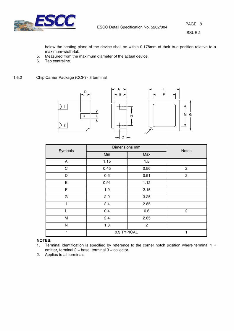
ESCC Detail Specification No. 5202/004PAGE 8
ISSUE 2
below the seating plane of the device shall be within 0.178mm of their true position relative to amaximum-width-tab.
5. Measured from the maximum diameter of the actual device.6. Tab centreline.
1.6.2 Chip Carrier Package (CCP) - 3 terminal
NOTES:1. Terminal identification is specified by reference to the corner notch position where terminal 1 =
emitter, terminal 2 = base, terminal 3 = collector.2. Applies to all terminals.
SymbolsDimensions mm
NotesMin Max
A 1.15 1.5
C 0.45 0.56 2
D 0.6 0.91 2
E 0.91 1.12
F 1.9 2.15
G 2.9 3.25
I 2.4 2.85
L 0.4 0.6 2
M 2.4 2.65
N 1.8 2
r 0.3 TYPICAL 1
L
D
1
3
2
N
E
A
Cr
M G
I
F

ESCC Detail Specification No. 5202/004PAGE 9
ISSUE 2
1.7 FUNCTIONAL DIAGRAM
NOTES:1. For TO-18, the collector is internally connected to the case.2. For CCP, the lid is not connected to any terminal.
1.8 MATERIALS AND FINISHESMaterials and finishes shall be as follows:
a) CaseFor the metal can package the case shall be hermetically sealed and have a metal body with hardglass seals.
For the chip carrier package the case shall be hermetically sealed and have a ceramic body with aKovar lid.
b) Leads/TerminalsAs specified in Component Type Variants.
2. REQUIREMENTS
2.1 GENERALThe complete requirements for procurement of the components specified herein are as stated in thisspecification and the ESCC Generic Specification. Permitted deviations from the Generic Specification,applicable to this specification only, are listed below.
Permitted deviations from the Generic Specification and this Detail Specification, formally agreed withspecific Manufacturers on the basis that the alternative requirements are equivalent to the ESCCrequirement and do not affect the component’s reliability, are listed in the appendices attached to thisspecification.
2.1.1 Deviations from the Generic Specification
None.
3
2
1
1. Emitter2. Base.3. Collector

ESCC Detail Specification No. 5202/004PAGE 10
ISSUE 2
2.2 MARKINGThe marking shall be in accordance with the requirements of ESCC Basic Specification No. 21700 andas follows.
The information to be marked on the component shall be:
(a) The ESCC qualified components symbol (for ESCC qualified components only).(b) The ESCC Component Number.(c) Traceability information.
2.3 TERMINAL STRENGTHThe test conditions for terminal strength, tested as specified in the ESCC Generic Specification, shall beas follows:
For TO-18, Test Condition: E, lead fatigue.
2.4 ELECTRICAL MEASUREMENTS AT ROOM, HIGH AND LOW TEMPERATURESElectrical measurements shall be performed at room, high and low temperatures.
2.4.1 Room Temperature Electrical Measurements
The measurements shall be performed at Tamb=+22 ±3oC.

ESCC Detail Specification No. 5202/004PAGE 11
ISSUE 2
Characteristics Symbols MIL-STD-750Test Method
Test Conditions Limits Units
Min Max
Collector-EmitterBreakdownVoltage
V(BR)CEO 3011 IC = -10mANote 1Bias condition D
-12 - V
Collector-BaseBreakdownVoltage
V(BR)CBO 3001 IC = -10μABias condition D
-12 - V
Emitter-BaseBreakdownVoltage
V(BR)EBO 3026 IE = -100μABias condition D
-4 - V
Collector-BaseCut-off Current
ICBO 3036 VCB= -10VBias condition D
- -100 nA
Forward-CurrentTransfer Ratio
hFE1 3076 VCE=-300mV;IC=-10mANote 12N28942N2894A
30-
--
-
hFE2 3076 VCE=-500mV;IC=-30mANote 12N28942N2894A
4040
150120
-
hFE3 3076 VCE=-1V;IC=-100mANote 12N28942N2894A
2530
--
-
Collector-EmitterSaturation Voltage
VCE(sat)1 3071 IC=-10mAIB=-1mANote 12N28942N2894A
--
-150-
mV
VCE(sat)2 3071 IC=-30mAIB=-3mANote 12N28942N2894A
--
-200-190
mV
VCE(sat)3 3071 IC=-100mAIB=-10mANote 12N28942N2894A
--
-500-450
mV

ESCC Detail Specification No. 5202/004PAGE 12
ISSUE 2
NOTES:1. Pulse measurement: Pulse Width ≤ 300μs, Duty Cycle ≤ 2%2. For AC characteristics read and record measurements shall be performed on a sample of 32
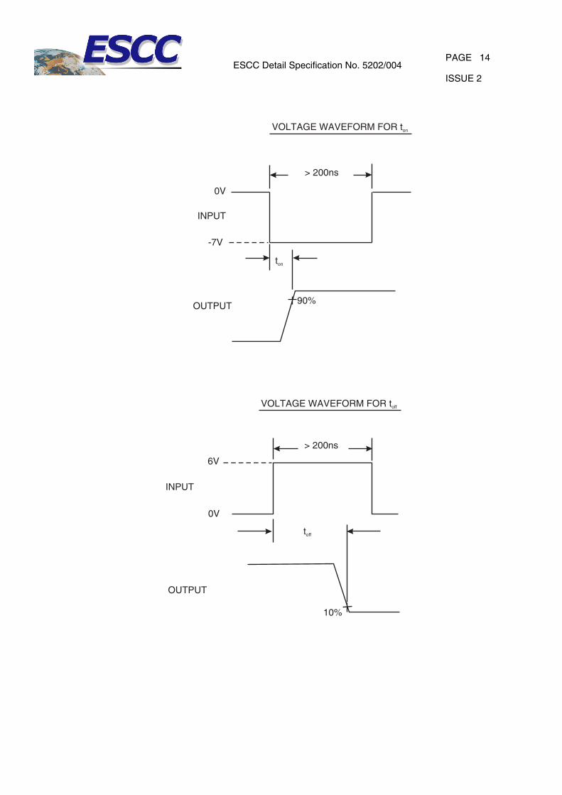
components with 0 failures allowed. Alternatively a 100% inspection may be performed.3. ton shall be measured using the following test circuit. The input waveform shall be supplied by a
pulse generator with the following characteristics: ZOUT = 50Ω, tr ≤ 2ns, Pulse Width = 200 ±10ns,Duty Cycle ≤ 2%. The output waveform shall be monitored on an oscilloscope with the following
Base-EmitterSaturation Voltage
VBE(sat)1 3066 IC=-10mAIB=-1mANote 1Test condition A2N28942N2894A
-780-
-980-
mV
VBE(sat)2 3066 IC=-30mAIB=-3mANote 1Test condition A2N28942N2894A
-0.85-
-1.2-1.15
V
Magnitude ofSmall-SignalShort-CircuitForward-CurrentTransfer Ratio
|hfe| 3306 VCB=-30mA,VCE=-10Vf=100MHzNote 22N29842N2894A
47
--
-
OutputCapacitance
Cobo 3236 VCB=-5V,IE=0Af=1MHzNote 22N29842N2894A
--
64.5
pF
Input Capacitance Cibo 3240 VEB=-500mVIC=0Af=1MHzNote 2
- 6 pF
Turn-on Time ton - VBB=3V, VIN=-7V,IC=-30mAIBL=1.5mANotes 2, 32N29842N2894A
--
6040
ns
Turn-off Time toff - VBB=-4V, VIN=6V,IC=-30mAIB1=IB2=1.5mANotes 2, 32N29842N2894A
--
9060
ns
Characteristics Symbols MIL-STD-750Test Method
Test Conditions Limits Units
Min Max

ESCC Detail Specification No. 5202/004PAGE 13
ISSUE 2
characteristics: ZIN ≥ 100kΩ, input capacitance ≤ 12pF, tr ≤ 1ns.
VBB -2V
2k�
100�
62�
OUTPUT
0.1µF
100�
INPUT
ESCC Detail Specification No. 5202/004PAGE 14
ISSUE 2
VOLTAGE WAVEFORM FOR ton
VOLTAGE WAVEFORM FOR toff
> 200ns
> 200ns
0V
6V
INPUT
INPUT
-7V
0V
OUTPUT
OUTPUT
90%
10%
ton
toff

ESCC Detail Specification No. 5202/004PAGE 15
ISSUE 2
2.4.2 High and Low Temperatures Electrical Measurements
NOTES:1. Read and record measurements shall be performed on a sample of 5 components with 0 failures
allowed. Alternatively a 100% inspection may be performed.2. Pulsed measurement: Pulse Width ≤300μs, duty Cycle ≤2%.
2.5 PARAMETER DRIFT VALUESUnless otherwise specified, the measurements shall be performed at Tamb=+22 ±3oC.
The test methods and test conditions shall be as per the corresponding test defined in RoomTemperature Electrical Measurements.
The drift values (Δ) shall not be exceeded for each characteristic specified. The corresponding absolutelimit values for each characteristic shall not be exceeded.
NOTES:1. Whichever is the greater referred to initial value.
Characteristics Symbols MIL-STD-750Test Method
Test ConditionsNote 1
Limits Units
Min Max
Collector-BaseCut-off Current
ICBO 3036 Tamb=+150 (+0 -5)oCVCB=-50VBias condition D
- -10 μA
Forward-CurrentTransfer Ratio 2
hFE2 3076 Tamb=-55 (+5 -0)oCVCE=-500mVIC=-30mANote 2
20 - -
Characteristics Symbols Limits Units
DriftValue
Δ
Absolute
Min Max
Collector-Base Cut-off Current ICBO ±20or (1)
±100%
- -10 nA
Forward-Current Transfer Ratio 22N28942N2894A
hFE2 ±15%4040
150150
-
Collector-Emitter Saturation Voltage3
2N28942N2894A
VCE(sat) ±50or (1)±15%
- -500-450
mV

ESCC Detail Specification No. 5202/004PAGE 16
ISSUE 2
2.6 INTERMEDIATE AND END-POINT ELECTRICAL MEASUREMENTSUnless otherwise specified, the measurements shall be performed at Tamb=+22 ±3oC.
The test methods and test conditions shall be as per the corresponding test defined in RoomTemperature Electrical Measurements.
The limit values for each characteristic shall not be exceeded.
2.7 HIGH TEMPERATURE REVERSE BIAS BURN-IN CONDITIONS
2.8 POWER BURN-IN CONDITIONS
2.9 OPERATING LIFE CONDITIONS The conditions shall be as specified for Power Burn-in.
Characteristics Symbols Limits Units
Min Max
Collector-Base Cut-off Current ICBO - -100 nA
Forward-Current Transfer Ratio 22N28942N2894A
hFE24040
150150
-
Collector-Emitter Saturation Voltage 32N28942N2894A
VCE(sat)--
-500-450
mV
Characteristics Symbols Test Conditions Units
Ambient Temperature Tamb +150 (+0 -5) oC
Collector-Base Voltage VCB 12 V
Duration t 72 minimum Hours
Characteristics Symbols Test Conditions Units
Ambient Temperature Tamb +20 to +50 oC
Power Dissipation Ptot As per Maximum RatingsPtot1 derated at the chosen
Tamb
W
Collector-Base Voltage VCB -10 V