Embed Size (px)
Citation preview
Transmission Electron Aberration-free Transmission Electron Aberration-free Microscope (TEAM) ProjectMicroscope (TEAM) Project
… … unprecedented scientific opportunities for observing unprecedented scientific opportunities for observing the atomic-scale order, electronic structure and the atomic-scale order, electronic structure and
dynamics of individual nanostructures …dynamics of individual nanostructures …
Dean Miller, Argonne National LaboratoryDean Miller, Argonne National LaboratoryYimei Zhu, Brookhaven National LaboratoryYimei Zhu, Brookhaven National Laboratory
Ivan Petrov, Frederick-Seitz Materials Research Lab, UIUCIvan Petrov, Frederick-Seitz Materials Research Lab, UIUCUlrich Dahmen, Lawrence Berkeley National LaboratoryUlrich Dahmen, Lawrence Berkeley National Laboratory
Ian M. Anderson, Oak Ridge National LaboratoryIan M. Anderson, Oak Ridge National Laboratory
Presentation to Office of Basic Energy SciencesPresentation to Office of Basic Energy SciencesGermantown, MD – October 3, 2002Germantown, MD – October 3, 2002

… … with implications for many important with implications for many important areas of science! areas of science!
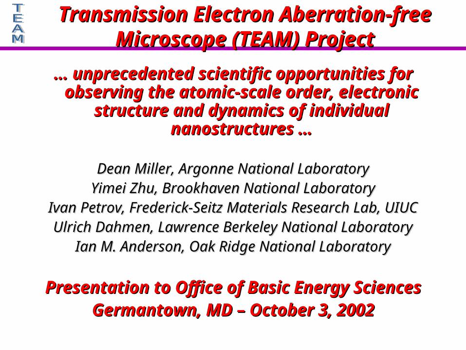
Feynman anticipates physical basis for chemical Feynman anticipates physical basis for chemical behavior and role of electron microscopebehavior and role of electron microscope
““It would be very easy to make an analysis of any complicated It would be very easy to make an analysis of any complicated chemical substance; all one would have to do would be to look at chemical substance; all one would have to do would be to look at it and see where the atoms are. The only trouble is that the it and see where the atoms are. The only trouble is that the electron microscope is one hundred times too poor … I put this electron microscope is one hundred times too poor … I put this out as a challenge: Is there no way to make the electron out as a challenge: Is there no way to make the electron microscope more powerful?”microscope more powerful?”
– – Richard P. Feynman, 1959, Richard P. Feynman, 1959, ““There’s Plenty of Room at the Bottom”There’s Plenty of Room at the Bottom”
Atomic-scale imaging plays a Atomic-scale imaging plays a uniqueunique role by defining quantum role by defining quantum mechanical boundary conditions for the electronic structure mechanical boundary conditions for the electronic structure calculations necessary to determine how nanostructures workcalculations necessary to determine how nanostructures work
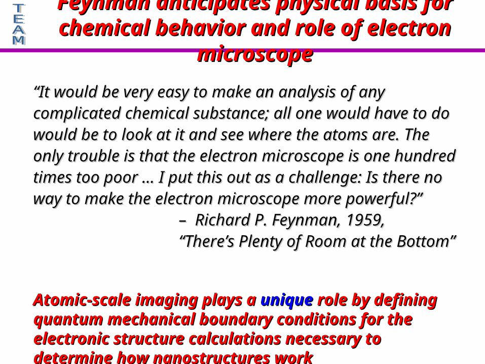
TEAM: extraordinary new scientific opportunities TEAM: extraordinary new scientific opportunities for direct observation of for direct observation of individualindividual nanostructures nanostructures
• three-dimensional atomic-scale structure, shape, and defect distribution
• spectroscopic identification and location of individual dopant atoms
• direct imaging of the atomic-scale structure of glasses
• electronic structure of individual point defects
• non-spherical charge density and valence electron distribution
• in-situ synthesis of novel nanoscale structures – e.g., electron-beam lithographic removal of individual columns of atoms
• in-situ observation of the synthesis of individual nanostructures
• in-situ observation of processing methods – e.g., thin film growth, oxidation, and deformation
• in-situ scientific investigation of dynamic materials responses to variations in external thermodynamic variables
– e.g., temperature, pressure, stress, chemical activity, and applied electric and magnetic fields
… … all with unprecedented spatial, spectral & temporal resolutionall with unprecedented spatial, spectral & temporal resolution
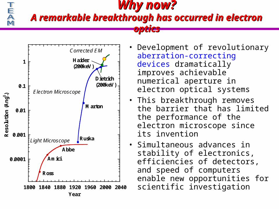
Why now?Why now?A remarkable breakthrough has occurred in electron opticsA remarkable breakthrough has occurred in electron optics
• Development of revolutionary aberration-correcting devices dramatically improves achievable numerical aperture in electron optical systems
• This breakthrough removes the barrier that has limited the performance of the electron microscope since its invention
• Simultaneous advances in stability of electronics, efficiencies of detectors, and speed of computers enable new opportunities for scientific investigation
0.0001
0.001
0.01
0.1
1
1800 1840 1880 1920 1960 2000 2040
Res
olu
tio
n (
An
g.-1)
Year
Electron Microscope
Light Microscope
Corrected EM
Ross
Amici
Abbe
Ruska
Marton
Dietrich(200keV)
Haider(200keV)

What does aberration correction buy us?What does aberration correction buy us?
0
200
400
600
800
1000
1200
-4 -2 0 2 4
0.8 Å1.2 Å2.0 Å
Inte
nsi
ty
distance (Å)
Greater sensitivity!Greater sensitivity!
Greater contrast!Greater contrast!
Smaller probes!Smaller probes!
Higher probe Higher probe intensity!intensity!
More signal!More signal!
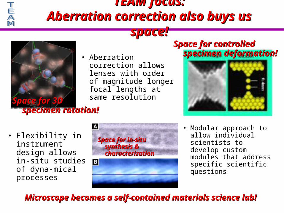
TEAM focus:TEAM focus:Aberration correction also buys us space!Aberration correction also buys us space!
Space for 3D Space for 3D specimen rotation!specimen rotation!
Space for controlled Space for controlled specimen deformation!specimen deformation!
Space for in-situ synthesis Space for in-situ synthesis & characterization& characterization
• Aberration correction allows lenses with order of magnitude longer focal lengths at same resolution
Microscope becomes a self-contained materials science lab!Microscope becomes a self-contained materials science lab!
• Modular approach to allow individual scientists to develop custom modules that address specific scientific questions
• Flexibility in instrument design allows in-situ studies of dyna-mical processes

Modular sample holder configurations enable Modular sample holder configurations enable in-situ measurements of materials behaviorin-situ measurements of materials behavior
Electron transparent window
Electron transparent window
Transportable specimen holder
Wide-bodiedstage
Front-end of stage
Volume available for experimental tools
MEMS specimen
Feed-through
DOE Basic Energy Sciences Microcharacterization User Centers, FS-MRL, ANL, BNL, LBL, ORNL
Modular MEMS specimen holder
for in situ studies(Initial designs can be employed in current
generation microscopes.)

The TEAM project: a science-based approach The TEAM project: a science-based approach for the development of aberration correctionfor the development of aberration correction
• Unique, state-of-the-art instruments designed to achieve the full potential of aberration-correcting optics– Hybrid instruments operating or on order today interface an
aberration correcting device to an earlier generation microscope
• Instruments tailored to in-situ scientific investigation of materials behavior at the nanoscale– Instruments designed in collaboration with non-microscopist
scientists to address specific classes of scientific problems
• Unique instrumentation and supporting expertise broadly available to general scientific community– Impact of investments maximized through location of
instruments within outward looking user centers

Status of TEAM ProjectStatus of TEAM Project
• First TEAM Workshop held following 2000 Stringer BESAC Panel Review endorsement of TEAM “vision document”
• Scientific Advisory Committee established– C.B. Carter, U Minnesota; J.A. Eades, Lehigh U; J. Silcox, Cornell U;
J.C.H..Spence, Arizona State U; R. Tromp, IBM
• Second TEAM Workshop, July 18-19, 2002 at LBNL, comprised 115 participants from 47 institutions– Strong participation from microscopy and general science communities,
with strong expressions of support for project
• Both TEM and STEM approaches to aberration correction under commercial development– Second generation TEM & STEM aberration correctors designed
• TEAM Advisory Committee recommends BES EBMCs develop full proposal to fund TEAM

Broad-based TEAM Workshop participation:Broad-based TEAM Workshop participation:18 universities, 13 companies, 7 national labs, 8 foreign & DOE18 universities, 13 companies, 7 national labs, 8 foreign & DOE
Stanford UniversityStanford University @ @ Massachusetts Institute of TechnologyMassachusetts Institute of Technology @ @ University of Illinois - Urbana ChampaignUniversity of Illinois - Urbana Champaign @ @ Lehigh UniversityLehigh University @ @ Arizona State UniversityArizona State University @ @ University of Illinois - ChicagoUniversity of Illinois - Chicago @ @ Case Western UniversityCase Western University @ @ North Carolina State UniversityNorth Carolina State University @ @ Vanderbilt UniversityVanderbilt University @ @ Northwestern UniversityNorthwestern University @ @ UC DavisUC Davis @ @ University of WashingtonUniversity of Washington @ @ UC Santa CruzUC Santa Cruz @ @ UC BerkeleyUC Berkeley @ @ Oregon State UniversityOregon State University @ @ University of MinnesotaUniversity of Minnesota @ @ AMDAMD @ @ University of PittsburghUniversity of Pittsburgh @ @ DupontDupont @ @ LumiledsLumileds @ @ GatanGatan @ @ PNNLPNNL @ @ HitachiHitachi @ @ IBMIBM @ @ JEOLJEOL @ @ LucentLucent @ @ MMFXMMFX @ @ FEIFEI @ @ LBNLLBNL @ @ LLNLLLNL @ @ ORNLORNL @ @ BNLBNL @ @ IntelIntel @ @ NionNion @ @ PGIPGI @ @ ANLANL @ @ SNLSNL @ @ Simon Fraser UniversitySimon Fraser University @ @ Chalmers UniversityChalmers University @ @ National Tsing Hua UniversityNational Tsing Hua University @ @ Regensburg UniversityRegensburg University @ @ Monash UniversityMonash University @ @ University of OrsayUniversity of Orsay @ @ CEOSCEOS @ @ DOEDOE @@

TEAM 2002 Workshop:TEAM 2002 Workshop:Scientific challenges identifiedScientific challenges identified
Aberration correction will create fundamentally new opportunities!Aberration correction will create fundamentally new opportunities!
• NanomaterialsNanomaterials – Dresselhaus, MIT– Synthesis, properties, assembly: electronic structure
• SemiconductorsSemiconductors – Eaglesham, Lucent– The end of the roadmap in Si technology: multiple nanoscale issues
• Magnetic materialsMagnetic materials – Siegmann, ETH– Fundamental understanding + utilization of magnetic
nanostructures
• Photonic materialsPhotonic materials – Craford, Lumileds– GaN will revolutionize the lighting industry: dopants, point defects
• Computational materials scienceComputational materials science – Diaz de la Rubia, LLNL– Convergence of theory and experiment: validate theory
• CatalysisCatalysis – Gai, Dupont– Energy, environment, transportation: controlled chemical processes
CO 2
Pt
Ti 4+
Ti 3+
O2-
e -CO O2

Opportunity for BESOpportunity for BESLocating TEAM at existing EBMCs maximizes scientific impactLocating TEAM at existing EBMCs maximizes scientific impact
• Well established user programs with missions that are aligned with BES science goals
• Proximity to nation’s BES-sponsored synchrotron light and neutron sources
• Closely coordinated with BES-funded Nanoscale Science Research Centers (NSRCs)
• Necessary infrastructure to support unique capability– broad scientific base, advanced scientific computing, technical support, etc.
• Strong record of instrumentation, technique development
• Extraordinary level of coordination among EBMCs in the development of electron beam microcharacterization user centers in general, and the TEAM initiative in particular
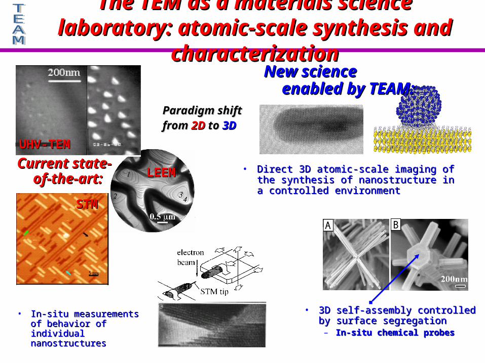
The TEM as a materials science laboratory: The TEM as a materials science laboratory: atomic-scale synthesis and characterizationatomic-scale synthesis and characterization
LEEMLEEM
STMSTM
Current state-Current state-of-the-art:of-the-art:
• Direct 3D atomic-scale imaging of the Direct 3D atomic-scale imaging of the synthesis of nanostructure in a controlled synthesis of nanostructure in a controlled environmentenvironment
UHV-TEMUHV-TEM
New science enabled New science enabled by TEAM:by TEAM:
• In-situ measurements of In-situ measurements of behavior of individual behavior of individual nanostructuresnanostructures
• 3D self-assembly controlled by 3D self-assembly controlled by surface segregationsurface segregation
– In-situ chemical probesIn-situ chemical probes
Paradigm shift Paradigm shift from from 2D2D to to 3D3D

New science through in-situ New science through in-situ multi-probe measurementsmulti-probe measurements
•STM/AFM•Four-point probes
•Indentation•Magnetic/ electric probes
e-
TEM
CNT
STM
STM
Doped nano-peapods; Yazdani, Science, 2002.
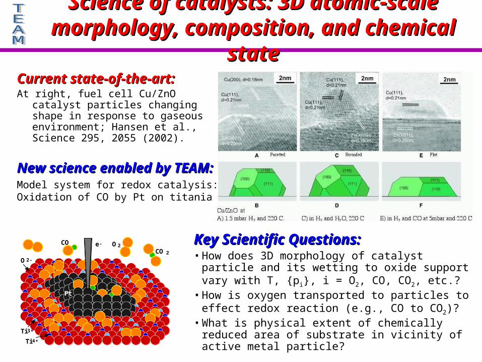
Science of catalysts: 3D atomic-scale Science of catalysts: 3D atomic-scale morphology, composition, and chemical statemorphology, composition, and chemical state
Key Scientific Questions:Key Scientific Questions:• How does 3D morphology of catalyst particle and its
wetting to oxide support vary with T, {pi}, i = O2, CO, CO2, etc.?
• How is oxygen transported to particles to effect redox reaction (e.g., CO to CO2)?
• What is physical extent of chemically reduced area of substrate in vicinity of active metal particle?
CO 2
Pt
Ti 4+
Ti 3+
O2-
e-CO O2
Current state-of-the-art:Current state-of-the-art:At right, fuel cell Cu/ZnO catalyst
particles changing shape in response to gaseous environment; Hansen et al., Science 295, 2055 (2002).
New science enabled by New science enabled by TEAM:TEAM:
Model system for redox catalysis:Oxidation of CO by Pt on titania

Science of semiconductors: 3D atomic-scale Science of semiconductors: 3D atomic-scale elemental distribution and nanoscale structureelemental distribution and nanoscale structure
Current state-of-the-art:Current state-of-the-art: New science enabled New science enabled by TEAM:by TEAM:
Local 3D elemental distribution through:
• Atomic resolution TEM & STEM tomography
• Single atom sensitivity in STEM across most of periodic table
Local nanoscale structure through:
• Nanocrystallography
Local elemental distribution key to developing GaN for solid state lighting; N, O distribution, amorphous material key for Si gate oxide
P.M. Voyles, D.A. Muller et al., Nature 416, 826 (2002)

Science of superconductors: simultaneous Science of superconductors: simultaneous imaging of structural defects, magnetic fieldsimaging of structural defects, magnetic fields
Lorentz micrograph of chain-latticestate of vortices in Bi-2212 filmSCIENCE 294, 5549, 2136 (2001)
Current state-of-the-art:Current state-of-the-art: New science enabled by TEAM:New science enabled by TEAM:● Location of vortices relative to
“pinning” structural defects via simultaneous high resolution and magnetic imaging
● Magnetic structure in vortex core● Proximity effects at interfaces
(e.g., magnetic superconducting)
MethodsMethods● Phase reconstruction (Coene, Thust):
defocus series enable long exp.times● Cs-corrected Lorentz TEM● Electron Holography● Lorentz STEM (0.1 nm dedicated)
● Resolution limit of 2 nm insufficient for simultaneous imaging of structural defects

Science of nanoscale functional materials: Science of nanoscale functional materials: non-spherical charge density, electron orbitals & spinnon-spherical charge density, electron orbitals & spin
Valence electron distribution in MgB2.Left: 2D line contour; Right: 3D map
BB
H=170 Oe H=300 Oe
Local magnetization & induction distribution of magnetic Co arrays
Current state-of-the-art:Current state-of-the-art:
35 Oe
New science enabled by TEAM:New science enabled by TEAM:• Non-spherical charge density &
electron orbitals via quantitative small-angle electron scattering
• Structure, bonding in aperiodic and amorphous materials
• Scientific understanding of spin dynamics & switching behavior of magnetic nano-arrays
MethodsMethods● Development of ultra-fast (104 frames/s)
solid-state detector● Position-sensitive, coherent interferometric
diffraction for 5D structure (3r + 2q)● Real-time phase retrieval for in-situ
mapping of electro- & magneto-static potential, field
0 Oe

Conclusion: TEAM will enable scientific Conclusion: TEAM will enable scientific discovery that can’t otherwise be achieveddiscovery that can’t otherwise be achieved
• Science-based approach for the development of aberration correcting electron optics
• Unique in providing 3D atomic-scale structure and dynamics of individual nanostructures– From 2D to 3D; from atomic columns to atoms ; from static to dynamic
• TEAM concept transforms electron microscope from imaging instrument into self-contained materials science laboratory– Individual scientists able to develop experimental modules that interface
with unique TEAM microscopes to address specific scientific questions
• New opportunities for materials discovery through combined atomic-scale characterization and in-situ synthesis– Direct observation of nanoscale synthesis at atomic resolution
• Feynman’s Holy Grail: unique role by defining the quantum mechanical boundary conditions for the electronic structure calculations necessary to determine how nanostructures work