Embed Size (px)
Citation preview
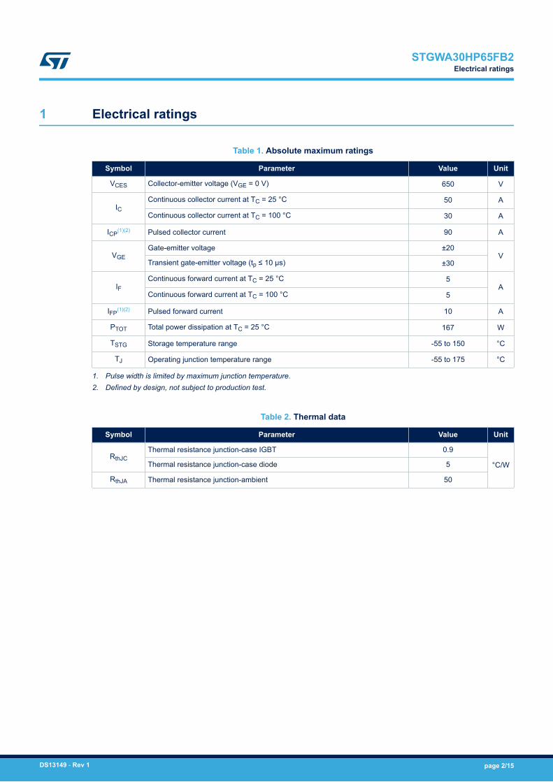
C(2, TAB)
E(3)NG1E3C2T
G(1)
Features• Maximum junction temperature : TJ = 175 °C• Low VCE(sat) = 1.65 V(typ.) @ IC = 30 A• Co-packaged protection diode• Minimized tail current• Tight parameter distribution• Low thermal resistance• Positive VCE(sat) temperature coefficient
Applications• Welding• Power factor correction
DescriptionThe newest IGBT 650 V HB2 series represents an evolution of the advancedproprietary trench gate field-stop structure. The performance of the HB2 series isoptimized in terms of conduction, thanks to a better VCE(sat) behavior at low currentvalues, as well as in terms of reduced switching energy. A diode used for protectionpurposes only is co-packaged in antiparallel with the IGBT. The result is a productspecifically designed to maximize efficiency for a wide range of fast applications.
Product status link
STGWA30HP65FB2
Product summary
Order code STGWA30HP65FB2
Marking G30HP65FB2
Package TO-247 long leads
Packing Tube
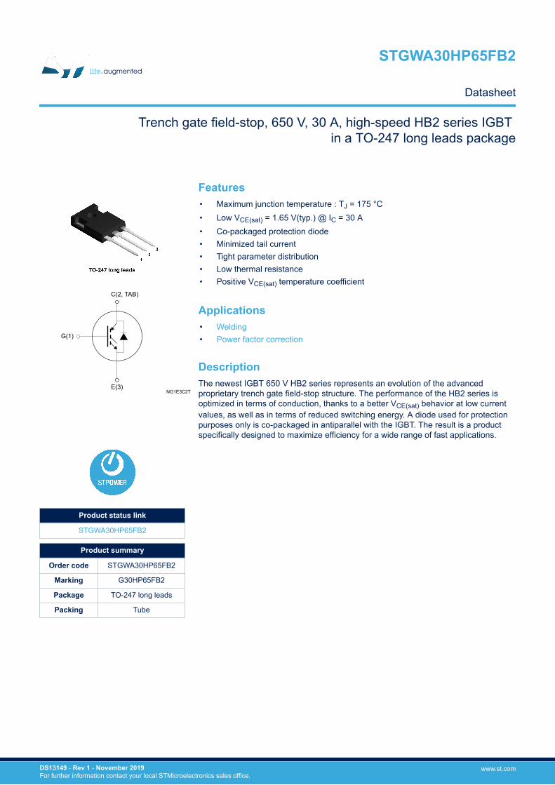
Trench gate field-stop, 650 V, 30 A, high-speed HB2 series IGBT in a TO-247 long leads package
STGWA30HP65FB2
Datasheet
DS13149 - Rev 1 - November 2019For further information contact your local STMicroelectronics sales office.
www.st.com
1 Electrical ratings
Table 1. Absolute maximum ratings
Symbol Parameter Value Unit
VCES Collector-emitter voltage (VGE = 0 V) 650 V
ICContinuous collector current at TC = 25 °C 50 A
Continuous collector current at TC = 100 °C 30 A
ICP(1)(2) Pulsed collector current 90 A
VGEGate-emitter voltage ±20
VTransient gate-emitter voltage (tp ≤ 10 μs) ±30
IFContinuous forward current at TC = 25 °C 5
AContinuous forward current at TC = 100 °C 5
IFP(1)(2) Pulsed forward current 10 A
PTOT Total power dissipation at TC = 25 °C 167 W
TSTG Storage temperature range -55 to 150 °C
TJ Operating junction temperature range -55 to 175 °C
1. Pulse width is limited by maximum junction temperature.2. Defined by design, not subject to production test.
Table 2. Thermal data
Symbol Parameter Value Unit
RthJCThermal resistance junction-case IGBT 0.9
°C/WThermal resistance junction-case diode 5
RthJA Thermal resistance junction-ambient 50
STGWA30HP65FB2Electrical ratings
DS13149 - Rev 1 page 2/15
2 Electrical characteristics
TC = 25 °C unless otherwise specified
Table 3. Static characteristics
Symbol Parameter Test conditions Min. Typ. Max. Unit
V(BR)CESCollector-emitter breakdownvoltage VGE = 0 V, IC = 1 mA 650 V
VCE(sat)Collector-emitter saturationvoltage
VGE = 15 V, IC = 30 A 1.65 2.1
VVGE = 15 V, IC = 30 A, TJ = 125 °C 1.85
VGE = 15 V, IC = 30 A, TJ = 175 °C 2.0
VF Forward on-voltage
IF = 5 A 2 2.8
VIF = 5 A, TJ = 125 °C 1.85
IF = 5 A, TJ = 175 °C 1.75
VGE(th) Gate threshold voltage VCE = VGE, IC = 1 mA 5 6 7 V
ICES Collector cut-off current VGE = 0 V, VCE = 650 V 25 µA
IGES Gate-emitter leakage current VCE = 0 V, VGE = ±20 V ±250 nA
Table 4. Dynamic characteristics
Symbol Parameter Test conditions Min. Typ. Max. Unit
Cies Input capacitance
VCE = 25 V, f = 1 MHz, VGE = 0 V
- 1570 -
pFCoes Output capacitance - 98 -
Cres Reverse transfer capacitance - 40 -
Qg Total gate chargeVCC = 520 V, IC = 30 A, VGE = 0 to 15 V
(see Figure 27. Gate charge test circuit)
- 90 -
nCQge Gate-emitter charge - 15.3 -
Qgc Gate-collector charge - 41.5 -
Table 5. Switching characteristics (inductive load)
Symbol Parameter Test conditions Min. Typ. Max. Unit
td(off) Turn-off delay time VCC = 400 V, IC = 30 A,
VGE = 15 V, RG = 6.8 Ω
(see Figure 26. Test circuit for inductiveload switching)
- 71 - ns
tf Current fall time - 41 - ns
Eoff (1) Turn-off switching energy - 310 - µJ
td(off) Turn-off delay time VCC = 400 V, IC = 30 A,
VGE = 15 V, RG = 6.8 Ω, TJ = 175 °C
(see Figure 26. Test circuit for inductiveload switching)
- 79 - ns
tf Current fall time - 105 - ns
Eoff (1) Turn-off switching energy - 643 - µJ
1. Including the tail of the collector current.
STGWA30HP65FB2Electrical characteristics
DS13149 - Rev 1 page 3/15
Table 6. Diode switching characteristics (inductive load)
Symbol Parameter Test conditions Min. Typ. Max. Unit
trr Reverse recovery time
IF = 5 A, VR = 400 V,
VGE = 15 V, di/dt = 1000 A/µs
(see Figure 29. Diode reverse recoverywaveform)
- 140 - ns
Qrr Reverse recovery charge - 21 - nC
Irrm Reverse recovery current - 6.6 - A
dIrr/dt Peak rate of fall of reverserecovery current during tb
- 430 - A/µs
Err Reverse recovery energy - 1.6 - µJ
trr Reverse recovery timeIF = 5 A, VR = 400 V,
VGE = 15 V, di/dt = 1000 A/µs,
TJ = 175 °C
(see Figure 29. Diode reverse recoverywaveform)
- 200 - ns
Qrr Reverse recovery charge - 47.3 - nC
Irrm Reverse recovery current - 9.6 - A
dIrr/dt Peak rate of fall of reverserecovery current during tb
- 428 - A/µs
Err Reverse recovery energy - 3.2 - µJ
STGWA30HP65FB2Electrical characteristics
DS13149 - Rev 1 page 4/15
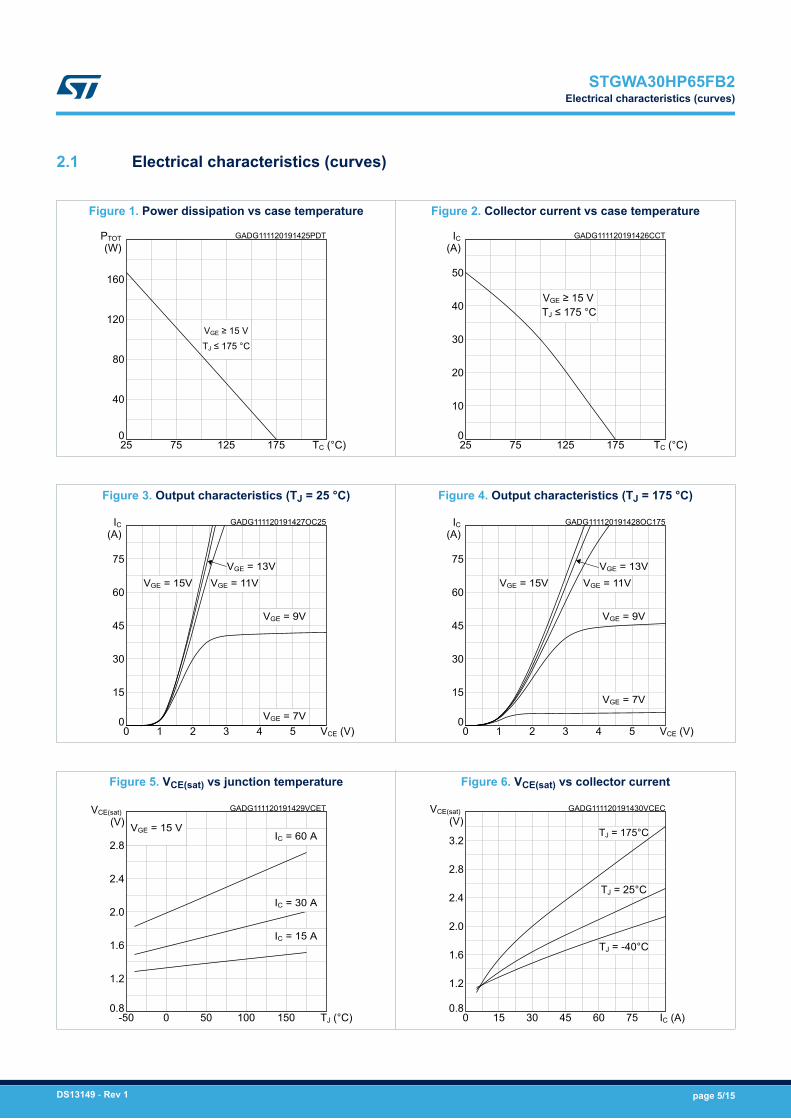
2.1 Electrical characteristics (curves)
Figure 1. Power dissipation vs case temperature
GADG111120191425PDT
160
120
80
40
025 75 125 175
PTOT (W)
TC (°C)
VGE ≥ 15 VTJ ≤ 175 °C
Figure 2. Collector current vs case temperature
GADG111120191426CCT
50
40
30
20
10
025 75 125 175
IC (A)
TC (°C)
VGE ≥ 15 VTJ ≤ 175 °C
Figure 3. Output characteristics (TJ = 25 °C)
GADG111120191427OC25
75
60
45
30
15
00 1 2 3 4 5
IC (A)
VCE (V)VGE = 7V
VGE = 9V
VGE = 11VVGE = 13V
VGE = 15V
Figure 4. Output characteristics (TJ = 175 °C)
GADG111120191428OC175
75
60
45
30
15
00 1 2 3 4 5
IC (A)
VCE (V)
VGE = 7V
VGE = 9V
VGE = 11VVGE = 13V
VGE = 15V
Figure 5. VCE(sat) vs junction temperature
GADG111120191429VCET
2.8
2.4
2.0
1.6
1.2
0.8-50 0 50 100 150 TJ (°C)
IC = 15 A
IC = 30 A
IC = 60 AVGE = 15 V
VCE(sat) (V)
Figure 6. VCE(sat) vs collector current
GADG111120191430VCEC
3.2
2.8
2.4
2.0
1.6
1.2
0.80 15 30 45 60 75 IC (A)
VCE(sat) (V)
TJ = -40°C
TJ = 25°C
TJ = 175°C
STGWA30HP65FB2Electrical characteristics (curves)
DS13149 - Rev 1 page 5/15
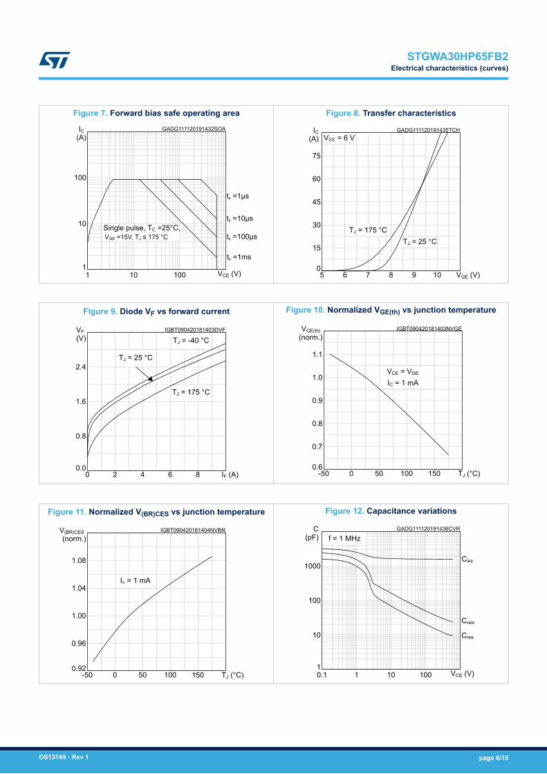
Figure 7. Forward bias safe operating area
GADG111120191432SOA
100
10
11 10 100
IC (A)
VCE (V)
Single pulse, TC =25°C,VGE =15V, TJ ≤ 175 °C
tp =10µs
tp =1ms
tp =100µs
tp =1µs
Figure 8. Transfer characteristics
75
60
45
30
15
05 6 7 8 9 10
IC (A)
VGE (V)
TJ = 25 °CTJ = 175 °C
VCE = 6 VGADG111120191435TCH
Figure 9. Diode VF vs forward current
IGBT090420181403DVF
2.4
1.6
0.8
0.00 2 4 6 8
VF (V)
IF (A)
TJ = 175 °C
TJ = 25 °C
TJ = -40 °C
Figure 10. Normalized VGE(th) vs junction temperature
IGBT090420181403NVGE
1.1
1.0
0.9
0.8
0.7
0.6-50 0 50 100 150
VGE(th) (norm.)
TJ (°C)
VCE = VGE
IC = 1 mA
Figure 11. Normalized V(BR)CES vs junction temperature
IGBT090420181404NVBR
1.08
1.04
1.00
0.96
0.92-50 0 50 100 150
V(BR)CES (norm.)
TJ (°C)
IC = 1 mA
Figure 12. Capacitance variations
GADG111120191436CVR
1000
100
10
10.1 1 10 100
C (pF)
VCE (V)
Cies
Coes
Cres
f = 1 MHz
STGWA30HP65FB2Electrical characteristics (curves)
DS13149 - Rev 1 page 6/15
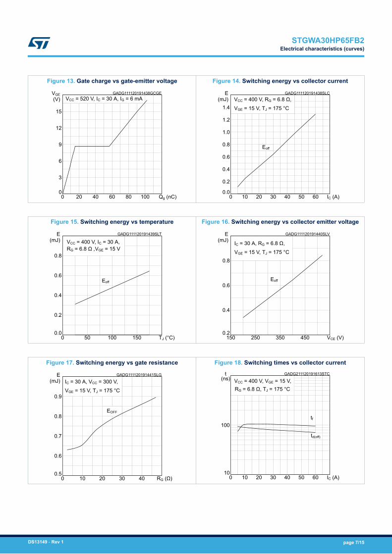
Figure 13. Gate charge vs gate-emitter voltage
GADG111120191438GCGE
15
12
9
6
3
00 20 40 60 80 100
VGE (V)
Qg (nC)
VCC = 520 V, IC = 30 A, IG = 6 mA
Figure 14. Switching energy vs collector current
GADG111120191438SLC
1.4
1.2
1.0
0.8
0.6
0.4
0.2
0.00 10 20 30 40 50 60
E (mJ)
IC (A)
VCC = 400 V, RG = 6.8 Ω,VGE = 15 V, TJ = 175 °C
Eoff
Figure 15. Switching energy vs temperature
GADG111120191439SLT
0.8
0.6
0.4
0.2
0.00 50 100 150
E (mJ)
TJ (°C)
Eoff
VCC = 400 V, IC = 30 A,RG = 6.8 Ω ,VGE = 15 V
Figure 16. Switching energy vs collector emitter voltage
GADG111120191440SLV
0.8
0.6
0.4
0.2150 250 350 450
E (mJ)
VCE (V)
Eoff
IC = 30 A, RG = 6.8 Ω,VGE = 15 V, TJ = 175 °C
Figure 17. Switching energy vs gate resistance
GADG111120191441SLG
0.9
0.8
0.7
0.6
0.50 10 20 30 40
E (mJ)
RG (Ω)
IC = 30 A, VCC = 300 V,VGE = 15 V, TJ = 175 °C
EOFF
Figure 18. Switching times vs collector currentGADG211120191613STC
100
100 10 20 30 40 50 60 IC (A)
tf
VCC = 400 V, VGE = 15 V,RG = 6.8 Ω, TJ = 175 °C
td(off)
(ns)t
STGWA30HP65FB2Electrical characteristics (curves)
DS13149 - Rev 1 page 7/15
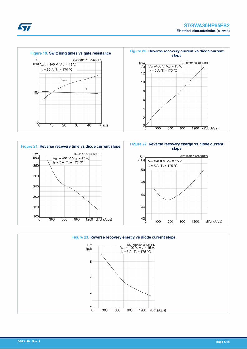
Figure 19. Switching times vs gate resistanceGADG111120191443SLG
100
100 10 20 30 40 Rg (Ω)
tf
td(off)
VCC = 400 V, VGE = 15 V,IC = 30 A, TJ = 175 °C
t(ns)
Figure 20. Reverse recovery current vs diode currentslope
IGBT120120160800RRC
12
10
8
6
4
2
00 300 600 900 1200
Irrm(A)
di/dt (A/µs)
VCC =400 V, VGE = 15 V,IF = 5 A, TJ =175 °C
Figure 21. Reverse recovery time vs diode current slope
IGBT120120160820RRT
350
300
250
200
150
1000 300 600 900 1200
trr (ns)
di/dt (A/μs)
VCC = 400 V, VGE = 15 V,IF = 5 A, TJ = 175 °C
Figure 22. Reverse recovery charge vs diode currentslope
IGBT120120160824RRQ
50
48
46
44
420 300 600 900 1200
Qrr(µC)
di/dt (A/µs)
VCC = 400 V, VGE = 15 V,IF = 5 A, TJ = 175 °C
Figure 23. Reverse recovery energy vs diode current slope
IGBT120120160826RRE
5
4
3
20 300 600 900 1200
Err(μJ)
di/dt (A/µs)
VCC = 400 V, VGE = 15 V,IF = 5 A, TJ = 175 °C
STGWA30HP65FB2Electrical characteristics (curves)
DS13149 - Rev 1 page 8/15
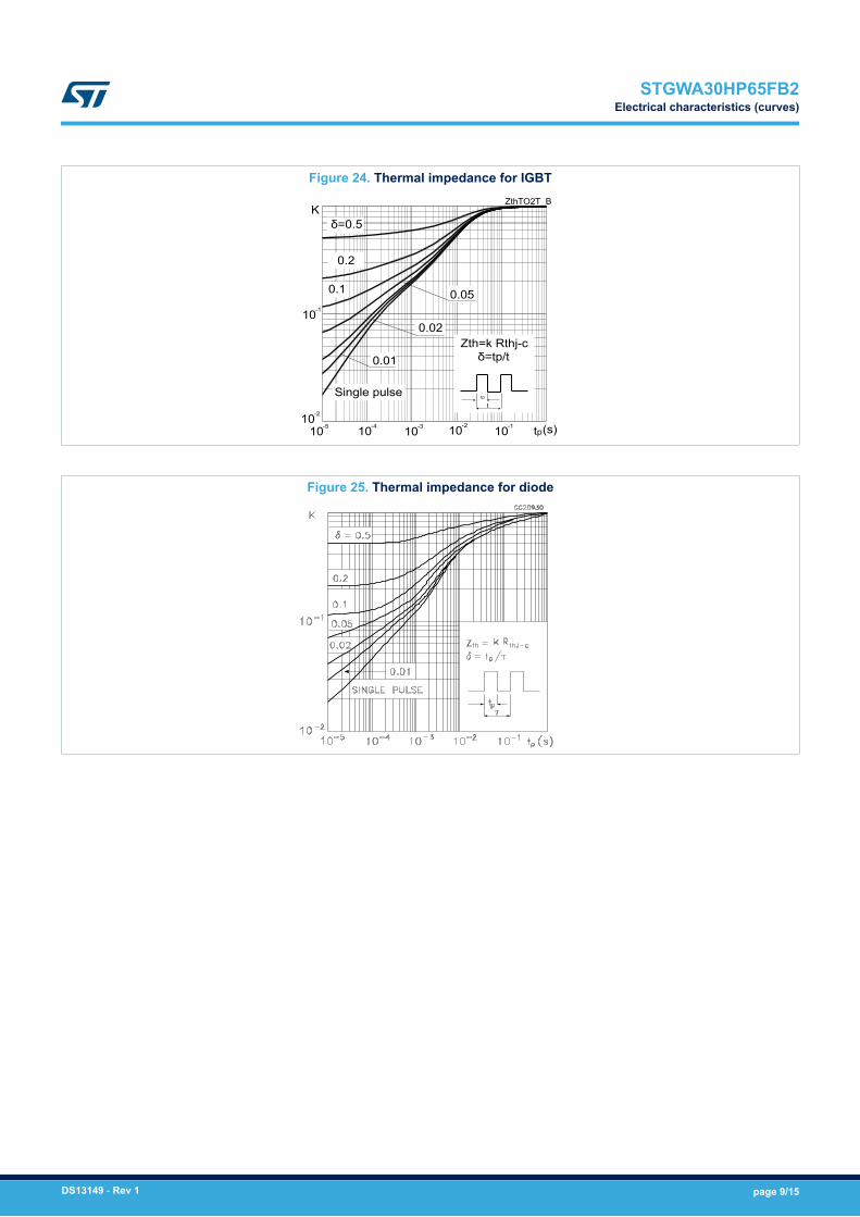
Figure 24. Thermal impedance for IGBT
10 10 10 10 10 tp(s)-5 -4 -3 -2 -110-2
10-1
K
0.2
0.05
0.02
0.01
0.1
Zth=k Rthj-cδ=tp/t
tp
t
Single pulse
δ=0.5
ZthTO2T_B
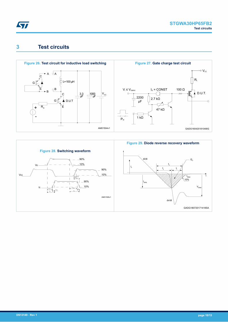
Figure 25. Thermal impedance for diode
STGWA30HP65FB2Electrical characteristics (curves)
DS13149 - Rev 1 page 9/15
3 Test circuits
Figure 26. Test circuit for inductive load switching
A AC
E
G
B
RG+
-
G
C 3.3µF
1000µF
L=100 µH
VCC
E
D.U.T
B
AM01504v1
Figure 27. Gate charge test circuit
GADG160420181048IG
RL
VCC
D.U.T.100 Ω IG = CONSTVi ≤ VGMAX
2200 μF
2.7 kΩ
PW1 kΩ
47 kΩ
Figure 28. Switching waveform
AM01506v1
90%
10%
90%
10%
VG
VCE
IC td(on)
ton
tr(Ion)
td(off)
toff
tf
tr(Voff)
tcross
90%
10%
Figure 29. Diode reverse recovery waveform
t
GADG180720171418SA
10%
VRRM
dv/dt
di/dt
IRRM
IF
trr
ts tf
Qrr
IRRM
STGWA30HP65FB2Test circuits
DS13149 - Rev 1 page 10/15
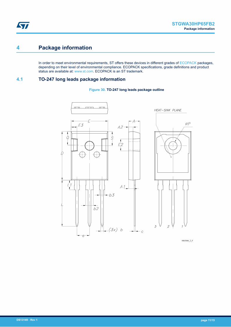
4 Package information
In order to meet environmental requirements, ST offers these devices in different grades of ECOPACK packages,depending on their level of environmental compliance. ECOPACK specifications, grade definitions and productstatus are available at: www.st.com. ECOPACK is an ST trademark.
4.1 TO-247 long leads package information
Figure 30. TO-247 long leads package outline
8463846_2_F
STGWA30HP65FB2Package information
DS13149 - Rev 1 page 11/15
Table 7. TO-247 long leads package mechanical data
Dim.mm
Min. Typ. Max.
A 4.90 5.00 5.10
A1 2.31 2.41 2.51
A2 1.90 2.00 2.10
b 1.16 1.26
b2 3.25
b3 2.25
c 0.59 0.66
D 20.90 21.00 21.10
E 15.70 15.80 15.90
E2 4.90 5.00 5.10
E3 2.40 2.50 2.60
e 5.34 5.44 5.54
L 19.80 19.92 20.10
L1 4.30
P 3.50 3.60 3.70
Q 5.60 6.00
S 6.05 6.15 6.25
STGWA30HP65FB2TO-247 long leads package information
DS13149 - Rev 1 page 12/15
Revision history
Table 8. Document revision history
Date Version Changes
05-Nov-2019 1 First release.
STGWA30HP65FB2
DS13149 - Rev 1 page 13/15
Contents
1 Electrical ratings . . . . . . . . . . . . . . . . . . . . . . . . . . . . . . . . . . . . . . . . . . . . . . . . . . . . . . . . . . . . . . . . . .2
2 Electrical characteristics. . . . . . . . . . . . . . . . . . . . . . . . . . . . . . . . . . . . . . . . . . . . . . . . . . . . . . . . . . .3
2.1 Electrical characteristics (curves) . . . . . . . . . . . . . . . . . . . . . . . . . . . . . . . . . . . . . . . . . . . . . . . . . 5
3 Test circuits . . . . . . . . . . . . . . . . . . . . . . . . . . . . . . . . . . . . . . . . . . . . . . . . . . . . . . . . . . . . . . . . . . . . . .10
4 Package information. . . . . . . . . . . . . . . . . . . . . . . . . . . . . . . . . . . . . . . . . . . . . . . . . . . . . . . . . . . . . .11
4.1 TO-247 long leads package information. . . . . . . . . . . . . . . . . . . . . . . . . . . . . . . . . . . . . . . . . . . 11
Revision history . . . . . . . . . . . . . . . . . . . . . . . . . . . . . . . . . . . . . . . . . . . . . . . . . . . . . . . . . . . . . . . . . . . . . . .13
STGWA30HP65FB2Contents
DS13149 - Rev 1 page 14/15
IMPORTANT NOTICE – PLEASE READ CAREFULLY
STMicroelectronics NV and its subsidiaries (“ST”) reserve the right to make changes, corrections, enhancements, modifications, and improvements to STproducts and/or to this document at any time without notice. Purchasers should obtain the latest relevant information on ST products before placing orders. STproducts are sold pursuant to ST’s terms and conditions of sale in place at the time of order acknowledgement.
Purchasers are solely responsible for the choice, selection, and use of ST products and ST assumes no liability for application assistance or the design ofPurchasers’ products.
No license, express or implied, to any intellectual property right is granted by ST herein.
Resale of ST products with provisions different from the information set forth herein shall void any warranty granted by ST for such product.
ST and the ST logo are trademarks of ST. For additional information about ST trademarks, please refer to www.st.com/trademarks. All other product or servicenames are the property of their respective owners.
Information in this document supersedes and replaces information previously supplied in any prior versions of this document.
© 2019 STMicroelectronics – All rights reserved
STGWA30HP65FB2
DS13149 - Rev 1 page 15/15


![CTB - 2016 January - HB2 update - ND.pptx [Read-Only] · HB2 system according to the HB2 legislative requirements and according to supporting policy documents that have been developed](https://img.pdfslide.net/doc/110x75/5b7a77537f8b9abf2d8c25cc/ctb-2016-january-hb2-update-ndpptx-read-only-hb2-system-according-to.jpg)