Embed Size (px)
Citation preview
®
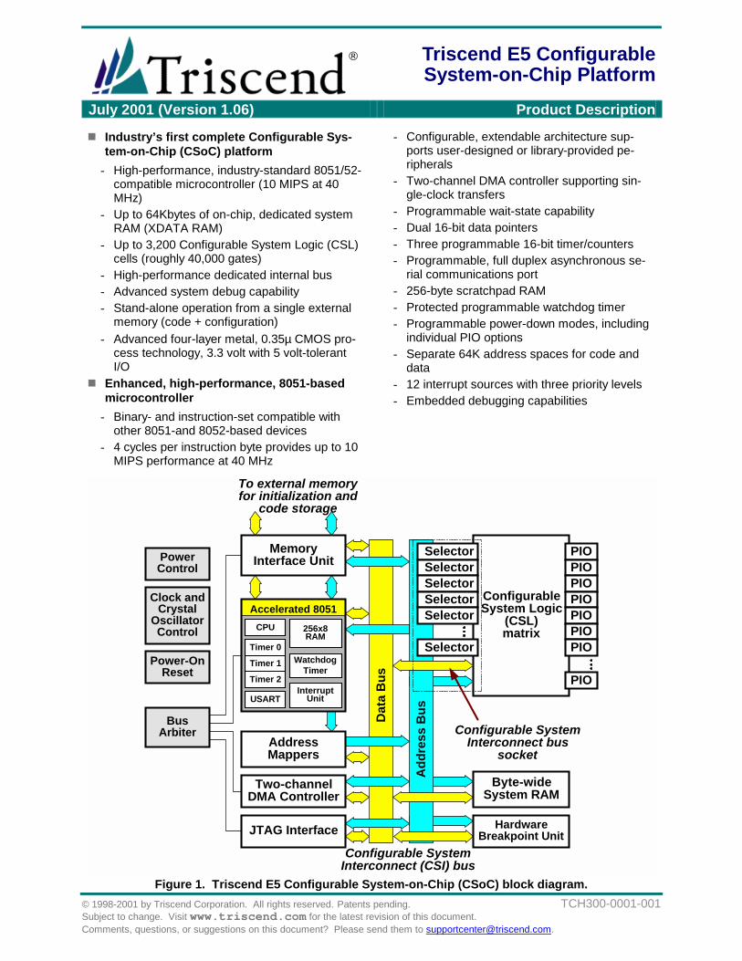
Triscend E5 Configurable System-on-Chip Platform
July 2001 (Version 1.06) Product Description
© 1998-2001 by Triscend Corporation. All rights reserved. Patents pending. TCH300-0001-001 Subject to change. Visit www.triscend.com for the latest revision of this document. Comments, questions, or suggestions on this document? Please send them to [email protected].
! Industry’s first complete Configurable Sys-tem-on-Chip (CSoC) platform
- High-performance, industry-standard 8051/52-compatible microcontroller (10 MIPS at 40 MHz)
- Up to 64Kbytes of on-chip, dedicated system RAM (XDATA RAM)
- Up to 3,200 Configurable System Logic (CSL) cells (roughly 40,000 gates)
- High-performance dedicated internal bus - Advanced system debug capability - Stand-alone operation from a single external
memory (code + configuration) - Advanced four-layer metal, 0.35µ CMOS pro-
cess technology, 3.3 volt with 5 volt-tolerant I/O
! Enhanced, high-performance, 8051-based microcontroller
- Binary- and instruction-set compatible with other 8051-and 8052-based devices
- 4 cycles per instruction byte provides up to 10 MIPS performance at 40 MHz
- Configurable, extendable architecture sup-ports user-designed or library-provided pe-ripherals
- Two-channel DMA controller supporting sin-gle-clock transfers
- Programmable wait-state capability - Dual 16-bit data pointers - Three programmable 16-bit timer/counters - Programmable, full duplex asynchronous se-
rial communications port - 256-byte scratchpad RAM - Protected programmable watchdog timer - Programmable power-down modes, including
individual PIO options - Separate 64K address spaces for code and
data - 12 interrupt sources with three priority levels - Embedded debugging capabilities
ConfigurableSystem Logic
(CSL)matrix
PIOPIOPIOPIOPIO
BusArbiter
PowerControl
Add
ress
Bus
SelectorSelector
Dat
a B
us
Clock andCrystal
OscillatorControl
Power-OnReset
To external memoryfor initialization and
code storage
Configurable SystemInterconnect (CSI) bus
Configurable SystemInterconnect bus
socket
CPU
USART
WatchdogTimer
InterruptUnit
256x8RAM
Timer 0
Timer 1
Timer 2
Accelerated 8051
Selector
SelectorSelector
AddressMappers
Two-channelDMA Controller
JTAG Interface
Byte-wideSystem RAM
HardwareBreakpoint Unit
MemoryInterface Unit
Selector
PIO
PIOPIO
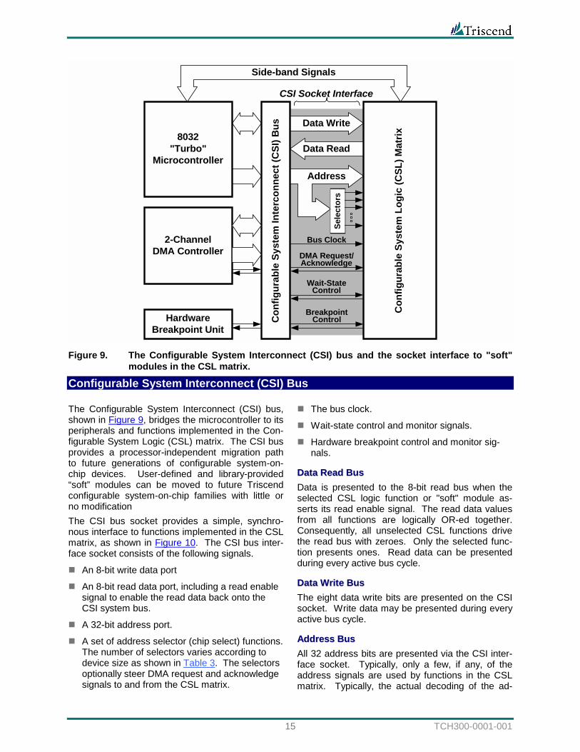
Figure 1. Triscend E5 Configurable System-on-Chip (CSoC) block diagram.
Triscend E5 Configurable System-on-Chip Platform
TCH300-0001-001 2
! Embedded Configurable System Logic (CSL) matrix
- Fast, flexible CSL logic cells support combina-torial logic, arithmetic, memory, sequential, and bus functions
- Up to 3,200 CSL cells per device - Easy, synchronous access to and from the
system bus - Programmable intercommunications network
between system bus, CSL cells, and pro-grammable I/O (PIO) pins
- Contention-free bi-directional bussing ! High-performance, dedicated Configurable
System Interconnect (CSI) system bus - 8-bit read and write data, 32-bit address - Up to 40 Mbytes/sec transfer rates - Simple, synchronous interface to CSL periph-
erals, seamless connection to the microcon-troller
- Multi-master bus with round-robin arbitration - Expandable to off-chip function through mem-
ory interface unit (MIU) - Flexible on-chip address decoders provide
easy access to CSL functions - Programmable wait-state support - Open standard - Forward compatible with future Triscend con-
figurable system-on-chip devices ! Enhanced programmable input/output (PIO)
ports - Up to 315 user-programmable I/O per device - Inputs, outputs, or bi-directional ports for the
microcontroller, dedicated peripherals, or pro-grammable logic peripherals
- Selectable output drive from 4 mA to 12 mA - BusMinder™ circuit provides pull-up, pull-
down, or weak-follower capability - Optional input hysteresis - Optional power-down operation, individually
selectable on every pin
- Input, output and output enable flip-flops for optimal set-up and clock-to-output perform-ance
- 5 volt tolerant inputs while operating at 3.3 volts
! Memory interface unit (MIU) for flexible, glue-less interface to external memory
- Direct connect interface to an external 256Kx8 memory for initialization and code storage
- Expandable from 18 up to 32 address lines - Variable-speed read/write timing simplifies in-
terface design - Access external peripherals by sharing MIU
data and address pins ! Two-channel advanced DMA controller
- Proxy bus masters for CSL “soft modules” - Up to 40 Mbytes/s transfer rate (1 byte/cycle) - Auto-initialization of channels - Multiple addressing modes - Software-initiated DMA requests - Optional interrupt at end of a transfer - Block data transfers - CRC checking - DMA channel request and acknowledge sig-
nals distributed to the CSL matrix ! Programmable power-down modes
- Selectively disable function during power-down
- Typically consumes less that 50 µA in full power-down mode
! On-chip oscillator, crystal oscillator ampli-fier, and clock distribution circuitry
! Four-pin IEEE 1149.1 JTAG interface port for download and debugging
- Supports SAMPLE/PRELOAD, EXTEST, IN-TEST, BYPASS, and IDCODE instructions
- 8051 reset and CSoC reset - Full access to the CSI system bus and all ad-
dressable locations
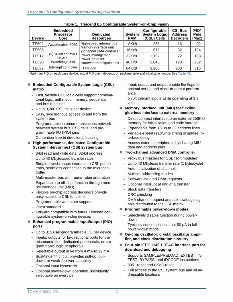
Table 1. Triscend E5 Configurable System-on-Chip Family
Device
Embedded Processor
Core Dedicated Resources
System RAM
Configurable System Logic
(CSL) Cells
CSI Bus Address
Decoders
PIO* Pins (Max)
TE502 8Kx8 256 16 92 TE505 16Kx8 512 32 124 TE512 32Kx8 1,152 72 188 TE520 40Kx8 2,048 128 252 TE532
Accelerated 8051
(3) 16-bit counters USART
Watchdog timer Interrupt controller
High-speed internal bus Memory interface unit 2-channel DMA controller Power management Power-on reset Hardware breakpoint unit JTAG port 64Kx8 3,200 200 316
* Maximum PIO on each base device, actual PIO count depends on package style and initialization mode. See Table 45.
3 TCH300-0001-001
! Multiple in-system programming modes - Unlimited, in-system programmability - Byte-wide using standard FLASH, EPROM, or
SRAM memories - Serially using serial sequential-access PROM
memories (SPROMs) - Via JTAG using internal system RAM to store
program code
- 'Stealth'-mode operation from internal RAM during battery-backed operation
! Dedicated in-system debugging, hardware breakpoint unit
- Two breakpoint units monitor system address, data, control, and processor instruction type
- Breakpoint indicator and control from Config-urable System Logic (CSL)
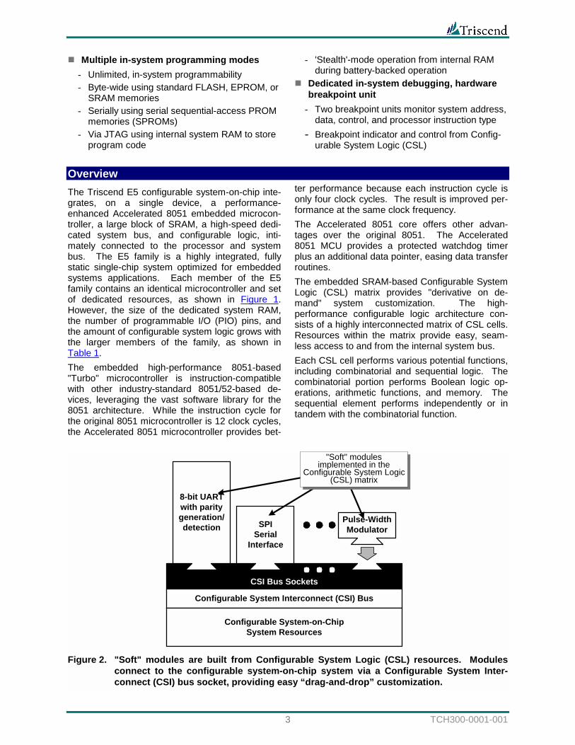
Overview The Triscend E5 configurable system-on-chip inte-grates, on a single device, a performance-enhanced Accelerated 8051 embedded microcon-troller, a large block of SRAM, a high-speed dedi-cated system bus, and configurable logic, inti-mately connected to the processor and system bus. The E5 family is a highly integrated, fully static single-chip system optimized for embedded systems applications. Each member of the E5 family contains an identical microcontroller and set of dedicated resources, as shown in Figure 1. However, the size of the dedicated system RAM, the number of programmable I/O (PIO) pins, and the amount of configurable system logic grows with the larger members of the family, as shown in Table 1. The embedded high-performance 8051-based "Turbo" microcontroller is instruction-compatible with other industry-standard 8051/52-based de-vices, leveraging the vast software library for the 8051 architecture. While the instruction cycle for the original 8051 microcontroller is 12 clock cycles, the Accelerated 8051 microcontroller provides bet-
ter performance because each instruction cycle is only four clock cycles. The result is improved per-formance at the same clock frequency. The Accelerated 8051 core offers other advan-tages over the original 8051. The Accelerated 8051 MCU provides a protected watchdog timer plus an additional data pointer, easing data transfer routines. The embedded SRAM-based Configurable System Logic (CSL) matrix provides "derivative on de-mand" system customization. The high-performance configurable logic architecture con-sists of a highly interconnected matrix of CSL cells. Resources within the matrix provide easy, seam-less access to and from the internal system bus. Each CSL cell performs various potential functions, including combinatorial and sequential logic. The combinatorial portion performs Boolean logic op-erations, arithmetic functions, and memory. The sequential element performs independently or in tandem with the combinatorial function.
Configurable System Interconnect (CSI) Bus
CSI Bus Sockets
Configurable System-on-ChipSystem Resources
SPISerial
Interface
Pulse-WidthModulator
8-bit UARTwith paritygeneration/detection
"Soft" modulesimplemented in the
Configurable System Logic(CSL) matrix
Figure 2. "Soft" modules are built from Configurable System Logic (CSL) resources. Modules
connect to the configurable system-on-chip system via a Configurable System Inter-connect (CSI) bus socket, providing easy “drag-and-drop” customization.
Triscend E5 Configurable System-on-Chip Platform
TCH300-0001-001 4
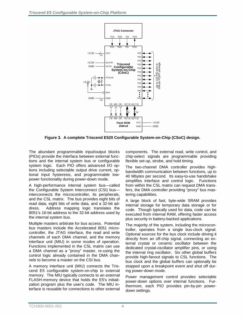
The abundant programmable input/output blocks (PIOs) provide the interface between external func-tions and the internal system bus or configurable system logic. Each PIO offers advanced I/O op-tions including selectable output drive current, op-tional input hysteresis, and programmable low-power functionality during power-down mode. A high-performance internal system bus—called the Configurable System Interconnect (CSI) bus— interconnects the microcontroller, its peripherals, and the CSL matrix. The bus provides eight bits of read data, eight bits of write data, and a 32-bit ad-dress. Address mapping logic translates the 8051's 16-bit address to the 32-bit address used by the internal system bus. Multiple masters arbitrate for bus access. Potential bus masters include the Accelerated 8051 micro-controller, the JTAG interface, the read and write channels of each DMA channel, and the memory interface unit (MIU) in some modes of operation. Functions implemented in the CSL matrix can use a DMA channel as a "proxy" master, re-using the control logic already contained in the DMA chan-nels to become a master on the CSI bus. A memory interface unit (MIU) connects the Tris-cend E5 configurable system-on-chip to external memory. The MIU typically connects to an external FLASH-memory device that holds the E5's initiali-zation program plus the user's code. The MIU in-terface is reusable for connections to other external
components. The external read, write control, and chip-select signals are programmable providing flexible set-up, strobe, and hold timing. The two-channel DMA controller provides high-bandwidth communication between functions, up to 40 Mbytes per second. Its easy-to-use handshake simplifies interface and control logic. Functions from within the CSL matrix can request DMA trans-fers, the DMA controller providing "proxy" bus mas-tering capabilities. A large block of fast, byte-wide SRAM provides internal storage for temporary data storage or for code. Though typically used for data, code can be executed from internal RAM, offering faster access plus security in battery-backed applications. The majority of the system, including the microcon-troller, operates from a single bus-clock signal. Optional sources for the bus clock include driving it directly from an off-chip signal, connecting an ex-ternal crystal or ceramic oscillator between the dedicated crystal-oscillator amplifier pins, or using the internal ring oscillator. Six other global buffers provide high-fanout signals to CSL functions. The bus clock and the global buffers can optionally be stopped upon a breakpoint event and shut off dur-ing power-down mode. Power management control provides selectable power-down options over internal functions. Fur-thermore, each PIO provides pin-by-pin power-down settings.
TriscendConfigurable
System-on-Chip(CSoC)
TCK TMS TDI TDO
CE- OE- D[7:0] A[17:0]WE-
188
PIO
RST-
XTALIN
XTALPIO
PIO
PIO
PIO
PIOVSYS
+3.3VPIO
PIO
PIO
PIO
PIO
PIO
Up
to 1
25 P
IO p
ins
in20
8-pi
n PQ
FP p
acka
ge
+3.3V16
VCC
GND28
GND
JTAG Connector
TCK TMS TDI TDO
Flash ROM256Kx8
CE- WE- OE- D[7:0] A[17:0]
SLAVE-
+3.3V
VCC
GND GND+3.3V
GND
Figure 3. A complete Triscend E520 Configurable System-on-Chip (CSoC) design.
5 TCH300-0001-001
The E5 configurable system-on-chip, like other ad-vanced processors, is built from leading-edge static CMOS technology. The E5 device is infinitely in-system programmable. A power-on reset circuit guarantees proper start-up operation after power is asserted. There are various initialization (boot-strapping) modes to support different application requirements. The E5 can load itself automatically after power-on from an external, byte-wide boot memory. Optionally, the E5's configuration data is stored in a serial sequential-access PROM. In se-rial mode, the user's code is copied to and exe-cuted from the internal SRAM. Serial mode frees a number of device pins so that they can be used as user-defined PIO pins. In security-conscious applications, the user's pro-gram is stored in internal RAM and battery-backed using external circuitry. If the E5 configurable sys-tem-on-chip is in ‘stealth’ mode, it boots from inter-nal RAM when VCC is re-applied after battery back up. Stealth mode optionally disables the JTAG interface port and disables external fetches via the MIU. An internal initialization boot ROM controls the start of initialization during power-on after the RST- pin is released. The primary purpose of the initializa-tion boot ROM is to find the user's initialization data and code stored in the secondary boot code, usu-ally held in PROM. Initialization programs can also be downloaded directly to internal SRAM through the JTAG port. Likewise, initialization programs can be written to external flash via JTAG through the MIU interface. Besides downloading initialization programs, the JTAG port offers nearly full access to the microcontroller, peripherals, and CSL functions to aid in debugging. The JTAG interface can become a bus master on the internal CSI bus. During system debugging, the JTAG port also sets up the internal hardware breakpoint unit. The hardware breakpoint unit contains two func-tions that monitor the 8-bit read or write data bus, the 32-bit internal address bus, control signals and the type of processor instruction (code or data ac-cess). Upon a predefined set of conditions, the breakpoint unit halts execution of the application program. Via JTAG control, the user can single-step instruction execution of the processor. Together, the Accelerated 8051 microcontroller, its dedicated peripherals, the on-chip RAM, the inter-nal CSI system bus, and the CSL matrix and PIOs form a powerful, integrated configurable system.
Accelerated 8051 Microcontroller The Triscend E5 8051-based configurable system-on-chip is fully instruction set compatible with other industry-standard 8051/8052 microcontrollers. It includes the resources of the standard 8051 includ-ing three 16-bit timer/counters; a full-duplex serial port and twelve interrupt sources with three priority levels. The E5 features a performance-enhanced 8-bit CPU with a redesigned core processor, reducing unnecessary clock and memory cycles. The in-struction cycle of a standard 8051 is twelve clock cycles while the Triscend E5 reduces this to four clock cycles for the majority of instructions, thereby improving performance by an average of 1.5 to 3 times. This naturally speeds up the execution of the in-structions. Consequently, the E5 offers more processing power compared to the original 8051, even using the same frequency crystal. For a given throughput, the E5 can be operated from a lower-frequency clock than the original 8051, re-ducing power consumption. The E5 also provides dual Data Pointers (DPTRs) to boost block data memory transfers.
PPrrooggrraammmmaabbllee II//OO PPoorrttss The original 8051 offers up to four 8-bit ports, a total up to 32 lines. In the E5, the 8051 processor core is embedded with other functions. The proc-essor optionally connects to as many PIO pins as required by the application.
UUAARRTT The Triscend E5's UART is a superset of the UART in the original 8051 family, though offers timing compatibility. The UART provides enhanced features such as automatic address recognition and frame error detection.
TTiimmeerrss The E5's 8051-based microcontroller has three 16-bit timers that are functionally similar to the timers of the original 8051 family. When used as timers, they optionally operate at either 4 clocks or 12 clocks per count, thus providing a mode that emu-lates the timing of the original 8051. The E5 also features a protected watchdog timer. This timer is used as a system monitor or to time a very long period.
Triscend E5 Configurable System-on-Chip Platform
TCH300-0001-001 6
IInntteerrrruuppttss The Interrupt structure in the Triscend configurable system-on-chip is slightly different from that of the original 8051. Due to the presence of additional features and peripherals, the number of interrupt sources and vectors is increased.
DDaattaa PPooiinntteerrss The original 8051 had only one 16-bit Data Pointer (DPL, DPH). In the E5, there is an additional 16-bit Data Pointer (DPL1, DPH1). This new Data Pointer inhabits two previously unused SFR loca-tions in the original 8051.
PPoowweerr MMaannaaggeemmeenntt Like the original 80C31, the E5 provides Idle and Power-Down modes of operation. Idle mode stops the MCU while the timers, serial port and interrupt block continues to operate. Power-Down mode optionally stops all the clocks and completely halts chip operation, the lowest power-consumption state.
PPoowweerr--OOnn rreesseett The Triscend configurable system-on-chip has an on-chip Power-On Reset facility. This eliminates the external capacitor-resistor network required in original 8051 designs.
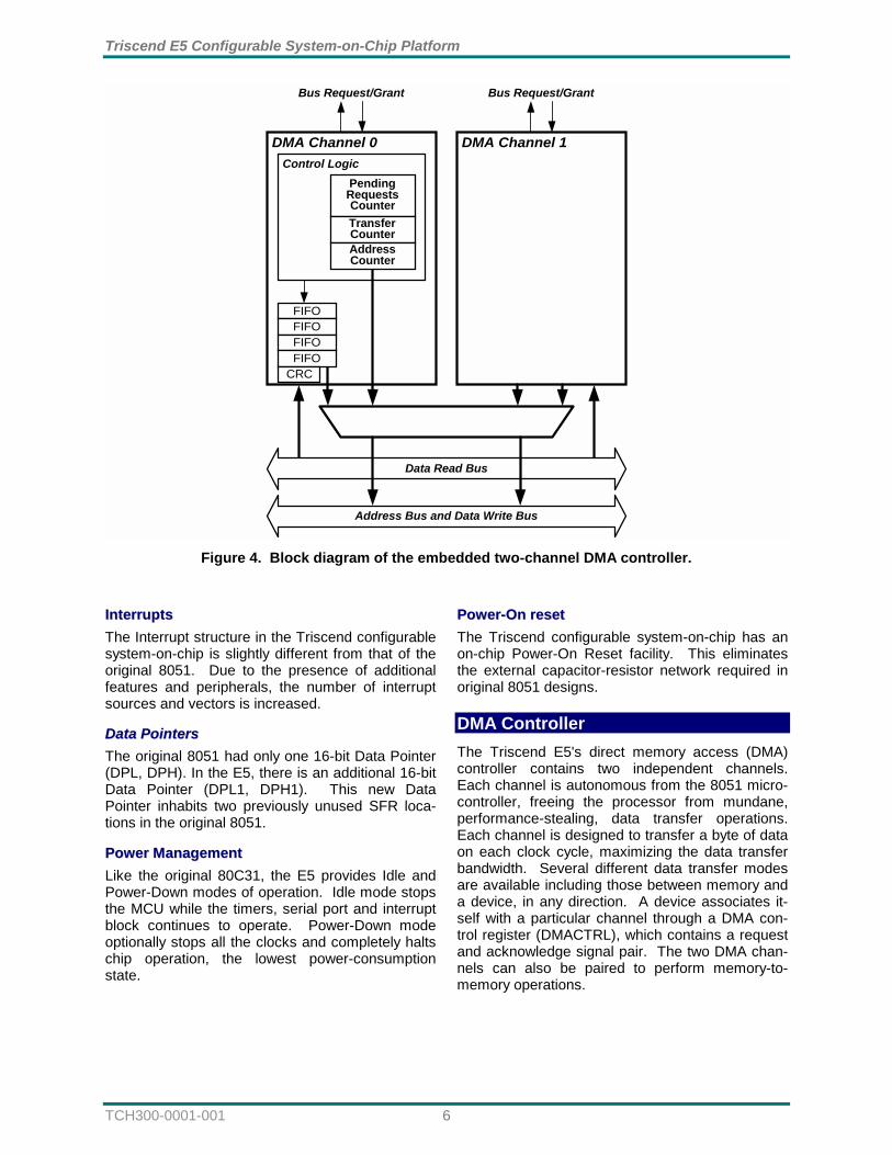
DMA Controller The Triscend E5's direct memory access (DMA) controller contains two independent channels. Each channel is autonomous from the 8051 micro-controller, freeing the processor from mundane, performance-stealing, data transfer operations. Each channel is designed to transfer a byte of data on each clock cycle, maximizing the data transfer bandwidth. Several different data transfer modes are available including those between memory and a device, in any direction. A device associates it-self with a particular channel through a DMA con-trol register (DMACTRL), which contains a request and acknowledge signal pair. The two DMA chan-nels can also be paired to perform memory-to-memory operations.
Control LogicDMA Channel 0 DMA Channel 1
FIFOFIFOFIFOFIFO
CRC
Address Bus and Data Write Bus
Data Read Bus
PendingRequestsCounterTransferCounterAddressCounter
Bus Request/Grant Bus Request/Grant
Figure 4. Block diagram of the embedded two-channel DMA controller.
7 TCH300-0001-001
The main features of the DMA controller unit are: ! Two independent channels for device or mem-
ory transfers
! Transfer rates up to 40 Mbytes/sec
! Auto-initialization of channels
! Programmable transfer parameters
! Multiple addressing modes
! Interrupt capabilities
! Memory-to-memory transfers capabilities
! Block transfers
! Software-initiated DMA requests
! Four-byte FIFO
! Asynchronous request/acknowledge handshake
! CRC on DMA data stream
FFuunnccttiioonnaall DDeessccrriippttiioonn The DMA unit is composed of two channels as shown in Figure 4. A set of parameters defines the operation for a specific DMA channel, including the memory starting address and starting transfer count, the direction of the transfer, and a variety of other transfer characteristics. Each channel has its own register set. The control logic block contains the address counter, the current transfer count, the pending requests counter and channel control logic. The data FIFO serves as a temporary buffer between the I/O device and memory. The CSI bus arbiter treats each channel as independent bus masters.
DDMMAA IInniittiiaalliizzaattiioonn aanndd TTeerrmmiinnaattiioonn The DMA channels are initialized through their pro-grammable registers. Once the transfer parame-ters have been programmed, the DMA channel must first be enabled and the transfer initialized. Setting the EN bit in the respective DMA_CTRLx_0 register enables the DMA channel. Once enabled, the DMA channel accepts requests. At that point, the DMA accept requests but cannot service them. A transfer is initialized by setting the INIT bit. Upon initialization, the first DMA request loads the start address and start count into their respective count-ers. The INIT bit is reset by hardware and the DMA controller services the request. Software can detect that a transfer has been initiated when the INIT bit is cleared. The next transfer parameters can be updated and the INIT bit set. Requests are processed on a cycle basis. Re-quests lasting more than one clock cycle are inter-preted as multiple requests. If the DMA cannot
process all the incoming requests, a Pending Re-quest Counter keeps track of such requests. A total of 64K pending requests are possible. If the EN is cleared in the middle of a block transfer, any subsequent requests are ignored by the DMA and by the pending request counter. The counters can be read through software until it is reset. The counters are initialized either by the CLR bit or by enabling the DMA channel. In case a DMA channel is not responding properly, it is possible to reset it through the CLR bit in the control register. Once the CLR bit is set, the DMA channel is in a reset state. It exits this state only after the CLR bit is cleared. After a power-on reset or other system-wide reset, CLR is set. A block transfer normally completes when the transfer counter reaches zero. At that point, de-pending on the mode, the DMA transfer either stops or continues. The DMA continues with the next block transfer if the INIT bit is set, or if con-tinuous mode is enabled. Resetting the DMA chan-nel also terminates a block transfer. The latter method should be used very carefully.
AAbboorrttiinngg aa DDMMAA ttrraannssffeerr Software can cleanly abort an operation in the mid-dle of a DMA transfer. Once the user detects that the current DMA transfer can be aborted, the DMA channel can be disabled cleanly by clearing the EN bit. The next step is to reset the DMA channel logic, accomplished by setting the CLR bit. Only one clock cycle is necessary to reset the DMA channel logic. Once the CLR is cleared, the DMA channel is again ready to use. Except for a few important control bits (refer to the reset values of each field of the DMA registers), the rest of the configuration registers will have kept their previ-ously programmed values. By writing a few com-mand bits to the control register, the previous transfer could be repeated.
TTrraannssffeerr hhaannddsshhaakkiinngg The DMA controller always does the read transfer first and stores the data into its temporary FIFO. Then it performs the write transfer.
TTrraannssffeerr MMooddeess This section describes the basic DMA transfer types and features. Some of these transfer modes can be combined to form more complex and pow-erful operations.
SSiinnggllee TTrraannssffeerr MMooddee In this mode, the DMA initiates a single byte trans-fer for each request. If the requests are asserted during every cycle, then the DMA controller at-tempts to service the requests as fast as it can. The DMA services requests until the transfer count
Triscend E5 Configurable System-on-Chip Platform
TCH300-0001-001 8
reaches zero. At that point, the transfer is com-pleted. This is the default mode.
BBlloocckk TTrraannssffeerr MMooddee In this mode, a single request initiates a transfer of an entire block of data. Upon receiving the re-quest, the DMA controller starts transferring data until the transfer count reaches zero. If a request is received at any time during the block transfer, the request is recorded in the Pending Requests Counter. The new request is serviced at the end of the current block transfer.
SSooffttwwaarree RReeqquueesstt When this mode is active, the DMA controller re-sponds to a DMA request initiated from software. Setting the SFTREQ bit in the DMA channel control register enables this mode. Software can then re-quest a DMA transfer. Software requests that can-not currently be served are recorded in the pending request counter. A software request is cleared by hardware on the cycle following the set operation. If the software request is set while the DMA chan-nel is disabled, then the request is ignored.
SSiinnggllee IInniittiiaalliizzaattiioonn Setting the INIT bit initializes a transfer. Upon re-ceiving the first request, the INIT bit is reset by hardware and the single, software or block transfer continues until the transfer count reaches zero. At that point, the DMA controller waits for a new ini-tialization command.
CCoonnttiinnuuoouuss AAuuttoo--IInniittiiaalliizzaattiioonn Setting the CONT initiates a transfer similar to the INIT bit, but upon completion of the current trans-fer, the DMA controller automatically reinitializes as if the INIT bit were set again. Automatic refresh of some external display is one potential application of this mode.
MMeemmoorryy--ttoo--MMeemmoorryy TTrraannssffeerr By pairing the channels together, the DMA control-ler supports memory-to-memory transfers. The channel that reads the data from memory, is the master, and the other channel, which writes the data back into memory, is the slave. Setting the PAIR bit in the control register of both channels enables this mode. Transfers are initiated using the master's control register. However, the slave channel must be enabled and its transfer parame-ters set correctly.
LLiinnkkeedd ttrraannssffeerrss Linked transfers are possible using a single-initialization, software block transfer. The parame-ters of the first block transfers are programmed into the appropriate control registers and the transfer is
initiated through the INIT bit and the SFTREQ bit. Once the INIT bit is cleared by hardware—meaning the DMA channel has initiated the transfer—software loads the address and transfer count pa-rameters of the next block of data. After loading the parameters, software sets the INIT and SFTREQ bits. Upon completion of the first block transfer, the DMA channel loads the new parame-ters and initiates the new transfer. Software re-peats the previous steps until it reaches the end of the linked list.
BBuuss AAddddrreessss GGeenneerraattiioonn Each DMA channel generates a memory address for every request. The first address of a block transfer is the starting address, held in starting ad-dress control register. This address value is then loaded into the current address counter upon the first request of a block transfer. Once the address is broadcast to memory, it is updated for the next request. The addressing option is configured through two of the DMA channel's control register bits, as shown in Table 2. For debug purposes, the current address of a block transfer as well as the current count are visible to software.
DDaattaa FFIIFFOO The data FIFO serves as a temporary buffer be-tween the requesting I/O device and memory. Be-cause of the CSI bus structure and the multi-master handshaking, four locations are required.
CCRRCC FFeeaattuurree A cyclic redundancy check (CRC) can be per-formed on a single DMA stream. The CRC logic monitors the Data Read bus as it enters the DMA's FIFOs. The CRC logic is shared between the two DMA channels and is enabled for either one of the channels by setting the CRC_EN bit in the corre-sponding DMA channel control register. A 0-to-1 transition on CRC_EN resets the CRC shift-register to zero. Once enabled, the CRC logic is activated any time a byte of data is written into a FIFO. Once a transfer is completed, the output of the CRC reg-ister can be read by software, and the CRC signa-ture can be compared with the expected value. The CRC logic uses a CRC-CCITT 16-bit divisor polynomial, as shown in the equation below. The algorithm is capable of detecting any one, two or an even number of bits in error as well as a large number of burst errors.
X16 + X12 + X5 + 1
IInntteerrrruuppttss GGeenneerraattiioonn The DMA controller can generate interrupts upon the following three events.
9 TCH300-0001-001
Transfer terminal count: This event is generated when a block transfer is complete (when the trans-fer counter reaches its terminal count of 0). Transfer Initialization: This event is generated upon the first request of block transfer if the INIT bit is set. Pending Request Overflow: This event is gener-ated when the pending request counter overflows, indicating that the DMA controller cannot keep up with the number of incoming requests. The status of these events is recorded in the inter-rupt status register, independent of their corre-sponding interrupt-enable bits. The status bits are reset by software by writing a one into them. Writ-ing a zero does not affect the state of any status bits. Some of the status bits are also cleared by some hardware action (refer to "DMA Interrupt Register").
CCoonnffiigguurraattiioonn RReeggiisstteerrss Each channel has a set of 21 bytes of control and status registers. Some registers are used to pro-gram a specific DMA channel or to query its status.
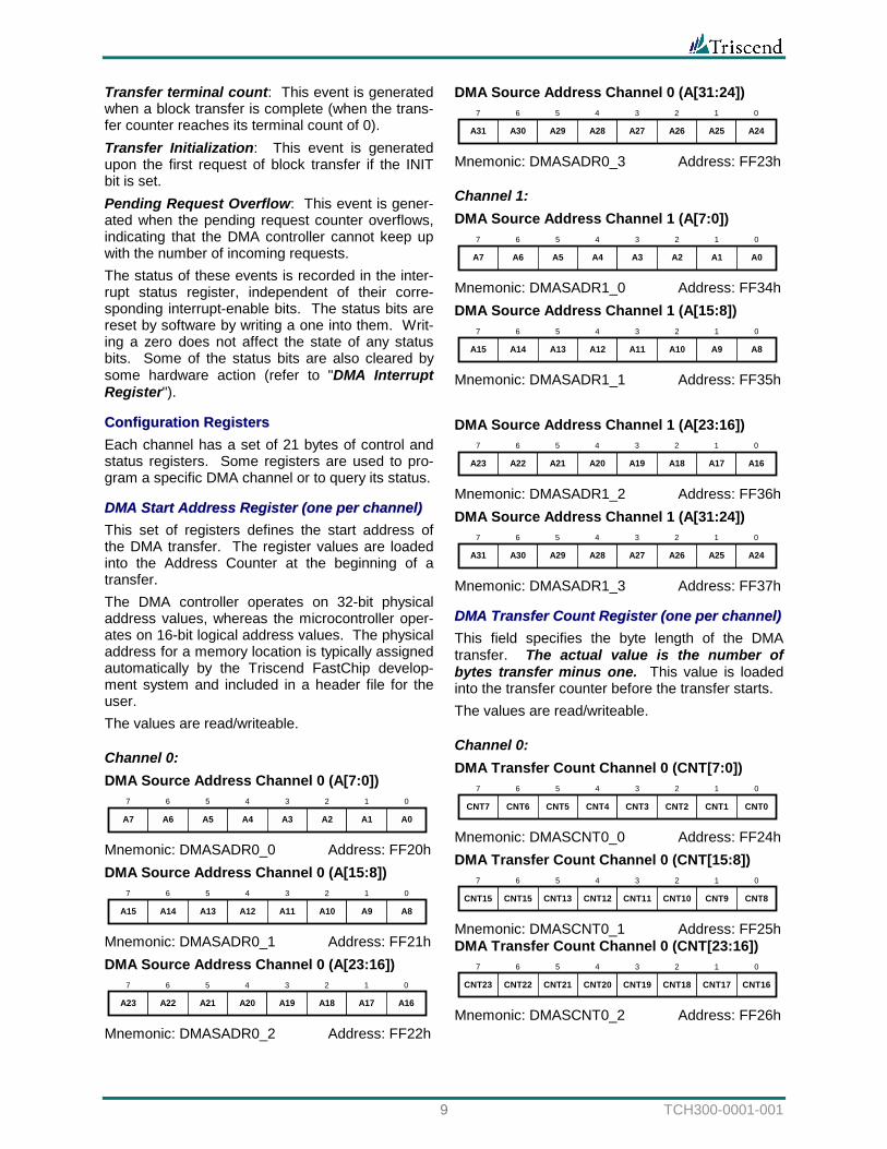
DDMMAA SSttaarrtt AAddddrreessss RReeggiisstteerr ((oonnee ppeerr cchhaannnneell)) This set of registers defines the start address of the DMA transfer. The register values are loaded into the Address Counter at the beginning of a transfer. The DMA controller operates on 32-bit physical address values, whereas the microcontroller oper-ates on 16-bit logical address values. The physical address for a memory location is typically assigned automatically by the Triscend FastChip develop-ment system and included in a header file for the user. The values are read/writeable.
Channel 0: DMA Source Address Channel 0 (A[7:0])
A7 A6 A5 A4 A3 A2 A1 A0
7 6 5 4 3 2 1 0
Mnemonic: DMASADR0_0 Address: FF20h DMA Source Address Channel 0 (A[15:8])
A15 A14 A13 A12 A11 A10 A9 A8
7 6 5 4 3 2 1 0
Mnemonic: DMASADR0_1 Address: FF21h DMA Source Address Channel 0 (A[23:16])
A23 A22 A21 A20 A19 A18 A17 A16
7 6 5 4 3 2 1 0
Mnemonic: DMASADR0_2 Address: FF22h
DMA Source Address Channel 0 (A[31:24])
A31 A30 A29 A28 A27 A26 A25 A24
7 6 5 4 3 2 1 0
Mnemonic: DMASADR0_3 Address: FF23h
Channel 1: DMA Source Address Channel 1 (A[7:0])
A7 A6 A5 A4 A3 A2 A1 A0
7 6 5 4 3 2 1 0
Mnemonic: DMASADR1_0 Address: FF34h DMA Source Address Channel 1 (A[15:8])
A15 A14 A13 A12 A11 A10 A9 A8
7 6 5 4 3 2 1 0
Mnemonic: DMASADR1_1 Address: FF35h DMA Source Address Channel 1 (A[23:16])
A23 A22 A21 A20 A19 A18 A17 A16
7 6 5 4 3 2 1 0
Mnemonic: DMASADR1_2 Address: FF36h DMA Source Address Channel 1 (A[31:24])
A31 A30 A29 A28 A27 A26 A25 A24
7 6 5 4 3 2 1 0
Mnemonic: DMASADR1_3 Address: FF37h
DDMMAA TTrraannssffeerr CCoouunntt RReeggiisstteerr ((oonnee ppeerr cchhaannnneell)) This field specifies the byte length of the DMA transfer. The actual value is the number of bytes transfer minus one. This value is loaded into the transfer counter before the transfer starts. The values are read/writeable.
Channel 0: DMA Transfer Count Channel 0 (CNT[7:0])
CNT7 CNT6 CNT5 CNT4 CNT3 CNT2 CNT1 CNT0
7 6 5 4 3 2 1 0
Mnemonic: DMASCNT0_0 Address: FF24h DMA Transfer Count Channel 0 (CNT[15:8])
CNT15 CNT15 CNT13 CNT12 CNT11 CNT10 CNT9 CNT8
7 6 5 4 3 2 1 0
Mnemonic: DMASCNT0_1 Address: FF25h DMA Transfer Count Channel 0 (CNT[23:16])
CNT23 CNT22 CNT21 CNT20 CNT19 CNT18 CNT17 CNT16
7 6 5 4 3 2 1 0
Mnemonic: DMASCNT0_2 Address: FF26h
Triscend E5 Configurable System-on-Chip Platform
TCH300-0001-001 10
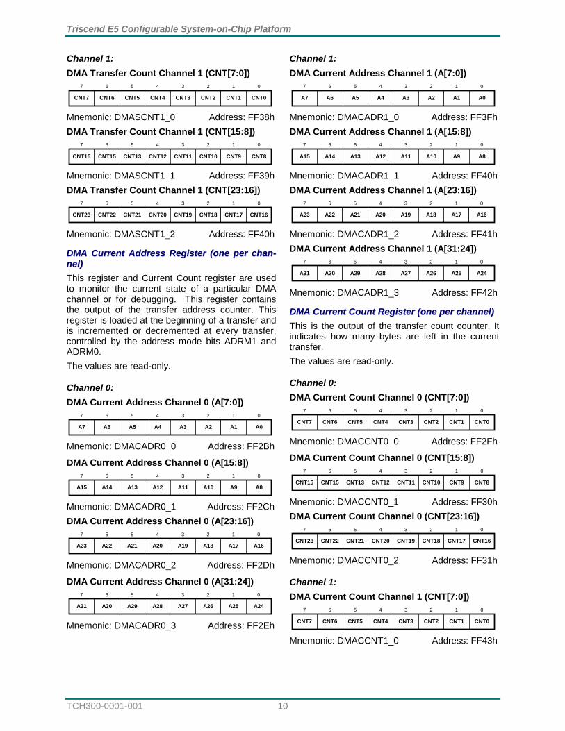
Channel 1: DMA Transfer Count Channel 1 (CNT[7:0])
CNT7 CNT6 CNT5 CNT4 CNT3 CNT2 CNT1 CNT0
7 6 5 4 3 2 1 0
Mnemonic: DMASCNT1_0 Address: FF38h DMA Transfer Count Channel 1 (CNT[15:8])
CNT15 CNT15 CNT13 CNT12 CNT11 CNT10 CNT9 CNT8
7 6 5 4 3 2 1 0
Mnemonic: DMASCNT1_1 Address: FF39h DMA Transfer Count Channel 1 (CNT[23:16])
CNT23 CNT22 CNT21 CNT20 CNT19 CNT18 CNT17 CNT16
7 6 5 4 3 2 1 0
Mnemonic: DMASCNT1_2 Address: FF40h
DDMMAA CCuurrrreenntt AAddddrreessss RReeggiisstteerr ((oonnee ppeerr cchhaann--nneell)) This register and Current Count register are used to monitor the current state of a particular DMA channel or for debugging. This register contains the output of the transfer address counter. This register is loaded at the beginning of a transfer and is incremented or decremented at every transfer, controlled by the address mode bits ADRM1 and ADRM0. The values are read-only.
Channel 0: DMA Current Address Channel 0 (A[7:0])
A7 A6 A5 A4 A3 A2 A1 A0
7 6 5 4 3 2 1 0
Mnemonic: DMACADR0_0 Address: FF2Bh
DMA Current Address Channel 0 (A[15:8])
A15 A14 A13 A12 A11 A10 A9 A8
7 6 5 4 3 2 1 0
Mnemonic: DMACADR0_1 Address: FF2Ch DMA Current Address Channel 0 (A[23:16])
A23 A22 A21 A20 A19 A18 A17 A16
7 6 5 4 3 2 1 0
Mnemonic: DMACADR0_2 Address: FF2Dh
DMA Current Address Channel 0 (A[31:24])
A31 A30 A29 A28 A27 A26 A25 A24
7 6 5 4 3 2 1 0
Mnemonic: DMACADR0_3 Address: FF2Eh
Channel 1: DMA Current Address Channel 1 (A[7:0])
A7 A6 A5 A4 A3 A2 A1 A0
7 6 5 4 3 2 1 0
Mnemonic: DMACADR1_0 Address: FF3Fh DMA Current Address Channel 1 (A[15:8])
A15 A14 A13 A12 A11 A10 A9 A8
7 6 5 4 3 2 1 0
Mnemonic: DMACADR1_1 Address: FF40h DMA Current Address Channel 1 (A[23:16])
A23 A22 A21 A20 A19 A18 A17 A16
7 6 5 4 3 2 1 0
Mnemonic: DMACADR1_2 Address: FF41h DMA Current Address Channel 1 (A[31:24])
A31 A30 A29 A28 A27 A26 A25 A24
7 6 5 4 3 2 1 0
Mnemonic: DMACADR1_3 Address: FF42h
DDMMAA CCuurrrreenntt CCoouunntt RReeggiisstteerr ((oonnee ppeerr cchhaannnneell)) This is the output of the transfer count counter. It indicates how many bytes are left in the current transfer. The values are read-only.
Channel 0: DMA Current Count Channel 0 (CNT[7:0])
CNT7 CNT6 CNT5 CNT4 CNT3 CNT2 CNT1 CNT0
7 6 5 4 3 2 1 0
Mnemonic: DMACCNT0_0 Address: FF2Fh
DMA Current Count Channel 0 (CNT[15:8])
CNT15 CNT15 CNT13 CNT12 CNT11 CNT10 CNT9 CNT8
7 6 5 4 3 2 1 0
Mnemonic: DMACCNT0_1 Address: FF30h DMA Current Count Channel 0 (CNT[23:16])
CNT23 CNT22 CNT21 CNT20 CNT19 CNT18 CNT17 CNT16
7 6 5 4 3 2 1 0
Mnemonic: DMACCNT0_2 Address: FF31h
Channel 1: DMA Current Count Channel 1 (CNT[7:0])
CNT7 CNT6 CNT5 CNT4 CNT3 CNT2 CNT1 CNT0
7 6 5 4 3 2 1 0
Mnemonic: DMACCNT1_0 Address: FF43h
11 TCH300-0001-001
DMA Current Count Channel 1 (CNT[15:8])
CNT15 CNT15 CNT13 CNT12 CNT11 CNT10 CNT9 CNT8
7 6 5 4 3 2 1 0
Mnemonic: DMACCNT1_1 Address: FF44h DMA Current Count Channel 1 (CNT[23:16])
CNT23 CNT22 CNT21 CNT20 CNT19 CNT18 CNT17 CNT16
7 6 5 4 3 2 1 0
Mnemonic: DMACCNT1_2 Address: FF45h
DDMMAA CCoonnttrrooll RReeggiisstteerr ((oonnee ppeerr cchhaannnneell)) Channel 0:
W/R- PAIR BLOCK SFTREQ CONT INIT EN CLR
7 6 5 4 3 2 1 0
Mnemonic: DMACTRL0_0 Address: FF27h
7 6 5 4 3 2 1 0
CRC_EN ADRM1 ADRM0Reserved
Mnemonic: DMACTRL0_1 Address: FF28h Channel 1:
W/R- PAIR BLOCK SFTREQ CONT INIT EN CLR
7 6 5 4 3 2 1 0
Mnemonic: DMACTRL1_0 Address: FF3Bh
7 6 5 4 3 2 1 0
CRC_EN ADRM1 ADRM0Reserved
Mnemonic: DMACTRL1_1 Address: FF3Ch All values are read/writeable. CLR, when set, disables the DMA channel and clears the transfer counter and pending requests counter. Clearing the bit indicates that the DMA channel is ready to operate. Cleared by reset. EN, when set, enables the DMA request for the channel. When this bit is set, the pending requests counter is cleared and the DMA channel is ready to accept requests. When this bit is cleared, incom-ing requests are ignored. Cleared by reset. INIT, when set, initializes a DMA transfer. An ini-tialization is associated with the transfer of each block transfer. When this bit is set, the starting operation values are loaded into their correspond-ing counters at the beginning of a transfer. Once the transfer has started, the bit is cleared by hard-ware. Software can set it again during the current block transfer to prepare the DMA channel for the next block. When cleared, the DMA stops after the current transfer. Cleared by reset. CONT, when set, indicates continuous initialization mode. When set, the DMA transfer on the current block continues until this bit is cleared. Cleared by reset.
SFTREQ, when set, requests a software-initiated DMA transfer. This bit is cleared by hardware on the following clock cycle. BLOCK, when set, indicates block request mode. When set, a complete block transfer is performed by the DMA upon receiving a single request from a device. Unaffected by reset. PAIR, when set in both channels, couples the two DMA channels to perform memory-to-memory transfers. Unaffected by reset. W/R- indicates the direction of the DMA transfer. When set, the DMA performs a memory-to-I/O transfer (DMA Write). When clear, the DMA per-forms an I/O-to-memory transfer (DMA Read). Unaffected by reset. ADRM1 and ADRM0 define the transfer address mode as shown below. Unaffected by reset.
Table 2. DMA Address Mode Settings. ADRM1 ADRM0 Mode
0 0 Increment address by one after each byte transfer
1 0 Decrement address by one after each byte transfer
x 1 Single address transfer (address remains constant)
CRC_EN enables CRC checking. When set, this bit activates the CRC logic. A 0-to-1 transition on this bit resets the CRC logic to 0. Cleared by a power-on reset or other device-wide reset.
DDMMAA PPeennddiinngg RReeqquueessttss ((oonnee ppeerr cchhaannnneell)) This field indicates the number of DMA requests yet to be serviced. Up to 64K requests can be re-ceived ahead of their corresponding acknowledge. Cleared by a power-on reset or other device-wide reset. The values are read-only.
Channel 0: DMA Pending Requests Channel 0 (REQ[7:0])
REQ7 REQ6 REQ5 REQ4 REQ3 REQ2 REQ1 REQ0
7 6 5 4 3 2 1 0
Mnemonic: DMAPREQ0_0 Address: FF32h DMA Pending Requests Channel 0 (REQ[15:8])
REQ15 REQ14 REQ13 REQ12 REQ11 REQ10 REQ9 REQ8
7 6 5 4 3 2 1 0
Mnemonic: DMAPREQ0_1 Address: FF33h
Triscend E5 Configurable System-on-Chip Platform
TCH300-0001-001 12
Channel 1: DMA Pending Requests Channel 1 (REQ[7:0])
REQ7 REQ6 REQ5 REQ4 REQ3 REQ2 REQ1 REQ0
7 6 5 4 3 2 1 0
Mnemonic: DMAPREQ1_0 Address: FF46h DMA Pending Requests Channel 1 (REQ[15:8])
REQ15 REQ14 REQ13 REQ12 REQ11 REQ10 REQ9 REQ8
7 6 5 4 3 2 1 0
Mnemonic: DMAPREQ1_1 Address: FF47h
DDMMAA IInntteerrrruupptt EEnnaabbllee RReeggiisstteerr ((oonnee ppeerr cchhaann--nneell)) The DMA interrupt register enables individual inter-rupt events for each channel. Channel 0:
Reserved OVR_EN INIT_EN TC_EN
7 6 5 4 3 2 1 0
Mnemonic: DMAEINT0 Address: FF29h Channel 1:
Reserved OVR_EN INIT_EN TC_EN
7 6 5 4 3 2 1 0
Mnemonic: DMAEINT1 Address: FF3Dh All values are read/writeable. TC_EN, when set, enables the DMA interrupt to indicate that the transfer counter reached its termi-nal count (TC). INIT_EN, when set, enables the DMA interrupt upon initialization. OVR_EN, when set, enables the DMA interrupt to indicate that the pending requests counter ex-ceeded 64K. Cleared by a power-on reset or other device-wide reset.
DDMMAA SSttaattuuss RReeggiisstteerr ((oonnee ppeerr cchhaannnneell)) Channel 0:
OVR INIT TC
7 6 5 4 3 2 1 0
Reserved
Mnemonic: DMAINT0 Address: FF2Ah Channel 1:
OVR INIT TC
7 6 5 4 3 2 1 0
Reserved
Mnemonic: DMAINT1 Address: FF3Eh TC, when set, indicates that the transfer counter reached terminal count. This bit is cleared when the INIT bit is set. This bit is set by hardware and is cleared by software by writing a one. Writing a
zero has no effect. Used in conjunction with TC_EN to flag an interrupt. INIT, when set, indicates that initialization has oc-curred. This bit is set by hardware and cleared by software by writing a one. Writing a zero has no effect. This bit is also cleared when software sets the INIT bit in the corresponding channel's DMA control register. Used in conjunction with INIT_EN to flag an interrupt. OVR, when set, indicates that the pending requests counter has overflowed. This bit is set by hardware and cleared by software by writing a one. Writing a zero has no effect. This bit is also cleared when the corresponding channel's pending requests counter is cleared. Used in conjunction with OVR_EN to flag an interrupt.
NOTE:
The OVR, INIT, and TC bits in the DMA Status Register are cleared by writing a ‘1’ to their respective bit location. Writ-ing a zero has no effect.
Cleared by a power-on reset or other device-wide reset.
DDMMAA UUnniitt CCRRCC OOuuttppuutt RReeggiisstteerr Once a transfer is completed, the output of the CRC register can be read by software, and the sig-nature can be compared with the expected value. DMA CRC Register (CRC[7:0])
CRC7 CRC6 CRC5 CRC4 CRC3 CRC2 CRC1 CRC0
7 6 5 4 3 2 1 0
Mnemonic: DMACRC_0 Address: FF48h
DMA CRC Register (CRC[15:8])
CRC15 CRC14 CRC13 CRC12 CRC11 CRC10 CRC9 CRC8
7 6 5 4 3 2 1 0
Mnemonic: DMACRC_1 Address: FF49h This register is shared by both DMA channels. Cleared by a power-on reset or other device-wide reset.
IInntteerrffaacciinngg CCSSLL PPeerriipphheerraallss ttoo tthhee DDMMAA CCoonn--ttrroolllleerr "Soft" modules implemented in the Configurable System Logic matrix have full access to DMA ser-vices. Access is provided via distributed DMA con-trol registers that steer DMA requests from periph-erals to the appropriate DMA channel and steer the appropriate DMA channel acknowledge signal back to the peripheral, as shown in Figure 5.
13 TCH300-0001-001
REQSEL
ConfigurableSystem Logic
DM
A C
ontr
ol R
egis
ter
ACKSEL
DMAChannel 1
Request
Acknowledge
DMAChannel 0
Request
Acknowledge
Figure 5. DMA Control Registers steer control
signals from CSL “soft” modules to the DMA channels.
DMA control registers share the same program-mable address selector functions also used for ad-dress decoding and chip selects. See Table 3 for the number of selectors available in each device. The address for a DMA control register is pro-grammable, similar to any function using a Selec-tor. A symbolic address name for the specific DMA control register is provided during design. The ac-tual address assignment is usually left to the Tris-cend FastChip development system. All DMA con-trol registers are single-byte registers and must be located within data or SFR memory spaces. An individual DMA control register controls a uni-directional DMA transfer, i.e., a memory-to-I/O (DMA write) or an I/O-to-memory (DMA read) transaction. However, a DMA control register is associated with a specific DMA channel by chang-ing the SEL bit within the control register. Two DMA control registers are required for DMA read and DMA write operations from the same periph-eral. A DMA control register is enabled for DMA access by setting the ENBL bits. Until enabled, all DMA requests (REQSEL) from a DMA control register are ignored. In standard use, only one DMA control register should be enabled per channel, per direction at any time, for a maximum of four. These four control registers cover individual DMA read and write op-erations from both channels 0 and 1. Another DMA control register can be enabled via software after first disabling the active control register.
DDiissttrriibbuutteedd DDMMAA CCoonnttrrooll RReeggiisstteerr
- - SEL ENBL - - SEL ENBL
7 6 5 4 3 2 1 0
Write both nibbles with duplicate data.Read register and OR bits from each nibble.
Mnemonic: User-Defined Address: User Defined Undefined bit locations are reserved and return 0 when read.
NOTE:
The distributed DMA Control registers only connect to either the high nibble or the low nibble of the CSI data bus. Con-sequently, application code should write duplicate copies of the high and low nib-ble. When reading, only the high or the low nibble will contain valid data. The high and low nibbles should be ORed together to determine the actual settings.
SEL steers control signals to and from the DMA controller. If SEL is cleared, the REQSEL input and ACKSEL output signals are steered to DMA channel 0. If SEL is set, then the signals are steered to DMA channel 1. The SEL control bit must be written to both bits 5 and 1. When read, both bits must be ORed together. ENBL, when set, allows the CSL “soft” module to access the DMA controller through the REQSEL input and ACKSEL output associated with DMA Control register. When ENBL is cleared, the DMA controller ignores any requests from the CSL mod-ule and the CSL module ignores any DMA ac-knowledges. The ENBL control bit must be written to both bits 4 and 0. When read, both bits must be ORed together. A DMA control register is reset to 00h by a reset. There is unrestricted read/write access to this reg-ister.
DDMMAA RReeqquueesstt SStteeeerriinngg To request a DMA transfer, the CSL “soft” module function asserts the REQSEL input on the DMA control register, as shown in Figure 6. If enabled (ENBL=1), the REQSEL signal is forwarded to ap-propriate DMA channel request, depending on the SEL value. If SEL=0, then REQSEL requests channel 0, else REQSEL requests channel 1. If disabled (ENBL=0), the request is blocked.
REQSEL
ENBLSEL
ConfigurableSystem Logic
DMA Select Register
DMA0 REQ
Request toDMA Controller
DMA1 REQ
Figure 6. A DMA Control Register steers DMA
requests to the appropriate channel.
DDMMAA AAcckknnoowwlleeddggee SStteeeerriinngg Once a “soft” module requests a DMA transfer, control over the transaction shifts to the DMA channel. The DMA channel requests the CSI bus. Once granted, the DMA channel asserts is ac-knowledge signal, which is steered back to the re-
Triscend E5 Configurable System-on-Chip Platform
TCH300-0001-001 14
questing CSL “soft” module via the ACKSEL out-put. The control logic is shown in Figure 7. When ACKSEL is asserted High, the CSL module should respond appropriately. During a DMA read (I/O-to-memory transfer), the CSL module should present data on the Data Read bus when ACKSEL is asserted. During a DMA write (memory-to-I/O transfer), the CSL module should accept the data on the Data Write bus when ACKSEL is asserted.
BUSCLK
D Q ACKSEL
ENBLSEL
1
0
ConfigurableSystem Logic
DMA Select Register
DMA1 ACK
DMA0 ACK
Acknowledge fromDMA Controller
Figure 7. DMA acknowledge signals are steered
back to the requesting CSL “soft” module.
The requesting device must be ready to accept the ACKSEL signal in a single cycle, since wait state capabilities are reserved strictly for memory-mapped operations. The DMA controller is de-signed to maximize bus bandwidth.
EExxaammppllee DDMMAA WWrriittee TTrraannssaaccttiioonn Figure 8 shows the waveform for a typical DMA write operation, i.e., a memory-to-I/O transfer. Prior to the first request, one of the DMA channels is configured for a DMA write operation and the proper values loaded into its configuration regis-ters. Likewise, a DMA control register—part of a CSL “soft” module function—is enabled (ENBL=1) and the channel select bit is set to steer signals to the proper DMA channel (SEL=0 for channel 0, SEL=1 for channel 1). The remainder of the transaction is as shown Figure 8. 1. The requesting “soft” module asserts its RE-
QSEL DMA request signal. Within the DMA control register, this incoming request is steered to the proper DMA channel.
2. The DMA channel requests the CSI bus from the bus arbiter. This process may require mul-tiple clock cycles.
3. Once the bus arbiter grants the bus to the DMA controller, the DMA presents the transfer ad-dress, the write data, and asserts its acknowl-edge signal. Within the DMA control register, the DMA channel's acknowledge signal is steered back to the requesting CSL “soft” module function. Consequently, the ACKSEL signal is asserted, signaling the “soft” module
that data is available. The “soft” module uses the ACKSEL signal to enable a register and capture the value presented on the Data Write bus.
Data Write[7:0]
AckSel
Bus Clock
ReqSel # $
%
DATA
Figure 8. Example DMA Write operation.
UUssiinngg tthhee DDMMAA CCoonnttrroolllleerr aass aa PPrrooxxyy BBuuss MMaass--tteerr “Soft” modules implemented in the CSL matrix are bus slaves, unable to request and control the bus by themselves. However, a CSL module can use the dedicated DMA controller as a "proxy" bus master. A bus master requires interaction with the bus arbi-ter, registers and counters to track addresses, and state machines to handle the bus transfer protocol. Such logic would consume CSL logic resources, if direct bus mastering were supported. A more effi-cient approach is to re-use the dedicated resources already built into the DMA controller. The DMA controller contains the logic to arbitrate for the bus, track address, and control transfers. A CSL “soft” module uses the DMA controller as a "proxy" master, causing the DMA controller to arbi-trate for and control the bus transaction.
15 TCH300-0001-001
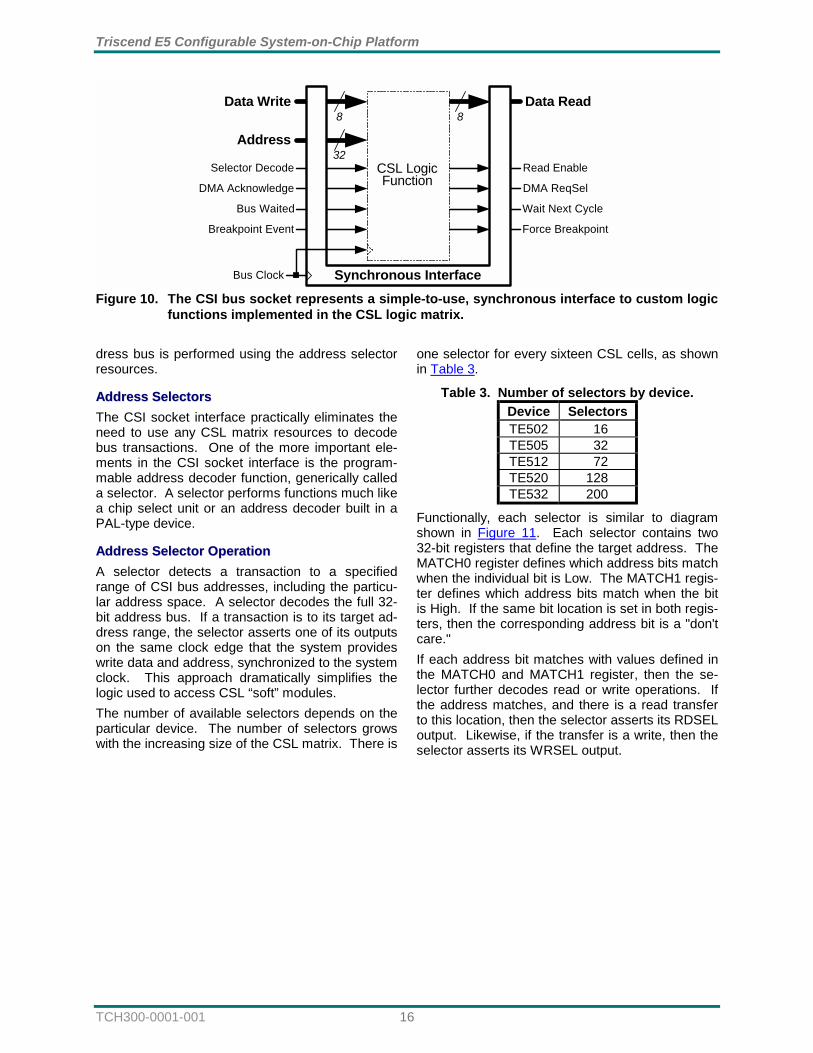
Configurable System Interconnect (CSI) Bus The Configurable System Interconnect (CSI) bus, shown in Figure 9, bridges the microcontroller to its peripherals and functions implemented in the Con-figurable System Logic (CSL) matrix. The CSI bus provides a processor-independent migration path to future generations of configurable system-on-chip devices. User-defined and library-provided “soft” modules can be moved to future Triscend configurable system-on-chip families with little or no modification The CSI bus socket provides a simple, synchro-nous interface to functions implemented in the CSL matrix, as shown in Figure 10. The CSI bus inter-face socket consists of the following signals.
! An 8-bit write data port
! An 8-bit read data port, including a read enable signal to enable the read data back onto the CSI system bus.
! A 32-bit address port.
! A set of address selector (chip select) functions. The number of selectors varies according to device size as shown in Table 3. The selectors optionally steer DMA request and acknowledge signals to and from the CSL matrix.
! The bus clock.
! Wait-state control and monitor signals.
! Hardware breakpoint control and monitor sig-nals.
DDaattaa RReeaadd BBuuss Data is presented to the 8-bit read bus when the selected CSL logic function or "soft" module as-serts its read enable signal. The read data values from all functions are logically OR-ed together. Consequently, all unselected CSL functions drive the read bus with zeroes. Only the selected func-tion presents ones. Read data can be presented during every active bus cycle.
DDaattaa WWrriittee BBuuss The eight data write bits are presented on the CSI socket. Write data may be presented during every active bus cycle.
AAddddrreessss BBuuss All 32 address bits are presented via the CSI inter-face socket. Typically, only a few, if any, of the address signals are used by functions in the CSL matrix. Typically, the actual decoding of the ad-
Data Write
Data Read
Bus Clock
BreakpointControl
Wait-StateControl
Address
Sele
ctor
s
Con
figur
able
Sys
tem
Log
ic (C
SL) M
atrix8032
"Turbo"Microcontroller
Side-band Signals
CSI Socket Interface
Con
figur
able
Sys
tem
Inte
rcon
nect
(CSI
) Bus
DMA Request/Acknowledge
2-ChannelDMA Controller
HardwareBreakpoint Unit
Figure 9. The Configurable System Interconnect (CSI) bus and the socket interface to "soft"
modules in the CSL matrix.
Triscend E5 Configurable System-on-Chip Platform
TCH300-0001-001 16
dress bus is performed using the address selector resources.
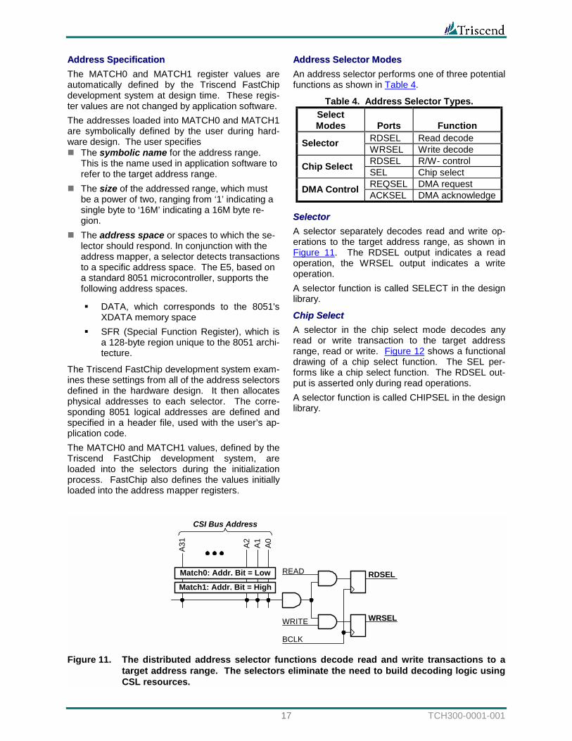
AAddddrreessss SSeelleeccttoorrss The CSI socket interface practically eliminates the need to use any CSL matrix resources to decode bus transactions. One of the more important ele-ments in the CSI socket interface is the program-mable address decoder function, generically called a selector. A selector performs functions much like a chip select unit or an address decoder built in a PAL-type device.
AAddddrreessss SSeelleeccttoorr OOppeerraattiioonn A selector detects a transaction to a specified range of CSI bus addresses, including the particu-lar address space. A selector decodes the full 32-bit address bus. If a transaction is to its target ad-dress range, the selector asserts one of its outputs on the same clock edge that the system provides write data and address, synchronized to the system clock. This approach dramatically simplifies the logic used to access CSL “soft” modules. The number of available selectors depends on the particular device. The number of selectors grows with the increasing size of the CSL matrix. There is
one selector for every sixteen CSL cells, as shown in Table 3.
Table 3. Number of selectors by device. Device Selectors TE502 16 TE505 32 TE512 72 TE520 128 TE532 200
Functionally, each selector is similar to diagram shown in Figure 11. Each selector contains two 32-bit registers that define the target address. The MATCH0 register defines which address bits match when the individual bit is Low. The MATCH1 regis-ter defines which address bits match when the bit is High. If the same bit location is set in both regis-ters, then the corresponding address bit is a "don't care." If each address bit matches with values defined in the MATCH0 and MATCH1 register, then the se-lector further decodes read or write operations. If the address matches, and there is a read transfer to this location, then the selector asserts its RDSEL output. Likewise, if the transfer is a write, then the selector asserts its WRSEL output.
DMA ReqSel
Wait Next Cycle
Force Breakpoint
8Data Read
Read Enable32
Address
Data Write8
Selector Decode
DMA Acknowledge
Bus Waited
Breakpoint Event
Bus Clock
CSL LogicFunction
Synchronous Interface
Figure 10. The CSI bus socket represents a simple-to-use, synchronous interface to custom logic functions implemented in the CSL logic matrix.
17 TCH300-0001-001
AAddddrreessss SSppeecciiffiiccaattiioonn The MATCH0 and MATCH1 register values are automatically defined by the Triscend FastChip development system at design time. These regis-ter values are not changed by application software. The addresses loaded into MATCH0 and MATCH1 are symbolically defined by the user during hard-ware design. The user specifies ! The symbolic name for the address range.
This is the name used in application software to refer to the target address range.
! The size of the addressed range, which must be a power of two, ranging from ‘1’ indicating a single byte to ‘16M’ indicating a 16M byte re-gion.
! The address space or spaces to which the se-lector should respond. In conjunction with the address mapper, a selector detects transactions to a specific address space. The E5, based on a standard 8051 microcontroller, supports the following address spaces.
& DATA, which corresponds to the 8051's XDATA memory space
& SFR (Special Function Register), which is a 128-byte region unique to the 8051 archi-tecture.
The Triscend FastChip development system exam-ines these settings from all of the address selectors defined in the hardware design. It then allocates physical addresses to each selector. The corre-sponding 8051 logical addresses are defined and specified in a header file, used with the user’s ap-plication code. The MATCH0 and MATCH1 values, defined by the Triscend FastChip development system, are loaded into the selectors during the initialization process. FastChip also defines the values initially loaded into the address mapper registers.
AAddddrreessss SSeelleeccttoorr MMooddeess An address selector performs one of three potential functions as shown in Table 4.
Table 4. Address Selector Types. Select Modes Ports Function
RDSEL Read decode Selector WRSEL Write decode RDSEL R/W- control Chip Select SEL Chip select REQSEL DMA request DMA Control ACKSEL DMA acknowledge
SSeelleeccttoorr A selector separately decodes read and write op-erations to the target address range, as shown in Figure 11. The RDSEL output indicates a read operation, the WRSEL output indicates a write operation. A selector function is called SELECT in the design library.
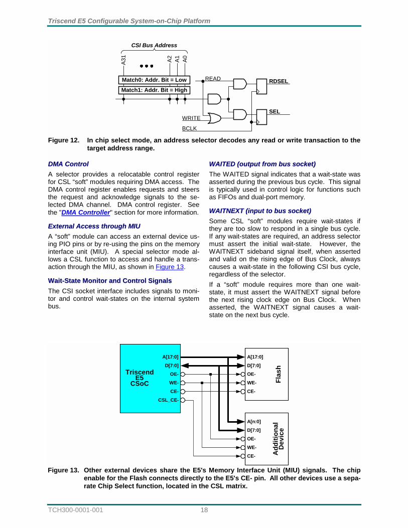
CChhiipp SSeelleecctt A selector in the chip select mode decodes any read or write transaction to the target address range, read or write. Figure 12 shows a functional drawing of a chip select function. The SEL per-forms like a chip select function. The RDSEL out-put is asserted only during read operations. A selector function is called CHIPSEL in the design library.
Match0: Addr. Bit = Low
Match1: Addr. Bit = High
A31
A0A1A2
CSI Bus Address
RDSEL
WRSEL
READ
WRITE
BCLK Figure 11. The distributed address selector functions decode read and write transactions to a
target address range. The selectors eliminate the need to build decoding logic using CSL resources.
Triscend E5 Configurable System-on-Chip Platform
TCH300-0001-001 18
DDMMAA CCoonnttrrooll A selector provides a relocatable control register for CSL “soft” modules requiring DMA access. The DMA control register enables requests and steers the request and acknowledge signals to the se-lected DMA channel. DMA control register. See the "DMA Controller" section for more information.
EExxtteerrnnaall AAcccceessss tthhrroouugghh MMIIUU A “soft” module can access an external device us-ing PIO pins or by re-using the pins on the memory interface unit (MIU). A special selector mode al-lows a CSL function to access and handle a trans-action through the MIU, as shown in Figure 13.
WWaaiitt--SSttaattee MMoonniittoorr aanndd CCoonnttrrooll SSiiggnnaallss The CSI socket interface includes signals to moni-tor and control wait-states on the internal system bus.
WWAAIITTEEDD ((oouuttppuutt ffrroomm bbuuss ssoocckkeett)) The WAITED signal indicates that a wait-state was asserted during the previous bus cycle. This signal is typically used in control logic for functions such as FIFOs and dual-port memory.
WWAAIITTNNEEXXTT ((iinnppuutt ttoo bbuuss ssoocckkeett)) Some CSL “soft” modules require wait-states if they are too slow to respond in a single bus cycle. If any wait-states are required, an address selector must assert the initial wait-state. However, the WAITNEXT sideband signal itself, when asserted and valid on the rising edge of Bus Clock, always causes a wait-state in the following CSI bus cycle, regardless of the selector. If a “soft” module requires more than one wait-state, it must assert the WAITNEXT signal before the next rising clock edge on Bus Clock. When asserted, the WAITNEXT signal causes a wait-state on the next bus cycle.
Match0: Addr. Bit = Low
Match1: Addr. Bit = High
A31
A0A1A2
CSI Bus Address
READ
BCLK
RDSEL
SELWRITE
Figure 12. In chip select mode, an address selector decodes any read or write transaction to the
target address range.
A[17:0]
D[7:0]
OE-
WE-
CE-
TriscendE5
CSoC
A[17:0]
Flas
hD[7:0]
OE-
WE-
CE-
A[n:0]
Add
ition
alD
evic
eD[7:0]
OE-
WE-
CE-
CSL_CE-
Figure 13. Other external devices share the E5's Memory Interface Unit (MIU) signals. The chip
enable for the Flash connects directly to the E5's CE- pin. All other devices use a sepa-rate Chip Select function, located in the CSL matrix.
19 TCH300-0001-001
IInniittiiaall WWaaiitt--SSttaattee IInnsseerrttiioonn Some “soft” modules implemented in the CSL ma-trix may require wait-states, either because the “soft” module handshakes with another asynchro-nous device or if the “soft” module is too slow to respond in a single bus cycle. If a “soft” module requires any wait-states, a selec-tor must assert the first wait-state. The selector will only assert a wait-state if the system is accessing the selector's target address space. Should a “soft” module require additional wait-states beyond the initial wait-state asserted by the selector, then the “soft” module indicates additional wait-states by asserting the WAITNEXT signal on the CSI socket interface.
BBrreeaakkppooiinntt EEvveenntt MMoonniittoorr aanndd CCoonnttrrooll SSiiggnnaallss The CSI socket interface includes signals to moni-tor and control hardware breakpoint events. These signals can be used to aid system-level debugging.
BBRREEAAKK ((iinnppuutt ttoo bbuuss ssoocckkeett)) CSL functions can force a hardware breakpoint event by asserting the BREAK signal. The hard-ware breakpoint unit typically only monitors trans-actions on the CSI bus. The BREAK signal allows CSL functions to interact with the hardware break-point unit. For example, a CSL function could be monitoring a serial communications stream that rarely interacts with the system bus. Upon detecting a particular pattern, the CSL function could force a breakpoint event, stopping the system. The state of the sys-tem or CSL functions could then be monitored through the JTAG port.
EEVVEENNTT ((oouuttppuutt ffrroomm bbuuss ssoocckkeett)) CSL functions can monitor hardware breakpoint events using the EVENT signal. When EVENT is asserted, a hardware breakpoint event has oc-curred, either caused by the hardware breakpoint event or by another function in the CSL matrix.
CCSSII BBuuss TTrraannssaaccttiioonnss The following section describes example CSI bus transactions, demonstrating the interaction of a CSL “soft” module and the CSI bus socket.
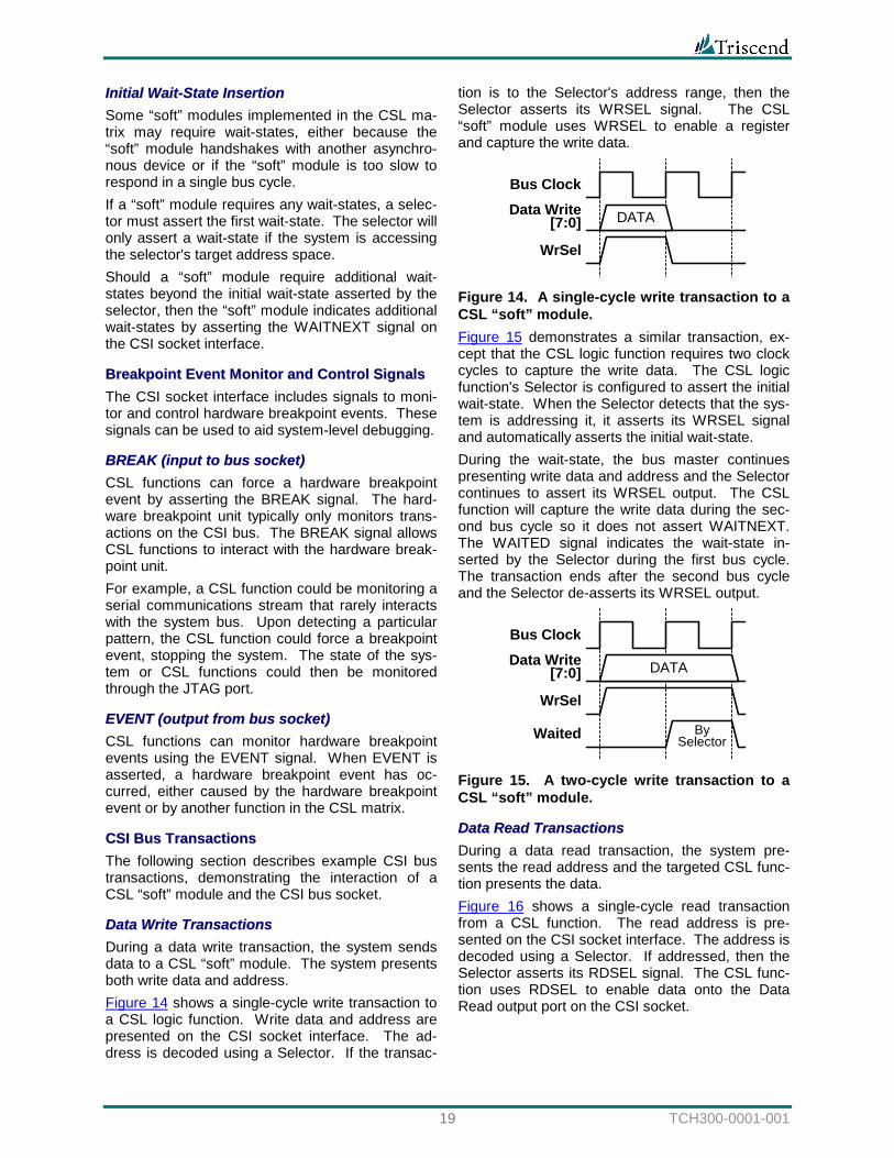
DDaattaa WWrriittee TTrraannssaaccttiioonnss During a data write transaction, the system sends data to a CSL “soft” module. The system presents both write data and address. Figure 14 shows a single-cycle write transaction to a CSL logic function. Write data and address are presented on the CSI socket interface. The ad-dress is decoded using a Selector. If the transac-
tion is to the Selector's address range, then the Selector asserts its WRSEL signal. The CSL “soft” module uses WRSEL to enable a register and capture the write data.
Bus Clock
WrSel
Data Write[7:0] DATA
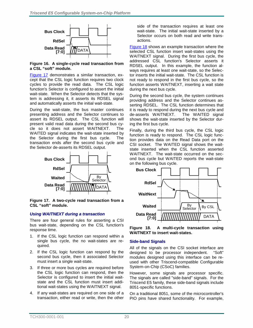
Figure 14. A single-cycle write transaction to a CSL “soft” module. Figure 15 demonstrates a similar transaction, ex-cept that the CSL logic function requires two clock cycles to capture the write data. The CSL logic function's Selector is configured to assert the initial wait-state. When the Selector detects that the sys-tem is addressing it, it asserts its WRSEL signal and automatically asserts the initial wait-state. During the wait-state, the bus master continues presenting write data and address and the Selector continues to assert its WRSEL output. The CSL function will capture the write data during the sec-ond bus cycle so it does not assert WAITNEXT. The WAITED signal indicates the wait-state in-serted by the Selector during the first bus cycle. The transaction ends after the second bus cycle and the Selector de-asserts its WRSEL output.
Bus Clock
Waited BySelector
WrSel
DATAData Write[7:0]
Figure 15. A two-cycle write transaction to a CSL “soft” module.
DDaattaa RReeaadd TTrraannssaaccttiioonnss During a data read transaction, the system pre-sents the read address and the targeted CSL func-tion presents the data. Figure 16 shows a single-cycle read transaction from a CSL function. The read address is pre-sented on the CSI socket interface. The address is decoded using a Selector. If addressed, then the Selector asserts its RDSEL signal. The CSL func-tion uses RDSEL to enable data onto the Data Read output port on the CSI socket.
Triscend E5 Configurable System-on-Chip Platform
TCH300-0001-001 20
Bus Clock
RdSel
DATAData Read[7:0]
Figure 16. A single-cycle read transaction from a CSL “soft” module. Figure 17 demonstrates a similar transaction, ex-cept that the CSL logic function requires two clock cycles to provide the read data. The CSL logic function's Selector is configured to assert the initial wait-state. When the Selector detects that the sys-tem is addressing it, it asserts its RDSEL signal and automatically asserts the initial wait-state. During the wait-state, the bus master continues presenting address and the Selector continues to assert its RDSEL output. The CSL function will present valid read data during the second bus cy-cle so it does not assert WAITNEXT. The WAITED signal indicates the wait-state inserted by the Selector during the first bus cycle. The transaction ends after the second bus cycle and the Selector de-asserts its RDSEL output.
Bus Clock
Waited BySelector
RdSel
DATAData Read[7:0]
Figure 17. A two-cycle read transaction from a CSL “soft” module.
UUssiinngg WWAAIITTNNEEXXTT dduurriinngg aa ttrraannssaaccttiioonn There are four general rules for asserting a CSI bus wait-state, depending on the CSL function's response time. 1. If the CSL logic function can respond within a
single bus cycle, the no wait-states are re-quired.
2. If the CSL logic function can respond by the second bus cycle, then it associated Selector must insert a single wait-state.
3. If three or more bus cycles are required before the CSL logic function can respond, then the Selector is configured to insert the initial wait-state and the CSL function must insert addi-tional wait-states using the WAITNEXT signal.
4. If any wait-states are required on one side of a transaction, either read or write, then the other
side of the transaction requires at least one wait-state. The initial wait-state inserted by a Selector occurs on both read and write trans-actions.
Figure 18 shows an example transaction where the selected CSL function insert wait-states using the WAITNEXT signal. During the first bus cycle, the addressed CSL function's Selector asserts it RDSEL output. In this example, the function al-ways requires at least one wait-state, so the Selec-tor inserts the initial wait-state. The CSL function is not ready to respond in the first bus cycle, so the function asserts WAITNEXT, inserting a wait state during the next bus cycle. During the second bus cycle, the system continues providing address and the Selector continues as-serting RDSEL. The CSL function determines that it is ready to respond during the next bus cycle and de-asserts WAITNEXT. The WAITED signal shows the wait-state inserted by the Selector dur-ing the first bus cycle. Finally, during the third bus cycle, the CSL logic function is ready to respond. The CSL logic func-tion provides data on the Read Data port on the CSI socket. The WAITED signal shows the wait-state inserted when the CSL function asserted WAITNEXT. The wait-state occurred on the sec-ond bus cycle but WAITED reports the wait-state on the following bus cycle.
Bus Clock
RdSel
Waited BySelector By CSL
WaitNext
DATAData Read[7:0]
Figure 18. A multi-cycle transaction using WAITNEXT to insert wait-states.
SSiiddee--bbaanndd SSiiggnnaallss All of the signals on the CSI socket interface are designed to be processor independent. “Soft” modules designed using this interface can be re-used with other Triscend-compatible Configurable System-on-Chip (CSoC) families. However, some signals are processor specific. The signals are called "side-band" signals. For the Triscend E5 family, these side-band signals include 8051-specific functions. On a traditional 8051, some of the microcontroller's PIO pins have shared functionality. For example,
21 TCH300-0001-001
the Timer 0 External Input, T0, typically shares a PIO pin on Port 3 (P3.4). On the E5, however, these processor-specific signals can connect to any PIO pin and even to functions implemented entirely within the Configurable System Logic (CSL) matrix. The side-band signals for the E5 CSoC device family are shown in Table 5. Refer to Sideband Signal Timing Characteristics for specific timing requirements.
Table 5. E5 Family Side-band Signals. E5 Function 8051 Signal
Timer 0 external input T0 Timer 1 external input T1 External I/O for Timer 2 T2 Timer/Counter 2 capture/reload trigger or an additional external interrupt source if Timer 2 baud-rate generator unused
T2EX
External Interrupt 0 INTR0 External Interrupt 1 INTR1 High-Priority Interrupt HPINT Serial port receive data input. Used in modes 1, 2, and 3. RXDIN
Serial port receiver output. Used in serial port mode 0 for shift clock.
RXDOUT
Serial port transmit data TXD Application reset from CSL ma-trix (RSTC), inverted polarity from the original 8051
RST-
Signal from the 8051 to the CSL matrix (CPURST). Indicates that the 8051 was reset for any reason, including the watchdog timer.
(no 8051 equivalent
signal)
Output of the crystal oscillator amplifier, distributed only to CSL functions.
XTAL
Triscend E5 Configurable System-on-Chip Platform
TCH300-0001-001 22
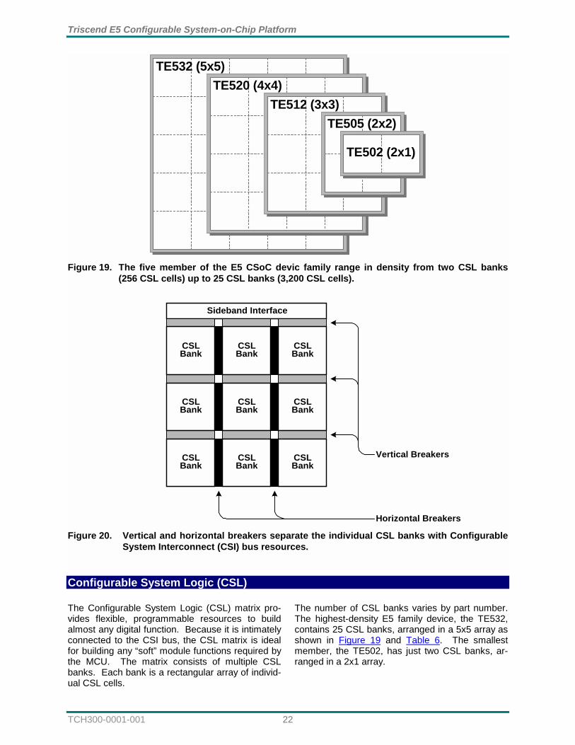
Configurable System Logic (CSL) The Configurable System Logic (CSL) matrix pro-vides flexible, programmable resources to build almost any digital function. Because it is intimately connected to the CSI bus, the CSL matrix is ideal for building any “soft” module functions required by the MCU. The matrix consists of multiple CSL banks. Each bank is a rectangular array of individ-ual CSL cells.
The number of CSL banks varies by part number. The highest-density E5 family device, the TE532, contains 25 CSL banks, arranged in a 5x5 array as shown in Figure 19 and Table 6. The smallest member, the TE502, has just two CSL banks, ar-ranged in a 2x1 array.
TE505 (2x2)TE512 (3x3)
TE520 (4x4)TE532 (5x5)
TE502 (2x1)
Figure 19. The five member of the E5 CSoC devic family range in density from two CSL banks
(256 CSL cells) up to 25 CSL banks (3,200 CSL cells).
Sideband Interface
CSLBank
CSLBank
CSLBank
CSLBank
CSLBank
CSLBank
CSLBank
CSLBank
CSLBank
Vertical Breakers
Horizontal Breakers Figure 20. Vertical and horizontal breakers separate the individual CSL banks with Configurable
System Interconnect (CSI) bus resources.
23 TCH300-0001-001
Table 6. CSL Banks by Device. CSL Banks Part
Number Columns Rows Total Total Cells
TE502 2 1 2 256 TE505 2 2 4 512 TE512 3 3 9 1,152 TE520 4 4 16 2,048 TE532 5 5 25 3,200
Vertical and horizontal breakers separate the indi-vidual CSL banks on a device, as shown in Figure 20. Vertical breakers appear at the top of every CSL bank. Horizontal breakers appear between adjacent columns of CSL banks. The breakers contain Configurable System Interconnect (CSI) bus resources. The horizontal breakers distribute CSI bus address signals to the CSL banks. The vertical breakers distribute the Selector input and output signals, breakpoint control signals, the global buffer signals, and the wait-state control sig-nals. The CSI read data return path is also located in the vertical breakers.
Signals from one CSL bank can cross into other banks via the breakers, though crossing a breaker adds delay to the signal. Sideband signals originate and terminate in re-sources along the top edge of the device.
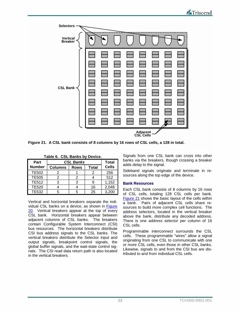
BBaannkk RReessoouurrcceess Each CSL bank consists of 8 columns by 16 rows of CSL cells, totaling 128 CSL cells per bank. Figure 21 shows the basic layout of the cells within a bank. Pairs of adjacent CSL cells share re-sources to build more complex cell functions. The address selectors, located in the vertical breaker above the bank, distribute any decoded address. There is one address selector per column of 16 CSL cells. Programmable interconnect surrounds the CSL cells. These programmable "wires" allow a signal originating from one CSL to communicate with one or more CSL cells, even those in other CSL banks. Likewise, signals to and from the CSI bus are dis-tributed to and from individual CSL cells.
CSL Bank
Selectors
VerticalBreaker
AdjacentCSL Cells
Figure 21. A CSL bank consists of 8 columns by 16 rows of CSL cells, a 128 in total.
Triscend E5 Configurable System-on-Chip Platform
TCH300-0001-001 24
RoutingMatrix
RoutingMatrix
RoutingMatrix
RoutingMatrix
CSL Cell
CSL Cell
8 Short Segments
8 Short Segments
8 Sh
ort S
egm
ents
8 Sh
ort S
egm
ents
8 Lo
ng L
ines
4 C
lock
/Glo
bal B
uffe
rs
4 C
lock
/Glo
bal B
uffe
rs
8 Lo
ng L
ines
4 Clock/Global Buffer
8 Long Lines
Selector outputsfrom vertical breaker
Selector outputsfrom vertical breaker
Addr
ess
outp
uts
from
hor
izon
tal b
reak
er
Carry,cascadedwide functionpath
Carry,cascadedwide functionpath
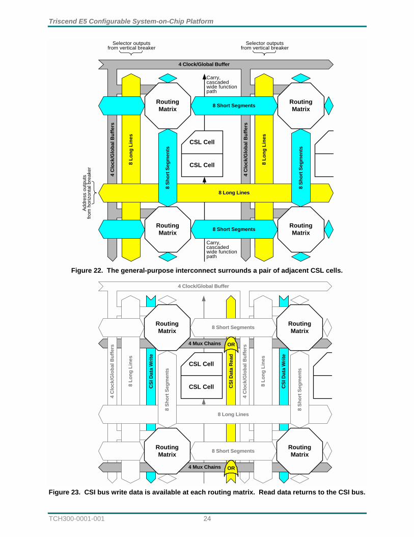
Figure 22. The general-purpose interconnect surrounds a pair of adjacent CSL cells.
RoutingMatrix
RoutingMatrix
RoutingMatrix
RoutingMatrix
CSL Cell
CSL Cell
8 Short Segments
8 Short Segments
8 Sh
ort S
egm
ents
8 Sh
ort S
egm
ents
8 Lo
ng L
ines
4 C
lock
/Glo
bal B
uffe
rs
4 C
lock
/Glo
bal B
uffe
rs
8 Lo
ng L
ines
CSI
Dat
a W
rite
CSI
Dat
a W
rite
4 Clock/Global Buffer
OR
OR
CSI
Dat
a R
ead
8 Long Lines
4 Mux Chains
4 Mux Chains
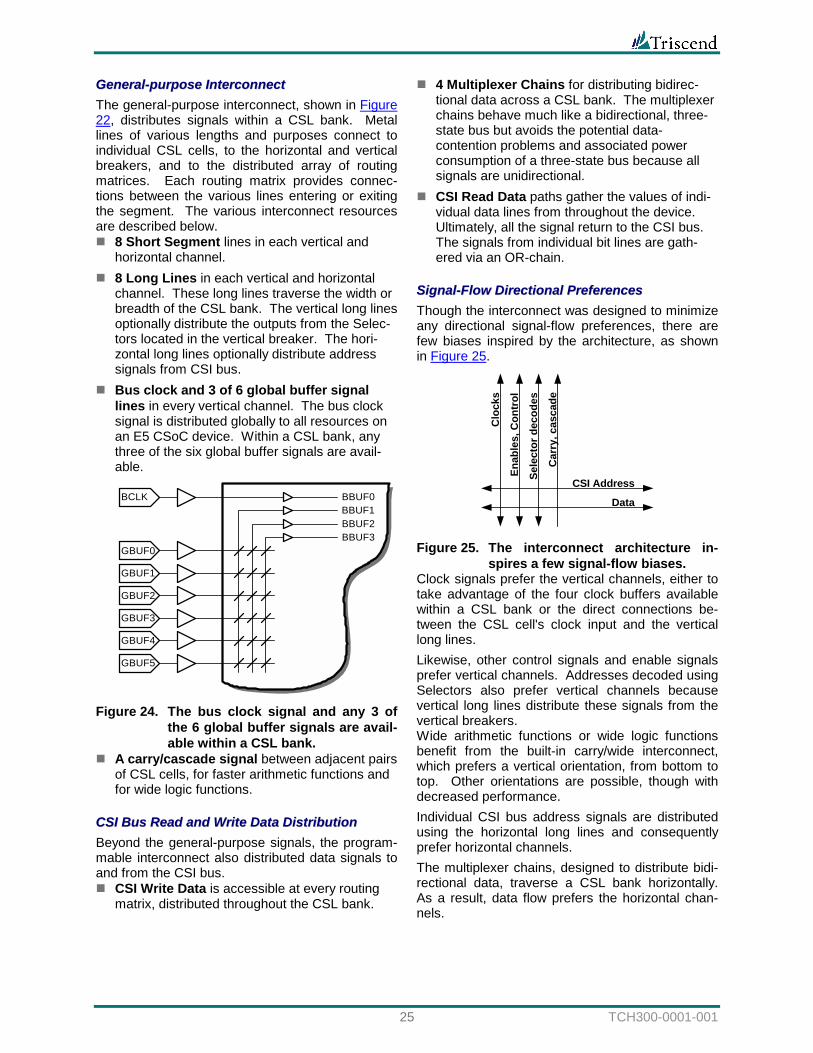
Figure 23. CSI bus write data is available at each routing matrix. Read data returns to the CSI bus.
25 TCH300-0001-001
GGeenneerraall--ppuurrppoossee IInntteerrccoonnnneecctt The general-purpose interconnect, shown in Figure 22, distributes signals within a CSL bank. Metal lines of various lengths and purposes connect to individual CSL cells, to the horizontal and vertical breakers, and to the distributed array of routing matrices. Each routing matrix provides connec-tions between the various lines entering or exiting the segment. The various interconnect resources are described below. ! 8 Short Segment lines in each vertical and
horizontal channel. ! 8 Long Lines in each vertical and horizontal
channel. These long lines traverse the width or breadth of the CSL bank. The vertical long lines optionally distribute the outputs from the Selec-tors located in the vertical breaker. The hori-zontal long lines optionally distribute address signals from CSI bus.
! Bus clock and 3 of 6 global buffer signal lines in every vertical channel. The bus clock signal is distributed globally to all resources on an E5 CSoC device. Within a CSL bank, any three of the six global buffer signals are avail-able.
BBUF0BCLKBBUF1BBUF2BBUF3
GBUF0
GBUF1
GBUF2
GBUF3
GBUF4
GBUF5
Figure 24. The bus clock signal and any 3 of
the 6 global buffer signals are avail-able within a CSL bank.
! A carry/cascade signal between adjacent pairs of CSL cells, for faster arithmetic functions and for wide logic functions.
CCSSII BBuuss RReeaadd aanndd WWrriittee DDaattaa DDiissttrriibbuuttiioonn Beyond the general-purpose signals, the program-mable interconnect also distributed data signals to and from the CSI bus. ! CSI Write Data is accessible at every routing
matrix, distributed throughout the CSL bank.
! 4 Multiplexer Chains for distributing bidirec-tional data across a CSL bank. The multiplexer chains behave much like a bidirectional, three-state bus but avoids the potential data-contention problems and associated power consumption of a three-state bus because all signals are unidirectional.
! CSI Read Data paths gather the values of indi-vidual data lines from throughout the device. Ultimately, all the signal return to the CSI bus. The signals from individual bit lines are gath-ered via an OR-chain.
SSiiggnnaall--FFllooww DDiirreeccttiioonnaall PPrreeffeerreenncceess Though the interconnect was designed to minimize any directional signal-flow preferences, there are few biases inspired by the architecture, as shown in Figure 25.
Enab
les,
Con
trol
Car
ry, c
asca
de
Clo
cks
Sele
ctor
dec
odes
Data
CSI Address
Figure 25. The interconnect architecture in-
spires a few signal-flow biases. Clock signals prefer the vertical channels, either to take advantage of the four clock buffers available within a CSL bank or the direct connections be-tween the CSL cell's clock input and the vertical long lines. Likewise, other control signals and enable signals prefer vertical channels. Addresses decoded using Selectors also prefer vertical channels because vertical long lines distribute these signals from the vertical breakers. Wide arithmetic functions or wide logic functions benefit from the built-in carry/wide interconnect, which prefers a vertical orientation, from bottom to top. Other orientations are possible, though with decreased performance. Individual CSI bus address signals are distributed using the horizontal long lines and consequently prefer horizontal channels. The multiplexer chains, designed to distribute bidi-rectional data, traverse a CSL bank horizontally. As a result, data flow prefers the horizontal chan-nels.
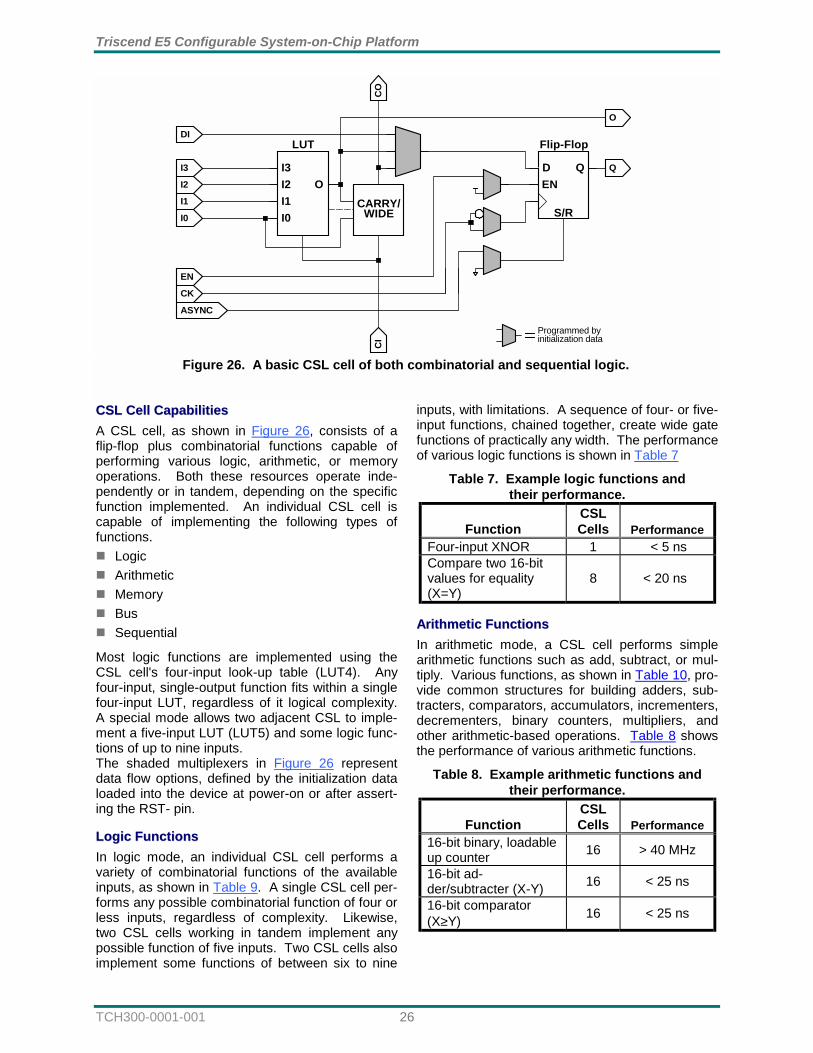
Triscend E5 Configurable System-on-Chip Platform
TCH300-0001-001 26
CCSSLL CCeellll CCaappaabbiilliittiieess A CSL cell, as shown in Figure 26, consists of a flip-flop plus combinatorial functions capable of performing various logic, arithmetic, or memory operations. Both these resources operate inde-pendently or in tandem, depending on the specific function implemented. An individual CSL cell is capable of implementing the following types of functions. ! Logic ! Arithmetic ! Memory ! Bus ! Sequential
Most logic functions are implemented using the CSL cell's four-input look-up table (LUT4). Any four-input, single-output function fits within a single four-input LUT, regardless of it logical complexity. A special mode allows two adjacent CSL to imple-ment a five-input LUT (LUT5) and some logic func-tions of up to nine inputs. The shaded multiplexers in Figure 26 represent data flow options, defined by the initialization data loaded into the device at power-on or after assert-ing the RST- pin.
LLooggiicc FFuunnccttiioonnss In logic mode, an individual CSL cell performs a variety of combinatorial functions of the available inputs, as shown in Table 9. A single CSL cell per-forms any possible combinatorial function of four or less inputs, regardless of complexity. Likewise, two CSL cells working in tandem implement any possible function of five inputs. Two CSL cells also implement some functions of between six to nine
inputs, with limitations. A sequence of four- or five-input functions, chained together, create wide gate functions of practically any width. The performance of various logic functions is shown in Table 7
Table 7. Example logic functions and their performance.
Function CSL Cells Performance
Four-input XNOR 1 < 5 ns Compare two 16-bit values for equality (X=Y)
8 < 20 ns
AArriitthhmmeettiicc FFuunnccttiioonnss In arithmetic mode, a CSL cell performs simple arithmetic functions such as add, subtract, or mul-tiply. Various functions, as shown in Table 10, pro-vide common structures for building adders, sub-tracters, comparators, accumulators, incrementers, decrementers, binary counters, multipliers, and other arithmetic-based operations. Table 8 shows the performance of various arithmetic functions.
Table 8. Example arithmetic functions and their performance.
Function CSL Cells Performance
16-bit binary, loadable up counter 16 > 40 MHz
16-bit ad-der/subtracter (X-Y) 16 < 25 ns
16-bit comparator (X≥Y) 16 < 25 ns
CARRY/WIDE
DEN
Q
S/R
Q
CI
DI
I3
I2
I1
I0
EN
CK
O
I3I2I1I0
O
CO
ASYNC
LUT Flip-Flop
Programmed byinitialization data
Figure 26. A basic CSL cell of both combinatorial and sequential logic.
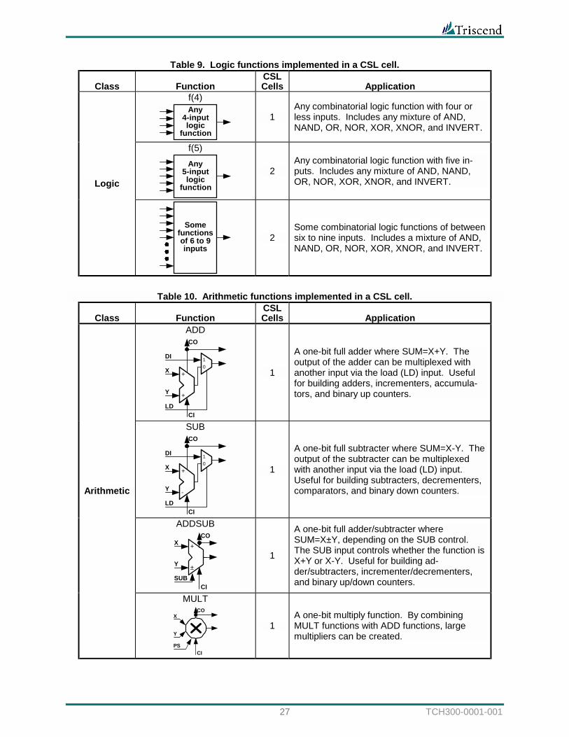
27 TCH300-0001-001
Table 9. Logic functions implemented in a CSL cell.
Class Function CSL Cells Application
f(4) Any
4-inputlogic
function
1 Any combinatorial logic function with four or less inputs. Includes any mixture of AND, NAND, OR, NOR, XOR, XNOR, and INVERT.
f(5) Any
5-inputlogic
function
2 Any combinatorial logic function with five in-puts. Includes any mixture of AND, NAND, OR, NOR, XOR, XNOR, and INVERT. Logic
Somefunctionsof 6 to 9inputs
2 Some combinatorial logic functions of between six to nine inputs. Includes a mixture of AND, NAND, OR, NOR, XOR, XNOR, and INVERT.
Table 10. Arithmetic functions implemented in a CSL cell.
Class Function CSL Cells Application
ADD
10
+
+X
Y
LD
DI
CI
CO
1
A one-bit full adder where SUM=X+Y. The output of the adder can be multiplexed with another input via the load (LD) input. Useful for building adders, incrementers, accumula-tors, and binary up counters.
SUB
10
-
+
CO
CILD
Y
X
DI
1
A one-bit full subtracter where SUM=X-Y. The output of the subtracter can be multiplexed with another input via the load (LD) input. Useful for building subtracters, decrementers, comparators, and binary down counters.
ADDSUB
±
+CO
CISUB
Y
X
1
A one-bit full adder/subtracter where SUM=X±Y, depending on the SUB control. The SUB input controls whether the function is X+Y or X-Y. Useful for building ad-der/subtracters, incrementer/decrementers, and binary up/down counters.
Arithmetic
MULT CO
CI
X
Y
PS
1 A one-bit multiply function. By combining MULT functions with ADD functions, large multipliers can be created.
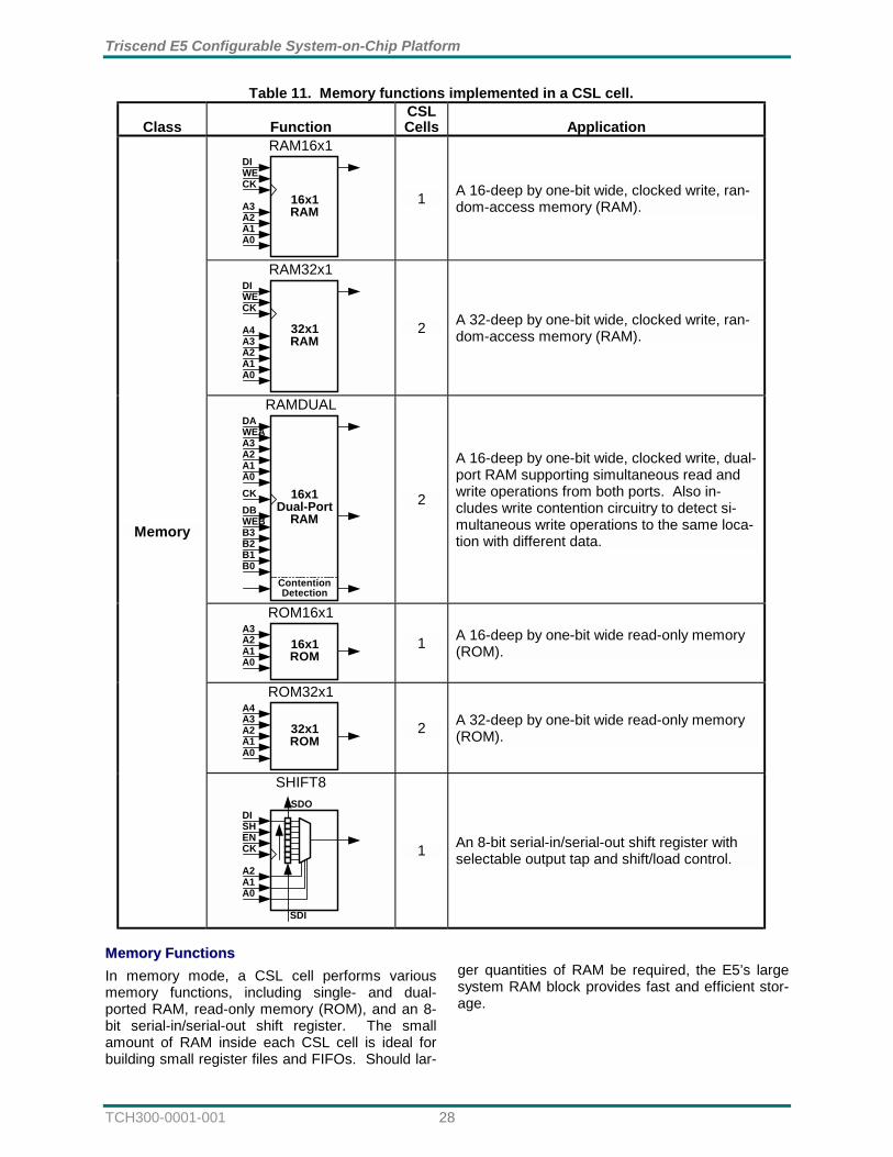
Triscend E5 Configurable System-on-Chip Platform
TCH300-0001-001 28
MMeemmoorryy FFuunnccttiioonnss In memory mode, a CSL cell performs various memory functions, including single- and dual-ported RAM, read-only memory (ROM), and an 8-bit serial-in/serial-out shift register. The small amount of RAM inside each CSL cell is ideal for building small register files and FIFOs. Should lar-
ger quantities of RAM be required, the E5’s large system RAM block provides fast and efficient stor-age.
Table 11. Memory functions implemented in a CSL cell.
Class Function CSL Cells Application
RAM16x1
16x1RAMA3
A2A1A0
DIWECK
1 A 16-deep by one-bit wide, clocked write, ran-dom-access memory (RAM).
RAM32x1
32x1RAM
A4A3A2A1A0
DIWECK
2 A 32-deep by one-bit wide, clocked write, ran-dom-access memory (RAM).
RAMDUAL
16x1Dual-Port
RAM
CK
A3A2A1A0
DAWEA
WEBB3B2B1B0
DB
ContentionDetection
2
A 16-deep by one-bit wide, clocked write, dual-port RAM supporting simultaneous read and write operations from both ports. Also in-cludes write contention circuitry to detect si-multaneous write operations to the same loca-tion with different data.
ROM16x1
16x1ROM
A3A2A1A0
1 A 16-deep by one-bit wide read-only memory (ROM).
ROM32x1
32x1ROM
A4A3A2A1A0
2 A 32-deep by one-bit wide read-only memory (ROM).
Memory
SHIFT8
EN
A2A1A0
DISH
CK
SDI
SDO
1 An 8-bit serial-in/serial-out shift register with selectable output tap and shift/load control.
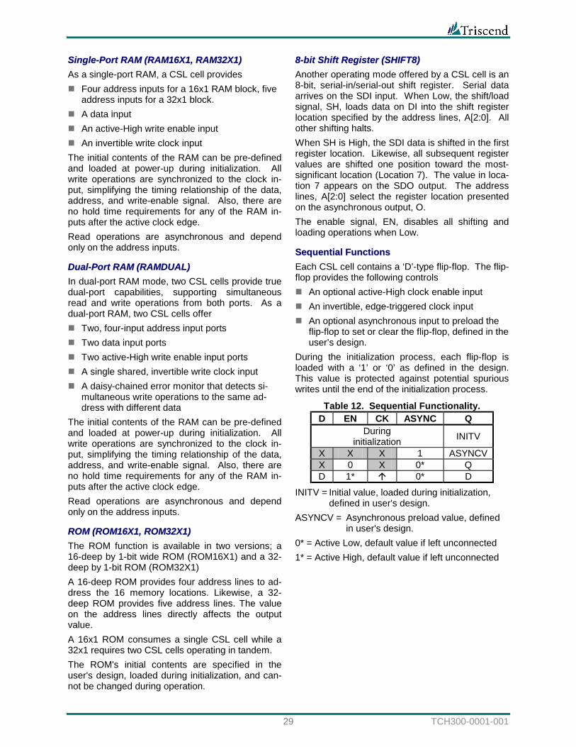
29 TCH300-0001-001
SSiinnggllee--PPoorrtt RRAAMM ((RRAAMM1166XX11,, RRAAMM3322XX11)) As a single-port RAM, a CSL cell provides ! Four address inputs for a 16x1 RAM block, five
address inputs for a 32x1 block. ! A data input ! An active-High write enable input ! An invertible write clock input The initial contents of the RAM can be pre-defined and loaded at power-up during initialization. All write operations are synchronized to the clock in-put, simplifying the timing relationship of the data, address, and write-enable signal. Also, there are no hold time requirements for any of the RAM in-puts after the active clock edge. Read operations are asynchronous and depend only on the address inputs.
DDuuaall--PPoorrtt RRAAMM ((RRAAMMDDUUAALL)) In dual-port RAM mode, two CSL cells provide true dual-port capabilities, supporting simultaneous read and write operations from both ports. As a dual-port RAM, two CSL cells offer ! Two, four-input address input ports ! Two data input ports ! Two active-High write enable input ports ! A single shared, invertible write clock input ! A daisy-chained error monitor that detects si-
multaneous write operations to the same ad-dress with different data
The initial contents of the RAM can be pre-defined and loaded at power-up during initialization. All write operations are synchronized to the clock in-put, simplifying the timing relationship of the data, address, and write-enable signal. Also, there are no hold time requirements for any of the RAM in-puts after the active clock edge. Read operations are asynchronous and depend only on the address inputs.
RROOMM ((RROOMM1166XX11,, RROOMM3322XX11)) The ROM function is available in two versions; a 16-deep by 1-bit wide ROM (ROM16X1) and a 32-deep by 1-bit ROM (ROM32X1) A 16-deep ROM provides four address lines to ad-dress the 16 memory locations. Likewise, a 32-deep ROM provides five address lines. The value on the address lines directly affects the output value. A 16x1 ROM consumes a single CSL cell while a 32x1 requires two CSL cells operating in tandem. The ROM's initial contents are specified in the user's design, loaded during initialization, and can-not be changed during operation.
88--bbiitt SShhiifftt RReeggiisstteerr ((SSHHIIFFTT88)) Another operating mode offered by a CSL cell is an 8-bit, serial-in/serial-out shift register. Serial data arrives on the SDI input. When Low, the shift/load signal, SH, loads data on DI into the shift register location specified by the address lines, A[2:0]. All other shifting halts. When SH is High, the SDI data is shifted in the first register location. Likewise, all subsequent register values are shifted one position toward the most-significant location (Location 7). The value in loca-tion 7 appears on the SDO output. The address lines, A[2:0] select the register location presented on the asynchronous output, O. The enable signal, EN, disables all shifting and loading operations when Low.
SSeeqquueennttiiaall FFuunnccttiioonnss Each CSL cell contains a ‘D’-type flip-flop. The flip-flop provides the following controls ! An optional active-High clock enable input ! An invertible, edge-triggered clock input ! An optional asynchronous input to preload the
flip-flop to set or clear the flip-flop, defined in the user’s design.
During the initialization process, each flip-flop is loaded with a ‘1’ or ‘0’ as defined in the design. This value is protected against potential spurious writes until the end of the initialization process.
Table 12. Sequential Functionality. D EN CK ASYNC Q
During initialization INITV
X X X 1 ASYNCV X 0 X 0* Q D 1* ' 0* D
INITV = Initial value, loaded during initialization, defined in user's design.
ASYNCV = Asynchronous preload value, defined in user's design.
0* = Active Low, default value if left unconnected 1* = Active High, default value if left unconnected
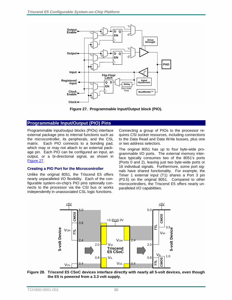
Triscend E5 Configurable System-on-Chip Platform
TCH300-0001-001 30
Programmable Input/Output (PIO) Pins Programmable input/output blocks (PIOs) interface external package pins to internal functions such as the microcontroller, its peripherals, and the CSL matrix. Each PIO connects to a bonding pad, which may or may not attach to an external pack-age pin. Each PIO can be configured an input, an output, or a bi-directional signal, as shown in Figure 27.
CCrreeaattiinngg aa PPIIOO PPoorrtt ffoorr tthhee MMiiccrrooccoonnttrroolllleerr Unlike the original 8051, the Triscend E5 offers nearly unparalleled I/O flexibility. Each of the con-figurable system-on-chip's PIO pins optionally con-nects to the processor via the CSI bus or works independently in unassociated CSL logic functions.
Connecting a group of PIOs to the processor re-quires CSI socket resources, including connections to the Data Read and Data Write busses, plus one or two address selectors. The original 8051 has up to four byte-wide pro-grammable I/O ports. The external memory inter-face typically consumes two of the 8051's ports (Ports 0 and 2), leaving just two byte-wide ports or 16 individual signals. Furthermore, some port sig-nals have shared functionality. For example, the Timer 1 external input (T1) shares a Port 3 pin (P3.5) on the original 8051. Compared to other microcontrollers, the Triscend E5 offers nearly un-paralleled I/O capabilities.
QEN
D
Flip-Flop/Latch
Input
RegisteredInput
Clock
ClockEnable
InputHysteresis
PAD
BusMinder™
OutputEnable
DriveStrength
Output
DelayZero Hold
Time
DEN
Q
DEN
Q
Figure 27. Programmable Input/Output block (PIO).
CM
OS
TTLVOH
VOL
0.8
2.4
3.8
5.0
2.0
VIL
VIH
0.4 0.4
2.4VOH
VOL
0.8 1.0
TTL
TTL
2.0
5.0
CM
OS
VIL
VIH
3.5
CM
OS
TriscendE5 CSoC
+3.3V±0.3V
+5V +5V
5-vo
lt D
evic
e
5-vo
lt D
evic
e
Figure 28. Triscend E5 CSoC devices interface directly with nearly all 5-volt devices, even though
the E5 is powered from a 3.3 volt supply.
31 TCH300-0001-001
First, the E5 has a dedicated external memory in-terface, separate from the programmable I/O ports. Furthermore, there are no shared PIO pins, unless so specified in the users design. Consequently, an E5 design may have as many as 315 PIO pins, depending on the device and package offering. The user determines the number of ports address-able by the processor. Process and design technologies have advanced significantly since the introduction of the original 8051. Consequently, the Triscend configurable system-on-chip family offers advanced I/O capabili-ties not found in the original 8051. These features include, power-down operation, selectable drive strength, optional input hysteresis, programmable three-state operation, and low-voltage operation.
55--VVoolltt TToolleerraanntt II//OOss The PIOs on the Triscend E5 are fully 5-volt toler-ant even though the I/O supply voltage is 3.3 volts. This allows 5 volt signals to connect directly to the E5 inputs without damage, as shown in Figure 28. In addition, the 3.3-volt VCC can be applied before or after 5 volt signals are applied to the I/Os. This makes the E5 immune to power supply sequencing problems. The E5 CSoC device accepts either TTL or CMOS inputs from a 5-volt device. Built-in over-voltage protection prevents any latch up or potential device damage caused by applying a 5-volt signal to a 3.3-volt device. Likewise, the E5 device outputs drive valid TTL levels for a 5-volt device. The majority of 5-volt devices, including 5-volt CMOS parts, have TTL-compatible inputs. The only potential voltage-standard mismatch oc-curs when the E5 drives a pure 5-volt CMOS de-vice with CMOS-only inputs. However, CMOS de-vices with CMOS-only inputs are typically used for lower power applications. Switching to a 3.3-volt CMOS device cuts power consumption nearly in half and eliminates any potential voltage-standard mismatch.
SSttoorraaggee EElleemmeennttss There are three storage elements in each PIO: 1. An input flip-flop/latch 2. An output flip-flop 3. An output-enable flip-flop The functionality of each storage element is de-fined in Table 13. Note that only the input register can be used as a latch. Each is a 'D'-type element and all share a common clock-enable and clock control input. An individual flip-flop is either per-manently enabled or selectively enabled using the common clock-enable input.
Table 13. Flip-Flop/Input Latch Operation (no optional inversions).
Mode D ClkEna Clock Q
During initialization INITV Value
D 1* ' D Flip-flop X X 0 Q X 1* 1 Q Input Latch D 1* 0 D
Both X 0 X Q
X = don’t care 1* = logic High (default value) '= rising clock edge (no clock inversions) INITV = preloaded initialization value defined in user’s design The polarity of the common clock signal is individ-ual controlled for each flip-flop within a PIO. A user-defined initial value of a register is loaded during the configuration process.
PPIIOO IInnppuutt SSiiddee Input signals flow into the device through two pos-sible paths. The input path is a direct logical input while the other is a registered input programmed as either an edge-triggered flip-flop or a level-sensitive latch.
OOppttiioonnaall IInnppuutt SSwwiittcchhiinngg HHyysstteerreessiiss Each PIO input has optional input hysteresis. When enabled, there is about ±150mV of hystere-sis, centered around the input switching voltage, based on the I/O supply voltage (VIO).
RReeggiisstteerreedd IInnppuutt QA is the registered input. Unlike the other storage elements, the input register can be configured ei-ther as an edge-triggered flip-flop or as a level-sensitive latch as shown in Table 13.
GGuuaarraanntteeeedd ZZeerroo HHoolldd TTiimmee oonn IInnppuutt RReeggiisstteerr The data input to the input register can optionally be delayed by several nanoseconds. With the de-lay enabled, the setup time of the input flip-flop is increased to negate the clock distribution delay. This guarantees that the input register hold time is always zero or negative, never a positive hold time. A positive hold time requirement could lead to un-reliable, temperature- or processing-dependent operation. The delay guarantees a zero hold time with respect to the clock provides by the bus clock buffer.
Triscend E5 Configurable System-on-Chip Platform
TCH300-0001-001 32
PPIIOO OOuuttppuutt SSiiddee Output signals can be optionally inverted within the PIO, and can pass directly to the pad or be stored in an edge-triggered output flip-flop. A logical Low on the Output-Enable signal forces the output into a high-impedance state. Conse-quently, a PIO functions as a three-state output or bi-directional I/O. Conversely, a logical High en-ables the output buffer. Under configuration con-trol, the Output and Output-Enable signals can be inverted. The polarity of these signals is independ-ently configured for each PIO. In addition, each can be tied High or Low independently. The outputs on each PIO are full CMOS outputs. The switching threshold is a product of the I/O supply voltage (VIO). Although the E5’s output supply is 3.3 volts, each output is capable of driving a standard 5-volt TTL output levels. Most 5-volt CMOS devices recog-nize HCT (TTL level) inputs. An output can be configured as open-drain (open-collector) by tying the output path to ground and driving the output-enabled signal, OE. However, the voltage applied to the pin should never exceed the values defined for VIO.
SSeelleeccttaabbllee OOuuttppuutt DDrriivvee CCuurrrreenntt Each PIO has selectable output drive current, ca-pable of sinking either 4 mA or 12 mA, as shown in Table 14. Reduced drive current results in lower power consumption, lower EMI emissions and lower ground bounce.
Table 14. Output Drive Current Options. Output Current
Mode IOL IOH Units
Low drive (default) -4.0 +2.0 mA High drive -12.0 +6.0 mA
OOtthheerr PPIIOO OOppttiioonnss There are a number of other programmable op-tions available for PIO blocks.
BBuussMMiinnddeerr™™ The BusMinder feature allows each PIO to have an optional ! Pull-up resistor (pulls undriven inputs High) ! Pull-down resistor (pulls undriven inputs Low) ! Weak follower (forces undriven inputs to the
last value that appeared on the bus) Triscend E5 configurable system-on-chip devices are fabricated on leading-edge CMOS processes. Like all CMOS devices, input pins should never be left floating. An unused input might float unless tied to High or Low. In addition, an input connected
to a bi-directional bus might float if the bus is three-stated (high impedance). The BusMinder’s programmable pull-up/pull-down resistor and weak follower are useful for tying un-used or floating pins High or Low to minimize power consumption and reduce noise sensitivity. The configurable pull-up resistor is a p-channel transistor that pulls to VCC. The configurable pull-down resistor is an n-channel transistor that pulls to Ground. The value of these resistors is 50 kΩ to 100 kΩ. This high value makes them unsuitable as wired-AND pull-up resistors. The pull-up resistors for PIOs are active during the initialization process. This pulls all as-yet-unprogrammed PIOs High, preventing them from floating. Devices connected to the PIO see a logi-cal One. Other devices driving into the PIO can easily overdrive the weak pull-up resistor. After initialization, voltage levels of unused pads, bonded or unbonded, must be valid logic levels, to reduce noise sensitivity and avoid excess current. Therefore, by default, unused pads are configured with the internal pull-up resistor active. The weak follower is used on PIOs that connect to a bi-directional bus. Instead of pulling the floating input High or Low, the weak follower remembers the last value that appeared on the bus before the bus signal was three-stated.
LLooww--PPoowweerr MMooddee The Triscend E5 device can be placed into power-down mode by setting the PD bit (PCON.1) in the Power Control register. While in power-down mode, each PIO pin can optionally be configured for low-power operation. The PIO bit (PWDSEL.5) bit must be set before entering power-down mode to enable low-power mode.
OOuuttppuutt OOppttiioonnss If enabled for low-power operation, a PIO output is disabled during power-down mode. A disabled PIO output is forced into a high-impedance state. The BusMinder function switches to weak follower mode, regardless if configured for a pull-up or pull-down resistor or left floating. The weak follower function keeps the PIO at the voltage level last ap-plied to the pin. This helps to reduce overall power consumption.
IInnppuutt OOppttiioonnss Likewise, a PIO input can be enabled for low-power operation. A PIO input is optionally forced Low during power-down mode.
33 TCH300-0001-001
JJTTAAGG SSuuppppoorrtt Embedded logic attached to the PIOs contains test structures compatible with IEEE Standard 1149.1 for boundary-scan testing, permitting easy chip and board-level testing.
DDeeffaauulltt,, UUnnccoonnffiigguurreedd SSttaattee Before configuration, all PIO pins function via the JTAG interface but with the following default condi-tions: ! The input hysteresis is turned on ! The output drive is lowest output current mode ! The BusMinder is a pull-up resistor
DDeeffaauulltt,, CCoonnffiigguurreedd SSttaattee All unused but configured PIO blocks are pro-grammed as inputs with the soft BusMinder’s pull-up resistor enabled. This prevents unused PIO pins from floating.
EElleeccttrroo--ssttaattiicc DDiisscchhaarrggee ((EESSDD)) PPrrootteeccttiioonn Each PIO has built-in ESD protection capable of protecting against a minimum discharge of 2,000 volts, using the human body model.
Memory Interface Unit The Memory Interface Unit (MIU) provides a flexi-ble, glueless interface between the E5 configurable system-on-chip and external memory, as shown in Figure 29. The MIU primarily provides access to an external memory device—typically a 256Kx8 Flash PROM—which contains the E5's initialization data and the user's program code. Other types of memory, such as static RAM or EPROM, can sub-stitute for the Flash PROM because the control signals are identical. The MIU serves two purposes. First, it replaces the original 8051's multiplexed address and data ports that consumed the 8051's port 0 and port 2. Instead, the MIU provides a more flexible demulti-plexed address and data bus. Second, it provides a convenient port for accessing external functions from other peripheral functions, including the Con-figurable System Logic (CSL) matrix.
As shown in Figure 29, the MIU provides a direct connection between the 8051 microcontroller and the external memory. By bypassing the internal CSI bus, the Triscend E5 maintains timing com-patibility with the original 8051 implementation. The external memory timing is variable allowing the E5 to optimize or slow down accesses to fit the particular AC characteristics of different memory devices. The MIU can also interface with an exter-nal serial sequential-access PROM memory, simi-lar to those used to configure SRAM-based field-programmable gate arrays. The address, data, and control pins of the MIU are also controllable from other peripheral functions, including the Configurable System Logic (CSL) ma-trix, allowing access to external peripherals or memory devices. The MIU requires minimal hand-shaking logic from within the CSL matrix.
Data Write
8032"Turbo"
Microcontroller
Address
Data Read
MemoryInterface
Unit(MIU)
OtherPeripheralFunctions
Bypa
ss
A[17:0]
D[7:0]
CE-
WE-
OE-
ExternalMemory(FLASH)
CSI
Bus
Figure 29. The Memory Interface Unit (MIU) provides a glueless interface between the microcon-
troller, its peripheral functions, and external memory.
Triscend E5 Configurable System-on-Chip Platform
TCH300-0001-001 34
The main features of the memory interface unit are: ! Support for a standard 256Kx8 external mem-
ory interface ! Support for expansion up to 4Gx8 of external
memory through PIOs ! Programmable read and write timing control ! Bypass mode to support direct access by the
8051 core ! External serial memory support ! Multi-chip expansion capabilities
FFuunnccttiioonnaall DDeessccrriippttiioonn The MIU provides the interface between the inter-nal CSI bus and external memory. The MIU moni-tors the internal bus to determine when external memory is accessed. During an external access, the MIU controls external memory and generates the appropriate read, write, and enable strobe sig-nals. The MIU interface timing is programmable. Three bits define the timing of each portion of external cycles. Read cycles are split into two sections, a setup and an active portion, as shown in Figure 30. In order to support one cycle reads, the minimum setup and width values are respectively 0 and 1. The leading edge of OE- is generated off the falling edge of the clock. The trailing edge of OE- is gen-erated from the rising edge of the clock. In a one cycle read, depending on the clock duty cycle, the setup and width of OE- are roughly half a clock cycle each. Extra clock cycles can be added to either the setup or the strobe width. The minimum setup is ½ clocks and it can be extended to 7½ clocks. Similarly, the pulse width of OE- can take a minimum of ½ clocks up to 7½ clocks. To summa-rize, a read cycle is programmable to between 25 ns and 375 ns with a granularity of 25 ns, using a 40 MHz system clock. Write cycles are partitioned into three sections: a setup, a write pulse and a hold portion, as shown in Figure 32. The hold portion is optional. The setup and width are similar to the read case described above. Extra hold cycles can be added after the trailing edge of the WE- signal to guarantee various hold conditions. The fastest write access is per-formed in one clock cycle, with ½ clock for setup and ½ clock for write-pulse width. Additional clock cycles can be added to any portion of the write cy-cle through the MIU configuration register. Setup and pulse width can vary from ½ clock to 7 ½ clocks. The hold portion varies from zero to 7 clocks. To summarize, a write cycle is program-mable to between 25 ns and 550 ns with a granu-larity of 25 ns, using a 40MHz bus clock.
The following timing diagrams illustrate the options described earlier.
BUSCLK
CE-
OE-
WE-
SETUP ACTIVE PARTOF CYCLE
Figure 30. Generalized read cycle using MIU.
BUSCLK
CE-
OE-
WE-
SETUP ACTIVE PARTOF CYCLE
Figure 31. One-cycle read operation using MIU.
BUSCLK
CE-
OE-
WE-
SETUP STROBE HOLD
D[7:0] VALID
Figure 32. Generalized write cycle using MIU.
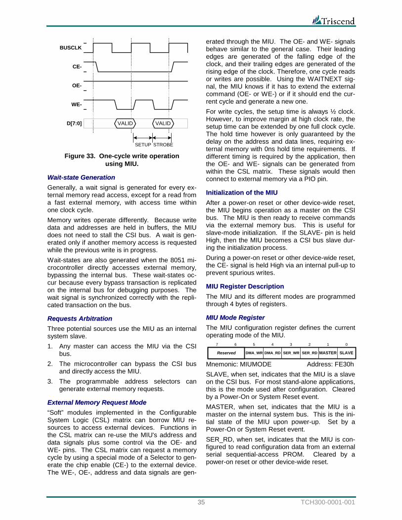
35 TCH300-0001-001
BUSCLK
CE-
OE-
WE-
D[7:0] VALID VALID
SETUP STROBE Figure 33. One-cycle write operation
using MIU.
WWaaiitt--ssttaattee GGeenneerraattiioonn Generally, a wait signal is generated for every ex-ternal memory read access, except for a read from a fast external memory, with access time within one clock cycle. Memory writes operate differently. Because write data and addresses are held in buffers, the MIU does not need to stall the CSI bus. A wait is gen-erated only if another memory access is requested while the previous write is in progress. Wait-states are also generated when the 8051 mi-crocontroller directly accesses external memory, bypassing the internal bus. These wait-states oc-cur because every bypass transaction is replicated on the internal bus for debugging purposes. The wait signal is synchronized correctly with the repli-cated transaction on the bus.
RReeqquueessttss AArrbbiittrraattiioonn Three potential sources use the MIU as an internal system slave. 1. Any master can access the MIU via the CSI
bus. 2. The microcontroller can bypass the CSI bus
and directly access the MIU. 3. The programmable address selectors can
generate external memory requests.
EExxtteerrnnaall MMeemmoorryy RReeqquueesstt MMooddee “Soft” modules implemented in the Configurable System Logic (CSL) matrix can borrow MIU re-sources to access external devices. Functions in the CSL matrix can re-use the MIU's address and data signals plus some control via the OE- and WE- pins. The CSL matrix can request a memory cycle by using a special mode of a Selector to gen-erate the chip enable (CE-) to the external device. The WE-, OE-, address and data signals are gen-
erated through the MIU. The OE- and WE- signals behave similar to the general case. Their leading edges are generated of the falling edge of the clock, and their trailing edges are generated of the rising edge of the clock. Therefore, one cycle reads or writes are possible. Using the WAITNEXT sig-nal, the MIU knows if it has to extend the external command (OE- or WE-) or if it should end the cur-rent cycle and generate a new one. For write cycles, the setup time is always ½ clock. However, to improve margin at high clock rate, the setup time can be extended by one full clock cycle. The hold time however is only guaranteed by the delay on the address and data lines, requiring ex-ternal memory with 0ns hold time requirements. If different timing is required by the application, then the OE- and WE- signals can be generated from within the CSL matrix. These signals would then connect to external memory via a PIO pin.
IInniittiiaalliizzaattiioonn ooff tthhee MMIIUU After a power-on reset or other device-wide reset, the MIU begins operation as a master on the CSI bus. The MIU is then ready to receive commands via the external memory bus. This is useful for slave-mode initialization. If the SLAVE- pin is held High, then the MIU becomes a CSI bus slave dur-ing the initialization process. During a power-on reset or other device-wide reset, the CE- signal is held High via an internal pull-up to prevent spurious writes.
MMIIUU RReeggiisstteerr DDeessccrriippttiioonn The MIU and its different modes are programmed through 4 bytes of registers.
MMIIUU MMooddee RReeggiisstteerr The MIU configuration register defines the current operating mode of the MIU.
SER_RD MASTER SLAVE
7 6 5 4 3 2 1 0
SER_WRDMA_RDDMA_WRReserved
Mnemonic: MIUMODE Address: FE30h SLAVE, when set, indicates that the MIU is a slave on the CSI bus. For most stand-alone applications, this is the mode used after configuration. Cleared by a Power-On or System Reset event. MASTER, when set, indicates that the MIU is a master on the internal system bus. This is the ini-tial state of the MIU upon power-up. Set by a Power-On or System Reset event. SER_RD, when set, indicates that the MIU is con-figured to read configuration data from an external serial sequential-access PROM. Cleared by a power-on reset or other device-wide reset.
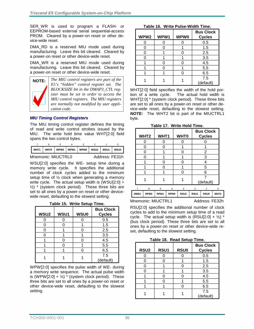
Triscend E5 Configurable System-on-Chip Platform
TCH300-0001-001 36
SER_WR is used to program a FLASH- or EEPROM-based external serial sequential-access PROM. Cleared by a power-on reset or other de-vice-wide reset. DMA_RD is a reserved MIU mode used during manufacturing. Leave this bit cleared. Cleared by a power-on reset or other device-wide reset. DMA_WR is a reserved MIU mode used during manufacturing. Leave this bit cleared. Cleared by a power-on reset or other device-wide reset.
NOTE:
The MIU control registers are part of the E5’s “hidden” control register set. The BLOCKSIZE bit in the DMAP3_CTL reg-ister must be set in order to access the MIU control registers. The MIU registers are normally not modified by user appli-cation code.
MMIIUU TTiimmiinngg CCoonnttrrooll RReeggiisstteerrss The MIU timing control register defines the timing of read and write control strobes issued by the MIU. The write hold time value WHT[2:0] field spans the two control bytes.
WSU2 WSU1 WSU0
7 6 5 4 3 2 1 0
WPW0WPW1WPW2WHT0WHT1
Mnemonic: MIUCTRL0 Address: FE31h WSU[2:0] specifies the WE- setup time during a memory write cycle. It specifies the additional number of clock cycles added to the minimum setup time of ½ clock when generating a memory write cycle. The actual setup width is (WSU[2:0] + ½) * (system clock period). These three bits are set to all ones by a power-on reset or other device-wide reset, defaulting to the slowest setting.
Table 15. Write Setup Time.
WSU2 WSU1 WSU0 Bus Clock
Cycles 0 0 0 0.5 0 0 1 1.5 0 1 0 2.5 0 1 1 3.5 1 0 0 4.5 1 0 1 5.5 1 1 0 6.5
1 1 1 7.5 (default)
WPW[2:0] specifies the pulse width of WE- during a memory write sequence. The actual pulse width is (WPW[2:0] + ½) * (system clock period). These three bits are set to all ones by a power-on reset or other device-wide reset, defaulting to the slowest setting.
Table 16. Write Pulse-Width Time.
WPW2 WPW1 WPW0 Bus Clock
Cycles 0 0 0 0.5 0 0 1 1.5 0 1 0 2.5 0 1 1 3.5 1 0 0 4.5 1 0 1 5.5 1 1 0 6.5
1 1 1 7.5 (default)
WHT[2:0] field specifies the width of the hold por-tion of a write cycle. The actual hold width is WHT[2:0] * (system clock period). These three bits are set to all ones by a power-on reset or other de-vice-wide reset, defaulting to the slowest setting. NOTE: The WHT2 bit is part of the MIUCTRL1 byte.
Table 17. Write Hold Time.
WHT2 WHT1 WHT0 Bus Clock
Cycles 0 0 0 0 0 0 1 1 0 1 0 2 0 1 1 3 1 0 0 4 1 0 1 5 1 1 0 6
1 1 1 7 (default)
RSU1 RSU0 WHT2
7 6 5 4 3 2 1 0
RSU2RPW0RPW1RPW2XMSU
Mnemonic: MIUCTRL1 Address: FE32h RSU[2:0] specifies the additional number of clock cycles to add to the minimum setup time of a read cycle. The actual setup width is (RSU[2:0] + ½) * (bus clock period). These three bits are set to all ones by a power-on reset or other device-wide re-set, defaulting to the slowest setting.
Table 18. Read Setup Time.
RSU2 RSU1 RSU0 Bus Clock
Cycles 0 0 0 0.5 0 0 1 1.5 0 1 0 2.5 0 1 1 3.5 1 0 0 4.5 1 0 1 5.5 1 1 0 6.5
1 1 1 7.5 (default)
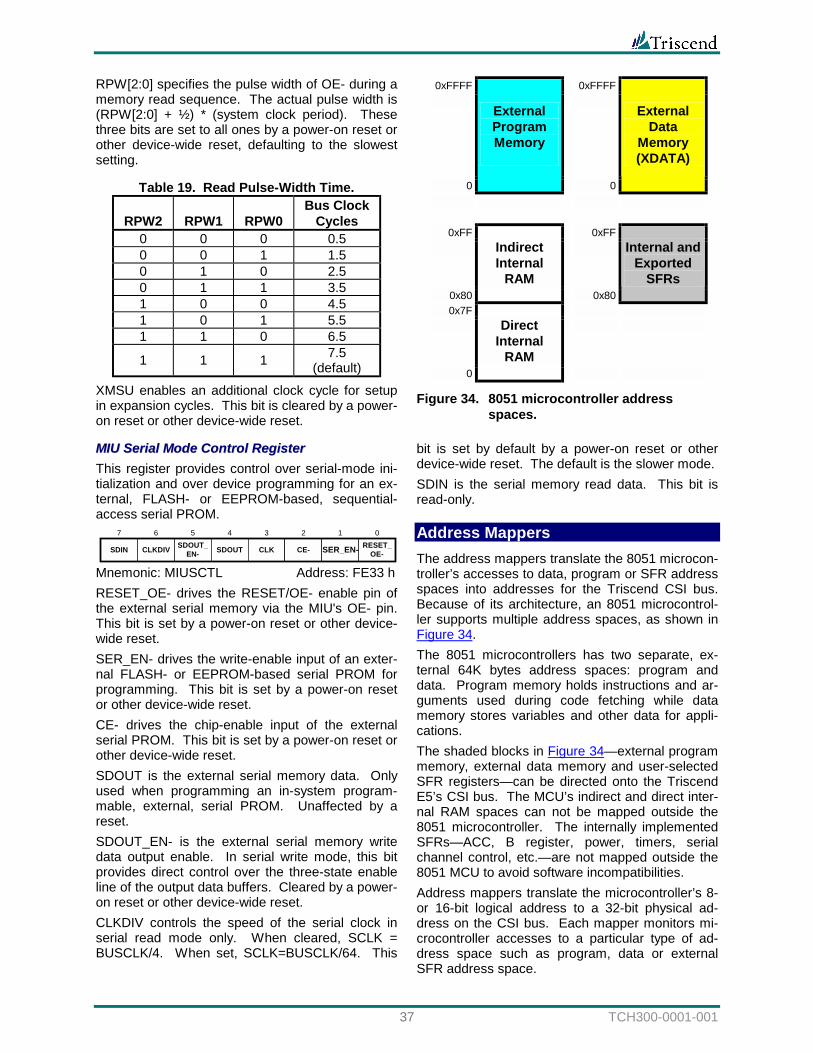
37 TCH300-0001-001
RPW[2:0] specifies the pulse width of OE- during a memory read sequence. The actual pulse width is (RPW[2:0] + ½) * (system clock period). These three bits are set to all ones by a power-on reset or other device-wide reset, defaulting to the slowest setting.
Table 19. Read Pulse-Width Time.
RPW2 RPW1 RPW0 Bus Clock
Cycles 0 0 0 0.5 0 0 1 1.5 0 1 0 2.5 0 1 1 3.5 1 0 0 4.5 1 0 1 5.5 1 1 0 6.5
1 1 1 7.5 (default)
XMSU enables an additional clock cycle for setup in expansion cycles. This bit is cleared by a power-on reset or other device-wide reset.
MMIIUU SSeerriiaall MMooddee CCoonnttrrooll RReeggiisstteerr This register provides control over serial-mode ini-tialization and over device programming for an ex-ternal, FLASH- or EEPROM-based, sequential-access serial PROM.
CE- SER_EN- RESET_OE-
7 6 5 4 3 2 1 0
CLKSDOUTSDOUT_EN-CLKDIVSDIN
Mnemonic: MIUSCTL Address: FE33 h RESET_OE- drives the RESET/OE- enable pin of the external serial memory via the MIU's OE- pin. This bit is set by a power-on reset or other device-wide reset. SER_EN- drives the write-enable input of an exter-nal FLASH- or EEPROM-based serial PROM for programming. This bit is set by a power-on reset or other device-wide reset. CE- drives the chip-enable input of the external serial PROM. This bit is set by a power-on reset or other device-wide reset. SDOUT is the external serial memory data. Only used when programming an in-system program-mable, external, serial PROM. Unaffected by a reset. SDOUT_EN- is the external serial memory write data output enable. In serial write mode, this bit provides direct control over the three-state enable line of the output data buffers. Cleared by a power-on reset or other device-wide reset. CLKDIV controls the speed of the serial clock in serial read mode only. When cleared, SCLK = BUSCLK/4. When set, SCLK=BUSCLK/64. This
bit is set by default by a power-on reset or other device-wide reset. The default is the slower mode. SDIN is the serial memory read data. This bit is read-only.
Address Mappers The address mappers translate the 8051 microcon-troller’s accesses to data, program or SFR address spaces into addresses for the Triscend CSI bus. Because of its architecture, an 8051 microcontrol-ler supports multiple address spaces, as shown in Figure 34. The 8051 microcontrollers has two separate, ex-ternal 64K bytes address spaces: program and data. Program memory holds instructions and ar-guments used during code fetching while data memory stores variables and other data for appli-cations. The shaded blocks in Figure 34—external program memory, external data memory and user-selected SFR registers—can be directed onto the Triscend E5’s CSI bus. The MCU’s indirect and direct inter-nal RAM spaces can not be mapped outside the 8051 microcontroller. The internally implemented SFRs—ACC, B register, power, timers, serial channel control, etc.—are not mapped outside the 8051 MCU to avoid software incompatibilities. Address mappers translate the microcontroller’s 8- or 16-bit logical address to a 32-bit physical ad-dress on the CSI bus. Each mapper monitors mi-crocontroller accesses to a particular type of ad-dress space such as program, data or external SFR address space.
0xFFFF 0xFFFF
0
External Program Memory
0
External Data
Memory (XDATA)
0xFF 0xFF
0x80
Indirect Internal
RAM 0x80
Internal and Exported
SFRs
0x7F
0
Direct Internal
RAM
Figure 34. 8051 microcontroller address spaces.
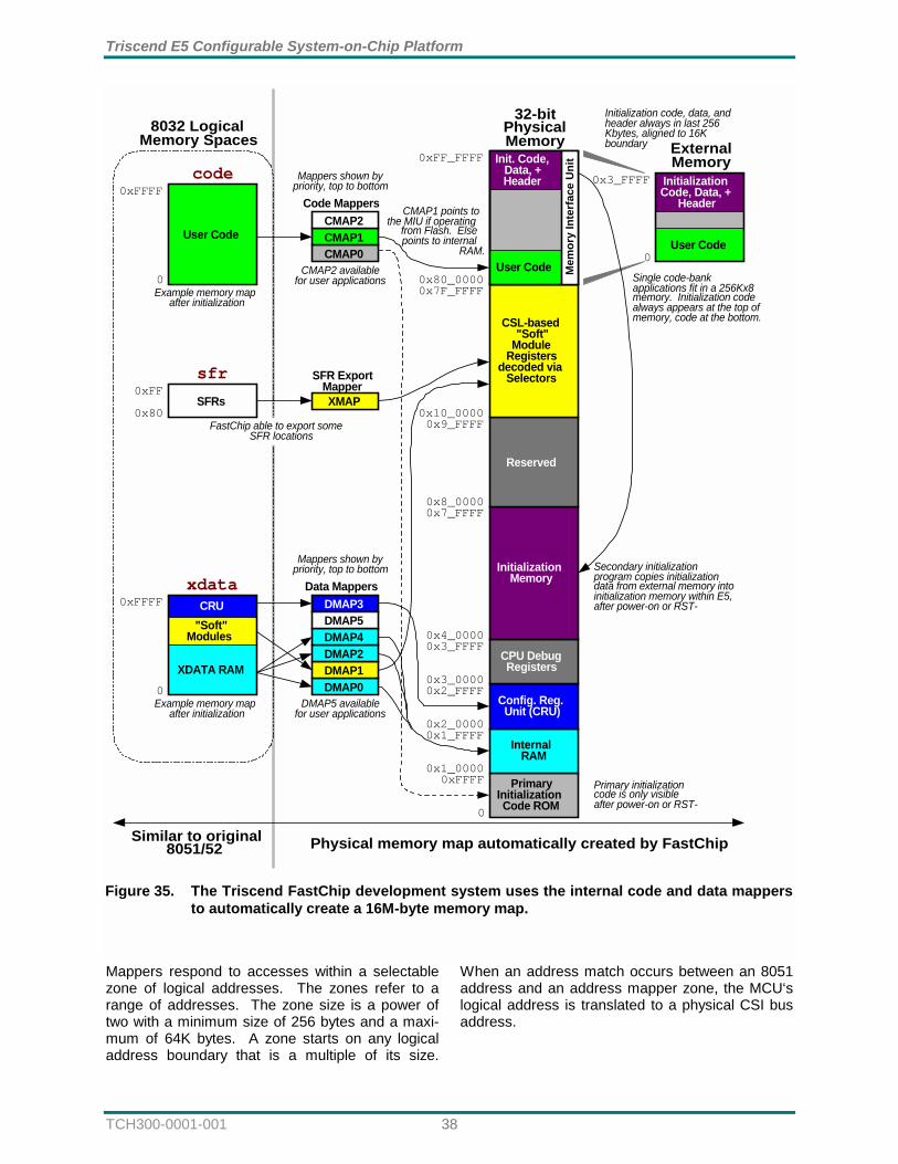
Triscend E5 Configurable System-on-Chip Platform
TCH300-0001-001 38
Mappers respond to accesses within a selectable zone of logical addresses. The zones refer to a range of addresses. The zone size is a power of two with a minimum size of 256 bytes and a maxi-mum of 64K bytes. A zone starts on any logical address boundary that is a multiple of its size.
When an address match occurs between an 8051 address and an address mapper zone, the MCU‘s logical address is translated to a physical CSI bus address.
PrimaryInitializationCode ROM
0
0xFFFF
InternalRAM
0x1_0000
0x1_FFFF
Config. Reg.Unit (CRU)
0x2_0000
0x2_FFFF
CPU DebugRegisters
0x3_0000
0x3_FFFF
InitializationMemory
0x4_0000
0x7_FFFF
Reserved
0x8_0000
0x9_FFFF
CSL-based"Soft"
ModuleRegisters
decoded viaSelectors
0x10_0000
0x7F_FFFF
0xFF_FFFF
0x80_0000
DMAP0DMAP1DMAP2
DMAP3
DMAP4DMAP5
CMAP0CMAP1CMAP2
0
0xFFFF CRU
XDATA RAM
"Soft"Modules
User Code
0
0xFFFF
Data Mappers
Code Mappers
0xFF
0x80
xdata
code
sfr
XMAP
SFR ExportMapper
User Code
Init. Code,Data, +Header
32-bitPhysicalMemory
8032 LogicalMemory Spaces
Primary initializationcode is only visibleafter power-on or RST-
DMAP5 availablefor user applications
CMAP2 availablefor user applications
Initialization code, data, andheader always in last 256Kbytes, aligned to 16Kboundary
FastChip able to export someSFR locations
0
0x3_FFFF InitializationCode, Data, +
Header
User Code
ExternalMemory
Secondary initializationprogram copies initializationdata from external memory intoinitialization memory within E5,after power-on or RST-
Example memory mapafter initialization
Example memory mapafter initialization
Mappers shown bypriority, top to bottom
Mappers shown bypriority, top to bottom
Single code-bankapplications fit in a 256Kx8memory. Initialization codealways appears at the top ofmemory, code at the bottom.
Mem
ory
Inte
rfac
e U
nit
SFRs
Similar to original8051/52 Physical memory map automatically created by FastChip
CMAP1 points tothe MIU if operating
from Flash. Elsepoints to internal
RAM.
Figure 35. The Triscend FastChip development system uses the internal code and data mappers
to automatically create a 16M-byte memory map.
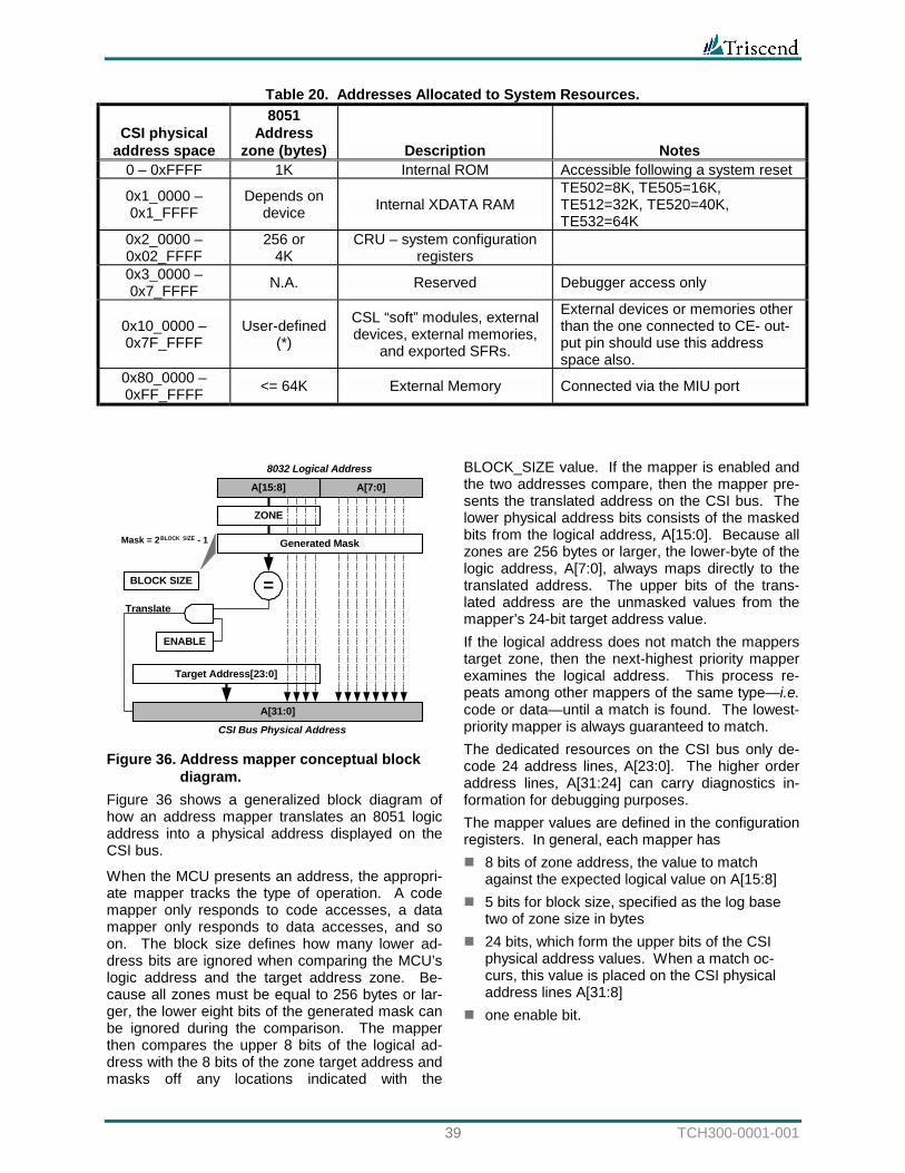
39 TCH300-0001-001
A[7:0]A[15:8]
8032 Logical Address
ZONE
BLOCK SIZE
ENABLE
=
A[31:0]
CSI Bus Physical Address
Mask = 2BLOCK_SIZE - 1
Target Address[23:0]
Translate
Generated Mask
Figure 36. Address mapper conceptual block
diagram. Figure 36 shows a generalized block diagram of how an address mapper translates an 8051 logic address into a physical address displayed on the CSI bus.
When the MCU presents an address, the appropri-ate mapper tracks the type of operation. A code mapper only responds to code accesses, a data mapper only responds to data accesses, and so on. The block size defines how many lower ad-dress bits are ignored when comparing the MCU’s logic address and the target address zone. Be-cause all zones must be equal to 256 bytes or lar-ger, the lower eight bits of the generated mask can be ignored during the comparison. The mapper then compares the upper 8 bits of the logical ad-dress with the 8 bits of the zone target address and masks off any locations indicated with the
BLOCK_SIZE value. If the mapper is enabled and the two addresses compare, then the mapper pre-sents the translated address on the CSI bus. The lower physical address bits consists of the masked bits from the logical address, A[15:0]. Because all zones are 256 bytes or larger, the lower-byte of the logic address, A[7:0], always maps directly to the translated address. The upper bits of the trans-lated address are the unmasked values from the mapper’s 24-bit target address value. If the logical address does not match the mappers target zone, then the next-highest priority mapper examines the logical address. This process re-peats among other mappers of the same type—i.e. code or data—until a match is found. The lowest-priority mapper is always guaranteed to match. The dedicated resources on the CSI bus only de-code 24 address lines, A[23:0]. The higher order address lines, A[31:24] can carry diagnostics in-formation for debugging purposes. The mapper values are defined in the configuration registers. In general, each mapper has ! 8 bits of zone address, the value to match
against the expected logical value on A[15:8] ! 5 bits for block size, specified as the log base
two of zone size in bytes ! 24 bits, which form the upper bits of the CSI
physical address values. When a match oc-curs, this value is placed on the CSI physical address lines A[31:8]
! one enable bit.
Table 20. Addresses Allocated to System Resources.
CSI physical address space
8051 Address
zone (bytes) Description Notes 0 – 0xFFFF 1K Internal ROM Accessible following a system reset
0x1_0000 – 0x1_FFFF
Depends on device Internal XDATA RAM
TE502=8K, TE505=16K, TE512=32K, TE520=40K, TE532=64K
0x2_0000 – 0x02_FFFF
256 or 4K
CRU – system configuration registers
0x3_0000 – 0x7_FFFF N.A. Reserved Debugger access only
0x10_0000 – 0x7F_FFFF
User-defined (*)
CSL “soft” modules, external devices, external memories,
and exported SFRs.
External devices or memories other than the one connected to CE- out-put pin should use this address space also.
0x80_0000 – 0xFF_FFFF <= 64K External Memory Connected via the MIU port
Triscend E5 Configurable System-on-Chip Platform
TCH300-0001-001 40
The block size results in a mask used during ad-dress matching. The block size is specified as the log base two of the desired address zone size, in bytes. The mask is a result of the following calcu-lation.
12 _ −= SizeBlockMask The lower 8 bits of the logical address are not part of the comparison. A block size must be in the range between 256 and 64K. Consequently, the block size value must be between 8 and 16, inclu-sive. Various system resources occupy non-contiguous address spaces in the 4G-byte address space available through the CSI bus. The Triscend Fast-Chip development system automatically creates a 16M-byte memory map as shown in Table 20 and Figure 35. The memory map is 16M bytes instead of the full 4G bytes because the upper eight bits of the physical address are assigned to the values shown in Table 23 to aid in debugging.
CCooddee mmaappppeerrss Code mappers perform address translations on code fetches. There are three code mappers, in-cluding a dedicated code mapper for the initializa-tion program stored in on-chip ROM plus two fully programmable code mappers. The code mappers are listed in Table 21.
Table 21. Code Mappers. Mapper Priority Enable
C2 1 Optional C1 2 Optional
C0 (ROM) 3 Always Enabled
CC00 –– RROOMM ccooddee mmaappppeerr The C0 mapper has the lowest priority. The inter-nal ROM is always accessible by the microcontrol-ler following a System Reset event. The ROM size is fixed at 1K byte, implemented with 64 copies that are available in the program space. The copies are repeated at every 1K byte boundary in code space. At the end of the initialization program, the other two code mappers, C1 and C2, can be pro-grammed to override the ROM code mapper. The C0 mapper has two programmable registers: CMAP0_TAR and CMAP0_ALT, both residing in the CRU. During a C0 address-matching event, the content of the CMAP0_TAR or CMAP0_ALT register is placed on the A[31:24] physical CSI bus address lines whenever an operand or an op-code fetch occurs, respectively. This feature is useful in debugging sessions to discriminate between op-code or operand fetches. C0 is always enabled.
CC00 OOppeerraanndd TTaarrggeett AAddddrreessss ((RROOMM mmaappppeerr))
A31 A30 A29 A28 A27 A26 A25 A24
7 6 5 4 3 2 1 0
Mnemonic: CMAP0_TAR Address: FF00h
CC00 OOpp--CCooddee TTaarrggeett AAddddrreessss ((RROOMM MMaappppeerr))
A31 A30 A29 A28 A27 A26 A25 A24
7 6 5 4 3 2 1 0
Mnemonic: CMAP0_ALT Address: FF01h
CC11,, CC22 –– FFuullllyy pprrooggrraammmmaabbllee ccooddee mmaappppeerrss Code mapper C2 has the highest priority in case of an address overlap with other code mappers. C1 and C2 can be individually enabled. Following a system reset, mappers C1 and C2 are disabled. Mapper C0 is always enabled. The Triscend ini-tialization program assigns application dependent values to these mappers. The user can modify these assignments by writing different values to the corresponding mapper registers.
CC11 TTaarrggeett AAddddrreessss ((LLooww BByyttee))
A15 A14 A13 A12 A11 A10 A9 A8
7 6 5 4 3 2 1 0
Mnemonic: CMAP1_TAR_0 Address: FF02h
CC11 TTaarrggeett AAddddrreessss ((MMiidd BByyttee))
A23 A22 A21 A20 A19 A18 A17 A16
7 6 5 4 3 2 1 0
Mnemonic: CMAP1_TAR_1 Address: FF03h
CC11 OOppeerraanndd TTaarrggeett AAddddrreessss
A31 A30 A29 A28 A27 A26 A25 A24
7 6 5 4 3 2 1 0
Mnemonic: CMAP1_TAR_2 Address: FF04h
CC11 OOpp--CCooddee TTaarrggeett AAddddrreessss
A31 A30 A29 A28 A27 A26 A25 A24
7 6 5 4 3 2 1 0
Mnemonic: CMAP1_ALT Address: FF07h
CC11 ZZoonnee SSoouurrccee AAddddrreessss
A15 A14 A13 A12 A11 A10 A9 A8
7 6 5 4 3 2 1 0
Mnemonic: CMAP1_SRC Address: FF05h
CC11 CCoonnttrrooll
- SIZE4 SIZE3 SIZE2 SIZE1 SIZE0- ENBL
7 6 5 4 3 2 1 0
Mnemonic: CMAP1_CTL Address: FF06h
41 TCH300-0001-001
CC22 TTaarrggeett AAddddrreessss ((LLooww BByyttee))
A15 A14 A13 A12 A11 A10 A9 A8
7 6 5 4 3 2 1 0
Mnemonic: CMAP2_TAR_0 Address: FF08h
CC22 TTaarrggeett AAddddrreessss ((MMiidd BByyttee))
A23 A22 A21 A20 A19 A18 A17 A16
7 6 5 4 3 2 1 0
Mnemonic: CMAP2_TAR_1 Address: FF09h
CC22 OOppeerraanndd TTaarrggeett AAddddrreessss
A31 A30 A29 A28 A27 A26 A25 A24
7 6 5 4 3 2 1 0
Mnemonic: CMAP2_TAR_2 Address: FF0Ah
CC22 OOpp--CCooddee TTaarrggeett AAddddrreessss
A31 A30 A29 A28 A27 A26 A25 A24
7 6 5 4 3 2 1 0
Mnemonic: CMAP2_ALT Address: FF0Dh
CC22 ZZoonnee SSoouurrccee AAddddrreessss
A15 A14 A13 A12 A11 A10 A9 A8
7 6 5 4 3 2 1 0
Mnemonic: CMAP2_SRC Address: FF0Bh
CC22 CCoonnttrrooll
- SIZE4 SIZE3 SIZE2 SIZE1 SIZE0- ENBL
7 6 5 4 3 2 1 0
Mnemonic: CMAP2_CTL Address: FF0Ch
DDaattaa mmaappppeerrss Data mappers perform address translations on data access instructions. There are six data map-pers as shown in Table 22. D0 maps accesses to the internal system SRAM. D1, D2, D4, and D5 are fully programmable and D3 maps the CRU configuration registers.
Table 22. Data Mappers. Mapper Priority Enable
D3 (CRU) 1 Always Enabled D5 2 Optional D4 3 Optional D2 4 Optional D1 5 Optional
D0 (RAM) 6 Always Enabled
DD00 –– RRAAMM ddaattaa mmaappppeerr The D0 has the lowest data mapping priority. The internal system RAM is always accessible by the microcontroller in data space following a System
Reset. The size and configuration of the internal system RAM is device dependent. For example, the RAM in the TE520 has a fixed size of 40K bytes. The bottom 32K bytes reside in data locations 0000h – 7FFFh. Four copies of the top 8K bytes appear at data locations 8000h, A000h, C000h and E000h, unless another data mapper is enabled and re-uses these locations. If enabled, data mappers D1 and D2 override RAM data space. The D3 mapper, used to access the configuration registers (CRU) always overrides the other mappers, as explained below. The D0 mapper has one programmable CRU register, DMAP0_TAR. The content of DMAP0_TAR is placed on the A[31:24] physical CSI bus address lines when a D0 matching event occurs. D0 is always enabled.
DD00 TTaarrggeett AAddddrreessss ((RRAAMM mmaappppeerr))
A31 A30 A29 A28 A27 A26 A25 A24
7 6 5 4 3 2 1 0
Mnemonic: DMAP0_TAR Address: FF0Eh
DD11,, DD22,, DD44,, DD55 –– FFuullllyy pprrooggrraammmmaabbllee ddaattaa mmaapp--ppeerrss Data mapper D5 has higher priority in case of an address overlap with D4, D2, D1 or D0. Mappers D5, D4, D2, and D1 can be individually enabled and are disabled after a System Reset event. The Triscend initialization program assigns application dependent values to these mappers. The user can modify these assignments by writing different val-ues to the corresponding mapper registers.
DD11 TTaarrggeett AAddddrreessss ((LLooww BByyttee))
A15 A14 A13 A12 A11 A10 A9 A8
7 6 5 4 3 2 1 0
Mnemonic: DMAP1_TAR_0 Address: FF0Fh
DD11 TTaarrggeett AAddddrreessss ((MMiidd BByyttee))
A23 A22 A21 A20 A19 A18 A17 A16
7 6 5 4 3 2 1 0
Mnemonic: DMAP1_TAR_1 Address: FF10h
DD11 TTaarrggeett AAddddrreessss ((HHiigghh BByyttee))
A31 A30 A29 A28 A27 A26 A25 A24
7 6 5 4 3 2 1 0
Mnemonic: DMAP1_TAR_2 Address: FF11h
DD11 ZZoonnee SSoouurrccee AAddddrreessss
A15 A14 A13 A12 A11 A10 A9 A8
7 6 5 4 3 2 1 0
Mnemonic: DMAP1_SRC Address: FF12h
Triscend E5 Configurable System-on-Chip Platform
TCH300-0001-001 42
DD11 CCoonnttrrooll
- SIZE4 SIZE3 SIZE2 SIZE1 SIZE0- ENBL
7 6 5 4 3 2 1 0
Mnemonic: DMAP1_CTL Address: FF13h
DD22 TTaarrggeett AAddddrreessss ((LLooww BByyttee))
A15 A14 A13 A12 A11 A10 A9 A8
7 6 5 4 3 2 1 0
Mnemonic: DMAP2_TAR_0 Address: FF14h
DD22 TTaarrggeett AAddddrreessss ((MMiidd BByyttee))
A23 A22 A21 A20 A19 A18 A17 A16
7 6 5 4 3 2 1 0
Mnemonic: DMAP2_TAR_1 Address: FF15h
DD22 TTaarrggeett AAddddrreessss ((HHiigghh BByyttee))
A31 A30 A29 A28 A27 A26 A25 A24
7 6 5 4 3 2 1 0
Mnemonic: DMAP2_TAR_2 Address: FF16h
DD22 ZZoonnee SSoouurrccee AAddddrreessss
A15 A14 A13 A12 A11 A10 A9 A8
7 6 5 4 3 2 1 0
Mnemonic: DMAP2_SRC Address: FF17h
DD22 CCoonnttrrooll
- SIZE4 SIZE3 SIZE2 SIZE1 SIZE0- ENBL
7 6 5 4 3 2 1 0
Mnemonic: DMAP2_CTL Address: FF18h
DD44 TTaarrggeett AAddddrreessss ((LLooww BByyttee))
A15 A14 A13 A12 A11 A10 A9 A8
7 6 5 4 3 2 1 0
Mnemonic: DMAP4_TAR_0 Address: FF80h
DD44 TTaarrggeett AAddddrreessss ((MMiidd BByyttee))
A23 A22 A21 A20 A19 A18 A17 A16
7 6 5 4 3 2 1 0
Mnemonic: DMAP4_TAR_1 Address: FF81h
DD44 TTaarrggeett AAddddrreessss ((HHiigghh BByyttee))
A31 A30 A29 A28 A27 A26 A25 A24
7 6 5 4 3 2 1 0
Mnemonic: DMAP4_TAR_2 Address: FF82h
DD44 ZZoonnee SSoouurrccee AAddddrreessss
A15 A14 A13 A12 A11 A10 A9 A8
7 6 5 4 3 2 1 0
Mnemonic: DMAP4_SRC Address: FF83h
DD44 CCoonnttrrooll
- SIZE4 SIZE3 SIZE2 SIZE1 SIZE0- ENBL
7 6 5 4 3 2 1 0
Mnemonic: DMAP4_CTL Address: FF84h
DD55 TTaarrggeett AAddddrreessss ((LLooww BByyttee))
A15 A14 A13 A12 A11 A10 A9 A8
7 6 5 4 3 2 1 0
Mnemonic: DMAP5_TAR_0 Address: FF85h
DD55 TTaarrggeett AAddddrreessss ((MMiidd BByyttee))
A23 A22 A21 A20 A19 A18 A17 A16
7 6 5 4 3 2 1 0
Mnemonic: DMAP5_TAR_1 Address: FF86h
DD55 TTaarrggeett AAddddrreessss ((HHiigghh BByyttee))
A31 A30 A29 A28 A27 A26 A25 A24
7 6 5 4 3 2 1 0
Mnemonic: DMAP5_TAR_2 Address: FF87h
DD55 ZZoonnee SSoouurrccee AAddddrreessss
A15 A14 A13 A12 A11 A10 A9 A8
7 6 5 4 3 2 1 0
Mnemonic: DMAP5_SRC Address: FF88h
DD55 CCoonnttrrooll
- SIZE4 SIZE3 SIZE2 SIZE1 SIZE0- ENBL
7 6 5 4 3 2 1 0
Mnemonic: DMAP5_CTL Address: FF89h
DD33 –– CCRRUU ddaattaa mmaappppeerr Data mapper D3 has the highest data mapping priority. The configuration registers (CRU) are al-ways accessible by the microcontroller. D3 has two selectable sizes of 4K and 256 bytes. Follow-ing a system reset, the D3 block size is set to 4K bytes and occupies the upper 4K bytes of the logi-cal data space, between addresses F000h and FFFFh, inclusive. At the end of the initialization program, the D3 data mapper zone is reduced to 256 bytes to conserve address space. D3 start address must be aligned to 4K address boundaries. All mapper registers are accessible through D3. The D3 mapper is always enabled.
DD33 TTaarrggeett AAddddrreessss
A31 A30 A29 A28 A27 A26 A25 A24
7 6 5 4 3 2 1 0
Mnemonic: DMAP3_TAR Address: FF19h
43 TCH300-0001-001
DD33 ZZoonnee SSoouurrccee AAddddrreessss
- - - - A15 A14 A13 A12
7 6 5 4 3 2 1 0
Mnemonic: DMAP3_SRC Address: FF1Ah
DD33 CCoonnttrrooll
- - - - -- -
7 6 5 4 3 2 1 0BLOCK
SIZE Mnemonic: DMAP3_CTL Address: FF1Bh When set, BLOCKSIZE defines the D3 mapper block size to 4K bytes. The BLOCKSIZE bit is set automatically at power-up. When cleared, the block size is reduced to 256 bytes.
SSFFRR eexxppoorrtt mmaappppeerr A Triscend configurable system-on-chip user can create custom microcontroller “soft” modules using the on-chip Configurable System Logic (CSL) ma-trix. These “soft” modules can be mapped into the 8051’s external data memory (XDATA) or into SFR space. If a CSL “soft” module is mapped into SFR space, then any control registers implemented in the CSL replace locations within the 8051’s SFR memory. The fully programmable SFR export mapper supplies a 32-bit address on the CSI bus whenever an external SFR access is detected. Fol-lowing a System Reset event, this mapper is dis-abled. The SFR export mapper has a special pro-grammable register called XMAP_ALT. The con-tent of XMAP_ALT or XMAP_TAR_2 is placed on the A31-A24 CSI bus address lines when a latch or a pin instruction occurs, respectively, during an external SFR access event. This feature can be useful in debugging sessions to discriminate be-tween various SFR instructions. Overall, there are 128 SFR-addressable locations in an 8051 microcontroller. Table 30 describes the SFRs within the MCU's scratchpad RAM. The Triscend FastChip development software prevents attempts to place CSL “soft” modules on internal SFR addresses already used by the MCU. The translated address, when accessing an ex-ported SFRs, consists of the XMAP_TAR_2 or XMAP_ALT register, the XMAP_TAR_1 register, and the XMAP_TAR_0 register appended to the A[7:0] address from the 8051 MCU. “Soft” modules with exported SFR registers can also be accessed via 8051 external-memory refer-ences, using the values loaded into the data map-pers. Placing “soft” module registers in the 8051’s SFR address space allows faster and simpler ac-cess using direct reference instructions. This method also enables the application code to use bit-manipulating instructions on these registers.
Application code usually never modifies the SFR export mapper registers. The register values are set during initialization.
SSFFRR EExxppoorrtt TTaarrggeett AAddddrreessss ((LLooww BByyttee))
A15 A14 A13 A12 A11 A10 A9 A8
7 6 5 4 3 2 1 0
Mnemonic: XMAP_TAR_0 Address: FE20h
SSFFRR EExxppoorrtt TTaarrggeett AAddddrreessss ((MMiidd BByyttee))
A23 A22 A21 A20 A19 A18 A17 A16
7 6 5 4 3 2 1 0
Mnemonic: XMAP_TAR_1 Address: FE21h
SSFFRR EExxppoorrtt TTaarrggeett AAddddrreessss ((LLaattcchh IInnssttrruuccttiioonn))
A31 A30 A29 A28 A27 A26 A25 A24
7 6 5 4 3 2 1 0
Mnemonic: XMAP_TAR_2 Address: FE22h
SSFFRR EExxppoorrtt TTaarrggeett AAddddrreessss ((PPiinn IInnssttrruuccttiioonn))
A31 A30 A29 A28 A27 A26 A25 A24
7 6 5 4 3 2 1 0
Mnemonic: XMAP_ALT Address: FE24h
DDeeffaauulltt VVaalluueess ffoorr HHiigghheerr--OOrrddeerr AAddddrreessss MMaapp--ppeerrss Table 23 shows the default assignment for higher address bits in each of the mappers. These values are loaded into the mapper registers during the initialization process. The Triscend FastChip development system uses these default values when assigning the 32-bit physical addresses for the CSL address selectors. These values and the mapper registers themselves allow CSL address selectors to selectively respond to different instruction types. For example, if a Flash memory device is con-nected to the MIU, some addresses can be ac-cessed as code or data segments. During normal operation, the Flash segment is typically used to store code. However, during a programming ses-sion, the Flash memory is regarded as a data segment. This differentiation between code and data using high order address lines distinguishes between code and data accesses to the same physical address. In another example, assume that an address selec-tor is used to enable off-chip ROM for external code storage. Code mapper C1 might point the ROM. The selector would need to respond to both operand and op-code fetches. Because CMAP1_TAR_2 = 00101000b and CMAP1_ALT = 000010000b, FastChip will program the upper byte of the selector's MASK register with 0010000, mak-
Triscend E5 Configurable System-on-Chip Platform
TCH300-0001-001 44
ing the selector respond to both operands and op-code fetches.
Table 23. Default Values for Higher-Order Ad-dress Mapper Registers.
Transaction Type Register Name
Default Value
A[31:24] C2 Operand Fetch CMAP2_TAR_2 30h
C2 Op-Code Fetch CMAP2_ALT 50h
C1 Operand Fetch CMAP1_TAR_2 28h
C1 Op-Code Fetch CMAP1_ALT 48h
C0 Operand Fetch (Init. ROM)
CMAP0_TAR_2 20h
C0 Op-Code Fetch (Init. ROM)
CMAP0_ALT 40h
D3 Data (CRU Regis-ters)
DMAP3_TAR_2 98h
D5 Data DMAP5_TAR_2 A8h D4 Data DMAP4_TAR_2 A0h D2 Data DMAP2_TAR_2 90h D1 Data DMAP1_TAR_2 88h D0 Data DMAP0_TAR_2 80h SFR Latch XMAP_ALT E0h SFR Pin XMAP_TAR_2 C0h
The mapper values are also used during debug-ging allowing the hardware breakpoint unit to dis-tinguish between operand and op-code fetches The distinction between SFR pin and SFR latch transactions is required only if the designer selects 8051-compatible PIO ports from Triscend "soft" module library. The 8051 microcontroller has in-structions that treat 8051 PIO ports differently than their respective SFR. In applications, there is no need for CSL address selectors to distinguish be-tween SFR latch and SFR pin instructions.
System Debugger
OOnn--CChhiipp DDeebbuuggggiinngg SSuuppppoorrtt A PC acting as an external tester or debugger can interface with the Triscend E5 configurable system-on-chip via its JTAG port, using a cable connected between the PC parallel port and the target board, as shown in Figure 37. The JTAG unit can access all addressable system resources by becoming the bus master on the in-ternal CSI bus. Serving as a bus master, the JTAG unit converts serial bitstreams into parallel registers
whose contents are placed on the address, data and command buses to emulate CSI bus transac-tions. A JTAG master also directly accesses inter-nal MCU registers and CSL configuration data with visibility to functions not accessible from application programs. Furthermore, the JTAG unit can hold the MCU in reset by asserting the J_RESET command or hold the entire system in reset using the FORCE_BRST and FORCE_NOBRST. The JTAG unit also inter-acts with the MCU using an interrupt handshake mechanism (J_INTR). For additional details, refer to the “Reset Conditions” section. The JTAG unit serves as a bus slave when inter-acting with the DMA controller. It first becomes master on the CSI bus, programs the DMA unit to transfer data to or from the JTAG unit, and then relinquishes the CSI bus to the DMA controller. After configuring the DMA, the JTAG unit interfaces with the DMA controller as a slave device using the DMA's request and acknowledge signals. There is considerably less overhead in this type of data transactions since the JTAG unit does not need to provide address or control information during DMA operations. Serving as a bus master, the JTAG unit is able to set breakpoint events within the breakpoint unit, which is also a slave connected on the CSI bus. The breakpoint unit supports two independent breakpoint conditions. The breakpoint unit moni-tors user-specified combinations of address, data, control or DMA signals as breakpoint events. The user can also count logic conditions occurring in-side the CSL as breakpoint events. A breakpoint specification can count up to 64K-1 incidents as the matching condition for a break event. Once a breakpoint condition occurs, then depend-ing on its current configuration, the MCU freezes at the end of the current instruction or receives a breakpoint interrupt and branches to execute de-bugger interrupt routines. Following a breakpoint freeze, CSL clocks or global signals can be blocked to aid system debugging. The Triscend FastChip software enables the user to specify which CSL clocks or global signals are affected following a breakpoint freeze. During a CPU freeze period, the JTAG unit can poll any addressable location residing inside or outside the CSoC and send all requested information to the host PC for further display and analysis. At the end of the debugging session, JTAG clears the breakpoint “freeze MCU” condition and the Ac-celerated 8051 microcontroller resumes code execution from where it left off. Alternatively, the JTAG unit can restart code execution from 0000h by issuing a J_RESET command to the MCU.
45 TCH300-0001-001
At any point in time, the JTAG unit can instruct the MCU to enter a single-step operation and send pertinent display information to the host PC. The JTAG port can also be used to initialize the CSoC or to update external memory devices con-nected to the MIU port. Using external Flash memory, the JTAG unit downloads a Flash-programming algorithm to the CSoC’s internal RAM. It then interacts with the internal MCU, al-lowing the processor to control the actual program / erase / verify algorithms while the JTAG port sup-plies new data for programming or new series of commands required by the MCU.
DDeebbuuggggiinngg SSuuppppoorrtt SSyysstteemm RReeqquuiirreemmeennttss Unlike debuggers for traditional 8051 designs, the E5 debugging environment does not require any additional system resources. The E5 environment does not use any additional code space nor does it consume a serial port. All debugging interaction is through the dedicated four-pin JTAG connection. The recommended debugging header, shown in Figure 38, connects to the Triscend JTAG Down-
Download/Debug cable. The header uses through-hole stake-pins on 0.1 inch centers.
GND2019
1817
+5 VDC Out
N.C. N.C.
1615 GNDN.C.
1413 N.C.N.C.
1211 GNDSystem Reset(open collector)
109TMS N.C.
87TCK N.C.
65N.C. +3.3 VDC Out(indicator only)
43
21
TDI
TDO
N.C.
N.C.(Top View)
Figure 38. Triscend E5 Download/Debug Cable
Header. Likewise, no special in-circuit emulator (ICE) is re-quired. The E5's on-chip breakpoint unit provides the capabilities available in most ICE systems.
Debug Host System
Free
ze
Inte
rrupt
Res
et
Inte
rrupt
JTAG
Inte
rface
Configurable System-on-Chip
UserCode
External Memory
InitializationData
CSI
BU
S(a
ddes
s,da
ta,c
ontr
ol,a
rbitr
atio
n)
MIU
Bus ResetDMA Req
DMA AckDMA
Controller
JTAGController
InternalSRAM
8032"Turbo"
MCU
BreakpointLogic
CSL LogicClockDisables
Figure 37. System debugging block diagram.
Triscend E5 Configurable System-on-Chip Platform
TCH300-0001-001 46
Configuration Register Unit (CRU) The Configuration Register Unit (CRU) contains the control registers for functions within the Tris-cend E5 configurable system-on-chip. For most applications, the CRU registers occupy the upper 256 bytes of external data space. Table 24 shows the functions controlled by the CRU registers. Unused locations have no function and are not RAM locations.
System Initialization Like most processors, the Triscend E5 requires initialization data to configure programmable op-tions available within the device before it becomes functional. The Triscend E5 offers four different system initialization options to best fit various target applications, as shown in Table 25. Both active and passive initialization methods are available.
In active initialization modes, the Triscend E5 pro-vides the control signals, directing data transfers and controlling external devices. In passive modes, an external controller directs data transfers.
Table 25. Initialization Modes. Initialization
Mode Method Data Source
Parallel Active Byte-wide parallel memory (FLASH)
Serial Active Sequential-access serial PROM
Secure Active Battery-backed in-ternal SRAM
JTAG Passive Downloaded by intel-ligent host through JTAG port
Slave Passive
Downloaded by other controller through bus inter-face.
Table 24. Configuration Register Unit (CRU). FF88h DMAP5_SRC DMAP5_CTL
FF80h DMAP4_TAR_0 [7:0]
DMAP4_TAR_1 [15:8]
DMAP4_TAR_2 [23:16] DMAP4_SRC DMAP4_CTL DMAP5_TAR_0
[7:0] DMAP5_TAR_1
[15:8] DMAP5_TAR_2
[23:16]
FF78h
FF70h
FF68h
FF60h PROTECT SECURITY PWDSEL PORCTRL
FF58h
FF50h
FF48h DMACRC_0 [7:0]
DMACRC_1 [15:8]
FF40h DMACADR1_1 [15:8]
DMACADR1_2 [23:16]
DMACADR1_3 [31:24]
DMACCNT1_0 [7:0]
DMACCNT1_1 [15:8]
DMACCNT1_2 [23:16]
DMAPREQ1_0 [7:0]
DMAPREQ1_1 [15:8]
FF38h DMASCNT1_0 [7:0]
DMASCNT1_1 [15:8]
DMASCNT1_2 [23:16]
DMACTRL1_0 [7:0]
DMACTRL1_1 [15:8] DMAEINT1 DMAINT1 DMACADR1_0
[7:0]
FF30h DMACCNT0_1 [15:8]
DMACCNT0_2 [23:16]
DMAPREQ0_0 [7:0]
DMAPREQ0_1 [15:8]
DMASADR1_0 [7:0]
DMASADR1_1 [15:8]
DMASADR1_2 [23:16]
DMASADR1_3 [31:24]
FF28h DMACTRL0_1 [15:8] DMAEINT0 DMAINT0 DMACADR0_0
[7:0] DMACADR0_1
[15:8] DMACADR0_2
[23:16] DMACADR0_3
[31:24] DMACCNT0_0
[7:0]
FF20h DMASADR0_0 [7:0]
DMASADR0_1 [15:8]
DMASADR0_2 [23:16]
DMASADR0_3 [31:24]
DMASCNT0_0 [7:0]
DMASCNT0_1 [15:8]
DMASCNT0_2 [23:16]
DMACTRL0_0 [7:0]
FF18h DMAP2_CTL DMAP3_TAR DMAP3_SRC DMAP3_CTL
FF10h DMAP1_TAR_1 [15:8]
DMAP1_TAR_2 [23:16] DMAP1_SRC DMAP1_CTL DMAP2_TAR_0
[7:0] DMAP2_TAR_1
[15:8] DMAP2_TAR_2
[23:16] DMAP2_SRC
FF08h CMAP2_TAR_0 [7:0]
CMAP2_TAR_1 [15:8]
CMAP2_TAR_2 [23:16] CMAP2_SRC CMAP2_CTL CMAP2_ALT DMAP0_TAR DMAP1_TAR_0
[7:0]
FF00h CMAP0_TAR CMAP0_ALT CMAP1_TAR_0 [7:0]
CMAP1_TAR_1 [15:8]
CMAP1_TAR_2 [23:16] CMAP1_SRC CMAP1_CTL CMAP1_ALT
Unused location, not RAM.
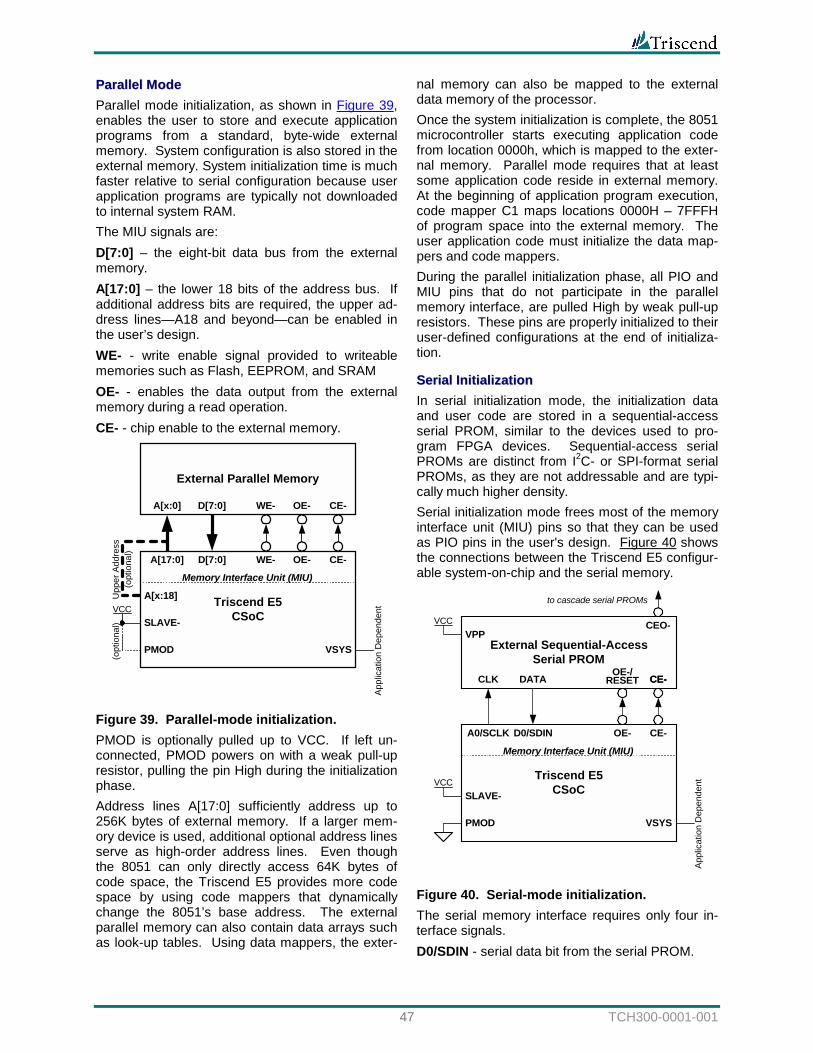
47 TCH300-0001-001
PPaarraalllleell MMooddee Parallel mode initialization, as shown in Figure 39, enables the user to store and execute application programs from a standard, byte-wide external memory. System configuration is also stored in the external memory. System initialization time is much faster relative to serial configuration because user application programs are typically not downloaded to internal system RAM. The MIU signals are: D[7:0] – the eight-bit data bus from the external memory. A[17:0] – the lower 18 bits of the address bus. If additional address bits are required, the upper ad-dress lines—A18 and beyond—can be enabled in the user’s design. WE- - write enable signal provided to writeable memories such as Flash, EEPROM, and SRAM OE- - enables the data output from the external memory during a read operation. CE- - chip enable to the external memory.
Triscend E5CSoC
A[17:0] D[7:0] WE- OE- CE-
SLAVE-
PMOD VSYS
Memory Interface Unit (MIU)
A[x:18]
CE-External Parallel Memory
OE-WE-D[7:0]A[x:0]
VCC
(opt
iona
l)U
pper
Add
ress
Appl
icat
ion
Dep
ende
nt
(opt
iona
l)
CE-
Figure 39. Parallel-mode initialization. PMOD is optionally pulled up to VCC. If left un-connected, PMOD powers on with a weak pull-up resistor, pulling the pin High during the initialization phase. Address lines A[17:0] sufficiently address up to 256K bytes of external memory. If a larger mem-ory device is used, additional optional address lines serve as high-order address lines. Even though the 8051 can only directly access 64K bytes of code space, the Triscend E5 provides more code space by using code mappers that dynamically change the 8051’s base address. The external parallel memory can also contain data arrays such as look-up tables. Using data mappers, the exter-
nal memory can also be mapped to the external data memory of the processor. Once the system initialization is complete, the 8051 microcontroller starts executing application code from location 0000h, which is mapped to the exter-nal memory. Parallel mode requires that at least some application code reside in external memory. At the beginning of application program execution, code mapper C1 maps locations 0000H – 7FFFH of program space into the external memory. The user application code must initialize the data map-pers and code mappers. During the parallel initialization phase, all PIO and MIU pins that do not participate in the parallel memory interface, are pulled High by weak pull-up resistors. These pins are properly initialized to their user-defined configurations at the end of initializa-tion.
SSeerriiaall IInniittiiaalliizzaattiioonn In serial initialization mode, the initialization data and user code are stored in a sequential-access serial PROM, similar to the devices used to pro-gram FPGA devices. Sequential-access serial PROMs are distinct from I2C- or SPI-format serial PROMs, as they are not addressable and are typi-cally much higher density. Serial initialization mode frees most of the memory interface unit (MIU) pins so that they can be used as PIO pins in the user's design. Figure 40 shows the connections between the Triscend E5 configur-able system-on-chip and the serial memory.
Triscend E5CSoC
A0/SCLK D0/SDIN OE- CE-
SLAVE-
PMOD VSYS
Memory Interface Unit (MIU)
CE-External Sequential-Access
Serial PROMOE-/
RESETDATACLK CE-
Appl
icat
ion
Dep
ende
nt
CE-
VPP
VCC
VCC CEO-
to cascade serial PROMs
Figure 40. Serial-mode initialization. The serial memory interface requires only four in-terface signals. D0/SDIN - serial data bit from the serial PROM.
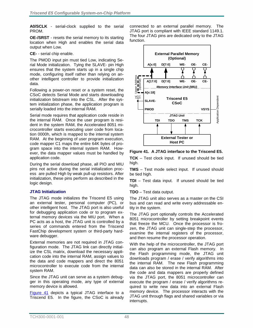
Triscend E5 Configurable System-on-Chip Platform
TCH300-0001-001 48
A0/SCLK - serial-clock supplied to the serial PROM. OE-/SRST - resets the serial memory to its starting location when High and enables the serial data output when Low. CE- - serial chip enable. The PMOD input pin must tied Low, indicating Se-rial Mode initialization. Tying the SLAVE- pin High ensures that the system starts up in a single chip mode, configuring itself rather than relying on an-other intelligent controller to provide initialization data. Following a power-on reset or a system reset, the CSoC detects Serial Mode and starts downloading initialization bitstream into the CSL. After the sys-tem initialization phase, the application program is serially loaded into the internal RAM. Serial mode requires that application code reside in the internal RAM. Once the user program is resi-dent in the system RAM, the Accelerated 8051 mi-crocontroller starts executing user code from loca-tion 0000h, which is mapped to the internal system RAM. At the beginning of user program execution, code mapper C1 maps the entire 64K bytes of pro-gram space into the internal system RAM. How-ever, the data mapper values must be handled by application code. During the serial download phase, all PIO and MIU pins not active during the serial initialization proc-ess are pulled High by weak pull-up resistors. After initialization, these pins perform as described in the logic design.
JJTTAAGG IInniittiiaalliizzaattiioonn The JTAG mode initializes the Triscend E5 using an external tester, personal computer (PC), or other intelligent host. The JTAG port is also useful for debugging application code or to program ex-ternal memory devices via the MIU port. When a PC acts as a host, the JTAG unit is controlled by a series of commands entered from the Triscend FastChip development system or third-party hard-ware debugger. External memories are not required in JTAG con-figuration mode. The JTAG link can directly initial-ize the CSL matrix, download the necessary appli-cation code into the internal RAM, assign values to the data and code mappers and direct the 8051 microcontroller to execute code from the internal system RAM. Since the JTAG unit can serve as a system debug-ger in this operating mode, any type of external memory device is allowed. Figure 41 depicts a typical JTAG interface to a Triscend E5. In the figure, the CSoC is already
connected to an external parallel memory. The JTAG port is compliant with IEEE standard 1149.1. The four JTAG pins are dedicated only to the JTAG function.
Triscend E5CSoC
A[17:0] D[7:0] WE- OE- CE-
SLAVE-
PMOD VSYS
TMSTDOTDI TCK
Memory Interface Unit (MIU)
JTAG Unit
A[x:18]
CE-
External Tester orHost PC
External Parallel Memory(Optional)
OE-WE-D[7:0]A[x:0]
VCC
(opt
iona
l)U
pper
Add
ress
Appl
icat
ion
Dep
ende
nt
CE-
Figure 41. A JTAG interface to the Triscend E5. TCK – Test clock input. If unused should be tied high. TMS – Test mode select input. If unused should be tied high. TDI – Test data input. If unused should be tied high. TDO – Test data output. The JTAG unit also serves as a master on the CSI bus and can read and write every addressable en-tity in the system. The JTAG port optionally controls the Accelerated 8051 microcontroller by setting breakpoint events that freeze the MCU. Once the processor is fro-zen, the JTAG unit can single-step the processor, examine the internal registers of the processor, and then resume the processor operation. With the help of the microcontroller, the JTAG port can also program an external Flash memory. In the Flash programming mode, the JTAG unit downloads program / erase / verify algorithms into the internal RAM. The new Flash programming data can also be stored in the internal RAM. After the code and data mappers are properly defined via the JTAG port, the 8051 microcontroller can execute the program / erase / verify algorithms re-quired to write new data into an external Flash memory device. The processor interacts with the JTAG unit through flags and shared variables or via interrupts.
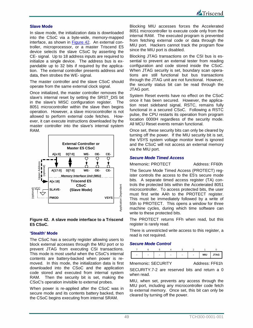
49 TCH300-0001-001
SSllaavvee MMooddee In slave mode, the initialization data is downloaded into the CSoC via a byte-wide, memory-mapped interface, as shown in Figure 42. An external con-troller, microprocessor, or a master Triscend E5 device selects the slave CSoC by asserting the CE- signal. Up to 18 address inputs are required to initialize a single device. The address bus is ex-pandable up to 32 bits if required by the applica-tion. The external controller presents address and data, then strobes the WE- signal. The master controller and the slave CSoC should operate from the same external clock signal. Once initialized, the master controller removes the slave's internal reset by setting the SRST_DIS bit in the slave's MISC configuration register. The 8051 microcontroller within the slave then begins operation. However, a slave microcontroller is not allowed to perform external code fetches. How-ever, it can execute instructions downloaded by the master controller into the slave's internal system RAM.
Triscend E5CSoC
(Slave Mode)
A[17:0] D[7:0] WE- OE- CE-
SLAVE-
PMOD VSYS
Memory Interface Unit (MIU)
A[x:18]
CE-External Controller or
Master E5 CSoCOE-WE-D[7:0]A[x:0]
(opt
iona
l)
Upp
er A
ddre
ss
Appl
icat
ion
Dep
ende
nt
(opt
iona
l)
CE-
VCC
Figure 42. A slave mode interface to a Triscend E5 CSoC.
''SStteeaalltthh'' MMooddee The CSoC has a security register allowing users to block external accesses through the MIU port or to prevent JTAG from executing CSI transactions. This mode is most useful when the CSoC's internal contents are battery-backed when power is re-moved. In this mode, the initialization data is first downloaded into the CSoC and the application code stored and executed from internal system RAM. Then the security bit is set, making the CSoC's operation invisible to external probes. When power is re-applied after the CSoC was in secure mode and its contents battery backed, then the CSoC begins executing from internal SRAM.
Blocking MIU accesses forces the Accelerated 8051 microcontroller to execute code only from the internal RAM. The executed program is prevented from fetching external code or data through the MIU port. Hackers cannot track the program flow since the MIU port is disabled. Blocking JTAG transactions on the CSI bus is es-sential to prevent an external tester from reading configuration and code stored inside the CSoC. When JTAG security is set, boundary scan opera-tions are still functional but bus transactions through the JTAG unit are not functional. However, the security status bit can be read through the JTAG port. System Reset events have no effect on the CSoC once it has been secured. However, the applica-tion reset sideband signal, RSTC, remains fully functional in a secured CSoC. Following a RSTC pulse, the CPU restarts its operation from program location 0000H regardless of the security mode. All MCU Reset events remain functional. Once set, these security bits can only be cleared by turning off the power. If the MIU security bit is set, the VSYS system voltage monitor level is ignored and the CSoC will not access an external memory via the MIU port.
SSeeccuurree MMooddee TTiimmeedd AAcccceessss Mnemonic: PROTECT Address: FF60h The Secure Mode Timed Access (PROTECT) reg-ister controls the access to the E5's secure mode bits. A separate timed access register (TA) con-trols the protected bits within the Accelerated 8051 microcontroller. To access protected bits, the user must first write AAh to the PROTECT register. This must be immediately followed by a write of 55h to PROTECT. This opens a window for three machine cycles, during which time software can write to these protected bits. The PROTECT returns FFh when read, but this register is rarely read. There is unrestricted write access to this register, a read is not required.
SSeeccuurree MMooddee CCoonnttrrooll
- - - - - - MIU JTAG
7 6 5 4 3 2 1 0
Mnemonic: SECURITY Address: FF61h SECURITY.7-2 are reserved bits and return a 0 when read. MIU, when set, prevents any access through the MIU port, including any microcontroller code fetch to external memory. Once set, this bit can only be cleared by turning off the power.
Triscend E5 Configurable System-on-Chip Platform
TCH300-0001-001 50
JTAG, when set, prevents any access through the JTAG port. Once set, this bit can only be cleared by turning off the power. A write cycle to the security register must be pre-ceded by two data-specific, back-to-back write op-erations to the Protect register. A write operation to the Protect register with a data pattern of AAh must be followed by a write operation to the Protect register with a data value of 55h. Any write cycle directed at a different CSI location or containing a different data pattern would reset the write protect mechanism. After both write cycles are detected in the right order and match the above-specified data patterns, a write to the Security register is enabled for a single write cycle. The JTAG secure and MIU secure bits are active high. Once set they can only be cleared by turning off the power. The 8051 microcontroller can al-ways read the security register to determine or ver-ify that the part is secured.
SSiizzee ooff IInniittiiaalliizzaattiioonn DDaattaa The size of the initialization data file depends on which E5 family device is used in the application and the initialization method used.
IInniittiiaalliizzaattiioonn DDaattaa SSiizzee Each device has a predefined number of rows and columns of initialization information as shown in Table 26. The total data size is the product of the number of rows and columns.
Table 26. Initialization Data Size. Device Columns Rows Total Bytes TE502 102 120 12,240 TE505 102 208 21,216 TE512 144 296 42,624 TE520 186 384 71,424 TE532 228 472 107,616
PPaarraalllleell MMooddee SSeeccoonnddaarryy IInniittiiaalliizzaattiioonn PPrrooggrraamm The secondary initialization program loads an E5 device with the initialization data. The initialization program consists of 8051 instructions. The total size of the secondary initialization data image for parallel mode operation consists of ! 967 bytes of 8051 instruction code to load the
initialization data into the E5 device ! 19 bytes of initialization data header and footer
information ! the initialization data file from Table 26 ! 94 bytes of 8051 instruction code to set up the
data and code mappers after loading the initiali-zation data.
Because the secondary initialization program al-ways resides within the top 256 Kbytes of external
memory, aligned to a 16K boundary, the absolute size of the data is larger than actual data file. Table 27 shows the total size of the secondary ini-tialization data, including the initialization program, and the memory requirements once the initializa-tion data is aligned to a 16 Kbyte boundary.
Table 27. Parallel Mode Memory Requirements.
Device Secondary Init.
Data Size Total Memory Requirements
TE502 13,320 16K TE505 22,296 32K TE512 43,704 48K TE520 72,504 80K TE532 108,696 112K
TTiimmee ttoo IInniittiiaalliizzee aann EE55 CCSSooCC DDeevviiccee
PPaarraalllleell IInniittiiaalliizzaattiioonn The time to initialize an E5 device depends on the device used and the frequency of the bus clock. After power-on or after RST- is asserted, the E5 device begins initialization clocked from the internal ring oscillator. The frequency of the internal ring oscillator is minimum of 5 MHz and a maximum of 20 MHz. During the initialization process, the bus clock source can be switched over to an external clock source or to the crystal oscillator amplifier, both of which operate up to 25 or 40 MHz, depend-ing on the speed grade. Table 28 shows the initialization time using various frequency bus clock inputs. If bus clock is clocked from the crystal oscillator amplifier, allow an addi-tional 5 ms for crystal settling time. If using the special 32 kHz mode for the crystal oscillator amplifier, allow 200 ms settling time.
Table 28. Estimated Parallel Initialization Times at Various Bus Clock Frequencies.
Bus Clock Frequency Device 1 MHz 5 MHz 25 MHz 40 MHz TE502 94 ms 19 ms 4.5 ms 3.1 ms TE505 112 ms 23 ms 5.2 ms 3.6 ms TE512 181 ms 37 ms 8.0 ms 5.3 ms TE520 265 ms 54 ms 11.4 ms 7.4 ms TE532 364 ms 73 ms 15.3 ms 9.9 ms
VVSSYYSS CCoonnttrrooll A power-on reset or other device-wide reset causes the Triscend E5 to start the initialization process as shown in Table 39. The VSYS input pin directs the system initialization state machine how to behave should the initialization process fail to find valid external initialization data. If the VSYS pin is held High through the initializa-tion phase and no valid configuration pattern is found, then the CSoC automatically powers down
51 TCH300-0001-001
to conserve power. Another Power-On Reset or System Reset event is required to restart the ini-tialization process. However, if VSYS is sampled Low during the ini-tialization process, the CSoC device attempts to re-start the initialization process following a failed ini-tialization attempt. The initialization mode, whether serial or parallel, is determined from the PMOD pin. If VSYS is tied to GND, the CSoC will attempt re-configuring itself indefinitely until it finds valid ini-tialization data. This option might be useful when the system operates in noisy environments.
NOTE:
VSYS must connect to a valid logic level. Do not leave VSYS unconnected.
In applications using a system supervisory chip, a “VCC good” output from the supervisory device can connect to VSYS, ensuring that initialization only takes place when VCC is within the proper operat-ing voltage range. If the MIU security bit is set, the VSYS level is ig-nored and the CSoC will not access an external memory via the MIU port.
Clocking and Global Signal Distribution The Triscend E5 configurable system-on-chip pro-vides powerful, flexible clocking resources. A sys-tem-wide bus clock (BCLK) provides clocking to most of the E5 device. In addition, six global buff-ers supply additional clocks or high-fanout signals for the CSL matrix.
SSyysstteemm cclloocckk sseelleecctt ((BBCCLLKK)) The system clock, called BCLK, supplies the clock to the Accelerated 8051 microcontroller, its dedi-cated resources, and to the CSI bus. Additionally, BCLK is distributed globally to the CSL matrix and to the PIO pins. There are three potential user-defined sources for BCLK. 1. An internal ring oscillator operates at frequen-
cies ranging between 5 MHz to 20 MHz, as shown in Figure 43. The ring oscillator fre-quency is temperature, voltage, and process dependent. The internal ring oscillator can be shut off during power-down mode by setting the OSC bit (PWDSEL.3).
XTALINLeaveunconnected
BCLK
OSCPWDSEL.3
Internal RingOscillator
(~5 - 20 MHz)
Figure 43. Internal ring oscillator.
2. A crystal oscillator amplifier—connected inter-nally between the BCLK/XTAL and XTALOUT pins—supports 32 kHz operation and frequen-cies from 2 MHz up to 40 MHz, as shown in Figure 44. A crystal and the external circuitry listed in Table 29 generate the desired fre-quency. The crystal oscillator amplifier also supports ceramic resonators. The crystal os-cillator output can be turned off during power-down mode by setting the XTAL bit (PWDSEL.4). Frequencies above 24 MHz re-quire the crystal to operate in the third over-tone. The crystal operates in its fundamental mode at lower frequencies. The internal feed-back resistor should also be enabled using the FastChip development system.
Table 29. Crystal Oscillator External Component Values.
Crystal Frequency
Range
Suggested External
Resistor (R1)
External Capacitor
(C1 and C2) 32 kHz 10 MΩ 10 pF
2 MHz—24 MHz (fundamental) 1 MΩ 10 pF
24 MHz—40 MHz (third overtone) 4.7 kΩ 10 pF
C1
C2
XTAL
XTALIN
BCLK/XTALBCLK
XTALPWDSEL.4
R1
Figure 44. Crystal oscillator input.
3. A user-provided logic signal supplies the oper-ating clock frequency when applied to the XTAL input pin. The XTALOUT pin should be left unconnected, as shown in Figure 45.
Triscend E5 Configurable System-on-Chip Platform
TCH300-0001-001 52
BCLK/XTAL
XTALIN
Clock input signal
Leaveunconnected
Figure 45. Clock input from external system.
The device always powers up using the internal oscillator, which serves as the system clock during the system initialization phase. The system switches over to the user selected clock source sometime before the MCU starts executing the ap-plication program. In most applications, the user-defined clock source is the crystal-oscillator clock (XTAL). Two copies of the selected clock source propagate in the CSoC. The BCLK signal is shared by all dedicated resources connected to the CSI bus, including the MCU, DMA, mappers, programmable system decoders, etc. The CSL_BCLK propagates into the CSL matrix and optionally connects to pro-grammable CSL “soft” modules and PIO pins. Usually, the system clock source is selected at de-sign time and unchanged by software. However, application code may need to modify the selection if the crystal oscillator is turned off during power-down mode. See "Power-On Reset Control" for more information.
SSyysstteemm CClloocckk SSeelleecctt RReeggiisstteerr
- - - - - - SCPU_ENA
BCLKSEL
7 6 5 4 3 2 1 0
Mnemonic: MISC Address: FE81h MISC.7-2 are reserved locations that return 0 when read. SCPU_ENA, when set, releases the CPU reset caused when the SLAVE- input is Low. Used only in Slave mode applications. BCLKSEL, when set, selects the crystal oscillator or an incoming, external clock source on the XTAL input pin. When cleared, then the internal ring os-cillator provides the system clock. When the SLAVE- pin is Low, the BCLKSEL bit is forced to 1.
SSiixx GGlloobbaall BBuuffffeerrss In addition to system clock, there are six global signals available from within the CSL matrix. The six signals, GBUF[5:0], are buffered and provide a high-speed, low skew distribution path for addi-tional clocks or high-fanout signals.
CClloocckk aanndd GGlloobbaall SSiiggnnaall SSttooppppiinngg The system clock and the outputs from the six global buffers can be optionally stopped during power-down and debugging sessions.
BBuuss CClloocckk SSttooppppiinngg aanndd SSiinnggllee--SStteeppppiinngg When stopped by a breakpoint event, the MCU completes the current instructions before stopping the bus clock, BCLK.
GGlloobbaall BBuuffffeerr SSttoopp VVaalluuee The six global buffers have a selectable value when stopped. During design, each global buffer is optionally configured to one of the following func-tions. 1. Actively drive the global buffer, regardless of a
stop event. 2. Latch the last state of the global buffer and
drive the resulting value. 3. Force the buffer output Low.
Accelerated 8051 Microcontroller Architecture The Accelerated 8051 microcontroller, embedded in the Triscend E5, is based on the standard 8051 device. The E5 is built around an 8-bit ALU that uses internal registers for temporary storage and to control peripheral devices. It executes the stan-dard 8051 instruction set. A brief description of the internal blocks follows.
AALLUU The ALU is the heart of the 8051 microcontroller and performs arithmetic and logical functions. It also makes decisions for jump instructions, and calculates jump addresses. The ALU is not directly user accessible, but the instruction decoder reads the op-code, decodes it, and sequences the data through the ALU and its associated registers to generate the required result. The ALU primarily uses the ACC, which is a Special Function Register (SFR) on the chip. Another SFR, the B Register, is also used in Multiply and Divide instructions. The ALU generates several status signals that are stored in the Program Status Word register (PSW).
AAccccuummuullaattoorr The Accumulator (ACC) is the primary register used in arithmetic, logical and data transfer opera-tions in the configurable system-on-chip. Since the Accumulator is directly accessible by the microcon-troller, most of the high-speed instructions use the ACC as one argument.
BB RReeggiisstteerr This 8-bit register is used as the second argument in the MUL and DIV instructions. For all other in-structions, it is simply a general-purpose register.
53 TCH300-0001-001
PPrrooggrraamm SSttaattuuss WWoorrdd This is an 8-bit SFR that stores the status bits of the ALU. It holds the Carry flag, the Auxiliary Carry flag, General purpose flags, the Register Bank Se-lect, the Overflow flag, and the Parity flag.
DDaattaa PPooiinntteerrss MOVX instructions use the Data Pointers to trans-fer data to and from Data locations. These point-ers hold the address of the memory location to which data is transferred. Because data can be moved to and from external memory, the configur-able system-on-chip provides two separate Data Pointers. The user can switch between either of the two Data Pointers with minimum software overhead, greatly increasing system throughput.
SSccrraattcchh--ppaadd RRAAMM The 8051 has a 256-byte scratchpad RAM within the microcontroller. Scratchpad RAM is useful for temporary storage during program execution. Cer-tain sections of this RAM are bit addressable, and directly addressed by the 8051’s powerful Boolean instructions.
SSttaacckk PPooiinntteerr The 8051 has an 8-bit Stack Pointer that points to the top of the Stack. The stack resides in the scratchpad RAM in the processor. Consequently, the size of the stack is limited by the size of this RAM.
TTiimmeerrss//CCoouunntteerrss The configurable system-on-chip has three 16-bit Timer/Counters. Each timer inhabits two SFR lo-cations that software can read or write. Other SFR locations, associated with the timers, control their mode and operation.
SSeerriiaall PPoorrtt The 8051 microcontroller provides one serial I/O port that operates in both synchronous and asyn-chronous modes. The serial port inhabits several SFR locations.
MMeemmoorryy OOrrggaanniizzaattiioonn The 8051, a classic Harvard architecture device, separates the memory into two sections, the pro-
gram memory and the data memory. The program memory stores the instruction op-codes, while the data memory stores data values or accesses memory-mapped devices.
PPrrooggrraamm MMeemmoorryy The 8051 supports up to 64K bytes of program memory. This memory space is either stored ex-ternally—typically in FLASH memory—or internally using the E5’s internal system RAM. All instruc-tions are fetched for execution from this memory area. The MOVC instruction also accesses this memory region.
DDaattaa MMeemmoorryy The 8051 supports up to 64K bytes of data mem-ory. This memory region is accessed by the MOVX instructions. In addition, the 8051 microcontroller has 256 bytes of scratchpad RAM, plus can access an additional 8K bytes to 64K bytes of internal sys-tem RAM—the memory size depends on the spe-cific device. Scratchpad RAM locations are ac-cessed either by direct addressing or by indirect addressing. The microcontroller’s Special Function Registers (SFRs) can only be accessed by direct addressing.
RReeggiisstteerr MMaapp The 8051 has separate program and data memory areas. The on-chip 256-byte scratchpad RAM is in addition to the on-chip system RAM and any exter-nal memory. There are also several SFRs ac-cessed by software. The SFRs are only accessible through direct addressing, while the on-chip scratchpad RAM is accessible through either direct or indirect addressing. Since the scratchpad RAM, shown in Figure 46, is only 256 bytes deep, it can be used only when data contents are small. Larger amounts of data should be stored either in the internal system RAM or in external data memory. However, on-chip system RAM has faster access times than external RAM. There are several other special-purpose areas within the scratchpad RAM. These are described as follows.
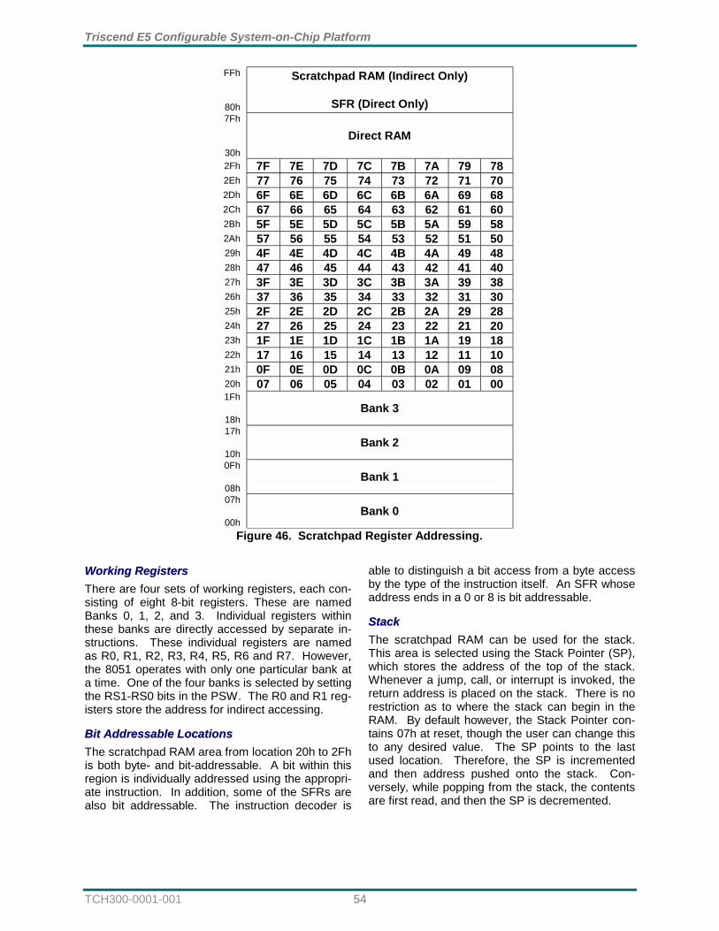
Triscend E5 Configurable System-on-Chip Platform
TCH300-0001-001 54
WWoorrkkiinngg RReeggiisstteerrss There are four sets of working registers, each con-sisting of eight 8-bit registers. These are named Banks 0, 1, 2, and 3. Individual registers within these banks are directly accessed by separate in-structions. These individual registers are named as R0, R1, R2, R3, R4, R5, R6 and R7. However, the 8051 operates with only one particular bank at a time. One of the four banks is selected by setting the RS1-RS0 bits in the PSW. The R0 and R1 reg-isters store the address for indirect accessing.
BBiitt AAddddrreessssaabbllee LLooccaattiioonnss The scratchpad RAM area from location 20h to 2Fh is both byte- and bit-addressable. A bit within this region is individually addressed using the appropri-ate instruction. In addition, some of the SFRs are also bit addressable. The instruction decoder is
able to distinguish a bit access from a byte access by the type of the instruction itself. An SFR whose address ends in a 0 or 8 is bit addressable.
SSttaacckk The scratchpad RAM can be used for the stack. This area is selected using the Stack Pointer (SP), which stores the address of the top of the stack. Whenever a jump, call, or interrupt is invoked, the return address is placed on the stack. There is no restriction as to where the stack can begin in the RAM. By default however, the Stack Pointer con-tains 07h at reset, though the user can change this to any desired value. The SP points to the last used location. Therefore, the SP is incremented and then address pushed onto the stack. Con-versely, while popping from the stack, the contents are first read, and then the SP is decremented.
FFh
80h
Scratchpad RAM (Indirect Only)
SFR (Direct Only) 7Fh
30h
Direct RAM
2Fh 7F 7E 7D 7C 7B 7A 79 78 2Eh 77 76 75 74 73 72 71 70 2Dh 6F 6E 6D 6C 6B 6A 69 68 2Ch 67 66 65 64 63 62 61 60 2Bh 5F 5E 5D 5C 5B 5A 59 58 2Ah 57 56 55 54 53 52 51 50 29h 4F 4E 4D 4C 4B 4A 49 48 28h 47 46 45 44 43 42 41 40 27h 3F 3E 3D 3C 3B 3A 39 38 26h 37 36 35 34 33 32 31 30 25h 2F 2E 2D 2C 2B 2A 29 28 24h 27 26 25 24 23 22 21 20 23h 1F 1E 1D 1C 1B 1A 19 18 22h 17 16 15 14 13 12 11 10 21h 0F 0E 0D 0C 0B 0A 09 08 20h 07 06 05 04 03 02 01 00 1Fh
18h
Bank 3
17h
10h Bank 2
0Fh
08h Bank 1
07h
00h Bank 0
Figure 46. Scratchpad Register Addressing.
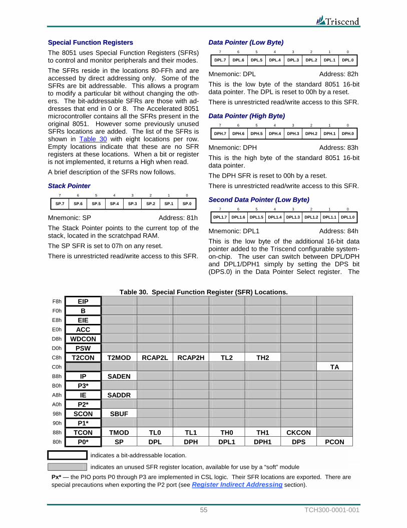
55 TCH300-0001-001
SSppeecciiaall FFuunnccttiioonn RReeggiisstteerrss The 8051 uses Special Function Registers (SFRs) to control and monitor peripherals and their modes. The SFRs reside in the locations 80-FFh and are accessed by direct addressing only. Some of the SFRs are bit addressable. This allows a program to modify a particular bit without changing the oth-ers. The bit-addressable SFRs are those with ad-dresses that end in 0 or 8. The Accelerated 8051 microcontroller contains all the SFRs present in the original 8051. However some previously unused SFRs locations are added. The list of the SFRs is shown in Table 30 with eight locations per row. Empty locations indicate that these are no SFR registers at these locations. When a bit or register is not implemented, it returns a High when read. A brief description of the SFRs now follows.
SSttaacckk PPooiinntteerr
SP.7 SP.6 SP.5 SP.4 SP.3 SP.2 SP.1 SP.0
7 6 5 4 3 2 1 0
Mnemonic: SP Address: 81h The Stack Pointer points to the current top of the stack, located in the scratchpad RAM. The SP SFR is set to 07h on any reset. There is unrestricted read/write access to this SFR.
DDaattaa PPooiinntteerr ((LLooww BByyttee))
DPL.7 DPL.6 DPL.5 DPL.4 DPL.3 DPL.2 DPL.1 DPL.0
7 6 5 4 3 2 1 0
Mnemonic: DPL Address: 82h This is the low byte of the standard 8051 16-bit data pointer. The DPL is reset to 00h by a reset. There is unrestricted read/write access to this SFR.
DDaattaa PPooiinntteerr ((HHiigghh BByyttee))
DPH.7 DPH.6 DPH.5 DPH.4 DPH.3 DPH.2 DPH.1 DPH.0
7 6 5 4 3 2 1 0
Mnemonic: DPH Address: 83h This is the high byte of the standard 8051 16-bit data pointer. The DPH SFR is reset to 00h by a reset. There is unrestricted read/write access to this SFR.
SSeeccoonndd DDaattaa PPooiinntteerr ((LLooww BByyttee))
DPL1.7 DPL1.6 DPL1.5 DPL1.4 DPL1.3 DPL1.2 DPL1.1 DPL1.0
7 6 5 4 3 2 1 0
Mnemonic: DPL1 Address: 84h This is the low byte of the additional 16-bit data pointer added to the Triscend configurable system-on-chip. The user can switch between DPL/DPH and DPL1/DPH1 simply by setting the DPS bit (DPS.0) in the Data Pointer Select register. The
Table 30. Special Function Register (SFR) Locations. F8h EIP F0h B E8h EIE E0h ACC D8h WDCON D0h PSW C8h T2CON T2MOD RCAP2L RCAP2H TL2 TH2 C0h TA B8h IP SADEN B0h P3* A8h IE SADDR A0h P2* 98h SCON SBUF 90h P1* 88h TCON TMOD TL0 TL1 TH0 TH1 CKCON 80h P0* SP DPL DPH DPL1 DPH1 DPS PCON
indicates a bit-addressable location.
indicates an unused SFR register location, available for use by a “soft” module Px* — the PIO ports P0 through P3 are implemented in CSL logic. Their SFR locations are exported. There are special precautions when exporting the P2 port (see Register Indirect Addressing section).
Triscend E5 Configurable System-on-Chip Platform
TCH300-0001-001 56
instructions using DPTR will then access DPL1 and DPH1 in place of DPL and DPH. If DPL1/DPH1 are not used, then they can be used an conventional register locations. The DPL1 SFR is reset to 00h by a reset. There is unrestricted read/write access to this SFR.
SSeeccoonndd DDaattaa PPooiinntteerr ((HHiigghh BByyttee))
DPH1.7 DPH1.6 DPH1.5 DPH1.4 DPH1.3 DPH1.2 DPH1.1 DPH1.0
7 6 5 4 3 2 1 0
Mnemonic: DPH1 Address: 85h This is the high byte of the additional 16-bit data pointer added to the Triscend configurable system-on-chip. The user can switch between DPL/DPH and DPL1/DPH1 simply by setting DPS = 1. The instructions using DPTR will then access DPL1 and DPH1 in place of DPL and DPH. If DPL1/DPH1 are not used as a data pointer, then they can be used as conventional register locations. The DPH1 SFR is reset to 00h by a reset. There is unrestricted read/write access to this SFR.
DDaattaa PPooiinntteerr SSeelleecctt
RESERVED (Reads = 0) DPS.0
7 6 5 4 3 2 1 0
Mnemonic: DPS Address: 86h DPS.0 selects either the DPL/DPH pair or the DPL1/DPH1 pair as the active Data Pointer. When set to 1, DPL1/DPH1 is selected, else DPL/DPH is selected. DPS.1-7 are reserved but will read 0. The DPS SFR is reset to 00h by a reset and se-lects the standard DPTR by default. There is unrestricted read/write access to this SFR.
PPoowweerr CCoonnttrrooll
SMOD SMOD0 - - GF1 GF0 PD IDL
7 6 5 4 3 2 1 0
Mnemonic: PCON Address: 87h SMOD, when set, doubles the serial baud rate when the serial port is in Modes 1, 2, and 3. SMOD0 is the Framing Error Detection Enable. When SMOD0 is set to 1, then SCON.7 indicates a Frame Error and acts as the FE flag. When SMOD0 is 0, then SCON.7 behaves as a standard 8051 function. GF1-0 are two general-purpose user flag bits. Setting the PD bit causes the configurable system-on-chip to go into the power-down mode. In this mode, all the clocks are stopped and program exe-cution is halted. While in power-down mode, addi-
tional low-power options are enabled, controlled by the PWDSEL. See "Clocking and Global Signal Distribution" for more details. Setting the IDL bit causes the Accelerated 8051 microcontroller to go into the IDLE mode. In this mode, the clock to the microcontroller is stopped, halting program execution. However, the clock to the serial, timer and interrupt blocks is not stopped, and these blocks continue operating unhindered. The PCON SFR is reset to 00110000b by a reset. There is unrestricted read/write access to this SFR.
TTiimmeerr CCoonnttrrooll
TF1 TR1 TF0 TR0 IE1 IT1 IE0 IT0
7 6 5 4 3 2 1 0
Mnemonic: TCON Address: 88h TF1 is the Timer 1 overflow flag. This bit is set when Timer 1 overflows and is cleared automati-cally when the program executes a Timer 1 inter-rupt service routine. Software can also set or clear this bit. TR1 is the Timer 1 run control bit. This bit is set or cleared by software to turn Timer 1 on or off. TF0 is the Timer 0 overflow flag. This bit is set when Timer 0 overflows and is cleared automati-cally when the program executes a timer 0 interrupt service routine. Software can also set or clear this bit. TR0 is the Timer 0 run control bit. This bit is set or cleared by software to turn Timer 0 on or off. IE1 is the Interrupt 1 edge-detect flag. It is set by hardware when an edge/level is detected on the INTR1 sideband signal. This bit is cleared by hard-ware when the service routine is vectored to only if the interrupt was edge triggered. Otherwise, it tracks the value that appears on the INIT1 side-band signal.
NOTE:
The polarity of the external interrupt sig-nals, INTR0 and INTR1, are opposite that of the original 8051. In the original 8051, these signals are falling-edge trig-gered or active-Low level. In the E5 fam-ily, these signals are rising-edge trig-gered or active-High level.
IT1 is the Interrupt 1 type control bit. It is set by software to specify a rising-edge trigger, cleared to specify an active-High level-triggered external in-put. IE0 is the Interrupt 0 edge-detect flag. It is set by hardware when an edge/level is detected on the INTR0 sideband signal. This bit is cleared by hard-ware when the service routine is vectored to only if the interrupt was edge triggered. Otherwise, it
57 TCH300-0001-001
tracks the value that appears the INIT0 sideband signal. IT0 is the Interrupt 0 type control bit. It is set by software to specify a rising-edge trigger, cleared to specify an active-High level-triggered external in-put. The TCON SFR is reset to 00h by a reset. There is unrestricted read/write access to this SFR.
TTiimmeerr MMooddee CCoonnttrrooll
GATE C/T M1 M0 GATE C/T M1 M0
7 6 5 4 3 2 1 0
Timer 1 Timer 0 Mnemonic: TMOD Address: 89h GATE is the Gating control bit. When this bit is set, Timer/counter x is enabled only while INTRx pin is high and TRx control bit is set. When GATE is cleared, the TRx bit (TR0 for Timer 0, TR1 for Timer 1) enables the timer when set. C/T is the Timer or Counter Select bit. When cleared, the timer increments on internal clocks. When set, the timer counts high-to-low edges of the Tx (T0 for Timer 0, T1 for Timer 1) sideband signal.
Table 31. Timer 0 and Timer 1 Mode Select Bits.
M1 M0 Mode 0 0 Mode 0: 8-bits with 5-bit pre-scaler. 0 1 Mode 1: 16-bits, no pre-scaler.
1 0 Mode 2: 8-bits with auto-reload from THx
1 1
Mode 3: (Timer 0) TL0 is an 8-bit timer/counter controlled by the Timer 0 control bits. TH0 is a 8-bit timer only controlled by Timer 1 control bits. (Timer 1) Timer/counter is stopped.
M1 and M0 are the Mode Select bits. They control the operation of the Timer/Counter as defined in Table 31. The TMOD is reset to 00h by a reset. There is unrestricted read/write access to this SFR.
TTiimmeerr 00 LLSSBB Mnemonic: TL0 Address: 8Ah TL0.7-0 is the least-significant byte of Timer 0. The TL0 SFR is set to 00h on any reset. There is unrestricted read/write access to this SFR.
TTiimmeerr 11 LLSSBB Mnemonic: TL1 Address: 8Bh TL1.7-0 is the least-significant byte of Timer 1. The TL1 SFR is set to 00h on any reset.
There is unrestricted read/write access to this SFR.
TTiimmeerr 00 MMSSBB Mnemonic: TH0 Address: 8Ch TH0.7-0 is the most-significant byte of Timer 0. The TH0 SFR is set to 00h on any reset. There is unrestricted read/write access to this SFR.
TTiimmeerr 11 MMSSBB Mnemonic: TH1 Address: 8Dh TH1.7-0 is the most-significant byte of Timer 1. The TH1 SFR is set to 00h on any reset. There is unrestricted read/write access to this SFR. TH1 potentially also controls the baud for the 8051' serial port, when the serial port operates in variable baud rate mode, i.e., Mode 1 or Mode 3. The equation for controlling the baud rate is shown below, where SMOD is PCON.7, F is the bus clock frequency, and Baud is the desired rate.
••−=Baud384F2256ROUNDTH1 busclock
SMOD
The resulting value may be a non-integer. Round the value up or down, whichever most closely matches the desired baud rate. In some instances, selecting a different bus clock frequency will result in a value closer to the desired baud rate.
CClloocckk CCoonnttrrooll
WD1 WD0 T2M T1M T0M - - -
7 6 5 4 3 2 1 0
Mnemonic: CKCON Address: 8Eh WD1-0 are the Watchdog timer mode select bits. These bits determine the time-out period for the watchdog timer. For all four of the time-out op-tions, the reset time-out is 512 clocks after the in-terrupt time-out period, as shown in Table 32.
Table 32. Watchdog Timer Modes.
WD1 WD0 Interrupt time-out
Reset time-out
0 0 217 217 + 512 0 1 220 220 + 512 1 0 223 223 + 512 1 1 226 226 + 512
T2M is the Timer 2 clock select bit. When T2M is set to 1, Timer 2 uses a divide-by-4 clock. When set to 0, Timer 2 uses an 8051-compatible divide-by-12 clock. T1M is the Timer 1 clock select bit. When T1M is set to 1, Timer 1 uses a divide-by-4 clock. When
Triscend E5 Configurable System-on-Chip Platform
TCH300-0001-001 58
set to 0, Timer 1 uses an 8051-compatible divide-by-12 clock. T0M is the Timer 0 clock select bit. When T0M is set to 1, Timer 0 uses a divide-by-4 clock. When set to 0, Timer 0 uses an 8051-compatible divide-by-12 clock. CKCON.2-0 are reserved. The CKCON SFR is set to 00h on any reset. There is unrestricted read/write access to this SFR.
SSeerriiaall PPoorrtt CCoonnttrrooll
SM0/FE SM1 SM2 REN TB8 RB8 TI RI
7 6 5 4 3 2 1 0
Mnemonic: SCON Address: 98h SM0/FE performs as either Serial port, Mode 0 bit or as the Framing Error Flag. The SMOD0 bit in PCON SFR determines whether this bit acts as SM0 or as FE. The operation of SM0 is described in Table 33. When used as FE, this bit is set to indicate an inva-lid stop bit. Software must clear the FE condition. SM1 is the Serial port Mode bit 1. SM2 is the Serial port Mode bit 2, which controls multiple MCU communication. Setting this bit en-ables the multiprocessor communication feature in Mode 2 and 3. In Mode 2 or 3, if SM2 is set, then RI is not activated if the received 9th data bit (RB8) is 0. In Mode 1, if SM2 = 1, then RI is only acti-vated if a valid stop bit is received. In Mode 0, the SM2 bit controls the serial port clock. If cleared, then the serial port runs at 1/12 the system clock frequency, providing compatibility with the standard 8051. When set, the serial clock is 1/4 the system clock frequency, resulting in faster synchronous serial communication.
Table 33. Serial Mode Control Values.
SM0 SM1 Mode Descrip-
tion Length Baud rate
0 0 0 Synch. 8 BUSCLK ÷4/÷12
0 1 1 Asynch. 10 variable
1 0 2 Asynch. 11 BUSCLK ÷64/÷32
1 1 3 Asynch. 11 variable
REN is the Receiver enable bit. Setting this bit to 1 enables serial reception, else reception is disabled. TB8 is the 9th bit to be transmitted in Modes 2 and 3. This bit is set and cleared by software as de-sired. RB8 is the received 9th data bit in Modes 2 and 3. In mode 1, if SM2 = 0, RB8 is the received stop bit value. In Mode 0, it has no function.
TI is the Transmit interrupt flag. This flag is set by hardware at the end of the 8th bit time in mode 0, or at the beginning of the stop bit in all other modes during serial transmission. This bit must be cleared by software. RI is the Receive interrupt flag. This flag is set by hardware at the end of the 8th bit time in mode 0, or halfway through the stop bits time in the other modes during serial reception. However, the re-striction on SM2 applies on this bit. This bit can be cleared only by software The SCON SFR is set to 00h by a reset. There is unrestricted read/write access to this SFR.
SSeerriiaall DDaattaa BBuuffffeerr Mnemonic: SBUF Address: 99h SBUF.7-0 is the serial data, read from or written to this location. It actually consists of two separate 8-bit registers. One is the receive register and the other is the transmit buffer. Any read access gathers data from the receive data buffer, while write transfers are to the transmit data buffer. The SBUF SFR is set to 00h by a reset. There is unrestricted read/write access to this SFR.
IInntteerrrruupptt EEnnaabbllee
EA - ET2 ES ET1 EX1 ET0 EX0
7 6 5 4 3 2 1 0
Mnemonic: IE Address: A8h EA, when set, is the global enable bit and enables all interrupts. When cleared, this bit disables all interrupts, except for HPINT. IE.6 is an un-implemented bit. It returns a High when read. ET2, when set, enables the Timer 2 interrupt. ES, when set, enables the Serial interrupt. ET1, when set, enables the Timer 1 interrupt. EX1, when set, enables External interrupt 1. ET0, when set, enables the Timer 0 interrupt. EX0, when set, enables External interrupt 0. The IE SFR is set to 01000000b by a reset. There is unrestricted read/write access to this SFR.
SSllaavvee AAddddrreessss Mnemonic: SADDR Address: A9h SADDR is used only during multiple MCU opera-tions involving the serial port. SADDR is loaded with the given or broadcast ad-dress for the serial port if the E5 is used as a slave processor during multiprocessor communications.
59 TCH300-0001-001
The SADDR SFR is set to 00h by a reset. There is unrestricted read/write access to this SFR.
IInntteerrrruupptt PPrriioorriittyy
- - PT2 PS PT1 PX1 PT0 PX0
7 6 5 4 3 2 1 0
Mnemonic: IP Address: B8h The IP.7-6 bits are un-implemented and return a High when read. PT2, when set, defines the Timer 2 interrupt as a higher priority interrupt. PS, when set, defines the Serial port interrupt as a higher priority interrupt. PT1, when set, defines the Timer 1 interrupt as a higher-priority interrupt. PX1, when set, defines the External Interrupt 1 as a higher-priority interrupt. PT0, when set, defines the Timer 0 interrupt as a higher-priority interrupt. PX0, when set, defines External Interrupt 0 as a higher-priority interrupt. The IP SFR is set to 11000000b by a reset. There is unrestricted read/write access to this SFR.
SSllaavvee AAddddrreessss MMaasskk EEnnaabbllee Mnemonic: SADEN Address: B9h The SADEN register enables the Automatic Ad-dress Recognition feature of the Serial port. When a bit in the SADEN is set to 1, the same bit location in SADDR is compared with the incoming serial port data. When SADEN is 0, then the bit becomes a don’t-care in the comparison. When all the bits of SADEN are 0, an interrupt occurs for any incom-ing address. The SADEN SFR is set to 00h by a reset. There is unrestricted read/write access to this SFR.
TTiimmeedd AAcccceessss Mnemonic: TA Address: C7h The Timed Access (TA) register controls the ac-cess to protected Watchdog controller bits in the 8051 microcontroller. A separate timed access register (PROTECT) supports the secure initializa-tion mode. To access protected bits, application software must first write AAh to the TA SFR. This must be immediately followed by a write of 55h to TA. This opens a window for three machine cy-cles, during which time software can write to these protected bits. The TA returns FFh when read. There is unrestricted write access to this SFR, a read is not required.
Example: MOV TA, 0AAH ; Write ‘AA’ followed by ‘55’ to open
; window MOV TA, 055H ; Window now open for three machine
; cycles SETB RWT ; Reset watchdog timer
TTiimmeerr 22 CCoonnttrrooll
TF2 EXF2 RCLK TCLK EXEN2 TR2 C/T2 CP/RL2
7 6 5 4 3 2 1 0
Mnemonic: T2CON Address: C8h TF2 is the Timer 2 overflow flag. This bit is set when Timer 2 overflows. It is also set when the count equals the capture register value while in down count mode. It can be set only if RCLK and TCLK are both 0. It is only cleared by software. Software can also set or clear this bit. EXF2 is the Timer 2 External Flag. A falling-edge transition on the T2EX sideband signal or a Timer 2 underflow/overflow condition sets this flag based on the CP/RL2, EXEN2 and DCEN bits. If set by a falling-edge transition, this flag must be cleared by software. Setting this bit in software or a detected falling-edge transition on T2EX pin forces a timer interrupt, if enabled. RCLK is the Receive clock flag. This bit deter-mines the serial port timebase when receiving data in serial modes 1 or 3. If this bit is 0, then Timer 1 overflow is used for baud rate generation, else Timer 2 overflow is used. Setting this bit forces Timer 2 into baud-rate generator mode. TCLK is the Transmit clock flag. This bit deter-mines the serial port timebase when transmitting data in serial modes 1 and 3. If it is set to 0, the Timer 1 overflow is used to generate the baud rate clock, else Timer 2 overflow is used. Setting this bit forces Timer 2 into baud-rate generator mode. EXEN2 is the Timer 2 External Enable bit. This bit enables the capture/reload function on the T2EX sideband signal if Timer 2 is not generating baud clocks for the serial port. If this bit is 0, then the T2EX sideband signal is ignored, else a falling-edge transition detected on the T2EX sideband signal results in capture or reload. TR2 is the Timer 2 Run Control bit. This bit en-ables/disables the operation of Timer 2. Halting Timer 2 by clearing this bit preserves the current count value in TH2, TL2. C/T2 is the Counter/Timer select bit. This bit de-termines whether Timer 2 functions as a timer (counting clock cycles) or as a counter. Independ-ent of this bit, the timer runs at 2 clocks per tick when used in baud rate generator mode. If it is set to 0, then Timer 2 operates as a timer at a speed
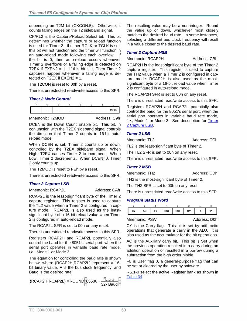
Triscend E5 Configurable System-on-Chip Platform
TCH300-0001-001 60
depending on T2M bit (CKCON.5). Otherwise, it counts falling edges on the T2 sideband signal. CP/RL2 is the Capture/Reload Select bit. This bit determines whether the capture or reload function is used for Timer 2. If either RCLK or TCLK is set, this bit will not function and the timer will function in an auto-reload mode following each overflow. If the bit is 0, then auto-reload occurs whenever Timer 2 overflows or a falling edge is detected on T2EX if EXEN2 = 1. If this bit is 1, Then Timer 2 captures happen whenever a falling edge is de-tected on T2EX if EXEN2 = 1. The T2CON is reset to 00h by a reset. There is unrestricted read/write access to this SFR.
TTiimmeerr 22 MMooddee CCoonnttrrooll
- - - - - - - DCEN
7 6 5 4 3 2 1 0
Mnemonic: T2MOD Address: C9h DCEN is the Down Count Enable bit. This bit, in conjunction with the T2EX sideband signal controls the direction that Timer 2 counts in 16-bit auto-reload mode. When DCEN is set, Timer 2 counts up or down, controlled by the T2EX sideband signal. When High, T2EX causes Timer 2 to increment. When Low, Timer 2 decrements. When DCEN=0, Timer 2 only counts up. The T2MOD is reset to FEh by a reset. There is unrestricted read/write access to this SFR.
TTiimmeerr 22 CCaappttuurree LLSSBB Mnemonic: RCAP2L Address: CAh RCAP2L is the least-significant byte of the Timer 2 capture register. This register is used to capture the TL2 value when a Timer 2 is configured in cap-ture mode. RCAP2L is also used as the least-significant byte of a 16-bit reload value when Timer 2 is configured in auto-reload mode. The RCAP2L SFR is set to 00h on any reset. There is unrestricted read/write access to this SFR. Registers RCAP2H and RCAP2L potentially also control the baud for the 8051's serial port, when the serial port operates in variable baud rate mode, i.e., Mode 1 or Mode 3. The equation for controlling the baud rate is shown below, where RCAP2H,RCAP2L represent a 16-bit binary value, F is the bus clock frequency, and Baud is the desired rate.
•−=
Baud32F65536ROUNDRCAP2LRCAP2H, busclock
The resulting value may be a non-integer. Round the value up or down, whichever most closely matches the desired baud rate. In some instances, selecting a different bus clock frequency will result in a value closer to the desired baud rate.
TTiimmeerr 22 CCaappttuurree MMSSBB Mnemonic: RCAP2H Address: CBh RCAP2H is the least-significant byte of the Timer 2 capture register. This register is used to capture the TH2 value when a Timer 2 is configured in cap-ture mode. RCAP2H is also used as the most-significant byte of a 16-bit reload value when Timer 2 is configured in auto-reload mode. The RCAP2H SFR is set to 00h on any reset. There is unrestricted read/write access to this SFR. Registers RCAP2H and RCAP2L potentially also control the baud for the 8051's serial port, when the serial port operates in variable baud rate mode, i.e., Mode 1 or Mode 3. See description for Timer 2 Capture LSB.
TTiimmeerr 22 LLSSBB Mnemonic: TL2 Address: CCh TL2 is the least-significant byte of Timer 2. The TL2 SFR is set to 00h on any reset. There is unrestricted read/write access to this SFR.
TTiimmeerr 22 MMSSBB Mnemonic: TH2 Address: CDh TH2 is the most-significant byte of Timer 2. The TH2 SFR is set to 00h on any reset. There is unrestricted read/write access to this SFR.
PPrrooggrraamm SSttaattuuss WWoorrdd
CY AC F0 RS1 RS0 OV F1 P
7 6 5 4 3 2 1 0
Mnemonic: PSW Address: D0h CY is the Carry flag. This bit is set by arithmetic operations that generate a carry in the ALU. It is also used as the accumulator for the bit operations. AC is the Auxiliary carry bit. This bit is Set when the previous operation resulted in a carry during an addition operation or resulted in a borrow during a subtraction from the high order nibble. F0 is User flag 0, a general-purpose flag that can be set or cleared by the user by software. RS.1-0 select the active Register bank as shown in Table 34.
61 TCH300-0001-001
Table 34. Register Bank Select.
RS1 RS0 Register
bank Address 0 0 0 00-07h 0 1 1 08-0Fh 1 0 2 10-17h 1 1 3 18-1Fh
OV is the Overflow flag. Set by arithmetic opera-tions. Indicates that two most significant accumu-lator bits are different. Used primarily with signed or twos-compliment data to indicate that the arith-metic operation overflowed the accuracy of the ac-cumulator. F1 is User Flag 1, a general-purpose flag that can be set or cleared by the user by software P is the Parity flag. This bit is set or cleared by hardware to indicate odd/even number of 1’s in the accumulator. The PSW SFR is set to 00h by a reset. There is unrestricted read/write access to this SFR.
WWaattcchhddoogg CCoonnttrrooll
- POR EHPI HPI WDIF WTRF EWT RWT
7 6 5 4 3 2 1 0
Write protected by Timed-Access (TA) register Mnemonic: WDCON Address: D8h WDCON.7 is un-implemented and returns a High when read. POR is the Power-On Reset flag. Hardware sets this flag on a power-up condition. This flag can be read or written by software. A write by software is the only way to clear this bit once it is set. EHPI is the Enable High-Priority Interrupt bit. When set to 1, this bit enables the High-Priority Interrupt. If cleared, then the high-priority side-band signal (HPINT) is ignored. HPI is the High-Priority Interrupt flag. This flag is set by hardware whenever the high-priority side-band signal (HPINT) is asserted. Software must clear this bit. Writing a 1 to this bit forces an inter-rupt if the EHPI bit is also set.
NOTE:
Some of the bits in the Watchdog Control register (WDCON) are protected. They cannot be accidentally overwritten by an errant program. Before attempting to change the RWT, EWT, WDIF, or POR bits, you must write the proper sequence to the Timed Access (TA) register.
WDIF is the Watchdog Timer Interrupt Flag. If the watchdog interrupt is enabled, hardware sets this
bit to indicate that a watchdog interrupt occurred. If the interrupt is not enabled, then this bit indicates that the time-out period has elapsed. WTRF is the Watchdog Timer Reset Flag. Hard-ware sets this bit whenever the watchdog timer causes a reset. Software must clear this bit. A Power-On or System Reset event also clears the bit. This bit helps software to determine the cause of a reset. If EWT = 0, the watchdog timer has no affect on this bit. EWT is the Enable Watchdog Timer reset. Setting this bit enables the Watchdog Timer Reset func-tion. RWT is the Reset Watchdog Timer bit. This bit forces the watchdog timer into a known state. Set-ting this bit via software resets the watchdog timer, usually before a watchdog time-out occurs. If the RWT bit is not set before a watchdog time-out happens, then two possible subsequent events occur. If a watchdog time-out occurs while the EWDI (EIE.4) interrupt enable bit is set, then a watchdog interrupt results. If a watchdog time-out occurs, then 512 clock cycles later, the Watchdog Timer resets the MCU if EWT is set. Setting RWT during this 512 clock period resets the Watchdog Timer, avoiding the MCU reset. This bit is self-clearing. The WDCON SFR is set to a 1x0x0xx0b on an ex-ternal reset, an 'x' indicating a bit unaffected by reset. WTRF is set to a 1 on a Watchdog timer reset, but to a 0 on power on/down resets. WTRF is not altered by an external reset. POR is set to 1 by a power-on reset. EWT is set to 0 on a Power-on reset and unaffected by other resets.
NOTE:
When the MCU is reset, most Watchdog Timer control bits are unaffected. If the Watchdog Timer is enabled before the reset, it remains enabled afterward. However, the Watchdog Timer time-out period is controlled by the CKCON regis-ter, which is reset along with the MCU. Consequently, a reset changes the Watchdog Timer time-out value to its minimum value.
All the bits in this SFR have unrestricted read ac-cess. POR, EWT, WDIF and RWT require timed access write. The remaining bits have unrestricted write accesses.
AAccccuummuullaattoorr Mnemonic: ACC Address: E0h ACC.7-0, the A or ACC register, is the standard 8051 accumulator The ACC is reset to 00h on any reset This SFR has unrestricted read/write access.
Triscend E5 Configurable System-on-Chip Platform
TCH300-0001-001 62
EExxtteennddeedd IInntteerrrruupptt EEnnaabbllee
- - - EWDI - - - -
7 6 5 4 3 2 1 0
Mnemonic: EIE Address: E8h EIE.7-5 are reserved bits and return a High when read. EWDI enables the Watchdog timer interrupt. EIE.3-0 are reserved bits and return a High when read. The EIE SFR is set to 11101111b on any reset. This SFR has unrestricted read/write access.
BB RReeggiisstteerr Mnemonic: B Address: F0h The B register is used during multiply and divide operations. For other instructions, it can be treated as another scratch pad register. The B register is reset to 00h on any reset This SFR has unrestricted read/write access.
EExxtteennddeedd IInntteerrrruupptt PPrriioorriittyy
- - - PWDI - - - -
7 6 5 4 3 2 1 0
Mnemonic: EIP Address: F8h EIP.7-5 are reserved bits and return a High when read. PWDI, when set, defines the Watchdog timer as a higher-priority interrupt. EIP.3-0 are reserved bits and return a High when read. The EIP SFR is set to 11101111b on any reset. This SFR has unrestricted read/write access.
Instruction Set The Triscend configurable system-on-chip exe-cutes all the instructions of the standard 8051 fam-ily. The operation of these instructions, their effect on the flag bits and the status bits is exactly the same. However, timing of these instructions is dif-ferent. There are two reasons for the timing differ-ences. First, each Accelerated 8051 microcontroller ma-chine cycle takes 4 clock periods, while in the original 8051 requires 12 clock periods. Second, the “Turbo” microcontroller only performs one fetch per machine cycle, i.e. 4 clocks per fetch. The standard 8051 can require two fetches per ma-chine cycle, or 6 clocks per fetch. The Accelerated 8051 microcontroller's advantage is that there is only one fetch per machine cycle. In
most cases, the number of machine cycles is equal to the number of operands required by the instruc-tion. Jumps and calls require an additional cycle to calculate the new address. Overall, the Acceler-ated 8051 microcontroller reduces the number of dummy fetches and wasted cycles, thereby improv-ing efficiency compared to the original 8051.
AAddddrreessssiinngg MMooddeess The 8051 microcontroller uses eight different ad-dressing modes. These modes are as follows, with detailed descriptions below. 1. Register addressing 2. Direct addressing 3. Register Indirect addressing 4. Immediate addressing 5. Base register plus Index register Indirect ad-
dressing 6. Relative addressing 7. Absolute addressing 8. Long addressing
RReeggiisstteerr AAddddrreessssiinngg Register addressing uses the eight working regis-ters (R0-R7) of the current register bank located in the scratchpad RAM. The last three bits in the in-struction op-code indicate the selected register. The current register bank is one of four register banks residing in the scratchpad RAM. The two bits RS1-RS0 in the Program Status Word (PSW) select the working bank. Consequently, the same instruction can access different registers simply by switching between banks. ACC, B, the current DPTR determined by DPS.0, and CY can also be addressed as registers. Example: ADDC A, R2 ; Add Accumulator to register R2 with carry.
DEC R7 ; Decrement contents of register R7
CLR A ; Clear the Accumulator
SETB C ; Set the Carry flag (Boolean Processor ; Accumulator)
DDiirreecctt AAddddrreessssiinngg Direct addressing is the only method to refer to the Special Function Registers (SFRs). This mode accesses the entire lower 128 bytes of the Scratchpad RAM. Direct addressing also applies to bit operations. The Scratchpad RAM area from 20h to 2Fh is bit-addressable. The bits in this area have their own unique bit addresses from 00h to 7Fh. These bits may be addressed by directly specifying the bit ad-dress. Several SFRs are also bit addressable.
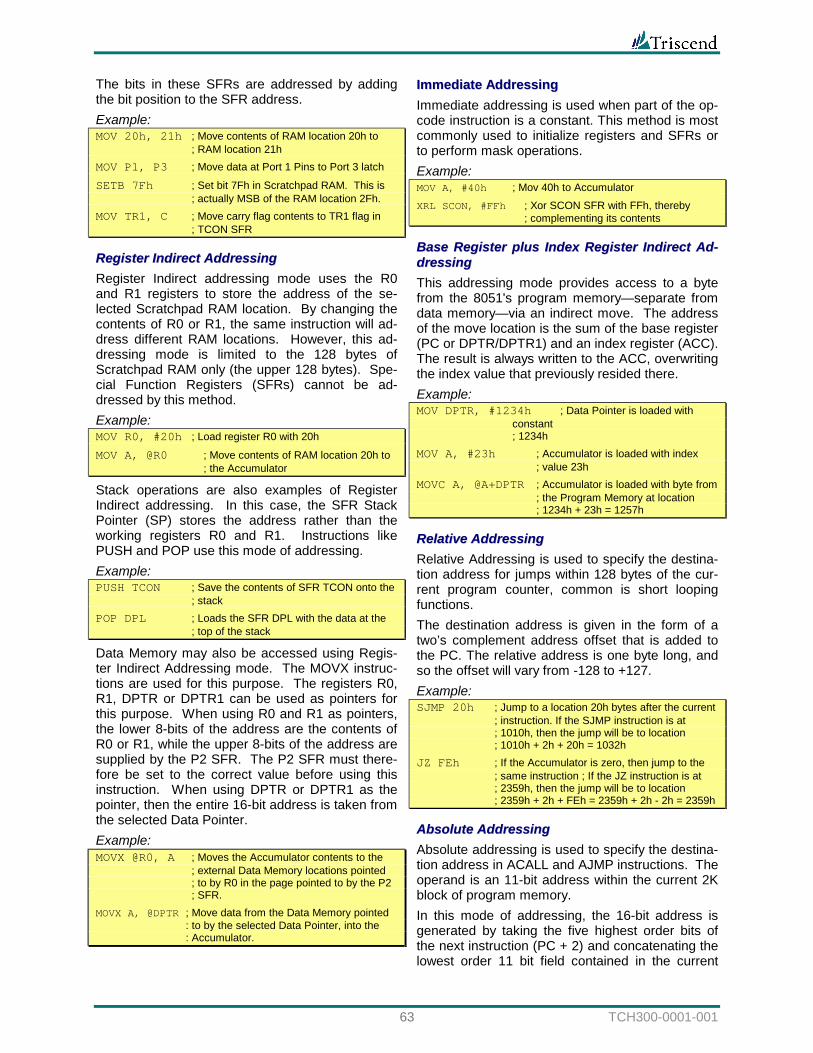
63 TCH300-0001-001
The bits in these SFRs are addressed by adding the bit position to the SFR address. Example: MOV 20h, 21h ; Move contents of RAM location 20h to
; RAM location 21h MOV P1, P3 ; Move data at Port 1 Pins to Port 3 latch
SETB 7Fh ; Set bit 7Fh in Scratchpad RAM. This is ; actually MSB of the RAM location 2Fh.
MOV TR1, C ; Move carry flag contents to TR1 flag in ; TCON SFR
RReeggiisstteerr IInnddiirreecctt AAddddrreessssiinngg Register Indirect addressing mode uses the R0 and R1 registers to store the address of the se-lected Scratchpad RAM location. By changing the contents of R0 or R1, the same instruction will ad-dress different RAM locations. However, this ad-dressing mode is limited to the 128 bytes of Scratchpad RAM only (the upper 128 bytes). Spe-cial Function Registers (SFRs) cannot be ad-dressed by this method. Example: MOV R0, #20h ; Load register R0 with 20h
MOV A, @R0 ; Move contents of RAM location 20h to ; the Accumulator
Stack operations are also examples of Register Indirect addressing. In this case, the SFR Stack Pointer (SP) stores the address rather than the working registers R0 and R1. Instructions like PUSH and POP use this mode of addressing. Example: PUSH TCON ; Save the contents of SFR TCON onto the
; stack POP DPL ; Loads the SFR DPL with the data at the
; top of the stack
Data Memory may also be accessed using Regis-ter Indirect Addressing mode. The MOVX instruc-tions are used for this purpose. The registers R0, R1, DPTR or DPTR1 can be used as pointers for this purpose. When using R0 and R1 as pointers, the lower 8-bits of the address are the contents of R0 or R1, while the upper 8-bits of the address are supplied by the P2 SFR. The P2 SFR must there-fore be set to the correct value before using this instruction. When using DPTR or DPTR1 as the pointer, then the entire 16-bit address is taken from the selected Data Pointer. Example: MOVX @R0, A ; Moves the Accumulator contents to the
; external Data Memory locations pointed ; to by R0 in the page pointed to by the P2 ; SFR.
MOVX A, @DPTR ; Move data from the Data Memory pointed : to by the selected Data Pointer, into the : Accumulator.
IImmmmeeddiiaattee AAddddrreessssiinngg Immediate addressing is used when part of the op-code instruction is a constant. This method is most commonly used to initialize registers and SFRs or to perform mask operations. Example: MOV A, #40h ; Mov 40h to Accumulator XRL SCON, #FFh ; Xor SCON SFR with FFh, thereby
; complementing its contents
BBaassee RReeggiisstteerr pplluuss IInnddeexx RReeggiisstteerr IInnddiirreecctt AAdd--ddrreessssiinngg This addressing mode provides access to a byte from the 8051's program memory—separate from data memory—via an indirect move. The address of the move location is the sum of the base register (PC or DPTR/DPTR1) and an index register (ACC). The result is always written to the ACC, overwriting the index value that previously resided there. Example: MOV DPTR, #1234h ; Data Pointer is loaded with
constant ; 1234h
MOV A, #23h ; Accumulator is loaded with index ; value 23h
MOVC A, @A+DPTR ; Accumulator is loaded with byte from ; the Program Memory at location ; 1234h + 23h = 1257h
RReellaattiivvee AAddddrreessssiinngg Relative Addressing is used to specify the destina-tion address for jumps within 128 bytes of the cur-rent program counter, common is short looping functions. The destination address is given in the form of a two’s complement address offset that is added to the PC. The relative address is one byte long, and so the offset will vary from -128 to +127. Example: SJMP 20h ; Jump to a location 20h bytes after the current
; instruction. If the SJMP instruction is at ; 1010h, then the jump will be to location ; 1010h + 2h + 20h = 1032h
JZ FEh ; If the Accumulator is zero, then jump to the ; same instruction ; If the JZ instruction is at ; 2359h, then the jump will be to location ; 2359h + 2h + FEh = 2359h + 2h - 2h = 2359h
AAbbssoolluuttee AAddddrreessssiinngg Absolute addressing is used to specify the destina-tion address in ACALL and AJMP instructions. The operand is an 11-bit address within the current 2K block of program memory. In this mode of addressing, the 16-bit address is generated by taking the five highest order bits of the next instruction (PC + 2) and concatenating the lowest order 11 bit field contained in the current
Triscend E5 Configurable System-on-Chip Platform
TCH300-0001-001 64
instruction. The resulting addressed location lies within the 2K page of the Program Memory, relative to the first byte of the instruction following the cur-rent instruction. Example: ACALL 0200h ; If the current instruction is at location
; 7FFFh, then a call will be made to the ; location 8200h
LLoonngg AAddddrreessssiinngg Long addressing specifies the full 16-bit address anywhere within the 64K program memory for the LJMP and LCALL instructions. Example: LJMP 8000h ; Jump to location 8000h in program memory.
Interrupts The Triscend E5 has a three priority level interrupt structure with 12 interrupt sources. Each of the interrupt sources has an individual flag, interrupt vector and enable bit. The standard 8051 micro-controller interrupts have individual priority bits. Furthermore, the interrupts—with the exception of the High-Priority Interrupt—can be globally enabled or disabled.
IInntteerrrruupptt SSoouurrcceess The external interrupt sideband signals, INTR0 and INTR1, are either edge triggered or level triggered, depending on bits IT0 and IT1 in the TCON regis-ter. The flag bits IE0 and IE1 in the TCON register generate the interrupt and indicate which interrupt has occurred. When an external interrupt input generates an interrupt, the appropriated flag bit is cleared upon entering the Interrupt Service routine, but only if the interrupt type is edge triggered. In level activated mode, the external requesting source controls the interrupt flag bit rather than the on-chip hardware. For level-triggered interrupts, the IE0 and IE1 flags are not cleared by hardware and must be cleared by the software. The TF0 and TF1 flags generate the Timer 0 and 1 Interrupts. These flags are set when Timer 0 and Timer 1 overflow, respectively. Hardware auto-matically clears the TF0 and TF1 flags when the timer interrupt is serviced. The Timer 2 interrupt is generated by a logical OR of the TF2 and the EXF2 flags. These flags are set by overflow/underflow or capture/reload events in the Timer 2 operation. The hardware does not clear these flags when a Timer 2 interrupt is exe-cuted. Software has to resolve the cause of the interrupt between TF2 and EXF2 and clear the ap-propriate flag. The Watchdog timer can be used as a system monitor or a simple timer. In either case, the
Watchdog timer interrupt flag WDIF (WDCON.3) is set when the time-out count is reached. If the in-terrupt is enabled by the enable bit EIE.4, then an interrupt occurs. The serial port also generates interrupts on data reception or transmission. However, there is only one interrupt source from the Serial block, the logic OR of the RI and TI bits in the SCON SFR. These bits are not automatically cleared by the hardware and the software must clear these bits. The High-Priority Interrupt flag, HPI, (WDCON.4) is set when the HPINT sideband signal is asserted. If this interrupt is enabled then an interrupt occurs. The high-priority interrupt has the highest priority over all the interrupts. The user cannot alter its priority but it can be enabled or disabled via soft-ware. The EHPI bit enables the high-priority inter-rupt. This bit is not controlled by the global inter-rupt enable EA. The standard 8051 interrupt flags that generate interrupts can be set or reset by writing to the ap-propriate registers. Consequently, software can generate interrupts. The addition E5 interrupts (DMA, JTAG, software and hardware breakpoint) can only by reset by software. Individual interrupts can be enabled or disabled by setting or clearing a bit in the IE or the EIE SFR. IE also has a global enable/disable bit, EA, which is cleared to disable all the interrupts at once, except for the high-priority interrupt (HPI), which is unaffected by EA.
PPrriioorriittyy LLeevveell SSttrruuccttuurree There are three priority levels for the interrupts, highest, high and low. The high-priority interrupt HPI has the highest priority. No other interrupt can have this priority. Naturally, a higher priority inter-rupt cannot be interrupted by a lower priority inter-rupt. However there is a predefined hierarchy among the interrupts themselves. This hierarchy helps the interrupt controller to resolve simultane-ous requests having the same priority level. The default hierarchy is defined as shown Table 35. The interrupts are numbered starting from the highest priority to the lowest. Some of the inter-rupts have an individual priority bit that, when set, places those interrupts in a higher-priority category. The default priority remains for interrupts placed in the higher-priority category.
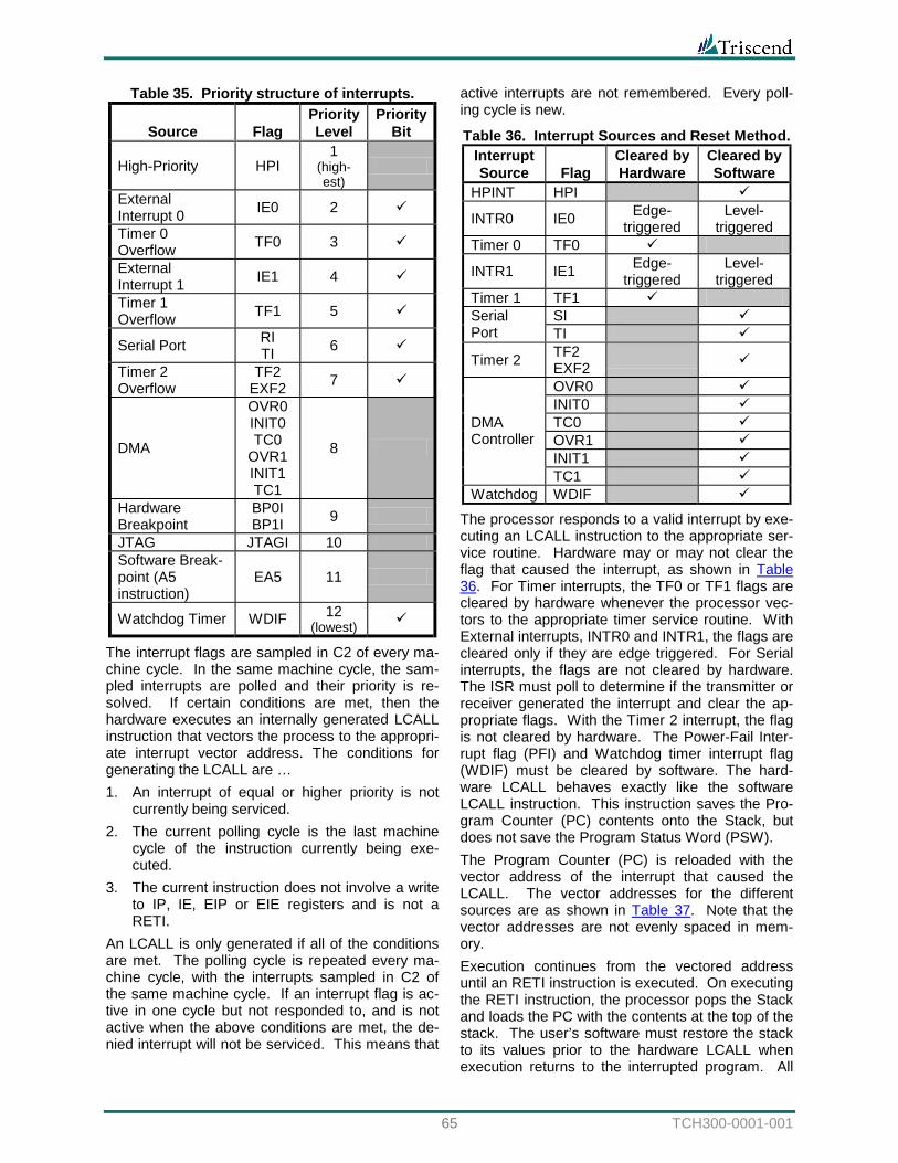
65 TCH300-0001-001
Table 35. Priority structure of interrupts.
Source Flag Priority Level
Priority Bit
High-Priority HPI 1
(high-est)
External Interrupt 0 IE0 2 (
Timer 0 Overflow TF0 3 (
External Interrupt 1 IE1 4 (
Timer 1 Overflow TF1 5 (
Serial Port RI TI 6 (
Timer 2 Overflow
TF2 EXF2 7 (
DMA
OVR0 INIT0 TC0
OVR1 INIT1 TC1
8
Hardware Breakpoint
BP0I BP1I 9
JTAG JTAGI 10 Software Break-point (A5 instruction)
EA5 11
Watchdog Timer WDIF 12 (lowest) (
The interrupt flags are sampled in C2 of every ma-chine cycle. In the same machine cycle, the sam-pled interrupts are polled and their priority is re-solved. If certain conditions are met, then the hardware executes an internally generated LCALL instruction that vectors the process to the appropri-ate interrupt vector address. The conditions for generating the LCALL are … 1. An interrupt of equal or higher priority is not
currently being serviced. 2. The current polling cycle is the last machine
cycle of the instruction currently being exe-cuted.
3. The current instruction does not involve a write to IP, IE, EIP or EIE registers and is not a RETI.
An LCALL is only generated if all of the conditions are met. The polling cycle is repeated every ma-chine cycle, with the interrupts sampled in C2 of the same machine cycle. If an interrupt flag is ac-tive in one cycle but not responded to, and is not active when the above conditions are met, the de-nied interrupt will not be serviced. This means that
active interrupts are not remembered. Every poll-ing cycle is new.
Table 36. Interrupt Sources and Reset Method. Interrupt Source Flag
Cleared by Hardware
Cleared by Software
HPINT HPI (
INTR0 IE0 Edge-triggered
Level-triggered
Timer 0 TF0 (
INTR1 IE1 Edge-triggered
Level-triggered
Timer 1 TF1 ( SI ( Serial
Port TI (
Timer 2 TF2 EXF2 (
OVR0 ( INIT0 ( TC0 ( OVR1 ( INIT1 (
DMA Controller
TC1 ( Watchdog WDIF (
The processor responds to a valid interrupt by exe-cuting an LCALL instruction to the appropriate ser-vice routine. Hardware may or may not clear the flag that caused the interrupt, as shown in Table 36. For Timer interrupts, the TF0 or TF1 flags are cleared by hardware whenever the processor vec-tors to the appropriate timer service routine. With External interrupts, INTR0 and INTR1, the flags are cleared only if they are edge triggered. For Serial interrupts, the flags are not cleared by hardware. The ISR must poll to determine if the transmitter or receiver generated the interrupt and clear the ap-propriate flags. With the Timer 2 interrupt, the flag is not cleared by hardware. The Power-Fail Inter-rupt flag (PFI) and Watchdog timer interrupt flag (WDIF) must be cleared by software. The hard-ware LCALL behaves exactly like the software LCALL instruction. This instruction saves the Pro-gram Counter (PC) contents onto the Stack, but does not save the Program Status Word (PSW). The Program Counter (PC) is reloaded with the vector address of the interrupt that caused the LCALL. The vector addresses for the different sources are as shown in Table 37. Note that the vector addresses are not evenly spaced in mem-ory. Execution continues from the vectored address until an RETI instruction is executed. On executing the RETI instruction, the processor pops the Stack and loads the PC with the contents at the top of the stack. The user’s software must restore the stack to its values prior to the hardware LCALL when execution returns to the interrupted program. All
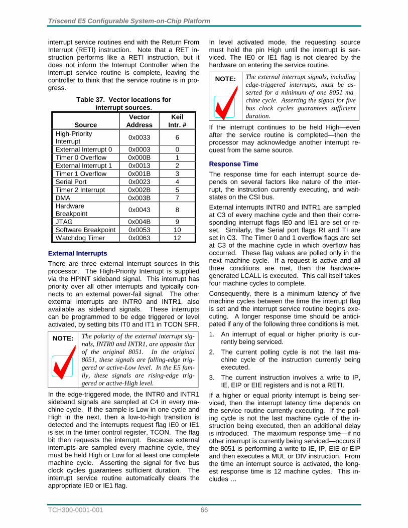
Triscend E5 Configurable System-on-Chip Platform
TCH300-0001-001 66
interrupt service routines end with the Return From Interrupt (RETI) instruction. Note that a RET in-struction performs like a RETI instruction, but it does not inform the Interrupt Controller when the interrupt service routine is complete, leaving the controller to think that the service routine is in pro-gress.
Table 37. Vector locations for interrupt sources.
Source Vector
Address Keil
Intr. # High-Priority Interrupt 0x0033 6
External Interrupt 0 0x0003 0 Timer 0 Overflow 0x000B 1 External Interrupt 1 0x0013 2 Timer 1 Overflow 0x001B 3 Serial Port 0x0023 4 Timer 2 Interrupt 0x002B 5 DMA 0x003B 7 Hardware Breakpoint 0x0043 8
JTAG 0x004B 9 Software Breakpoint 0x0053 10 Watchdog Timer 0x0063 12
EExxtteerrnnaall IInntteerrrruuppttss There are three external interrupt sources in this processor. The High-Priority Interrupt is supplied via the HPINT sideband signal. This interrupt has priority over all other interrupts and typically con-nects to an external power-fail signal. The other external interrupts are INTR0 and INTR1, also available as sideband signals. These interrupts can be programmed to be edge triggered or level activated, by setting bits IT0 and IT1 in TCON SFR.
NOTE:
The polarity of the external interrupt sig-nals, INTR0 and INTR1, are opposite that of the original 8051. In the original 8051, these signals are falling-edge trig-gered or active-Low level. In the E5 fam-ily, these signals are rising-edge trig-gered or active-High level.
In the edge-triggered mode, the INTR0 and INTR1 sideband signals are sampled at C4 in every ma-chine cycle. If the sample is Low in one cycle and High in the next, then a low-to-high transition is detected and the interrupts request flag IE0 or IE1 is set in the timer control register, TCON. The flag bit then requests the interrupt. Because external interrupts are sampled every machine cycle, they must be held High or Low for at least one complete machine cycle. Asserting the signal for five bus clock cycles guarantees sufficient duration. The interrupt service routine automatically clears the appropriate IE0 or IE1 flag.
In level activated mode, the requesting source must hold the pin High until the interrupt is ser-viced. The IE0 or IE1 flag is not cleared by the hardware on entering the service routine.
NOTE:
The external interrupt signals, including edge-triggered interrupts, must be as-serted for a minimum of one 8051 ma-chine cycle. Asserting the signal for five bus clock cycles guarantees sufficient duration.
If the interrupt continues to be held High—even after the service routine is completed—then the processor may acknowledge another interrupt re-quest from the same source.
RReessppoonnssee TTiimmee The response time for each interrupt source de-pends on several factors like nature of the inter-rupt, the instruction currently executing, and wait-states on the CSI bus. External interrupts INTR0 and INTR1 are sampled at C3 of every machine cycle and then their corre-sponding interrupt flags IE0 and IE1 are set or re-set. Similarly, the Serial port flags RI and TI are set in C3. The Timer 0 and 1 overflow flags are set at C3 of the machine cycle in which overflow has occurred. These flag values are polled only in the next machine cycle. If a request is active and all three conditions are met, then the hardware-generated LCALL is executed. This call itself takes four machine cycles to complete. Consequently, there is a minimum latency of five machine cycles between the time the interrupt flag is set and the interrupt service routine begins exe-cuting. A longer response time should be antici-pated if any of the following three conditions is met. 1. An interrupt of equal or higher priority is cur-
rently being serviced. 2. The current polling cycle is not the last ma-
chine cycle of the instruction currently being executed.
3. The current instruction involves a write to IP, IE, EIP or EIE registers and is not a RETI.
If a higher or equal priority interrupt is being ser-viced, then the interrupt latency time depends on the service routine currently executing. If the poll-ing cycle is not the last machine cycle of the in-struction being executed, then an additional delay is introduced. The maximum response time—if no other interrupt is currently being serviced—occurs if the 8051 is performing a write to IE, IP, EIE or EIP and then executes a MUL or DIV instruction. From the time an interrupt source is activated, the long-est response time is 12 machine cycles. This in-cludes …
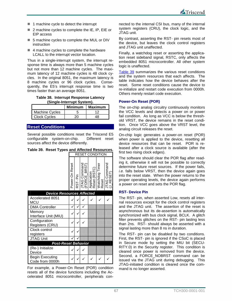
67 TCH300-0001-001
! 1 machine cycle to detect the interrupt ! 2 machine cycles to complete the IE, IP, EIE or
EIP access ! 5 machine cycles to complete the MUL or DIV
instruction ! 4 machine cycles to complete the hardware
LCALL to the interrupt vector location. Thus in a single-interrupt system, the interrupt re-sponse time is always more than 5 machine cycles but not more than 12 machine cycles. The maxi-mum latency of 12 machine cycles is 48 clock cy-cles. In the original 8051, the maximum latency is 8 machine cycles or 96 clock cycles. Conse-quently, the E5’s interrupt response time is two times faster than an average 8051.
Table 38. Interrupt Response Latency (Single-Interrupt System).
Minimum Maximum Machine Cycles 5 12 Clock Cycles 20 48
Reset Conditions Several possible conditions reset the Triscend E5 configurable system-on-chip. Different reset sources affect the device differently.
Table 39. Reset Types and Affected Resources. RESET CONDITION
Pow
er-O
n R
eset
R
ST- P
in
JTAG
Com
man
d (F
OR
CE_
BRST
) Ap
plic
atio
n R
eset
(RST
C)
Wat
chdo
g Ti
mer
R
eset
JT
AG C
omm
and
(J_R
ESET
)
Device Resources Affected Accelerated 8051 MCU ( ( ( ( ( (
DMA Controller ( ( ( Memory Interface Unit (MIU) ( ( (
Configuration Registers (CRU) ( ( (
Clock control registers ( (
JTAG Unit ( ( Post-Reset Behavior
(Re-) Initialize Device ( ( (
Begin Executing Code from 0000h ( ( ( ( ( (
For example, a Power-On Reset (POR) condition resets all of the device functions including the Ac-celerated 8051 microcontroller, peripherals con-
nected to the internal CSI bus, many of the internal system registers (CRU), the clock logic, and the JTAG unit. By contrast, asserting the RST- pin resets most of the device, but leaves the clock control registers and JTAG unit unaffected. Finally, a watchdog reset or asserting the applica-tion reset sideband signal, RSTC, only affects the embedded 8051 microcontroller. All other system logic is unaffected. Table 39 summarizes the various reset conditions and the system resources that each affects. The table indicates how the device behaves after the reset. Some reset conditions cause the device to re-initialize and restart code execution from 0000h. Others merely restart code execution.
PPoowweerr--OOnn RReesseett ((PPOORR)) The on-chip analog circuitry continuously monitors the VCC levels and detects a power on or power fail condition. As long as VCC is below the thresh-old VRST, the device remains in the reset condi-tion. Once VCC goes above the VRST level, the analog circuit releases the reset. On-chip logic generates a power-on reset (POR) when power is applied to the device, resetting all device resources that can be reset. POR is re-leased after a clock source is available (after the first two rising clock edges). The software should clear the POR flag after read-ing it, otherwise it will not be possible to correctly determine future reset sources. If the power fails, i.e. falls below VRST, then the device again goes into the reset state. When the power returns to the proper operating levels, the device again performs a power on reset and sets the POR flag.
RRSSTT-- DDeevviiccee PPiinn The RST- pin, when asserted Low, resets all inter-nal resources except for the clock control registers and the JTAG unit. The assertion of the reset is asynchronous but its de-assertion is automatically synchronized with bus clock signal, BCLK. A glitch filter prevents glitches on the RST- pin lasting less than 2ns. RST- should always be asserted with a signal lasting more than 8 ns in duration. The RST- pin can be disabled by two conditions. First, the RST- pin is ignored if the CSoC is placed in Secure mode by setting the MIU bit (SECU-RITY.0) in the Security register. This condition is cleared once power is removed from the device. Second, a FORCE_NOBRST command can be issued via the JTAG unit during debugging. This JTAG-initiated condition is cleared once the com-mand is no longer asserted.
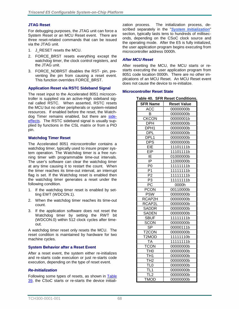
Triscend E5 Configurable System-on-Chip Platform
TCH300-0001-001 68
JJTTAAGG RReesseett For debugging purposes, the JTAG unit can force a System Reset or an MCU Reset event. There are three reset-related commands that can be issued via the JTAG unit. 1. J_RESET resets the MCU. 2. FORCE_BRST resets everything except the
watchdog timer, the clock control registers, and the JTAG unit.
3. FORCE_NOBRST disables the RST- pin, pre-venting the pin from causing a reset event. This function overrides FORCE_BRST.
AApppplliiccaattiioonn RReesseett vviiaa RRSSTTCC SSiiddeebbaanndd SSiiggnnaall The reset input to the Accelerated 8051 microcon-troller is supplied via an active-High sideband sig-nal called RSTC. When asserted, RSTC resets the MCU but no other peripherals or system-related resources. If enabled before the reset, the Watch-dog Timer remains enabled, but there are side-effects. The RSTC sideband signal is usually sup-plied by functions in the CSL matrix or from a PIO pin.
WWaattcchhddoogg TTiimmeerr RReesseett The Accelerated 8051 microcontroller contains a watchdog timer, typically used to insure proper sys-tem operation. The Watchdog timer is a free run-ning timer with programmable time-out intervals. The user’s software can clear the watchdog timer at any time causing it to restart the count. When the timer reaches its time-out interval, an interrupt flag is set. If the Watchdog reset is enabled then the watchdog timer generates a reset under the following condition. 1. If the watchdog timer reset is enabled by set-
ting EWT (WDCON.1). 2. When the watchdog timer reaches its time-out
count. 3. If the application software does not reset the
Watchdog timer by setting the RWT bit (WDCON.0) within 512 clock cycles after time-out.
A watchdog timer reset only resets the MCU. The reset condition is maintained by hardware for two machine cycles.
SSyysstteemm BBeehhaavviioorr aafftteerr aa RReesseett EEvveenntt After a reset event, the system either re-initializes and re-starts code execution or just re-starts code execution, depending on the type of reset event.
RRee--IInniittiiaalliizzaattiioonn Following some types of resets, as shown in Table 39, the CSoC starts or re-starts the device initiali-
zation process. The initialization process, de-scribed separately in the "System Initialization" section, typically lasts tens to hundreds of millisec-onds, depending on the CSoC clock source and the operating mode. After the E5 is fully initialized, the user application program begins executing from microcontroller address 0000h.
AAfftteerr MMCCUU RReesseett After resetting the MCU, the MCU starts or re-starts executing the user application program from 8051 code location 0000h. There are no other im-plications of an MCU Reset. An MCU Reset event does not cause the device to re-initialize.
MMiiccrrooccoonnttrroolllleerr RReesseett SSttaattee
Table 40. SFR Reset Conditions. SFR Name Reset Value
ACC 00000000b B 00000000b
CKCON 00000001b DPH 00000000b DPH1 00000000b DPL 00000000b DPL1 00000000b DPS 00000000b EIE 11101111b EIP 11101111b IE 01000000b IP 11000000b P0 11111111b P1 11111111b P2 11111111b P3 11111111b PC 0000h
PCON 00110000b PSW 00000000b
RCAP2H 00000000b RCAP2L 00000000b SADDR 00000000b SADEN 00000000b SBUF 11111111b SCON 00000000b
SP 00000111b T2CON 00000000b T2MOD 11111110b
TA 11111111b TCON 00000000b TH0 00000000b TH1 00000000b TH2 00000000b TL0 00000000b TL1 00000000b TL2 00000000b
TMOD 00000000b
69 TCH300-0001-001
Most of the SFRs and registers on the device are cleared by reset. The Program Counter is forced to 0000h and is held there as long as the reset condition is applied. The reset state however does not affect the on-chip RAM. The data in the RAM is preserved during the reset. However, the stack pointer is reset to 07h, and therefore the stack con-tents are lost. However, the RAM contents will be lost if the Vcc falls below approximately 2V, as this is the minimum voltage level required for the RAM to operate normally. Therefore, after a first-time power on reset, the RAM contents are indetermi-nate. During a power fail condition, if the power falls below 2V, the RAM contents are lost. After a power on/fail reset, POR = 1, the RAM contents should be assumed lost. When reset, most SFRs are cleared, as shown in Table 40. Interrupts and Timers are disabled. The Watchdog timer is disabled by a Power-On Reset (POR). The WDCON SFR bits are set or cleared in reset condition depending on the source of the reset, as shown in Table 41.
Table 41. Watchdog Timer Reset Values. External
Reset Watchdog
Reset Power-on
Reset WDCON 1x0x0xx0b 1x0x01x0b 11000000b
An 'x' indicates that the reset does not change the bit. The POR bit WDCON.6 is set only by the power on reset. The PFI bit WDCON.4 is set when the power fail condition occurs. However a power-on reset clears this bit if Vcc> Vpfw following the crystal start-up time. The WTRF bit WDCON.2 is set when the Watchdog timer causes a reset. A power-on reset also clears this bit. The EWT bit WDCON.1 is cleared by power-on resets. This dis-ables the Watchdog timer resets. A watchdog or external reset does not affect the EWT bit.
Power Management The Triscend E5 configurable system-on-chip has several features that reduce power consumption, including two power saving modes, Power-Down and Idle. A power-on/power-fail reset guarantees proper start-up or restart operation.
PPoowweerr MMaannaaggeemmeenntt The Triscend E5 configurable system-on-chip has a built-in power-on reset system. This ensures that if the power levels are below the VRST level, the device is forced into the reset state. When power is turned on—such as during a cold reset—the de-vice is reset automatically and remains so as long as VCC is less that VRST. Similarly, when power falls below VRST, the device is automatically reset. This eliminates the need for any external reset cir-cuitry.
PPoowweerr SSaavviinngg The Triscend E5 has two power saving modes of operation, the Power Down mode and the Idle mode. These two modes are possible because the E5 is implemented in fully static CMOS logic. This permits the device to reduce the clock speed to DC. In the most aggressive power down state, where subsystems are properly shut down or blocked, the overall current can be reduced to a typical value of less than 50 µA.
IIddllee MMooddee The Idle mode is primarily provided for compatibility with the original 8051 microcontroller. The device is placed in Idle mode by setting the IDL bit (PCON.0). The instruction that sets the idle bit is the last instruction executed before the device goes into Idle mode. In the Idle mode, the MCU clock is disabled. How-ever, the interrupt controllers, timers, watchdog timer, and serial port continue to operate. Idle mode freezes the MCU state including the Program Counter, the Stack Pointer, the Program Status Word, and the Accumulator. The other registers retain their contents. There are two ways to exit Idle mode. Because the interrupt controller remains active, asserting any enabled interrupt wakes up the processor. This automatically clears the Idle bit, terminates the Idle mode, and executes the appropriate interrupt ser-vice routine (ISR). After the ISR, the program con-tinues to execute from the instruction following the instruction that placed device into Idle mode. An alternate method to exit the Idle mode is by forcing a reset condition. The device is reset by either applying a Low on the external RST- pin, a Power on/fail reset condition, a Watchdog timer reset, or asserting an application reset using the RSTC sideband signal. Some reset conditions cause the Triscend E5 device to re-initialize before re-starting code execution from 0000h. See the "System Initialization" section for more informa-tion. After a reset condition, the program counter is re-set to 0000h and all the SFRs are set to the reset condition. Because the clock is already running, there is no delay and execution starts immediately. In the Idle mode, the Watchdog timer continues to run, and if enabled, a time-out will cause a watch-dog timer interrupt, which will wake up the device. The software must reset the Watchdog timer in order to preempt the reset, which will occur 512 clock periods after the time-out. When the MCU exits from the Idle mode with a reset, the instruc-tion following the one which put the device into Idle mode is not executed.
Triscend E5 Configurable System-on-Chip Platform
TCH300-0001-001 70
PPoowweerr--DDoowwnn MMooddee The device is placed into power-down mode by setting the PCON.1 bit. The instruction that sets this bit is the last instruction executed before the device goes into power-down mode. In power-down mode, all clocks are optionally stopped and internal functions optionally disabled. All activity is completely stopped and the power consumption is reduced to the lowest possible value. The power down control logic optionally prevents the global clock signals from toggling when the MCU powers down. The PWDSEL defines the system behavior when the system enters the power down mode. The MCU is powered down following the execution of an instruction that set the PD flag inside its PCON register. The MCU exits power down by a reset pulse or by responding to an external inter-rupt, as described later. Prior to entering a power down state, the applica-tion program configures PWDSEL with settings that best fits the particular application.
PPoowweerr DDoowwnn SSeelleecctt
- - PIO XTAL OSC GBUF CSLBCLK BCLK
7 6 5 4 3 2 1 0
Mnemonic: PWDSEL Address: FF62h PIO, when set, signals all of the PIO pins when a power-down event occurs. Within each PIO, user-defined values configure the PIO to optionally block inputs by driving a Low value. In addition, the out-put driver is optionally three-stated, turning on the weak-follower feature. The individual PIO controls are loaded during device initialization. XTAL, when set, blocks the external oscillator dur-ing power down mode. BCLK is frozen in its High state. Note that the memory interface unit (MIU) must be set up correctly to properly exit power down mode, as described later. OSC, when set, shuts off the internal oscillator dur-ing power down mode. GBUF, when set, signals the six global buffers when a power-down event occurs. Each global buffer has individual control bits that define its be-havior during a power down or breakpoint event. CSL_BCLK, when set, blocks the bus clock into the configurable system logic (CSL) matrix during power-down mode. BCLK, when set, blocks the bus clock during power-down mode. Power down mode is initiated by writing a “1” to the power down bit in the microcontroller’s PCON SFR. Depending on what portions of the device are se-lected for shut down or blocking, the effect is im-
mediate. However, special attention is required when exiting power down mode after shutting off the crystal oscillator.
PPoowweerr--OOnn RReesseett CCoonnttrrooll
- - - - - - - PORCT
7 6 5 4 3 2 1 0
Mnemonic: PORCTRL Address: FF63h PORCT, when set, disables the Power-On Reset (POR) circuitry during power-down mode. Clearing this bit keeps the POR circuitry active. Power down mode is initiated by writing a “1” to the power down bit in the microcontroller’s PCON SFR.
SShhuuttttiinngg DDoowwnn tthhee CCrryyssttaall OOsscciillllaattoorr If the external crystal is selected to drive the inter-nal system clock (BCLK), it can be shut down dur-ing power-down by setting the XTAL bit. However, if the crystal oscillator is shut down, the device automatically selects the internal ring oscillator as the default clock source upon exiting power down mode. Consequently, if the user program fetches instructions via the MIU when leaving power down—the usual case—potential timing problems could occur if the frequency of the internal ring os-cillator is greater than the frequency of the external crystal. Before entering power down mode, the user application code must properly configure the MIU’s external memory timing with values that are more conservative. See Table 42 for more details.
RReessttaarrttiinngg tthhee CCrryyssttaall OOsscciillllaattoorr aafftteerr EExxiittiinngg PPoowweerr--DDoowwnn MMooddee If the crystal oscillator is disabled during power down, then the internal ring oscillator becomes the clock source for the bus clock, BCLK. Before switching back to the crystal oscillator, the user program must wait for the crystal oscillator to stabilize. This can be accomplished either by a software timing loop or by using one of the MCU timers. Once the necessary time has elapsed, the user program must switch back to the external crystal and set the MIU read timing parameters to the pre-power-down values. Table 42 summarizes the sequence for entering and exiting power down mode, when turning off the crystal oscillator during power-down mode. The method used depends on the crystal frequency. With the crystal shut off, the device wakes from power-down mode using the internal ring oscillator. The sequences in Table 42 represent the cases where the crystal is faster and slower than the in-ternal ring oscillator. The registers accessed in Table 42 are MIUCTRL and MISC. MIUCTRL controls the MIU timing and MISC contains the clock select bit. These registers
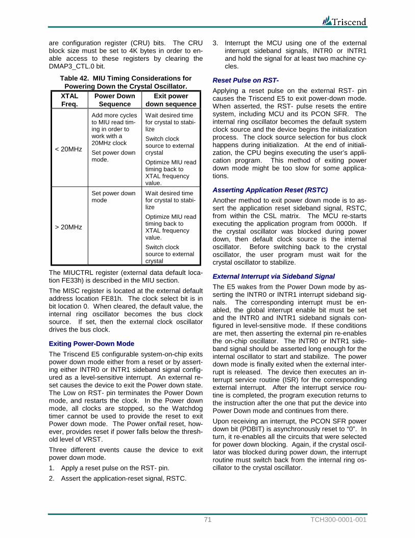
71 TCH300-0001-001
are configuration register (CRU) bits. The CRU block size must be set to 4K bytes in order to en-able access to these registers by clearing the DMAP3_CTL.0 bit.
Table 42. MIU Timing Considerations for Powering Down the Crystal Oscillator.
XTAL Freq.
Power Down Sequence
Exit power down sequence
< 20MHz
Add more cycles to MIU read tim-ing in order to work with a 20MHz clock Set power down mode.
Wait desired time for crystal to stabi-lize Switch clock source to external crystal Optimize MIU read timing back to XTAL frequency value.
> 20MHz
Set power down mode
Wait desired time for crystal to stabi-lize Optimize MIU read timing back to XTAL frequency value. Switch clock source to external crystal
The MIUCTRL register (external data default loca-tion FE33h) is described in the MIU section. The MISC register is located at the external default address location FE81h. The clock select bit is in bit location 0. When cleared, the default value, the internal ring oscillator becomes the bus clock source. If set, then the external clock oscillator drives the bus clock.
EExxiittiinngg PPoowweerr--DDoowwnn MMooddee The Triscend E5 configurable system-on-chip exits power down mode either from a reset or by assert-ing either INTR0 or INTR1 sideband signal config-ured as a level-sensitive interrupt. An external re-set causes the device to exit the Power down state. The Low on RST- pin terminates the Power Down mode, and restarts the clock. In the Power down mode, all clocks are stopped, so the Watchdog timer cannot be used to provide the reset to exit Power down mode. The Power on/fail reset, how-ever, provides reset if power falls below the thresh-old level of VRST. Three different events cause the device to exit power down mode. 1. Apply a reset pulse on the RST- pin. 2. Assert the application-reset signal, RSTC.
3. Interrupt the MCU using one of the external interrupt sideband signals, INTR0 or INTR1 and hold the signal for at least two machine cy-cles.
RReesseett PPuullssee oonn RRSSTT-- Applying a reset pulse on the external RST- pin causes the Triscend E5 to exit power-down mode. When asserted, the RST- pulse resets the entire system, including MCU and its PCON SFR. The internal ring oscillator becomes the default system clock source and the device begins the initialization process. The clock source selection for bus clock happens during initialization. At the end of initiali-zation, the CPU begins executing the user’s appli-cation program. This method of exiting power down mode might be too slow for some applica-tions.
AAsssseerrttiinngg AApppplliiccaattiioonn RReesseett ((RRSSTTCC)) Another method to exit power down mode is to as-sert the application reset sideband signal, RSTC, from within the CSL matrix. The MCU re-starts executing the application program from 0000h. If the crystal oscillator was blocked during power down, then default clock source is the internal oscillator. Before switching back to the crystal oscillator, the user program must wait for the crystal oscillator to stabilize.
EExxtteerrnnaall IInntteerrrruupptt vviiaa SSiiddeebbaanndd SSiiggnnaall The E5 wakes from the Power Down mode by as-serting the INTR0 or INTR1 interrupt sideband sig-nals. The corresponding interrupt must be en-abled, the global interrupt enable bit must be set and the INTR0 and INTR1 sideband signals con-figured in level-sensitive mode. If these conditions are met, then asserting the external pin re-enables the on-chip oscillator. The INTR0 or INTR1 side-band signal should be asserted long enough for the internal oscillator to start and stabilize. The power down mode is finally exited when the external inter-rupt is released. The device then executes an in-terrupt service routine (ISR) for the corresponding external interrupt. After the interrupt service rou-tine is completed, the program execution returns to the instruction after the one that put the device into Power Down mode and continues from there. Upon receiving an interrupt, the PCON SFR power down bit (PDBIT) is asynchronously reset to “0”. In turn, it re-enables all the circuits that were selected for power down blocking. Again, if the crystal oscil-lator was blocked during power down, the interrupt routine must switch back from the internal ring os-cillator to the crystal oscillator.
Triscend E5 Configurable System-on-Chip Platform
TCH300-0001-001 72
Glossary CSoC - Configurable System-on-Chip. A configur-able device containing a dedicated processor, con-figurable logic, on-chip RAM, and a dedicated in-ternal bus. CRU - Configuration Register Unit. Registers that define special functions on the Triscend E5 device. CSL - Configurable System Logic. The peripheral configurable logic matrix providing user-programmable functions to the microcontroller and its peripherals. CSI - Configurable System Interconnect. The on-chip bus that bridges the Configurable System Logic (CSL) matrix, the Accelerated 8051 micro-controller, the dedicated peripherals, and the Memory Interface Unit (MIU). DMA - Direct Memory Access. A controller that offloads memory and I/O transfers from the micro-controller. JTAG - Joint Test Action Group. A general name given to the four-wire serial interface described in IEEE 1149.1. MCU - Microcontroller Unit. The Accelerated 8051 microcontroller embedded within the Triscend E5 configurable system-on-chip. MIU - Memory Interface Unit. Connects the micro-controller, its peripherals, and the internal system bus to external memory resources. PIO - Programmable Input/Output. SFR - Special Function Register. An 8051-based term for registers that control the microcontrollers peripheral functions.
Life Support Policy Triscend's products are not authorized for use as critical components in life support devices or sys-tems unless a specific written agreement pertaining to such intended use is executed between the manufacturer and the President of Triscend. 1. Life support devices or systems are devices
which (a) are intended for surgical implant into the body or (b) support or sustain life and whose failure to perform, when properly used in accordance with instructions for use pro-vided in the labeling, can be reasonably ex-pected to result in significant injury to the user.
2. Critical component in any component of a life support device or system whose failure to per-form can be reasonably expected to cause the failure of the life support device system, or af-fect its safety or effectiveness.
Revision List
VVeerrssiioonn 11..0055 ttoo 11..0066 ! Added text to JTAG Reset stating that the
watchdog timer is not reset by a FORCE_BRST command.
! Corrected 208-pin PQFP package footprint drawing to remove N.C. pins for TE502. The TE502 is not offered in this package.
! Added Appendix A: E5 Instruction Timing. ! Added note on side-effects of a MCU reset on
the Watchdog Timer.
VVeerrssiioonn 11..0044 ttoo 11..0055 ! Added highlighting to show hyperlinks in docu-
ment. ! Further clarified that WAITNEXT signal always
asserts wait-states on the following bus cycle, independent of other logic. See WAITNEXT (input to bus socket).
! Added power-down and power consumption information. See Triscend E5 Power/Current Consumption Characteristics.
! Added additional information on how to connect PMOD/A31, VSYS, SLAVE-, and RST- pins in typical applications. See Pin Description.
! Added production pin-to-pin timing information for all devices. See Pin-to-Pin Guaranteed Timing Specifications.
! Changed the term “8032 ‘Turbo’ microcontrol-ler” to “Accelerated 8051 microcontroller” throughout the document. Many developers are not familiar with the 8032 device number. The 8032 is a ROM-less version of the 8052, which is a superset of the 8051. Generally changed all references from 8032 to 8051.
! Added a note about how long to assert side-band interrupt signals. See second note in External Interrupts.
! Corrected obsolete figure numbers throughout the Triscend E5 Switching Characteristic Guidelines section.
! Added Unique Technologies as an authorized Triscend distributor in North America. See
73 TCH300-0001-001
U.S. Distribution. ! Removed duplicated paragraph under Priority
Level Structure. ! Corrected values for Bus Clock, Input Set-Up
and Hold. The –25 and –40 speed grade val-ues were swapped.
! Clarified text to show that TMDRZ is a hold time and correctly defined it as a minimum specifica-tion value. See Memory Interface Unit (MIU) Timing Characteristic Guidelines, Stand-alone Operation (SLAVE- = High).
! Removed maximum specification on TMZOE as it is not required. Data is captured by the bus clock. The OE- pin is also controlled by the same bus clock edge. The hold time is actually negative, relative to OE-, but is specified as zero. See Asynchronous Memory Interface Timing.
VVeerrssiioonn 11..0033 ttoo 11..0044 ! Added Triscend E5 Switching Characteristic
Guidelines section. ! Removed 208-pin PQFP as a package option
for the TE502. Affects Table 45, 208-pin PQFP Package Footprint, top view drawing, 208-pin PQFP Package Pinout Tables, and 208-pin PQFP Package Pins by Type.
! Added information on 484-ball BGA package. ! Added notes 2 through 7 to Electrical and Tim-
ing Characteristics page. ! Added TTL output current specifications to
Recommended Operating Conditions/DC Characteristics.
! Added 128-pin and 208-pin PQFP Package Land Pattern Dimensions.
! Provided additional details on output drive cur-rent. See Table 14.
! Added additional description to VSYS pin.
VVeerrssiioonn 11..0022 ttoo 11..0033 ! Corrected the address for the MISC register in
text. The correct location is 0xfe81. ! Corrected a typo in the zip code for Triscend's
mailing address. ! Updated hyper-links to Triscend sales office
and international representatives. ! Updated the E-mail address for Triscend.
VVeerrssiioonn 11..0000 ttoo 11..0022 ! Updated specification for TE512 device to re-
flect SRAM size change from 16K bytes to 32K bytes. Change affects Table 1, Table 20, chart
under Ordering Information, and the 128-pin and 208-pin package pinout drawings.
! Corrected polarity of input signals during power-down. Correct value is Low. Affects description of PIO bit in the Power Down Select register and Input Options for the PIO low-power mode.
! Added a register description for the 8051's B register SFR. See B Register.
! Added information about pin directionality during initialization to Pin Description.
! Added additional information on the VSYS and SLAVE- pins to Pin Description.
! Added information on using TH1 to control the baud rate for the serial port. See Timer 1 MSB.
! Added information on using RCAP2H and RCAP2L to control the baud rate for the serial port. See Timer 2 Capture LSB and Timer 2 Capture MSB.
! Added details to 5-volt tolerant PIO support. See 5-Volt Tolerant I/Os.
! Updated PIO drawing to reflect proper location of inversion multiplexer on output and output-enable signal paths, as shown in Figure 27.
! Added additional detail on how the CSI bus re-sources operate. See Configurable System Interconnect (CSI) Bus.
! Added information on how a Selector can ad-dress an external peripheral connected to the MIU bus. See Figure 13 and External Memory Request Mode.
! Added debugging support requirements. See Debugging Support System Requirements.
! Added phrase about using the internal feedback resistor when using the internal crystal oscillator amplified. See System clock select (BCLK).
! Corrected the direction of the inverting buffer for the crystal oscillator amplified in Figure 44.
! The largest ball-grid array packaged changed to a 484-ball BGA package. Affects Table 44, Table 45, Ordering Information, and the pre-vious BGA pinout diagrams and pinout tables were removed from this version.
! Renamed sideband signals INT0, INT1 to INTR0, INTR1 to be consistent with FastChip naming.
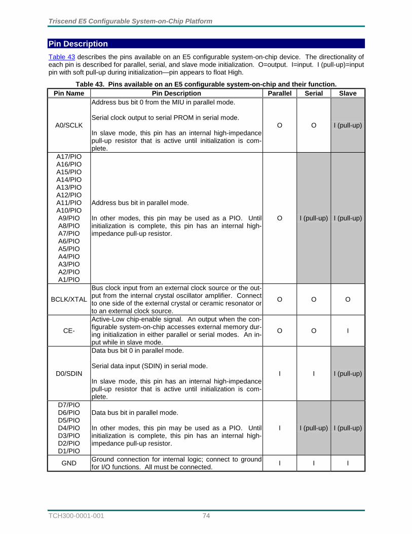
Triscend E5 Configurable System-on-Chip Platform
TCH300-0001-001 74
Pin Description Table 43 describes the pins available on an E5 configurable system-on-chip device. The directionality of each pin is described for parallel, serial, and slave mode initialization. O=output. I=input. I (pull-up)=input pin with soft pull-up during initialization—pin appears to float High.
Table 43. Pins available on an E5 configurable system-on-chip and their function. Pin Name Pin Description Parallel Serial Slave
A0/SCLK
Address bus bit 0 from the MIU in parallel mode. Serial clock output to serial PROM in serial mode. In slave mode, this pin has an internal high-impedance pull-up resistor that is active until initialization is com-plete.
O O I (pull-up)
A17/PIO A16/PIO A15/PIO A14/PIO A13/PIO A12/PIO A11/PIO A10/PIO A9/PIO A8/PIO A7/PIO A6/PIO A5/PIO A4/PIO A3/PIO A2/PIO A1/PIO
Address bus bit in parallel mode. In other modes, this pin may be used as a PIO. Until initialization is complete, this pin has an internal high-impedance pull-up resistor.
O I (pull-up) I (pull-up)
BCLK/XTAL
Bus clock input from an external clock source or the out-put from the internal crystal oscillator amplifier. Connect to one side of the external crystal or ceramic resonator or to an external clock source.
O O O
CE-
Active-Low chip-enable signal. An output when the con-figurable system-on-chip accesses external memory dur-ing initialization in either parallel or serial modes. An in-put while in slave mode.
O O I
D0/SDIN
Data bus bit 0 in parallel mode. Serial data input (SDIN) in serial mode. In slave mode, this pin has an internal high-impedance pull-up resistor that is active until initialization is com-plete.
I I I (pull-up)
D7/PIO D6/PIO D5/PIO D4/PIO D3/PIO D2/PIO D1/PIO
Data bus bit in parallel mode. In other modes, this pin may be used as a PIO. Until initialization is complete, this pin has an internal high-impedance pull-up resistor.
I I (pull-up) I (pull-up)
GND Ground connection for internal logic; connect to ground for I/O functions. All must be connected. I I I
75 TCH300-0001-001
Pin Name Pin Description Parallel Serial Slave
GNDIO Ground connection for I/O functions; connect to ground for internal logic. All must be connected. I I I
N.C. No connect. There is no function on this pin. N.C. N.C. N.C.
OE-/SRST
Active-Low output-enable signal. An output when the configurable system-on-chip accesses external memory during initialization in parallel or serial modes. An input while in slave mode.
O O I
PIO
General-purpose input, output, or bi-directional signal pin after initialization is complete. Before initialization is complete, these pins have internal high-impedance pull-up resistors that pull the signal pin to a High logic level.
I (pull-up) I (pull-up) I (pull-up)
PIO/A18 PIO/A19 PIO/A20 PIO/A21 PIO/A22 PIO/A23 PIO/A24 PIO/A25 PIO/A26 PIO/A27 PIO/A28 PIO/A29 PIO/A30
Typically, a general-purpose input, output, or bi-directional signal pin after initialization is complete. Be-fore initialization is complete, this pin has an internal high-impedance pull-up resistor that pulls the signal pin to a High logic level. Also used in multi-chip mode to expand the upper address bits for external accesses.
I (pull-up) I (pull-up) I (pull-up)
PIO/GBUF5 PIO/GBUF4 PIO/GBUF3 PIO/GBUF2 PIO/GBUF1 PIO/GBUF0
Global buffer input. Typically, a general-purpose input, output, or bi-directional signal pin after initialization is complete. Before initialization is complete, this pin has an internal high-impedance pull-up resistor that pull the signal pin to a High
I (pull-up) I (pull-up) I (pull-up)
PIO/XDONE
Typically, a general-purpose input, output, or bi-directional signal pin after initialization is complete. Be-fore initialization is complete, this pin has an internal high-impedance pull-up resistor that pulls the signal pin to a High logic level. If SLAVE-=Low, then used in multi-chip mode to for inter-device transfer handshaking.
I (pull-up) I (pull-up) I (pull-up)
PMOD/PIO/ A31
Tied Low during initialization to indicate serial mode. Left floating or pulled High during initialization for parallel mode. Also a potential general-purpose input, output, or bi-directional signal pin after initialization is complete but with the restrictions described above. Before initialization is complete, this pin has an internal high-impedance pull-up resistor that pulls the signal pin to a High logic level. Also used in multi-chip mode to expand the upper ad-dress bits for external accesses.
Optionally pull High using a pull-up resistor
I (pull-up)
Pull Low using a
pull-down resistor
I (pull-up)
I (pull-up)
RST- Device reset input. Active Low. Pull High if unused. I I I
SLAVE-
Slave mode input. Active Low. Tie High for most appli-cations indicating that the CSoC device initializes itself from an external PROM, either parallel or serial. Tie Low if another processor initializes the CSoC device via the MIU interface. This pin must be connected. Do not allow it to float.
Tie High (I)
Tie High (I)
Tie Low (I)
TCK JTAG Test Clock input. Tie High if unused. I I I TDI JTAG Test Data Input. Tie High if unused. I I I TDO JTAG Test Data Output. O O O TMS JTAG Test Mode Select input. Tie High if unused. I I I
Triscend E5 Configurable System-on-Chip Platform
TCH300-0001-001 76
Pin Name Pin Description Parallel Serial Slave
VCC
Supply voltage for internal logic functions, separate from I/O. Connect to a +3.3 volt supply. All must be con-nected and each must be decoupled with a 0.01 to 0.1 µF capacitor to ground.
I I I
VCCIO
Supply voltage for I/O functions, separate from internal logic. Connect to a +3.3 volt supply. All must be con-nected and each must be decoupled with a 0.01 to 0.1 µF capacitor to ground.
I I I
VSYS
External 'system voltage-good' indicator input. Indicates when external devices have sufficient operating voltage. In most applications, connect VSYS to VCCIO supply source or to a "Power Good" output from the system power supply. If VSYS is High during initialization and no valid configuration is found, the CSoC device automati-cally powers down to conserve power. If VSYS is Low, the CSoC device attempts to initialize itself until it finds valid initialization data. This pin must be connected. Do not allow it to float.
Always connect
(I)
Always connect
(I)
Always connect
(I)
WE-/SEN-
Active-Low write-enable signal typically used to program external FLASH-based devices. An output when the E5 accesses external memory during initialization in parallel or serial modes. An input while in slave mode.
O O I
XTALIN
The input from the external crystal into the internal crystal oscillator amplifier. Connect to one side of the external crystal or ceramic resonator. Leave unconnected if not using an external crystal or resonator.
I I I
Pinout Diagrams and Tables
AAvvaaiillaabbllee PPaacckkaaggeess aanndd PPaacckkaaggee CCooddeess Each Triscend E5 family member is available in different packages. Each ordering code contains a letter defining the package style, as shown in Table 44.
Table 44. Package Codes. Package
Code Package
Type L 128-pin PQFP Q 208-pin PQFP B 484-ball BGA
FFoooottpprriinntt--CCoommppaattiibbiilliittyy Each Triscend E5 configurable system-on-chip is designed to be footprint compatibly with other E5 family members available in the same package, providing additional design and manufacturing flexibility. A designer can easily select a larger or more cost-effective E5 device that fits a pre-existing printed circuit board (PCB) design. Though the Triscend E5 and A7 families are avail-able in similar package options, the E5 and A7 families are not pin compatible with one another.
AAvvaaiillaabbllee PPIIOOss bbyy PPaacckkaaggee The number of user-configurable PIO pins depends on the base device type and the package in which it is packaged. Table 45 shows the available PIOs by package style. Two values are indicated for each device type, one for parallel mode and one for serial mode configuration. Both cases assume that the upper address bits, A[31:18] are used as PIOs, which is the default case.
Table 45. Available PIOs by Package Device Mode LQ128 PQ208 BG484
Parallel 52 E502 Serial 76
Parallel 60 100 E505 Serial 84 124 Parallel 60 126 E512 Serial 84 150
Parallel 126 228 E520 Serial 150 252 Parallel 126 292 E532 Serial
150 316
77 TCH300-0001-001
112288--ppiinn TThhiinn PPQQFFPP FFoooottpprriinntt,, ttoopp vviieeww
VCC
IO
GN
DIO
A17
/PIO
A16
/PIO
A15
/PIO
A14
/PIO
A13
/PIO
A12
/PIO
VCC
IOA
11/P
IOA
10/P
IOA
9/PI
OA
8/PI
OG
ND
128
VCC
127
GN
DIO
126
125
124
123
122
PIO
121
PIO
120
A7/
PIO
119
GN
DIO
118
117
116
115
114
113
112
A6/
PIO
111
110
109
108
107
106
105
104
GN
DIO
A5/
PIO
A4/
PIO
A3/
PIO
A2/
PIO
103
102
101
100
99 98A
1/PI
O
97A
0/SC
LK
PIO
PIO
PIO
PIO
VCCIO
89
88
87
D3/PIO
RST-
79
78
D7/PIO
77
GNDIO
76
D5/PIO
75
D4/PIO
74
GND
73
VCC
72
71
D2/PIO
70
69
68PIO
67PIO
66D1/PIO
65D0/SDIN
D6/PIO
GNDIO
86
85
CE-
84
OE-/SRST
83
82 GNDIO81
80
PIO/XDONE
PIO (N.C.)
WE-/SEN-SLAVE-
96
94
93
92
91
90
PIOPIO
PIO (N.C.)PIO (N.C.)
VCCIO
PIO (N.C.)PIO
GNDIO
VSYS9533
PIO
34
PIO
35
PIO
36
PIO
/GB
UF5
37
PIO
38
PIO
39
PIO
40
PIO
/GB
UF4
41
GN
DIO
42
VCC
43
GN
D
44 45 46 47 48
PIO
49PI
O/G
BU
F3
50 51
GN
DIO
52
PIO
/GB
UF2
53
PIO
54
PIO
55
PIO
56
PIO
57
VCC
IOPIO
PIO
/GB
UF1
PIO
/GB
UF0
GN
DIO
58 59 60 61
GN
DIO
62 63
PIO
64
PIO
VCC
IOPIO
PIO
PIO
PIO
1
XTALIN 2
BCLK/XTAL 3
4
GNDIO
5
PIO/A26
6
PIO/A27
7
TDI
8
TDO
9
GNDIO 10
(N.C.) PIO
11
PIO 12
TCK
13
TMS
14
15
(N.C.) PIO 16
PIO/A23
17VCCIO18
PIO/A22 19
PIO
20
PIO/A24 21
PIO/A25 22
PIO/A18
23
PIO/A19
24
25
PIO/A20PIO/A21
GNDIO
PIO/A29PIO/A30
(N.C.) PIO 26
(N.C.) PIO 27
PIO/A28 28
29
30
31
GNDIO
VCCIO 32PMOD/PIO/A31
TE502S08L
TE505S16L
TE512S32L
(N.C.) indicates a pin that is not connected on the TE502S08L device in this package.
Triscend E5 Configurable System-on-Chip Platform
TCH300-0001-001 78
112288--ppiinn TThhiinn PPQQFFPP PPaacckkaaggee PPiinnoouutt TTaabblleess Shaded cells represent a pin that is not connected on the TE502 device but is a PIO pin for all other de-vices.
Pin TE502 TE505 TE512
1 GNDIO GNDIO 2 XTALIN XTALIN 3 BCLK/XTAL BCLK/XTAL 4 TDI TDI 5 TDO TDO 6 TCK TCK 7 TMS TMS 8 PIO/A18 PIO/A18 9 PIO/A19 PIO/A19
10 GNDIO GNDIO 11 PIO PIO 12 PIO PIO 13 PIO/A20 PIO/A20 14 PIO/A21 PIO/A21 15 N.C. PIO 16 N.C. PIO 17 VCCIO VCCIO 18 GNDIO GNDIO 19 PIO/A22 PIO/A22 20 PIO/A23 PIO/A23 21 PIO/A24 PIO/A24 22 PIO/A25 PIO/A25 23 PIO/A26 PIO/A26 24 PIO/A27 PIO/A27 25 GNDIO GNDIO 26 N.C. PIO 27 N.C. PIO 28 PIO/A28 PIO/A28 29 PIO/A29 PIO/A29 30 PIO/A30 PIO/A30
31 PMOD/PIO/ A31
PMOD/PIO/ A31
32 VCCIO VCCIO 33 GNDIO GNDIO 34 PIO PIO 35 PIO PIO 36 PIO PIO 37 PIO/GBUF5 PIO/GBUF5 38 GNDIO GNDIO 39 PIO PIO 40 PIO PIO 41 PIO PIO 42 PIO/GBUF4 PIO/GBUF4 43 PIO PIO 44 PIO PIO 45 VCC VCC 46 GND GND 47 PIO PIO
Pin TE502 TE505 TE512
48 PIO/GBUF3 PIO/GBUF3 49 GNDIO GNDIO 50 PIO/GBUF2 PIO/GBUF2 51 PIO PIO 52 VCCIO VCCIO 53 PIO PIO 54 PIO PIO 55 PIO PIO 56 PIO/GBUF1 PIO/GBUF1 57 GNDIO GNDIO 58 PIO PIO 59 PIO PIO 60 PIO PIO 61 PIO/GBUF0 PIO/GBUF0 62 PIO PIO 63 PIO PIO 64 VCCIO VCCIO 65 GNDIO GNDIO 66 D0/SDIN D0/SDIN 67 D1/PIO D1/PIO 68 PIO PIO 69 PIO PIO 70 PIO PIO 71 PIO PIO 72 GNDIO GNDIO 73 N.C. PIO 74 N.C. PIO 75 D2/PIO D2/PIO 76 D3/PIO D3/PIO 77 VCC VCC 78 GND GND 79 D4/PIO D4/PIO 80 D5/PIO D5/PIO 81 VCCIO VCCIO 82 GNDIO GNDIO 83 D6/PIO D6/PIO 84 D7/PIO D7/PIO 85 N.C. PIO 86 N.C. PIO 87 PIO PIO 88 PIO/XDONE PIO/XDONE 89 GNDIO GNDIO 90 WE-/SEN- WE-/SEN- 91 SLAVE- SLAVE- 92 OE-/SRST OE-/SRST 93 CE- CE- 94 RST- RST- 95 VSYS VSYS
Pin TE502 TE505 TE512
96 VCCIO VCCIO 97 GNDIO GNDIO 98 A0/SCLK A0/SCLK 99 A1/PIO A1/PIO
100 A2/PIO A2/PIO 101 A3/PIO A3/PIO 102 GNDIO GNDIO 103 A4/PIO A4/PIO 104 A5/PIO A5/PIO 105 A6/PIO A6/PIO 106 A7/PIO A7/PIO 107 PIO PIO 108 PIO PIO 109 GNDIO GNDIO 110 VCC VCC 111 GND GND 112 A8/PIO A8/PIO 113 A9/PIO A9/PIO 114 A10/PIO A10/PIO 115 A11/PIO A11/PIO 116 VCCIO VCCIO 117 PIO PIO 118 PIO PIO 119 A12/PIO A12/PIO 120 A13/PIO A13/PIO 121 GNDIO GNDIO 122 PIO PIO 123 PIO PIO 124 A14/PIO A14/PIO 125 A15/PIO A15/PIO 126 A16/PIO A16/PIO 127 A17/PIO A17/PIO 128 VCCIO VCCIO
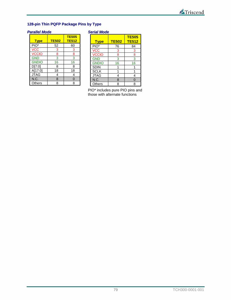
79 TCH300-0001-001
112288--ppiinn TThhiinn PPQQFFPP PPaacckkaaggee PPiinnss bbyy TTyyppee
PPaarraalllleell MMooddee
Type TE502 TE505 TE512
PIO* 52 60 VCC 3 3 VCCIO 8 8 GND 3 3 GNDIO 16 16 D[7:0] 8 8 A[17:0] 18 18 JTAG 4 4 N.C. 8 0 Others 8 8
SSeerriiaall MMooddee
Type TE502 TE505 TE512
PIO* 76 84 VCC 3 3 VCCIO 8 8 GND 3 3 GNDIO 16 16 SDIN 1 1 SCLK 1 1 JTAG 4 4 N.C. 8 0 Others 8 8
PIO* includes pure PIO pins and those with alternate functions
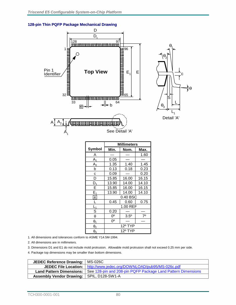
Triscend E5 Configurable System-on-Chip Platform
TCH300-0001-001 80
112288--ppiinn TThhiinn PPQQFFPP PPaacckkaaggee MMeecchhaanniiccaall DDrraawwiinngg
1
32
33 64
65
96
97128
Pin 1Identifier
D1
D
EE1Top View
e b
A A2
A1See Detail 'A'
θ2
θ1
θ3
L1
L
θ
c
Detail 'A'
S
Millimeters Symbol Min. Nom. Max.
A — — 1.60 A1 0.05 — — A2 1.35 1.40 1.45 b 0.13 0.18 0.23 c 0.09 — 0.20 D 15.85 16.00 16.15 D1 13.90 14.00 14.10 E 15.85 16.00 16.15 E1 13.90 14.00 14.10 e 0.40 BSC L 0.45 0.60 0.75 L1 1.00 REF S 0.20 — — θ 0º 3.5º 7º θ1 0º — — θ2 12º TYP θ3 12º TYP
1. All dimensions and tolerances conform to ASME Y14.5M-1994. 2. All dimensions are in millimeters. 3. Dimensions D1 and E1 do not include mold protrusion. Allowable mold protrusion shall not exceed 0.25 mm per side. 4. Package top dimensions may be smaller than bottom dimensions.
JEDEC Reference Drawing: MS-026C JEDEC File Location: http://www.jedec.org/DOWNLOAD/pub95/MS-026c.pdf
Land Pattern Dimensions: See 128-pin and 208-pin PQFP Package Land Pattern Dimensions Assembly Vendor Drawing: SPIL, D128-SW1-A
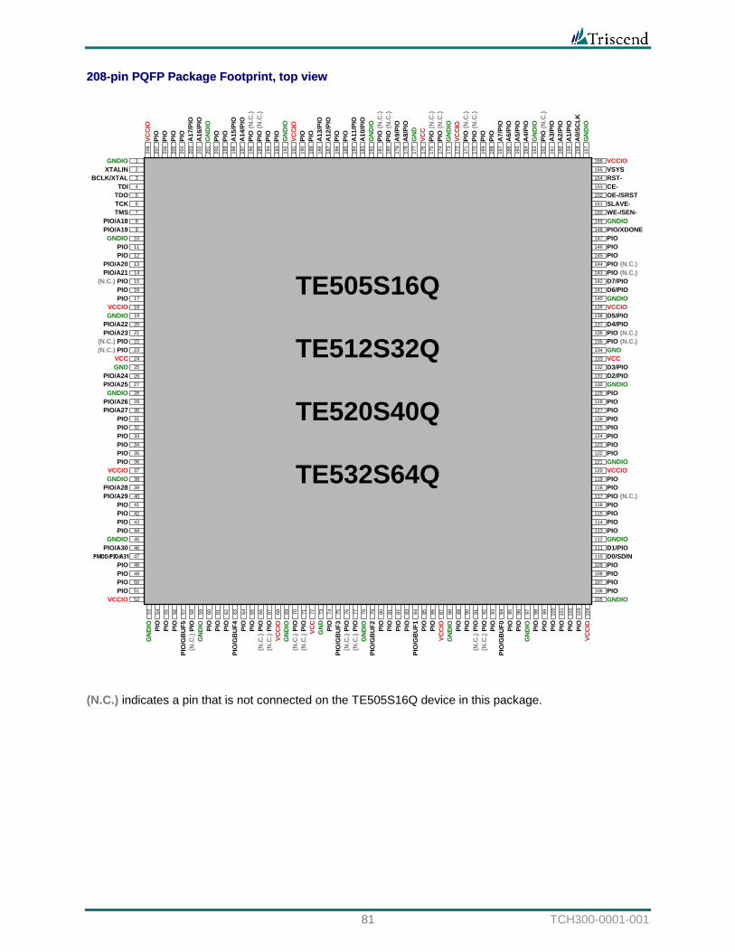
81 TCH300-0001-001
220088--ppiinn PPQQFFPP PPaacckkaaggee FFoooottpprriinntt,, ttoopp vviieeww
208
207
VCC
IO
206
PIO
205
PIO
204
PIO
203
PIO
202
A17
/PIO
201
A16
/PIO
200
GN
DIO
199
PIO
198
PIO
197
A15
/PIO
196
A14
/PIO
195
PIO
(N.C
.)
194
193
PIO
192
PIO
191
GN
DIO
190
VCC
IO
189
PIO
188
PIO
187
A13
/PIO
186
A12
/PIO
185
PIO
184
PIO
183
A11
/PIO
182
GN
DIO
181
A10
/PIO
180
179
178
A9/
PIO
177
A8/
PIO
176
GN
D
175
VCC
174
173
VCC
IO17
2G
ND
IO
171
170
169
PIO
(N.C
.)
168
PIO
167
PIO
166
A7/
PIO
165
A6/
PIO
164
A5/
PIO
163
A4/
PIO
162
GN
DIO
161
PIO
(N.C
.)
160
A3/
PIO
159
A2/
PIO
158
A1/
PIO
157
A0/
SCLK
PIO
(N.C
.)
PIO
(N.C
.)PI
O (N
.C.)
PIO
(N.C
.)PI
O (N
.C.)
PIO
(N.C
.)
GN
DIO
53
PIO
54
PIO
55
PIO
56
PIO
/GB
UF5
57
(N.C
.) PI
O58
GN
DIO
59
PIO
60
PIO
61
PIO
62
PIO
/GB
UF4
63
PIO
64
(N.C
.) PI
O
65
(N.C
.) PI
O66
PIO
67
VCC
IO68
GN
DIO
69 70 71
VCC
72
GN
D73
PIO
74
PIO
/GB
UF3
75
(N.C
.) PI
O76 77
GN
DIO
78
PIO
/GB
UF2
79
PIO
80
PIO
81
PIO
82
PIO
83
PIO
/GB
UF1
84
PIO
85
PIO
86
VCC
IO87
GN
DIO
88
PIO
89
PIO
90 91 92
PIO
93
PIO
/GB
UF0
94
PIO
95
PIO
96
PIO
97
PIO
98G
ND
IO
99
PIO
100
PIO
101
PIO
102
PIO
103
VCC
IO10
4
(N.C
.) PI
O(N
.C.)
PIO
(N.C
.) PI
O
(N.C
.) PI
O(N
.C.)
PIO
GN
DIO
1
2
3
4
5
6
7
8
9
10
11
12
13
14
15
16
17
18
19
20
21
22
23
24
25
26
27
28
29
30
31
32
33
34
35
36
37
38
39
40
41
42
43
44
45
46
47
48
49
50
51
52
156
155VCCIO
154VSYS
153RST-
152CE-
151OE-/SRST
150SLAVE-
149WE-/SEN-
148GNDIO
147PIO/XDONE
146PIO
145
144
PIO (N.C.)143PIO (N.C.)
142
141D7/PIO
140D6/PIO
139GNDIO
138VCCIO
137D5/PIO
136D4/PIO
135
134PIO (N.C.)
133GND
132VCC
131D3/PIO
130D2/PIO
129GNDIO
128
127
126
125
124
D1/PIO
123
D0/SDIN
122PIO
121PIO
120GNDIO
119VCCIO
118
PIO (N.C.)117PIO
116
PIO
115
114
113
GNDIO112
111
110
109
108
107
106
105
PIO (N.C.)
GNDIOPIOPIOPIOPIO
PIOPIOPIOPIO
PIOPIOPIOPIOPIOPIO
PIOPIO
TE505S16Q
TE512S32Q
TE520S40Q
TE532S64Q
XTALINBCLK/XTAL
TDITDOTCKTMS
PIO/A18PIO/A19GNDIO
PIOPIO
(N.C.) PIO
PIO/A20PIO/A21
VCCIOGNDIO
PIO/A22PIO/A23
(N.C.) PIO(N.C.) PIO
VCCGND
PIO/A24PIO/A25GNDIO
PIO/A26PIO/A27
PIO/A28PIO/A29
PIO/A30PMOD/PIO/A31
VCCIOGNDIO
GNDIO
VCCIO
GNDIO
PIO PIO
PIOPIOPIO
PIOPIOPIO
PIOPIOPIOPIO
PIOPIOPIOPIO
(N.C.) indicates a pin that is not connected on the TE505S16Q device in this package.
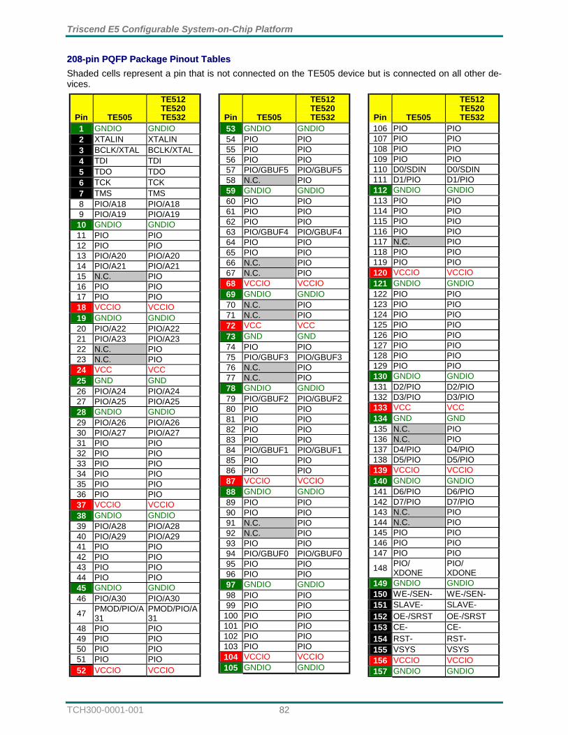
Triscend E5 Configurable System-on-Chip Platform
TCH300-0001-001 82
220088--ppiinn PPQQFFPP PPaacckkaaggee PPiinnoouutt TTaabblleess Shaded cells represent a pin that is not connected on the TE505 device but is connected on all other de-vices.
Pin TE505
TE512 TE520 TE532
1 GNDIO GNDIO 2 XTALIN XTALIN 3 BCLK/XTAL BCLK/XTAL 4 TDI TDI 5 TDO TDO 6 TCK TCK 7 TMS TMS 8 PIO/A18 PIO/A18 9 PIO/A19 PIO/A19
10 GNDIO GNDIO 11 PIO PIO 12 PIO PIO 13 PIO/A20 PIO/A20 14 PIO/A21 PIO/A21 15 N.C. PIO 16 PIO PIO 17 PIO PIO 18 VCCIO VCCIO 19 GNDIO GNDIO 20 PIO/A22 PIO/A22 21 PIO/A23 PIO/A23 22 N.C. PIO 23 N.C. PIO 24 VCC VCC 25 GND GND 26 PIO/A24 PIO/A24 27 PIO/A25 PIO/A25 28 GNDIO GNDIO 29 PIO/A26 PIO/A26 30 PIO/A27 PIO/A27 31 PIO PIO 32 PIO PIO 33 PIO PIO 34 PIO PIO 35 PIO PIO 36 PIO PIO 37 VCCIO VCCIO 38 GNDIO GNDIO 39 PIO/A28 PIO/A28 40 PIO/A29 PIO/A29 41 PIO PIO 42 PIO PIO 43 PIO PIO 44 PIO PIO 45 GNDIO GNDIO 46 PIO/A30 PIO/A30
47 PMOD/PIO/A31
PMOD/PIO/A31
48 PIO PIO 49 PIO PIO 50 PIO PIO 51 PIO PIO 52 VCCIO VCCIO
Pin TE505
TE512 TE520 TE532
53 GNDIO GNDIO 54 PIO PIO 55 PIO PIO 56 PIO PIO 57 PIO/GBUF5 PIO/GBUF5 58 N.C. PIO 59 GNDIO GNDIO 60 PIO PIO 61 PIO PIO 62 PIO PIO 63 PIO/GBUF4 PIO/GBUF4 64 PIO PIO 65 PIO PIO 66 N.C. PIO 67 N.C. PIO 68 VCCIO VCCIO 69 GNDIO GNDIO 70 N.C. PIO 71 N.C. PIO 72 VCC VCC 73 GND GND 74 PIO PIO 75 PIO/GBUF3 PIO/GBUF3 76 N.C. PIO 77 N.C. PIO 78 GNDIO GNDIO 79 PIO/GBUF2 PIO/GBUF2 80 PIO PIO 81 PIO PIO 82 PIO PIO 83 PIO PIO 84 PIO/GBUF1 PIO/GBUF1 85 PIO PIO 86 PIO PIO 87 VCCIO VCCIO 88 GNDIO GNDIO 89 PIO PIO 90 PIO PIO 91 N.C. PIO 92 N.C. PIO 93 PIO PIO 94 PIO/GBUF0 PIO/GBUF0 95 PIO PIO 96 PIO PIO 97 GNDIO GNDIO 98 PIO PIO 99 PIO PIO
100 PIO PIO 101 PIO PIO 102 PIO PIO 103 PIO PIO 104 VCCIO VCCIO 105 GNDIO GNDIO
Pin TE505
TE512 TE520 TE532
106 PIO PIO 107 PIO PIO 108 PIO PIO 109 PIO PIO 110 D0/SDIN D0/SDIN 111 D1/PIO D1/PIO 112 GNDIO GNDIO 113 PIO PIO 114 PIO PIO 115 PIO PIO 116 PIO PIO 117 N.C. PIO 118 PIO PIO 119 PIO PIO 120 VCCIO VCCIO 121 GNDIO GNDIO 122 PIO PIO 123 PIO PIO 124 PIO PIO 125 PIO PIO 126 PIO PIO 127 PIO PIO 128 PIO PIO 129 PIO PIO 130 GNDIO GNDIO 131 D2/PIO D2/PIO 132 D3/PIO D3/PIO 133 VCC VCC 134 GND GND 135 N.C. PIO 136 N.C. PIO 137 D4/PIO D4/PIO 138 D5/PIO D5/PIO 139 VCCIO VCCIO 140 GNDIO GNDIO 141 D6/PIO D6/PIO 142 D7/PIO D7/PIO 143 N.C. PIO 144 N.C. PIO 145 PIO PIO 146 PIO PIO 147 PIO PIO
148 PIO/ XDONE
PIO/ XDONE
149 GNDIO GNDIO 150 WE-/SEN- WE-/SEN- 151 SLAVE- SLAVE- 152 OE-/SRST OE-/SRST 153 CE- CE- 154 RST- RST- 155 VSYS VSYS 156 VCCIO VCCIO 157 GNDIO GNDIO
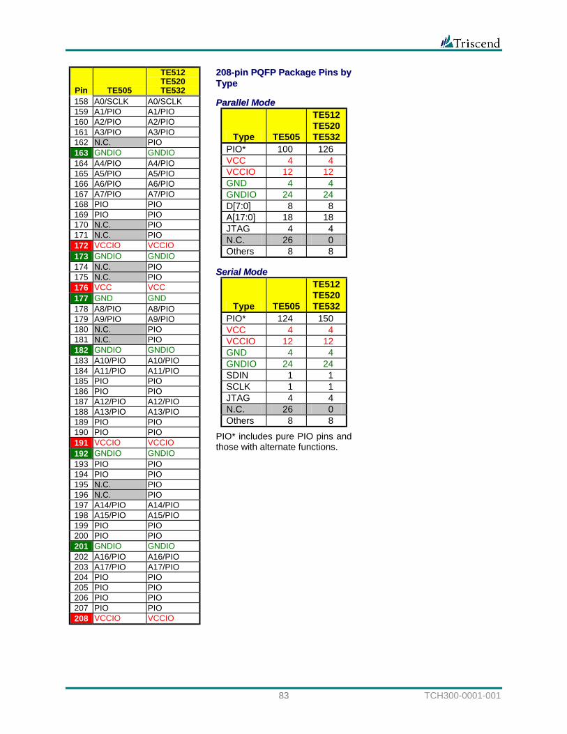
83 TCH300-0001-001
Pin TE505
TE512 TE520 TE532
158 A0/SCLK A0/SCLK 159 A1/PIO A1/PIO 160 A2/PIO A2/PIO 161 A3/PIO A3/PIO 162 N.C. PIO 163 GNDIO GNDIO 164 A4/PIO A4/PIO 165 A5/PIO A5/PIO 166 A6/PIO A6/PIO 167 A7/PIO A7/PIO 168 PIO PIO 169 PIO PIO 170 N.C. PIO 171 N.C. PIO 172 VCCIO VCCIO 173 GNDIO GNDIO 174 N.C. PIO 175 N.C. PIO 176 VCC VCC 177 GND GND 178 A8/PIO A8/PIO 179 A9/PIO A9/PIO 180 N.C. PIO 181 N.C. PIO 182 GNDIO GNDIO 183 A10/PIO A10/PIO 184 A11/PIO A11/PIO 185 PIO PIO 186 PIO PIO 187 A12/PIO A12/PIO 188 A13/PIO A13/PIO 189 PIO PIO 190 PIO PIO 191 VCCIO VCCIO 192 GNDIO GNDIO 193 PIO PIO 194 PIO PIO 195 N.C. PIO 196 N.C. PIO 197 A14/PIO A14/PIO 198 A15/PIO A15/PIO 199 PIO PIO 200 PIO PIO 201 GNDIO GNDIO 202 A16/PIO A16/PIO 203 A17/PIO A17/PIO 204 PIO PIO 205 PIO PIO 206 PIO PIO 207 PIO PIO 208 VCCIO VCCIO
220088--ppiinn PPQQFFPP PPaacckkaaggee PPiinnss bbyy TTyyppee
PPaarraalllleell MMooddee
Type TE505
TE512 TE520 TE532
PIO* 100 126 VCC 4 4 VCCIO 12 12 GND 4 4 GNDIO 24 24 D[7:0] 8 8 A[17:0] 18 18 JTAG 4 4 N.C. 26 0 Others 8 8
SSeerriiaall MMooddee
Type TE505
TE512 TE520 TE532
PIO* 124 150 VCC 4 4 VCCIO 12 12 GND 4 4 GNDIO 24 24 SDIN 1 1 SCLK 1 1 JTAG 4 4 N.C. 26 0 Others 8 8
PIO* includes pure PIO pins and those with alternate functions.
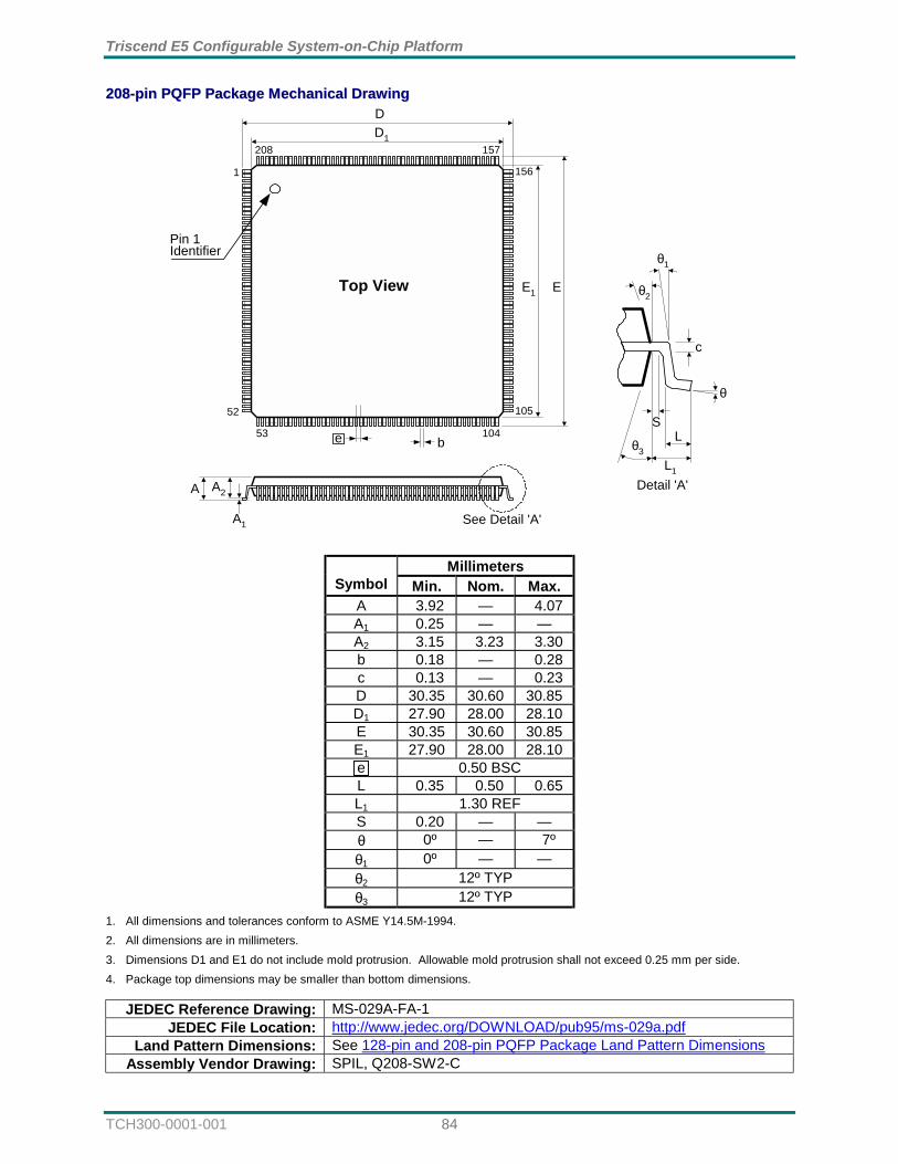
Triscend E5 Configurable System-on-Chip Platform
TCH300-0001-001 84
220088--ppiinn PPQQFFPP PPaacckkaaggee MMeecchhaanniiccaall DDrraawwiinngg
1
52
53 104
105
156
157208
A A2
A1
e b
Pin 1Identifier
See Detail 'A'
D1
D
EE1Top View θ2
θ1
θ3
L1
L
θ
c
Detail 'A'
S
Millimeters Symbol Min. Nom. Max.
A 3.92 — 4.07 A1 0.25 — — A2 3.15 3.23 3.30 b 0.18 — 0.28 c 0.13 — 0.23 D 30.35 30.60 30.85 D1 27.90 28.00 28.10 E 30.35 30.60 30.85 E1 27.90 28.00 28.10 e 0.50 BSC L 0.35 0.50 0.65 L1 1.30 REF S 0.20 — — θ 0º — 7º θ1 0º — — θ2 12º TYP θ3 12º TYP
1. All dimensions and tolerances conform to ASME Y14.5M-1994. 2. All dimensions are in millimeters. 3. Dimensions D1 and E1 do not include mold protrusion. Allowable mold protrusion shall not exceed 0.25 mm per side. 4. Package top dimensions may be smaller than bottom dimensions.
JEDEC Reference Drawing: MS-029A-FA-1 JEDEC File Location: http://www.jedec.org/DOWNLOAD/pub95/ms-029a.pdf
Land Pattern Dimensions: See 128-pin and 208-pin PQFP Package Land Pattern Dimensions Assembly Vendor Drawing: SPIL, Q208-SW2-C
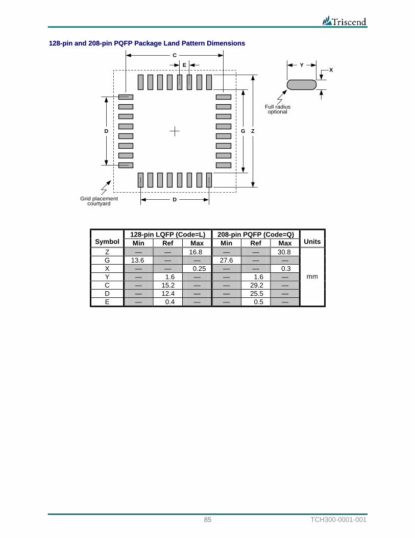
85 TCH300-0001-001
112288--ppiinn aanndd 220088--ppiinn PPQQFFPP PPaacckkaaggee LLaanndd PPaatttteerrnn DDiimmeennssiioonnss C
E
D G Z
D
YX
Full radiusoptional
Grid placementcourtyard
128-pin LQFP (Code=L) 208-pin PQFP (Code=Q) Symbol Min Ref Max Min Ref Max Units
Z — — 16.8 — — 30.8 G 13.6 — — 27.6 — — X — — 0.25 — — 0.3 Y — 1.6 — — 1.6 — C — 15.2 — — 29.2 — D — 12.4 — — 25.5 — E — 0.4 — — 0.5 —
mm
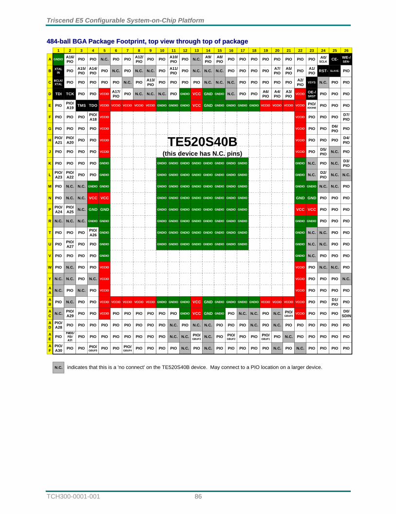
Triscend E5 Configurable System-on-Chip Platform
TCH300-0001-001 86
448844--bbaallll BBGGAA PPaacckkaaggee FFoooottpprriinntt,, ttoopp vviieeww tthhrroouugghh ttoopp ooff ppaacckkaaggee
AB
TDI
PIO
PIO
A17/PIO
A15/PIO
PIO PIO
PIO
PIO
PIO
A11/PIO
PIO
PIO
PIO
PIO
TMS
BCLK/XTAL
1 2 3 4
A
B
C
D
5 6 7 8 9 10 11 12 13 14 15 16 17 18 19 20 21 22 23 24 25 26
PIO
PIOA16/PIO
A14/PIO PIO
PIO
TCK
XTALIN
PIO PIO PIO
PIO
PIO
PIO/A19 TDO
GNDIO
PIO
PIO
PIO
PIO
A12/PIO
A13/PIO PIO
PIO
PIO PIO
A10/PIO
A9/PIO
A8/PIO
PIO
PIO
PIO
PIO
PIO
PIO
PIO
PIO
A7/PIO
PIO
PIO
A6/PIO
A5/PIO
PIO
PIO
A4/PIO
PIO
PIO
PIO
PIO
A1/PIO
A3/PIO
A2/PIO VSYS
OE-/SRST
A0/SCLK
RST-
N.C.
PIO/XDONE
CE-
SLAVE-
PIO
E
F
PIO
PIO
PIO/A18
GNDIO
VCC
GNDIO PIOPIO
WE-/SEN-
G
PIO PIO PIO
PIO
PIO
PIO
PIO
PIO/A20
PIO
PIOPIO
PIO
PIO/A21
PIO
H
PIO PIO PIO
PIO
J
PIO/A23
PIO PIO
PIO
K PIO
PIO/A22L
PIO/A24
M
PIO/A25
N
PIO
PIO
PIO
P
PIO
PIO/A26
PIO/A27
PIO
R
PIO PIO PIO
PIO
T
PIO PIOU
PIO PIOV PIO
PIO
PIOW
Y
PIO/A28
PIOAA
PIO/A29
PIO
PIO
PIO
PMOD/PIO/A31
AC
PIO
PIO/A30
PIO PIO PIO PIO
AD
PIO
PIO PIO PIO PIO PIO PIO PIO PIO PIO
PIO
PIO/GBUF3
PIO/GBUF2
PIO
AE PIO
PIO
PIO PIO PIO PIO PIO PIO PIO
PIO
PIO PIO
AF
PIO
PIO PIO/GBUF5
PIO
PIO PIO
PIO
PIO PIO PIO PIO PIO PIO
PIO
PIO
PIO
PIO/GBUF1
PIO
PIO
PIO
PIO
PIO
PIO
PIO
PIO
PIO/GBUF0
PIO
PIO
PIO
PIO
PIO
PIO PIO
PIO
PIO
PIO
PIO
PIO
D1/PIO
PIO
D0/SDIN
PIO
PIO
PIO
PIO
PIO PIO
PIOPIO
PIO
PIO
PIO
PIO
PIO
PIO
PIO
PIO
PIO
PIO
PIO
PIO
PIO
PIO
PIO
D2/PIO
PIO
D3/PIO
D4/PIO
PIO
PIO
PIO
PIO
D5/PIOPIO
PIO
D6/PIO PIO
PIO
PIO
PIO
D7/PIO
PIO PIO
PIO
PIO
GNDIO GNDIO GNDIO GNDIO
GNDIO GNDIO GNDIO GNDIO
GNDIO GNDIO GNDIO GNDIO
GNDIO GNDIO GNDIO GNDION.C.
TE520S40B(this device has N.C. pins)
indicates that this is a 'no connect' on the TE520S40B device. May connect to a PIO location on a larger device.
N.C.
N.C.
N.C.
N.C.
N.C.
N.C.
N.C.
N.C.
N.C.
N.C.
N.C.
N.C.
N.C.
N.C.
N.C.
N.C.
N.C.
PIO
N.C.
PIO/GBUF4
N.C.
N.C.
N.C.
N.C. N.C.
PIO
PIO
N.C.
N.C. N.C.
N.C.
PIO
N.C.
N.C.
N.C.
N.C.
N.C.
N.C.
N.C.
N.C.
N.C.
N.C. N.C.
N.C.
PIO
PIO
N.C.
N.C.
N.C.
PIO
N.C.
N.C.
N.C.
N.C.
N.C.
N.C.
N.C.
N.C.
N.C.
N.C.
N.C.
N.C.
N.C.
N.C.
N.C.
N.C.
N.C.
N.C.
PIO
PIO
N.C.
N.C.
PIO
PIO
PIO
PIO
N.C.
N.C.
PIO
GNDIO
GNDIO
GNDIO
GNDIO
GNDIO
GNDIO
GNDIO
GNDIO
GNDIOGNDIO GNDIO GNDIO GNDIO GNDIO GNDIO
GNDIO
GNDIO
GNDIO
GNDIO
GNDIO
GNDIO
GNDIO
GNDIO GNDIO GNDIO GNDIO GNDIO GNDIO
GNDIO
GNDIO
GNDIO
GNDIO
GNDIO
GNDIO
GNDIO
GNDIO
GNDIO GNDIO GNDIO GNDIOGNDIO GNDIO
GNDIO GNDIO GNDIO GNDIOGNDIO GNDIO
PIO
VCCIO
VCCIO
VCCIO
VCCIO
VCCIO
VCCIO
GNDIO
GNDIO
GND
GNDIO GNDIO
GNDIO
GNDIO
GNDIO
VCCIO
VCCIO
VCCIO
VCCIO
VCCIO
VCCIO VCCIO VCCIO VCCIO GNDIO GNDIO GNDIO
GNDIO
GNDIO
VCCIO VCCIO VCCIO VCCIO GNDIO GNDIO GNDIO
GNDIO GNDIO
GNDIO GNDIO GNDIO VCCIO
VCCIO
VCCIO VCCIO VCCIO
VCCIO
VCCIO
VCCIO
VCCIO
GNDIO
GNDIO
GNDIO GNDIO
GND
VCC
GNDIOGNDIO
GNDIO
GNDIO
GNDIO
VCCIO
VCCIO
VCCIO
VCCIO
VCCIO
VCCIOVCCIOVCCIOGNDIOGNDIOGNDIOGNDIO
GNDIOGNDVCC
VCC
GND
VCC
VCC
GND
GND
VCC GND
GND
VCC
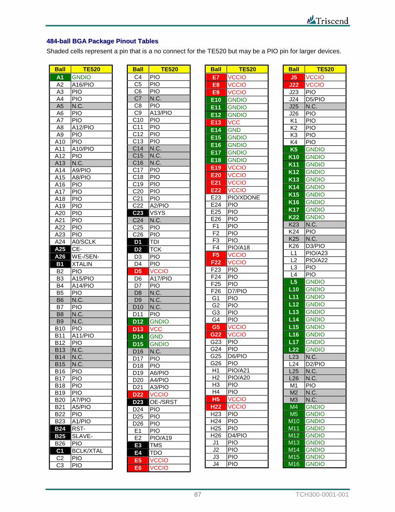
87 TCH300-0001-001
448844--bbaallll BBGGAA PPaacckkaaggee PPiinnoouutt TTaabblleess Shaded cells represent a pin that is a no connect for the TE520 but may be a PIO pin for larger devices.
Ball TE520 A1 GNDIO A2 A16/PIO A3 PIO A4 PIO A5 N.C. A6 PIO A7 PIO A8 A12/PIO A9 PIO
A10 PIO A11 A10/PIO A12 PIO A13 N.C. A14 A9/PIO A15 A8/PIO A16 PIO A17 PIO A18 PIO A19 PIO A20 PIO A21 PIO A22 PIO A23 PIO A24 A0/SCLK A25 CE- A26 WE-/SEN- B1 XTALIN B2 PIO B3 A15/PIO B4 A14/PIO B5 PIO B6 N.C. B7 PIO B8 N.C. B9 N.C.
B10 PIO B11 A11/PIO B12 PIO B13 N.C. B14 N.C. B15 N.C. B16 PIO B17 PIO B18 PIO B19 PIO B20 A7/PIO B21 A5/PIO B22 PIO B23 A1/PIO B24 RST- B25 SLAVE- B26 PIO C1 BCLK/XTAL C2 PIO C3 PIO
Ball TE520 C4 PIO C5 PIO C6 PIO C7 N.C. C8 PIO C9 A13/PIO
C10 PIO C11 PIO C12 PIO C13 PIO C14 N.C. C15 N.C. C16 N.C. C17 PIO C18 PIO C19 PIO C20 PIO C21 PIO C22 A2/PIO C23 VSYS C24 N.C. C25 PIO C26 PIO D1 TDI D2 TCK D3 PIO D4 PIO D5 VCCIO D6 A17/PIO D7 PIO D8 N.C. D9 N.C.
D10 N.C. D11 PIO D12 GNDIO D13 VCC D14 GND D15 GNDIO D16 N.C. D17 PIO D18 PIO D19 A6/PIO D20 A4/PIO D21 A3/PIO D22 VCCIO D23 OE-/SRST D24 PIO D25 PIO D26 PIO E1 PIO E2 PIO/A19 E3 TMS E4 TDO E5 VCCIO E6 VCCIO
Ball TE520 E7 VCCIO E8 VCCIO E9 VCCIO
E10 GNDIO E11 GNDIO E12 GNDIO E13 VCC E14 GND E15 GNDIO E16 GNDIO E17 GNDIO E18 GNDIO E19 VCCIO E20 VCCIO E21 VCCIO E22 VCCIO E23 PIO/XDONE E24 PIO E25 PIO E26 PIO F1 PIO F2 PIO F3 PIO F4 PIO/A18 F5 VCCIO
F22 VCCIO F23 PIO F24 PIO F25 PIO F26 D7/PIO G1 PIO G2 PIO G3 PIO G4 PIO G5 VCCIO
G22 VCCIO G23 PIO G24 PIO G25 D6/PIO G26 PIO H1 PIO/A21 H2 PIO/A20 H3 PIO H4 PIO H5 VCCIO
H22 VCCIO H23 PIO H24 PIO H25 PIO H26 D4/PIO J1 PIO J2 PIO J3 PIO J4 PIO
Ball TE520 J5 VCCIO
J22 VCCIO J23 PIO J24 D5/PIO J25 N.C. J26 PIO K1 PIO K2 PIO K3 PIO K4 PIO K5 GNDIO
K10 GNDIO K11 GNDIO K12 GNDIO K13 GNDIO K14 GNDIO K15 GNDIO K16 GNDIO K17 GNDIO K22 GNDIO K23 N.C. K24 PIO K25 N.C. K26 D3/PIO L1 PIO/A23 L2 PIO/A22 L3 PIO L4 PIO L5 GNDIO
L10 GNDIO L11 GNDIO L12 GNDIO L13 GNDIO L14 GNDIO L15 GNDIO L16 GNDIO L17 GNDIO L22 GNDIO L23 N.C. L24 D2/PIO L25 N.C. L26 N.C. M1 PIO M2 N.C. M3 N.C. M4 GNDIO M5 GNDIO
M10 GNDIO M11 GNDIO M12 GNDIO M13 GNDIO M14 GNDIO M15 GNDIO M16 GNDIO
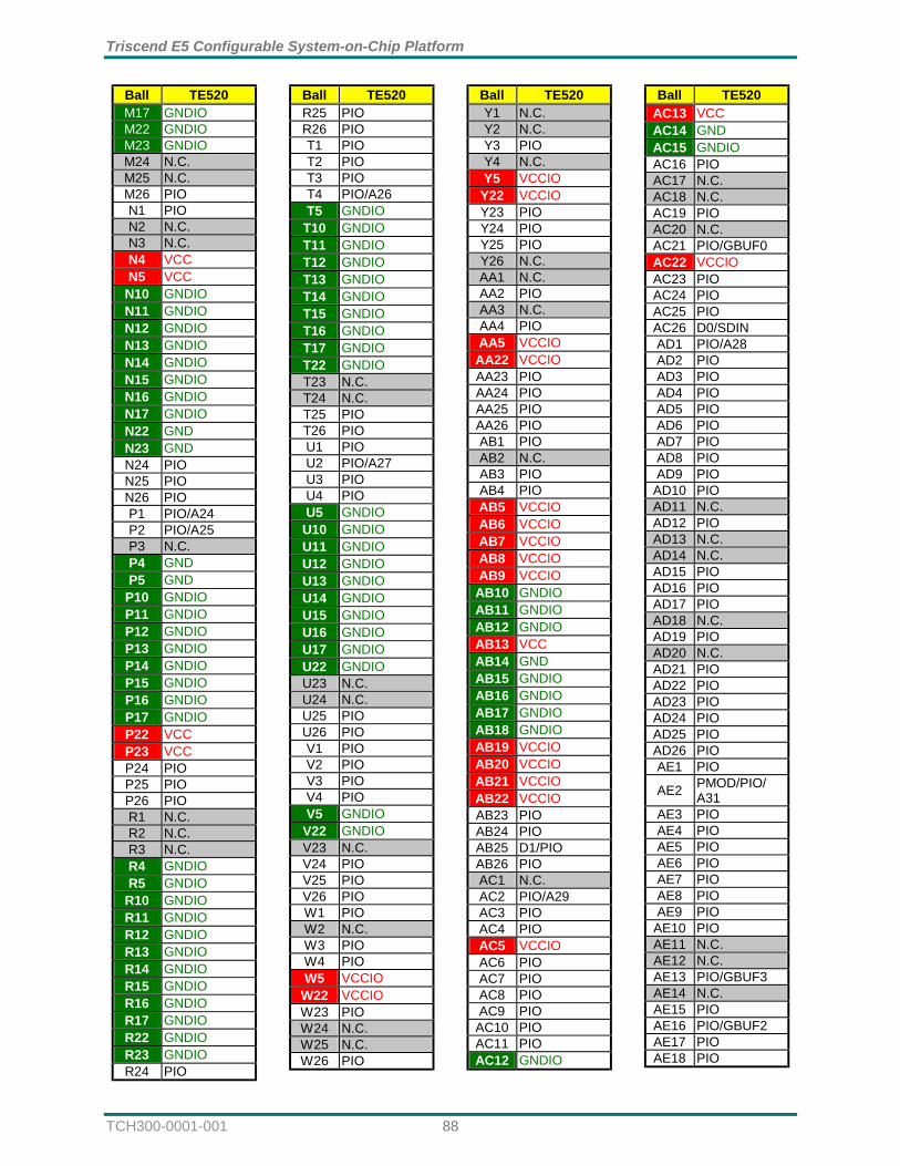
Triscend E5 Configurable System-on-Chip Platform
TCH300-0001-001 88
Ball TE520 M17 GNDIO M22 GNDIO M23 GNDIO M24 N.C. M25 N.C. M26 PIO N1 PIO N2 N.C. N3 N.C. N4 VCC N5 VCC
N10 GNDIO N11 GNDIO N12 GNDIO N13 GNDIO N14 GNDIO N15 GNDIO N16 GNDIO N17 GNDIO N22 GND N23 GND N24 PIO N25 PIO N26 PIO P1 PIO/A24 P2 PIO/A25 P3 N.C. P4 GND P5 GND
P10 GNDIO P11 GNDIO P12 GNDIO P13 GNDIO P14 GNDIO P15 GNDIO P16 GNDIO P17 GNDIO P22 VCC P23 VCC P24 PIO P25 PIO P26 PIO R1 N.C. R2 N.C. R3 N.C. R4 GNDIO R5 GNDIO
R10 GNDIO R11 GNDIO R12 GNDIO R13 GNDIO R14 GNDIO R15 GNDIO R16 GNDIO R17 GNDIO R22 GNDIO R23 GNDIO R24 PIO
Ball TE520 R25 PIO R26 PIO T1 PIO T2 PIO T3 PIO T4 PIO/A26 T5 GNDIO
T10 GNDIO T11 GNDIO T12 GNDIO T13 GNDIO T14 GNDIO T15 GNDIO T16 GNDIO T17 GNDIO T22 GNDIO T23 N.C. T24 N.C. T25 PIO T26 PIO U1 PIO U2 PIO/A27 U3 PIO U4 PIO U5 GNDIO
U10 GNDIO U11 GNDIO U12 GNDIO U13 GNDIO U14 GNDIO U15 GNDIO U16 GNDIO U17 GNDIO U22 GNDIO U23 N.C. U24 N.C. U25 PIO U26 PIO V1 PIO V2 PIO V3 PIO V4 PIO V5 GNDIO
V22 GNDIO V23 N.C. V24 PIO V25 PIO V26 PIO W1 PIO W2 N.C. W3 PIO W4 PIO W5 VCCIO
W22 VCCIO W23 PIO W24 N.C. W25 N.C. W26 PIO
Ball TE520 Y1 N.C. Y2 N.C. Y3 PIO Y4 N.C. Y5 VCCIO
Y22 VCCIO Y23 PIO Y24 PIO Y25 PIO Y26 N.C. AA1 N.C. AA2 PIO AA3 N.C. AA4 PIO AA5 VCCIO
AA22 VCCIO AA23 PIO AA24 PIO AA25 PIO AA26 PIO AB1 PIO AB2 N.C. AB3 PIO AB4 PIO AB5 VCCIO AB6 VCCIO AB7 VCCIO AB8 VCCIO AB9 VCCIO
AB10 GNDIO AB11 GNDIO AB12 GNDIO AB13 VCC AB14 GND AB15 GNDIO AB16 GNDIO AB17 GNDIO AB18 GNDIO AB19 VCCIO AB20 VCCIO AB21 VCCIO AB22 VCCIO AB23 PIO AB24 PIO AB25 D1/PIO AB26 PIO AC1 N.C. AC2 PIO/A29 AC3 PIO AC4 PIO AC5 VCCIO AC6 PIO AC7 PIO AC8 PIO AC9 PIO
AC10 PIO AC11 PIO AC12 GNDIO
Ball TE520 AC13 VCC AC14 GND AC15 GNDIO AC16 PIO AC17 N.C. AC18 N.C. AC19 PIO AC20 N.C. AC21 PIO/GBUF0 AC22 VCCIO AC23 PIO AC24 PIO AC25 PIO AC26 D0/SDIN AD1 PIO/A28 AD2 PIO AD3 PIO AD4 PIO AD5 PIO AD6 PIO AD7 PIO AD8 PIO AD9 PIO
AD10 PIO AD11 N.C. AD12 PIO AD13 N.C. AD14 N.C. AD15 PIO AD16 PIO AD17 PIO AD18 N.C. AD19 PIO AD20 N.C. AD21 PIO AD22 PIO AD23 PIO AD24 PIO AD25 PIO AD26 PIO AE1 PIO
AE2 PMOD/PIO/ A31
AE3 PIO AE4 PIO AE5 PIO AE6 PIO AE7 PIO AE8 PIO AE9 PIO
AE10 PIO AE11 N.C. AE12 N.C. AE13 PIO/GBUF3 AE14 N.C. AE15 PIO AE16 PIO/GBUF2 AE17 PIO AE18 PIO
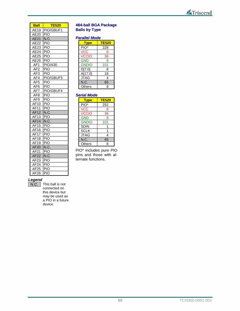
89 TCH300-0001-001
Ball TE520 AE19 PIO/GBUF1 AE20 PIO AE21 N.C. AE22 PIO AE23 PIO AE24 PIO AE25 PIO AE26 PIO AF1 PIO/A30 AF2 PIO AF3 PIO AF4 PIO/GBUF5 AF5 PIO AF6 PIO AF7 PIO/GBUF4 AF8 PIO AF9 PIO
AF10 PIO AF11 PIO AF12 N.C. AF13 PIO AF14 N.C. AF15 PIO AF16 PIO AF17 PIO AF18 PIO AF19 PIO AF20 N.C. AF21 PIO AF22 N.C. AF23 PIO AF24 PIO AF25 PIO AF26 PIO
Legend N.C.
This ball is not connected on this device but may be used as a PIO in a future device.
448844--bbaallll BBGGAA PPaacckkaaggee BBaallllss bbyy TTyyppee
PPaarraalllleell MMooddee Type TE520
PIO* 228 VCC 8 VCCIO 36 GND 8 GNDIO 101 D[7:0] 8 A[17:0] 18 JTAG 4 N.C. 65 Others 8
SSeerriiaall MMooddee Type TE520
PIO* 252 VCC 8 VCCIO 36 GND 8 GNDIO 101 SDIN 1 SCLK 1 JTAG 4 N.C. 65 Others 8
PIO* includes pure PIO pins and those with al-ternate functions.
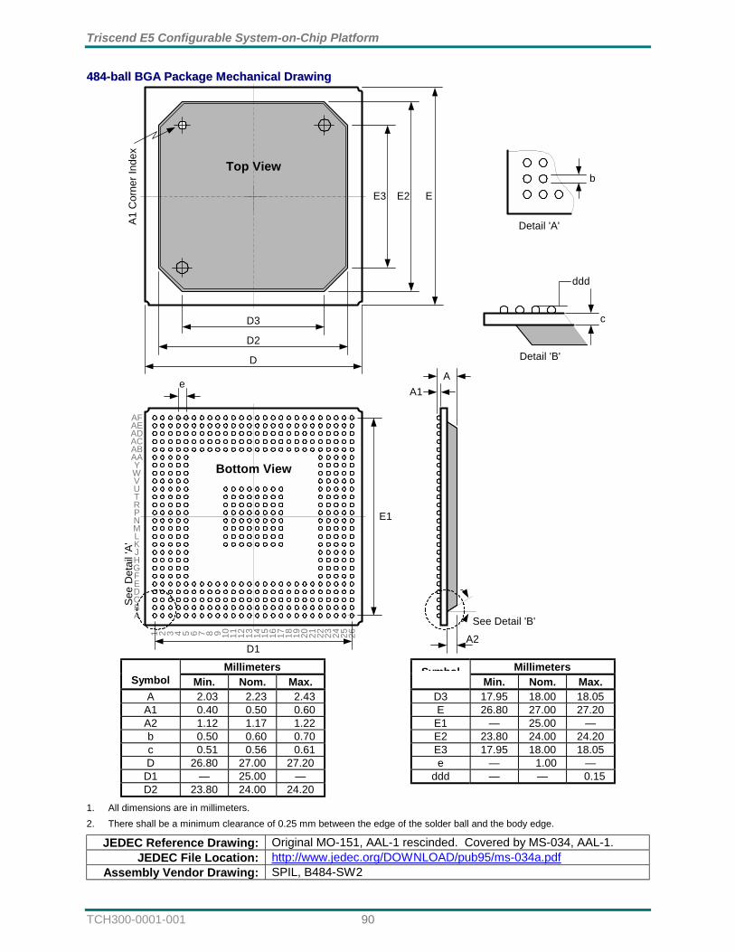
Triscend E5 Configurable System-on-Chip Platform
TCH300-0001-001 90
448844--bbaallll BBGGAA PPaacckkaaggee MMeecchhaanniiccaall DDrraawwiinngg
1 26
BA See Detail 'B'
e
E1
D1A2
A1A
E3 E2 E
D3
D2
D
See
Det
ail '
A'
Detail 'B'
ddd
c
b
Detail 'A'
Top View
Bottom View
CDEFGHJKLMNPRTUVWY
AAABACADAEAF
2 3 4 5 6 7 8 9 10 11 12 13 14 15 16 17 18 19 20 21 22 23 24 25
A1 C
orne
r Ind
ex
Millimeters
Symbol Min. Nom. Max. A 2.03 2.23 2.43
A1 0.40 0.50 0.60 A2 1.12 1.17 1.22 b 0.50 0.60 0.70 c 0.51 0.56 0.61 D 26.80 27.00 27.20
D1 — 25.00 — D2 23.80 24.00 24.20
Millimeters SymbolMin. Nom. Max.
D3 17.95 18.00 18.05 E 26.80 27.00 27.20
E1 — 25.00 — E2 23.80 24.00 24.20 E3 17.95 18.00 18.05 e — 1.00 —
ddd — — 0.15
1. All dimensions are in millimeters. 2. There shall be a minimum clearance of 0.25 mm between the edge of the solder ball and the body edge.
JEDEC Reference Drawing: Original MO-151, AAL-1 rescinded. Covered by MS-034, AAL-1. JEDEC File Location: http://www.jedec.org/DOWNLOAD/pub95/ms-034a.pdf
Assembly Vendor Drawing: SPIL, B484-SW2
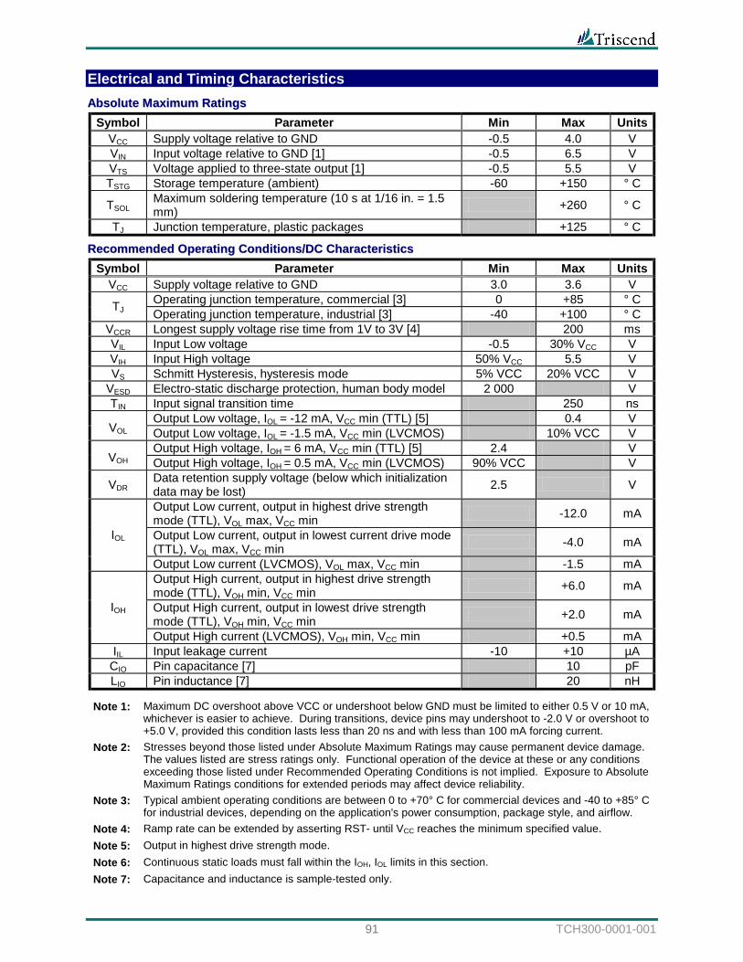
91 TCH300-0001-001
Electrical and Timing Characteristics AAbbssoolluuttee MMaaxxiimmuumm RRaattiinnggss
Symbol Parameter Min Max Units VCC Supply voltage relative to GND -0.5 4.0 V VIN Input voltage relative to GND [1] -0.5 6.5 V VTS Voltage applied to three-state output [1] -0.5 5.5 V TSTG Storage temperature (ambient) -60 +150 ° C
TSOL Maximum soldering temperature (10 s at 1/16 in. = 1.5 mm) +260 ° C
TJ Junction temperature, plastic packages +125 ° C
RReeccoommmmeennddeedd OOppeerraattiinngg CCoonnddiittiioonnss//DDCC CChhaarraacctteerriissttiiccss Symbol Parameter Min Max Units
VCC Supply voltage relative to GND 3.0 3.6 V Operating junction temperature, commercial [3] 0 +85 ° C TJ Operating junction temperature, industrial [3] -40 +100 ° C
VCCR Longest supply voltage rise time from 1V to 3V [4] 200 ms VIL Input Low voltage -0.5 30% VCC V VIH Input High voltage 50% VCC 5.5 V VS Schmitt Hysteresis, hysteresis mode 5% VCC 20% VCC V
VESD Electro-static discharge protection, human body model 2 000 V TIN Input signal transition time 250 ns
Output Low voltage, IOL = -12 mA, VCC min (TTL) [5] 0.4 V VOL Output Low voltage, IOL = -1.5 mA, VCC min (LVCMOS) 10% VCC V
Output High voltage, IOH = 6 mA, VCC min (TTL) [5] 2.4 V VOH Output High voltage, IOH = 0.5 mA, VCC min (LVCMOS) 90% VCC V
VDR Data retention supply voltage (below which initialization data may be lost) 2.5 V
Output Low current, output in highest drive strength mode (TTL), VOL max, VCC min -12.0 mA
Output Low current, output in lowest current drive mode (TTL), VOL max, VCC min -4.0 mA IOL
Output Low current (LVCMOS), VOL max, VCC min -1.5 mA Output High current, output in highest drive strength mode (TTL), VOH min, VCC min +6.0 mA
Output High current, output in lowest drive strength mode (TTL), VOH min, VCC min +2.0 mA IOH
Output High current (LVCMOS), VOH min, VCC min +0.5 mA IIL Input leakage current -10 +10 µA
CIO Pin capacitance [7] 10 pF LIO Pin inductance [7] 20 nH
Note 1: Maximum DC overshoot above VCC or undershoot below GND must be limited to either 0.5 V or 10 mA, whichever is easier to achieve. During transitions, device pins may undershoot to -2.0 V or overshoot to +5.0 V, provided this condition lasts less than 20 ns and with less than 100 mA forcing current.
Note 2: Stresses beyond those listed under Absolute Maximum Ratings may cause permanent device damage. The values listed are stress ratings only. Functional operation of the device at these or any conditions exceeding those listed under Recommended Operating Conditions is not implied. Exposure to Absolute Maximum Ratings conditions for extended periods may affect device reliability.
Note 3: Typical ambient operating conditions are between 0 to +70° C for commercial devices and -40 to +85° C for industrial devices, depending on the application's power consumption, package style, and airflow.
Note 4: Ramp rate can be extended by asserting RST- until VCC reaches the minimum specified value. Note 5: Output in highest drive strength mode. Note 6: Continuous static loads must fall within the IOH, IOL limits in this section. Note 7: Capacitance and inductance is sample-tested only.
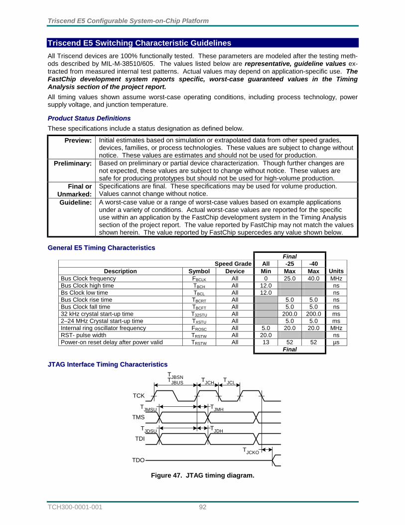
Triscend E5 Configurable System-on-Chip Platform
TCH300-0001-001 92
Triscend E5 Switching Characteristic Guidelines All Triscend devices are 100% functionally tested. These parameters are modeled after the testing meth-ods described by MIL-M-38510/605. The values listed below are representative, guideline values ex-tracted from measured internal test patterns. Actual values may depend on application-specific use. The FastChip development system reports specific, worst-case guaranteed values in the Timing Analysis section of the project report. All timing values shown assume worst-case operating conditions, including process technology, power supply voltage, and junction temperature.
PPrroodduucctt SSttaattuuss DDeeffiinniittiioonnss These specifications include a status designation as defined below.
Preview: Initial estimates based on simulation or extrapolated data from other speed grades, devices, families, or process technologies. These values are subject to change without notice. These values are estimates and should not be used for production.
Preliminary: Based on preliminary or partial device characterization. Though further changes are not expected, these values are subject to change without notice. These values are safe for producing prototypes but should not be used for high-volume production.
Final or Unmarked:
Specifications are final. These specifications may be used for volume production. Values cannot change without notice.
Guideline: A worst-case value or a range of worst-case values based on example applications under a variety of conditions. Actual worst-case values are reported for the specific use within an application by the FastChip development system in the Timing Analysis section of the project report. The value reported by FastChip may not match the values shown herein. The value reported by FastChip supercedes any value shown below.
GGeenneerraall EE55 TTiimmiinngg CChhaarraacctteerriissttiiccss Final
Speed Grade All -25 -40 Description Symbol Device Min Max Max Units
Bus Clock frequency FBCLK All 0 25.0 40.0 MHz Bus Clock high time TBCH All 12.0 ns Bs Clock low time TBCL All 12.0 ns Bus Clock rise time TBCRT All 5.0 5.0 ns Bus Clock fall time TBCFT All 5.0 5.0 ns 32 kHz crystal start-up time T32STU All 200.0 200.0 ms 2–24 MHz Crystal start-up time TXSTU All 5.0 5.0 ms Internal ring oscillator frequency FROSC All 5.0 20.0 20.0 MHz RST- pulse width TRSTW All 20.0 ns Power-on reset delay after power valid TRSTW All 13 52 52 µs
Final
JJTTAAGG IInntteerrffaaccee TTiimmiinngg CChhaarraacctteerriissttiiccss
TCK
TMS
TDI
TDO
TJBUS TJCH TJCL
TJMSU
TJDSU
TJCKO
TJMH
TJDH
TJBSN
Figure 47. JTAG timing diagram.
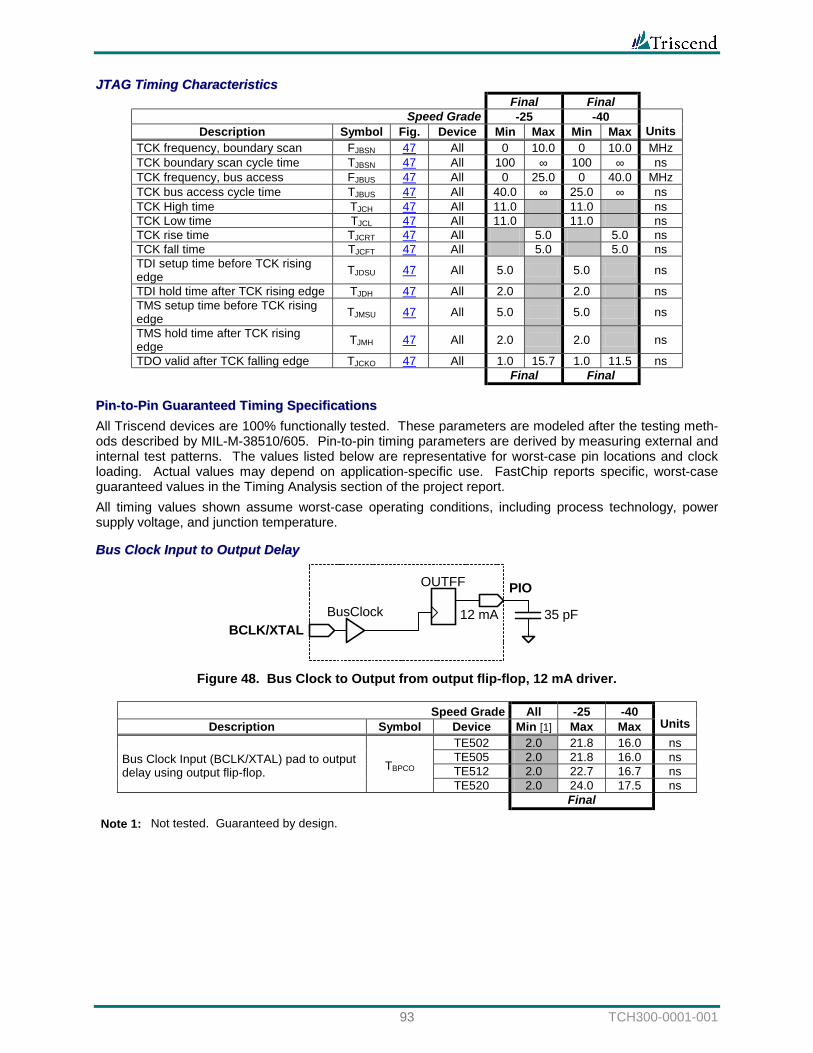
93 TCH300-0001-001
JJTTAAGG TTiimmiinngg CChhaarraacctteerriissttiiccss Final Final
Speed Grade -25 -40 Description Symbol Fig. Device Min Max Min Max Units
TCK frequency, boundary scan FJBSN 47 All 0 10.0 0 10.0 MHz TCK boundary scan cycle time TJBSN 47 All 100 ∞ 100 ∞ ns TCK frequency, bus access FJBUS 47 All 0 25.0 0 40.0 MHz TCK bus access cycle time TJBUS 47 All 40.0 ∞ 25.0 ∞ ns TCK High time TJCH 47 All 11.0 11.0 ns TCK Low time TJCL 47 All 11.0 11.0 ns TCK rise time TJCRT 47 All 5.0 5.0 ns TCK fall time TJCFT 47 All 5.0 5.0 ns TDI setup time before TCK rising edge TJDSU 47 All 5.0 5.0 ns
TDI hold time after TCK rising edge TJDH 47 All 2.0 2.0 ns TMS setup time before TCK rising edge TJMSU 47 All 5.0 5.0 ns
TMS hold time after TCK rising edge TJMH 47 All 2.0 2.0 ns
TDO valid after TCK falling edge TJCKO 47 All 1.0 15.7 1.0 11.5 ns Final Final
PPiinn--ttoo--PPiinn GGuuaarraanntteeeedd TTiimmiinngg SSppeecciiffiiccaattiioonnss All Triscend devices are 100% functionally tested. These parameters are modeled after the testing meth-ods described by MIL-M-38510/605. Pin-to-pin timing parameters are derived by measuring external and internal test patterns. The values listed below are representative for worst-case pin locations and clock loading. Actual values may depend on application-specific use. FastChip reports specific, worst-case guaranteed values in the Timing Analysis section of the project report. All timing values shown assume worst-case operating conditions, including process technology, power supply voltage, and junction temperature.
BBuuss CClloocckk IInnppuutt ttoo OOuuttppuutt DDeellaayy
OUTFF
BusClockBCLK/XTAL
PIO
35 pF12 mA
Figure 48. Bus Clock to Output from output flip-flop, 12 mA driver.
Speed Grade All -25 -40
Description Symbol Device Min [1] Max Max Units TE502 2.0 21.8 16.0 ns TE505 2.0 21.8 16.0 ns TE512 2.0 22.7 16.7 ns
Bus Clock Input (BCLK/XTAL) pad to output delay using output flip-flop. TBPCO
TE520 2.0 24.0 17.5 ns Final
Note 1: Not tested. Guaranteed by design.
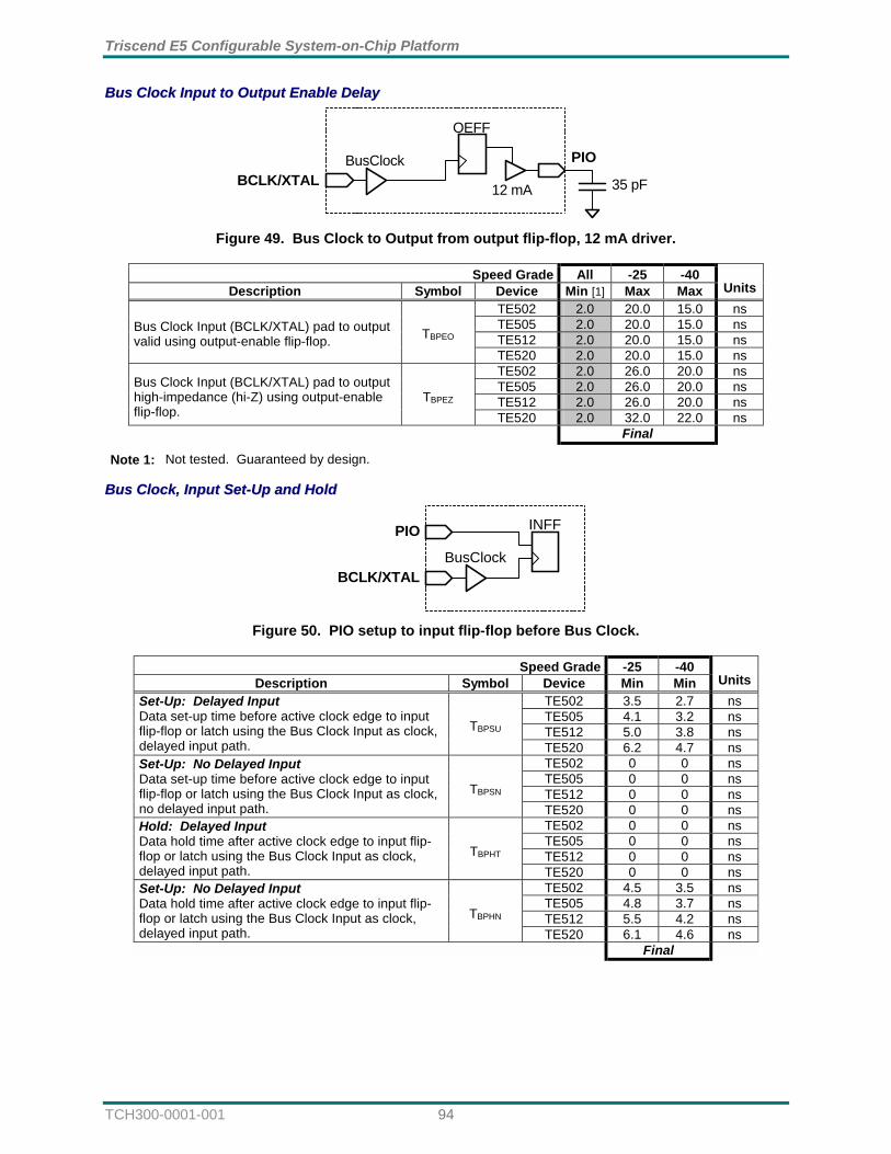
Triscend E5 Configurable System-on-Chip Platform
TCH300-0001-001 94
BBuuss CClloocckk IInnppuutt ttoo OOuuttppuutt EEnnaabbllee DDeellaayy
OEFF
BusClockBCLK/XTAL
PIO
35 pF12 mA
Figure 49. Bus Clock to Output from output flip-flop, 12 mA driver.
Speed Grade All -25 -40
Description Symbol Device Min [1] Max Max Units TE502 2.0 20.0 15.0 ns TE505 2.0 20.0 15.0 ns TE512 2.0 20.0 15.0 ns
Bus Clock Input (BCLK/XTAL) pad to output valid using output-enable flip-flop. TBPEO
TE520 2.0 20.0 15.0 ns TE502 2.0 26.0 20.0 ns TE505 2.0 26.0 20.0 ns TE512 2.0 26.0 20.0 ns
Bus Clock Input (BCLK/XTAL) pad to output high-impedance (hi-Z) using output-enable flip-flop.
TBPEZ TE520 2.0 32.0 22.0 ns
Final
Note 1: Not tested. Guaranteed by design.
BBuuss CClloocckk,, IInnppuutt SSeett--UUpp aanndd HHoolldd
INFF
BusClockBCLK/XTAL
PIO
Figure 50. PIO setup to input flip-flop before Bus Clock.
Speed Grade -25 -40
Description Symbol Device Min Min Units TE502 3.5 2.7 ns TE505 4.1 3.2 ns TE512 5.0 3.8 ns
Set-Up: Delayed Input Data set-up time before active clock edge to input flip-flop or latch using the Bus Clock Input as clock, delayed input path.
TBPSU TE520 6.2 4.7 ns TE502 0 0 ns TE505 0 0 ns TE512 0 0 ns
Set-Up: No Delayed Input Data set-up time before active clock edge to input flip-flop or latch using the Bus Clock Input as clock, no delayed input path.
TBPSN TE520 0 0 ns TE502 0 0 ns TE505 0 0 ns TE512 0 0 ns
Hold: Delayed Input Data hold time after active clock edge to input flip-flop or latch using the Bus Clock Input as clock, delayed input path.
TBPHT TE520 0 0 ns TE502 4.5 3.5 ns TE505 4.8 3.7 ns TE512 5.5 4.2 ns
Set-Up: No Delayed Input Data hold time after active clock edge to input flip-flop or latch using the Bus Clock Input as clock, delayed input path.
TBPHN TE520 6.1 4.6 ns
Final
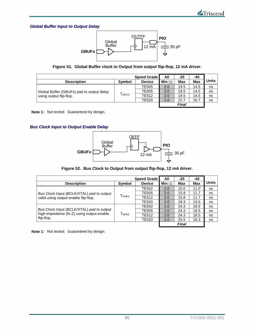
95 TCH300-0001-001
GGlloobbaall BBuuffffeerr IInnppuutt ttoo OOuuttppuutt DDeellaayy
OUTFFGlobalBuffer
GBUFx
PIO
35 pF12 mA
Figure 51. Global Buffer clock to Output from output flip-flop, 12 mA driver.
Speed Grade All -25 -40
Description Symbol Device Min [1] Max Max Units TE505 2.0 19.5 14.5 ns TE505 2.0 19.5 14.5 ns TE512 2.0 19.5 14.5 ns
Global Buffer (GBUFx) pad to output delay using output flip-flop. TGPCO
TE520 2.0 22.7 16.7 ns Final
Note 1: Not tested. Guaranteed by design.
BBuuss CClloocckk IInnppuutt ttoo OOuuttppuutt EEnnaabbllee DDeellaayy
OEFF
GBUFxPIO
35 pF12 mA
GlobalBuffer
Figure 52. Bus Clock to Output from output flip-flop, 12 mA driver.
Speed Grade All -25 -40
Description Symbol Device Min [1] Max Max Units TE502 2.0 15.0 11.0 ns TE505 2.0 15.8 11.7 ns TE512 2.0 15.8 11.7 ns
Bus Clock Input (BCLK/XTAL) pad to output valid using output-enable flip-flop. TGPEO
TE520 2.0 18.3 13.5 ns TE502 2.0 24.3 18.5 ns TE505 2.0 24.3 18.5 ns TE512 2.0 24.3 18.5 ns
Bus Clock Input (BCLK/XTAL) pad to output high-impedance (hi-Z) using output-enable flip-flop.
TGPEZ TE520 2.0 25.5 19.3 ns
Final
Note 1: Not tested. Guaranteed by design.
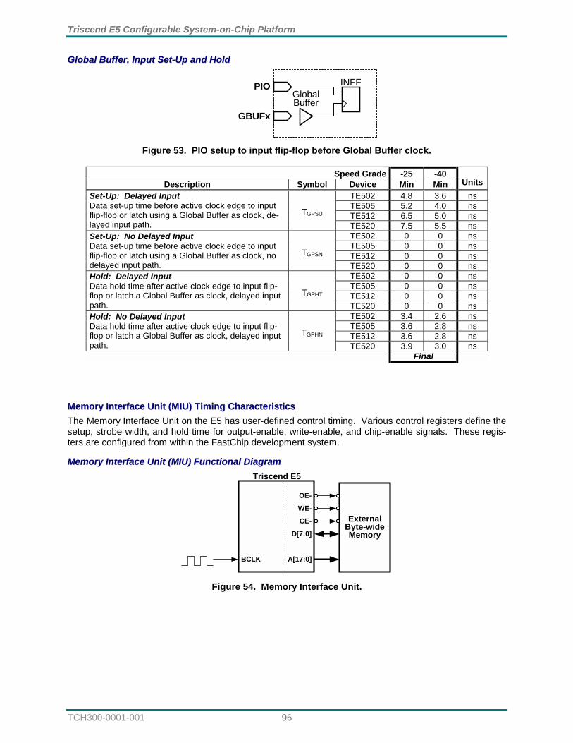
Triscend E5 Configurable System-on-Chip Platform
TCH300-0001-001 96
GGlloobbaall BBuuffffeerr,, IInnppuutt SSeett--UUpp aanndd HHoolldd
INFF
GBUFx
PIOGlobalBuffer
Figure 53. PIO setup to input flip-flop before Global Buffer clock.
Speed Grade -25 -40
Description Symbol Device Min Min Units TE502 4.8 3.6 ns TE505 5.2 4.0 ns TE512 6.5 5.0 ns
Set-Up: Delayed Input Data set-up time before active clock edge to input flip-flop or latch using a Global Buffer as clock, de-layed input path.
TGPSU TE520 7.5 5.5 ns TE502 0 0 ns TE505 0 0 ns TE512 0 0 ns
Set-Up: No Delayed Input Data set-up time before active clock edge to input flip-flop or latch using a Global Buffer as clock, no delayed input path.
TGPSN TE520 0 0 ns TE502 0 0 ns TE505 0 0 ns TE512 0 0 ns
Hold: Delayed Input Data hold time after active clock edge to input flip-flop or latch a Global Buffer as clock, delayed input path.
TGPHT TE520 0 0 ns TE502 3.4 2.6 ns TE505 3.6 2.8 ns TE512 3.6 2.8 ns
Hold: No Delayed Input Data hold time after active clock edge to input flip-flop or latch a Global Buffer as clock, delayed input path.
TGPHN TE520 3.9 3.0 ns
Final
MMeemmoorryy IInntteerrffaaccee UUnniitt ((MMIIUU)) TTiimmiinngg CChhaarraacctteerriissttiiccss The Memory Interface Unit on the E5 has user-defined control timing. Various control registers define the setup, strobe width, and hold time for output-enable, write-enable, and chip-enable signals. These regis-ters are configured from within the FastChip development system.
MMeemmoorryy IInntteerrffaaccee UUnniitt ((MMIIUU)) FFuunnccttiioonnaall DDiiaaggrraamm
A[17:0]
D[7:0]
CE-
WE-
OE-
ExternalByte-wideMemory
Triscend E5
BCLK
Figure 54. Memory Interface Unit.
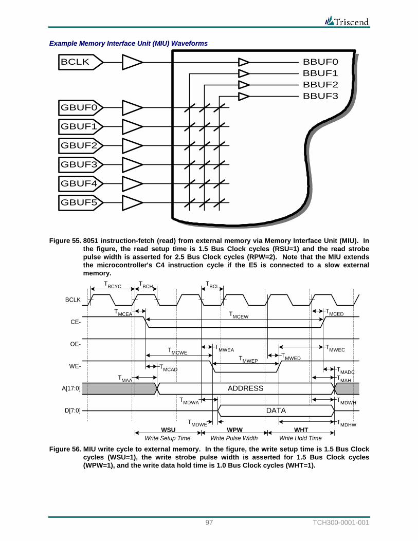
97 TCH300-0001-001
EExxaammppllee MMeemmoorryy IInntteerrffaaccee UUnniitt ((MMIIUU)) WWaavveeffoorrmmss
BBUF0BCLKBBUF1BBUF2BBUF3
GBUF0
GBUF1
GBUF2
GBUF3
GBUF4
GBUF5
Figure 55. 8051 instruction-fetch (read) from external memory via Memory Interface Unit (MIU). In
the figure, the read setup time is 1.5 Bus Clock cycles (RSU=1) and the read strobe pulse width is asserted for 2.5 Bus Clock cycles (RPW=2). Note that the MIU extends the microcontroller's C4 instruction cycle if the E5 is connected to a slow external memory.
BCLK
CE-
OE-
WE-
A[17:0]
D[7:0]
TBCYC TBCH TBCL
TMCEA TMCED
TMWEA
TMDWH
TMAHTMAA
TMCAD
TMCEW
ADDRESS
TMWEDTMWEP
TMCWE
TMDWA
TMDWE TMDHW
TMADC
DATA
TMWEC
WSUWrite Setup Time
WPWWrite Pulse Width
WHTWrite Hold Time
Figure 56. MIU write cycle to external memory. In the figure, the write setup time is 1.5 Bus Clock cycles (WSU=1), the write strobe pulse width is asserted for 1.5 Bus Clock cycles (WPW=1), and the write data hold time is 1.0 Bus Clock cycles (WHT=1).
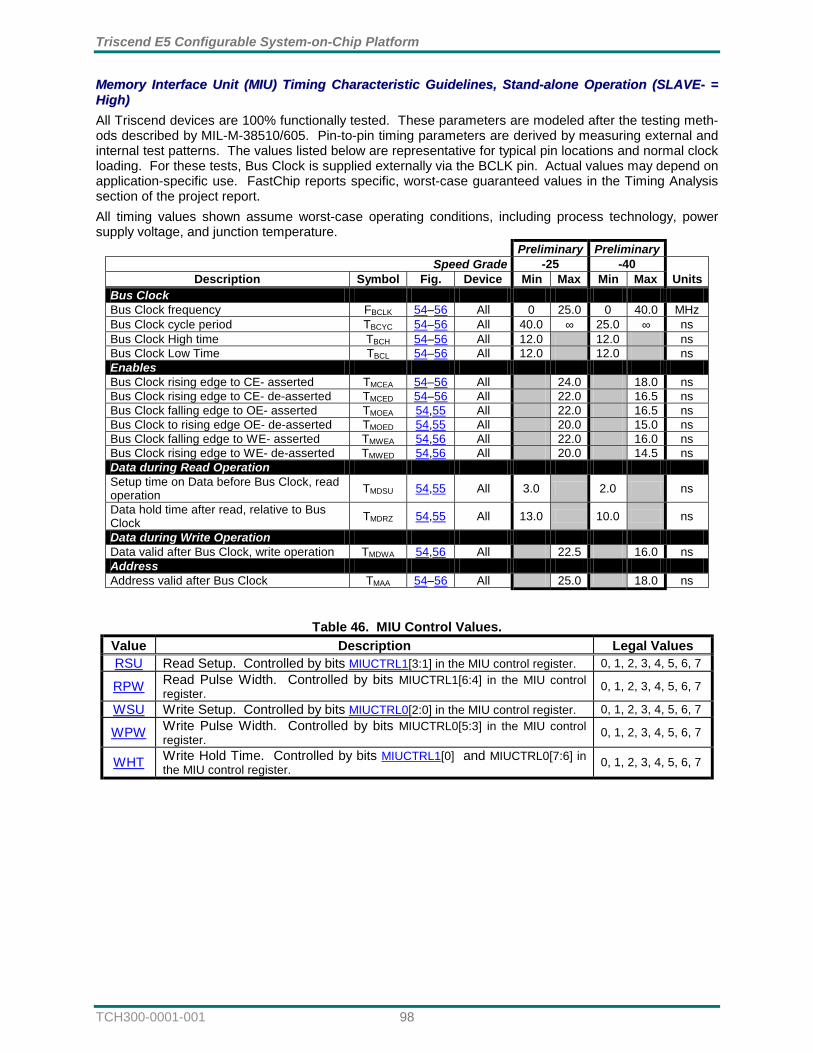
Triscend E5 Configurable System-on-Chip Platform
TCH300-0001-001 98
MMeemmoorryy IInntteerrffaaccee UUnniitt ((MMIIUU)) TTiimmiinngg CChhaarraacctteerriissttiicc GGuuiiddeelliinneess,, SSttaanndd--aalloonnee OOppeerraattiioonn ((SSLLAAVVEE-- == HHiigghh)) All Triscend devices are 100% functionally tested. These parameters are modeled after the testing meth-ods described by MIL-M-38510/605. Pin-to-pin timing parameters are derived by measuring external and internal test patterns. The values listed below are representative for typical pin locations and normal clock loading. For these tests, Bus Clock is supplied externally via the BCLK pin. Actual values may depend on application-specific use. FastChip reports specific, worst-case guaranteed values in the Timing Analysis section of the project report. All timing values shown assume worst-case operating conditions, including process technology, power supply voltage, and junction temperature.
Preliminary Preliminary Speed Grade -25 -40
Description Symbol Fig. Device Min Max Min Max Units Bus Clock Bus Clock frequency FBCLK 54–56 All 0 25.0 0 40.0 MHz Bus Clock cycle period TBCYC 54–56 All 40.0 ∞ 25.0 ∞ ns Bus Clock High time TBCH 54–56 All 12.0 12.0 ns Bus Clock Low Time TBCL 54–56 All 12.0 12.0 ns Enables Bus Clock rising edge to CE- asserted TMCEA 54–56 All 24.0 18.0 ns Bus Clock rising edge to CE- de-asserted TMCED 54–56 All 22.0 16.5 ns Bus Clock falling edge to OE- asserted TMOEA 54,55 All 22.0 16.5 ns Bus Clock to rising edge OE- de-asserted TMOED 54,55 All 20.0 15.0 ns Bus Clock falling edge to WE- asserted TMWEA 54,56 All 22.0 16.0 ns Bus Clock rising edge to WE- de-asserted TMWED 54,56 All 20.0 14.5 ns Data during Read Operation Setup time on Data before Bus Clock, read operation TMDSU 54,55 All 3.0 2.0 ns
Data hold time after read, relative to Bus Clock TMDRZ 54,55 All 13.0 10.0 ns
Data during Write Operation Data valid after Bus Clock, write operation TMDWA 54,56 All 22.5 16.0 ns Address Address valid after Bus Clock TMAA 54–56 All 25.0 18.0 ns
Table 46. MIU Control Values. Value Description Legal Values RSU Read Setup. Controlled by bits MIUCTRL1[3:1] in the MIU control register. 0, 1, 2, 3, 4, 5, 6, 7
RPW Read Pulse Width. Controlled by bits MIUCTRL1[6:4] in the MIU control register. 0, 1, 2, 3, 4, 5, 6, 7
WSU Write Setup. Controlled by bits MIUCTRL0[2:0] in the MIU control register. 0, 1, 2, 3, 4, 5, 6, 7
WPW Write Pulse Width. Controlled by bits MIUCTRL0[5:3] in the MIU control register. 0, 1, 2, 3, 4, 5, 6, 7
WHT Write Hold Time. Controlled by bits MIUCTRL1[0] and MIUCTRL0[7:6] in the MIU control register. 0, 1, 2, 3, 4, 5, 6, 7
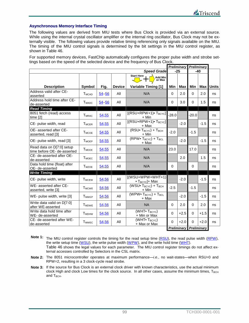
99 TCH300-0001-001
AAssyynncchhrroonnoouuss MMeemmoorryy IInntteerrffaaccee TTiimmiinngg The following values are derived from MIU tests where Bus Clock is provided via an external source. While using the internal crystal oscillator amplifier or the internal ring oscillator, Bus Clock may not be ex-ternally visible. The following values provide relative timing referencing only signals available on the MIU. The timing of the MIU control signals is determined by the bit settings in the MIU control register, as shown in Table 46. For supported memory devices, FastChip automatically configures the proper pulse width and strobe set-tings based on the speed of the selected device and the frequency of Bus Clock. Preliminary Preliminary Speed Grade -25 -40
Description Symbol Fig. Device
Start Here Add Minor Max
Variable Timing [1] Min Max Min Max Units Address valid after CE- asserted TMCAD 54–56 All N/A 0 2.0 0 2.0 ns
Address hold time after CE- de-asserted TMADC 54–56 All N/A 0 3.0 0 1.5 ns
Read Timing 8051 fetch (read) access time [2] TMRAC 54,55 All [(RSU+RPW+1)• TBCYC]
+ Min -28.0 -20.0 ns
CE- pulse width, read TMCER 54,55 All [(RSU+RPW+1)• TBCYC] + Max -2.0 -1.5 ns
OE- asserted after CE- asserted, read [3] TMCOE 54,55 All (RSU• TBCYC) + TBCH
+ Min -2.0 -1.5 ns
OE- pulse width, read [3] TMOEP 54,55 All (RPW• TBCYC) + TBCL + Max -2.0 -1.5 ns
Read data on D[7:0] setup time before OE- de-asserted TMDOE 54,55 All N/A 23.0 17.0 ns
CE- de-asserted after OE- de-asserted TMOEC 54,55 All N/A 2.0 1.5 ns
Data hold time (float) after OE- de-asserted TMZOE 54,55 All N/A 0 0 ns
Write Timing
CE- pulse width, write TMCEW 54,56 All [(WSU+WPW+WHT+1)• TBCYC]+ Max -2.0 -1.5 ns
WE- asserted after CE- asserted, write [3] TMCWE 54,56 All (WSU• TBCYC) + TBCH
+ Min -2.5 -1.5 ns
WE- pulse width, write [3] TMWEP 54,56 All (WPW• TBCYC) + TBCL + Max -2.0 -1.5 ns
Write data valid on D[7:0] after WE-asserted TMDWE 54,56 All NA 0 2.0 0 2.0 ns
Write data hold time after WE- de-asserted TMDHW 54,56 All (WHT• TBCYC)
+ Min or Max 0 +2.5 0 +1.5 ns
CE- de-asserted after WE- de-asserted TMWEC 54,56 All (WHT• TBCYC)
+ Max or Max 0 +2.0 0 +2.0 ns Preliminary Preliminary
Note 1: The MIU control register controls the timing for the read setup time (RSU), the read pulse width (RPW), the write setup time (WSU), the write pulse width (WPW), and the write hold time (WHT). Table 46 shows the legal values for each parameter. The MIU control register timings do not affect ex-ternal accesses controlled by Selectors in the CSL matrix.
Note 2: The 8051 microcontroller operates at maximum performance—i.e., no wait-states—when RSU=0 and RPW=2, resulting in a 3 clock-cycle read strobe.
Note 3: If the source for Bus Clock is an external clock driver with known characteristics, use the actual minimum clock High and clock Low times for the clock source. In all other cases, assume the minimum times, TBCH and TBCH.
Triscend E5 Configurable System-on-Chip Platform
TCH300-0001-001 100
CCoonnffiigguurraabbllee SSyysstteemm IInntteerrccoonnnneecctt ((CCSSII)) SSoocckkeett TTiimmiinngg GGuuiiddeelliinneess The Triscend Configurable System Interconnect (CSI) bus socket provides a family-independent interface between the processor, its peripherals, and the Configurable System Logic (CSL) matrix. The following values provide a typical range of worst-case delays based on test designs. The actual values depend on a variety of factors including how the CSL logic cells connect to the CSI bus in the application, the utiliza-tion of the CSL matrix, and the number of modules in the design. The tables also show how much addi-tional logic delay, or slack time, is allowed in each type of logic path while operating at the maximum bus clock frequency, FBCLK.
CCSSII SSoocckkeett FFuunnccttiioonnaall DDiiaaggrraamm
32Address
Data Write8
DMA ReqSel
WaitNext
Break
Selector RdSel
Selector WrSel
ChipSel RdSel
ChipSel Sel
DMA AckSel
Waited
Event
Bus Clock
Data
Address
Selector
ChipSel
DMACtrlWaitCtrlBrkPntBusClk
8Data Read
Enable
Figure 57. Configurable System Interconnect (CSI) bus socket.
CCSSII SSoocckkeett TTiimmiinngg BBeenncchhmmaarrkk CCiirrccuuiittss
D
EN
Data Write
WrSel, Sel, AckSel
Bus Clock
Q
CSI BusSocket
8
Byte-WideData Register
Figure 58. CSI bus write to byte-wide register.
4
DI
WE
Data Write
WrSel, Sel, AckSel
Bus Clock
O
CSI BusSocket
8
16x8 RAM
AAddress
Figure 59. CSI bus write to 16x8 RAM.
8D
ENRdSel, Sel, AckSel
Q
CSI BusSocket
Byte-WideData Register
Data Read
Enable
Figure 60. CSI bus read from byte-wide register.
4
8Data ReadDI
WE
O
16x8 RAM
AAddress
EnableRdSel, Sel, AckSel
CSI BusSocket
Figure 61. CSI bus read from 16x8 RAM.
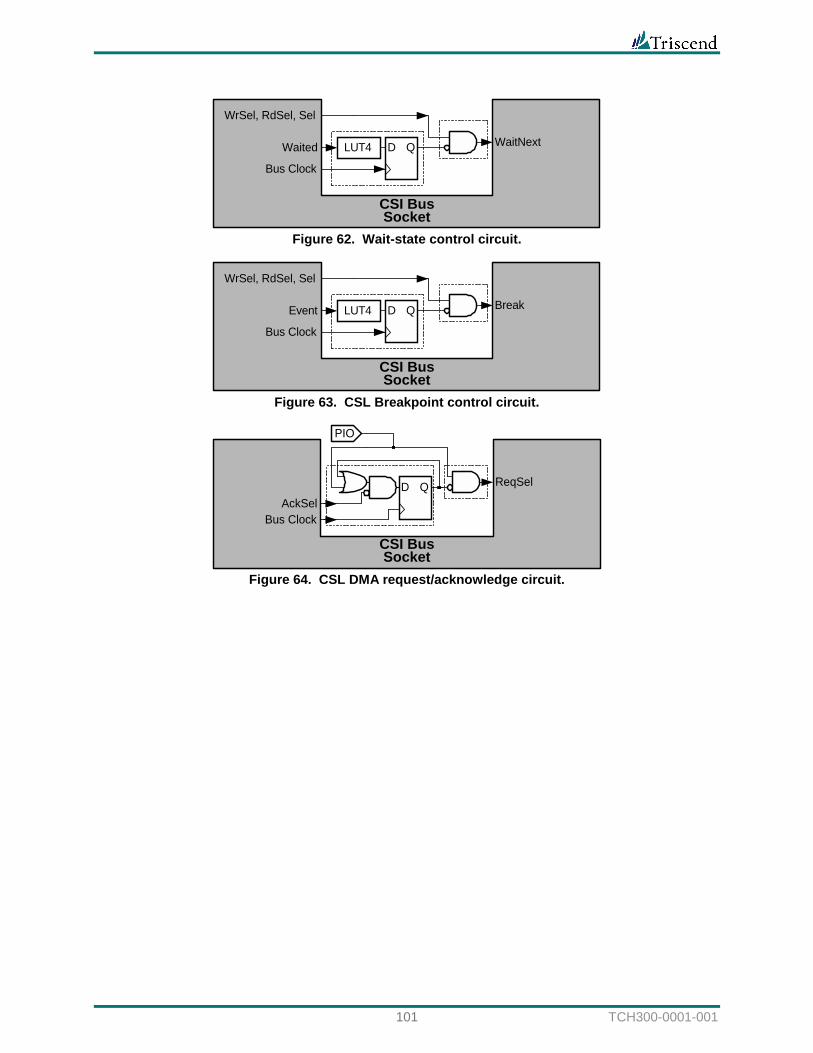
101 TCH300-0001-001
CSI BusSocket
D QLUT4
WrSel, RdSel, Sel
Waited
Bus Clock
WaitNext
Figure 62. Wait-state control circuit.
CSI BusSocket
D QLUT4
WrSel, RdSel, Sel
Event
Bus Clock
Break
Figure 63. CSL Breakpoint control circuit.
CSI BusSocket
AckSel
ReqSel
Bus Clock
PIO
D Q
Figure 64. CSL DMA request/acknowledge circuit.
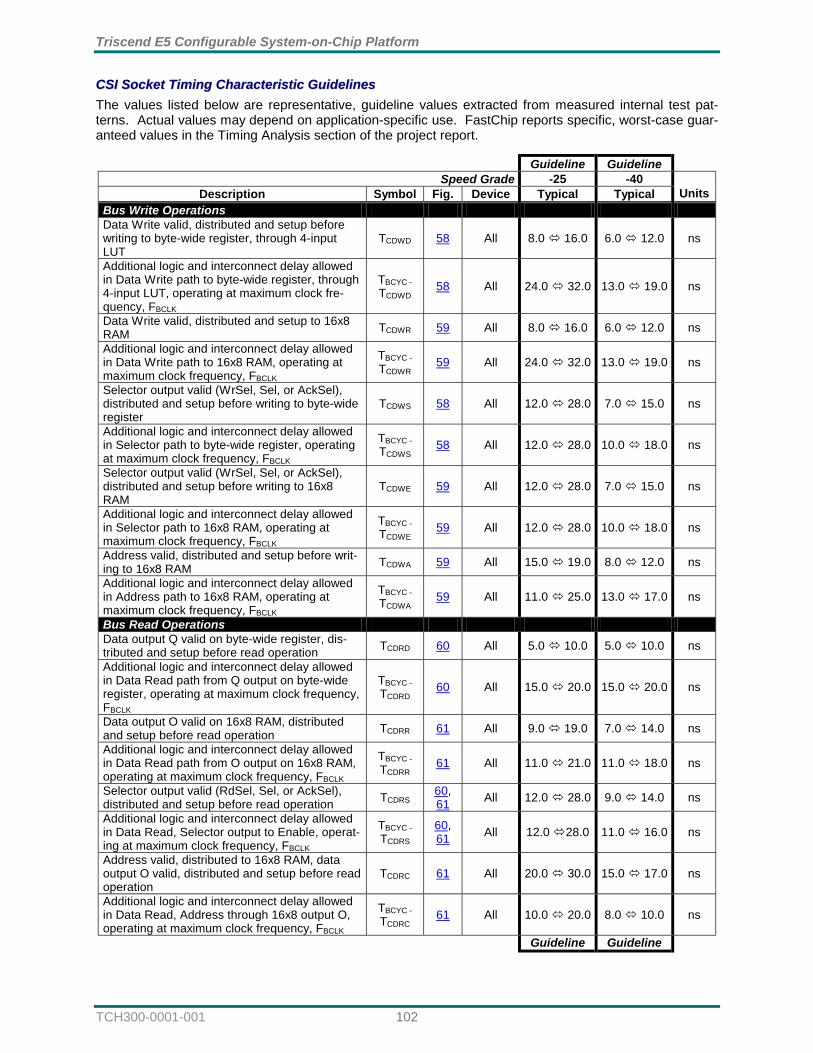
Triscend E5 Configurable System-on-Chip Platform
TCH300-0001-001 102
CCSSII SSoocckkeett TTiimmiinngg CChhaarraacctteerriissttiicc GGuuiiddeelliinneess The values listed below are representative, guideline values extracted from measured internal test pat-terns. Actual values may depend on application-specific use. FastChip reports specific, worst-case guar-anteed values in the Timing Analysis section of the project report.
Guideline Guideline Speed Grade -25 -40
Description Symbol Fig. Device Typical Typical Units Bus Write Operations Data Write valid, distributed and setup before writing to byte-wide register, through 4-input LUT
TCDWD 58 All 8.0 ) 16.0 6.0 ) 12.0 ns
Additional logic and interconnect delay allowed in Data Write path to byte-wide register, through 4-input LUT, operating at maximum clock fre-quency, FBCLK
TBCYC - TCDWD 58 All 24.0 ) 32.0 13.0 ) 19.0 ns
Data Write valid, distributed and setup to 16x8 RAM TCDWR 59 All 8.0 ) 16.0 6.0 ) 12.0 ns
Additional logic and interconnect delay allowed in Data Write path to 16x8 RAM, operating at maximum clock frequency, FBCLK
TBCYC - TCDWR 59 All 24.0 ) 32.0 13.0 ) 19.0 ns
Selector output valid (WrSel, Sel, or AckSel), distributed and setup before writing to byte-wide register
TCDWS 58 All 12.0 ) 28.0 7.0 ) 15.0 ns
Additional logic and interconnect delay allowed in Selector path to byte-wide register, operating at maximum clock frequency, FBCLK
TBCYC - TCDWS 58 All 12.0 ) 28.0 10.0 ) 18.0 ns
Selector output valid (WrSel, Sel, or AckSel), distributed and setup before writing to 16x8 RAM
TCDWE 59 All 12.0 ) 28.0 7.0 ) 15.0 ns
Additional logic and interconnect delay allowed in Selector path to 16x8 RAM, operating at maximum clock frequency, FBCLK
TBCYC - TCDWE 59 All 12.0 ) 28.0 10.0 ) 18.0 ns
Address valid, distributed and setup before writ-ing to 16x8 RAM TCDWA 59 All 15.0 ) 19.0 8.0 ) 12.0 ns
Additional logic and interconnect delay allowed in Address path to 16x8 RAM, operating at maximum clock frequency, FBCLK
TBCYC - TCDWA 59 All 11.0 ) 25.0 13.0 ) 17.0 ns
Bus Read Operations Data output Q valid on byte-wide register, dis-tributed and setup before read operation TCDRD 60 All 5.0 ) 10.0 5.0 ) 10.0 ns
Additional logic and interconnect delay allowed in Data Read path from Q output on byte-wide register, operating at maximum clock frequency, FBCLK
TBCYC - TCDRD 60 All 15.0 ) 20.0 15.0 ) 20.0 ns
Data output O valid on 16x8 RAM, distributed and setup before read operation TCDRR 61 All 9.0 ) 19.0 7.0 ) 14.0 ns
Additional logic and interconnect delay allowed in Data Read path from O output on 16x8 RAM, operating at maximum clock frequency, FBCLK
TBCYC - TCDRR 61 All 11.0 ) 21.0 11.0 ) 18.0 ns
Selector output valid (RdSel, Sel, or AckSel), distributed and setup before read operation TCDRS 60,
61 All 12.0 ) 28.0 9.0 ) 14.0 ns
Additional logic and interconnect delay allowed in Data Read, Selector output to Enable, operat-ing at maximum clock frequency, FBCLK
TBCYC - TCDRS
60, 61 All 12.0 )28.0 11.0 ) 16.0 ns
Address valid, distributed to 16x8 RAM, data output O valid, distributed and setup before read operation
TCDRC 61 All 20.0 ) 30.0 15.0 ) 17.0 ns
Additional logic and interconnect delay allowed in Data Read, Address through 16x8 output O, operating at maximum clock frequency, FBCLK
TBCYC - TCDRC 61 All 10.0 ) 20.0 8.0 ) 10.0 ns
Guideline Guideline
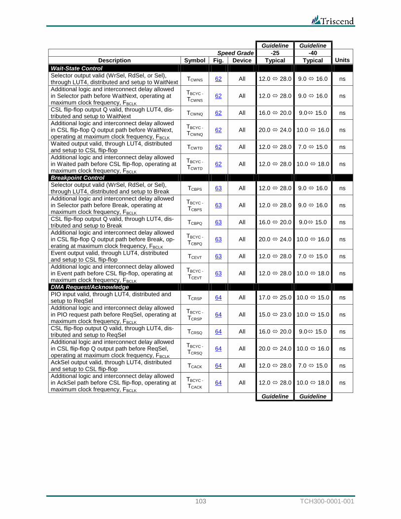
103 TCH300-0001-001
Guideline Guideline Speed Grade -25 -40
Description Symbol Fig. Device Typical Typical Units Wait-State Control Selector output valid (WrSel, RdSel, or Sel), through LUT4, distributed and setup to WaitNext TCWNS 62 All 12.0 ) 28.0 9.0 ) 16.0 ns
Additional logic and interconnect delay allowed in Selector path before WaitNext, operating at maximum clock frequency, FBCLK
TBCYC - TCWNS 62 All 12.0 ) 28.0 9.0 ) 16.0 ns
CSL flip-flop output Q valid, through LUT4, dis-tributed and setup to WaitNext TCWNQ 62 All 16.0 ) 20.0 9.0) 15.0 ns
Additional logic and interconnect delay allowed in CSL flip-flop Q output path before WaitNext, operating at maximum clock frequency, FBCLK
TBCYC - TCWNQ 62 All 20.0 ) 24.0 10.0 ) 16.0 ns
Waited output valid, through LUT4, distributed and setup to CSL flip-flop TCWTD 62 All 12.0 ) 28.0 7.0 ) 15.0 ns
Additional logic and interconnect delay allowed in Waited path before CSL flip-flop, operating at maximum clock frequency, FBCLK
TBCYC - TCWTD 62 All 12.0 ) 28.0 10.0 ) 18.0 ns
Breakpoint Control Selector output valid (WrSel, RdSel, or Sel), through LUT4, distributed and setup to Break TCBPS 63 All 12.0 ) 28.0 9.0 ) 16.0 ns
Additional logic and interconnect delay allowed in Selector path before Break, operating at maximum clock frequency, FBCLK
TBCYC - TCBPS 63 All 12.0 ) 28.0 9.0 ) 16.0 ns
CSL flip-flop output Q valid, through LUT4, dis-tributed and setup to Break TCBPQ 63 All 16.0 ) 20.0 9.0) 15.0 ns
Additional logic and interconnect delay allowed in CSL flip-flop Q output path before Break, op-erating at maximum clock frequency, FBCLK
TBCYC - TCBPQ 63 All 20.0 ) 24.0 10.0 ) 16.0 ns
Event output valid, through LUT4, distributed and setup to CSL flip-flop TCEVT 63 All 12.0 ) 28.0 7.0 ) 15.0 ns
Additional logic and interconnect delay allowed in Event path before CSL flip-flop, operating at maximum clock frequency, FBCLK
TBCYC - TCEVT 63 All 12.0 ) 28.0 10.0 ) 18.0 ns
DMA Request/Acknowledge PIO input valid, through LUT4, distributed and setup to ReqSel TCRSP 64 All 17.0 ) 25.0 10.0 ) 15.0 ns
Additional logic and interconnect delay allowed in PIO request path before ReqSel, operating at maximum clock frequency, FBCLK
TBCYC - TCRSP 64 All 15.0 ) 23.0 10.0 ) 15.0 ns
CSL flip-flop output Q valid, through LUT4, dis-tributed and setup to ReqSel TCRSQ 64 All 16.0 ) 20.0 9.0) 15.0 ns
Additional logic and interconnect delay allowed in CSL flip-flop Q output path before ReqSel, operating at maximum clock frequency, FBCLK
TBCYC - TCRSQ 64 All 20.0 ) 24.0 10.0 ) 16.0 ns
AckSel output valid, through LUT4, distributed and setup to CSL flip-flop TCACK 64 All 12.0 ) 28.0 7.0 ) 15.0 ns
Additional logic and interconnect delay allowed in AckSel path before CSL flip-flop, operating at maximum clock frequency, FBCLK
TBCYC - TCACK 64 All 12.0 ) 28.0 10.0 ) 18.0 ns
Guideline Guideline
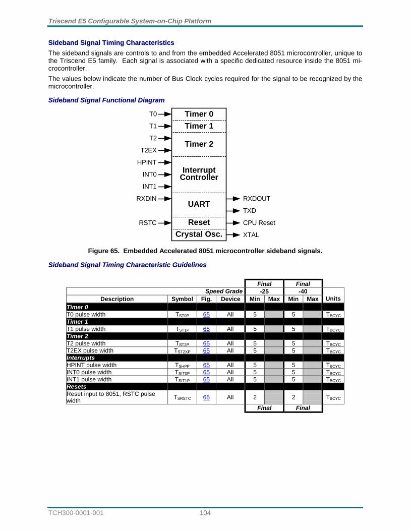
Triscend E5 Configurable System-on-Chip Platform
TCH300-0001-001 104
SSiiddeebbaanndd SSiiggnnaall TTiimmiinngg CChhaarraacctteerriissttiiccss The sideband signals are controls to and from the embedded Accelerated 8051 microcontroller, unique to the Triscend E5 family. Each signal is associated with a specific dedicated resource inside the 8051 mi-crocontroller. The values below indicate the number of Bus Clock cycles required for the signal to be recognized by the microcontroller.
SSiiddeebbaanndd SSiiggnnaall FFuunnccttiioonnaall DDiiaaggrraamm
XTAL
Timer 0
RXDOUT
TXD
RXDIN
INT1
INT0
HPINT
T0
T1
T2
T2EX
CPU ResetRSTC
Timer 1
Timer 2
InterruptController
UART
ResetCrystal Osc.
Figure 65. Embedded Accelerated 8051 microcontroller sideband signals.
SSiiddeebbaanndd SSiiggnnaall TTiimmiinngg CChhaarraacctteerriissttiicc GGuuiiddeelliinneess
Final Final Speed Grade -25 -40
Description Symbol Fig. Device Min Max Min Max Units Timer 0 T0 pulse width TST0P 65 All 5 5 TBCYC Timer 1 T1 pulse width TST1P 65 All 5 5 TBCYC Timer 2 T2 pulse width TST2P 65 All 5 5 TBCYC T2EX pulse width TST2XP 65 All 5 5 TBCYC Interrupts HPINT pulse width TSHPP 65 All 5 5 TBCYC INT0 pulse width TSIT0P 65 All 5 5 TBCYC INT1 pulse width TSIT1P 65 All 5 5 TBCYC Resets Reset input to 8051, RSTC pulse width TSRSTC 65 All 2 2 TBCYC
Final Final
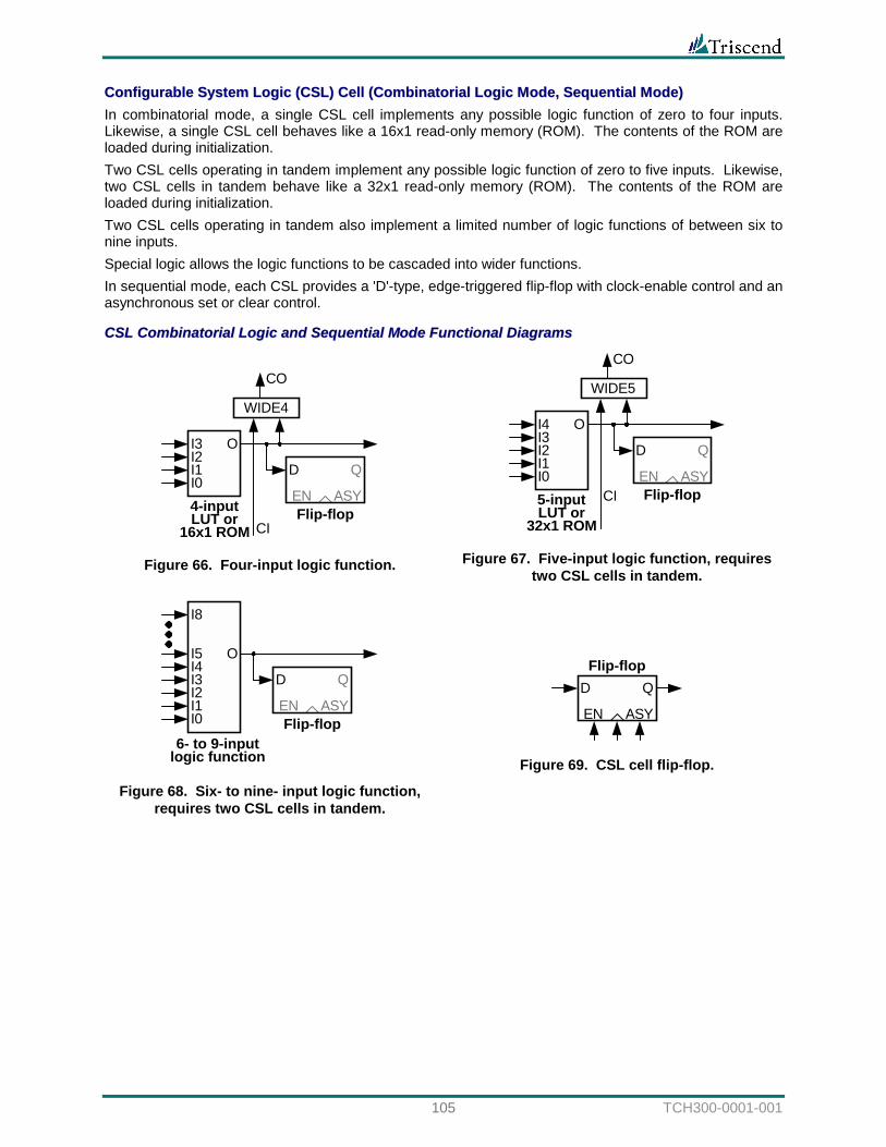
105 TCH300-0001-001
CCoonnffiigguurraabbllee SSyysstteemm LLooggiicc ((CCSSLL)) CCeellll ((CCoommbbiinnaattoorriiaall LLooggiicc MMooddee,, SSeeqquueennttiiaall MMooddee)) In combinatorial mode, a single CSL cell implements any possible logic function of zero to four inputs. Likewise, a single CSL cell behaves like a 16x1 read-only memory (ROM). The contents of the ROM are loaded during initialization. Two CSL cells operating in tandem implement any possible logic function of zero to five inputs. Likewise, two CSL cells in tandem behave like a 32x1 read-only memory (ROM). The contents of the ROM are loaded during initialization. Two CSL cells operating in tandem also implement a limited number of logic functions of between six to nine inputs. Special logic allows the logic functions to be cascaded into wider functions. In sequential mode, each CSL provides a 'D'-type, edge-triggered flip-flop with clock-enable control and an asynchronous set or clear control.
CCSSLL CCoommbbiinnaattoorriiaall LLooggiicc aanndd SSeeqquueennttiiaall MMooddee FFuunnccttiioonnaall DDiiaaggrraammss
4-inputLUT or
16x1 ROM
I3I2I1I0
O
Flip-flop
D
EN ASY
Q
WIDE4
CI
CO
Figure 66. Four-input logic function.
I4I3I2I1I0
O
5-inputLUT or
32x1 ROM
Flip-flop
D
EN ASY
Q
WIDE5
CI
CO
Figure 67. Five-input logic function, requires
two CSL cells in tandem.
I4I3I2I1I0
6- to 9-inputlogic function
I8
I5 O
Flip-flop
D
EN ASY
Q
Figure 68. Six- to nine- input logic function,
requires two CSL cells in tandem.
D
EN ASY
QFlip-flop
Figure 69. CSL cell flip-flop.
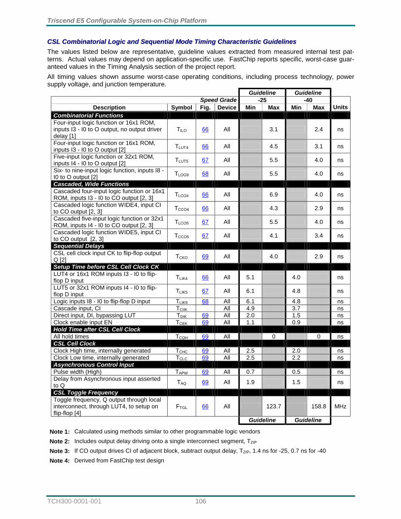
Triscend E5 Configurable System-on-Chip Platform
TCH300-0001-001 106
CCSSLL CCoommbbiinnaattoorriiaall LLooggiicc aanndd SSeeqquueennttiiaall MMooddee TTiimmiinngg CChhaarraacctteerriissttiicc GGuuiiddeelliinneess The values listed below are representative, guideline values extracted from measured internal test pat-terns. Actual values may depend on application-specific use. FastChip reports specific, worst-case guar-anteed values in the Timing Analysis section of the project report. All timing values shown assume worst-case operating conditions, including process technology, power supply voltage, and junction temperature.
Guideline Guideline Speed Grade -25 -40
Description Symbol Fig. Device Min Max Min Max Units Combinatorial Functions Four-input logic function or 16x1 ROM, inputs I3 - I0 to O output, no output driver delay [1]
TILO 66 All 3.1 2.4 ns
Four-input logic function or 16x1 ROM, inputs I3 - I0 to O output [2] TLUT4 66 All 4.5 3.1 ns
Five-input logic function or 32x1 ROM, inputs I4 - I0 to O output [2] TLUT5 67 All 5.5 4.0 ns
Six- to nine-input logic function, inputs I8 - I0 to O output [2] TLOG9 68 All 5.5 4.0 ns
Cascaded, Wide Functions Cascaded four-input logic function or 16x1 ROM, inputs I3 - I0 to CO output [2, 3] TLCO4 66 All 6.9 4.0 ns
Cascaded logic function WIDE4, input CI to CO output [2, 3] TCCO4 66 All 4.3 2.9 ns
Cascaded five-input logic function or 32x1 ROM, inputs I4 - I0 to CO output [2, 3] TLCO5 67 All 5.5 4.0 ns
Cascaded logic function WIDE5, input CI to CO output [2, 3] TCCO5 67 All 4.1 3.4 ns
Sequential Delays CSL cell clock input CK to flip-flop output Q [2] TCKO 69 All 4.0 2.9 ns
Setup Time before CSL Cell Clock CK LUT4 or 16x1 ROM inputs I3 - I0 to flip-flop D input TLIK4 66 All 5.1 4.0 ns
LUT5 or 32x1 ROM inputs I4 - I0 to flip-flop D input TLIK5 67 All 6.1 4.8 ns
Logic inputs I8 - I0 to flip-flop D input TLIK9 68 All 6.1 4.8 ns Cascade input, CI TCIIK All 4.9 3.7 ns Direct input, DI, bypassing LUT TDIK 69 All 2.0 1.5 ns Clock enable input EN TCEK 69 All 1.1 0.9 ns Hold Time after CSL Cell Clock All hold times TCQH 69 All 0 0 ns CSL Cell Clock Clock High time, internally generated TCHC 69 All 2.5 2.0 ns Clock Low time, internally generated TCLC 69 All 2.5 2.2 ns Asynchronous Control Input Pulse width (High) TAPW 69 All 0.7 0.5 ns Delay from Asynchronous input asserted to Q TAQ 69 All 1.9 1.5 ns
CSL Toggle Frequency Toggle frequency, Q output through local interconnect, through LUT4, to setup on flip-flop [4]
FTGL 66 All 123.7 158.8 MHz
Guideline Guideline
Note 1: Calculated using methods similar to other programmable logic vendors Note 2: Includes output delay driving onto a single interconnect segment, TZIP Note 3: If CO output drives CI of adjacent block, subtract output delay, TZIP, 1.4 ns for -25, 0.7 ns for -40 Note 4: Derived from FastChip test design
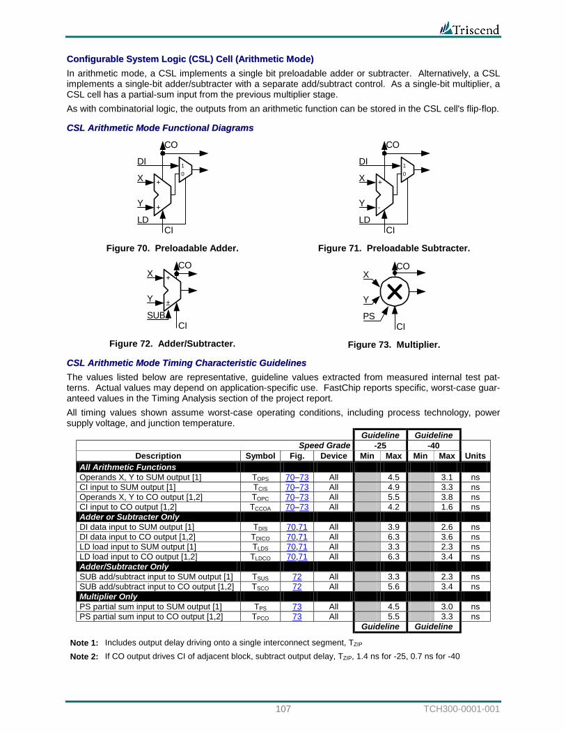
107 TCH300-0001-001
CCoonnffiigguurraabbllee SSyysstteemm LLooggiicc ((CCSSLL)) CCeellll ((AArriitthhmmeettiicc MMooddee)) In arithmetic mode, a CSL implements a single bit preloadable adder or subtracter. Alternatively, a CSL implements a single-bit adder/subtracter with a separate add/subtract control. As a single-bit multiplier, a CSL cell has a partial-sum input from the previous multiplier stage. As with combinatorial logic, the outputs from an arithmetic function can be stored in the CSL cell's flip-flop.
CCSSLL AArriitthhmmeettiicc MMooddee FFuunnccttiioonnaall DDiiaaggrraammss
10
+
+X
Y
LD
DI
CI
CO
Figure 70. Preloadable Adder.
10
-
+
CO
CILD
Y
X
DI
Figure 71. Preloadable Subtracter.
±
+CO
CISUB
Y
X
Figure 72. Adder/Subtracter.
CO
CI
X
Y
PS
Figure 73. Multiplier.
CCSSLL AArriitthhmmeettiicc MMooddee TTiimmiinngg CChhaarraacctteerriissttiicc GGuuiiddeelliinneess The values listed below are representative, guideline values extracted from measured internal test pat-terns. Actual values may depend on application-specific use. FastChip reports specific, worst-case guar-anteed values in the Timing Analysis section of the project report. All timing values shown assume worst-case operating conditions, including process technology, power supply voltage, and junction temperature.
Guideline Guideline Speed Grade -25 -40
Description Symbol Fig. Device Min Max Min Max Units All Arithmetic Functions Operands X, Y to SUM output [1] TOPS 70–73 All 4.5 3.1 ns CI input to SUM output [1] TCIS 70–73 All 4.9 3.3 ns Operands X, Y to CO output [1,2] TOPC 70–73 All 5.5 3.8 ns CI input to CO output [1,2] TCCOA 70–73 All 4.2 1.6 ns Adder or Subtracter Only DI data input to SUM output [1] TDIS 70,71 All 3.9 2.6 ns DI data input to CO output [1,2] TDICO 70,71 All 6.3 3.6 ns LD load input to SUM output [1] TLDS 70,71 All 3.3 2.3 ns LD load input to CO output [1,2] TLDCO 70,71 All 6.3 3.4 ns Adder/Subtracter Only SUB add/subtract input to SUM output [1] TSUS 72 All 3.3 2.3 ns SUB add/subtract input to CO output [1,2] TSCO 72 All 5.6 3.4 ns Multiplier Only PS partial sum input to SUM output [1] TPS 73 All 4.5 3.0 ns PS partial sum input to CO output [1,2] TPCO 73 All 5.5 3.3 ns Guideline Guideline
Note 1: Includes output delay driving onto a single interconnect segment, TZIP Note 2: If CO output drives CI of adjacent block, subtract output delay, TZIP, 1.4 ns for -25, 0.7 ns for -40
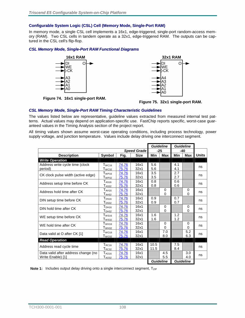
Triscend E5 Configurable System-on-Chip Platform
TCH300-0001-001 108
CCoonnffiigguurraabbllee SSyysstteemm LLooggiicc ((CCSSLL)) CCeellll ((MMeemmoorryy MMooddee,, SSiinnggllee--PPoorrtt RRAAMM)) In memory mode, a single CSL cell implements a 16x1, edge-triggered, single-port random-access mem-ory (RAM). Two CSL cells in tandem operate as a 32x1, edge-triggered RAM. The outputs can be cap-tured in the CSL cell's flip-flop.
CCSSLL MMeemmoorryy MMooddee,, SSiinnggllee--PPoorrtt RRAAMM FFuunnccttiioonnaall DDiiaaggrraammss
16x1 RAM
A3A2A1A0
DIWECK
O
Figure 74. 16x1 single-port RAM.
32x1 RAM
A4A3A2
DIWECK
O
A1A0
Figure 75. 32x1 single-port RAM.
CCSSLL MMeemmoorryy MMooddee,, SSiinnggllee--PPoorrtt RRAAMM TTiimmiinngg CChhaarraacctteerriissttiicc GGuuiiddeelliinneess The values listed below are representative, guideline values extracted from measured internal test pat-terns. Actual values may depend on application-specific use. FastChip reports specific, worst-case guar-anteed values in the Timing Analysis section of the project report. All timing values shown assume worst-case operating conditions, including process technology, power supply voltage, and junction temperature. Values include delay driving one interconnect segment.
Guideline Guideline Speed Grade -25 -40
Description Symbol Fig. Size Min Max Min Max Units Write Operation Address write cycle time (clock period)
TWC16 TWC32
74,76 75,76
16x1 32x1
5.6 5.6 4.1
4.1 ns
CK clock pulse width (active edge) TWP16 TWP32
74,76 75,76
16x1 32x1
3.5 3.5 2.7
2.7 ns
Address setup time before CK TAS16 TAS32
74,76 75,76
16x1 32x1
0.8 0.8 0.6
0.6 ns
Address hold time after CK TAH16 TAH32
74,76 75,76
16x1 32x1 0
0 0 0 ns
DIN setup time before CK TDS16 TDS32
74,76 75,76
16x1 32x1
0.9 0.9 0.7
0.7 ns
DIN hold time after CK TDH16 TDH32
74,76 75,76
16x1 32x1 0
0 0 0 ns
WE setup time before CK TWS16 TWS32
74,76 75,76
16x1 32x1
1.6 1.6 1.2
1.2 ns
WE hold time after CK TWH16 TWH32
74,76 75,76
16x1 32x1 0
0 0 0 ns
Data valid at O after CK [1] TWO16 TWO32
74,76 75,76
16x1 32x1 7.0
8.0 5.2 6.3 ns
Read Operation
Address read cycle time TRC16 TRC32
74,76 75,76
16x1 32x1
10.5 11.5 7.5
8.4 ns
Data valid after address change (no Write Enable) [1]
TAO16 TAO32
74,76 75,76
16x1 32x1 4.5
5.5 3.0 4.0 ns
Guideline Guideline
Note 1: Includes output delay driving onto a single interconnect segment, TZIP
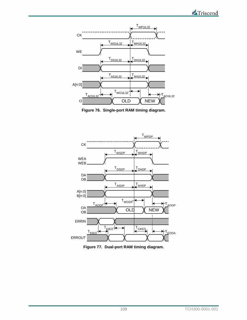
109 TCH300-0001-001
CK
WE
TWS16,32
TWP16,32
TWH16,32
TDS16,32 TDH16,32
TAS16,32 TAH16,32
TAO16,32 TAO16,32TWO16,32
A[n:0]
DI
OLD NEWO
Figure 76. Single-port RAM timing diagram.
WEAWEB
TWSDP
TWPDP
TWHDP
TDSDP TDHDP
TASDP TAHDP
TAODPTWODP
A[n:0]B[n:0]
DADB
OLD NEWOAOB
CK
ERRIN
ERROUT
TEODA
TAODP
TEIEO
TEIEO TCKEO
Figure 77. Dual-port RAM timing diagram.
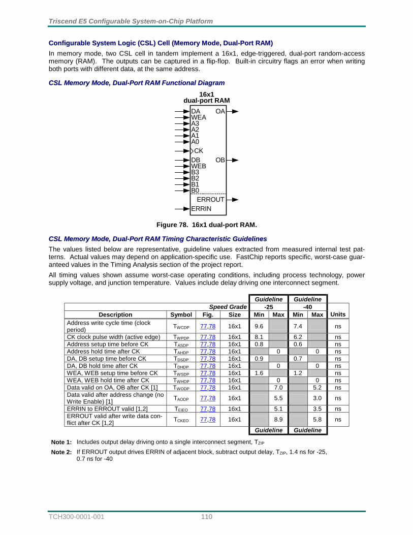
Triscend E5 Configurable System-on-Chip Platform
TCH300-0001-001 110
CCoonnffiigguurraabbllee SSyysstteemm LLooggiicc ((CCSSLL)) CCeellll ((MMeemmoorryy MMooddee,, DDuuaall--PPoorrtt RRAAMM)) In memory mode, two CSL cell in tandem implement a 16x1, edge-triggered, dual-port random-access memory (RAM). The outputs can be captured in a flip-flop. Built-in circuitry flags an error when writing both ports with different data, at the same address.
CCSSLL MMeemmoorryy MMooddee,, DDuuaall--PPoorrtt RRAAMM FFuunnccttiioonnaall DDiiaaggrraamm
CK
A3A2A1A0
DAWEA
WEBB3B2B1B0
DB
ERRIN
OA
OB
ERROUT
16x1dual-port RAM
Figure 78. 16x1 dual-port RAM.
CCSSLL MMeemmoorryy MMooddee,, DDuuaall--PPoorrtt RRAAMM TTiimmiinngg CChhaarraacctteerriissttiicc GGuuiiddeelliinneess The values listed below are representative, guideline values extracted from measured internal test pat-terns. Actual values may depend on application-specific use. FastChip reports specific, worst-case guar-anteed values in the Timing Analysis section of the project report. All timing values shown assume worst-case operating conditions, including process technology, power supply voltage, and junction temperature. Values include delay driving one interconnect segment.
Guideline Guideline Speed Grade -25 -40
Description Symbol Fig. Size Min Max Min Max Units Address write cycle time (clock period) TWCDP 77,78 16x1 9.6 7.4 ns
CK clock pulse width (active edge) TWPDP 77,78 16x1 8.1 6.2 ns Address setup time before CK TASDP 77,78 16x1 0.8 0.6 ns Address hold time after CK TAHDP 77,78 16x1 0 0 ns DA, DB setup time before CK TDSDP 77,78 16x1 0.9 0.7 ns DA, DB hold time after CK TDHDP 77,78 16x1 0 0 ns WEA, WEB setup time before CK TWSDP 77,78 16x1 1.6 1.2 ns WEA, WEB hold time after CK TWHDP 77,78 16x1 0 0 ns Data valid on OA, OB after CK [1] TWODP 77,78 16x1 7.0 5.2 ns Data valid after address change (no Write Enable) [1] TAODP 77,78 16x1 5.5 3.0 ns
ERRIN to ERROUT valid [1,2] TEIEO 77,78 16x1 5.1 3.5 ns ERROUT valid after write data con-flict after CK [1,2] TCKEO 77,78 16x1 8.9 5.8 ns
Guideline Guideline
Note 1: Includes output delay driving onto a single interconnect segment, TZIP Note 2: If ERROUT output drives ERRIN of adjacent block, subtract output delay, TZIP, 1.4 ns for -25,
0.7 ns for -40
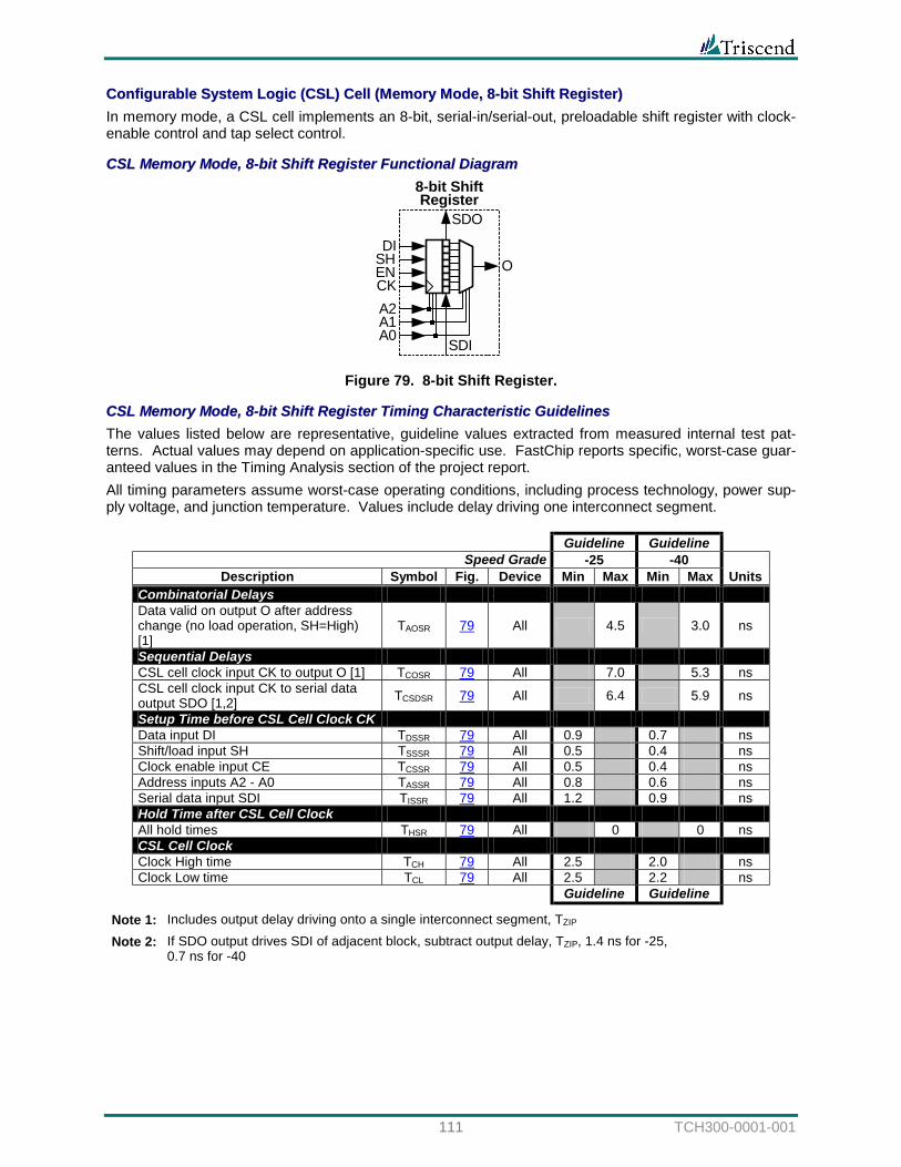
111 TCH300-0001-001
CCoonnffiigguurraabbllee SSyysstteemm LLooggiicc ((CCSSLL)) CCeellll ((MMeemmoorryy MMooddee,, 88--bbiitt SShhiifftt RReeggiisstteerr)) In memory mode, a CSL cell implements an 8-bit, serial-in/serial-out, preloadable shift register with clock-enable control and tap select control.
CCSSLL MMeemmoorryy MMooddee,, 88--bbiitt SShhiifftt RReeggiisstteerr FFuunnccttiioonnaall DDiiaaggrraamm
SH
A2A1A0
SDI
DI
CK
SDO
EN O
8-bit ShiftRegister
Figure 79. 8-bit Shift Register.
CCSSLL MMeemmoorryy MMooddee,, 88--bbiitt SShhiifftt RReeggiisstteerr TTiimmiinngg CChhaarraacctteerriissttiicc GGuuiiddeelliinneess The values listed below are representative, guideline values extracted from measured internal test pat-terns. Actual values may depend on application-specific use. FastChip reports specific, worst-case guar-anteed values in the Timing Analysis section of the project report. All timing parameters assume worst-case operating conditions, including process technology, power sup-ply voltage, and junction temperature. Values include delay driving one interconnect segment.
Guideline Guideline Speed Grade -25 -40
Description Symbol Fig. Device Min Max Min Max Units Combinatorial Delays Data valid on output O after address change (no load operation, SH=High) [1]
TAOSR 79 All 4.5 3.0 ns
Sequential Delays CSL cell clock input CK to output O [1] TCOSR 79 All 7.0 5.3 ns CSL cell clock input CK to serial data output SDO [1,2] TCSDSR 79 All 6.4 5.9 ns
Setup Time before CSL Cell Clock CK Data input DI TDSSR 79 All 0.9 0.7 ns Shift/load input SH TSSSR 79 All 0.5 0.4 ns Clock enable input CE TCSSR 79 All 0.5 0.4 ns Address inputs A2 - A0 TASSR 79 All 0.8 0.6 ns Serial data input SDI TISSR 79 All 1.2 0.9 ns Hold Time after CSL Cell Clock All hold times THSR 79 All 0 0 ns CSL Cell Clock Clock High time TCH 79 All 2.5 2.0 ns Clock Low time TCL 79 All 2.5 2.2 ns
Guideline Guideline
Note 1: Includes output delay driving onto a single interconnect segment, TZIP Note 2: If SDO output drives SDI of adjacent block, subtract output delay, TZIP, 1.4 ns for -25,
0.7 ns for -40
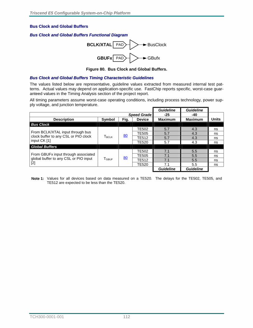
Triscend E5 Configurable System-on-Chip Platform
TCH300-0001-001 112
BBuuss CClloocckk aanndd GGlloobbaall BBuuffffeerrss
BBuuss CClloocckk aanndd GGlloobbaall BBuuffffeerrss FFuunnccttiioonnaall DDiiaaggrraamm
PADBCLK/XTAL
PADGBUFx
BusClock
GBufx
Figure 80. Bus Clock and Global Buffers.
BBuuss CClloocckk aanndd GGlloobbaall BBuuffffeerrss TTiimmiinngg CChhaarraacctteerriissttiicc GGuuiiddeelliinneess The values listed below are representative, guideline values extracted from measured internal test pat-terns. Actual values may depend on application-specific use. FastChip reports specific, worst-case guar-anteed values in the Timing Analysis section of the project report. All timing parameters assume worst-case operating conditions, including process technology, power sup-ply voltage, and junction temperature. Guideline Guideline
Speed Grade -25 -40 Description Symbol Fig. Device Maximum Maximum Units
Bus Clock TE502 5.7 4.3 ns TE505 5.7 4.3 ns TE512 5.7 4.3 ns
From BCLK/XTAL input through bus clock buffer to any CSL or PIO clock input CK [1]
TBCLK 80
TE520 5.7 4.3 ns Global Buffers
TE502 7.1 5.5 ns TE505 7.1 5.5 ns TE512 7.1 5.5 ns
From GBUFx input through associated global buffer to any CSL or PIO input [2]
TGBUF 80
TE520 7.1 5.5 ns Guideline Guideline
Note 1: Values for all devices based on data measured on a TE520. The delays for the TE502, TE505, and
TE512 are expected to be less than the TE520.
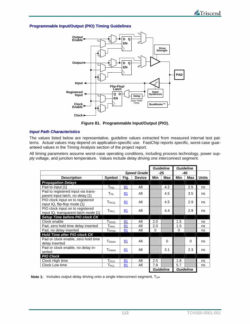
113 TCH300-0001-001
PPrrooggrraammmmaabbllee IInnppuutt//OOuuttppuutt ((PPIIOO)) TTiimmiinngg GGuuiiddeelliinneess
QEN
D
Flip-Flop/Latch
Input
RegisteredInput
Clock
ClockEnable
InputHysteresis
PAD
BusMinder™
OutputEnable
DriveStrength
Output
DelayZero Hold
Time
DEN
Q
DEN
Q
Figure 81. Programmable Input/Output (PIO).
IInnppuutt PPaatthh CChhaarraacctteerriissttiiccss The values listed below are representative, guideline values extracted from measured internal test pat-terns. Actual values may depend on application-specific use. FastChip reports specific, worst-case guar-anteed values in the Timing Analysis section of the project report. All timing parameters assume worst-case operating conditions, including process technology, power sup-ply voltage, and junction temperature. Values include delay driving one interconnect segment.
Guideline Guideline Speed Grade -25 -40
Description Symbol Fig. Device Min Max Min Max Units Propagation Delays Pad to input [1] TPID 81 All 4.2 2.5 ns Pad to registered input via trans-parent input latch, no delay [1] TPIL 81 All 4.5 3.5 ns
PIO clock input on to registered input IQ, flip-flop mode [1] TPICQ 81 All 4.5 2.9 ns
PIO clock input on to registered input IQ, transparent latch mode [1] TPICL 81 All 4.4 2.9 ns
Setup Time before PIO clock CK Clock enable TPENS 81 All 2.0 1.5 ns Pad, zero hold time delay inserted TPPS 81 All 2.0 1.5 ns Pad, no delay inserted TPPSN 81 All 0 0 ns Hold Time after PIO clock CK Pad or clock enable, zero hold time delay inserted TPENH 81 All 0 0 ns
Pad or clock enable, no delay in-serted TPNHN 81 All 3.1 2.3 ns
PIO Clock Clock High time TPCH 81 All 2.5 1.8 ns Clock Low time TPCL 81 All 7.8 5.7 ns Guideline Guideline
Note 1: Includes output delay driving onto a single interconnect segment, TZIP
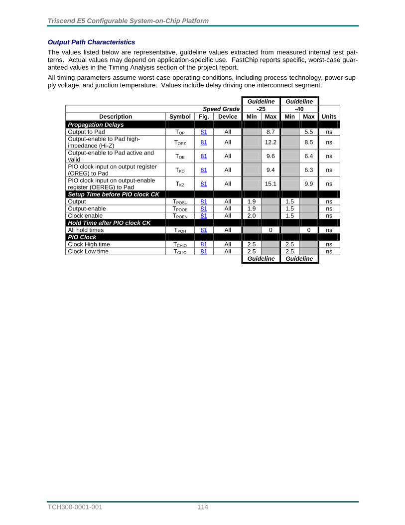
Triscend E5 Configurable System-on-Chip Platform
TCH300-0001-001 114
OOuuttppuutt PPaatthh CChhaarraacctteerriissttiiccss The values listed below are representative, guideline values extracted from measured internal test pat-terns. Actual values may depend on application-specific use. FastChip reports specific, worst-case guar-anteed values in the Timing Analysis section of the project report. All timing parameters assume worst-case operating conditions, including process technology, power sup-ply voltage, and junction temperature. Values include delay driving one interconnect segment.
Guideline Guideline Speed Grade -25 -40
Description Symbol Fig. Device Min Max Min Max Units Propagation Delays Output to Pad TOP 81 All 8.7 5.5 ns Output-enable to Pad high-impedance (Hi-Z) TOPZ 81 All 12.2 8.5 ns
Output-enable to Pad active and valid TOE 81 All 9.6 6.4 ns
PIO clock input on output register (OREG) to Pad TKO 81 All 9.4 6.3 ns
PIO clock input on output-enable register (OEREG) to Pad TKZ 81 All 15.1 9.9 ns
Setup Time before PIO clock CK Output TPOSU 81 All 1.9 1.5 ns Output-enable TPOOE 81 All 1.9 1.5 ns Clock enable TPOEN 81 All 2.0 1.5 ns Hold Time after PIO clock CK All hold times TPQH 81 All 0 0 ns PIO Clock Clock High time TCHIO 81 All 2.5 2.5 ns Clock Low time TCLIO 81 All 2.5 2.5 ns Guideline Guideline
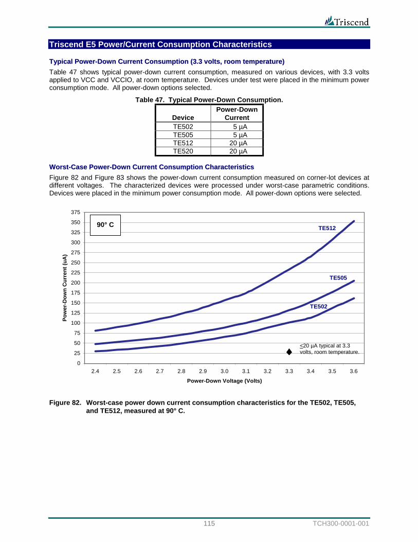
115 TCH300-0001-001
Triscend E5 Power/Current Consumption Characteristics
TTyyppiiccaall PPoowweerr--DDoowwnn CCuurrrreenntt CCoonnssuummppttiioonn ((33..33 vvoollttss,, rroooomm tteemmppeerraattuurree)) Table 47 shows typical power-down current consumption, measured on various devices, with 3.3 volts applied to VCC and VCCIO, at room temperature. Devices under test were placed in the minimum power consumption mode. All power-down options selected.
Table 47. Typical Power-Down Consumption.
Device Power-Down
Current TE502 5 µA TE505 5 µA TE512 20 µA TE520 20 µA
WWoorrsstt--CCaassee PPoowweerr--DDoowwnn CCuurrrreenntt CCoonnssuummppttiioonn CChhaarraacctteerriissttiiccss Figure 82 and Figure 83 shows the power-down current consumption measured on corner-lot devices at different voltages. The characterized devices were processed under worst-case parametric conditions. Devices were placed in the minimum power consumption mode. All power-down options were selected.
0
25
50
75
100
125
150
175
200
225
250
275
300
325
350
375
2.4 2.5 2.6 2.7 2.8 2.9 3.0 3.1 3.2 3.3 3.4 3.5 3.6
Power-Down Voltage (Volts)
Pow
er-D
own
Cur
rent
(uA
)
TE512
TE505
TE502
Figure 82. Worst-case power down current consumption characteristics for the TE502, TE505,
and TE512, measured at 90° C.
<20 µA typical at 3.3 volts, room temperature.
90° C
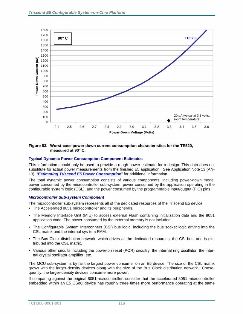
Triscend E5 Configurable System-on-Chip Platform
TCH300-0001-001 116
0100200300400500600700800900
100011001200130014001500160017001800
2.4 2.5 2.6 2.7 2.8 2.9 3.0 3.1 3.2 3.3 3.4 3.5 3.6
Power-Down Voltage (Volts)
Pow
er-D
own
Cur
rent
(uA
)TE520
Figure 83. Worst-case power down current consumption characteristics for the TE520,
measured at 90° C.
TTyyppiiccaall DDyynnaammiicc PPoowweerr CCoonnssuummppttiioonn CCoommppoonneenntt EEssttiimmaatteess This information should only be used to provide a rough power estimate for a design. This data does not substitute for actual power measurements from the finished E5 application. See Application Note 13 (AN-13), “Estimating Triscend E5 Power Consumption” for additional information. The total dynamic power consumption consists of various components, including power-down mode, power consumed by the microcontroller sub-system, power consumed by the application operating in the configurable system logic (CSL), and the power consumed by the programmable input/output (PIO) pins.
MMiiccrrooccoonnttrroolllleerr SSuubb--ssyysstteemm CCoommppoonneenntt The microcontroller sub-system represents all of the dedicated resources of the Triscend E5 device. • The Accelerated 8051 microcontroller and its peripherals.
• The Memory Interface Unit (MIU) to access external Flash containing initialization data and the 8051 application code. The power consumed by the external memory is not included.
• The Configurable System Interconnect (CSI) bus logic, including the bus socket logic driving into the CSL matrix and the internal sys-tem RAM.
• The Bus Clock distribution network, which drives all the dedicated resources, the CSI bus, and is dis-tributed into the CSL matrix.
• Various other circuits including the power-on reset (POR) circuitry, the internal ring oscillator, the inter-nal crystal oscillator amplifier, etc.
The MCU sub-system is by far the largest power consumer on an E5 device. The size of the CSL matrix grows with the larger-density devices along with the size of the Bus Clock distribution network. Conse-quently, the larger-density devices consume more power. If comparing against the original 8051microcontroller, consider that the accelerated 8051 microcontroller embedded within an E5 CSoC device has roughly three times more performance operating at the same
20 µA typical at 3.3 volts, room temperature.
90° C
117 TCH300-0001-001
frequency. Consequently, the accelerated 8051 microcontroller within an E5 device can operate at one-third the clock frequency while maintaining the same overall performance as the original 8051 design.
20mWFrequencyDynamicMCU_Power typical) C,70 volts, (3.6 O +•=
Dynamic is the microcontroller sub-system power consumption from Table 48. Frequency is the bus clock frequency in MHz.
Table 48. Typical microcontroller sub-system dynamic power consumption at 3.6 volts, 70° C.
Device Dynamic Power Consumption Units
TE502* 4.5 TE505* 6.7 TE512* 12.7 TE520* 18.0
mW/MHz
*estimate, based on measured data from TE520.
CCSSLL PPoowweerr CCoommppoonneenntt The power consumed by the configurable system logic (CSL) portion of the CSoC device is the sum of all the CSL cells utilized in the application. Not every CSL cell switches on every clock cycle. The switch factor, k, describes the switching activity for the CSL cell. In a typical application, only about 5% to 30% of the cells switch on a given clock edge. The Frequency is the clock frequency at the CSL cell clock input or the frequency at which a group of CSL cells changes, in MHz. It is easiest to compute the total CSL power component by examining the individual clock domains within an application.
∑ ••= Frequency0.15mW/MHzCSL_Power typical) C,70 volts, (3.6 O k
PPIIOO PPoowweerr CCoommppoonneenntt The power consumed by the programmable input/output (PIO) cells on the CSoC device is the sum of all the PIO cells that are configured as outputs utilized in the application. Not every PIO cell switches on every clock cycle. The switch factor, k, describes the switching activity for the PIO cell. In a typical appli-cation, only about 5% to 30% of the cells switch on a given clock edge. The Frequency is the frequency at which a group of PIO cells changes, in MHz.. It is easiest to compute the total PIO power component by examining the individual clock domains within an application. The PIO dynamic power depends on whether the PIO drives 4 mA or 12 mA, as shown in Table 49.
∑ ••= FrequencycPIO_DynamiPIO_Power typical) C,70 volts, (3.6 O k
Table 49. Typical PIO output pin power consumption at 3.6 volts, 70° C. Drive
Strength Dynamic Power Consumption Units
4 mA 1.3 12 mA 2.6
mW/MHz
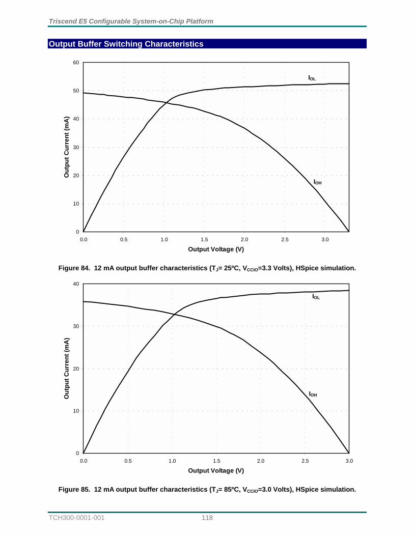
Triscend E5 Configurable System-on-Chip Platform
TCH300-0001-001 118
Output Buffer Switching Characteristics
0
10
20
30
40
50
60
0.0 0.5 1.0 1.5 2.0 2.5 3.0
Output Voltage (V)
Out
put C
urre
nt (m
A)
IOL
IOH
Figure 84. 12 mA output buffer characteristics (TJ= 25ºC, VCCIO=3.3 Volts), HSpice simulation.
0
10
20
30
40
0.0 0.5 1.0 1.5 2.0 2.5 3.0
Output Voltage (V)
Out
put C
urre
nt (m
A)
IOL
IOH
Figure 85. 12 mA output buffer characteristics (TJ= 85ºC, VCCIO=3.0 Volts), HSpice simulation.
119 TCH300-0001-001
Appendix A: E5 Instruction Timing Table 50 shows the instruction timing for the E5’s embedded and accelerated 8051 microcontroller. The table also shows the performance of the E5 versus the original 8051 and the 80C320. All E5 instruction fetches are affected by the read timing settings in the Memory Interface Unit. The "E5 Clock Cycles" val-ues in the table below assume an external memory device fast enough to perform a four-cycle fetch at the bus clock frequency, without wait-states. The number of E5 machine cycles is not affected. All E5 instruction timing is potentially affected by wait-states on the bus. Wait-states may affect the num-ber of E5 clock cycles required to complete an instruction. The number of machine cycles is not affected. The original 8051 did not support wait-states. The E5 supports an op-code 'A5' instruction, which was not available on the original 8032. This is a soft-ware breakpoint function. The timing for this E5 instruction has not been characterized.
Table 50. E5 Instruction Timing.
Instruction Hex Code Bytes Machine
Cycles E5 Clock Cycles
8051 Clock Cycles
E5 vs. 8051 Speed Ratio
80C320 Clock Cycles
E5 vs. 80C320
Speed Ratio NOP 00 1 1 4 12 3 4 1 ADD A, RO 28 1 1 4 12 3 4 1 ADD A, R1 29 1 1 4 12 3 4 1 ADD A, R2 2A 1 1 4 12 3 4 1 ADD A, R3 2B 1 1 4 12 3 4 1 ADD A, R4 2C 1 1 4 12 3 4 1 ADD A, R5 2D 1 1 4 12 3 4 1 ADD A, R6 2E 1 1 4 12 3 4 1 ADD A, R7 2F 1 1 4 12 3 4 1 ADD A, @RO 26 1 1 4 12 3 4 1 ADD A, @R1 27 1 1 4 12 3 4 1 ADD A, direct 25 2 2 8 12 1.5 8 1 ADD A, #data 24 2 2 8 12 1.5 8 1 ADDC A, RO 38 1 1 4 12 3 4 1 ADDC A, R1 39 1 1 4 12 3 4 1 ADDC A, R2 3A 1 1 4 12 3 4 1 ADDC A, R3 3B 1 1 4 12 3 4 1 ADDC A, R4 3C 1 1 4 12 3 4 1 ADDC A, R5 3D 1 1 4 12 3 4 1 ADDC A, R6 3E 1 1 4 12 3 4 1 ADDC A, R7 3F 1 1 4 12 3 4 1 ADDC A, @R0 36 1 1 4 12 3 4 1 ADDC A, @R1 37 1 1 4 12 3 4 1 ADDC A, direct 35 2 2 8 12 1.5 8 1 ADDC A, #data 34 2 2 8 12 1.5 8 1 SUBB A, R0 48 1 1 4 12 3 4 1 SUBB A, R1 49 1 1 4 12 3 4 1 SUBB A, R2 4A 1 1 4 12 3 4 1 SUBB A, R3 4B 1 1 4 12 3 4 1 SUBB A, R4 4C 1 1 4 12 3 4 1 SUBB A, R5 4D 1 1 4 12 3 4 1 SUBB A, R6 4E 1 1 4 12 3 4 1 SUBB A, R7 4F 1 1 4 12 3 4 1 SUBB A, @R0 46 1 1 4 12 3 4 1 SUBB A, @R1 47 1 1 4 12 3 4 1 SUBB A, direct 45 2 2 8 12 1.5 8 1 SUBB A, #data 44 2 2 8 12 1.5 8 1 INC A 04 1 1 4 12 3 4 1 INC R0 08 1 1 4 12 3 4 1 INC R1 09 1 1 4 12 3 4 1 INC R2 0A 1 1 4 12 3 4 1 INC R3 0B 1 1 4 12 3 4 1 INC R4 0C 1 1 4 12 3 4 1
Triscend E5 Configurable System-on-Chip Platform
TCH300-0001-001 120
Instruction Hex Code Bytes Machine
Cycles E5 Clock Cycles
8051 Clock Cycles
E5 vs. 8051 Speed Ratio
80C320 Clock Cycles
E5 vs. 80C320
Speed Ratio INC R5 0D 1 1 4 12 3 4 1 INC R6 0E 1 1 4 12 3 4 1 INC R7 0F 1 1 4 12 3 4 1 INC @R0 06 1 1 4 12 3 4 1 INC @R1 07 1 1 4 12 3 4 1 INC direct 05 2 2 8 12 1.5 8 1 INC DPTR A3 1 2 8 24 3 12 1.5 DEC A 14 1 1 4 12 3 4 1 DEC R0 18 1 1 4 12 3 4 1 DEC R1 19 1 1 4 12 3 4 1 DEC R2 1A 1 1 4 12 3 4 1 DEC R3 1B 1 1 4 12 3 4 1 DEC R4 1C 1 1 4 12 3 4 1 DEC R5 1D 1 1 4 12 3 4 1 DEC R6 1E 1 1 4 12 3 4 1 DEC R7 1F 1 1 4 12 3 4 1 DEC @R0 16 1 1 4 12 3 4 1 DEC @R1 17 1 1 4 12 3 4 1 DEC direct 15 2 2 8 12 1.5 8 1 Software Breakpoint A5 1 ? ? - - - 1 MUL AB A4 1 5 20 48 2.4 20 1 DIV AB 84 1 5 20 48 2.4 20 1 DA A D4 1 1 4 12 3 4 1 ANL A, RO 58 1 1 4 12 3 4 1 ANL A, R1 59 1 1 4 12 3 4 1 ANL A, R2 5A 1 1 4 12 3 4 1 ANL A, R3 5B 1 1 4 12 3 4 1 ANL A, R4 5C 1 1 4 12 3 4 1 ANL A, R5 5D 1 1 4 12 3 4 1 ANL A, R6 5E 1 1 4 12 3 4 1 ANL A, R7 5F 1 1 4 12 3 4 1 ANL A, @R0 56 1 1 4 12 3 4 1 ANL A, @R1 57 1 1 4 12 3 4 1 ANL A, direct 55 2 2 8 12 1.5 8 1 ANL A, #data 54 2 2 8 12 1.5 8 1 ANL direct A 52 2 2 8 12 1.5 8 1 ANL direct, #data 53 3 3 12 24 2 12 1 ORL A, R0 48 1 1 4 12 3 4 1 ORL A, R1 49 1 1 4 12 3 4 1 ORL A, R2 4A 1 1 4 12 3 4 1 ORL A, R3 4B 1 1 4 12 3 4 1 ORL A, R4 4C 1 1 4 12 3 4 1 ORL A, R5 4D 1 1 4 12 3 4 1 ORL A, R6 4E 1 1 4 12 3 4 1 ORL A, R7 4F 1 1 4 12 3 4 1 ORL A, R7 4F 1 1 4 12 3 4 1 ORL A, @R0 46 1 1 4 12 3 4 1 ORL A, @R1 47 1 1 4 12 3 4 1 ORL A, direct 45 2 2 8 12 1.5 8 1 ORL A, #data 44 2 2 8 12 1.5 8 1 ORL direct, A 42 2 2 8 12 1.5 8 1 ORL direct, #data 43 3 3 12 24 2 12 1 XRL A, R0 68 1 1 4 12 3 4 1 XRL A, R1 69 1 1 4 12 3 4 1 XRL A, R2 6A 1 1 4 12 3 4 1 XRL A, R3 6B 1 1 4 12 3 4 1 XRL A, R4 6C 1 1 4 12 3 4 1
121 TCH300-0001-001
Instruction Hex Code Bytes Machine
Cycles E5 Clock Cycles
8051 Clock Cycles
E5 vs. 8051 Speed Ratio
80C320 Clock Cycles
E5 vs. 80C320
Speed Ratio XRL A, R5 6D 1 1 4 12 3 4 1 XRL A, R6 6E 1 1 4 12 3 4 1 XRL A, R7 6F 1 1 4 12 3 4 1 XRL A, @R0 66 1 1 4 12 3 4 1 XRL A, @R1 67 1 1 4 12 3 4 1 XRL A, direct 65 2 2 8 12 1.5 8 1 XRL A, #data 64 2 2 8 12 1.5 8 1 XRL direct, A 62 2 2 8 12 1.5 8 1 XRL direct, #data 63 3 3 12 24 2 12 1 CLR A E4 1 1 4 12 3 4 1 CPL A F4 1 1 4 12 3 4 1 RL A 23 1 1 4 12 3 4 1 RLC A 33 1 1 4 12 3 4 1 RR A 03 1 1 4 12 3 4 1 RRC A 13 1 1 4 12 3 4 1 SWAP A C4 1 1 4 12 3 4 1 MOV A, R0 E8 1 1 4 12 3 4 1 MOV A, R1 E9 1 1 4 12 3 4 1 MOV A, R2 EA 1 1 4 12 3 4 1 MOV A, R3 EB 1 1 4 12 3 4 1 MOV A, R4 EC 1 1 4 12 3 4 1 MOV A, R5 ED 1 1 4 12 3 4 1 MOV A, R6 EE 1 1 4 12 3 4 1 MOV A, R7 EF 1 1 4 12 3 4 1 MOV A, @R0 E6 1 1 4 12 3 4 1 MOV A, @R1 E7 1 1 4 12 3 4 1 MOV A, direct E5 2 2 8 12 1.5 8 1 MOV A, #data 74 2 2 8 12 1.5 8 1 MOV RO, A F8 1 1 4 12 3 4 1 MOV R1, A F9 1 1 4 12 3 4 1 MOV R2, A FA 1 1 4 12 3 4 1 MOV R3, A FB 1 1 4 12 3 4 1 MOV R4, A FC 1 1 4 12 3 4 1 MOV R5, A FD 1 1 4 12 3 4 1 MOV R6, A FE 1 1 4 12 3 4 1 MOV R7, A FF 1 1 4 12 3 4 1 MOV R0, direct A8 2 2 8 12 1.5 8 1 MOV R1, direct A9 2 2 8 12 1.5 8 1 MOV R2, direct AA 2 2 8 12 1.5 8 1 MOV R3, direct AB 2 2 8 12 1.5 8 1 MOV R4, direct AC 2 2 8 12 1.5 8 1 MOV R5, direct AD 2 2 8 12 1.5 8 1 MOV R6, direct AE 2 2 8 12 1.5 8 1 MOV R7, direct AF 2 2 8 12 1.5 8 1 MOV RO, #data 78 2 2 8 12 1.5 8 1 MOV RO, #data 78 2 2 8 12 1.5 8 1 MOV R1, #data 79 2 2 8 12 1.5 8 1 MOV R2, #data 7A 2 2 8 12 1.5 8 1 MOV R3, #data 7B 2 2 8 12 1.5 8 1 MOV R4, #data 7C 2 2 8 12 1.5 8 1 MOV R5, #data 7D 2 2 8 12 1.5 8 1 MOV R6, #data 7E 2 2 8 12 1.5 8 1 MOV R7, #data 7F 2 2 8 12 1.5 8 1 MOV @RO, A F6 1 1 4 12 3 4 1 MOV @R1, A F7 1 1 4 12 3 4 1 MOV @RO, direct A6 2 2 8 12 1.5 8 1 MOV @R1, direct A7 2 2 8 12 1.5 8 1
Triscend E5 Configurable System-on-Chip Platform
TCH300-0001-001 122
Instruction Hex Code Bytes Machine
Cycles E5 Clock Cycles
8051 Clock Cycles
E5 vs. 8051 Speed Ratio
80C320 Clock Cycles
E5 vs. 80C320
Speed Ratio MOV @RO, #data 76 2 2 8 12 1.5 8 1 MOV @R1, #data 77 2 2 8 12 1.5 8 1 MOV direct, A F5 2 2 8 12 1.5 8 1 MOV direct, RO 88 2 2 8 12 1.5 8 1 MOV direct, R1 89 2 2 8 12 1.5 8 1 MOV direct, R2 8A 2 2 8 12 1.5 8 1 MOV direct, R3 8B 2 2 8 12 1.5 8 1 MOV direct, R4 8C 2 2 8 12 1.5 8 1 MOV direct, R5 8D 2 2 8 12 1.5 8 1 MOV direct, R6 8E 2 2 8 12 1.5 8 1 MOV direct, R7 8F 2 2 8 12 1.5 8 1 MOV direct, @R0 86 2 2 8 12 1.5 8 1 MOV direct, @R1 87 2 2 8 12 1.5 8 1 MOV direct, direct 85 3 3 12 24 2 12 1 MOV direct, #data 75 3 3 12 24 2 12 1 MOV DPTR, #data 16 90 3 3 12 24 2 12 1 MOVC A, @A+DPTR 93 1 2 8 24 3 12 1.5 MOVC A, @A+PC 83 1 2 8 24 3 12 1 MOVX A, @R0 E2 1 2 8 24 3 8-36* 1 MOVX A, @R1 E3 1 2 8 24 3 8-36* 1 MOVX A, @DPTR E0 1 2 8 24 3 8-36* 1 MOVX @RO, A F2 1 2 8 24 3 8-36* 1 MOVX @R1, A F3 1 2 8 24 3 8-36* 1 MOVX @ DPTR, A F0 1 2 8 24 3 8-36* 1 PUSH direct C0 2 2 8 24 3 8 1 POP direct D0 2 2 8 24 3 8 1 XCH A, R0 C8 1 1 4 12 3 4 1 XCH A, R1 C9 1 1 4 12 3 4 1 XCH A, R2 CA 1 1 4 12 3 4 1 XCH A, R3 CB 1 1 4 12 3 4 1 XCH A, R4 CC 1 1 4 12 3 4 1 XCH A, R5 CD 1 1 4 12 3 4 1 XCH A, R6 CE 1 1 4 12 3 4 1 XCH A, R7 CF 1 1 4 12 3 4 1 XCH A, @R0 C6 1 1 4 12 3 4 1 XCH A, @R1 C7 1 1 4 12 3 4 1 XCHD A @R0 D6 1 1 4 12 3 4 1 XCHD A @R1 D7 1 1 4 12 3 4 1 XCH A, direct C5 2 2 8 12 1.5 8 1 CLR C C3 1 1 4 12 3 4 1 CLR bit C2 2 2 8 12 1.5 8 1 SETB C D3 1 1 4 12 3 4 1 SETB bit D2 2 1 4 12 3 8 1 CPL C B3 1 1 4 12 3 4 1 CPL bit B2 2 2 8 12 1.5 8 1 ANL C, bit 82 2 2 8 24 3 8 1 ANL C, /bit B0 2 2 8 24 3 8 1 ORL C, bit 72 2 2 8 24 3 8 1 ORL C, /bit A0 2 2 8 24 3 8 1 MOV C, bit A2 2 2 8 12 1.5 8 1 MOV bit, C 92 2 2 8 24 3 8 1
ACALL addr11 11,31, 51,71, 91,B1, D1,F1
2 3 12 24 2 12 1
LCALL addr16 12 3 4 16 24 1.5 16 1 RET 22 1 2 8 24 3 16 1 RETI 32 1 2 8 24 3 16 1
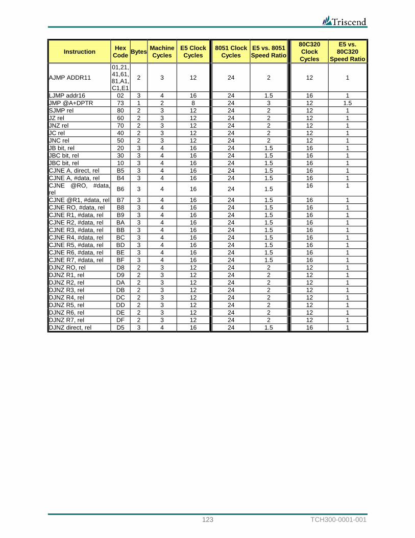
123 TCH300-0001-001
Instruction Hex Code Bytes Machine
Cycles E5 Clock Cycles
8051 Clock Cycles
E5 vs. 8051 Speed Ratio
80C320 Clock Cycles
E5 vs. 80C320
Speed Ratio
AJMP ADDR11 01,21, 41,61, 81,A1, C1,E1
2 3 12 24 2 12 1
LJMP addr16 02 3 4 16 24 1.5 16 1 JMP @A+DPTR 73 1 2 8 24 3 12 1.5 SJMP rel 80 2 3 12 24 2 12 1 JZ rel 60 2 3 12 24 2 12 1 JNZ rel 70 2 3 12 24 2 12 1 JC rel 40 2 3 12 24 2 12 1 JNC rel 50 2 3 12 24 2 12 1 JB bit, rel 20 3 4 16 24 1.5 16 1 JBC bit, rel 30 3 4 16 24 1.5 16 1 JBC bit, rel 10 3 4 16 24 1.5 16 1 CJNE A, direct, rel B5 3 4 16 24 1.5 16 1 CJNE A, #data, rel B4 3 4 16 24 1.5 16 1 CJNE @RO, #data, rel B6 3 4 16 24 1.5 16 1
CJNE @R1, #data, rel B7 3 4 16 24 1.5 16 1 CJNE RO, #data, rel B8 3 4 16 24 1.5 16 1 CJNE R1, #data, rel B9 3 4 16 24 1.5 16 1 CJNE R2, #data, rel BA 3 4 16 24 1.5 16 1 CJNE R3, #data, rel BB 3 4 16 24 1.5 16 1 CJNE R4, #data, rel BC 3 4 16 24 1.5 16 1 CJNE R5, #data, rel BD 3 4 16 24 1.5 16 1 CJNE R6, #data, rel BE 3 4 16 24 1.5 16 1 CJNE R7, #data, rel BF 3 4 16 24 1.5 16 1 DJNZ RO, rel D8 2 3 12 24 2 12 1 DJNZ R1, rel D9 2 3 12 24 2 12 1 DJNZ R2, rel DA 2 3 12 24 2 12 1 DJNZ R3, rel DB 2 3 12 24 2 12 1 DJNZ R4, rel DC 2 3 12 24 2 12 1 DJNZ R5, rel DD 2 3 12 24 2 12 1 DJNZ R6, rel DE 2 3 12 24 2 12 1 DJNZ R7, rel DF 2 3 12 24 2 12 1 DJNZ direct, rel D5 3 4 16 24 1.5 16 1
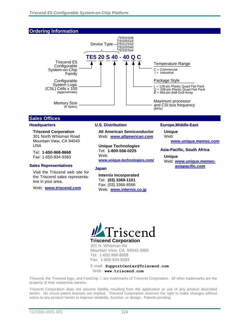
Triscend E5 Configurable System-on-Chip Platform
TCH300-0001-001 124
Ordering Information
TE5 20 S 40 - 40 Q CTriscend E5
ConfigurableSystem-on-Chip
Family
ConfigurableSystem Logic
(CSL) Cells x 100(approximate)
Memory Size(K bytes)
Temperature RangeC = Commercial I = Industrial
Package StyleL = 128-pin Plastic Quad Flat PackQ = 208-pin Plastic Quad Flat PackB = 484-pin Ball-Grid Array
Maximum processorand CSI bus frequency(MHz)
Device TypeTE502S08TE505S16TE512S32TE520S40TE532S64
Sales Offices HHeeaaddqquuaarrtteerrss
Triscend Corporation 301 North Whisman Road Mountain View, CA 94043 USA
Tel: 1-650-968-8668 Fax: 1-650-934-9393
SSaalleess RReepprreesseennttaattiivveess
Visit the Triscend web site for the Triscend sales representa-tive in your area. Web: www.triscend.com
UU..SS.. DDiissttrriibbuuttiioonn
All American Semiconductor Web: www.allamerican.com Unique Technologies Tel: 1-800-556-0225 Web: www.unique-technologies.com/
JJaappaann
Internix Incorporated Tel: (03) 3369-1101 Fax: (03) 3366-8566 Web: www.internix.co.jp
EEuurrooppee,,MMiiddddllee--EEaasstt
Unique Web: www.unique.memec.com
AAssiiaa--PPaacciiffiicc,, SSoouutthh AAffrriiccaa
Unique Web: www.unique.memec-
asiapacific.com
Triscend Corporation
301 N. Whisman Rd. Mountain View, CA 94043-3969 Tel: 1-650-968-8668 Fax: 1-650-934-9393 E-mail: [email protected] Web: www.triscend.com
Triscend, the Triscend logo, and FastChip are trademarks of Triscend Corporation. All other trademarks are the property of their respective owners.
Triscend Corporation does not assume liability resulting from the application or use of any product described herein. No circuit patent licenses are implied. Triscend Corporation reserves the right to make changes without notice to any product herein to improve reliability, function, or design. Patents pending.
®
TTrriisscceenndd EE55 CCoonnffiigguurraabbllee SSyysstteemm--oonn--CChhiipp FFaammiillyy
C O N T E N T S
OVERVIEW .............................................................3
ACCELERATED 8051 MICROCONTROLLER...............5 Programmable I/O Ports.....................................5 UART..................................................................5 Timers.................................................................5 Interrupts.............................................................6 Power Management............................................6 Power-On reset...................................................6
DMA CONTROLLER................................................6 Functional Description ........................................7 DMA Initialization and Termination .....................7 Transfer Modes ..................................................7 Bus Address Generation ....................................8 Data FIFO...........................................................8 CRC Feature.......................................................8 Interrupts Generation..........................................8 Configuration Registers ......................................9 Interfacing CSL Peripherals to the DMA Controller ..........................................................12
CONFIGURABLE SYSTEM INTERCONNECT (CSI) BUS15 Data Read Bus .................................................15 Data Write Bus .................................................15 Address Bus .....................................................15 Address Selectors ............................................16 Address Selector Operation .............................16 Address Specification .......................................17 Address Selector Modes ..................................17 Wait-State Monitor and Control Signals ...........18 Breakpoint Event Monitor and Control Signals .19 CSI Bus Transactions.......................................19 Side-band Signals.............................................20
CONFIGURABLE SYSTEM LOGIC (CSL) .................22 Bank Resources ...............................................23 CSL Cell Capabilities ........................................26 Logic Functions.................................................26 Arithmetic Functions .........................................26 Memory Functions ............................................28 Sequential Functions ........................................29
PROGRAMMABLE INPUT/OUTPUT (PIO) PINS ........ 30 Creating a PIO Port for the Microcontroller ...... 30 5-Volt Tolerant I/Os .......................................... 31 Storage Elements............................................. 31 PIO Input Side .................................................. 31 PIO Output Side ............................................... 32 Other PIO Options............................................ 32 Low-Power Mode ............................................. 32 JTAG Support .................................................. 33 Default, Unconfigured State ............................. 33 Default, Configured State................................. 33 Electro-static Discharge (ESD) Protection ....... 33
MEMORY INTERFACE UNIT.................................... 33 Functional Description...................................... 34 Initialization of the MIU ..................................... 35 MIU Register Description ................................. 35
ADDRESS MAPPERS............................................. 37 Code mappers.................................................. 40 C1, C2 – Fully programmable code mappers ..40 Data mappers................................................... 41 SFR export mapper.......................................... 43 Default Values for Higher-Order Address Mappers ........................................................... 43
SYSTEM DEBUGGER ............................................ 44 On-Chip Debugging Support ............................ 44 Debugging Support System Requirements...... 45
CONFIGURATION REGISTER UNIT (CRU)............... 46
SYSTEM INITIALIZATION ........................................ 46 Parallel Mode ................................................... 47 Serial Initialization............................................. 47 JTAG Initialization ............................................ 48 Slave Mode ...................................................... 49 'Stealth' Mode................................................... 49 Size of Initialization Data .................................. 50 Time to Initialize an E5 CSoC Device .............. 50 VSYS Control ................................................... 50
Triscend E5 Configurable System-on-Chip Platform
ii
CLOCKING AND GLOBAL SIGNAL DISTRIBUTION.....51 System clock select (BCLK) .............................51 Six Global Buffers.............................................52 Clock and Global Signal Stopping ....................52
ACCELERATED 8051 MICROCONTROLLER ARCHITECTURE ....................................................52
ALU...................................................................52 Accumulator......................................................52 B Register .........................................................52 Program Status Word.......................................53 Data Pointers ....................................................53 Scratch-pad RAM .............................................53 Stack Pointer ....................................................53 Timers/Counters ...............................................53 Memory Organization .......................................53 Special Function Registers ...............................55
INSTRUCTION SET.................................................62 Addressing Modes............................................62 Immediate Addressing......................................63
INTERRUPTS.........................................................64 Interrupt Sources ..............................................64 Priority Level Structure .....................................64 External Interrupts ............................................66 Response Time ................................................66
RESET CONDITIONS..............................................67 Power-On Reset (POR)....................................67 RST- Device Pin ...............................................67 JTAG Reset ......................................................68 Application Reset via RSTC Sideband Signal ..68 Watchdog Timer Reset.....................................68 System Behavior after a Reset Event...............68 Microcontroller Reset State ..............................68
POWER MANAGEMENT..........................................69 Power Management..........................................69 Power Saving....................................................69 Shutting Down the Crystal Oscillator ................70 Restarting the Crystal Oscillator after Exiting Power-Down Mode ...........................................70 Exiting Power-Down Mode ...............................71
GLOSSARY...........................................................72
LIFE SUPPORT POLICY .........................................72
PIN DESCRIPTION................................................. 74
PINOUT DIAGRAMS AND TABLES........................... 76 Available Packages and Package Codes ........ 76 Footprint-Compatibility ..................................... 76 Available PIOs by Package .............................. 76 128-pin Thin PQFP Footprint, top view ............ 77 128-pin Thin PQFP Package Pinout Tables .... 78 128-pin Thin PQFP Package Pins by Type...... 79 128-pin Thin PQFP Package Mechanical Drawing ............................................................ 80 208-pin PQFP Package Footprint, top view ..... 81 208-pin PQFP Package Pinout Tables ............ 82 208-pin PQFP Package Pins by Type.............. 83 208-pin PQFP Package Mechanical Drawing ..84 128-pin and 208-pin PQFP Package Land Pattern Dimensions.......................................... 85 484-ball BGA Package Footprint, top view through top of package .................................... 86 484-ball BGA Package Pinout Tables.............. 87 484-ball BGA Package Balls by Type .............. 89 484-ball BGA Package Mechanical Drawing.... 90
ELECTRICAL AND TIMING CHARACTERISTICS ......... 91 Absolute Maximum Ratings ............................. 91 Recommended Operating Conditions/DC Characteristics ................................................. 91
TRISCEND E5 SWITCHING CHARACTERISTIC GUIDELINES......................................................... 92
General E5 Timing Characteristics .................. 92 JTAG Interface Timing Characteristics ............ 92 Pin-to-Pin Guaranteed Timing Specifications ..93 Memory Interface Unit (MIU) Timing Characteristics ................................................. 96 Asynchronous Memory Interface Timing.......... 99 Configurable System Interconnect (CSI) Socket Timing Guidelines .......................................... 100 Sideband Signal Timing Characteristics ........ 104 Configurable System Logic (CSL) Cell (Combinatorial Logic Mode, Sequential Mode)105 Configurable System Logic (CSL) Cell (Arithmetic Mode)........................................... 107 Configurable System Logic (CSL) Cell (Memory Mode, Single-Port RAM) ................................ 108 Configurable System Logic (CSL) Cell (Memory Mode, Dual-Port RAM) ................................... 110 Configurable System Logic (CSL) Cell (Memory Mode, 8-bit Shift Register).............................. 111 Bus Clock and Global Buffers ........................ 112 Programmable Input/Output (PIO) Timing Guidelines ...................................................... 113
iii
TRISCEND E5 POWER/CURRENT CONSUMPTION CHARACTERISTICS .............................................115
Typical Power-Down Current Consumption (3.3 volts, room temperature) .........................115 Worst-Case Power-Down Current Consumption Characteristics..........................115 Typical Dynamic Power Consumption Component Estimates ....................................116
OUTPUT BUFFER SWITCHING CHARACTERISTICS .118
APPENDIX A: E5 INSTRUCTION TIMING...............119
ORDERING INFORMATION ................................... 124
SALES OFFICES ................................................. 124 Headquarters.................................................. 124 Sales Representatives ................................... 124 U.S. Distribution ............................................. 124 Japan.............................................................. 124 Europe,Middle-East........................................ 124 Asia-Pacific, South Africa............................... 124


![MPC8548E Configurable Development System … Configurable Development System Reference Manual, ... [4:0] ... MPC8548E Configurable Development System Reference Manual,](https://img.pdfslide.net/doc/110x75/5af028337f8b9ac62b8e4c0e/mpc8548e-configurable-development-system-configurable-development-system-reference.jpg)