Embed Size (px)
Citation preview
®
Tsi721™ Datasheet
April 4, 2016
Titl
Tsi721 Datasheet 2 April 4, 2016Integrated Device Technology
Table of ContentsAbout this Document......................................................................................................................6
Overview.................................................................................................................................................................................................... 6Document Conventions.............................................................................................................................................................................. 6Revision History ......................................................................................................................................................................................... 7
1. Device Overview............................................................................................................................ 81.1 Overview.................................................................................................................................................................................................... 81.2 Features..................................................................................................................................................................................................... 8
1.2.1 PCIe Features ............................................................................................................................................................................ 81.2.2 S-RIO Features .......................................................................................................................................................................... 91.2.3 Bridging Features ....................................................................................................................................................................... 91.2.4 Messaging Features ................................................................................................................................................................. 101.2.5 Block DMA Engine Features .................................................................................................................................................... 101.2.6 Miscellaneous Features.............................................................................................................................................................11
1.3 Block Diagram.......................................................................................................................................................................................... 121.3.1 PCIe Interface........................................................................................................................................................................... 121.3.2 S-RIO Interface......................................................................................................................................................................... 121.3.3 Messaging Engine .................................................................................................................................................................... 121.3.4 Mapping Engine........................................................................................................................................................................ 121.3.5 Block DMA Engine.................................................................................................................................................................... 12
1.4 Typical Applications ................................................................................................................................................................................. 131.4.1 Defense/Aerospace Application ............................................................................................................................................... 131.4.2 Video and Imaging Application ................................................................................................................................................. 151.4.3 Wireless Application ................................................................................................................................................................. 15
2. Signals ......................................................................................................................................... 172.1 Overview.................................................................................................................................................................................................. 172.2 Ballmap.................................................................................................................................................................................................... 182.3 Pinlist ....................................................................................................................................................................................................... 192.4 PCIe Signals ............................................................................................................................................................................................ 192.5 S-RIO Signals .......................................................................................................................................................................................... 202.6 General Signals ....................................................................................................................................................................................... 202.7 I2C Signals .............................................................................................................................................................................................. 212.8 JTAG and Test Interface Signals.............................................................................................................................................................. 212.9 GPIO Signals ........................................................................................................................................................................................... 222.10 Power-up Signals..................................................................................................................................................................................... 232.11 Power Supply Signals .............................................................................................................................................................................. 26
3. Electrical Characteristics ........................................................................................................... 273.1 Absolute Maximum Ratings ..................................................................................................................................................................... 273.2 Recommended Operating Conditions...................................................................................................................................................... 283.3 Power Consumption................................................................................................................................................................................. 28
Co
Tsi721 Datasheet 3 April 4, 2016Integrated Device Technology
3.4 Power Supply Sequencing....................................................................................................................................................................... 293.4.1 Power-Up Sequencing.............................................................................................................................................................. 293.4.2 Power-Down Sequencing ......................................................................................................................................................... 29
3.5 DC Operating Characteristics .................................................................................................................................................................. 303.6 Decoupling Recommendation.................................................................................................................................................................. 313.7 AC Timing Specifications ......................................................................................................................................................................... 31
3.7.1 PCIe Differential Receiver Specifications ................................................................................................................................. 313.7.2 PCIe Differential Transmitter Specifications ............................................................................................................................. 343.7.3 RapidIO SerDes Characteristics............................................................................................................................................... 383.7.4 Level I Long Run Transmitter Specifications ............................................................................................................................ 433.7.5 Reference Clocks – PCCLKP/N and REFCLKP/N................................................................................................................... 573.7.6 JTAG and Test Interface Signal Timings .................................................................................................................................. 593.7.7 I2C Interface Signal Timings .................................................................................................................................................... 603.7.8 GPIO Interface Signal Timings ................................................................................................................................................. 613.7.9 RSTn Signal Timings................................................................................................................................................................ 61
4. Package Specifications............................................................................................................... 624.1 Package Dimensions ............................................................................................................................................................................... 624.2 Package Diagrams................................................................................................................................................................................... 634.3 Thermal Characteristics ........................................................................................................................................................................... 644.4 Moisture Sensitivity .................................................................................................................................................................................. 64
5. Ordering Information................................................................................................................... 65
Tsi721 Datasheet 4 April 4, 2016Integrated Device Technology
List of FiguresFigure 1: Block Diagram............................................................................................................................................................................................. 12Figure 2: Defense/Aerospace Application ................................................................................................................................................................ 14Figure 3: Video and Imaging Application ................................................................................................................................................................. 15Figure 4: Wireless Application .................................................................................................................................................................................. 16Figure 5: Ballmap ....................................................................................................................................................................................................... 18Figure 6: S-RIO Definition of Transmitter Amplitude and Swing ................................................................................................................................ 39Figure 7: S-RIO Transition Symbol Transmit Eye Mask............................................................................................................................................. 44Figure 8: S-RIO Single Frequency Sinusoidal Jitter Limits ........................................................................................................................................ 46Figure 9: S-RIO Level I Receiver Input Mask............................................................................................................................................................. 47Figure 10: Transition and Steady State Symbol Eye Mask .......................................................................................................................................... 51Figure 11: Level II Receiver Input Compliance Mask................................................................................................................................................... 56Figure 12: HCSL to REFCLKP/N / PCCLKP/N ............................................................................................................................................................ 58Figure 13: LVDS to REFCLKP/N / PCCLKP/N............................................................................................................................................................. 58Figure 14: LVPECL to REFCLKP/N / PCCLKP/N ........................................................................................................................................................ 58Figure 15: LVPECL to REFCLKP/N / PCCLKP/N ........................................................................................................................................................ 59Figure 16: I2C Interface Signal Timings....................................................................................................................................................................... 60Figure 17: Package Diagrams...................................................................................................................................................................................... 63
Tsi721 Datasheet 5 April 4, 2016Integrated Device Technology
List of TablesTable 1: Signal Types ............................................................................................................................................................................................... 17Table 2: PCIe Signals ............................................................................................................................................................................................... 19Table 3: S-RIO Signals ............................................................................................................................................................................................. 20Table 4: General Signals .......................................................................................................................................................................................... 20Table 5: I2C Signals.................................................................................................................................................................................................. 21Table 6: JTAG Interface Signals ............................................................................................................................................................................... 21Table 7: GPIO Signals .............................................................................................................................................................................................. 22Table 8: GPIO Mapping to Power-up Signals ........................................................................................................................................................... 22Table 9: Power-Up Signals ....................................................................................................................................................................................... 23Table 10: Power Supply Signals ................................................................................................................................................................................. 26Table 11: Absolute Maximum Ratings ........................................................................................................................................................................ 27Table 12: Recommended Operating Conditions......................................................................................................................................................... 28Table 13: Power Consumption.................................................................................................................................................................................... 28Table 14: Power Supply Sequencing Ramp Times .................................................................................................................................................... 29Table 15: 3.3V LVTTL DC Operating Characteristics at Recommended Operating Condition of 3.3V ...................................................................... 30Table 16: 2.5V LVTTL DC Operating Characteristics at Recommended Operating Condition of 2.5V ...................................................................... 30Table 17: Decoupling Recommendation..................................................................................................................................................................... 31Table 18: PCIe Differential Receiver Specifications ................................................................................................................................................... 31Table 19: PCIe Differential Transmitter Specifications................................................................................................................................................ 34Table 20: Level I Short Run Transmitter AC Timing Specifications ............................................................................................................................ 42Table 21: Level I Long Run Transmitter AC Timing Specifications............................................................................................................................. 43Table 22: Level I Near-End (Tx) Template Intervals ................................................................................................................................................... 44Table 23: Level I Receiver Electrical Input Specifications .......................................................................................................................................... 45Table 24: Level I Receiver Input Jitter Tolerance Specifications................................................................................................................................. 46Table 25: Level I Far-End (Rx) Template Intervals ..................................................................................................................................................... 47Table 26: Level II Short Run Transmitter Output Electrical Specifications.................................................................................................................. 49Table 27: Level II Medium Run Transmitter Output Electrical Specifications ............................................................................................................. 50Table 28: Level II Medium Run Near-End (Tx) Template Intervals ............................................................................................................................. 52Table 29: Level II Short Run Receiver Electrical Input Specifications ........................................................................................................................ 53Table 30: Level II MR Receiver Electrical Input Specifications................................................................................................................................... 55Table 31: Level II Far-End (Rx) Template Intervals .................................................................................................................................................... 56Table 32: PCCLKP/N and REFCLKP/NClock Electrical Characteristics .................................................................................................................... 57Table 33: JTAG and Test Interface AC Specifications ................................................................................................................................................ 59Table 34: I2C Interface AC Specifications .................................................................................................................................................................. 60Table 35: GPIO Interface AC Specifications............................................................................................................................................................... 61Table 36: RSTn Signal AC Specifications................................................................................................................................................................... 61Table 37: Package Dimensions .................................................................................................................................................................................. 62Table 38: Junction to Ambient Characteristics – Theta JB/JC.................................................................................................................................... 64Table 39: Junction to Ambient Characteristics – Theta JA ......................................................................................................................................... 64
Tsi721 Datasheet 6 April 4, 2016Integrated Device Technology
About this DocumentTopics discussed include the following:
• Overview
• Document Conventions
• Revision History
OverviewThe Tsi721 Datasheet provides signal, electrical, and packaging information about the Tsi721. It is intended for hardware engineers who are designing system interconnect applications with the device.
Document ConventionsThis document uses the following conventions.
Non-differential Signal Notation
Non-differential signals are either active-low or active-high. An active-low signal has an active state of logic 0 (or the lower voltage level), and is denoted by a lowercase “n”. An active-high signal has an active state of logic 1 (or the higher voltage level), and is not denoted by a special character. The following table illustrates the non-differential signal naming convention.
Differential Signal Notation
Differential signals consist of pairs of complement positive and negative signals that are measured at the same time to determine a signal’s active or inactive state (they are denoted by “_p” and “_n”, respectively). The following table illustrates the differential signal naming convention.
State Single-line signal Multi-line signal
Active low NAMEn NAMEn[3]
Active high NAME NAME[3]
State Single-line signal Multi-line signal
Inactive NAME_p = 0NAME_n = 1
NAME_p[3] = 0NAME_n[3] = 1
Active NAME_p = 1NAME_n = 0
NAME_p[3] is 1NAME_n[3] is 0
Tsi721 Datasheet 7 April 4, 2016Integrated Device Technology
Object Size Notation• A byte is an 8-bit object.
• A PCIe word is a 16-bit object.
• A PCIe doubleword (DW) is a 32-bit object.
• An S-RIO word is a 32-bit object.
• An S-RIO doubleword (Dword) is a 64-bit object.
Numeric Notation• Hexadecimal numbers are denoted by the prefix 0x (for example, 0x04).
• Binary numbers are denoted by the prefix 0b (for example, 0b010).
• Registers that have multiple iterations are denoted by {x..y} in their names; where x is first register and address, and y is the last register and address. For example, REG{0..1} indicates there are two versions of the register at different addresses: REG0 and REG1.
Symbols
Revision HistoryApril 4, 2016• Added GCLV, GILH, and GILV part numbers to Ordering Information
May 5, 2014• Updated the description of the VIN_DIFF parameter in Table 32
December 3, 2012• Updated Ordering Information with production ordering numbers
February 28, 2012• Added a footnote to Absolute Maximum Ratings, and removed the minimum rating for TJN from the same section
• Added TJN and a footnote to Recommended Operating Conditions
December 16, 2011• Updated the minimum and maximum values for AVDD10 in Recommended Operating Conditions
• Added Power Consumption data
• Changed the Moisture Sensitivity Level to 4
This symbol indicates important configuration information or suggestions.
This symbol indicates procedures or operating levels that may result in misuse or damage to the device.
Tsi721 Datasheet 8 April 4, 2016Integrated Device Technology
1. Device OverviewTopics discussed include the following:
• Overview
• Features
• Block Diagram
• Typical Applications
1.1 OverviewIDT is the leading supplier of RapidIO® and PCI Express Interconnect solutions, providing a broad portfolio of switches, bridges, IP, and development platforms for defense aerospace, video, imaging, and wireless markets. The Tsi721 is IDT's solution for hardware-based PCIe Gen2 to RapidIO Gen2 protocol conversion in a bridging device.
The Tsi721 converts transactions from PCIe to RapidIO, and vice versa, and provides full line rate bridging at 20 Gbaud. Using the Tsi721, designers can develop heterogeneous systems that leverage the peer-to-peer networking performance of RapidIO while using multiprocessor clusters that may be only PCIe enabled. In addition, applications that require large amounts of data transferred efficiently without processor involvement can be executed using the full line rate of the Tsi721’s Block DMA Engine and Messaging Engine.
Key to the Tsi721 is the hardware bridging functionality that converts PCIe transactions to RapidIO, and vice versa. The Tsi721 supports PCIe non-transparent bridging for transaction mapping. The device has both RapidIO and PCIe endpoints embedded in the bridge, and each of its Block DMA/Messaging DMA channels can buffer up to 8 KB of data on the PCIe side.
1.2 FeaturesThe Tsi721 supports the following features.
1.2.1 PCIe Features
• PCIe 2.1 standard compliant
• 5/2.5 Gbaud link speed
• x4/x2/x1 link width
• 128- and 256-byte maximum payload
• Advanced error reporting
• Internal error reporting
• Lane reversal
• Automatic polarity inversion
• Dynamic port width: x4 drops to x1
• ECRC support
• INTx, MSI, and MSI-X support
Tsi721 Datasheet 9 April 4, 2016Integrated Device Technology
• Single virtual channel, VC0
• Single traffic class, TC0
— Generates only PCIe posted/non-posted TLPs with TC0
— Generates only PCIe Cpl/CplD TLPs with TC matching their requests
— Accepts PCIe TLPs with any TC
• Four BARs
— Prefetchable BAR with 32- or 64-bit addressing for PCIe-to-S-RIO bridging
— Non-prefetchable BAR with 32- or 64-bit addressing for PCIe-to-S-RIO bridging
— Non-prefetchable BAR with 32-bit addressing for PCIe MWr to S-RIO doorbell bridging
— Non-prefetchable BAR with 32-bit addressing for Tsi721 internal register access
• Initial credit advertisement programmable through EEPROM
• Dynamic control of credits through registers
• Starvation prevention based on flow control credit updates
• Large buffers
— 12 KB/2 KB/12 KB input buffers for up to 127 posted/non-posted/completion TLPs
— 12 KB/2 KB/12 KB output buffers for up to 128 posted/non-posted/completion TLPs
• Debug features
— Slave analog loopback through a control register
— Slave loopback using TS1/TS2 ordered sets
— Master loopback
— Internal error reporting
— ECC protection on internal memories
1.2.2 S-RIO Features
• S-RIO 2.1 standard compliant
• 5/3.125/2.5/1.25 Gbaud link speed
• x4/x2/x1 link width
• 34-, 50-, and 66-bit addressing
• 16 destID filters
• 8 S-RIO flows
• 9-KB ingress buffer (32 x 288)
• 9-KB egress buffer (32 x 288)
• Lane reversal
• Lane polarity inversion
1.2.3 Bridging Features
• Store and forward from PCIe to S-RIO
• Store and forward from S-RIO to PCIe
• Line rate support for 64 byte and larger packets
• 32 outstanding PCIe requests to root complex
Tsi721 Datasheet 10 April 4, 2016Integrated Device Technology
• 32 outstanding S-RIO NREAD/maintenance read requests to S-RIO network
• 32 outstanding S-RIO NWRITE_R/maintenance write/doorbell requests to S-RIO network
• 12-KB completion reassembly buffer
• 8 windows from PCIe to S-RIO with 8 zones (sub windows) per window
• 8 windows from S-RIO to PCIe
• Initiates and receives the following S-RIO transactions:
— NREAD
— SWRITE/NWRITE/NWRITE_R
— Maintenance read and write
— Port-write
— Doorbell
— Type 8 response
— Type 13 response
• Initiates and receives the following PCIe transactions:
— MWr
— MRd
— Cpl
— CplD
• Round-robin scheduling between Mapping Engine, Block DMA Engine, and Messaging traffic to the S-RIO link
• Round-robin scheduling between Mapping Engine, Block DMA Engine, and Messaging traffic to the PCIe link
• Forward bridge
— Connects PCIe root complex to S-RIO network
— PCIe Type 0 configuration header
1.2.4 Messaging Features
• 8 Tx queues with one dedicated messaging DMA engine per Tx queue
• 8 Rx queues with one dedicated messaging DMA engine per Rx queue
• Descriptor prefetch per Tx queue
• 32 outstanding PCIe requests to root complex
• 8-KB message segment reassembly buffer per Tx queue
• Round-robin scheduling among Tx queues
• One outstanding message per Tx queue
• 16 receive contexts per Rx queue
1.2.5 Block DMA Engine Features
• 8 DMA channels
• Each DMA channel can perform DMA writes from root complex to S-RIO network, or DMA reads from S-RIO network to root complex
— DMA from PCIe port to PCIe port is not supported
— DMA from S-RIO port to S-RIO port is not supported
Tsi721 Datasheet 11 April 4, 2016Integrated Device Technology
• Round-robin scheduling among DMA channels
• DMA descriptors for all channels reside on PCIe side
• Scatter-and-gather with descriptor list
• Supports DMA strides
• Supports up to 64 MB data for a single descriptor
• Supports both read and write descriptors per DMA channel
• Dynamic descriptor chaining
• Flexible addressing modes
— Linear addressing
— Constant addressing
• Descriptor prefetch
• 32 outstanding PCIe requests to root complex
• 64 outstanding S-RIO NREAD/maintenance read requests to S-RIO network
• 64 outstanding S-RIO NWRITE_R/maintenance write requests to S-RIO network
• Supports the following S-RIO transactions:
— NREAD
— NWRITE
— SWRITE
— NWRITE_R
— Maintenance read
— Maintenance write
1.2.6 Miscellaneous Features
• I2C interface supports the following:
— As a slave, being read/written by an external master during normal operations
— As a master, reading external EEPROM during boot load
— As a master, reading/writing other external devices during normal operations
• JTAG 1149.1, 1149.6 (AC JTAG)
• 16 GPIO pins
Tsi721 Datasheet 12 April 4, 2016Integrated Device Technology
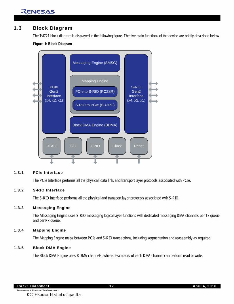
1.3 Block DiagramThe Tsi721 block diagram is displayed in the following figure. The five main functions of the device are briefly described below.
Figure 1: Block Diagram
1.3.1 PCIe Interface
The PCIe Interface performs all the physical, data link, and transport layer protocols associated with PCIe.
1.3.2 S-RIO Interface
The S-RIO Interface performs all the physical and transport layer protocols associated with S-RIO.
1.3.3 Messaging Engine
The Messaging Engine uses S-RIO messaging logical layer functions with dedicated messaging DMA channels per Tx queue and per Rx queue.
1.3.4 Mapping Engine
The Mapping Engine maps between PCIe and S-RIO transactions, including segmentation and reassembly as required.
1.3.5 Block DMA Engine
The Block DMA Engine uses 8 DMA channels, where descriptors of each DMA channel can perform read or write.
JTAG I2C GPIO Clock Reset
Block DMA Engine (BDMA)
Messaging Engine (SMSG)
PCIeGen2
Interface(x4, x2, x1)
S-RIO Gen2
Interface(x4, x2, x1)
Mapping Engine
PCIe to S-RIO (PC2SR)
S-RIO to PCIe (SR2PC)
Tsi721 Datasheet 13 April 4, 2016Integrated Device Technology
1.4 Typical ApplicationsThe Tsi721 supports the following typical applications:
• Defense and aerospace
— Radar
— Sonar
— Navigations systems
• Medical imaging
— CT scanners
— MRIs
• Video
— Teleconferencing
— Head end
• Wireless
— Baseband cards with x86
Three of Tsi721’s typical applications – defense/aerospace, video/imaging, and wireless – are discussed in the following sections.
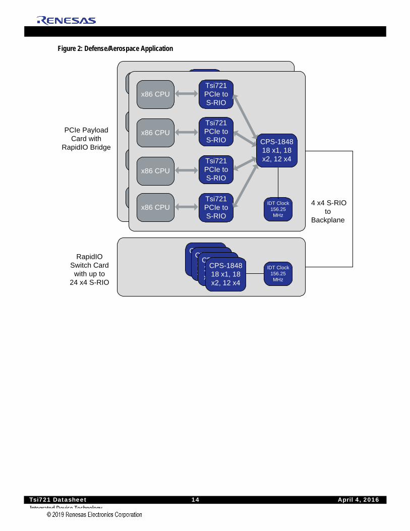
1.4.1 Defense/Aerospace Application
In defense applications, the Tsi721 supports the use of PCIe enabled x86 processors to RapidIO backplanes. This provides system designers with the best of both worlds: the floating point and MIPs horsepower of the latest generation of x86 solutions, with the superior peer-to-peer networking performance of RapidIO architectures.
By using the Tsi721 combined with IDT’s RapidIO Gen2 switches, payload processor cards with x86 processors can be used with existing RapidIO 1.3 backplanes operating at up to 3.125 Gbaud, or the same card can be used with RapidIO Gen2 compatible backplanes operating at 5 Gbaud.
Tsi721 Datasheet 14 April 4, 2016Integrated Device Technology
Figure 2: Defense/Aerospace Application
CPS-184818 x1, 18 x2, 12 x4
CPS-184818 x1, 18 x2, 12 x4
CPS-184818 x1, 18 x2, 12 x4
CPS-184818 x1, 18 x2, 12 x4
CPS-184818 x1, 18 x2, 12 x4
x86 CPUTsi721PCIe to SRIO
x86 CPUTsi721PCIe to SRIO
x86 CPUTsi721PCIe to SRIO
x86 CPUTsi721PCIe to SRIO
CPS-184818 x1, 18 x2, 12 x4
Tsi721PCIe to S-RIO
Tsi721PCIe to S-RIO
Tsi721PCIe to S-RIO
Tsi721PCIe to S-RIO
4 x4 S-RIO to
Backplane
PCIe Payload Card with
RapidIO Bridge
RapidIO Switch Card with up to
24 x4 S-RIO
x86 CPU
x86 CPU
x86 CPU
x86 CPUIDT Clock
156.25MHz
IDT Clock156.25 MHz
Tsi721 Datasheet 15 April 4, 2016Integrated Device Technology
1.4.2 Video and Imaging Application
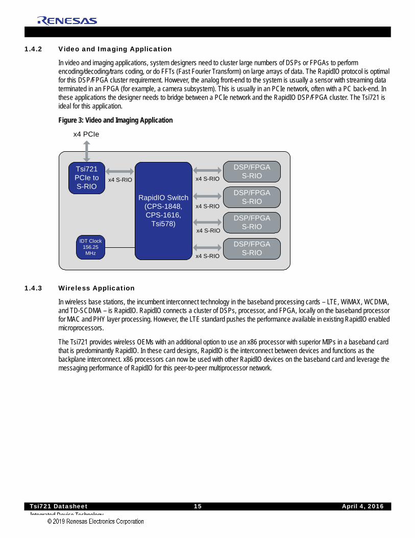
In video and imaging applications, system designers need to cluster large numbers of DSPs or FPGAs to perform encoding/decoding/trans coding, or do FFTs (Fast Fourier Transform) on large arrays of data. The RapidIO protocol is optimal for this DSP/FPGA cluster requirement. However, the analog front-end to the system is usually a sensor with streaming data terminated in an FPGA (for example, a camera subsystem). This is usually in an PCIe network, often with a PC back-end. In these applications the designer needs to bridge between a PCIe network and the RapidIO DSP/FPGA cluster. The Tsi721 is ideal for this application.
Figure 3: Video and Imaging Application
1.4.3 Wireless Application
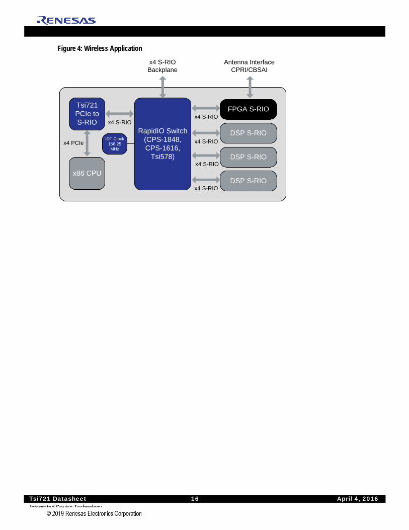
In wireless base stations, the incumbent interconnect technology in the baseband processing cards – LTE, WiMAX, WCDMA, and TD-SCDMA – is RapidIO. RapidIO connects a cluster of DSPs, processor, and FPGA, locally on the baseband processor for MAC and PHY layer processing. However, the LTE standard pushes the performance available in existing RapidIO enabled microprocessors.
The Tsi721 provides wireless OEMs with an additional option to use an x86 processor with superior MIPs in a baseband card that is predominantly RapidIO. In these card designs, RapidIO is the interconnect between devices and functions as the backplane interconnect. x86 processors can now be used with other RapidIO devices on the baseband card and leverage the messaging performance of RapidIO for this peer-to-peer multiprocessor network.
Tsi721PCIe to S-RIO
x4 PCIe
x4 S-RIO
DSP/FPGAS-RIOx4 S-RIO
x4 S-RIO
DSP/FPGAS-RIO
x4 S-RIO
DSP/FPGAS-RIO
x4 S-RIO
DSP/FPGAS-RIO
IDT Clock156.25MHz
RapidIO Switch(CPS-1848, CPS-1616,
Tsi578)
Tsi721 Datasheet 16 April 4, 2016Integrated Device Technology
Figure 4: Wireless Application
FPGA S-RIOTsi721PCIe to S-RIO
x4 PCIe
RapidIO Switch(CPS-1848, CPS-1616,
Tsi578)
DSP S-RIO
DSP S-RIO
DSP S-RIOx4 S-RIO
x4 S-RIO
x4 S-RIO
x4 S-RIOx4 S-RIO
x86 CPU
x4 S-RIO Backplane
Antenna Interface CPRI/CBSAI
IDT Clock156.25 MHz
Tsi721 Datasheet 17 April 4, 2016Integrated Device Technology
2. SignalsTopics discussed include the following:
• Overview
• Ballmap
• Pinlist
• PCIe Signals
• S-RIO Signals
• General Signals
• I2C Signals
• JTAG and Test Interface Signals
• GPIO Signals
• Power-up Signals
• Power Supply Signals
2.1 OverviewThe following conventions are used in this chapter:
• Signals with the suffix “P” are the positive half of a differential pair.
• Signals with the suffix “N” are the negative half of a differential pair.
• Signals with the suffix “n” are active low.
Signals are classified according to the types defined in the following table.
Table 1: Signal Types
Pin Type Definition
I 3.3/2.5V LVTTL Input
O 3.3/2.5V LVTTL Output
IO 3.3/2.5V LVTTL Bidirectional
IO-OD 3.3/2.5V LVTTL Bidirectional Open Drain
OD 3.3/2.5V LVTTL Open Drain
I-PU 3.3/2.5V LVTTL Input with Pull-up
I-PD 3.3/2.5V LVTTL Input with Pull-down
Tsi721 Datasheet 18 April 4, 2016Integrated Device Technology
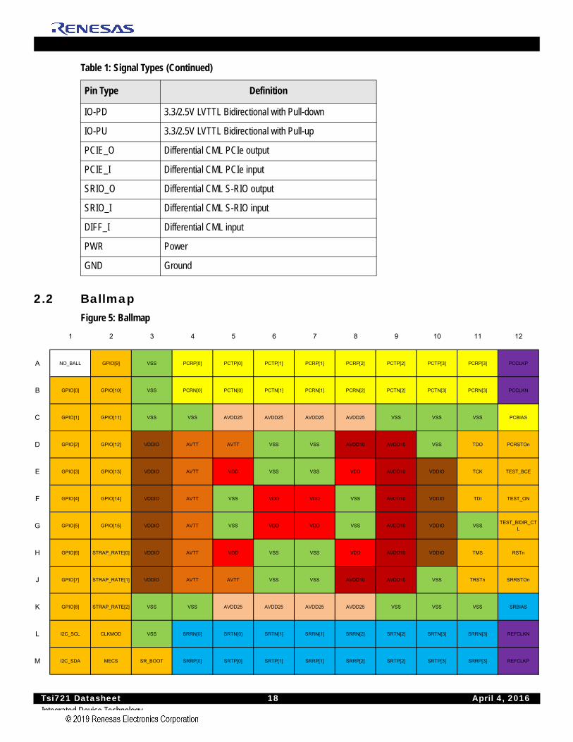
2.2 BallmapFigure 5: Ballmap
IO-PD 3.3/2.5V LVTTL Bidirectional with Pull-down
IO-PU 3.3/2.5V LVTTL Bidirectional with Pull-up
PCIE_O Differential CML PCIe output
PCIE_I Differential CML PCIe input
SRIO_O Differential CML S-RIO output
SRIO_I Differential CML S-RIO input
DIFF_I Differential CML input
PWR Power
GND Ground
Table 1: Signal Types (Continued)
Pin Type Definition
1 2 3 4 5 6 7 8 9 10 11 12
A NO_BALL GPIO[9] VSS PCRP[0] PCTP[0] PCTP[1] PCRP[1] PCRP[2] PCTP[2] PCTP[3] PCRP[3] PCCLKP
B GPIO[0] GPIO[10] VSS PCRN[0] PCTN[0] PCTN[1] PCRN[1] PCRN[2] PCTN[2] PCTN[3] PCRN[3] PCCLKN
C GPIO[1] GPIO[11] VSS VSS AVDD25 AVDD25 AVDD25 AVDD25 VSS VSS VSS PCBIAS
D GPIO[2] GPIO[12] VDDIO AVTT AVTT VSS VSS AVDD10 AVDD10 VSS TDO PCRSTOn
E GPIO[3] GPIO[13] VDDIO AVTT VDD VSS VSS VDD AVDD10 VDDIO TCK TEST_BCE
F GPIO[4] GPIO[14] VDDIO AVTT VSS VDD VDD VSS AVDD10 VDDIO TDI TEST_ON
G GPIO[5] GPIO[15] VDDIO AVTT VSS VDD VDD VSS AVDD10 VDDIO VSSTEST_BIDIR_CT
L
H GPIO[6] STRAP_RATE[0] VDDIO AVTT VDD VSS VSS VDD AVDD10 VDDIO TMS RSTn
J GPIO[7] STRAP_RATE[1] VDDIO AVTT AVTT VSS VSS AVDD10 AVDD10 VSS TRSTn SRRSTOn
K GPIO[8] STRAP_RATE[2] VSS VSS AVDD25 AVDD25 AVDD25 AVDD25 VSS VSS VSS SRBIAS
L I2C_SCL CLKMOD VSS SRRN[0] SRTN[0] SRTN[1] SRRN[1] SRRN[2] SRTN[2] SRTN[3] SRRN[3] REFCLKN
M I2C_SDA MECS SR_BOOT SRRP[0] SRTP[0] SRTP[1] SRRP[1] SRRP[2] SRTP[2] SRTP[3] SRRP[3] REFCLKP
Tsi721 Datasheet 19 April 4, 2016Integrated Device Technology
2.3 PinlistFor a list-based version of Tsi721’s pin to signal mapping, see the Tsi721 Ballmap and Pinlist.
2.4 PCIe Signals
Table 2: PCIe Signals
Name Pin Type Description
PCTP[3:0]
PCTN[3:0]
PCIE_O Differential transmit data for the PCIe port.
PCRP[3:0]
PCRN[3:0]
PCIE_I Differential receive data for the PCIe port.
PCCLKP
PCCLKN
DIFF_I PCIe reference clock input.
When in PCIe common clock mode (CLKMOD pin is high, see the “Clocking” chapter in the Tsi721 User Manual), PCCLKP/N requires a clock frequency of 100 MHz.
When in PCIe non-common clock mode (CLKMOD pin is low), PCCLKP/N requires a clock frequency as selected by CLKSEL[1:0], and must have the same clock frequency as REFCLKP/N.
PCRSTOn IO It is an output for normal operation and an input during scan test mode.
As an asynchronous active-low reset output, this pin is low when the following occurs: • The PCIe port detects hot reset• The PCIe port is DL_DOWN
Tsi721 Datasheet 20 April 4, 2016Integrated Device Technology
2.5 S-RIO Signals
2.6 General Signals
Table 3: S-RIO Signals
Name Pin Type Descriptiona
a. For information on S-RIO signals that are used for power-up purposes only, see Power-up Signals.
SRTP[3:0]
SRTN[3:0]
SRIO_O Differential transmit data for the S-RIO port.
SRRP[3:0]
SRRN[3:0]
SRIO_I Differential receive data for the S-RIO port.
SRRSTOn IO It is an output for normal operation and an input during scan test mode.
As an asynchronous active-low reset output, this pin is low when four consecutive S-RIO reset symbols are received, and SELF_RST is set to 1 in the RapidIO PLM Port Implementation Specific Control Register
MECS IO-PD Asynchronous S-RIO Multicast Event Control Symbol (MECS). Its direction is controlled by the MECS_O bit in the Device Control Register.
As an input, a rising or falling edge triggers an S-RIO MECS to be sent on the S-RIO link. Use the RIO_PLM_SP0_MECS_FWD.SUBSCRIPTION/MULT_CS and RIO_EM_MECS_TRIG_EN.CMD_EN to select the CMD field that should be set with the MECS. Multiple MECSs with different CMD fields can be generated by setting these fields appropriately.
As an output, this signal is toggled when an S-RIO MECS is received. Only a single MECS CMD value should be selected to toggle the MECS input. Set the RIO_EM_MECS_CAP_EN.CMD_EN to select the CMD value to be propagated to the MECS pin. Note: Only 1 bit should be enabled in CMD_EN.
Table 4: General Signals
Name Pin Type Description
RSTn I-PU Fundamental reset (device reset).Assertion of this signal resets all logic inside the Tsi721.
REFCLKP
REFCLKN
DIFF_I S-RIO reference clock input. REFCLK requires a clock frequency as selected by CLKSEL[1:0].
Tsi721 Datasheet 21 April 4, 2016Integrated Device Technology
2.7 I2C SignalsThe I2C Interface is used for the following:
• As a master, downloading configuration from EEPROM
• As a master, allowing the PCIe root complex or the S-RIO host to configure other I2C expansion devices
• As a slave, exposing internal register space to an I2C master (Note: To be used for lab debug or another master-driven initialization).
2.8 JTAG and Test Interface Signals
Table 5: I2C Signals
Name Pin Type Descriptiona
a. For information on I2C signals that are used for power-up purposes only, see Power-up Signals.
I2C_SCL IO-OD Serial clock for the I2C Interface with a maximum frequency of 100 kHz.
I2C_SDA IO-OD Serial data for the I2C Interface.
Table 6: JTAG Interface Signals
Name Pin Type Description
TCK I-PD IEEE 1149.1/1149.6 test access port. Clock input.
TDI I-PU IEEE 1149.1/1149.6 test access port. Serial data input
TDO O IEEE 1149.1/1149.6 test access port. Serial data output
TMS I-PU IEEE 1149.1/1149.6 test access port. Test mode select
TRSTn I-PU IEEE 1149.1/1149.6 test access port. Reset input.
This input must be asserted during the assertion of RSTn. Thereafter, it can be left in either state.
TEST_ON I-PD Test mode pin. Tie low or NC for normal operation.
TEST_BCE I-PU Boundary scan compatibility enabled pin. This input aids 1149.6 testing. It must be tied to VDDIO (or NC as there is internal pull up in pad) during normal operation of the device.
0 = JTAG chain includes SerDes registers. SerDes registers are accessible to external JTAG pins. Used during ATE and lab debug of SerDes registers through an external JTAG Controller.
1 = JTAG chain does not include SerDes registers. SerDes register are accessible through the internal register bus for BAR 0 access.
TEST_BIDIR_CTL I-PU Test mode pin. Tie high or NC for normal operation.
Tsi721 Datasheet 22 April 4, 2016Integrated Device Technology
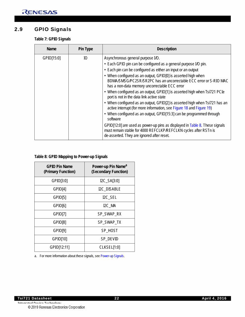
2.9 GPIO Signals
Table 7: GPIO Signals
Name Pin Type Description
GPIO[15:0] IO Asynchronous general purpose I/O. • Each GPIO pin can be configured as a general purpose I/O pin. • Each pin can be configured as either an input or an output• When configured as an output, GPIO[0] is asserted high when
BDMA/SMSG/PC2SR/SR2PC has an uncorrectable ECC error or S-RIO MAC has a non-data memory uncorrectable ECC error
• When configured as an output, GPIO[1] is asserted high when Tsi721 PCIe port is not in the data link active state
• When configured as an output, GPIO[2] is asserted high when Tsi721 has an active interrupt (for more information, see Figure 18 and Figure 19)
• When configured as an output, GPIO[15:3] can be programmed through software
GPIO[12:0] are used as power-up pins as displayed in Table 8. These signals must remain stable for 4000 REFCLKP/REFCLKN cycles after RSTn is de-asserted. They are ignored after reset.
Table 8: GPIO Mapping to Power-up Signals
GPIO Pin Name(Primary Function)
Power-up Pin Namea (Secondary Function)
a. For more information about these signals, see Power-up Signals.
GPIO[3:0] I2C_SA[3:0]
GPIO[4] I2C_DISABLE
GPIO[5] I2C_SEL
GPIO[6] I2C_MA
GPIO[7] SP_SWAP_RX
GPIO[8] SP_SWAP_TX
GPIO[9] SP_HOST
GPIO[10] SP_DEVID
GPIO[12:11] CLKSEL[1:0]
Tsi721 Datasheet 23 April 4, 2016Integrated Device Technology
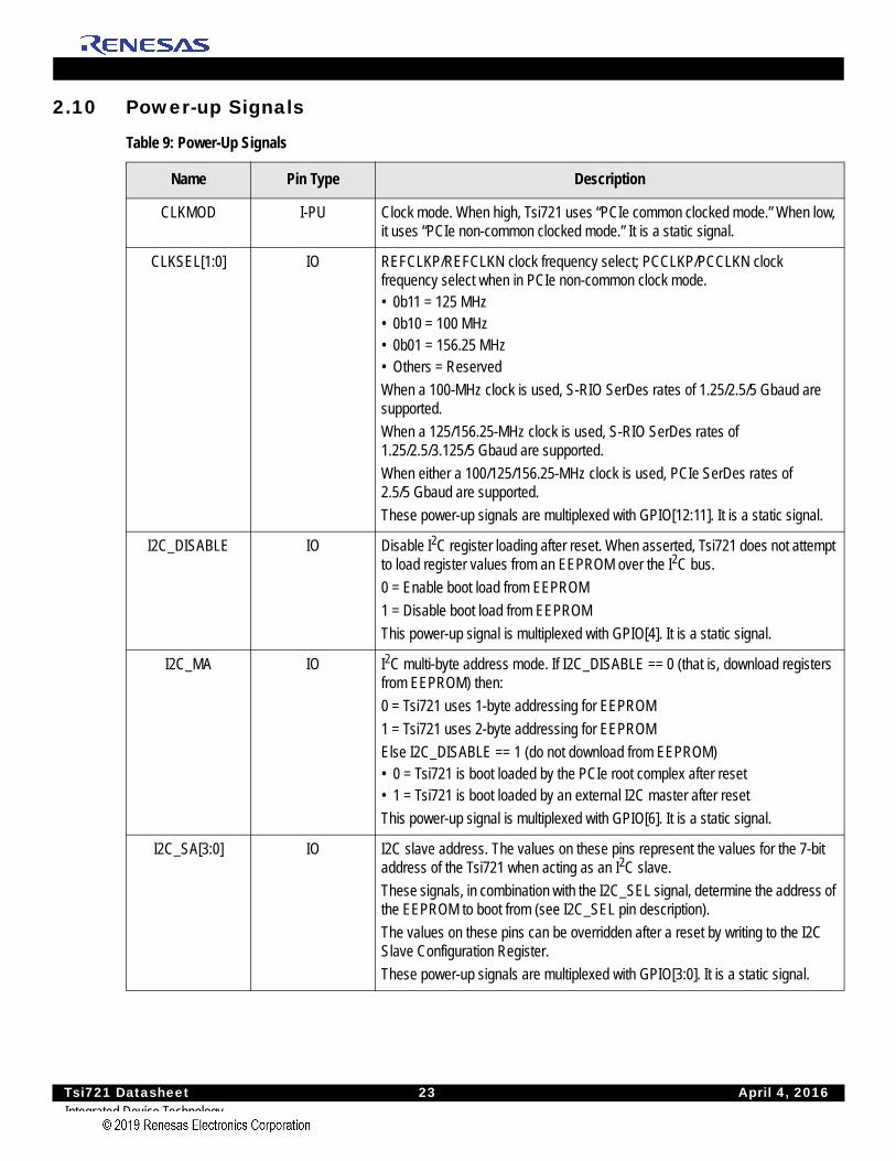
2.10 Power-up Signals
Table 9: Power-Up Signals
Name Pin Type Description
CLKMOD I-PU Clock mode. When high, Tsi721 uses “PCIe common clocked mode.” When low, it uses “PCIe non-common clocked mode.” It is a static signal.
CLKSEL[1:0] IO REFCLKP/REFCLKN clock frequency select; PCCLKP/PCCLKN clock frequency select when in PCIe non-common clock mode. • 0b11 = 125 MHz• 0b10 = 100 MHz• 0b01 = 156.25 MHz• Others = Reserved
When a 100-MHz clock is used, S-RIO SerDes rates of 1.25/2.5/5 Gbaud are supported.
When a 125/156.25-MHz clock is used, S-RIO SerDes rates of 1.25/2.5/3.125/5 Gbaud are supported.
When either a 100/125/156.25-MHz clock is used, PCIe SerDes rates of 2.5/5 Gbaud are supported.
These power-up signals are multiplexed with GPIO[12:11]. It is a static signal.
I2C_DISABLE IO Disable I2C register loading after reset. When asserted, Tsi721 does not attempt to load register values from an EEPROM over the I2C bus.
0 = Enable boot load from EEPROM
1 = Disable boot load from EEPROM
This power-up signal is multiplexed with GPIO[4]. It is a static signal.
I2C_MA IO I2C multi-byte address mode. If I2C_DISABLE == 0 (that is, download registers from EEPROM) then:
0 = Tsi721 uses 1-byte addressing for EEPROM
1 = Tsi721 uses 2-byte addressing for EEPROM
Else I2C_DISABLE == 1 (do not download from EEPROM)• 0 = Tsi721 is boot loaded by the PCIe root complex after reset• 1 = Tsi721 is boot loaded by an external I2C master after reset
This power-up signal is multiplexed with GPIO[6]. It is a static signal.
I2C_SA[3:0] IO I2C slave address. The values on these pins represent the values for the 7-bit address of the Tsi721 when acting as an I2C slave.
These signals, in combination with the I2C_SEL signal, determine the address of the EEPROM to boot from (see I2C_SEL pin description).
The values on these pins can be overridden after a reset by writing to the I2C Slave Configuration Register.
These power-up signals are multiplexed with GPIO[3:0]. It is a static signal.
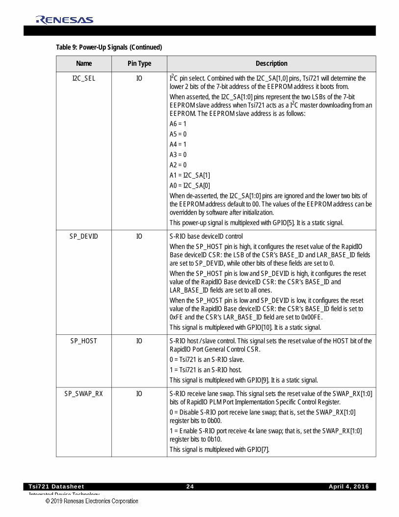
Tsi721 Datasheet 24 April 4, 2016Integrated Device Technology
I2C_SEL IO I2C pin select. Combined with the I2C_SA[1,0] pins, Tsi721 will determine the lower 2 bits of the 7-bit address of the EEPROM address it boots from.
When asserted, the I2C_SA[1:0] pins represent the two LSBs of the 7-bit EEPROM slave address when Tsi721 acts as a I2C master downloading from an EEPROM. The EEPROM slave address is as follows:
A6 = 1
A5 = 0
A4 = 1
A3 = 0
A2 = 0
A1 = I2C_SA[1]
A0 = I2C_SA[0]
When de-asserted, the I2C_SA[1:0] pins are ignored and the lower two bits of the EEPROM address default to 00. The values of the EEPROM address can be overridden by software after initialization.
This power-up signal is multiplexed with GPIO[5]. It is a static signal.
SP_DEVID IO S-RIO base deviceID control
When the SP_HOST pin is high, it configures the reset value of the RapidIO Base deviceID CSR: the LSB of the CSR’s BASE_ID and LAR_BASE_ID fields are set to SP_DEVID, while other bits of these fields are set to 0.
When the SP_HOST pin is low and SP_DEVID is high, it configures the reset value of the RapidIO Base deviceID CSR: the CSR’s BASE_ID and LAR_BASE_ID fields are set to all ones.
When the SP_HOST pin is low and SP_DEVID is low, it configures the reset value of the RapidIO Base deviceID CSR: the CSR’s BASE_ID field is set to 0xFE and the CSR’s LAR_BASE_ID field are set to 0x00FE.
This signal is multiplexed with GPIO[10]. It is a static signal.
SP_HOST IO S-RIO host / slave control. This signal sets the reset value of the HOST bit of the RapidIO Port General Control CSR.
0 = Tsi721 is an S-RIO slave.
1 = Tsi721 is an S-RIO host.
This signal is multiplexed with GPIO[9]. It is a static signal.
SP_SWAP_RX IO S-RIO receive lane swap. This signal sets the reset value of the SWAP_RX[1:0] bits of RapidIO PLM Port Implementation Specific Control Register.
0 = Disable S-RIO port receive lane swap; that is, set the SWAP_RX[1:0] register bits to 0b00.
1 = Enable S-RIO port receive 4x lane swap; that is, set the SWAP_RX[1:0] register bits to 0b10.
This signal is multiplexed with GPIO[7].
Table 9: Power-Up Signals (Continued)
Name Pin Type Description
Tsi721 Datasheet 25 April 4, 2016Integrated Device Technology
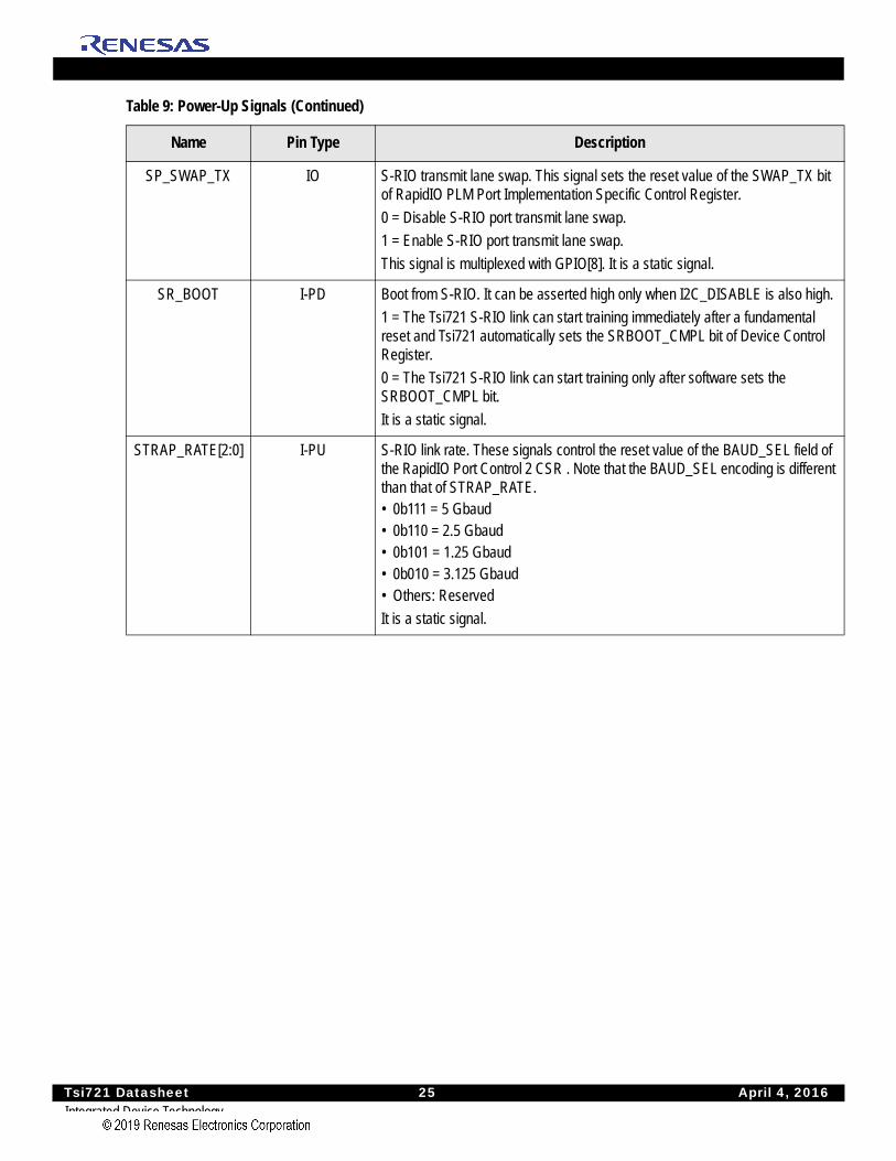
SP_SWAP_TX IO S-RIO transmit lane swap. This signal sets the reset value of the SWAP_TX bit of RapidIO PLM Port Implementation Specific Control Register.
0 = Disable S-RIO port transmit lane swap.
1 = Enable S-RIO port transmit lane swap.
This signal is multiplexed with GPIO[8]. It is a static signal.
SR_BOOT I-PD Boot from S-RIO. It can be asserted high only when I2C_DISABLE is also high.
1 = The Tsi721 S-RIO link can start training immediately after a fundamental reset and Tsi721 automatically sets the SRBOOT_CMPL bit of Device Control Register.
0 = The Tsi721 S-RIO link can start training only after software sets the SRBOOT_CMPL bit.
It is a static signal.
STRAP_RATE[2:0] I-PU S-RIO link rate. These signals control the reset value of the BAUD_SEL field of the RapidIO Port Control 2 CSR . Note that the BAUD_SEL encoding is different than that of STRAP_RATE. • 0b111 = 5 Gbaud• 0b110 = 2.5 Gbaud• 0b101 = 1.25 Gbaud• 0b010 = 3.125 Gbaud• Others: Reserved
It is a static signal.
Table 9: Power-Up Signals (Continued)
Name Pin Type Description
Tsi721 Datasheet 26 April 4, 2016Integrated Device Technology
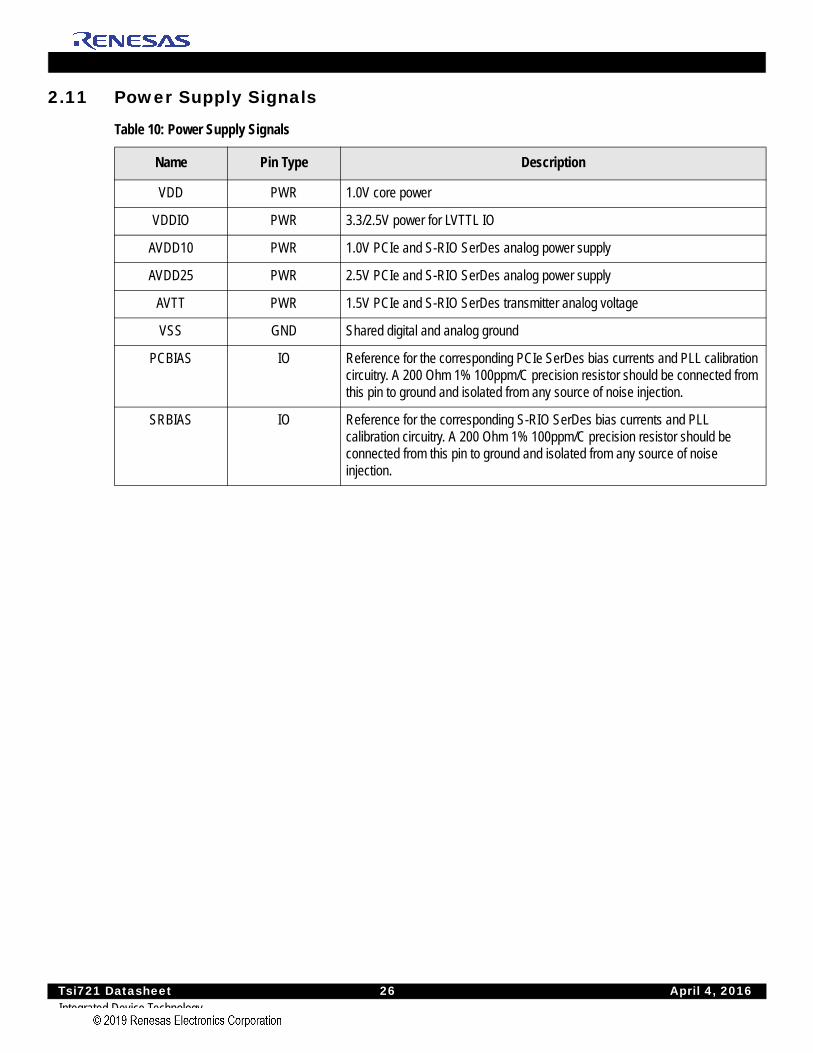
2.11 Power Supply Signals
Table 10: Power Supply Signals
Name Pin Type Description
VDD PWR 1.0V core power
VDDIO PWR 3.3/2.5V power for LVTTL IO
AVDD10 PWR 1.0V PCIe and S-RIO SerDes analog power supply
AVDD25 PWR 2.5V PCIe and S-RIO SerDes analog power supply
AVTT PWR 1.5V PCIe and S-RIO SerDes transmitter analog voltage
VSS GND Shared digital and analog ground
PCBIAS IO Reference for the corresponding PCIe SerDes bias currents and PLL calibration circuitry. A 200 Ohm 1% 100ppm/C precision resistor should be connected from this pin to ground and isolated from any source of noise injection.
SRBIAS IO Reference for the corresponding S-RIO SerDes bias currents and PLL calibration circuitry. A 200 Ohm 1% 100ppm/C precision resistor should be connected from this pin to ground and isolated from any source of noise injection.

Tsi721 Datasheet 27 April 4, 2016Integrated Device Technology
3. Electrical CharacteristicsTopics discussed include the following:
• Absolute Maximum Ratings
• Recommended Operating Conditions
• Power Consumption
• Power Supply Sequencing
• DC Operating Characteristics
• Decoupling Recommendation
• AC Timing Specifications
3.1 Absolute Maximum Ratings
Table 11: Absolute Maximum Ratingsa
a. Stresses outside the absolute ratings can cause permanent damage to the device and affect its functional performance. Exposure to absolute rating conditions for extended periods can affect reliability.
Symbol Parameter Minimum Maximum Units
VDDIO 3.3/2.5V I/O voltage with respect to VSS -0.5 3.6 V
VDD 1.0V core voltage with respect to VSS -0.5 1.10 V
AVDD10 1.0V analog voltage with respect to AVSS -0.5 1.10 V
AVDD25 2.5V analog voltage with respect to AVSS -0.5 2.75 V
AVTT 1.5V analog voltage for SerDes transmitter with respect to AVSS
-0.5 2.75 V
TBIAS Temperature under bias -40 125 C
TSTG Storage temperature -65 150 C
TJN Junction temperature - 125 C
IOUT (for VDDIO = 3.3/2.5V)
DC output current - 30 mA
Tsi721 Datasheet 28 April 4, 2016Integrated Device Technology
3.2 Recommended Operating Conditions
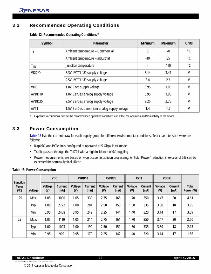
3.3 Power ConsumptionTable 13 lists the current draw for each supply group for different environmental conditions. Test characteristics were are follows:
• RapidIO and PCIe links configured at operated at 5 Gbps in x4 mode
• Traffic passed through the Tsi721 with a high incidence of 0/1 toggling
• Power measurements are based on worst case fast silicon processing. A “Total Power” reduction in excess of 5% can be expected for nominal/typical silicon.
Table 12: Recommended Operating Conditionsa
a. Exposure to conditions outside the recommended operating conditions can affect the operation and/or reliability of the device.
Symbol Parameter Minimum Maximum Units
TA Ambient temperature – Commercial 0 70 C
Ambient temperature – Industrial -40 85 C
TJN Junction temperature - 110 C
VDDIO 3.3V LVTTL I/O supply voltage 3.14 3.47 V
2.5V LVTTL I/O supply voltage 2.4 2.6 V
VDD 1.0V Core supply voltage 0.95 1.05 V
AVDD10 1.0V SerDes analog supply voltage 0.95 1.05 V
AVDD25 2.5V SerDes analog supply voltage 2.25 2.75 V
AVTT 1.5V SerDes transmitter analog supply voltage 1.4 1.7 V
Table 13: Power Consumption
Junction Temp (0C) Voltage
VDD AVDD10 AVDD25 AVTT VDDIO
Total Power (W)
Voltage (V)
Current [mA]
Voltage (V)
Current [mA]
Voltage (V)
Current [mA]
Voltage (V)
Current [mA]
Voltage (V)
Current [mA]
125 Max. 1.05 3000 1.05 330 2.75 165 1.70 350 3.47 20 4.61
Typ. 1.00 2722 1.00 281 2.50 153 1.50 335 3.30 18 3.95
Min. 0.95 2458 0.95 242 2.25 144 1.40 320 3.14 17 3.39
25 Max. 1.05 1110 1.05 214 2.75 161 1.70 350 3.47 20 2.50
Typ. 1.00 1003 1.00 190 2.50 151 1.50 335 3.30 18 2.13
Min. 0.95 909 0.95 170 2.25 142 1.40 320 3.14 17 1.85
Tsi721 Datasheet 29 April 4, 2016Integrated Device Technology
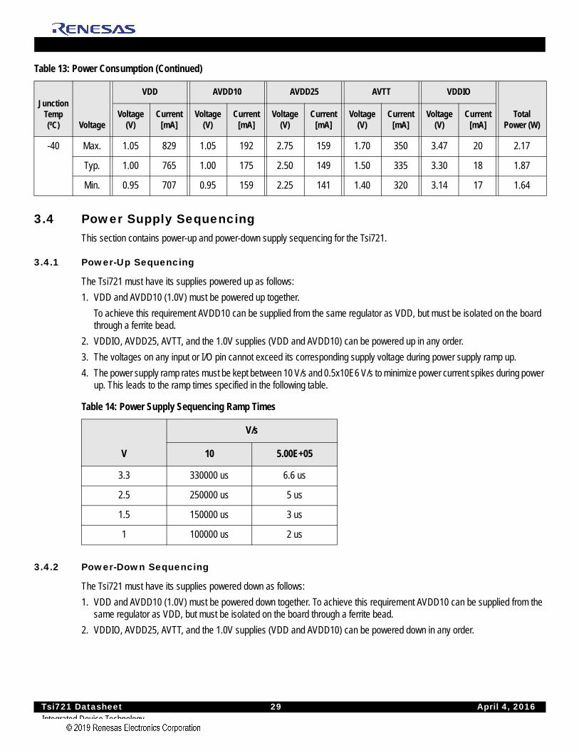
3.4 Power Supply SequencingThis section contains power-up and power-down supply sequencing for the Tsi721.
3.4.1 Power-Up Sequencing
The Tsi721 must have its supplies powered up as follows:
1. VDD and AVDD10 (1.0V) must be powered up together.
To achieve this requirement AVDD10 can be supplied from the same regulator as VDD, but must be isolated on the board through a ferrite bead.
2. VDDIO, AVDD25, AVTT, and the 1.0V supplies (VDD and AVDD10) can be powered up in any order.
3. The voltages on any input or I/O pin cannot exceed its corresponding supply voltage during power supply ramp up.
4. The power supply ramp rates must be kept between 10 V/s and 0.5x10E6 V/s to minimize power current spikes during power up. This leads to the ramp times specified in the following table.
3.4.2 Power-Down Sequencing
The Tsi721 must have its supplies powered down as follows:
1. VDD and AVDD10 (1.0V) must be powered down together. To achieve this requirement AVDD10 can be supplied from the same regulator as VDD, but must be isolated on the board through a ferrite bead.
2. VDDIO, AVDD25, AVTT, and the 1.0V supplies (VDD and AVDD10) can be powered down in any order.
-40 Max. 1.05 829 1.05 192 2.75 159 1.70 350 3.47 20 2.17
Typ. 1.00 765 1.00 175 2.50 149 1.50 335 3.30 18 1.87
Min. 0.95 707 0.95 159 2.25 141 1.40 320 3.14 17 1.64
Table 14: Power Supply Sequencing Ramp Times
V
V/s
10 5.00E+05
3.3 330000 us 6.6 us
2.5 250000 us 5 us
1.5 150000 us 3 us
1 100000 us 2 us
Table 13: Power Consumption (Continued)
Junction Temp (0C) Voltage
VDD AVDD10 AVDD25 AVTT VDDIO
Total Power (W)
Voltage (V)
Current [mA]
Voltage (V)
Current [mA]
Voltage (V)
Current [mA]
Voltage (V)
Current [mA]
Voltage (V)
Current [mA]

Tsi721 Datasheet 30 April 4, 2016Integrated Device Technology
3.5 DC Operating CharacteristicsThe following table lists the DC operating characteristics for 3.3V LVTTL of the Tsi721.
The following table lists the DC operating characteristics for 2.5V LVTTL of the Tsi721.
Table 15: 3.3V LVTTL DC Operating Characteristics at Recommended Operating Condition of 3.3V
Symbol Parameter Minimum Maximum Units
VIH LVTTL input high voltage 2.0 3.6 V
VIL LVTTL input low voltage -0.3 0.8 V
VOH LVTTL output high voltage 2.4 - V
VOL LVTTL output low voltage - 0.4 V
R pull-up Resistor pull-up 26K 64K Ohm
R pull-down Resistor pull-down 29K 79K Ohm
CPAD LVTTL pad capacitance - 4 pF
Table 16: 2.5V LVTTL DC Operating Characteristics at Recommended Operating Condition of 2.5V
Symbol Parameter Minimum Maximum Units
VIH LVTTL input high voltage 1.7 3.6 V
VIL LVTTL input low voltage -0.3 0.7 V
VOH LVTTL output high voltage 1.7 - V
VOL LVTTL output low voltage - 0.7 V
R pull-up Resistor pull-up 33K 93K Ohm
R pull-down Resistor pull-down 34K 108K Ohm
CPAD LVTTL pad capacitance - 4 pF
Tsi721 Datasheet 31 April 4, 2016Integrated Device Technology
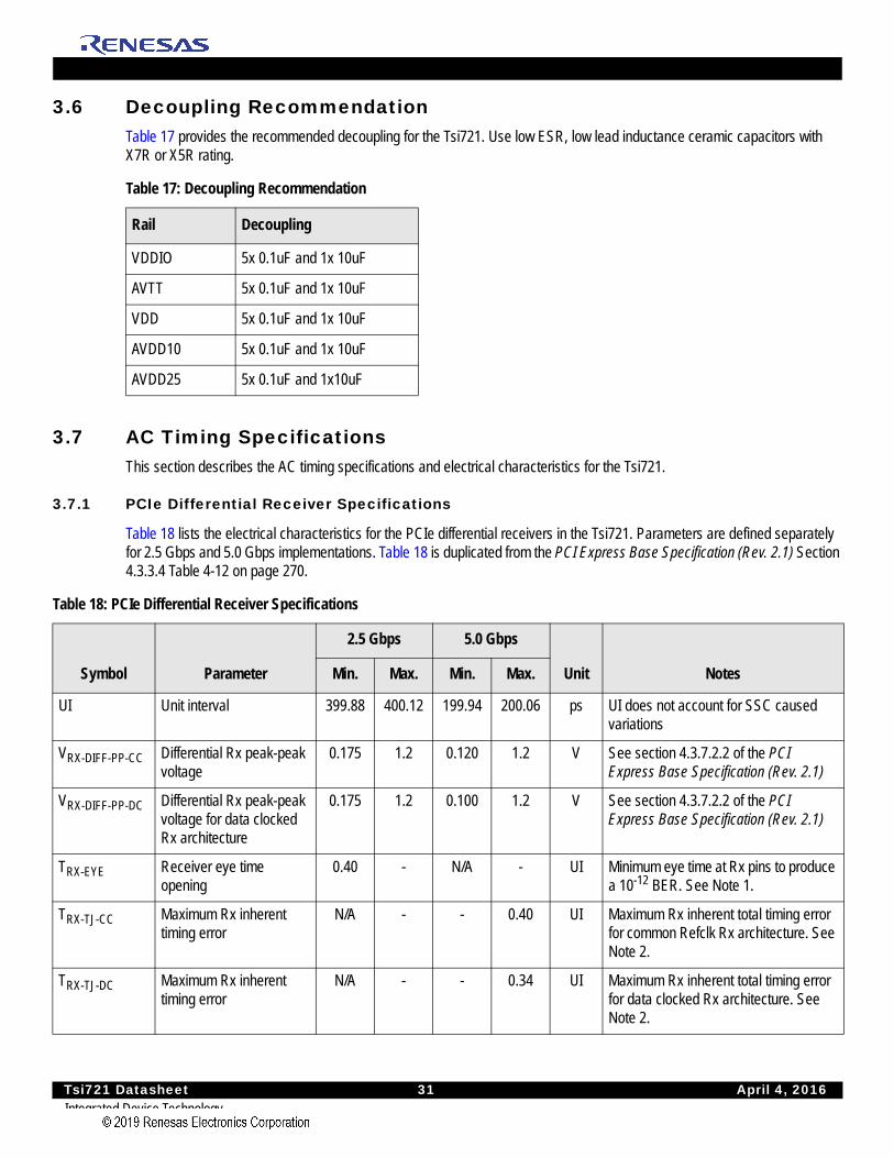
3.6 Decoupling RecommendationTable 17 provides the recommended decoupling for the Tsi721. Use low ESR, low lead inductance ceramic capacitors with X7R or X5R rating.
3.7 AC Timing SpecificationsThis section describes the AC timing specifications and electrical characteristics for the Tsi721.
3.7.1 PCIe Differential Receiver Specifications
Table 18 lists the electrical characteristics for the PCIe differential receivers in the Tsi721. Parameters are defined separately for 2.5 Gbps and 5.0 Gbps implementations. Table 18 is duplicated from the PCI Express Base Specification (Rev. 2.1) Section 4.3.3.4 Table 4-12 on page 270.
Table 17: Decoupling Recommendation
Rail Decoupling
VDDIO 5x 0.1uF and 1x 10uF
AVTT 5x 0.1uF and 1x 10uF
VDD 5x 0.1uF and 1x 10uF
AVDD10 5x 0.1uF and 1x 10uF
AVDD25 5x 0.1uF and 1x10uF
Table 18: PCIe Differential Receiver Specifications
Symbol Parameter
2.5 Gbps 5.0 Gbps
Unit NotesMin. Max. Min. Max.
UI Unit interval 399.88 400.12 199.94 200.06 ps UI does not account for SSC caused variations
VRX-DIFF-PP-CC Differential Rx peak-peak voltage
0.175 1.2 0.120 1.2 V See section 4.3.7.2.2 of the PCI Express Base Specification (Rev. 2.1)
VRX-DIFF-PP-DC Differential Rx peak-peak voltage for data clocked Rx architecture
0.175 1.2 0.100 1.2 V See section 4.3.7.2.2 of the PCI Express Base Specification (Rev. 2.1)
TRX-EYE Receiver eye time opening
0.40 - N/A - UI Minimum eye time at Rx pins to produce a 10-12 BER. See Note 1.
TRX-TJ-CC Maximum Rx inherent timing error
N/A - - 0.40 UI Maximum Rx inherent total timing error for common Refclk Rx architecture. See Note 2.
TRX-TJ-DC Maximum Rx inherent timing error
N/A - - 0.34 UI Maximum Rx inherent total timing error for data clocked Rx architecture. See Note 2.
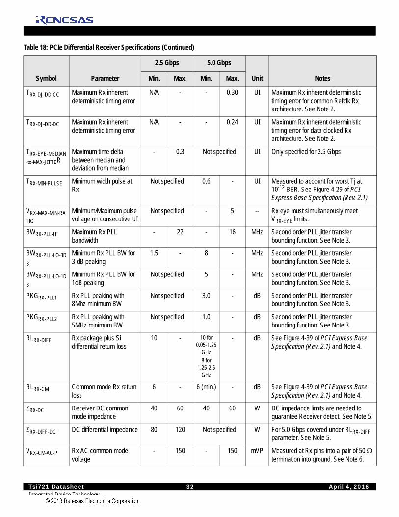
Tsi721 Datasheet 32 April 4, 2016Integrated Device Technology
TRX-DJ-DD-CC Maximum Rx inherent deterministic timing error
N/A - - 0.30 UI Maximum Rx inherent deterministic timing error for common Refclk Rx architecture. See Note 2.
TRX-DJ-DD-DC Maximum Rx inherent deterministic timing error
N/A - - 0.24 UI Maximum Rx inherent deterministic timing error for data clocked Rx architecture. See Note 2.
TRX-EYE-MEDIAN
-to-MAX-JITTERMaximum time delta between median and deviation from median
- 0.3 Not specified UI Only specified for 2.5 Gbps
TRX-MIN-PULSE Minimum width pulse at Rx
Not specified 0.6 - UI Measured to account for worst Tj at 10-12 BER. See Figure 4-29 of PCI Express Base Specification (Rev. 2.1)
VRX-MAX-MIN-RA
TIO
Minimum/Maximum pulse voltage on consecutive UI
Not specified - 5 -- Rx eye must simultaneously meet VRX-EYE limits.
BWRX-PLL-HI Maximum Rx PLL bandwidth
- 22 - 16 MHz Second order PLL jitter transfer bounding function. See Note 3.
BWRX-PLL-LO-3D
B
Minimum Rx PLL BW for 3 dB peaking
1.5 - 8 - MHz Second order PLL jitter transfer bounding function. See Note 3.
BWRX-PLL-LO-1D
B
Minimum Rx PLL BW for 1dB peaking
Not specified 5 - MHz Second order PLL jitter transfer bounding function. See Note 3.
PKGRX-PLL1 Rx PLL peaking with 8Mhz minimum BW
Not specified 3.0 - dB Second order PLL jitter transfer bounding function. See Note 3.
PKGRX-PLL2 Rx PLL peaking with 5MHz minimum BW
Not specified 1.0 - dB Second order PLL jitter transfer bounding function. See Note 3.
RLRX-DIFF Rx package plus Si differential return loss
10 - 10 for 0.05-1.25
GHz
8 for 1.25-2.5
GHz
- dB See Figure 4-39 of PCI Express Base Specification (Rev. 2.1) and Note 4.
RLRX-CM Common mode Rx return loss
6 - 6 (min.) - dB See Figure 4-39 of PCI Express Base Specification (Rev. 2.1) and Note 4.
ZRX-DC Receiver DC common mode impedance
40 60 40 60 W DC impedance limits are needed to guarantee Receiver detect. See Note 5.
ZRX-DIFF-DC DC differential impedance 80 120 Not specified W For 5.0 Gbps covered under RLRX-DIFF parameter. See Note 5.
VRX-CM-AC-P Rx AC common mode voltage
- 150 - 150 mVP Measured at Rx pins into a pair of 50 termination into ground. See Note 6.
Table 18: PCIe Differential Receiver Specifications (Continued)
Symbol Parameter
2.5 Gbps 5.0 Gbps
Unit NotesMin. Max. Min. Max.
Tsi721 Datasheet 33 April 4, 2016Integrated Device Technology
1. Receiver eye margins are defined into a 2 x 50 W reference load. A Receiver is characterized by driving it with a signal whose characteristics are defined by the parameters specified in Table 4-10 and Table 4-11 of the PCI Express Base Specification (Rev. 2.1)
2. The four inherent timing error parameters are defined for the convenience of Rx designers, and they are measured during Receiver tolerancing.
3. Two combinations of PLL BW and peaking are specified at 5.0 Gbps to permit designers to make a trade off between the two parameters. If the PLL’s minimum BW is >= 8MHz, then up to 3.0 dB of peaking is permitted. If the PLL’s minimum BW is relaxed to >= 5.0 MHz, then a tighter peaking value of 1.0 dB must be met. Note: A PLL BW extends from zero up to the value(s) defined as the minimum or maximum in the table. For 2.5 Gbps a single PLL bandwidth and peaking value of 1.5-22 MHz and 3.0 dB are defined.
4. Measurements must be made for both common mode and differential return loss. In both cases the DUT must be powered up and DC isolated, and its D+/D- inputs must be in the low-Z state.
5. The Rx DC Common Mode Impedance must be present when the Receiver terminations are first enabled to ensure that the Receiver Detect occurs properly. Compensation of this impedance can start immediately and the Rx Common Mode Impedance (constrained by RLRX-CM to 50 W +/-20%) must be within the specified range by the time Detect is entered.
6. Common mode peak voltage is defined by the expression: maximum{|(Vd+ - Vd-) - VCMDC|}.
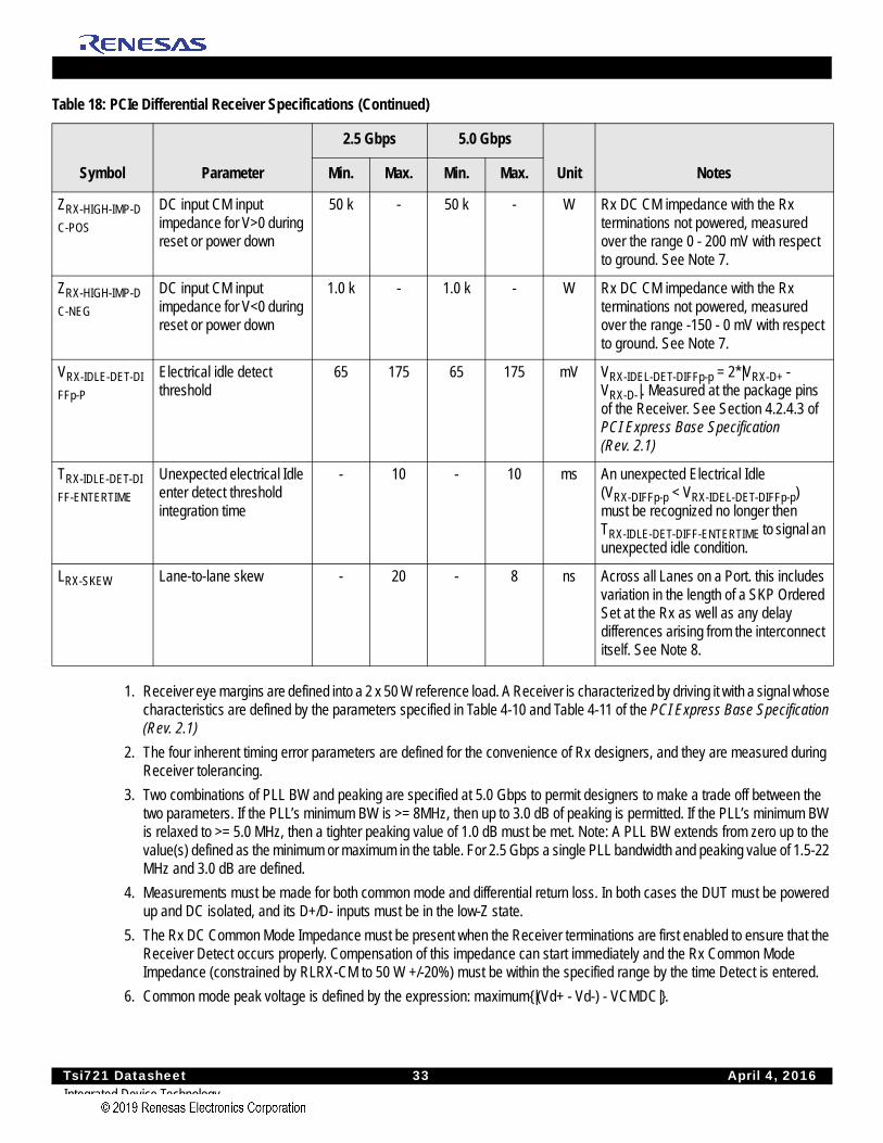
ZRX-HIGH-IMP-D
C-POS
DC input CM input impedance for V>0 during reset or power down
50 k - 50 k - W Rx DC CM impedance with the Rx terminations not powered, measured over the range 0 - 200 mV with respect to ground. See Note 7.
ZRX-HIGH-IMP-D
C-NEG
DC input CM input impedance for V<0 during reset or power down
1.0 k - 1.0 k - W Rx DC CM impedance with the Rx terminations not powered, measured over the range -150 - 0 mV with respect to ground. See Note 7.
VRX-IDLE-DET-DI
FFp-P
Electrical idle detect threshold
65 175 65 175 mV VRX-IDEL-DET-DIFFp-p = 2*|VRX-D+ - VRX-D-|. Measured at the package pins of the Receiver. See Section 4.2.4.3 of PCI Express Base Specification (Rev. 2.1)
TRX-IDLE-DET-DI
FF-ENTERTIME
Unexpected electrical Idle enter detect threshold integration time
- 10 - 10 ms An unexpected Electrical Idle (VRX-DIFFp-p < VRX-IDEL-DET-DIFFp-p) must be recognized no longer then TRX-IDLE-DET-DIFF-ENTERTIME to signal an unexpected idle condition.
LRX-SKEW Lane-to-lane skew - 20 - 8 ns Across all Lanes on a Port. this includes variation in the length of a SKP Ordered Set at the Rx as well as any delay differences arising from the interconnect itself. See Note 8.
Table 18: PCIe Differential Receiver Specifications (Continued)
Symbol Parameter
2.5 Gbps 5.0 Gbps
Unit NotesMin. Max. Min. Max.
Tsi721 Datasheet 34 April 4, 2016Integrated Device Technology
7. ZRX-HIGH-IMP-DC-NEG and ZRX-HIGH-IMP-DC-POS are defined respectively for negative and positive voltages at the input of the Receiver. Transmitter designers need to comprehend the large difference between >0 and <0 Rx impedances when designing Receiver detect circuits.
8. The LRX-SKEW parameter exists to handle repeaters that regenerate Refclk and introduce differing numbers of skips on different lanes.
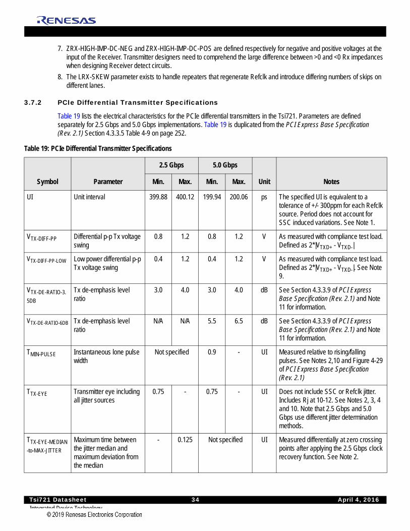
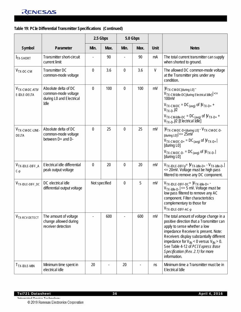
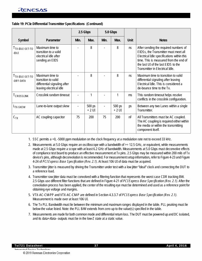
3.7.2 PCIe Differential Transmitter Specifications
Table 19 lists the electrical characteristics for the PCIe differential transmitters in the Tsi721. Parameters are defined separately for 2.5 Gbps and 5.0 Gbps implementations. Table 19 is duplicated from the PCI Express Base Specification (Rev. 2.1) Section 4.3.3.5 Table 4-9 on page 252.
Table 19: PCIe Differential Transmitter Specifications
Symbol Parameter
2.5 Gbps 5.0 Gbps
Unit NotesMin. Max. Min. Max.
UI Unit interval 399.88 400.12 199.94 200.06 ps The specified UI is equivalent to a tolerance of +/- 300ppm for each Refclk source. Period does not account for SSC induced variations. See Note 1.
VTX-DIFF-PP Differential p-p Tx voltage swing
0.8 1.2 0.8 1.2 V As measured with compliance test load. Defined as 2*|VTXD+ - VTXD-|
VTX-DIFF-PP-LOW Low power differential p-p Tx voltage swing
0.4 1.2 0.4 1.2 V As measured with compliance test load. Defined as 2*|VTXD+ - VTXD-|. See Note 9.
VTX-DE-RATIO-3.
5DB
Tx de-emphasis level ratio
3.0 4.0 3.0 4.0 dB See Section 4.3.3.9 of PCI Express Base Specification (Rev. 2.1) and Note 11 for information.
VTX-DE-RATIO-6DB Tx de-emphasis level ratio
N/A N/A 5.5 6.5 dB See Section 4.3.3.9 of PCI Express Base Specification (Rev. 2.1) and Note 11 for information.
TMIN-PULSE Instantaneous lone pulse width
Not specified 0.9 - UI Measured relative to rising/falling pulses. See Notes 2,10 and Figure 4-29 of PCI Express Base Specification (Rev. 2.1)
TTX-EYE Transmitter eye including all jitter sources
0.75 - 0.75 - UI Does not include SSC or Refclk jitter. Includes Rj at 10-12. See Notes 2, 3, 4 and 10. Note that 2.5 Gbps and 5.0 Gbps use different jitter determination methods.
TTX-EYE-MEDIAN
-to-MAX-JITTER
Maximum time between the jitter median and maximum deviation from the median
- 0.125 Not specified UI Measured differentially at zero crossing points after applying the 2.5 Gbps clock recovery function. See Note 2.
Tsi721 Datasheet 35 April 4, 2016Integrated Device Technology
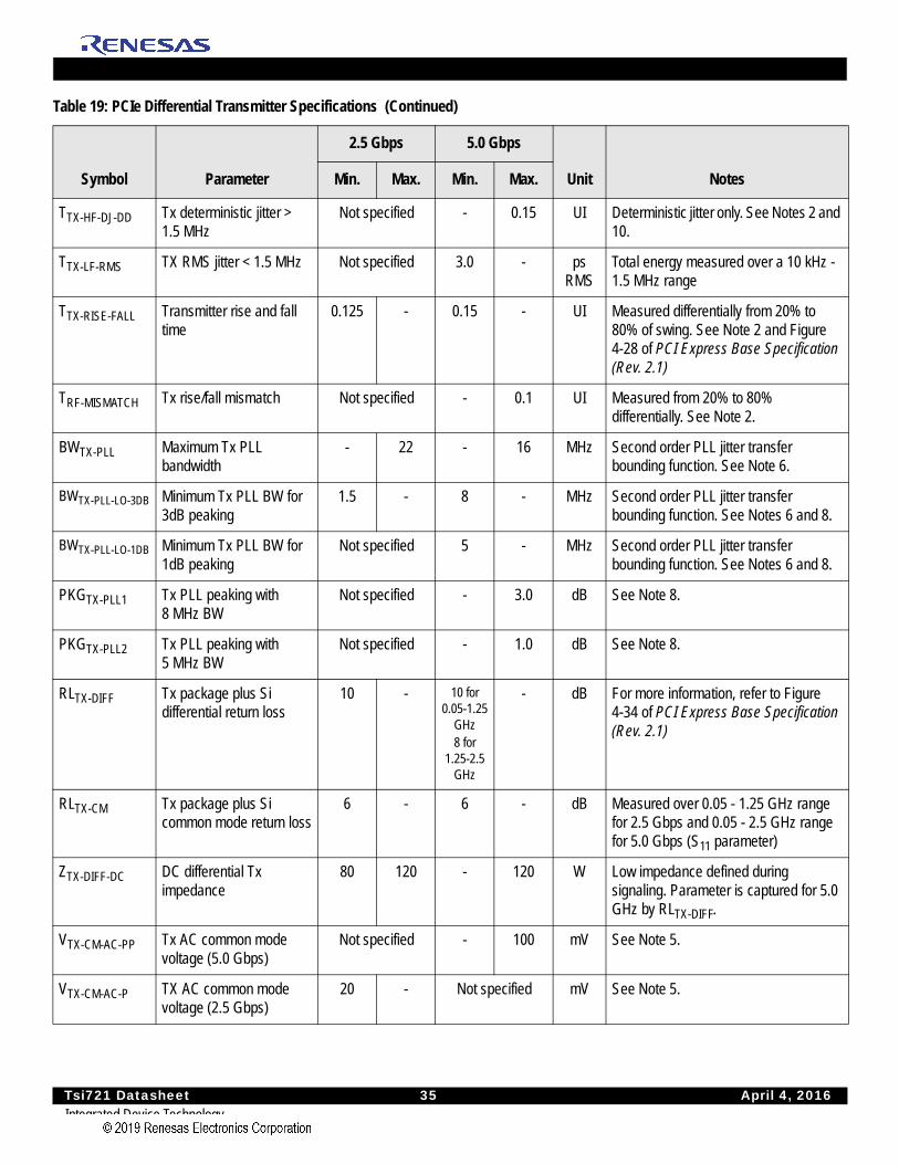
TTX-HF-DJ-DD Tx deterministic jitter > 1.5 MHz
Not specified - 0.15 UI Deterministic jitter only. See Notes 2 and 10.
TTX-LF-RMS TX RMS jitter < 1.5 MHz Not specified 3.0 - ps RMS
Total energy measured over a 10 kHz - 1.5 MHz range
TTX-RISE-FALL Transmitter rise and fall time
0.125 - 0.15 - UI Measured differentially from 20% to 80% of swing. See Note 2 and Figure 4-28 of PCI Express Base Specification (Rev. 2.1)
TRF-MISMATCH Tx rise/fall mismatch Not specified - 0.1 UI Measured from 20% to 80% differentially. See Note 2.
BWTX-PLL Maximum Tx PLL bandwidth
- 22 - 16 MHz Second order PLL jitter transfer bounding function. See Note 6.
BWTX-PLL-LO-3DB Minimum Tx PLL BW for 3dB peaking
1.5 - 8 - MHz Second order PLL jitter transfer bounding function. See Notes 6 and 8.
BWTX-PLL-LO-1DB Minimum Tx PLL BW for 1dB peaking
Not specified 5 - MHz Second order PLL jitter transfer bounding function. See Notes 6 and 8.
PKGTX-PLL1 Tx PLL peaking with 8 MHz BW
Not specified - 3.0 dB See Note 8.
PKGTX-PLL2 Tx PLL peaking with 5 MHz BW
Not specified - 1.0 dB See Note 8.
RLTX-DIFF Tx package plus Si differential return loss
10 - 10 for 0.05-1.25
GHz8 for
1.25-2.5 GHz
- dB For more information, refer to Figure 4-34 of PCI Express Base Specification (Rev. 2.1)
RLTX-CM Tx package plus Si common mode return loss
6 - 6 - dB Measured over 0.05 - 1.25 GHz range for 2.5 Gbps and 0.05 - 2.5 GHz range for 5.0 Gbps (S11 parameter)
ZTX-DIFF-DC DC differential Tx impedance
80 120 - 120 W Low impedance defined during signaling. Parameter is captured for 5.0 GHz by RLTX-DIFF.
VTX-CM-AC-PP Tx AC common mode voltage (5.0 Gbps)
Not specified - 100 mV See Note 5.
VTX-CM-AC-P TX AC common mode voltage (2.5 Gbps)
20 - Not specified mV See Note 5.
Table 19: PCIe Differential Transmitter Specifications (Continued)
Symbol Parameter
2.5 Gbps 5.0 Gbps
Unit NotesMin. Max. Min. Max.
Tsi721 Datasheet 36 April 4, 2016Integrated Device Technology
ITX-SHORT Transmitter short-circuit current limit
- 90 - 90 mA The total current transmitter can supply when shorted to ground.
VTX-DC-CM Transmitter DC common-mode voltage
0 3.6 0 3.6 V The allowed DC common-mode voltage at the Transmitter pins under any condition.
VTX-CM-DC-ATIV
E-IDLE-DELTA
Absolute delta of DC common-mode voltage during L0 and Electrical Idle
0 100 0 100 mV |VTX-CM-DC[during L0] - VTX-CM-Idle-DC[during Electrical Idle]| <= 100mV
VTX-CM-DC = DC(avg) of |VTX-D+ + VTX-D-|/2
VTX-CM-Idle-DC = DC(avg) of |VTX-D+ + VTX-D-|/2 [Electrical Idle]
VTX-CM-DC-LINE-
DELTA
Absolute delta of DC common-mode voltage between D+ and D-
0 25 0 25 mV |VTX-CM-DC-D+[during L0] - VTX-CM-DC-D-
[during L0]| <= 25mV
VTX-CM-DC-D+ = DC(avg) of |VTX-D+| [during L0]
VTX-CM-DC-D- = DC(avg) of |VTX-D-| [during L0]
VTX-IDLE-DIFF_A
C-p
Electrical idle differential peak output voltage
0 20 0 20 mV VTX-IDLE-DIFFp= |VTX-Idle-D+ - VTX-Idle-D-| <= 20mV. Voltage must be high pass filtered to remove any DC component.
VTX-IDLE-DIFF_DC DC electrical idle differential output voltage
Not specified 0 5 mV VTX-IDLE-DIFF-DC= |VTX-Idle-D+ - VTX-Idle-D-| <= 5 mV. Voltage must be low pass filtered to remove any AC component. Filter characteristics complementary to those for VTX-IDLE-DIFF-AC-p
VTX-RCV-DETECT The amount of voltage change allowed during receiver detection
- 600 - 600 mV The total amount of voltage change in a positive direction that a Transmitter can apply to sense whether a low impedance Receiver is present. Note: Receivers display substantially different impedance for VIN < 0 versus VIN > 0. See Table 4-12 of PCI Express Base Specification (Rev. 2.1) for more information.
TTX-IDLE-MIN Minimum time spent in electrical idle
20 - 20 - ns Minimum time a Transmitter must be in Electrical Idle
Table 19: PCIe Differential Transmitter Specifications (Continued)
Symbol Parameter
2.5 Gbps 5.0 Gbps
Unit NotesMin. Max. Min. Max.
Tsi721 Datasheet 37 April 4, 2016Integrated Device Technology
1. SSC permits a +0, -5000 ppm modulation on the clock frequency at a modulation rate not to exceed 33 kHz.
2. Measurements at 5.0 Gbps require an oscilloscope with a bandwidth of >= 12.5 GHz, or equivalent, while measurements made at 2.5 Gbps require a scope with at least 6.2 GHz of bandwidth. Measurements at 5.0 Gbps must deconvolve effects of compliance test board to produce an effective measurement at Tx pins. 2.5 Gbps may be measured within 200 mils of Tx device’s pins, although deconvolution is recommended. For measurement setup information, refer to Figure 4-23 and Figure 4-24 of PCI Express Base Specification (Rev. 2.1). At least 106 UI of data must be acquired.
3. Transmitter jitter is measured by driving the Transmitter under test with a low jitter “ideal” clock and connecting the DUT to a reference load.
4. Transmitter raw jitter data must be convolved with a filtering function that represents the worst case CDR tracking BW. 2.5 Gbps use different filter functions that are defined in Figure 4-21 of PCI Express Base Specification (Rev. 2.1). After the convolution process has been applied, the center of the resulting eye must be determined and used as a reference point for obtaining eye voltage and margins.
5. VTX-AC-CM-PP and VTX-AC-CM-P are defined in Section 4.3.3.7 of PCI Express Base Specification (Rev. 2.1). Measurement is made over at least 106 UI.
6. The Tx PLL Bandwidth must lie between the minimum and maximum ranges displayed in the table. PLL peaking must lie below the value listed. Note: the PLL B/W extends from zero up to the value(s) specified in the table.
7. Measurements are made for both common mode and differential return loss. The DUT must be powered up and DC isolated, and its data+/data- outputs must be in the low-Z state at a static value.
TTX-IDLE-SET-TO
-IDLE
Maximum time to transition to a valid electrical idle after sending an EIOS
- 8 - 8 ns After sending the required numbers of EIOSs, the Transmitter must meet all Electrical Idle specifications within this time. This is measured from the end of the last UI of the last EIOS to the Transmitter in Electrical Idle.
TTX-IDLE-SET-TO
-DIFF-DATA
Maximum time to transition to valid differential signaling after leaving electrical idle
- 8 - 8 ns Maximum time to transition to valid differential signaling after leaving Electrical Idle. This is considered a de-bounce time to the Tx.
TCROSSLINK Crosslink random timeout - 1 - 1 ms This random timeout helps resolve conflicts in the crosslink configuration.
LTX-SKEW Lane-to-lane output skew - 500 ps + 2 UI
- 500 ps + 2 UI
ps Between any two Lanes within a single Transmitter.
CTX AC coupling capacitor 75 200 75 200 nF All Transmitters must be AC coupled. The AC coupling is required either within the media or within the transmitting component itself.
Table 19: PCIe Differential Transmitter Specifications (Continued)
Symbol Parameter
2.5 Gbps 5.0 Gbps
Unit NotesMin. Max. Min. Max.
Tsi721 Datasheet 38 April 4, 2016Integrated Device Technology
8. A single combination of PLL BW and peaking is specified for 2.5 Gbps implementations. For 5.0 Gbps, two combinations of PLL BW and peaking are specified to permit designers to make a trade-off between the two parameters. If the PLL’s minimum BW is >= 8MHz, the up to 3.0 dB of peaking is permitted. If the PLL’s minimum BW is related to >= 5.0 MHz, then a tighter peaking value of 1.0 dB must be met. In both cases, the maximum PLL BW is 16 MHz.
9. Low swing output, defined by VTX-DIFF-PP-LOW must be implemented as displayed in Figure 4-27 of the PCI Express Base Specification (Rev. 2.1) with no de-emphasis.
10.For 5.0 Gbps, de-emphasis timing jitter must be removed. An additional HPF function must be applied as displayed in Figure 4-21 of PCI Express Base Specification (Rev. 2.1). This parameter is measured by accumulating a record of 106 UI while the DUT outputs a compliance pattern. TMIN-PULSE is defined to be nominally 1 UI wide and is bordered on both sides by pulses of the opposite polarity. Refer to Figure 4-29 of PCI Express Base Specification (Rev. 2.1).
11. Root complex Tx de-emphasis is configured from Upstream controller. Downstream Tx de-emphasis is set through a command, issues at 2.5 Gbps. For information, refer to the appropriate location in Section 4.2 of PCI Express Base Specification (Rev. 2.1).
3.7.3 RapidIO SerDes Characteristics
3.7.3.1 Overview
The Tsi721’s SerDes are in full compliance to the RapidIO AC specifications for the LP-Serial physical layer [5]. This section provides those specifications for reference only; the user should see the specification for complete requirements.
Chapter 9 of the specification, “1.25 Gbaud, 2.5 Gbaud, and 3.125 Gbaud LP-Serial Links” defines Level I links compatible with the 1.3 version of the Physical Layer Specification, that supports throughput rates of 1.25, 2.5, and 3.125 Gbps. Chapter 10 of the specification, “5 Gbaud and 6.25 Gbaud LP-Serial Links” defines Level II links that support throughput rates of 5 and 6.25 Gbps.
A Level I link should:
• Allow 1.25, 2.5, or 3.125 Gbps rates
• Support AC coupling
• Support hot plug
• Support short run (SR) and long run (LR) links achieved with two transmitters
• Support single receiver specification that will accept signals from both the short run and long run transmitter specifications
• Achieve Bit Error Ratio of lower than 10-12 per lane
A Level II link should:
• Allow 5 Gbps baud rates
• Support AC coupling and optional DC coupling
• Support hot plug
• Support short run (SR), and medium run (MR) links achieved with two transmitters and two receivers
• Achieve Bit Error Ratio of lower than 10-15 per lane but test requirements will be verified to 10-12 per lane
Together, these specifications allow for solutions ranging from simple chip-to-chip interconnect to board-to-board interconnect driving two connectors across a backplane. The faster and wider electrical interfaces specified here are required to provide higher density and/or lower cost interfaces.
The short run defines a transmitter and a receiver that should be used mainly for chip-to-chip connections on either the same printed circuit board or across a single connector. This covers the case where connections are made to a mezzanine (daughter) card. The smaller swings of the short run specification reduces the overall power used by the transceivers.
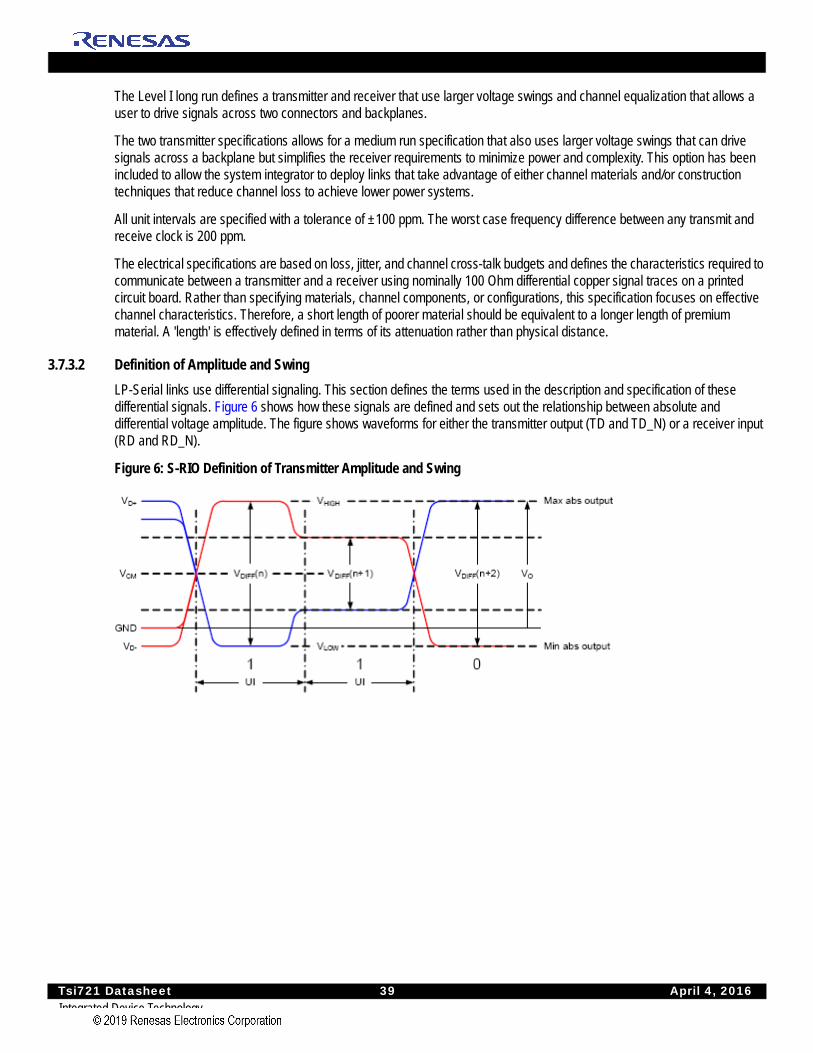
Tsi721 Datasheet 39 April 4, 2016Integrated Device Technology
The Level I long run defines a transmitter and receiver that use larger voltage swings and channel equalization that allows a user to drive signals across two connectors and backplanes.
The two transmitter specifications allows for a medium run specification that also uses larger voltage swings that can drive signals across a backplane but simplifies the receiver requirements to minimize power and complexity. This option has been included to allow the system integrator to deploy links that take advantage of either channel materials and/or construction techniques that reduce channel loss to achieve lower power systems.
All unit intervals are specified with a tolerance of ±100 ppm. The worst case frequency difference between any transmit and receive clock is 200 ppm.
The electrical specifications are based on loss, jitter, and channel cross-talk budgets and defines the characteristics required to communicate between a transmitter and a receiver using nominally 100 Ohm differential copper signal traces on a printed circuit board. Rather than specifying materials, channel components, or configurations, this specification focuses on effective channel characteristics. Therefore, a short length of poorer material should be equivalent to a longer length of premium material. A 'length' is effectively defined in terms of its attenuation rather than physical distance.
3.7.3.2 Definition of Amplitude and Swing
LP-Serial links use differential signaling. This section defines the terms used in the description and specification of these differential signals. Figure 6 shows how these signals are defined and sets out the relationship between absolute and differential voltage amplitude. The figure shows waveforms for either the transmitter output (TD and TD_N) or a receiver input (RD and RD_N).
Figure 6: S-RIO Definition of Transmitter Amplitude and Swing
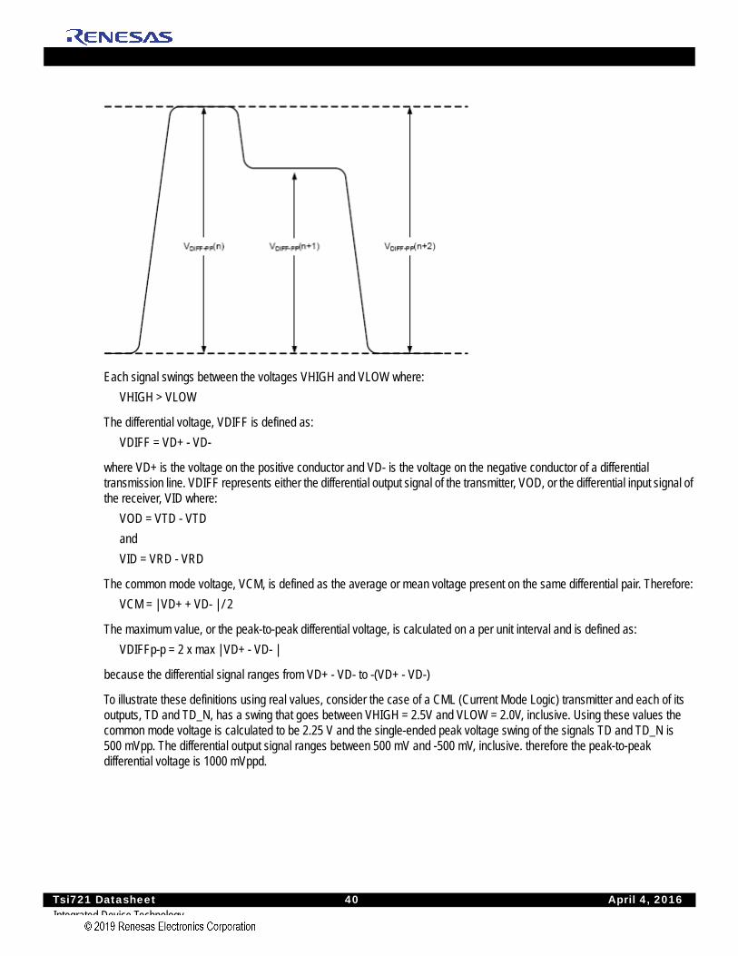
Tsi721 Datasheet 40 April 4, 2016Integrated Device Technology
Each signal swings between the voltages VHIGH and VLOW where:
VHIGH > VLOW
The differential voltage, VDIFF is defined as:
VDIFF = VD+ - VD-
where VD+ is the voltage on the positive conductor and VD- is the voltage on the negative conductor of a differential transmission line. VDIFF represents either the differential output signal of the transmitter, VOD, or the differential input signal of the receiver, VID where:
VOD = VTD - VTD
and
VID = VRD - VRD
The common mode voltage, VCM, is defined as the average or mean voltage present on the same differential pair. Therefore:
VCM = | VD+ + VD- | / 2
The maximum value, or the peak-to-peak differential voltage, is calculated on a per unit interval and is defined as:
VDIFFp-p = 2 x max | VD+ - VD- |
because the differential signal ranges from VD+ - VD- to -(VD+ - VD-)
To illustrate these definitions using real values, consider the case of a CML (Current Mode Logic) transmitter and each of its outputs, TD and TD_N, has a swing that goes between VHIGH = 2.5V and VLOW = 2.0V, inclusive. Using these values the common mode voltage is calculated to be 2.25 V and the single-ended peak voltage swing of the signals TD and TD_N is 500 mVpp. The differential output signal ranges between 500 mV and -500 mV, inclusive. therefore the peak-to-peak differential voltage is 1000 mVppd.
Tsi721 Datasheet 41 April 4, 2016Integrated Device Technology
3.7.3.3 1.25 Gbps, 2.5 Gbps, and 3.125 Gbps LP-Serial Links
This section explains the requirements for Level I RapidIO LP-Serial short and long run electrical interfaces of nominal baud rates of 1.25, 2.5, and 3.125 Gbps using NRZ coding (thus, 1 bit per symbol at the electrical level). The Tsi721’s SerDes meet all of the requirements listed below. The electrical interface is based on a high speed, low voltage logic with a nominal differential impedance of 100 Ohm. Connections are point-to-point balanced differential pair and signaling is unidirectional.
The level of links defined in this section are identical to those defined in the RapidIO Interconnect Specification (Revision 2.1), 1x/4x LP-Serial Electrical Specification.
3.7.3.4 Equalization
With the use of high speed serial links, the interconnect media will cause degradation of the signal at the receiver. Effects such as Inter-Symbol Interference (ISI) or data dependent jitter are produced. This loss can be large enough to degrade the eye opening at the receiver beyond what is allowed in the specification. To negate a portion of these effects, equalization can be used in the transmitter and/or receiver, but it is not required at baud rates less than 3.125 Gbps.
3.7.3.5 Explanatory Note on Level I Transmitter and Receiver Specifications
AC electrical specifications are provided for the transmitter and receiver. Long run and short run interfaces at three baud rates are described.
The parameters for the AC electrical specifications are guided by the XAUI electrical interface specified in Clause 47 of IEEE 802.3ae-2002.[1] The goal of this standard is that electrical designs for Level I electrical designs can reuse XAUI, suitably modified for applications at the baud intervals and runs described herein.
3.7.3.6 Level I Electrical Specification
3.7.3.6.1 Level I Transmitter Characteristics
Level I LP-Serial transmitter electrical and timing specifications are stated in the text and tables of this section. The differential return loss, S11, of the transmitter in each case must be better than:
• -10 dB for (Baud Frequency) / 10 < Freq(f) < 625 MHz, and
• -10 dB + 10log(f/625 MHz) dB for 625 MHz <= Freq(f) <= Baud Frequency
The reference impedance for the differential return loss measurements is 100 Ohm resistive. Differential return loss includes contributions from on-chip circuitry, chip packaging and any off-chip components related to the driver. The output impedance requirement applies to all valid output levels.
The Tsi721 satisfies the specification requirement that the 20%-80% rise/fall time of the transmitter, as measured at the transmitter output, in each case has a minimum value 60 ps.
Similarly, the timing skew at the output of an LP-Serial transmitter between the two signals that comprise a differential pair does not exceed 25 ps at 1.25 Gbps, 20 ps at 2.5 Gbps, and 15 ps at 3.125 Gbps.
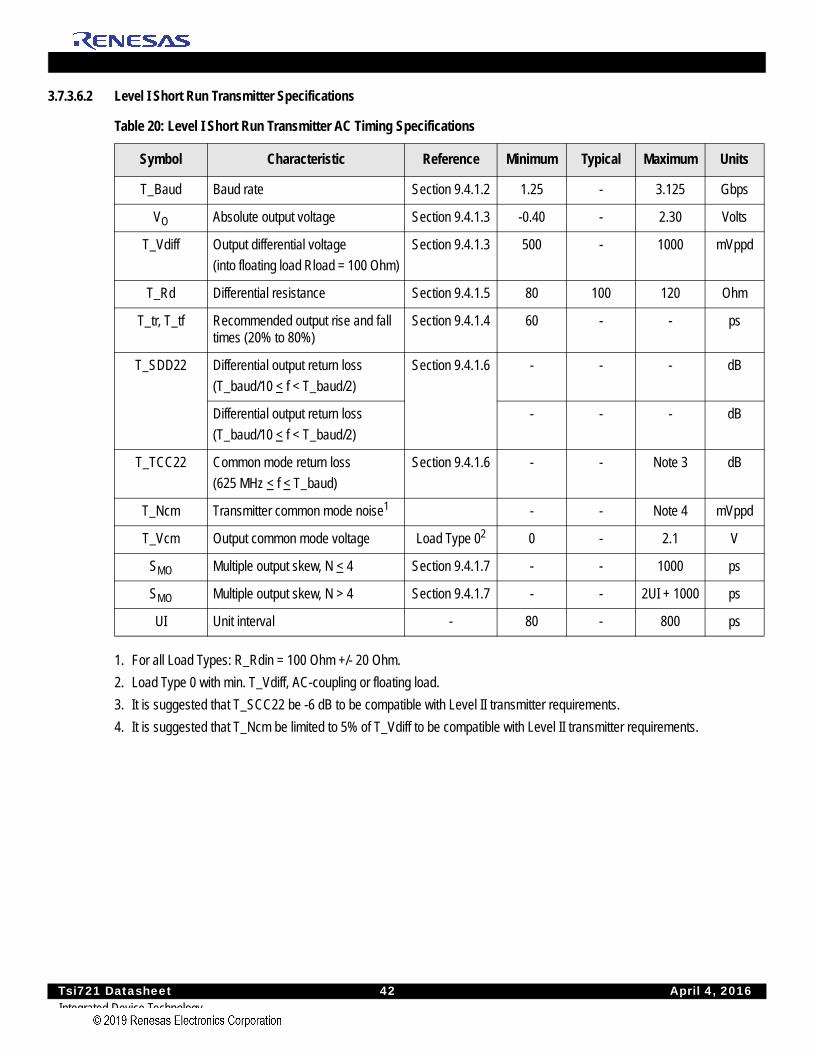
Tsi721 Datasheet 42 April 4, 2016Integrated Device Technology
3.7.3.6.2 Level I Short Run Transmitter Specifications
1. For all Load Types: R_Rdin = 100 Ohm +/- 20 Ohm.
2. Load Type 0 with min. T_Vdiff, AC-coupling or floating load.
3. It is suggested that T_SCC22 be -6 dB to be compatible with Level II transmitter requirements.
4. It is suggested that T_Ncm be limited to 5% of T_Vdiff to be compatible with Level II transmitter requirements.
Table 20: Level I Short Run Transmitter AC Timing Specifications
Symbol Characteristic Reference Minimum Typical Maximum Units
T_Baud Baud rate Section 9.4.1.2 1.25 - 3.125 Gbps
VO Absolute output voltage Section 9.4.1.3 -0.40 - 2.30 Volts
T_Vdiff Output differential voltage
(into floating load Rload = 100 Ohm)
Section 9.4.1.3 500 - 1000 mVppd
T_Rd Differential resistance Section 9.4.1.5 80 100 120 Ohm
T_tr, T_tf Recommended output rise and fall times (20% to 80%)
Section 9.4.1.4 60 - - ps
T_SDD22 Differential output return loss
(T_baud/10 < f < T_baud/2)
Section 9.4.1.6 - - - dB
Differential output return loss
(T_baud/10 < f < T_baud/2)
- - - dB
T_TCC22 Common mode return loss
(625 MHz < f < T_baud)
Section 9.4.1.6 - - Note 3 dB
T_Ncm Transmitter common mode noise1 - - Note 4 mVppd
T_Vcm Output common mode voltage Load Type 02 0 - 2.1 V
SMO Multiple output skew, N < 4 Section 9.4.1.7 - - 1000 ps
SMO Multiple output skew, N > 4 Section 9.4.1.7 - - 2UI + 1000 ps
UI Unit interval - 80 - 800 ps
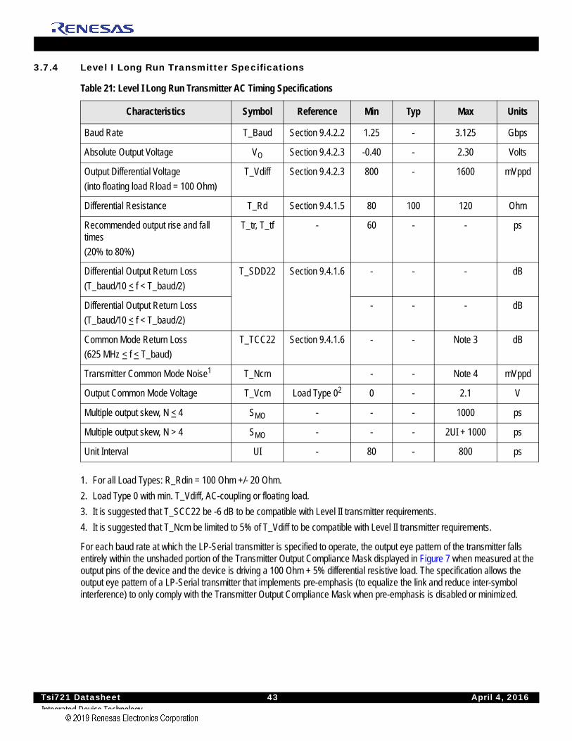
Tsi721 Datasheet 43 April 4, 2016Integrated Device Technology
3.7.4 Level I Long Run Transmitter Specifications
1. For all Load Types: R_Rdin = 100 Ohm +/- 20 Ohm.
2. Load Type 0 with min. T_Vdiff, AC-coupling or floating load.
3. It is suggested that T_SCC22 be -6 dB to be compatible with Level II transmitter requirements.
4. It is suggested that T_Ncm be limited to 5% of T_Vdiff to be compatible with Level II transmitter requirements.
For each baud rate at which the LP-Serial transmitter is specified to operate, the output eye pattern of the transmitter falls entirely within the unshaded portion of the Transmitter Output Compliance Mask displayed in Figure 7 when measured at the output pins of the device and the device is driving a 100 Ohm + 5% differential resistive load. The specification allows the output eye pattern of a LP-Serial transmitter that implements pre-emphasis (to equalize the link and reduce inter-symbol interference) to only comply with the Transmitter Output Compliance Mask when pre-emphasis is disabled or minimized.
Table 21: Level I Long Run Transmitter AC Timing Specifications
Characteristics Symbol Reference Min Typ Max Units
Baud Rate T_Baud Section 9.4.2.2 1.25 - 3.125 Gbps
Absolute Output Voltage VO Section 9.4.2.3 -0.40 - 2.30 Volts
Output Differential Voltage
(into floating load Rload = 100 Ohm)
T_Vdiff Section 9.4.2.3 800 - 1600 mVppd
Differential Resistance T_Rd Section 9.4.1.5 80 100 120 Ohm
Recommended output rise and fall times
(20% to 80%)
T_tr, T_tf - 60 - - ps
Differential Output Return Loss
(T_baud/10 < f < T_baud/2)
T_SDD22 Section 9.4.1.6 - - - dB
Differential Output Return Loss
(T_baud/10 < f < T_baud/2)
- - - dB
Common Mode Return Loss
(625 MHz < f < T_baud)
T_TCC22 Section 9.4.1.6 - - Note 3 dB
Transmitter Common Mode Noise1 T_Ncm - - Note 4 mVppd
Output Common Mode Voltage T_Vcm Load Type 02 0 - 2.1 V
Multiple output skew, N < 4 SMO - - - 1000 ps
Multiple output skew, N > 4 SMO - - - 2UI + 1000 ps
Unit Interval UI - 80 - 800 ps
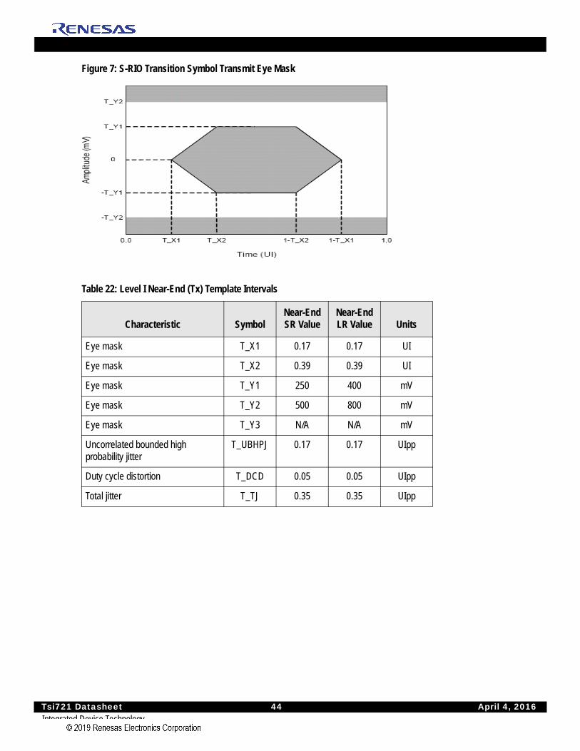
Tsi721 Datasheet 44 April 4, 2016Integrated Device Technology
Figure 7: S-RIO Transition Symbol Transmit Eye Mask
Table 22: Level I Near-End (Tx) Template Intervals
Characteristic SymbolNear-EndSR Value
Near-EndLR Value Units
Eye mask T_X1 0.17 0.17 UI
Eye mask T_X2 0.39 0.39 UI
Eye mask T_Y1 250 400 mV
Eye mask T_Y2 500 800 mV
Eye mask T_Y3 N/A N/A mV
Uncorrelated bounded high probability jitter
T_UBHPJ 0.17 0.17 UIpp
Duty cycle distortion T_DCD 0.05 0.05 UIpp
Total jitter T_TJ 0.35 0.35 UIpp
Tsi721 Datasheet 45 April 4, 2016Integrated Device Technology
3.7.4.0.1 Level I Receiver Specifications
Level I LP-Serial receiver electrical and timing specifications are stated in the text and tables of this section.
1. Input common mode voltage for AC-coupled or floating load input with min. T_Vdiff.
2. Receiver is required to implement at least one of the specified nominal R_Vtt values, and usually implements only one of these values. Receiver is only required to meet R_Vrcm parameter values that correspond to R_Vtt values supported.
3. Input common mode voltage for AC-coupled or floating load input with min. T_Vdiff.
4. For floating load, input resistance must be > 1K Ohm.
Table 23: Level I Receiver Electrical Input Specifications
Characteristic Symbol Reference Minimum Typical Maximum Units
Rx baud rate (1.25 Gbps) R_Baud - - 1.250 - Gbps
Rx baud rate (2.5 Gbps) - - 2.500 - Gbps
Rx baud rate (3.125 Gbps) - - 3.125 - Gbps
Absolute input voltage R_Vin Section 9.4.3.4
- - - -
Input differential voltage R_Vdiff Section 9.4.3.3
200 - 1600 mVppd
Differential resistance R_Rdin Section 9.4.3.7
80 100 120 Ohm
Differential input return loss
(100 MHz < f < R_Baud/2)
R_SDD11 Section 9.4.3.7
- - - dB
Differential input return loss
(R_Baud/2 < f < R_Baud)
- - - -
Common mode input return loss
(625 MHz < f < T_baud)
R_SCC11 Section 9.4.3.7
- - - dB
Termination voltage1,2 R_Vtt R_Vtt floating4
Not specified V
Input common mode voltage1,2 R_Vrcm R_Vtt floating3,4
-0.05 - 1.85 V
Wander divider n - - 10 - -
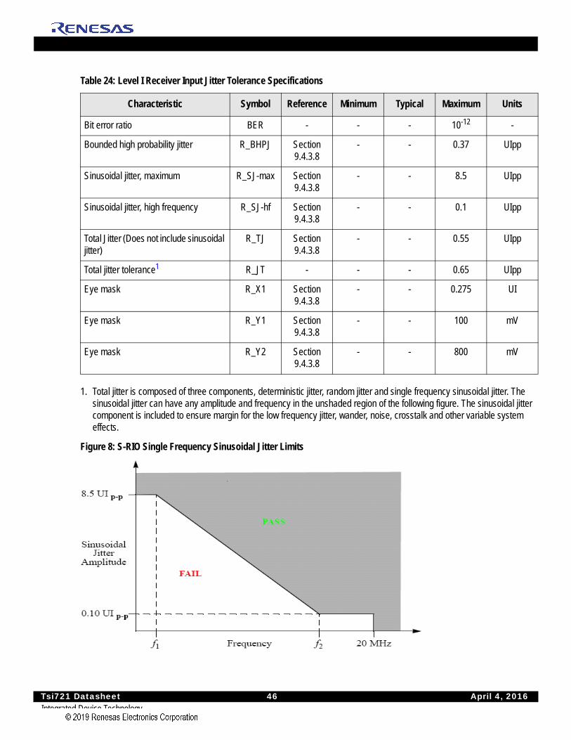
Tsi721 Datasheet 46 April 4, 2016Integrated Device Technology
1. Total jitter is composed of three components, deterministic jitter, random jitter and single frequency sinusoidal jitter. The sinusoidal jitter can have any amplitude and frequency in the unshaded region of the following figure. The sinusoidal jitter component is included to ensure margin for the low frequency jitter, wander, noise, crosstalk and other variable system effects.
Figure 8: S-RIO Single Frequency Sinusoidal Jitter Limits
Table 24: Level I Receiver Input Jitter Tolerance Specifications
Characteristic Symbol Reference Minimum Typical Maximum Units
Bit error ratio BER - - - 10-12 -
Bounded high probability jitter R_BHPJ Section 9.4.3.8
- - 0.37 UIpp
Sinusoidal jitter, maximum R_SJ-max Section 9.4.3.8
- - 8.5 UIpp
Sinusoidal jitter, high frequency R_SJ-hf Section 9.4.3.8
- - 0.1 UIpp
Total Jitter (Does not include sinusoidal jitter)
R_TJ Section 9.4.3.8
- - 0.55 UIpp
Total jitter tolerance1 R_JT - - - 0.65 UIpp
Eye mask R_X1 Section 9.4.3.8
- - 0.275 UI
Eye mask R_Y1 Section 9.4.3.8
- - 100 mV
Eye mask R_Y2 Section 9.4.3.8
- - 800 mV
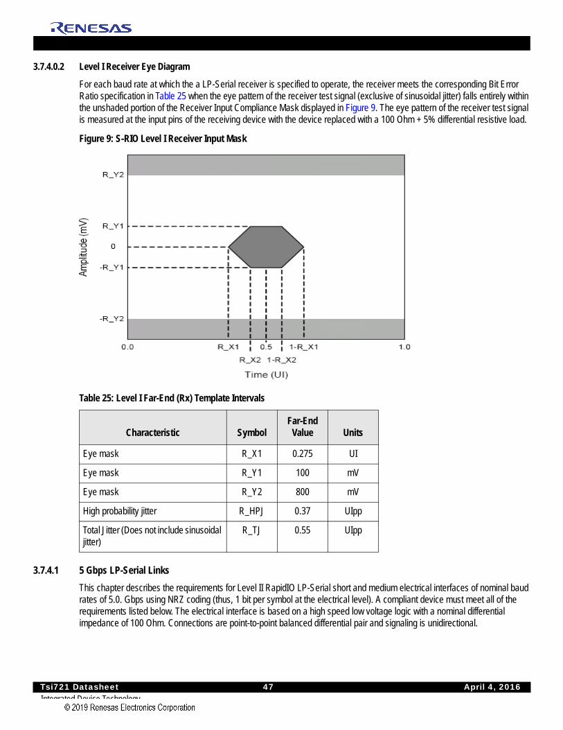
Tsi721 Datasheet 47 April 4, 2016Integrated Device Technology
3.7.4.0.2 Level I Receiver Eye Diagram
For each baud rate at which the a LP-Serial receiver is specified to operate, the receiver meets the corresponding Bit Error Ratio specification in Table 25 when the eye pattern of the receiver test signal (exclusive of sinusoidal jitter) falls entirely within the unshaded portion of the Receiver Input Compliance Mask displayed in Figure 9. The eye pattern of the receiver test signal is measured at the input pins of the receiving device with the device replaced with a 100 Ohm + 5% differential resistive load.
Figure 9: S-RIO Level I Receiver Input Mask
3.7.4.1 5 Gbps LP-Serial Links
This chapter describes the requirements for Level II RapidIO LP-Serial short and medium electrical interfaces of nominal baud rates of 5.0. Gbps using NRZ coding (thus, 1 bit per symbol at the electrical level). A compliant device must meet all of the requirements listed below. The electrical interface is based on a high speed low voltage logic with a nominal differential impedance of 100 Ohm. Connections are point-to-point balanced differential pair and signaling is unidirectional.
Table 25: Level I Far-End (Rx) Template Intervals
Characteristic SymbolFar-End
Value Units
Eye mask R_X1 0.275 UI
Eye mask R_Y1 100 mV
Eye mask R_Y2 800 mV
High probability jitter R_HPJ 0.37 UIpp
Total Jitter (Does not include sinusoidal jitter)
R_TJ 0.55 UIpp
Tsi721 Datasheet 48 April 4, 2016Integrated Device Technology
3.7.4.2 Explanatory Note on Level II Transmitter and Receiver Specifications
AC electrical specifications are provided for transmitters and receivers. The parameters for the AC electrical specifications are guided by the OIF CEI Electrical and Jitter Inter-operability agreement for CEI-6G-SR and CEI-6G-LR.
OIF CEI-6G-SR and CEI-6G-LR have similar application goals to S-RIO, as described in Section 10.1, “Level II Application Goals.” The goal of this standard is that electrical designs for S-RIO can reuse electrical designs for OIF CEI-6G, suitably modified for applications at the baud intervals and runs described herein.
3.7.4.3 Level II Electrical Specifications
The electrical interface is based on high speed, low voltage logic with nominal differential impedance of 100 Ohm. Connections are point-to-point balanced differential pair and signaling is unidirectional.
3.7.4.3.1 Level II Transmitter Characteristics
Level II LP-Serial transmitter electrical and timing specifications are stated in the text and tables of this section.
The differential return loss must be better than A0 from f0 to f1 and better than
A0 + Slope*log10(f/f1)
Where f is the frequency from f1 to f2 (see section 8.5.11, Figure 8-12 of the RapidIO Specification (Rev. 2.1). Differential return loss is measured at compliance points T and R. If AC coupling is used, then all components (internal or external) are to be included in this requirement. The reference impedance for the differential return loss measurements is 100 Ohm.
Common mode return loss measurement must be better than -6dB between a minimum frequency of 100 MHz and a maximum frequency of 0.75 times the baud rate. The reference impedance for the common mode return loss is 25 Ohm.
The Tsi721 satisfies the specification requirement that the 20%-80% rise/fall time of the transmitter, as measured at the transmitter output, in each case has a minimum value 30 ps.
Similarly, the timing skew at the output of an LP-Serial transmitter between the two signals that comprise a differential pair does not exceed 10 ps at 5.0.
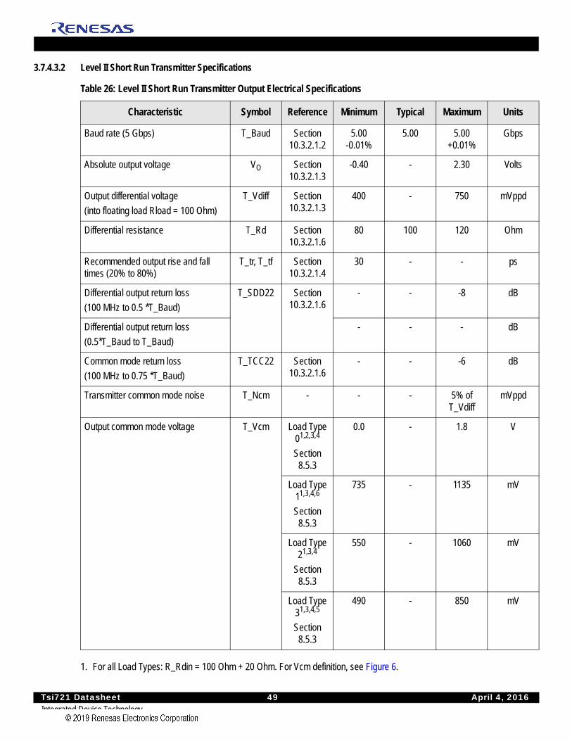
Tsi721 Datasheet 49 April 4, 2016Integrated Device Technology
3.7.4.3.2 Level II Short Run Transmitter Specifications
1. For all Load Types: R_Rdin = 100 Ohm + 20 Ohm. For Vcm definition, see Figure 6.
Table 26: Level II Short Run Transmitter Output Electrical Specifications
Characteristic Symbol Reference Minimum Typical Maximum Units
Baud rate (5 Gbps) T_Baud Section 10.3.2.1.2
5.00 -0.01%
5.00 5.00 +0.01%
Gbps
Absolute output voltage VO Section 10.3.2.1.3
-0.40 - 2.30 Volts
Output differential voltage
(into floating load Rload = 100 Ohm)
T_Vdiff Section 10.3.2.1.3
400 - 750 mVppd
Differential resistance T_Rd Section 10.3.2.1.6
80 100 120 Ohm
Recommended output rise and fall times (20% to 80%)
T_tr, T_tf Section 10.3.2.1.4
30 - - ps
Differential output return loss
(100 MHz to 0.5 *T_Baud)
T_SDD22 Section 10.3.2.1.6
- - -8 dB
Differential output return loss
(0.5*T_Baud to T_Baud)
- - - dB
Common mode return loss
(100 MHz to 0.75 *T_Baud)
T_TCC22 Section 10.3.2.1.6
- - -6 dB
Transmitter common mode noise T_Ncm - - - 5% of T_Vdiff
mVppd
Output common mode voltage T_Vcm Load Type 01,2,3,4
Section 8.5.3
0.0 - 1.8 V
Load Type 11,3,4,6
Section 8.5.3
735 - 1135 mV
Load Type 21,3,4
Section 8.5.3
550 - 1060 mV
Load Type 31,3,4,5
Section 8.5.3
490 - 850 mV
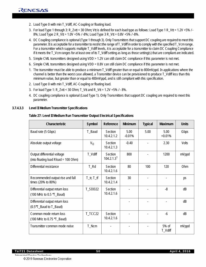
Tsi721 Datasheet 50 April 4, 2016Integrated Device Technology
2. Load Type 0 with min T_Vdiff, AC-Coupling or floating load.
3. For load Type 1 through 3: R_Zvtt < 30 Ohm; Vtt is defined for each load type as follows: Load Type 1 R_Vtt = 1.2V +5% / - 8%; Load Type 2 R_Vtt = 1.0V +5% / -8%; Load Type 3 R_Vtt = 0.8V +5% / -8%.
4. DC Coupling compliance is optional (Type 1 through 3). Only Transmitters that support DC coupling are required to meet this parameter. It is acceptable for a transmitter to restrict the range of T_Vdiff in order to comply with the specified T_Vcm range. For a transmitter which supports multiple T_Vdiff levels, it is acceptable for a transmitter to claim DC Coupling Compliance if it meets the T_Vcm ranges for at least one of its T_Vdiff setting as long as those setting(s) that are compliant are indicated.
5. Simple CML transmitters designed using VDD > 1.2V can still claim DC compliance if this parameter is not met.
6. Simple CML transmitters designed using VDD < 0.8V can still claim DC compliance if this parameter is not met.
1. The transmitter must be able to produce a minimum T_Vdiff greater than or equal to 800mVppd. In applications where the channel is better than the worst case allowed, a Transmitter device can be provisioned to produce T_Vdiff less than this minimum value, but greater than or equal to 400mVppd, and is still compliant with this specification.
2. Load Type 0 with min T_Vdiff, AC-Coupling or floating load.
3. For load Type 1: R_Zvtt < 30 Ohm; T_Vtt and R_Vtt = 1.2V +5% / - 8%.
4. DC coupling compliance is optional (Load Type 1). Only Transmitters that support DC coupling are required to meet this parameter.
3.7.4.3.3 Level II Medium Transmitter Specifications
Table 27: Level II Medium Run Transmitter Output Electrical Specifications
Characteristic Symbol Reference Minimum Typical Maximum Units
Baud rate (5 Gbps) T_Baud Section 10.4.2.1.2
5.00 -0.01%
5.00 5.00 +0.01%
Gbps
Absolute output voltage VO Section 10.4.2.1.3
-0.40 - 2.30 Volts
Output differential voltage
(into floating load Rload = 100 Ohm)
T_Vdiff Section 104.2.1.31
800 - 1200 mVppd
Differential resistance T_Rd Section 10.4.2.1.6
80 100 120 Ohm
Recommended output rise and fall times (20% to 80%)
T_tr, T_tf Section 10.4.2.1.4
30 - - ps
Differential output return loss
(100 MHz to 0.5 *T_Baud)
T_SDD22 Section 10.4.2.1.6
- - -8 dB
Differential output return loss
(0.5*T_Baud to T_Baud)
- - - dB
Common mode return loss
(100 MHz to 0.75 *T_Baud)
T_TCC22 Section 10.4.2.1.6
- - -6 dB
Transmitter common mode noise T_Ncm - - - 5% of T_Vdiff
mVppd
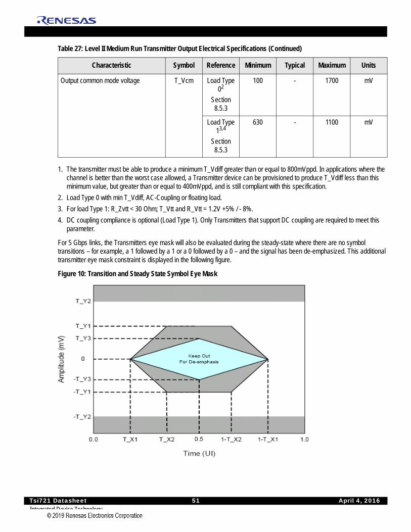
Tsi721 Datasheet 51 April 4, 2016Integrated Device Technology
1. The transmitter must be able to produce a minimum T_Vdiff greater than or equal to 800mVppd. In applications where the channel is better than the worst case allowed, a Transmitter device can be provisioned to produce T_Vdiff less than this minimum value, but greater than or equal to 400mVppd, and is still compliant with this specification.
2. Load Type 0 with min T_Vdiff, AC-Coupling or floating load.
3. For load Type 1: R_Zvtt < 30 Ohm; T_Vtt and R_Vtt = 1.2V +5% / - 8%.
4. DC coupling compliance is optional (Load Type 1). Only Transmitters that support DC coupling are required to meet this parameter.
For 5 Gbps links, the Transmitters eye mask will also be evaluated during the steady-state where there are no symbol transitions – for example, a 1 followed by a 1 or a 0 followed by a 0 – and the signal has been de-emphasized. This additional transmitter eye mask constraint is displayed in the following figure.
Figure 10: Transition and Steady State Symbol Eye Mask
Output common mode voltage T_Vcm Load Type 02
Section 8.5.3
100 - 1700 mV
Load Type 13,4
Section 8.5.3
630 - 1100 mV
Table 27: Level II Medium Run Transmitter Output Electrical Specifications (Continued)
Characteristic Symbol Reference Minimum Typical Maximum Units

Tsi721 Datasheet 52 April 4, 2016Integrated Device Technology
During the steady-state, the eye mask prevents the transmitter from de-emphasizing the low frequency content of the data too much and limiting the available signal-to-noise at the receiver. The de-emphasis introduces a jitter artifact that is not accounted for in this eye mask. This additional jitter is caused by the finite rise/fall time of the transmitter and the non-uniform voltage swing between the transitions. This additional deterministic jitter must be accounted for as part of the high probability jitter and is specified in the following table.
Table 28: Level II Medium Run Near-End (Tx) Template Intervals
Characteristic Symbol Near-End MRValue Comments Units
Eye mask T_X1 0.15 - UI
Eye mask T_X2 0.40 - UI
Eye mask T_Y1 200 For connection to short run Rx
mV
400 For connection to long run Rx
Eye mask T_Y2 375 For connection to short run Rx
mV
600 For connection to long run Rx
Eye mask T_Y3 N/A - mV
Uncorrelated bounded high probability jitter
T_UBHPJ 0.15 - UIpp
Duty cycle distortion T_DCD 0.05 - UIpp
Total jitter T_TJ 0.30 - UIpp
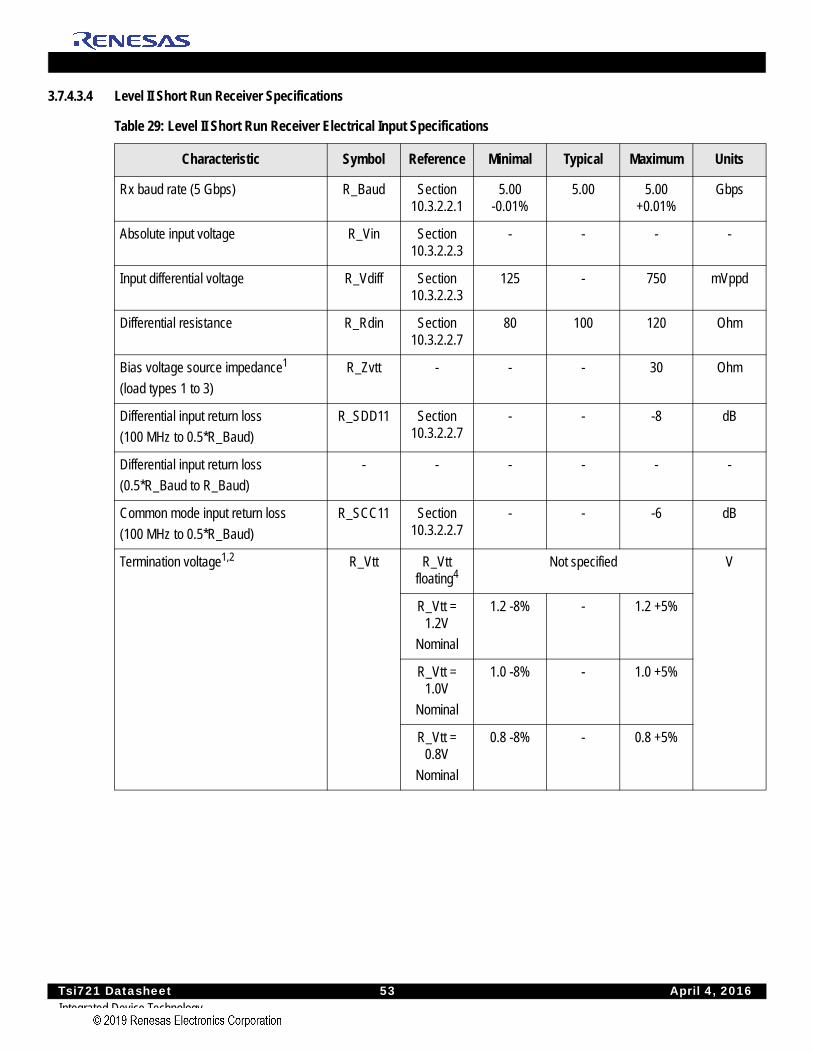
Tsi721 Datasheet 53 April 4, 2016Integrated Device Technology
3.7.4.3.4 Level II Short Run Receiver Specifications
Table 29: Level II Short Run Receiver Electrical Input Specifications
Characteristic Symbol Reference Minimal Typical Maximum Units
Rx baud rate (5 Gbps) R_Baud Section 10.3.2.2.1
5.00 -0.01%
5.00 5.00 +0.01%
Gbps
Absolute input voltage R_Vin Section 10.3.2.2.3
- - - -
Input differential voltage R_Vdiff Section 10.3.2.2.3
125 - 750 mVppd
Differential resistance R_Rdin Section 10.3.2.2.7
80 100 120 Ohm
Bias voltage source impedance1
(load types 1 to 3)
R_Zvtt - - - 30 Ohm
Differential input return loss
(100 MHz to 0.5*R_Baud)
R_SDD11 Section 10.3.2.2.7
- - -8 dB
Differential input return loss
(0.5*R_Baud to R_Baud)
- - - - - -
Common mode input return loss
(100 MHz to 0.5*R_Baud)
R_SCC11 Section 10.3.2.2.7
- - -6 dB
Termination voltage1,2 R_Vtt R_Vtt floating4
Not specified V
R_Vtt = 1.2V
Nominal
1.2 -8% - 1.2 +5%
R_Vtt = 1.0V
Nominal
1.0 -8% - 1.0 +5%
R_Vtt = 0.8V
Nominal
0.8 -8% - 0.8 +5%
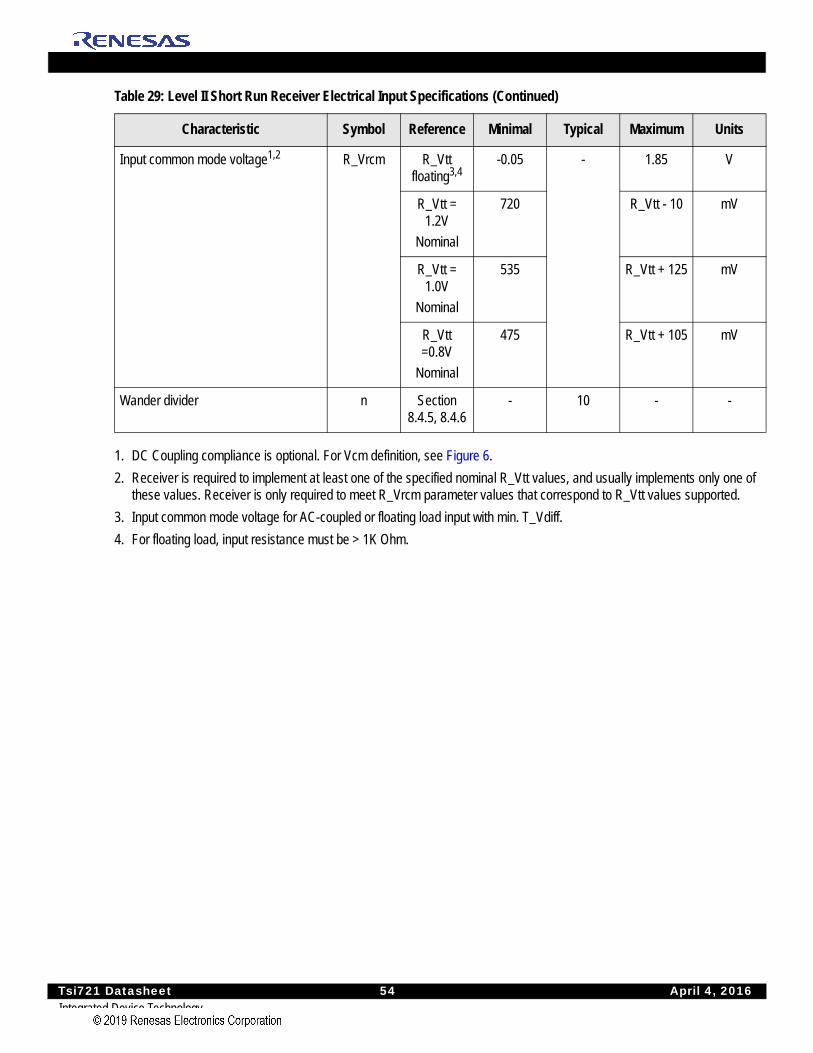
Tsi721 Datasheet 54 April 4, 2016Integrated Device Technology
1. DC Coupling compliance is optional. For Vcm definition, see Figure 6.
2. Receiver is required to implement at least one of the specified nominal R_Vtt values, and usually implements only one of these values. Receiver is only required to meet R_Vrcm parameter values that correspond to R_Vtt values supported.
3. Input common mode voltage for AC-coupled or floating load input with min. T_Vdiff.
4. For floating load, input resistance must be > 1K Ohm.
Input common mode voltage1,2 R_Vrcm R_Vtt floating3,4
-0.05 - 1.85 V
R_Vtt = 1.2V
Nominal
720 R_Vtt - 10 mV
R_Vtt = 1.0V
Nominal
535 R_Vtt + 125 mV
R_Vtt =0.8V
Nominal
475 R_Vtt + 105 mV
Wander divider n Section 8.4.5, 8.4.6
- 10 - -
Table 29: Level II Short Run Receiver Electrical Input Specifications (Continued)
Characteristic Symbol Reference Minimal Typical Maximum Units
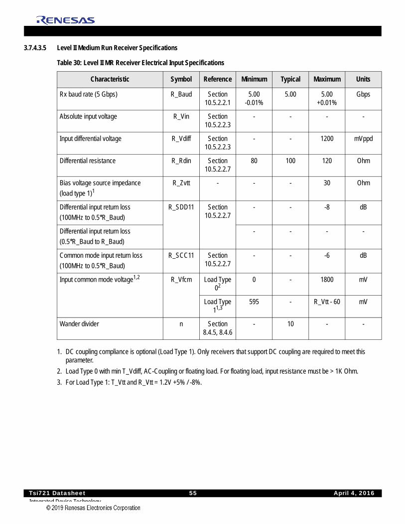
Tsi721 Datasheet 55 April 4, 2016Integrated Device Technology
3.7.4.3.5 Level II Medium Run Receiver Specifications
1. DC coupling compliance is optional (Load Type 1). Only receivers that support DC coupling are required to meet this parameter.
2. Load Type 0 with min T_Vdiff, AC-Coupling or floating load. For floating load, input resistance must be > 1K Ohm.
3. For Load Type 1: T_Vtt and R_Vtt = 1.2V +5% / -8%.
Table 30: Level II MR Receiver Electrical Input Specifications
Characteristic Symbol Reference Minimum Typical Maximum Units
Rx baud rate (5 Gbps) R_Baud Section 10.5.2.2.1
5.00 -0.01%
5.00 5.00 +0.01%
Gbps
Absolute input voltage R_Vin Section 10.5.2.2.3
- - - -
Input differential voltage R_Vdiff Section 10.5.2.2.3
- - 1200 mVppd
Differential resistance R_Rdin Section 10.5.2.2.7
80 100 120 Ohm
Bias voltage source impedance
(load type 1)1R_Zvtt - - - 30 Ohm
Differential input return loss
(100MHz to 0.5*R_Baud)
R_SDD11 Section 10.5.2.2.7
- - -8 dB
Differential input return loss
(0.5*R_Baud to R_Baud)
- - - -
Common mode input return loss
(100MHz to 0.5*R_Baud)
R_SCC11 Section 10.5.2.2.7
- - -6 dB
Input common mode voltage1,2 R_Vfcm Load Type 02
0 - 1800 mV
Load Type 11,3
595 - R_Vtt - 60 mV
Wander divider n Section 8.4.5, 8.4.6
- 10 - -
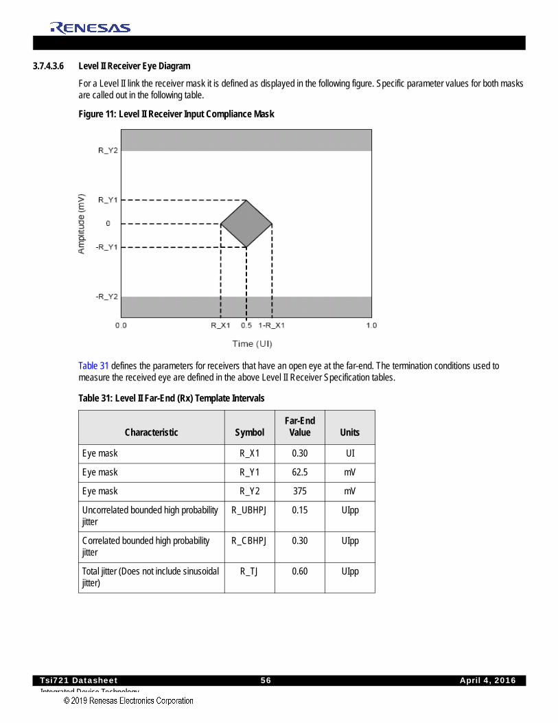
Tsi721 Datasheet 56 April 4, 2016Integrated Device Technology
3.7.4.3.6 Level II Receiver Eye Diagram
For a Level II link the receiver mask it is defined as displayed in the following figure. Specific parameter values for both masks are called out in the following table.
Figure 11: Level II Receiver Input Compliance Mask
Table 31 defines the parameters for receivers that have an open eye at the far-end. The termination conditions used to measure the received eye are defined in the above Level II Receiver Specification tables.
Table 31: Level II Far-End (Rx) Template Intervals
Characteristic SymbolFar-End
Value Units
Eye mask R_X1 0.30 UI
Eye mask R_Y1 62.5 mV
Eye mask R_Y2 375 mV
Uncorrelated bounded high probability jitter
R_UBHPJ 0.15 UIpp
Correlated bounded high probability jitter
R_CBHPJ 0.30 UIpp
Total jitter (Does not include sinusoidal jitter)
R_TJ 0.60 UIpp
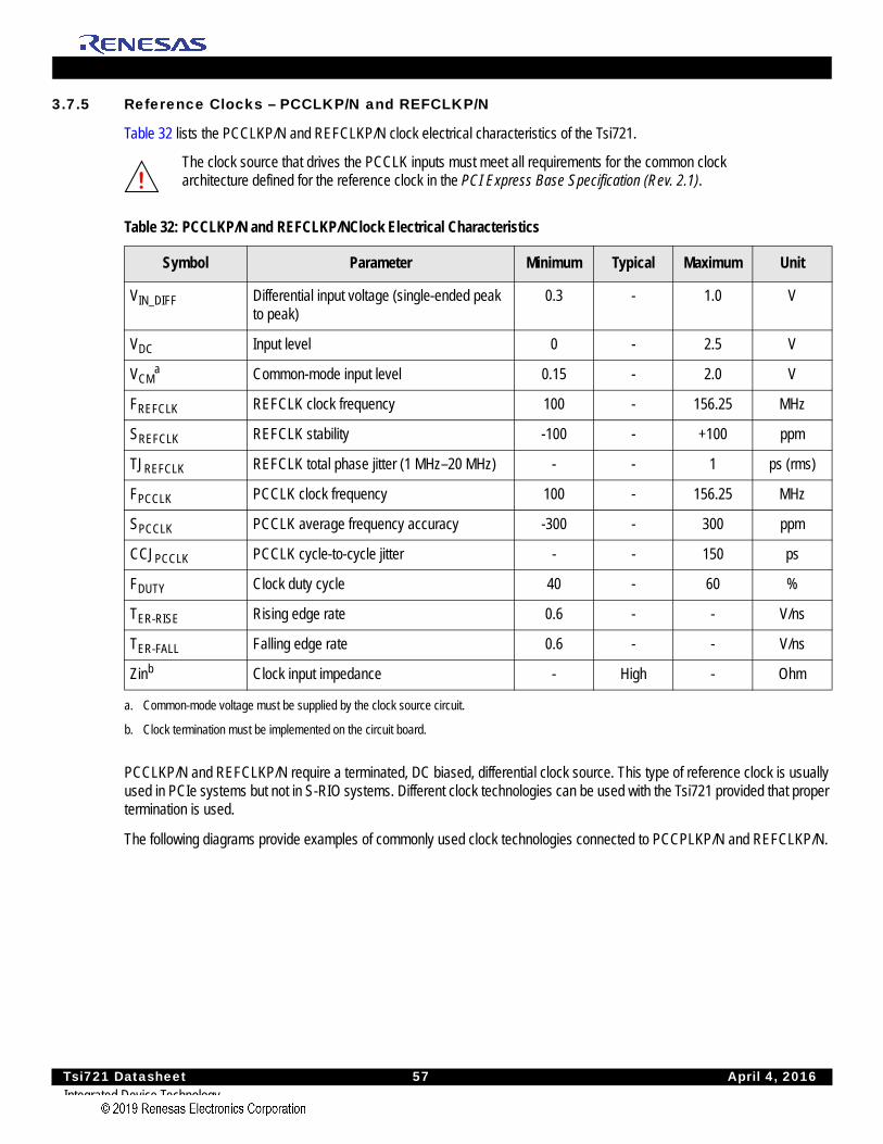
Tsi721 Datasheet 57 April 4, 2016Integrated Device Technology
3.7.5 Reference Clocks – PCCLKP/N and REFCLKP/N
Table 32 lists the PCCLKP/N and REFCLKP/N clock electrical characteristics of the Tsi721.
PCCLKP/N and REFCLKP/N require a terminated, DC biased, differential clock source. This type of reference clock is usually used in PCIe systems but not in S-RIO systems. Different clock technologies can be used with the Tsi721 provided that proper termination is used.
The following diagrams provide examples of commonly used clock technologies connected to PCCPLKP/N and REFCLKP/N.
The clock source that drives the PCCLK inputs must meet all requirements for the common clock architecture defined for the reference clock in the PCI Express Base Specification (Rev. 2.1).
Table 32: PCCLKP/N and REFCLKP/NClock Electrical Characteristics
Symbol Parameter Minimum Typical Maximum Unit
VIN_DIFF Differential input voltage (single-ended peak to peak)
0.3 - 1.0 V
VDC Input level 0 - 2.5 V
VCMa
a. Common-mode voltage must be supplied by the clock source circuit.
Common-mode input level 0.15 - 2.0 V
FREFCLK REFCLK clock frequency 100 - 156.25 MHz
SREFCLK REFCLK stability -100 - +100 ppm
TJREFCLK REFCLK total phase jitter (1 MHz–20 MHz) - - 1 ps (rms)
FPCCLK PCCLK clock frequency 100 - 156.25 MHz
SPCCLK PCCLK average frequency accuracy -300 - 300 ppm
CCJPCCLK PCCLK cycle-to-cycle jitter - - 150 ps
FDUTY Clock duty cycle 40 - 60 %
TER-RISE Rising edge rate 0.6 - - V/ns
TER-FALL Falling edge rate 0.6 - - V/ns
Zinb
b. Clock termination must be implemented on the circuit board.
Clock input impedance - High - Ohm
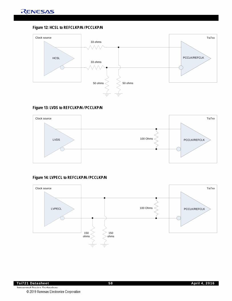
Tsi721 Datasheet 58 April 4, 2016Integrated Device Technology
Figure 12: HCSL to REFCLKP/N / PCCLKP/N
Figure 13: LVDS to REFCLKP/N / PCCLKP/N
Figure 14: LVPECL to REFCLKP/N / PCCLKP/N
33 ohms
33 ohms
50 ohms 50 ohms
PCCLK/REFCLKHCSL
Tsi7xxClock source
PCCLK/REFCLKLVDS 100 Ohms
Clock source Tsi7xx
PCCLK/REFCLKLVPECL
150ohms
150ohms
100 Ohms
Tsi7xxClock source
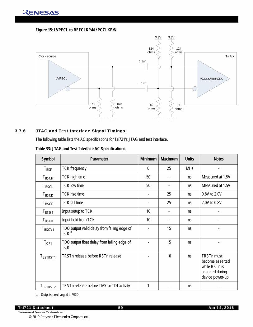
Tsi721 Datasheet 59 April 4, 2016Integrated Device Technology
Figure 15: LVPECL to REFCLKP/N / PCCLKP/N
3.7.6 JTAG and Test Interface Signal Timings
The following table lists the AC specifications for Tsi721’s JTAG and test interface.
Table 33: JTAG and Test Interface AC Specifications
Symbol Parameter Minimum Maximum Units Notes
TBSF TCK frequency 0 25 MHz -
TBSCH TCK high time 50 - ns Measured at 1.5V
TBSCL TCK low time 50 - ns Measured at 1.5V
TBSCR TCK rise time - 25 ns 0.8V to 2.0V
TBSCF TCK fall time - 25 ns 2.0V to 0.8V
TBSIS1 Input setup to TCK 10 - ns -
TBSIH1 Input hold from TCK 10 - ns -
TBSOV1 TDO output valid delay from falling edge of TCK.a
a. Outputs precharged to VDD.
- 15 ns -
TOF1 TDO output float delay from falling edge of TCK
- 15 ns -
TBSTRST1 TRSTn release before RSTn release - 10 ns TRSTn must become asserted while RSTn is asserted during device power-up
TBSTRST2 TRSTn release before TMS or TDI activity 1 - ns -
PCCLK/REFCLKLVPECL
150ohms
150ohms
Clock source
82ohms
3.3V 3.3V
124ohms
124ohms
82ohms
0.1uf
0.1uf
Tsi7xx
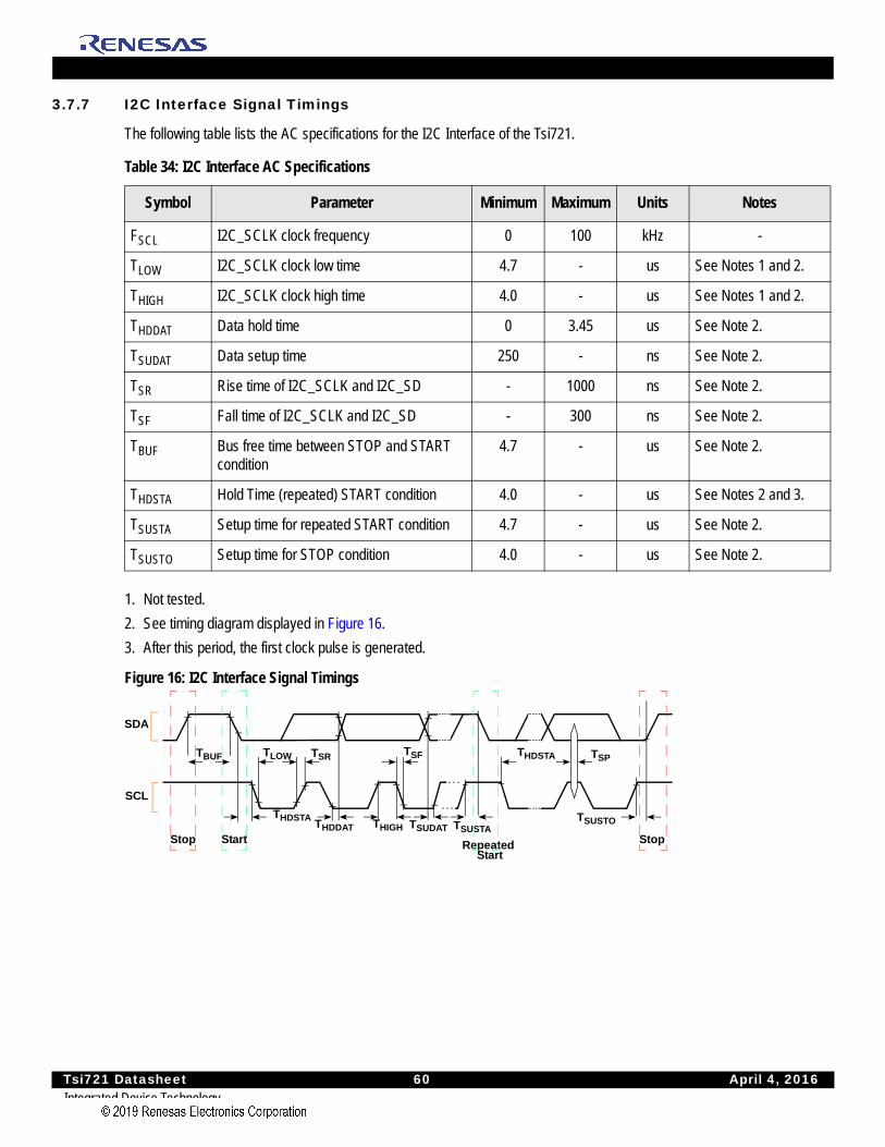
Tsi721 Datasheet 60 April 4, 2016Integrated Device Technology
3.7.7 I2C Interface Signal Timings
The following table lists the AC specifications for the I2C Interface of the Tsi721.
1. Not tested.
2. See timing diagram displayed in Figure 16.
3. After this period, the first clock pulse is generated.
Figure 16: I2C Interface Signal Timings
Table 34: I2C Interface AC Specifications
Symbol Parameter Minimum Maximum Units Notes
FSCL I2C_SCLK clock frequency 0 100 kHz -
TLOW I2C_SCLK clock low time 4.7 - us See Notes 1 and 2.
THIGH I2C_SCLK clock high time 4.0 - us See Notes 1 and 2.
THDDAT Data hold time 0 3.45 us See Note 2.
TSUDAT Data setup time 250 - ns See Note 2.
TSR Rise time of I2C_SCLK and I2C_SD - 1000 ns See Note 2.
TSF Fall time of I2C_SCLK and I2C_SD - 300 ns See Note 2.
TBUF Bus free time between STOP and START condition
4.7 - us See Note 2.
THDSTA Hold Time (repeated) START condition 4.0 - us See Notes 2 and 3.
TSUSTA Setup time for repeated START condition 4.7 - us See Note 2.
TSUSTO Setup time for STOP condition 4.0 - us See Note 2.
SDA
SCL
TBUF
Stop Start
TLOW
THDSTATHIGH
TSR
THDDAT
TSF
TSUDAT TSUSTA
Repeated
THDSTA TSP
Stop
TSUSTO
Start
Tsi721 Datasheet 61 April 4, 2016Integrated Device Technology
3.7.8 GPIO Interface Signal Timings
The following table lists the AC specifications for the GPIO Interface of the Tsi721.
3.7.9 RSTn Signal Timings
The following table lists the RSTn signal timing for the Tsi721 (see PCIe spec 2.1 section 6.6.1 and CEM 2.0 table 2.6.2).
Table 35: GPIO Interface AC Specifications
Symbol Parameter Minimum Maximum Units Notes
TMIN-HIGH Minimum signal high time 50 - ns -
TMIN-LOW Minimum signal low time 50 - ns -
Table 36: RSTn Signal AC Specifications
Symbol Parameter Minimum Maximum Units Notes
Tperst When asserted, RSTn must remain asserted at least this long
100 - us -
Tfail When power become invalid, RSTn must be asserted within this time
- 500 ns -
Tperst-clk RSTn must remain asserted after any supplied reference clock (REFCLK and PCCLK) is stable
100 - us -
Tsi721 Datasheet 62 April 4, 2016Integrated Device Technology
4. Package SpecificationsTopics discussed include the following:
• Package Dimensions
• Package Diagrams
• Thermal Characteristics
• Moisture Sensitivity
4.1 Package Dimensions
Table 37: Package Dimensions
Specification Description
Package type FCBGA
Package size 13 x 13 mm
Ball pitch 1 mm
Ball count 143
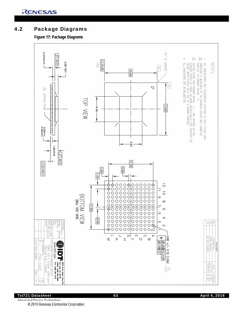
Tsi721 Datasheet 63 April 4, 2016Integrated Device Technology
4.2 Package DiagramsFigure 17: Package Diagrams
Tsi721 Datasheet 64 April 4, 2016Integrated Device Technology
4.3 Thermal CharacteristicsHeat generated by the packaged silicon must be removed from the package to ensure the silicon is maintained within its functional and maximum design temperature limits. If heat buildup becomes excessive, the silicon temperature may exceed the temperature limits. A consequence of this is that the silicon may fail to meet the performance specifications and the reliability objectives may be affected.
Failure mechanisms and failure rate of a device has an exponential dependence on the silicon operating temperatures. Therefore, the control of the package, and by extension the junction temperature, is essential to ensure product reliability. The Tsi721 is specified safe for operation when the junction temperature is within the recommended limits as displayed in Table 12.
Table 38 shows the simulated thermal characteristic (Theta JB and Theta JC) of the Tsi721 package.
Table 39 shows the simulated junction to ambient characteristics of the Tsi721. The thermal resistance Theta JA characteristics of a package depends on multiple variables other than just the package. In a typical application, designers must consider various system-level and environmental characteristics, such as:
• Package mounting (vertical/horizontal)
• System airflow conditions (laminar/turbulent)
• Heat sink design and thermal characteristics
• Heat sink attachment method
• PWB size, layer count, and conductor thickness
• Influence of the heat dissipating components assembled on the PWB (neighboring effects)
The results in Table 39 are based on a JEDEC Thermal Test Board configuration (JESD51-9), and do not factor in the system-level characteristics described above. As such, these values are for reference only.
4.4 Moisture SensitivityThe moisture sensitivity level (MSL) for the Tsi721 is 4.
Table 38: Junction to Ambient Characteristics – Theta JB/JC
Interface Results (C/W)
Theta JB 8.78
Theta JC 0.11
Table 39: Junction to Ambient Characteristics – Theta JA
Device
Theta JA (C/W)
0 m/s 1 m/s 2 m/s
Tsi721 13.1 12.06 11.4
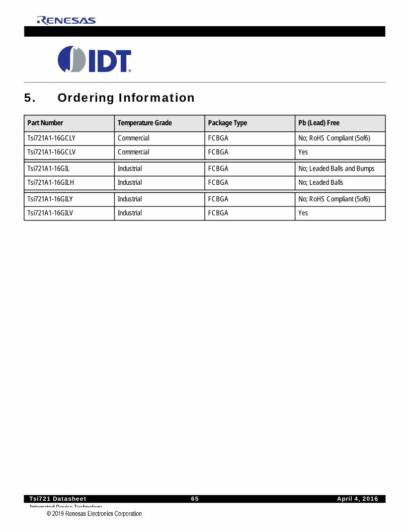
Tsi721 Datasheet 65 April 4, 2016Integrated Device Technology
5. Ordering Information
Part Number Temperature Grade Package Type Pb (Lead) Free
Tsi721A1-16GCLY Commercial FCBGA No; RoHS Compliant (5of6)
Tsi721A1-16GCLV Commercial FCBGA Yes
Tsi721A1-16GIL Industrial FCBGA No; Leaded Balls and Bumps
Tsi721A1-16GILH Industrial FCBGA No; Leaded Balls
Tsi721A1-16GILY Industrial FCBGA No; RoHS Compliant (5of6)
Tsi721A1-16GILV Industrial FCBGA Yes

DISCLAIMER Integrated Device Technology, Inc. (IDT) reserves the right to modify the products and/or specifications described herein at any time, without notice, at IDT's sole discretion. Performance spec-ifications and operating parameters of the described products are determined in an independent state and are not guaranteed to perform the same way when installed in customer products. The informationcontained herein is provided without representation or warranty of any kind, whether express or implied, including, but not limited to, the suitability of IDT's products for any particular purpose, an impliedwarranty of merchantability, or non-infringement of the intellectual property rights of others. This document is presented only as a guide and does not convey any license under intellectual property rights ofIDT or any third parties.
IDT's products are not intended for use in applications involving extreme environmental conditions or in life support systems or similar devices where the failure or malfunction of an IDT product can be rea-sonably expected to significantly affect the health or safety of users. Anyone using an IDT product in such a manner does so at their own risk, absent an express, written agreement by IDT.
Integrated Device Technology, IDT and the IDT logo are trademarks or registered trademarks of IDT and its subsidiaries in the United States and other countries. Other trademarks used herein are the propertyof IDT or their respective third party owners. For a glossary of common terms, visit www.idt.com/go/glossary. Integrated Device Technology. All rights reserved.
Tech Supportwww.idt.com/go/support
Sales1-800-345-7015 or 408-284-8200 Fax: 408-284-2775www.IDT.com/go/sales
Corporate Headquarters6024 Silver Creek Valley Road San Jose, CA 95138 USAwww.IDT.com
Tsi721 Datasheet 66 April 4, 2016Integrated Device Technology
Corporate HeadquartersTOYOSU FORESIA, 3-2-24 Toyosu,Koto-ku, Tokyo 135-0061, Japanwww.renesas.com
Contact InformationFor further information on a product, technology, the most up-to-date version of a document, or your nearest sales office, please visit:www.renesas.com/contact/
TrademarksRenesas and the Renesas logo are trademarks of Renesas Electronics Corporation. All trademarks and registered trademarks are the property of their respective owners.
IMPORTANT NOTICE AND DISCLAIMER
RENESAS ELECTRONICS CORPORATION AND ITS SUBSIDIARIES (“RENESAS”) PROVIDES TECHNICAL SPECIFICATIONS AND RELIABILITY DATA (INCLUDING DATASHEETS), DESIGN RESOURCES (INCLUDING REFERENCE DESIGNS), APPLICATION OR OTHER DESIGN ADVICE, WEB TOOLS, SAFETY INFORMATION, AND OTHER RESOURCES “AS IS” AND WITH ALL FAULTS, AND DISCLAIMS ALL WARRANTIES, EXPRESS OR IMPLIED, INCLUDING, WITHOUT LIMITATION, ANY IMPLIED WARRANTIES OF MERCHANTABILITY, FITNESS FOR A PARTICULAR PURPOSE, OR NON-INFRINGEMENT OF THIRD PARTY INTELLECTUAL PROPERTY RIGHTS.
These resources are intended for developers skilled in the art designing with Renesas products. You are solely responsible for (1) selecting the appropriate products for your application, (2) designing, validating, and testing your application, and (3) ensuring your application meets applicable standards, and any other safety, security, or other requirements. These resources are subject to change without notice. Renesas grants you permission to use these resources only for development of an application that uses Renesas products. Other reproduction or use of these resources is strictly prohibited. No license is granted to any other Renesas intellectual property or to any third party intellectual property. Renesas disclaims responsibility for, and you will fully indemnify Renesas and its representatives against, any claims, damages, costs, losses, or liabilities arising out of your use of these resources. Renesas' products are provided only subject to Renesas' Terms and Conditions of Sale or other applicable terms agreed to in writing. No use of any Renesas resources expands or otherwise alters any applicable warranties or warranty disclaimers for these products.
(Rev.1.0 Mar 2020)
© 2020 Renesas Electronics Corporation. All rights reserved.