Embed Size (px)
Citation preview
FN6924Rev 3.00
June 16, 2011
ISL62881, ISL62881BSingle-Phase PWM Regulator for IMVP-6.5™ Mobile CPUs and GPUs
DATASHEET
The ISL62881 is a single-phase PWM buck regulator for miroprocessor or graphics processor core power supply. It uses an integrated gate driver to provide a complete solution. The PWM modulator of ISL62881 is based on Intersil's Robust Ripple Regulator (R3) technology™. Compared with traditional modulators, the R3™ modulator commands variable switching frequency during load transients, achieving faster transient response. With the same modulator, the switching frequency is reduced at light load, increasing the regulator efficiency.
The ISL62881 can be configured as CPU or graphics Vcore controller and is fully compliant with IMVP-6.5™ specifications. It responds to DPRSLPVR signals by entering/exiting diode emulation mode. It reports the regulator output current through the IMON pin. It senses the current by using either discrete resistor or inductor DCR whose variation over-temperature can be thermally compensated by a single NTC thermistor. It uses differential remote voltage sensing to accurately regulate the processor die voltage. The adaptive body diode conduction time reduction function minimizes the body diode conduction loss in diode emulation mode. User-selectable overshoot reduction function offers an option to aggressively reduce the output capacitors as well as the option to disable it for users concerned about increased system thermal stress.
Maintaining all the ISL62881 functions, the ISL62881B offers VR_TT# function for thermal throttling control. It also offers the split LGATE function to further improve light load efficiency.
Features• Precision Core Voltage Regulation
- 0.5% System Accuracy Over-Temperature
- Enhanced Load Line Accuracy
• Voltage Identification Input
- 7-Bit VID Input, 0V to 1.500V in 12.5mV Steps
- Supports VID Changes On-The-Fly
• Supports Multiple Current Sensing Methods
- Lossless Inductor DCR Current Sensing
- Precision Resistor Current Sensing
• Superior Noise Immunity and Transient Response
• Current Monitor
• Differential Remote Voltage Sensing
• High Efficiency Across Entire Load Range
• Integrated Gate Driver
• Split LGATE Driver to Increase Light-Load Efficiency (for ISL62881B)
• Adaptive Body Diode Conduction Time Reduction
• User-selectable Overshoot Reduction Function
• Capable of Disabling the Droop Function
• Audio-filtering for GPU Application
• Small Footprint 28 Ld 4x4 TQFN Package
• Pb-Free (RoHS Compliant)
Applications• Notebook Computers
Ordering InformationPART NUMBER(Notes 1, 2, 3)
PART MARKING
TEMP. RANGE(°C)
PACKAGE(Pb-Free)
PKG.DWG. #
ISL62881HRTZ 628 81HRTZ -10 to +100 28 Ld 4x4 TQFN L28.4x4
ISL62881BHRTZ 62881B HRTZ -10 to +100 32 Ld 5x5 TQFN L32.5x5E
NOTES:
1. Add “-T*” suffix for tape and reel. Please refer to TB347 for details on reel specifications.
2. These Intersil Pb-free plastic packaged products employ special Pb-free material sets, molding compounds/die attach materials, and 100% matte tin plate plus anneal (e3 termination finish, which is RoHS compliant and compatible with both SnPb and Pb-free soldering operations). Intersil Pb-free products are MSL classified at Pb-free peak reflow temperatures that meet or exceed the Pb-free requirements of IPC/JEDEC J STD-020.
3. For Moisture Sensitivity Level (MSL), please see device information page for ISL62881, ISL62881B. For more information on MSL please see techbrief TB363.
FN6924 Rev 3.00 Page 1 of 35June 16, 2011
ISL62881, ISL62881B
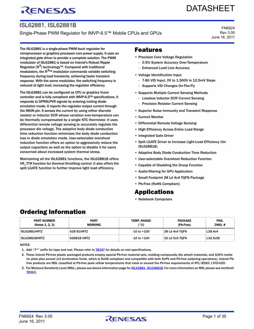
Pin Function Descriptions
GND (Bottom Pad)Signal common of the IC. Unless otherwise stated, signals are referenced to the GND pin.
CLK_EN#Open drain output to enable system PLL clock; goes active 13 switching cycles after Vcore is within 10% of Vboot.
PGOODPower-Good open-drain output indicating when the regulator is able to supply regulated voltage. Pull-up externally with a 680 resistor to VCCP or 1.9k to 3.3V.
RBIASA resistor to GND sets internal current reference. A 147k resistor sets the controller for CPU core application and a 47k resistor sets the controller for GPU core application.
VR_TT#Thermal overload output indicator.
NTCThermistor input to VR_TT# circuit.
VWA resistor from this pin to COMP programs the switching frequency (8k gives approximately 300kHz).
COMPThis pin is the output of the error amplifier. Also, a resistor across this pin and GND adjusts the overcurrent threshold.
FBThis pin is the inverting input of the error amplifier.
VSENRemote core voltage sense input. Connect to microprocessor die.
RTNRemote voltage sensing return. Connect to ground at microprocessor die.
ISUM- and ISUM+Droop current sense input.
VDD5V bias power.
VINBattery supply voltage, used for feed-forward.
IMONAn analog output. IMON outputs a current proportional to the regulator output current.
BOOTConnect an MLCC capacitor across the BOOT and the PHASE pins. The boot capacitor is charged through an internal boot
Pin ConfigurationsISL62881
(28 LD TQFN)TOP VIEW
ISL62881B(32 LD TQFN)
TOP VIEW
1
28
2
3
4
5
6
7
21
20
19
18
17
16
15
27 26 25 24 23 22
8 9 10 11 12 13 14
GND PAD(BOTTOM)
VID
6
VID
4
VID
3
VID
2
VID0
DP
RS
LP
VR
VCCP
LGATE
PHASE
UGATE
COMP
FB
VW
PGOOD
RBIAS
CLK_EN#
VID
5
VR
_ON
VSSP
ISU
M-
ISU
M+
VIN
IMO
N
VD
D
RT
N
VSEN
BO
OT
VID1 1
32
2
3
4
5
6
7
24
23
22
21
20
19
18
31 30 29 28 27 26
9 10 11 12 13 14 15
GND PAD(BOTTOM)
VR
_O
N
VID
5
VID
4
VI D
3
VID0
CLK
_E
N#
VCCP
LGATEa
PHASE
GND
VW
NTC
RBIAS
VR_TT#
VID
6
DP
RS
L PV
R
VSSP
ISU
M-
ISU
M+
VIN
IMO
N
VD
D
VS
EN
VID1
8
COMP
FB
PGOOD
BO
OT
16
RT
N
17 UGATE
LGATEb
25
VID
2
FN6924 Rev 3.00 Page 2 of 35June 16, 2011
ISL62881, ISL62881B
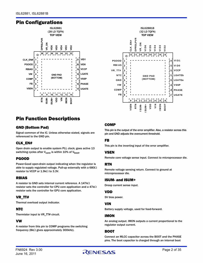
diode connected from the VCCP pin to the BOOT pin, each time the PHASE pin drops below VCCP minus the voltage dropped across the internal boot diode.
UGATEOutput of the high-side MOSFET gate driver. Connect the UGATE pin to the gate of the high-side MOSFET.
PHASECurrent return path for the high-side MOSFET gate driver. Connect the PHASE pin to the node consisting of the high-side MOSFET source, the low-side MOSFET drain and the output inductor.
VSSPCurrent return path for the low-side MOSFET gate driver. Connect the VSSP pin to the source of the low-side MOSFET through a low impedance path, preferably in parallel with the trace connecting the LGATE pin to the gate of the low-side MOSFET.
LGATE (for ISL62881)Output of the low-side MOSFET gate driver. Connect the LGATE pin to the gate of the low-side MOSFET.
LGATEa (for ISL62881B)Output of the low-side MOSFET gate driver that is always active. Connect the LGATEa pin to the gate of the low-side MOSFET that is active all the time.
LGATEb (For ISL62881B)Another output of the low-side MOSFET gate driver. This gate driver will be pulled low when the DPRSLPVR pin logic is high. Connect the LGATEb pin to the gate of the low-side MOSFET that is idle in deeper sleep mode.
VCCPInput voltage bias for the internal gate drivers. Connect +5V to the VCCP pin. Decouple with at least 1µF of an MLCC capacitor to VSSP1 and VSSP2 pins respectively.
VID0, VID1, VID2, VID3, VID4, VID5, VID6VID input with VID0 = LSB and VID6 = MSB.
VR_ONVoltage regulator enable input. A high level logic signal on this pin enables the regulator.
DPRSLPVRA high level logic signal on this pin puts the ISL62881 in 1-phase diode emulation mode. If RBIAS = 47k (GPU VR application), this pin also controls Vcore slew rate. Vcore slews at 5mV/µs for DPRSLPVR = 0 and 10mV/µs for DPRSLPVR = 1. If RBIAS = 147k (CPU VR application), this pin doesn’t control Vcore slew rate.
FN6924 Rev 3.00 Page 3 of 35June 16, 2011
ISL62881, ISL62881B
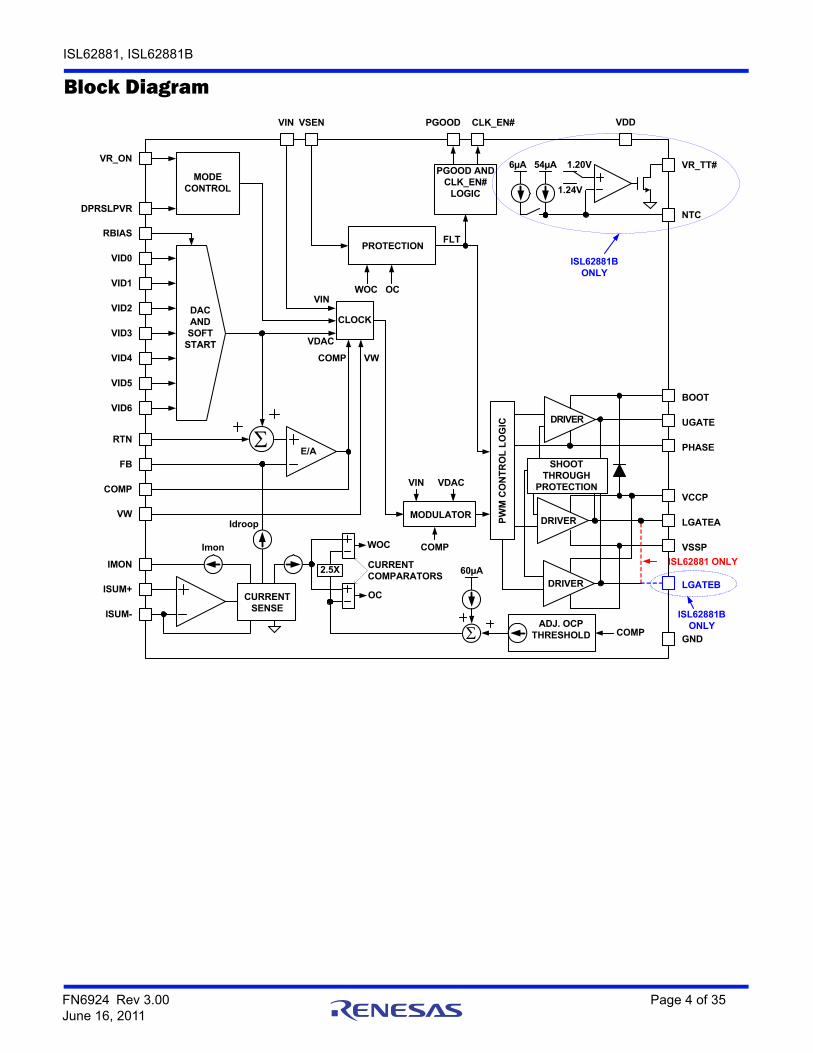
Block Diagram
VID0
VID1
VID2
VID3
VID4
VID5
VID6
VR_ON
DPRSLPVR
MODE CONTROL
DACANDSOFT
START
RTN E/A
FB
Idroop
CURRENTSENSE
ISUM+
ISUM-
Imon
IMON
COMP
PROTECTION
PGOOD CLK_EN#
ADJ. OCP THRESHOLD
VSEN
CLOCK
VW
VIN
FLT
WOC
OC
2.5X
WOC OCVIN
VDAC
MODULATOR
VIN VDAC
COMP VW
COMP
PGOOD AND CLK_EN#
LOGIC
GND
VDD
RBIAS
60µA
CURRENT COMPARATORS
COMP
DRIVER
SHOOT THROUGH
PROTECTION
DRIVERPW
M C
ON
TR
OL
LO
GIC
LGATEA
PHASE
UGATE
BOOT
VSSP
VCCP
DRIVER LGATEB
VR_TT#
NTC
1.20V
1.24V
54µA6µA
ISL62881B ONLY
ISL62881 ONLY
ISL62881B ONLY
FN6924 Rev 3.00 Page 4 of 35June 16, 2011
ISL62881, ISL62881B
Absolute Maximum Ratings Thermal InformationSupply Voltage, VDD. . . . . . . . . . . . . . . . . . . . . . . . . . . . . . . . . . . -0.3V to +7VBattery Voltage, VIN . . . . . . . . . . . . . . . . . . . . . . . . . . . . . . . . . . . . . . . . . +28VBoot Voltage (BOOT) . . . . . . . . . . . . . . . . . . . . . . . . . . . . . . . . . . -0.3V to +33VBoot to Phase Voltage (BOOT-PHASE) . . . . . . . . . . . . . . . . -0.3V to +7V(DC)
. . . . . . . . . . . . . . . . . . . . . . . . . . . . . . . . . . . . . . . . . . . -0.3V to +9V(<10ns)Phase Voltage (PHASE) . . . . . . . . . . . . . . . . -7V (<20ns Pulse Width, 10µJ)UGATE Voltage (UGATE) . . . . . . . . . . . . . . . . . . . . PHASE-0.3V (DC) to BOOT
. . . . . . . . . . . . . . . . . . . . .PHASE-5V (<20ns Pulse Width, 10µJ) to BOOTLGATE Voltage (LGATE). . . . . . . . . . . . . . . . . . . . . . -0.3V (DC) to VDD + 0.3V
. . . . . . . . . . . . . . . . . . . . . -2.5V (<20ns Pulse Width, 5µJ) to VDD + 0.3VAll Other Pins . . . . . . . . . . . . . . . . . . . . . . . . . . . . . . . . -0.3V to (VDD + 0.3V)Open Drain Outputs, PGOOD, VR_TT#, CLK_EN# . . . . . . . . . . . . . . -0.3V to +7V
Thermal Resistance (Typical, Notes 4, 5) JA (°C/W) JC (°C/W)28 Ld TQFN Package . . . . . . . . . . . . . . . . . . 40 332 Ld TQFN Package . . . . . . . . . . . . . . . . . . 32 3
Maximum Junction Temperature . . . . . . . . . . . . . . . . . . . . . . . . . . . .+150°CMaximum Storage Temperature Range . . . . . . . . . . . . . .-65°C to +150°CPb-Free Reflow Profile . . . . . . . . . . . . . . . . . . . . . . . . . . . . . . . see link below
http://www.intersil.com/pbfree/Pb-FreeReflow.asp
Recommended Operating ConditionsSupply Voltage, VDD. . . . . . . . . . . . . . . . . . . . . . . . . . . . . . . . . . . . . .+5V ±5%Battery Voltage, VIN . . . . . . . . . . . . . . . . . . . . . . . . . . . . . . . . . . +4.5V to 25VAmbient Temperature . . . . . . . . . . . . . . . . . . . . . . . . . . . . .-10°C to +100°CJunction Temperature . . . . . . . . . . . . . . . . . . . . . . . . . . . . .-10°C to +125°C
CAUTION: Do not operate at or near the maximum ratings listed for extended periods of time. Exposure to such conditions may adversely impact productreliability and result in failures not covered by warranty.
NOTES:
4. JA is measured in free air with the component mounted on a high effective thermal conductivity test board with “direct attach” features. See Tech Brief TB379
5. For JC, the “case temp” location is the center of the exposed metal pad on the package underside.
Electrical Specifications Operating Conditions: VDD = 5V, TA = -10°C to +100°C, fSW = 300kHz, unless otherwise noted. Boldface limits apply over the operating temperature range, -10°C to +100°C.
PARAMETER SYMBOL TEST CONDITIONSMIN
(Note 6) TYPMAX
(Note 6) UNITS
INPUT POWER SUPPLY
+5V Supply Current IVDD VR_ON = 1V 3.2 4.0 mA
VR_ON = 0V 1 µA
Battery Supply Current IVIN VR_ON = 0V 1 µA
VIN Input Resistance RVIN VR_ON = 1V 900 k
Power-On-Reset Threshold PORr VDD rising 4.35 4.5 V
PORf VDD falling 4.00 4.15 V
SYSTEM AND REFERENCES
System Accuracy %Error (VCC_CORE) No load; closed loop, active mode rangeVID = 0.75V to 1.50V
-0.5 +0.5 %
VID = 0.5V to 0.7375V -8 +8 mV
VID = 0.3V to 0.4875V -15 +15 mV
VBOOT 1.0945 1.100 1.1055 V
Maximum Output Voltage VCC_CORE(max) VID = [0000000] 1.500 V
Minimum Output Voltage VCC_CORE(min) VID = [1111111] 0 V
RBIAS Voltage RBIAS = 147k 1.45 1.47 1.49 V
CHANNEL FREQUENCY
Nominal Channel Frequency fSW(nom) RFSET = 7k, VCOMP = 1V 295 310 325 kHz
Adjustment Range 200 500 kHz
AMPLIFIERS
Current-Sense Amplifier Input Offset
IFB = 0A -0.15 +0.15 mV
Error Amp DC Gain Av0 90 dB
Error Amp Gain-Bandwidth Product
GBW CL = 20pF 18 MHz
FN6924 Rev 3.00 Page 5 of 35June 16, 2011
ISL62881, ISL62881B
POWER GOOD AND PROTECTION MONITORS
PGOOD Low Voltage VOL IPGOOD = 4mA 0.26 0.4 V
PGOOD Leakage Current IOH PGOOD = 3.3V -1 1 µA
PGOOD Delay tpgd CLK_ENABLE# LOW to PGOOD HIGH 6.3 7.6 8.9 ms
UGATE DRIVER
UGATE Pull-Up Resistance RUGPU 200mA Source Current 1.0 1.5
UGATE Source Current IUGSRC BOOT - UGATE = 2.5V 2.0 A
UGATE Sink Resistance RUGPD 250mA Sink Current 1.0 1.5
UGATE Sink Current IUGSNK UGATE - PHASE = 2.5V 2.0 A
LGATE DRIVER For ISL62881
LGATE Pull-Up Resistance RLGPU 250mA Source Current 1.0 1.5
LGATE Source Current ILGSRC VCCP - LGATE = 2.5V 2.0 A
LGATE Sink Resistance RLGPD 250mA Sink Current 0.5 0.9
LGATE Sink Current ILGSNK LGATE - VSSP = 2.5V 4.0 A
UGATE to LGATE Deadtime tUGFLGR UGATE falling to LGATE rising, no load 23 ns
LGATE to UGATE Deadtime tLGFUGR LGATE falling to UGATE rising, no load 28 ns
LGATE DRIVERS For ISL62881B
LGATEa and b Pull-Up Resistance RLGPU 250mA Source Current 2.0 3
LGATEa and b Source Current ILGSRC VCCP - LGATEa and b = 2.5V 1.0 A
LGATEa and b Sink Resistance RLGPD 250mA Sink Current 1 1.8
LGATEa and b Sink Current ILGSNK LGATEa and b - VSSP = 2.5V 2.0 A
UGATE to LGATEa and b Deadtime
tUGFLGR UGATE falling to LGATEa and b rising, no load 23 ns
LGATEa and b to UGATE Deadtime
tLGFUGR LGATEa and b falling to UGATE rising, no load 28 ns
BOOTSTRAP DIODE
Forward Voltage VF PVCC = 5V, IF = 2mA 0.58 V
Reverse Leakage IR VR = 25V 0.2 µA
PROTECTION
Overvoltage Threshold OVH VSEN rising above setpoint for >1ms 150 200 240 mV
Severe Overvoltage Threshold OVHS VSEN rising for >2µs 1.525 1.55 1.575 V
OC Threshold Offset ISUM- pin current 8.2 10.1 12 µA
Undervoltage Threshold UVf VSEN falling below setpoint for >1.2ms -355 -295 -235 mV
LOGIC THRESHOLDS
VR_ON Input Low VIL(1.0V) 0.3 V
VR_ON Input High VIH(1.0V) 0.7 V
VID0-VID6 and DPRSLPVR Input Low
VIL(1.0V) 0.3 V
VID0-VID6 and DPRSLPVR Input High
VIH(1.0V) 0.7 V
THERMAL MONITOR (For ISL62881B)
NTC Source Current NTC = 1.3V 53 60 67 µA
Electrical Specifications Operating Conditions: VDD = 5V, TA = -10°C to +100°C, fSW = 300kHz, unless otherwise noted. Boldface limits apply over the operating temperature range, -10°C to +100°C. (Continued)
PARAMETER SYMBOL TEST CONDITIONSMIN
(Note 6) TYPMAX
(Note 6) UNITS
FN6924 Rev 3.00 Page 6 of 35June 16, 2011
ISL62881, ISL62881B
Over-Temperature Threshold V (NTC) falling 1.18 1.2 1.22 V
VR_TT# Low Output Resistance RTT I = 20mA 6.5 9
CLK_EN# OUTPUT LEVELS
CLK_EN# Low Output Voltage VOL I = 4mA 0.26 0.4 V
CLK_EN# Leakage Current IOH CLK_EN# = 3.3V -1 1 µA
CURRENT MONITOR
IMON Output Current IIMON ISUM- pin current = 20µA 108 120 132 µA
ISUM- pin current = 10µA 51 60 69 µA
ISUM- pin current = 5µA 22 30 37.5 µA
IMON Clamp Voltage VIMONCLAMP 1.1 1.15 V
Current Sinking Capability 275 µA
INPUTS
VR_ON Leakage Current IVR_ON VR_ON = 0V -1 0 µA
VR_ON = 1V 0 1 µA
VIDx Leakage Current IVIDx VIDx = 0V -1 0 µA
VIDx = 1V 0.45 1 µA
DPRSLPVR Leakage Current IDPRSLPVR DPRSLPVR = 0V -1 0 µA
DPRSLPVR = 1V 0.45 1 µA
SLEW RATE
Slew Rate (For VID Change) SR 5 6.5 mV/µs
NOTE:6. Parameters with MIN and/or MAX limits are 100% tested at +25°C, unless otherwise specified. Temperature limits established by characterization
and are not production tested.
Electrical Specifications Operating Conditions: VDD = 5V, TA = -10°C to +100°C, fSW = 300kHz, unless otherwise noted. Boldface limits apply over the operating temperature range, -10°C to +100°C. (Continued)
PARAMETER SYMBOL TEST CONDITIONSMIN
(Note 6) TYPMAX
(Note 6) UNITS
FN6924 Rev 3.00 Page 7 of 35June 16, 2011
ISL62881, ISL62881B
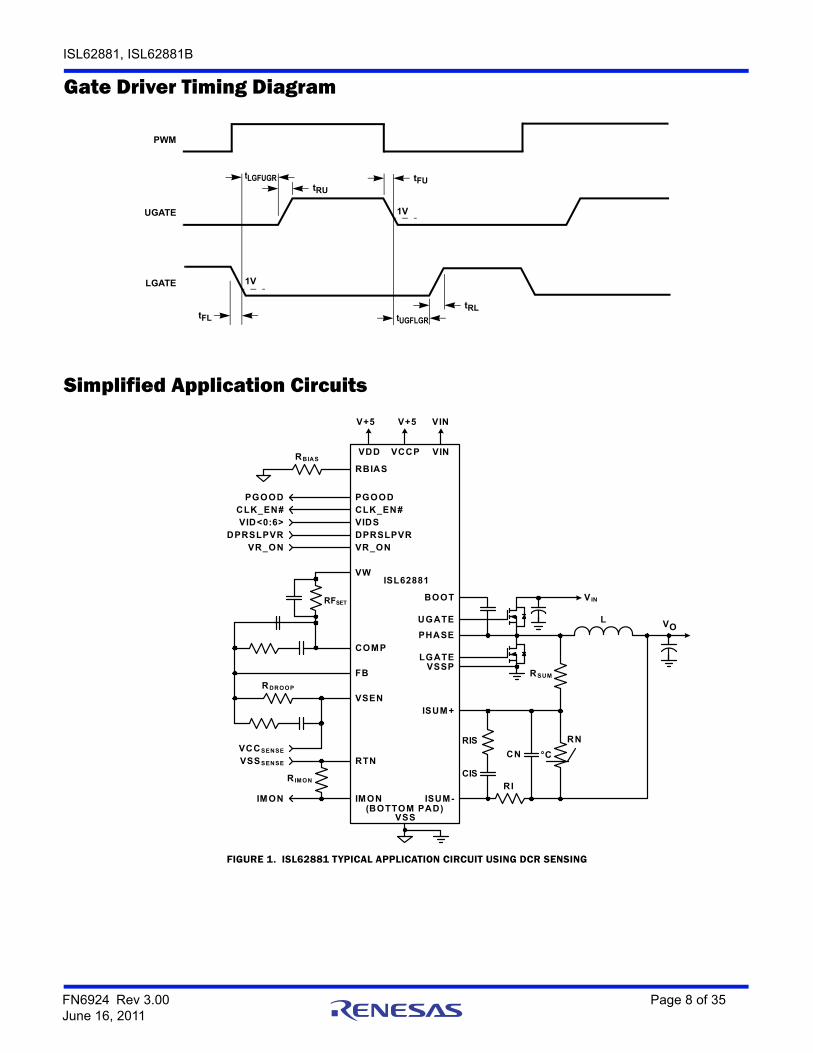
Gate Driver Timing Diagram
Simplified Application Circuits
FIGURE 1. ISL62881 TYPICAL APPLICATION CIRCUIT USING DCR SENSING
PWM
UGATE
LGATE 1V
1V
tUGFLGR
tRL
tFUtRU
tFL
tLGFUGR
(BOTTOM PAD)VSS
FB
VSEN
COMP
RDROOP
RFSET
VW
RTN
VR_ONDPRSLPVRVIDS
RBIAS
CLK_EN#
V+5
VDD
IMON
CLK_EN#VID<0:6>
DPRSLPVRVR_ON
PGOOD
RIMON
VSSSENSE
VCCSENSE
IMON
PGOOD
V+5
VCCP
ISL62881
RBIAS
L VO
RSUM
RN
CN
RI
VIN
PHASE
UGATE
BOOT
LGATE
ISUM+
ISUM-
VSSP
RIS
CIS
VIN
VIN
°C
FN6924 Rev 3.00 Page 8 of 35June 16, 2011
ISL62881, ISL62881B
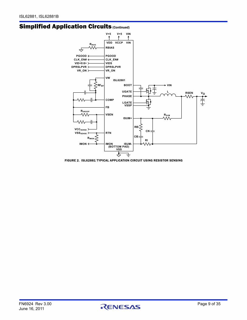
FIGURE 2. ISL62881 TYPICAL APPLICATION CIRCUIT USING RESISTOR SENSING
Simplified Application Circuits (Continued)
(BOTTOM PAD)VSS
FB
VSEN
COMP
RDROOP
RFSET
VW
RTN
VR_ONDPRSLPVRVIDS
RBIAS
CLK_EN#
V+5
VDD
IMON
CLK_EN#VID<0:6>
DPRSLPVRVR_ON
PGOOD
RIMON
VSSSENSE
VCCSENSE
IMON
PGOOD
V+5
VCCP
ISL62881
RBIAS
CN
RI
VIN
PHASE
UGATE
BOOT
LGATE
ISUM+
ISUM-
VSSP
RIS
CIS
VIN
VIN
L VO
RSUM
RSEN
FN6924 Rev 3.00 Page 9 of 35June 16, 2011
ISL62881, ISL62881B
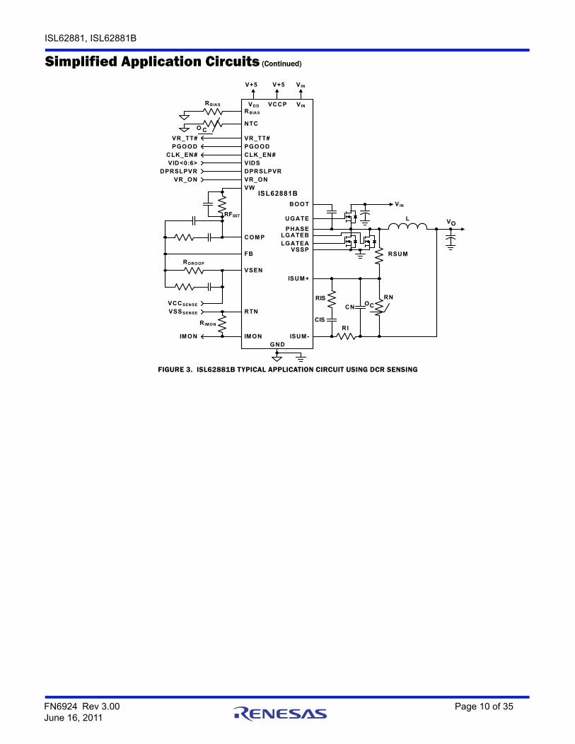
FIGURE 3. ISL62881B TYPICAL APPLICATION CIRCUIT USING DCR SENSING
Simplified Application Circuits (Continued)
GND
FB
VSEN
COMP
RDROOP
RFSET
VW
RTN
VR_ONDPRSLPVRVIDS
RBIAS
CLK_EN#
V+5
VDD
IMON
CLK_EN#VID<0:6>
DPRSLPVRVR_ON
PGOOD
RIMON
VSSSENSE
VCCSENSE
IMON
PGOOD
V+5
VCCP
ISL62881B
RBIAS
L VO
RSUM
RN
CN
RI
VIN
PHASE
UGATE
BOOT
LGATEA
ISUM+
ISUM-
VSSP
OCRIS
CIS
VIN
VIN
NTCO C
VR_TT# VR_TT#
LGATEB
FN6924 Rev 3.00 Page 10 of 35June 16, 2011
ISL62881, ISL62881B
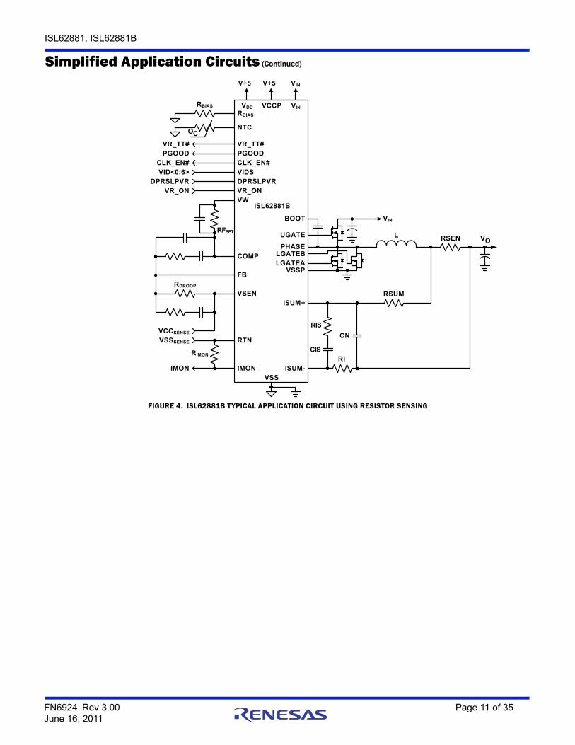
FIGURE 4. ISL62881B TYPICAL APPLICATION CIRCUIT USING RESISTOR SENSING
Simplified Application Circuits (Continued)
VSS
V+5
VDD
V+5
VCCP
ISL62881B
CN
RI
ISUM+
ISUM-
RIS
CIS
VIN
VIN
L VO
RSUM
RSEN
VIN
PHASE
UGATE
BOOT
LGATEAVSSP
LGATEB
FB
VSEN
COMP
RDROOP
RFSET
VW
RTN
VR_ONDPRSLPVRVIDS
RBIAS
CLK_EN#
IMON
CLK_EN#VID<0:6>
DPRSLPVRVR_ON
PGOOD
RIMON
VSSSENSE
VCCSENSE
IMON
PGOOD
RBIAS
NTCOC
VR_TT# VR_TT#
FN6924 Rev 3.00 Page 11 of 35June 16, 2011
ISL62881, ISL62881B
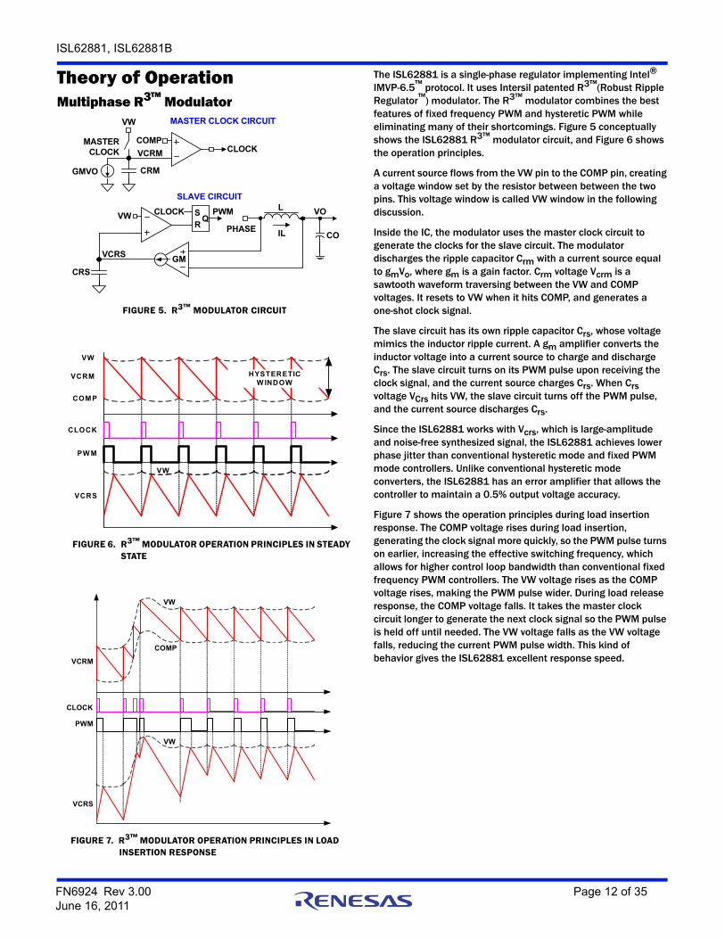
Theory of OperationMultiphase R3™ Modulator
The ISL62881 is a single-phase regulator implementing Intel® IMVP-6.5™ protocol. It uses Intersil patented R3™(Robust Ripple Regulator™) modulator. The R3™ modulator combines the best features of fixed frequency PWM and hysteretic PWM while eliminating many of their shortcomings. Figure 5 conceptually shows the ISL62881 R3™ modulator circuit, and Figure 6 shows the operation principles.
A current source flows from the VW pin to the COMP pin, creating a voltage window set by the resistor between between the two pins. This voltage window is called VW window in the following discussion.
Inside the IC, the modulator uses the master clock circuit to generate the clocks for the slave circuit. The modulator discharges the ripple capacitor Crm with a current source equal to gmVo, where gm is a gain factor. Crm voltage Vcrm is a sawtooth waveform traversing between the VW and COMP voltages. It resets to VW when it hits COMP, and generates a one-shot clock signal.
The slave circuit has its own ripple capacitor Crs, whose voltage mimics the inductor ripple current. A gm amplifier converts the inductor voltage into a current source to charge and discharge Crs. The slave circuit turns on its PWM pulse upon receiving the clock signal, and the current source charges Crs. When Crs voltage VCrs hits VW, the slave circuit turns off the PWM pulse, and the current source discharges Crs.
Since the ISL62881 works with Vcrs, which is large-amplitude and noise-free synthesized signal, the ISL62881 achieves lower phase jitter than conventional hysteretic mode and fixed PWM mode controllers. Unlike conventional hysteretic mode converters, the ISL62881 has an error amplifier that allows the controller to maintain a 0.5% output voltage accuracy.
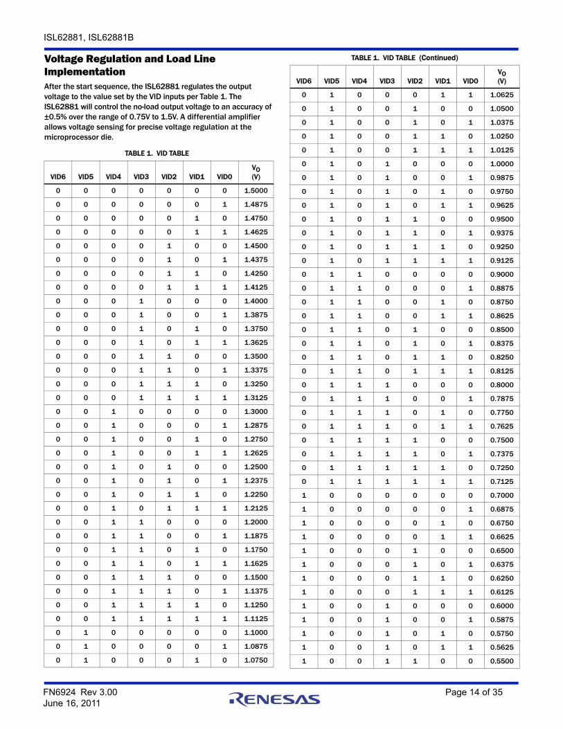
Figure 7 shows the operation principles during load insertion response. The COMP voltage rises during load insertion, generating the clock signal more quickly, so the PWM pulse turns on earlier, increasing the effective switching frequency, which allows for higher control loop bandwidth than conventional fixed frequency PWM controllers. The VW voltage rises as the COMP voltage rises, making the PWM pulse wider. During load release response, the COMP voltage falls. It takes the master clock circuit longer to generate the next clock signal so the PWM pulse is held off until needed. The VW voltage falls as the VW voltage falls, reducing the current PWM pulse width. This kind of behavior gives the ISL62881 excellent response speed.
FIGURE 5. R3™ MODULATOR CIRCUIT
CRMGMVO
MASTER CLOCK
VW
COMPCLOCK
RIL
GM
CLOCK
PHASE
CRS
VW SQ
PWM L
CO
VO
VCRM
VCRS
MASTER CLOCK CIRCUIT
SLAVE CIRCUIT
FIGURE 6. R3™ MODULATOR OPERATION PRINCIPLES IN STEADY STATE
COMP
VCRM
PW M
VW
CLOCK
HYSTERETIC W INDOW
VCRS
VW
FIGURE 7. R3™ MODULATOR OPERATION PRINCIPLES IN LOAD INSERTION RESPONSE
COMP
VCRM
PWM
VCRS
VW
CLOCK
VW
FN6924 Rev 3.00 Page 12 of 35June 16, 2011
ISL62881, ISL62881B
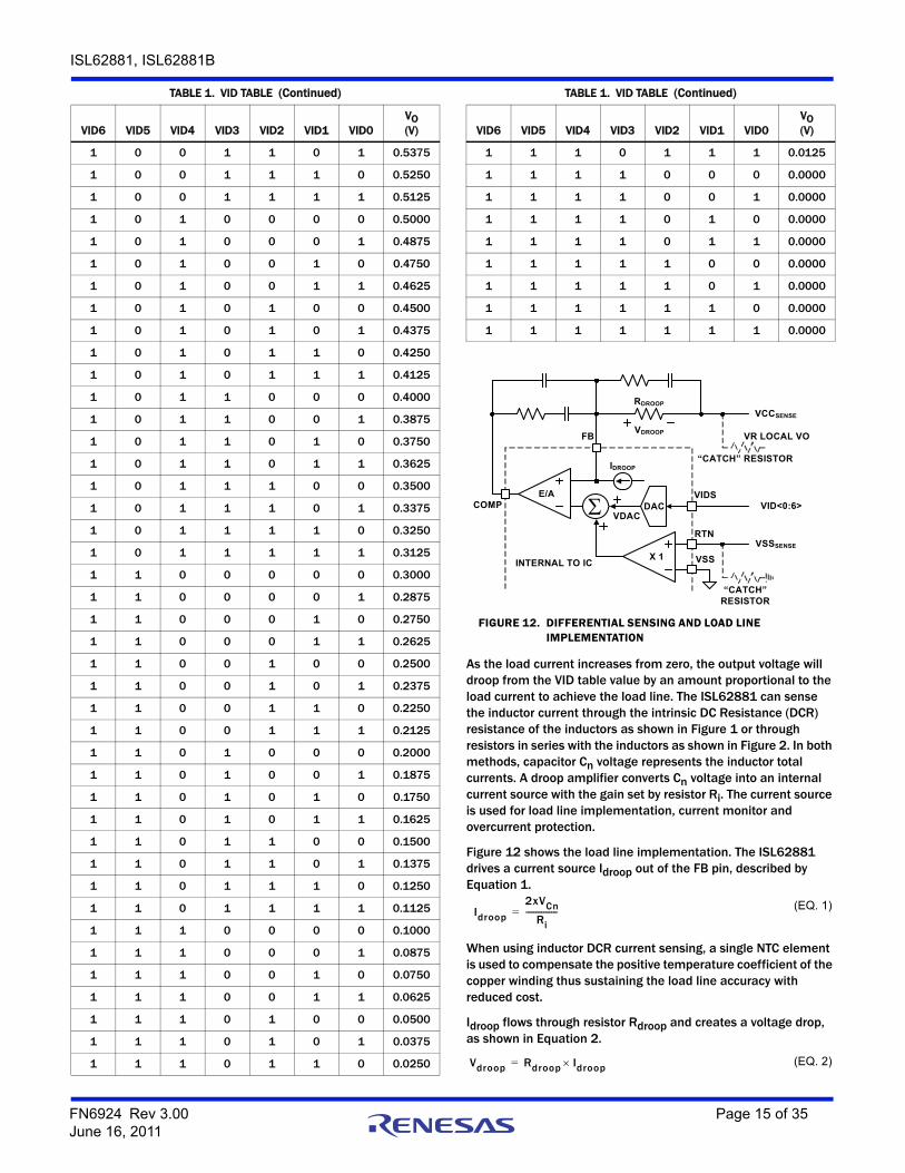
Diode Emulation and Period Stretching
ISL62881 can operate in diode emulation (DE) mode to improve light load efficiency. In DE mode, the low-side MOSFET conducts when the current is flowing from source to drain and doesn’t not allow reverse current, emulating a diode. As shown in Figure 8, when LGATE is on, the low-side MOSFET carries current, creating negative voltage on the phase node due to the voltage drop across the ON-resistance. The ISL62881 monitors the current through monitoring the phase node voltage. It turns off LGATE when the phase node voltage reaches zero to prevent the inductor current from reversing the direction and creating unnecessary power loss.
If the load current is light enough, as Figure 9 shows, the inductor current will reach and stay at zero before the next phase node pulse, and the regulator is in discontinuous conduction mode (DCM). If the load current is heavy enough, the inductor current will never reach 0A, and the regulator is in CCM although the controller is in DE mode.
Figure 9 shows the operation principle in diode emulation mode at light load. The load gets incrementally lighter in the three cases from top to bottom. The PWM on-time is determined by the VW
window size, therefore is the same, making the inductor current triangle the same in the three cases. The ISL62881 clamps the ripple capacitor voltage Vcrs in DE mode to make it mimic the inductor current. It takes the COMP voltage longer to hit Vcrs, naturally stretching the switching period. The inductor current triangles move further apart from each other such that the inductor current average value is equal to the load current. The reduced switching frequency helps increase light load efficiency.
Start-up TimingWith the controller's VDD voltage above the POR threshold, the start-up sequence begins when VR_ON exceeds the 3.3V logic high threshold.
Figure 10 shows the typical start-up timing when the ISL62881 is configured for CPU VR application. The ISL62881 uses digital soft-start to ramp up DAC to the boot voltage of 1.1V at about 2.5mV/µs. Once the output voltage is within 10% of the boot voltage for 13 PWM cycles (43µs for frequency = 300kHz), CLK_EN# is pulled low and DAC slews at 5mV/µs to the voltage set by the VID pins. PGOOD is asserted high in approximately 7ms. Similar results occur if VR_ON is tied to VDD, with the soft-start sequence starting 120µs after VDD crosses the POR threshold.
Figure 11 shows the typical start-up timing when the ISL62881 is configured for GPU VR application. The ISL62881 uses digital soft-start to ramp-up DAC to the voltage set by the VID pins at 5mV/µs. Once the output voltage is within 10% of the target voltage for 13 PWM cycles (43µs for frequency = 300kHz), CLK_EN# is pulled low. PGOOD is asserted high in approximately 7ms. Similar results occur if VR_ON is tied to VDD, with the soft-start sequence starting 120µs after VDD crosses the POR threshold.
FIGURE 8. DIODE EMULATION
U G A T E
P H A S E
IL
L G A T E
FIGURE 9. PERIOD STRETCHING
IL
IL
VCRS
IL
VCRS
VCRS
VWCCM/DCM BOUNDARY
LIGHT DCM
DEEP DCM
VW
VW
FIGURE 10. SOFT-START WAVEFORMS FOR CPU VR APPLICATION
VDD
VR_ON
DAC
800µs
2.5mV/µsVBOOT
5mV/µs
VID COMMAND VOLTAGE
90%
13 SWITCHING CYCLES
CLK_EN#
PGOOD~7ms
FIGURE 11. SOFT-START WAVEFORMS FOR GPU VR APPLICATION
VDD
VR_ON
DAC
120µs
5mV/µs VID COMMAND VOLTAGE90%
13 SWITCHING CYCLES
CLK_EN#
PGOOD~7ms
FN6924 Rev 3.00 Page 13 of 35June 16, 2011
ISL62881, ISL62881B
Voltage Regulation and Load Line ImplementationAfter the start sequence, the ISL62881 regulates the output voltage to the value set by the VID inputs per Table 1. The ISL62881 will control the no-load output voltage to an accuracy of ±0.5% over the range of 0.75V to 1.5V. A differential amplifier allows voltage sensing for precise voltage regulation at the microprocessor die.
TABLE 1. VID TABLE
VID6 VID5 VID4 VID3 VID2 VID1 VID0VO (V)
0 0 0 0 0 0 0 1.5000
0 0 0 0 0 0 1 1.4875
0 0 0 0 0 1 0 1.4750
0 0 0 0 0 1 1 1.4625
0 0 0 0 1 0 0 1.4500
0 0 0 0 1 0 1 1.4375
0 0 0 0 1 1 0 1.4250
0 0 0 0 1 1 1 1.4125
0 0 0 1 0 0 0 1.4000
0 0 0 1 0 0 1 1.3875
0 0 0 1 0 1 0 1.3750
0 0 0 1 0 1 1 1.3625
0 0 0 1 1 0 0 1.3500
0 0 0 1 1 0 1 1.3375
0 0 0 1 1 1 0 1.3250
0 0 0 1 1 1 1 1.3125
0 0 1 0 0 0 0 1.3000
0 0 1 0 0 0 1 1.2875
0 0 1 0 0 1 0 1.2750
0 0 1 0 0 1 1 1.2625
0 0 1 0 1 0 0 1.2500
0 0 1 0 1 0 1 1.2375
0 0 1 0 1 1 0 1.2250
0 0 1 0 1 1 1 1.2125
0 0 1 1 0 0 0 1.2000
0 0 1 1 0 0 1 1.1875
0 0 1 1 0 1 0 1.1750
0 0 1 1 0 1 1 1.1625
0 0 1 1 1 0 0 1.1500
0 0 1 1 1 0 1 1.1375
0 0 1 1 1 1 0 1.1250
0 0 1 1 1 1 1 1.1125
0 1 0 0 0 0 0 1.1000
0 1 0 0 0 0 1 1.0875
0 1 0 0 0 1 0 1.0750
0 1 0 0 0 1 1 1.0625
0 1 0 0 1 0 0 1.0500
0 1 0 0 1 0 1 1.0375
0 1 0 0 1 1 0 1.0250
0 1 0 0 1 1 1 1.0125
0 1 0 1 0 0 0 1.0000
0 1 0 1 0 0 1 0.9875
0 1 0 1 0 1 0 0.9750
0 1 0 1 0 1 1 0.9625
0 1 0 1 1 0 0 0.9500
0 1 0 1 1 0 1 0.9375
0 1 0 1 1 1 0 0.9250
0 1 0 1 1 1 1 0.9125
0 1 1 0 0 0 0 0.9000
0 1 1 0 0 0 1 0.8875
0 1 1 0 0 1 0 0.8750
0 1 1 0 0 1 1 0.8625
0 1 1 0 1 0 0 0.8500
0 1 1 0 1 0 1 0.8375
0 1 1 0 1 1 0 0.8250
0 1 1 0 1 1 1 0.8125
0 1 1 1 0 0 0 0.8000
0 1 1 1 0 0 1 0.7875
0 1 1 1 0 1 0 0.7750
0 1 1 1 0 1 1 0.7625
0 1 1 1 1 0 0 0.7500
0 1 1 1 1 0 1 0.7375
0 1 1 1 1 1 0 0.7250
0 1 1 1 1 1 1 0.7125
1 0 0 0 0 0 0 0.7000
1 0 0 0 0 0 1 0.6875
1 0 0 0 0 1 0 0.6750
1 0 0 0 0 1 1 0.6625
1 0 0 0 1 0 0 0.6500
1 0 0 0 1 0 1 0.6375
1 0 0 0 1 1 0 0.6250
1 0 0 0 1 1 1 0.6125
1 0 0 1 0 0 0 0.6000
1 0 0 1 0 0 1 0.5875
1 0 0 1 0 1 0 0.5750
1 0 0 1 0 1 1 0.5625
1 0 0 1 1 0 0 0.5500
TABLE 1. VID TABLE (Continued)
VID6 VID5 VID4 VID3 VID2 VID1 VID0VO (V)
FN6924 Rev 3.00 Page 14 of 35June 16, 2011
ISL62881, ISL62881B
As the load current increases from zero, the output voltage will droop from the VID table value by an amount proportional to the load current to achieve the load line. The ISL62881 can sense the inductor current through the intrinsic DC Resistance (DCR) resistance of the inductors as shown in Figure 1 or through resistors in series with the inductors as shown in Figure 2. In both methods, capacitor Cn voltage represents the inductor total currents. A droop amplifier converts Cn voltage into an internal current source with the gain set by resistor Ri. The current source is used for load line implementation, current monitor and overcurrent protection.
Figure 12 shows the load line implementation. The ISL62881 drives a current source Idroop out of the FB pin, described by Equation 1.
When using inductor DCR current sensing, a single NTC element is used to compensate the positive temperature coefficient of the copper winding thus sustaining the load line accuracy with reduced cost.
Idroop flows through resistor Rdroop and creates a voltage drop, as shown in Equation 2.
1 0 0 1 1 0 1 0.5375
1 0 0 1 1 1 0 0.5250
1 0 0 1 1 1 1 0.5125
1 0 1 0 0 0 0 0.5000
1 0 1 0 0 0 1 0.4875
1 0 1 0 0 1 0 0.4750
1 0 1 0 0 1 1 0.4625
1 0 1 0 1 0 0 0.4500
1 0 1 0 1 0 1 0.4375
1 0 1 0 1 1 0 0.4250
1 0 1 0 1 1 1 0.4125
1 0 1 1 0 0 0 0.4000
1 0 1 1 0 0 1 0.3875
1 0 1 1 0 1 0 0.3750
1 0 1 1 0 1 1 0.3625
1 0 1 1 1 0 0 0.3500
1 0 1 1 1 0 1 0.3375
1 0 1 1 1 1 0 0.3250
1 0 1 1 1 1 1 0.3125
1 1 0 0 0 0 0 0.3000
1 1 0 0 0 0 1 0.2875
1 1 0 0 0 1 0 0.2750
1 1 0 0 0 1 1 0.2625
1 1 0 0 1 0 0 0.2500
1 1 0 0 1 0 1 0.2375
1 1 0 0 1 1 0 0.2250
1 1 0 0 1 1 1 0.2125
1 1 0 1 0 0 0 0.2000
1 1 0 1 0 0 1 0.1875
1 1 0 1 0 1 0 0.1750
1 1 0 1 0 1 1 0.1625
1 1 0 1 1 0 0 0.1500
1 1 0 1 1 0 1 0.1375
1 1 0 1 1 1 0 0.1250
1 1 0 1 1 1 1 0.1125
1 1 1 0 0 0 0 0.1000
1 1 1 0 0 0 1 0.0875
1 1 1 0 0 1 0 0.0750
1 1 1 0 0 1 1 0.0625
1 1 1 0 1 0 0 0.0500
1 1 1 0 1 0 1 0.0375
1 1 1 0 1 1 0 0.0250
TABLE 1. VID TABLE (Continued)
VID6 VID5 VID4 VID3 VID2 VID1 VID0VO (V)
1 1 1 0 1 1 1 0.0125
1 1 1 1 0 0 0 0.0000
1 1 1 1 0 0 1 0.0000
1 1 1 1 0 1 0 0.0000
1 1 1 1 0 1 1 0.0000
1 1 1 1 1 0 0 0.0000
1 1 1 1 1 0 1 0.0000
1 1 1 1 1 1 0 0.0000
1 1 1 1 1 1 1 0.0000
TABLE 1. VID TABLE (Continued)
VID6 VID5 VID4 VID3 VID2 VID1 VID0VO (V)
FIGURE 12. DIFFERENTIAL SENSING AND LOAD LINE IMPLEMENTATION
X 1
E/A
DAC VID<0:6>
RDROOP
IDROOP
VDAC
VDROOPFB
COMP
VCCSENSE
VSSSENSE
VIDS
RTN
VSSINTERNAL TO IC
“CATCH” RESISTOR
“CATCH” RESISTOR
VR LOCAL VO
Idroop
2xVCnRi
----------------= (EQ. 1)
Vdroop Rdroop Idroop= (EQ. 2)
FN6924 Rev 3.00 Page 15 of 35June 16, 2011
ISL62881, ISL62881B
Vdroop is the droop voltage required to implement load line. Changing Rdroop or scaling Idroop can both change the load line slope. Since Idroop also sets the overcurrent protection level, it is recommended to first scale Idroop based on OCP requirement, then select an appropriate Rdroop value to obtain the desired load line slope.
Differential SensingFigure 12 also shows the differential voltage sensing scheme. VCCSENSE and VSSSENSE are the remote voltage sensing signals from the processor die. A unity gain differential amplifier senses the VSSSENSE voltage and adds it to the DAC output. The error amplifier regulates the inverting and the non-inverting input voltages to be equal, therefore:
Rewriting Equation 3 and substituting Equation 2 gives:
Equation 4 is the exact equation required for load line implementation.
The VCCSENSE and VSSSENSE signals come from the processor die. The feedback will be open circuit in the absence of the processor. As shown in Figure 12, it is recommended to add a “catch” resistor to feed the VR local output voltage back to the compensator, and add another “catch” resistor to connect the VR local output ground to the RTN pin. These resistors, typically 10~100, will provide voltage feedback if the system is powered up without a processor installed.
CCM Switching FrequencyThe RFSET resistor between the COMP and the VW pins sets the VW windows size, which therefore sets the switching frequency. When the ISL62881 is in continuous conduction mode (CCM), the switching frequency is not absolutely constant due to the nature of the R3™ modulator. As explained in “Multiphase R3™ Modulator” on page 12, the effective switching frequency will increase during load insertion and will decrease during load release to achieve fast response. On the other hand, the switching frequency is relatively constant at steady state. Variation is expected when the power stage condition, such as input voltage, output voltage, load, etc. changes. The variation is usually less than 15% and doesn’t have any significant effect on output voltage ripple magnitude. Equation 5 gives an estimate of the frequency-setting resistor Rfset value. 8k RFSET gives approximately 300kHz switching frequency. Lower resistance gives higher switching frequency.
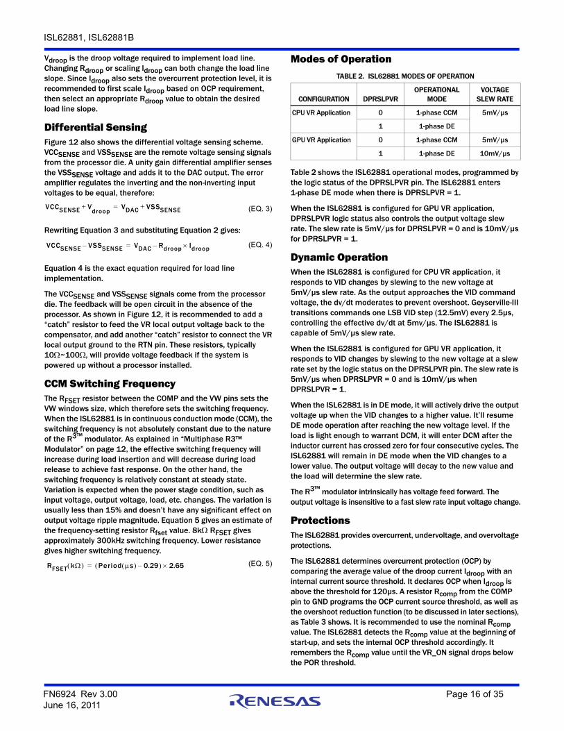
Modes of Operation
Table 2 shows the ISL62881 operational modes, programmed by the logic status of the DPRSLPVR pin. The ISL62881 enters 1-phase DE mode when there is DPRSLPVR = 1.
When the ISL62881 is configured for GPU VR application, DPRSLPVR logic status also controls the output voltage slew rate. The slew rate is 5mV/µs for DPRSLPVR = 0 and is 10mV/µs for DPRSLPVR = 1.
Dynamic OperationWhen the ISL62881 is configured for CPU VR application, it responds to VID changes by slewing to the new voltage at 5mV/µs slew rate. As the output approaches the VID command voltage, the dv/dt moderates to prevent overshoot. Geyserville-III transitions commands one LSB VID step (12.5mV) every 2.5µs, controlling the effective dv/dt at 5mv/µs. The ISL62881 is capable of 5mV/µs slew rate.
When the ISL62881 is configured for GPU VR application, it responds to VID changes by slewing to the new voltage at a slew rate set by the logic status on the DPRSLPVR pin. The slew rate is 5mV/µs when DPRSLPVR = 0 and is 10mV/µs when DPRSLPVR = 1.
When the ISL62881 is in DE mode, it will actively drive the output voltage up when the VID changes to a higher value. It’ll resume DE mode operation after reaching the new voltage level. If the load is light enough to warrant DCM, it will enter DCM after the inductor current has crossed zero for four consecutive cycles. The ISL62881 will remain in DE mode when the VID changes to a lower value. The output voltage will decay to the new value and the load will determine the slew rate.
The R3™ modulator intrinsically has voltage feed forward. The output voltage is insensitive to a fast slew rate input voltage change.
ProtectionsThe ISL62881 provides overcurrent, undervoltage, and overvoltage protections.
The ISL62881 determines overcurrent protection (OCP) by comparing the average value of the droop current Idroop with an internal current source threshold. It declares OCP when Idroop is above the threshold for 120µs. A resistor Rcomp from the COMP pin to GND programs the OCP current source threshold, as well as the overshoot reduction function (to be discussed in later sections), as Table 3 shows. It is recommended to use the nominal Rcomp value. The ISL62881 detects the Rcomp value at the beginning of start-up, and sets the internal OCP threshold accordingly. It remembers the Rcomp value until the VR_ON signal drops below the POR threshold.
VCCSENSE V+droop
VDAC VSSSENSE+= (EQ. 3)
VCCSENSE VSSSENSE– VDAC Rdroop Idroop–= (EQ. 4)
RFSET k Period s 0.29– 2.65= (EQ. 5)
TABLE 2. ISL62881 MODES OF OPERATION
CONFIGURATION DPRSLPVROPERATIONAL
MODEVOLTAGE
SLEW RATE
CPU VR Application 0 1-phase CCM 5mV/µs
1 1-phase DE
GPU VR Application 0 1-phase CCM 5mV/µs
1 1-phase DE 10mV/µs
FN6924 Rev 3.00 Page 16 of 35June 16, 2011
ISL62881, ISL62881B
The default OCP threshold is the value when Rcomp is not populated. It is recommended to scale the droop current Idroop such that the default OCP threshold gives approximately the desired OCP level, then use Rcomp to fine tune the OCP level if necessary.
For overcurrent condition above 2.5x the OCP level, the PWM output will immediately shut off and PGOOD will go low to maximize protection. This protection is also referred to as way-overcurrent protection or fast-overcurrent protection, for short-circuit protections.
The ISL62881 will declare undervoltage (UV) fault and latch-off if the output voltage is less than the VID set value by 300mV or more for 1ms. It’ll turn off the PWM output and de-assert PGOOD.
The ISL62881 has two levels of overvoltage protections. The first level of overvoltage protection is referred to as PGOOD overvoltage protection. If the output voltage exceeds the VID set value by +200mV for 1ms, the ISL62881 will declare a fault and de-assert PGOOD.
The ISL62881 takes the same actions for all of the above fault protections: de-assertion of PGOOD and turn-off of the high-side and low-side power MOSFETs. Any residual inductor current will decay through the MOSFET body diodes. These fault conditions can be reset by bringing VR_ON low or by bringing VDD below the POR threshold. When VR_ON and VDD return to their high operating levels, a soft-start will occur.
The second level of overvoltage protection is different. If the output voltage exceeds 1.55V, the ISL62881 will immediately declare an OV fault, de-assert PGOOD, and turn on the low-side power MOSFETs. The low-side power MOSFETs remain on until the output voltage is pulled down below 0.85V when all power MOSFETs are turned off. If the output voltage rises above 1.55V again, the protection process is repeated. This behavior provides the maximum amount of protection against shorted high-side power MOSFETs while preventing output ringing below ground. Resetting VR_ON cannot clear the 1.55V OVP. Only resetting VDD will clear it. The 1.55V OVP is active all the time when the controller is enabled, even if one of the other faults have been declared. This ensures that the processor is protected against high-side power MOSFET leakage while the MOSFETs are commanded off.
Table 4 summarizes the fault protections.
Current MonitorThe ISL62881 provides the current monitor function. The IMON pin outputs a high-speed analog current source that is 3 times of the droop current flowing out of the FB pin. Thus as shown by Equation 6.
As Figures 1 and 2 show, a resistor Rimon is connected to the IMON pin to convert the IMON pin current to voltage. A capacitor can be paralleled with Rimon to filter the voltage information. The IMVP-6.5™ specification requires that the IMON voltage information be referenced to VSSSENSE.
The IMON pin voltage range is 0V to 1.1V. A clamp circuit prevents the IMON pin voltage from going above 1.1V.
Adaptive Body Diode Conduction Time ReductionIn DCM, the controller turns off the low-side MOSFET when the inductor current approaches zero. During on-time of the low-side MOSFET, phase voltage is negative and the amount is the MOSFET RDS(ON) voltage drop, which is proportional to the inductor current. A phase comparator inside the controller monitors the phase voltage during on-time of the low-side MOSFET and compares it with a threshold to determine the zero-crossing point of the inductor current. If the inductor current has not reached zero when the low-side MOSFET turns off, it’ll flow through the low-side MOSFET body diode, causing the phase node to have a larger voltage drop until it decays to zero. If the inductor current has crossed zero and reversed the direction when the low-side MOSFET turns off, it’ll flow through the high-side MOSFET body diode, causing the phase node to have a spike until it decays to zero. The controller continues monitoring the phase voltage after turning off the low-side MOSFET and adjusts the phase comparator threshold voltage accordingly in iterative steps such that the low-side MOSFET body diode conducts for approximately 40ns to minimize the body diode-related loss.
TABLE 3. ISL62881 OCP THRESHOLD AND OVERSHOOT REDUCTION FUNCTION
Rcomp OCPTHRESHOLD
(µA)
OVERSHOOTREDUCTIONFUNCTION
MIN(k)
NOMINAL (k)
MAX(k)
none none 20 Disabled
305 400 410 22.67
205 235 240 20.67
155 165 170 18
104 120 130 20 Enabled
78 85 90 22.67
62 66 68 20.67
45 50 55 18
TABLE 4. FAULT PROTECTION SUMMARY
FAULT TYPE
FAULT DURATION BEFORE
PROTECTIONPROTECTION
ACTIONFAULT RESET
Overcurrent 120µs PWM tri-state, PGOOD latched low
VR_ON toggle or VDD toggle
Way-Overcurrent (2.5xOC)
<2µs
Overvoltage +200mV 1ms
Undervoltage -300mV
Overvoltage 1.55V Immediately Low-side MOSFET on until Vcore <0.85V, then PWM tri-state, PGOOD latched low.
VDD toggle
IIMON 3 Idroop= (EQ. 6)
FN6924 Rev 3.00 Page 17 of 35June 16, 2011
ISL62881, ISL62881B
Overshoot Reduction FunctionThe ISL62881 has an optional overshoot reduction function, enabled or disabled by the resistor from the COMP pin to GND, as shown in Table 3.
When a load release occurs, the energy stored in the inductors will dump to the output capacitor, causing output voltage overshoot. The inductor current freewheels through the low-side MOSFET during this period of time. The overshoot reduction function turns off the low-side MOSFET during the output voltage overshoot, forcing the inductor current to freewheel through the low-side MOSFET body diode. Since the body diode voltage drop is much higher than MOSFET RDS(ON) voltage drop, more energy is dissipated on the low-side MOSFET therefore the output voltage overshoot is lower.
If the overshoot reduction function is enabled, the ISL62881 monitors the COMP pin voltage to determine the output voltage overshoot condition. The COMP voltage will fall and hit the clamp voltage when the output voltage overshoots. The ISL62881 will turn off LGATE when COMP is being clamped. The low-side MOSFET in the power stage will be turned off. When the output voltage has reached its peak and starts to come down, the COMP voltage starts to rise and is no longer clamped. The ISL62881 will resume normal PWM operation.
While the overshoot reduction function reduces the output voltage overshoot, energy is dissipated on the low-side MOSFET, causing additional power loss. The more frequent the transient event, the more power loss is dissipated on the low-side MOSFET. The MOSFET may face severe thermal stress when transient events happen at a high repetitive rate. User discretion is advised when this function is enabled.
Key Component SelectionRBIASThe ISL62881 uses a resistor (1% or better tolerance is recommended) from the RBIAS pin to GND to establish highly accurate reference current sources inside the IC. Using RBIAS = 147k sets the controller for CPU core application and using RBIAS = 47k sets the controller for GPU core application. Do not connect any other components to this pin. Do not connect any capacitor to the RBIAS pin as it will create instability.
Care should be taken in layout that the resistor is placed very close to the RBIAS pin and that a good quality signal ground is connected to the opposite side of the RBIAS resistor.
Ris and CisAs Figures 1 and 2 show, the ISL62881 needs the Ris - Cis network across the ISUM+ and the ISUM- pins to stabilize the droop amplifier. The preferred values are Ris = 82.5 and Cis = 0.01µF. Slight deviations from the recommended values are acceptable. Large deviations may result in instability.
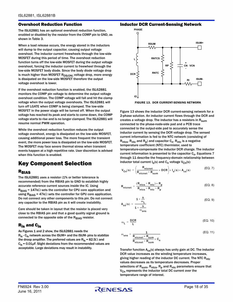
Inductor DCR Current-Sensing Network
Figure 13 shows the inductor DCR current-sensing network for a 2-phase solution. An inductor current flows through the DCR and creates a voltage drop. The inductor has a resistors in Rsum connected to the phase-node-side pad and a PCB trace connected to the output-side pad to accurately sense the inductor current by sensing the DCR voltage drop. The sensed current information is fed to the NTC network (consisting of Rntcs, Rntc and Rp) and capacitor Cn. Rntc is a negative temperature coefficient (NTC) thermistor, used to temperature-compensate the inductor DCR change. The inductor current information is presented to the capacitor Cn. Equations 7 through 11 describe the frequency-domain relationship between inductor total current Io(s) and Cn voltage VCn(s):
Transfer function Acs(s) always has unity gain at DC. The inductor DCR value increases as the winding temperature increases, giving higher reading of the inductor DC current. The NTC Rntc values decreases as its temperature decreases. Proper selections of Rsum, Rntcs, Rp and Rntc parameters ensure that VCn represents the inductor total DC current over the temperature range of interest.
CN
RSUM
RNTCS
RNTC
RP
DCR
L
PHASE
IO
RI
ISUM+
ISUM-
VCN+
-
FIGURE 13. DCR CURRENT-SENSING NETWORK
VCn s Rntcnet
Rntcnet Rsum+----------------------------------------- DCR
Io s Acs s =(EQ. 7)
Rntcnet
Rntcs Rntc+ Rp
Rntcs Rntc Rp+ +---------------------------------------------------= (EQ. 8)
Acs s
1sL------+
1s
sns------------+
----------------------=(EQ. 9)
LDCR
L------------= (EQ. 10)
sns1
Rntcnet Rsum
Rntcnet Rsum+----------------------------------------- Cn
------------------------------------------------------=(EQ. 11)
FN6924 Rev 3.00 Page 18 of 35June 16, 2011
ISL62881, ISL62881B
There are many sets of parameters that can properly temperature-compensate the DCR change. Since the NTC network and the Rsum resistors form a voltage divider, Vcn is always a fraction of the inductor DCR voltage. It is recommended to have a higher ratio of Vcn to the inductor DCR voltage, so the droop circuit has higher signal level to work with.
A typical set of parameters that provide good temperature compensation are: Rsum = 3.65k, Rp = 11k, Rntcs = 2.61k and Rntc = 10k(ERT-J1VR103J). The NTC network parameters may need to be fine tuned on actual boards. One can apply full load DC current and record the output voltage reading immediately; then record the output voltage reading again when the board has reached the thermal steady state. A good NTC network can limit the output voltage drift to within 2mV. It is recommended to follow the Intersil evaluation board layout and current-sensing network parameters to minimize engineering time.
VCn(s) also needs to represent real-time Io(s) for the controller to achieve good transient response. Transfer function Acs(s) has a pole sns and a zero L. One needs to match L and sns so Acs(s) is unity gain at all frequencies. By forcing L equal to sns and solving for the solution, Equation 12 gives Cn value.
For example, given Rsum = 3.65k, Rp = 11k, Rntcs = 2.61k, Rntc = 10k, DCR = 1.1m and L = 0.45µH, Equation 12 gives Cn = 0.18µF.
Assuming the compensator design is correct, Figure 14 shows the expected load transient response waveforms if Cn is correctly selected. When the load current Icore has a square change, the output voltage Vcore also has a square response.
If Cn value is too large or too small, VCn(s) will not accurately represent real-time Io(s) and will worsen the transient response. Figure 15 shows the load transient response when Cn is too small. Vcore will sag excessively upon load insertion and may create a system failure. Figure 16 shows the transient response when Cn is too large. Vcore is sluggish in drooping to its final value. There will be excessive overshoot if load insertion occurs during this time, which may potentially hurt the CPU reliability.
Figure 17 shows the output voltage ring back problem during load transient response. The load current io has a fast step change, but the inductor current iL cannot accurately follow. Instead, iL responds in first order system fashion due to the nature of current loop. The ESR and ESL effect of the output capacitors makes the output voltage Vo dip quickly upon load current change. However, the controller regulates Vo according to the droop current idroop, which is a real-time representation of iL; therefore it pulls Vo back to the level dictated by iL, causing the ring back problem. This phenomenon is not observed when the output capacitors have very low ESR and ESL, such as all ceramic capacitors.
CnL
Rntcnet Rsum
Rntcnet Rsum+----------------------------------------- DCR
------------------------------------------------------------= (EQ. 12)
FIGURE 14. DESIRED LOAD TRANSIENT RESPONSE WAVEFORMS
oi
Vo
FIGURE 15. LOAD TRANSIENT RESPONSE WHEN Cn IS TOO SMALL
oi
Vo
FIGURE 16. LOAD TRANSIENT RESPONSE WHEN Cn IS TOO LARGE
oi
Vo
FIGURE 17. OUTPUT VOLTAGE RING BACK PROBLEM
iO
VO
iL
RING BACK
FIGURE 18. OPTIONAL CIRCUITS FOR RING BACK REDUCTION
Cn.2
Rntcs
Rntc
Rp
Ri
ISUM+
ISUM-
Rip Cip
OPTIONAL
Vcn
Cn.1
Rn
OPTIONAL
+
-
FN6924 Rev 3.00 Page 19 of 35June 16, 2011
ISL62881, ISL62881B
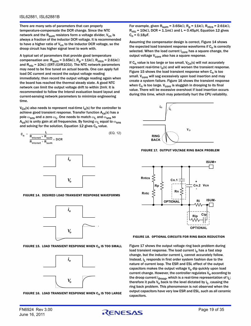
Figure 18 shows two optional circuits for reduction of the ring back. Rip and Cip form an R-C branch in parallel with Ri, providing a lower impedance path than Ri at the beginning of io change. Rip and Cip do not have any effect at steady state. Through proper selection of Rip and Cip values, idroop can resemble io rather than iL, and Vo will not ring back. The recommended value for Rip is 100W. Cip should be determined through tuning the load transient response waveforms on an actual board. The recommended range for Cip is 100pF~2000pF.
Cn is the capacitor used to match the inductor time constant. It usually takes the parallel of two (or more) capacitors to get the desired value. Figure 18 shows that two capacitors Cn.1 and Cn.2 are in parallel. Resistor Rn is an optional component to reduce the Vo ring back. At steady state, Cn.1 + Cn.2 provides the desired Cn capacitance. At the beginning of io change, the effective capacitance is less because Rn increases the impedance of the Cn.1 branch. As Figure 15 explains, Vo tends to dip when Cn is too small, and this effect will reduce the Vo ring back. This effect is more pronounced when Cn.1 is much larger than Cn.2. It is also more pronounced when Rn is bigger. However, the presence of Rn increases the ripple of the Vn signal if Cn.2 is too small. It is recommended to keep Cn.2 greater than 2200pF. Rn value usually is a few ohms. Cn.1, Cn.2 and Rn values should be determined through tuning the load transient response waveforms on an actual board.
Rip and Cip form an R-C branch in parallel with Ri, providing a lower impedance path than Ri at the beginning of io change. Rip and Cip do not have any effect at steady state. Through proper selection of Rip and Cip values, idroop can resemble io rather than iL, and Vo will not ring back. The recommended value for Rip is 100. Cip should be determined through tuning the load transient response waveforms on an actual board. The recommended range for Cip is 100pF~2000pF. However, it should be noted that the Rip -Cip branch may distort the idroop waveform. Instead of being triangular as the real inductor current, idroop may have sharp spikes, which may adversely affect idroop average value detection and therefore may affect OCP accuracy. User discretion is advised.
Resistor Current-Sensing Network
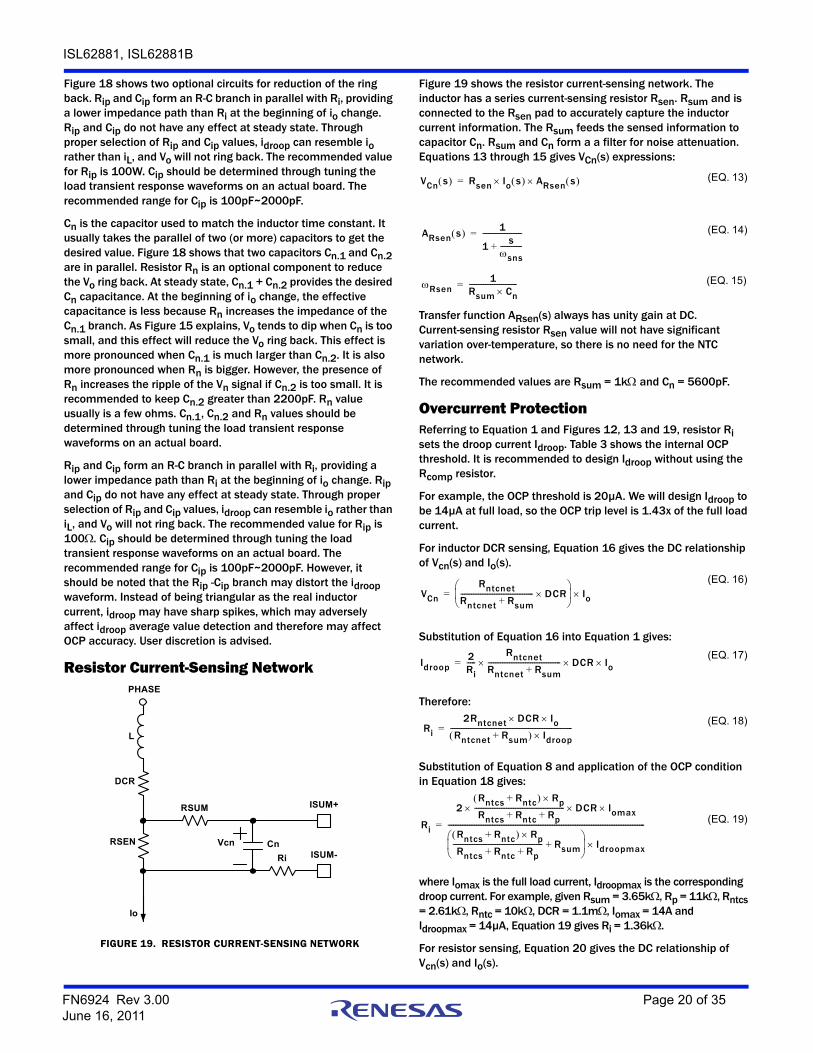
Figure 19 shows the resistor current-sensing network. The inductor has a series current-sensing resistor Rsen. Rsum and is connected to the Rsen pad to accurately capture the inductor current information. The Rsum feeds the sensed information to capacitor Cn. Rsum and Cn form a a filter for noise attenuation. Equations 13 through 15 gives VCn(s) expressions:
Transfer function ARsen(s) always has unity gain at DC. Current-sensing resistor Rsen value will not have significant variation over-temperature, so there is no need for the NTC network.
The recommended values are Rsum = 1k and Cn = 5600pF.
Overcurrent ProtectionReferring to Equation 1 and Figures 12, 13 and 19, resistor Ri sets the droop current Idroop. Table 3 shows the internal OCP threshold. It is recommended to design Idroop without using the Rcomp resistor.
For example, the OCP threshold is 20µA. We will design Idroop to be 14µA at full load, so the OCP trip level is 1.43x of the full load current.
For inductor DCR sensing, Equation 16 gives the DC relationship of Vcn(s) and Io(s).
Substitution of Equation 16 into Equation 1 gives:
Therefore:
Substitution of Equation 8 and application of the OCP condition in Equation 18 gives:
where Iomax is the full load current, Idroopmax is the corresponding droop current. For example, given Rsum = 3.65k, Rp = 11k, Rntcs = 2.61k, Rntc = 10k, DCR = 1.1m, Iomax = 14A and Idroopmax = 14µA, Equation 19 gives Ri = 1.36k.
For resistor sensing, Equation 20 gives the DC relationship of Vcn(s) and Io(s).
Cn
RSUM
DCR
L
PHASE
Io
Ri
ISUM+
ISUM-VcnRSEN
FIGURE 19. RESISTOR CURRENT-SENSING NETWORK
VCn s Rsen Io s ARsen s = (EQ. 13)
ARsen s 1
1s
sns------------+
----------------------= (EQ. 14)
Rsen1
Rsum Cn---------------------------= (EQ. 15)
VCn
RntcnetRntcnet Rsum+----------------------------------------- DCR
Io=(EQ. 16)
Idroop2Ri-----
RntcnetRntcnet Rsum+----------------------------------------- DCR Io=
(EQ. 17)
Ri
2Rntcnet DCR Io
Rntcnet Rsum+ Idroop---------------------------------------------------------------------=
(EQ. 18)
Ri
2Rntcs Rntc+ Rp
Rntcs Rntc Rp+ +--------------------------------------------------- DCR Iomax
Rntcs Rntc+ Rp
Rntcs Rntc Rp+ +--------------------------------------------------- Rsum+
Idroopmax
---------------------------------------------------------------------------------------------------------------= (EQ. 19)
FN6924 Rev 3.00 Page 20 of 35June 16, 2011
ISL62881, ISL62881B
Substitution of Equation 20 into Equation 1 gives Equation 21:
Therefore:
Substitution of Equation 22 and application of the OCP condition in Equation 18 gives:
where Iomax is the full load current, Idroopmax is the corresponding droop current. For example, given Rsen = 1m, Iomax = 14A and Idroopmax = 14µA, Equation 23 gives Ri = 2k.
A resistor from COMP to GND can adjust the internal OCP threshold, providing another dimension of fine-tune flexibility. Table 3 shows the detail. It is recommended to scale Idroop such that the default OCP threshold gives approximately the desired OCP level, then use Rcomp to fine tune the OCP level if necessary.
Load Line SlopeRefer to Figure 12.
For inductor DCR sensing, substitution of Equation 17 into Equation 2 gives the load line slope expression in Equation 24.
For resistor sensing, substitution of Equation 21 into Equation 2 gives the load line slope expression in Equation 25:
Substitution of Equation 18 and rewriting Equation 24, or substitution of Equation 22 and rewriting Equation 25 gives the same result in Equation 26:
One can use the full load condition to calculate Rdroop. For example, given Iomax = 14A, Idroopmax = 14µA and LL = 7m, Equation 26 gives Rdroop = 7k.
It is recommended to start with the Rdroop value calculated by Equation 26, and fine tune it on the actual board to get accurate load line slope. One should record the output voltage readings at no load and at full load for load line slope calculation. Reading the output voltage at lighter load instead of full load will increase the measurement error.
Current MonitorReferring to Equation 6 for the IMON pin current expression.
Refer to Figures 1 and 2, the IMON pin current flows through Rimon. The voltage across Rimon is shown in Equation 27:
Rewriting Equation 26 gives Equation 28:
Substitution of Equation 28 into Equation 27 gives Equation 29:
Rewriting Equation 29 and application of full load condition gives Equation 30:
For example, given LL = 7m, Rdroop = 7k, VRimon = 963mV at Iomax = 14A, Equation 30 gives Rimon = 22.9k.
A capacitor Cimon can be paralleled with Rimon to filter the IMON pin voltage. The RimonCimon time constant is the user’s choice. It is recommended to have a time constant long enough such that switching frequency ripples are removed.
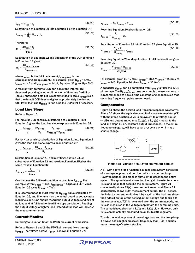
CompensatorFigure 14 shows the desired load transient response waveforms. Figure 20 shows the equivalent circuit of a voltage regulator (VR) with the droop function. A VR is equivalent to a voltage source (= VID) and output impedance Zout(s). If Zout(s) is equal to the load line slope LL, i.e. constant output impedance, in the entire frequency range, Vo will have square response when Io has a square change.
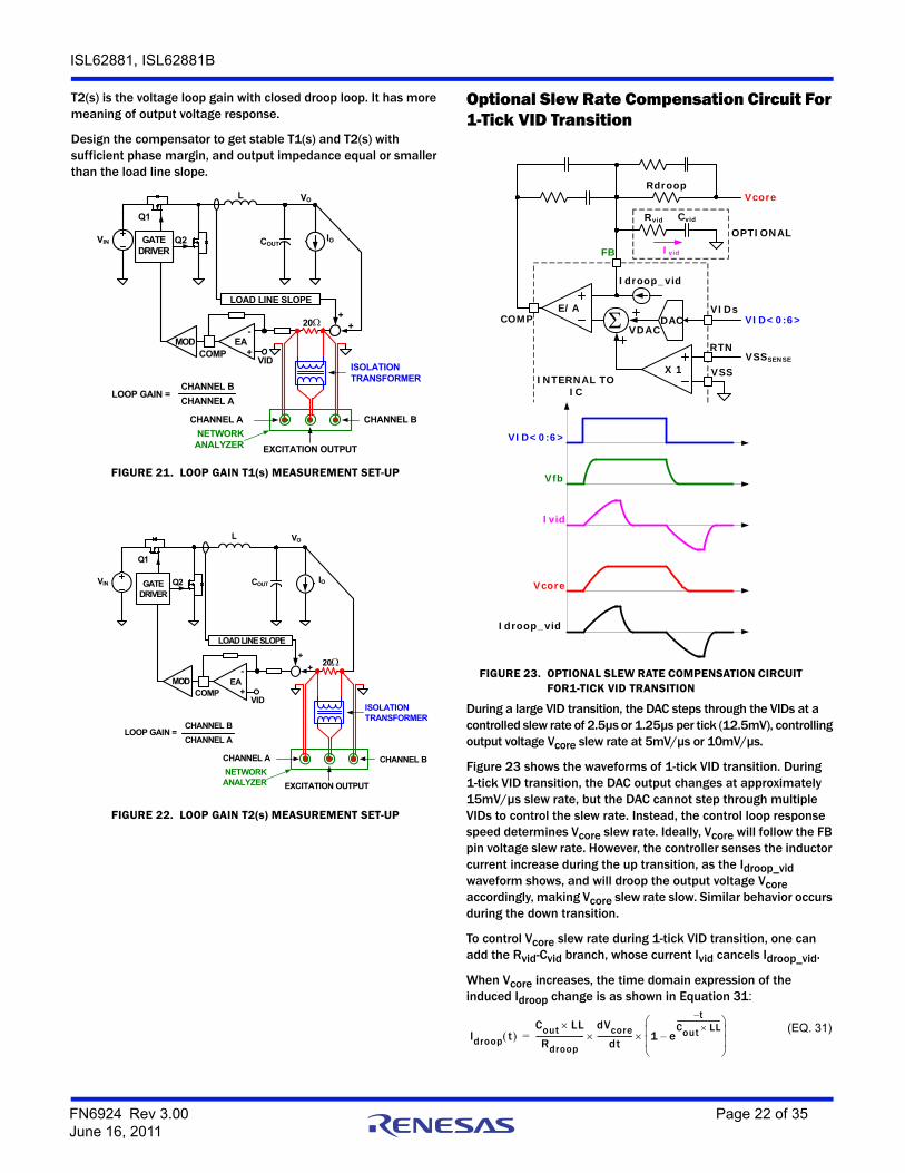
A VR with active droop function is a dual-loop system consisting of a voltage loop and a droop loop which is a current loop. However, neither loop alone is sufficient to describe the entire system. The spreadsheet shows two loop gain transfer functions, T1(s) and T2(s), that describe the entire system. Figure 21 conceptually shows T1(s) measurement set-up and Figure 22 conceptually shows T2(s) measurement set-up. The VR senses the inductor current, multiplies it by a gain of the load line slope, then adds it on top of the sensed output voltage and feeds it to the compensator. T(1) is measured after the summing node, and T2(s) is measured in the voltage loop before the summing node. The spreadsheet gives both T1(s) and T2(s) plots. However, only T2(s) can be actually measured on an ISL62881 regulator.
T1(s) is the total loop gain of the voltage loop and the droop loop. It always has a higher crossover frequency than T2(s) and has more meaning of system stability.
VCn Rsen Io= (EQ. 20)
Idroop2Ri----- Rsen Io= (EQ. 21)
Ri
2Rsen Io
Idroop---------------------------=
(EQ. 22)
Ri
2Rsen Iomax
Idroopmax--------------------------------------=
(EQ. 23)
LLVdroop
Io------------------
2RdroopRi
----------------------Rntcnet
Rntcnet Rsum+----------------------------------------- DCR= =
(EQ. 24)
LLVdroop
Io------------------
2Rsen Rdroop
Ri-----------------------------------------= =
(EQ. 25)
Rdroop
IoIdroop---------------- LL= (EQ. 26)
VRimon 3 I droop Rimon= (EQ. 27)
Idroop
IoRdroop------------------ LL=
(EQ. 28)
VRimon
3Io LL
Rdroop--------------------- Rimon=
(EQ. 29)
Rimon
VRimon Rdroop
3Io LL--------------------------------------------=
(EQ. 30)
FIGURE 20. VOLTAGE REGULATOR EQUIVALENT CIRCUIT
iO
VOVID
Zout(s) = LL
LOADVR +
-
FN6924 Rev 3.00 Page 21 of 35June 16, 2011
ISL62881, ISL62881B
T2(s) is the voltage loop gain with closed droop loop. It has more meaning of output voltage response.
Design the compensator to get stable T1(s) and T2(s) with sufficient phase margin, and output impedance equal or smaller than the load line slope.
Optional Slew Rate Compensation Circuit For 1-Tick VID Transition
During a large VID transition, the DAC steps through the VIDs at a controlled slew rate of 2.5µs or 1.25µs per tick (12.5mV), controlling output voltage Vcore slew rate at 5mV/µs or 10mV/µs.
Figure 23 shows the waveforms of 1-tick VID transition. During 1-tick VID transition, the DAC output changes at approximately 15mV/µs slew rate, but the DAC cannot step through multiple VIDs to control the slew rate. Instead, the control loop response speed determines Vcore slew rate. Ideally, Vcore will follow the FB pin voltage slew rate. However, the controller senses the inductor current increase during the up transition, as the Idroop_vid waveform shows, and will droop the output voltage Vcore accordingly, making Vcore slew rate slow. Similar behavior occurs during the down transition.
To control Vcore slew rate during 1-tick VID transition, one can add the Rvid-Cvid branch, whose current Ivid cancels Idroop_vid.
When Vcore increases, the time domain expression of the induced Idroop change is as shown in Equation 31:
FIGURE 21. LOOP GAIN T1(s) MEASUREMENT SET-UP
Q2
Q1
L
IOCOUT
VO
VIN GATE DRIVER
COMPMOD
LOAD LINE SLOPE
EA
VID
CHANNEL BCHANNEL A
EXCITATION OUTPUT
ISOLATION TRANSFORMER
20
LOOP GAIN =CHANNEL B
CHANNEL A
NETWORK ANALYZER
+
-
++
FIGURE 22. LOOP GAIN T2(s) MEASUREMENT SET-UP
Q2
Q1
L
IOCOUT
VO
VIN GATE DRIVER
COMPMOD
LOAD LINE SLOPE
EA
VID
CHANNEL BCHANNEL A
EXCITATION OUTPUT
ISOLATION TRANSFORMER
20
LOOP GAIN =CHANNEL B
CHANNEL A
NETWORK ANALYZER
+
+
+
-
FIGURE 23. OPTIONAL SLEW RATE COMPENSATION CIRCUIT FOR1-TICK VID TRANSITION
X 1
E/A DAC VID<0:6>
Rdroop
Idroop_vid
VDAC
FB
COMP
Vcore
VSSSENSE
VIDs
RTN
VSSINTERNAL TO
IC
Rvid Cvid
VID<0:6>
Vfb
Vcore
Ivid
Idroop_vid
Ivid
OPTIONAL
Idroop t Cout LL
Rdroop------------------------
dVcoredt
------------------ 1 e
t–Cout LL-------------------------
–
=(EQ. 31)
FN6924 Rev 3.00 Page 22 of 35June 16, 2011
ISL62881, ISL62881B
where Cout is the total output capacitance.
In the meantime, the Rvid-Cvid branch current Ivid time domain expression is as shown in Equation 32:
It is desired to let Ivid(t) cancel Idroop_vid(t). So there are:
and:
The result is:
and:
For example: given LL = 3m, Rdroop = 4.22k, Cout = 1320µF, dVcore/dt = 5mV/µs and dVfb/dt = 15mV/µs, Equation 35 gives Rvid = 4.22k and Equation 36 gives Cvid = 227pF.
It’s recommended to select the calculated Rvid value and start with the calculated Cvid value and tweak it on the actual board to get the best performance.
During normal transient response, the FB pin voltage is held constant, therefore is virtual ground in small signal sense. The Rvid-Cvid network is between the virtual ground and the real ground, and hence has no affect on transient response.
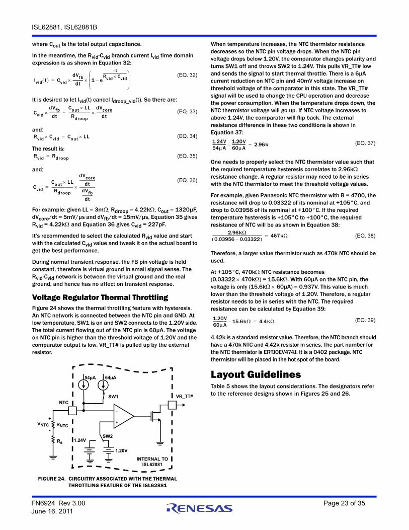
Voltage Regulator Thermal ThrottlingFigure 24 shows the thermal throttling feature with hysteresis. An NTC network is connected between the NTC pin and GND. At low temperature, SW1 is on and SW2 connects to the 1.20V side. The total current flowing out of the NTC pin is 60µA. The voltage on NTC pin is higher than the threshold voltage of 1.20V and the comparator output is low. VR_TT# is pulled up by the external resistor.
When temperature increases, the NTC thermistor resistance decreases so the NTC pin voltage drops. When the NTC pin voltage drops below 1.20V, the comparator changes polarity and turns SW1 off and throws SW2 to 1.24V. This pulls VR_TT# low and sends the signal to start thermal throttle. There is a 6µA current reduction on NTC pin and 40mV voltage increase on threshold voltage of the comparator in this state. The VR_TT# signal will be used to change the CPU operation and decrease the power consumption. When the temperature drops down, the NTC thermistor voltage will go up. If NTC voltage increases to above 1.24V, the comparator will flip back. The external resistance difference in these two conditions is shown in Equation 37:
One needs to properly select the NTC thermistor value such that the required temperature hysteresis correlates to 2.96k resistance change. A regular resistor may need to be in series with the NTC thermistor to meet the threshold voltage values.
For example, given Panasonic NTC thermistor with B = 4700, the resistance will drop to 0.03322 of its nominal at +105°C, and drop to 0.03956 of its nominal at +100°C. If the required temperature hysteresis is +105°C to +100°C, the required resistance of NTC will be as shown in Equation 38:
Therefore, a larger value thermistor such as 470k NTC should be used.
At +105°C, 470k NTC resistance becomes (0.03322 470k) = 15.6k. With 60µA on the NTC pin, the voltage is only (15.6k60µA) = 0.937V. This value is much lower than the threshold voltage of 1.20V. Therefore, a regular resistor needs to be in series with the NTC. The required resistance can be calculated by Equation 39:
4.42k is a standard resistor value. Therefore, the NTC branch should have a 470k NTC and 4.42k resistor in series. The part number for the NTC thermistor is ERTJ0EV474J. It is a 0402 package. NTC thermistor will be placed in the hot spot of the board.
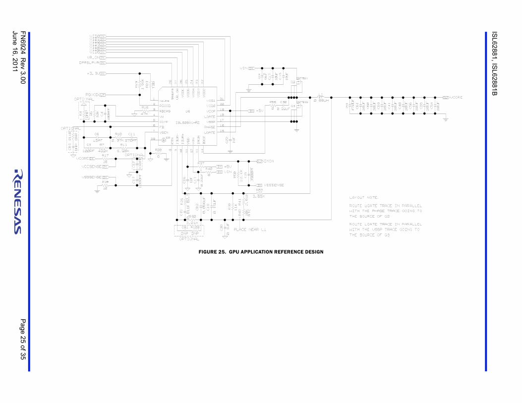
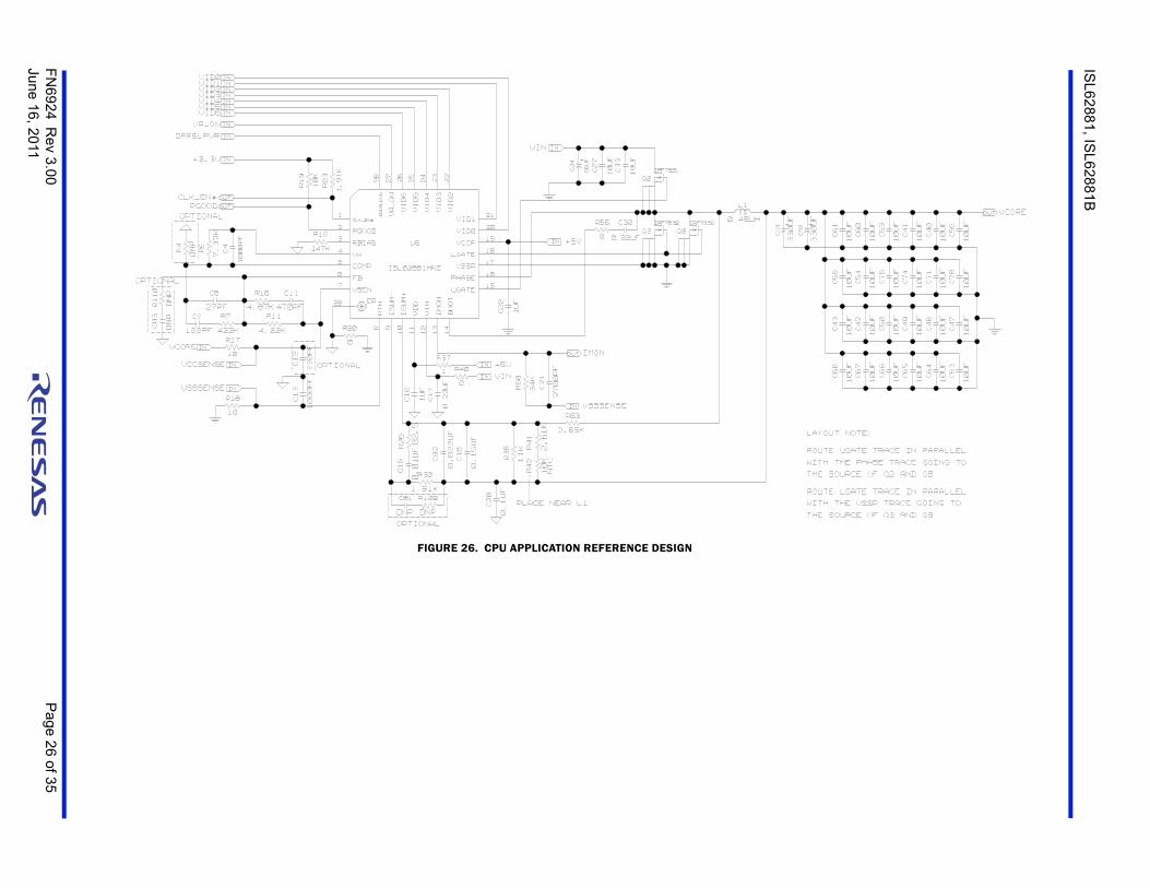
Layout GuidelinesTable 5 shows the layout considerations. The designators refer to the reference designs shown in Figures 25 and 26.
Ivid t Cvid
dVfbdt------------ 1 e
t–Rvid Cvid------------------------------
–
=(EQ. 32)
Cvid
dVfbdt------------
Cout LL
Rdroop------------------------
dVcoredt
------------------= (EQ. 33)
Rvid Cvid Cout LL= (EQ. 34)
Rvid Rdroop= (EQ. 35)
Cvid
Cout LL
Rdroop------------------------
dVcoredt
------------------
dVfbdt------------
------------------=(EQ. 36)
NTC
RNTC
-
+VNTC-
+
VR_TT#
1.24V
54µA
INTERNAL TOISL62881
FIGURE 24. CIRCUITRY ASSOCIATED WITH THE THERMAL THROTTLING FEATURE OF THE ISL62881
Rs
64µA
1.20V
SW1
SW2
1.24V54A--------------- 1.20V
60A---------------– 2.96k= (EQ. 37)
(EQ. 38)2.96k
0.03956 0.03322– ------------------------------------------------------- 467k=
(EQ. 39)1.20V60A--------------- 15.6k– 4.4k=
FN6924 Rev 3.00 Page 23 of 35June 16, 2011
ISL62881, ISL62881B
TABLE 5. LAYOUT CONSIDERATIONS
NAME LAYOUT CONSIDERATION
GND Create analog ground plane underneath the controller and the analog signal processing components. Don’t let the power ground plane overlap with the analog ground plane. Avoid noisy planes/traces (e.g.: phase node) from crossing over/overlapping with the analog plane.
CLK_EN# No special consideration.
PGOOD No special consideration.
RBIAS Place the RBIAS resistor (R16) in general proximity of the controller. Low impedance connection to the analog ground plane.
VR_TT# No special consideration.
NTC The NTC thermistor (R9) needs to be placed close to the thermal source that is monitor to determine thermal throttling. Usually it’s placed close to phase-1 high-side MOSFET.
VW Place capacitor (C4) across VW and COMP in close proximity of the controller.
COMP Place compensator components (C3, C5, C6 R7, R11, R10 and C11) in general proximity of the controller.
FB
VSEN Place the VSEN/RTN filter (C12, C13) in close proximity of the controller for good decoupling.
RTN
VDD A capacitor (C16) decouples it to GND. Place it in close proximity of the controller.
IMON Place the filter capacitor (C21) close to the CPU.
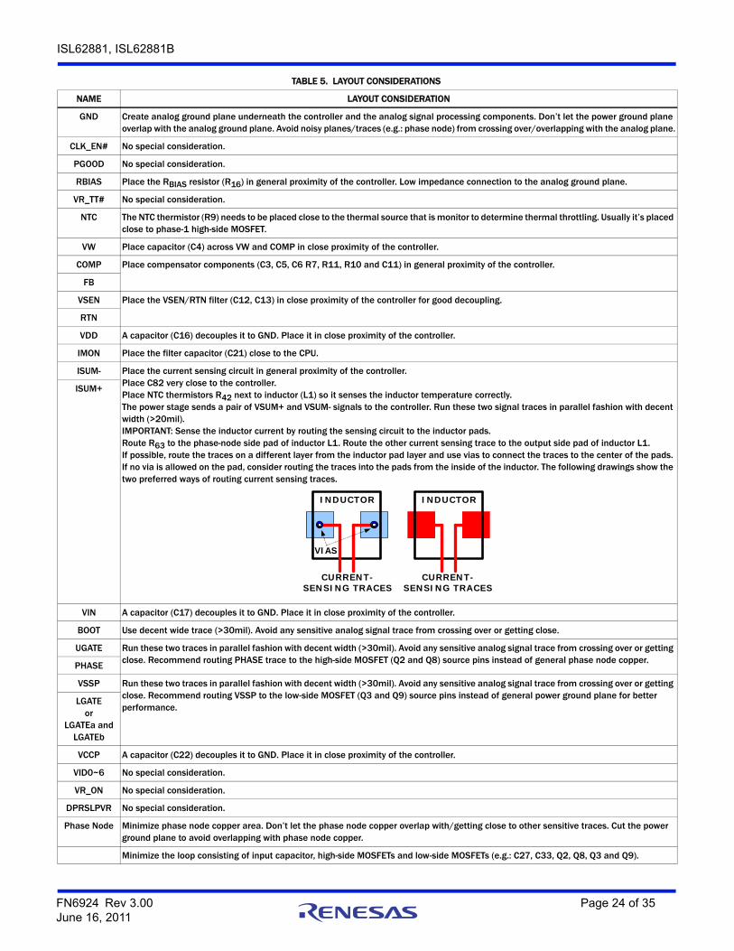
ISUM- Place the current sensing circuit in general proximity of the controller. Place C82 very close to the controller. Place NTC thermistors R42 next to inductor (L1) so it senses the inductor temperature correctly. The power stage sends a pair of VSUM+ and VSUM- signals to the controller. Run these two signal traces in parallel fashion with decent width (>20mil).IMPORTANT: Sense the inductor current by routing the sensing circuit to the inductor pads. Route R63 to the phase-node side pad of inductor L1. Route the other current sensing trace to the output side pad of inductor L1.If possible, route the traces on a different layer from the inductor pad layer and use vias to connect the traces to the center of the pads. If no via is allowed on the pad, consider routing the traces into the pads from the inside of the inductor. The following drawings show the two preferred ways of routing current sensing traces.
ISUM+
VIN A capacitor (C17) decouples it to GND. Place it in close proximity of the controller.
BOOT Use decent wide trace (>30mil). Avoid any sensitive analog signal trace from crossing over or getting close.
UGATE Run these two traces in parallel fashion with decent width (>30mil). Avoid any sensitive analog signal trace from crossing over or getting close. Recommend routing PHASE trace to the high-side MOSFET (Q2 and Q8) source pins instead of general phase node copper.
PHASE
VSSP Run these two traces in parallel fashion with decent width (>30mil). Avoid any sensitive analog signal trace from crossing over or getting close. Recommend routing VSSP to the low-side MOSFET (Q3 and Q9) source pins instead of general power ground plane for better performance.
LGATEor
LGATEa andLGATEb
VCCP A capacitor (C22) decouples it to GND. Place it in close proximity of the controller.
VID0~6 No special consideration.
VR_ON No special consideration.
DPRSLPVR No special consideration.
Phase Node Minimize phase node copper area. Don’t let the phase node copper overlap with/getting close to other sensitive traces. Cut the power ground plane to avoid overlapping with phase node copper.
Minimize the loop consisting of input capacitor, high-side MOSFETs and low-side MOSFETs (e.g.: C27, C33, Q2, Q8, Q3 and Q9).
INDUCTOR
CURRENT-SENSING TRACES
VIAS
INDUCTOR
CURRENT-SENSING TRACES
FN6924 Rev 3.00 Page 24 of 35June 16, 2011
FN
692
4R
ev 3
.00
Pa
ge 2
5 of 35
June 16, 2011
ISL6
288
1, ISL
628
81B
TRACE IN PARALLELSE TRACE GOING TOF Q2
TRACE IN PARALLELP TRACE GOING TOF Q3
10UF
10UF
10UF
10UF
10UF
10UF
C54
VCORE
C41
C40
C56
C55
C59
OUT
3900PF
PLACE NEAR L1------------
OPTIONAL
----
DNP
DNP
--------
----
OPTIONAL
-------
----
270PF
470UF
DNP
TBD
----
-------
----
OPTIONAL
----
-----
422K
----
DNP ----
------------
330PF
2.37K
6.98K
DNP
0.15UF
0.88UH
15PF
47K
0.1UF
----->0.
01UF 11K
NTC
10K
2.61K
22.6K
3.65K
IRF7832
IRF7821
LAYOUT NOTE:
82.5
3.01K
0.056UF
OPTIONAL
-----
ROUTE UGATE
10K
WITH THE PHATHE SOURCE O
ROUTE LGATEWITH THE VSSTHE SOURCE O
1000PF
100PF--------
10UF
10UF
C11
R23
1.91
K
R19 26
ISL62881HRZ
C12
VCCSENSE
R20
C81 R109
L1
R56
C6
C16
R10
R11
C15
0.22UF
C3
VSSSENSE
VCORE
+5V
VR_ON
VID2
VID6VID5VID3VID1VID0
VIN
10
R17
R7
C4
0
18
22
16
8 9
21
U6
2428
19
17
3
4
1
5
6
7
10 11 12 13 14
15
202
R30
C20
R26
C82
1UF
C17
1VIN
R38
R42
R41
R63
R50
C21
VID4
0
C30
0.22UF
56UF
C24
10UF
C27
10UF
C33
Q3
Q2
C61
C60
C52
10
1000PF
23
29
R16
R6
C22
1UF
0
R40
R37
27
+5V
R18
R4
C13
25
DPRSLPVR
+3.3V
PGOOD
R110
C83
C18
VSSSENSE
IMON
EP
VID6
VID5
VID4
DPRS
LPVR
VCCP
LGATE
VSSP
VR_ON
RBIAS
VW
CLK_EN#
COMP
FB
VSEN
RTN
ISUM
-IS
UM+
VDD
VIN
IMON
BOOT
UGATE
PHASE
VID0
VID1
VID2
VID3
PGOOD
OUT
IN
IN
IN
IN IN
IN
IN
OUT
IN
IN
IN
IN
IN
ININ
IN
IN
IN
IN
FIGURE 25. GPU APPLICATION REFERENCE DESIGN
FN
692
4R
ev 3
.00
Pa
ge 2
6 of 35
June 16, 2011
ISL6
288
1, ISL
628
81B
THE VSSP TRACE GOING TO
UGATE TRACE IN PARALLEL
10UF
10UF
OURCE OF Q2 AND Q8
OURCE OF Q3 AND Q9
LGATE TRACE IN PARALLEL
10UF
10UF
10UF
10UF
10UF
10UF
10UF
10UF
10UF
10UF
10UF
10UF
10UF
10UF
10UF
10UF
10UF
10UF
10UF
10UF
10UF
NOTE:
THE PHASE TRACE GOING TO
10UF
C60
C67
VCORE
C68
C66
C65
C64
C43
C42
C50
C55
C54
C61
C75
C59
C49
C48
C74
C41
C71
C40
C63
C47
C70
C56
OUT
2700PF
WITH
ROUTE
THE S
THE S----
-----------
0.01UF
OPTIONAL
----
-------
OPTIONAL
----
-----
DNPDNP
1.91K
-----------
82.5
0.022UF
-----
----
1000PF
IRF7821
ROUTE
LAYOUT
WITH
330UF
330UF
4.87K
----->
11K
0.1UF
10K
NTC
IRF7832 IRF7832 0.45UH
3.65K
2.61K
34K
4.22K
470PF27PF
100PF 422K
330PF
PLACE NEAR L1
0.15UF
----7.32K
DNP
DNP
DNP
-------
----
----
----
--------
--------
OPTIONAL
OPTIONALC11
18
19
14
R37
C17
R110
C83
C13
R4
C30
+3.3V
VSSSENSE
R41
Q3
R30
C82
R11
CLK_EN#
1.91
K
R23
PGOOD
10K
R19
VID0VID2
C81 R109
0.22UF
13
ISL62881HRZ
1UF
15
16
0
1
R17
C3
C4R6
C52
0.22UF
C24
C27
+5V
C16
VIN
56UF
0
10UF
C33
10UF
Q9
1UF
C22
VID1VID3VID5VID6
VR_ONDPRSLPVR
VID4
R16
147K
R10
2
23
20
10
7
5
1
29
4
3
17
28 25
U6
0
C21
R50
R40 +5V
21
98R20
22
R42
C20
L1
Q2
C39
VCORE
2627
R38
R56
R63VSSSENSE
VCCSENSEVIN
IMON
1211
C18
10
1000PF
C12
C6
R18
R7
R26
C15
24
6
10
EP
VID6
VID5
VID4
DPRS
LPVR
VCCP
LGATE
VSSP
VR_ON
RBIAS
VW
CLK_EN#
COMP
FB
VSEN
RTN
ISUM
-IS
UM+
VDD
VIN
IMON
BOOT
UGATE
PHASE
VID0
VID1
VID2
VID3
PGOOD
IN
IN
IN
IN
IN
IN
IN
OUT
IN
IN
IN
IN
IN
ININ
IN
IN
IN
OUT
IN
OUT
FIGURE 26. CPU APPLICATION REFERENCE DESIGN
ISL62881, ISL62881B
CPU Application Reference Design Bill of MaterialsQTY REFERENCE VALUE DESCRIPTION MANUFACTURER PART NUMBER PACKAGE
1 C11 470pF Multilayer Cap, 16V, 10% GENERIC H1045-00471-16V10 SM0603
1 C12 330pF Multilayer Cap, 16V, 10% GENERIC H1045-00331-16V10 SM0603
1 C13 1000pF Multilayer Cap, 16V, 10% GENERIC H1045-00102-16V10 SM0603
1 C15 0.01µF Multilayer Cap, 16V, 10% GENERIC H1045-00103-16V10 SM0603
2 C16, C22 1µF Multilayer Cap, 16V, 20% GENERIC H1045-00105-16V20 SM0603
1 C18 0.15µF Multilayer Cap, 16V, 10% GENERIC H1045-00154-16V10 SM0603
1 C20 0.1µF Multilayer Cap, 16V, 10% GENERIC H1045-00104-16V10 SM0603
1 C21 2700pF Multilayer Cap, 16V, 10% GENERIC H1045-00272-16V10 SM0603
2 C17, C30 0.22µF Multilayer Cap, 25V, 10% GENERIC H1045-00224-25V10 SM0603
1 C24 56µF Radial SP Series Cap, 25V, 20% SANYO 25SP56M CASE-CC
2 C27, C33 10µF Multilayer Cap, 25V, 20% GENERIC H1065-00106-25V20 SM1206
1 C3 100pF Multilayer Cap, 16V, 10% GENERIC H1045-00101-16V10 SM0603
2 C39, C52 330µF SPCAP, 2V, 4M PANASONIC EEXSX0D331E4
POLYMER CAP, 2.5V, 4.5M KEMET T520V337M2R5A(1)E4R5-6666
1 C4 1000pF Multilayer Cap, 16V, 10% GENERIC H1045-00102-16V10 SM0603
30 C40-C43, C47-C50,
C53-C56, C59, C75, C78
10µF Multilayer Cap, 6.3V, 20% MURATA GRM21BR61C106KE15L SM0805
TDK C2012X5R0J106K
1 C6 27pF Multilayer Cap, 16V, 10% GENERIC H1045-00270-16V10 SM0603
1 C82 0.022µF Multilayer Cap, 16V, 10% GENERIC H1045-00223-16V10 SM0603
0 C81, C83 DNP
1 L1 0.45µH Inductor, Inductance 20%, DCR 7% NEC-TOKIN MPCG1040LR45 10mmx10mm
1 Q2 N-Channel Power MOSFET IR IRF7821 PWRPAKSO8
2 Q3, Q9 N-Channel Power MOSFET IR IRF7832 PWRPAKSO8
1 R10 4.87k Thick Film Chip Resistor, 1% GENERIC H2511-04871-1/16W1 SM0603
1 R11 4.22k Thick Film Chip Resistor, 1% GENERIC H2511-04221-1/16W1 SM0603
1 R16 147k Thick Film Chip Resistor, 1% GENERIC H2511-01473-1/16W1 SM0603
2 R17, R18 10 Thick Film Chip Resistor, 1% GENERIC H2511-00100-1/16W1 SM0603
1 R19 1.91k Thick Film Chip Resistor, 1% GENERIC H2511-01911-1/16W1 SM0603
1 R26 82.5 Thick Film Chip Resistor, 1% GENERIC H2511-082R5-1/16W1 SM0603
3 R20, R40, R56 0 Thick Film Chip Resistor, 1% GENERIC H2511-00R00-1/16W1 SM0603
1 R30 1.91k Thick Film Chip Resistor, 1% GENERIC H2511-01911-1/16W1 SM0603
1 R37 1 Thick Film Chip Resistor, 1% GENERIC H2511-01R00-1/16W1 SM0603
1 R38 11k Thick Film Chip Resistor, 1% GENERIC H2511-01102-1/16W1 SM0603
1 R41 2.61k Thick Film Chip Resistor, 1% GENERIC H2511-02611-1/16W1 SM0603
1 R42 10k NTC Thermistor, 10k NTC PANASONIC ERT-J1VR103J SM0603
1 R50 34k Thick Film Chip Resistor, 1% GENERIC H2511-03402-1/16W1 SM0603
FN6924 Rev 3.00 Page 27 of 35June 16, 2011
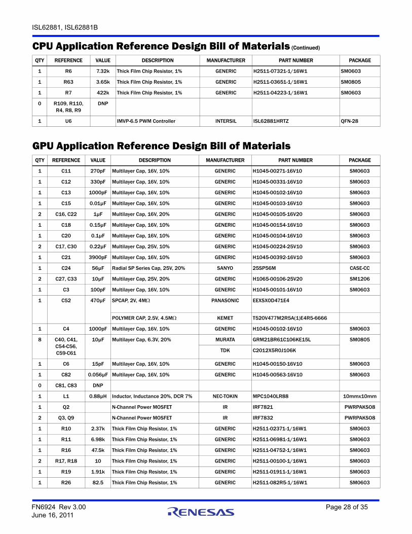
ISL62881, ISL62881B
1 R6 7.32k Thick Film Chip Resistor, 1% GENERIC H2511-07321-1/16W1 SM0603
1 R63 3.65k Thick Film Chip Resistor, 1% GENERIC H2511-03651-1/16W1 SM0805
1 R7 422k Thick Film Chip Resistor, 1% GENERIC H2511-04223-1/16W1 SM0603
0 R109, R110, R4, R8, R9
DNP
1 U6 IMVP-6.5 PWM Controller INTERSIL ISL62881HRTZ QFN-28
CPU Application Reference Design Bill of Materials (Continued)
QTY REFERENCE VALUE DESCRIPTION MANUFACTURER PART NUMBER PACKAGE
GPU Application Reference Design Bill of MaterialsQTY REFERENCE VALUE DESCRIPTION MANUFACTURER PART NUMBER PACKAGE
1 C11 270pF Multilayer Cap, 16V, 10% GENERIC H1045-00271-16V10 SM0603
1 C12 330pF Multilayer Cap, 16V, 10% GENERIC H1045-00331-16V10 SM0603
1 C13 1000pF Multilayer Cap, 16V, 10% GENERIC H1045-00102-16V10 SM0603
1 C15 0.01µF Multilayer Cap, 16V, 10% GENERIC H1045-00103-16V10 SM0603
2 C16, C22 1µF Multilayer Cap, 16V, 20% GENERIC H1045-00105-16V20 SM0603
1 C18 0.15µF Multilayer Cap, 16V, 10% GENERIC H1045-00154-16V10 SM0603
1 C20 0.1µF Multilayer Cap, 16V, 10% GENERIC H1045-00104-16V10 SM0603
2 C17, C30 0.22µF Multilayer Cap, 25V, 10% GENERIC H1045-00224-25V10 SM0603
1 C21 3900pF Multilayer Cap, 16V, 10% GENERIC H1045-00392-16V10 SM0603
1 C24 56µF Radial SP Series Cap, 25V, 20% SANYO 25SP56M CASE-CC
2 C27, C33 10µF Multilayer Cap, 25V, 20% GENERIC H1065-00106-25V20 SM1206
1 C3 100pF Multilayer Cap, 16V, 10% GENERIC H1045-00101-16V10 SM0603
1 C52 470µF SPCAP, 2V, 4M PANASONIC EEXSX0D471E4
POLYMER CAP, 2.5V, 4.5M KEMET T520V477M2R5A(1)E4R5-6666
1 C4 1000pF Multilayer Cap, 16V, 10% GENERIC H1045-00102-16V10 SM0603
8 C40, C41, C54-C56,C59-C61
10µF Multilayer Cap, 6.3V, 20% MURATA GRM21BR61C106KE15L SM0805
TDK C2012X5R0J106K
1 C6 15pF Multilayer Cap, 16V, 10% GENERIC H1045-00150-16V10 SM0603
1 C82 0.056µF Multilayer Cap, 16V, 10% GENERIC H1045-00563-16V10 SM0603
0 C81, C83 DNP
1 L1 0.88µH Inductor, Inductance 20%, DCR 7% NEC-TOKIN MPC1040LR88 10mmx10mm
1 Q2 N-Channel Power MOSFET IR IRF7821 PWRPAKSO8
2 Q3, Q9 N-Channel Power MOSFET IR IRF7832 PWRPAKSO8
1 R10 2.37k Thick Film Chip Resistor, 1% GENERIC H2511-02371-1/16W1 SM0603
1 R11 6.98k Thick Film Chip Resistor, 1% GENERIC H2511-06981-1/16W1 SM0603
1 R16 47.5k Thick Film Chip Resistor, 1% GENERIC H2511-04752-1/16W1 SM0603
2 R17, R18 10 Thick Film Chip Resistor, 1% GENERIC H2511-00100-1/16W1 SM0603
1 R19 1.91k Thick Film Chip Resistor, 1% GENERIC H2511-01911-1/16W1 SM0603
1 R26 82.5 Thick Film Chip Resistor, 1% GENERIC H2511-082R5-1/16W1 SM0603
FN6924 Rev 3.00 Page 28 of 35June 16, 2011
ISL62881, ISL62881B
3 R20, R40, R56 0 Thick Film Chip Resistor, 1% GENERIC H2511-00R00-1/16W1 SM0603
1 R30 3.01k Thick Film Chip Resistor, 1% GENERIC H2511-03011-1/16W1 SM0603
1 R37 1 Thick Film Chip Resistor, 1% GENERIC H2511-01R00-1/16W1 SM0603
1 R38 11k Thick Film Chip Resistor, 1% GENERIC H2511-01102-1/16W1 SM0603
1 R41 2.61k Thick Film Chip Resistor, 1% GENERIC H2511-02611-1/16W1 SM0603
1 R42 10k NTC Thermistor, 10k NTC PANASONIC ERT-J1VR103J SM0603
1 R50 22.6k Thick Film Chip Resistor, 1% GENERIC H2511-02262-1/16W1 SM0603
1 R6 10k Thick Film Chip Resistor, 1% GENERIC H2511-01002-1/16W1 SM0603
1 R63 3.65k Thick Film Chip Resistor, 1% GENERIC H2511-03651-1/16W1 SM0805
1 R7 412k Thick Film Chip Resistor, 1% GENERIC H2511-04123-1/16W1 SM0603
0 R109, R110,R4, R8, R9
DNP
1 U6 IMVP-6.5 PWM Controller INTERSIL ISL62881HRTZ QFN-28
GPU Application Reference Design Bill of Materials (Continued)
QTY REFERENCE VALUE DESCRIPTION MANUFACTURER PART NUMBER PACKAGE
FN6924 Rev 3.00 Page 29 of 35June 16, 2011
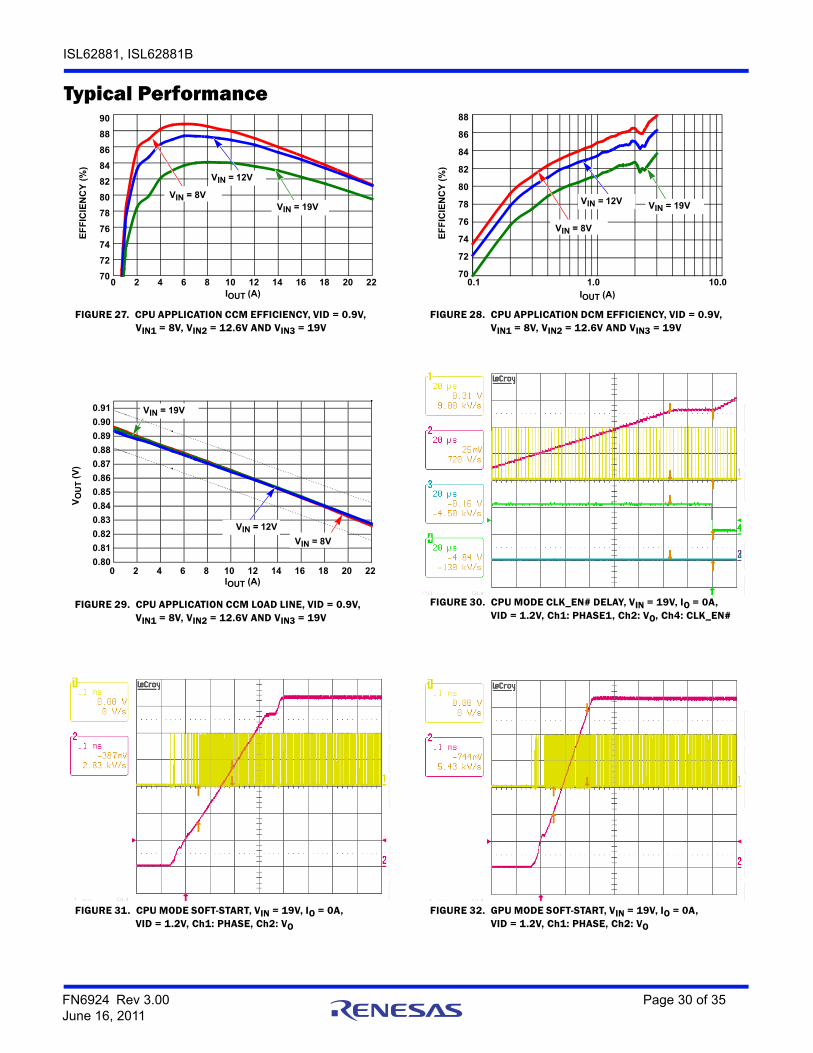
ISL62881, ISL62881B
Typical Performance
FIGURE 27. CPU APPLICATION CCM EFFICIENCY, VID = 0.9V, VIN1 = 8V, VIN2 = 12.6V AND VIN3 = 19V
FIGURE 28. CPU APPLICATION DCM EFFICIENCY, VID = 0.9V, VIN1 = 8V, VIN2 = 12.6V AND VIN3 = 19V
FIGURE 29. CPU APPLICATION CCM LOAD LINE, VID = 0.9V, VIN1 = 8V, VIN2 = 12.6V AND VIN3 = 19V
FIGURE 30. CPU MODE CLK_EN# DELAY, VIN = 19V, IO = 0A, VID = 1.2V, Ch1: PHASE1, Ch2: VO, Ch4: CLK_EN#
FIGURE 31. CPU MODE SOFT-START, VIN = 19V, IO = 0A, VID = 1.2V, Ch1: PHASE, Ch2: VO
FIGURE 32. GPU MODE SOFT-START, VIN = 19V, IO = 0A, VID = 1.2V, Ch1: PHASE, Ch2: VO
70
72
74
76
78
80
82
84
86
88
90
0 2 4 6 8 10 12 14 16 18 20 22IOUT (A)
EF
FIC
IEN
CY
(%
)
VIN = 8VVIN = 19V
VIN = 12V
70
72
74
76
78
80
82
84
86
88
0.1 1.0 10.0IOUT (A)
EF
FIC
IEN
CY
(%
)
VIN = 8V
VIN = 19VVIN = 12V
0.80
0.81
0.82
0.83
0.84
0.85
0.86
0.87
0.88
0.89
0.90
0.91
10 12 14 16 18 20 22IOUT (A)
VO
UT (
V)
0 2 4 6 8
VIN = 19V
VIN = 12V
VIN = 8V
FN6924 Rev 3.00 Page 30 of 35June 16, 2011
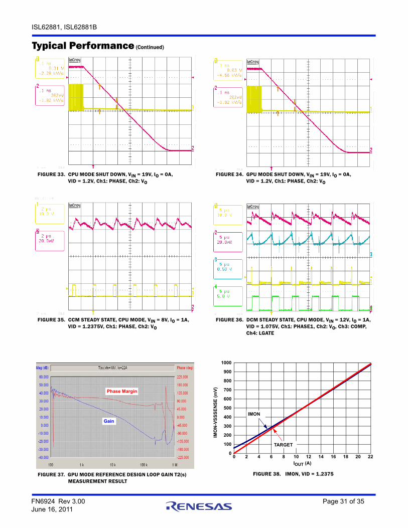
ISL62881, ISL62881B
FIGURE 33. CPU MODE SHUT DOWN, VIN = 19V, IO = 0A, VID = 1.2V, Ch1: PHASE, Ch2: VO
FIGURE 34. GPU MODE SHUT DOWN, VIN = 19V, IO = 0A, VID = 1.2V, Ch1: PHASE, Ch2: VO
FIGURE 35. CCM STEADY STATE, CPU MODE, VIN = 8V, IO = 1A, VID = 1.2375V, Ch1: PHASE, Ch2: VO
FIGURE 36. DCM STEADY STATE, CPU MODE, VIN = 12V, IO = 1A, VID = 1.075V, Ch1: PHASE1, Ch2: VO, Ch3: COMP, Ch4: LGATE
FIGURE 37. GPU MODE REFERENCE DESIGN LOOP GAIN T2(s) MEASUREMENT RESULT
FIGURE 38. IMON, VID = 1.2375
Typical Performance (Continued)
Gain
Phase Margin
0
100
200
300
400
500
600
700
800
900
1000
0 2 4 6 8 10 12 14 16 18 20 22
IOUT (A)
IMO
N-V
SS
SE
NS
E (
mV
)
IMON
TARGET
FN6924 Rev 3.00 Page 31 of 35June 16, 2011
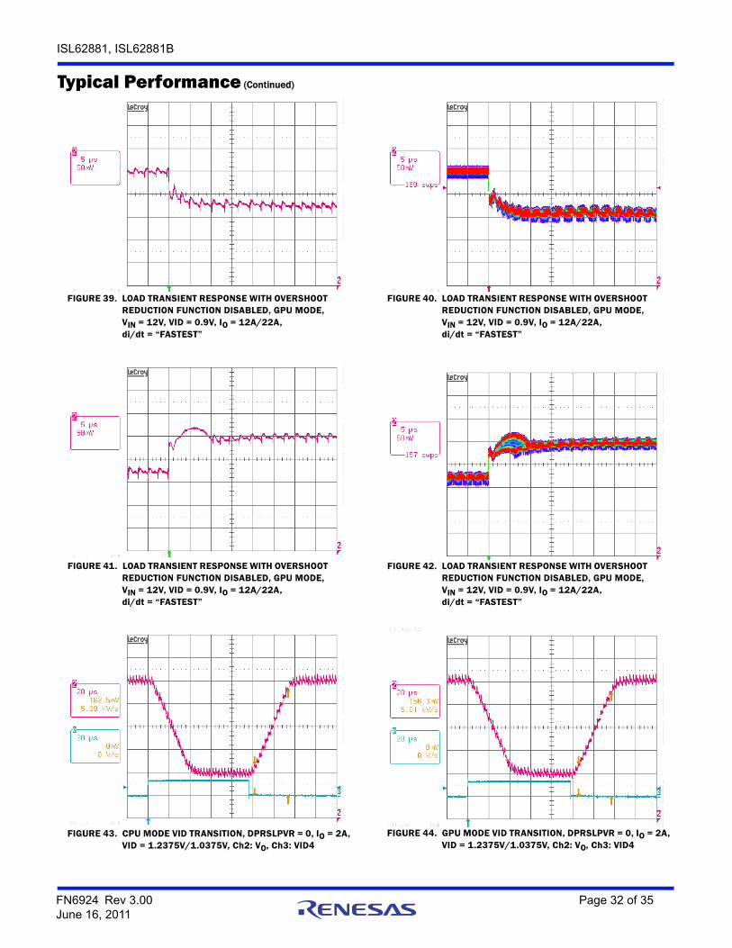
ISL62881, ISL62881B
FIGURE 39. LOAD TRANSIENT RESPONSE WITH OVERSHOOT REDUCTION FUNCTION DISABLED, GPU MODE, VIN = 12V, VID = 0.9V, IO = 12A/22A, di/dt = “FASTEST”
FIGURE 40. LOAD TRANSIENT RESPONSE WITH OVERSHOOT REDUCTION FUNCTION DISABLED, GPU MODE, VIN = 12V, VID = 0.9V, IO = 12A/22A, di/dt = “FASTEST”
FIGURE 41. LOAD TRANSIENT RESPONSE WITH OVERSHOOT REDUCTION FUNCTION DISABLED, GPU MODE, VIN = 12V, VID = 0.9V, IO = 12A/22A, di/dt = “FASTEST”
FIGURE 42. LOAD TRANSIENT RESPONSE WITH OVERSHOOT REDUCTION FUNCTION DISABLED, GPU MODE, VIN = 12V, VID = 0.9V, IO = 12A/22A, di/dt = “FASTEST”
FIGURE 43. CPU MODE VID TRANSITION, DPRSLPVR = 0, IO = 2A, VID = 1.2375V/1.0375V, Ch2: VO, Ch3: VID4
FIGURE 44. GPU MODE VID TRANSITION, DPRSLPVR = 0, IO = 2A, VID = 1.2375V/1.0375V, Ch2: VO, Ch3: VID4
Typical Performance (Continued)
FN6924 Rev 3.00 Page 32 of 35June 16, 2011
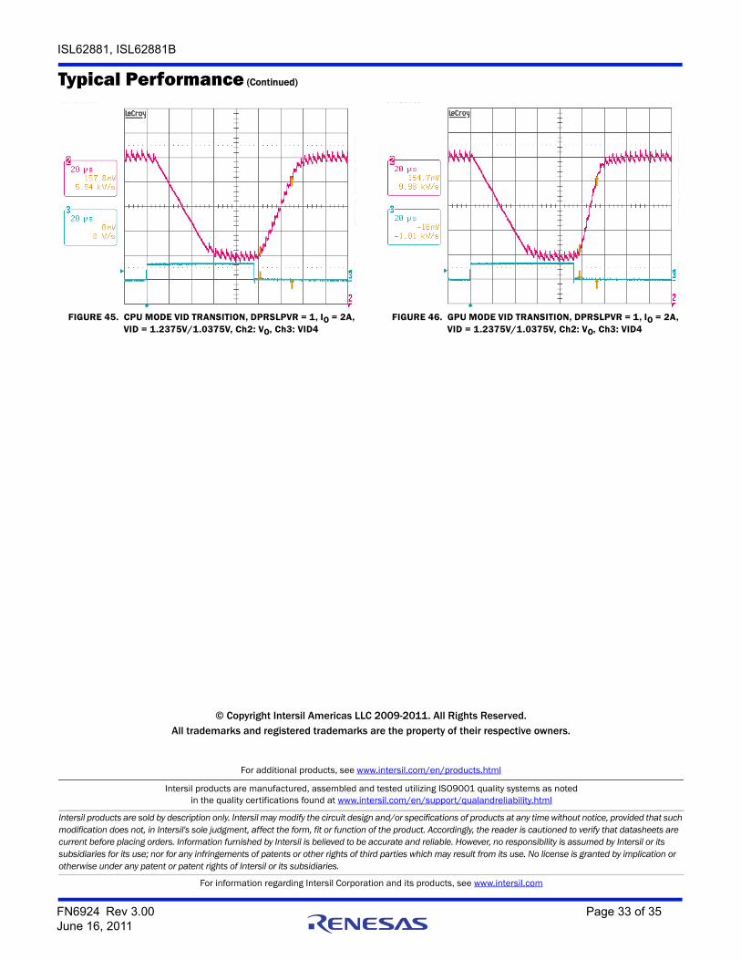
ISL62881, ISL62881B
Intersil products are manufactured, assembled and tested utilizing ISO9001 quality systems as notedin the quality certifications found at www.intersil.com/en/support/qualandreliability.html
Intersil products are sold by description only. Intersil may modify the circuit design and/or specifications of products at any time without notice, provided that such modification does not, in Intersil's sole judgment, affect the form, fit or function of the product. Accordingly, the reader is cautioned to verify that datasheets are current before placing orders. Information furnished by Intersil is believed to be accurate and reliable. However, no responsibility is assumed by Intersil or its subsidiaries for its use; nor for any infringements of patents or other rights of third parties which may result from its use. No license is granted by implication or otherwise under any patent or patent rights of Intersil or its subsidiaries.
For information regarding Intersil Corporation and its products, see www.intersil.com
For additional products, see www.intersil.com/en/products.html
© Copyright Intersil Americas LLC 2009-2011. All Rights Reserved.All trademarks and registered trademarks are the property of their respective owners.
FIGURE 45. CPU MODE VID TRANSITION, DPRSLPVR = 1, IO = 2A, VID = 1.2375V/1.0375V, Ch2: VO, Ch3: VID4
FIGURE 46. GPU MODE VID TRANSITION, DPRSLPVR = 1, IO = 2A, VID = 1.2375V/1.0375V, Ch2: VO, Ch3: VID4
Typical Performance (Continued)
FN6924 Rev 3.00 Page 33 of 35June 16, 2011
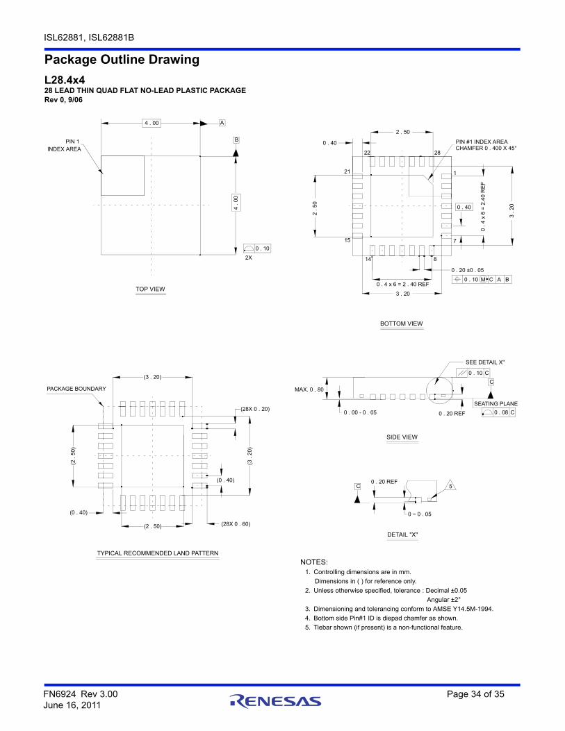
ISL62881, ISL62881B
FN6924 Rev 3.00 Page 34 of 35June 16, 2011
Package Outline Drawing
L28.4x428 LEAD THIN QUAD FLAT NO-LEAD PLASTIC PACKAGERev 0, 9/06
TYPICAL RECOMMENDED LAND PATTERN
DETAIL "X"
TOP VIEW
BOTTOM VIEW
NOTES:1. Controlling dimensions are in mm.
Dimensions in ( ) for reference only.
2. Unless otherwise specified, tolerance : Decimal ±0.05
Angular ±2°
3. Dimensioning and tolerancing conform to AMSE Y14.5M-1994.
4. Bottom side Pin#1 ID is diepad chamfer as shown.
5. Tiebar shown (if present) is a non-functional feature.
PIN 1 INDEX AREA
4 .
00
0 ~ 0 . 05
5
0 . 10
PIN #1 INDEX AREACHAMFER 0 . 400 X 45°
2 . 50
2 .
50
3 .
20
A
PACKAGE BOUNDARY
4 . 00
0 . 40
0 . 20 ±0 . 05
0 . 40
0 . 20 REF0 . 00 - 0 . 05
SEE DETAIL X''
SEATING PLANE
(28X 0 . 60)
(0 . 40)
(28X 0 . 20)
(2 . 50)
(2 .
50
)
(3 . 20)
(3 .
20
)
0 .
4 x
6 =
2.4
0 R
EF
3 . 20
0 . 4 x 6 = 2 . 40 REF
MAX. 0 . 80
(0 . 40)
B
SIDE VIEW
C
C0 . 20 REF
0 . 08 C
0 . 10 C
0 . 10 M C A B
2X 14 8
7
1
2822
21
15
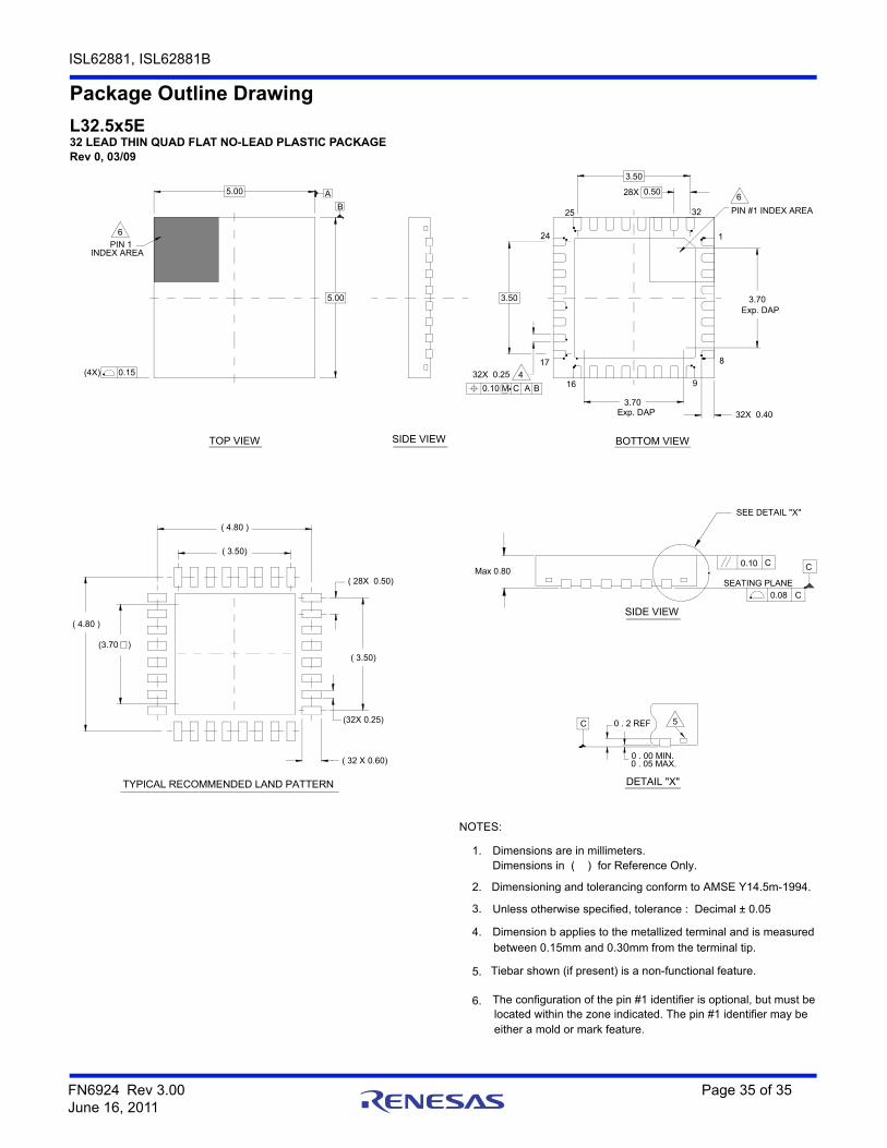
ISL62881, ISL62881B
FN6924 Rev 3.00 Page 35 of 35June 16, 2011
Package Outline Drawing
L32.5x5E32 LEAD THIN QUAD FLAT NO-LEAD PLASTIC PACKAGERev 0, 03/09
located within the zone indicated. The pin #1 identifier may be
Unless otherwise specified, tolerance : Decimal ± 0.05
Tiebar shown (if present) is a non-functional feature.
The configuration of the pin #1 identifier is optional, but must be
between 0.15mm and 0.30mm from the terminal tip.Dimension b applies to the metallized terminal and is measured
Dimensions in ( ) for Reference Only.
Dimensioning and tolerancing conform to AMSE Y14.5m-1994.
6.
either a mold or mark feature.
3.
5.
4.
2.
Dimensions are in millimeters.1.
NOTES:
BOTTOM VIEW
DETAIL "X"
SIDE VIEW
TYPICAL RECOMMENDED LAND PATTERN
TOP VIEW
( 4.80 )
(3.70 )
( 32 X 0.60)
(32X 0.25)
( 28X 0.50)
( 4.80 )
( 3.50)
( 3.50)
C 0 . 2 REF
0 . 05 MAX.0 . 00 MIN.
5
25 PIN #1 INDEX AREA32
3.50
28X 0.50
Exp. DAP
8
124
16
32X 0.40
9
6
3.50
3.70
0.10
32X 0.25
AM C B
4
3.70
Exp. DAP
17
5.00 A
B
5.00
(4X) 0.15
6
PIN 1INDEX AREA
Max 0.80
SEE DETAIL "X"
SEATING PLANE0.08
0.10 CC
C
SIDE VIEW