Embed Size (px)
Citation preview
TUSB544USB/DP/
Custom
Source
AUXp
AUXn
UTX1
UTX2
URX1
URX2
TUSB544
SBU1
SBU2
DTX1
DTX2
DRX1
DRX2
USB PD
Controller
CC1
CC2Control
HPDCTLFLIP 0 1
D+/-
Ty
pe
-C R
ece
pta
cle
Product
Folder
Order
Now
Technical
Documents
Tools &
Software
Support &Community
An IMPORTANT NOTICE at the end of this data sheet addresses availability, warranty, changes, use in safety-critical applications,intellectual property matters and other important disclaimers. PRODUCTION DATA.
TUSB544SLLSEZ0E –APRIL 2017–REVISED APRIL 2018
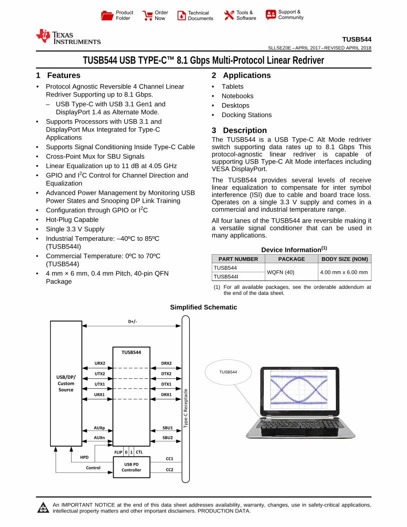
TUSB544 USB TYPE-C™ 8.1 Gbps Multi-Protocol Linear Redriver
1
1 Features1• Protocol Agnostic Reversible 4 Channel Linear
Redriver Supporting up to 8.1 Gbps.– USB Type-C with USB 3.1 Gen1 and
DisplayPort 1.4 as Alternate Mode.• Supports Processors with USB 3.1 and
DisplayPort Mux Integrated for Type-CApplications
• Supports Signal Conditioning Inside Type-C Cable• Cross-Point Mux for SBU Signals• Linear Equalization up to 11 dB at 4.05 GHz• GPIO and I2C Control for Channel Direction and
Equalization• Advanced Power Management by Monitoring USB
Power States and Snooping DP Link Training• Configuration through GPIO or I2C• Hot-Plug Capable• Single 3.3 V Supply• Industrial Temperature: –40ºC to 85ºC
(TUSB544I)• Commercial Temperature: 0ºC to 70ºC
(TUSB544)• 4 mm × 6 mm, 0.4 mm Pitch, 40-pin QFN
Package
2 Applications• Tablets• Notebooks• Desktops• Docking Stations
3 DescriptionThe TUSB544 is a USB Type-C Alt Mode redriverswitch supporting data rates up to 8.1 Gbps Thisprotocol-agnostic linear redriver is capable ofsupporting USB Type-C Alt Mode interfaces includingVESA DisplayPort.
The TUSB544 provides several levels of receivelinear equalization to compensate for inter symbolinterference (ISI) due to cable and board trace loss.Operates on a single 3.3 V supply and comes in acommercial and industrial temperature range.
All four lanes of the TUSB544 are reversible making ita versatile signal conditioner that can be used inmany applications.
Device Information(1)
PART NUMBER PACKAGE BODY SIZE (NOM)TUSB544
WQFN (40) 4.00 mm x 6.00 mmTUSB544I
(1) For all available packages, see the orderable addendum atthe end of the data sheet.
Simplified Schematic
2
TUSB544SLLSEZ0E –APRIL 2017–REVISED APRIL 2018 www.ti.com
Product Folder Links: TUSB544
Submit Documentation Feedback Copyright © 2017–2018, Texas Instruments Incorporated
Table of Contents1 Features .................................................................. 12 Applications ........................................................... 13 Description ............................................................. 14 Revision History..................................................... 25 Pin Configuration and Functions ......................... 46 Specifications......................................................... 6
6.1 Absolute Maximum Ratings ...................................... 66.2 ESD Ratings.............................................................. 66.3 Recommended Operating Conditions....................... 66.4 Thermal Information .................................................. 76.5 Power Supply Characteristics ................................... 76.6 DC Electrical Characteristics .................................... 76.7 AC Electrical Characteristics..................................... 86.8 Timing Requirements .............................................. 106.9 Switching Characteristics ........................................ 106.10 Typical Characteristics .......................................... 13
7 Detailed Description ............................................ 167.1 Overview ................................................................. 167.2 Functional Block Diagram ....................................... 177.3 Feature Description................................................. 18
7.4 Device Functional Modes........................................ 197.5 Programming .......................................................... 337.6 Register Maps ........................................................ 34
8 Application and Implementation ........................ 438.1 Application Information............................................ 438.2 Typical Application ................................................. 438.3 System Examples .................................................. 47
9 Power Supply Recommendations ...................... 5410 Layout................................................................... 55
10.1 Layout Guidelines ................................................. 5510.2 Layout Example .................................................... 55
11 Device and Documentation Support ................. 5611.1 Documentation Support ....................................... 5611.2 Receiving Notification of Documentation Updates 5611.3 Community Resources.......................................... 5611.4 Trademarks ........................................................... 5611.5 Electrostatic Discharge Caution............................ 5611.6 Glossary ................................................................ 56
12 Mechanical, Packaging, and OrderableInformation ........................................................... 56
4 Revision HistoryNOTE: Page numbers for previous revisions may differ from page numbers in the current version.
Changes from Revision D (November 2017) to Revision E Page
• Changed the Simplified Schematic......................................................................................................................................... 1
Changes from Revision C (October 2017) to Revision D Page
• Changed text of the second paragraph in the DESCRIPTION From: "..cable and board trace loss due to intersymbol interference (ISI)" To: "..inter symbol interference (ISI) due to cable and board trace loss." ................................... 1
• Changed Pin 2 and Pin 35 text From: "When I2C_EN !=0,.." To: "In I2C mode,.." in the Pin Functions............................... 4• Changed Pin 14 text From: "..levels for the GPIO configuration.." To: "..levels for the 2-level GPIO configuration.." in
the Pin Functions .................................................................................................................................................................... 5• Changed Pin 17 in the text From: 0 = GPIO Mode (I2C disabled) To: 0 = GPIO Mode AUX Snoop enabled (I2C
disabled) in the Pin Functions ................................................................................................................................................ 5• Changed Pins 21, 22, and 23 From: "When I2C_EN !=0,.." To: "In GPIO mode,.." in the Pin Functions.............................. 5• Removed "When I2C_EN = 0" from pin 32. .......................................................................................................................... 5• In pin 32, changed 2ms to tCTL1_DEBOUNCE ............................................................................................................................... 5• From: DEQ1 sets the high-frequency equalizer gain for downstream facing URX1, URX2, UTX1, UTX2 receivers.
To: DEQ1 sets the high-frequency equalizer gain for downstream facing DRX1, DRX2, DTX1, DTX2 receivers ............... 5• Deleted the MAX value of 10 ms from tCTL1_DEBOUNCE in the Switching Characteristics ....................................................... 10• Added test Condition " DP lanes will be disabled if low for greater than min value" for tCTL1_DEBOUNCE in the Switching
Characteristics ...................................................................................................................................................................... 10• Changed text From: "There is an internal 30 kΩ pull-up and a 94kΩ pull-down." To: "There are internal pull-up and a
pull-down resisters." in 4-Level Inputs .................................................................................................................................. 18• Changed text From: "..when I2C_EN = “0”." To: "..when I2C_EN = “0” or "F"." in the first paragraph of Device
Configuration in GPIO Mode ................................................................................................................................................ 19• Changed Table 4 .................................................................................................................................................................. 21• Changed text From: "..when I2C_EN is not equal to “0”." To: "..when I2C_EN is equal to “1”. " in Device
3
TUSB544www.ti.com SLLSEZ0E –APRIL 2017–REVISED APRIL 2018
Product Folder Links: TUSB544
Submit Documentation FeedbackCopyright © 2017–2018, Texas Instruments Incorporated
Configuration in I2C Mode.................................................................................................................................................... 28• Changed text From: "When I2C_EN is ‘0’,.." To: :In I2C mode,.." in DisplayPort Mode ...................................................... 29• Changed text From: "When I2C_EN is ‘0’,.." To: :In GPIO mode,.." in Custom Alternate Mode ......................................... 29• Deleted the Cable Mode section and all "cable mode" from datasheet. ............................................................................. 29• Changed Table 12 ................................................................................................................................................................ 35• Changed Bit 5-2 Type From: R/WU To: R/W in Table 15 .................................................................................................... 36• Changed Bit 7-0 Type From: R/WU To: R/W in Figure 25 and Table 16............................................................................. 37• Changed Bit 7-0 Type From: R/WU To: R/W in Figure 26 and Table 17............................................................................. 37• Changed Bit 6-0 Type From: RU To: RH in Figure 27 and Table 18................................................................................... 38• Changed Figure 29 and Table 20......................................................................................................................................... 40• Changed Bit 7-0 Type From: R/WU To: R/W in Figure 30 and Table 21............................................................................. 40• Changed Bit 3-0 Type From: R/WU To: R/W in Figure 31 and Table 22............................................................................. 41• Changed bit 7 From: R/WU To: RH in Figure 32 and Table 23 ........................................................................................... 41• USB3.1_# register default changed to 4h from 0h. .............................................................................................................. 41• Changed USB3.1_4 register default to 23h from 00h. ........................................................................................................ 42• Changed SBU1, and SBU2 pin labels on the Sink side of Figure 40................................................................................... 48• Changed SBU1, and SBU2 pin labels on the Sink side of Figure 41................................................................................... 49• Changed SBU1, and SBU2 pin labels on the Sink side of Figure 42................................................................................... 49• Changed SBU1, and SBU2 pin labels on the Sink side of Figure 48................................................................................... 52• Changed SBU1, and SBU2 pin labels on the Sink side of Figure 49................................................................................... 53• Changed SBU1, and SBU2 pin labels on the Sink side of Figure 50................................................................................... 53
Changes from Revision B (Mayl 2017) to Revision C Page
• Changed Tcfg_su From: 350 ms To: 350 µs in Table 9 .......................................................................................................... 33
Changes from Revision A (April 2017) to Revision B Page
• Added a MIN value of 0.5 pF to CI_I2C in the DC Electrical Characteristics table .................................................................. 8• Changed VRX-DC-CM, deleted the MIN and MAX values and added TYP = 0 V in the AC Electrical Characteristics table...... 8• Changed EQSS Description From: "Receiver equalization" To: "Receiver equalization at maximum setting" in the AC
Electrical Characteristics table ............................................................................................................................................... 8• Changed EQSS From: MAX = 9.8 dB To: MAX = 9 dB in the AC Electrical Characteristics table ......................................... 8• Changed VTX-DC-CM, deleted the MIN and MAX values and added TYP = 1.75 V in the AC Electrical Characteristics table. 8• Changed RLTX-DIFF From: TYP = -14 dB To: TYP = -13 dB in the AC Electrical Characteristics table................................... 9• Changed RLTX-CM From: TYP = -13 dB To: TYP = -11 dB in the AC Electrical Characteristics table .................................... 9• Changed GLF From: MAX = 2.5 dB To: MAX = 1 dB in the AC Electrical Characteristics table ............................................ 9• Changed VIC, deleted the MIN and MAX values and added TYP = 0 V in the AC Electrical Characteristics table............... 9• Changed the EQDP entry in the AC Electrical Characteristics table ....................................................................................... 9• Changed VTX(DC-CM), deleted the MIN and MAX values and added TYP = 1.75 V in the AC Electrical Characteristics table 9• Changed the tIDLEExit_DISC value From: TYP = 10 µs To TYP = 15 ms in the Timing Requirements table............................ 10• Changed the tCTL1_DEBOUNCE value From: MIN = 2 ms To: MIN = 3 ms in the Switching Characteristics table ................... 10
Changes from Original (April 2017) to Revision A Page
• Changed SBU1, SBU2, AUXn, and AUXp pin labels on the Sink side of Figure 45............................................................ 51• Changed SBU1, SBU2, AUXn, and AUXp pin labels on the Sink side of Figure 46............................................................ 51
Thermal
Pad
1VCC
2UEQ1/A1
3CFG0
4CFG1
5SWAP
6VCC
7SLP_S0#
8DIR0
9U
RX
2p
10U
RX
2n
11D
IR1
12U
TX
2p
13U
TX
2n
14V
IO_S
EL
15U
TX
1n
16U
TX
1p
17I2
C_E
N
18U
RX
1n
19U
RX
1p
20V
CC
21 FLIP/SCL
22 CTL0/SDA
23 CTL1
24 AUXp
25 AUXn
26 SBU2
27 SBU1
28 VCC
29D
EQ
1
30D
RX
1p
31D
RX
1n
32H
PD
IN
33D
TX
1p
34D
TX
1n
35U
EQ
0/A
0
36D
TX
2n
37D
TX
2p
38D
EQ
0
39D
RX
2n
40D
RX
2p
Not to scale
4
TUSB544SLLSEZ0E –APRIL 2017–REVISED APRIL 2018 www.ti.com
Product Folder Links: TUSB544
Submit Documentation Feedback Copyright © 2017–2018, Texas Instruments Incorporated
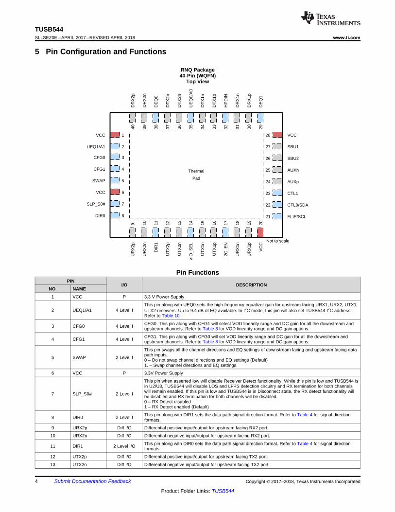
5 Pin Configuration and Functions
RNQ Package40-Pin (WQFN)
Top View
Pin FunctionsPIN
I/O DESCRIPTIONNO. NAME
1 VCC P 3.3 V Power Supply
2 UEQ1/A1 4 Level IThis pin along with UEQ0 sets the high-frequency equalizer gain for upstream facing URX1, URX2, UTX1,UTX2 receivers. Up to 9.4 dB of EQ available. In I2C mode, this pin will also set TUSB544 I2C address.Refer to Table 10.
3 CFG0 4 Level I CFG0. This pin along with CFG1 will select VOD linearity range and DC gain for all the downstream andupstream channels. Refer to Table 8 for VOD linearity range and DC gain options.
4 CFG1 4 Level I CFG1. This pin along with CFG0 will set VOD linearity range and DC gain for all the downstream andupstream channels. Refer to Table 8 for VOD linearity range and DC gain options.
5 SWAP 2 Level I
This pin swaps all the channel directions and EQ settings of downstream facing and upstream facing datapath inputs.0 – Do not swap channel directions and EQ settings (Default)1. – Swap channel directions and EQ settings.
6 VCC P 3.3V Power Supply
7 SLP_S0# 2 Level I
This pin when asserted low will disable Receiver Detect functionality. While this pin is low and TUSB544 isin U2/U3, TUSB544 will disable LOS and LFPS detection circuitry and RX termination for both channelswill remain enabled. If this pin is low and TUSB544 is in Disconnect state, the RX detect functionality willbe disabled and RX termination for both channels will be disabled.0 – RX Detect disabled1 – RX Detect enabled (Default)
8 DIR0 2 Level I This pin along with DIR1 sets the data path signal direction format. Refer to Table 4 for signal directionformats.
9 URX2p Diff I/O Differential positive input/output for upstream facing RX2 port.
10 URX2n Diff I/O Differential negative input/output for upstream facing RX2 port.
11 DIR1 2 Level I/O This pin along with DIR0 sets the data path signal direction format. Refer to Table 4 for signal directionformats.
12 UTX2p Diff I/O Differential positive input/output for upstream facing TX2 port.
13 UTX2n Diff I/O Differential negative input/output for upstream facing TX2 port.
5
TUSB544www.ti.com SLLSEZ0E –APRIL 2017–REVISED APRIL 2018
Product Folder Links: TUSB544
Submit Documentation FeedbackCopyright © 2017–2018, Texas Instruments Incorporated
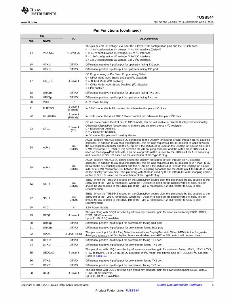
Pin Functions (continued)PIN
I/O DESCRIPTIONNO. NAME
14 VIO_SEL 4 Level I/O
This pin selects I/O voltage levels for the 2-level GPIO configuration pins and the I2C interface:0 = 3.3-V configuration I/O voltage, 3.3-V I2C interface (Default)R = 3.3-V configuration I/O voltage, 1.8-V I2C interfaceF = 1.8-V configuration I/O voltage, 3.3-V I2C interface1 = 1.8-V configuration I/O voltage, 1.8-V I2C interface.
15 UTX1n Diff I/O Differential negative input/output for upstream facing TX1 port.
16 UTX1p Diff I/O Differential positive input/output for upstream facing TX1 port.
17 I2C_EN 4 Level I
I2C Programming or Pin Strap Programming Select.0 = GPIO Mode AUX Snoop enabled (I2C disabled)R = TI Test Mode (I2C enabled)F = GPIO Mode, AUX Snoop Disabled (I2C disabled)1 = I2C enabled.
18 URX1n Diff I/O Differential negative input/output for upstream facing RX1 port.
19 URX1p Diff I/O Differential positive input/output for upstream facing RX1 port.
20 VCC P 3.3V Power Supply
21 FLIP/SCL 2 Level I(Failsafe) In GPIO mode, this is Flip control pin, otherwise this pin is I2C clock.
22 CTL0/SDA 2 Level I(Failsafe) In GPIO mode, this is a USB3.1 Switch control pin, otherwise this pin is I2C data.
23 CTL1 2 Level I(PD)
DP Alt mode Switch Control Pin. In GPIO mode, this pin will enable or disable DisplayPort functionality.Otherwise DisplayPort functionality is enabled and disabled through I2C registers.L = DisplayPort Disabled.H = DisplayPort Enabled.In I2C mode, this pin is not used by device.
24 AUXp I/O,CMOS
AUXp. DisplayPort AUX positive I/O connected to the DisplayPort source or sink through an AC couplingcapacitor. In addition to AC coupling capacitor, this pin also requires a 100-kΩ resistor to GND betweenthe AC coupling capacitor and the AUXp pin if the TUSB544 is used on the DisplayPort source side, or a1-MΩ resistor to DP_PWR (3.3V) between the AC coupling capacitor and the AUXp pin if TUSB544 isused on the DisplayPort sink side. This pin along with AUXn is used by the TUSB544 for AUX snoopingand is routed to SBU1/2 based on the orientation of the Type-C plug.
25 AUXn I/O,CMOS
AUXn. DisplayPort AUX I/O connected to the DisplayPort source or sink through an AC couplingcapacitor. In addition to AC coupling capacitor, this pin also requires a 100-kΩ resistor to DP_PWR (3.3V)between the AC coupling capacitor and the AUXn pin if the TUSB544 is used on the DisplayPort sourceside, or a 1-MΩ resistor to GND between the AC coupling capacitor and the AUXn pin if TUSB544 is usedon the DisplayPort sink side. This pin along with AUXp is used by the TUSB544 for AUX snooping and isrouted to SBU1/2 based on the orientation of the Type-C plug.
26 SBU2 I/O,CMOS
SBU2. When the TUSB544 is used on the DisplayPort source side, this pin should be DC coupled to theSBU2 pin of the Type-C receptacle. When the TUSB544 is used on the DisplayPort sink side, this pinshould be DC coupled to the SBU1 pin of the Type-C receptacle. A 2-MΩ resistor to GND is alsorecommended.
27 SBU1 I/O,CMOS
SBU1. When the TUSB544 is used on the DisplayPort source side, this pin should be DC coupled to theSBU1 pin of the Type-C receptacle. When the TUSB544 is used on the DisplayPort sink side, this pinshould be DC coupled to the SBU2 pin of the Type-C receptacle. A 2-MΩ resistor to GND is alsorecommended.
28 VCC P 3.3V Power Supply
29 DEQ1 4 Level IThis pin along with DEQ0 sets the high-frequency equalizer gain for downstream facing DRX1, DRX2,DTX1, DTX2 receivers.Up to 11 dB of EQ available.
30 DRX1p Diff I/O Differential positive input/output for downstream facing RX1 port.
31 DRX1n Diff I/O Differential negative input/output for downstream facing RX1 port.
32 HPDIN 2 Level I (PD) This pin is an input for Hot Plug Detect received from DisplayPort sink. When HPDIN is low for greaterthan tCTL1_DEBOUNCE, all DisplayPort lanes are disabled and AUX to SBU switch will remain closed.
33 DTX1p Diff I/O Differential positive input/output for downstream facing TX1 port.
34 DTX1n Diff I/O Differential negative input/output for downstream facing TX1 port.
35 UEQ0/A0 4 Level IThis pin along with UEQ1 sets the high-frequency equalizer gain for upstream facing URX1, URX2, UTX1,UTX2 receivers. Up to 9.4 dB of EQ available. In I2C mode, this pin will also set TUSB544 I2C address.Refer to Table 10.
36 DTX2n Diff I/O Differential negative input/output for downstream facing TX2 port.
37 DTX2p Diff I/O Differential positive input/output for downstream facing TX2 port.
38 DEQ0 4 Level IThis pin along with DEQ1 sets the high-frequency equalizer gain for downstream facing DRX1, DRX2,DTX1, DTX2 receivers.Up to 11 dB of EQ available.
6
TUSB544SLLSEZ0E –APRIL 2017–REVISED APRIL 2018 www.ti.com
Product Folder Links: TUSB544
Submit Documentation Feedback Copyright © 2017–2018, Texas Instruments Incorporated
Pin Functions (continued)PIN
I/O DESCRIPTIONNO. NAME
39 DRX2n Diff I/O Differential negative input/output for downstream facing RX2 port.
40 DRX2p Diff I/O Differential positive input/output for downstream facing RX2 port.
Thermal Pad GND Ground
(1) Stresses beyond those listed under Absolute Maximum Ratings may cause permanent damage to the device. These are stress ratingsonly, which do not imply functional operation of the device at these or any other conditions beyond those indicated under RecommendedOperating Conditions. Exposure to absolute-maximum-rated conditions for extended periods may affect device reliability.
6 Specifications
6.1 Absolute Maximum Ratingsover operating free-air temperature range (unless otherwise noted) (1)
MIN MAX UNITSupply Voltage VCC –0.3 4 V
Voltage Range at any input or output pin
Differential voltage between positive andnegative inputs –2.5 2.5 V
Voltage at differential inputs –0.5 VCC + 0.5 VCMOS Inputs –0.5 VCC + 0.5 V
Maximum junction temperature, TJ 125 °CStorage temperature ,TSTG –65 150 °C
(1) JEDEC document JEP155 states that 500-V HBM allows safe manufacturing with a standard ESD control process.(2) JEDEC document JEP157 states that 250-V CDM allows safe manufacturing with a standard ESD control process.
6.2 ESD RatingsVALUE UNIT
V(ESD) Electrostatic dischargeHuman-body model (HBM), per ANSI/ESDA/JEDEC JS-001 (1) ±6 kVCharged-device model (CDM), per JEDEC specification JESD22-C101 (2) ±1500 V
6.3 Recommended Operating Conditionsover operating free-air temperature range (unless otherwise noted)
MIN NOM MAX UNIT
VCCMain power supply 3 3.3 3.6 VSupply ramp requirement 100 ms
VI2C Supply that external resistors on SDA and SCL are pulled up to. 1.70 3.6 VVPSN Supply Noise on VCC terminals 100 mV
TA Operating free-air temperatureTUSB544 0 70 °CTUSB544I –40 85 °C
7
TUSB544www.ti.com SLLSEZ0E –APRIL 2017–REVISED APRIL 2018
Product Folder Links: TUSB544
Submit Documentation FeedbackCopyright © 2017–2018, Texas Instruments Incorporated
(1) For more information about traditional and new thermal metrics, see the Semiconductor and IC Package Thermal Metrics applicationreport.
6.4 Thermal Information
THERMAL METRIC (1)TUSB544
UNITRNQ (QFN)40 PINS
RθJA Junction-to-ambient thermal resistance 37.6 °C/WRθJC(top) Junction-to-case (top) thermal resistance 20.7 °C/WRθJB Junction-to-board thermal resistance 9.5 °C/WψJT Junction-to-top characterization parameter 0.2 °C/WψJB Junction-to-board characterization parameter 9.4 °C/WRθJC(bot) Junction-to-case (bottom) thermal resistance 2.3 °C/W
6.5 Power Supply Characteristicsover operating free-air temperature range (unless otherwise noted)
PARAMETER TEST CONDITIONS MIN TYP MAX UNIT
PCC-ACTIVE-USBAverage active powerUSB Only
Link in U0 with GEN1 data transmission.EQ control pins = NC, K28.5 pattern at 5Gbps, VID = 1000 mVp-p ; VOD Linearity =900 mVp-p; CTL1 = L; CTL0 = H
297 mW
PCC-ACTIVE-USB-DP1Average active powerUSB + 2 Lane DP
Link in U0 with GEN1 data transmission.EQ control pins = NC, K28.5 pattern at 5Gbps, VID = 1000 mVp-p; VOD Linearity =900 mVp-p; CTL1 = H; CTL0 = H
578 mW
PCC-ACTIVE-USB-CUSTOM
Average active powerUSB + 2 ChannelCustom Alt Mode
Link in U0 with GEN1 data transmission.EQ control pins = NC, K28.5 pattern at 5Gbps, VID = 1000 mVp-p; VOD Linearity =900 mVp-p; CTL1 = H; CTL0 = H
578 mW
PCC-Active-DPAverage active power4 Lane DP Only
Four active DP lanes operating at 8.1Gbps; EQ control pins = NC, K28.5 patternat 5 Gbps, VID = 1000 mVp-p; VODLinearity = 900 mVp-p; CTL1 = H; CTL0 =L;
564 mW
PCC-NC-USB Average power with no connection No GEN1 device is connected toTXP/TXN; CTL1 = L; CTL0 = H; 2.5 mW
PCC-U2U3 Average power in U2/U3 Link in U2 or U3 USB Mode Only; CTL1 =L; CTL0 = H; 2.0 mW
PCC-SHUTDOWN Device Shutdown CTL1 = L; CTL0 = L; I2C_EN = 0; 0.65 mW
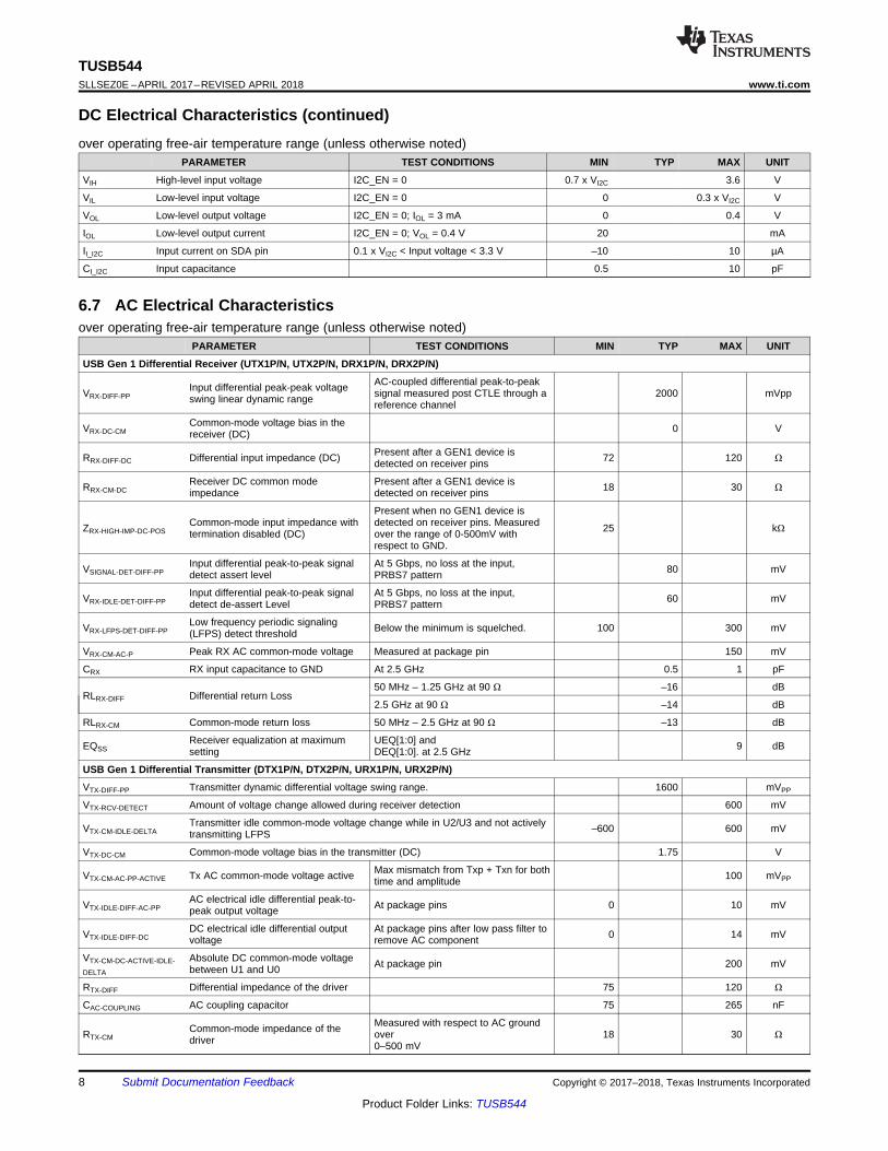
6.6 DC Electrical Characteristicsover operating free-air temperature range (unless otherwise noted)
PARAMETER TEST CONDITIONS MIN TYP MAX UNIT
4-State CMOS Inputs(UEQ[1:0];DEQ[1:0], CFG[1:0], A[1:0], I2C_EN, VIO_SEL)
IIH High level input current VCC = 3.6 VIN = 3.6 V 20 80 µA
IIL Low level input current VCC = 3.6 V; VIN = 0 V –160 –40 µA
4-Level VTH
Threshold 0 / R VCC = 3.3 V 0.55 V
Threshold R/ Float VCC = 3.3 V 1.65 V
Threshold Float / 1 VCC = 3.3 V 2.7 V
RPU Internal pull-up resistance 35 kΩ
RPD Internal pull-down resistance 95 kΩ
2-State CMOS Input (CTL0, CTL1, FLIP, HPDIN, SLP_S0#, SWAP, DIR[1:0]).
VIH High-level input voltage 0.7×VIO 3.6 V
VIL Low-level input voltage 0 0.3×VIO V
RPD Internal pull-down resistance for CTL1 500 kΩ
IIH High-level input current VIN = 3.6 V –25 25 µA
IIL Low-level input current VIN = GND, VCC = 3.6 V –25 25 µA
I2C Control Pins SCL, SDA
8
TUSB544SLLSEZ0E –APRIL 2017–REVISED APRIL 2018 www.ti.com
Product Folder Links: TUSB544
Submit Documentation Feedback Copyright © 2017–2018, Texas Instruments Incorporated
DC Electrical Characteristics (continued)over operating free-air temperature range (unless otherwise noted)
PARAMETER TEST CONDITIONS MIN TYP MAX UNIT
VIH High-level input voltage I2C_EN = 0 0.7 x VI2C 3.6 V
VIL Low-level input voltage I2C_EN = 0 0 0.3 x VI2C V
VOL Low-level output voltage I2C_EN = 0; IOL = 3 mA 0 0.4 V
IOL Low-level output current I2C_EN = 0; VOL = 0.4 V 20 mA
II_I2C Input current on SDA pin 0.1 x VI2C < Input voltage < 3.3 V –10 10 µA
CI_I2C Input capacitance 0.5 10 pF
6.7 AC Electrical Characteristicsover operating free-air temperature range (unless otherwise noted)
PARAMETER TEST CONDITIONS MIN TYP MAX UNIT
USB Gen 1 Differential Receiver (UTX1P/N, UTX2P/N, DRX1P/N, DRX2P/N)
VRX-DIFF-PPInput differential peak-peak voltageswing linear dynamic range
AC-coupled differential peak-to-peaksignal measured post CTLE through areference channel
2000 mVpp
VRX-DC-CMCommon-mode voltage bias in thereceiver (DC) 0 V
RRX-DIFF-DC Differential input impedance (DC) Present after a GEN1 device isdetected on receiver pins 72 120 Ω
RRX-CM-DCReceiver DC common modeimpedance
Present after a GEN1 device isdetected on receiver pins 18 30 Ω
ZRX-HIGH-IMP-DC-POSCommon-mode input impedance withtermination disabled (DC)
Present when no GEN1 device isdetected on receiver pins. Measuredover the range of 0-500mV withrespect to GND.
25 kΩ
VSIGNAL-DET-DIFF-PPInput differential peak-to-peak signaldetect assert level
At 5 Gbps, no loss at the input,PRBS7 pattern 80 mV
VRX-IDLE-DET-DIFF-PPInput differential peak-to-peak signaldetect de-assert Level
At 5 Gbps, no loss at the input,PRBS7 pattern 60 mV
VRX-LFPS-DET-DIFF-PPLow frequency periodic signaling(LFPS) detect threshold Below the minimum is squelched. 100 300 mV
VRX-CM-AC-P Peak RX AC common-mode voltage Measured at package pin 150 mV
CRX RX input capacitance to GND At 2.5 GHz 0.5 1 pF
RLRX-DIFF Differential return Loss50 MHz – 1.25 GHz at 90 Ω –16 dB
2.5 GHz at 90 Ω –14 dB
RLRX-CM Common-mode return loss 50 MHz – 2.5 GHz at 90 Ω –13 dB
EQSSReceiver equalization at maximumsetting
UEQ[1:0] andDEQ[1:0]. at 2.5 GHz 9 dB
USB Gen 1 Differential Transmitter (DTX1P/N, DTX2P/N, URX1P/N, URX2P/N)
VTX-DIFF-PP Transmitter dynamic differential voltage swing range. 1600 mVPP
VTX-RCV-DETECT Amount of voltage change allowed during receiver detection 600 mV
VTX-CM-IDLE-DELTATransmitter idle common-mode voltage change while in U2/U3 and not activelytransmitting LFPS –600 600 mV
VTX-DC-CM Common-mode voltage bias in the transmitter (DC) 1.75 V
VTX-CM-AC-PP-ACTIVE Tx AC common-mode voltage active Max mismatch from Txp + Txn for bothtime and amplitude 100 mVPP
VTX-IDLE-DIFF-AC-PPAC electrical idle differential peak-to-peak output voltage At package pins 0 10 mV
VTX-IDLE-DIFF-DCDC electrical idle differential outputvoltage
At package pins after low pass filter toremove AC component 0 14 mV
VTX-CM-DC-ACTIVE-IDLE-DELTA
Absolute DC common-mode voltagebetween U1 and U0 At package pin 200 mV
RTX-DIFF Differential impedance of the driver 75 120 Ω
CAC-COUPLING AC coupling capacitor 75 265 nF
RTX-CMCommon-mode impedance of thedriver
Measured with respect to AC groundover0–500 mV
18 30 Ω
9
TUSB544www.ti.com SLLSEZ0E –APRIL 2017–REVISED APRIL 2018
Product Folder Links: TUSB544
Submit Documentation FeedbackCopyright © 2017–2018, Texas Instruments Incorporated
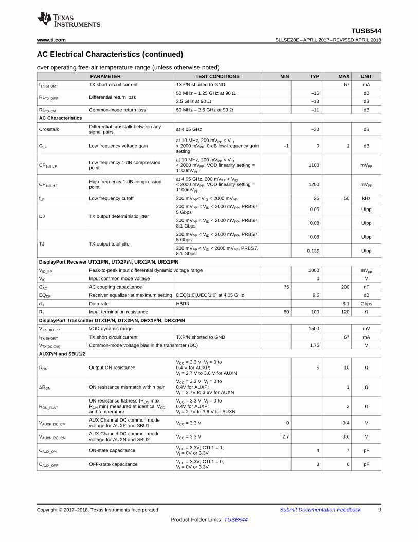
AC Electrical Characteristics (continued)over operating free-air temperature range (unless otherwise noted)
PARAMETER TEST CONDITIONS MIN TYP MAX UNIT
ITX-SHORT TX short circuit current TXP/N shorted to GND 67 mA
RLTX-DIFF Differential return loss50 MHz – 1.25 GHz at 90 Ω –16 dB
2.5 GHz at 90 Ω –13 dB
RLTX-CM Common-mode return loss 50 MHz – 2.5 GHz at 90 Ω –11 dB
AC Characteristics
Crosstalk Differential crosstalk between anysignal pairs at 4.05 GHz –30 dB
GLF Low frequency voltage gainat 10 MHz, 200 mVPP < VID< 2000 mVPP; 0-dB low-frequency gainsetting
–1 0 1 dB
CP1dB-LFLow frequency 1-dB compressionpoint
at 10 MHz, 200 mVPP < VID< 2000 mVPP; VOD linearity setting =1100mVPP
1100 mVPP
CP1dB-HFHigh frequency 1-dB compressionpoint
at 4.05 GHz, 200 mVPP < VID< 2000 mVPP; VOD linearity setting =1100mVPP
1200 mVPP
fLF Low frequency cutoff 200 mVPP< VID < 2000 mVPP 25 50 kHz
DJ TX output deterministic jitter
200 mVPP < VID < 2000 mVPP, PRBS7,5 Gbps 0.05 UIpp
200 mVPP < VID < 2000 mVPP, PRBS7,8.1 Gbps 0.08 UIpp
TJ TX output total jitter
200 mVPP < VID < 2000 mVPP, PRBS7,5 Gbps 0.08 UIpp
200 mVPP < VID < 2000 mVPP, PRBS7,8.1 Gbps 0.135 UIpp
DisplayPort Receiver UTX1P/N, UTX2P/N, URX1P/N, URX2P/N
VID_PP Peak-to-peak input differential dynamic voltage range 2000 mVpp
VIC Input common mode voltage 0 V
CAC AC coupling capacitance 75 200 nF
EQDP Receiver equalizer at maximum setting DEQ[1:0],UEQ[1:0] at 4.05 GHz 9.5 dB
dR Data rate HBR3 8.1 Gbps
Rti Input termination resistance 80 100 120 Ω
DisplayPort Transmitter DTX1P/N, DTX2P/N, DRX1P/N, DRX2P/N
VTX-DIFFPP VOD dynamic range 1500 mV
ITX-SHORT TX short circuit current TXP/N shorted to GND 67 mA
VTX(DC-CM) Common-mode voltage bias in the transmitter (DC) 1.75 V
AUXP/N and SBU1/2
RON Output ON resistanceVCC = 3.3 V; VI = 0 to0.4 V for AUXP;VI = 2.7 V to 3.6 V for AUXN
5 10 Ω
ΔRON ON resistance mismatch within pairVCC = 3.3 V; VI = 0 to0.4V for AUXP;VI = 2.7V to 3.6V for AUXN
1 Ω
RON_FLAT
ON resistance flatness (RON max –RON min) measured at identical VCCand temperature
VCC = 3.3 V; VI = 0 to0.4V for AUXP;VI = 2.7V to 3.6 V for AUXN
2 Ω
VAUXP_DC_CMAUX Channel DC common modevoltage for AUXP and SBU1. VCC = 3.3 V 0 0.4 V
VAUXN_DC_CMAUX Channel DC common modevoltage for AUXN and SBU2 VCC = 3.3 V 2.7 3.6 V
CAUX_ON ON-state capacitance VCC = 3.3V; CTL1 = 1;VI = 0V or 3.3V 4 7 pF
CAUX_OFF OFF-state capacitance VCC = 3.3V; CTL1 = 0;VI = 0V or 3.3V 3 6 pF
10
TUSB544SLLSEZ0E –APRIL 2017–REVISED APRIL 2018 www.ti.com
Product Folder Links: TUSB544
Submit Documentation Feedback Copyright © 2017–2018, Texas Instruments Incorporated
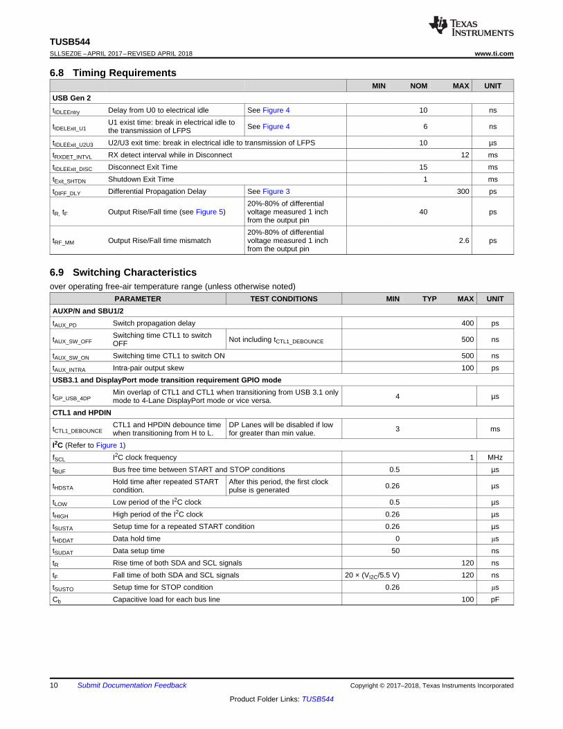
6.8 Timing RequirementsMIN NOM MAX UNIT
USB Gen 2tIDLEEntry Delay from U0 to electrical idle See Figure 4 10 ns
tIDELExit_U1U1 exist time: break in electrical idle tothe transmission of LFPS See Figure 4 6 ns
tIDLEExit_U2U3 U2/U3 exit time: break in electrical idle to transmission of LFPS 10 µstRXDET_INTVL RX detect interval while in Disconnect 12 mstIDLEExit_DISC Disconnect Exit Time 15 mstExit_SHTDN Shutdown Exit Time 1 mstDIFF_DLY Differential Propagation Delay See Figure 3 300 ps
tR, tF Output Rise/Fall time (see Figure 5)20%-80% of differentialvoltage measured 1 inchfrom the output pin
40 ps
tRF_MM Output Rise/Fall time mismatch20%-80% of differentialvoltage measured 1 inchfrom the output pin
2.6 ps
6.9 Switching Characteristicsover operating free-air temperature range (unless otherwise noted)
PARAMETER TEST CONDITIONS MIN TYP MAX UNITAUXP/N and SBU1/2tAUX_PD Switch propagation delay 400 ps
tAUX_SW_OFFSwitching time CTL1 to switchOFF Not including tCTL1_DEBOUNCE 500 ns
tAUX_SW_ON Switching time CTL1 to switch ON 500 nstAUX_INTRA Intra-pair output skew 100 psUSB3.1 and DisplayPort mode transition requirement GPIO mode
tGP_USB_4DPMin overlap of CTL1 and CTL1 when transitioning from USB 3.1 onlymode to 4-Lane DisplayPort mode or vice versa. 4 µs
CTL1 and HPDIN
tCTL1_DEBOUNCECTL1 and HPDIN debounce timewhen transitioning from H to L.
DP Lanes will be disabled if lowfor greater than min value. 3 ms
I2C (Refer to Figure 1)fSCL I2C clock frequency 1 MHztBUF Bus free time between START and STOP conditions 0.5 µs
tHDSTAHold time after repeated STARTcondition.
After this period, the first clockpulse is generated 0.26 µs
tLOW Low period of the I2C clock 0.5 µstHIGH High period of the I2C clock 0.26 µstSUSTA Setup time for a repeated START condition 0.26 µstHDDAT Data hold time 0 μstSUDAT Data setup time 50 nstR Rise time of both SDA and SCL signals 120 nstF Fall time of both SDA and SCL signals 20 × (VI2C/5.5 V) 120 nstSUSTO Setup time for STOP condition 0.26 μsCb Capacitive load for each bus line 100 pF
IN
OUT
TDIFF_DLY TDIFF_DLY
CTL0 pin
CTL1 pin
4us(min)
tBUF
tHDSTA
tRtLOW
tHDDAT
tHIGHtF
tSUDAT tSUSTA
tHDSTA
tSUSTO
P S S P
SDA
SCL
30%
70%
30%
70%
11
TUSB544www.ti.com SLLSEZ0E –APRIL 2017–REVISED APRIL 2018
Product Folder Links: TUSB544
Submit Documentation FeedbackCopyright © 2017–2018, Texas Instruments Incorporated
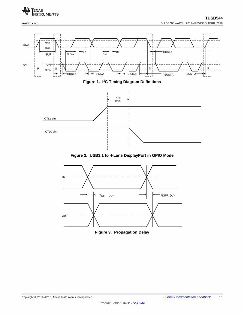
Figure 1. I2C Timing Diagram Definitions
Figure 2. USB3.1 to 4-Lane DisplayPort in GPIO Mode
Figure 3. Propagation Delay

CTL1
VOUT
50%
90%
50%
10%
TAUX_SW_ON TAUX_SW_OFF + TCTL1_DEBOUNCE
tr tf
20%
80%
TIDLEExit TIDLEEntry
IN+
IN-
Vcm
OUT+
OUT-
Vcm
VRX-LFPS-DET-DIFF-PP
12
TUSB544SLLSEZ0E –APRIL 2017–REVISED APRIL 2018 www.ti.com
Product Folder Links: TUSB544
Submit Documentation Feedback Copyright © 2017–2018, Texas Instruments Incorporated
Figure 4. Electrical Idle Mode Exit and Entry Delay
Figure 5. Output Rise and Fall Times
Figure 6. AUX and SBU Switch ON and OFF Timing Diagram
Differential Input Voltage (mVpp)
Diff
eren
tial O
utpu
t Vol
tage
(m
Vpp
)
0 200 400 600 800 1000 1200 1400 1600 1800 20000
200
400
600
800
1000
1200
1400
1600
1800
D010
EQ 0EQ 2EQ 4EQ 6EQ 8EQ 10EQ 12EQ 15
Differential Input Voltage (mVpp)
Diff
eren
tial O
utpu
t Vol
tage
(m
Vpp
)
0 200 400 600 800 1000 1200 1400 1600 1800 20000
200
400
600
800
1000
1200
1400
1600
1800
D008
EQ 0EQ 2EQ 4EQ 6EQ 8EQ 10EQ 12EQ 15
Frequency (GHz)
SD
D11
(dB
)
0 5 10 15 20-45
-40
-35
-30
-25
-20
-15
-10
-5
0
D003Frequency (GHz)
SD
D22
(dB
)
0 5 10 15 20-45
-40
-35
-30
-25
-20
-15
-10
-5
0
D004
Frequency (GHz)
SD
D11
(dB
)
0 5 10 15 20-45
-40
-35
-30
-25
-20
-15
-10
-5
0
D001Frequency (GHz)
SD
D22
(dB
)
0 5 10 15 20-35
-30
-25
-20
-15
-10
-5
0
D002
13
TUSB544www.ti.com SLLSEZ0E –APRIL 2017–REVISED APRIL 2018
Product Folder Links: TUSB544
Submit Documentation FeedbackCopyright © 2017–2018, Texas Instruments Incorporated
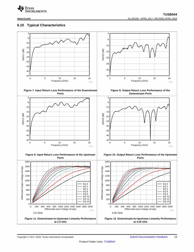
6.10 Typical Characteristics
Figure 7. Input Return Loss Performance of the DownstreamPorts
Figure 8. Output Return Loss Performance of theDownstream Ports
Figure 9. Input Return Loss Performance of the UpstreamPorts
Figure 10. Output Return Loss Performance of the UpstreamPorts
2.5 GHz
Figure 11. Downstream-to-Upstream Linearity Performanceat 2.5 GHz
4.05 GHz
Figure 12. Downstream-to-Upstream Linearity Performanceat 4.05 GHz
Y A
xis
Titl
e (U
nit)
0 200 400 600 800 1000 1200 1400 1600 1800 20000
200
400
600
800
1000
1200
1400
1600
D011
EQ 0EQ 2EQ 4EQ 6EQ 8EQ 10EQ 12EQ 15
Differential Input Voltage (mVpp)
Diff
eren
tial O
utpu
t Vol
tage
(m
Vpp
)
0 200 400 600 800 1000 1200 1400 1600 1800 20000
200
400
600
800
1000
1200
1400
1600
D012
EQ 0
Differential Input Voltage (mVpp)
Diff
eren
tial O
utpu
t Vol
tage
(m
Vpp
)
0 200 400 600 800 1000 1200 1400 1600 1800 20000
200
400
600
800
1000
1200
1400
1600
D009
EQ 0
Differential Input Voltage (mVpp)
Diff
eren
tial O
utpu
t Vol
tage
(m
Vpp
)
0 200 400 600 800 1000 1200 1400 1600 1800 20000
200
400
600
800
1000
1200
1400
1600
1800
D010
EQ 0EQ 2EQ 4EQ 6EQ 8EQ 10EQ 12EQ 15
14
TUSB544SLLSEZ0E –APRIL 2017–REVISED APRIL 2018 www.ti.com
Product Folder Links: TUSB544
Submit Documentation Feedback Copyright © 2017–2018, Texas Instruments Incorporated
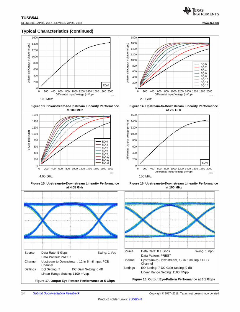
Typical Characteristics (continued)
100 MHz
Figure 13. Downstream-to-Upstream Linearity Performanceat 100 MHz
2.5 GHz
Figure 14. Upstream-to-Downstream Linearity Performanceat 2.5 GHz
4.05 GHz
Figure 15. Upstream-to-Downstream Linearity Performanceat 4.05 GHz
100 MHz
Figure 16. Upstream-to-Downstream Linearity Performanceat 100 MHz
Source Data Rate: 5 Gbps Swing: 1 VppData Pattern: PRBS7
Channel Upstream-to-Downstream, 12 in 6 mil Input PCBChannel
Settings EQ Setting: 7 DC Gain Setting: 0 dBLinear Range Setting: 1100 mVpp
Figure 17. Output Eye-Pattern Performance at 5 Gbps
Source Data Rate: 8.1 Gbps Swing: 1 VppData Pattern: PRBS7
Channel Upstream-to-Downstream, 12 in 6 mil Input PCBChannel
Settings EQ Setting: 7 DC Gain Setting: 0 dBLinear Range Setting: 1100 mVpp
Figure 18. Output Eye-Pattern Performance at 8.1 Gbps
Frequency (GHz)
SD
D21
(dB
)
0.01 0.1 1 10 2020-10
-5
0
5
10
15
D006
EQ0EQ1EQ2EQ3
EQ4EQ5EQ6EQ7
EQ8EQ9EQ10EQ11
EQ12EQ13EQ14EQ15
Frequency (GHz)
SD
D21
(dB
)
0.01 0.1 1 10 2020-10
-5
0
5
10
15
D005
EQ0EQ1EQ2EQ3
EQ4EQ5EQ6EQ7
EQ8EQ9EQ10EQ11
EQ12EQ13EQ14EQ15
15
TUSB544www.ti.com SLLSEZ0E –APRIL 2017–REVISED APRIL 2018
Product Folder Links: TUSB544
Submit Documentation FeedbackCopyright © 2017–2018, Texas Instruments Incorporated
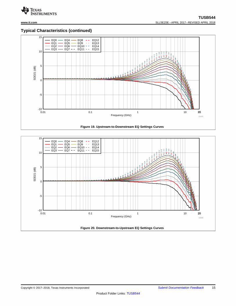
Typical Characteristics (continued)
Figure 19. Upstream-to-Downstream EQ Settings Curves
Figure 20. Downstream-to-Upstream EQ Settings Curves
16
TUSB544SLLSEZ0E –APRIL 2017–REVISED APRIL 2018 www.ti.com
Product Folder Links: TUSB544
Submit Documentation Feedback Copyright © 2017–2018, Texas Instruments Incorporated
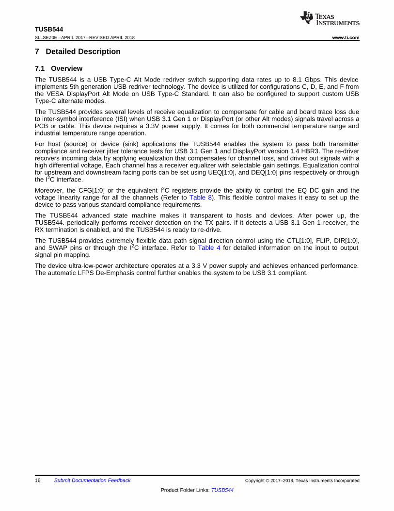
7 Detailed Description
7.1 OverviewThe TUSB544 is a USB Type-C Alt Mode redriver switch supporting data rates up to 8.1 Gbps. This deviceimplements 5th generation USB redriver technology. The device is utilized for configurations C, D, E, and F fromthe VESA DisplayPort Alt Mode on USB Type-C Standard. It can also be configured to support custom USBType-C alternate modes.
The TUSB544 provides several levels of receive equalization to compensate for cable and board trace loss dueto inter-symbol interference (ISI) when USB 3.1 Gen 1 or DisplayPort (or other Alt modes) signals travel across aPCB or cable. This device requires a 3.3V power supply. It comes for both commercial temperature range andindustrial temperature range operation.
For host (source) or device (sink) applications the TUSB544 enables the system to pass both transmittercompliance and receiver jitter tolerance tests for USB 3.1 Gen 1 and DisplayPort version 1.4 HBR3. The re-driverrecovers incoming data by applying equalization that compensates for channel loss, and drives out signals with ahigh differential voltage. Each channel has a receiver equalizer with selectable gain settings. Equalization controlfor upstream and downstream facing ports can be set using UEQ[1:0], and DEQ[1:0] pins respectively or throughthe I2C interface.
Moreover, the CFG[1:0] or the equivalent I2C registers provide the ability to control the EQ DC gain and thevoltage linearity range for all the channels (Refer to Table 8). This flexible control makes it easy to set up thedevice to pass various standard compliance requirements.
The TUSB544 advanced state machine makes it transparent to hosts and devices. After power up, theTUSB544. periodically performs receiver detection on the TX pairs. If it detects a USB 3.1 Gen 1 receiver, theRX termination is enabled, and the TUSB544 is ready to re-drive.
The TUSB544 provides extremely flexible data path signal direction control using the CTL[1:0], FLIP, DIR[1:0],and SWAP pins or through the I2C interface. Refer to Table 4 for detailed information on the input to outputsignal pin mapping.
The device ultra-low-power architecture operates at a 3.3 V power supply and achieves enhanced performance.The automatic LFPS De-Emphasis control further enables the system to be USB 3.1 compliant.
I2C_EN
UEQ1/A1
UEQ0/A0
SBU2
SBU1
CTL0/SDA
FLIP/SCL
VCC
AUXp
AUXn
DEQ[1:0]
VIO_SEL
M
U
X
VREG
FSM, Control Logic &
Registers
DRX[2:1]EQ_SEL
CTL1
AU
X
RX
I2C
Slave
DTX2p
DRX1p
DRX2p
DTX2n
DRX1n
DRX2n
DTX1p
DTX1n
UTX2p
URX1p
URX2p
URX2n
UTX1n
Driver
EQ
Te
rmT
erm
DRX2EQ_SEL
Te
rm
URX2EQ_SEL
EQEQ
Driver
Te
rm
De
tect
Driver
EQ
Te
rmT
erm
DTX2EQ_SEL
Te
rm
UTX2EQ_SEL
EQEQ
DriverT
erm
UTX2n
Driver
EQ
Te
rmT
erm
DTX1EQ_SEL
Te
rm
UTX1EQ_SEL
EQEQ
Driver
Te
rm
De
tect
UTX1p
Driver
EQ
Te
rmT
erm
DRX1EQ_SEL
Te
rm
URX1EQ_SEL
EQEQ
Driver
Te
rm
De
tect
URX1n
De
tect
CFG[1:0]
SWAP
SLP_S0#
De
tect
De
tect
De
tect
De
tect
DTX[2:1]EQ_SEL
URX[2:1]EQ_SEL
UTX[2:1]EQ_SEL
DIR[1:0]
CHANNEL 0 CHANNEL 0
CHANNEL 1 CHANNEL 1
CHANNEL 2 CHANNEL 2
CHANNEL 3 CHANNEL 3
17
TUSB544www.ti.com SLLSEZ0E –APRIL 2017–REVISED APRIL 2018
Product Folder Links: TUSB544
Submit Documentation FeedbackCopyright © 2017–2018, Texas Instruments Incorporated
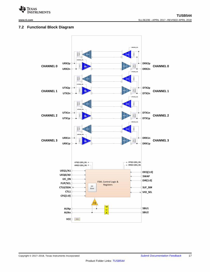
7.2 Functional Block Diagram
18
TUSB544SLLSEZ0E –APRIL 2017–REVISED APRIL 2018 www.ti.com
Product Folder Links: TUSB544
Submit Documentation Feedback Copyright © 2017–2018, Texas Instruments Incorporated
7.3 Feature Description
7.3.1 USB 3.1The TUSB544 supports USB 3.1 data rates up to 5 Gbps. The TUSB544 supports all the USB defined powerstates (U0, U1, U2, and U3). Because the TUSB544 is a linear redriver, it can’t decode USB3.1 physical layertraffic. The TUSB544 monitors the actual physical layer conditions like receiver termination, electrical idle, LFPS,and SuperSpeed signaling rate to determine the USB power state of the USB3.1 interface.
The TUSB544 features an intelligent low frequency periodic signaling (LFPS) detector. The LFPS detectorautomatically senses the low frequency signals and disables receiver equalization functionality. When notreceiving LFPS, the TUSB544 will enable receiver equalization based on the UEQ[1:0] and DEQ[1:0] pins orvalues programmed into UEQ[3:0]_SEL, and DEQ[3:0]_SEL registers.
7.3.2 DisplayPortThe TUSB544 supports up to 4 DisplayPort lanes at data rates up to 8.1Gbps (HBR3). The TUSB544, whenconfigured in DisplayPort mode, monitors the native AUX traffic as it traverses between DisplayPort source andDisplayPort sink. For the purposes of reducing power, the TUSB544 will manage the number of activeDisplayPort lanes based on the content of the AUX transactions. The TUSB544 snoops native AUX writes toDisplayPort sink’s DPCD registers 00101h (LANE_COUNT_SET) and 00600h (SET_POWER_STATE).TUSB544 will disable/enable lanes based on value written to LANE_COUNT_SET. The TUSB544 will disable alllanes when SET_POWER_STATE is in the D3. Otherwise active lanes will be based on value ofLANE_COUNT_SET.
DisplayPort AUX snooping is enabled by default but can be disabled by changing the AUX_SNOOP_DISABLEregister. Once AUX snoop is disabled, management of TUSB544’s DisplayPort lanes are controlled throughvarious configuration registers.
7.3.3 4-Level InputsThe TUSB544 has (I2C_EN, UEQ[1:0], DEQ[1:0], CFG[1:0], and A[1:0]) 4-level inputs pins that are used tocontrol the equalization gain, voltage linearity range, and place TUSB544 into different modes of operation.These 4-level inputs utilize a resistor divider to help set the 4 valid levels and provide a wider range of controlsettings. There are internal pull-up and a pull-down resisters. These resistors together with the external resistorconnection combine to achieve the desired voltage level.
Table 1. 4-Level Control Pin SettingsLEVEL SETTINGS
0 Option 1: Tie 1 KΩ 5% to GND.Option 2: Tie directly to GND.
R Tie 20 KΩ 5% to GND.F Float (leave pin open)
1 Option 1: Tie 1 KΩ 5%to VCC.Option 2: Tie directly to VCC.
NOTEAll four-level inputs are latched on rising edge of internal reset. After Tcfg_hd, the internalpull-up and pull-down resistors will be isolated in order to save power.
7.3.4 Receiver Linear EqualizationThe purpose of receiver equalization is to compensate for channel insertion loss and inter-symbol interference inthe system. The receiver overcomes these losses by attenuating the low frequency components of the signalswith respect to the high frequency components. The proper gain setting should be selected to match the channelinsertion loss. Two 4-level input pins enable up to 16 possible equalization settings. The upstream path, and thedownstream path each have their own two 4-level inputs for equalization settings; UEQ[1:0] and DEQ[1:0]respectively. The TUSB544 also provides the flexibility of adjusting equalization settings through I2C registersURX[2:1]EQ_SEL, UTX[2:1]EQ_SEL, DRX[2:1]EQ_SEL, and DTX[2:1]EQ_SEL for each individual channel andfor each direction (upstream or downstream) .
19
TUSB544www.ti.com SLLSEZ0E –APRIL 2017–REVISED APRIL 2018
Product Folder Links: TUSB544
Submit Documentation FeedbackCopyright © 2017–2018, Texas Instruments Incorporated
7.4 Device Functional Modes
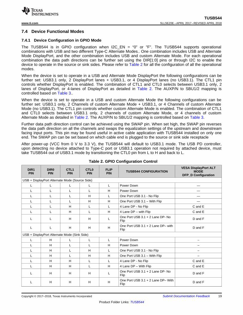
7.4.1 Device Configuration in GPIO ModeThe TUSB544 is in GPIO configuration when I2C_EN = “0” or "F". The TUSB544 supports operationalcombinations with USB and two different Type-C Alternate Modes.. One combination includes USB and AlternateMode DisplayPort, and the other combination includes USB and custom Alternate Mode. For each operationalcombination the data path directions can be further set using the DIR[1:0] pins or through I2C to enable thedevice to operate in the source or sink sides. Please refer to Table 2 for all the configuration of all the operationalmodes.
When the device is set to operate in a USB and Alternate Mode DisplayPort the following configurations can befurther set: USB3.1 only, 2 DisplayPort lanes + USB3.1, or 4 DisplayPort lanes (no USB3.1). The CTL1 pincontrols whether DisplayPort is enabled. The combination of CTL1 and CTL0 selects between USB3.1 only, 2lanes of DisplayPort, or 4-lanes of DisplayPort as detailed in Table 2. The AUXP/N to SBU1/2 mapping iscontrolled based on Table 3..
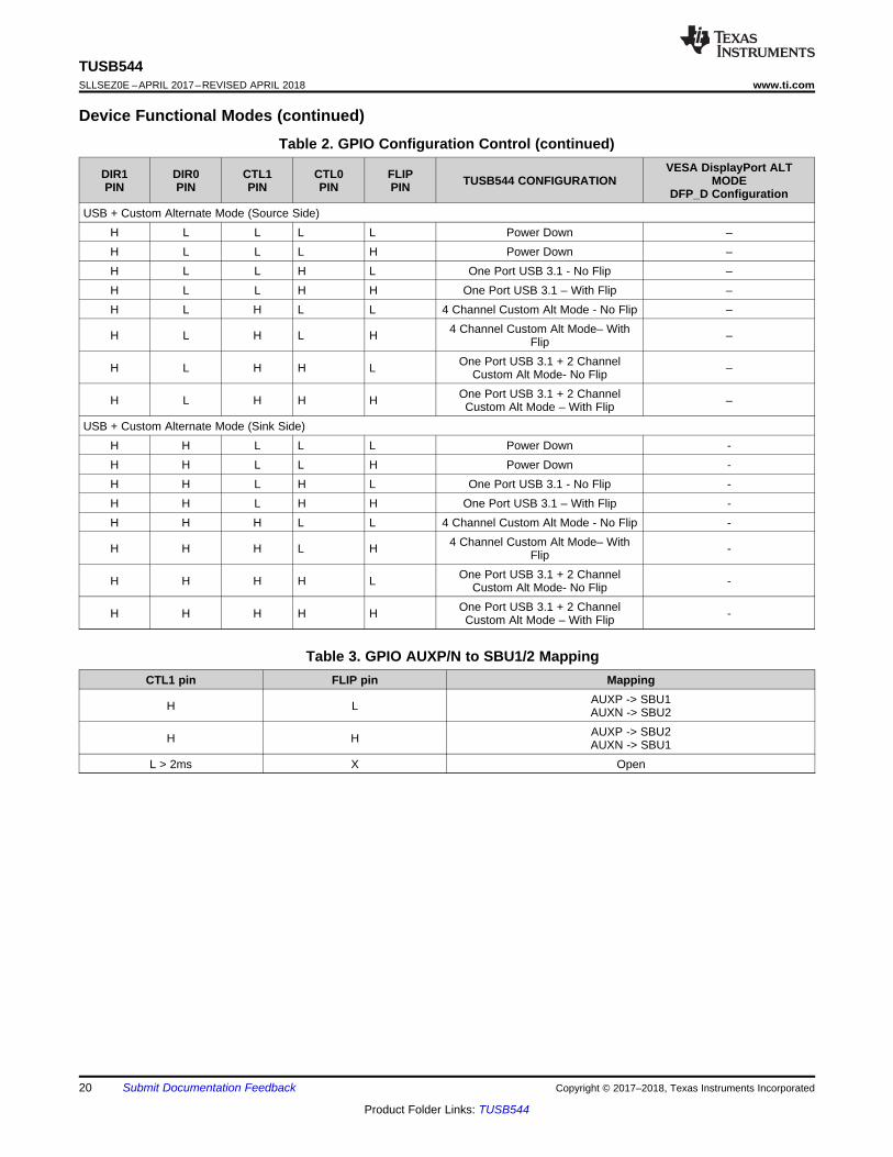
When the device is set to operate in a USB and custom Alternate Mode the following configurations can befurther set: USB3.1 only, 2 Channels of custom Alternate Mode + USB3.1, or 4 Channels of custom AlternateMode (no USB3.1). The CTL1 pin controls whether custom Alternate Mode is enabled. The combination of CTL1and CTL0 selects between USB3.1 only, 2 channels of custom Alternate Mode, or 4 channels of customAlternate Mode as detailed in Table 2. The AUXP/N to SBU1/2 mapping is controlled based on Table 3.
Further data path direction control can be achieved using the SWAP pin. When set high, the SWAP pin reversesthe data path direction on all the channels and swaps the equalization settings of the upstream and downstreamfacing input ports. This pin may be found useful in active cable application with TUSB544 installed on only oneend. The SWAP pin can be set based on which cable end is plugged to the source or sink side receptacle
After power-up (VCC from 0 V to 3.3 V), the TUSB544 will default to USB3.1 mode. The USB PD controller,upon detecting no device attached to Type-C port or USB3.1 operation not required by attached device, musttake TUSB544 out of USB3.1 mode by transitioning the CTL0 pin from L to H and back to L.
Table 2. GPIO Configuration Control
DIR1PIN
DIR0PIN
CTL1PIN
CTL0PIN
FLIPPIN TUSB544 CONFIGURATION
VESA DisplayPort ALTMODE
DFP_D ConfigurationUSB + DisplayPort Alternate Mode (Source Side)
L L L L L Power Down —L L L L H Power Down —L L L H L One Port USB 3.1 - No Flip —L L L H H One Port USB 3.1 – With Flip —L L H L L 4 Lane DP - No Flip C and EL L H L H 4 Lane DP – with Flip C and E
L L H H L One Port USB 3.1 + 2 Lane DP- NoFlip D and F
L L H H H One Port USB 3.1 + 2 Lane DP– withFlip D and F
USB + DisplayPort Alternate Mode (Sink Side)L H L L L Power Down –L H L L H Power Down –L H L H L One Port USB 3.1 - No Flip –L H L H H One Port USB 3.1 – With Flip –L H H L L 4 Lane DP - No Flip C and EL H H L H 4 Lane DP – With Flip C and E
L H H H L One Port USB 3.1 + 2 Lane DP- NoFlip D and F
L H H H H One Port USB 3.1 + 2 Lane DP– WithFlip D and F
20
TUSB544SLLSEZ0E –APRIL 2017–REVISED APRIL 2018 www.ti.com
Product Folder Links: TUSB544
Submit Documentation Feedback Copyright © 2017–2018, Texas Instruments Incorporated
Device Functional Modes (continued)Table 2. GPIO Configuration Control (continued)
DIR1PIN
DIR0PIN
CTL1PIN
CTL0PIN
FLIPPIN TUSB544 CONFIGURATION
VESA DisplayPort ALTMODE
DFP_D ConfigurationUSB + Custom Alternate Mode (Source Side)
H L L L L Power Down –H L L L H Power Down –H L L H L One Port USB 3.1 - No Flip –H L L H H One Port USB 3.1 – With Flip –H L H L L 4 Channel Custom Alt Mode - No Flip –
H L H L H 4 Channel Custom Alt Mode– WithFlip –
H L H H L One Port USB 3.1 + 2 ChannelCustom Alt Mode- No Flip –
H L H H H One Port USB 3.1 + 2 ChannelCustom Alt Mode – With Flip –
USB + Custom Alternate Mode (Sink Side)H H L L L Power Down -H H L L H Power Down -H H L H L One Port USB 3.1 - No Flip -H H L H H One Port USB 3.1 – With Flip -H H H L L 4 Channel Custom Alt Mode - No Flip -
H H H L H 4 Channel Custom Alt Mode– WithFlip -
H H H H L One Port USB 3.1 + 2 ChannelCustom Alt Mode- No Flip -
H H H H H One Port USB 3.1 + 2 ChannelCustom Alt Mode – With Flip -
Table 3. GPIO AUXP/N to SBU1/2 MappingCTL1 pin FLIP pin Mapping
H L AUXP -> SBU1AUXN -> SBU2
H H AUXP -> SBU2AUXN -> SBU1
L > 2ms X Open
21
TUSB544www.ti.com SLLSEZ0E –APRIL 2017–REVISED APRIL 2018
Product Folder Links: TUSB544
Submit Documentation FeedbackCopyright © 2017–2018, Texas Instruments Incorporated
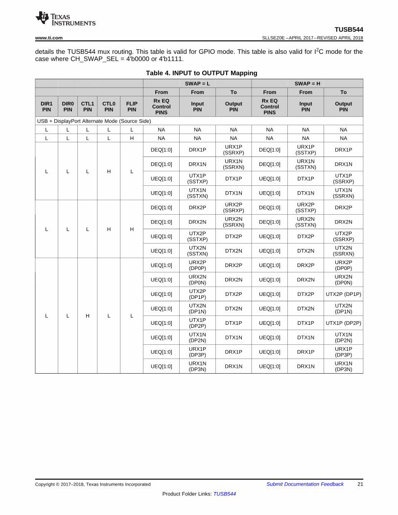
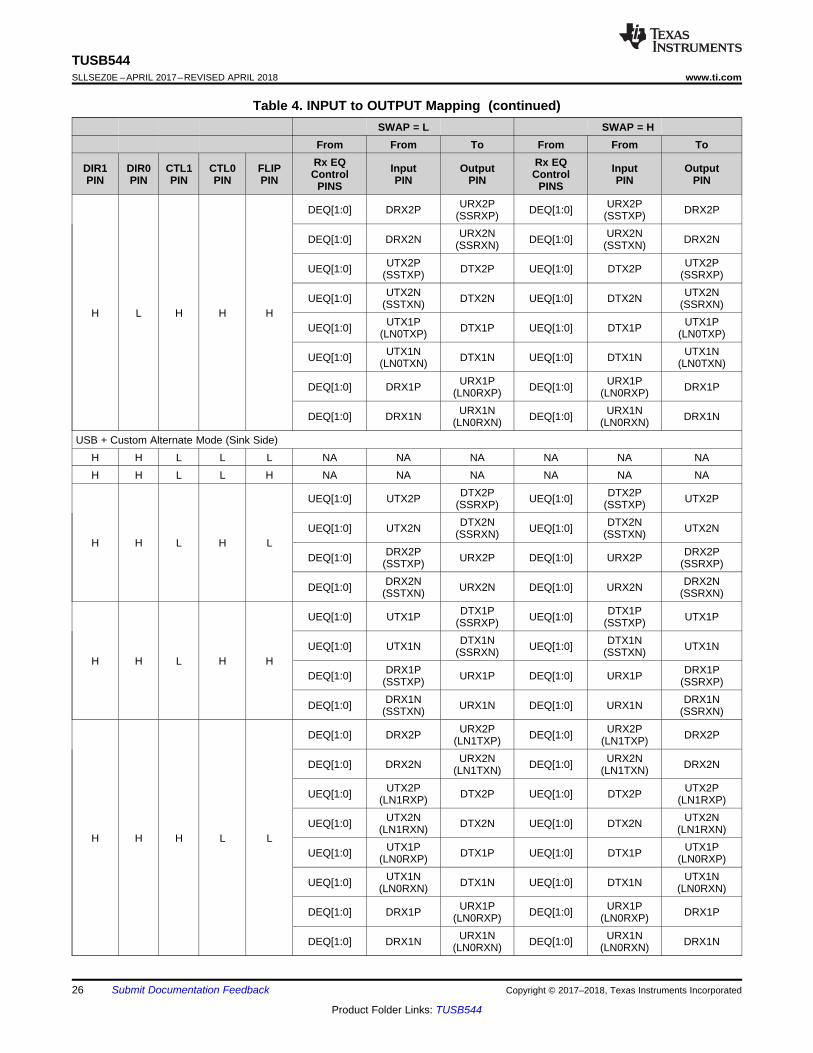
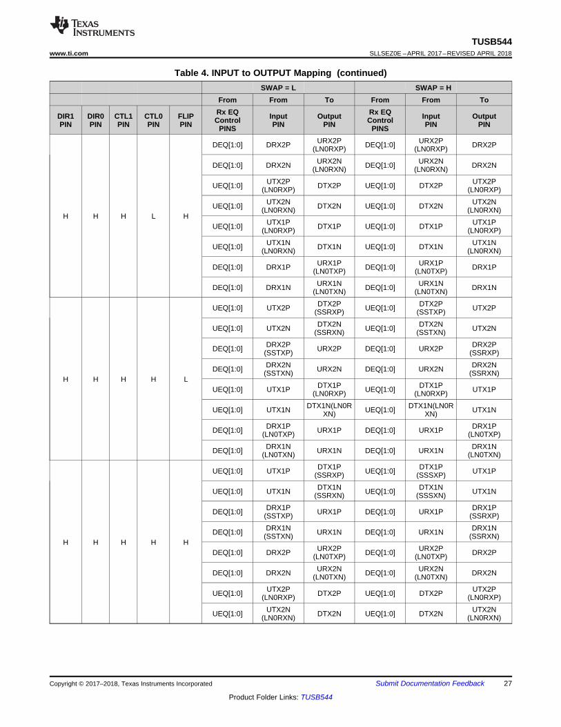
details the TUSB544 mux routing. This table is valid for GPIO mode. This table is also valid for I2C mode for thecase where CH_SWAP_SEL = 4'b0000 or 4'b1111.
Table 4. INPUT to OUTPUT MappingSWAP = L SWAP = H
From From To From From To
DIR1PIN
DIR0PIN
CTL1PIN
CTL0PIN
FLIPPIN
Rx EQControl
PINSInputPIN
OutputPIN
Rx EQControl
PINSInputPIN
OutputPIN
USB + DisplayPort Alternate Mode (Source Side)L L L L L NA NA NA NA NA NAL L L L H NA NA NA NA NA NA
L L L H L
DEQ[1:0] DRX1P URX1P(SSRXP) DEQ[1:0] URX1P
(SSTXP) DRX1P
DEQ[1:0] DRX1N URX1N(SSRXN) DEQ[1:0] URX1N
(SSTXN) DRX1N
UEQ[1:0] UTX1P(SSTXP) DTX1P UEQ[1:0] DTX1P UTX1P
(SSRXP)
UEQ[1:0] UTX1N(SSTXN) DTX1N UEQ[1:0] DTX1N UTX1N
(SSRXN)
L L L H H
DEQ[1:0] DRX2P URX2P(SSRXP) DEQ[1:0] URX2P
(SSTXP) DRX2P
DEQ[1:0] DRX2N URX2N(SSRXN) DEQ[1:0] URX2N
(SSTXN) DRX2N
UEQ[1:0] UTX2P(SSTXP) DTX2P UEQ[1:0] DTX2P UTX2P
(SSRXP)
UEQ[1:0] UTX2N(SSTXN) DTX2N UEQ[1:0] DTX2N UTX2N
(SSRXN)
L L H L L
UEQ[1:0] URX2P(DP0P) DRX2P UEQ[1:0] DRX2P URX2P
(DP0P)
UEQ[1:0] URX2N(DP0N) DRX2N UEQ[1:0] DRX2N URX2N
(DP0N)
UEQ[1:0] UTX2P(DP1P) DTX2P UEQ[1:0] DTX2P UTX2P (DP1P)
UEQ[1:0] UTX2N(DP1N) DTX2N UEQ[1:0] DTX2N UTX2N
(DP1N)
UEQ[1:0] UTX1P(DP2P) DTX1P UEQ[1:0] DTX1P UTX1P (DP2P)
UEQ[1:0] UTX1N(DP2N) DTX1N UEQ[1:0] DTX1N UTX1N
(DP2N)
UEQ[1:0] URX1P(DP3P) DRX1P UEQ[1:0] DRX1P URX1P
(DP3P)
UEQ[1:0] URX1N(DP3N) DRX1N UEQ[1:0] DRX1N URX1N
(DP3N)
22
TUSB544SLLSEZ0E –APRIL 2017–REVISED APRIL 2018 www.ti.com
Product Folder Links: TUSB544
Submit Documentation Feedback Copyright © 2017–2018, Texas Instruments Incorporated
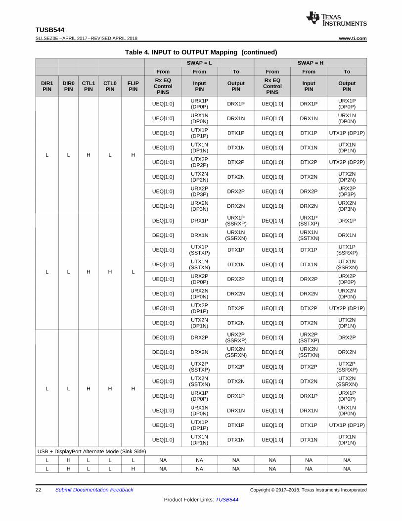
Table 4. INPUT to OUTPUT Mapping (continued)SWAP = L SWAP = H
From From To From From To
DIR1PIN
DIR0PIN
CTL1PIN
CTL0PIN
FLIPPIN
Rx EQControl
PINSInputPIN
OutputPIN
Rx EQControl
PINSInputPIN
OutputPIN
L L H L H
UEQ[1:0] URX1P(DP0P) DRX1P UEQ[1:0] DRX1P URX1P
(DP0P)
UEQ[1:0] URX1N(DP0N) DRX1N UEQ[1:0] DRX1N URX1N
(DP0N)
UEQ[1:0] UTX1P(DP1P) DTX1P UEQ[1:0] DTX1P UTX1P (DP1P)
UEQ[1:0] UTX1N(DP1N) DTX1N UEQ[1:0] DTX1N UTX1N
(DP1N)
UEQ[1:0] UTX2P(DP2P) DTX2P UEQ[1:0] DTX2P UTX2P (DP2P)
UEQ[1:0] UTX2N(DP2N) DTX2N UEQ[1:0] DTX2N UTX2N
(DP2N)
UEQ[1:0] URX2P(DP3P) DRX2P UEQ[1:0] DRX2P URX2P
(DP3P)
UEQ[1:0] URX2N(DP3N) DRX2N UEQ[1:0] DRX2N URX2N
(DP3N)
L L H H L
DEQ[1:0] DRX1P URX1P(SSRXP) DEQ[1:0] URX1P
(SSTXP) DRX1P
DEQ[1:0] DRX1N URX1N(SSRXN) DEQ[1:0] URX1N
(SSTXN) DRX1N
UEQ[1:0] UTX1P(SSTXP) DTX1P UEQ[1:0] DTX1P UTX1P
(SSRXP)
UEQ[1:0] UTX1N(SSTXN) DTX1N UEQ[1:0] DTX1N UTX1N
(SSRXN)
UEQ[1:0] URX2P(DP0P) DRX2P UEQ[1:0] DRX2P URX2P
(DP0P)
UEQ[1:0] URX2N(DP0N) DRX2N UEQ[1:0] DRX2N URX2N
(DP0N)
UEQ[1:0] UTX2P(DP1P) DTX2P UEQ[1:0] DTX2P UTX2P (DP1P)
UEQ[1:0] UTX2N(DP1N) DTX2N UEQ[1:0] DTX2N UTX2N
(DP1N)
L L H H H
DEQ[1:0] DRX2P URX2P(SSRXP) DEQ[1:0] URX2P
(SSTXP) DRX2P
DEQ[1:0] DRX2N URX2N(SSRXN) DEQ[1:0] URX2N
(SSTXN) DRX2N
UEQ[1:0] UTX2P(SSTXP) DTX2P UEQ[1:0] DTX2P UTX2P
(SSRXP)
UEQ[1:0] UTX2N(SSTXN) DTX2N UEQ[1:0] DTX2N UTX2N
(SSRXN)
UEQ[1:0] URX1P(DP0P) DRX1P UEQ[1:0] DRX1P URX1P
(DP0P)
UEQ[1:0] URX1N(DP0N) DRX1N UEQ[1:0] DRX1N URX1N
(DP0N)
UEQ[1:0] UTX1P(DP1P) DTX1P UEQ[1:0] DTX1P UTX1P (DP1P)
UEQ[1:0] UTX1N(DP1N) DTX1N UEQ[1:0] DTX1N UTX1N
(DP1N)USB + DisplayPort Alternate Mode (Sink Side)
L H L L L NA NA NA NA NA NAL H L L H NA NA NA NA NA NA
23
TUSB544www.ti.com SLLSEZ0E –APRIL 2017–REVISED APRIL 2018
Product Folder Links: TUSB544
Submit Documentation FeedbackCopyright © 2017–2018, Texas Instruments Incorporated
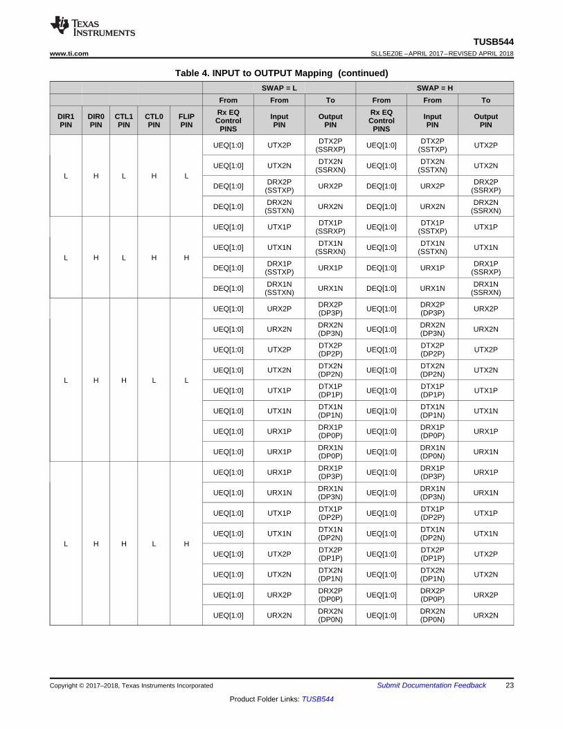
Table 4. INPUT to OUTPUT Mapping (continued)SWAP = L SWAP = H
From From To From From To
DIR1PIN
DIR0PIN
CTL1PIN
CTL0PIN
FLIPPIN
Rx EQControl
PINSInputPIN
OutputPIN
Rx EQControl
PINSInputPIN
OutputPIN
L H L H L
UEQ[1:0] UTX2P DTX2P(SSRXP) UEQ[1:0] DTX2P
(SSTXP) UTX2P
UEQ[1:0] UTX2N DTX2N(SSRXN) UEQ[1:0] DTX2N
(SSTXN) UTX2N
DEQ[1:0] DRX2P(SSTXP) URX2P DEQ[1:0] URX2P DRX2P
(SSRXP)
DEQ[1:0] DRX2N(SSTXN) URX2N DEQ[1:0] URX2N DRX2N
(SSRXN)
L H L H H
UEQ[1:0] UTX1P DTX1P(SSRXP) UEQ[1:0] DTX1P
(SSTXP) UTX1P
UEQ[1:0] UTX1N DTX1N(SSRXN) UEQ[1:0] DTX1N
(SSTXN) UTX1N
DEQ[1:0] DRX1P(SSTXP) URX1P DEQ[1:0] URX1P DRX1P
(SSRXP)
DEQ[1:0] DRX1N(SSTXN) URX1N DEQ[1:0] URX1N DRX1N
(SSRXN)
L H H L L
UEQ[1:0] URX2P DRX2P(DP3P) UEQ[1:0] DRX2P
(DP3P) URX2P
UEQ[1:0] URX2N DRX2N(DP3N) UEQ[1:0] DRX2N
(DP3N) URX2N
UEQ[1:0] UTX2P DTX2P(DP2P) UEQ[1:0] DTX2P
(DP2P) UTX2P
UEQ[1:0] UTX2N DTX2N(DP2N) UEQ[1:0] DTX2N
(DP2N) UTX2N
UEQ[1:0] UTX1P DTX1P(DP1P) UEQ[1:0] DTX1P
(DP1P) UTX1P
UEQ[1:0] UTX1N DTX1N(DP1N) UEQ[1:0] DTX1N
(DP1N) UTX1N
UEQ[1:0] URX1P DRX1P(DP0P) UEQ[1:0] DRX1P
(DP0P) URX1P
UEQ[1:0] URX1P DRX1N(DP0P) UEQ[1:0] DRX1N
(DP0N) URX1N
L H H L H
UEQ[1:0] URX1P DRX1P(DP3P) UEQ[1:0] DRX1P
(DP3P) URX1P
UEQ[1:0] URX1N DRX1N(DP3N) UEQ[1:0] DRX1N
(DP3N) URX1N
UEQ[1:0] UTX1P DTX1P(DP2P) UEQ[1:0] DTX1P
(DP2P) UTX1P
UEQ[1:0] UTX1N DTX1N(DP2N) UEQ[1:0] DTX1N
(DP2N) UTX1N
UEQ[1:0] UTX2P DTX2P(DP1P) UEQ[1:0] DTX2P
(DP1P) UTX2P
UEQ[1:0] UTX2N DTX2N(DP1N) UEQ[1:0] DTX2N
(DP1N) UTX2N
UEQ[1:0] URX2P DRX2P(DP0P) UEQ[1:0] DRX2P
(DP0P) URX2P
UEQ[1:0] URX2N DRX2N(DP0N) UEQ[1:0] DRX2N
(DP0N) URX2N

24
TUSB544SLLSEZ0E –APRIL 2017–REVISED APRIL 2018 www.ti.com
Product Folder Links: TUSB544
Submit Documentation Feedback Copyright © 2017–2018, Texas Instruments Incorporated
Table 4. INPUT to OUTPUT Mapping (continued)SWAP = L SWAP = H
From From To From From To
DIR1PIN
DIR0PIN
CTL1PIN
CTL0PIN
FLIPPIN
Rx EQControl
PINSInputPIN
OutputPIN
Rx EQControl
PINSInputPIN
OutputPIN
L H H H L
DEQ[1:0] DRX2P(SSRXP) URX2P DEQ[1:0] URX2P DRX2P
(SSRXP)
DEQ[1:0] DRX2N(SSRXN) URX2N DEQ[1:0] URX2N DRX2N
(SSRXN)
UEQ[1:0] UTX2P DTX2P(SSTXP) UEQ[1:0] DTX2P
(SSTXP) UTX2P
UEQ[1:0] UTX2N DTX2N(SSTXN) UEQ[1:0] DTX2N
(SSTXN) UTX2N
UEQ[1:0] URX1P DRX1P(DP0P) UEQ[1:0] DRX1P
(DP0P) URX1P
UEQ[1:0] URX1N DRX1N(DP0N) UEQ[1:0] DRX1N
(DP0N) URX1N
UEQ[1:0] UTX1P DTX1P(DP1P) UEQ[1:0] DTX1P
(DP1P) UTX1P
UEQ[1:0] UTX1N DTX1N(DP1N) UEQ[1:0] DTX1N
(DP1N) UTX1N
L H H H H
DEQ[1:0] DRX1P(SSRXP) URX1P DEQ[1:0] URX1P DRX1P
(SSRXP)
DEQ[1:0] DRX1N(SSRXN) URX1N DEQ[1:0] URX1N DRX1N
(SSRXN)
UEQ[1:0] UTX1P DTX1P(SSTXP) UEQ[1:0] DTX1P
(SSTXP) UTX1P
UEQ[1:0] UTX1N DTX1N(SSTXN) UEQ[1:0] DTX1N
(SSTXN) UTX1N
UEQ[1:0] URX2P DRX2P(DP0P) UEQ[1:0] DRX2P
(DP0P) URX2P
UEQ[1:0] URX2N DRX2N(DP0N) UEQ[1:0] DRX2N
(DP0N) URX2N
UEQ[1:0] UTX2P DTX2P(DP1P) UEQ[1:0] DTX2P
(DP1P) UTX2P
UEQ[1:0] UTX2N DTX2N(DP1N) UEQ[1:0] DTX2N
(DP1N) UTX2N
USB + Custom Alternate Mode (Source Side)H L L L L NA NA NA NA NA NAH L L L H NA NA NA NA NA NA
H L L H L
DEQ[1:0] DRX1P URX1P(SSRXP) DEQ[1:0] URX1P
(SSTXP) DRX1P
DEQ[1:0] DRX1N URX1N(SSRXN) DEQ[1:0] URX1N
(SSTXN) DRX1N
UEQ[1:0] UTX1P(SSTXP) DTX1P UEQ[1:0] DTX1P UTX1P
(SSRXP)
UEQ[1:0] UTX1N(SSTXN) DTX1N UEQ[1:0] DTX1N UTX1N
(SSRXN)
H L L H H
DEQ[1:0] DRX2P URX2P(SSRXP) DEQ[1:0] URX2P
(SSTXP) DRX2P
DEQ[1:0] DRX2N URX2N(SSRXN) DEQ[1:0] URX2N
(SSTXN) DRX2N
UEQ[1:0] UTX2P(SSTXP) DTX2P UEQ[1:0] DTX2P UTX2P
(SSRXP)
UEQ[1:0] UTX2N(SSTXN) DTX2N UEQ[1:0] DTX2N UTX2N
(SSRXN)
25
TUSB544www.ti.com SLLSEZ0E –APRIL 2017–REVISED APRIL 2018
Product Folder Links: TUSB544
Submit Documentation FeedbackCopyright © 2017–2018, Texas Instruments Incorporated
Table 4. INPUT to OUTPUT Mapping (continued)SWAP = L SWAP = H
From From To From From To
DIR1PIN
DIR0PIN
CTL1PIN
CTL0PIN
FLIPPIN
Rx EQControl
PINSInputPIN
OutputPIN
Rx EQControl
PINSInputPIN
OutputPIN
H L H L L
DEQ[1:0] DRX2P URX2P(LN1RXP) DEQ[1:0] URX2P
(LN1RXP) DRX2P
DEQ[1:0] DRX2N URX2N(LN1RXN) DEQ[1:0] URX2N
(LN1RXN) DRX2N
UEQ[1:0] UTX2P(LN1TXP) DTX2P UEQ[1:0] DTX2P UTX2P
(LN1TXP)
UEQ[1:0] UTX2N(LN1TXN) DTX2N UEQ[1:0] DTX2N UTX2N
(LN1TXN)
UEQ[1:0] UTX1P(LN0TXP) DTX1P UEQ[1:0] DTX1P UTX1P
(LN0TXP)
UEQ[1:0] UTX1N(LN0TXN) DTX1N UEQ[1:0] DTX1N UTX1N
(LN0TXN)
DEQ[1:0] DRX1P URX1P(LN0RXP) DEQ[1:0] URX1P
(LN0RXP) DRX1P
DEQ[1:0] DRX1N URX1N(LN0RXN) DEQ[1:0] URX1N
(LN0RXN) DRX1N
H L H L H
DEQ[1:0] DRX1P URX1P(LN1RXP) DEQ[1:0] URX1P
(LN1RXP) DRX1P
DEQ[1:0] DRX1N URX1N(LN1RXN) DEQ[1:0] URX1N
(LN1RXN) DRX1N
UEQ[1:0] UTX1P(LN1TXP) DTX1P UEQ[1:0] DTX1P UTX1P
(LN1TXP)
UEQ[1:0] UTX1N(LN1TXN) DTX1N UEQ[1:0] DTX1N UTX1N
(LN1TXN)
UEQ[1:0] UTX2P(LN0TXP) DTX2P UEQ[1:0] DTX2P UTX2P
(LN0TXP)
UEQ[1:0] UTX2N(LN0TXN) DTX2N UEQ[1:0] DTX2N UTX2N
(LN0TXN)
H L H H L
DEQ[1:0] DRX2P URX2P(LN0RXP) DEQ[1:0] URX2P
(LN0RXP) DRX2P
DEQ[1:0] DRX2N URX2N(LN0RXN) DEQ[1:0] URX2N
(LN0RXN) DRX2N
DEQ[1:0] DRX1P URX1P(SSRXP) DEQ[1:0] URX1P
(SSTXP) DRX1P
DEQ[1:0] DRX1N URX1N(SSRXN) DEQ[1:0] URX1N
(SSTXN) DRX1N
UEQ[1:0] UTX1P(SSTXP) DTX1P UEQ[1:0] DTX1P UTX1P
(SSRXP)
UEQ[1:0] UTX1N(SSTXN) DTX1N UEQ[1:0] DTX1N UTX1N
(SSRXN)
UEQ[1:0] UTX2P(LN0TXP) DTX2P UEQ[1:0] DTX2P UTX2P
(LN0TXP)
UEQ[1:0] UTX2N(LN0TXN) DTX2N UEQ[1:0] DTX2N UTX2N
(LN0TXN)
DEQ[1:0] DRX2P URX2P(LN0RXP) DEQ[1:0] URX2P
(LN0RXP) DRX2P
DEQ[1:0] DRX2N URX2N(LN0RXN) DEQ[1:0] URX2N
(LN0RXN) DRX2N
26
TUSB544SLLSEZ0E –APRIL 2017–REVISED APRIL 2018 www.ti.com
Product Folder Links: TUSB544
Submit Documentation Feedback Copyright © 2017–2018, Texas Instruments Incorporated
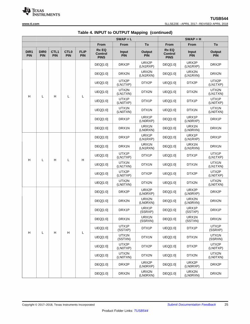
Table 4. INPUT to OUTPUT Mapping (continued)SWAP = L SWAP = H
From From To From From To
DIR1PIN
DIR0PIN
CTL1PIN
CTL0PIN
FLIPPIN
Rx EQControl
PINSInputPIN
OutputPIN
Rx EQControl
PINSInputPIN
OutputPIN
H L H H H
DEQ[1:0] DRX2P URX2P(SSRXP) DEQ[1:0] URX2P
(SSTXP) DRX2P
DEQ[1:0] DRX2N URX2N(SSRXN) DEQ[1:0] URX2N
(SSTXN) DRX2N
UEQ[1:0] UTX2P(SSTXP) DTX2P UEQ[1:0] DTX2P UTX2P
(SSRXP)
UEQ[1:0] UTX2N(SSTXN) DTX2N UEQ[1:0] DTX2N UTX2N
(SSRXN)
UEQ[1:0] UTX1P(LN0TXP) DTX1P UEQ[1:0] DTX1P UTX1P
(LN0TXP)
UEQ[1:0] UTX1N(LN0TXN) DTX1N UEQ[1:0] DTX1N UTX1N
(LN0TXN)
DEQ[1:0] DRX1P URX1P(LN0RXP) DEQ[1:0] URX1P
(LN0RXP) DRX1P
DEQ[1:0] DRX1N URX1N(LN0RXN) DEQ[1:0] URX1N
(LN0RXN) DRX1N
USB + Custom Alternate Mode (Sink Side)H H L L L NA NA NA NA NA NAH H L L H NA NA NA NA NA NA
H H L H L
UEQ[1:0] UTX2P DTX2P(SSRXP) UEQ[1:0] DTX2P
(SSTXP) UTX2P
UEQ[1:0] UTX2N DTX2N(SSRXN) UEQ[1:0] DTX2N
(SSTXN) UTX2N
DEQ[1:0] DRX2P(SSTXP) URX2P DEQ[1:0] URX2P DRX2P
(SSRXP)
DEQ[1:0] DRX2N(SSTXN) URX2N DEQ[1:0] URX2N DRX2N
(SSRXN)
H H L H H
UEQ[1:0] UTX1P DTX1P(SSRXP) UEQ[1:0] DTX1P
(SSTXP) UTX1P
UEQ[1:0] UTX1N DTX1N(SSRXN) UEQ[1:0] DTX1N
(SSTXN) UTX1N
DEQ[1:0] DRX1P(SSTXP) URX1P DEQ[1:0] URX1P DRX1P
(SSRXP)
DEQ[1:0] DRX1N(SSTXN) URX1N DEQ[1:0] URX1N DRX1N
(SSRXN)
H H H L L
DEQ[1:0] DRX2P URX2P(LN1TXP) DEQ[1:0] URX2P
(LN1TXP) DRX2P
DEQ[1:0] DRX2N URX2N(LN1TXN) DEQ[1:0] URX2N
(LN1TXN) DRX2N
UEQ[1:0] UTX2P(LN1RXP) DTX2P UEQ[1:0] DTX2P UTX2P
(LN1RXP)
UEQ[1:0] UTX2N(LN1RXN) DTX2N UEQ[1:0] DTX2N UTX2N
(LN1RXN)
UEQ[1:0] UTX1P(LN0RXP) DTX1P UEQ[1:0] DTX1P UTX1P
(LN0RXP)
UEQ[1:0] UTX1N(LN0RXN) DTX1N UEQ[1:0] DTX1N UTX1N
(LN0RXN)
DEQ[1:0] DRX1P URX1P(LN0RXP) DEQ[1:0] URX1P
(LN0RXP) DRX1P
DEQ[1:0] DRX1N URX1N(LN0RXN) DEQ[1:0] URX1N
(LN0RXN) DRX1N
27
TUSB544www.ti.com SLLSEZ0E –APRIL 2017–REVISED APRIL 2018
Product Folder Links: TUSB544
Submit Documentation FeedbackCopyright © 2017–2018, Texas Instruments Incorporated
Table 4. INPUT to OUTPUT Mapping (continued)SWAP = L SWAP = H
From From To From From To
DIR1PIN
DIR0PIN
CTL1PIN
CTL0PIN
FLIPPIN
Rx EQControl
PINSInputPIN
OutputPIN
Rx EQControl
PINSInputPIN
OutputPIN
H H H L H
DEQ[1:0] DRX2P URX2P(LN0RXP) DEQ[1:0] URX2P
(LN0RXP) DRX2P
DEQ[1:0] DRX2N URX2N(LN0RXN) DEQ[1:0] URX2N
(LN0RXN) DRX2N
UEQ[1:0] UTX2P(LN0RXP) DTX2P UEQ[1:0] DTX2P UTX2P
(LN0RXP)
UEQ[1:0] UTX2N(LN0RXN) DTX2N UEQ[1:0] DTX2N UTX2N
(LN0RXN)
UEQ[1:0] UTX1P(LN0RXP) DTX1P UEQ[1:0] DTX1P UTX1P
(LN0RXP)
UEQ[1:0] UTX1N(LN0RXN) DTX1N UEQ[1:0] DTX1N UTX1N
(LN0RXN)
DEQ[1:0] DRX1P URX1P(LN0TXP) DEQ[1:0] URX1P
(LN0TXP) DRX1P
DEQ[1:0] DRX1N URX1N(LN0TXN) DEQ[1:0] URX1N
(LN0TXN) DRX1N
H H H H L
UEQ[1:0] UTX2P DTX2P(SSRXP) UEQ[1:0] DTX2P
(SSTXP) UTX2P
UEQ[1:0] UTX2N DTX2N(SSRXN) UEQ[1:0] DTX2N
(SSTXN) UTX2N
DEQ[1:0] DRX2P(SSTXP) URX2P DEQ[1:0] URX2P DRX2P
(SSRXP)
DEQ[1:0] DRX2N(SSTXN) URX2N DEQ[1:0] URX2N DRX2N
(SSRXN)
UEQ[1:0] UTX1P DTX1P(LN0RXP) UEQ[1:0] DTX1P
(LN0RXP) UTX1P
UEQ[1:0] UTX1N DTX1N(LN0RXN) UEQ[1:0] DTX1N(LN0R
XN) UTX1N
DEQ[1:0] DRX1P(LN0TXP) URX1P DEQ[1:0] URX1P DRX1P
(LN0TXP)
DEQ[1:0] DRX1N(LN0TXN) URX1N DEQ[1:0] URX1N DRX1N
(LN0TXN)
H H H H H
UEQ[1:0] UTX1P DTX1P(SSRXP) UEQ[1:0] DTX1P
(SSSXP) UTX1P
UEQ[1:0] UTX1N DTX1N(SSRXN) UEQ[1:0] DTX1N
(SSSXN) UTX1N
DEQ[1:0] DRX1P(SSTXP) URX1P DEQ[1:0] URX1P DRX1P
(SSRXP)
DEQ[1:0] DRX1N(SSTXN) URX1N DEQ[1:0] URX1N DRX1N
(SSRXN)
DEQ[1:0] DRX2P URX2P(LN0TXP) DEQ[1:0] URX2P
(LN0TXP) DRX2P
DEQ[1:0] DRX2N URX2N(LN0TXN) DEQ[1:0] URX2N
(LN0TXN) DRX2N
UEQ[1:0] UTX2P(LN0RXP) DTX2P UEQ[1:0] DTX2P UTX2P
(LN0RXP)
UEQ[1:0] UTX2N(LN0RXN) DTX2N UEQ[1:0] DTX2N UTX2N
(LN0RXN)

28
TUSB544SLLSEZ0E –APRIL 2017–REVISED APRIL 2018 www.ti.com
Product Folder Links: TUSB544
Submit Documentation Feedback Copyright © 2017–2018, Texas Instruments Incorporated
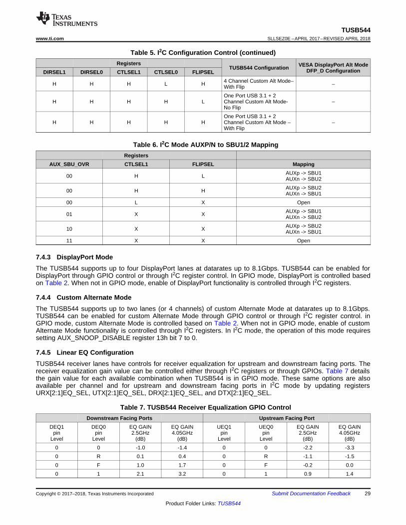
7.4.2 Device Configuration in I2C ModeThe TUSB544 is in I2C mode when I2C_EN is equal to “1”. The same configurations defined in GPIO mode arealso available in I2C mode. The TUSB544’s USB3.1, DisplayPort, and custom Alternate Mode configuration iscontrolled based on Table 5. The AUXP/N to SBU1/2 mapping control is based on Table 5.
Table 5. I2C Configuration ControlRegisters
TUSB544 Configuration VESA DisplayPort Alt ModeDFP_D ConfigurationDIRSEL1 DIRSEL0 CTLSEL1 CTLSEL0 FLIPSEL
USB + DisplayPort Alternate Mode (Source Side)L L L L L Power Down –L L L L H Power Down –L L L H L One Port USB 3.1 - No Flip –L L L H H One Port USB 3.1 – With Flip –L L H L L 4 Lane DP - No Flip C and EL L H L H 4 Lane DP – With Flip C and E
L L H H L One Port USB 3.1 + 2 LaneDP- No Flip D and F
L L H H H One Port USB 3.1 + 2 LaneDP– With Flip D and F
USB + DisplayPort Alternate Mode (Sink Side)L H L L L Power Down –L H L L H Power Down –L H L H L One Port USB 3.1 - No Flip –L H L H H One Port USB 3.1 – With Flip –L H H L L 4 Lane DP - No Flip C and EL H H L H 4 Lane DP – With Flip C and E
L H H H L One Port USB 3.1 + 2 LaneDP- No Flip D and F
L H H H H One Port USB 3.1 + 2 LaneDP– With Flip D and F
USB + Custom Alternate Mode (Source Side)H L L L L Power Down –H L L L H Power Down –H L L H L One Port USB 3.1 - No Flip –H L L H H One Port USB 3.1 – With Flip –
H L H L L 4 Channel Custom Alt Mode -No Flip –
H L H L H 4 Channel Custom Alt Mode–With Flip –
H L H H LOne Port USB 3.1 + 2Channel Custom Alt Mode-No Flip
–
H L H H HOne Port USB 3.1 + 2Channel Custom Alt Mode –With Flip
–
USB + Custom Alternate Mode (Sink Side)H H L L L Power Down –H H L L H Power Down –H H L H L One Port USB 3.1 - No Flip –H H L H H One Port USB 3.1 – With Flip –
H H H L L 4 Channel Custom Alt Mode -No Flip –
29
TUSB544www.ti.com SLLSEZ0E –APRIL 2017–REVISED APRIL 2018
Product Folder Links: TUSB544
Submit Documentation FeedbackCopyright © 2017–2018, Texas Instruments Incorporated
Table 5. I2C Configuration Control (continued)Registers
TUSB544 Configuration VESA DisplayPort Alt ModeDFP_D ConfigurationDIRSEL1 DIRSEL0 CTLSEL1 CTLSEL0 FLIPSEL
H H H L H 4 Channel Custom Alt Mode–With Flip –
H H H H LOne Port USB 3.1 + 2Channel Custom Alt Mode-No Flip
–
H H H H HOne Port USB 3.1 + 2Channel Custom Alt Mode –With Flip
–
Table 6. I2C Mode AUXP/N to SBU1/2 MappingRegisters
AUX_SBU_OVR CTLSEL1 FLIPSEL Mapping
00 H L AUXp -> SBU1AUXn -> SBU2
00 H H AUXp -> SBU2AUXn -> SBU1
00 L X Open
01 X X AUXp -> SBU1AUXn -> SBU2
10 X X AUXp -> SBU2AUXn -> SBU1
11 X X Open
7.4.3 DisplayPort ModeThe TUSB544 supports up to four DisplayPort lanes at datarates up to 8.1Gbps. TUSB544 can be enabled forDisplayPort through GPIO control or through I2C register control. In GPIO mode, DisplayPort is controlled basedon Table 2. When not in GPIO mode, enable of DisplayPort functionality is controlled through I2C registers.
7.4.4 Custom Alternate ModeThe TUSB544 supports up to two lanes (or 4 channels) of custom Alternate Mode at datarates up to 8.1Gbps.TUSB544 can be enabled for custom Alternate Mode through GPIO control or through I2C register control. inGPIO mode, custom Alternate Mode is controlled based on Table 2. When not in GPIO mode, enable of customAlternate Mode functionality is controlled through I2C registers. In I2C mode, the operation of this mode requiressetting AUX_SNOOP_DISABLE register 13h bit 7 to 0.
7.4.5 Linear EQ ConfigurationTUSB544 receiver lanes have controls for receiver equalization for upstream and downstream facing ports. Thereceiver equalization gain value can be controlled either through I2C registers or through GPIOs. Table 7 detailsthe gain value for each available combination when TUSB544 is in GPIO mode. These same options are alsoavailable per channel and for upstream and downstream facing ports in I2C mode by updating registersURX[2:1]EQ_SEL, UTX[2:1]EQ_SEL, DRX[2:1]EQ_SEL, and DTX[2:1]EQ_SEL.
Table 7. TUSB544 Receiver Equalization GPIO ControlDownstream Facing Ports Upstream Facing Port
DEQ1pin
Level
DEQ0pin
Level
EQ GAIN2.5GHz
(dB)
EQ GAIN4.05GHz
(dB)
UEQ1pin
Level
UEQ0pin
Level
EQ GAIN2.5GHz
(dB)
EQ GAIN4.05GHz
(dB)0 0 -1.0 -1.4 0 0 -2.2 -3.30 R 0.1 0.4 0 R -1.1 -1.50 F 1.0 1.7 0 F -0.2 0.00 1 2.1 3.2 0 1 0.9 1.4
30
TUSB544SLLSEZ0E –APRIL 2017–REVISED APRIL 2018 www.ti.com
Product Folder Links: TUSB544
Submit Documentation Feedback Copyright © 2017–2018, Texas Instruments Incorporated
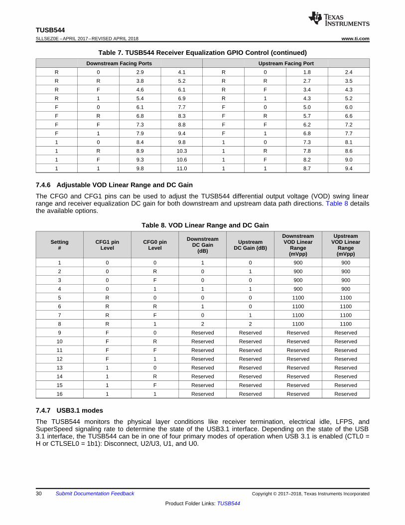
Table 7. TUSB544 Receiver Equalization GPIO Control (continued)Downstream Facing Ports Upstream Facing Port
R 0 2.9 4.1 R 0 1.8 2.4R R 3.8 5.2 R R 2.7 3.5R F 4.6 6.1 R F 3.4 4.3R 1 5.4 6.9 R 1 4.3 5.2F 0 6.1 7.7 F 0 5.0 6.0F R 6.8 8.3 F R 5.7 6.6F F 7.3 8.8 F F 6.2 7.2F 1 7.9 9.4 F 1 6.8 7.71 0 8.4 9.8 1 0 7.3 8.11 R 8.9 10.3 1 R 7.8 8.61 F 9.3 10.6 1 F 8.2 9.01 1 9.8 11.0 1 1 8.7 9.4
7.4.6 Adjustable VOD Linear Range and DC GainThe CFG0 and CFG1 pins can be used to adjust the TUSB544 differential output voltage (VOD) swing linearrange and receiver equalization DC gain for both downstream and upstream data path directions. Table 8 detailsthe available options.
Table 8. VOD Linear Range and DC Gain
Setting#
CFG1 pinLevel
CFG0 pinLevel
DownstreamDC Gain
(dB)Upstream
DC Gain (dB)
DownstreamVOD Linear
Range(mVpp)
UpstreamVOD Linear
Range(mVpp)
1 0 0 1 0 900 9002 0 R 0 1 900 9003 0 F 0 0 900 9004 0 1 1 1 900 9005 R 0 0 0 1100 11006 R R 1 0 1100 11007 R F 0 1 1100 11008 R 1 2 2 1100 11009 F 0 Reserved Reserved Reserved Reserved10 F R Reserved Reserved Reserved Reserved11 F F Reserved Reserved Reserved Reserved12 F 1 Reserved Reserved Reserved Reserved13 1 0 Reserved Reserved Reserved Reserved14 1 R Reserved Reserved Reserved Reserved15 1 F Reserved Reserved Reserved Reserved16 1 1 Reserved Reserved Reserved Reserved
7.4.7 USB3.1 modesThe TUSB544 monitors the physical layer conditions like receiver termination, electrical idle, LFPS, andSuperSpeed signaling rate to determine the state of the USB3.1 interface. Depending on the state of the USB3.1 interface, the TUSB544 can be in one of four primary modes of operation when USB 3.1 is enabled (CTL0 =H or CTLSEL0 = 1b1): Disconnect, U2/U3, U1, and U0.
31
TUSB544www.ti.com SLLSEZ0E –APRIL 2017–REVISED APRIL 2018
Product Folder Links: TUSB544
Submit Documentation FeedbackCopyright © 2017–2018, Texas Instruments Incorporated
The Disconnect mode is the state in which TUSB544 has not detected far-end termination on both upstreamfacing port (UFP) or downstream facing port (DFP). The disconnect mode is the lowest power mode of each ofthe four modes. The TUSB544 will remain in this mode until far-end receiver termination has been detected onboth UFP and DFP. The TUSB544 will immediately exit this mode and enter U0 once far-end termination isdetected.
Once in U0 mode, the TUSB544 will redrive all traffic received on UFP and DFP. U0 is the highest power modeof all USB3.1 modes. The TUSB544 will remain in U0 mode until electrical idle occurs on both UFP and DFP.Upon detecting electrical idle, the TUSB544 will immediately transition to U1.
The U1 mode is the intermediate mode between U0 mode and U2/U3 mode. In U1 mode, the TUSB544’s UFPand DFP receiver termination will remain enabled. The UFP and DFP transmitter DC common mode ismaintained. The power consumption in U1 will be similar to power consumption of U0.
Next to the disconnect mode, the U2 and U3 mode is next lowest power state. While in this mode, the TUSB544will periodically perform far-end receiver detection. Anytime the far-end receiver termination is not detected oneither UFP or DFP, the TUSB544 will leave the U2 and U3 mode and transition to the Disconnect mode. It willalso monitor for a valid LFPS. Upon detection of a valid LFPS, the TUSB544 will immediately transition to the U0mode. In U2 and U3 mode, the TUSB544’s receiver terminations will remain enabled but the TX DC commonmode voltage will not be maintained.
When SLP_S0# is asserted low it will disable Receiver Detect functionality. While SLP_S0# is low and TUSB544is in U2 and U3, TUSB544 will disable LOS and LFPS detection circuitry and RX termination for both channelswill remain enabled. This allows even lower TUSB544 power consumption while in the U2 and U3 mode. OnceSLP_S0# is asserted high, the TUSB544 will again start performing far-end receiver detection as well as monitorLFPS so it can know when to exit the U2 and U3 mode.
When SLP_S0# is asserted low and the TUSB544 is in Disconnect mode, the TUSB544 will remain inDisconnect mode and never perform far-end receiver detection. This allows even lower TUSB544 powerconsumption while in the Disconnect mode. Once SLP_S0# is asserted high, the TUSB544 will again startperforming far-end receiver detection so it can know when to exit the Disconnect mode.
Td_pg
VCC
Internal
Power
GoodTcfg_su
Tcfg_hd
DISABLED USB3.1-only
FLIP = 0
If ((CTL[1:0] == 2'b00 | CTL[1:0] == 2'b01) & FLIP == 0 )
USB3.1-only no FLIP;
ELSEIF ((CTL[1:0] == 2'b00 | CTL[1:0] == 2'b01) & FLIP == 1 )
USB3.1-only with FLIP;
ELSEIF (CTL[1:0] == 2'b10 & FLIP == 0)
4-Lane DP no FLIP;
ELSEIF (CTL[1:0] == 2'b10 & FLIP == 1)
4-Lane DP with FLIP;
ELSEIF (CTL[1:0] == 2'b11 & FLIP == 0)
2-Lane DP USB3.1 no FLIP;
ELSE
2-lane DP USB3.1 with FLIP;
;
CTL[1:0] pins
FLIP pin
CFG pins
TUSB544
In GPIO mode
DISABLED USB3.1-only
FLIP = 0
TUSB544
In I2C mode
Mode of operation
determined by value of
FLIPSEL bit and CTLSEL[1:0]
bits at offset 0x0A. Default
is USB3.1-only no Flip.
Tctl_db
VCC (min)
32
TUSB544SLLSEZ0E –APRIL 2017–REVISED APRIL 2018 www.ti.com
Product Folder Links: TUSB544
Submit Documentation Feedback Copyright © 2017–2018, Texas Instruments Incorporated
7.4.8 Operation Timing – Power Up
Figure 21. Power-Up Timing
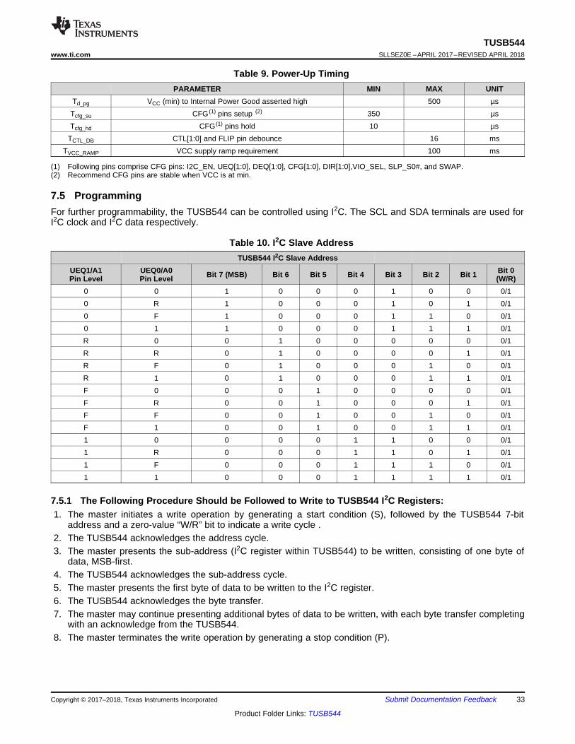
33
TUSB544www.ti.com SLLSEZ0E –APRIL 2017–REVISED APRIL 2018
Product Folder Links: TUSB544
Submit Documentation FeedbackCopyright © 2017–2018, Texas Instruments Incorporated
(1) Following pins comprise CFG pins: I2C_EN, UEQ[1:0], DEQ[1:0], CFG[1:0], DIR[1:0],VIO_SEL, SLP_S0#, and SWAP.(2) Recommend CFG pins are stable when VCC is at min.
Table 9. Power-Up TimingPARAMETER MIN MAX UNIT
Td_pg VCC (min) to Internal Power Good asserted high 500 µsTcfg_su CFG (1) pins setup (2) 350 µsTcfg_hd CFG (1) pins hold 10 µs
TCTL_DB CTL[1:0] and FLIP pin debounce 16 msTVCC_RAMP VCC supply ramp requirement 100 ms
7.5 ProgrammingFor further programmability, the TUSB544 can be controlled using I2C. The SCL and SDA terminals are used forI2C clock and I2C data respectively.
Table 10. I2C Slave AddressTUSB544 I2C Slave Address
UEQ1/A1Pin Level
UEQ0/A0Pin Level Bit 7 (MSB) Bit 6 Bit 5 Bit 4 Bit 3 Bit 2 Bit 1 Bit 0
(W/R)0 0 1 0 0 0 1 0 0 0/10 R 1 0 0 0 1 0 1 0/10 F 1 0 0 0 1 1 0 0/10 1 1 0 0 0 1 1 1 0/1R 0 0 1 0 0 0 0 0 0/1R R 0 1 0 0 0 0 1 0/1R F 0 1 0 0 0 1 0 0/1R 1 0 1 0 0 0 1 1 0/1F 0 0 0 1 0 0 0 0 0/1F R 0 0 1 0 0 0 1 0/1F F 0 0 1 0 0 1 0 0/1F 1 0 0 1 0 0 1 1 0/11 0 0 0 0 1 1 0 0 0/11 R 0 0 0 1 1 0 1 0/11 F 0 0 0 1 1 1 0 0/11 1 0 0 0 1 1 1 1 0/1
7.5.1 The Following Procedure Should be Followed to Write to TUSB544 I2C Registers:1. The master initiates a write operation by generating a start condition (S), followed by the TUSB544 7-bit
address and a zero-value “W/R” bit to indicate a write cycle .2. The TUSB544 acknowledges the address cycle.3. The master presents the sub-address (I2C register within TUSB544) to be written, consisting of one byte of
data, MSB-first.4. The TUSB544 acknowledges the sub-address cycle.5. The master presents the first byte of data to be written to the I2C register.6. The TUSB544 acknowledges the byte transfer.7. The master may continue presenting additional bytes of data to be written, with each byte transfer completing
with an acknowledge from the TUSB544.8. The master terminates the write operation by generating a stop condition (P).
34
TUSB544SLLSEZ0E –APRIL 2017–REVISED APRIL 2018 www.ti.com
Product Folder Links: TUSB544
Submit Documentation Feedback Copyright © 2017–2018, Texas Instruments Incorporated
7.5.2 The Following Procedure Should be Followed to Read the TUSB544 I2C Registers:1. The master initiates a read operation by generating a start condition (S), followed by the TUSB544 7-bit
address and a one-value “W/R” bit to indicate a read cycle2. The TUSB544 acknowledges the address cycle.3. The TUSB544 transmit the contents of the memory registers MSB-first starting at register 00h or last read
sub-address+1. If a write to the TUSB544 I2C register occurred prior to the read, then the TUSB544 shallstart at the sub-address specified in the write.
4. The TUSB544 shall wait for either an acknowledge (ACK) or a not-acknowledge (NACK) from the masterafter each byte transfer; the I2C master acknowledges reception of each data byte transfer.
5. If an ACK is received, the TUSB544 transmits the next byte of data.6. The master terminates the read operation by generating a stop condition (P).
7.5.3 The Following Procedure Should be Followed for Setting a Starting Sub-Address for I2C Reads:1. The master initiates a write operation by generating a start condition (S), followed by the TUSB544 7-bit
address and a zero-value “W/R” bit to indicate a write cycle.2. The TUSB544 acknowledges the address cycle.3. The master presents the sub-address (I2C register within TUSB544) to be written, consisting of one byte of
data, MSB-first.4. The TUSB544 acknowledges the sub-address cycle.5. The master terminates the write operation by generating a stop condition (P).
NOTEIf no sub-addressing is included for the read procedure, and reads start at register offset00h and continue byte by byte through the registers until the I2C master terminates theread operation. If a I2C address write occurred prior to the read, then the reads start at thesub-address specified by the address write.
7.6 Register Maps
7.6.1 TUSB544 RegistersTable 11 lists the memory-mapped registers for the TUSB544. All register offset addresses not listed in Table 11should be considered as reserved locations and the register contents should not be modified.
Table 11. TUSB544 RegistersOffset Acronym Register Name Section
Ah GENERAL_4 General Registers 4 GoBh GENERAL_5 General Register 5 GoCh GENERAL_6 General Register 6 Go10h DISPLAYPORT_1 DisplayPort Control/Status Registers 1 Go11h DISPLAYPORT_2 DisplayPort Control/Status Registers 2 Go12h DISPLAYPORT__3 DisplayPort Control/Status Registers 3 Go13h DISPLAYPORT_4 DisplayPort Control/Status Registers 4 Go1Bh DISPLAYPORT_5 DisplayPort Control/Status Registers 5 Go20h USB3.1_1 USB3.1 Control/Status Registers 1 Go21h USB3.1_2 USB3.1 Control/Status Registers 2 Go22h USB3.1_3 USB3.1 Control/Status Registers 3 Go23h USB3.1_4 USB3.1 Control/Status Registers 4 Go
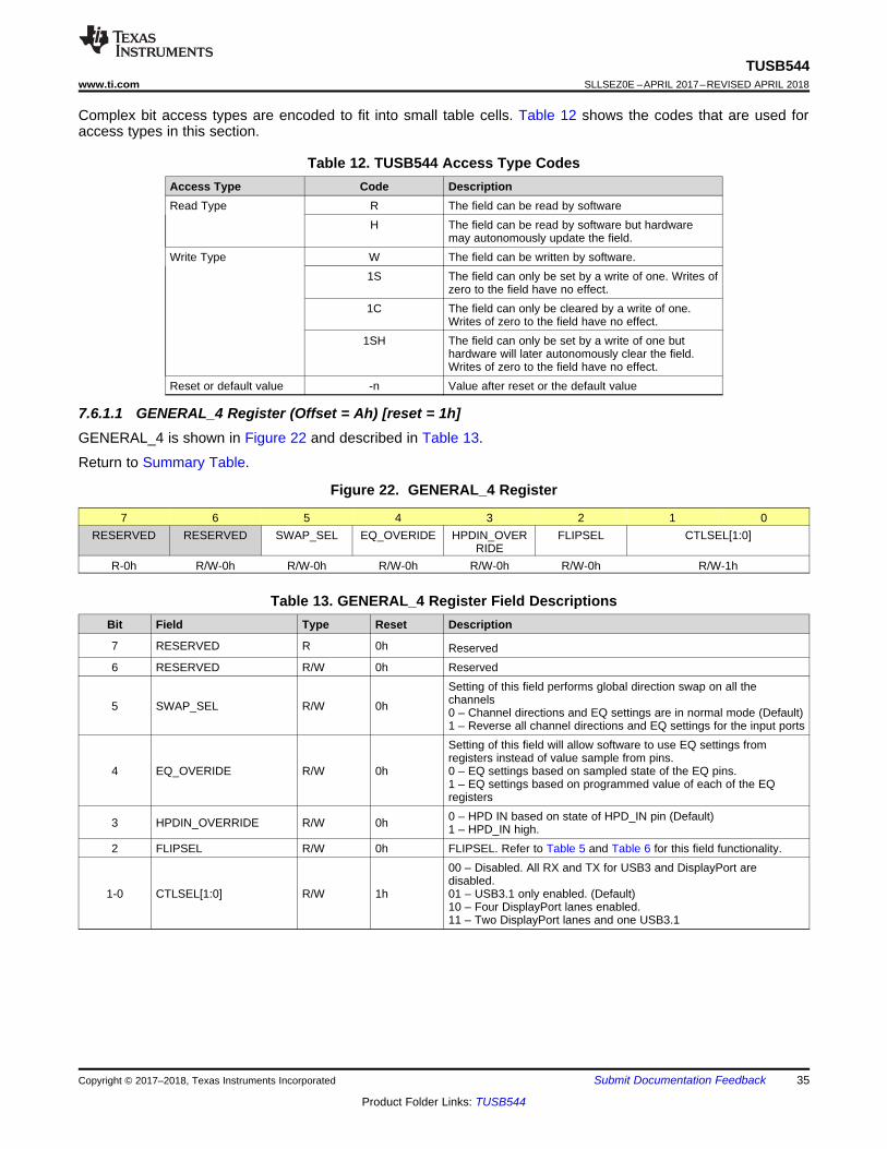
35
TUSB544www.ti.com SLLSEZ0E –APRIL 2017–REVISED APRIL 2018
Product Folder Links: TUSB544
Submit Documentation FeedbackCopyright © 2017–2018, Texas Instruments Incorporated
Complex bit access types are encoded to fit into small table cells. Table 12 shows the codes that are used foraccess types in this section.
Table 12. TUSB544 Access Type CodesAccess Type Code DescriptionRead Type R The field can be read by software
H The field can be read by software but hardwaremay autonomously update the field.
Write Type W The field can be written by software.1S The field can only be set by a write of one. Writes of
zero to the field have no effect.1C The field can only be cleared by a write of one.
Writes of zero to the field have no effect.1SH The field can only be set by a write of one but
hardware will later autonomously clear the field.Writes of zero to the field have no effect.
Reset or default value -n Value after reset or the default value
7.6.1.1 GENERAL_4 Register (Offset = Ah) [reset = 1h]GENERAL_4 is shown in Figure 22 and described in Table 13.
Return to Summary Table.
Figure 22. GENERAL_4 Register
7 6 5 4 3 2 1 0RESERVED RESERVED SWAP_SEL EQ_OVERIDE HPDIN_OVER
RIDEFLIPSEL CTLSEL[1:0]
R-0h R/W-0h R/W-0h R/W-0h R/W-0h R/W-0h R/W-1h
Table 13. GENERAL_4 Register Field DescriptionsBit Field Type Reset Description
7 RESERVED R 0h Reserved6 RESERVED R/W 0h Reserved
5 SWAP_SEL R/W 0h
Setting of this field performs global direction swap on all thechannels0 – Channel directions and EQ settings are in normal mode (Default)1 – Reverse all channel directions and EQ settings for the input ports
4 EQ_OVERIDE R/W 0h
Setting of this field will allow software to use EQ settings fromregisters instead of value sample from pins.0 – EQ settings based on sampled state of the EQ pins.1 – EQ settings based on programmed value of each of the EQregisters
3 HPDIN_OVERRIDE R/W 0h 0 – HPD IN based on state of HPD_IN pin (Default)1 – HPD_IN high.
2 FLIPSEL R/W 0h FLIPSEL. Refer to Table 5 and Table 6 for this field functionality.
1-0 CTLSEL[1:0] R/W 1h
00 – Disabled. All RX and TX for USB3 and DisplayPort aredisabled.01 – USB3.1 only enabled. (Default)10 – Four DisplayPort lanes enabled.11 – Two DisplayPort lanes and one USB3.1
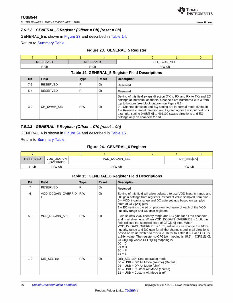
36
TUSB544SLLSEZ0E –APRIL 2017–REVISED APRIL 2018 www.ti.com
Product Folder Links: TUSB544
Submit Documentation Feedback Copyright © 2017–2018, Texas Instruments Incorporated
7.6.1.2 GENERAL_5 Register (Offset = Bh) [reset = 0h]GENERAL_5 is shown in Figure 23 and described in Table 14.
Return to Summary Table.
Figure 23. GENERAL_5 Register
7 6 5 4 3 2 1 0RESERVED RESERVED CH_SWAP_SEL
R-0h R-0h R/W-0h
Table 14. GENERAL_5 Register Field DescriptionsBit Field Type Reset Description
7-6 RESERVED R 0h Reserved
5-4 RESERVED R 0h Reserved
3-0 CH_SWAP_SEL R/W 0h
Setting of this field swaps direction (TX to RX and RX to TX) and EQsettings of individual channels. Channels are numbered 0 to 3 fromtop to bottom (see block diagram on Figure 8.1).0 – Channel direction and EQ setting are in normal mode (Default)1 – Reverse channel direction and EQ setting for the input port. Forexample, setting 0x0B[3:0] to 4b1100 swaps directions and EQsettings only on channels 2 and 3
7.6.1.3 GENERAL_6 Register (Offset = Ch) [reset = 0h]GENERAL_6 is shown in Figure 24 and described in Table 15.
Return to Summary Table.
Figure 24. GENERAL_6 Register
7 6 5 4 3 2 1 0RESERVED VOD_DCGAIN
_OVERRIDEVOD_DCGAIN_SEL DIR_SEL[1:0]
R-0h R/W-0h R/W-0h R/W-0h
Table 15. GENERAL_6 Register Field DescriptionsBit Field Type Reset Description7 RESERVED R 0h Reserved6 VOD_DCGAIN_OVERRID
ER/W 0h Setting of this field will allow software to use VOD linearity range and
DC gain settings from registers instead of value sampled from pins.0 – VOD linearity range and DC gain settings based on sampledstate of CFG[2:1] pins.1 – EQ settings based on programmed value of each of the VODlinearity range and DC gain registers
5-2 VOD_DCGAIN_SEL R/W 0h Field selects VOD linearity range and DC gain for all the channelsand in all directions. When VOD_DCGAIN_OVERRIDE = 1’b0, thisfield reflects the sampled state of CFG[1:0] pins. WhenVOD_DCGAIN_OVERRIDE = 1’b1, software can change the VODlinearity range and DC gain for all the channels and in all directionsbased on value written to this field. Refer to Table 8 8. Each CFG isa 2-bit value. The register-to-CFG1/0 mapping is: [5:2] = CFG1[1:0],CFG0[1:0] where CFGx[1:0] mapping is:00 = 001 = R10 = F11 = 1
1-0 DIR_SEL[1:0] R/W 0h DIR_SEL[1:0]. Sets operation mode00 – USB + DP Alt Mode (source) (Default)01 – USB + DP Alt Mode (sink)10 – USB + Custom Alt Mode (source)11 – USB + Custom Alt Mode (sink)
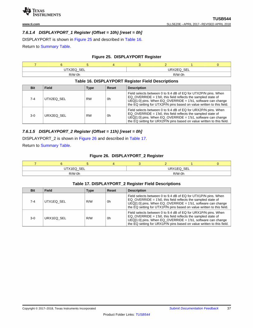
37
TUSB544www.ti.com SLLSEZ0E –APRIL 2017–REVISED APRIL 2018
Product Folder Links: TUSB544
Submit Documentation FeedbackCopyright © 2017–2018, Texas Instruments Incorporated
7.6.1.4 DISPLAYPORT_1 Register (Offset = 10h) [reset = 0h]DISPLAYPORT is shown in Figure 25 and described in Table 16.
Return to Summary Table.
Figure 25. DISPLAYPORT Register
7 6 5 4 3 2 1 0UTX2EQ_SEL URX2EQ_SEL
R/W-0h R/W-0h
Table 16. DISPLAYPORT Register Field DescriptionsBit Field Type Reset Description
7-4 UTX2EQ_SEL RW 0h
Field selects between 0 to 9.4 dB of EQ for UTX2P/N pins. WhenEQ_OVERRIDE = 1’b0, this field reflects the sampled state ofUEQ[1:0] pins. When EQ_OVERRIDE = 1’b1, software can changethe EQ setting for UTX2P/N pins based on value written to this field.
3-0 URX2EQ_SEL RW 0h
Field selects between 0 to 9.4 dB of EQ for URX2P/N pins. WhenEQ_OVERRIDE = 1’b0, this field reflects the sampled state ofUEQ[1:0] pins. When EQ_OVERRIDE = 1’b1, software can changethe EQ setting for URX2P/N pins based on value written to this field.
7.6.1.5 DISPLAYPORT_2 Register (Offset = 11h) [reset = 0h]DISPLAYPORT_2 is shown in Figure 26 and described in Table 17.
Return to Summary Table.
Figure 26. DISPLAYPORT_2 Register
7 6 5 4 3 2 1 0UTX1EQ_SEL URX1EQ_SEL
R/W-0h R/W-0h
Table 17. DISPLAYPORT_2 Register Field DescriptionsBit Field Type Reset Description
7-4 UTX1EQ_SEL R/W 0h
Field selects between 0 to 9.4 dB of EQ for UTX1P/N pins. WhenEQ_OVERRIDE = 1’b0, this field reflects the sampled state ofUEQ[1:0] pins. When EQ_OVERRIDE = 1’b1, software can changethe EQ setting for UTX1P/N pins based on value written to this field.
3-0 URX1EQ_SEL R/W 0h
Field selects between 0 to 9.4 dB of EQ for URX1P/N pins. WhenEQ_OVERRIDE = 1’b0, this field reflects the sampled state ofUEQ[1:0] pins. When EQ_OVERRIDE = 1’b1, software can changethe EQ setting for URX1P/N pins based on value written to this field.
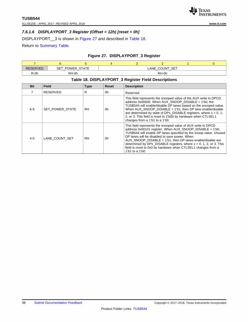
38
TUSB544SLLSEZ0E –APRIL 2017–REVISED APRIL 2018 www.ti.com
Product Folder Links: TUSB544
Submit Documentation Feedback Copyright © 2017–2018, Texas Instruments Incorporated
7.6.1.6 DISPLAYPORT_3 Register (Offset = 12h) [reset = 0h]DISPLAYPORT__3 is shown in Figure 27 and described in Table 18.
Return to Summary Table.
Figure 27. DISPLAYPORT_3 Register
7 6 5 4 3 2 1 0RESERVED SET_POWER_STATE LANE_COUNT_SET
R-0h RH-0h RH-0h
Table 18. DISPLAYPORT_3 Register Field DescriptionsBit Field Type Reset Description
7 RESERVED R 0h Reserved
6-5 SET_POWER_STATE RH 0h
This field represents the snooped value of the AUX write to DPCDaddress 0x00600. When AUX_SNOOP_DISABLE = 1’b0, theTUSB544 will enable/disable DP lanes based on the snooped value.When AUX_SNOOP_DISABLE = 1’b1, then DP lane enable/disableare determined by state of DPx_DISABLE registers, where x = 0, 1,2, or 3. This field is reset to 2’b00 by hardware when CTLSEL1changes from a 1’b1 to a 1’b0.
4-0 LANE_COUNT_SET RH 0h
This field represents the snooped value of AUX write to DPCDaddress 0x00101 register. When AUX_SNOOP_DISABLE = 1’b0,TUSB544 will enable DP lanes specified by the snoop value. UnusedDP lanes will be disabled to save power. WhenAUX_SNOOP_DISABLE = 1’b1, then DP lanes enable/disable aredetermined by DPx_DISABLE registers, where x = 0, 1, 2, or 3. Thisfield is reset to 0x0 by hardware when CTLSEL1 changes from a1’b1 to a 1’b0.
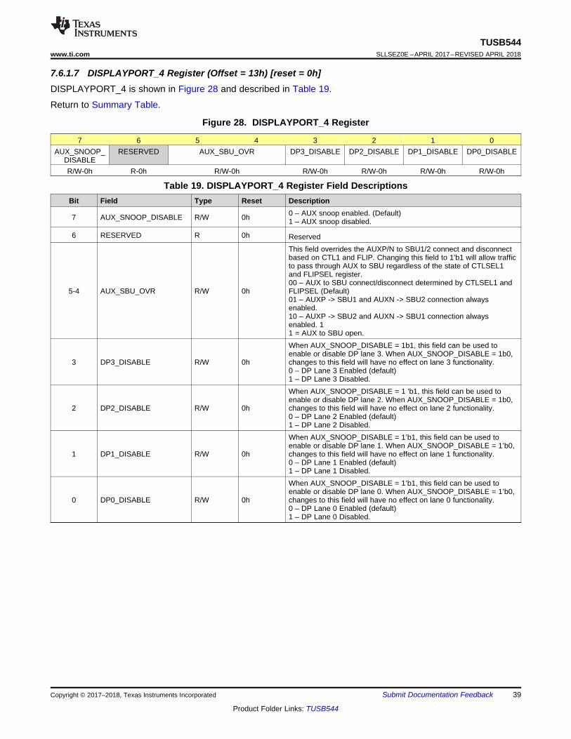
39
TUSB544www.ti.com SLLSEZ0E –APRIL 2017–REVISED APRIL 2018
Product Folder Links: TUSB544
Submit Documentation FeedbackCopyright © 2017–2018, Texas Instruments Incorporated
7.6.1.7 DISPLAYPORT_4 Register (Offset = 13h) [reset = 0h]DISPLAYPORT_4 is shown in Figure 28 and described in Table 19.
Return to Summary Table.
Figure 28. DISPLAYPORT_4 Register
7 6 5 4 3 2 1 0AUX_SNOOP_
DISABLERESERVED AUX_SBU_OVR DP3_DISABLE DP2_DISABLE DP1_DISABLE DP0_DISABLE
R/W-0h R-0h R/W-0h R/W-0h R/W-0h R/W-0h R/W-0h
Table 19. DISPLAYPORT_4 Register Field DescriptionsBit Field Type Reset Description
7 AUX_SNOOP_DISABLE R/W 0h 0 – AUX snoop enabled. (Default)1 – AUX snoop disabled.
6 RESERVED R 0h Reserved
5-4 AUX_SBU_OVR R/W 0h
This field overrides the AUXP/N to SBU1/2 connect and disconnectbased on CTL1 and FLIP. Changing this field to 1’b1 will allow trafficto pass through AUX to SBU regardless of the state of CTLSEL1and FLIPSEL register.00 – AUX to SBU connect/disconnect determined by CTLSEL1 andFLIPSEL (Default)01 – AUXP -> SBU1 and AUXN -> SBU2 connection alwaysenabled.10 – AUXP -> SBU2 and AUXN -> SBU1 connection alwaysenabled. 11 = AUX to SBU open.
3 DP3_DISABLE R/W 0h
When AUX_SNOOP_DISABLE = 1b1, this field can be used toenable or disable DP lane 3. When AUX_SNOOP_DISABLE = 1b0,changes to this field will have no effect on lane 3 functionality.0 – DP Lane 3 Enabled (default)1 – DP Lane 3 Disabled.
2 DP2_DISABLE R/W 0h
When AUX_SNOOP_DISABLE = 1 'b1, this field can be used toenable or disable DP lane 2. When AUX_SNOOP_DISABLE = 1b0,changes to this field will have no effect on lane 2 functionality.0 – DP Lane 2 Enabled (default)1 – DP Lane 2 Disabled.
1 DP1_DISABLE R/W 0h
When AUX_SNOOP_DISABLE = 1’b1, this field can be used toenable or disable DP lane 1. When AUX_SNOOP_DISABLE = 1’b0,changes to this field will have no effect on lane 1 functionality.0 – DP Lane 1 Enabled (default)1 – DP Lane 1 Disabled.
0 DP0_DISABLE R/W 0h
When AUX_SNOOP_DISABLE = 1’b1, this field can be used toenable or disable DP lane 0. When AUX_SNOOP_DISABLE = 1’b0,changes to this field will have no effect on lane 0 functionality.0 – DP Lane 0 Enabled (default)1 – DP Lane 0 Disabled.

40
TUSB544SLLSEZ0E –APRIL 2017–REVISED APRIL 2018 www.ti.com
Product Folder Links: TUSB544
Submit Documentation Feedback Copyright © 2017–2018, Texas Instruments Incorporated
7.6.1.8 DISPLAYPORT_5 Register (Offset = 1Bh) [reset = 0h]DISPLAYPORT_5 is shown in Figure 29 and described in Table 20.
Return to Summary Table.
Figure 29. DISPLAYPORT_5 Register
7 6 5 4 3 2 1 0I2C_RST DPCD_RST RESERVED
R/WSH-0h R/WSH-0h R-00h
Table 20. DISPLAYPORT_5 Register Field DescriptionsBit Field Type Reset Description7 I2C_RST R/WSH 0h Resets I2C registers to default values. This field is self- clearing.6 DPCD_RST R/WSH 0h Resets DPCD registers to default values. This field is self- clearing.
5:0 Reserved R 00h Reserved
7.6.1.9 USB3.1_1 Register (Offset = 20h) [reset = 0h]USB3.1 is shown in Figure 30 and described in Table 21.
Return to Summary Table.
Figure 30. USB3.1 Register
7 6 5 4 3 2 1 0DTX2EQ_SEL DRX2EQ_SEL
R/W-0h R/W-0h
Table 21. USB3.1 Register Field DescriptionsBit Field Type Reset Description
7-4 DTX2EQ_SEL R/W 0hField selects between 0 to 11 dB of EQ for DTX2P/N pins. WhenEQ_OVERRIDE = 1’b0, this field reflects the sampled state ofDEQ[1:0] pins. When EQ_OVERRIDE = 1’b1, software can changethe EQ setting for DTX2P/N pins based on value written to this field.
3-0 DRX2EQ_SEL R/W 0hField selects between 0 to 11 dB of EQ for DRX2P/N pins. WhenEQ_OVERRIDE = 1’b0, this field reflects the sampled state ofDEQ[1:0] pins. When EQ_OVERRIDE = 1’b1, software can changethe EQ setting for DRX2P/N pins based on value written to this field.
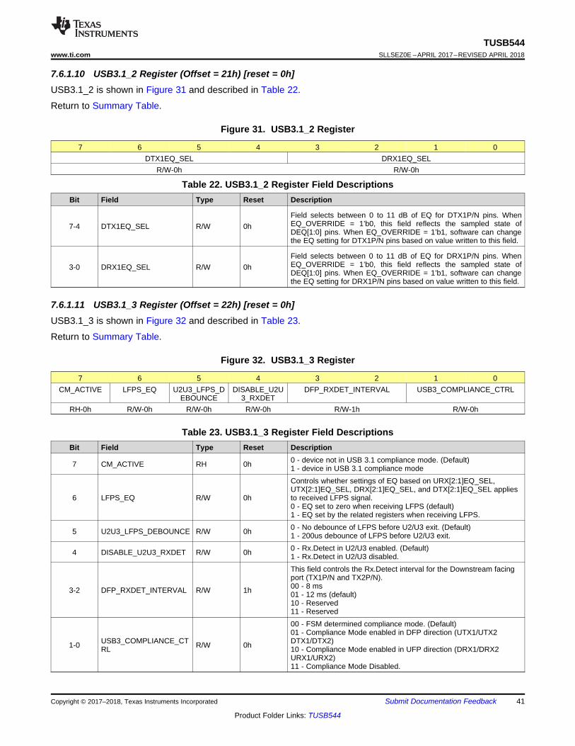
41
TUSB544www.ti.com SLLSEZ0E –APRIL 2017–REVISED APRIL 2018
Product Folder Links: TUSB544
Submit Documentation FeedbackCopyright © 2017–2018, Texas Instruments Incorporated
7.6.1.10 USB3.1_2 Register (Offset = 21h) [reset = 0h]USB3.1_2 is shown in Figure 31 and described in Table 22.
Return to Summary Table.
Figure 31. USB3.1_2 Register
7 6 5 4 3 2 1 0DTX1EQ_SEL DRX1EQ_SEL
R/W-0h R/W-0h
Table 22. USB3.1_2 Register Field DescriptionsBit Field Type Reset Description
7-4 DTX1EQ_SEL R/W 0hField selects between 0 to 11 dB of EQ for DTX1P/N pins. WhenEQ_OVERRIDE = 1’b0, this field reflects the sampled state ofDEQ[1:0] pins. When EQ_OVERRIDE = 1’b1, software can changethe EQ setting for DTX1P/N pins based on value written to this field.
3-0 DRX1EQ_SEL R/W 0hField selects between 0 to 11 dB of EQ for DRX1P/N pins. WhenEQ_OVERRIDE = 1’b0, this field reflects the sampled state ofDEQ[1:0] pins. When EQ_OVERRIDE = 1’b1, software can changethe EQ setting for DRX1P/N pins based on value written to this field.
7.6.1.11 USB3.1_3 Register (Offset = 22h) [reset = 0h]USB3.1_3 is shown in Figure 32 and described in Table 23.
Return to Summary Table.
Figure 32. USB3.1_3 Register
7 6 5 4 3 2 1 0CM_ACTIVE LFPS_EQ U2U3_LFPS_D
EBOUNCEDISABLE_U2U
3_RXDETDFP_RXDET_INTERVAL USB3_COMPLIANCE_CTRL
RH-0h R/W-0h R/W-0h R/W-0h R/W-1h R/W-0h
Table 23. USB3.1_3 Register Field DescriptionsBit Field Type Reset Description
7 CM_ACTIVE RH 0h 0 - device not in USB 3.1 compliance mode. (Default)1 - device in USB 3.1 compliance mode
6 LFPS_EQ R/W 0h
Controls whether settings of EQ based on URX[2:1]EQ_SEL,UTX[2:1]EQ_SEL, DRX[2:1]EQ_SEL, and DTX[2:1]EQ_SEL appliesto received LFPS signal.0 - EQ set to zero when receiving LFPS (default)1 - EQ set by the related registers when receiving LFPS.
5 U2U3_LFPS_DEBOUNCE R/W 0h 0 - No debounce of LFPS before U2/U3 exit. (Default)1 - 200us debounce of LFPS before U2/U3 exit.
4 DISABLE_U2U3_RXDET R/W 0h 0 - Rx.Detect in U2/U3 enabled. (Default)1 - Rx.Detect in U2/U3 disabled.
3-2 DFP_RXDET_INTERVAL R/W 1h
This field controls the Rx.Detect interval for the Downstream facingport (TX1P/N and TX2P/N).00 - 8 ms01 - 12 ms (default)10 - Reserved11 - Reserved
1-0 USB3_COMPLIANCE_CTRL R/W 0h
00 - FSM determined compliance mode. (Default)01 - Compliance Mode enabled in DFP direction (UTX1/UTX2DTX1/DTX2)10 - Compliance Mode enabled in UFP direction (DRX1/DRX2URX1/URX2)11 - Compliance Mode Disabled.
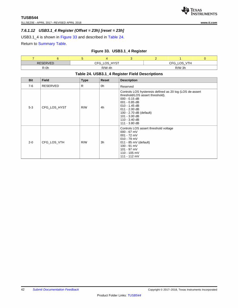
42
TUSB544SLLSEZ0E –APRIL 2017–REVISED APRIL 2018 www.ti.com
Product Folder Links: TUSB544
Submit Documentation Feedback Copyright © 2017–2018, Texas Instruments Incorporated
7.6.1.12 USB3.1_4 Register (Offset = 23h) [reset = 23h]USB3.1_4 is shown in Figure 33 and described in Table 24.
Return to Summary Table.
Figure 33. USB3.1_4 Register
7 6 5 4 3 2 1 0RESERVED CFG_LOS_HYST CFG_LOS_VTH
R-0h R/W-4h R/W-3h
Table 24. USB3.1_4 Register Field DescriptionsBit Field Type Reset Description
7-6 RESERVED R 0h Reserved
5-3 CFG_LOS_HYST R/W 4h
Controls LOS hysteresis defined as 20 log (LOS de-assertthreshold/LOS assert threshold).000 - 0.15 dB001 - 0.85 dB010 - 1.45 dB011 - 2.00 dB100 - 2.70 dB (default)101 - 3.00 dB110 - 3.40 dB111 - 3.80 dB
2-0 CFG_LOS_VTH R/W 3h
Controls LOS assert threshold voltage000 - 67 mV001 - 72 mV010 - 79 mV011 - 85 mV (default)100 - 91 mV101 - 97 mV110 - 105 mV111 - 112 mV
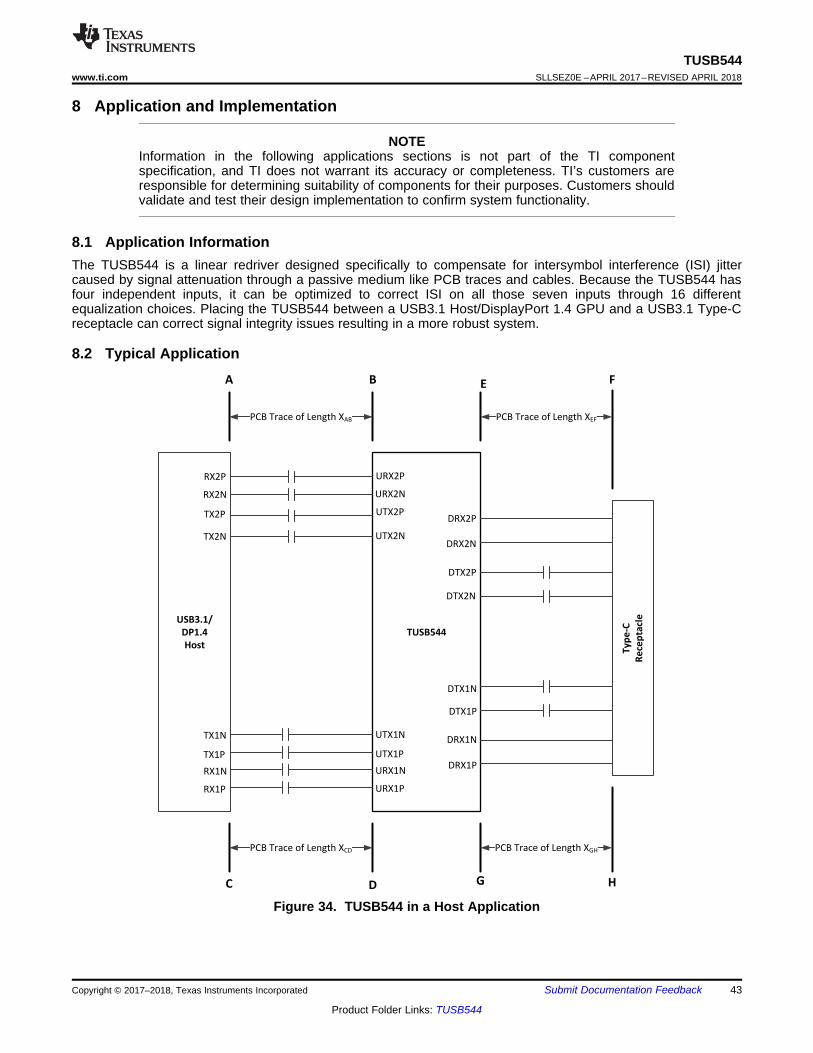
USB3.1/
DP1.4
Host
TUSB544Type-C
Receptacle
UTX1N
UTX1P
URX1N
URX1P
DTX1N
DTX1P
DTX2P
DTX2N
DRX1P
DRX1N
DRX2P
DRX2N
URX2P
URX2N
UTX2P
UTX2N
TX1N
TX1P
RX1N
RX1P
RX2P
RX2N
TX2P
TX2N
A B
C
F
D
E
G H
PCB Trace of Length XAB PCB Trace of Length XEF
PCB Trace of Length XGHPCB Trace of Length XCD
43
TUSB544www.ti.com SLLSEZ0E –APRIL 2017–REVISED APRIL 2018
Product Folder Links: TUSB544
Submit Documentation FeedbackCopyright © 2017–2018, Texas Instruments Incorporated
8 Application and Implementation
NOTEInformation in the following applications sections is not part of the TI componentspecification, and TI does not warrant its accuracy or completeness. TI’s customers areresponsible for determining suitability of components for their purposes. Customers shouldvalidate and test their design implementation to confirm system functionality.
8.1 Application InformationThe TUSB544 is a linear redriver designed specifically to compensate for intersymbol interference (ISI) jittercaused by signal attenuation through a passive medium like PCB traces and cables. Because the TUSB544 hasfour independent inputs, it can be optimized to correct ISI on all those seven inputs through 16 differentequalization choices. Placing the TUSB544 between a USB3.1 Host/DisplayPort 1.4 GPU and a USB3.1 Type-Creceptacle can correct signal integrity issues resulting in a more robust system.
8.2 Typical Application
Figure 34. TUSB544 in a Host Application
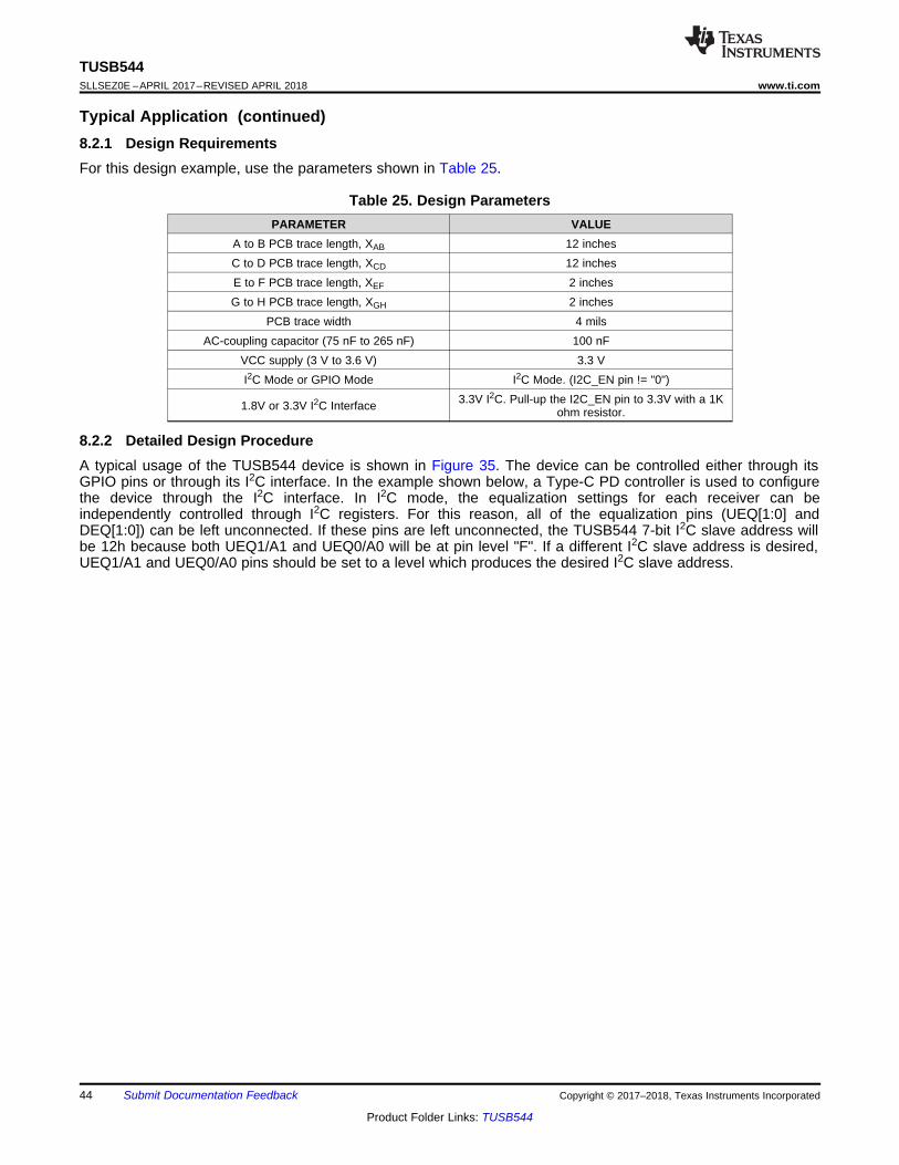
44
TUSB544SLLSEZ0E –APRIL 2017–REVISED APRIL 2018 www.ti.com
Product Folder Links: TUSB544
Submit Documentation Feedback Copyright © 2017–2018, Texas Instruments Incorporated
Typical Application (continued)8.2.1 Design RequirementsFor this design example, use the parameters shown in Table 25.
Table 25. Design ParametersPARAMETER VALUE
A to B PCB trace length, XAB 12 inchesC to D PCB trace length, XCD 12 inchesE to F PCB trace length, XEF 2 inchesG to H PCB trace length, XGH 2 inches
PCB trace width 4 milsAC-coupling capacitor (75 nF to 265 nF) 100 nF
VCC supply (3 V to 3.6 V) 3.3 VI2C Mode or GPIO Mode I2C Mode. (I2C_EN pin != "0")
1.8V or 3.3V I2C Interface 3.3V I2C. Pull-up the I2C_EN pin to 3.3V with a 1Kohm resistor.
8.2.2 Detailed Design ProcedureA typical usage of the TUSB544 device is shown in Figure 35. The device can be controlled either through itsGPIO pins or through its I2C interface. In the example shown below, a Type-C PD controller is used to configurethe device through the I2C interface. In I2C mode, the equalization settings for each receiver can beindependently controlled through I2C registers. For this reason, all of the equalization pins (UEQ[1:0] andDEQ[1:0]) can be left unconnected. If these pins are left unconnected, the TUSB544 7-bit I2C slave address willbe 12h because both UEQ1/A1 and UEQ0/A0 will be at pin level "F". If a different I2C slave address is desired,UEQ1/A1 and UEQ0/A0 pins should be set to a level which produces the desired I2C slave address.
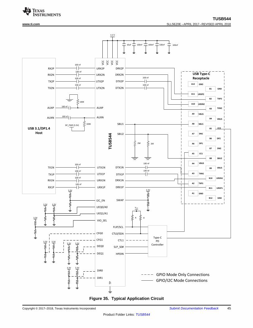
A11
A10
A9
A8
A7
A6
A5
A4
A3
A2
A1
A12
B2
B3
B4
B5
B6
B7
B8
B9
B10
B11
B12
B1 GND
GND
GND
GND
TXP2
TXN2
VBUS
VBUS
VBUS
VBUS
URXP2
URXN2
SBU1
DN1
DP1
CC1
TXN1
TXP1
URXP1
URXN1
SBU2
CC2
DP2
DN2
DRX2P
DRX2N
DTX2P
DTX2N
DTX1N
DTX1P
DRX1N
DRX1P
SBU1
SBU2
AUXP
AUXN
TU
SB
54
4AUXP
AUXN
DP_PWR (3.3V)100K
100K
100 nF
100 nF
100 nF
100 nF
100 nF
100 nF
100 nF
100 nF
100 nF
100 nF
100 nF
100 nF
100 nF
100 nF
USB 3.1/DP1.4
Host
USB Type-C
Receptacle
URX2P
URX2N
UTX2P
UTX2N
UTX1N
UTX1P
URX1N
URX1P
RX2P
RX2N
TX2P
TX2N
TX1N
TX1P
RX1N
RX1P
VC
C
100nF10uF 100nF 100nF 100nF
VC
C
VC
C
VC
C
2M 2M
Type-C
PD
Controller
R
3.3V
3.3V 3.3V
3.3V3.3V 3.3V
R
VI2C
TP
SWAP
3.3V
3.3V
I2C_EN
UEQ0/A0
UEQ1/A1
HPDIN
CFG0
CFG1
DEQ0
DEQ1
SLP_S0#
FLIP/SCL
CTL0/SDA
CTL1
VIO_SEL
GPIO Mode Only Connections
3.3 V
3.3V 3.3V
DIR0
DIR1GPIO/I2C Mode Connections
3.3V
45
TUSB544www.ti.com SLLSEZ0E –APRIL 2017–REVISED APRIL 2018
Product Folder Links: TUSB544
Submit Documentation FeedbackCopyright © 2017–2018, Texas Instruments Incorporated
Figure 35. Typical Application Circuit
Frequency (GHz)
Inse
rtio
n Lo
ss (
dB)
0 2 4 6 8 10 12 14 16-60
-55
-50
-45
-40
-35
-30
-25
-20
-15
-10
-5
0
D009
Length=12in, Width=6milLength=16in, Width=6milLength=20in, Width=6milLength=24in, Width=6milLength=4in, Width=4milLength=8in, Width=10milLength=8in, Width=6mil
46
TUSB544SLLSEZ0E –APRIL 2017–REVISED APRIL 2018 www.ti.com
Product Folder Links: TUSB544
Submit Documentation Feedback Copyright © 2017–2018, Texas Instruments Incorporated
8.2.3 Application Curve
Figure 36. Insertion Loss of FR4 PCB Traces
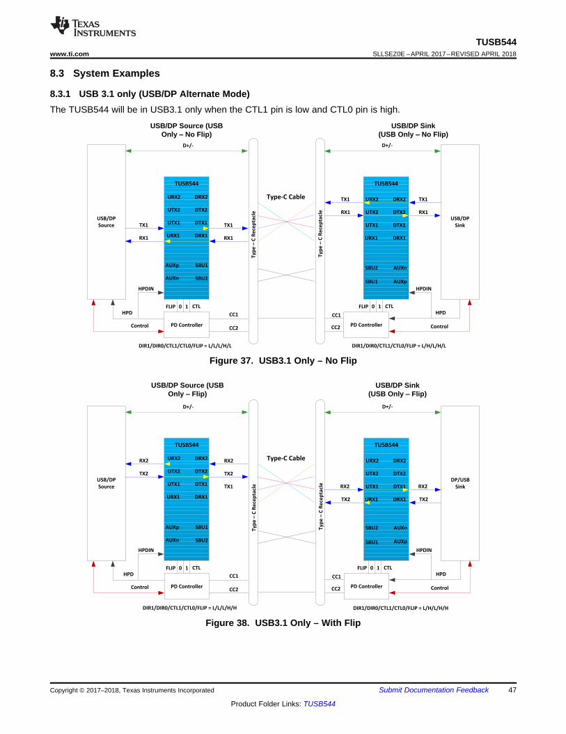
Ty
pe
t C
Re
cep
tacl
e
Ty
pe
t C
Re
cep
tacl
e
USB/DP
Source
TUSB544
SBU1
SBU2
DTX1
DTX2
DRX1
DRX2
PD Controller
CC1
CC2Control
HPDCTLFLIP 0 1
DP/USB
Sink
PD Controller
D+/-
HPD
Control
CTLFLIP 0 1
TX2
RX2
D+/-
CC1
CC2
TUSB544
TX2
RX2UTX1
UTX2
URX1
URX2
DTX1
DTX2
DRX1
DRX2
UTX1
UTX2
URX1
URX2
TX1
TX2
RX2
DIR1/DIR0/CTL1/CTL0/FLIP = L/L/L/H/H
USB/DP Source (USB Only ± Flip)
USB/DP Sink (USB Only ± Flip)
DIR1/DIR0/CTL1/CTL0/FLIP = L/H/L/H/H
TX2
RX2
AUXp
AUXn
Type-C Cable
HPDIN HPDIN
SBU2
SBU1
AUXn
AUXp
Ty
pe
t C
Re
cep
tacl
e
Ty
pe
t C
Re
cep
tacl
e
USB/DP
Source
TUSB544
SBU1
SBU2
DTX1
DTX2
DRX1
DRX2
PD Controller
CC1
CC2Control
HPDCTLFLIP 0 1
USB/DP
Sink
PD Controller
D+/-
HPD
Control
CTLFLIP 0 1
TX1
RX1
D+/-
CC1
CC2
TUSB544
TX1
RX1
UTX1
UTX2
URX1
URX2
DTX1
DTX2
DRX1
DRX2
UTX1
UTX2
URX1
URX2
TX1
RX1
DIR1/DIR0/CTL1/CTL0/FLIP = L/L/L/H/L
USB/DP Source (USB Only ± No Flip)
USB/DP Sink (USB Only ± No Flip)
DIR1/DIR0/CTL1/CTL0/FLIP = L/H/L/H/L
TX1
RX1
AUXp
AUXn
Type-C Cable
HPDIN HPDIN
SBU1
SBU2
AUXp
AUXn
47
TUSB544www.ti.com SLLSEZ0E –APRIL 2017–REVISED APRIL 2018
Product Folder Links: TUSB544
Submit Documentation FeedbackCopyright © 2017–2018, Texas Instruments Incorporated
8.3 System Examples
8.3.1 USB 3.1 only (USB/DP Alternate Mode)The TUSB544 will be in USB3.1 only when the CTL1 pin is low and CTL0 pin is high.
Figure 37. USB3.1 Only – No Flip
Figure 38. USB3.1 Only – With Flip
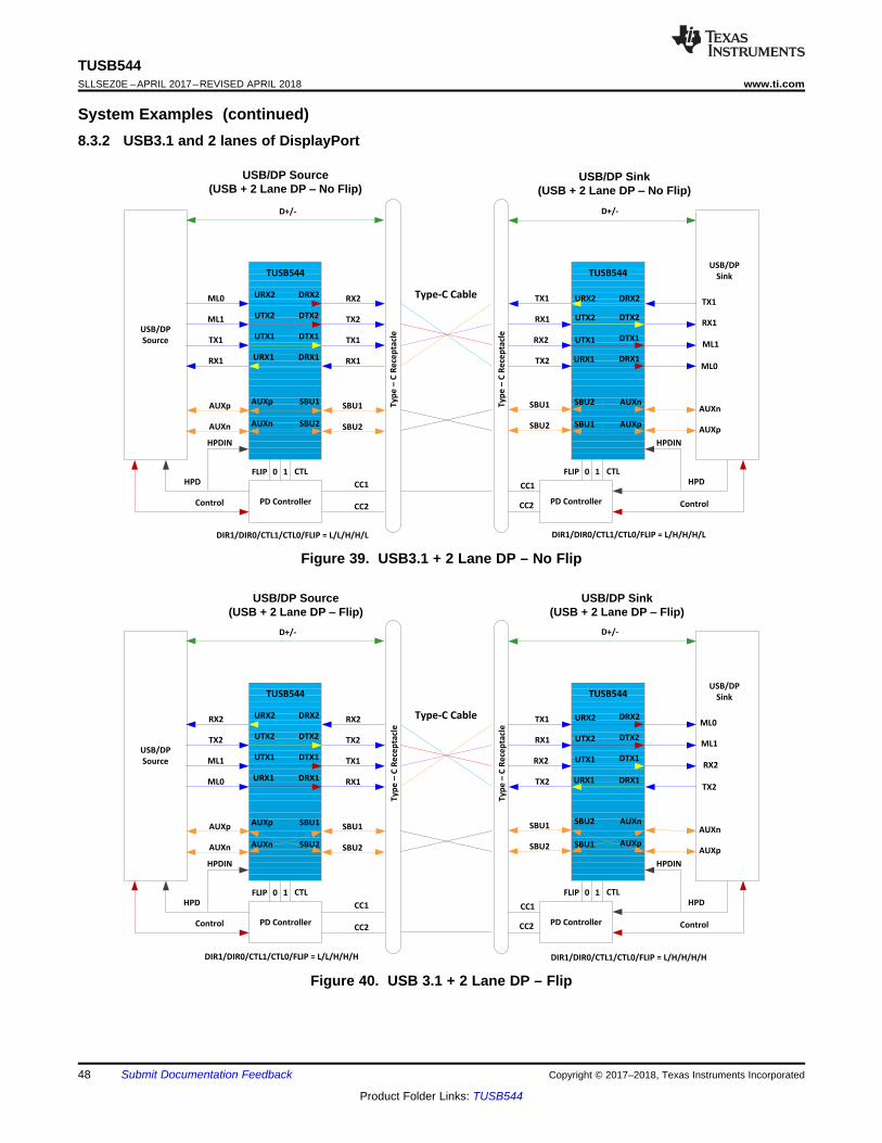
Ty
pe
t C
Re
cep
tacl
e
Ty
pe
t C
Re
cep
tacl
e
DIR1/DIR0/CTL1/CTL0/FLIP = L/L/H/H/H
USB/DP Source (USB + 2 Lane DP ± Flip)
USB/DP Sink (USB + 2 Lane DP ± Flip)
DIR1/DIR0/CTL1/CTL0/FLIP = L/H/H/H/H
USB/DP
Source
TUSB544
SBU1
SBU2
DTX1
DTX2
DRX1
DRX2
PD Controller
CC1
CC2Control
HPDCTLFLIP 0 1
PD Controller
D+/-
HPD
Control
SBU2
SBU1
CTLFLIP 0 1
TX2
TX1
RX2
RX1
D+/-
CC1
CC2
TUSB544
ML0
ML1
UTX1
UTX2
URX1
URX2
DTX1
DTX2
DRX1
DRX2
UTX1
UTX2
URX1
URX2
TX1
TX2
RX1
RX2
ML1
TX2
ML0
RX2
AUXp
AUXn
AUXp
AUXn
SBU1
SBU2
SBU2
SBU1
AUXn
AUXp
Type-C Cable
AUXn
AUXp
TX2
RX2
USB/DP
Sink
HPDIN HPDIN
Ty
pe
t C
Re
cep
tacl
e
Ty
pe
t C
Re
cep
tacl
eUSB/DP
Source
TUSB544
SBU1
SBU2
DTX1
DTX2
DRX1
DRX2
PD Controller
CC1
CC2Control
HPDCTLFLIP 0 1
PD Controller
D+/-
HPD
Control
SBU2
SBU1
CTLFLIP 0 1
TX2
TX1
RX2
RX1
D+/-
CC1
CC2
TUSB544
TX1
RX1
UTX1
UTX2
URX1
URX2
DTX1
DTX2
DRX1
DRX2
UTX1
UTX2
URX1
URX2
TX1
TX2
RX1
RX2
DIR1/DIR0/CTL1/CTL0/FLIP = L/L/H/H/L
USB/DP Source (USB + 2 Lane DP ± No Flip)
USB/DP Sink (USB + 2 Lane DP ± No Flip)
DIR1/DIR0/CTL1/CTL0/FLIP = L/H/H/H/L
TX1
ML1
RX1
ML0
AUXp
AUXn
AUXp
AUXn
SBU1
SBU2 SBU1
SBU2
AUXp
AUXn
Type-C Cable
AUXn
AUXp
ML0
ML1
USB/DP
Sink
HPDIN HPDIN
48
TUSB544SLLSEZ0E –APRIL 2017–REVISED APRIL 2018 www.ti.com
Product Folder Links: TUSB544
Submit Documentation Feedback Copyright © 2017–2018, Texas Instruments Incorporated
System Examples (continued)8.3.2 USB3.1 and 2 lanes of DisplayPort
Figure 39. USB3.1 + 2 Lane DP – No Flip
Figure 40. USB 3.1 + 2 Lane DP – Flip
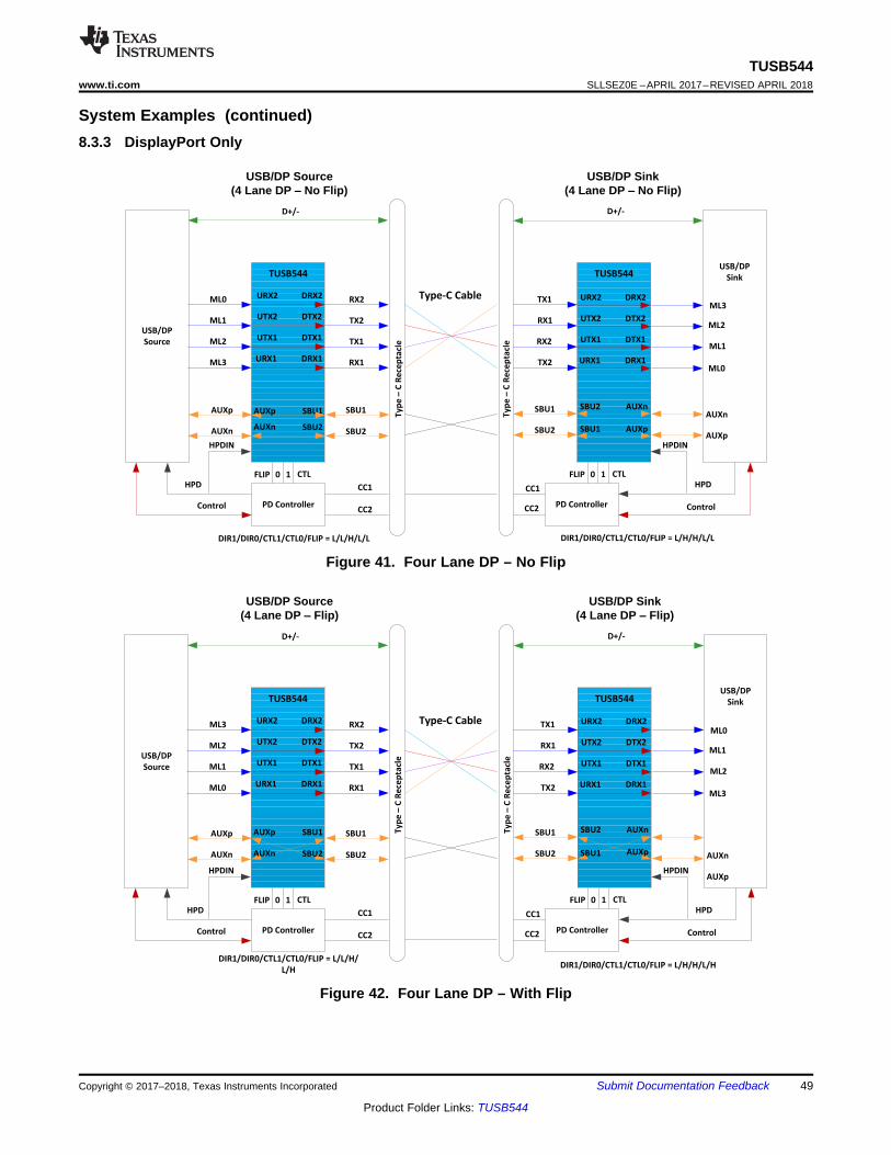
Ty
pe
t C
Re
cep
tacl
e
Ty
pe
t C
Re
cep
tacl
eUSB/DP
Source
TUSB544
SBU1
DTX1
DTX2
DRX1
DRX2
SBU2
PD Controller
CC1
CC2Control
HPDCTLFLIP 0 1
PD Controller
D+/-
HPD
Control
SBU2
SBU1
CTLFLIP 0 1
TX2
TX1
RX2
RX1
D+/-
CC1
CC2
TUSB544
UTX1
UTX2
URX1
URX2
DTX1
DTX2
DRX1
DRX2
UTX1
UTX2
URX1
URX2
TX1
TX2
RX1
RX2
DIR1/DIR0/CTL1/CTL0/FLIP = L/L/H/
L/H
USB/DP Source (4 Lane DP ± Flip)
USB/DP Sink (4 Lane DP ± Flip)
DIR1/DIR0/CTL1/CTL0/FLIP = L/H/H/L/H
ML1
ML2
ML0
ML3
AUXp
AUXn
AUXp
AUXn
SBU1
SBU2
Type-C Cable
AUXn
AUXp
ML3
ML0
ML2
ML1
USB/DP
Sink
HPDIN HPDIN
SBU2
SBU1
AUXn
AUXp
Ty
pe
t C
Re
cep
tacl
e
Ty
pe
t C
Re
cep
tacl
e
USB/DP
Source
TUSB544
SBU1
SBU2
DTX1
DTX2
DRX1
DRX2
PD Controller
CC1
CC2Control
HPDCTLFLIP 0 1
PD Controller
D+/-
HPD
Control
AUXn
AUXpSBU2
SBU1
CTLFLIP 0 1
TX2
TX1
RX2
RX1
D+/-
CC1
CC2
TUSB544
UTX1
UTX2
URX1
URX2
DTX1
DTX2
DRX1
DRX2
UTX1
UTX2
URX1
URX2
TX1
TX2
RX1
RX2
DIR1/DIR0/CTL1/CTL0/FLIP = L/L/H/L/L
USB/DP Source (4 Lane DP ± No Flip)
USB/DP Sink (4 Lane DP ± No Flip)
DIR1/DIR0/CTL1/CTL0/FLIP = L/H/H/L/L
ML2
ML1
ML3
ML0
AUXp
AUXn
AUXp
AUXn
SBU1
SBU2
Type-C Cable
ML0
ML3
ML1
ML2
USB/DP
Sink
HPDIN HPDIN
SBU1
SBU2
AUXp
AUXn
49
TUSB544www.ti.com SLLSEZ0E –APRIL 2017–REVISED APRIL 2018
Product Folder Links: TUSB544
Submit Documentation FeedbackCopyright © 2017–2018, Texas Instruments Incorporated
System Examples (continued)8.3.3 DisplayPort Only
Figure 41. Four Lane DP – No Flip
Figure 42. Four Lane DP – With Flip
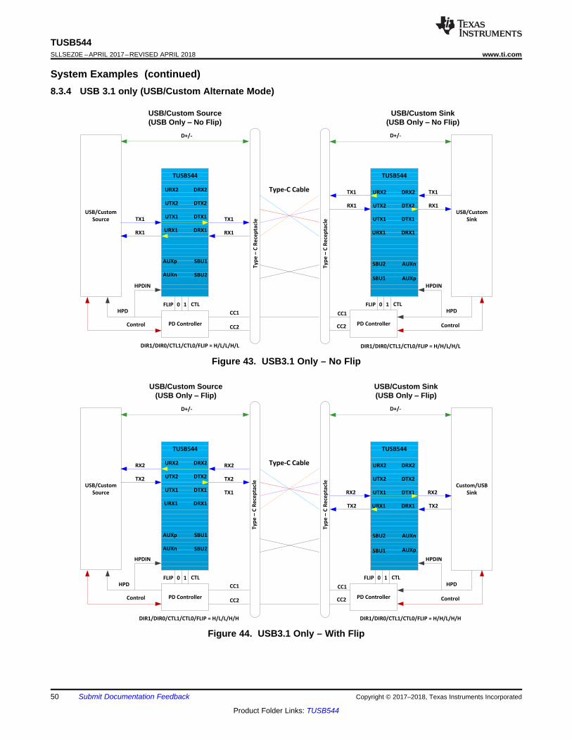
Ty
pe
t C
Re
cep
tacl
e
Ty
pe
t C
Re
cep
tacl
e
USB/Custom
Source
TUSB544
SBU1
SBU2
DTX1
DTX2
DRX1
DRX2
PD Controller
CC1
CC2Control
HPDCTLFLIP 0 1
Custom/USB
Sink
PD Controller
D+/-
HPD
Control
CTLFLIP 0 1
TX2
RX2
D+/-
CC1
CC2
TUSB544
TX2
RX2UTX1
UTX2
URX1
URX2
DTX1
DTX2
DRX1
DRX2
UTX1
UTX2
URX1
URX2
TX1
TX2
RX2
DIR1/DIR0/CTL1/CTL0/FLIP = H/L/L/H/H
USB/Custom Source (USB Only ± Flip)
USB/Custom Sink (USB Only ± Flip)
DIR1/DIR0/CTL1/CTL0/FLIP = H/H/L/H/H
TX2
RX2
AUXp
AUXn
Type-C Cable
HPDIN HPDIN
SBU2
SBU1
AUXn
AUXp
Ty
pe
t C
Re
cep
tacl
e
Ty
pe
t C
Re
cep
tacl
e
USB/Custom
Source
TUSB544
SBU1
SBU2
DTX1
DTX2
DRX1
DRX2
PD Controller
CC1
CC2Control
HPDCTLFLIP 0 1
USB/Custom
Sink
PD Controller
D+/-
HPD
Control
CTLFLIP 0 1
TX1
RX1
D+/-
CC1
CC2
TUSB544
TX1
RX1
UTX1
UTX2
URX1
URX2
DTX1
DTX2
DRX1
DRX2
UTX1
UTX2
URX1
URX2
TX1
RX1
DIR1/DIR0/CTL1/CTL0/FLIP = H/L/L/H/L
USB/Custom Source (USB Only ± No Flip)
USB/Custom Sink (USB Only ± No Flip)
DIR1/DIR0/CTL1/CTL0/FLIP = H/H/L/H/L
TX1
RX1
AUXp
AUXn
Type-C Cable
HPDIN HPDIN
SBU1
SBU2
AUXp
AUXn
50
TUSB544SLLSEZ0E –APRIL 2017–REVISED APRIL 2018 www.ti.com
Product Folder Links: TUSB544
Submit Documentation Feedback Copyright © 2017–2018, Texas Instruments Incorporated
System Examples (continued)8.3.4 USB 3.1 only (USB/Custom Alternate Mode)
Figure 43. USB3.1 Only – No Flip
Figure 44. USB3.1 Only – With Flip
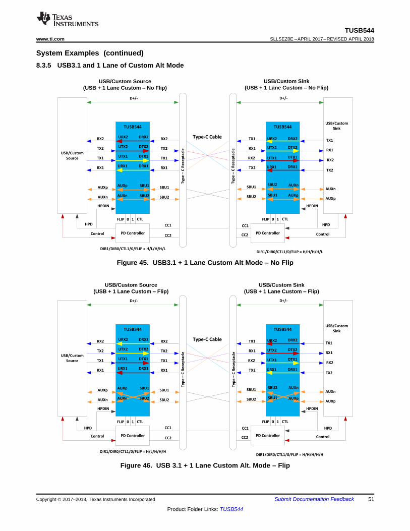
DIR1/DIR0/CTL1/0/FLIP = H/L/H/H/H
USB/Custom Source (USB + 1 Lane Custom ± Flip)
USB/Custom Sink (USB + 1 Lane Custom ± Flip)
DIR1/DIR0/CTL1/0/FLIP = H/H/H/H/H
USB/Custom
Source
TUSB544
DTX1
DTX2
DRX1
DRX2
PD Controller
CC1
CC2Control
CTLFLIP 0 1
PD Controller
D+/-
Control
CTLFLIP 0 1
TX2
TX1
RX2
RX1
D+/-
CC1
CC2
TUSB544
UTX1
UTX2
URX1
URX2
DTX1
DTX2
DRX1
DRX2
UTX1
UTX2
URX1
URX2
TX1
TX2
RX1
RX2
TX1
TX2
RX1
RX2 Type-C Cable
USB/Custom
Sink
TX1
RX1
TX2
RX2
SBU1
SBU2
SBU1AUXp
AUXn
AUXp
AUXn
SBU1
SBU2
AUXn
AUXp
SBU2
SBU1
AUXn
AUXp
HPDIN HPDIN
HPD HPD
Ty
pe
t C
Re
cep
tacl
e
Ty
pe
t C
Re
cep
tacl
e
SBU2
USB/Custom
Source
TUSB544
DTX1
DTX2
DRX1
DRX2
PD Controller
CC1
CC2Control
CTLFLIP 0 1
PD Controller
D+/-
Control
CTLFLIP 0 1
TX2
TX1
RX2
RX1
D+/-
CC1
CC2
TUSB544
TX1
RX1
UTX1
UTX2
URX1
URX2
DTX1
DTX2
DRX1
DRX2
UTX1
UTX2
URX1
URX2
TX1
TX2
RX1
RX2
DIR1/DIR0/CTL1/0/FLIP = H/L/H/H/L
USB/Custom Source (USB + 1 Lane Custom ± No Flip)
USB/Custom Sink (USB + 1 Lane Custom ± No Flip)
DIR1/DIR0/CTL1/0/FLIP = H/H/H/H/L
TX1
TX2
RX1
RX2 Type-C Cable
TX2
RX2
USB/Custom
Sink
SBU2 SBU2
SBU1
AUXn
AUXp
AUXn
SBU1
SBU2
AUXn
AUXp
HPDIN HPDIN
HPD HPD
Ty
pe
t C
Re
cep
tacl
e
Ty
pe
t C
Re
cep
tacl
e
AUXpSBU1
AUXnSBU2SBU1AUXp
51
TUSB544www.ti.com SLLSEZ0E –APRIL 2017–REVISED APRIL 2018
Product Folder Links: TUSB544
Submit Documentation FeedbackCopyright © 2017–2018, Texas Instruments Incorporated
System Examples (continued)8.3.5 USB3.1 and 1 Lane of Custom Alt Mode
Figure 45. USB3.1 + 1 Lane Custom Alt Mode – No Flip
Figure 46. USB 3.1 + 1 Lane Custom Alt. Mode – Flip
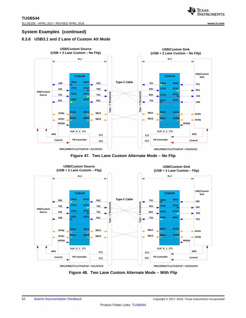
DIR1/DIR0/CTL1/CTL0/FLIP = H/L/H/H/H
USB/Custom Source (USB + 2 Lane Custom ± Flip)
USB/Custom Sink (USB + 2 Lane Custom ± Flip)
DIR1/DIR0/CTL1/CTL0/FLIP = H/H/H/H/H
USB/Custom
Source
TUSB544
SBU1
SBU2
DTX1
DTX2
DRX1
DRX2
PD Controller
CC1
CC2Control
HPDCTLFLIP 0 1
PD Controller
D+/-
HPD
Control
SBU2
SBU1
CTLFLIP 0 1
TX2
TX1
RX2
RX1
D+/-
CC1
CC2
TUSB544
LN0
LN1
UTX1
UTX2
URX1
URX2
DTX1
DTX2
DRX1
DRX2
UTX1
UTX2
URX1
URX2
TX1
TX2
RX1
RX2
LN1
TX2
LN0
RX2
AUXp
AUXn
AUXp
AUXn
SBU1
SBU2
SBU2
SBU1
AUXn
AUXp
Type-C Cable
AUXn
AUXp
TX2
RX2
USB/Custom
Sink
HPDIN HPDIN
Ty
pe
t C
Re
cep
tacl
e
Ty
pe
t C
Re
cep
tacl
e
USB/Custom
Source
TUSB544
SBU1
SBU2
DTX1
DTX2
DRX1
DRX2
PD Controller
CC1
CC2Control
HPDCTLFLIP 0 1
PD Controller
D+/-
HPD
Control
SBU2
SBU1
CTLFLIP 0 1
TX2
TX1
RX2
RX1
D+/-
CC1
CC2
TUSB544
TX1
RX1
UTX1
UTX2
URX1
URX2
DTX1
DTX2
DRX1
DRX2
UTX1
UTX2
URX1
URX2
TX1
TX2
RX1
RX2
DIR1/DIR0/CTL1/CTL0/FLIP = H/L/H/H/L
USB/Custom Source (USB + 2 Lane Custom ± No Flip)
USB/Custom Sink (USB + 2 Lane Custom ± No Flip)
DIR1/DIR0/CTL1/CTL0/FLIP = H/H/H/H/L
TX1
LN1
RX1
LN0
AUXp
AUXn
AUXp
AUXn
SBU1
SBU2 SBU1
SBU2
AUXp
AUXn
Type-C Cable
AUXn
AUXp
LN0
LN1
USB/Custom
Sink
HPDIN HPDIN
Ty
pe
t C
Re
cep
tacl
e
Ty
pe
t C
Re
cep
tacl
e
52
TUSB544SLLSEZ0E –APRIL 2017–REVISED APRIL 2018 www.ti.com
Product Folder Links: TUSB544
Submit Documentation Feedback Copyright © 2017–2018, Texas Instruments Incorporated
System Examples (continued)8.3.6 USB3.1 and 2 Lane of Custom Alt Mode
Figure 47. Two Lane Custom Alternate Mode – No Flip
Figure 48. Two Lane Custom Alternate Mode – With Flip
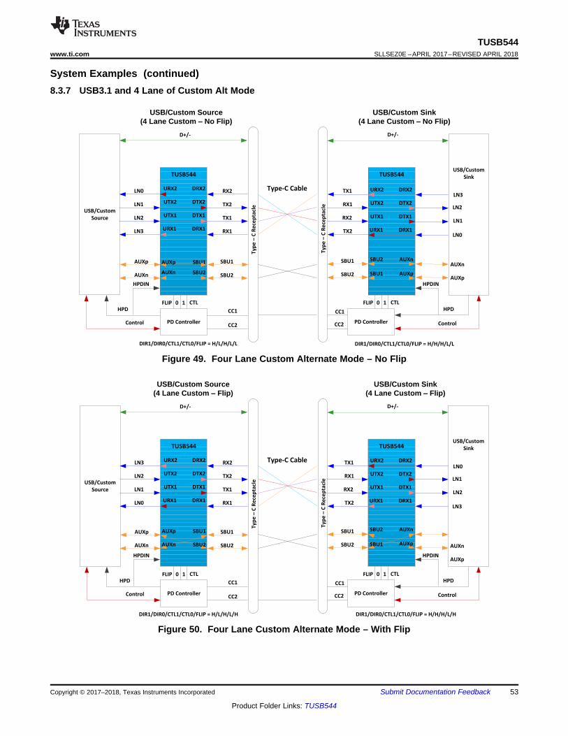
USB/Custom
Source
TUSB544
SBU1
DTX1
DTX2
DRX1
DRX2
SBU2
PD Controller
CC1
CC2Control
HPDCTLFLIP 0 1
PD Controller
D+/-
HPD
Control
SBU2
SBU1
CTLFLIP 0 1
TX2
TX1
RX2
RX1
D+/-
CC1
CC2
TUSB544
UTX1
UTX2
URX1
URX2
DTX1
DTX2
DRX1
DRX2
UTX1
UTX2
URX1
URX2
TX1
TX2
RX1
RX2
DIR1/DIR0/CTL1/CTL0/FLIP = H/L/H/L/H
USB/Custom Source (4 Lane Custom ± Flip)
USB/Custom Sink (4 Lane Custom ± Flip)
DIR1/DIR0/CTL1/CTL0/FLIP = H/H/H/L/H
LN1
LN2
LN0
LN3
AUXp
AUXn
AUXp
AUXn
SBU1
SBU2
Type-C Cable
AUXn
AUXp
LN3
LN0
LN2
LN1
USB/Custom
Sink
HPDIN HPDIN
SBU2
SBU1
AUXn
AUXp
Ty
pe
t C
Re
cep
tacl
e
Ty
pe
t C
Re
cep
tacl
e
USB/Custom
Source
TUSB544
SBU1
SBU2
DTX1
DTX2
DRX1
DRX2
PD Controller
CC1
CC2Control
HPDCTLFLIP 0 1
PD Controller
D+/-
HPD
Control
AUXn
AUXpSBU2
SBU1
CTLFLIP 0 1
TX2
TX1
RX2
RX1
D+/-
CC1
CC2
TUSB544
UTX1
UTX2
URX1
URX2
DTX1
DTX2
DRX1
DRX2
UTX1
UTX2
URX1
URX2
TX1
TX2
RX1
RX2
DIR1/DIR0/CTL1/CTL0/FLIP = H/L/H/L/L
USB/Custom Source (4 Lane Custom ± No Flip)
USB/Custom Sink (4 Lane Custom ± No Flip)
DIR1/DIR0/CTL1/CTL0/FLIP = H/H/H/L/L
LN2
LN1
LN3
LN0
AUXp
AUXn
AUXp
AUXn
SBU1
SBU2
Type-C Cable
LN0
LN3
LN1
LN2
USB/Custom
Sink
HPDIN HPDIN
SBU1
SBU2
AUXp
AUXnT
yp
e t
C R
ece
pta
cle
Ty
pe
t C
Re
cep
tacl
e
53
TUSB544www.ti.com SLLSEZ0E –APRIL 2017–REVISED APRIL 2018
Product Folder Links: TUSB544
Submit Documentation FeedbackCopyright © 2017–2018, Texas Instruments Incorporated
System Examples (continued)8.3.7 USB3.1 and 4 Lane of Custom Alt Mode
Figure 49. Four Lane Custom Alternate Mode – No Flip
Figure 50. Four Lane Custom Alternate Mode – With Flip
54
TUSB544SLLSEZ0E –APRIL 2017–REVISED APRIL 2018 www.ti.com
Product Folder Links: TUSB544
Submit Documentation Feedback Copyright © 2017–2018, Texas Instruments Incorporated
9 Power Supply RecommendationsThe TUSB544 is designed to operate with a 3.3 V power supply. Levels above those listed in the AbsoluteMaximum Ratings table should not be used. If using a higher voltage system power supply, a voltage regulatorcan be used to step down to 3.3 V. Decoupling capacitors should be used to reduce noise and improve powersupply integrity. A 0.1-µF capacitor should be used on each power pin.
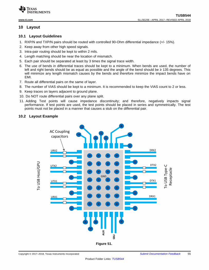
AC Coupling
capacitors
AUX
URX2
DRX1
UTX2
UTX1
URX1
DTX2
DTX1
DRX2
SBU
To
US
B T
yp
e-C
Re
cep
tacl
e
To
US
B H
ost
/GP
U
GND
55
TUSB544www.ti.com SLLSEZ0E –APRIL 2017–REVISED APRIL 2018
Product Folder Links: TUSB544
Submit Documentation FeedbackCopyright © 2017–2018, Texas Instruments Incorporated
10 Layout
10.1 Layout Guidelines1. RXP/N and TXP/N pairs should be routed with controlled 90-Ohm differential impedance (+/- 15%).2. Keep away from other high speed signals.3. Intra-pair routing should be kept to within 2 mils.4. Length matching should be near the location of mismatch.5. Each pair should be separated at least by 3 times the signal trace width.6. The use of bends in differential traces should be kept to a minimum. When bends are used, the number of
left and right bends should be as equal as possible and the angle of the bend should be ≥ 135 degrees. Thiswill minimize any length mismatch causes by the bends and therefore minimize the impact bends have onEMI.
7. Route all differential pairs on the same of layer.8. The number of VIAS should be kept to a minimum. It is recommended to keep the VIAS count to 2 or less.9. Keep traces on layers adjacent to ground plane.10. Do NOT route differential pairs over any plane split.11. Adding Test points will cause impedance discontinuity; and therefore, negatively impacts signal
performance. If test points are used, the test points should be placed in series and symmetrically. The testpoints must not be placed in a manner that causes a stub on the differential pair.
10.2 Layout Example
Figure 51.
56
TUSB544SLLSEZ0E –APRIL 2017–REVISED APRIL 2018 www.ti.com
Product Folder Links: TUSB544
Submit Documentation Feedback Copyright © 2017–2018, Texas Instruments Incorporated
11 Device and Documentation Support
11.1 Documentation Support
11.1.1 Related DocumentationThe documents identified in this section are referenced within this specification. Most references with the text willuse a document tag, identified as [Document Tag], instead of the complete document title to simplify the text.
For related documentation see the following:• [USB31] Universal Serial Bus 3.1 Specification.• [TYPEC] Universal Serial Bus Type C Cable and Connector Specification
11.2 Receiving Notification of Documentation UpdatesTo receive notification of documentation updates, navigate to the device product folder on ti.com. In the upperright corner, click on Alert me to register and receive a weekly digest of any product information that haschanged. For change details, review the revision history included in any revised document.
11.3 Community ResourcesThe following links connect to TI community resources. Linked contents are provided "AS IS" by the respectivecontributors. They do not constitute TI specifications and do not necessarily reflect TI's views; see TI's Terms ofUse.
TI E2E™ Online Community TI's Engineer-to-Engineer (E2E) Community. Created to foster collaborationamong engineers. At e2e.ti.com, you can ask questions, share knowledge, explore ideas and helpsolve problems with fellow engineers.
Design Support TI's Design Support Quickly find helpful E2E forums along with design support tools andcontact information for technical support.
11.4 TrademarksE2E is a trademark of Texas Instruments.All other trademarks are the property of their respective owners.
11.5 Electrostatic Discharge CautionThis integrated circuit can be damaged by ESD. Texas Instruments recommends that all integrated circuits be handled withappropriate precautions. Failure to observe proper handling and installation procedures can cause damage.
ESD damage can range from subtle performance degradation to complete device failure. Precision integrated circuits may be moresusceptible to damage because very small parametric changes could cause the device not to meet its published specifications.
11.6 GlossarySLYZ022 — TI Glossary.
This glossary lists and explains terms, acronyms, and definitions.
12 Mechanical, Packaging, and Orderable InformationThe following pages include mechanical, packaging, and orderable information. This information is the mostcurrent data available for the designated devices. This data is subject to change without notice and revision ofthis document. For browser-based versions of this data sheet, refer to the left-hand navigation.
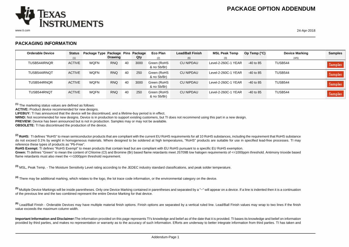
PACKAGE OPTION ADDENDUM
www.ti.com 24-Apr-2018
Addendum-Page 1
PACKAGING INFORMATION
Orderable Device Status(1)
Package Type PackageDrawing
Pins PackageQty
Eco Plan(2)
Lead/Ball Finish(6)
MSL Peak Temp(3)
Op Temp (°C) Device Marking(4/5)
Samples
TUSB544IRNQR ACTIVE WQFN RNQ 40 3000 Green (RoHS& no Sb/Br)
CU NIPDAU Level-2-260C-1 YEAR -40 to 85 TUSB544
TUSB544IRNQT ACTIVE WQFN RNQ 40 250 Green (RoHS& no Sb/Br)
CU NIPDAU Level-2-260C-1 YEAR -40 to 85 TUSB544
TUSB544RNQR ACTIVE WQFN RNQ 40 3000 Green (RoHS& no Sb/Br)
CU NIPDAU Level-2-260C-1 YEAR -40 to 85 TUSB544
TUSB544RNQT ACTIVE WQFN RNQ 40 250 Green (RoHS& no Sb/Br)
CU NIPDAU Level-2-260C-1 YEAR -40 to 85 TUSB544
(1) The marketing status values are defined as follows:ACTIVE: Product device recommended for new designs.LIFEBUY: TI has announced that the device will be discontinued, and a lifetime-buy period is in effect.NRND: Not recommended for new designs. Device is in production to support existing customers, but TI does not recommend using this part in a new design.PREVIEW: Device has been announced but is not in production. Samples may or may not be available.OBSOLETE: TI has discontinued the production of the device.
(2) RoHS: TI defines "RoHS" to mean semiconductor products that are compliant with the current EU RoHS requirements for all 10 RoHS substances, including the requirement that RoHS substancedo not exceed 0.1% by weight in homogeneous materials. Where designed to be soldered at high temperatures, "RoHS" products are suitable for use in specified lead-free processes. TI mayreference these types of products as "Pb-Free".RoHS Exempt: TI defines "RoHS Exempt" to mean products that contain lead but are compliant with EU RoHS pursuant to a specific EU RoHS exemption.Green: TI defines "Green" to mean the content of Chlorine (Cl) and Bromine (Br) based flame retardants meet JS709B low halogen requirements of <=1000ppm threshold. Antimony trioxide basedflame retardants must also meet the <=1000ppm threshold requirement.
(3) MSL, Peak Temp. - The Moisture Sensitivity Level rating according to the JEDEC industry standard classifications, and peak solder temperature.
(4) There may be additional marking, which relates to the logo, the lot trace code information, or the environmental category on the device.
(5) Multiple Device Markings will be inside parentheses. Only one Device Marking contained in parentheses and separated by a "~" will appear on a device. If a line is indented then it is a continuationof the previous line and the two combined represent the entire Device Marking for that device.
(6) Lead/Ball Finish - Orderable Devices may have multiple material finish options. Finish options are separated by a vertical ruled line. Lead/Ball Finish values may wrap to two lines if the finishvalue exceeds the maximum column width.
Important Information and Disclaimer:The information provided on this page represents TI's knowledge and belief as of the date that it is provided. TI bases its knowledge and belief on informationprovided by third parties, and makes no representation or warranty as to the accuracy of such information. Efforts are underway to better integrate information from third parties. TI has taken and
PACKAGE OPTION ADDENDUM
www.ti.com 24-Apr-2018
Addendum-Page 2
continues to take reasonable steps to provide representative and accurate information but may not have conducted destructive testing or chemical analysis on incoming materials and chemicals.TI and TI suppliers consider certain information to be proprietary, and thus CAS numbers and other limited information may not be available for release.
In no event shall TI's liability arising out of such information exceed the total purchase price of the TI part(s) at issue in this document sold by TI to Customer on an annual basis.
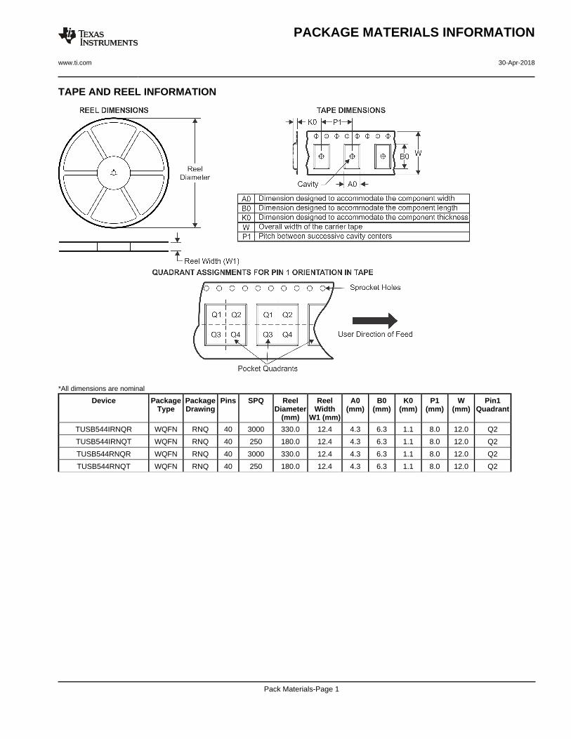
TAPE AND REEL INFORMATION
*All dimensions are nominal
Device PackageType
PackageDrawing
Pins SPQ ReelDiameter
(mm)
ReelWidth
W1 (mm)
A0(mm)
B0(mm)
K0(mm)
P1(mm)
W(mm)
Pin1Quadrant
TUSB544IRNQR WQFN RNQ 40 3000 330.0 12.4 4.3 6.3 1.1 8.0 12.0 Q2
TUSB544IRNQT WQFN RNQ 40 250 180.0 12.4 4.3 6.3 1.1 8.0 12.0 Q2
TUSB544RNQR WQFN RNQ 40 3000 330.0 12.4 4.3 6.3 1.1 8.0 12.0 Q2
TUSB544RNQT WQFN RNQ 40 250 180.0 12.4 4.3 6.3 1.1 8.0 12.0 Q2
PACKAGE MATERIALS INFORMATION
www.ti.com 30-Apr-2018
Pack Materials-Page 1
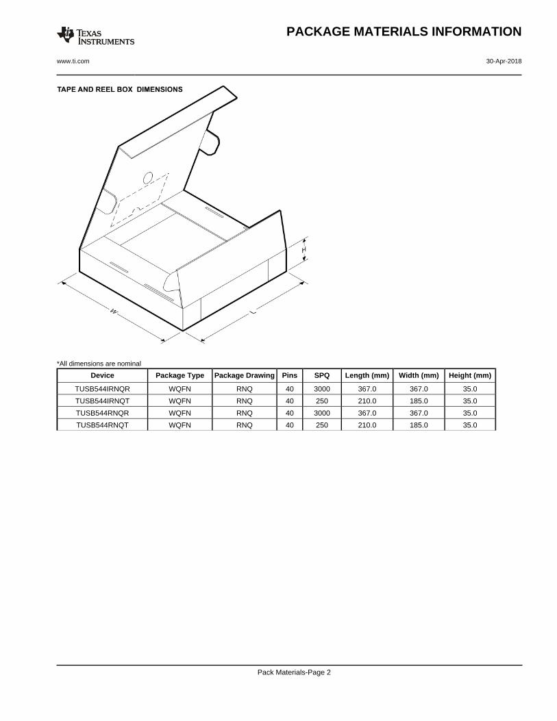
*All dimensions are nominal
Device Package Type Package Drawing Pins SPQ Length (mm) Width (mm) Height (mm)
TUSB544IRNQR WQFN RNQ 40 3000 367.0 367.0 35.0
TUSB544IRNQT WQFN RNQ 40 250 210.0 185.0 35.0
TUSB544RNQR WQFN RNQ 40 3000 367.0 367.0 35.0
TUSB544RNQT WQFN RNQ 40 250 210.0 185.0 35.0
PACKAGE MATERIALS INFORMATION
www.ti.com 30-Apr-2018
Pack Materials-Page 2
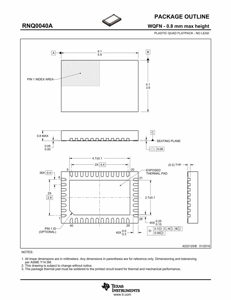
www.ti.com
PACKAGE OUTLINE
C
40X 0.250.15
4.7±0.1
40X 0.50.3
0.8 MAX
(0.2) TYP
0.050.00
36X 0.4
2X2.8
2X 4.4
2.7±0.1
A 6.15.9
B
4.13.9
WQFN - 0.8 mm max heightRNQ0040APLASTIC QUAD FLATPACK - NO LEAD
4222125/B 01/2016
PIN 1 INDEX AREA
0.08
SEATING PLANE
1
8 21
28
9 20
40 29
(OPTIONAL)PIN 1 ID 0.1 C A B
0.05
EXPOSEDTHERMAL PAD
NOTES: 1. All linear dimensions are in millimeters. Any dimensions in parenthesis are for reference only. Dimensioning and tolerancing per ASME Y14.5M. 2. This drawing is subject to change without notice. 3. The package thermal pad must be soldered to the printed circuit board for thermal and mechanical performance.
SCALE 2.500
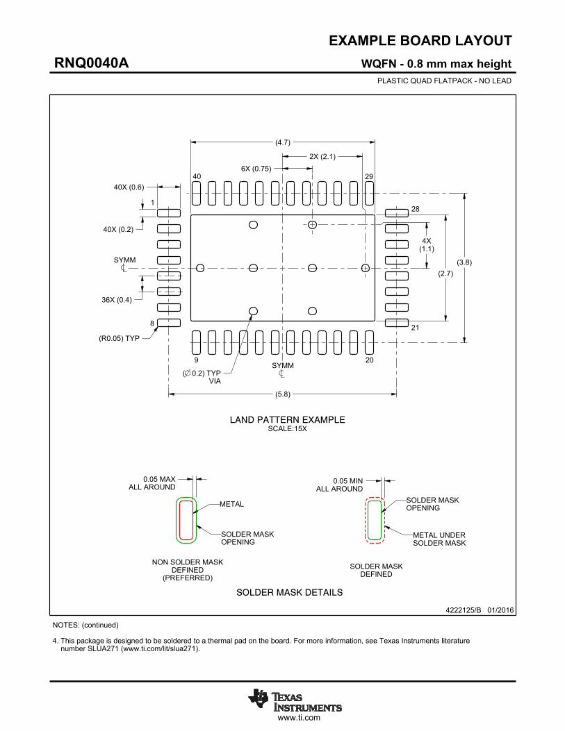
www.ti.com
EXAMPLE BOARD LAYOUT
0.05 MINALL AROUND
0.05 MAXALL AROUND
40X (0.2)
40X (0.6)
( ) TYPVIA
0.2
36X (0.4)
(3.8)
(5.8)
4X(1.1)
(4.7)
(R ) TYP0.05
(2.7)
2X (2.1)6X (0.75)
WQFN - 0.8 mm max heightRNQ0040APLASTIC QUAD FLATPACK - NO LEAD
4222125/B 01/2016
SYMM
1
8
9 20
21
28
2940
SYMM
LAND PATTERN EXAMPLESCALE:15X
NOTES: (continued) 4. This package is designed to be soldered to a thermal pad on the board. For more information, see Texas Instruments literature number SLUA271 (www.ti.com/lit/slua271).
SOLDER MASKOPENING
METAL UNDERSOLDER MASK
SOLDER MASKDEFINED
METAL
SOLDER MASKOPENING
SOLDER MASK DETAILS
NON SOLDER MASKDEFINED
(PREFERRED)
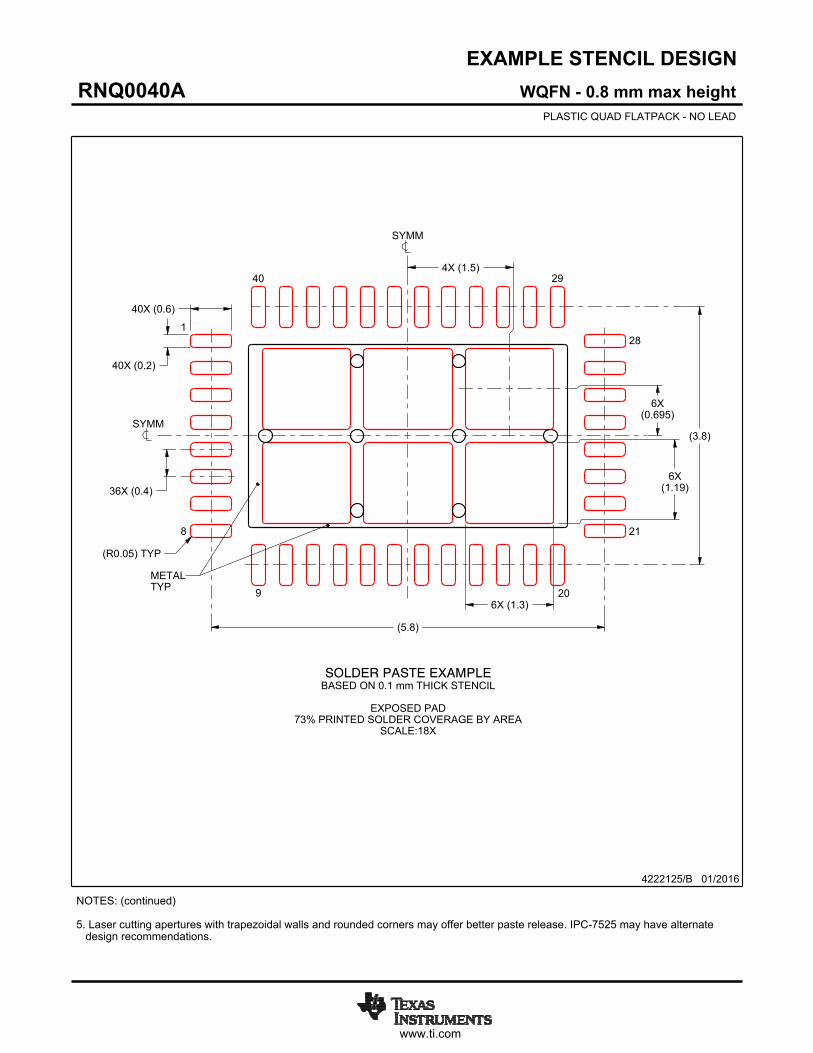
www.ti.com
EXAMPLE STENCIL DESIGN
40X (0.6)
40X (0.2)
36X (0.4)
(5.8)
(3.8)
6X (1.3)
6X(0.695)
4X (1.5)
(R ) TYP0.05
6X(1.19)
WQFN - 0.8 mm max heightRNQ0040APLASTIC QUAD FLATPACK - NO LEAD
4222125/B 01/2016
NOTES: (continued) 5. Laser cutting apertures with trapezoidal walls and rounded corners may offer better paste release. IPC-7525 may have alternate design recommendations.
SYMM
METALTYP
SOLDER PASTE EXAMPLEBASED ON 0.1 mm THICK STENCIL
EXPOSED PAD
73% PRINTED SOLDER COVERAGE BY AREASCALE:18X
SYMM
1
8
9 20
21
28
2940
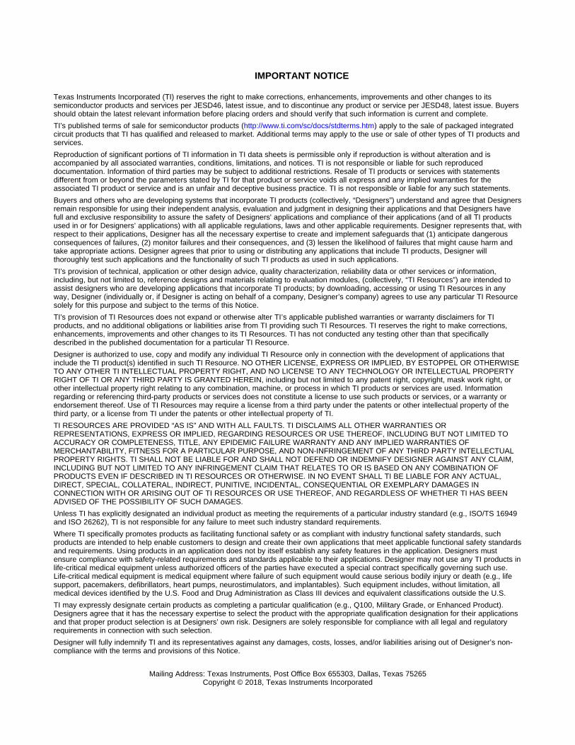
IMPORTANT NOTICE
Texas Instruments Incorporated (TI) reserves the right to make corrections, enhancements, improvements and other changes to itssemiconductor products and services per JESD46, latest issue, and to discontinue any product or service per JESD48, latest issue. Buyersshould obtain the latest relevant information before placing orders and should verify that such information is current and complete.TI’s published terms of sale for semiconductor products (http://www.ti.com/sc/docs/stdterms.htm) apply to the sale of packaged integratedcircuit products that TI has qualified and released to market. Additional terms may apply to the use or sale of other types of TI products andservices.Reproduction of significant portions of TI information in TI data sheets is permissible only if reproduction is without alteration and isaccompanied by all associated warranties, conditions, limitations, and notices. TI is not responsible or liable for such reproduceddocumentation. Information of third parties may be subject to additional restrictions. Resale of TI products or services with statementsdifferent from or beyond the parameters stated by TI for that product or service voids all express and any implied warranties for theassociated TI product or service and is an unfair and deceptive business practice. TI is not responsible or liable for any such statements.Buyers and others who are developing systems that incorporate TI products (collectively, “Designers”) understand and agree that Designersremain responsible for using their independent analysis, evaluation and judgment in designing their applications and that Designers havefull and exclusive responsibility to assure the safety of Designers' applications and compliance of their applications (and of all TI productsused in or for Designers’ applications) with all applicable regulations, laws and other applicable requirements. Designer represents that, withrespect to their applications, Designer has all the necessary expertise to create and implement safeguards that (1) anticipate dangerousconsequences of failures, (2) monitor failures and their consequences, and (3) lessen the likelihood of failures that might cause harm andtake appropriate actions. Designer agrees that prior to using or distributing any applications that include TI products, Designer willthoroughly test such applications and the functionality of such TI products as used in such applications.TI’s provision of technical, application or other design advice, quality characterization, reliability data or other services or information,including, but not limited to, reference designs and materials relating to evaluation modules, (collectively, “TI Resources”) are intended toassist designers who are developing applications that incorporate TI products; by downloading, accessing or using TI Resources in anyway, Designer (individually or, if Designer is acting on behalf of a company, Designer’s company) agrees to use any particular TI Resourcesolely for this purpose and subject to the terms of this Notice.TI’s provision of TI Resources does not expand or otherwise alter TI’s applicable published warranties or warranty disclaimers for TIproducts, and no additional obligations or liabilities arise from TI providing such TI Resources. TI reserves the right to make corrections,enhancements, improvements and other changes to its TI Resources. TI has not conducted any testing other than that specificallydescribed in the published documentation for a particular TI Resource.Designer is authorized to use, copy and modify any individual TI Resource only in connection with the development of applications thatinclude the TI product(s) identified in such TI Resource. NO OTHER LICENSE, EXPRESS OR IMPLIED, BY ESTOPPEL OR OTHERWISETO ANY OTHER TI INTELLECTUAL PROPERTY RIGHT, AND NO LICENSE TO ANY TECHNOLOGY OR INTELLECTUAL PROPERTYRIGHT OF TI OR ANY THIRD PARTY IS GRANTED HEREIN, including but not limited to any patent right, copyright, mask work right, orother intellectual property right relating to any combination, machine, or process in which TI products or services are used. Informationregarding or referencing third-party products or services does not constitute a license to use such products or services, or a warranty orendorsement thereof. Use of TI Resources may require a license from a third party under the patents or other intellectual property of thethird party, or a license from TI under the patents or other intellectual property of TI.TI RESOURCES ARE PROVIDED “AS IS” AND WITH ALL FAULTS. TI DISCLAIMS ALL OTHER WARRANTIES ORREPRESENTATIONS, EXPRESS OR IMPLIED, REGARDING RESOURCES OR USE THEREOF, INCLUDING BUT NOT LIMITED TOACCURACY OR COMPLETENESS, TITLE, ANY EPIDEMIC FAILURE WARRANTY AND ANY IMPLIED WARRANTIES OFMERCHANTABILITY, FITNESS FOR A PARTICULAR PURPOSE, AND NON-INFRINGEMENT OF ANY THIRD PARTY INTELLECTUALPROPERTY RIGHTS. TI SHALL NOT BE LIABLE FOR AND SHALL NOT DEFEND OR INDEMNIFY DESIGNER AGAINST ANY CLAIM,INCLUDING BUT NOT LIMITED TO ANY INFRINGEMENT CLAIM THAT RELATES TO OR IS BASED ON ANY COMBINATION OFPRODUCTS EVEN IF DESCRIBED IN TI RESOURCES OR OTHERWISE. IN NO EVENT SHALL TI BE LIABLE FOR ANY ACTUAL,DIRECT, SPECIAL, COLLATERAL, INDIRECT, PUNITIVE, INCIDENTAL, CONSEQUENTIAL OR EXEMPLARY DAMAGES INCONNECTION WITH OR ARISING OUT OF TI RESOURCES OR USE THEREOF, AND REGARDLESS OF WHETHER TI HAS BEENADVISED OF THE POSSIBILITY OF SUCH DAMAGES.Unless TI has explicitly designated an individual product as meeting the requirements of a particular industry standard (e.g., ISO/TS 16949and ISO 26262), TI is not responsible for any failure to meet such industry standard requirements.Where TI specifically promotes products as facilitating functional safety or as compliant with industry functional safety standards, suchproducts are intended to help enable customers to design and create their own applications that meet applicable functional safety standardsand requirements. Using products in an application does not by itself establish any safety features in the application. Designers mustensure compliance with safety-related requirements and standards applicable to their applications. Designer may not use any TI products inlife-critical medical equipment unless authorized officers of the parties have executed a special contract specifically governing such use.Life-critical medical equipment is medical equipment where failure of such equipment would cause serious bodily injury or death (e.g., lifesupport, pacemakers, defibrillators, heart pumps, neurostimulators, and implantables). Such equipment includes, without limitation, allmedical devices identified by the U.S. Food and Drug Administration as Class III devices and equivalent classifications outside the U.S.TI may expressly designate certain products as completing a particular qualification (e.g., Q100, Military Grade, or Enhanced Product).Designers agree that it has the necessary expertise to select the product with the appropriate qualification designation for their applicationsand that proper product selection is at Designers’ own risk. Designers are solely responsible for compliance with all legal and regulatoryrequirements in connection with such selection.Designer will fully indemnify TI and its representatives against any damages, costs, losses, and/or liabilities arising out of Designer’s non-compliance with the terms and provisions of this Notice.
Mailing Address: Texas Instruments, Post Office Box 655303, Dallas, Texas 75265Copyright © 2018, Texas Instruments Incorporated