Embed Size (px)
Citation preview

1
Santa Clara University School of Engineering
Department of Electrical Engineering Tutorial for Xilinx ISE 7.1i WebPACK and Xilinx Spartan 3 Section I Prepared By: Sally Wood, PhD and Shant Kazanjian (Spring 2006) Section I Outline: I- Project with Xilinx Project Navigator II- Schematic with Xilinx Project Navigator III- Simulation with Xilinx ISE Simulator

I- Project with Xilinx Project Navigator: 1- Open Xilinx ISE 7.1i Project Navigator, you can do that either by double-clicking on the Xilinx ISE 7.1i
desktop icon, or from Start → All Programs → Xilinx ISE 7.1i → Project Navigator
Figure 1. Xilinx Project Navigator initial window
BE CAREFUL: When you open the Xilinx Project Navigator, if you have a previous project already open, then you need to close the old project and proceed with creating a new project.
2- Create a new project, from the menus bar do as follows: File → new project
Project name: tutorial Top-level module type: Schematic Project location: Student’s Z:\ or E:\ drive
2Figure 2. Naming the new project
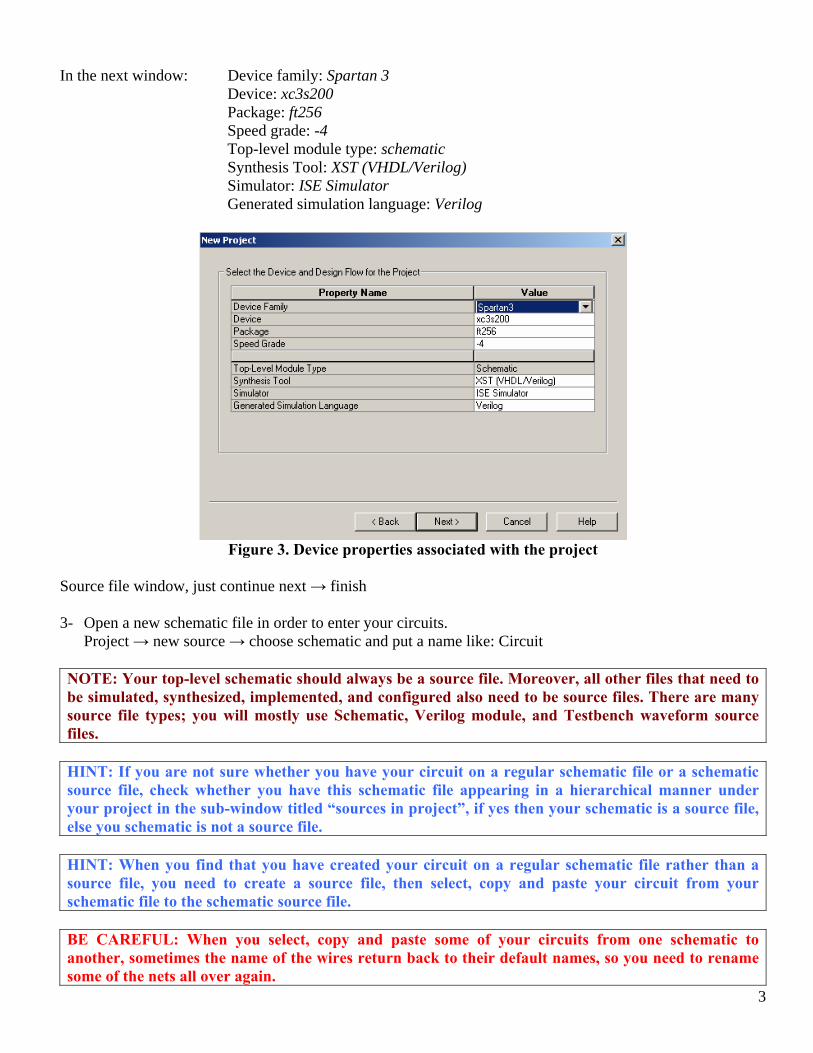
In the next window: Device family: Spartan 3
Device: xc3s200 Package: ft256 Speed grade: -4 Top-level module type: schematic Synthesis Tool: XST (VHDL/Verilog) Simulator: ISE Simulator Generated simulation language: Verilog
Figure 3. Device properties associated with the project
Source file window, just continue next → finish 3- Open a new schematic file in order to enter your circuits. Project → new source → choose schematic and put a name like: Circuit NOTE: Your top-level schematic should always be a source file. Moreover, all other files that need to be simulated, synthesized, implemented, and configured also need to be source files. There are many source file types; you will mostly use Schematic, Verilog module, and Testbench waveform source files.
HINT: If you are not sure whether you have your circuit on a regular schematic file or a schematic source file, check whether you have this schematic file appearing in a hierarchical manner under your project in the sub-window titled “sources in project”, if yes then your schematic is a source file, else you schematic is not a source file.
HINT: When you find that you have created your circuit on a regular schematic file rather than a source file, you need to create a source file, then select, copy and paste your circuit from your schematic file to the schematic source file.
3
BE CAREFUL: When you select, copy and paste some of your circuits from one schematic to another, sometimes the name of the wires return back to their default names, so you need to rename some of the nets all over again.
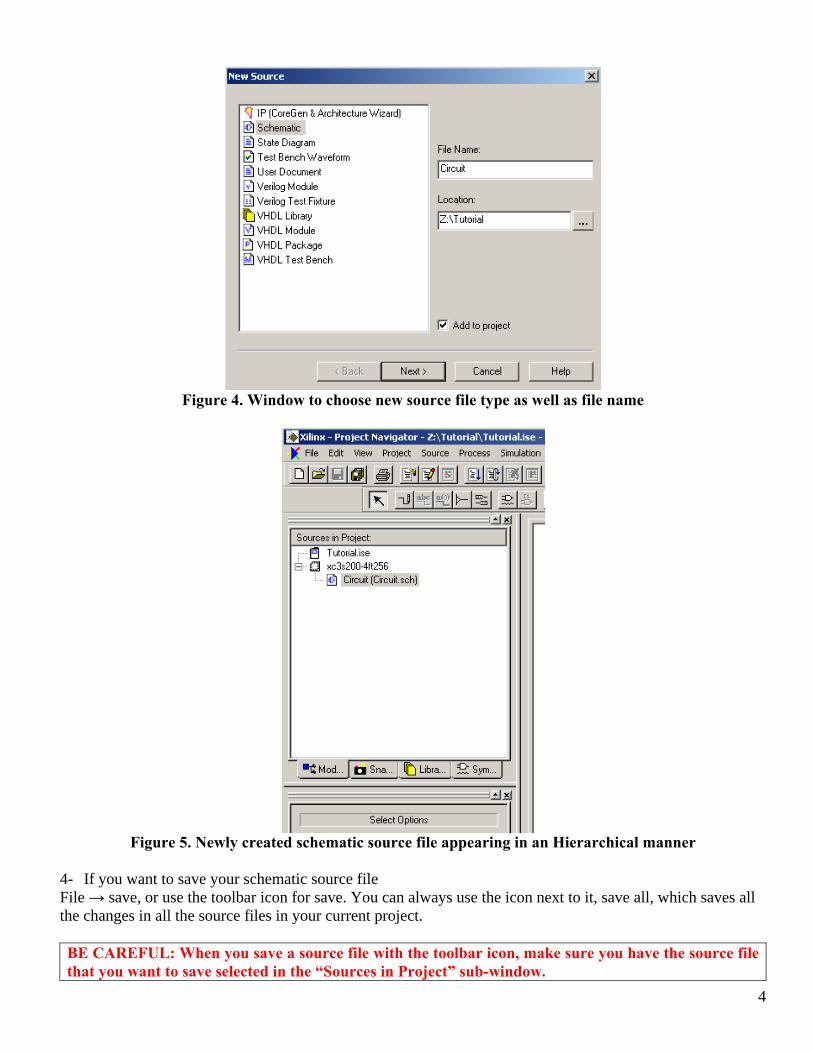
Figure 4. Window to choose new source file type as well as file name
Figure 5. Newly created schematic source file appearing in an Hierarchical manner
4- If you want to save your schematic source file File → save, or use the toolbar icon for save. You can always use the icon next to it, save all, which saves all the changes in all the source files in your current project. BE CAREFUL: When you save a source file with the toolbar icon, make sure you have the source file that you want to save selected in the “Sources in Project” sub-window.
4
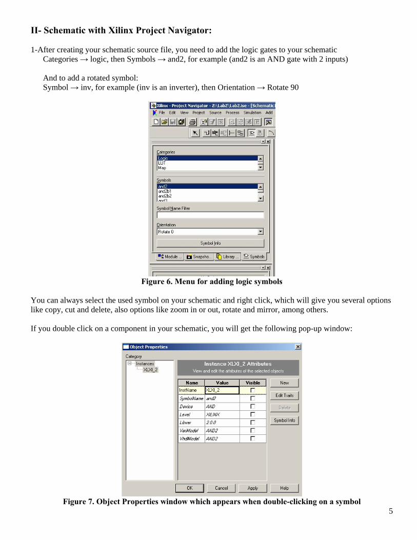
II- Schematic with Xilinx Project Navigator: 1-After creating your schematic source file, you need to add the logic gates to your schematic Categories → logic, then Symbols → and2, for example (and2 is an AND gate with 2 inputs) And to add a rotated symbol: Symbol → inv, for example (inv is an inverter), then Orientation → Rotate 90
Figure 6. Menu for adding logic symbols
You can always select the used symbol on your schematic and right click, which will give you several options like copy, cut and delete, also options like zoom in or out, rotate and mirror, among others. If you double click on a component in your schematic, you will get the following pop-up window:
5Figure 7. Object Properties window which appears when double-clicking on a symbol
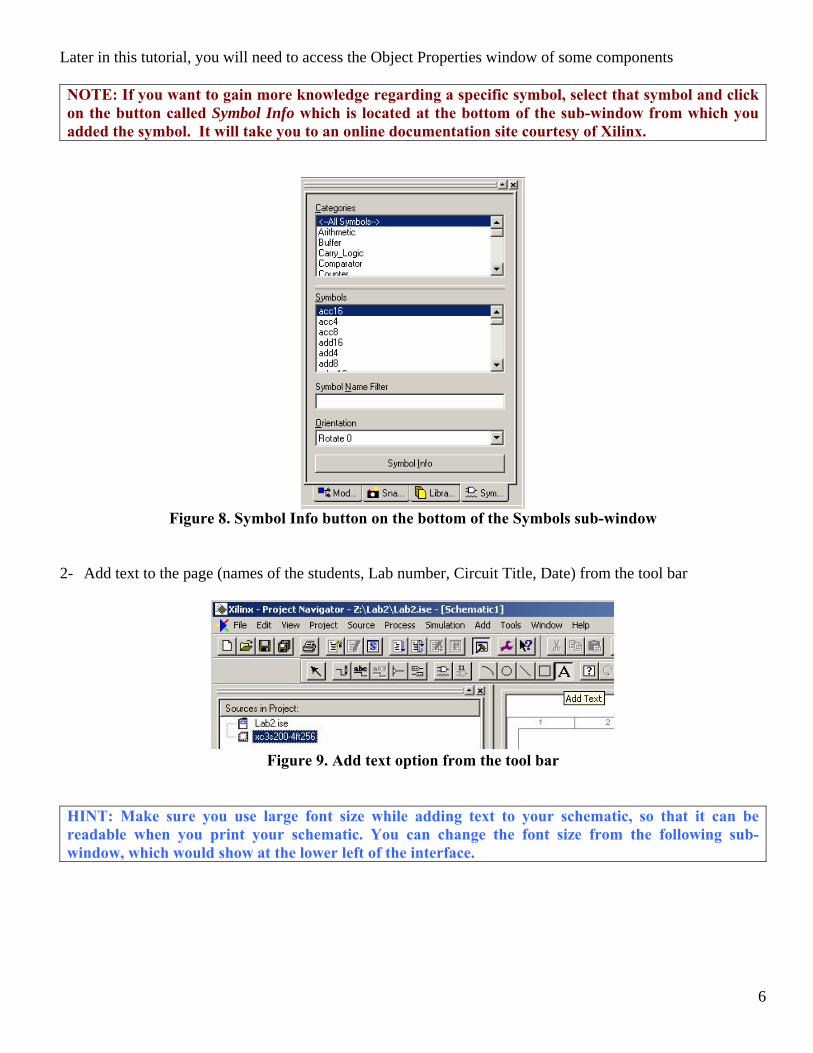
Later in this tutorial, you will need to access the Object Properties window of some components NOTE: If you want to gain more knowledge regarding a specific symbol, select that symbol and click on the button called Symbol Info which is located at the bottom of the sub-window from which you added the symbol. It will take you to an online documentation site courtesy of Xilinx.
Figure 8. Symbol Info button on the bottom of the Symbols sub-window
2- Add text to the page (names of the students, Lab number, Circuit Title, Date) from the tool bar
Figure 9. Add text option from the tool bar
HINT: Make sure you use large font size while adding text to your schematic, so that it can be readable when you print your schematic. You can change the font size from the following sub-window, which would show at the lower left of the interface.
6
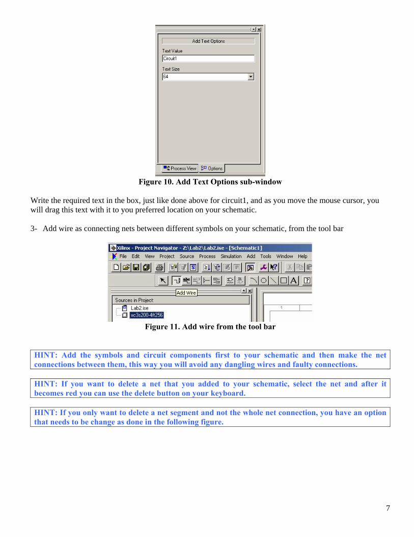
Figure 10. Add Text Options sub-window
Write the required text in the box, just like done above for circuit1, and as you move the mouse cursor, you will drag this text with it to you preferred location on your schematic. 3- Add wire as connecting nets between different symbols on your schematic, from the tool bar
Figure 11. Add wire from the tool bar
HINT: Add the symbols and circuit components first to your schematic and then make the net connections between them, this way you will avoid any dangling wires and faulty connections.
HINT: If you want to delete a net that you added to your schematic, select the net and after it becomes red you can use the delete button on your keyboard.
HINT: If you only want to delete a net segment and not the whole net connection, you have an option that needs to be change as done in the following figure.
7
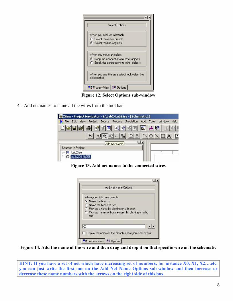
Figure 12. Select Options sub-window
4- Add net names to name all the wires from the tool bar
Figure 13. Add net names to the connected wires
Figure 14. Add the name of the wire and then drag and drop it on that specific wire on the schematic
HINT: If you have a set of net which have increasing set of numbers, for instance X0, X1, X2….etc. you can just write the first one on the Add Net Name Options sub-window and then increase or decrease these name numbers with the arrows on the right side of this box.
8
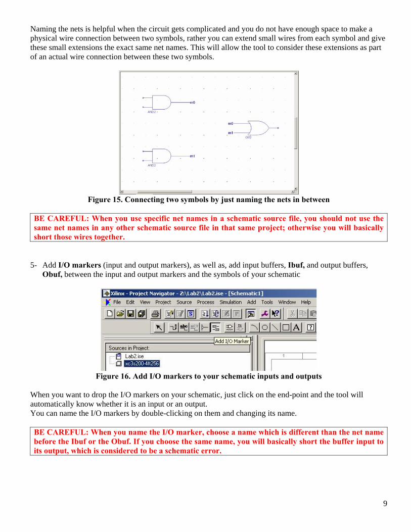
Naming the nets is helpful when the circuit gets complicated and you do not have enough space to make a physical wire connection between two symbols, rather you can extend small wires from each symbol and give these small extensions the exact same net names. This will allow the tool to consider these extensions as part of an actual wire connection between these two symbols.
Figure 15. Connecting two symbols by just naming the nets in between
BE CAREFUL: When you use specific net names in a schematic source file, you should not use the same net names in any other schematic source file in that same project; otherwise you will basically short those wires together.
5- Add I/O markers (input and output markers), as well as, add input buffers, Ibuf, and output buffers,
Obuf, between the input and output markers and the symbols of your schematic
Figure 16. Add I/O markers to your schematic inputs and outputs
When you want to drop the I/O markers on your schematic, just click on the end-point and the tool will automatically know whether it is an input or an output. You can name the I/O markers by double-clicking on them and changing its name. BE CAREFUL: When you name the I/O marker, choose a name which is different than the net name before the Ibuf or the Obuf. If you choose the same name, you will basically short the buffer input to its output, which is considered to be a schematic error.
9
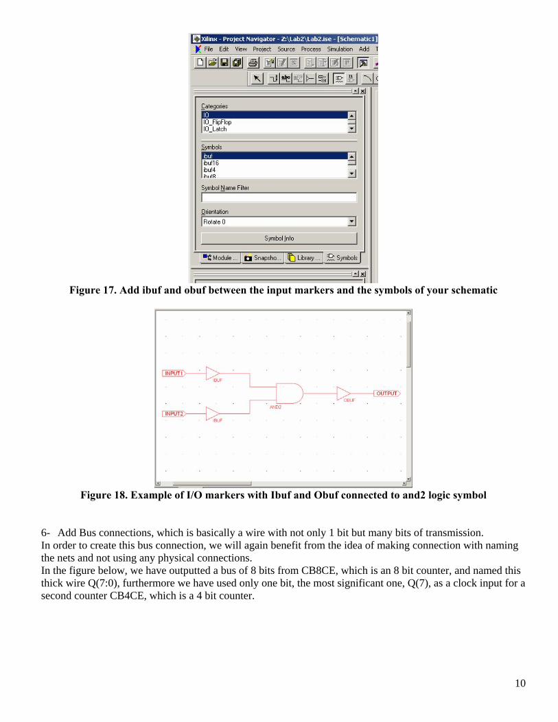
Figure 17. Add ibuf and obuf between the input markers and the symbols of your schematic
Figure 18. Example of I/O markers with Ibuf and Obuf connected to and2 logic symbol
6- Add Bus connections, which is basically a wire with not only 1 bit but many bits of transmission. In order to create this bus connection, we will again benefit from the idea of making connection with naming the nets and not using any physical connections. In the figure below, we have outputted a bus of 8 bits from CB8CE, which is an 8 bit counter, and named this thick wire Q(7:0), furthermore we have used only one bit, the most significant one, Q(7), as a clock input for a second counter CB4CE, which is a 4 bit counter.
10
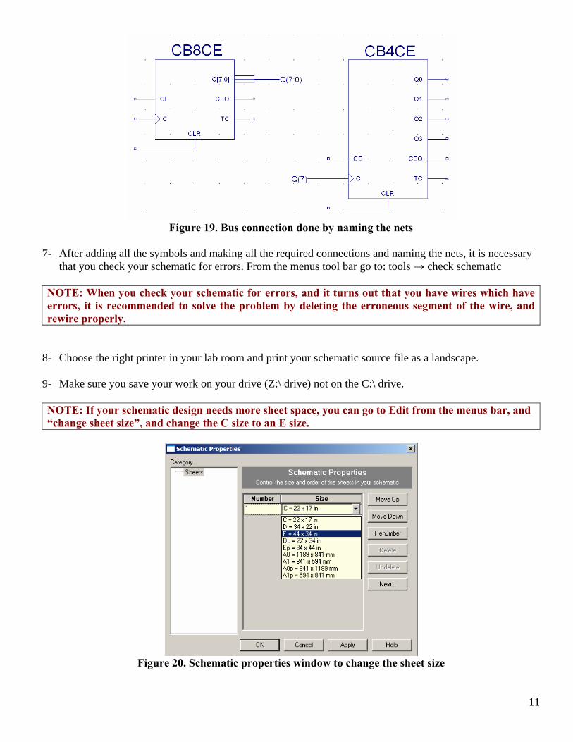
Figure 19. Bus connection done by naming the nets
7- After adding all the symbols and making all the required connections and naming the nets, it is necessary
that you check your schematic for errors. From the menus tool bar go to: tools → check schematic NOTE: When you check your schematic for errors, and it turns out that you have wires which have errors, it is recommended to solve the problem by deleting the erroneous segment of the wire, and rewire properly.
8- Choose the right printer in your lab room and print your schematic source file as a landscape. 9- Make sure you save your work on your drive (Z:\ drive) not on the C:\ drive. NOTE: If your schematic design needs more sheet space, you can go to Edit from the menus bar, and “change sheet size”, and change the C size to an E size.
Figure 20. Schematic properties window to change the sheet size
11
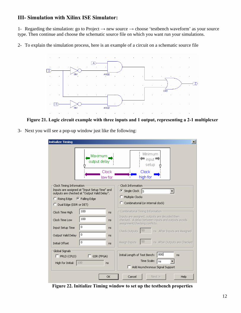
III- Simulation with Xilinx ISE Simulator: 1- Regarding the simulation: go to Project → new source → choose ‘testbench waveform’ as your source type. Then continue and choose the schematic source file on which you want run your simulations. 2- To explain the simulation process, here is an example of a circuit on a schematic source file
Figure 21. Logic circuit example with three inputs and 1 output, representing a 2-1 multiplexer
3- Next you will see a pop-up window just like the following:
Figure 22. Initialize Timing window to set up the testbench properties
12
Make sure you do exactly like done in the previous figure. Change to falling edge, because we want to observe all the possible combination of the three input signals. This example has three inputs, which means there are 23 = 8 distinct input combinations, which explains the reason you should choose ‘Initial Length of Test Bench’ to be 800 nsec, as well as ‘Clock Time High’ and ‘Clock Time Low’ to be 100 nsec. Moreover, in the Clock Information section, select Single Clock, this would be one of the input signals in the circuit.
Figure 23. Initial timing diagram which appears after the Initialize timing window
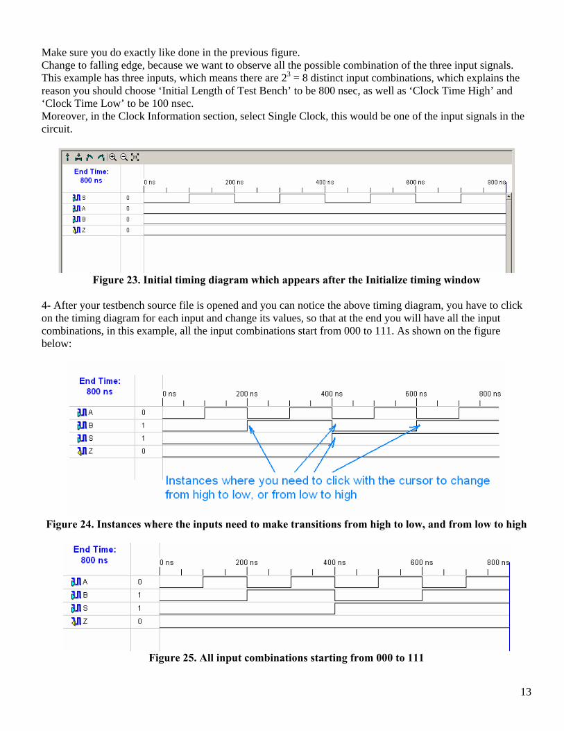
4- After your testbench source file is opened and you can notice the above timing diagram, you have to click on the timing diagram for each input and change its values, so that at the end you will have all the input combinations, in this example, all the input combinations start from 000 to 111. As shown on the figure below:
Figure 24. Instances where the inputs need to make transitions from high to low, and from low to high
Figure 25. All input combinations starting from 000 to 111
13
5- After making sure you have added all the input values, save your testbench source file. NOTE: If your testbench does not appear in the hierarchy of source file in the sub-window ‘Sources in Project’ that means you have not saved you testbench, which you need to do in order to proceed with your simulation.
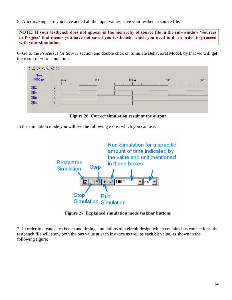
6- Go to the Processes for Source section and double click on Simulate Behavioral Model, by that we will get the result of your simulation.
Figure 26. Correct simulation result at the output
In the simulation mode you will see the following icons, which you can use:
Figure 27. Explained simulation mode taskbar buttons
7- In order to create a testbench and timing simulations of a circuit design which contains bus connections, the testbench file will show both the bus value at each instance as well as each bit value, as shown in the following figure:
14
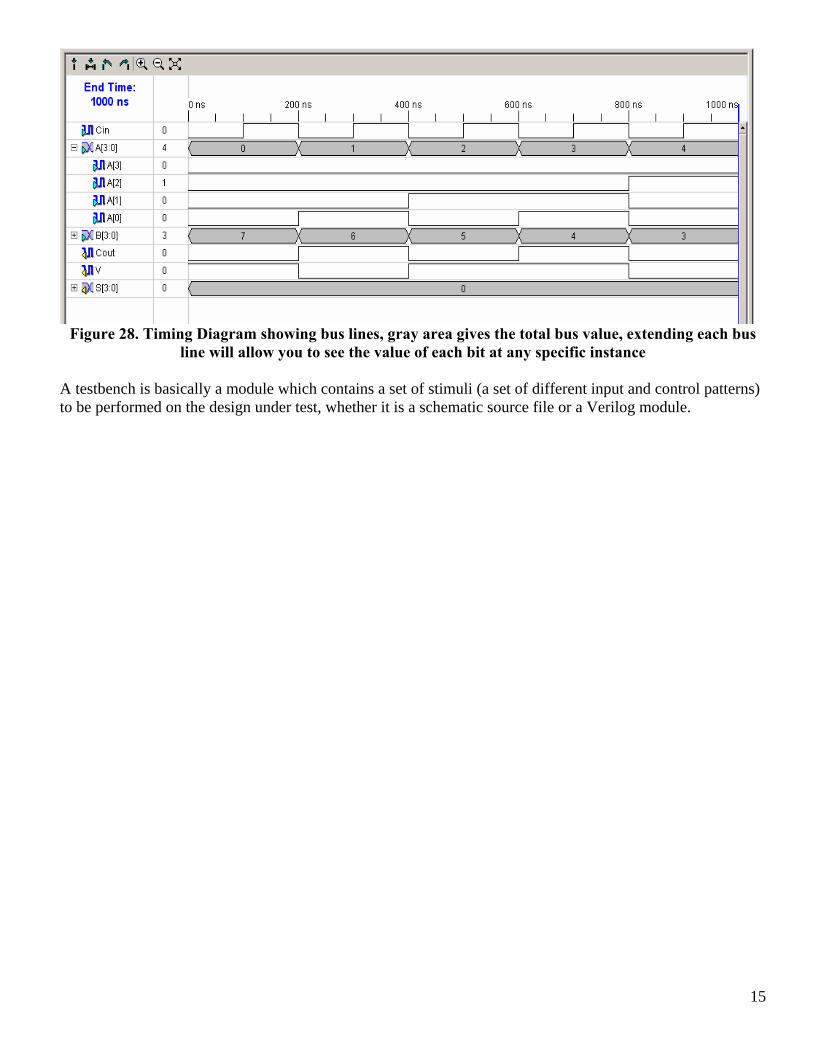
Figure 28. Timing Diagram showing bus lines, gray area gives the total bus value, extending each bus
line will allow you to see the value of each bit at any specific instance A testbench is basically a module which contains a set of stimuli (a set of different input and control patterns) to be performed on the design under test, whether it is a schematic source file or a Verilog module.
15