Embed Size (px)
Citation preview
© Semiconductor Components Industries, LLC, 2013
September, 2013 − Rev. 171 Publication Order Number:
UC3842B/D
UC3842B, UC3843B,UC2842B, UC2843B
High PerformanceCurrent Mode Controllers
The UC3842B, UC3843B series are high performance fixedfrequency current mode controllers. They are specifically designed forOff−Line and DC−DC converter applications offering the designer acost−effective solution with minimal external components. Theseintegrated circuits feature a trimmed oscillator for precise duty cyclecontrol, a temperature compensated reference, high gain erroramplifier, current sensing comparator, and a high current totem poleoutput ideally suited for driving a power MOSFET.
Also included are protective features consisting of input andreference undervoltage lockouts each with hysteresis, cycle−by−cyclecurrent limiting, programmable output deadtime, and a latch for singlepulse metering.
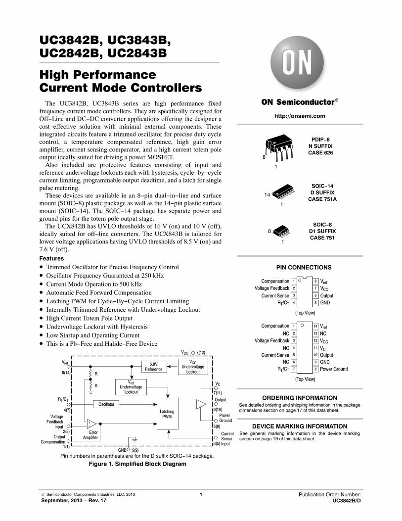
These devices are available in an 8−pin dual−in−line and surfacemount (SOIC−8) plastic package as well as the 14−pin plastic surfacemount (SOIC−14). The SOIC−14 package has separate power andground pins for the totem pole output stage.
The UCX842B has UVLO thresholds of 16 V (on) and 10 V (off),ideally suited for off−line converters. The UCX843B is tailored forlower voltage applications having UVLO thresholds of 8.5 V (on) and7.6 V (off).Features• Trimmed Oscillator for Precise Frequency Control• Oscillator Frequency Guaranteed at 250 kHz• Current Mode Operation to 500 kHz• Automatic Feed Forward Compensation• Latching PWM for Cycle−By−Cycle Current Limiting• Internally Trimmed Reference with Undervoltage Lockout• High Current Totem Pole Output• Undervoltage Lockout with Hysteresis• Low Startup and Operating Current• This is a Pb−Free and Halide−Free Device
Figure 1. Simplified Block Diagram
5.0VReference
LatchingPWM
VCCUndervoltage
Lockout
Oscillator
ErrorAmplifier
7(12)
VC
7(11)
Output
6(10)PowerGround
5(8)
3(5)
CurrentSenseInput
Vref
8(14)
4(7)
2(3)
1(1)GND 5(9)
RT/CT
VoltageFeedback
Input
R
R
+-
VrefUndervoltage
Lockout
OutputCompensation
Pin numbers in parenthesis are for the D suffix SOIC−14 package.
VCC
14
SOIC−14D SUFFIX
CASE 751A1
See detailed ordering and shipping information in the packagedimensions section on page 17 of this data sheet.
ORDERING INFORMATION
See general marking information in the device markingsection on page 19 of this data sheet.
DEVICE MARKING INFORMATION
1
8
PDIP−8N SUFFIXCASE 626
PIN CONNECTIONS
Compensation
NCVoltage Feedback
NCCurrent Sense
NCRT/CT
CompensationVoltage Feedback
Current SenseRT/CT
Vref
Vref
NCVCC
VCOutputGNDPower Ground
VCC
OutputGND
(Top View)
8
7
6
5
1
2
3
4
1
2
3
4
14
13
12
11
5
6
7
10
9
8
(Top View)
SOIC−8D1 SUFFIXCASE 751
1
8
http://onsemi.com
UC3842B, UC3843B, UC2842B, UC2843B
http://onsemi.com2
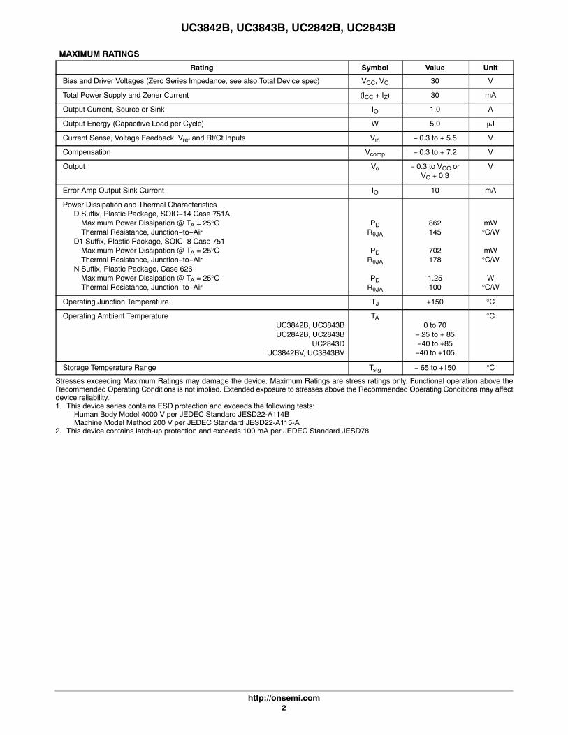
MAXIMUM RATINGS
Rating Symbol Value Unit
Bias and Driver Voltages (Zero Series Impedance, see also Total Device spec) VCC, VC 30 V
Total Power Supply and Zener Current (ICC + IZ) 30 mA
Output Current, Source or Sink IO 1.0 A
Output Energy (Capacitive Load per Cycle) W 5.0 �J
Current Sense, Voltage Feedback, Vref and Rt/Ct Inputs Vin − 0.3 to + 5.5 V
Compensation Vcomp − 0.3 to + 7.2 V
Output Vo − 0.3 to VCC orVC + 0.3
V
Error Amp Output Sink Current IO 10 mA
Power Dissipation and Thermal CharacteristicsD Suffix, Plastic Package, SOIC−14 Case 751A
Maximum Power Dissipation @ TA = 25°CThermal Resistance, Junction−to−Air
D1 Suffix, Plastic Package, SOIC−8 Case 751Maximum Power Dissipation @ TA = 25°CThermal Resistance, Junction−to−Air
N Suffix, Plastic Package, Case 626Maximum Power Dissipation @ TA = 25°CThermal Resistance, Junction−to−Air
PDR�JA
PDR�JA
PDR�JA
862145
702178
1.25100
mW°C/W
mW°C/W
W°C/W
Operating Junction Temperature TJ +150 °C
Operating Ambient TemperatureUC3842B, UC3843BUC2842B, UC2843B
UC2843DUC3842BV, UC3843BV
TA0 to 70
− 25 to + 85−40 to +85−40 to +105
°C
Storage Temperature Range Tstg − 65 to +150 °C
Stresses exceeding Maximum Ratings may damage the device. Maximum Ratings are stress ratings only. Functional operation above theRecommended Operating Conditions is not implied. Extended exposure to stresses above the Recommended Operating Conditions may affectdevice reliability.1. This device series contains ESD protection and exceeds the following tests:
Human Body Model 4000 V per JEDEC Standard JESD22-A114BMachine Model Method 200 V per JEDEC Standard JESD22-A115-A
2. This device contains latch-up protection and exceeds 100 mA per JEDEC Standard JESD78
UC3842B, UC3843B, UC2842B, UC2843B
http://onsemi.com3
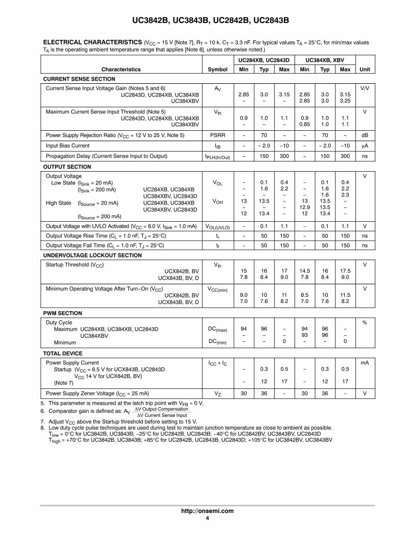
ELECTRICAL CHARACTERISTICS (VCC = 15 V [Note 3], RT = 10 k, CT = 3.3 nF. For typical values TA = 25°C, for min/max valuesTA is the operating ambient temperature range that applies [Note 4], unless otherwise noted.)
UC284XB, UC2843D UC384XB, XBV
Characteristics Symbol Min Typ Max Min Typ Max Unit
REFERENCE SECTION
Reference Output Voltage (IO = 1.0 mA, TJ = 25°C) Vref 4.95 5.0 5.05 4.9 5.0 5.1 V
Line Regulation (VCC = 12 V to 25 V) Regline − 2.0 20 − 2.0 20 mV
Load Regulation (IO = 1.0 mA to 20 mA) Regload − 3.0 25 − 3.0 25 mV
Temperature Stability TS − 0.2 − − 0.2 − mV/°C
Total Output Variation over Line, Load, and TemperatureUC284XBUC2843D
Vref4.94.82
−−
5.15.18
4.82 − 5.18V
Output Noise Voltage (f = 10 Hz to 10 kHz, TJ = 25°C) Vn − 50 − − 50 − �V
Long Term Stability (TA = 125°C for 1000 Hours) S − 5.0 − − 5.0 − mV
Output Short Circuit Current ISC − 30 − 85 −180 − 30 − 85 −180 mA
OSCILLATOR SECTION
FrequencyTJ = 25°CTA = Tlow to ThighTJ = 25°C (RT = 6.2 k, CT = 1.0 nF)
fOSC4948225
52−
250
5556275
4948225
52−
250
5556275
kHz
Frequency Change with Voltage (VCC = 12 V to 25 V) �fOSC/�V − 0.2 1.0 − 0.2 1.0 %
Frequency Change with Temperature, TA = Tlow to Thigh �fOSC/�T − 1.0 − − 0.5 − %
Oscillator Voltage Swing (Peak−to−Peak) VOSC − 1.6 − − 1.6 − V
Discharge Current (VOSC = 2.0 V)TJ = 25°C, TA = Tlow to Thigh
UC284XB, UC384XBUC2843D, UC384XBV
Idischg7.87.5−
8.3−−
8.88.8−
7.87.67.2
8.3−−
8.88.88.8
mA
ERROR AMPLIFIER SECTION
Voltage Feedback Input (VO = 2.5 V) UC284XBUC2843D
VFB 2.452.42
2.52.5
2.552.58
2.42 2.5 2.58 V
Input Bias Current (VFB = 5.0 V) IIB − − 0.1 −1.0 − − 0.1 − 2.0 �A
Open Loop Voltage Gain (VO = 2.0 V to 4.0 V) AVOL 65 90 − 65 90 − dB
Unity Gain Bandwidth (TJ = 25°C) BW 0.7 1.0 − 0.7 1.0 − MHz
Power Supply Rejection Ratio (VCC = 12 V to 25 V) PSRR 60 70 − 60 70 − dB
Output CurrentSink (VO = 1.1 V, VFB = 2.7 V)Source (VO = 5.0 V, VFB = 2.3 V)
ISinkISource
2.0− 0.5
12−1.0
−−
2.0− 0.5
12−1.0
−−
mA
Output Voltage SwingHigh State (RL = 15 k to ground, VFB = 2.3 V)Low State (RL = 15 k to Vref, VFB = 2.7 V)
UC284XB, UC384XBUC2843D, UC384XBV
VOHVOL
5.0
−−
6.2
0.8−
−
1.1−
5.0
−−
6.2
0.80.8
−
1.11.2
V
3. Adjust VCC above the Startup threshold before setting to 15 V.4. Low duty cycle pulse techniques are used during test to maintain junction temperature as close to ambient as possible.
Tlow = 0°C for UC3842B, UC3843B; −25°C for UC2842B, UC2843B; −40°C for UC3842BV, UC3843BV, UC2843DThigh = +70°C for UC3842B, UC3843B; +85°C for UC2842B, UC2843B, UC2843D; +105°C for UC3842BV, UC3843BV
UC3842B, UC3843B, UC2842B, UC2843B
http://onsemi.com4
ELECTRICAL CHARACTERISTICS (VCC = 15 V [Note 7], RT = 10 k, CT = 3.3 nF. For typical values TA = 25°C, for min/max valuesTA is the operating ambient temperature range that applies [Note 8], unless otherwise noted.)
UC284XB, UC2843D UC384XB, XBV
Characteristics Symbol Min Typ Max Min Typ Max Unit
CURRENT SENSE SECTION
Current Sense Input Voltage Gain (Notes 5 and 6)UC2843D, UC284XB, UC384XB
UC384XBV
AV2.85−
3.0−
3.15−
2.852.85
3.03.0
3.153.25
V/V
Maximum Current Sense Input Threshold (Note 5)UC2843D, UC284XB, UC384XB
UC384XBV
Vth0.9−
1.0−
1.1−
0.90.85
1.01.0
1.11.1
V
Power Supply Rejection Ratio (VCC = 12 V to 25 V, Note 5) PSRR − 70 − − 70 − dB
Input Bias Current IIB − − 2.0 −10 − − 2.0 −10 �A
Propagation Delay (Current Sense Input to Output) tPLH(In/Out) − 150 300 − 150 300 ns
OUTPUT SECTION
Output VoltageLow State (ISink = 20 mA)
(ISink = 200 mA) UC284XB, UC384XBUC384XBV, UC2843D
High State (ISource = 20 mA) UC284XB, UC384XBUC384XBV, UC2843D
(ISource = 200 mA)
VOL
VOH
−−−13−12
0.11.6−
13.5−
13.4
0.42.2−−−−
−−−13
12.912
0.11.61.613.513.513.4
0.42.22.3−−−
V
Output Voltage with UVLO Activated (VCC = 6.0 V, ISink = 1.0 mA) VOL(UVLO) − 0.1 1.1 − 0.1 1.1 V
Output Voltage Rise Time (CL = 1.0 nF, TJ = 25°C) tr − 50 150 − 50 150 ns
Output Voltage Fall Time (CL = 1.0 nF, TJ = 25°C) tf − 50 150 − 50 150 ns
UNDERVOLTAGE LOCKOUT SECTION
Startup Threshold (VCC)UCX842B, BV
UCX843B, BV, D
Vth157.8
168.4
179.0
14.57.8
168.4
17.59.0
V
Minimum Operating Voltage After Turn−On (VCC)UCX842B, BV
UCX843B, BV, D
VCC(min)9.07.0
107.6
118.2
8.57.0
107.6
11.58.2
V
PWM SECTION
Duty CycleMaximum UC284XB, UC384XB, UC2843DMaximum UC384XBVMinimum
DC(max)
DC(min)
94−−
96−−
−−0
9493−
9696−
−−0
%
TOTAL DEVICE
Power Supply CurrentStartup (VCC = 6.5 V for UCX843B, UC2843DStartup VCC 14 V for UCX842B, BV)(Note 7)
ICC + IC−
−
0.3
12
0.5
17
−
−
0.3
12
0.5
17
mA
Power Supply Zener Voltage (ICC = 25 mA) VZ 30 36 − 30 36 − V
5. This parameter is measured at the latch trip point with VFB = 0 V.
6. Comparator gain is defined as: AV�V Output Compensation�V Current Sense Input
7. Adjust VCC above the Startup threshold before setting to 15 V.8. Low duty cycle pulse techniques are used during test to maintain junction temperature as close to ambient as possible.
Tlow = 0°C for UC3842B, UC3843B; −25°C for UC2842B, UC2843B; −40°C for UC3842BV, UC3843BV, UC2843DThigh = +70°C for UC3842B, UC3843B; +85°C for UC2842B, UC2843B, UC2843D; +105°C for UC3842BV, UC3843BV
UC3842B, UC3843B, UC2842B, UC2843B
http://onsemi.com5
0.8
2.0
5.0
8.0
20
50
80R
T, T
IMIN
G R
ESIS
TOR
(k)
Ω
1.0 M500 k200 k100 k50 k20 k10 kfOSC, OSCILLATOR FREQUENCY (kHz)
VCC = 15 VTA = 25°C
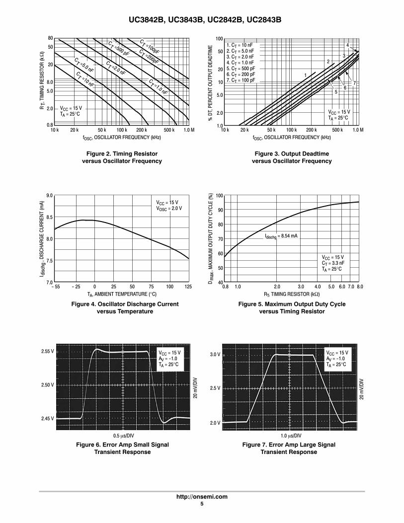
Figure 2. Timing Resistorversus Oscillator Frequency
Figure 3. Output Deadtimeversus Oscillator Frequency
1.0 M500 k200 k100 k50 k20 k10 kfOSC, OSCILLATOR FREQUENCY (kHz)
1.0
2.0
5.0
10
20
50
100
% D
T, P
ERC
ENT
OU
TPU
T D
EAD
TIM
E
1
2
Figure 4. Oscillator Discharge Currentversus Temperature
Figure 5. Maximum Output Duty Cycleversus Timing Resistor
, DIS
CH
ARG
E C
UR
REN
T (m
A)
7.0-�55
TA, AMBIENT TEMPERATURE (°C)-�25 0 25 50 75 100 125
disc
hgI
7.5
8.0
8.5
9.0VCC = 15 VVOSC = 2.0 V
, MAX
IMU
M O
UTP
UT
DU
TY C
YCLE
(%)
max
D 400.8
RT, TIMING RESISTOR (k�)1.0 2.0 3.0 4.0 5.0 6.0 7.0 8.0
50
60
70
80
90
100
VCC = 15 VCT = 3.3 nFTA = 25°C
1. CT = 10 nF2. CT = 5.0 nF3. CT = 2.0 nF4. CT = 1.0 nF5. CT = 500 pF6. CT = 200 pF7. CT = 100 pF
5
Idischg = 8.54 mA
7
3
6
4
VCC = 15 VTA = 25°C
Figure 6. Error Amp Small SignalTransient Response
Figure 7. Error Amp Large SignalTransient Response
1.0 �s/DIV0.5 �s/DIV
20 m
V/D
IV
20 m
V/D
IV
2.55 V
2.50 V
2.45 V
3.0 V
2.5 V
2.0 V
VCC = 15 VAV = -1.0TA = 25°C
VCC = 15 VAV = -1.0TA = 25°C
UC3842B, UC3843B, UC2842B, UC2843B
http://onsemi.com6
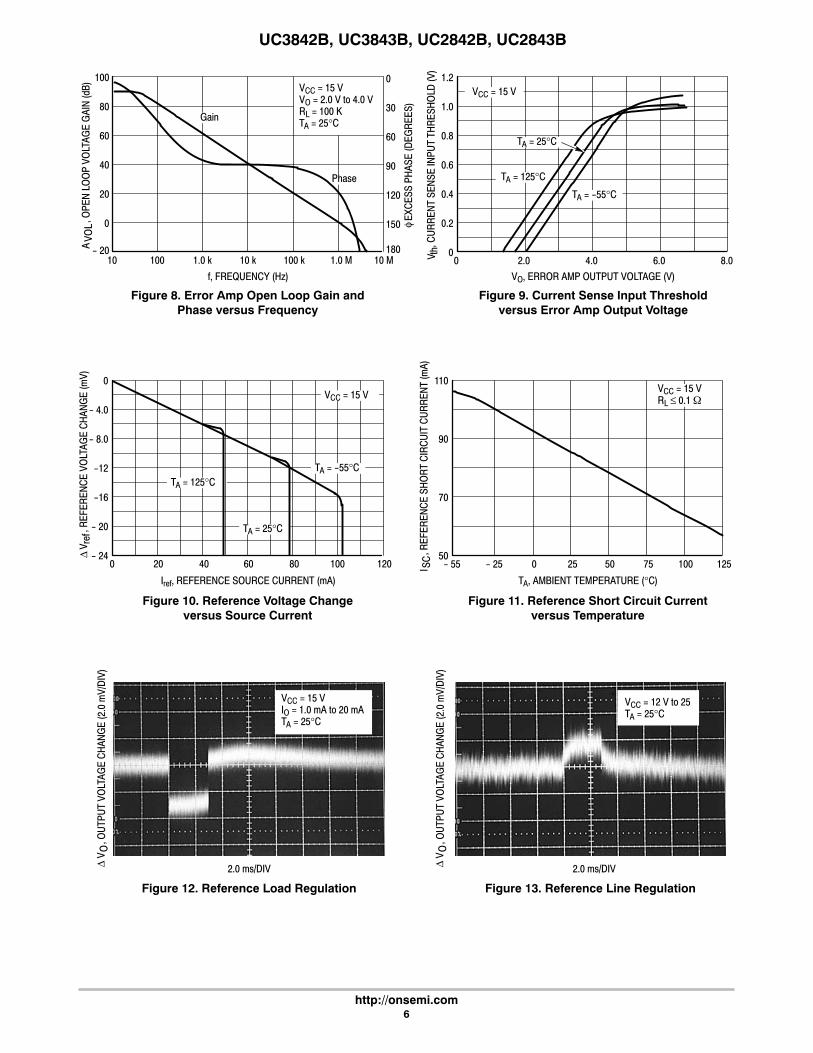
Figure 8. Error Amp Open Loop Gain andPhase versus Frequency
Figure 9. Current Sense Input Thresholdversus Error Amp Output Voltage
Figure 10. Reference Voltage Changeversus Source Current
Figure 11. Reference Short Circuit Currentversus Temperature
-�20AVO
L, O
PEN
LO
OP
VOLT
AGE
GAI
N (d
B)
10 M10
f, FREQUENCY (Hz)
Gain
Phase
VCC = 15 VVO = 2.0 V to 4.0 VRL = 100 KTA = 25°C
0
30
60
90
120
150
180100 1.0 k 10 k 100 k 1.0 M
0
20
40
60
80
100
, EXC
ESS
PHAS
E (D
EGR
EES)
φ
0
VO, ERROR AMP OUTPUT VOLTAGE (V)
0
, CU
RR
ENT
SEN
SE IN
PUT
THR
ESH
OLD
(V)
V th
0.2
0.4
0.6
0.8
1.0
1.2
2.0 4.0 6.0 8.0
VCC = 15 V
TA = 25°C
TA = -55°C
TA = 125°C
ÄÄÄÄVCC = 15 V
ÄÄÄÄÄÄ
TA = -55°C
ÄÄÄÄÄÄÄÄ
TA = 25°C, REF
EREN
CE
VOLT
AGE
CH
ANG
E (m
V)
-16
0
Iref, REFERENCE SOURCE CURRENT (mA)
20 40 60 80 100 120
ref
V
-12
-�8.0
-�4.0
0
Δ
-�20
-�24
ÄÄÄÄTA = 125°C
ÄÄÄÄÄÄVCC = 15 VRL ≤ 0.1 �
, REF
EREN
CE
SHO
RT C
IRC
UIT
CU
RR
ENT
(mA)
SCI
50-�55
TA, AMBIENT TEMPERATURE (°C)
-�25 0 25 50 75 100 125
70
90
110
Figure 12. Reference Load Regulation Figure 13. Reference Line Regulation
2.0 ms/DIV 2.0 ms/DIV
VCC = 15 VIO = 1.0 mA to 20 mATA = 25°C
VCC = 12 V to 25 TA = 25°C
, OU
TPU
T VO
LTAG
E C
HAN
GE
(2.0
mV/
DIV
)V
OΔ
, OU
TPU
T VO
LTAG
E C
HAN
GE
(2.0
mV/
DIV
)V
OΔ
UC3842B, UC3843B, UC2842B, UC2843B
http://onsemi.com7
ÄÄÄÄÄÄÄÄ
Sink Saturation(Load to VCC)
ÄÄÄÄÄÄÄÄ
TA = -�55°C
ÄÄÄVCC
ÄÄÄÄÄÄÄÄÄÄ
Source Saturation(Load to Ground)
0
V sat
, OU
TPU
T SA
TUR
ATIO
N V
OLT
AGE
(V)
8000
IO, OUTPUT LOAD CURRENT (mA)
200 400 600
1.0
2.0
3.0
-�2.0
-1.0
0
ÄÄÄÄÄÄTA = -�55°C
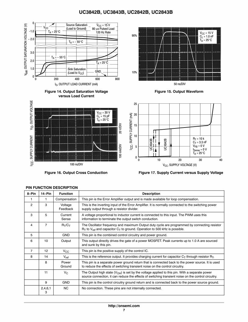
Figure 14. Output Saturation Voltageversus Load Current
Figure 15. Output Waveform
Figure 16. Output Cross Conduction Figure 17. Supply Current versus Supply Voltage
ÄÄÄÄÄÄ
TA = 25°C
ÄÄÄÄÄÄÄÄÄÄÄÄÄÄÄÄ
RT = 10 kCT = 3.3 nFVFB = 0 VISense = 0 VTA = 25°C
, SU
PPLY
CU
RR
ENT
(mA)
CC
I
00
VCC, SUPPLY VOLTAGE (V)
10 20 30 40
5
10
15
20
25
UC
X843
B
UC
X842
B
ÄÄÄÄÄÄÄÄ
TA = 25°C
ÄÄGND
ÄÄÄÄÄÄÄÄÄÄÄÄÄÄÄ
VCC = 15 V80 �s Pulsed Load
120 Hz Rate
VCC = 30 VCL = 15 pFTA = 25°C
VCC = 15 VCL = 1.0 nFTA = 25°C
50 ns/DIV
100 ns/DIV
100
mA/
DIV
20 V
/DIV
90%
10%
, OU
TPU
T VO
LTAG
EO
V, S
UPP
LY C
UR
REN
TC
CI
PIN FUNCTION DESCRIPTION
8−Pin 14−Pin Function Description
1 1 Compensation This pin is the Error Amplifier output and is made available for loop compensation.
2 3 VoltageFeedback
This is the inverting input of the Error Amplifier. It is normally connected to the switching powersupply output through a resistor divider.
3 5 CurrentSense
A voltage proportional to inductor current is connected to this input. The PWM uses thisinformation to terminate the output switch conduction.
4 7 RT/CT The Oscillator frequency and maximum Output duty cycle are programmed by connecting resistorRT to Vref and capacitor CT to ground. Operation to 500 kHz is possible.
5 GND This pin is the combined control circuitry and power ground.
6 10 Output This output directly drives the gate of a power MOSFET. Peak currents up to 1.0 A are sourcedand sunk by this pin.
7 12 VCC This pin is the positive supply of the control IC.
8 14 Vref This is the reference output. It provides charging current for capacitor CT through resistor RT.
8 PowerGround
This pin is a separate power ground return that is connected back to the power source. It is usedto reduce the effects of switching transient noise on the control circuitry.
11 VC The Output high state (VOH) is set by the voltage applied to this pin. With a separate powersource connection, it can reduce the effects of switching transient noise on the control circuitry.
9 GND This pin is the control circuitry ground return and is connected back to the power source ground.
2,4,6,13
NC No connection. These pins are not internally connected.
UC3842B, UC3843B, UC2842B, UC2843B
http://onsemi.com8
OPERATING DESCRIPTION
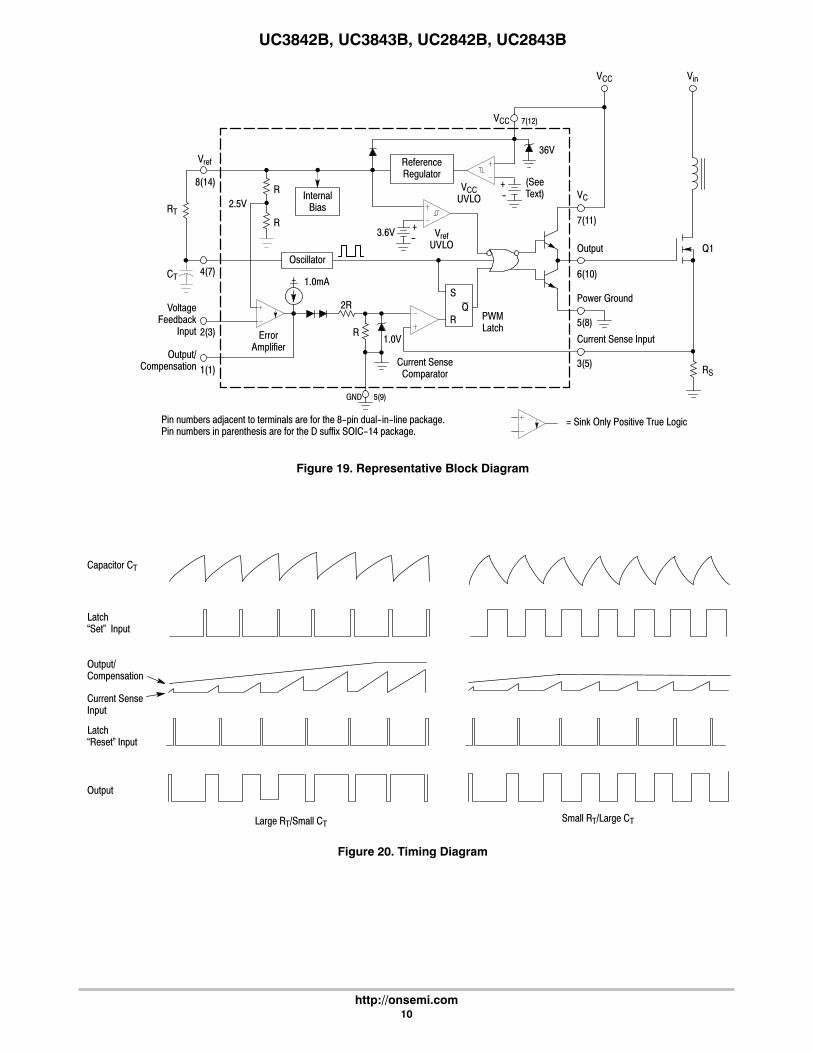
The UC3842B, UC3843B series are high performance,fixed frequency, current mode controllers. They arespecifically designed for Off−Line and DC−to−DCconverter applications offering the designer a cost−effectivesolution with minimal external components. Arepresentative block diagram is shown in Figure 19.
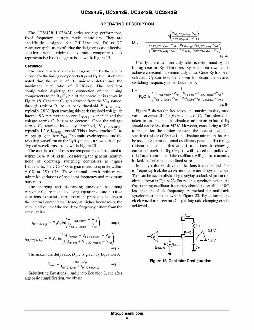
OscillatorThe oscillator frequency is programmed by the values
chosen for the timing components RT and CT. It must also benoted that the value of RT uniquely determines themaximum duty ratio of UC384xx. The oscillatorconfiguration depicting the connection of the timingcomponents to the RT/CT pin of the controller is shown inFigure 18. Capacitor CT gets charged from the Vref source,through resistor RT to its peak threshold VRT/CT(peak),typically 2.8 V. Upon reaching this peak threshold volage, aninternal 8.3 mA current source, Idischg, is enabled and thevoltage across CT begins to decrease. Once the voltageacross CT reaches its valley threshold, VRT/CT(valley),typically 1.2 V, Idischg turns off. This allows capacitor CT tocharge up again from Vref. This entire cycle repeats, and theresulting waveform on the RT/CT pin has a sawtooth shape.Typical waveforms are shown in Figure 20.
The oscillator thresholds are temperature compensated towithin ±6% at 50 kHz. Considering the general industrytrend of operating switching controllers at higherfrequencies, the UC384xx is guaranteed to operate within±10% at 250 kHz. These internal circuit refinementsminimize variations of oscillator frequency and maximumduty ratio.
The charging and discharging times of the timingcapacitor CT are calculated using Equations 1 and 2. Theseequations do not take into account the propagation delays ofthe internal comparator. Hence, at higher frequencies, thecalculated value of the oscillator frequency differs from theactual value.
tRT�CT(chg) � RTCT ln�VRT�CT(valley) � Vref
VRT�CT(peak) � Vref� (eq. 1)
tRT�CT(dischg) � RTCT ln�RTIdischg � VRT�CT(peak) � Vref
RTIdischg � VRT�CT(valley) � Vref�(eq. 2)
The maximum duty ratio, Dmax is given by Equation 3.
Dmax �tRT�CT(chg)
tRT�CT(chg) � tRT�CT(dischg)(eq. 3)
Substituting Equations 1 and 2 into Equation 3, and afteralgebraic simplification, we obtain
Dmax �
ln�VRT�CT(valley)�Vref
VRT�CT(peak)�Vref�
ln�VRT�CT(valley)�Vref
VRT�CT(peak)�Vref�
RTIdischg�VRT�CT(peak)�Vref
RTIdischg�VRT�CT(valley)�Vref�(eq. 4)
Clearly, the maximum duty ratio is determined by thetiming resistor RT. Therefore, RT is chosen such as toachieve a desired maximum duty ratio. Once RT has beenselected, CT can now be chosen to obtain the desiredswitching frequency as per Equation 5.
f � 1
RTCT ln�VRT�CT(valley)�Vref
VRT�CT(peak)�Vref�
RTIdischg�VRT�CT(peak)�Vref
RTIdischg�VRT�CT(valley)�Vref�
(eq. 5)
Figure 2 shows the frequency and maximum duty ratiovariation versus RT for given values of CT. Care should betaken to ensure that the absolute minimum value of RTshould not be less than 542 �. However, considering a 10%tolerance for the timing resistor, the nearest availablestandard resistor of 680 � is the absolute minimum that canbe used to guarantee normal oscillator operation. If a timingresistor smaller than this value is used, then the chargingcurrent through the RT, CT path will exceed the pulldown(discharge) current and the oscillator will get permanentlylocked/latched to an undefined state.
In many noise-sensitive applications it may be desirableto frequency-lock the converter to an external system clock.This can be accomplished by applying a clock signal to the
circuit shown in Figure 22. For reliable synchronization, thefree-running oscillator frequency should be set about 10%less than the clock frequency. A method for multi-unitsynchronization is shown in Figure 23. By tailoring theclock waveform, accurate Output duty ratio clamping can beachieved.
EnableIdischg
Vref
RT/CT
RT
CT
2.8 V
1.2 V
Figure 18. Oscillator Configuration
UC3842B, UC3843B, UC2842B, UC2843B
http://onsemi.com9
Error AmplifierA fully compensated Error Amplifier with access to the
inverting input and output is provided. It features a typicalDC voltage gain of 90 dB, and a unity gain bandwidth of1.0 MHz with 57 degrees of phase margin (Figure 8). Thenon−inverting input is internally biased at 2.5 V and is notpinned out. The converter output voltage is typically divideddown and monitored by the inverting input. The maximuminput bias current is −2.0 �A which can cause an outputvoltage error that is equal to the product of the input biascurrent and the equivalent input divider source resistance.
The Error Amp Output (Pin 1) is provided for externalloop compensation (Figure 33). The output voltage is offsetby two diode drops (≈1.4 V) and divided by three before itconnects to the non−inverting input of the Current SenseComparator. This guarantees that no drive pulses appear atthe Output (Pin 6) when pin 1 is at its lowest state (VOL).This occurs when the power supply is operating and the loadis removed, or at the beginning of a soft−start interval(Figures 25, 26). The Error Amp minimum feedbackresistance is limited by the amplifier’s source current(0.5 mA) and the required output voltage (VOH) to reach thecomparator’s 1.0 V clamp level:
Rf(min) ≈3.0 (1.0 V) + 1.4 V
0.5 mA = 8800 �
Current Sense Comparator and PWM LatchThe UC3842B, UC3843B operate as a current mode
controller, whereby output switch conduction is initiated bythe oscillator and terminated when the peak inductor currentreaches the threshold level established by the ErrorAmplifier Output/Compensation (Pin 1). Thus the errorsignal controls the peak inductor current on acycle−by−cycle basis. The Current Sense Comparator PWMLatch configuration used ensures that only a single pulse
appears at the Output during any given oscillator cycle. Theinductor current is converted to a voltage by inserting theground−referenced sense resistor RS in series with thesource of output switch Q1. This voltage is monitored by theCurrent Sense Input (Pin 3) and compared to a level derivedfrom the Error Amp Output. The peak inductor current undernormal operating conditions is controlled by the voltage atpin 1 where:
Ipk =V(Pin 1) − 1.4 V
3 RS
Abnormal operating conditions occur when the powersupply output is overloaded or if output voltage sensing islost. Under these conditions, the Current Sense Comparatorthreshold will be internally clamped to 1.0 V. Therefore themaximum peak switch current is:
Ipk(max) =1.0 VRS
When designing a high power switching regulator itbecomes desirable to reduce the internal clamp voltage inorder to keep the power dissipation of RS to a reasonablelevel. A simple method to adjust this voltage is shown inFigure 24. The two external diodes are used to compensatethe internal diodes, yielding a constant clamp voltage overtemperature. Erratic operation due to noise pickup can resultif there is an excessive reduction of the Ipk(max) clampvoltage.
A narrow spike on the leading edge of the currentwaveform can usually be observed and may cause the powersupply to exhibit an instability when the output is lightlyloaded. This spike is due to the power transformerinterwinding capacitance and output rectifier recovery time.The addition of an RC filter on the Current Sense Input witha time constant that approximates the spike duration willusually eliminate the instability (refer to Figure 28).
UC3842B, UC3843B, UC2842B, UC2843B
http://onsemi.com10
+-
ReferenceRegulator
VCCUVLO
+- Vref
UVLO3.6V
36V
S
RQ
InternalBias
+ 1.0mA
Oscillator
2.5VR
R
R
2R
ErrorAmplifier
VoltageFeedback
Input
Output/Compensation Current Sense
Comparator
1.0V
VCC 7(12)
GND 5(9)
VC
7(11)
Output
6(10)
Power Ground
5(8)
Current Sense Input
3(5)RS
Q1
VCC Vin
1(1)
2(3)
4(7)
8(14)
RT
CT
Vref
= Sink Only Positive True LogicPin numbers adjacent to terminals are for the 8-pin dual-in-line package.Pin numbers in parenthesis are for the D suffix SOIC-14 package.
Figure 19. Representative Block Diagram
Figure 20. Timing Diagram
Large RT/Small CTSmall RT/Large CT
PWMLatch
(SeeText)
Capacitor CT
Latch“Set" Input
Output/Compensation
Current SenseInput
Latch“Reset" Input
Output
UC3842B, UC3843B, UC2842B, UC2843B
http://onsemi.com11
Undervoltage LockoutTwo undervoltage lockout comparators have been
incorporated to guarantee that the IC is fully functionalbefore the output stage is enabled. The positive powersupply terminal (VCC) and the reference output (Vref) areeach monitored by separate comparators. Each has built−inhysteresis to prevent erratic output behavior as theirrespective thresholds are crossed. The VCC comparatorupper and lower thresholds are 16 V/10 V for the UCX842B,and 8.4 V/7.6 V for the UCX843B. The Vref comparatorupper and lower thresholds are 3.6 V/3.4 V. The largehysteresis and low startup current of the UCX842B makesit ideally suited in off−line converter applications whereefficient bootstrap startup techniques are required(Figure 35). The UCX843B is intended for lower voltageDC−to−DC converter applications. A 36 V Zener isconnected as a shunt regulator from VCC to ground. Itspurpose is to protect the IC from excessive voltage that canoccur during system startup. The minimum operatingvoltage (VCC) for the UCX842B is 11 V and 8.2 V for theUCX843B.
These devices contain a single totem pole output stage thatwas specifically designed for direct drive of powerMOSFETs. It is capable of up to ±1.0 A peak drive currentand has a typical rise and fall time of 50 ns with a 1.0 nF load.Additional internal circuitry has been added to keep theOutput in a sinking mode whenever an undervoltage lockoutis active. This characteristic eliminates the need for anexternal pull−down resistor.
The SOIC−14 surface mount package provides separatepins for VC (output supply) and Power Ground. Properimplementation will significantly reduce the level ofswitching transient noise imposed on the control circuitry.This becomes particularly useful when reducing the Ipk(max)clamp level. The separate VC supply input allows thedesigner added flexibility in tailoring the drive voltageindependent of VCC. A Zener clamp is typically connectedto this input when driving power MOSFETs in systemswhere VCC is greater than 20 V. Figure 27 shows properpower and control ground connections in a current−sensingpower MOSFET application.
ReferenceThe 5.0 V bandgap reference is trimmed to ±1.0%
tolerance at TJ = 25°C on the UC284XB, and ±2.0% on theUC384XB. Its primary purpose is to supply charging currentto the oscillator timing capacitor. The reference has short−circuit protection and is capable of providing in excess of20 mA for powering additional control system circuitry.
Design ConsiderationsDo not attempt to construct the converter on
wire−wrap or plug−in prototype boards. High frequencycircuit layout techniques are imperative to preventpulse−width jitter. This is usually caused by excessive noisepick−up imposed on the Current Sense or Voltage Feedbackinputs. Noise immunity can be improved by lowering circuitimpedances at these points. The printed circuit layout shouldcontain a ground plane with low−current signal andhigh−current switch and output grounds returning onseparate paths back to the input filter capacitor. Ceramicbypass capacitors (0.1 �F) connected directly to VCC, VC,and Vref may be required depending upon circuit layout.This provides a low impedance path for filtering the highfrequency noise. All high current loops should be kept asshort as possible using heavy copper runs to minimizeradiated EMI. The Error Amp compensation circuitry andthe converter output voltage divider should be located closeto the IC and as far as possible from the power switch andother noise−generating components.
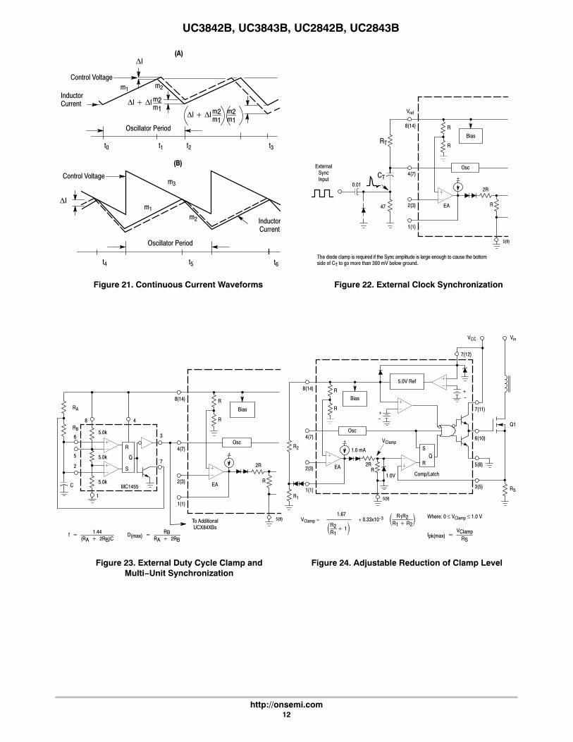
Current mode converters can exhibit subharmonicoscillations when operating at a duty cycle greater than 50%with continuous inductor current. This instability isindependent of the regulator’s closed loop characteristicsand is caused by the simultaneous operating conditions offixed frequency and peak current detecting. Figure 21Ashows the phenomenon graphically. At t0, switchconduction begins, causing the inductor current to rise at aslope of m1. This slope is a function of the input voltagedivided by the inductance. At t1, the Current Sense Inputreaches the threshold established by the control voltage.This causes the switch to turn off and the current to decay ata slope of m2, until the next oscillator cycle. The unstablecondition can be shown if a perturbation is added to thecontrol voltage, resulting in a small �I (dashed line). Witha fixed oscillator period, the current decay time is reduced,and the minimum current at switch turn−on (t2) is increasedby �I + �I m2/m1. The minimum current at the next cycle(t3) decreases to (�I + �I m2/m1) (m2/m1). This perturbationis multiplied by m2/m1 on each succeeding cycle, alternatelyincreasing and decreasing the inductor current at switchturn−on. Several oscillator cycles may be required beforethe inductor current reaches zero causing the process tocommence again. If m2/m1 is greater than 1, the converterwill be unstable. Figure 21B shows that by adding anartificial ramp that is synchronized with the PWM clock tothe control voltage, the �I perturbation will decrease to zeroon succeeding cycles. This compensating ramp (m3) musthave a slope equal to or slightly greater than m2/2 forstability. With m2/2 slope compensation, the averageinductor current follows the control voltage, yielding truecurrent mode operation. The compensating ramp can bederived from the oscillator and added to either the VoltageFeedback or Current Sense inputs (Figure 34).
UC3842B, UC3843B, UC2842B, UC2843B
http://onsemi.com12
Figure 21. Continuous Current Waveforms
2(3) EA
Bias
+
Osc
R
R
R
2R
5(9)
1(1)
4(7)
8(14)
RT
CT
Vref
0.01
The diode clamp is required if the Sync amplitude is large enough to cause the bottomside of CT to go more than 300 mV below ground.
ExternalSyncInput
47
+
R
R
R
2R
Bias
Osc
EA
5(9)
1(1)
2(3)
4(7)
8(14)
To AdditionalUCX84XBs
R
S
Q
8 4
6
5
2
1
C
3
7
RA
RB5.0k
5.0k
5.0kMC1455
f� �� 1.44(RA� �� 2RB)C
D(max) ��� RBRA ��� 2RB
+-
5.0V Ref
+-
S
RQ
Bias
+
Osc
R
R
R2REA
1.0V
5(9)
7(11)
6(10)
5(8)
3(5) RS
Q1
VCC Vin
1(1)
2(3)
4(7)
8(14)
R1
VClampR2
7(12)
Comp/Latch
1.0 mA
Ipk(max)� �VClamp
RS
Where: 0 ≤ VClamp ≤ 1.0 VVClamp ≈1.67
�R2R1
� 1�+ 0.33x10⁻³ � R1R2
R1 � R2�
Control Voltage
InductorCurrent
Oscillator Period
Control Voltage
InductorCurrent
Oscillator Period
(A)
(B)
m1 m2
t0 t1 t2 t3
m3
m2
t4 t5 t6
�I
m1�I
�l � �l m2m1
�l � �l m2m1
��� m2m1
Figure 22. External Clock Synchronization
Figure 23. External Duty Cycle Clamp andMulti−Unit Synchronization
Figure 24. Adjustable Reduction of Clamp Level
UC3842B, UC3843B, UC2842B, UC2843B
http://onsemi.com13
+-
+-
S
R
+
R
R
R2R
VClamp �� 1.67
�R2R1
� 1�
Ipk(max)� �VClamp
RS
5.0V Ref
Q
Bias
Osc
EA
1.0V
5(9)
7(11)
6(10)
5(8)
3(5)RS
Q1
VCC Vin
1(1)
2(3)
4(7)
8(14)
R1
VClamp
R2
Where: 0 ≤ VClamp ≤ 1.0 V
C MPSA63
tSoftStart � � In1 �� VC3�VClamp
��CR1�R2
R1 ��� R2
7(12)
1.0 mA
Comp/Latch
5.0V Ref
+-
S
RQ
Bias
+
1.0mA
Osc
R
R
R2R
EA 1.0V
5(9)
1(1)
2(3)
4(7)
8(14)
C
1.0M
tSoft-Start ≈ 3600C in �F
Figure 25. Soft−Start Circuit Figure 26. Adjustable Buffered Reduction ofClamp Level with Soft−Start
+-
5.0V Ref
+-
S
RQ
(11)
(10)
(8)
Comp/Latch
(5) RS1/4 W
VCC Vin
K
M
D SENSEFET
GS
Power Ground:To Input Source
Return
Control Circuitry Ground:To Pin (9)
Virtually lossless current sensing can be achieved with the implementation of aSENSEFET power switch. For proper operation during over-current conditions, areduction of the Ipk(max) clamp level must be implemented. Refer to Figures 24 and 26.
VPin 5 RS Ipk rDS(on)rDM(on) � RS
If: SENSEFET = MTP10N10MRS = 200
Then :� VPin�5� � 0.075�Ipk
(12)
Figure 27. Current Sensing Power MOSFET
+-
5.0V Ref
+-
S
RQ
7(11)
6(10)
5(8)
3(5)
RS
Q1
VCC Vin
C
R
The addition of the RC filter will eliminate instability caused by the leadingedge spike on the current waveform.
7(12)
Comp/Latch
Figure 28. Current Waveform Spike Suppression
UC3842B, UC3843B, UC2842B, UC2843B
http://onsemi.com14
Figure 29. MOSFET Parasitic Oscillations
6(10)
5(8)
3(5) RS
Q1
Vin
C1
Base ChargeRemoval
The totem pole output can furnish negative base current for enhancedtransistor turn-off, with the addition of capacitor C1.
S
R
5.0V Ref
Q
7(11)
6(10)
5(8)
3(5)
RS
Q1
VCC
IB
+
-
0
Vin
IsolationBoundary
VGS Waveforms
+
-0
+
-
0
50% DC 25% DC
Ipk �V(Pin1) � 1.4
3�RS��NS
Np�
Comp/Latch
7(12)
R
C NS NP
+-
+-
Bias
+
Osc
R
R
R
2R
EA
5(9)
1(1)
2(3)
4(7)
8(14)
The MCR101 SCR must be selected for a holding of < 0.5 mA @ TA(min). The simple twotransistor circuit can be used in place of the SCR as shown. All resistors are 10 k.
MCR101
2N3905
2N3903
1.0 mA
S
R
5.0V Ref
Q
7(11)
6(10)
5(8)
3(5) RS
Q1
VCC Vin
Series gate resistor Rg will damp any high frequency parasitic oscillationscaused by the MOSFET input capacitance and any series wiring inductance inthe gate-source circuit.
7(12)
Rg
Comp/Latch
+-
+-
Figure 30. Bipolar Transistor Drive
Figure 31. Isolated MOSFET Drive Figure 32. Latched Shutdown
UC3842B, UC3843B, UC2842B, UC2843B
http://onsemi.com15
+-
+-
5.0V Ref
36V
S
RQ
Bias
+1.0mA
Osc
R
R
R
2R
EA 1.0V
7(12)
7(11)
6(10)
5(8)
3(5) RS
VCC Vin
1(1)
2(3)
4(7)
8(14)RT
CT
The buffered oscillator ramp can be resistively summed with either the voltagefeedback or current sense inputs to provide slope compensation.
m- 3.0m
-m
RfCf
Ri
Rd
From VORSlope
MPS3904
5(9)
Comp/Latch
Figure 33. Error Amplifier Compensation
+
R
2R1.0mA
EA
2(3)
5(9)
2.5V
1(1)
RfCfRd
Ri
From VO
Error Amp compensation circuit for stabilizing any current mode topology except for boost and flybackconverters operating with continuous inductor current.
Rf ≥ 8.8 k
+
R
2R1.0mA
EA
2(3)
5(9)
2.5V
1(1)
RfCfRd
Rp
From VO
Error Amp compensation circuit for stabilizing current mode boost and flybacktopologies operating with continuous inductor current.
Cp
Ri
Figure 34. Slope Compensation
UC3842B, UC3843B, UC2842B, UC2843B
http://onsemi.com16
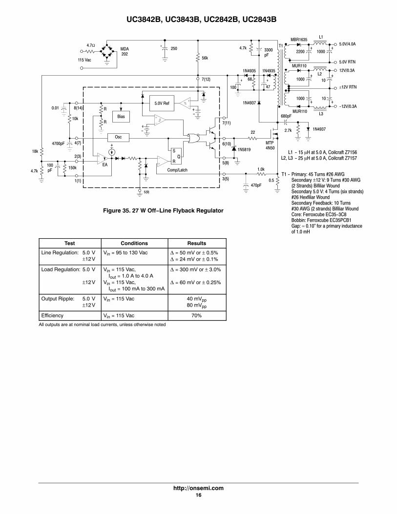
Figure 35. 27 W Off−Line Flyback Regulator
MUR110+-
+-
S
R
+
R
R
5.0V Ref
Q
Bias
EA
5(9)
7(11)
6(10)
5(8)
3(5) 0.5
MTP4N50
1(1)
2(3)
4(7)
8(14)
10k
4700pF
470pF
150k100pF
18k
4.7k
0.01
100
+
1.0k
115 Vac
4.7�MDA202
250
56k
4.7k 3300pF
1N4935 1N4935
+ +68
47
1N4937
1N4937
680pF
2.7k
L3
L2
L1
+ +
+ +
+ +
1000
1000
2200
10
10
1000
5.0V/4.0A
5.0V RTN
12V/0.3A
±12V RTN
-12V/0.3A
Primary: 45 Turns #26 AWGSecondary ±12 V: 9 Turns #30 AWG(2 Strands) Bifiliar WoundSecondary 5.0 V: 4 Turns (six strands)#26 Hexfiliar WoundSecondary Feedback: 10 Turns#30 AWG (2 strands) Bifiliar WoundCore: Ferroxcube EC35-3C8Bobbin: Ferroxcube EC35PCB1Gap: ≈ 0.10" for a primary inductanceof 1.0 mH
MUR110
MBR1635T1
22Osc
T1 -
7(12)
Comp/Latch
L1L2, L3
- 15 �H at 5.0 A, Coilcraft Z7156- 25 �H at 5.0 A, Coilcraft Z7157
1N5819
Test Conditions Results
Line Regulation: 5.0 V±12V
Vin = 95 to 130 Vac � = 50 mV or ± 0.5%� = 24 mV or ± 0.1%
Load Regulation: 5.0 V
±12V
Vin = 115 Vac, Iout = 1.0 A to 4.0 A
Vin = 115 Vac, Iout = 100 mA to 300 mA
� = 300 mV or ± 3.0%
� = 60 mV or ± 0.25%
Output Ripple: 5.0 V±12V
Vin = 115 Vac 40 mVpp80 mVpp
Efficiency Vin = 115 Vac 70%
All outputs are at nominal load currents, unless otherwise noted
UC3842B, UC3843B, UC2842B, UC2843B
http://onsemi.com17
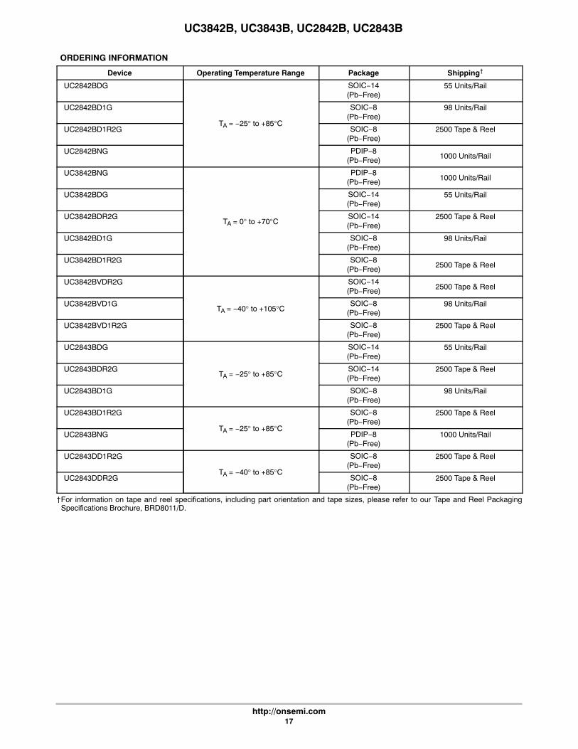
ORDERING INFORMATION
Device Operating Temperature Range Package Shipping†
UC2842BDG
TA = −25° to +85°C
SOIC−14(Pb−Free)
55 Units/Rail
UC2842BD1G SOIC−8(Pb−Free)
98 Units/Rail
UC2842BD1R2G SOIC−8(Pb−Free)
2500 Tape & Reel
UC2842BNG PDIP−8(Pb−Free) 1000 Units/Rail
UC3842BNG
TA = 0° to +70°C
PDIP−8(Pb−Free) 1000 Units/Rail
UC3842BDG SOIC−14(Pb−Free)
55 Units/Rail
UC3842BDR2G SOIC−14(Pb−Free)
2500 Tape & Reel
UC3842BD1G SOIC−8(Pb−Free)
98 Units/Rail
UC3842BD1R2G SOIC−8(Pb−Free) 2500 Tape & Reel
UC3842BVDR2G
TA = −40° to +105°C
SOIC−14(Pb−Free) 2500 Tape & Reel
UC3842BVD1G SOIC−8(Pb−Free)
98 Units/Rail
UC3842BVD1R2G SOIC−8(Pb−Free)
2500 Tape & Reel
UC2843BDG
TA = −25° to +85°C
SOIC−14(Pb−Free)
55 Units/Rail
UC2843BDR2G SOIC−14(Pb−Free)
2500 Tape & Reel
UC2843BD1G SOIC−8(Pb−Free)
98 Units/Rail
UC2843BD1R2G
TA = −25° to +85°C
SOIC−8(Pb−Free)
2500 Tape & Reel
UC2843BNG PDIP−8(Pb−Free)
1000 Units/Rail
UC2843DD1R2G
TA = −40° to +85°C
SOIC−8(Pb−Free)
2500 Tape & Reel
UC2843DDR2G SOIC−8(Pb−Free)
2500 Tape & Reel
†For information on tape and reel specifications, including part orientation and tape sizes, please refer to our Tape and Reel PackagingSpecifications Brochure, BRD8011/D.
UC3842B, UC3843B, UC2842B, UC2843B
http://onsemi.com18
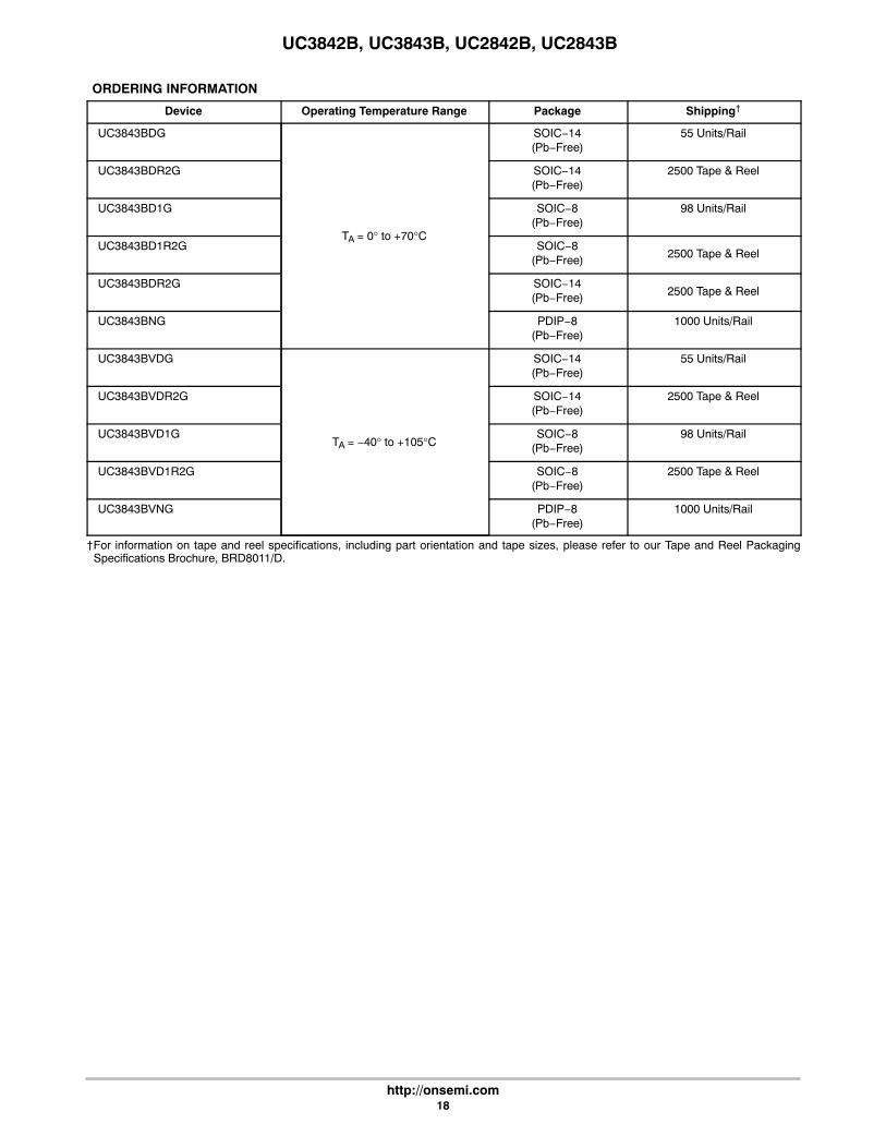
ORDERING INFORMATION
Device Operating Temperature Range Package Shipping†
UC3843BDG
TA = 0° to +70°C
SOIC−14(Pb−Free)
55 Units/Rail
UC3843BDR2G SOIC−14(Pb−Free)
2500 Tape & Reel
UC3843BD1G SOIC−8(Pb−Free)
98 Units/Rail
UC3843BD1R2G SOIC−8(Pb−Free) 2500 Tape & Reel
UC3843BDR2G SOIC−14(Pb−Free) 2500 Tape & Reel
UC3843BNG PDIP−8(Pb−Free)
1000 Units/Rail
UC3843BVDG
TA = −40° to +105°C
SOIC−14(Pb−Free)
55 Units/Rail
UC3843BVDR2G SOIC−14(Pb−Free)
2500 Tape & Reel
UC3843BVD1G SOIC−8(Pb−Free)
98 Units/Rail
UC3843BVD1R2G SOIC−8(Pb−Free)
2500 Tape & Reel
UC3843BVNG PDIP−8(Pb−Free)
1000 Units/Rail
†For information on tape and reel specifications, including part orientation and tape sizes, please refer to our Tape and Reel PackagingSpecifications Brochure, BRD8011/D.
UC3842B, UC3843B, UC2842B, UC2843B
http://onsemi.com19
SOIC−14D SUFFIX
CASE 751A
SOIC−8D1 SUFFIXCASE 751
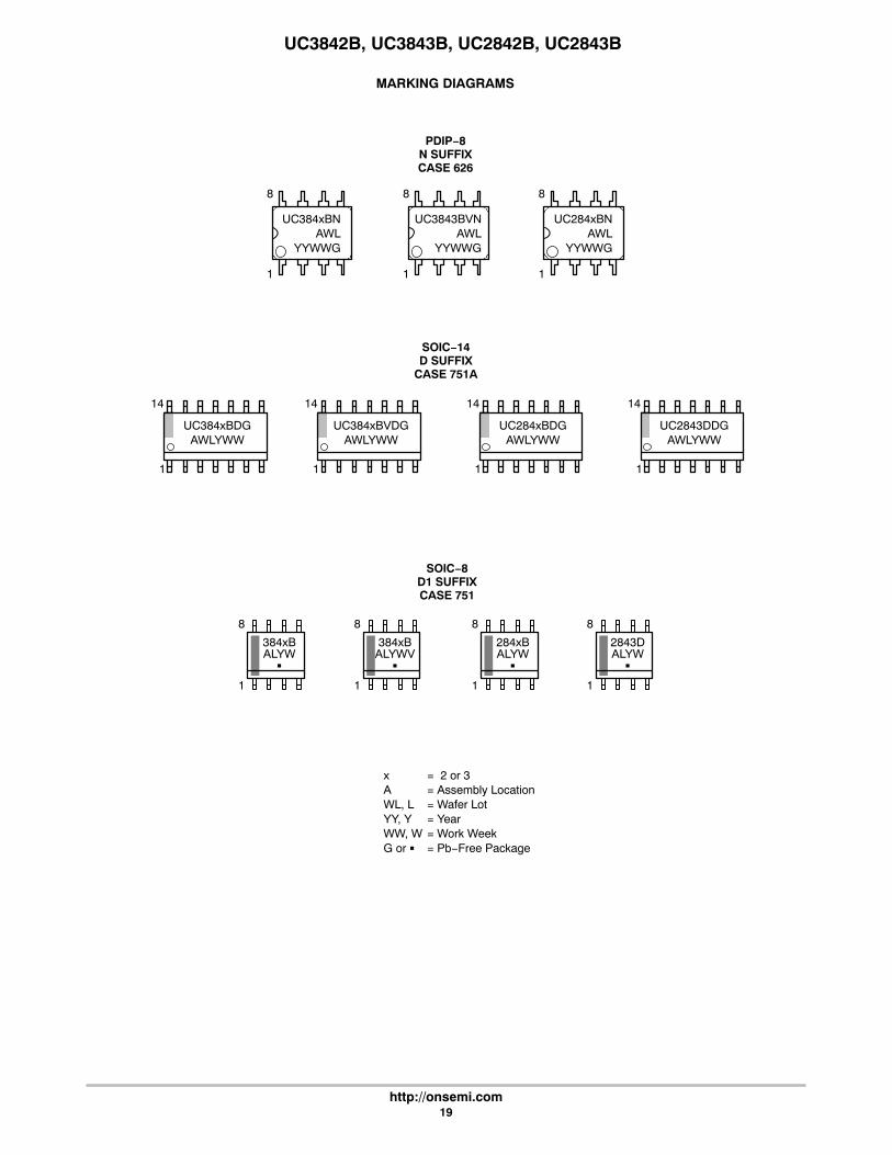
MARKING DIAGRAMS
PDIP−8N SUFFIXCASE 626
x = 2 or 3A = Assembly LocationWL, L = Wafer LotYY, Y = YearWW, W = Work WeekG or � = Pb−Free Package
UC3843BVNAWL
YYWWG
1
8
UC384xBVDGAWLYWW
1
14
384xBALYWV
�
1
8
UC384xBNAWL
YYWWG
1
8
UC284xBNAWL
YYWWG
1
8
UC384xBDGAWLYWW
1
14
UC284xBDGAWLYWW
1
14
384xBALYW
�
1
8
284xBALYW
�
1
8
UC2843DDGAWLYWW
1
14
2843DALYW
�
1
8
UC3842B, UC3843B, UC2842B, UC2843B
http://onsemi.com20
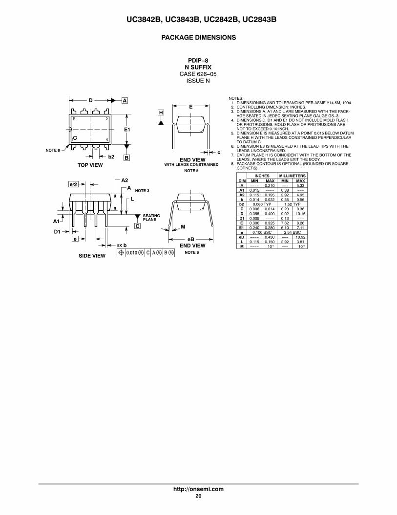
PACKAGE DIMENSIONS
PDIP−8N SUFFIX
CASE 626−05ISSUE N
1 4
58
b2NOTE 8
D
b
L
A1
A
eB
EA
TOP VIEW
C
SEATINGPLANE
0.010 C ASIDE VIEW
END VIEW
END VIEW
WITH LEADS CONSTRAINED
DIM MIN MAXINCHES
A −−−− 0.210A1 0.015 −−−−
b 0.014 0.022
C 0.008 0.014D 0.355 0.400D1 0.005 −−−−
e 0.100 BSC
E 0.300 0.325
M −−−− 10
−−− 5.330.38 −−−
0.35 0.56
0.20 0.369.02 10.160.13 −−−
2.54 BSC
7.62 8.26
−−− 10
MIN MAXMILLIMETERS
NOTES:1. DIMENSIONING AND TOLERANCING PER ASME Y14.5M, 1994.2. CONTROLLING DIMENSION: INCHES.3. DIMENSIONS A, A1 AND L ARE MEASURED WITH THE PACK-
AGE SEATED IN JEDEC SEATING PLANE GAUGE GS−3.4. DIMENSIONS D, D1 AND E1 DO NOT INCLUDE MOLD FLASH
OR PROTRUSIONS. MOLD FLASH OR PROTRUSIONS ARENOT TO EXCEED 0.10 INCH.
5. DIMENSION E IS MEASURED AT A POINT 0.015 BELOW DATUMPLANE H WITH THE LEADS CONSTRAINED PERPENDICULARTO DATUM C.
6. DIMENSION E3 IS MEASURED AT THE LEAD TIPS WITH THELEADS UNCONSTRAINED.
7. DATUM PLANE H IS COINCIDENT WITH THE BOTTOM OF THELEADS, WHERE THE LEADS EXIT THE BODY.
8. PACKAGE CONTOUR IS OPTIONAL (ROUNDED OR SQUARECORNERS).
E1 0.240 0.280 6.10 7.11
b2
eB −−−− 0.430 −−− 10.92
0.060 TYP 1.52 TYP
E1
M
8X
c
D1
B
A2 0.115 0.195 2.92 4.95
L 0.115 0.150 2.92 3.81°°
H
NOTE 5
e
e/2A2
NOTE 3
M B M NOTE 6
M
UC3842B, UC3843B, UC2842B, UC2843B
http://onsemi.com21
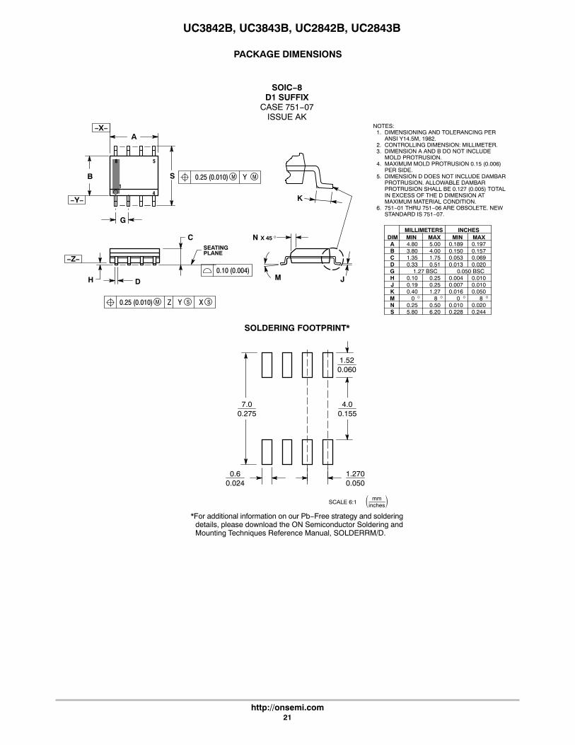
PACKAGE DIMENSIONS
SOIC−8D1 SUFFIX
CASE 751−07ISSUE AK
SEATINGPLANE
14
58
N
J
X 45�
K
NOTES:1. DIMENSIONING AND TOLERANCING PER
ANSI Y14.5M, 1982.2. CONTROLLING DIMENSION: MILLIMETER.3. DIMENSION A AND B DO NOT INCLUDE
MOLD PROTRUSION.4. MAXIMUM MOLD PROTRUSION 0.15 (0.006)
PER SIDE.5. DIMENSION D DOES NOT INCLUDE DAMBAR
PROTRUSION. ALLOWABLE DAMBARPROTRUSION SHALL BE 0.127 (0.005) TOTALIN EXCESS OF THE D DIMENSION ATMAXIMUM MATERIAL CONDITION.
6. 751−01 THRU 751−06 ARE OBSOLETE. NEWSTANDARD IS 751−07.
A
B S
DH
C
0.10 (0.004)
DIMA
MIN MAX MIN MAXINCHES
4.80 5.00 0.189 0.197
MILLIMETERS
B 3.80 4.00 0.150 0.157C 1.35 1.75 0.053 0.069D 0.33 0.51 0.013 0.020G 1.27 BSC 0.050 BSCH 0.10 0.25 0.004 0.010J 0.19 0.25 0.007 0.010K 0.40 1.27 0.016 0.050M 0 8 0 8 N 0.25 0.50 0.010 0.020S 5.80 6.20 0.228 0.244
−X−
−Y−
G
MYM0.25 (0.010)
−Z−
YM0.25 (0.010) Z S X S
M
� � � �
1.520.060
7.00.275
0.60.024
1.2700.050
4.00.155
� mminches
�SCALE 6:1
*For additional information on our Pb−Free strategy and solderingdetails, please download the ON Semiconductor Soldering andMounting Techniques Reference Manual, SOLDERRM/D.
SOLDERING FOOTPRINT*
UC3842B, UC3843B, UC2842B, UC2843B
http://onsemi.com22
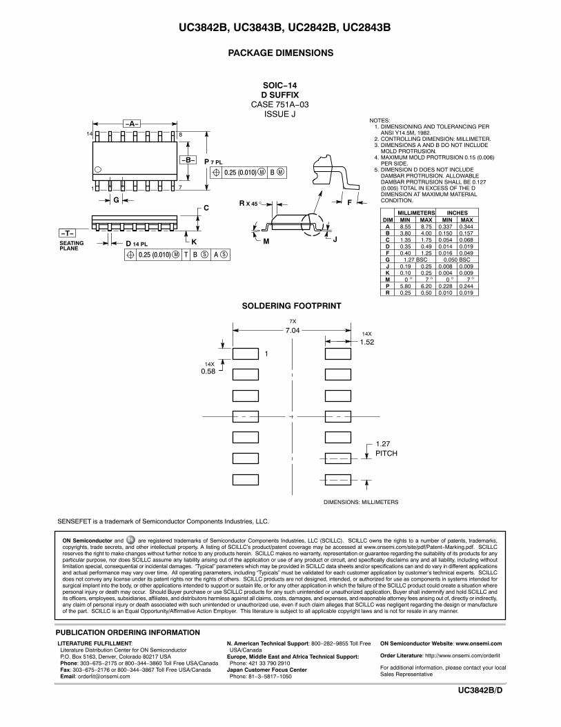
PACKAGE DIMENSIONS
SOIC−14D SUFFIX
CASE 751A−03ISSUE J
NOTES:1. DIMENSIONING AND TOLERANCING PER
ANSI Y14.5M, 1982.2. CONTROLLING DIMENSION: MILLIMETER.3. DIMENSIONS A AND B DO NOT INCLUDE
MOLD PROTRUSION.4. MAXIMUM MOLD PROTRUSION 0.15 (0.006)
PER SIDE.5. DIMENSION D DOES NOT INCLUDE
DAMBAR PROTRUSION. ALLOWABLEDAMBAR PROTRUSION SHALL BE 0.127(0.005) TOTAL IN EXCESS OF THE DDIMENSION AT MAXIMUM MATERIALCONDITION.
−A−
−B−
G
P 7 PL
14 8
71
M0.25 (0.010) B M
SBM0.25 (0.010) A ST
−T−
FR X 45
SEATINGPLANE
D 14 PL K
C
JM
�
DIM MIN MAX MIN MAXINCHESMILLIMETERS
A 8.55 8.75 0.337 0.344B 3.80 4.00 0.150 0.157C 1.35 1.75 0.054 0.068D 0.35 0.49 0.014 0.019F 0.40 1.25 0.016 0.049G 1.27 BSC 0.050 BSCJ 0.19 0.25 0.008 0.009K 0.10 0.25 0.004 0.009M 0 7 0 7 P 5.80 6.20 0.228 0.244R 0.25 0.50 0.010 0.019
� � � �
7.04
14X0.58
14X
1.52
1.27
DIMENSIONS: MILLIMETERS
1
PITCH
SOLDERING FOOTPRINT
7X
ON Semiconductor and are registered trademarks of Semiconductor Components Industries, LLC (SCILLC). SCILLC owns the rights to a number of patents, trademarks,copyrights, trade secrets, and other intellectual property. A listing of SCILLC’s product/patent coverage may be accessed at www.onsemi.com/site/pdf/Patent−Marking.pdf. SCILLCreserves the right to make changes without further notice to any products herein. SCILLC makes no warranty, representation or guarantee regarding the suitability of its products for anyparticular purpose, nor does SCILLC assume any liability arising out of the application or use of any product or circuit, and specifically disclaims any and all liability, including withoutlimitation special, consequential or incidental damages. “Typical” parameters which may be provided in SCILLC data sheets and/or specifications can and do vary in different applicationsand actual performance may vary over time. All operating parameters, including “Typicals” must be validated for each customer application by customer’s technical experts. SCILLCdoes not convey any license under its patent rights nor the rights of others. SCILLC products are not designed, intended, or authorized for use as components in systems intended forsurgical implant into the body, or other applications intended to support or sustain life, or for any other application in which the failure of the SCILLC product could create a situation wherepersonal injury or death may occur. Should Buyer purchase or use SCILLC products for any such unintended or unauthorized application, Buyer shall indemnify and hold SCILLC andits officers, employees, subsidiaries, affiliates, and distributors harmless against all claims, costs, damages, and expenses, and reasonable attorney fees arising out of, directly or indirectly,any claim of personal injury or death associated with such unintended or unauthorized use, even if such claim alleges that SCILLC was negligent regarding the design or manufactureof the part. SCILLC is an Equal Opportunity/Affirmative Action Employer. This literature is subject to all applicable copyright laws and is not for resale in any manner.
PUBLICATION ORDERING INFORMATIONN. American Technical Support: 800−282−9855 Toll FreeUSA/Canada
Europe, Middle East and Africa Technical Support:Phone: 421 33 790 2910
Japan Customer Focus CenterPhone: 81−3−5817−1050
UC3842B/D
SENSEFET is a trademark of Semiconductor Components Industries, LLC.
LITERATURE FULFILLMENT:Literature Distribution Center for ON SemiconductorP.O. Box 5163, Denver, Colorado 80217 USAPhone: 303−675−2175 or 800−344−3860 Toll Free USA/CanadaFax: 303−675−2176 or 800−344−3867 Toll Free USA/CanadaEmail: [email protected]
ON Semiconductor Website: www.onsemi.com
Order Literature: http://www.onsemi.com/orderlit
For additional information, please contact your localSales Representative