Embed Size (px)
Citation preview
UCS1002-1
Programmable USB Port Power Controller with Charger Emulation
DatasheetPRODUCT FEATURES
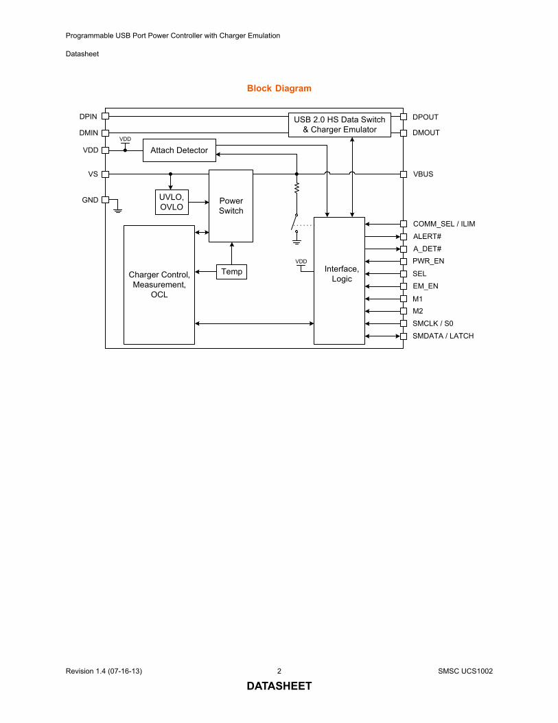
General DescriptionThe UCS1002 provides a USB port power switch forprecise control of up to 2.5 amperes continuous currentwith over-current l imit (OCL), dynamic thermalmanagement, latch or auto-recovery (low test current)fault handling, selectable active low or high enable,under- and over-voltage lockout, back-drive protection,and back-voltage protection. Split supply support for VS and VDD is an option for lowpower in system standby states. This gives batteryoperated applications, like notebook PCs, the ability todetect attachments from a sleep or off state. After theAttach Detection is flagged, the system can decide towake up and/or provide charging.In addition to power switching and current limitingmodes, the UCS1002 will automatically charge a widevariety of portable devices, including USB-IF BC1.2,YD/T-1591 (2009), most Apple® and RIM®, and manyothers. Nine preloaded charger emulation profilesmaximize compatibility coverage of peripheral devices.As well, a customizable charger emulation profile isavailable to accommodate unique existing and futureportable device handshaking / signature requirements.This custom profile uses a unique stimulus andresponse method referenced below.*The UCS1002 also provides current monitoring to allowintelligent management of system power and a BatteryFull option for controlled delivery of current regardlessof the host power state. This is especially important forbattery operated applications that want to provide powerin a standby and/or off state but do not want to drain thebattery excessively.The UCS1002 is available in a 20-pin QFN 4 mm x4 mm package.
Applications Notebook and Netbook Computers Tablets and E-book readers Desktops and Monitors Docking Stations and Printers AC-DC wall adapters
Features Port power switch with two current limit behaviors
— 2.9 V to 5.5 V source voltage range— Up to 2.5 A current with 55 mΩ On Resistance— Over-current trip or constant current limiting— Soft turn-on circuitry— Programmable current limit— Dynamic thermal management— Under- and over-voltage lockout— Back-drive, back-voltage protection— Latch or auto-recovery (low test current) fault handling— Selectable active high or low power switch enable— BC1.2 VBUS discharge port renegotiation function
Selectable / automatic cycling of USB data line charger emulation profiles— Customizable emulation profile uses a unique stimulus
and response method useful for future profiles*— Supports charger emulation— Allows for active cables— USB-IF BC1.2 charging downstream port (CDP) &
dedicated charging port (DCP) modes, YD/T-1591, and most Apple and RIM protocols standard; others as defined via the SMBus 2.0 / I2C®
— USB 2.0 compliant high-speed data switch (in Pass-through and CDP modes)
— Nine preloaded charger emulation profiles for maximum compatibility coverage of peripheral devices
— One custom programmable charger emulation profile for portable device support for fully host controlled charger emulation
Fault Alert open-drain output Self-contained current monitoring Low power Attach Detection and open-drain A_DET#
pin Ultra low power Sleep state Optional split supply support for VBUS and VDD for
low power in system standby states Wake on Attach USB SMBus 2.0 / I2C communications
— Supports Block Write and Read— Multiple SMBus addresses
Wide operating temperature range: -40 °C to +85 °C IEC61000-4-2 8 / 15 kV ESD immunity UL recognized and EN/IEC 60950-1 (CB) certified
* Unique technology covered under the following US patents pending: 13/109,446; 13/149,529; 13/173,287; 13/233,949; 13/157,282; 12/978,371; 13/232,965.
SMSC UCS1002 Revision 1.4 (07-16-13)
DATASHEET
Programmable USB Port Power Controller with Charger Emulation
Datasheet
Block Diagram
Charger Control, Measurement,
OCL
Interface, Logic
SMCLK / S0
SMDATA / LATCH
A_DET#
ALERT#
Power Switch
TempPWR_EN
DPOUT
DMOUT
DPIN
VDD
VS VBUS
DMIN
GND
USB 2.0 HS Data Switch & Charger Emulator
COMM_SEL / ILIM
Attach Detector
M1
M2
SEL
EM_EN
VDD
VDD
UVLO, OVLO
Revision 1.4 (07-16-13) 2 SMSC UCS1002
DATASHEET
Programmable USB Port Power Controller with Charger Emulation
Datasheet
SM
Cop
Circconsresebeforightversknowdesidamthis trad
The
SMSFITNOF DAMTORTO
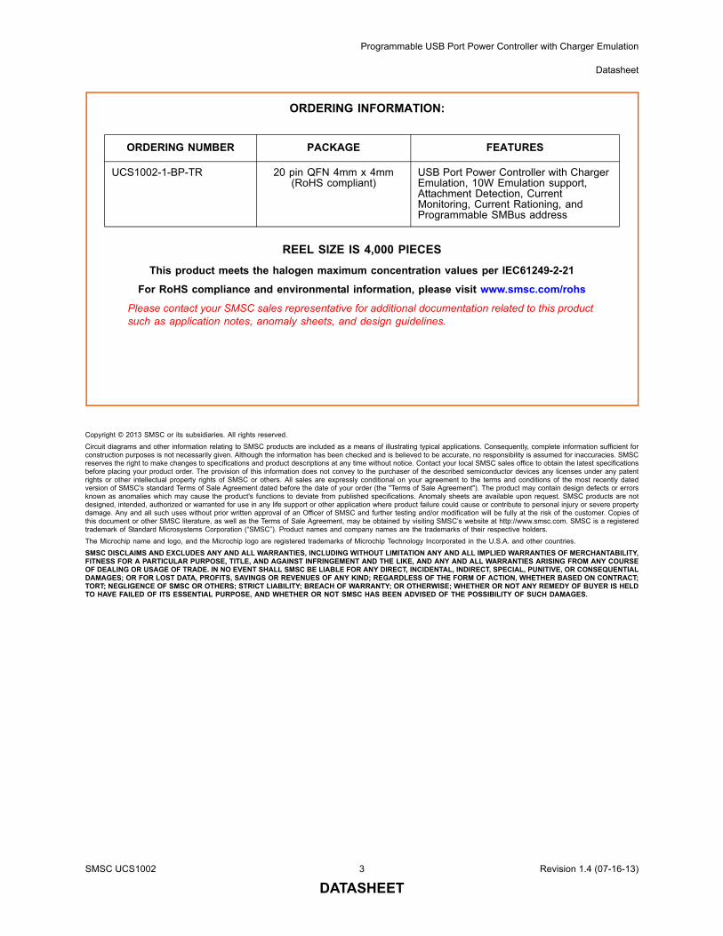
ORDERING INFORMATION:
SC UCS1002 3 Revision 1.4 (07-16-13)
DATASHEET
REEL SIZE IS 4,000 PIECES
This product meets the halogen maximum concentration values per IEC61249-2-21
For RoHS compliance and environmental information, please visit www.smsc.com/rohs
Please contact your SMSC sales representative for additional documentation related to this product such as application notes, anomaly sheets, and design guidelines.
ORDERING NUMBER PACKAGE FEATURES
UCS1002-1-BP-TR 20 pin QFN 4mm x 4mm(RoHS compliant)
USB Port Power Controller with Charger Emulation, 10W Emulation support, Attachment Detection, Current Monitoring, Current Rationing, and Programmable SMBus address
yright © 2013 SMSC or its subsidiaries. All rights reserved.
uit diagrams and other information relating to SMSC products are included as a means of illustrating typical applications. Consequently, complete information sufficient fortruction purposes is not necessarily given. Although the information has been checked and is believed to be accurate, no responsibility is assumed for inaccuracies. SMSCrves the right to make changes to specifications and product descriptions at any time without notice. Contact your local SMSC sales office to obtain the latest specificationsre placing your product order. The provision of this information does not convey to the purchaser of the described semiconductor devices any licenses under any patents or other intellectual property rights of SMSC or others. All sales are expressly conditional on your agreement to the terms and conditions of the most recently datedion of SMSC's standard Terms of Sale Agreement dated before the date of your order (the "Terms of Sale Agreement"). The product may contain design defects or errorsn as anomalies which may cause the product's functions to deviate from published specifications. Anomaly sheets are available upon request. SMSC products are not
gned, intended, authorized or warranted for use in any life support or other application where product failure could cause or contribute to personal injury or severe propertyage. Any and all such uses without prior written approval of an Officer of SMSC and further testing and/or modification will be fully at the risk of the customer. Copies ofdocument or other SMSC literature, as well as the Terms of Sale Agreement, may be obtained by visiting SMSC’s website at http://www.smsc.com. SMSC is a registeredemark of Standard Microsystems Corporation (“SMSC”). Product names and company names are the trademarks of their respective holders.
Microchip name and logo, and the Microchip logo are registered trademarks of Microchip Technology Incorporated in the U.S.A. and other countries.
C DISCLAIMS AND EXCLUDES ANY AND ALL WARRANTIES, INCLUDING WITHOUT LIMITATION ANY AND ALL IMPLIED WARRANTIES OF MERCHANTABILITY,ESS FOR A PARTICULAR PURPOSE, TITLE, AND AGAINST INFRINGEMENT AND THE LIKE, AND ANY AND ALL WARRANTIES ARISING FROM ANY COURSE
DEALING OR USAGE OF TRADE. IN NO EVENT SHALL SMSC BE LIABLE FOR ANY DIRECT, INCIDENTAL, INDIRECT, SPECIAL, PUNITIVE, OR CONSEQUENTIALAGES; OR FOR LOST DATA, PROFITS, SAVINGS OR REVENUES OF ANY KIND; REGARDLESS OF THE FORM OF ACTION, WHETHER BASED ON CONTRACT;T; NEGLIGENCE OF SMSC OR OTHERS; STRICT LIABILITY; BREACH OF WARRANTY; OR OTHERWISE; WHETHER OR NOT ANY REMEDY OF BUYER IS HELD
HAVE FAILED OF ITS ESSENTIAL PURPOSE, AND WHETHER OR NOT SMSC HAS BEEN ADVISED OF THE POSSIBILITY OF SUCH DAMAGES.
Programmable USB Port Power Controller with Charger Emulation
Datasheet
Table of Contents
Chapter 1 Terms and Abbreviations . . . . . . . . . . . . . . . . . . . . . . . . . . . . . . . . . . . . . . . . . . . . 10
Chapter 2 Pin Description . . . . . . . . . . . . . . . . . . . . . . . . . . . . . . . . . . . . . . . . . . . . . . . . . . . . . 12
Chapter 3 Electrical Specifications . . . . . . . . . . . . . . . . . . . . . . . . . . . . . . . . . . . . . . . . . . . . . . 153.1 ESD & Transient Performance . . . . . . . . . . . . . . . . . . . . . . . . . . . . . . . . . . . . . . . . . . . . . . . . . . . . . . 26
3.1.1 Human Body Model (HBM) Performance . . . . . . . . . . . . . . . . . . . . . . . . . . . . . . . . . . . . . . . 263.1.2 Charged Device Model (CDM) Performance . . . . . . . . . . . . . . . . . . . . . . . . . . . . . . . . . . . . . 263.1.3 IEC61000-4-2 Performance. . . . . . . . . . . . . . . . . . . . . . . . . . . . . . . . . . . . . . . . . . . . . . . . . . 26
Chapter 4 Communications . . . . . . . . . . . . . . . . . . . . . . . . . . . . . . . . . . . . . . . . . . . . . . . . . . . . 274.1 Operating Mode. . . . . . . . . . . . . . . . . . . . . . . . . . . . . . . . . . . . . . . . . . . . . . . . . . . . . . . . . . . . . . . . . . 274.2 SMBus Operating Mode . . . . . . . . . . . . . . . . . . . . . . . . . . . . . . . . . . . . . . . . . . . . . . . . . . . . . . . . . . . 28
4.2.1 System Management Bus . . . . . . . . . . . . . . . . . . . . . . . . . . . . . . . . . . . . . . . . . . . . . . . . . . . 284.2.2 SMBus and I2C Compatibility . . . . . . . . . . . . . . . . . . . . . . . . . . . . . . . . . . . . . . . . . . . . . . . . 304.2.3 SMBus Protocols . . . . . . . . . . . . . . . . . . . . . . . . . . . . . . . . . . . . . . . . . . . . . . . . . . . . . . . . . . 304.2.4 I2C Protocols . . . . . . . . . . . . . . . . . . . . . . . . . . . . . . . . . . . . . . . . . . . . . . . . . . . . . . . . . . . . . 31
4.3 Stand-alone Operating Mode . . . . . . . . . . . . . . . . . . . . . . . . . . . . . . . . . . . . . . . . . . . . . . . . . . . . . . . 32
Chapter 5 General Description . . . . . . . . . . . . . . . . . . . . . . . . . . . . . . . . . . . . . . . . . . . . . . . . . 345.1 UCS1002 Power States. . . . . . . . . . . . . . . . . . . . . . . . . . . . . . . . . . . . . . . . . . . . . . . . . . . . . . . . . . . . 38
5.1.1 Off State Operation . . . . . . . . . . . . . . . . . . . . . . . . . . . . . . . . . . . . . . . . . . . . . . . . . . . . . . . . 395.1.2 Sleep State Operation . . . . . . . . . . . . . . . . . . . . . . . . . . . . . . . . . . . . . . . . . . . . . . . . . . . . . . 405.1.3 Detect State Operation . . . . . . . . . . . . . . . . . . . . . . . . . . . . . . . . . . . . . . . . . . . . . . . . . . . . . 415.1.4 Active State Operation. . . . . . . . . . . . . . . . . . . . . . . . . . . . . . . . . . . . . . . . . . . . . . . . . . . . . . 425.1.5 Error State Operation. . . . . . . . . . . . . . . . . . . . . . . . . . . . . . . . . . . . . . . . . . . . . . . . . . . . . . . 43
5.2 Supply Voltages. . . . . . . . . . . . . . . . . . . . . . . . . . . . . . . . . . . . . . . . . . . . . . . . . . . . . . . . . . . . . . . . . . 435.2.1 VDD Supply Voltage . . . . . . . . . . . . . . . . . . . . . . . . . . . . . . . . . . . . . . . . . . . . . . . . . . . . . . . 435.2.2 VS Source Voltage . . . . . . . . . . . . . . . . . . . . . . . . . . . . . . . . . . . . . . . . . . . . . . . . . . . . . . . . 435.2.3 Back-voltage Detection . . . . . . . . . . . . . . . . . . . . . . . . . . . . . . . . . . . . . . . . . . . . . . . . . . . . . 445.2.4 Back-drive Current Protection . . . . . . . . . . . . . . . . . . . . . . . . . . . . . . . . . . . . . . . . . . . . . . . . 445.2.5 Under-voltage Lockout on VS . . . . . . . . . . . . . . . . . . . . . . . . . . . . . . . . . . . . . . . . . . . . . . . . 445.2.6 Over-voltage Detection and Lockout on VS. . . . . . . . . . . . . . . . . . . . . . . . . . . . . . . . . . . . . . 44
5.3 Discrete Input Pins . . . . . . . . . . . . . . . . . . . . . . . . . . . . . . . . . . . . . . . . . . . . . . . . . . . . . . . . . . . . . . . 445.3.1 COMM_SEL / ILIM Input . . . . . . . . . . . . . . . . . . . . . . . . . . . . . . . . . . . . . . . . . . . . . . . . . . . . 445.3.2 SEL Input . . . . . . . . . . . . . . . . . . . . . . . . . . . . . . . . . . . . . . . . . . . . . . . . . . . . . . . . . . . . . . . . 445.3.3 M1, M2, and EM_EN Inputs. . . . . . . . . . . . . . . . . . . . . . . . . . . . . . . . . . . . . . . . . . . . . . . . . . 455.3.4 PWR_EN Input . . . . . . . . . . . . . . . . . . . . . . . . . . . . . . . . . . . . . . . . . . . . . . . . . . . . . . . . . . . 455.3.5 Latch Input . . . . . . . . . . . . . . . . . . . . . . . . . . . . . . . . . . . . . . . . . . . . . . . . . . . . . . . . . . . . . . . 455.3.6 S0 Input . . . . . . . . . . . . . . . . . . . . . . . . . . . . . . . . . . . . . . . . . . . . . . . . . . . . . . . . . . . . . . . . . 45
5.4 Discrete Output Pins . . . . . . . . . . . . . . . . . . . . . . . . . . . . . . . . . . . . . . . . . . . . . . . . . . . . . . . . . . . . . . 455.4.1 ALERT# and A_DET# Output Pins . . . . . . . . . . . . . . . . . . . . . . . . . . . . . . . . . . . . . . . . . . . . 455.4.2 Interrupt Blanking. . . . . . . . . . . . . . . . . . . . . . . . . . . . . . . . . . . . . . . . . . . . . . . . . . . . . . . . . . 46
Chapter 6 USB High-speed Data Switch . . . . . . . . . . . . . . . . . . . . . . . . . . . . . . . . . . . . . . . . . 476.1 USB High-speed Data Switch . . . . . . . . . . . . . . . . . . . . . . . . . . . . . . . . . . . . . . . . . . . . . . . . . . . . . . . 47
6.1.1 USB-IF High-speed Compliance . . . . . . . . . . . . . . . . . . . . . . . . . . . . . . . . . . . . . . . . . . . . . . 47
Revision 1.4 (07-16-13) 4 SMSC UCS1002
DATASHEET
Programmable USB Port Power Controller with Charger Emulation
Datasheet
Chapter 7 USB Port Power Switch . . . . . . . . . . . . . . . . . . . . . . . . . . . . . . . . . . . . . . . . . . . . . . 487.1 USB Port Power Switch. . . . . . . . . . . . . . . . . . . . . . . . . . . . . . . . . . . . . . . . . . . . . . . . . . . . . . . . . . . . 487.2 Current Limiting . . . . . . . . . . . . . . . . . . . . . . . . . . . . . . . . . . . . . . . . . . . . . . . . . . . . . . . . . . . . . . . . . . 48
7.2.1 Current Limit Setting . . . . . . . . . . . . . . . . . . . . . . . . . . . . . . . . . . . . . . . . . . . . . . . . . . . . . . . 487.2.2 Short Circuit Output Current Limiting. . . . . . . . . . . . . . . . . . . . . . . . . . . . . . . . . . . . . . . . . . . 487.2.3 Soft Start . . . . . . . . . . . . . . . . . . . . . . . . . . . . . . . . . . . . . . . . . . . . . . . . . . . . . . . . . . . . . . . . 487.2.4 Current Limiting Modes . . . . . . . . . . . . . . . . . . . . . . . . . . . . . . . . . . . . . . . . . . . . . . . . . . . . . 48
7.3 Thermal Management and Voltage Protection . . . . . . . . . . . . . . . . . . . . . . . . . . . . . . . . . . . . . . . . . . 517.3.1 Thermal Management . . . . . . . . . . . . . . . . . . . . . . . . . . . . . . . . . . . . . . . . . . . . . . . . . . . . . . 51
7.4 VBUS Discharge . . . . . . . . . . . . . . . . . . . . . . . . . . . . . . . . . . . . . . . . . . . . . . . . . . . . . . . . . . . . . . . . . 537.5 Battery Full . . . . . . . . . . . . . . . . . . . . . . . . . . . . . . . . . . . . . . . . . . . . . . . . . . . . . . . . . . . . . . . . . . . . . 53
7.5.1 Charge Rationing Interactions . . . . . . . . . . . . . . . . . . . . . . . . . . . . . . . . . . . . . . . . . . . . . . . . 557.6 Fault Handling Mechanism . . . . . . . . . . . . . . . . . . . . . . . . . . . . . . . . . . . . . . . . . . . . . . . . . . . . . . . . . 56
7.6.1 Auto-recovery Fault Handling . . . . . . . . . . . . . . . . . . . . . . . . . . . . . . . . . . . . . . . . . . . . . . . . 577.6.2 Latched Fault Handling . . . . . . . . . . . . . . . . . . . . . . . . . . . . . . . . . . . . . . . . . . . . . . . . . . . . . 57
Chapter 8 Detect State . . . . . . . . . . . . . . . . . . . . . . . . . . . . . . . . . . . . . . . . . . . . . . . . . . . . . . . . 588.1 Device Attach / Removal Detection . . . . . . . . . . . . . . . . . . . . . . . . . . . . . . . . . . . . . . . . . . . . . . . . . . . 588.2 VBUS Bypass Switch . . . . . . . . . . . . . . . . . . . . . . . . . . . . . . . . . . . . . . . . . . . . . . . . . . . . . . . . . . . . . 588.3 Attach Detection . . . . . . . . . . . . . . . . . . . . . . . . . . . . . . . . . . . . . . . . . . . . . . . . . . . . . . . . . . . . . . . . . 588.4 Removal Detection . . . . . . . . . . . . . . . . . . . . . . . . . . . . . . . . . . . . . . . . . . . . . . . . . . . . . . . . . . . . . . . 58
Chapter 9 Active State . . . . . . . . . . . . . . . . . . . . . . . . . . . . . . . . . . . . . . . . . . . . . . . . . . . . . . . . 609.1 Active State Overview . . . . . . . . . . . . . . . . . . . . . . . . . . . . . . . . . . . . . . . . . . . . . . . . . . . . . . . . . . . . . 609.2 Active Mode Selection . . . . . . . . . . . . . . . . . . . . . . . . . . . . . . . . . . . . . . . . . . . . . . . . . . . . . . . . . . . . . 609.3 BC1.2 Detection Renegotiation . . . . . . . . . . . . . . . . . . . . . . . . . . . . . . . . . . . . . . . . . . . . . . . . . . . . . . 609.4 Data Pass-through (No Charger Emulation) . . . . . . . . . . . . . . . . . . . . . . . . . . . . . . . . . . . . . . . . . . . . 609.5 BC1.2 SDP (No Charger Emulation) . . . . . . . . . . . . . . . . . . . . . . . . . . . . . . . . . . . . . . . . . . . . . . . . . . 619.6 BC1.2 CDP . . . . . . . . . . . . . . . . . . . . . . . . . . . . . . . . . . . . . . . . . . . . . . . . . . . . . . . . . . . . . . . . . . . . . 61
9.6.1 BC1.2 CDP Charger Emulation Profile . . . . . . . . . . . . . . . . . . . . . . . . . . . . . . . . . . . . . . . . . 619.7 BC1.2 DCP . . . . . . . . . . . . . . . . . . . . . . . . . . . . . . . . . . . . . . . . . . . . . . . . . . . . . . . . . . . . . . . . . . . . . 62
9.7.1 BC1.2 DCP Charger Emulation Profile . . . . . . . . . . . . . . . . . . . . . . . . . . . . . . . . . . . . . . . . . 629.8 Dedicated Charger . . . . . . . . . . . . . . . . . . . . . . . . . . . . . . . . . . . . . . . . . . . . . . . . . . . . . . . . . . . . . . . 62
9.8.1 Emulation Reset . . . . . . . . . . . . . . . . . . . . . . . . . . . . . . . . . . . . . . . . . . . . . . . . . . . . . . . . . . 629.8.2 Emulation Cycling . . . . . . . . . . . . . . . . . . . . . . . . . . . . . . . . . . . . . . . . . . . . . . . . . . . . . . . . . 639.8.3 DCE Cycle Retry . . . . . . . . . . . . . . . . . . . . . . . . . . . . . . . . . . . . . . . . . . . . . . . . . . . . . . . . . . 63
9.9 Current Limit Mode Associations. . . . . . . . . . . . . . . . . . . . . . . . . . . . . . . . . . . . . . . . . . . . . . . . . . . . . 649.10 No Handshake. . . . . . . . . . . . . . . . . . . . . . . . . . . . . . . . . . . . . . . . . . . . . . . . . . . . . . . . . . . . . . . . . . 649.11 Preloaded Charger Emulation Profiles . . . . . . . . . . . . . . . . . . . . . . . . . . . . . . . . . . . . . . . . . . . . . . . 65
9.11.1 BC1.2 DCP Charger Emulation Profile Within DCE Cycle . . . . . . . . . . . . . . . . . . . . . . . . . 659.11.2 Legacy 2 Charger Emulation Profile . . . . . . . . . . . . . . . . . . . . . . . . . . . . . . . . . . . . . . . . . . 659.11.3 Legacy 1, 3, 4, and 6 Charger Emulation Profiles . . . . . . . . . . . . . . . . . . . . . . . . . . . . . . . . 669.11.4 Legacy 5 Charger Emulation Profile . . . . . . . . . . . . . . . . . . . . . . . . . . . . . . . . . . . . . . . . . . 669.11.5 Legacy 7 Charger Emulation Profile . . . . . . . . . . . . . . . . . . . . . . . . . . . . . . . . . . . . . . . . . . 66
9.12 Custom Charger Emulation Profile . . . . . . . . . . . . . . . . . . . . . . . . . . . . . . . . . . . . . . . . . . . . . . . . . . 67
Chapter 10 Register Description . . . . . . . . . . . . . . . . . . . . . . . . . . . . . . . . . . . . . . . . . . . . . . . . 6810.1 Current Measurement Register . . . . . . . . . . . . . . . . . . . . . . . . . . . . . . . . . . . . . . . . . . . . . . . . . . . . . 7110.2 Total Accumulated Charge Registers . . . . . . . . . . . . . . . . . . . . . . . . . . . . . . . . . . . . . . . . . . . . . . . . 7210.3 Status Registers . . . . . . . . . . . . . . . . . . . . . . . . . . . . . . . . . . . . . . . . . . . . . . . . . . . . . . . . . . . . . . . . 73
SMSC UCS1002 5 Revision 1.4 (07-16-13)
DATASHEET
Programmable USB Port Power Controller with Charger Emulation
Datasheet
10.3.1 Other Status - 0Fh . . . . . . . . . . . . . . . . . . . . . . . . . . . . . . . . . . . . . . . . . . . . . . . . . . . . . . . . 7310.3.2 Interrupt Status - 10h . . . . . . . . . . . . . . . . . . . . . . . . . . . . . . . . . . . . . . . . . . . . . . . . . . . . . . 7410.3.3 General Status - 11h . . . . . . . . . . . . . . . . . . . . . . . . . . . . . . . . . . . . . . . . . . . . . . . . . . . . . . 7510.3.4 Profile Status 1 - 12h . . . . . . . . . . . . . . . . . . . . . . . . . . . . . . . . . . . . . . . . . . . . . . . . . . . . . . 7510.3.5 Profile Status 2 - 13h . . . . . . . . . . . . . . . . . . . . . . . . . . . . . . . . . . . . . . . . . . . . . . . . . . . . . . 7610.3.6 Pin Status Register - 14h. . . . . . . . . . . . . . . . . . . . . . . . . . . . . . . . . . . . . . . . . . . . . . . . . . . 77
10.4 Configuration Registers . . . . . . . . . . . . . . . . . . . . . . . . . . . . . . . . . . . . . . . . . . . . . . . . . . . . . . . . . . . 7810.4.1 General Configuration - 15h . . . . . . . . . . . . . . . . . . . . . . . . . . . . . . . . . . . . . . . . . . . . . . . . 7810.4.2 Emulation Configuration - 16h . . . . . . . . . . . . . . . . . . . . . . . . . . . . . . . . . . . . . . . . . . . . . . . 7910.4.3 Switch Configuration - 17h. . . . . . . . . . . . . . . . . . . . . . . . . . . . . . . . . . . . . . . . . . . . . . . . . . 8010.4.4 Attach Detection Configuration - 18h. . . . . . . . . . . . . . . . . . . . . . . . . . . . . . . . . . . . . . . . . . 8110.4.5 High-speed Switch Configuration - 25h . . . . . . . . . . . . . . . . . . . . . . . . . . . . . . . . . . . . . . . . 82
10.5 Current Limit Register . . . . . . . . . . . . . . . . . . . . . . . . . . . . . . . . . . . . . . . . . . . . . . . . . . . . . . . . . . . . 8210.6 Charge Rationing Threshold Registers . . . . . . . . . . . . . . . . . . . . . . . . . . . . . . . . . . . . . . . . . . . . . . . 8310.7 Auto-recovery Configuration Register . . . . . . . . . . . . . . . . . . . . . . . . . . . . . . . . . . . . . . . . . . . . . . . . 8410.8 IBUS_CHG Configuration Register . . . . . . . . . . . . . . . . . . . . . . . . . . . . . . . . . . . . . . . . . . . . . . . . . . 8510.9 tDET_CHARGE Configuration Register . . . . . . . . . . . . . . . . . . . . . . . . . . . . . . . . . . . . . . . . . . . . . . 8510.10 Preloaded Emulation Enable Registers. . . . . . . . . . . . . . . . . . . . . . . . . . . . . . . . . . . . . . . . . . . . . . 87
10.10.1 BCS Emulation Enable - 20h . . . . . . . . . . . . . . . . . . . . . . . . . . . . . . . . . . . . . . . . . . . . . . . 8710.10.2 Legacy Emulation Enable - 21h. . . . . . . . . . . . . . . . . . . . . . . . . . . . . . . . . . . . . . . . . . . . . 87
10.11 Preloaded Emulation Timeout Configuration Registers. . . . . . . . . . . . . . . . . . . . . . . . . . . . . . . . . . 8810.11.1 BCS Emulation Timeout Config - 22h . . . . . . . . . . . . . . . . . . . . . . . . . . . . . . . . . . . . . . . . 8810.11.2 Legacy Emulation Timeout Config 1 - 23h. . . . . . . . . . . . . . . . . . . . . . . . . . . . . . . . . . . . . 8910.11.3 Legacy Emulation Timeout Config 2 - 24h. . . . . . . . . . . . . . . . . . . . . . . . . . . . . . . . . . . . . 89
10.12 Preloaded Emulation Configuration Registers. . . . . . . . . . . . . . . . . . . . . . . . . . . . . . . . . . . . . . . . . 9010.12.1 Applied Charger Emulation - 30h. . . . . . . . . . . . . . . . . . . . . . . . . . . . . . . . . . . . . . . . . . . . 9110.12.2 Preloaded Emulation Configuration Registers 31h - 3Bh . . . . . . . . . . . . . . . . . . . . . . . . . 9110.12.3 Preloaded Emulation Stimulus X - Config 1 - 31h, 35h, 39h . . . . . . . . . . . . . . . . . . . . . . . 9210.12.4 BC1.2 Emulation Stimulus X - Config 2 - 32h, 36h, 3Ah . . . . . . . . . . . . . . . . . . . . . . . . . . 9310.12.5 Emulation Stimulus X - Config 3 - 33h, 37h, 3Bh . . . . . . . . . . . . . . . . . . . . . . . . . . . . . . . 9710.12.6 Emulation Stimulus X - Config 4 - 34h, 38h. . . . . . . . . . . . . . . . . . . . . . . . . . . . . . . . . . . . 98
10.13 Custom Emulation Configuration Registers. . . . . . . . . . . . . . . . . . . . . . . . . . . . . . . . . . . . . . . . . . . 9910.13.1 Custom Emulation Configuration - 40h . . . . . . . . . . . . . . . . . . . . . . . . . . . . . . . . . . . . . . 10010.13.2 Custom Stimulus / Response Pair X - Config 1 - 41h, 45h, 49h . . . . . . . . . . . . . . . . . . . 10110.13.3 Custom Stimulus / Response Pair X - Config 2 - 42h, 46h, 4Ah . . . . . . . . . . . . . . . . . . . 10110.13.4 Custom Stimulus / Response Pair X - Config 3 - 43h, 47h, 4Bh . . . . . . . . . . . . . . . . . . . 10110.13.5 Custom Stimulus / Response Pair X - Config 4 - 44h, 48h, 4Ch . . . . . . . . . . . . . . . . . . . 102
10.14 Current Limiting Behavior Configuration Registers . . . . . . . . . . . . . . . . . . . . . . . . . . . . . . . . . . . . 10210.14.1 Applied Current Limiting Behavior - 50h . . . . . . . . . . . . . . . . . . . . . . . . . . . . . . . . . . . . . 10210.14.2 Custom Current Limiting Behavior Configuration - 51h . . . . . . . . . . . . . . . . . . . . . . . . . . 102
10.15 Product ID Register . . . . . . . . . . . . . . . . . . . . . . . . . . . . . . . . . . . . . . . . . . . . . . . . . . . . . . . . . . . . 10310.16 Manufacturer ID Register . . . . . . . . . . . . . . . . . . . . . . . . . . . . . . . . . . . . . . . . . . . . . . . . . . . . . . . 10410.17 Revision Register . . . . . . . . . . . . . . . . . . . . . . . . . . . . . . . . . . . . . . . . . . . . . . . . . . . . . . . . . . . . . 104
Chapter 11 Package Information . . . . . . . . . . . . . . . . . . . . . . . . . . . . . . . . . . . . . . . . . . . . . . 105
Chapter 12 Typical Operating Curves . . . . . . . . . . . . . . . . . . . . . . . . . . . . . . . . . . . . . . . . . . 107
Chapter 13 References . . . . . . . . . . . . . . . . . . . . . . . . . . . . . . . . . . . . . . . . . . . . . . . . . . . . . . . 111
Chapter 14 Document Revision History . . . . . . . . . . . . . . . . . . . . . . . . . . . . . . . . . . . . . . . . . 112
Revision 1.4 (07-16-13) 6 SMSC UCS1002
DATASHEET
Programmable USB Port Power Controller with Charger Emulation
Datasheet
List of Tables
Table 1.1 Terms and Abbreviations. . . . . . . . . . . . . . . . . . . . . . . . . . . . . . . . . . . . . . . . . . . . . . . . . . . . . 10Table 2.1 UCS1002 Pin Description . . . . . . . . . . . . . . . . . . . . . . . . . . . . . . . . . . . . . . . . . . . . . . . . . . . . 12Table 2.2 Pin Types. . . . . . . . . . . . . . . . . . . . . . . . . . . . . . . . . . . . . . . . . . . . . . . . . . . . . . . . . . . . . . . . . 14Table 3.1 Absolute Maximum Ratings . . . . . . . . . . . . . . . . . . . . . . . . . . . . . . . . . . . . . . . . . . . . . . . . . . . 15Table 3.2 Power Dissipation Summary . . . . . . . . . . . . . . . . . . . . . . . . . . . . . . . . . . . . . . . . . . . . . . . . . . 15Table 3.3 Electrical Specifications . . . . . . . . . . . . . . . . . . . . . . . . . . . . . . . . . . . . . . . . . . . . . . . . . . . . . . 16Table 3.4 ESD Ratings . . . . . . . . . . . . . . . . . . . . . . . . . . . . . . . . . . . . . . . . . . . . . . . . . . . . . . . . . . . . . . 26Table 4.1 UCS1002 Communication Mode and ILIM Selection . . . . . . . . . . . . . . . . . . . . . . . . . . . . . . . 27Table 4.2 SEL Pin Decode . . . . . . . . . . . . . . . . . . . . . . . . . . . . . . . . . . . . . . . . . . . . . . . . . . . . . . . . . . . 29Table 4.3 Protocol Format . . . . . . . . . . . . . . . . . . . . . . . . . . . . . . . . . . . . . . . . . . . . . . . . . . . . . . . . . . . . 30Table 4.4 Write Byte Protocol . . . . . . . . . . . . . . . . . . . . . . . . . . . . . . . . . . . . . . . . . . . . . . . . . . . . . . . . . 31Table 4.5 Read Byte Protocol . . . . . . . . . . . . . . . . . . . . . . . . . . . . . . . . . . . . . . . . . . . . . . . . . . . . . . . . . 31Table 4.6 Send Byte Protocol . . . . . . . . . . . . . . . . . . . . . . . . . . . . . . . . . . . . . . . . . . . . . . . . . . . . . . . . . 31Table 4.7 Receive Byte Protocol . . . . . . . . . . . . . . . . . . . . . . . . . . . . . . . . . . . . . . . . . . . . . . . . . . . . . . . 31Table 4.8 Block Write Protocol . . . . . . . . . . . . . . . . . . . . . . . . . . . . . . . . . . . . . . . . . . . . . . . . . . . . . . . . 32Table 4.9 Block Read Protocol . . . . . . . . . . . . . . . . . . . . . . . . . . . . . . . . . . . . . . . . . . . . . . . . . . . . . . . . 32Table 4.10 Stand-alone Fault and Attach Detection Selection . . . . . . . . . . . . . . . . . . . . . . . . . . . . . . . . . 33Table 5.1 Power States Control Settings. . . . . . . . . . . . . . . . . . . . . . . . . . . . . . . . . . . . . . . . . . . . . . . . . 39Table 7.1 Charge Rationing Behavior . . . . . . . . . . . . . . . . . . . . . . . . . . . . . . . . . . . . . . . . . . . . . . . . . . . 54Table 7.2 Charge Rationing Reset Behavior . . . . . . . . . . . . . . . . . . . . . . . . . . . . . . . . . . . . . . . . . . . . . . 54Table 7.3 Effects of Changing Rationing Behavior after Threshold Reached . . . . . . . . . . . . . . . . . . . . . 55Table 9.1 Active Mode Selection . . . . . . . . . . . . . . . . . . . . . . . . . . . . . . . . . . . . . . . . . . . . . . . . . . . . . . . 60Table 9.2 Current Limit Mode Options. . . . . . . . . . . . . . . . . . . . . . . . . . . . . . . . . . . . . . . . . . . . . . . . . . . 64Table 10.1 Register Set in Hexadecimal Order . . . . . . . . . . . . . . . . . . . . . . . . . . . . . . . . . . . . . . . . . . . . . 68Table 10.2 Current Measurement Register . . . . . . . . . . . . . . . . . . . . . . . . . . . . . . . . . . . . . . . . . . . . . . . . 71Table 10.3 Total Accumulated Charge Registers . . . . . . . . . . . . . . . . . . . . . . . . . . . . . . . . . . . . . . . . . . . 72Table 10.4 Status Registers . . . . . . . . . . . . . . . . . . . . . . . . . . . . . . . . . . . . . . . . . . . . . . . . . . . . . . . . . . . 73Table 10.5 EM_STEP Bit Decode . . . . . . . . . . . . . . . . . . . . . . . . . . . . . . . . . . . . . . . . . . . . . . . . . . . . . . . 74Table 10.6 PWR_STATE Bit Decode . . . . . . . . . . . . . . . . . . . . . . . . . . . . . . . . . . . . . . . . . . . . . . . . . . . . 77Table 10.7 Configuration Registers . . . . . . . . . . . . . . . . . . . . . . . . . . . . . . . . . . . . . . . . . . . . . . . . . . . . . . 78Table 10.8 EM_RESET_TIME Bit Decode . . . . . . . . . . . . . . . . . . . . . . . . . . . . . . . . . . . . . . . . . . . . . . . . 80Table 10.9 Discharge Time Options . . . . . . . . . . . . . . . . . . . . . . . . . . . . . . . . . . . . . . . . . . . . . . . . . . . . . 81Table 10.10Attach / Removal Detection Threshold Options . . . . . . . . . . . . . . . . . . . . . . . . . . . . . . . . . . . 81Table 10.11Current Limit Register. . . . . . . . . . . . . . . . . . . . . . . . . . . . . . . . . . . . . . . . . . . . . . . . . . . . . . . 82Table 10.12ILIM_SW Bit Decode . . . . . . . . . . . . . . . . . . . . . . . . . . . . . . . . . . . . . . . . . . . . . . . . . . . . . . . 83Table 10.13Charge Rationing Threshold Registers . . . . . . . . . . . . . . . . . . . . . . . . . . . . . . . . . . . . . . . . . 83Table 10.14Auto-recovery Configuration Register . . . . . . . . . . . . . . . . . . . . . . . . . . . . . . . . . . . . . . . . . . 84Table 10.15tCYCLE Options . . . . . . . . . . . . . . . . . . . . . . . . . . . . . . . . . . . . . . . . . . . . . . . . . . . . . . . . . . . . 84Table 10.16TRST_SW Options . . . . . . . . . . . . . . . . . . . . . . . . . . . . . . . . . . . . . . . . . . . . . . . . . . . . . . . . . 84Table 10.17VTST_SW Options . . . . . . . . . . . . . . . . . . . . . . . . . . . . . . . . . . . . . . . . . . . . . . . . . . . . . . . . . 85Table 10.18IBUS_CHG Configuration Register . . . . . . . . . . . . . . . . . . . . . . . . . . . . . . . . . . . . . . . . . . . . 85Table 10.19tDET_CHARGE Configuration Register . . . . . . . . . . . . . . . . . . . . . . . . . . . . . . . . . . . . . . . . . 85Table 10.20DC_TEMP_SET Bit Decode. . . . . . . . . . . . . . . . . . . . . . . . . . . . . . . . . . . . . . . . . . . . . . . . . . 86Table 10.21DET_CHARGE_SET Bit Decode . . . . . . . . . . . . . . . . . . . . . . . . . . . . . . . . . . . . . . . . . . . . . . 86Table 10.22Preloaded Emulation Enable Registers . . . . . . . . . . . . . . . . . . . . . . . . . . . . . . . . . . . . . . . . . 87Table 10.23Preloaded Emulation Timeout Configuration Registers . . . . . . . . . . . . . . . . . . . . . . . . . . . . . 88Table 10.24X_EM_TIMEOUT Bit Decode . . . . . . . . . . . . . . . . . . . . . . . . . . . . . . . . . . . . . . . . . . . . . . . . . 89Table 10.25Preloaded Emulation Configuration Registers . . . . . . . . . . . . . . . . . . . . . . . . . . . . . . . . . . . . 90Table 10.26Applied Emulation Selection. . . . . . . . . . . . . . . . . . . . . . . . . . . . . . . . . . . . . . . . . . . . . . . . . . 91Table 10.27Stimulus Delay Time Options . . . . . . . . . . . . . . . . . . . . . . . . . . . . . . . . . . . . . . . . . . . . . . . . . 92
SMSC UCS1002 7 Revision 1.4 (07-16-13)
DATASHEET

Programmable USB Port Power Controller with Charger Emulation
Datasheet
Table 10.28Stimulus Options . . . . . . . . . . . . . . . . . . . . . . . . . . . . . . . . . . . . . . . . . . . . . . . . . . . . . . . . . . 93Table 10.29Stimulus Response. . . . . . . . . . . . . . . . . . . . . . . . . . . . . . . . . . . . . . . . . . . . . . . . . . . . . . . . . 94Table 10.30Response Magnitude Meaning. . . . . . . . . . . . . . . . . . . . . . . . . . . . . . . . . . . . . . . . . . . . . . . . 95Table 10.31Voltage Divider Minimum Impedance Options . . . . . . . . . . . . . . . . . . . . . . . . . . . . . . . . . . . . 95Table 10.32Stimulus Response Resistor Options . . . . . . . . . . . . . . . . . . . . . . . . . . . . . . . . . . . . . . . . . . . 96Table 10.33Stimulus Response Voltage Options . . . . . . . . . . . . . . . . . . . . . . . . . . . . . . . . . . . . . . . . . . . 96Table 10.34Pull-Down Magnitude . . . . . . . . . . . . . . . . . . . . . . . . . . . . . . . . . . . . . . . . . . . . . . . . . . . . . . . 97Table 10.35Stimulus Threshold Values. . . . . . . . . . . . . . . . . . . . . . . . . . . . . . . . . . . . . . . . . . . . . . . . . . . 98Table 10.36Voltage Divider Ratio Options . . . . . . . . . . . . . . . . . . . . . . . . . . . . . . . . . . . . . . . . . . . . . . . . 99Table 10.37Custom Emulation Configuration Registers . . . . . . . . . . . . . . . . . . . . . . . . . . . . . . . . . . . . . . 99Table 10.38Current Limit Behavior Configuration Registers . . . . . . . . . . . . . . . . . . . . . . . . . . . . . . . . . . 102Table 10.39VBUS_MIN Threshold Options . . . . . . . . . . . . . . . . . . . . . . . . . . . . . . . . . . . . . . . . . . . . . . . . 103Table 10.40IBUS_R2MIN Threshold Options . . . . . . . . . . . . . . . . . . . . . . . . . . . . . . . . . . . . . . . . . . . . . . . 103Table 10.41Product ID Register . . . . . . . . . . . . . . . . . . . . . . . . . . . . . . . . . . . . . . . . . . . . . . . . . . . . . . . 103Table 10.42Manufacturer ID Register . . . . . . . . . . . . . . . . . . . . . . . . . . . . . . . . . . . . . . . . . . . . . . . . . . . 104Table 10.43Revision Register . . . . . . . . . . . . . . . . . . . . . . . . . . . . . . . . . . . . . . . . . . . . . . . . . . . . . . . . . 104Table 14.1 Customer Revision History . . . . . . . . . . . . . . . . . . . . . . . . . . . . . . . . . . . . . . . . . . . . . . . . . . 112
Revision 1.4 (07-16-13) 8 SMSC UCS1002
DATASHEET
Programmable USB Port Power Controller with Charger Emulation
Datasheet
SMSC UCS1002 9 Revision 1.4 (07-16-13)
DATASHEET
List of Figures
Figure 2.1 UCS1002 Pin Diagram. . . . . . . . . . . . . . . . . . . . . . . . . . . . . . . . . . . . . . . . . . . . . . . . . . . . . . 12Figure 3.1 USB Rise Time / Fall Time Measurement . . . . . . . . . . . . . . . . . . . . . . . . . . . . . . . . . . . . . . . 25Figure 3.2 Description of DC Terms . . . . . . . . . . . . . . . . . . . . . . . . . . . . . . . . . . . . . . . . . . . . . . . . . . . . 25Figure 4.1 SMBus Timing Diagram . . . . . . . . . . . . . . . . . . . . . . . . . . . . . . . . . . . . . . . . . . . . . . . . . . . . . 28Figure 5.1 UCS1002 Full-Featured System Configuration (SMBus Control) . . . . . . . . . . . . . . . . . . . . . 34Figure 5.2 UCS1002 System Configuration (Charger Emulation, No SMBus, with USB Host) . . . . . . . 35Figure 5.3 UCS1002 System Configuration (No SMBus, No Charger Emulation) . . . . . . . . . . . . . . . . . 36Figure 5.4 UCS1002 System Configuration (No SMBus, No USB Host, with Charger Emulation). . . . . 37Figure 5.5 Wake Timing via External Pins . . . . . . . . . . . . . . . . . . . . . . . . . . . . . . . . . . . . . . . . . . . . . . . 40Figure 5.6 Wake Via SMBus Read with S0 = ‘0’ . . . . . . . . . . . . . . . . . . . . . . . . . . . . . . . . . . . . . . . . . . . 41Figure 7.1 Trip Current Limiting Operation . . . . . . . . . . . . . . . . . . . . . . . . . . . . . . . . . . . . . . . . . . . . . . . 50Figure 7.2 Constant Current Limiting (Variable Slope) Operation. . . . . . . . . . . . . . . . . . . . . . . . . . . . . . 51Figure 7.3 Error Recovery Timing (Short Circuit Example) . . . . . . . . . . . . . . . . . . . . . . . . . . . . . . . . . . . 57Figure 8.1 Detect State VBUS Biasing . . . . . . . . . . . . . . . . . . . . . . . . . . . . . . . . . . . . . . . . . . . . . . . . . . 58Figure 11.1 UCS1002 Package View . . . . . . . . . . . . . . . . . . . . . . . . . . . . . . . . . . . . . . . . . . . . . . . . . . . 105Figure 11.2 UCS1002 Package Dimensions and Notes . . . . . . . . . . . . . . . . . . . . . . . . . . . . . . . . . . . . . 106Figure 12.1 USB-IF High-speed Eye Diagram (without data switch) . . . . . . . . . . . . . . . . . . . . . . . . . . . 107Figure 12.2 USB-IF High-speed Eye Diagram (with data switch) . . . . . . . . . . . . . . . . . . . . . . . . . . . . . 107Figure 12.3 Short Applied After Power Up . . . . . . . . . . . . . . . . . . . . . . . . . . . . . . . . . . . . . . . . . . . . . . . 107Figure 12.4 Power Up Into A Short . . . . . . . . . . . . . . . . . . . . . . . . . . . . . . . . . . . . . . . . . . . . . . . . . . . . . 107Figure 12.5 Internal Power Switch Short Response . . . . . . . . . . . . . . . . . . . . . . . . . . . . . . . . . . . . . . . . 107Figure 12.6 VBUS Discharge Behavior . . . . . . . . . . . . . . . . . . . . . . . . . . . . . . . . . . . . . . . . . . . . . . . . . . 107Figure 12.7 Data Switch Off Isolation vs. Frequency . . . . . . . . . . . . . . . . . . . . . . . . . . . . . . . . . . . . . . . 108Figure 12.8 Data Switch Bandwidth vs. Frequency. . . . . . . . . . . . . . . . . . . . . . . . . . . . . . . . . . . . . . . . . 108Figure 12.9 Data Switch On Resistance vs. Temp . . . . . . . . . . . . . . . . . . . . . . . . . . . . . . . . . . . . . . . . . 108Figure 12.10Power Switch On Resistance vs. Temp . . . . . . . . . . . . . . . . . . . . . . . . . . . . . . . . . . . . . . . 108Figure 12.11RDCP_RES Resistance vs.Temp . . . . . . . . . . . . . . . . . . . . . . . . . . . . . . . . . . . . . . . . . . . . . 108Figure 12.12Power Switch On / Off Time vs. Temp . . . . . . . . . . . . . . . . . . . . . . . . . . . . . . . . . . . . . . . . 108Figure 12.13VS Over-Voltage Threshold vs. Temp. . . . . . . . . . . . . . . . . . . . . . . . . . . . . . . . . . . . . . . . . 109Figure 12.14VS Under Voltage Threshold vs. Temp. . . . . . . . . . . . . . . . . . . . . . . . . . . . . . . . . . . . . . . . 109Figure 12.15Detect State VBUS vs. IBUS. . . . . . . . . . . . . . . . . . . . . . . . . . . . . . . . . . . . . . . . . . . . . . . . 109Figure 12.16Trip Current Limit Operation vs. Temp. . . . . . . . . . . . . . . . . . . . . . . . . . . . . . . . . . . . . . . . . 109Figure 12.17IBUS Measurement Accuracy . . . . . . . . . . . . . . . . . . . . . . . . . . . . . . . . . . . . . . . . . . . . . . . 109Figure 12.18Active State Current vs. Temp . . . . . . . . . . . . . . . . . . . . . . . . . . . . . . . . . . . . . . . . . . . . . . 110Figure 12.19Detect State Current vs. Temp . . . . . . . . . . . . . . . . . . . . . . . . . . . . . . . . . . . . . . . . . . . . . . 110Figure 12.20Sleep State Current vs. Temp . . . . . . . . . . . . . . . . . . . . . . . . . . . . . . . . . . . . . . . . . . . . . . . 110
Programmable USB Port Power Controller with Charger Emulation
Datasheet
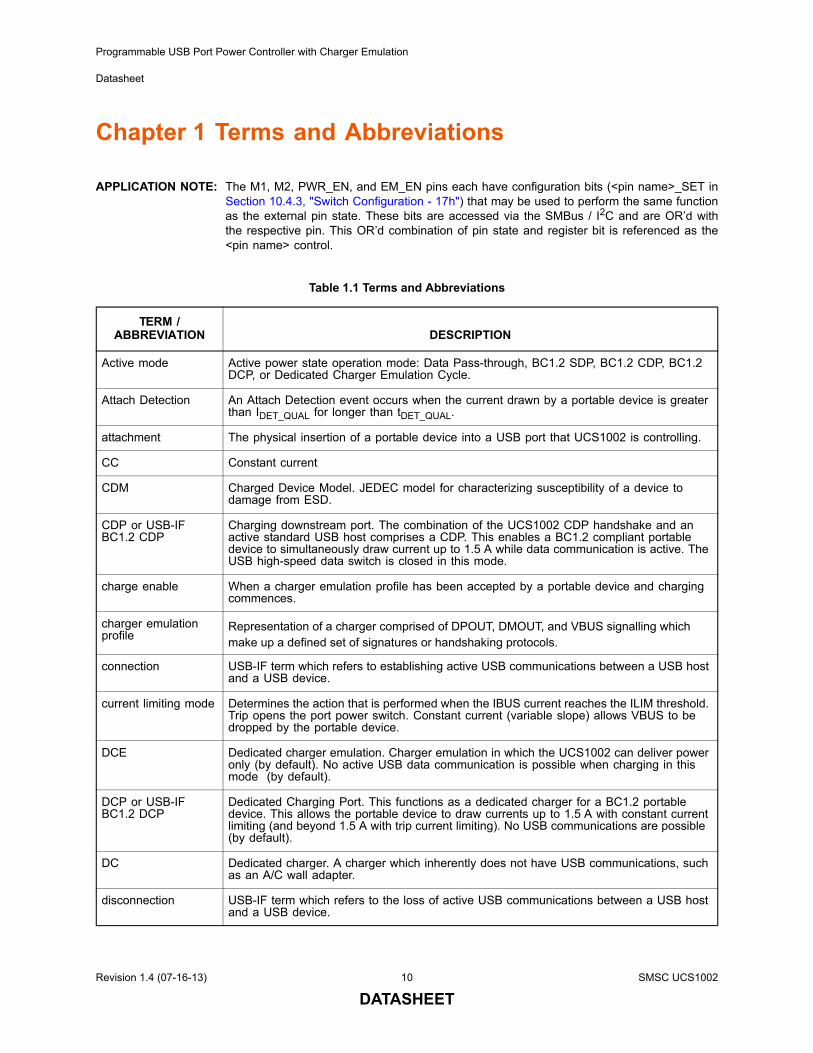
Chapter 1 Terms and Abbreviations
APPLICATION NOTE: The M1, M2, PWR_EN, and EM_EN pins each have configuration bits (<pin name>_SET inSection 10.4.3, "Switch Configuration - 17h") that may be used to perform the same functionas the external pin state. These bits are accessed via the SMBus / I2C and are OR’d withthe respective pin. This OR’d combination of pin state and register bit is referenced as the<pin name> control.
Table 1.1 Terms and Abbreviations
TERM / ABBREVIATION DESCRIPTION
Active mode Active power state operation mode: Data Pass-through, BC1.2 SDP, BC1.2 CDP, BC1.2 DCP, or Dedicated Charger Emulation Cycle.
Attach Detection An Attach Detection event occurs when the current drawn by a portable device is greater than IDET_QUAL for longer than tDET_QUAL.
attachment The physical insertion of a portable device into a USB port that UCS1002 is controlling.
CC Constant current
CDM Charged Device Model. JEDEC model for characterizing susceptibility of a device to damage from ESD.
CDP or USB-IF BC1.2 CDP
Charging downstream port. The combination of the UCS1002 CDP handshake and an active standard USB host comprises a CDP. This enables a BC1.2 compliant portable device to simultaneously draw current up to 1.5 A while data communication is active. The USB high-speed data switch is closed in this mode.
charge enable When a charger emulation profile has been accepted by a portable device and charging commences.
charger emulation profile
Representation of a charger comprised of DPOUT, DMOUT, and VBUS signalling which make up a defined set of signatures or handshaking protocols.
connection USB-IF term which refers to establishing active USB communications between a USB host and a USB device.
current limiting mode Determines the action that is performed when the IBUS current reaches the ILIM threshold. Trip opens the port power switch. Constant current (variable slope) allows VBUS to be dropped by the portable device.
DCE Dedicated charger emulation. Charger emulation in which the UCS1002 can deliver power only (by default). No active USB data communication is possible when charging in this mode (by default).
DCP or USB-IF BC1.2 DCP
Dedicated Charging Port. This functions as a dedicated charger for a BC1.2 portable device. This allows the portable device to draw currents up to 1.5 A with constant current limiting (and beyond 1.5 A with trip current limiting). No USB communications are possible (by default).
DC Dedicated charger. A charger which inherently does not have USB communications, such as an A/C wall adapter.
disconnection USB-IF term which refers to the loss of active USB communications between a USB host and a USB device.
Revision 1.4 (07-16-13) 10 SMSC UCS1002
DATASHEET

Programmable USB Port Power Controller with Charger Emulation
Datasheet
dynamic thermal management
The UCS1002 automatically adjusts port power switch limits and modes to lower internal power dissipation when the thermal regulation temperature value is approached.
enumeration A USB-specific term that indicates that a host is detecting and identifying USB devices.
handshake Application of a charger emulation profile that requires a response. Two-way communication between the UCS1002 and the portable device.
HBM Human Body Model.
HSW High-speed switch.
IBUS_R2MIN Current limiter mode boundary.
ILIM The IBUS current threshold used in current limiting. In trip mode, when ILIM is reached, the port power switch is opened. In constant current mode, when the current exceeds ILIM, operation continues at a reduced voltage and increased current; if VBUS voltage drops below VBUS_MIN, the port power switch is opened.
Legacy USB devices that require non-BC1.2 signatures be applied on the DPOUT and DMOUT pins to enable charging.
OCL Over-current limit.
POR Power-on reset.
portable device USB device attached to the USB port.
power thief A USB device that does not follow the handshaking conventions of a BC1.2 device or Legacy devices and draws current immediately upon receiving power (i.e., a USB book light, portable fan, etc).
Removal Detection A Removal Detection event occurs when the current load on the VBUS pin drops to less than IREM_QUAL for longer than tREM_QUAL.
removal The physical removal of a portable device from a USB port that the UCS1002 is controlling.
response An action, usually in response to a stimulus, in charger emulation performed by the UCS1002 device via the USB data lines.
SDP or USB-IF SDP Standard downstream port. The combination of the UCS1002 high-speed switch being closed with an upstream USB host present comprises a BC1.2 SDP. This enables a BC1.2 compliant portable device to simultaneously draw current up to 0.5 A while data communication is active.
signature Application of a charger emulation profile without waiting for a response. One-way communication from the UCS1002 to the portable device.
Stand-alone mode Indicates that the communications protocol is not active and all communications between the UCS1002 and a controller are done via the external pins only (M1, M2, EM_EN, PWR_EN, S0, and LATCH as inputs and ALERT# and A_DET# as outputs).
stimulus An event in charger emulation detected by the UCS1002 device via the USB data lines.
Table 1.1 Terms and Abbreviations (continued)
TERM / ABBREVIATION DESCRIPTION
SMSC UCS1002 11 Revision 1.4 (07-16-13)
DATASHEET
Programmable USB Port Power Controller with Charger Emulation
Datasheet
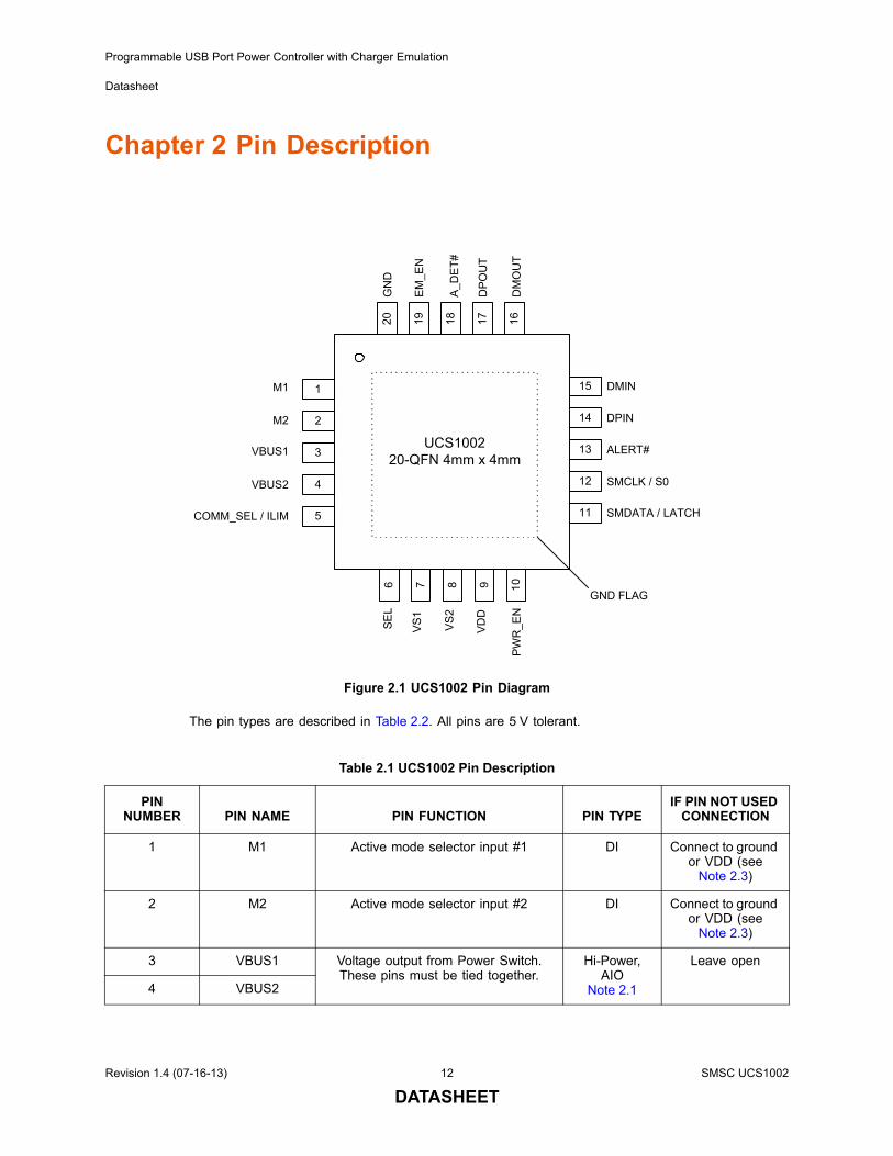
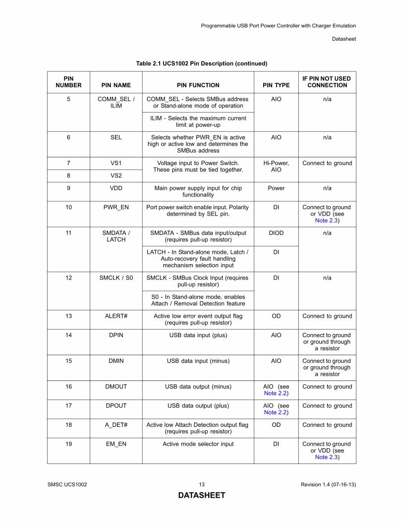
Chapter 2 Pin Description
The pin types are described in Table 2.2. All pins are 5 V tolerant.
Figure 2.1 UCS1002 Pin Diagram
Table 2.1 UCS1002 Pin Description
PIN NUMBER PIN NAME PIN FUNCTION PIN TYPE
IF PIN NOT USED CONNECTION
1 M1 Active mode selector input #1 DI Connect to ground or VDD (see
Note 2.3)
2 M2 Active mode selector input #2 DI Connect to ground or VDD (see
Note 2.3)
3 VBUS1 Voltage output from Power Switch. These pins must be tied together.
Hi-Power, AIO
Note 2.1
Leave open
4 VBUS2
M2
1
2
3
4
6 7 8 9
EM
_EN
M1
510
15
14
13
12
20 19 18 17
PW
R_E
NCOMM_SEL / ILIM
VBUS1
VBUS2
VS
2
VD
D
DPIN
SMCLK / S0
A_D
ET
#
DP
OU
T
SE
L
DM
OU
TSMDATA / LATCH
DMIN
ALERT#
GN
D
VS
1
1116
GND FLAG
UCS1002 20-QFN 4mm x 4mm
Revision 1.4 (07-16-13) 12 SMSC UCS1002
DATASHEET
Programmable USB Port Power Controller with Charger Emulation
Datasheet
5 COMM_SEL / ILIM
COMM_SEL - Selects SMBus address or Stand-alone mode of operation
AIO n/a
ILIM - Selects the maximum current limit at power-up
6 SEL Selects whether PWR_EN is active high or active low and determines the
SMBus address
AIO n/a
7 VS1 Voltage input to Power Switch. These pins must be tied together.
Hi-Power, AIO
Connect to ground
8 VS2
9 VDD Main power supply input for chip functionality
Power n/a
10 PWR_EN Port power switch enable input. Polarity determined by SEL pin.
DI Connect to ground or VDD (see
Note 2.3)
11 SMDATA / LATCH
SMDATA - SMBus data input/output (requires pull-up resistor)
DIOD n/a
LATCH - In Stand-alone mode, Latch / Auto-recovery fault handling mechanism selection input
DI
12 SMCLK / S0 SMCLK - SMBus Clock Input (requires pull-up resistor)
DI n/a
S0 - In Stand-alone mode, enables Attach / Removal Detection feature
13 ALERT# Active low error event output flag (requires pull-up resistor)
OD Connect to ground
14 DPIN USB data input (plus) AIO Connect to ground or ground through
a resistor
15 DMIN USB data input (minus) AIO Connect to ground or ground through
a resistor
16 DMOUT USB data output (minus) AIO (see Note 2.2)
Connect to ground
17 DPOUT USB data output (plus) AIO (see Note 2.2)
Connect to ground
18 A_DET# Active low Attach Detection output flag (requires pull-up resistor)
OD Connect to ground
19 EM_EN Active mode selector input DI Connect to ground or VDD (see
Note 2.3)
Table 2.1 UCS1002 Pin Description (continued)
PIN NUMBER PIN NAME PIN FUNCTION PIN TYPE
IF PIN NOT USED CONNECTION
SMSC UCS1002 13 Revision 1.4 (07-16-13)
DATASHEET
Programmable USB Port Power Controller with Charger Emulation
Datasheet
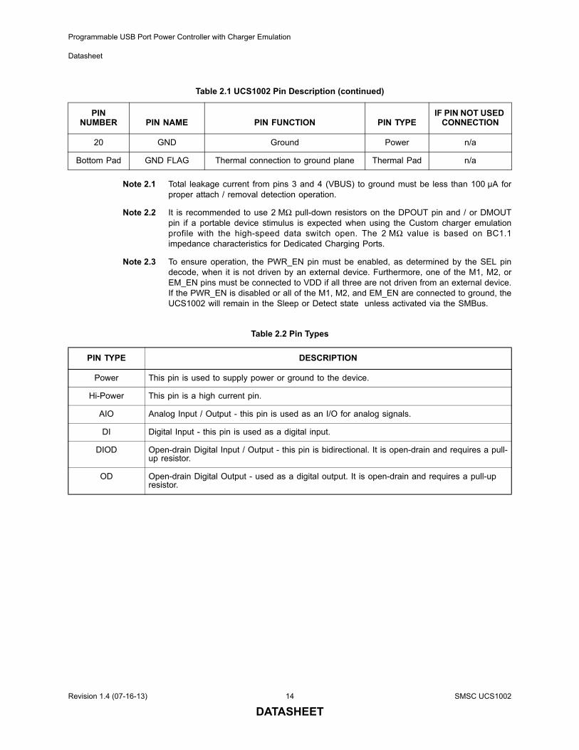
Note 2.1 Total leakage current from pins 3 and 4 (VBUS) to ground must be less than 100 µA forproper attach / removal detection operation.
Note 2.2 It is recommended to use 2 MΩ pull-down resistors on the DPOUT pin and / or DMOUTpin if a portable device stimulus is expected when using the Custom charger emulationprofile with the high-speed data switch open. The 2 MΩ value is based on BC1.1impedance characteristics for Dedicated Charging Ports.
Note 2.3 To ensure operation, the PWR_EN pin must be enabled, as determined by the SEL pindecode, when it is not driven by an external device. Furthermore, one of the M1, M2, orEM_EN pins must be connected to VDD if all three are not driven from an external device.If the PWR_EN is disabled or all of the M1, M2, and EM_EN are connected to ground, theUCS1002 will remain in the Sleep or Detect state unless activated via the SMBus.
20 GND Ground Power n/a
Bottom Pad GND FLAG Thermal connection to ground plane Thermal Pad n/a
Table 2.2 Pin Types
PIN TYPE DESCRIPTION
Power This pin is used to supply power or ground to the device.
Hi-Power This pin is a high current pin.
AIO Analog Input / Output - this pin is used as an I/O for analog signals.
DI Digital Input - this pin is used as a digital input.
DIOD Open-drain Digital Input / Output - this pin is bidirectional. It is open-drain and requires a pull-up resistor.
OD Open-drain Digital Output - used as a digital output. It is open-drain and requires a pull-up resistor.
Table 2.1 UCS1002 Pin Description (continued)
PIN NUMBER PIN NAME PIN FUNCTION PIN TYPE
IF PIN NOT USED CONNECTION
Revision 1.4 (07-16-13) 14 SMSC UCS1002
DATASHEET
Programmable USB Port Power Controller with Charger Emulation
Datasheet
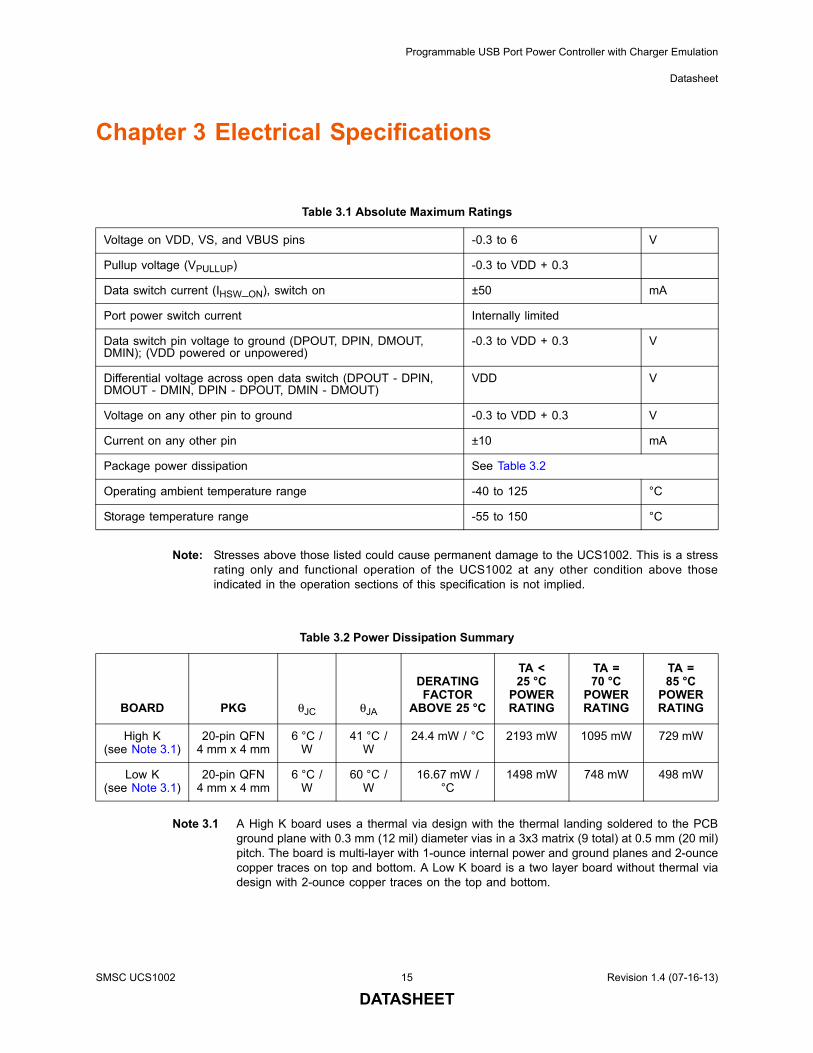
Chapter 3 Electrical Specifications
Note: Stresses above those listed could cause permanent damage to the UCS1002. This is a stressrating only and functional operation of the UCS1002 at any other condition above thoseindicated in the operation sections of this specification is not implied.
Note 3.1 A High K board uses a thermal via design with the thermal landing soldered to the PCBground plane with 0.3 mm (12 mil) diameter vias in a 3x3 matrix (9 total) at 0.5 mm (20 mil)pitch. The board is multi-layer with 1-ounce internal power and ground planes and 2-ouncecopper traces on top and bottom. A Low K board is a two layer board without thermal viadesign with 2-ounce copper traces on the top and bottom.
Table 3.1 Absolute Maximum Ratings
Voltage on VDD, VS, and VBUS pins -0.3 to 6 V
Pullup voltage (VPULLUP) -0.3 to VDD + 0.3
Data switch current (IHSW_ON), switch on ±50 mA
Port power switch current Internally limited
Data switch pin voltage to ground (DPOUT, DPIN, DMOUT, DMIN); (VDD powered or unpowered)
-0.3 to VDD + 0.3 V
Differential voltage across open data switch (DPOUT - DPIN, DMOUT - DMIN, DPIN - DPOUT, DMIN - DMOUT)
VDD V
Voltage on any other pin to ground -0.3 to VDD + 0.3 V
Current on any other pin ±10 mA
Package power dissipation See Table 3.2
Operating ambient temperature range -40 to 125 °C
Storage temperature range -55 to 150 °C
Table 3.2 Power Dissipation Summary
BOARD PKG θJC θJA
DERATING FACTOR
ABOVE 25 °C
TA < 25 °C
POWER RATING
TA = 70 °C
POWER RATING
TA = 85 °C
POWER RATING
High K(see Note 3.1)
20-pin QFN 4 mm x 4 mm
6 °C / W
41 °C / W
24.4 mW / °C 2193 mW 1095 mW 729 mW
Low K(see Note 3.1)
20-pin QFN 4 mm x 4 mm
6 °C / W
60 °C / W
16.67 mW / °C
1498 mW 748 mW 498 mW
SMSC UCS1002 15 Revision 1.4 (07-16-13)
DATASHEET
Programmable USB Port Power Controller with Charger Emulation
Datasheet
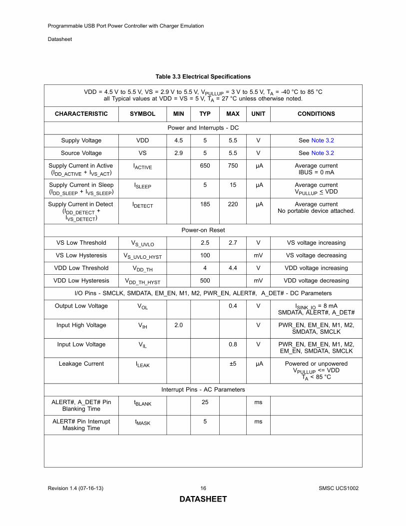
Table 3.3 Electrical Specifications
VDD = 4.5 V to 5.5 V, VS = 2.9 V to 5.5 V, VPULLUP = 3 V to 5.5 V, TA = -40 °C to 85 °Call Typical values at VDD = VS = 5 V, TA = 27 °C unless otherwise noted.
CHARACTERISTIC SYMBOL MIN TYP MAX UNIT CONDITIONS
Power and Interrupts - DC
Supply Voltage VDD 4.5 5 5.5 V See Note 3.2
Source Voltage VS 2.9 5 5.5 V See Note 3.2
Supply Current in Active (IDD_ACTIVE + IVS_ACT)
IACTIVE 650 750 µA Average currentIBUS = 0 mA
Supply Current in Sleep(IDD_SLEEP + IVS_SLEEP)
ISLEEP 5 15 µA Average currentVPULLUP < VDD
Supply Current in Detect (IDD_DETECT + IVS_DETECT)
IDETECT 185 220 µA Average currentNo portable device attached.
Power-on Reset
VS Low Threshold VS_UVLO 2.5 2.7 V VS voltage increasing
VS Low Hysteresis VS_UVLO_HYST 100 mV VS voltage decreasing
VDD Low Threshold VDD_TH 4 4.4 V VDD voltage increasing
VDD Low Hysteresis VDD_TH_HYST 500 mV VDD voltage decreasing
I/O Pins - SMCLK, SMDATA, EM_EN, M1, M2, PWR_EN, ALERT#, A_DET# - DC Parameters
Output Low Voltage VOL 0.4 V ISINK_IO = 8 mASMDATA, ALERT#, A_DET#
Input High Voltage VIH 2.0 V PWR_EN, EM_EN, M1, M2, SMDATA, SMCLK
Input Low Voltage VIL 0.8 V PWR_EN, EM_EN, M1, M2, EM_EN, SMDATA, SMCLK
Leakage Current ILEAK ±5 µA Powered or unpoweredVPULLUP <= VDD
TA < 85 °C
Interrupt Pins - AC Parameters
ALERT#, A_DET# Pin Blanking Time
tBLANK 25 ms
ALERT# Pin Interrupt Masking Time
tMASK 5 ms
Revision 1.4 (07-16-13) 16 SMSC UCS1002
DATASHEET
Programmable USB Port Power Controller with Charger Emulation
Datasheet
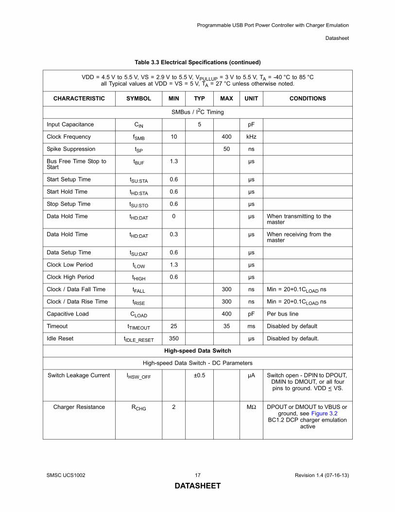
SMBus / I2C Timing
Input Capacitance CIN 5 pF
Clock Frequency fSMB 10 400 kHz
Spike Suppression tSP 50 ns
Bus Free Time Stop to Start
tBUF 1.3 µs
Start Setup Time tSU:STA 0.6 µs
Start Hold Time tHD:STA 0.6 µs
Stop Setup Time tSU:STO 0.6 µs
Data Hold Time tHD:DAT 0 µs When transmitting to the master
Data Hold Time tHD:DAT 0.3 µs When receiving from the master
Data Setup Time tSU:DAT 0.6 µs
Clock Low Period tLOW 1.3 µs
Clock High Period tHIGH 0.6 µs
Clock / Data Fall Time tFALL 300 ns Min = 20+0.1CLOAD ns
Clock / Data Rise Time tRISE 300 ns Min = 20+0.1CLOAD ns
Capacitive Load CLOAD 400 pF Per bus line
Timeout tTIMEOUT 25 35 ms Disabled by default
Idle Reset tIDLE_RESET 350 µs Disabled by default.
High-speed Data Switch
High-speed Data Switch - DC Parameters
Switch Leakage Current IHSW_OFF ±0.5 µA Switch open - DPIN to DPOUT, DMIN to DMOUT, or all four pins to ground. VDD < VS.
Charger Resistance RCHG 2 MΩ DPOUT or DMOUT to VBUS or ground, see Figure 3.2
BC1.2 DCP charger emulation active
Table 3.3 Electrical Specifications (continued)
VDD = 4.5 V to 5.5 V, VS = 2.9 V to 5.5 V, VPULLUP = 3 V to 5.5 V, TA = -40 °C to 85 °Call Typical values at VDD = VS = 5 V, TA = 27 °C unless otherwise noted.
CHARACTERISTIC SYMBOL MIN TYP MAX UNIT CONDITIONS
SMSC UCS1002 17 Revision 1.4 (07-16-13)
DATASHEET
Programmable USB Port Power Controller with Charger Emulation
Datasheet
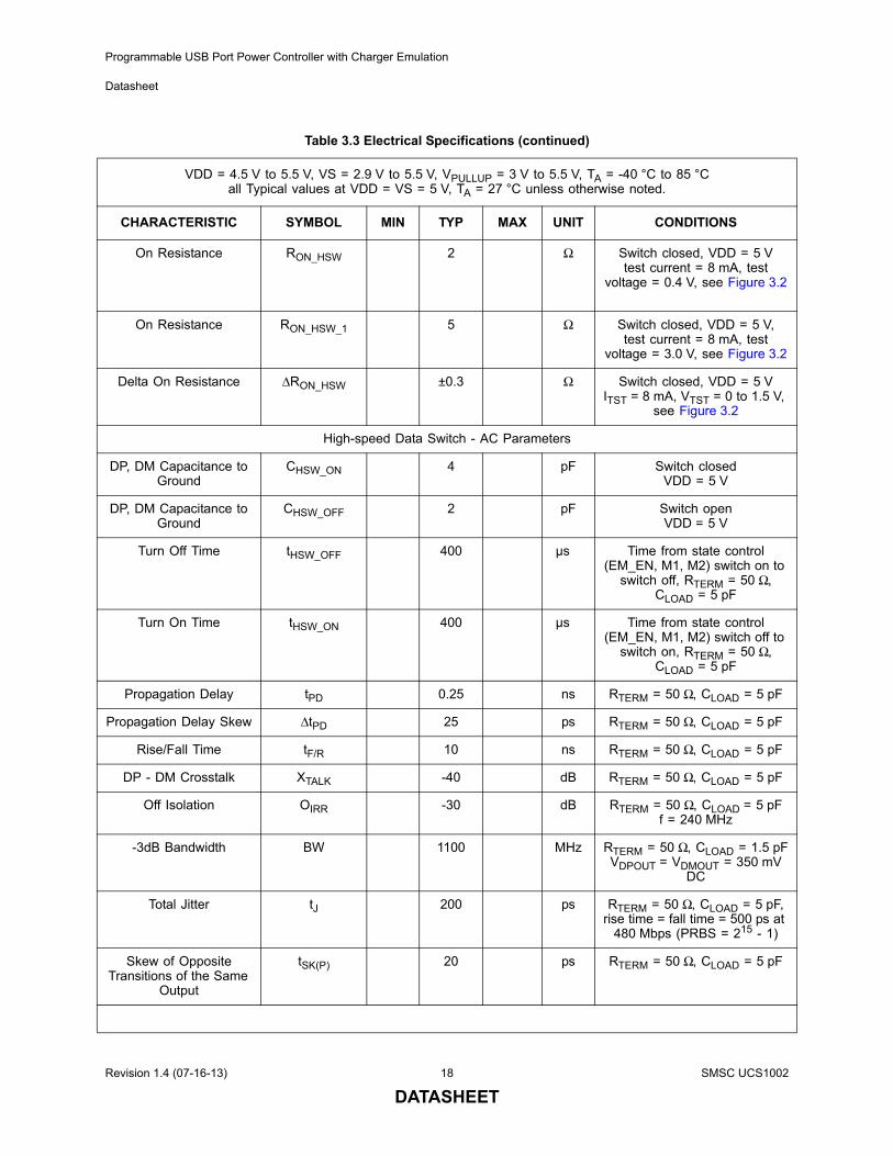
On Resistance RON_HSW 2 Ω Switch closed, VDD = 5 Vtest current = 8 mA, test
voltage = 0.4 V, see Figure 3.2
On Resistance RON_HSW_1 5 Ω Switch closed, VDD = 5 V,test current = 8 mA, test
voltage = 3.0 V, see Figure 3.2
Delta On Resistance ΔRON_HSW ±0.3 Ω Switch closed, VDD = 5 VITST = 8 mA, VTST = 0 to 1.5 V,
see Figure 3.2
High-speed Data Switch - AC Parameters
DP, DM Capacitance to Ground
CHSW_ON 4 pF Switch closedVDD = 5 V
DP, DM Capacitance to Ground
CHSW_OFF 2 pF Switch openVDD = 5 V
Turn Off Time tHSW_OFF 400 µs Time from state control (EM_EN, M1, M2) switch on to
switch off, RTERM = 50 Ω, CLOAD = 5 pF
Turn On Time tHSW_ON 400 µs Time from state control (EM_EN, M1, M2) switch off to
switch on, RTERM = 50 Ω, CLOAD = 5 pF
Propagation Delay tPD 0.25 ns RTERM = 50 Ω, CLOAD = 5 pF
Propagation Delay Skew ΔtPD 25 ps RTERM = 50 Ω, CLOAD = 5 pF
Rise/Fall Time tF/R 10 ns RTERM = 50 Ω, CLOAD = 5 pF
DP - DM Crosstalk XTALK -40 dB RTERM = 50 Ω, CLOAD = 5 pF
Off Isolation OIRR -30 dB RTERM = 50 Ω, CLOAD = 5 pFf = 240 MHz
-3dB Bandwidth BW 1100 MHz RTERM = 50 Ω, CLOAD = 1.5 pFVDPOUT = VDMOUT = 350 mV
DC
Total Jitter tJ 200 ps RTERM = 50 Ω, CLOAD = 5 pF, rise time = fall time = 500 ps at
480 Mbps (PRBS = 215 - 1)
Skew of Opposite Transitions of the Same
Output
tSK(P) 20 ps RTERM = 50 Ω, CLOAD = 5 pF
Table 3.3 Electrical Specifications (continued)
VDD = 4.5 V to 5.5 V, VS = 2.9 V to 5.5 V, VPULLUP = 3 V to 5.5 V, TA = -40 °C to 85 °Call Typical values at VDD = VS = 5 V, TA = 27 °C unless otherwise noted.
CHARACTERISTIC SYMBOL MIN TYP MAX UNIT CONDITIONS
Revision 1.4 (07-16-13) 18 SMSC UCS1002
DATASHEET
Programmable USB Port Power Controller with Charger Emulation
Datasheet
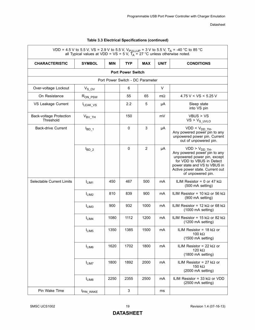
Port Power Switch
Port Power Switch - DC Parameter
Over-voltage Lockout VS_OV 6 V
On Resistance RON_PSW 55 65 mΩ 4.75 V < VS < 5.25 V
VS Leakage Current ILEAK_VS 2.2 5 µA Sleep stateinto VS pin
Back-voltage Protection Threshold
VBV_TH 150 mV VBUS > VSVS > VS_UVLO
Back-drive Current IBD_1 0 3 µA VDD < VDD_TH,Any powered power pin to any unpowered power pin. Current
out of unpowered pin.
IBD_2 0 2 µA VDD > VDD_TH,Any powered power pin to any unpowered power pin, except for VDD to VBUS in Detect
power state and VS to VBUS in Active power state. Current out
of unpowered pin.
Selectable Current Limits ILIM1 450 467 500 mA ILIM Resistor = 0 or 47 kΩ(500 mA setting)
ILIM2 810 839 900 mA ILIM Resistor = 10 kΩ or 56 kΩ(900 mA setting)
ILIM3 900 932 1000 mA ILIM Resistor = 12 kΩ or 68 kΩ(1000 mA setting)
ILIM4 1080 1112 1200 mA ILIM Resistor = 15 kΩ or 82 kΩ(1200 mA setting)
ILIM5 1350 1385 1500 mA ILIM Resistor = 18 kΩ or 100 kΩ
(1500 mA setting)
ILIM6 1620 1702 1800 mA ILIM Resistor = 22 kΩ or 120 kΩ
(1800 mA setting)
ILIM7 1800 1892 2000 mA ILIM Resistor = 27 kΩ or 150 kΩ
(2000 mA setting)
ILIM8 2250 2355 2500 mA ILIM Resistor = 33 kΩ or VDD(2500 mA setting)
Pin Wake Time tPIN_WAKE 3 ms
Table 3.3 Electrical Specifications (continued)
VDD = 4.5 V to 5.5 V, VS = 2.9 V to 5.5 V, VPULLUP = 3 V to 5.5 V, TA = -40 °C to 85 °Call Typical values at VDD = VS = 5 V, TA = 27 °C unless otherwise noted.
CHARACTERISTIC SYMBOL MIN TYP MAX UNIT CONDITIONS
SMSC UCS1002 19 Revision 1.4 (07-16-13)
DATASHEET
Programmable USB Port Power Controller with Charger Emulation
Datasheet
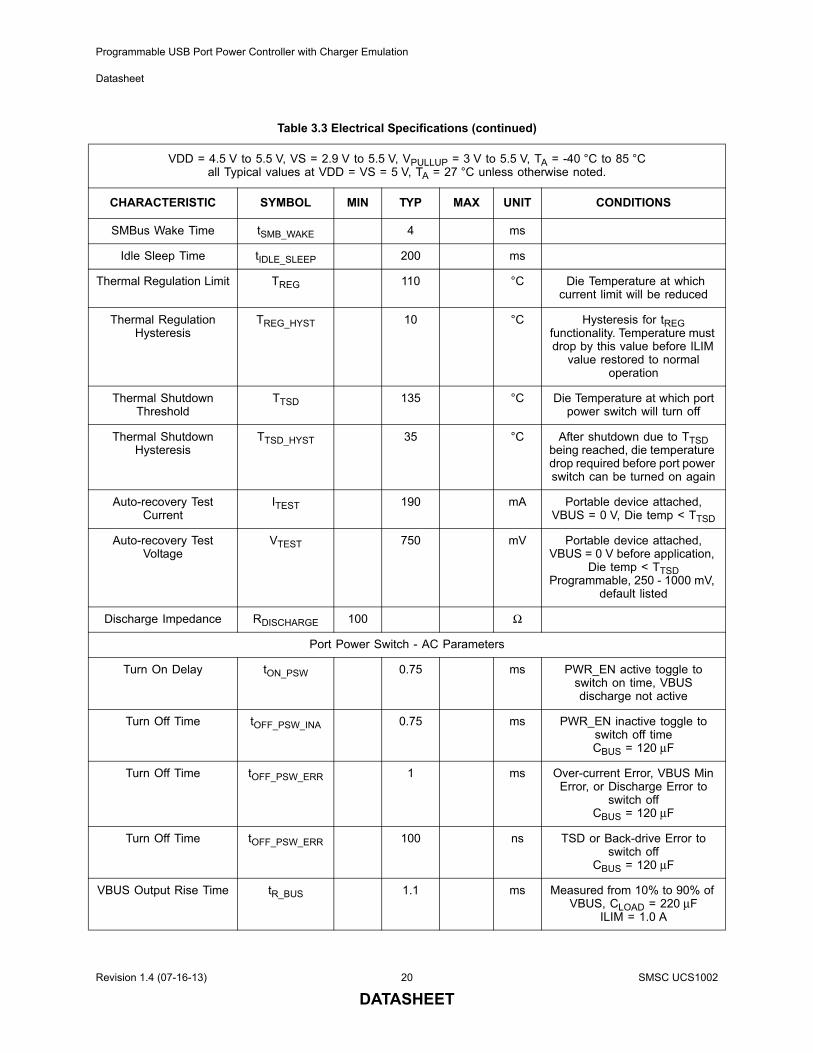
SMBus Wake Time tSMB_WAKE 4 ms
Idle Sleep Time tIDLE_SLEEP 200 ms
Thermal Regulation Limit TREG 110 °C Die Temperature at which current limit will be reduced
Thermal Regulation Hysteresis
TREG_HYST 10 °C Hysteresis for tREG functionality. Temperature must drop by this value before ILIM
value restored to normal operation
Thermal Shutdown Threshold
TTSD 135 °C Die Temperature at which port power switch will turn off
Thermal Shutdown Hysteresis
TTSD_HYST 35 °C After shutdown due to TTSD being reached, die temperature drop required before port power switch can be turned on again
Auto-recovery Test Current
ITEST 190 mA Portable device attached, VBUS = 0 V, Die temp < TTSD
Auto-recovery Test Voltage
VTEST 750 mV Portable device attached, VBUS = 0 V before application,
Die temp < TTSDProgrammable, 250 - 1000 mV,
default listed
Discharge Impedance RDISCHARGE 100 Ω
Port Power Switch - AC Parameters
Turn On Delay tON_PSW 0.75 ms PWR_EN active toggle to switch on time, VBUS discharge not active
Turn Off Time tOFF_PSW_INA 0.75 ms PWR_EN inactive toggle to switch off timeCBUS = 120 μF
Turn Off Time tOFF_PSW_ERR 1 ms Over-current Error, VBUS Min Error, or Discharge Error to
switch off CBUS = 120 μF
Turn Off Time tOFF_PSW_ERR 100 ns TSD or Back-drive Error to switch off
CBUS = 120 μF
VBUS Output Rise Time tR_BUS 1.1 ms Measured from 10% to 90% of VBUS, CLOAD = 220 μF
ILIM = 1.0 A
Table 3.3 Electrical Specifications (continued)
VDD = 4.5 V to 5.5 V, VS = 2.9 V to 5.5 V, VPULLUP = 3 V to 5.5 V, TA = -40 °C to 85 °Call Typical values at VDD = VS = 5 V, TA = 27 °C unless otherwise noted.
CHARACTERISTIC SYMBOL MIN TYP MAX UNIT CONDITIONS
Revision 1.4 (07-16-13) 20 SMSC UCS1002
DATASHEET
Programmable USB Port Power Controller with Charger Emulation
Datasheet
Soft Turn on Rate ΔIBUS / Δt 100 mA / µs
Temperature Update Time
tDC_TEMP 200 ms Programmable 200 - 1600 ms, default listed
Short Circuit Response Time
tSHORT_LIM 1.5 µs Time from detection of short to current limit applied.
No CBUS applied
Short Circuit Detection Time
tSHORT 6 ms Time from detection of short to port power switch disconnect and ALERT# pin assertion.
Latched Mode Cycle Time
tUL 7 ms From PWR_EN edge transition from inactive to active to begin
error recovery
Auto-recovery Mode Cycle Time
tCYCLE 25 ms Time delay before error condition check
Programmable 15-50 ms, default listed
Auto-recovery Delay tRST 20 ms Portable device attached, VBUS must be > VTEST after
this timeProgrammable 10-25 ms,
default listed
Discharge Time tDISCHARGE 200 ms Amount of time discharge resistor applied
Programmable 100-400 ms, default listed
Port Power Switch Operation With Trip Mode Current Limiting
Region 2 Current Keep-out
IBUS_R2MIN 0.1 A
Minimum VBUS Allowed at Output
VBUS_MIN 2.0 V
Port Power Switch Operation With Constant Current Limiting (Variable Slope)
Region 2 Current Keep-out
IBUS_R2MIN 1.5 A
Minimum VBUS Allowed at Output
VBUS_MIN 2.0 V
Port Power Switch Operation With Custom Current Limiting
Region 2 Current Keep-out
IBUS_R2MIN 0.1 A Programmable from 100 mA to 1.8 A. Default value listed.
Table 3.3 Electrical Specifications (continued)
VDD = 4.5 V to 5.5 V, VS = 2.9 V to 5.5 V, VPULLUP = 3 V to 5.5 V, TA = -40 °C to 85 °Call Typical values at VDD = VS = 5 V, TA = 27 °C unless otherwise noted.
CHARACTERISTIC SYMBOL MIN TYP MAX UNIT CONDITIONS
SMSC UCS1002 21 Revision 1.4 (07-16-13)
DATASHEET
Programmable USB Port Power Controller with Charger Emulation
Datasheet
Minimum VBUS Allowed at Output
VBUS_MIN 2.0 V Programmable from 1.5 V to 2.25 V. Default value listed.
Current Measurement - DC
Current Measurement Range
IBUS_M 6.4 2500 mA Range (see Note 3.3)
Reported Current Measurement Resolution
ΔIBUS_M 9.76 mA 1 LSB
Current Measurement Accuracy
±2 % ILIM not exceeded
Current Measurement - AC
Sampling Rate 500 µs
Charge Rationing - DC
Accumulated Current Measurement Accuracy
±4.5 %
Charge Rationing - AC
Current Measurement Update Time
tPCYCLE 1 s
Attach / Removal Detection
VBUS Bypass - DC
On Resistance RON_BYP 50 Ω
Leakage Current ILEAK_BYP 3 µA Switch off
Current Limit IDET_CHG / IBUS_BYP
2 mA VDD = 5 V and VBUS> 4.75 V
Attach / Removal Detection - DC
Attach Detection Threshold
IDET_QUAL 800 µA Programmable 200-1000 µA, default listed
Primary Removal Detection Threshold
IREM_QUAL_ACT 700 µAProgrammable 100-900 µA,
default listedActive power state
IREM_QUAL_DET 800 µA Programmable 200-1000 µA, default listed
Detect power state(see Section 8.4)
Table 3.3 Electrical Specifications (continued)
VDD = 4.5 V to 5.5 V, VS = 2.9 V to 5.5 V, VPULLUP = 3 V to 5.5 V, TA = -40 °C to 85 °Call Typical values at VDD = VS = 5 V, TA = 27 °C unless otherwise noted.
CHARACTERISTIC SYMBOL MIN TYP MAX UNIT CONDITIONS
Revision 1.4 (07-16-13) 22 SMSC UCS1002
DATASHEET
Programmable USB Port Power Controller with Charger Emulation
Datasheet
Attach / Removal Detection - AC
Attach Detection Time tDET_QUAL 100 ms Time from Attach to A_DET# assert .
Removal Detection Time tREM_QUAL 1000 ms
Allowed Charge Time tDET_CHARGE 800 ms CBUS = 500 µF maxProgrammable 200-2000 ms,
default listed
Charger Emulation Profile
General Emulation - DC
Charging Current Threshold
IBUS_CHG 9.76 mA default
Charging Current Threshold Range
IBUS_CHG_RNG 9.76 155 mA Programmable, all typical
DP-DM Shunt Resistor Value
RDCP_RES 200 Ω Connected between DPOUT and DMOUT
0 V < DPOUT = DMOUT < 3 V
Response Magnitude (voltage divider option min resistance range)
SX_RXMAG_DVDR
93 200 kΩ Programmable, all mins
Resistor Ratio Range (voltage divider option)
SX_RATIO 0.25 0.66 V / V Programmable, all typical
Resistor Ratio Accuracy (voltage divider option)
SX_RATIO_ ACC
±0.5 % Average over range
Response Magnitude (resistor option range)
SX_RXMAG_RES
1.8 150 kΩ Programmable, all typical
Internal Resistor Tolerance (resistor
option)
SX_RXMAG_RES_ACC
±10 % Average over range
Response Magnitude (voltage option range)
SX_RXMAG_VOLT
0.4 2.2 V Programmable, all typical
Voltage Option Accuracy SX_RXMAG_VOLT_ACC
±1 % No loadAverage over range
Voltage Option Accuracy SX_RXMAG_VOLT_ACC_
150
-6 % 150 µA loadAverage over range
Voltage Option Accuracy SX_RXMAG_VOLT_ACC_
250
-10 % 250 µA loadAverage over range
Table 3.3 Electrical Specifications (continued)
VDD = 4.5 V to 5.5 V, VS = 2.9 V to 5.5 V, VPULLUP = 3 V to 5.5 V, TA = -40 °C to 85 °Call Typical values at VDD = VS = 5 V, TA = 27 °C unless otherwise noted.
CHARACTERISTIC SYMBOL MIN TYP MAX UNIT CONDITIONS
SMSC UCS1002 23 Revision 1.4 (07-16-13)
DATASHEET
Programmable USB Port Power Controller with Charger Emulation
Datasheet
Note 3.2 For split supply systems using the Attach Detection feature, VS must not exceed VDD +150 mV.
Note 3.3 The current measurement full scale range maximum value is 2.5 A. However, theUCS1002 cannot report values above ILIM (if IBUS_R2MIN < ILIM) or above IBUS_R2MIN (ifIBUS_R2MIN > ILIM and ILIM < 1.5 A).
Voltage Option Output SX_RXMAG_VOLT_BC
0.5 V DMOUT = 0.6 V250 µA load
Response Magnitude (zero volt option range)
SX_PUPD 10 150 µA SX_RXMAG_VOLT = 0Programmable, all typical
Pull-down Current Accuracy
SX_PUPD _ACC_3p6
±5 % DPOUT or DMOUT = 3.6 V Compliance voltage
Pull-down Current SX_PUPD _ACC_BC
50 µA Setting = 100 µADPOUT or DMOUT = 0.15 V
Compliance voltage
Stimulus Voltage Threshold Range
SX_TH 0.3 2.2 V Programmable, all typical
Stimulus Voltage Accuracy
SX_TH_ ACC ±2 % Average over range
Stimulus Voltage Accuracy
SX_TH_ACC_BC
0.25 V At SX_TH = 0.3 V
Stimulus Voltage Hysteresis
SX_TH_HYST 40 mV Voltage falling
General Emulation - AC
Emulation Reset Time tEM_RESET 50 ms default
Emulation Reset Time Range
tEM_RESET_ RNG
50 175 ms Programmable, all typical
Emulation Timeout Range
tEM_ TIMEOUT 0.8 12.8 s Programmable, 0.8 s to 12.8 s, all typical
Stimulus Delay, SX_TD Range
tSTIM_DEL 0 100 ms Programmable, all typical
Emulation Delay tRES_EM 0.5 s Time from set impedance to impedance appears on DP /
DM
Table 3.3 Electrical Specifications (continued)
VDD = 4.5 V to 5.5 V, VS = 2.9 V to 5.5 V, VPULLUP = 3 V to 5.5 V, TA = -40 °C to 85 °Call Typical values at VDD = VS = 5 V, TA = 27 °C unless otherwise noted.
CHARACTERISTIC SYMBOL MIN TYP MAX UNIT CONDITIONS
Revision 1.4 (07-16-13) 24 SMSC UCS1002
DATASHEET
Programmable USB Port Power Controller with Charger Emulation
Datasheet
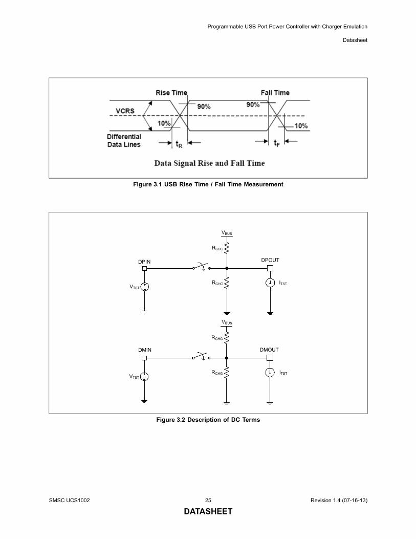
Figure 3.1 USB Rise Time / Fall Time Measurement
Figure 3.2 Description of DC Terms
DPIN DPOUT
RCHG
VBUS
VTST
RCHG
ITST
DMIN
RCHG
VBUS
VTST
RCHG
ITST
DMOUT
SMSC UCS1002 25 Revision 1.4 (07-16-13)
DATASHEET
Programmable USB Port Power Controller with Charger Emulation
Datasheet
Revision 1.4 (07-16-13) 26 SMSC UCS1002
DATASHEET
3.1 ESD & Transient Performance
APPLICATION NOTE: Depending on the level of ESD protection required by the application, external protectiondevices may be required. The datasheet ESD levels were reached using external devicesand standard USB-A connectors; refer to the EVB schematic and reference design fordetails.
Note 3.4 Operational Classification B indicates that during and immediately after an ESD event,anomalous behavior may occur; however, it is non-damaging and the device is self-recovering. All IEC testing is performed using an SMSC evaluation board.
Note 3.5 Operational Classification A indicates that during and immediately after an ESD event noanomalous behavior will occur. All IEC testing is performed using an SMSC evaluationboard.
3.1.1 Human Body Model (HBM) Performance
HBM testing verifies the ability to withstand ESD strikes like those that occur during handling andmanufacturing and is done without power applied to the IC. To pass the test, the device must have nochange in operation or performance due to the event.
3.1.2 Charged Device Model (CDM) Performance
CDM testing verifies the ability to withstand ESD strikes like those that occur during handling andassembly with pick and place style machinery and is done without power applied to the IC. To passthe test, the device must have no change in operation or performance due to the event.
3.1.3 IEC61000-4-2 Performance
The IEC61000-4-2 ESD specification is an international standard that addresses system-level immunityto ESD strikes while the end equipment is operational. These tests are performed while the device ispowered.
Table 3.4 ESD Ratings
ESD SPEC RATING OR VALUE
EN / IEC61000-4-2 (DPOUT, DMOUT pins) air gap, Operational Classification B (see Note 3.4)
Level 4 (15 kV)
EN / IEC61000-4-2 (DPOUT, DMOUT pins) direct contact, Operational Classification B (see Note 3.4)
Level 4 (8 kV)
EN / IEC61000-4-2 (VBUS, GND pins) air gap, Operational Classification A (see Note 3.5)
Level 4 (15 kV)
EN / IEC61000-4-2 (VBUS, GND pins) direct contact, Operational Classification A (see Note 3.5)
Level 4 (8 kV)
Human Body Model (JEDEC JESD22-A114) - All pins 8 kV
Charged Device Model (JEDEC JESD22-C101) - All pins 500 V
Programmable USB Port Power Controller with Charger Emulation
Datasheet
Chapter 4 Communications
4.1 Operating Mode
The UCS1002 can operate in SMBus mode (see Section 4.2, "SMBus Operating Mode") or Stand-alone mode (see Section 4.3, "Stand-alone Operating Mode"). The resistor on the COMM_SEL / ILIMpin determines operating mode and the hardware-set ILIM setting, as shown in Table 4.1. Unlessconnected to GND or VDD, the resistors in Table 4.1 are pull-down resistors.
APPLICATION NOTE: If it is necessary to connect the COMM_SEL / ILIM pin to VDD via a pull-up resistor, it isrecommended that this resistor value not exceed 100 kΩ.
Table 4.1 UCS1002 Communication Mode and ILIM Selection
SELECTION RESISTOR ±5% ILIM SETTING COMMUNICATIONS MODE
GND 500 mA SMBus - see Section 4.2.1.2
10 kΩ pull-down 900 mA SMBus - see Section 4.2.1.2
12 kΩ pull-down 1000 mA SMBus - see Section 4.2.1.2
15 kΩ pull-down 1200 mA SMBus - see Section 4.2.1.2
18 kΩ pull-down 1500 mA SMBus - see Section 4.2.1.2
22 kΩ pull-down 1800 mA SMBus - see Section 4.2.1.2
27 kΩ pull-down 2000 mA SMBus - see Section 4.2.1.2
33 kΩ pull-down 2500 mA SMBus - see Section 4.2.1.2
47 kΩ pull-down 500 mA Stand-alone mode
56 kΩ pull-down 900 mA Stand-alone mode
68 kΩ pull-down 1000 mA Stand-alone mode
82 kΩ pull-down 1200 mA Stand-alone mode
100 kΩ pull-down 1500 mA Stand-alone mode
120 kΩ pull-down 1800 mA Stand-alone mode
150 kΩ pull-down 2000 mA Stand-alone mode
VDD(If a pull-up resistor is used, its value must not exceed 100 kΩ.)
2500 mA Stand-alone mode
SMSC UCS1002 27 Revision 1.4 (07-16-13)
DATASHEET
Programmable USB Port Power Controller with Charger Emulation
Datasheet
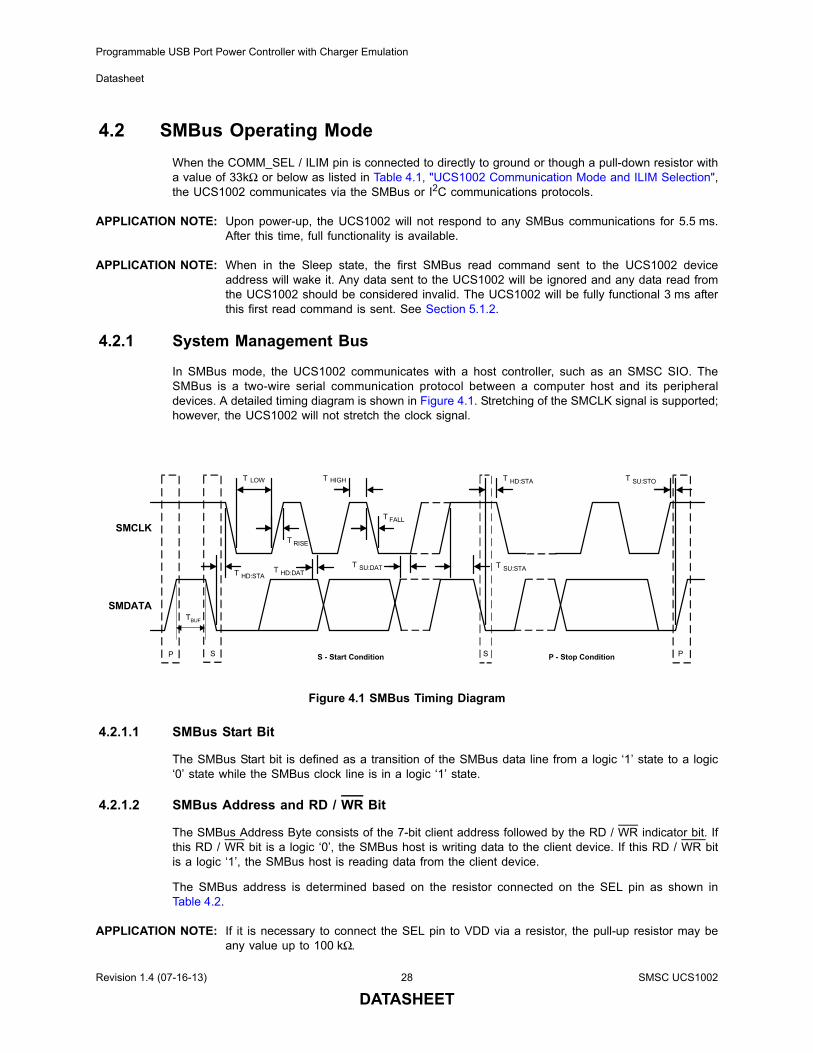
4.2 SMBus Operating Mode
When the COMM_SEL / ILIM pin is connected to directly to ground or though a pull-down resistor witha value of 33kΩ or below as listed in Table 4.1, "UCS1002 Communication Mode and ILIM Selection",the UCS1002 communicates via the SMBus or I2C communications protocols.
APPLICATION NOTE: Upon power-up, the UCS1002 will not respond to any SMBus communications for 5.5 ms.After this time, full functionality is available.
APPLICATION NOTE: When in the Sleep state, the first SMBus read command sent to the UCS1002 deviceaddress will wake it. Any data sent to the UCS1002 will be ignored and any data read fromthe UCS1002 should be considered invalid. The UCS1002 will be fully functional 3 ms afterthis first read command is sent. See Section 5.1.2.
4.2.1 System Management Bus
In SMBus mode, the UCS1002 communicates with a host controller, such as an SMSC SIO. TheSMBus is a two-wire serial communication protocol between a computer host and its peripheraldevices. A detailed timing diagram is shown in Figure 4.1. Stretching of the SMCLK signal is supported;however, the UCS1002 will not stretch the clock signal.
4.2.1.1 SMBus Start Bit
The SMBus Start bit is defined as a transition of the SMBus data line from a logic ‘1’ state to a logic‘0’ state while the SMBus clock line is in a logic ‘1’ state.
4.2.1.2 SMBus Address and RD / WR Bit
The SMBus Address Byte consists of the 7-bit client address followed by the RD / WR indicator bit. Ifthis RD / WR bit is a logic ‘0’, the SMBus host is writing data to the client device. If this RD / WR bitis a logic ‘1’, the SMBus host is reading data from the client device.
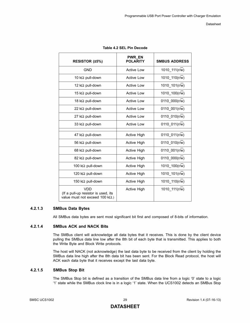
The SMBus address is determined based on the resistor connected on the SEL pin as shown inTable 4.2.
APPLICATION NOTE: If it is necessary to connect the SEL pin to VDD via a resistor, the pull-up resistor may beany value up to 100 kΩ.
Figure 4.1 SMBus Timing Diagram
SMDATA
SMCLK
TBUF
P S S - Start Condition P - Stop Condition PS
T HIGHT LOW T HD:STA T SU:STO
T HD:STAT HD:DAT
T SU:DAT T SU:STA
T FALL
T RISE
Revision 1.4 (07-16-13) 28 SMSC UCS1002
DATASHEET
Programmable USB Port Power Controller with Charger Emulation
Datasheet
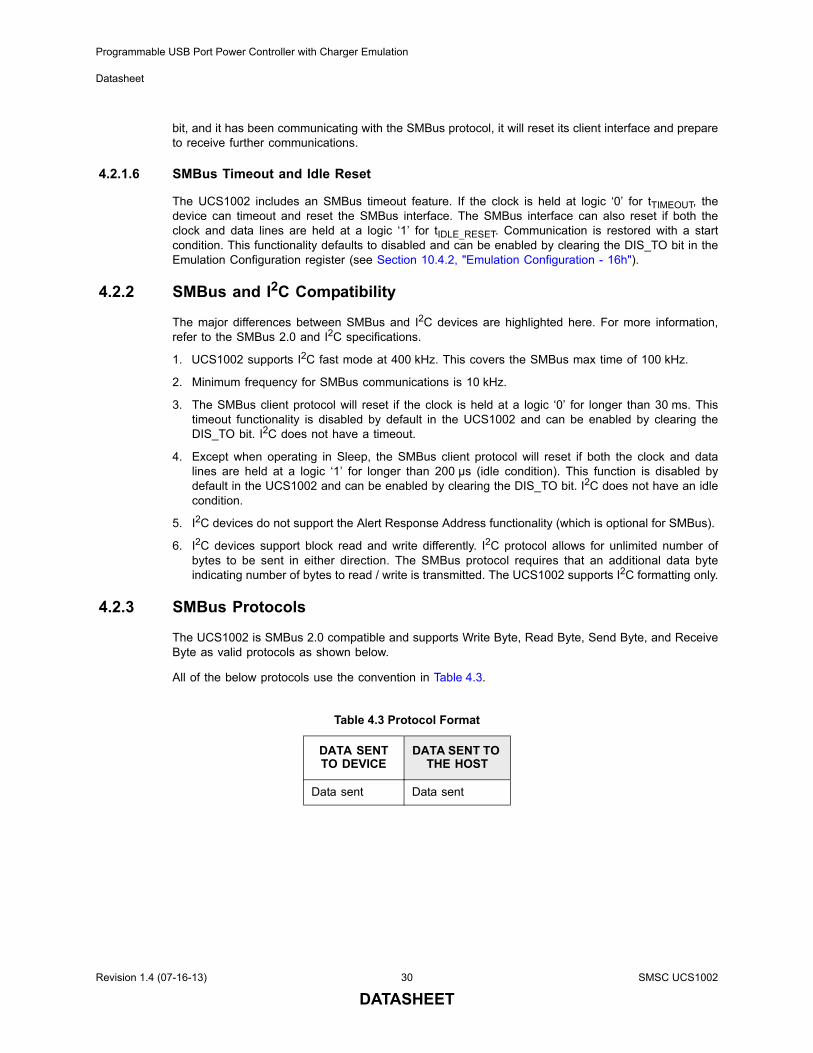
4.2.1.3 SMBus Data Bytes
All SMBus data bytes are sent most significant bit first and composed of 8-bits of information.
4.2.1.4 SMBus ACK and NACK Bits
The SMBus client will acknowledge all data bytes that it receives. This is done by the client devicepulling the SMBus data line low after the 8th bit of each byte that is transmitted. This applies to boththe Write Byte and Block Write protocols.
The host will NACK (not acknowledge) the last data byte to be received from the client by holding theSMBus data line high after the 8th data bit has been sent. For the Block Read protocol, the host willACK each data byte that it receives except the last data byte.
4.2.1.5 SMBus Stop Bit
The SMBus Stop bit is defined as a transition of the SMBus data line from a logic ‘0’ state to a logic‘1’ state while the SMBus clock line is in a logic ‘1’ state. When the UCS1002 detects an SMBus Stop
Table 4.2 SEL Pin Decode
RESISTOR (±5%)PWR_EN
POLARITY SMBUS ADDRESS
GND Active Low 1010_111(r/w)
10 kΩ pull-down Active Low 1010_110(r/w)
12 kΩ pull-down Active Low 1010_101(r/w)
15 kΩ pull-down Active Low 1010_100(r/w)
18 kΩ pull-down Active Low 0110_000(r/w)
22 kΩ pull-down Active Low 0110_001(r/w)
27 kΩ pull-down Active Low 0110_010(r/w)
33 kΩ pull-down Active Low 0110_011(r/w)
47 kΩ pull-down Active High 0110_011(r/w)
56 kΩ pull-down Active High 0110_010(r/w)
68 kΩ pull-down Active High 0110_001(r/w)
82 kΩ pull-down Active High 0110_000(r/w)
100 kΩ pull-down Active High 1010_100(r/w)
120 kΩ pull-down Active High 1010_101(r/w)
150 kΩ pull-down Active High 1010_110(r/w)
VDD(If a pull-up resistor is used, its value must not exceed 100 kΩ.)
Active High 1010_111(r/w)
SMSC UCS1002 29 Revision 1.4 (07-16-13)
DATASHEET
Programmable USB Port Power Controller with Charger Emulation
Datasheet
bit, and it has been communicating with the SMBus protocol, it will reset its client interface and prepareto receive further communications.
4.2.1.6 SMBus Timeout and Idle Reset
The UCS1002 includes an SMBus timeout feature. If the clock is held at logic ‘0’ for tTIMEOUT, thedevice can timeout and reset the SMBus interface. The SMBus interface can also reset if both theclock and data lines are held at a logic ‘1’ for tIDLE_RESET. Communication is restored with a startcondition. This functionality defaults to disabled and can be enabled by clearing the DIS_TO bit in theEmulation Configuration register (see Section 10.4.2, "Emulation Configuration - 16h").
4.2.2 SMBus and I2C Compatibility
The major differences between SMBus and I2C devices are highlighted here. For more information,refer to the SMBus 2.0 and I2C specifications.
1. UCS1002 supports I2C fast mode at 400 kHz. This covers the SMBus max time of 100 kHz.
2. Minimum frequency for SMBus communications is 10 kHz.
3. The SMBus client protocol will reset if the clock is held at a logic ‘0’ for longer than 30 ms. Thistimeout functionality is disabled by default in the UCS1002 and can be enabled by clearing theDIS_TO bit. I2C does not have a timeout.
4. Except when operating in Sleep, the SMBus client protocol will reset if both the clock and datalines are held at a logic ‘1’ for longer than 200 µs (idle condition). This function is disabled bydefault in the UCS1002 and can be enabled by clearing the DIS_TO bit. I2C does not have an idlecondition.
5. I2C devices do not support the Alert Response Address functionality (which is optional for SMBus).
6. I2C devices support block read and write differently. I2C protocol allows for unlimited number ofbytes to be sent in either direction. The SMBus protocol requires that an additional data byteindicating number of bytes to read / write is transmitted. The UCS1002 supports I2C formatting only.
4.2.3 SMBus Protocols
The UCS1002 is SMBus 2.0 compatible and supports Write Byte, Read Byte, Send Byte, and ReceiveByte as valid protocols as shown below.
All of the below protocols use the convention in Table 4.3.
Table 4.3 Protocol Format
DATA SENT TO DEVICE
DATA SENT TO THE HOST
Data sent Data sent
Revision 1.4 (07-16-13) 30 SMSC UCS1002
DATASHEET
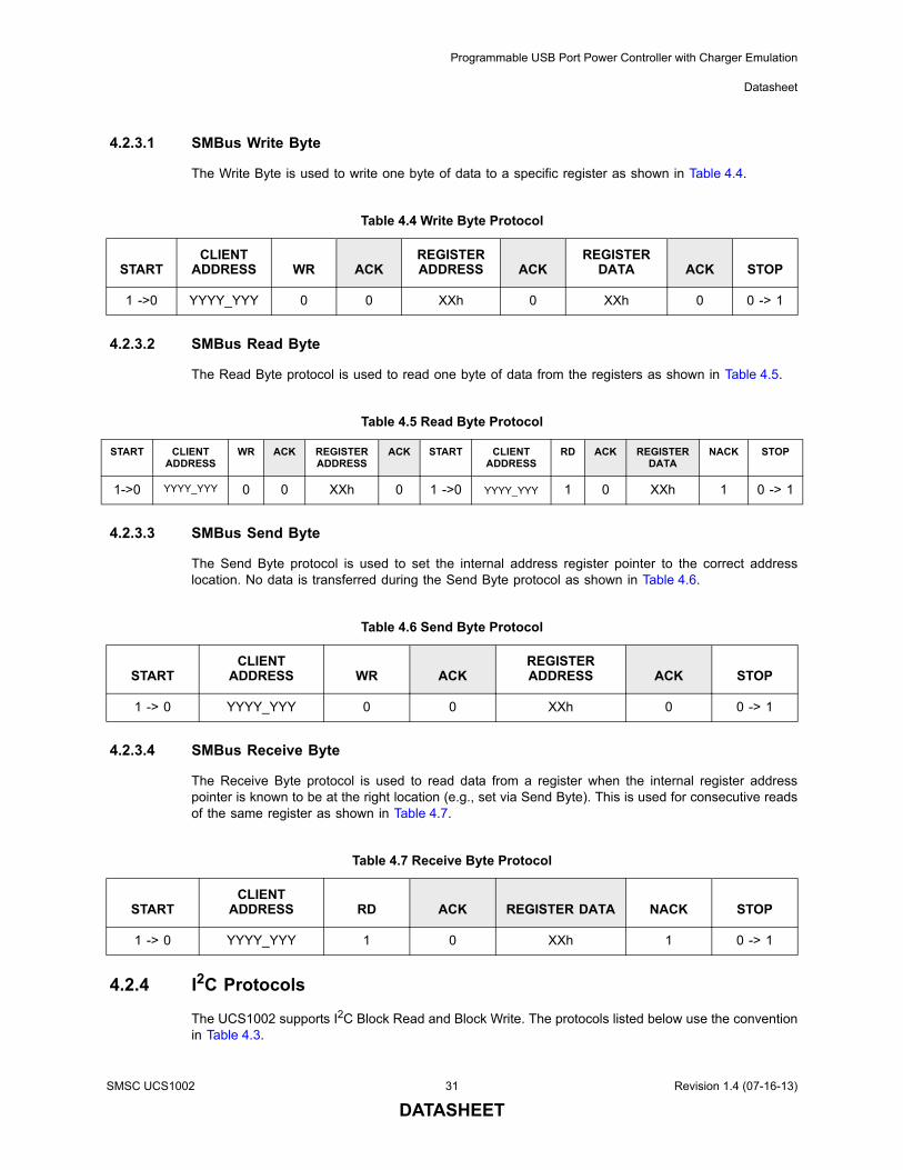
Programmable USB Port Power Controller with Charger Emulation
Datasheet
4.2.3.1 SMBus Write Byte
The Write Byte is used to write one byte of data to a specific register as shown in Table 4.4.
4.2.3.2 SMBus Read Byte
The Read Byte protocol is used to read one byte of data from the registers as shown in Table 4.5.
4.2.3.3 SMBus Send Byte
The Send Byte protocol is used to set the internal address register pointer to the correct addresslocation. No data is transferred during the Send Byte protocol as shown in Table 4.6.
4.2.3.4 SMBus Receive Byte
The Receive Byte protocol is used to read data from a register when the internal register addresspointer is known to be at the right location (e.g., set via Send Byte). This is used for consecutive readsof the same register as shown in Table 4.7.
4.2.4 I2C Protocols
The UCS1002 supports I2C Block Read and Block Write. The protocols listed below use the conventionin Table 4.3.
Table 4.4 Write Byte Protocol
STARTCLIENT
ADDRESS WR ACKREGISTER ADDRESS ACK
REGISTER DATA ACK STOP
1 ->0 YYYY_YYY 0 0 XXh 0 XXh 0 0 -> 1
Table 4.5 Read Byte Protocol
START CLIENT ADDRESS
WR ACK REGISTER ADDRESS
ACK START CLIENT ADDRESS
RD ACK REGISTER DATA
NACK STOP
1->0 YYYY_YYY 0 0 XXh 0 1 ->0 YYYY_YYY 1 0 XXh 1 0 -> 1
Table 4.6 Send Byte Protocol
STARTCLIENT
ADDRESS WR ACKREGISTER ADDRESS ACK STOP
1 -> 0 YYYY_YYY 0 0 XXh 0 0 -> 1
Table 4.7 Receive Byte Protocol
STARTCLIENT
ADDRESS RD ACK REGISTER DATA NACK STOP
1 -> 0 YYYY_YYY 1 0 XXh 1 0 -> 1
SMSC UCS1002 31 Revision 1.4 (07-16-13)
DATASHEET
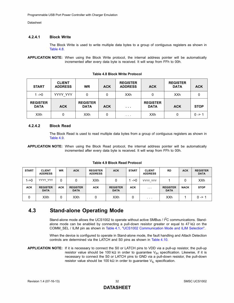
Programmable USB Port Power Controller with Charger Emulation
Datasheet
4.2.4.1 Block Write
The Block Write is used to write multiple data bytes to a group of contiguous registers as shown inTable 4.8.
APPLICATION NOTE: When using the Block Write protocol, the internal address pointer will be automaticallyincremented after every data byte is received. It will wrap from FFh to 00h.
4.2.4.2 Block Read
The Block Read is used to read multiple data bytes from a group of contiguous registers as shown inTable 4.9.
APPLICATION NOTE: When using the Block Read protocol, the internal address pointer will be automaticallyincremented after every data byte is received. It will wrap from FFh to 00h.
4.3 Stand-alone Operating Mode
Stand-alone mode allows the UCS1002 to operate without active SMBus / I2C communications. Stand-alone mode can be enabled by connecting a pull-down resistor greater or equal to 47 kΩ on theCOMM_SEL / ILIM pin as shown in Table 4.1, "UCS1002 Communication Mode and ILIM Selection".
When the device is configured to operate in Stand-alone mode, the fault handling and Attach Detectioncontrols are determined via the LATCH and S0 pins as shown in Table 4.10.
APPLICATION NOTE: If it is necessary to connect the S0 or LATCH pins to VDD via a pull-up resistor, the pull-upresistor value should be 100 kΩ in order to guarantee VIH specification. Likewise, if it isnecessary to connect the S0 or LATCH pins to GND via a pull-down resistor, the pull-downresistor value should be 100 kΩ in order to guarantee VIL specification.
Table 4.8 Block Write Protocol
STARTCLIENT
ADDRESS WR ACKREGISTER ADDRESS ACK
REGISTER DATA ACK
1 ->0 YYYY_YYY 0 0 XXh 0 XXh 0
REGISTER DATA ACK
REGISTER DATA ACK . . .
REGISTER DATA ACK STOP
XXh 0 XXh 0 . . . XXh 0 0 -> 1
Table 4.9 Block Read Protocol
START CLIENT ADDRESS
WR ACK REGISTER ADDRESS
ACK START CLIENT ADDRESS
RD ACK REGISTER DATA
1->0 YYYY_YYY 0 0 XXh 0 1 ->0 YYYY_YYY 1 0 XXh
ACK REGISTER DATA
ACK REGISTER DATA
ACK REGISTER DATA
ACK . . . REGISTER DATA
NACK STOP
0 XXh 0 XXh 0 XXh 0 . . . XXh 1 0 -> 1
Revision 1.4 (07-16-13) 32 SMSC UCS1002
DATASHEET
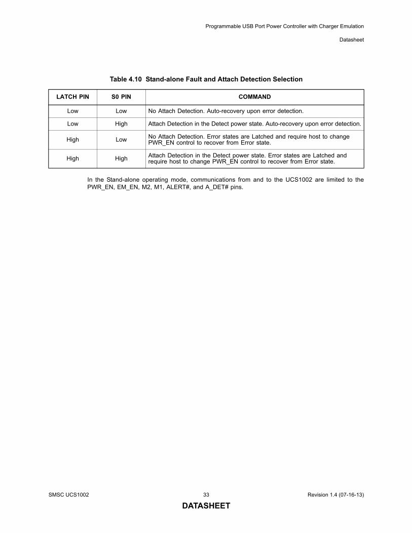
Programmable USB Port Power Controller with Charger Emulation
Datasheet
In the Stand-alone operating mode, communications from and to the UCS1002 are limited to thePWR_EN, EM_EN, M2, M1, ALERT#, and A_DET# pins.
Table 4.10 Stand-alone Fault and Attach Detection Selection
LATCH PIN S0 PIN COMMAND
Low Low No Attach Detection. Auto-recovery upon error detection.
Low High Attach Detection in the Detect power state. Auto-recovery upon error detection.
High Low No Attach Detection. Error states are Latched and require host to change PWR_EN control to recover from Error state.
High High Attach Detection in the Detect power state. Error states are Latched and require host to change PWR_EN control to recover from Error state.
SMSC UCS1002 33 Revision 1.4 (07-16-13)
DATASHEET
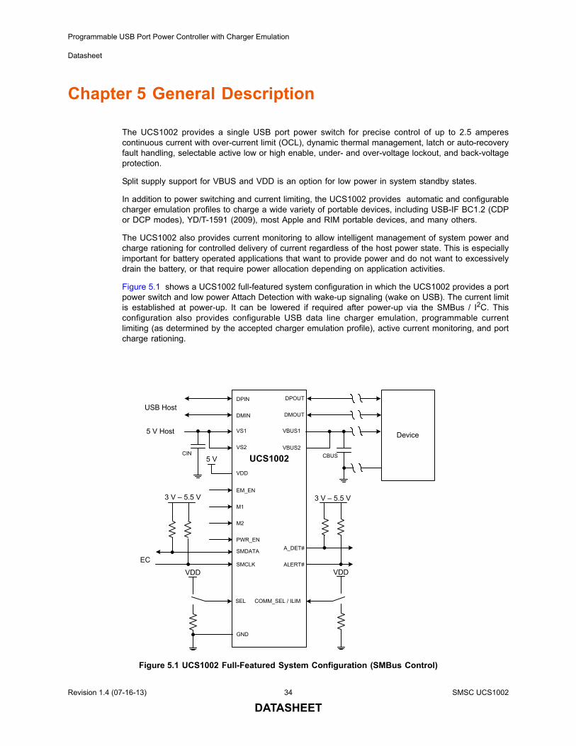
Programmable USB Port Power Controller with Charger Emulation
Datasheet
Chapter 5 General Description
The UCS1002 provides a single USB port power switch for precise control of up to 2.5 amperescontinuous current with over-current limit (OCL), dynamic thermal management, latch or auto-recoveryfault handling, selectable active low or high enable, under- and over-voltage lockout, and back-voltageprotection.
Split supply support for VBUS and VDD is an option for low power in system standby states.
In addition to power switching and current limiting, the UCS1002 provides automatic and configurablecharger emulation profiles to charge a wide variety of portable devices, including USB-IF BC1.2 (CDPor DCP modes), YD/T-1591 (2009), most Apple and RIM portable devices, and many others.
The UCS1002 also provides current monitoring to allow intelligent management of system power andcharge rationing for controlled delivery of current regardless of the host power state. This is especiallyimportant for battery operated applications that want to provide power and do not want to excessivelydrain the battery, or that require power allocation depending on application activities.
Figure 5.1 shows a UCS1002 full-featured system configuration in which the UCS1002 provides a portpower switch and low power Attach Detection with wake-up signaling (wake on USB). The current limitis established at power-up. It can be lowered if required after power-up via the SMBus / I2C. Thisconfiguration also provides configurable USB data line charger emulation, programmable currentlimiting (as determined by the accepted charger emulation profile), active current monitoring, and portcharge rationing.
Figure 5.1 UCS1002 Full-Featured System Configuration (SMBus Control)
UCS1002
ALERT#
3 V – 5.5 V
Device
DPOUT
DMOUT
5 V
VBUS1
VBUS2
VS1
VS2
A_DET#
5 V Host
CBUS
USB Host
3 V – 5.5 V
EC
CIN
VDD
DPIN
DMIN
VDD
EM_EN
M1
M2
PWR_EN
SMDATA
SMCLK
SEL COMM_SEL / ILIM
GND
VDD
Revision 1.4 (07-16-13) 34 SMSC UCS1002
DATASHEET
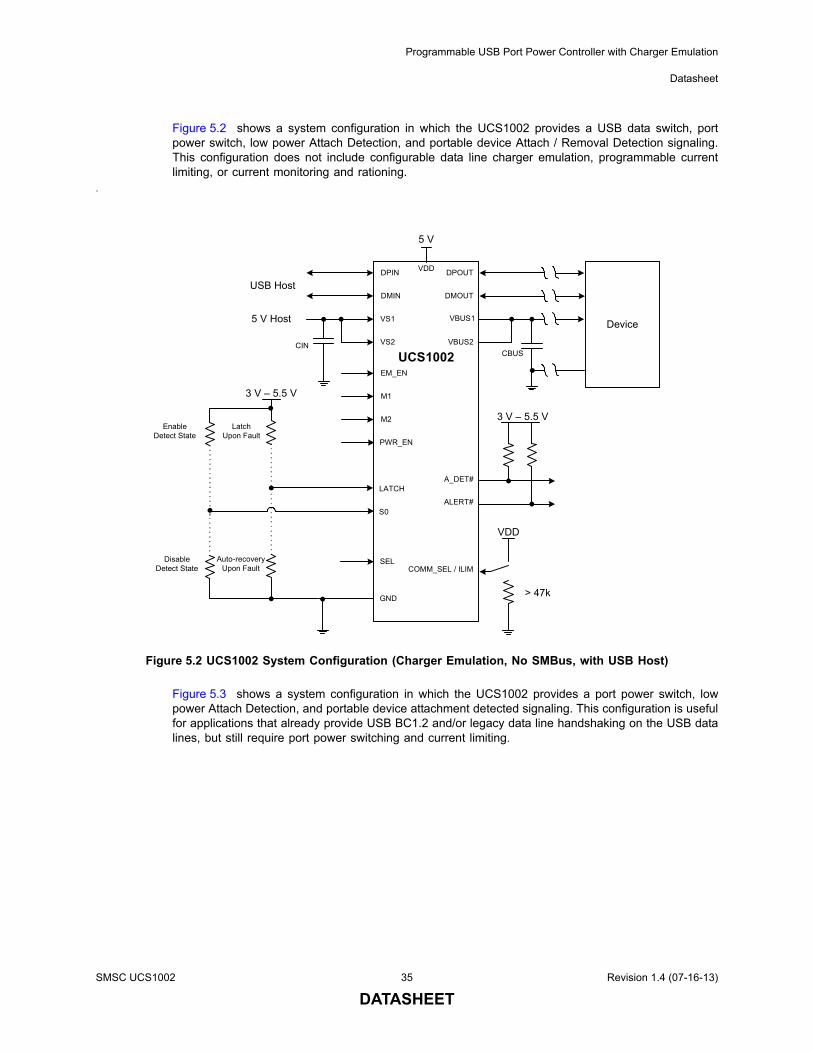
Programmable USB Port Power Controller with Charger Emulation
Datasheet
Figure 5.2 shows a system configuration in which the UCS1002 provides a USB data switch, portpower switch, low power Attach Detection, and portable device Attach / Removal Detection signaling.This configuration does not include configurable data line charger emulation, programmable currentlimiting, or current monitoring and rationing.
.
Figure 5.3 shows a system configuration in which the UCS1002 provides a port power switch, lowpower Attach Detection, and portable device attachment detected signaling. This configuration is usefulfor applications that already provide USB BC1.2 and/or legacy data line handshaking on the USB datalines, but still require port power switching and current limiting.
Figure 5.2 UCS1002 System Configuration (Charger Emulation, No SMBus, with USB Host)
UCS1002
LATCH
ALERT#
PWR_EN
3 V – 5.5 V
GND
Device
DPIN
DMIN
DPOUT
DMOUT
VDD
5 V
VBUS1
VBUS2
VS1
VS2
COMM_SEL / ILIM
3 V – 5.5 V
Auto-recovery Upon Fault
Latch Upon Fault
EM_EN
M1
M2
SEL
A_DET#
5 V Host
CBUS
USB Host
S0
Disable Detect State
Enable Detect State
CIN
VDD
> 47k
SMSC UCS1002 35 Revision 1.4 (07-16-13)
DATASHEET
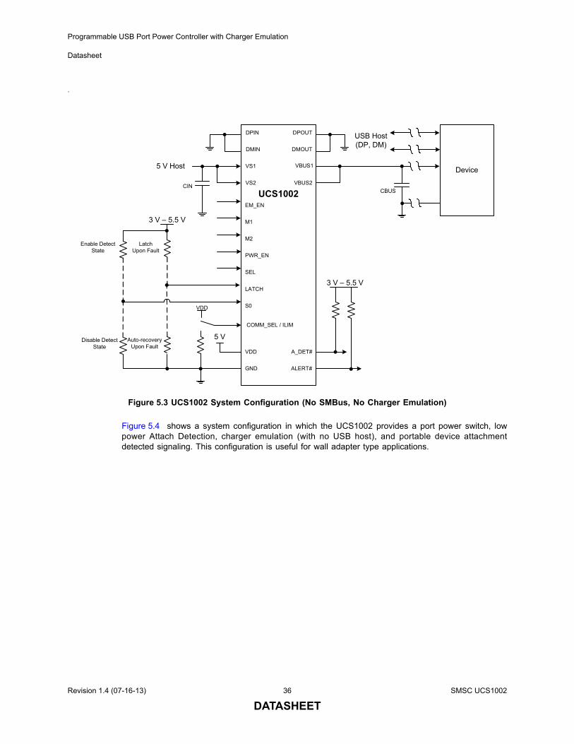
Programmable USB Port Power Controller with Charger Emulation
Datasheet
.
Figure 5.4 shows a system configuration in which the UCS1002 provides a port power switch, lowpower Attach Detection, charger emulation (with no USB host), and portable device attachmentdetected signaling. This configuration is useful for wall adapter type applications.
Figure 5.3 UCS1002 System Configuration (No SMBus, No Charger Emulation)
UCS1002
LATCH
ALERT#
PWR_EN
3 V – 5.5 V
GND
Device
DPIN
DMIN
DPOUT
DMOUT
VDD
5 V
VBUS1
VBUS2
VS1
VS2
COMM_SEL / ILIM
3 V – 5.5 V
Auto-recovery Upon Fault
Latch Upon Fault
EM_EN
M1
M2
SEL
A_DET#
5 V Host
CBUS
USB Host (DP, DM)
S0
Disable Detect State
Enable Detect State
CIN
VDD
Revision 1.4 (07-16-13) 36 SMSC UCS1002
DATASHEET
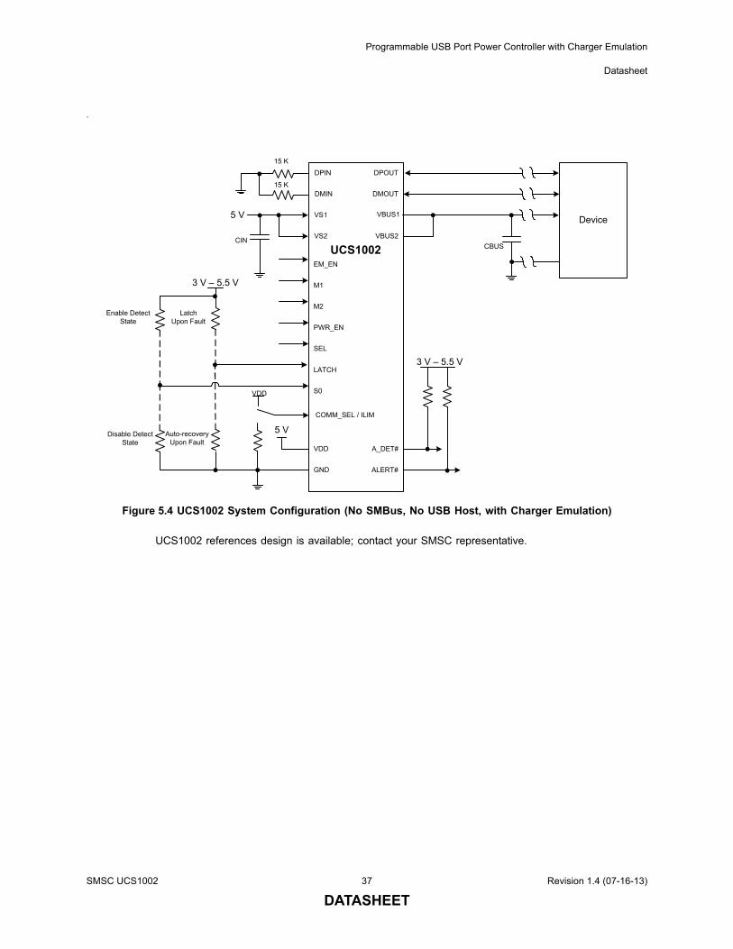
Programmable USB Port Power Controller with Charger Emulation
Datasheet
.
UCS1002 references design is available; contact your SMSC representative.
Figure 5.4 UCS1002 System Configuration (No SMBus, No USB Host, with Charger Emulation)
UCS1002
LATCH
ALERT#
PWR_EN
3 V – 5.5 V
GND
Device
DPIN
DMIN
DPOUT
DMOUT
VDD
5 V
VBUS1
VBUS2
VS1
VS2
COMM_SEL / ILIM
3 V – 5.5 V
Auto-recovery Upon Fault
Latch Upon Fault
EM_EN
M1
M2
SEL
A_DET#
5 V
CBUS
S0
Disable Detect State
Enable Detect State
CIN
VDD
15 K
15 K
SMSC UCS1002 37 Revision 1.4 (07-16-13)
DATASHEET
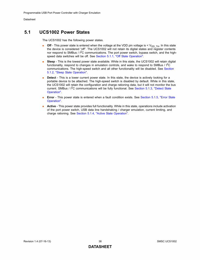
Programmable USB Port Power Controller with Charger Emulation
Datasheet
5.1 UCS1002 Power States
The UCS1002 has the following power states.
Off - This power state is entered when the voltage at the VDD pin voltage is < VDD_TH. In this state the device is considered “off”. The UCS1002 will not retain its digital states and register contents nor respond to SMBus / I2C communications. The port power switch, bypass switch, and the high-speed data switches will be off. See Section 5.1.1, "Off State Operation".
Sleep - This is the lowest power state available. While in this state, the UCS1002 will retain digital functionality, respond to changes in emulation controls, and wake to respond to SMBus / I2C communications. The high-speed switch and all other functionality will be disabled. See Section 5.1.2, "Sleep State Operation".
Detect - This is a lower current power state. In this state, the device is actively looking for a portable device to be attached. The high-speed switch is disabled by default. While in this state, the UCS1002 will retain the configuration and charge rationing data, but it will not monitor the bus current. SMBus / I2C communications will be fully functional. See Section 5.1.3, "Detect State Operation".
Error - This power state is entered when a fault condition exists. See Section 5.1.5, "Error State Operation".
Active - This power state provides full functionality. While in this state, operations include activation of the port power switch, USB data line handshaking / charger emulation, current limiting, and charge rationing. See Section 5.1.4, "Active State Operation".
Revision 1.4 (07-16-13) 38 SMSC UCS1002
DATASHEET
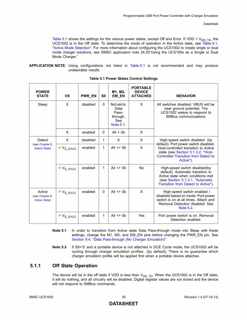
Programmable USB Port Power Controller with Charger Emulation
Datasheet
Table 5.1 shows the settings for the various power states, except Off and Error. If VDD < VDD_TH, theUCS1002 is in the Off state. To determine the mode of operation in the Active state, see Table 9.1,"Active Mode Selection". For more information about configuring the UCS1002 to create single or dualmode charger solutions, see SMSC application note 24.20“Using the UCS100x as a Single or DualMode Charger.”
APPLICATION NOTE: Using configurations not listed in Table 5.1 is not recommended and may produceundesirable results.
Note 5.1 In order to transition from Active state Data Pass-through mode into Sleep with thesesettings, change the M1, M2, and EM_EN pins before changing the PWR_EN pin. SeeSection 9.4, "Data Pass-through (No Charger Emulation)".
Note 5.2 If S0=’0’ and a portable device is not attached in DCE Cycle mode, the UCS1002 will becycling through charger emulation profiles (by default). There is no guarantee whichcharger emulation profile will be applied first when a portable device attaches.
5.1.1 Off State Operation
The device will be in the off state if VDD is less than VDD_TH. When the UCS1002 is in the Off state,it will do nothing, and all circuitry will be disabled. Digital register values are not stored and the devicewill not respond to SMBus commands.
Table 5.1 Power States Control Settings
POWER STATE VS PWR_EN S0
M1, M2, EM_EN
PORTABLE DEVICE
ATTACHED BEHAVIOR
Sleep X disabled 0 Not set to Data Pass-
through. See
Note 5.1.
X All switches disabled. VBUS will be near ground potential. The
UCS1002 wakes to respond to SMBus communications.
X enabled 0 All = 0b X
Detect(see Chapter 8,
Detect State)
X disabled 1 X X High-speed switch disabled (by default). Port power switch disabled. Host-controlled transition to Active state (see Section 5.1.3.2, "Host-
Controlled Transition from Detect to Active").
< VS_UVLO enabled 1 All <> 0b X
> VS_UVLO enabled 1 All <> 0b No High-speed switch disabled(by default). Automatic transition to
Active state when conditions met (see Section 5.1.3.1, "Automatic
Transition from Detect to Active").
Active(see Chapter 9,
Active State)
> VS_UVLO enabled 0 All <> 0b X High-speed switch enabled / disabled based on mode. Port power switch is on at all times. Attach and Removal Detection disabled. See
Note 5.2.
> VS_UVLO enabled 1 All <> 0b Yes Port power switch is on. Removal Detection enabled.
SMSC UCS1002 39 Revision 1.4 (07-16-13)
DATASHEET
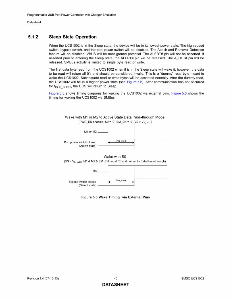
Programmable USB Port Power Controller with Charger Emulation
Datasheet
5.1.2 Sleep State Operation
When the UCS1002 is in the Sleep state, the device will be in its lowest power state. The high-speedswitch, bypass switch, and the port power switch will be disabled. The Attach and Removal Detectionfeature will be disabled. VBUS will be near ground potential. The ALERT# pin will not be asserted. Ifasserted prior to entering the Sleep state, the ALERT# pin will be released. The A_DET# pin will bereleased. SMBus activity is limited to single byte read or write.
The first data byte read from the UCS1002 when it is in the Sleep state will wake it; however, the datato be read will return all 0’s and should be considered invalid. This is a “dummy” read byte meant towake the UCS1002. Subsequent read or write bytes will be accepted normally. After the dummy read,the UCS1002 will be in a higher power state (see Figure 5.6). After communication has not occurredfor tIDLE_SLEEP, the UCS will return to Sleep.
Figure 5.5 shows timing diagrams for waking the UCS1002 via external pins. Figure 5.6 shows thetiming for waking the UCS1002 via SMBus.
Figure 5.5 Wake Timing via External Pins
M1 or M2
Port power switch closed (Active state)
tPIN_WAKE
Wake with M1 or M2 to Active State Data Pass-through Mode(PWR_EN enabled, S0 = ‘0’, EM_EN = ‘0’, VS > VS_UVLO)
S0
Bypass switch closed (Detect state)
tPIN_WAKE
Wake with S0(VS > VS_UVLO, M1 & M2 & EM_EN not all ‘0’ and not set to Data Pass-through)
Revision 1.4 (07-16-13) 40 SMSC UCS1002
DATASHEET
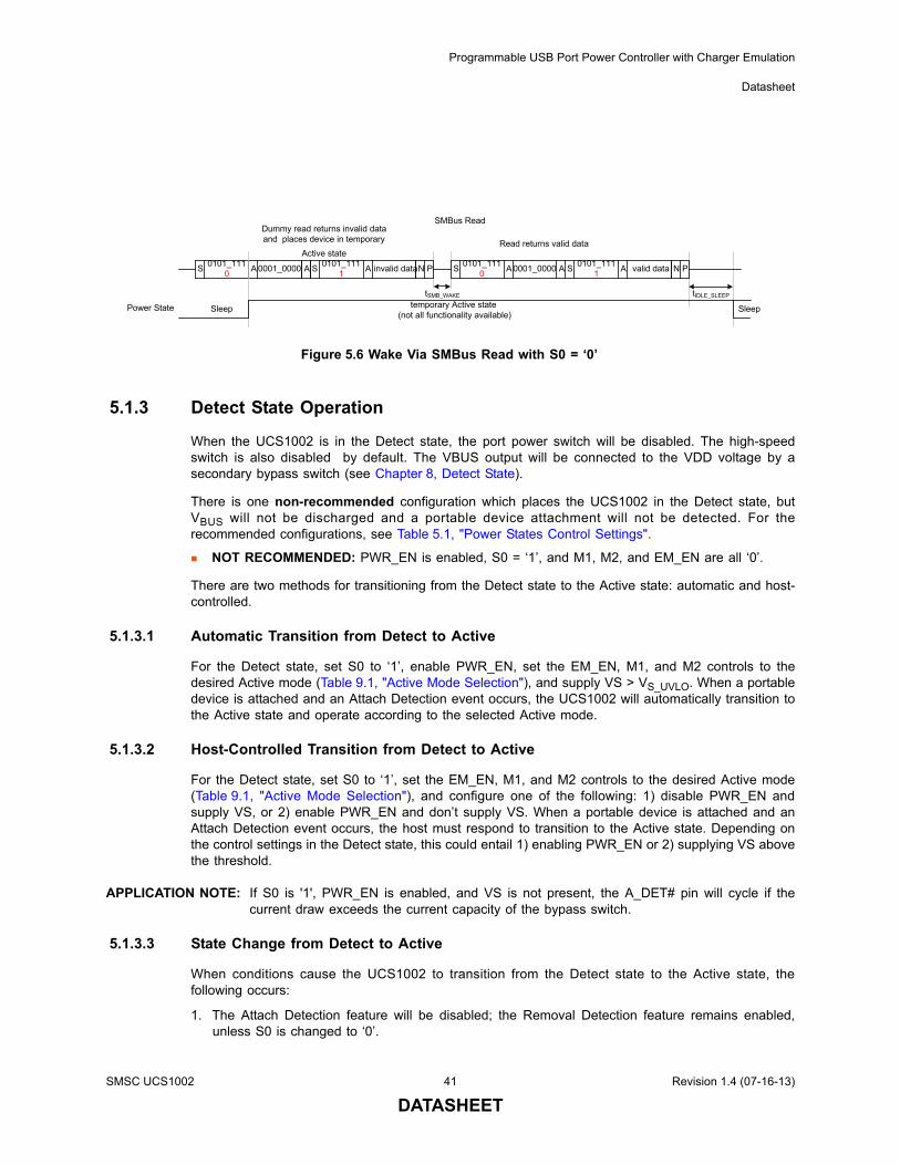
Programmable USB Port Power Controller with Charger Emulation
Datasheet
5.1.3 Detect State Operation
When the UCS1002 is in the Detect state, the port power switch will be disabled. The high-speedswitch is also disabled by default. The VBUS output will be connected to the VDD voltage by asecondary bypass switch (see Chapter 8, Detect State).
There is one non-recommended configuration which places the UCS1002 in the Detect state, butVBUS will not be discharged and a portable device attachment will not be detected. For therecommended configurations, see Table 5.1, "Power States Control Settings".
NOT RECOMMENDED: PWR_EN is enabled, S0 = ‘1’, and M1, M2, and EM_EN are all ‘0’.
There are two methods for transitioning from the Detect state to the Active state: automatic and host-controlled.
5.1.3.1 Automatic Transition from Detect to Active
For the Detect state, set S0 to ‘1’, enable PWR_EN, set the EM_EN, M1, and M2 controls to thedesired Active mode (Table 9.1, "Active Mode Selection"), and supply VS > VS_UVLO. When a portabledevice is attached and an Attach Detection event occurs, the UCS1002 will automatically transition tothe Active state and operate according to the selected Active mode.
5.1.3.2 Host-Controlled Transition from Detect to Active
For the Detect state, set S0 to ‘1’, set the EM_EN, M1, and M2 controls to the desired Active mode(Table 9.1, "Active Mode Selection"), and configure one of the following: 1) disable PWR_EN andsupply VS, or 2) enable PWR_EN and don’t supply VS. When a portable device is attached and anAttach Detection event occurs, the host must respond to transition to the Active state. Depending onthe control settings in the Detect state, this could entail 1) enabling PWR_EN or 2) supplying VS abovethe threshold.
APPLICATION NOTE: If S0 is '1', PWR_EN is enabled, and VS is not present, the A_DET# pin will cycle if thecurrent draw exceeds the current capacity of the bypass switch.
5.1.3.3 State Change from Detect to Active
When conditions cause the UCS1002 to transition from the Detect state to the Active state, thefollowing occurs:
1. The Attach Detection feature will be disabled; the Removal Detection feature remains enabled,unless S0 is changed to ‘0’.
Figure 5.6 Wake Via SMBus Read with S0 = ‘0’
0101_1110
A invalid dataN P
SMBus Read
A0001_00000101_111
0A valid data N P0001_0000SS
tIDLE_SLEEP
Sleep Sleep
Dummy read returns invalid data and places device in temporary
Active state Read returns valid data
0101_1111
AS0101_111
1ASA
Power State temporary Active state (not all functionality available)
tSMB_WAKE
SMSC UCS1002 41 Revision 1.4 (07-16-13)
DATASHEET
Programmable USB Port Power Controller with Charger Emulation
Datasheet
2. The bypass switch will be turned off.
3. The discharge switch will be turned on for tDISCHARGE.
4. The port power switch will be turned on.
5.1.4 Active State Operation
Every time that the UCS1002 enters the Active state and the port power switch is closed, it will enterthe mode as instructed by the host controller (see Chapter 9, Active State). The UCS1002 cannot bein the Active state (and therefore, the port power switch cannot be turned on) if any of the followingconditions exist:
1. VS < VS_UVLO.
2. PWR_EN is disabled.
3. M1, M2, and EM_EN are all set to '0'.
4. S0 is set to ‘1’ and an Attach Detection event has not occurred.
Revision 1.4 (07-16-13) 42 SMSC UCS1002
DATASHEET
Programmable USB Port Power Controller with Charger Emulation
Datasheet
5.1.5 Error State Operation
The UCS1002 will enter the Error state from the Active state when any of the following events aredetected:
1. The maximum allowable internal die temperature (TTSD) has been exceeded (see Section 7.3.1.2).
2. An over-current condition has been detected (see Section 7.2.1).
3. An under-voltage condition on VBUS has been detected (see Section 5.2.5).
4. A back-drive condition has been detected (see Section 5.2.3).
5. A discharge error has been detected (see Section 7.4).
6. An over-voltage condition on the VS pins.
The UCS1002 will enter the Error state from the Detect state when a back-drive condition has beendetected or when the maximum allowable internal die temperature has been exceeded.
The UCS1002 will enter the Error state from the Sleep state when a back-drive condition has beendetected.
When the UCS1002 enters the Error state, the port power switch, the VBUS bypass switch, the high-speed switch are turned off, and the ALERT# pin is asserted (by default). They will remain off while inthis power state. The UCS1002 will leave this state as determined by the fault handling selection (seeSection 7.6, "Fault Handling Mechanism").
When using the Latch fault handler and the user has re-activated the device by clearing the ERR bit(see Section 10.3, "Status Registers"), or toggling the PWR_EN control, the UCS1002 will check thatall of the error conditions have been removed. If using Auto-recovery fault handler, after the tCYCLEtime period, the UCS1002 will check that all of the error conditions have been removed.
If all of the error conditions have been removed, the UCS1002 will return to the Active state or Detectstate, as applicable. Returning to the Active state will cause the UCS1002 to restart the selected mode(see Section 9.2, "Active Mode Selection").
If the device is in the Error state and a Removal Detection event occurs, it will check the errorconditions and then return to the power state defined by the PWR_EN, M1, M2, EM_EN, and S0controls.
5.2 Supply Voltages
5.2.1 VDD Supply Voltage
The UCS1002 requires 4.5 V to 5.5 V present on the VDD pin for core device functionality. Core devicefunctionality consists of maintaining register states, wake-up upon SMBus / I2C query, and AttachDetection.
5.2.2 VS Source Voltage
VS can be a separate supply and can be greater than VDD to accommodate high current applicationsin which current path resistances result in unacceptable voltage drops that may prevent optimalcharging of some portable devices.
SMSC UCS1002 43 Revision 1.4 (07-16-13)
DATASHEET
Programmable USB Port Power Controller with Charger Emulation
Datasheet
5.2.3 Back-voltage Detection
Whenever the following conditions are true, the port power switch will be disabled, the VBUS bypassswitch will be disabled, the high-speed data switch will be disabled, and a Back-voltage event will beflagged. This will cause the UCS1002 to enter the Error power state (see Section 5.1.5, "Error StateOperation").
1. The VBUS voltage exceeds the VS voltage by VBV_TH and the port power switch is closed. Theport power switch will be opened immediately. If the condition lasts for longer than tMASK, then theUCS1002 will enter the Error state. Otherwise, the port power switch will be turned on as soon asthe condition is removed.
2. The VBUS voltage exceeds the VDD voltage by VBV_TH and the VBUS bypass switch is closed.The bypass switch will be opened immediately. If the condition lasts for longer than tMASK, then theUCS1002 will enter the Error state. Otherwise, the bypass switch will be turned on as soon as thecondition is removed.
5.2.4 Back-drive Current Protection
If a portable device is attached that is self-powered, it may drive the VBUS port to its power supplyvoltage level; however, the UCS1002 is designed such that leakage current from the VBUS pins to theVDD or VS pins shall not exceed IBD_1 (if the VDD voltage is zero) or IBD_2 (if the VDD voltage exceedsVDD_TH).
5.2.5 Under-voltage Lockout on VS
The UCS1002 requires a minimum voltage (VS_UVLO) be present on the VS pin for Active power state.
5.2.6 Over-voltage Detection and Lockout on VS
The UCS1002 port power switch will be disabled if the voltage on the VS pin exceeds a voltage(VS_OV) for longer than the specified time (tMASK). This will cause the device to enter the Error state.
5.3 Discrete Input Pins
APPLICATION NOTE: If it is necessary to connect any of the control pins except the COMM_SEL / ILIM or SELpins via a resistor to VDD or GND, the resistor value should not exceed 100 kΩ in order tomeet the VIH and VIL specifications.
5.3.1 COMM_SEL / ILIM Input
The COMM_SEL / ILIM input determines the initial ILIM settings and the communications mode, asshown in Table 4.1, "UCS1002 Communication Mode and ILIM Selection".
5.3.2 SEL Input
The SEL pin selects the polarity of the PWR_EN control. In addition, if the UCS1002 is not configuredto operate in Stand-alone mode, the SEL pin determines the SMBus address. See Table 4.2, "SEL PinDecode". The SEL pin state is latched upon device power-up and further changes will have no effect.
Revision 1.4 (07-16-13) 44 SMSC UCS1002
DATASHEET

Programmable USB Port Power Controller with Charger Emulation
Datasheet
5.3.3 M1, M2, and EM_EN Inputs
The M1, M2, and EM_EN input controls determine the Active mode and affect the power state (seeTable 5.1, "Power States Control Settings" and Table 9.1, "Active Mode Selection"). When thesecontrols are all set to ‘0’ and PWR_EN is enabled, the UCS1002 Attach and Removal Detection featureis disabled. In SMBus mode, the M1, M2, and EM_EN pin states will be ignored by the UCS1002 ifthe PIN_IGNORE configuration bit is set (see Section 10.4.3); otherwise, the M1_SET, M2_SET, andEM_EN_SET configuration bits (see Section 10.4.3) are checked along with the pins.
5.3.4 PWR_EN Input
The PWR_EN control enables the port power switch to be turned on if conditions are met and affectsthe power state (see Table 5.1, "Power States Control Settings"). The port power switch cannot beclosed if PWR_EN is disabled. However, if PWR_EN is enabled, the port power switch is notnecessarily closed (see Section 5.1.4, "Active State Operation"). Polarity is controlled by the SEL pin.In SMBus mode, the PWR_EN pin state will be ignored by the UCS1002 if the PIN_IGNOREconfiguration bit is set (see Section 10.4.3); otherwise, the PWR_EN_SET configuration bit (seeSection 10.4.3) is checked along with the pin.
5.3.5 Latch Input
The Latch input control determines the behavior of the fault handling mechanism (see Section 7.6,"Fault Handling Mechanism").
When the UCS1002 is configured to operate in Stand-alone mode (see Section 4.3, "Stand-aloneOperating Mode"), the LATCH control is available exclusively via the LATCH pin (see SectionTable 4.10, "Stand-alone Fault and Attach Detection Selection"). When the UCS1002 is configured tooperate in SMBus mode, the LATCH control is available exclusively via the LATCH_SET configurationbit (see Section 10.4.3, "Switch Configuration - 17h").
5.3.6 S0 Input
The S0 control enables the Attach and Removal Detection feature and affects the power state (seeTable 5.1, "Power States Control Settings"). When S0 is set to ‘1’, an Attach Detection event mustoccur before the port power switch can be turned on. When S0 is set to ‘0’, the Attach and RemovalDetection feature is not enabled.
When the device is configured to operate in SMBus mode, (see Section 4.3, "Stand-alone OperatingMode"), the S0 control is available exclusively via the S0_SET configuration bit (see Section 10.4.3,"Switch Configuration - 17h"). Otherwise, the S0 control is available exclusively via the S0 pin sincethe SMBus protocol will be disabled.
5.4 Discrete Output Pins
5.4.1 ALERT# and A_DET# Output Pins
The ALERT# pin is an active low open-drain interrupt to the host controller. The ALERT# pin isasserted (by default - see ALERT_MASK in Section 10.4.1, "General Configuration - 15h") when anerror occurs (see Section 10.3.2, "Interrupt Status - 10h"). The ALERT# pin can also be asserted whenthe LOW_CUR (portable device is pulling less current and may be finished charging) or TREG (thermalregulation temperature exceeded) bits are set and linked. As well, when charge rationing is enabled,the ALERT# pin is asserted by default when the current rationing threshold is reached (as determinedby RATION_BEH[1:0] - see Table 7.1, "Charge Rationing Behavior"). The ALERT# pin is releasedwhen all conditions that may assert the ALERT# pin (such as an error condition, charge rationing, andTREG and LOW_CHG if linked) have been removed or reset as necessary.
SMSC UCS1002 45 Revision 1.4 (07-16-13)
DATASHEET
Programmable USB Port Power Controller with Charger Emulation
Datasheet
The A_DET# pinprovides an active low open-drain output indication that a valid Attach Detection eventhas occurred. It will remain asserted until the UCS1002 is placed into the Sleep state or a RemovalDetection event occurs. For wake on USB, the A_DET# pin assertion can be utilized by the system.If the S0 control is ‘0’ and the UCS1002 is in the Active state, the A_DET# pin will be assertedregardless if a portable device is attached or not. If S0 is '1', PWR_EN is enabled, and VS is notpresent, the A_DET# pin will cycle if the current draw exceeds the current capacity of the bypassswitch.
5.4.2 Interrupt Blanking
The ALERT# and A_DET# pins will not be asserted for a specified time (up to tBLANK) after power-up.Additionally, an error condition (except for the thermal shutdown) must be present for longer than aspecified time (tMASK) before the ALERT# pin is asserted.
Revision 1.4 (07-16-13) 46 SMSC UCS1002
DATASHEET
Programmable USB Port Power Controller with Charger Emulation
Datasheet
SMSC UCS1002 47 Revision 1.4 (07-16-13)
DATASHEET
Chapter 6 USB High-speed Data Switch
6.1 USB High-speed Data Switch
The UCS1002 contains a series USB 2.0 compliant high-speed switch between the DPIN and DMINpins and between the DPOUT and DMOUT pins. This switch is designed for high-speed, low latencyfunctionality to allow USB 2.0 full-speed and high-speed communications with minimal interference.
Nominally, the switch is closed in the Active state, allowing uninterrupted USB communicationsbetween the upstream host and the portable device. The switch is opened when:
1. The UCS1002 is actively emulating using any of the charger emulation profiles except CDP (bydefault - see Section 10.4.5, "High-speed Switch Configuration - 25h").
2. The UCS1002 is operating as a dedicated charger unless the HSW_DCE configuration bit is set(see Section 10.4.5).
3. The UCS1002 is in the Detect state (by default) or in the Sleep state.
APPLICATION NOTE: If the VDD voltage is less than VDD_TH, the high-speed data switch will be disabled andopened.
6.1.1 USB-IF High-speed Compliance
The USB data switch will not significantly degrade the signal integrity through the device DP / DM pinswith USB high-speed communications.
Programmable USB Port Power Controller with Charger Emulation
Datasheet
Chapter 7 USB Port Power Switch
7.1 USB Port Power Switch
To assure compliance to various charging specifications, the UCS1002 contains a USB port powerswitch that supports two current limiting modes: trip and constant current (variable slope). The currentlimit (ILIM) is pin selectable (and may be updated via the register set). The switch also includes softstart circuitry and a separate short circuit current limit.
The port power switch is on in the Active state (except when VBUS is discharging).
7.2 Current Limiting
7.2.1 Current Limit Setting
The UCS1002 hardware set current limit, ILIM, can be one of eight values (see Table 4.1, "UCS1002Communication Mode and ILIM Selection"). This resistor value is read once upon UCS1002 power-up.The current limit can be changed via the SMBus / I2C after power-up; however, the programmedcurrent limit cannot exceed the hardware set current limit.
At power-up, the communication mode (Stand-alone or SMBus / I2C) and hardware current limit (ILIM)are determined via the pull-down resistor (or pull-up resistor if connected to VDD) on the COMM_SEL/ ILIM pin, as shown in Table 4.1.
7.2.2 Short Circuit Output Current Limiting
Short circuit current limiting occurs when the output current is above the selectable current limit (ILIMx).This event will be detected and the current will immediately be limited (within tSHORT_LIM time). If thecondition remains, the port power switch will flag an Error condition and enter the Error state (seeSection 5.1.5, "Error State Operation").
7.2.3 Soft Start
When the PWR_EN control changes states to enable the port power switch, or an Attach Detectionevent occurs in the Detect power state and the PWR_EN control is already enabled, the UCS1002invokes a soft start routine for the duration of the VBUS rise time (tR_BUS). This soft start routine willlimit current flow from VS into VBUS while it is active. This circuitry will prevent current spikes due toa step in the portable device current draw.
In the case when a portable device is attached while the PWR_EN pin is already enabled, if the buscurrent exceeds ILIM, the UCS1002 current limiter will respond within a specified time (tSHORT_LIM)and will operate normally at this point. The CBUS capacitor will deliver the extra current, if any, asrequired by the load change.
7.2.4 Current Limiting Modes
The UCS1002 current limiting has two modes: trip and constant current (variable slope). Either modefunctions at all times when the port power switch is closed. The current limiting mode used dependson the Active state mode (see Section 9.9, "Current Limit Mode Associations"). When operating in theDetect power state (see Section 5.1.3), the current capacity at VBUS is limited to IBUS_BYP asdescribed in Section 8.2, "VBUS Bypass Switch".
Revision 1.4 (07-16-13) 48 SMSC UCS1002
DATASHEET
Programmable USB Port Power Controller with Charger Emulation
Datasheet
7.2.4.1 Trip Mode
When using trip current limiting, the UCS1002 USB port power switch functions as a low resistanceswitch and rapidly turns off if the current limit is exceeded. While operating using trip current limiting,the VBUS output voltage will be held relatively constant (equal to the VS voltage minus the RON * IBUScurrent) for all current values up to the ILIM.
If the current drawn by a portable device exceeds ILIM, the following occurs:
1. The port power switch will be turned off (trip action).
2. The UCS1002 will enter the Error state and assert the ALERT# pin.
3. The fault handling circuitry will then determine subsequent actions.
Trip current limiting is used by default when the UCS1002 is in Data Pass-through and DedicatedCharger Emulation Cycle (except when the BC1.2 DCP charger emulation profile is accepted), andwhen there’s no handshake.
APPLICATION NOTE: To avoid cycling in trip mode, set ILIM higher than the highest expected portable devicecurrent draw.
Figure 7.1 shows operation of current limits in trip mode with the shaded area representing the USB2.0 specified VBUS range. Dashed lines indicate the port power switch output will go to zero (e.g., trip)when ILIM is exceeded. Note that operation at all possible values of ILIM are shown in Figure 7.1 forillustrative purposes only; in actual operation only one ILIM can be active at any time.
SMSC UCS1002 49 Revision 1.4 (07-16-13)
DATASHEET
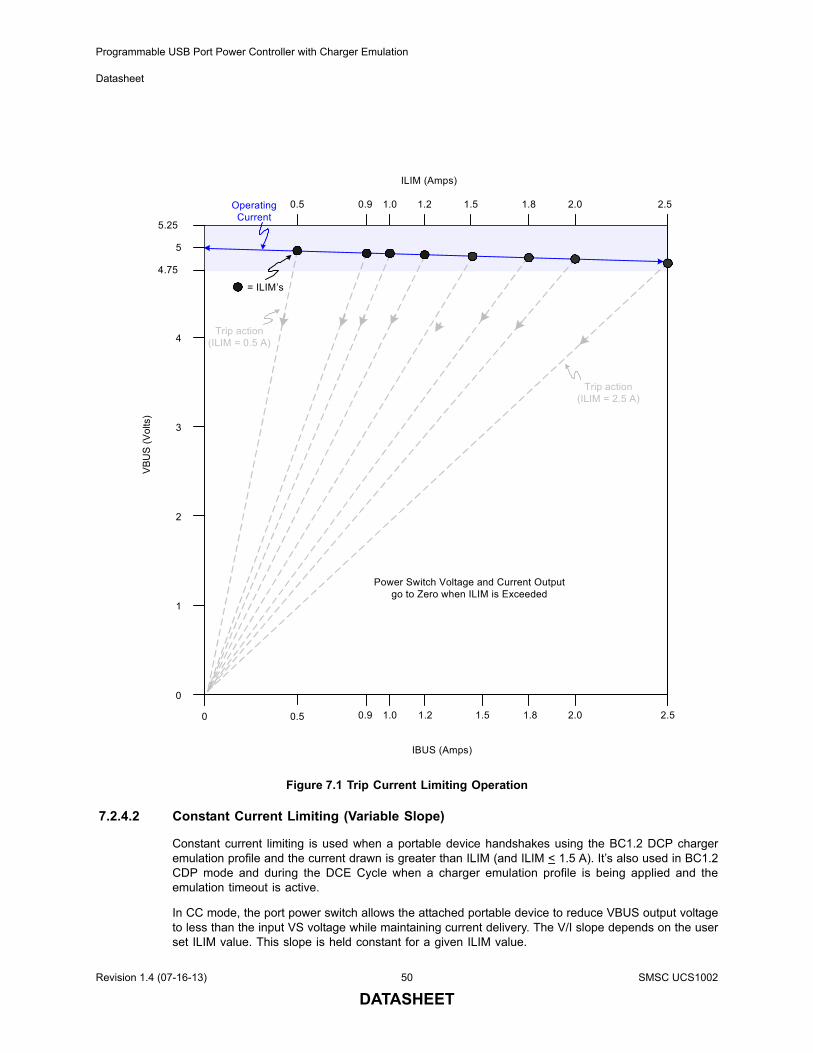
Programmable USB Port Power Controller with Charger Emulation
Datasheet
7.2.4.2 Constant Current Limiting (Variable Slope)
Constant current limiting is used when a portable device handshakes using the BC1.2 DCP chargeremulation profile and the current drawn is greater than ILIM (and ILIM < 1.5 A). It’s also used in BC1.2CDP mode and during the DCE Cycle when a charger emulation profile is being applied and theemulation timeout is active.
In CC mode, the port power switch allows the attached portable device to reduce VBUS output voltageto less than the input VS voltage while maintaining current delivery. The V/I slope depends on the userset ILIM value. This slope is held constant for a given ILIM value.
Figure 7.1 Trip Current Limiting Operation
5
4
3
2
1
0.5 1.0 1.5 2.0 2.5
5.25
4.75
IBUS (Amps)
VB
US
(V
olts
)
Operating Current
0
0
0.9 1.2
1.21.00.90.5 1.5 2.51.8 2.0
= ILIM’s
1.8
Power Switch Voltage and Current Output go to Zero when ILIM is Exceeded
Trip action (ILIM = 0.5 A)
Trip action (ILIM = 2.5 A)
ILIM (Amps)
Revision 1.4 (07-16-13) 50 SMSC UCS1002
DATASHEET
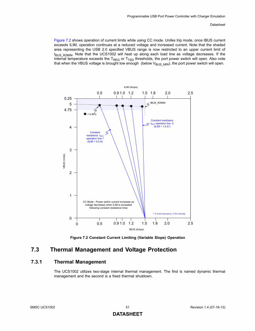
Programmable USB Port Power Controller with Charger Emulation
Datasheet
Figure 7.2 shows operation of current limits while using CC mode. Unlike trip mode, once IBUS currentexceeds ILIM, operation continues at a reduced voltage and increased current. Note that the shadedarea representing the USB 2.0 specified VBUS range is now restricted to an upper current limit ofIBUS_R2MIN. Note that the UCS1002 will heat up along each load line as voltage decreases. If theinternal temperature exceeds the TREG or TTSD thresholds, the port power switch will open. Also notethat when the VBUS voltage is brought low enough (below VBUS_MIN), the port power switch will open.
7.3 Thermal Management and Voltage Protection
7.3.1 Thermal Management
The UCS1002 utilizes two-stage internal thermal management. The first is named dynamic thermalmanagement and the second is a fixed thermal shutdown.
Figure 7.2 Constant Current Limiting (Variable Slope) Operation
5
4
3
2
1
0.5 1.0 1.5 2.0 2.5
5.25
4.75
0
00.9 1.2
1.21.00.90.5 1.5
IBUS_R2MIN
1.8
1.8 2.0 2.5
IBUS (Amps)
VB
US
(V
olts
)
ILIM (Amps)
= ILIM’s
Constant resistance IBUS operation line 1 (ILIM = 0.5 A)
Constant resistance IBUS operation line 5
(ILIM = 1.5 A*)
CC Mode - Power switch current increases as voltage decreases when ILIM is exceeded
following constant resistance lines
*1.5 A limit reduced by -3.5% internally
SMSC UCS1002 51 Revision 1.4 (07-16-13)
DATASHEET
Programmable USB Port Power Controller with Charger Emulation
Datasheet
7.3.1.1 Dynamic Thermal Management
For the first stage (active in both current limiting modes), referred to as dynamic thermal management,the UCS1002 automatically adjusts port power switch limits and modes to lower power dissipationwhen the thermal regulation temperature value is approached, as described below.
If the internal temperature exceeds the TREG value, the port power switch is opened, the current limit(ILIM) will be lowered by one step and a timer is started (tDC_TEMP). When this timer expires, the portpower switch is closed and the internal temperature will be checked again. If it remains above the TREGthreshold, the UCS1002 will repeat this cycle (open port power switch and reduce the ILIM setting byone step) until ILIM reaches its minimum value.
APPLICATION NOTE: If the temperature exceeds the TREG threshold while operating in the DCE Cycle mode aftera charger emulation profile has been accepted, the profile will be removed. The UCS1002will not restart the DCE Cycle until one of the control inputs changes states to restartemulation.
APPLICATION NOTE: The UCS1002 will not actively discharge VBUS as a result of the temperature exceedingTREG; however, any load current provided by a portable device or other load will causeVBUS to be discharged when the port power switch is opened, possibly resulting in anattached portable device resetting.
If the UCS1002 is operating using constant current limiting (variable slope) and the ILIM setting hasbeen reduced to its minimum set point and the temperature is still above TREG, the UCS1002 willswitch to operating using trip current limiting. This will be done by reducing the IBUS_R2MIN setting to100 mA and restoring the ILIM setting to the value immediately below the programmed setting (e.g., ifthe programmed ILIM is 1.8 A, the value will be set to 1.5 A). If the temperature continues to remainabove TREG, the UCS1002 will continue this cycle (open the port power switch and reduce the ILIMsetting by one step).
If the UCS1002 internal temperature drops below TREG - TREG_HYST, the UCS1002 will take actionbased on the following:
1. If the current limit mode changed from CC mode to trip mode, then a timer is started. When thistimer expires, the UCS1002 will reset the port power switch operation to its original configurationallowing it to operate using constant current limiting (variable slope).
2. If the current limit mode did not change from CC mode to trip mode, or was already operating intrip mode, the UCS1002 will reset the port power switch operation to its original configuration.
If the UCS1002 is operating using trip current limiting and the ILIM setting has been reduced to itsminimum set point and the temperature is above TREG, the port power switch will be closed and thecurrent limit will be held at its minimum setting until the temperature drops below TREG - TREG_HYST.
7.3.1.2 Thermal Shutdown
The second stage thermal management consists of a hardware implemented thermal shutdowncorresponding to the maximum allowable internal die temperature (TTSD). If the internal temperatureexceeds this value, the port power switch will immediately be turned off until the temperature is belowTTSD - TTSD_HYST.
Revision 1.4 (07-16-13) 52 SMSC UCS1002
DATASHEET

Programmable USB Port Power Controller with Charger Emulation
Datasheet
7.4 VBUS Discharge
The UCS1002 will discharge VBUS through an internal 100 Ω resistor when at least one of the followingconditions occurs:
The PWR_EN control is disabled (triggered on the inactive edge of the PWR_EN control).
A portable device Removal Detection event is flagged.
The VS voltage drops below a specified threshold (VS_UVLO) that causes the port power switch to be disabled.
When commanded into the Sleep power state via the EM_EN, M1, and M2 controls.
Before each charger emulation profile is applied.
Upon recovery from the Error state.
When commanded via the SMBus (see Section 10.4, "Configuration Registers") in the Active state.
Any time that the port power switch is activated after the VBUS bypass switch has been on (i.e., whenever VBUS voltage transitions from being driven from VDD to being driven from VS, such as going from Detect to Active power state).
Any time that the VBUS bypass switch is activated after the port power switch has been on (i.e., going from Active to Detect power state).
When the VBUS discharge circuitry is activated, at the end of the tDISCHARGE time, the UCS1002 willconfirm that VBUS was discharged. If the VBUS voltage is not below the VTEST level, a discharge errorwill be flagged (by setting the DISCHARGE_ERR status bit) and the UCS1002 will enter the Errorstate.
7.5 Battery Full
Delivery of bus current to a portable device can be rationed by the UCS1002. When this functionalityis enabled, the host system must provide the UCS1002 with an accumulated charge maximum limit(in milliampere-hours). The charge rationing functionality works only in the Active power state. Itcontinuously monitors the current delivered as well as the time elapsed since the mode was activated(or since the data was updated). This information is compiled to generate a charge-rationing numberthat is checked against the host limit.
Once the programmed current-rationing limit has been reached, the UCS1002 will take action asdetermined by the RATION_BEH bits as described in Table 7.1. Note that this does not cause thedevice to enter the Error state.
Once the charge rationing circuitry has reached the programmed threshold, the UCS1002 will maintainthe desired behavior until charge rationing is reset. Once charge rationing has been reset or disabled,the UCS1002 will recover as shown in Table 7.2.
SMSC UCS1002 53 Revision 1.4 (07-16-13)
DATASHEET
Programmable USB Port Power Controller with Charger Emulation
Datasheet
Table 7.1 Charge Rationing Behavior
RATION_BEH[1:0]
BEHAVIOR ACTIONS TAKEN NOTES1 0
0 0 Report ALERT# pin asserted.
0 1 Report and Disconnect (default)
1. ALERT# pin asserted.
2. Charger emulation profile removed.
3. Port power switch disconnected.
The HSW will not be affected.All bus monitoring is still active. Changing the M1, M2, EM_EN, S0, and PWR_EN controls will cause the device to change power states as defined by the pin combinations; however, the port power switch will remain off until the rationing circuitry is reset. Furthermore, the bypass switch will not be turned on if enabled via the S0 control.
1 0 Disconnect and go to Sleep
1. Port power switch disconnected.
2. Charger emulation profile removed.
3. Device will enter the Sleep state.
The HSW will be disabled. All VBUS and VS monitoring will be stopped. Changing the M1, M2, EM_EN, S0, and PWR_EN controls will have no effect on the power state until the rationing circuitry is reset.
1 1 Ignore Take no further action.
Table 7.2 Charge Rationing Reset Behavior
BEHAVIOR RESET ACTIONS
Report 1. Reset the Total Accumulated Charge registers.
2. Clear the RATION status bit.
3. Release the ALERT# pin.
Report and Disconnect 1. Reset the Total Accumulated Charge registers.
2. Clear the RATION status bit.
3. Release the ALERT# pin.
4. Check the M1, M2, EM_EN, S0, and PWR_EN controls and enter the indicated power state if the controls changed (see Note 7.1).
Disconnect and go to Sleep
1. Reset the Total Accumulated Charge registers.
2. Clear the RATION status bit.
3. Check the M1, M2, EM_EN, S0, and PWR_EN controls and enter the indicated power state if the controls changed (see Note 7.1).
Ignore 1. Reset the Total Accumulated Charge registers.
2. Clear the RATION status bit.
Revision 1.4 (07-16-13) 54 SMSC UCS1002
DATASHEET
Programmable USB Port Power Controller with Charger Emulation
Datasheet
Note 7.1 Any time the charge rationing circuitry checks the pin conditions when changing rationingbehavior or resetting charge rationing, if the external pin conditions have changed, thencharger emulation will be restarted (provided emulation is enabled via the pin states). Ifthe pin conditions have not changed, the UCS1002 return to the previous power state asif the rationing threshold had not been reached (e.g., it will not discharge VBUS or restartemulation).
7.5.1 Charge Rationing Interactions
When charge rationing is active, regardless of the specified behavior, the UCS1002 will functionnormally until the charge rationing threshold is reached. Note that charge rationing is only active whenthe UCS1002 is in the Active state, and it does not automatically reset when a Removal or AttachDetection event occurs. Charger emulation will start over if a Removal Detection event and AttachDetection event occur while charge rationing is active and the charge rationing threshold has not beenreached. This allows charging of sequential portable devices while charge is being rationed, whichmeans that the accumulated power given to several portable devices will still be held to the statedrationing limit.
Changing the charge rationing behavior will have no effect on the charge rationing data registers. Ifthe behavior is changed prior to reaching the charge rationing threshold, this change will occur and betransparent to the user. When the charge rationing threshold is reached, the UCS1002 will take actionas shown in Table 7.1. If the behavior is changed after the charge rationing threshold has beenreached, the UCS1002 will immediately adopt the newly programmed behavior, clearing the ALERT#pin and restoring switch operation respectively (see Table 7.3).
Table 7.3 Effects of Changing Rationing Behavior after Threshold Reached
PREVIOUS BEHAVIOR NEW BEHAVIOR ACTIONS TAKEN
Ignore Report Assert ALERT# pin.
Report and Disconnect
1. Assert ALERT# pin.
2. Remove charger emulation profile.
3. Open port power switch. See the “Report and Disconnect” entry in Table 7.1.
Disconnect and go to Sleep
1. Remove charger emulation profile.
2. Open port power switch.
3. Enter the Sleep state. See the “Disconnect and go to Sleep” entry in Table 7.1.
Report Ignore Release ALERT# pin.
Report and Disconnect
Open port power switch. See the “Report and Disconnect” entry in Table 7.1.
Disconnect and go to Sleep
1. Release the ALERT# pin.
2. Remove charger emulation profile.
3. Open the port power switch.
4. Enter the Sleep state. See the “Disconnect and go to Sleep” entry in Table 7.1.
SMSC UCS1002 55 Revision 1.4 (07-16-13)
DATASHEET
Programmable USB Port Power Controller with Charger Emulation
Datasheet
If the RATION_EN control is set to ‘0’ prior to reaching the charge rationing threshold, rationing will bedisabled and the Total Accumulated Charge registers will be cleared. If the RATION_EN control is setto ‘0’ after the charge rationing threshold has been reached, the following will be done:
1. RATION status bit will be cleared.
2. The ALERT# pin will be released if asserted by the rationing circuitry and no other conditions arepresent.
3. The M1, M2, EM_EN, S0, and PWR_EN controls are checked to determine the power state. SeeNote 7.1.
APPLICATION NOTE: If the rationing behavior was set to “Report and Disconnect” when the charge rationingthreshold was reached and then the RATION_EN bit is cleared, the portable device may startcharging suboptimally because the charger emulation profile has been removed. Toggle thePWR_EN control to restart charger emulation.
Setting the RATION_RST control to ‘1’ will automatically reset the Total Accumulated Charge registersto 00_00h. If this is done prior to reaching the charge rationing threshold, the data will continue to beaccumulated restarting from 00_00h. If this is done after the charge rationing threshold is reached, theUCS1002 will take action as shown in Table 7.2.
7.6 Fault Handling Mechanism
The UCS1002 has two modes for handling faults: Latch (latch-upon-fault) or Auto-recovery(automatically attempt to restore the Active power state after a fault occurs). If the SMBus is activelyutilized, auto-recovery fault handling is the default error handler as determined by the LATCH_SET bit(see Section 10.4.3, "Switch Configuration - 17h"). Otherwise, the fault handling mechanism useddepends on the state of the LATCH pin. Faults include over-current, over-voltage (on VS), under-
Report and Disconnect
Ignore 1. Release the ALERT# pin.
2. Check the M1, M2, EM_EN, S0, and PWR_EN controls and enter the indicated power state if the controls changed (see Note 7.1).
Report Check the M1, M2, EM_EN, S0, and PWR_EN controls and enter the indicated power state if the controls changed (see Note 7.1).
Disconnect and go to Sleep
1. Release the ALERT# pin.
2. Enter the Sleep state. See the “Disconnect and go to Sleep” entry in Table 7.1.
Disconnect and go to Sleep
Ignore Check the M1, M2, EM_EN, S0, and PWR_EN controls and enter the indicated power state if the controls changed (see Note 7.1).
Report 1. Assert the ALERT# pin.
2. Check the M1, M2, EM_EN, S0, and PWR_EN controls and enter the indicated power state if the controls changed (see Note 7.1).
Report and Disconnect
1. Assert the ALERT# pin.
2. Check the M1, M2, EM_EN, S0, and PWR_EN controls to determine the power state then enter that state except that the port power switch and bypass switch will not be closed (see Note 7.1).
Table 7.3 Effects of Changing Rationing Behavior after Threshold Reached (continued)
PREVIOUS BEHAVIOR NEW BEHAVIOR ACTIONS TAKEN
Revision 1.4 (07-16-13) 56 SMSC UCS1002
DATASHEET
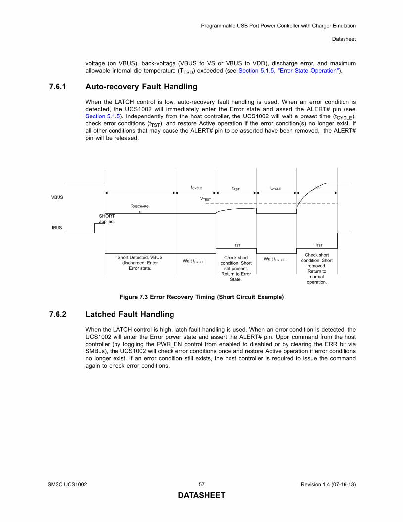
Programmable USB Port Power Controller with Charger Emulation
Datasheet
voltage (on VBUS), back-voltage (VBUS to VS or VBUS to VDD), discharge error, and maximumallowable internal die temperature (TTSD) exceeded (see Section 5.1.5, "Error State Operation").
7.6.1 Auto-recovery Fault Handling
When the LATCH control is low, auto-recovery fault handling is used. When an error condition isdetected, the UCS1002 will immediately enter the Error state and assert the ALERT# pin (seeSection 5.1.5). Independently from the host controller, the UCS1002 will wait a preset time (tCYCLE),check error conditions (tTST), and restore Active operation if the error condition(s) no longer exist. Ifall other conditions that may cause the ALERT# pin to be asserted have been removed, the ALERT#pin will be released.
7.6.2 Latched Fault Handling
When the LATCH control is high, latch fault handling is used. When an error condition is detected, theUCS1002 will enter the Error power state and assert the ALERT# pin. Upon command from the hostcontroller (by toggling the PWR_EN control from enabled to disabled or by clearing the ERR bit viaSMBus), the UCS1002 will check error conditions once and restore Active operation if error conditionsno longer exist. If an error condition still exists, the host controller is required to issue the commandagain to check error conditions.
Figure 7.3 Error Recovery Timing (Short Circuit Example)
tRST
VBUS
IBUS
SHORT applied.
ITST
tDISCHARG
E
ITST
VTEST
Short Detected. VBUS discharged. Enter
Error state.
Check short condition. Short
still present. Return to Error
State.
Wait tCYCLE. Wait tCYCLE.Check short
condition. Short removed. Return to normal
operation.
tCYCLE tCYCLEtRST
SMSC UCS1002 57 Revision 1.4 (07-16-13)
DATASHEET
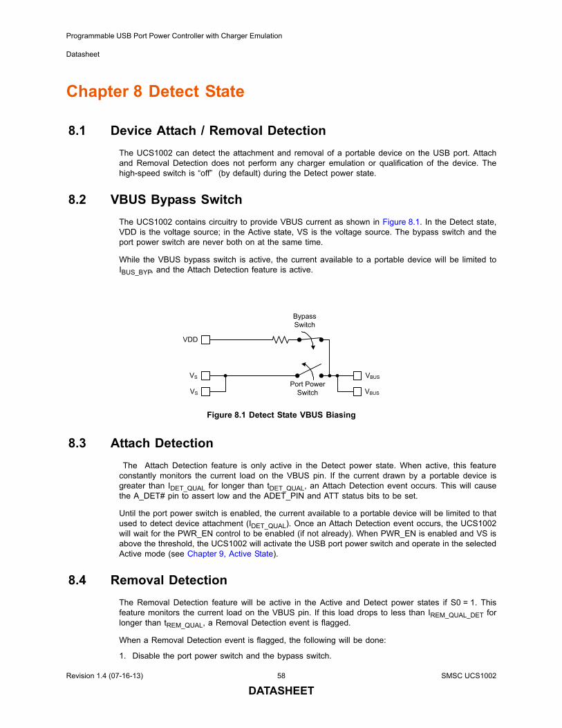
Programmable USB Port Power Controller with Charger Emulation
Datasheet
Chapter 8 Detect State
8.1 Device Attach / Removal Detection
The UCS1002 can detect the attachment and removal of a portable device on the USB port. Attachand Removal Detection does not perform any charger emulation or qualification of the device. Thehigh-speed switch is “off” (by default) during the Detect power state.
8.2 VBUS Bypass Switch
The UCS1002 contains circuitry to provide VBUS current as shown in Figure 8.1. In the Detect state,VDD is the voltage source; in the Active state, VS is the voltage source. The bypass switch and theport power switch are never both on at the same time.
While the VBUS bypass switch is active, the current available to a portable device will be limited toIBUS_BYP, and the Attach Detection feature is active.
8.3 Attach Detection
The Attach Detection feature is only active in the Detect power state. When active, this featureconstantly monitors the current load on the VBUS pin. If the current drawn by a portable device isgreater than IDET_QUAL for longer than tDET_QUAL, an Attach Detection event occurs. This will causethe A_DET# pin to assert low and the ADET_PIN and ATT status bits to be set.
Until the port power switch is enabled, the current available to a portable device will be limited to thatused to detect device attachment (IDET_QUAL). Once an Attach Detection event occurs, the UCS1002will wait for the PWR_EN control to be enabled (if not already). When PWR_EN is enabled and VS isabove the threshold, the UCS1002 will activate the USB port power switch and operate in the selectedActive mode (see Chapter 9, Active State).
8.4 Removal Detection
The Removal Detection feature will be active in the Active and Detect power states if S0 = 1. Thisfeature monitors the current load on the VBUS pin. If this load drops to less than IREM_QUAL_DET forlonger than tREM_QUAL, a Removal Detection event is flagged.
When a Removal Detection event is flagged, the following will be done:
1. Disable the port power switch and the bypass switch.
Figure 8.1 Detect State VBUS Biasing
Port Power Switch
VDD
VS
VS
VBUS
VBUS
Bypass Switch
Revision 1.4 (07-16-13) 58 SMSC UCS1002
DATASHEET
Programmable USB Port Power Controller with Charger Emulation
Datasheet
2. De-assert the A_DET# pinUCS1002 and set the REM status register bit.
3. Enable an internal discharging device that will discharge the VBUS line within tDISCHARGE.
4. Once the VBUS pin has been discharged, the device will return to the Detect state regardless ofthe PWR_EN control state.
SMSC UCS1002 59 Revision 1.4 (07-16-13)
DATASHEET
Programmable USB Port Power Controller with Charger Emulation
Datasheet
Chapter 9 Active State
9.1 Active State Overview
The UCS1002 has the following modes of operation in the Active state: Data Pass-through, BC1.2DCP, BC1.2 SDP, BC1.2 CDP, and Dedicated Charger Emulation Cycle. The current limiting modedepends on the Active mode behavior (see Table 9.2, "Current Limit Mode Options").
9.2 Active Mode Selection
The Active mode selection is controlled by three controls: EM_EN, M1, and M2, as shown in Table 9.1.
Note 9.1 BC1.2 SDP behaves the same as the Data Pass-through mode with the exception that itis preceded by a VBUS discharge when the mode is entered per the BC1.2 specification.
9.3 BC1.2 Detection Renegotiation
The BC1.2 specification allows a charger to act as an SDP, CDP, or DCP and to change between theseroles. To force an attached portable device to repeat the charging detection procedure, VBUS must becycled. In compliance with this specification, the UCS1002 automatically cycles VBUS when switchingbetween the BC1.2 SDP, BC1.2 DCP, and BC1.2 CDP modes.
9.4 Data Pass-through (No Charger Emulation)
When commanded to Data Pass-through mode, UCS1002 will close its USB high-speed data switchto allow USB communications between a portable device and host controller and will operate using tripcurrent limiting. No charger emulation profiles are applied in this mode. Data Pass-through mode willpersist until commanded otherwise by the M1, M2, and EM_EN controls.
APPLICATION NOTE: If it is desired that the Data Pass-through mode operates as a traditional / standard portpower switch, the S0 control should be set to ‘0’. When entering this mode, there is noautomatic VBUS discharge.
Table 9.1 Active Mode Selection
# M1 M2 EM_EN ACTIVE MODE
1 0 0 1 Dedicated Charger Emulation Cycle
2 0 1 0 Data Pass-through
3 0 1 1 BC1.2 DCP
4 1 0 0 BC1.2 SDP - See Note 9.1
5 1 0 1 Dedicated Charger Emulation Cycle
6 1 1 0 Data Pass-through
7 1 1 1 BC1.2 CDP
Revision 1.4 (07-16-13) 60 SMSC UCS1002
DATASHEET
Programmable USB Port Power Controller with Charger Emulation
Datasheet
APPLICATION NOTE: When the M1, M2, and EM_EN controls are set to ‘0’, ‘1’, ‘0’ or to ‘1’, ‘1’, ‘0’ respectively,Data Pass-through mode will persist if the PWR_EN control is disabled; however, theUCS1002 will draw more current. To leave Data Pass-through mode, the PWR_EN controlmust be enabled before the M1, M2, and EM_EN controls are changed to the desired mode.
9.5 BC1.2 SDP (No Charger Emulation)
When commanded to BC1.2 SDP mode, UCS1002 will discharge VBUS, close its USB high-speeddata switch to allow USB communications between a portable device and host controller, and willoperate using trip current limiting. No charger emulation profiles are applied in this mode. BC1.2 SDPmode will persist until commanded otherwise by the M1, M2, EM_EN, and PWR_EN controls.
APPLICATION NOTE: If it is desired that the BC1.2 SDP mode operates as a traditional / standard port powerswitch, the S0 control should be set to ‘0’.
9.6 BC1.2 CDP
When BC1.2 CDP is selected as the Active mode, UCS1002 will discharge VBUS, close its USB high-speed data switch (by default), and apply the BC1.2 CDP charger emulation profile which performshandshaking per the specification. The combination of the UCS1002 CDP handshake along with astandard USB host comprises a charging downstream port. In BC1.2 CDP mode, there is no emulationtimeout.
If the handshake is successful, the UCS1002 will operate using constant current limiting (variableslope). If the handshake is not successful, the UCS1002 will leave the applied CDP profile in place,leave the high-speed switch closed, enable constant current limiting, and persist in this condition untilcommanded otherwise by the M1, M2, EM_EN, and PWR_EN controls.
The UCS1002 will respond per the BC1.2 specification to portable device initiated chargerrenegotiation requests.
APPLICATION NOTE: BC1.2 compliance testing may require the S0 control to be set to ‘0’ (Attach and RemovalDetection feature disabled) while testing is in progress.
APPLICATION NOTE: When the UCS1002 is in BC1.2 CDP mode and the Attach and Removal Detection featureis enabled, if a power thief, such as a USB light or fan, attaches but does not assert DP, aRemoval event will not occur when the portable device is removed. However, if a standardUSB device is subsequently attached, Removal Detection will again be fully functional. Aswell, if PWR_EN is cycled or M1, M2, and / or EM_EN change state, a Removal event willoccur and Attach Detection will be reactivated.
9.6.1 BC1.2 CDP Charger Emulation Profile
The BC1.2 CDP charger emulation profile acts as described below.
APPLICATION NOTE: All CDP handshaking is performed with the high-speed switch closed.
1. VBUS voltage is applied.
2. Primary Detection - When the portable device drives a voltage between 0.4 V and 0.8 V onto theDPOUT pin, the UCS1002 will drive 0.6 V onto the DMOUT pin within 20 ms.
3. When the portable device drives the DPOUT pin back to ‘0’, the UCS1002 will then drive theDMOUT pin back to ‘0’ within 20 ms.
SMSC UCS1002 61 Revision 1.4 (07-16-13)
DATASHEET
Programmable USB Port Power Controller with Charger Emulation
Datasheet
4. Optional Secondary Detection - If the portable device then drives a voltage of 0.6 V (nominal) ontothe DMOUT pin, the UCS1002 will take no other action. This will cause the portable device toobserve a ‘0’ on the DPOUT pin and know that it is connected to a CDP.
9.7 BC1.2 DCP
When BC1.2 DCP is selected as the Active mode, UCS1002 will discharge VBUS and apply the BC1.2DCP charger emulation profile per the specification. In BC1.2 DCP mode, the emulation timeout andrequirement for portable device current draw are automatically disabled. When the BC1.2 DCP chargeremulation profile is applied within the Dedicated Charger Emulation Cycle (see Section 9.11.1, "BC1.2DCP Charger Emulation Profile Within DCE Cycle"), the timeout and current draw requirement areenabled.
If the portable device is charging after the DCP charger emulation profile is applied, the UCS1002 willleave in place the resistive short, leave the high-speed switch open, and enable constant currentlimiting (variable slope).
APPLICATION NOTE: BC1.2 compliance testing may require the S0 control to be set to ‘0’ (Attach and RemovalDetection feature disabled) while testing is in progress.
9.7.1 BC1.2 DCP Charger Emulation Profile
The BC1.2 DCP charger emulation profile is described below.
1. VBUS voltage is applied. A resistor (RDCP_RES) is connected between the DPOUT and DMOUTpins.
2. Primary Detection - If the portable device drives 0.6 V (nominal) onto the DPOUT pin, the UCS1002will take no other action than to leave the resistor connected between DPOUT and DMOUT. Thiswill cause the portable device to see 0.6 V (nominal) on the DMOUT pin and know that it isconnected to a DCP.
3. Optional Secondary Detection - If the portable device drives 0.6 V (nominal) onto the DMOUT pin,the UCS1002 will take no other action than to leave the resistor connected between DPOUT andDMOUT. This will cause the portable device to see 0.6 V (nominal) on the DPOUT pin and knowthat it is connected to a DCP.
9.8 Dedicated Charger
When commanded to Dedicated Charger Emulation Cycle mode, the UCS1002 enables an attachedportable device to enter its charging mode by applying specific charger emulation profiles in apredefined sequence. Using these profiles, the UCS1002 is capable of generating and recognizingseveral signal levels on the DPOUT and DMOUT pins. The preloaded charger emulation profilesinclude ones compatible with BC1.2 DCP, YD/T-1591 (2009) and most Apple and RIM portabledevices. Other levels, sequences, and protocols are configurable via the SMBus / I2C.
When a charger emulation profile is applied, a programmable timer for the emulation profile is started.When emulation timeout occurs, the UCS1002 checks the IBUS current against a programmablethreshold. If the current is above the threshold, the charger emulation profile is accepted and theassociated current limiting mode is applied. No active USB data communication is possible whencharging in this mode (by default - see Section 10.4.5, "High-speed Switch Configuration - 25h").
9.8.1 Emulation Reset
Prior to applying any of the charger emulation profiles, the UCS1002 will perform an emulation reset.This involves the following:
Revision 1.4 (07-16-13) 62 SMSC UCS1002
DATASHEET
Programmable USB Port Power Controller with Charger Emulation
Datasheet
1. The UCS1002 resets the VBUS line by disconnecting the port power switch and connecting VBUSto ground via an internal 100 Ω resistor for tDISCHARGE time. The port power switch will be heldopen for a time equal to tEM_RESET at which point the port power switch will be closed and theVBUS voltage applied.
2. The DPOUT and DMOUT pins will be pulled low using internal 15 kΩ pull-down resistors.
APPLICATION NOTE: To help prevent possible damage to a portable device, the DPOUT and DMOUT pins havecurrent limiting in place when the emulation profiles are applied.
9.8.2 Emulation Cycling
In Dedicated Charger Emulation Cycle mode, the charger emulation profiles (if enabled) will be appliedin the following order:
1. Legacy 1
2. BC1.2 DCP
3. Legacy 2
4. Legacy 3
5. Legacy 4
6. Legacy 5
7. Legacy 6
8. Legacy 7
9. Custom (disabled by default). If the CS1_FIRST configuration bit is set, then the Custom chargeremulation profile will be tested first and the order will proceed as given.
APPLICATION NOTE: If S0=’0’ and a portable device is not attached in DCE Cycle mode, the UCS1002 will becycling through charger emulation profiles (by default). There is no guarantee which chargeremulation profile will be applied first when a portable device attaches.
The UCS1002 will apply a charger emulation profile until one of the following exit conditions occurs:
1. Current greater than IBUS_CHG is detected flowing out of VBUS at the respective emulation timeouttime. In this case, the profile is assumed to be accepted and no other profiles will be applied.
2. The respective emulation timeout (tEM_TIMEOUT) time is reached without current that exceeds theIBUS_CHG limit flowing out of VBUS (the emulation timeout is enabled by default, see Section10.4.2, "Emulation Configuration - 16h" and Section 10.13.1, "Custom Emulation Configuration -40h"). The profile is assumed to be rejected, and the UCS1002 will perform emulation reset andapply the next profile, if there is one.
Emulation timeouts can be programmed for each charger emulation profile (see Section 10.11,"Preloaded Emulation Timeout Configuration Registers" and Section 10.13.1, "Custom EmulationConfiguration - 40h").
9.8.3 DCE Cycle Retry
If none of the charger emulation profiles cause a charge current to be drawn, the UCS1002 will performemulation reset and cycle through the profiles again (if the EM_RETRY bit is set (default - see Section10.4.2, "Emulation Configuration - 16h")). The UCS1002 will continue to cycle through the profiles soas long as charging current is not drawn and the PWR_EN control is enabled. If the Emulation Retryis not enabled, the UCS1002 will flag “no handshake” and end the DCE Cycle using trip currentlimiting.
SMSC UCS1002 63 Revision 1.4 (07-16-13)
DATASHEET
Programmable USB Port Power Controller with Charger Emulation
Datasheet
9.9 Current Limit Mode Associations
The UCS1002 will close the port power switch and use the current limiting mode as shown in Table 9.2.
As noted in the last three rows in Table 9.2, under those specific conditions with ILIM < 1.5 A, it is therelationship of ILIM and IBUS_R2MIN that determines the current limiting mode. In these cases, the valueof IBUS_R2MIN is determined by CS_R2_IMIN[2:0] bits 4-2 in the Custom Current Limiting BehaviorConfiguration register 51h.
9.10 No Handshake
In DCE Cycle mode with emulation retry disabled, a “no handshake” condition is flagged (the NO_HSstatus bit stays set (see Section 10.3.4, "Profile Status 1 - 12h")) when the end of the DCE Cycle isreached without a handshake and without drawing current.
All signatures / handshaking placed on the DPOUT and DMOUT pins are removed. The UCS1002 willoperate with the high-speed switch opened or closed as determined by the high-speed switchconfiguration and will use trip or constant current limiting as determined by the IBUS_R2MIN setting(CS_R2_IMIN[2:0] bits 4-2 in the Custom Current Limiting Behavior Configuration register 51h).
Table 9.2 Current Limit Mode Options
ACTIVE MODECURRENT LIMIT MODE
(SEE Section 10.14)
Data Pass-through Trip mode
BC1.2 DCP CC mode if ILIM < 1.5 A, otherwise, trip mode
BC1.2 SDP Trip mode
BC1.2 CDP CC mode if ILIM < 1.5 A, otherwise, trip mode
DCE CYCLE
During DCE Cycle when a charger emulation profile is being applied and the emulation timeout is active
CC mode if ILIM < 1.5 A, otherwise, trip mode
BC1.2 DCP charger emulation profile accepted or the emulation timeout is disabled
CC mode if ILIM < 1.5 A, otherwise, trip mode
Legacy 2 charger emulation profile accepted or the emulation timeout is disabled
CC mode if ILIM < 1.5 A, otherwise, trip mode
Legacy 1 or Legacy 3 - Legacy 7 charger emulation profile accepted or the emulation timeout is disabled
Trip mode if IBUS_R2MIN < ILIM or ILIM > 1.5 A (normal operation), otherwise, CC mode (see Section 10.14.2)
Custom charger emulation profile accepted or the emulation timeout is disabled
Trip mode if IBUS_R2MIN < ILIM or ILIM > 1.5 A (normal operation), otherwise, CC mode (see Section 10.14.2)
No handshake (DCE Cycle with Emulation Retry not enabled)
Trip mode if IBUS_R2MIN < ILIM or ILIM > 1.5 A (normal operation), otherwise, CC mode (see Section 10.14.2)
Revision 1.4 (07-16-13) 64 SMSC UCS1002
DATASHEET
Programmable USB Port Power Controller with Charger Emulation
Datasheet
Portable devices that can cause this are generally ones that pull up DPOUT to some voltage and leaveit there, or apply the wrong voltage.
9.11 Preloaded Charger Emulation Profiles
The following charger emulation profiles are resident to the UCS1002:
1. Legacy 1, 3, 4, and 6 - See Section 9.11.3
2. Legacy 2 - See Section 9.11.2
3. Legacy 5 - See Section 9.11.4
4. Legacy 7 - See Section 9.11.5
5. BC1.2 CDP - See Section 9.6.1
6. BC1.2 DCP - See Section 9.7.1
Additionally, the user may “build” a charger emulation profile by determining the voltage and resistancecharacteristics that are placed on each of the DPOUT and DMOUT pins. See Section 9.12, "CustomCharger Emulation Profile".
9.11.1 BC1.2 DCP Charger Emulation Profile Within DCE Cycle
When the BC1.2 DCP charger emulation profile (Section 9.7.1, "BC1.2 DCP Charger EmulationProfile") is applied within the DCE Cycle (Dedicated Charger Emulation Cycle is selected as the Activemode), the behavior after the profile is applied is different than Active mode BC1.2 DCP (BC1.2 DCPin Table 9.1) because the tEM_TIMEOUT timer is enabled (by default) during the DCE Cycle.
During the DCE Cycle after the DCP charger emulation profile, the UCS1002 will perform one of thefollowing:
1. If the portable device is drawing more than IBUS_CHG current when the tEM_TIMEOUT timer expires,the UCS1002 will flag that a BC1.2 DCP was detected. The UCS1002 will leave in place theresistive short, leave the high-speed switch open, and then enable constant current limiting(variable slope).
2. If the portable device does not draw more than IBUS_CHG current when the tEM_TIMEOUT timerexpires, the UCS1002 will stop applying the DCP charger emulation profile and proceed to the nextcharger emulation profile in the DCE Cycle.
9.11.2 Legacy 2 Charger Emulation Profile
The Legacy 2 charger emulation profile does the following:
1. The UCS1002 will connect a resistor (RDCP_RES) between DPOUT and DMOUT.
2. VBUS is applied.
3. If the portable device draws more than IBUS_CHG current when the tEM_TIMEOUT timer expires(enabled by default), the UCS1002 will accept that this is the correct charger emulation profile forthe attached portable device. Charging commences. The resistive short between the DPOUT andDMOUT pins will be left in place. The UCS1002 will use constant current limiting.
4. If the portable device does not draw more than IBUS_CHG current when tEM_TIMEOUT timer expires,the UCS1002 will stop the Legacy 2 charger emulation. This will cause resistive short between theDPOUT and DMOUT pins to be removed. Emulation reset occurs, and the UCS1002 will initiatethe next charger emulation profile.
SMSC UCS1002 65 Revision 1.4 (07-16-13)
DATASHEET
Programmable USB Port Power Controller with Charger Emulation
Datasheet
9.11.3 Legacy 1, 3, 4, and 6 Charger Emulation Profiles
Legacy 1, 3, 4, and 6 charger emulation profiles follow the same pattern of operation although thevoltage that is applied on the DPOUT and DMOUT pins will vary. They do the following:
1. The UCS1002 will apply a voltage on the DPOUT pin using either a current-limited voltage sourceor a voltage divider between VBUS and ground with the center tap on the DPOUT pin.
2. The UCS1002 will apply a possibly different voltage on the DMOUT pin using either a current-limited voltage source or a voltage divider between VBUS and ground with the center tap on theDMOUT pin.
3. VBUS voltage is applied.
4. If the portable device draws more than IBUS_CHG current when the tEM_TIMEOUT timer expires, theUCS1002 will accept that the currently applied profile is the correct charger emulation profile forthe attached portable device. Charging commences. The voltages applied to the DPOUT andDMOUT pins will remain in place (unless LEAVE_EMU_RESP is set to 0b). The UCS1002 willbegin operating in trip mode or CC mode as determined by the IBUS_R2MIN setting (see Section10.14, "Current Limiting Behavior Configuration Registers").
5. If the portable device does not draw more than IBUS_CHG current when tEM_TIMEOUT timer expires,the UCS1002 will stop the currently applied charger emulation profile. This will cause all voltagesput onto the DPOUT and DMOUT pins to be removed. Emulation reset occurs, and the UCS1002will initiate the next charger emulation profile.
9.11.4 Legacy 5 Charger Emulation Profile
Legacy 5 charger emulation profile does the following:
1. The UCS1002 will apply 900 mV to both the DPOUT and the DMOUT pins.
2. VBUS voltage is applied.
3. If the portable device draws more than IBUS_CHG current when the tEM_TIMEOUT timer expires, theUCS1002 will accept that the currently applied profile is the correct charger emulation profile forthe attached portable device. Charging commences. The voltages applied to the DPOUT andDMOUT pins will remain in place (unless LEAVE_EMU_RESP is set to 0b). The UCS1002 willbegin operating in trip mode or CC mode as determined by the IBUS_R2MIN setting (see Section10.14, "Current Limiting Behavior Configuration Registers").
4. If the portable device does not draw more than IBUS_CHG current when tEM_TIMEOUT timer expires,the UCS1002 will stop the currently applied charger emulation profile. This will cause all voltagesput onto the DPOUT and DMOUT pins to be removed. Emulation reset occurs, and the UCS1002will initiate the next charger emulation profile.
9.11.5 Legacy 7 Charger Emulation Profile
The Legacy 7 charger emulation profile does the following:
1. The UCS1002 will apply a voltage on the DPOUT pin using a voltage divider between VBUS andground with the center tap on the DPOUT pin.
2. VBUS voltage is applied.
3. If the portable device draws more than IBUS_CHG current when the tEM_TIMEOUT timer expires, theUCS1002 will accept that Legacy 7 is the correct charger emulation profile for the attached portabledevice. Charging commences. The voltage applied to the DPOUT pin will remain in place (unlessLEAVE_EMU_RESP is set to 0b). The UCS1002 will begin operating in trip mode or CC mode asdetermined by the IBUS_R2MIN setting (see Section 10.14, "Current Limiting Behavior ConfigurationRegisters").
Revision 1.4 (07-16-13) 66 SMSC UCS1002
DATASHEET
Programmable USB Port Power Controller with Charger Emulation
Datasheet
4. If the portable device does not draw more than IBUS_CHG current when tEM_TIMEOUT timer expires,the UCS1002 will stop the Legacy 7 charger emulation profile. This will cause the voltage put ontothe DPOUT pin to be removed. Emulation reset occurs, and the UCS1002 will initiate the nextcharger emulation profile.
9.12 Custom Charger Emulation Profile
The UCS1002 allows the user to create a Custom charger emulation profile to handshake as any typeof charger. This profile can be included in the DCE Cycle. In addition, it can be placed first or last inthe profile sequence in the DCE Cycle. See Section 10.13.1, "Custom Emulation Configuration - 40h".
The Custom charger emulation profile uses a number of registers to define stimuli and behaviors. TheCustom charger emulation profile uses three separate stimulus / response pairs that will be detectedand applied in sequence, allowing flexibility to “build” any of the preloaded emulation profiles or tailorthe profile to match a specific charger application.
For details, see application note 24.14 “UCS1002 Fundamentals of Custom Charger Emulation.
SMSC UCS1002 67 Revision 1.4 (07-16-13)
DATASHEET
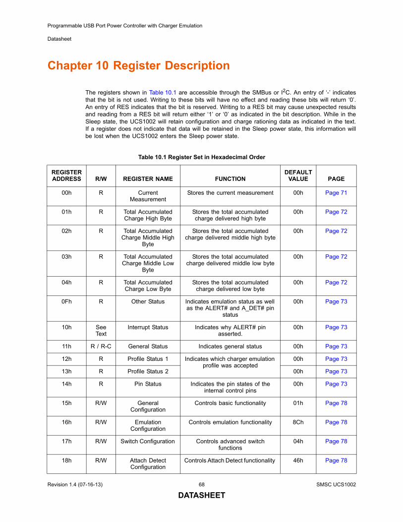
Programmable USB Port Power Controller with Charger Emulation
Datasheet
Chapter 10 Register Description
The registers shown in Table 10.1 are accessible through the SMBus or I2C. An entry of ‘-’ indicatesthat the bit is not used. Writing to these bits will have no effect and reading these bits will return ‘0’.An entry of RES indicates that the bit is reserved. Writing to a RES bit may cause unexpected resultsand reading from a RES bit will return either ‘1’ or ‘0’ as indicated in the bit description. While in theSleep state, the UCS1002 will retain configuration and charge rationing data as indicated in the text.If a register does not indicate that data will be retained in the Sleep power state, this information willbe lost when the UCS1002 enters the Sleep power state.
Table 10.1 Register Set in Hexadecimal Order
REGISTERADDRESS R/W REGISTER NAME FUNCTION
DEFAULT VALUE PAGE
00h R Current Measurement
Stores the current measurement 00h Page 71
01h R Total Accumulated Charge High Byte
Stores the total accumulated charge delivered high byte
00h Page 72
02h R Total Accumulated Charge Middle High
Byte
Stores the total accumulated charge delivered middle high byte
00h Page 72
03h R Total Accumulated Charge Middle Low
Byte
Stores the total accumulated charge delivered middle low byte
00h Page 72
04h R Total Accumulated Charge Low Byte
Stores the total accumulated charge delivered low byte
00h Page 72
0Fh R Other Status Indicates emulation status as well as the ALERT# and A_DET# pin
status
00h Page 73
10h See Text
Interrupt Status Indicates why ALERT# pin asserted.
00h Page 73
11h R / R-C General Status Indicates general status 00h Page 73
12h R Profile Status 1 Indicates which charger emulation profile was accepted
00h Page 73
13h R Profile Status 2 00h Page 73
14h R Pin Status Indicates the pin states of the internal control pins
00h Page 73
15h R/W General Configuration
Controls basic functionality 01h Page 78
16h R/W Emulation Configuration
Controls emulation functionality 8Ch Page 78
17h R/W Switch Configuration Controls advanced switch functions
04h Page 78
18h R/W Attach Detect Configuration
Controls Attach Detect functionality 46h Page 78
Revision 1.4 (07-16-13) 68 SMSC UCS1002
DATASHEET
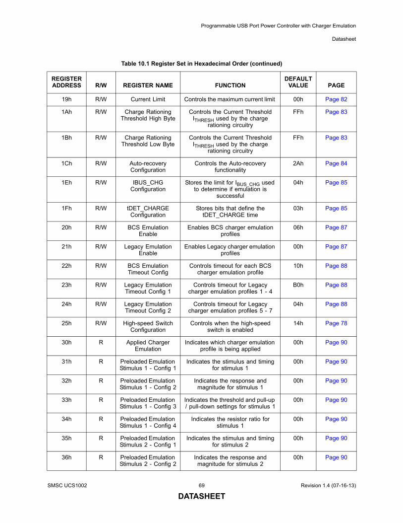
Programmable USB Port Power Controller with Charger Emulation
Datasheet
19h R/W Current Limit Controls the maximum current limit 00h Page 82
1Ah R/W Charge Rationing Threshold High Byte
Controls the Current Threshold ITHRESH used by the charge
rationing circuitry
FFh Page 83
1Bh R/W Charge Rationing Threshold Low Byte
Controls the Current Threshold ITHRESH used by the charge
rationing circuitry
FFh Page 83
1Ch R/W Auto-recovery Configuration
Controls the Auto-recovery functionality
2Ah Page 84
1Eh R/W IBUS_CHG Configuration
Stores the limit for IBUS_CHG used to determine if emulation is
successful
04h Page 85
1Fh R/W tDET_CHARGE Configuration
Stores bits that define the tDET_CHARGE time
03h Page 85
20h R/W BCS Emulation Enable
Enables BCS charger emulation profiles
06h Page 87
21h R/W Legacy Emulation Enable
Enables Legacy charger emulation profiles
00h Page 87
22h R/W BCS Emulation Timeout Config
Controls timeout for each BCS charger emulation profile
10h Page 88
23h R/W Legacy Emulation Timeout Config 1
Controls timeout for Legacy charger emulation profiles 1 - 4
B0h Page 88
24h R/W Legacy Emulation Timeout Config 2
Controls timeout for Legacy charger emulation profiles 5 - 7
04h Page 88
25h R/W High-speed Switch Configuration
Controls when the high-speed switch is enabled
14h Page 78
30h R Applied Charger Emulation
Indicates which charger emulation profile is being applied
00h Page 90
31h R Preloaded Emulation Stimulus 1 - Config 1
Indicates the stimulus and timing for stimulus 1
00h Page 90
32h R Preloaded Emulation Stimulus 1 - Config 2
Indicates the response and magnitude for stimulus 1
00h Page 90
33h R Preloaded Emulation Stimulus 1 - Config 3
Indicates the threshold and pull-up / pull-down settings for stimulus 1
00h Page 90
34h R Preloaded Emulation Stimulus 1 - Config 4
Indicates the resistor ratio for stimulus 1
00h Page 90
35h R Preloaded Emulation Stimulus 2 - Config 1
Indicates the stimulus and timing for stimulus 2
00h Page 90
36h R Preloaded Emulation Stimulus 2 - Config 2
Indicates the response and magnitude for stimulus 2
00h Page 90
Table 10.1 Register Set in Hexadecimal Order (continued)
REGISTERADDRESS R/W REGISTER NAME FUNCTION
DEFAULT VALUE PAGE
SMSC UCS1002 69 Revision 1.4 (07-16-13)
DATASHEET
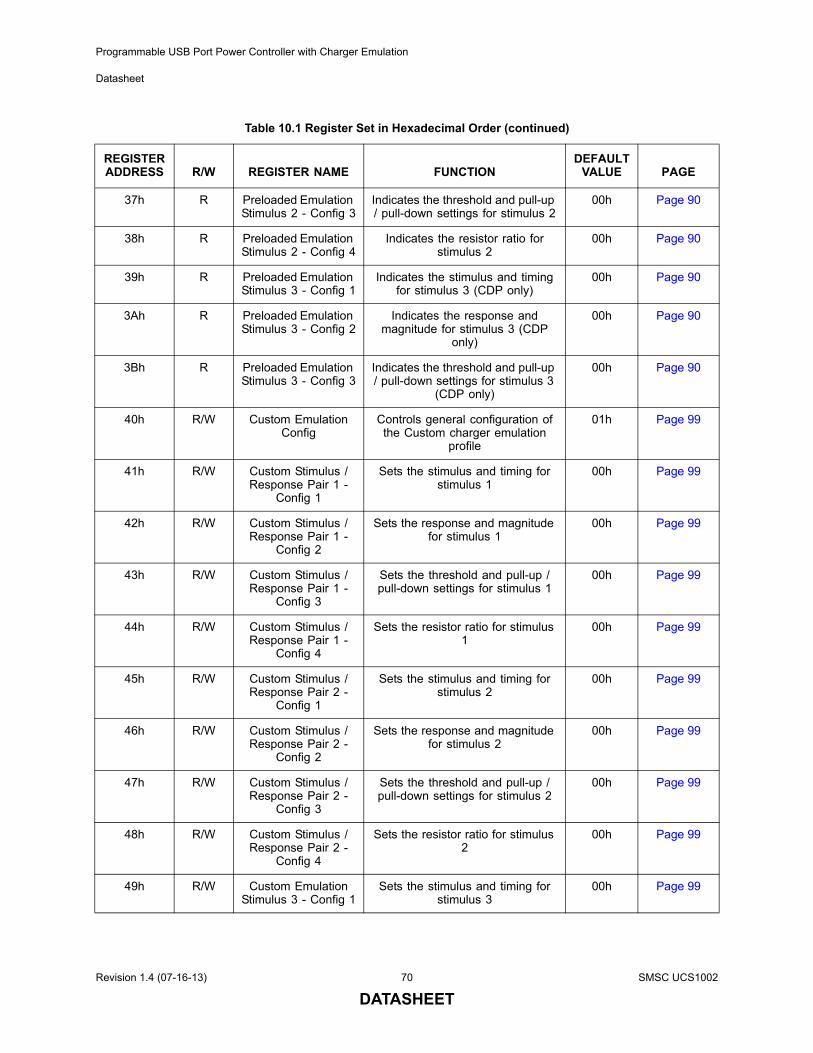
Programmable USB Port Power Controller with Charger Emulation
Datasheet
37h R Preloaded Emulation Stimulus 2 - Config 3
Indicates the threshold and pull-up / pull-down settings for stimulus 2
00h Page 90
38h R Preloaded Emulation Stimulus 2 - Config 4
Indicates the resistor ratio for stimulus 2
00h Page 90
39h R Preloaded Emulation Stimulus 3 - Config 1
Indicates the stimulus and timing for stimulus 3 (CDP only)
00h Page 90
3Ah R Preloaded Emulation Stimulus 3 - Config 2
Indicates the response and magnitude for stimulus 3 (CDP
only)
00h Page 90
3Bh R Preloaded Emulation Stimulus 3 - Config 3
Indicates the threshold and pull-up / pull-down settings for stimulus 3
(CDP only)
00h Page 90
40h R/W Custom Emulation Config
Controls general configuration of the Custom charger emulation
profile
01h Page 99
41h R/W Custom Stimulus / Response Pair 1 -
Config 1
Sets the stimulus and timing for stimulus 1
00h Page 99
42h R/W Custom Stimulus / Response Pair 1 -
Config 2
Sets the response and magnitude for stimulus 1
00h Page 99
43h R/W Custom Stimulus / Response Pair 1 -
Config 3
Sets the threshold and pull-up / pull-down settings for stimulus 1
00h Page 99
44h R/W Custom Stimulus / Response Pair 1 -
Config 4
Sets the resistor ratio for stimulus 1
00h Page 99
45h R/W Custom Stimulus / Response Pair 2 -
Config 1
Sets the stimulus and timing for stimulus 2
00h Page 99
46h R/W Custom Stimulus / Response Pair 2 -
Config 2
Sets the response and magnitude for stimulus 2
00h Page 99
47h R/W Custom Stimulus / Response Pair 2 -
Config 3
Sets the threshold and pull-up / pull-down settings for stimulus 2
00h Page 99
48h R/W Custom Stimulus / Response Pair 2 -
Config 4
Sets the resistor ratio for stimulus 2
00h Page 99
49h R/W Custom Emulation Stimulus 3 - Config 1
Sets the stimulus and timing for stimulus 3
00h Page 99
Table 10.1 Register Set in Hexadecimal Order (continued)
REGISTERADDRESS R/W REGISTER NAME FUNCTION
DEFAULT VALUE PAGE
Revision 1.4 (07-16-13) 70 SMSC UCS1002
DATASHEET
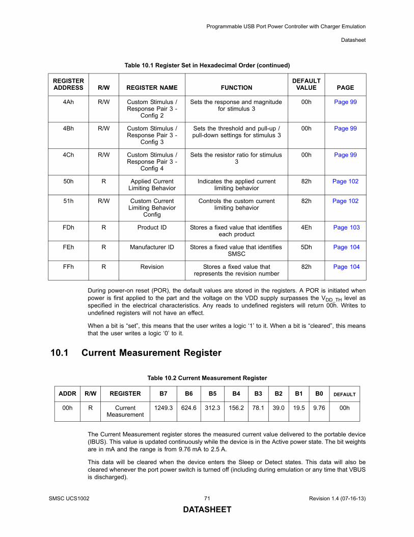
Programmable USB Port Power Controller with Charger Emulation
Datasheet
During power-on reset (POR), the default values are stored in the registers. A POR is initiated whenpower is first applied to the part and the voltage on the VDD supply surpasses the VDD_TH level asspecified in the electrical characteristics. Any reads to undefined registers will return 00h. Writes toundefined registers will not have an effect.
When a bit is “set”, this means that the user writes a logic ‘1’ to it. When a bit is “cleared”, this meansthat the user writes a logic ‘0’ to it.
10.1 Current Measurement Register
The Current Measurement register stores the measured current value delivered to the portable device(IBUS). This value is updated continuously while the device is in the Active power state. The bit weightsare in mA and the range is from 9.76 mA to 2.5 A.
This data will be cleared when the device enters the Sleep or Detect states. This data will also becleared whenever the port power switch is turned off (including during emulation or any time that VBUSis discharged).
4Ah R/W Custom Stimulus / Response Pair 3 -
Config 2
Sets the response and magnitude for stimulus 3
00h Page 99
4Bh R/W Custom Stimulus / Response Pair 3 -
Config 3
Sets the threshold and pull-up / pull-down settings for stimulus 3
00h Page 99
4Ch R/W Custom Stimulus / Response Pair 3 -
Config 4
Sets the resistor ratio for stimulus 3
00h Page 99
50h R Applied Current Limiting Behavior
Indicates the applied current limiting behavior
82h Page 102
51h R/W Custom Current Limiting Behavior
Config
Controls the custom current limiting behavior
82h Page 102
FDh R Product ID Stores a fixed value that identifies each product
4Eh Page 103
FEh R Manufacturer ID Stores a fixed value that identifies SMSC
5Dh Page 104
FFh R Revision Stores a fixed value that represents the revision number
82h Page 104
Table 10.2 Current Measurement Register
ADDR R/W REGISTER B7 B6 B5 B4 B3 B2 B1 B0 DEFAULT
00h R Current Measurement
1249.3 624.6 312.3 156.2 78.1 39.0 19.5 9.76 00h
Table 10.1 Register Set in Hexadecimal Order (continued)
REGISTERADDRESS R/W REGISTER NAME FUNCTION
DEFAULT VALUE PAGE
SMSC UCS1002 71 Revision 1.4 (07-16-13)
DATASHEET
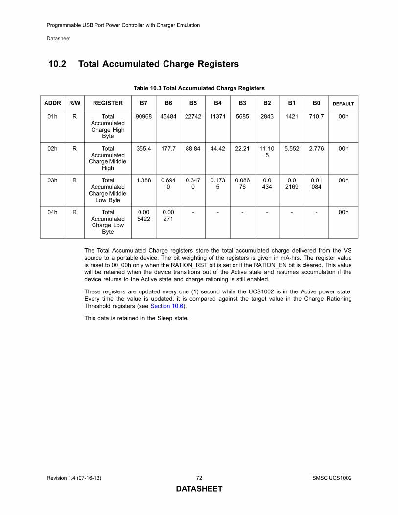
Programmable USB Port Power Controller with Charger Emulation
Datasheet
10.2 Total Accumulated Charge Registers
The Total Accumulated Charge registers store the total accumulated charge delivered from the VSsource to a portable device. The bit weighting of the registers is given in mA-hrs. The register valueis reset to 00_00h only when the RATION_RST bit is set or if the RATION_EN bit is cleared. This valuewill be retained when the device transitions out of the Active state and resumes accumulation if thedevice returns to the Active state and charge rationing is still enabled.
These registers are updated every one (1) second while the UCS1002 is in the Active power state.Every time the value is updated, it is compared against the target value in the Charge RationingThreshold registers (see Section 10.6).
This data is retained in the Sleep state.
Table 10.3 Total Accumulated Charge Registers
ADDR R/W REGISTER B7 B6 B5 B4 B3 B2 B1 B0 DEFAULT
01h R Total Accumulated Charge High
Byte
90968 45484 22742 11371 5685 2843 1421 710.7 00h
02h R Total Accumulated
Charge Middle High
355.4 177.7 88.84 44.42 22.21 11.105
5.552 2.776 00h
03h R Total Accumulated
Charge Middle Low Byte
1.388 0.6940
0.3470
0.1735
0.08676
0.0 434
0.0 2169
0.01 084
00h
04h R Total Accumulated Charge Low
Byte
0.00 5422
0.00 271
- - - - - - 00h
Revision 1.4 (07-16-13) 72 SMSC UCS1002
DATASHEET
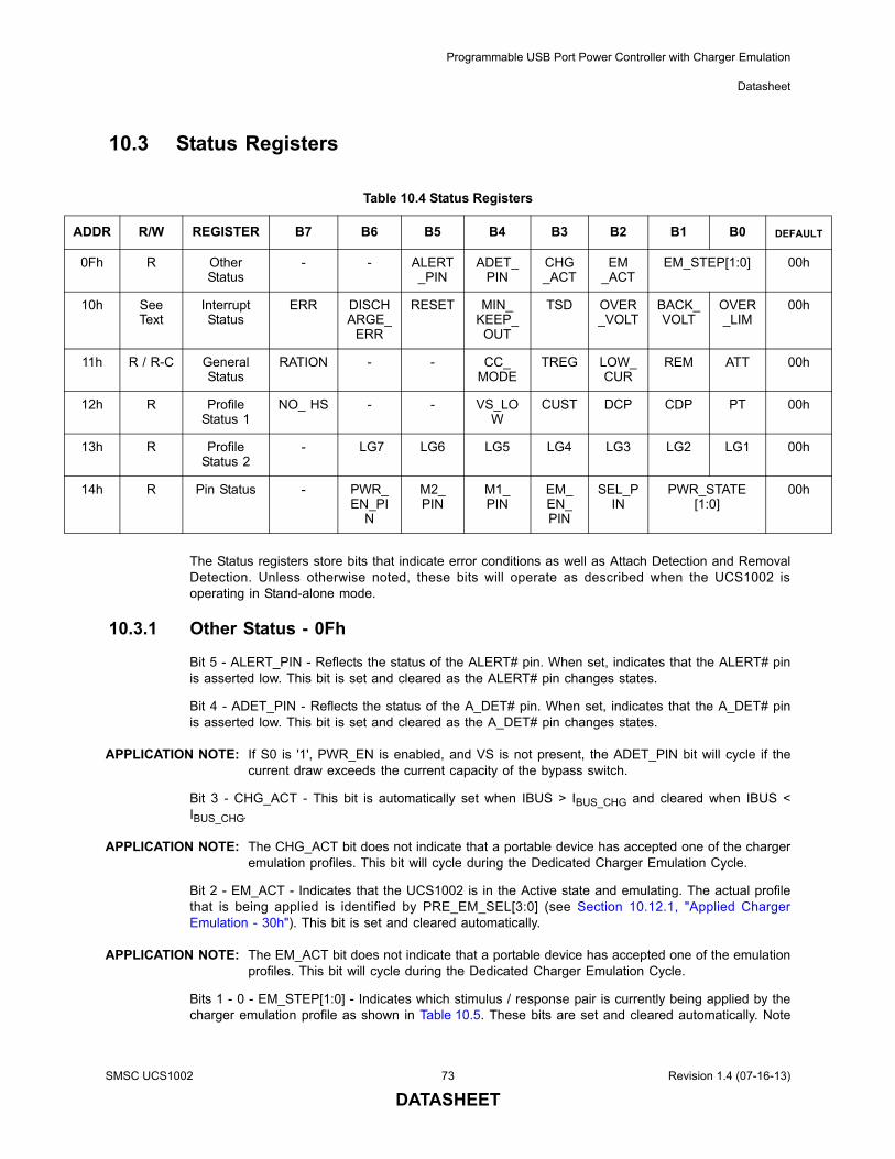
Programmable USB Port Power Controller with Charger Emulation
Datasheet
ADD LT
0F
10
11
12
13
14
10.3 Status Registers
The Status registers store bits that indicate error conditions as well as Attach Detection and RemovalDetection. Unless otherwise noted, these bits will operate as described when the UCS1002 isoperating in Stand-alone mode.
10.3.1 Other Status - 0Fh
Bit 5 - ALERT_PIN - Reflects the status of the ALERT# pin. When set, indicates that the ALERT# pinis asserted low. This bit is set and cleared as the ALERT# pin changes states.
Bit 4 - ADET_PIN - Reflects the status of the A_DET# pin. When set, indicates that the A_DET# pinis asserted low. This bit is set and cleared as the A_DET# pin changes states.
APPLICATION NOTE: If S0 is '1', PWR_EN is enabled, and VS is not present, the ADET_PIN bit will cycle if thecurrent draw exceeds the current capacity of the bypass switch.
Bit 3 - CHG_ACT - This bit is automatically set when IBUS > IBUS_CHG and cleared when IBUS <IBUS_CHG.
APPLICATION NOTE: The CHG_ACT bit does not indicate that a portable device has accepted one of the chargeremulation profiles. This bit will cycle during the Dedicated Charger Emulation Cycle.
Bit 2 - EM_ACT - Indicates that the UCS1002 is in the Active state and emulating. The actual profilethat is being applied is identified by PRE_EM_SEL[3:0] (see Section 10.12.1, "Applied ChargerEmulation - 30h"). This bit is set and cleared automatically.
APPLICATION NOTE: The EM_ACT bit does not indicate that a portable device has accepted one of the emulationprofiles. This bit will cycle during the Dedicated Charger Emulation Cycle.
Bits 1 - 0 - EM_STEP[1:0] - Indicates which stimulus / response pair is currently being applied by thecharger emulation profile as shown in Table 10.5. These bits are set and cleared automatically. Note
Table 10.4 Status Registers
R R/W REGISTER B7 B6 B5 B4 B3 B2 B1 B0 DEFAU
h R Other Status
- - ALERT_PIN
ADET_PIN
CHG _ACT
EM _ACT
EM_STEP[1:0] 00h
h See Text
Interrupt Status
ERR DISCHARGE_
ERR
RESET MIN_ KEEP_OUT
TSD OVER_VOLT
BACK_VOLT
OVER_LIM
00h
h R / R-C General Status
RATION - - CC_ MODE
TREG LOW_CUR
REM ATT 00h
h R Profile Status 1
NO_ HS - - VS_LOW
CUST DCP CDP PT 00h
h R Profile Status 2
- LG7 LG6 LG5 LG4 LG3 LG2 LG1 00h
h R Pin Status - PWR_EN_PI
N
M2_ PIN
M1_ PIN
EM_ EN_ PIN
SEL_PIN
PWR_STATE [1:0]
00h
SMSC UCS1002 73 Revision 1.4 (07-16-13)
DATASHEET
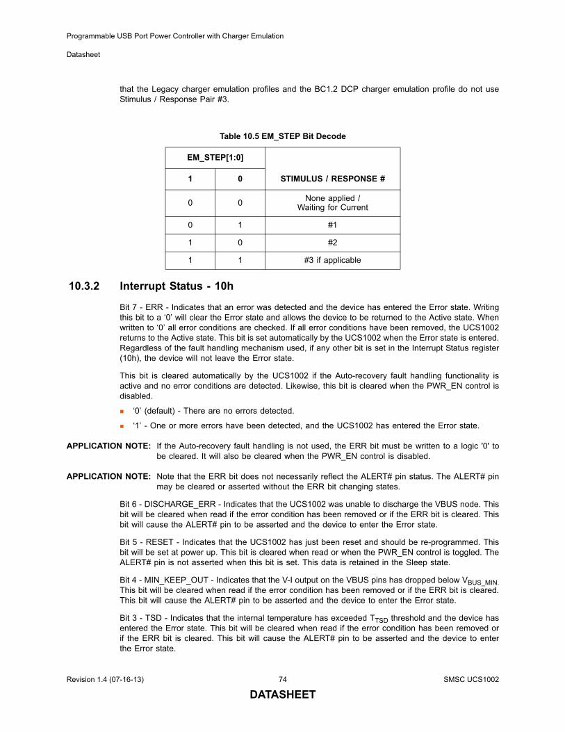
Programmable USB Port Power Controller with Charger Emulation
Datasheet
that the Legacy charger emulation profiles and the BC1.2 DCP charger emulation profile do not useStimulus / Response Pair #3.
10.3.2 Interrupt Status - 10h
Bit 7 - ERR - Indicates that an error was detected and the device has entered the Error state. Writingthis bit to a ‘0’ will clear the Error state and allows the device to be returned to the Active state. Whenwritten to ‘0’ all error conditions are checked. If all error conditions have been removed, the UCS1002returns to the Active state. This bit is set automatically by the UCS1002 when the Error state is entered.Regardless of the fault handling mechanism used, if any other bit is set in the Interrupt Status register(10h), the device will not leave the Error state.
This bit is cleared automatically by the UCS1002 if the Auto-recovery fault handling functionality isactive and no error conditions are detected. Likewise, this bit is cleared when the PWR_EN control isdisabled.
‘0’ (default) - There are no errors detected.
‘1’ - One or more errors have been detected, and the UCS1002 has entered the Error state.
APPLICATION NOTE: If the Auto-recovery fault handling is not used, the ERR bit must be written to a logic '0' tobe cleared. It will also be cleared when the PWR_EN control is disabled.
APPLICATION NOTE: Note that the ERR bit does not necessarily reflect the ALERT# pin status. The ALERT# pinmay be cleared or asserted without the ERR bit changing states.
Bit 6 - DISCHARGE_ERR - Indicates that the UCS1002 was unable to discharge the VBUS node. Thisbit will be cleared when read if the error condition has been removed or if the ERR bit is cleared. Thisbit will cause the ALERT# pin to be asserted and the device to enter the Error state.
Bit 5 - RESET - Indicates that the UCS1002 has just been reset and should be re-programmed. Thisbit will be set at power up. This bit is cleared when read or when the PWR_EN control is toggled. TheALERT# pin is not asserted when this bit is set. This data is retained in the Sleep state.
Bit 4 - MIN_KEEP_OUT - Indicates that the V-I output on the VBUS pins has dropped below VBUS_MIN.This bit will be cleared when read if the error condition has been removed or if the ERR bit is cleared.This bit will cause the ALERT# pin to be asserted and the device to enter the Error state.
Bit 3 - TSD - Indicates that the internal temperature has exceeded TTSD threshold and the device hasentered the Error state. This bit will be cleared when read if the error condition has been removed orif the ERR bit is cleared. This bit will cause the ALERT# pin to be asserted and the device to enterthe Error state.
Table 10.5 EM_STEP Bit Decode
EM_STEP[1:0]
STIMULUS / RESPONSE #1 0
0 0 None applied / Waiting for Current
0 1 #1
1 0 #2
1 1 #3 if applicable
Revision 1.4 (07-16-13) 74 SMSC UCS1002
DATASHEET
Programmable USB Port Power Controller with Charger Emulation
Datasheet
Bit 2 - OVER_VOLT - Indicates that the VS voltage has exceeded the VS_OV threshold and the devicehas entered the Error state. This bit will be cleared when read if the error condition has been removedor if the ERR bit is cleared. This bit will cause the ALERT# pin to be asserted and the device to enterthe Error state.
Bit 1 - BACK_VOLT - Indicates that the VBUS voltage has exceeded the VS or VDD voltages by morethan 150 mV. This bit will be cleared when read if the error condition has been removed or if the ERRbit is cleared. This bit will cause the ALERT# pin to be asserted and the device to enter the Error state.
Bit 0 - OVER_ILIM - Indicates that the IBUS current has exceeded both the ILIM threshold and theIBUS_R2MIN threshold settings. This bit will be cleared when read if the error condition has beenremoved or if the ERR bit is cleared. This bit will cause the ALERT# pin to be asserted and the deviceto enter the Error state.
10.3.3 General Status - 11h
Bit 7 - RATION - Indicates that the UCS1002 has delivered the programmed amount of power to aportable device. If the RATION_BEH bits are set to interrupt the host, this bit will cause the ALERT#pin to be asserted. This bit is cleared when read. This bit is also cleared automatically when theRATION_RST bit is set or the RATION_EN bit is cleared (see Section 10.4.1, "General Configuration- 15h").
Bit 4 - CC_MODE - Indicates that the IBUS current has exceeded ILIM.
Bit 3 - TREG - Indicates that the internal temperature has exceeded TREG and that the current limithas been reduced. This bit is cleared when read and will not cause the ALERT# pin to be assertedunless the ALERT_LINK bit is set.
Bit 2 - LOW_CUR - Indicates that a portable device has reduced its charge current to below ~6.4 mAand may be finished charging. This bit is cleared when read and will not cause the ALERT# pin to beasserted unless the ALERT_LINK bit is set.
Bit 1 - REM - Indicates that a Removal Detection event has occurred and there is no longer a portabledevice present. This bit is cleared when read and will not cause the ALERT# pin to be asserted. It willcause the A_DET# pin to be released.
Bit 0 - ATT - Indicates that an Attach Detection event has occurred and there is a new portable devicepresent. This bit is cleared when read and will not cause the ALERT# pin to be asserted. It will causethe A_DET# pin to be asserted.
10.3.4 Profile Status 1 - 12h
These bits are indicators only and will not cause the ALERT# pin or A_DET# pin to change states.The CUST, DCP, CDP, and PT bits are cleared under the following circumstances: the PWR_ENcontrol is disabled, a new Active mode is selected, or a Removal Detection event occurs.
Bit 7 - NO_HS - The NO_HS bit is only set during the Dedicated Charger Emulation Cycle (see Section9.10, "No Handshake"). This bit is automatically cleared whenever a new charger emulation profile isapplied.
APPLICATION NOTE: The NO_HS bit does not indicate that a portable device is drawing current and it may becleared to ‘0’ (indicating a handshake) and a portable device not charge. This bit is set atthe end of each charger emulation profile if a portable device does not handshake with it.This bit will not be set at the same time that any other Profile Status register bits are set.
Bit 4 - VS_LOW - Indicates that the VS voltage is below the VS_UVLO threshold and the port powerswitch is held off. This bit is cleared automatically when the VS voltage is above the VS_UVLO threshold.
SMSC UCS1002 75 Revision 1.4 (07-16-13)
DATASHEET
Programmable USB Port Power Controller with Charger Emulation
Datasheet
Bit 3 - CUST - Indicates that the portable device successfully performed a handshake with the user-defined Custom charger emulation profile during the DCE Cycle and is charging. Based on the Customcharger emulation profile configuration, the high-speed switch will be either open or closed (seeSection 10.13, "Custom Emulation Configuration Registers"). The port power switch current limitingmode is determined by the Custom current limiting behavior settings (see Section 10.14.2, "CustomCurrent Limiting Behavior Configuration - 51h").
Bit 2 - DCP - Indicates that the portable device accepted the BC1.2 DCP charger emulation profile andis charging. The high-speed switch will be controlled via the HSW_DCE bit (see Section 10.4.5, "High-speed Switch Configuration - 25h"), and the port power switch will use constant current limiting.
Bit 1 - CDP - Indicates that the portable device successfully performed a handshake with the BC1.2CDP charger emulation profile and is charging. The high-speed switch will be closed, and the portpower switch will use trip current limiting.
Bit 0 - PT - Indicates that the UCS1002 is in the Data Pass-through or BC1.2 SDP Active mode. Thehigh-speed switch will be closed, and the port power switch will use trip current limiting.
APPLICATION NOTE: When the UCS1002 is configured as a Data Pass-through and a Removal event and thenan Attach event occur without changing the Active mode, the PT bit will not be set againeven though the UCS1002 is still operating as a Data Pass-through as configured. Togglingthe M1 control will re-enable the PT status bit.
10.3.5 Profile Status 2 - 13h
These bits indicate which profile was accepted. These bits are indicators only and will not cause theALERT# pin or A_DET# pin to change states. These bits are cleared under the followingcircumstances: the PWR_EN control is disabled, a new Active mode is selected, or a RemovalDetection event occurs.
Bit 6 - LG7 - Indicates that the portable device successfully performed a handshake with the Legacy7 charger emulation profile and is charging. The high-speed switch will be controlled via the HSW_DCEbit (see Section 10.4.5, "High-speed Switch Configuration - 25h". The port power switch current limitingmode is determined by the Custom current limiting behavior settings (see Section 10.14.2, "CustomCurrent Limiting Behavior Configuration - 51h").
Bit 5 - LG6 - Indicates that the portable device successfully performed a handshake with the Legacy6 charger emulation profile and is charging. The high-speed switch will be controlled via the HSW_DCEbit (see Section 10.4.5, "High-speed Switch Configuration - 25h"). The port power switch currentlimiting mode is determined by the Custom current limiting behavior settings (see Section 10.14.2,"Custom Current Limiting Behavior Configuration - 51h").
Bit 4 - LG5 - Indicates that the portable device successfully performed a handshake with the Legacy5 charger emulation profile and is charging. The high-speed switch will be controlled via the HSW_DCEbit (see Section 10.4.5, "High-speed Switch Configuration - 25h"). The port power switch currentlimiting mode is determined by the Custom current limiting behavior settings (see Section 10.14.2,"Custom Current Limiting Behavior Configuration - 51h").
Bit 3 - LG4 - Indicates that the portable device successfully performed a handshake with the Legacy4 charger emulation profile and is charging. The high-speed switch will be controlled via the HSW_DCEbit (see Section 10.4.5, "High-speed Switch Configuration - 25h"). The port power switch currentlimiting mode is determined by the Custom current limiting behavior settings (see Section 10.14.2,"Custom Current Limiting Behavior Configuration - 51h").
Bit 2 - LG3 - Indicates that the portable device successfully performed a handshake with the Legacy3 charger emulation profile and is charging. The high-speed switch will be controlled via the HSW_DCEbit (see Section 10.4.5, "High-speed Switch Configuration - 25h"). The port power switch currentlimiting mode is determined by the Custom current limiting behavior settings (see Section 10.14.2,"Custom Current Limiting Behavior Configuration - 51h").
Revision 1.4 (07-16-13) 76 SMSC UCS1002
DATASHEET
Programmable USB Port Power Controller with Charger Emulation
Datasheet
Bit 1 - LG2 - Indicates that the portable device successfully performed a handshake with the Legacy2 charger emulation profile and is charging. The high-speed switch will be controlled via the HSW_DCEbit (see Section 10.4.5, "High-speed Switch Configuration - 25h"). The port power switch currentlimiting mode is determined by the Custom current limiting behavior settings (see Section 10.14.2,"Custom Current Limiting Behavior Configuration - 51h").
Bit 0 - LG1 - Indicates that the portable device successfully performed a handshake with the Legacy1 charger emulation profile and is charging. The high-speed switch will be controlled via the HSW_DCEbit (see Section 10.4.5, "High-speed Switch Configuration - 25h"). The port power switch currentlimiting mode is determined by the Custom current limiting behavior settings (see Section 10.14.2,"Custom Current Limiting Behavior Configuration - 51h").
10.3.6 Pin Status Register - 14h
The Pin Status register reflects the current pin state of the external control pins as well as identifyingthe power state. These bits are linked to the X_SET bits (see Section 10.4.3).
Bit 6 - PWR_EN_PIN - Reflects the PWR_EN control state. This bit is set and cleared automaticallyas the PWR_EN pin / PWR_EN_SET bit state changes.
Bit 5 - M2_PIN - Reflects the M2 pin state. This bit is set and cleared automatically as the M2 pin /M2_SET state changes.
Bit 4 - M1_PIN - Reflects the M1 pin state. This bit is set and cleared automatically as the M1 pin /M1_SET state changes.
Bit 3 - EM_EN_PIN - Reflects the EM_EN pin state. This bit is set and cleared automatically as theEM_EN pin / EM_EN_SET state changes.
Bit 2 - SEL_PIN - Reflects the polarity settings determined by the SEL pin decode. This bit is set orcleared automatically upon device power-up as the SEL pin is decoded.
‘0’ - The PWR_EN control is active low.
‘1’ - The PWR_EN control is active high.
Bits 1 - 0 - PWR_STATE[1:0] - Indicates the current power state as shown in Table 10.6. These bitsare set and cleared automatically as the power state changes.
APPLICATION NOTE: Accessing the SMBus / I2C causes the UCS1002 to leave the Sleep state. As a result, thePWR_STATE[1:0] bits will never read as 00b.
Table 10.6 PWR_STATE Bit Decode
PWR_STATE[1:0]
POWER STATE1 0
0 0 Sleep
0 1 Detect
1 0 Active
1 1 Error
SMSC UCS1002 77 Revision 1.4 (07-16-13)
DATASHEET
Programmable USB Port Power Controller with Charger Emulation
Datasheet
ADD ULT
15h h
16h h
17h h
18h h
25h h
10.4 Configuration Registers
The Configuration registers control basic device functionality.
10.4.1 General Configuration - 15h
The contents of this register are retained in Sleep.
Bit 7 - ALERT_MASK - Disables the ALERT# pin from asserting in the case of an error.
‘0’ (default) - The ALERT# pin will be asserted if an error condition or indicator event is detected.
‘1’ - The ALERT# pin will not be asserted in the event of an error condition.
Bit 5 - ALERT_LINK - Links the ALERT# pin to be asserted when the LOW_CUR and/or TREG bitsare set.
‘0’ (default) - The ALERT# pin will not be asserted if the LOW_CUR or TREG indicator bit is set.
‘1’ - The ALERT# pin will be asserted if the LOW_CUR or TREG indicator bit is set.
Bit 4 - DISCHARGE - Forces the VBUS to be reset and discharged when the UCS1002 is in the Activestate. Writing this bit to a logic ‘1’ will cause the port power switch to be opened and the dischargecircuitry to activate to discharge VBUS. The port power switch will remain open while this bit is ‘1’.This bit is not self-clearing.
Bit 3 - RATION_EN - Enables charge rationing functionality and power monitoring.
‘0’ (default) - Charge rationing is disabled. The Total Accumulated Charge registers will be cleared to 00_00h and current data will no longer be accumulated. If the Total Accumulated Charge registers have already reached the Charge Rationing Threshold (see Section 10.6, "Charge Rationing Threshold Registers"), the applied response will be removed as if the charge rationing had been reset. This will also clear the RATION status bit (if set).
‘1’ - Charge rationing is enabled (see Section 7.5, "Battery Full").
Bit 2 - RATION_RST - Resets the charge rationing functionality. When this bit is set to ‘1’, the TotalAccumulated Charge registers are reset to 00_00h. In addition, when this bit is set, the RATION statusbit will be cleared and, if there are no other errors or active indicators, the ALERT# pin will be released.
Table 10.7 Configuration Registers
R R/W REGISTER B7 B6 B5 B4 B3 B2 B1 B0 DEFA
R/W General Configuration
ALERT_ MASK
- ALERT_LINK
DISCHARGE
RATION_EN
RATION_RST
RATION_BEH [1:0]
01
R/W Emulation Configuration
DIS_TO - - EM_TIMEOUT_DIS
EM_R ETRY
LEAVE_EMU
_RESP
EM_RESET_ TIME[1:0]
8C
R/W Switch Configuration
PIN_IGNORE
- EM_ EN_ SET
M2_ SET
M1_ SET
S0_ SET
PWR_EN_ SET
LATCH_SET
04
R/W Attach Detect Configuration
0 1 0 0 DISCHG_TIME_ SEL[1:0]
ATT_TH[1:0] 46
R/W High-speed Switch
Configuration
- - - 1 HSW_CUST
HSW_ CDP
HSW_ DET
HSW_ DCE
14
Revision 1.4 (07-16-13) 78 SMSC UCS1002
DATASHEET
Programmable USB Port Power Controller with Charger Emulation
Datasheet
Bits 1 - 0 - RATION_BEH[1:0] - Controls the behavior when the power rationing threshold is reachedas shown in Table 7.1.
10.4.2 Emulation Configuration - 16h
The contents of this register are retained in Sleep.
Bit 7 - DIS_TO - Disables the timeout and idle reset functionality (see Section 4.2.1.6, "SMBus Timeoutand Idle Reset").
‘0’ - The timeout and idle reset functionality is enabled.
‘1’ (default) - The timeout and idle reset functionality is disabled. This is used for I2C compliance.
Bit 4 - EM_TIMEOUT_DIS - Disables the emulation circuitry timeout for all charger emulation profilesin the DCE Cycle. There is a separate bit to enable / disable the emulation timeout for the Customcharger emulation profile (Section 10.13.1, "Custom Emulation Configuration - 40h"); however, if theEM_TIMEOUT_DIS bit is set, the emulation timeout will also be disabled for the Custom chargeremulation profile.
APPLICATION NOTE: If the EM_TIMEOUT_DIS bit is set and the Legacy 1, Legacy 3, or Custom chargeremulation profiles were accepted during the DCE cycle, a removal is not detected. To avoidthis issue, re-enable the emulation timeout after applying any test profiles and charging withthe 'final' profile.
‘0’ (default) - Emulation timeout is enabled during the Dedicated Charger Emulation Cycle. An individual charger emulation profile will be applied and maintained for the duration of the tEM_TIMEOUT value. When this timer expires, the UCS1002 will determine whether the charger emulation profile was successful and take appropriate action.
‘1’ - Emulation timeout is disabled during the DCE Cycle. The applied charger emulation profile will not exit as a result of an emulation timeout event. The IBUS current will be checked continuously and if it exceeds the IBUS_CHG threshold for any reason, the charger emulation profile will be accepted.
Bit 3 - EM_RETRY - Configures whether the DCE Cycle will reset and restart if it reaches the finalprofile without the portable device drawing charging current and accepting one of the profiles. This bitis only used if the UCS1002 is configured to emulate a dedicated charger.
‘0’ - Once the DCE Cycle is completed, it will not restart. The DPOUT and DMOUT will be left as High-Z pins and the port power switch will be closed. The current limiting mode is determined by the Custom current limiting behavior settings (see Section 10.14.2, "Custom Current Limiting Behavior Configuration - 51h").
‘1’ (default) - Once the DCE Cycle is completed, it will perform emulation reset and restart from the first enabled charger emulation profile in the DCE Cycle.
Bit 2 - LEAVE_EMU_RESP - Enables the Dedicated Charger Emulation Cycle mode to hold theDPOUT and DMOUT stimulus response after the UCS1002 has finished emulation using the Legacy,BC1.2 DCP, or Custom charger emulation profiles.
APPLICATION NOTE: If the HSW_DCE bit is set, the high-speed switch will be closed regardless of the status ofthe LEAVE_EMU_RESP bit. Leaving the emulation response applied will not allow normalUSB traffic. Therefore, prior to setting the HSW_DCE bit, this bit should be cleared.
‘0’ - The dedicated emulation circuitry will behave normally. It will remove the short condition when the tEM_TIMEOUT timer has expired regardless if the portable device has drawn charging current or not.
‘1’ (default) - If a portable device begins drawing charging current while the UCS1002 is applying the BC1.2 DCP, Custom, or any of the Legacy charger emulation profiles during the DCE Cycle, the last response applied will be kept in place until a Removal Detection event occurs, the internal
SMSC UCS1002 79 Revision 1.4 (07-16-13)
DATASHEET
Programmable USB Port Power Controller with Charger Emulation
Datasheet
temperature exceeds the TREG value, or emulation is restarted. In the case of the BC1.2 DCP or Legacy 2 charger emulation profiles, this will be the short (RDCP_RES). In the case of the Legacy 1, or Legacy 3 - 7 profiles, this will be the DPOUT and DMOUT pin voltages. If a portable device does not draw charging current, the DCE Cycle will behave normally.
Bits 1 - 0 - EM_RESET_TIME[1:0] - Determines the length of the tEM_RESET time (see Section 9.8.1,"Emulation Reset") as shown in Table 10.8.
Note 10.1 When measured, the actual emulation reset time will be tEM_RESET plus tDISCHARGE.
10.4.3 Switch Configuration - 17h
The contents of this register are retained in Sleep.
Bit 7 - PIN_IGNORE - Ignores the M1, M2, PWR_EN, and EM_EN pin states when determining theActive mode selection and power state.
‘0’ (default) - The Active mode selection and power state will be set by the OR’d combination of the M1, M2, PWR_EN, and EM_EN pin states and the corresponding bit states.
‘1’ - The Active mode selection and power state will be set by the individual control bits and not by the M1, M2, PWR_EN, and EM_EN pin states. These pin states are ignored.
Bit 5 - EM_EN_SET - In conjunction with other controls, determines the Active mode that is selected(see Section 9.2, "Active Mode Selection") and power state (see Table 5.1, "Power States ControlSettings"). This bit is OR’d with the EM_EN pin.
Bit 4 - M2_SET - In conjunction with other controls, determines the Active mode that is selected (seeSection 9.2) and power state (see Table 5.1). This bit is OR’d with the M2 pin.
Bit 3 - M1_SET - In conjunction with other controls, determines the Active mode that is selected (seeSection 9.2) and power state (see Table 5.1). This bit is OR’d with the M1 pin.
Bit 2 - S0_SET - In SMBus mode, enables the Attach and Removal Detection feature and affects thepower state (see Section 5.3.6, "S0 Input").
‘0’ - Detection is not enabled. Also see Table 5.1, "Power States Control Settings".
‘1’ (default) - Detection is enabled. Also see Table 5.1.
Bit 1 - PWR_EN_SET - Controls whether the port power switch may be turned on or not and affectsthe power state (see Section 5.3.4, "PWR_EN Input"). This bit is OR’d with the PWR_EN pin and thepolarity of both are controlled by SEL pin decode. Thus, if the polarity is set to active high, either thePWR_EN pin or this bit must be ‘1’ to enable the port power switch.
Table 10.8 EM_RESET_TIME Bit Decode
EM_RESET_TIME[1:0]
TEM_RESET TIME (SEE Note 10.1)1 0
0 0 50 ms (default)
0 1 75 ms
1 0 125 ms
1 1 175 ms
Revision 1.4 (07-16-13) 80 SMSC UCS1002
DATASHEET
Programmable USB Port Power Controller with Charger Emulation
Datasheet
Bit 0 - LATCH_SET - In SMBus mode, controls the fault handling routine that is used in the case thatan error is detected (see Section 5.3.5, "Latch Input").
‘0’ (default) - The UCS1002 will automatically retry when an error condition is detected.
‘1’ - The UCS1002 will latch its error conditions. In order for the device to return to normal Active state, the ERR bit must be cleared by the user.
10.4.4 Attach Detection Configuration - 18h
The contents of this register are retained in Sleep.
Bit 7 - RESERVED - Do not change. This bit will read ‘0’ and should not be written to a logic ‘1’.
Bit 6 - RESERVED - Do not change. This bit will read ‘1’ and should not be written to a logic ‘0’.
Bit 5 - RESERVED - Do not change. This bit will read ‘0’ and should not be written to a logic ‘1’.
Bit 4 - RESERVED - Do not change. This bit will read ‘0’ and should not be written to a logic ‘1’.
Bits 3 - 2 - DISCHG_TIME_SEL[1:0] - Sets the tDISCHARGE time as shown in Table 10.9.
Bits 1 - 0 - ATT_TH[1:0] - Determines the Attach Detection threshold (IDET_QUAL) and RemovalDetection thresholds (IREM_QUAL_DET and IREM_QUAL_ACT) as shown in Table 10.10.
APPLICATION NOTE: The removal threshold is different when operating in the Active power state versus whenoperating in the Detect power state.
Table 10.9 Discharge Time Options
DISCHG_TIME_SEL[1:0]
TDISCHARGE1 0
0 0 100 ms
0 1 200 ms (default)
1 0 300 ms
1 1 400 ms
Table 10.10 Attach / Removal Detection Threshold Options
ATT_TH[1:0] ATTACH THRESHOLD / REMOVAL THRESHOLD
(DETECT STATE) REMOVAL THRESHOLD
(ACTIVE STATE) 1 0
0 0 200 μA 100 μA
0 1 400 μA 300 μA
1 0 800 μA (default) 700 μA (default)
1 1 1000 μA 900 μA
SMSC UCS1002 81 Revision 1.4 (07-16-13)
DATASHEET
Programmable USB Port Power Controller with Charger Emulation
Datasheet
10.4.5 High-speed Switch Configuration - 25h
The contents of this register are retained in Sleep.
Bit 4 - RESERVED - This bit will default to ‘1’. Changing this bit will have no effect.
Bit 3 - HSW_CUST - Enables the USB high-speed data switch to be active during the Customhandshake. This control is checked at the beginning of charger emulation. Therefore, changing thiscontrol during emulation will have no immediate effect. Upon restarting charger emulation (as a resultof the EM_RETRY bit being set, a Removal Detection event, or change of emulation controls), thehigh-speed switch will close.
‘0’ (default) - The USB high-speed data switch is disabled while the Custom charger emulation profile is applied.
‘1’ - The USB high-speed data switch is enabled while the Custom charger emulation profile is applied. Also, if the Custom charger emulation profile is accepted during the Dedicated Charger Emulation Cycle, the high-speed switch will stay closed.
Bit 2 - HSW_CDP - Enables the USB high-speed data switch to be active during the CDP handshake.This control is checked at the beginning of charger emulation. Therefore, changing this control duringemulation will have no immediate effect. Upon restarting charger emulation (as a result of a RemovalDetection event or change of emulation controls), the high-speed switch will close.
‘0’ - The USB high-speed data switch is disabled during the CDP handshake.
‘1’ (default) - The USB high-speed data switch is enabled during the CDP handshake.
Bit 1 - HSW_DET - Enables the USB high-speed data switch to be active during the Detect powerstate. If the S0 control is set to ‘0’, this bit is ignored.
‘0’ (default) - The USB high-speed data switch is open during the Detect power state.
‘1’ - The USB high-speed data switch will be closed during the Detect power state.
Bit 0 - HSW_DCE - Enables the USB high-speed data switch after the DCP charger emulation profileor one of the Legacy charger emulation profiles was accepted during the DCE Cycle and the portabledevice is charging. This bit is ignored if the UCS1002 is not in the Active state. This bit will not causethe high-speed switch to be closed during emulation when the DCP and Legacy profiles are applied,only after the DCP or a Legacy charger emulation profile has been accepted.
‘0’ (default) - The USB high-speed data switch will be open.
‘1’ - The USB high-speed data switch will be closed.
10.5 Current Limit Register
The Current Limit register controls the ILIM used by the port power switch. The default setting is basedon the resistor on the COMM_SEL / ILIM pin and this value cannot be changed to be higher thanhardware set value.
The contents of this register are retained in Sleep.
Table 10.11 Current Limit Register
ADDR R/W REGISTER B7 B6 B5 B4 B3 B2 B1 B0 DEFAULT
19h R/W Current Limit - - - - - ILIM_SW[2:0] Set by COMM_SEL
/ ILIM
Revision 1.4 (07-16-13) 82 SMSC UCS1002
DATASHEET
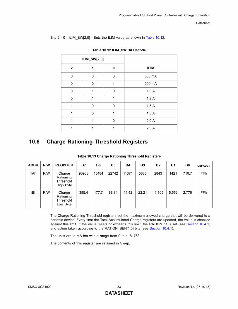
Programmable USB Port Power Controller with Charger Emulation
Datasheet
Bits 2 - 0 - ILIM_SW[2:0] - Sets the ILIM value as shown in Table 10.12.
10.6 Charge Rationing Threshold Registers
The Charge Rationing Threshold registers set the maximum allowed charge that will be delivered to aportable device. Every time the Total Accumulated Charge registers are updated, the value is checkedagainst this limit. If the value meets or exceeds this limit, the RATION bit is set (see Section 10.4.1)and action taken according to the RATION_BEH[1:0] bits (see Section 10.4.1).
The units are in mA-hrs with a range from 0 to ~181768.
The contents of this register are retained in Sleep.
Table 10.12 ILIM_SW Bit Decode
ILIM_SW[2:0]
ILIM2 1 0
0 0 0 500 mA
0 0 1 900 mA
0 1 0 1.0 A
0 1 1 1.2 A
1 0 0 1.5 A
1 0 1 1.8 A
1 1 0 2.0 A
1 1 1 2.5 A
Table 10.13 Charge Rationing Threshold Registers
ADDR R/W REGISTER B7 B6 B5 B4 B3 B2 B1 B0 DEFAULT
1Ah R/W Charge Rationing Threshold High Byte
90968 45484 22742 11371 5685 2843 1421 710.7 FFh
1Bh R/W Charge Rationing Threshold Low Byte
355.4 177.7 88.84 44.42 22.21 11.105 5.552 2.776 FFh
SMSC UCS1002 83 Revision 1.4 (07-16-13)
DATASHEET
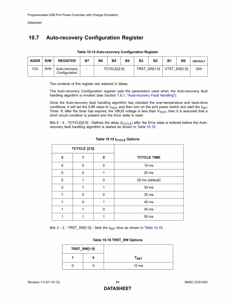
Programmable USB Port Power Controller with Charger Emulation
Datasheet
10.7 Auto-recovery Configuration Register
The contents of this register are retained in Sleep.
The Auto-recovery Configuration register sets the parameters used when the Auto-recovery faulthandling algorithm is invoked (see Section 7.6.1, "Auto-recovery Fault Handling").
Once the Auto-recovery fault handling algorithm has checked the over-temperature and back-driveconditions, it will set the ILIM value to ITEST and then turn on the port power switch and start the tRSTTimer. If, after the timer has expired, the VBUS voltage is less than VTEST, then it is assumed that ashort circuit condition is present and the Error state is reset.
Bits 6 - 4 - TCYCLE[2:0] - Defines the delay (tCYCLE) after the Error state is entered before the Auto-recovery fault handling algorithm is started as shown in Table 10.15.
Bits 3 - 2 - TRST_SW[1:0] - Sets the tRST time as shown in Table 10.16.
Table 10.14 Auto-recovery Configuration Register
ADDR R/W REGISTER B7 B6 B5 B4 B3 B2 B1 B0 DEFAULT
1Ch R/W Auto-recovery Configuration
- TCYCLE[2:0] TRST_SW[1:0] VTST_SW[1:0] 2Ah
Table 10.15 tCYCLE Options
TCYCLE [2:0]
TCYCLE TIME2 1 0
0 0 0 15 ms
0 0 1 20 ms
0 1 0 25 ms (default)
0 1 1 30 ms
1 0 0 35 ms
1 0 1 40 ms
1 1 0 45 ms
1 1 1 50 ms
Table 10.16 TRST_SW Options
TRST_SW[1:0]
TRST1 0
0 0 10 ms
Revision 1.4 (07-16-13) 84 SMSC UCS1002
DATASHEET
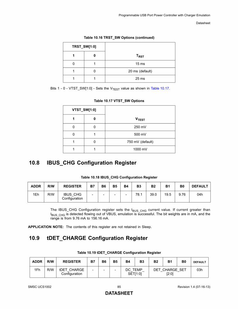
Programmable USB Port Power Controller with Charger Emulation
Datasheet
Bits 1 - 0 - VTST_SW[1:0] - Sets the VTEST value as shown in Table 10.17.
10.8 IBUS_CHG Configuration Register
The IBUS_CHG Configuration register sets the IBUS_CHG current value. If current greater thanIBUS_CHG is detected flowing out of VBUS, emulation is successful. The bit weights are in mA, and therange is from 9.76 mA to 156.16 mA.
APPLICATION NOTE: The contents of this register are not retained in Sleep.
10.9 tDET_CHARGE Configuration Register
0 1 15 ms
1 0 20 ms (default)
1 1 25 ms
Table 10.17 VTST_SW Options
VTST_SW[1:0]
VTEST1 0
0 0 250 mV
0 1 500 mV
1 0 750 mV (default)
1 1 1000 mV
Table 10.18 IBUS_CHG Configuration Register
ADDR R/W REGISTER B7 B6 B5 B4 B3 B2 B1 B0 DEFAULT
1Eh R/W IBUS_CHG Configuration
- - - - 78.1 39.0 19.5 9.76 04h
Table 10.19 tDET_CHARGE Configuration Register
ADDR R/W REGISTER B7 B6 B5 B4 B3 B2 B1 B0 DEFAULT
1Fh R/W tDET_CHARGE Configuration
- - - DC_TEMP_ SET[1:0]
DET_CHARGE_SET [2:0]
03h
Table 10.16 TRST_SW Options (continued)
TRST_SW[1:0]
TRST1 0
SMSC UCS1002 85 Revision 1.4 (07-16-13)
DATASHEET
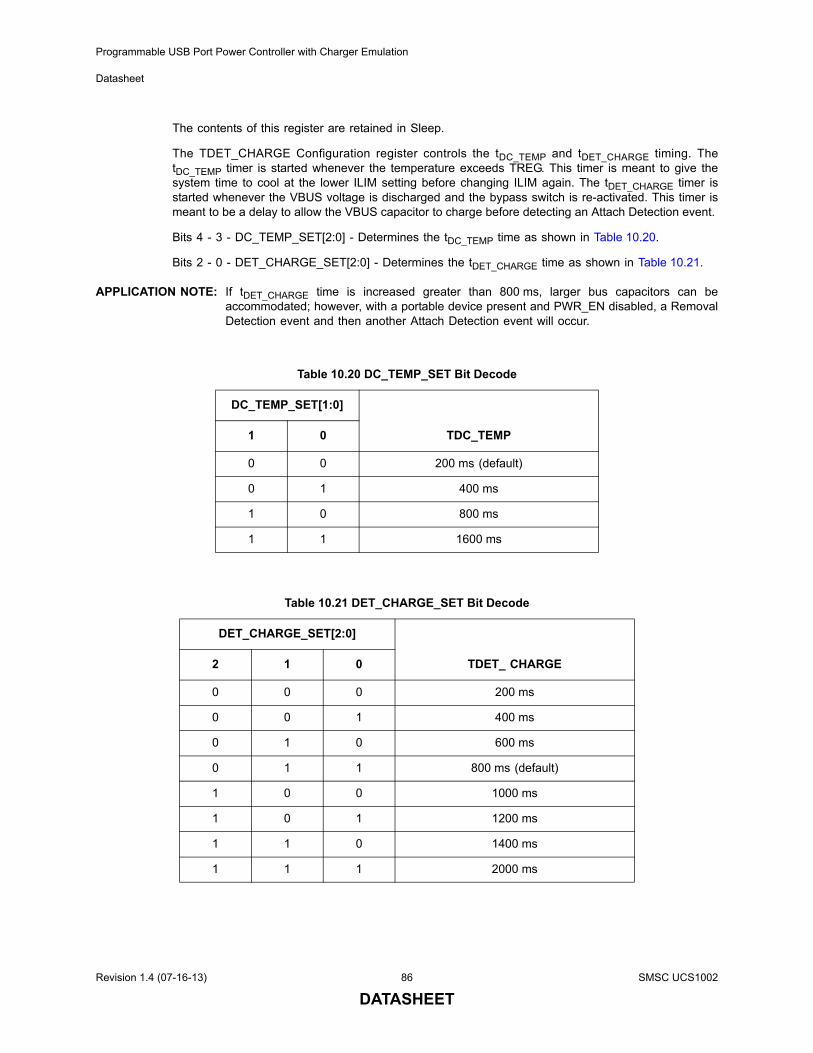
Programmable USB Port Power Controller with Charger Emulation
Datasheet
The contents of this register are retained in Sleep.
The TDET_CHARGE Configuration register controls the tDC_TEMP and tDET_CHARGE timing. ThetDC_TEMP timer is started whenever the temperature exceeds TREG. This timer is meant to give thesystem time to cool at the lower ILIM setting before changing ILIM again. The tDET_CHARGE timer isstarted whenever the VBUS voltage is discharged and the bypass switch is re-activated. This timer ismeant to be a delay to allow the VBUS capacitor to charge before detecting an Attach Detection event.
Bits 4 - 3 - DC_TEMP_SET[2:0] - Determines the tDC_TEMP time as shown in Table 10.20.
Bits 2 - 0 - DET_CHARGE_SET[2:0] - Determines the tDET_CHARGE time as shown in Table 10.21.
APPLICATION NOTE: If tDET_CHARGE time is increased greater than 800 ms, larger bus capacitors can beaccommodated; however, with a portable device present and PWR_EN disabled, a RemovalDetection event and then another Attach Detection event will occur.
Table 10.20 DC_TEMP_SET Bit Decode
DC_TEMP_SET[1:0]
TDC_TEMP1 0
0 0 200 ms (default)
0 1 400 ms
1 0 800 ms
1 1 1600 ms
Table 10.21 DET_CHARGE_SET Bit Decode
DET_CHARGE_SET[2:0]
TDET_ CHARGE2 1 0
0 0 0 200 ms
0 0 1 400 ms
0 1 0 600 ms
0 1 1 800 ms (default)
1 0 0 1000 ms
1 0 1 1200 ms
1 1 0 1400 ms
1 1 1 2000 ms
Revision 1.4 (07-16-13) 86 SMSC UCS1002
DATASHEET
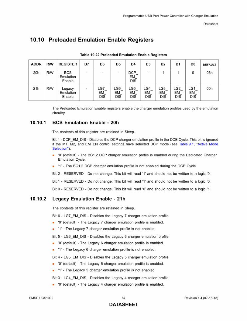
Programmable USB Port Power Controller with Charger Emulation
Datasheet
10.10 Preloaded Emulation Enable Registers
The Preloaded Emulation Enable registers enable the charger emulation profiles used by the emulationcircuitry.
10.10.1 BCS Emulation Enable - 20h
The contents of this register are retained in Sleep.
Bit 4 - DCP_EM_DIS - Disables the DCP charger emulation profile in the DCE Cycle. This bit is ignoredif the M1, M2, and EM_EN control settings have selected DCP mode (see Table 9.1, "Active ModeSelection").
‘0’ (default) - The BC1.2 DCP charger emulation profile is enabled during the Dedicated Charger Emulation Cycle.
‘1’ - The BC1.2 DCP charger emulation profile is not enabled during the DCE Cycle.
Bit 2 - RESERVED - Do not change. This bit will read ‘1’ and should not be written to a logic ‘0’.
Bit 1 - RESERVED - Do not change. This bit will read ‘1’ and should not be written to a logic ‘0’.
Bit 0 - RESERVED - Do not change. This bit will read ‘0’ and should not be written to a logic ‘1’.
10.10.2 Legacy Emulation Enable - 21h
The contents of this register are retained in Sleep.
Bit 6 - LG7_EM_DIS - Disables the Legacy 7 charger emulation profile.
‘0’ (default) - The Legacy 7 charger emulation profile is enabled.
‘1’ - The Legacy 7 charger emulation profile is not enabled.
Bit 5 - LG6_EM_DIS - Disables the Legacy 6 charger emulation profile.
‘0’ (default) - The Legacy 6 charger emulation profile is enabled.
‘1’ - The Legacy 6 charger emulation profile is not enabled.
Bit 4 - LG5_EM_DIS - Disables the Legacy 5 charger emulation profile.
‘0’ (default) - The Legacy 5 charger emulation profile is enabled.
‘1’ - The Legacy 5 charger emulation profile is not enabled.
Bit 3 - LG4_EM_DIS - Disables the Legacy 4 charger emulation profile.
‘0’ (default) - The Legacy 4 charger emulation profile is enabled.
Table 10.22 Preloaded Emulation Enable Registers
ADDR R/W REGISTER B7 B6 B5 B4 B3 B2 B1 B0 DEFAULT
20h R/W BCS Emulation
Enable
- - - DCP_EM_ DIS
- 1 1 0 06h
21h R/W Legacy Emulation
Enable
- LG7_ EM_ DIS
LG6_EM_ DIS
LG5_EM_ DIS
LG4_EM_ DIS
LG3_EM_ DIS
LG2_EM_ DIS
LG1_EM_ DIS
00h
SMSC UCS1002 87 Revision 1.4 (07-16-13)
DATASHEET
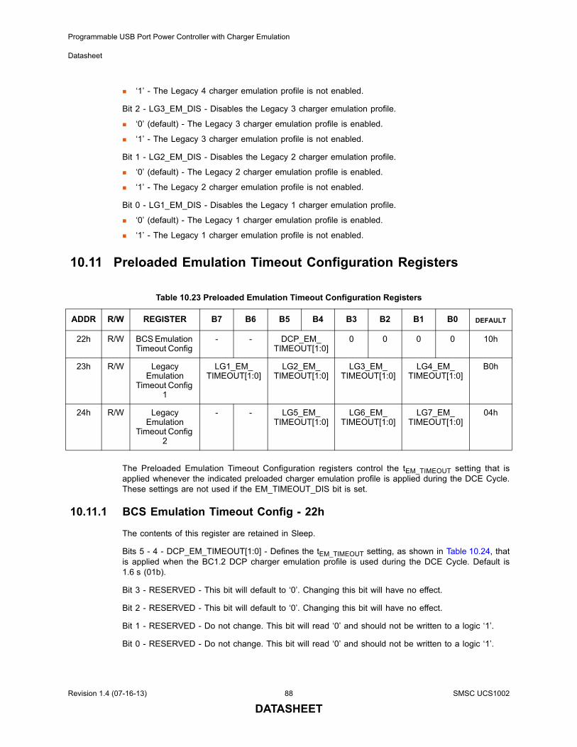
Programmable USB Port Power Controller with Charger Emulation
Datasheet
‘1’ - The Legacy 4 charger emulation profile is not enabled.
Bit 2 - LG3_EM_DIS - Disables the Legacy 3 charger emulation profile.
‘0’ (default) - The Legacy 3 charger emulation profile is enabled.
‘1’ - The Legacy 3 charger emulation profile is not enabled.
Bit 1 - LG2_EM_DIS - Disables the Legacy 2 charger emulation profile.
‘0’ (default) - The Legacy 2 charger emulation profile is enabled.
‘1’ - The Legacy 2 charger emulation profile is not enabled.
Bit 0 - LG1_EM_DIS - Disables the Legacy 1 charger emulation profile.
‘0’ (default) - The Legacy 1 charger emulation profile is enabled.
‘1’ - The Legacy 1 charger emulation profile is not enabled.
10.11 Preloaded Emulation Timeout Configuration Registers
The Preloaded Emulation Timeout Configuration registers control the tEM_TIMEOUT setting that isapplied whenever the indicated preloaded charger emulation profile is applied during the DCE Cycle.These settings are not used if the EM_TIMEOUT_DIS bit is set.
10.11.1 BCS Emulation Timeout Config - 22h
The contents of this register are retained in Sleep.
Bits 5 - 4 - DCP_EM_TIMEOUT[1:0] - Defines the tEM_TIMEOUT setting, as shown in Table 10.24, thatis applied when the BC1.2 DCP charger emulation profile is used during the DCE Cycle. Default is1.6 s (01b).
Bit 3 - RESERVED - This bit will default to ‘0’. Changing this bit will have no effect.
Bit 2 - RESERVED - This bit will default to ‘0’. Changing this bit will have no effect.
Bit 1 - RESERVED - Do not change. This bit will read ‘0’ and should not be written to a logic ‘1’.
Bit 0 - RESERVED - Do not change. This bit will read ‘0’ and should not be written to a logic ‘1’.
Table 10.23 Preloaded Emulation Timeout Configuration Registers
ADDR R/W REGISTER B7 B6 B5 B4 B3 B2 B1 B0 DEFAULT
22h R/W BCS Emulation Timeout Config
- - DCP_EM_ TIMEOUT[1:0]
0 0 0 0 10h
23h R/W Legacy Emulation
Timeout Config 1
LG1_EM_ TIMEOUT[1:0]
LG2_EM_ TIMEOUT[1:0]
LG3_EM_ TIMEOUT[1:0]
LG4_EM_ TIMEOUT[1:0]
B0h
24h R/W Legacy Emulation
Timeout Config 2
- - LG5_EM_ TIMEOUT[1:0]
LG6_EM_ TIMEOUT[1:0]
LG7_EM_ TIMEOUT[1:0]
04h
Revision 1.4 (07-16-13) 88 SMSC UCS1002
DATASHEET
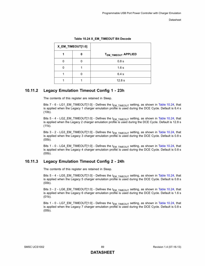
Programmable USB Port Power Controller with Charger Emulation
Datasheet
10.11.2 Legacy Emulation Timeout Config 1 - 23h
The contents of this register are retained in Sleep.
Bits 7 - 6 - LG1_EM_TIMEOUT[1:0] - Defines the tEM_TIMEOUT setting, as shown in Table 10.24, thatis applied when the Legacy 1 charger emulation profile is used during the DCE Cycle. Default is 6.4 s(10b).
Bits 5 - 4 - LG2_EM_TIMEOUT[1:0] - Defines the tEM_TIMEOUT setting, as shown in Table 10.24, thatis applied when the Legacy 2 charger emulation profile is used during the DCE Cycle. Default is 12.8 s(11b).
Bits 3 - 2 - LG3_EM_TIMEOUT[1:0] - Defines the tEM_TIMEOUT setting, as shown in Table 10.24, thatis applied when the Legacy 3 charger emulation profile is used during the DCE Cycle. Default is 0.8 s(00b).
Bits 1 - 0 - LG4_EM_TIMEOUT[1:0] - Defines the tEM_TIMEOUT setting, as shown in Table 10.24, thatis applied when the Legacy 4 charger emulation profile is used during the DCE Cycle. Default is 0.8 s(00b).
10.11.3 Legacy Emulation Timeout Config 2 - 24h
The contents of this register are retained in Sleep.
Bits 5 - 4 - LG5_EM_TIMEOUT[1:0] - Defines the tEM_TIMEOUT setting, as shown in Table 10.24, thatis applied when the Legacy 5 charger emulation profile is used during the DCE Cycle. Default is 0.8 s(00b).
Bits 3 - 2 - LG6_EM_TIMEOUT[1:0] - Defines the tEM_TIMEOUT setting, as shown in Table 10.24, thatis applied when the Legacy 6 charger emulation profile is used during the DCE Cycle. Default is 1.6 s(01b).
Bits 1 - 0 - LG7_EM_TIMEOUT[1:0] - Defines the tEM_TIMEOUT setting, as shown in Table 10.24, thatis applied when the Legacy 7 charger emulation profile is used during the DCE Cycle. Default is 0.8 s(00b).
Table 10.24 X_EM_TIMEOUT Bit Decode
X_EM_TIMEOUT[1:0]
TEM_TIMEOUT APPLIED1 0
0 0 0.8 s
0 1 1.6 s
1 0 6.4 s
1 1 12.8 s
SMSC UCS1002 89 Revision 1.4 (07-16-13)
DATASHEET
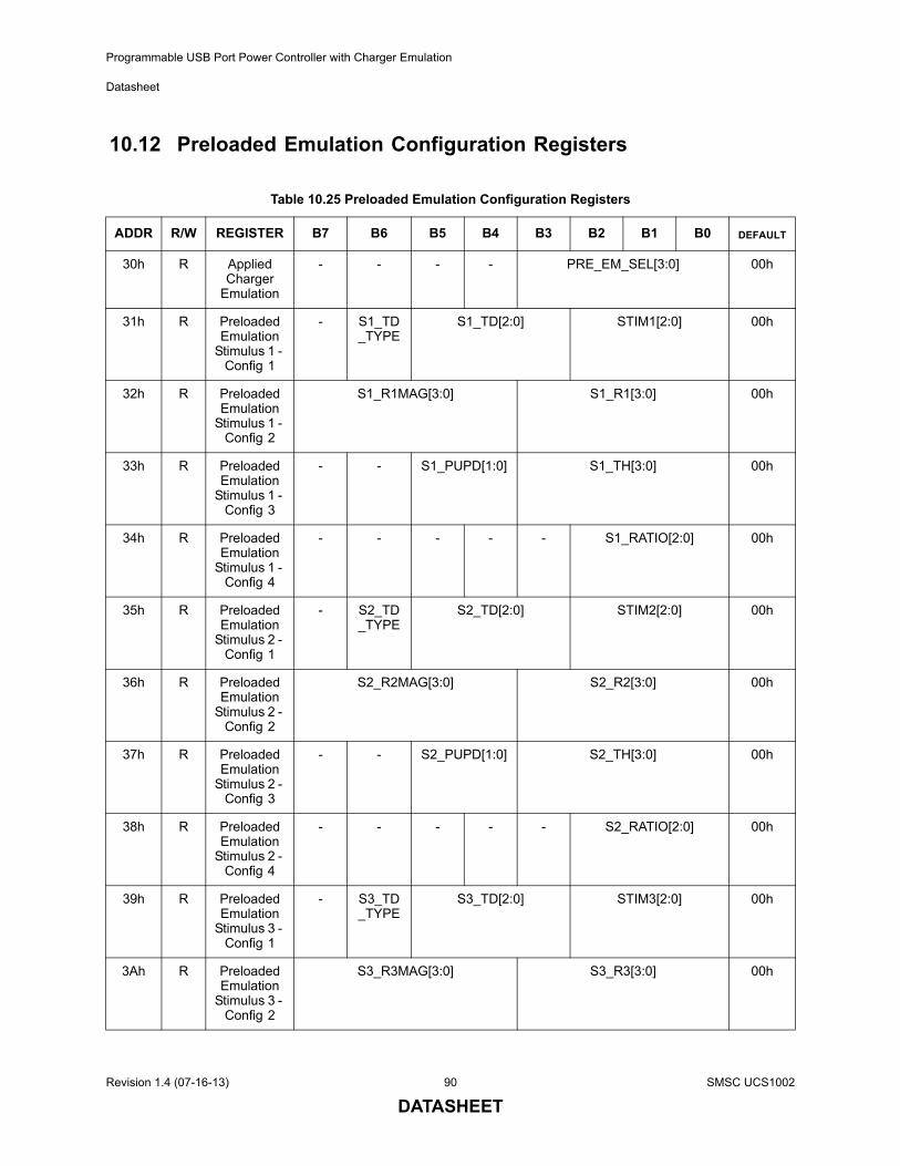
Programmable USB Port Power Controller with Charger Emulation
Datasheet
10.12 Preloaded Emulation Configuration Registers
Table 10.25 Preloaded Emulation Configuration Registers
ADDR R/W REGISTER B7 B6 B5 B4 B3 B2 B1 B0 DEFAULT
30h R Applied Charger
Emulation
- - - - PRE_EM_SEL[3:0] 00h
31h R Preloaded Emulation
Stimulus 1 - Config 1
- S1_TD_TYPE
S1_TD[2:0] STIM1[2:0] 00h
32h R Preloaded Emulation
Stimulus 1 - Config 2
S1_R1MAG[3:0] S1_R1[3:0] 00h
33h R Preloaded Emulation
Stimulus 1 - Config 3
- - S1_PUPD[1:0] S1_TH[3:0] 00h
34h R Preloaded Emulation
Stimulus 1 - Config 4
- - - - - S1_RATIO[2:0] 00h
35h R Preloaded Emulation
Stimulus 2 - Config 1
- S2_TD_TYPE
S2_TD[2:0] STIM2[2:0] 00h
36h R Preloaded Emulation
Stimulus 2 - Config 2
S2_R2MAG[3:0] S2_R2[3:0] 00h
37h R Preloaded Emulation
Stimulus 2 - Config 3
- - S2_PUPD[1:0] S2_TH[3:0] 00h
38h R Preloaded Emulation
Stimulus 2 - Config 4
- - - - - S2_RATIO[2:0] 00h
39h R Preloaded Emulation
Stimulus 3 - Config 1
- S3_TD_TYPE
S3_TD[2:0] STIM3[2:0] 00h
3Ah R Preloaded Emulation
Stimulus 3 - Config 2
S3_R3MAG[3:0] S3_R3[3:0] 00h
Revision 1.4 (07-16-13) 90 SMSC UCS1002
DATASHEET
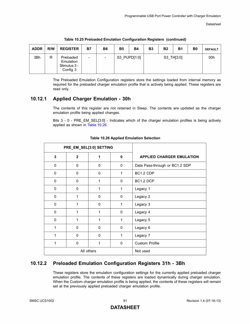
Programmable USB Port Power Controller with Charger Emulation
Datasheet
The Preloaded Emulation Configuration registers store the settings loaded from internal memory asrequired for the preloaded charger emulation profile that is actively being applied. These registers areread only.
10.12.1 Applied Charger Emulation - 30h
The contents of this register are not retained in Sleep. The contents are updated as the chargeremulation profile being applied changes.
Bits 3 - 0 - PRE_EM_SEL[3:0] - Indicates which of the charger emulation profiles is being activelyapplied as shown in Table 10.26.
10.12.2 Preloaded Emulation Configuration Registers 31h - 3Bh
These registers store the emulation configuration settings for the currently applied preloaded chargeremulation profile. The contents of these registers are loaded dynamically during charger emulation.When the Custom charger emulation profile is being applied, the contents of these registers will remainset at the previously applied preloaded charger emulation profile.
3Bh R Preloaded Emulation
Stimulus 3 - Config 3
- - S3_PUPD[1:0] S3_TH[3:0] 00h
Table 10.26 Applied Emulation Selection
PRE_EM_SEL[3:0] SETTING
APPLIED CHARGER EMULATION3 2 1 0
0 0 0 0 Data Pass-through or BC1.2 SDP
0 0 0 1 BC1.2 CDP
0 0 1 0 BC1.2 DCP
0 0 1 1 Legacy 1
0 1 0 0 Legacy 2
0 1 0 1 Legacy 3
0 1 1 0 Legacy 4
0 1 1 1 Legacy 5
1 0 0 0 Legacy 6
1 0 0 1 Legacy 7
1 0 1 0 Custom Profile
All others Not used
Table 10.25 Preloaded Emulation Configuration Registers (continued)
ADDR R/W REGISTER B7 B6 B5 B4 B3 B2 B1 B0 DEFAULT
SMSC UCS1002 91 Revision 1.4 (07-16-13)
DATASHEET
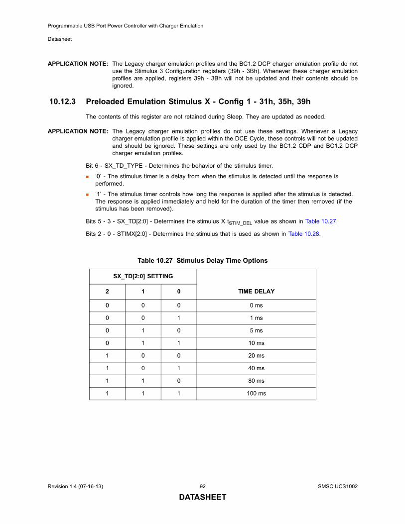
Programmable USB Port Power Controller with Charger Emulation
Datasheet
APPLICATION NOTE: The Legacy charger emulation profiles and the BC1.2 DCP charger emulation profile do notuse the Stimulus 3 Configuration registers (39h - 3Bh). Whenever these charger emulationprofiles are applied, registers 39h - 3Bh will not be updated and their contents should beignored.
10.12.3 Preloaded Emulation Stimulus X - Config 1 - 31h, 35h, 39h
The contents of this register are not retained during Sleep. They are updated as needed.
APPLICATION NOTE: The Legacy charger emulation profiles do not use these settings. Whenever a Legacycharger emulation profile is applied within the DCE Cycle, these controls will not be updatedand should be ignored. These settings are only used by the BC1.2 CDP and BC1.2 DCPcharger emulation profiles.
Bit 6 - SX_TD_TYPE - Determines the behavior of the stimulus timer.
‘0’ - The stimulus timer is a delay from when the stimulus is detected until the response is performed.
‘1’ - The stimulus timer controls how long the response is applied after the stimulus is detected. The response is applied immediately and held for the duration of the timer then removed (if the stimulus has been removed).
Bits 5 - 3 - SX_TD[2:0] - Determines the stimulus X tSTIM_DEL value as shown in Table 10.27.
Bits 2 - 0 - STIMX[2:0] - Determines the stimulus that is used as shown in Table 10.28.
Table 10.27 Stimulus Delay Time Options
SX_TD[2:0] SETTING
TIME DELAY2 1 0
0 0 0 0 ms
0 0 1 1 ms
0 1 0 5 ms
0 1 1 10 ms
1 0 0 20 ms
1 0 1 40 ms
1 1 0 80 ms
1 1 1 100 ms
Revision 1.4 (07-16-13) 92 SMSC UCS1002
DATASHEET
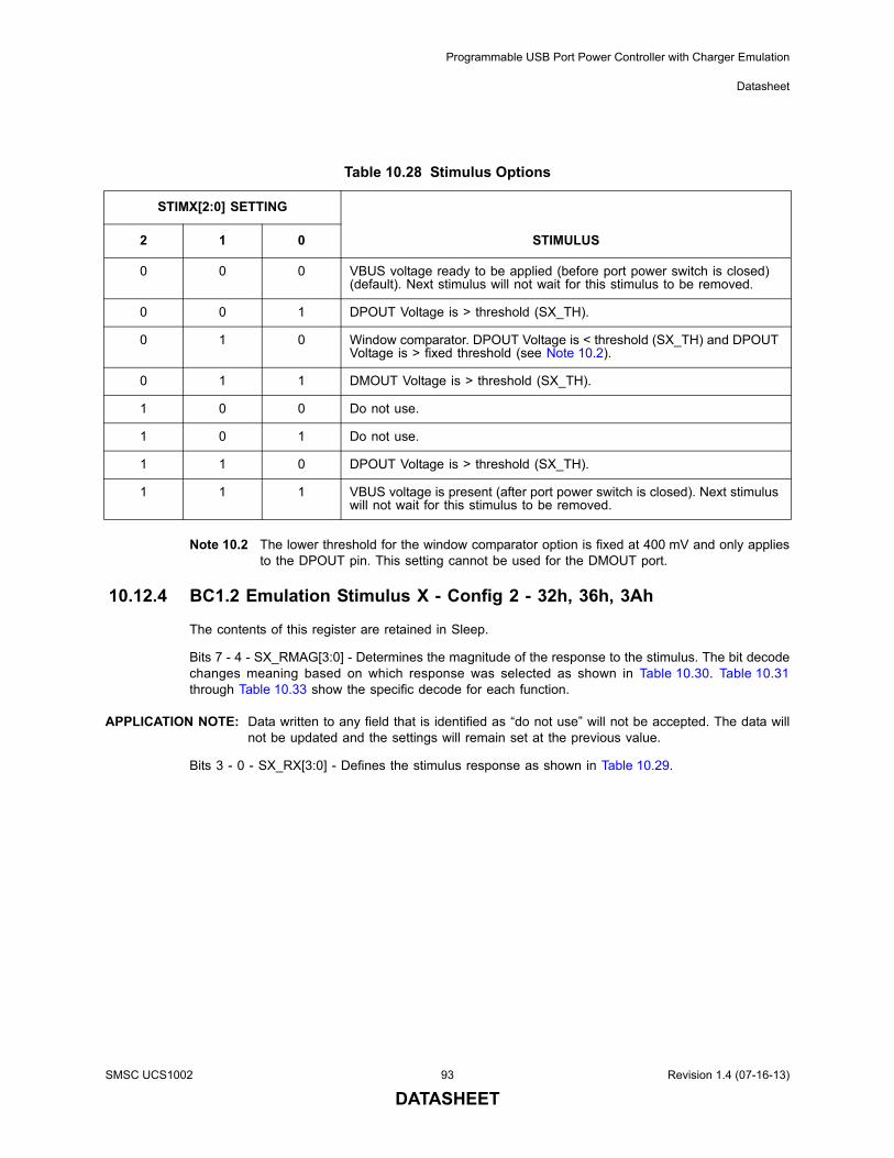
Programmable USB Port Power Controller with Charger Emulation
Datasheet
Note 10.2 The lower threshold for the window comparator option is fixed at 400 mV and only appliesto the DPOUT pin. This setting cannot be used for the DMOUT port.
10.12.4 BC1.2 Emulation Stimulus X - Config 2 - 32h, 36h, 3Ah
The contents of this register are retained in Sleep.
Bits 7 - 4 - SX_RMAG[3:0] - Determines the magnitude of the response to the stimulus. The bit decodechanges meaning based on which response was selected as shown in Table 10.30. Table 10.31through Table 10.33 show the specific decode for each function.
APPLICATION NOTE: Data written to any field that is identified as “do not use” will not be accepted. The data willnot be updated and the settings will remain set at the previous value.
Bits 3 - 0 - SX_RX[3:0] - Defines the stimulus response as shown in Table 10.29.
Table 10.28 Stimulus Options
STIMX[2:0] SETTING
STIMULUS2 1 0
0 0 0 VBUS voltage ready to be applied (before port power switch is closed) (default). Next stimulus will not wait for this stimulus to be removed.
0 0 1 DPOUT Voltage is > threshold (SX_TH).
0 1 0 Window comparator. DPOUT Voltage is < threshold (SX_TH) and DPOUT Voltage is > fixed threshold (see Note 10.2).
0 1 1 DMOUT Voltage is > threshold (SX_TH).
1 0 0 Do not use.
1 0 1 Do not use.
1 1 0 DPOUT Voltage is > threshold (SX_TH).
1 1 1 VBUS voltage is present (after port power switch is closed). Next stimulus will not wait for this stimulus to be removed.
SMSC UCS1002 93 Revision 1.4 (07-16-13)
DATASHEET
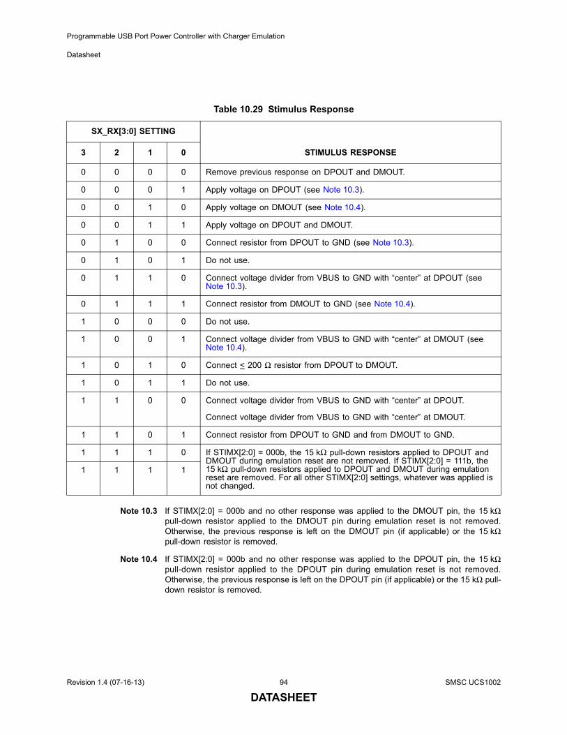
Programmable USB Port Power Controller with Charger Emulation
Datasheet
Note 10.3 If STIMX[2:0] = 000b and no other response was applied to the DMOUT pin, the 15 kΩpull-down resistor applied to the DMOUT pin during emulation reset is not removed.Otherwise, the previous response is left on the DMOUT pin (if applicable) or the 15 kΩpull-down resistor is removed.
Note 10.4 If STIMX[2:0] = 000b and no other response was applied to the DPOUT pin, the 15 kΩpull-down resistor applied to the DPOUT pin during emulation reset is not removed.Otherwise, the previous response is left on the DPOUT pin (if applicable) or the 15 kΩ pull-down resistor is removed.
Table 10.29 Stimulus Response
SX_RX[3:0] SETTING
STIMULUS RESPONSE3 2 1 0
0 0 0 0 Remove previous response on DPOUT and DMOUT.
0 0 0 1 Apply voltage on DPOUT (see Note 10.3).
0 0 1 0 Apply voltage on DMOUT (see Note 10.4).
0 0 1 1 Apply voltage on DPOUT and DMOUT.
0 1 0 0 Connect resistor from DPOUT to GND (see Note 10.3).
0 1 0 1 Do not use.
0 1 1 0 Connect voltage divider from VBUS to GND with “center” at DPOUT (see Note 10.3).
0 1 1 1 Connect resistor from DMOUT to GND (see Note 10.4).
1 0 0 0 Do not use.
1 0 0 1 Connect voltage divider from VBUS to GND with “center” at DMOUT (see Note 10.4).
1 0 1 0 Connect < 200 Ω resistor from DPOUT to DMOUT.
1 0 1 1 Do not use.
1 1 0 0 Connect voltage divider from VBUS to GND with “center” at DPOUT.
Connect voltage divider from VBUS to GND with “center” at DMOUT.
1 1 0 1 Connect resistor from DPOUT to GND and from DMOUT to GND.
1 1 1 0 If STIMX[2:0] = 000b, the 15 kΩ pull-down resistors applied to DPOUT and DMOUT during emulation reset are not removed. If STIMX[2:0] = 111b, the 15 kΩ pull-down resistors applied to DPOUT and DMOUT during emulation reset are removed. For all other STIMX[2:0] settings, whatever was applied is not changed.
1 1 1 1
Revision 1.4 (07-16-13) 94 SMSC UCS1002
DATASHEET
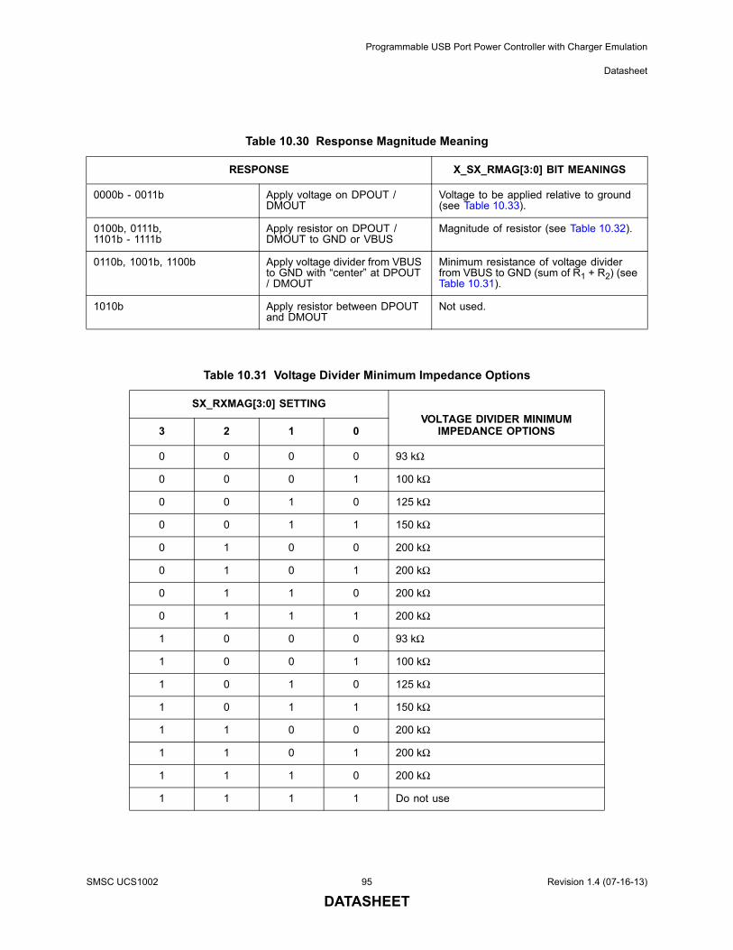
Programmable USB Port Power Controller with Charger Emulation
Datasheet
Table 10.30 Response Magnitude Meaning
RESPONSE X_SX_RMAG[3:0] BIT MEANINGS
0000b - 0011b Apply voltage on DPOUT / DMOUT
Voltage to be applied relative to ground (see Table 10.33).
0100b, 0111b, 1101b - 1111b
Apply resistor on DPOUT / DMOUT to GND or VBUS
Magnitude of resistor (see Table 10.32).
0110b, 1001b, 1100b Apply voltage divider from VBUS to GND with “center” at DPOUT / DMOUT
Minimum resistance of voltage divider from VBUS to GND (sum of R1 + R2) (see Table 10.31).
1010b Apply resistor between DPOUT and DMOUT
Not used.
Table 10.31 Voltage Divider Minimum Impedance Options
SX_RXMAG[3:0] SETTING
VOLTAGE DIVIDER MINIMUM IMPEDANCE OPTIONS 3 2 1 0
0 0 0 0 93 kΩ
0 0 0 1 100 kΩ
0 0 1 0 125 kΩ
0 0 1 1 150 kΩ
0 1 0 0 200 kΩ
0 1 0 1 200 kΩ
0 1 1 0 200 kΩ
0 1 1 1 200 kΩ
1 0 0 0 93 kΩ
1 0 0 1 100 kΩ
1 0 1 0 125 kΩ
1 0 1 1 150 kΩ
1 1 0 0 200 kΩ
1 1 0 1 200 kΩ
1 1 1 0 200 kΩ
1 1 1 1 Do not use
SMSC UCS1002 95 Revision 1.4 (07-16-13)
DATASHEET
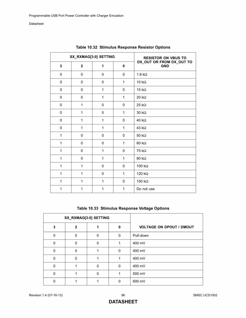
Programmable USB Port Power Controller with Charger Emulation
Datasheet
Table 10.32 Stimulus Response Resistor Options
SX_RXMAG[3:0] SETTING RESISTOR ON VBUS TO DX_OUT OR FROM DX_OUT TO
GND3 2 1 0
0 0 0 0 1.8 kΩ
0 0 0 1 10 kΩ
0 0 1 0 15 kΩ
0 0 1 1 20 kΩ
0 1 0 0 25 kΩ
0 1 0 1 30 kΩ
0 1 1 0 40 kΩ
0 1 1 1 43 kΩ
1 0 0 0 50 kΩ
1 0 0 1 60 kΩ
1 0 1 0 75 kΩ
1 0 1 1 80 kΩ
1 1 0 0 100 kΩ
1 1 0 1 120 kΩ
1 1 1 0 150 kΩ
1 1 1 1 Do not use
Table 10.33 Stimulus Response Voltage Options
SX_RXMAG[3:0] SETTING
VOLTAGE ON DPOUT / DMOUT 3 2 1 0
0 0 0 0 Pull-down
0 0 0 1 400 mV
0 0 1 0 400 mV
0 0 1 1 400 mV
0 1 0 0 400 mV
0 1 0 1 500 mV
0 1 1 0 600 mV
Revision 1.4 (07-16-13) 96 SMSC UCS1002
DATASHEET
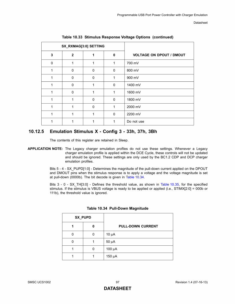
Programmable USB Port Power Controller with Charger Emulation
Datasheet
10.12.5 Emulation Stimulus X - Config 3 - 33h, 37h, 3Bh
The contents of this register are retained in Sleep.
APPLICATION NOTE: The Legacy charger emulation profiles do not use these settings. Whenever a Legacycharger emulation profile is applied within the DCE Cycle, these controls will not be updatedand should be ignored. These settings are only used by the BC1.2 CDP and DCP chargeremulation profiles.
Bits 5 - 4 - SX_PUPD[1:0] - Determines the magnitude of the pull-down current applied on the DPOUTand DMOUT pins when the stimulus response is to apply a voltage and the voltage magnitude is setat pull-down (0000b). The bit decode is given in Table 10.34.
Bits 3 - 0 - SX_TH[3:0] - Defines the threshold value, as shown in Table 10.35, for the specifiedstimulus. If the stimulus is VBUS voltage is ready to be applied or applied (i.e., STIMX[2:0] = 000b or111b), the threshold value is ignored.
0 1 1 1 700 mV
1 0 0 0 800 mV
1 0 0 1 900 mV
1 0 1 0 1400 mV
1 0 1 1 1600 mV
1 1 0 0 1800 mV
1 1 0 1 2000 mV
1 1 1 0 2200 mV
1 1 1 1 Do not use
Table 10.34 Pull-Down Magnitude
SX_PUPD
PULL-DOWN CURRENT1 0
0 0 10 μA
0 1 50 μA
1 0 100 μA
1 1 150 μA
Table 10.33 Stimulus Response Voltage Options (continued)
SX_RXMAG[3:0] SETTING
VOLTAGE ON DPOUT / DMOUT 3 2 1 0
SMSC UCS1002 97 Revision 1.4 (07-16-13)
DATASHEET
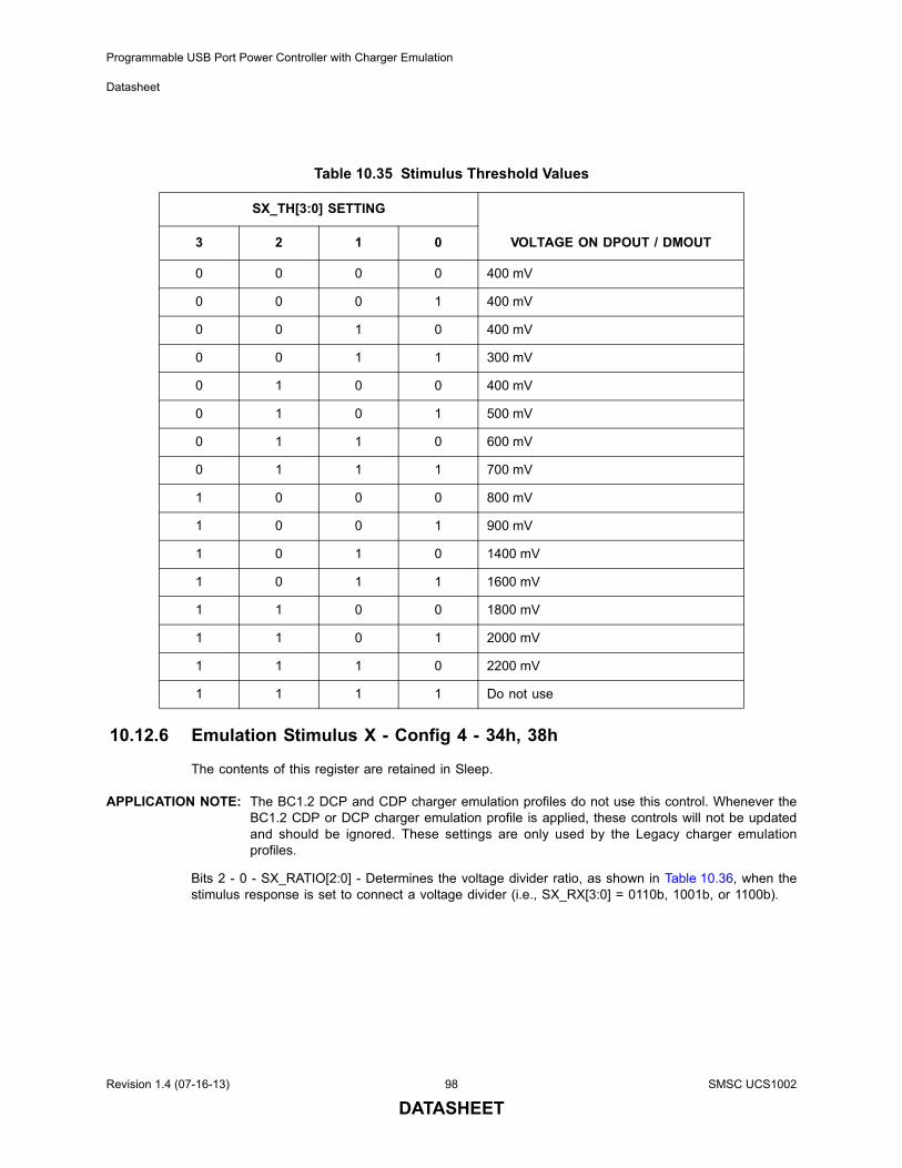
Programmable USB Port Power Controller with Charger Emulation
Datasheet
10.12.6 Emulation Stimulus X - Config 4 - 34h, 38h
The contents of this register are retained in Sleep.
APPLICATION NOTE: The BC1.2 DCP and CDP charger emulation profiles do not use this control. Whenever theBC1.2 CDP or DCP charger emulation profile is applied, these controls will not be updatedand should be ignored. These settings are only used by the Legacy charger emulationprofiles.
Bits 2 - 0 - SX_RATIO[2:0] - Determines the voltage divider ratio, as shown in Table 10.36, when thestimulus response is set to connect a voltage divider (i.e., SX_RX[3:0] = 0110b, 1001b, or 1100b).
Table 10.35 Stimulus Threshold Values
SX_TH[3:0] SETTING
VOLTAGE ON DPOUT / DMOUT 3 2 1 0
0 0 0 0 400 mV
0 0 0 1 400 mV
0 0 1 0 400 mV
0 0 1 1 300 mV
0 1 0 0 400 mV
0 1 0 1 500 mV
0 1 1 0 600 mV
0 1 1 1 700 mV
1 0 0 0 800 mV
1 0 0 1 900 mV
1 0 1 0 1400 mV
1 0 1 1 1600 mV
1 1 0 0 1800 mV
1 1 0 1 2000 mV
1 1 1 0 2200 mV
1 1 1 1 Do not use
Revision 1.4 (07-16-13) 98 SMSC UCS1002
DATASHEET
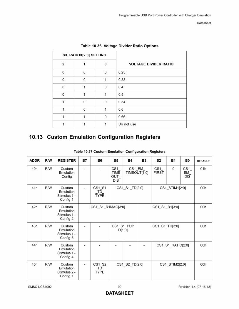
Programmable USB Port Power Controller with Charger Emulation
Datasheet
10.13 Custom Emulation Configuration Registers
Table 10.36 Voltage Divider Ratio Options
SX_RATIOX[2:0] SETTING
VOLTAGE DIVIDER RATIO2 1 0
0 0 0 0.25
0 0 1 0.33
0 1 0 0.4
0 1 1 0.5
1 0 0 0.54
1 0 1 0.6
1 1 0 0.66
1 1 1 Do not use
Table 10.37 Custom Emulation Configuration Registers
ADDR R/W REGISTER B7 B6 B5 B4 B3 B2 B1 B0 DEFAULT
40h R/W Custom Emulation
Config
- - CS1_TIMEOUT_DIS
CS1_EM_ TIMEOUT[1:0]
CS1_FIRST
0 CS1_EM_ DIS
01h
41h R/W Custom Emulation
Stimulus 1 - Config 1
- CS1_S1_TD_ TYPE
CS1_S1_TD[2:0] CS1_STIM1[2:0] 00h
42h R/W Custom Emulation
Stimulus 1 - Config 2
CS1_S1_R1MAG[3:0] CS1_S1_R1[3:0] 00h
43h R/W Custom Emulation
Stimulus 1 - Config 3
- - CS1_S1_PUPD[1:0]
CS1_S1_TH[3:0] 00h
44h R/W Custom Emulation
Stimulus 1 - Config 4
- - - - - CS1_S1_RATIO[2:0] 00h
45h R/W Custom Emulation
Stimulus 2 - Config 1
- CS1_S2_TD_ TYPE
CS1_S2_TD[2:0] CS1_STIM2[2:0] 00h
SMSC UCS1002 99 Revision 1.4 (07-16-13)
DATASHEET
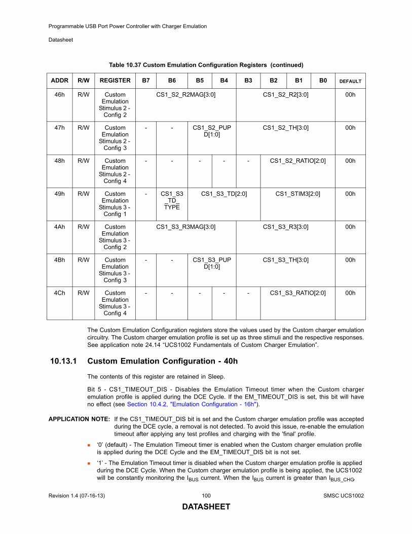
Programmable USB Port Power Controller with Charger Emulation
Datasheet
The Custom Emulation Configuration registers store the values used by the Custom charger emulationcircuitry. The Custom charger emulation profile is set up as three stimuli and the respective responses.See application note 24.14 “UCS1002 Fundamentals of Custom Charger Emulation”.
10.13.1 Custom Emulation Configuration - 40h
The contents of this register are retained in Sleep.
Bit 5 - CS1_TIMEOUT_DIS - Disables the Emulation Timeout timer when the Custom chargeremulation profile is applied during the DCE Cycle. If the EM_TIMEOUT_DIS is set, this bit will haveno effect (see Section 10.4.2, "Emulation Configuration - 16h").
APPLICATION NOTE: If the CS1_TIMEOUT_DIS bit is set and the Custom charger emulation profile was acceptedduring the DCE cycle, a removal is not detected. To avoid this issue, re-enable the emulationtimeout after applying any test profiles and charging with the 'final' profile.
‘0’ (default) - The Emulation Timeout timer is enabled when the Custom charger emulation profile is applied during the DCE Cycle and the EM_TIMEOUT_DIS bit is not set.
‘1’ - The Emulation Timeout timer is disabled when the Custom charger emulation profile is applied during the DCE Cycle. When the Custom charger emulation profile is being applied, the UCS1002 will be constantly monitoring the IBUS current. When the IBUS current is greater than IBUS_CHG,
46h R/W Custom Emulation
Stimulus 2 - Config 2
CS1_S2_R2MAG[3:0] CS1_S2_R2[3:0] 00h
47h R/W Custom Emulation
Stimulus 2 - Config 3
- - CS1_S2_PUPD[1:0]
CS1_S2_TH[3:0] 00h
48h R/W Custom Emulation
Stimulus 2 - Config 4
- - - - - CS1_S2_RATIO[2:0] 00h
49h R/W Custom Emulation
Stimulus 3 - Config 1
- CS1_S3_TD_ TYPE
CS1_S3_TD[2:0] CS1_STIM3[2:0] 00h
4Ah R/W Custom Emulation
Stimulus 3 - Config 2
CS1_S3_R3MAG[3:0] CS1_S3_R3[3:0] 00h
4Bh R/W Custom Emulation
Stimulus 3 - Config 3
- - CS1_S3_PUPD[1:0]
CS1_S3_TH[3:0] 00h
4Ch R/W Custom Emulation
Stimulus 3 - Config 4
- - - - - CS1_S3_RATIO[2:0] 00h
Table 10.37 Custom Emulation Configuration Registers (continued)
ADDR R/W REGISTER B7 B6 B5 B4 B3 B2 B1 B0 DEFAULT
Revision 1.4 (07-16-13) 100 SMSC UCS1002
DATASHEET
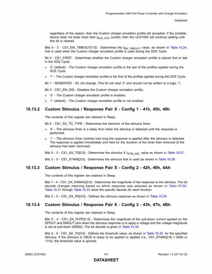
Programmable USB Port Power Controller with Charger Emulation
Datasheet
regardless of the reason, then the Custom charger emulation profile will accepted. If the portable device does not draw more than IBUS_CHG current, then the UCS1002 will continue waiting until this bit is cleared.
Bits 4 - 3 - CS1_EM_TIMEOUT[1:0] - Determines the tEM_TIMEOUT value, as shown in Table 10.24,that is used when the Custom charger emulation profile is used during the DCE Cycle.
Bit 2 - CS1_FIRST - Determines whether the Custom charger emulation profile is placed first or lastin the DCE Cycle.
‘0’ (default) - The Custom charger emulation profile is the last of the profiles applied during the DCE Cycle.
‘1’ - The Custom charger emulation profile is the first of the profiles applied during the DCE Cycle.
Bit 1 - RESERVED - Do not change. This bit will read ‘0’ and should not be written to a logic ‘1’.
Bit 0 - CS1_EM_DIS - Disables the Custom charger emulation profile.
‘0’ - The Custom charger emulation profile is enabled.
‘1’ (default) - The Custom charger emulation profile is not enabled.
10.13.2 Custom Stimulus / Response Pair X - Config 1 - 41h, 45h, 49h
The contents of this register are retained in Sleep.
Bit 6 - CS1_SX_TD_TYPE - Determines the behavior of the stimulus timer.
‘0’ - The stimulus timer is a delay from when the stimulus is detected until the response is performed.
‘1’ - The stimulus timer controls how long the response is applied after the stimulus is detected. The response is applied immediately and held for the duration of the timer then removed (if the stimulus has been removed).
Bits 5 - 3 - CS1_SX_TD[2:0] - Determines the stimulus X tSTIM_DEL value as shown in Table 10.27.
Bits 2 - 0 - CS1_STIMX[2:0] - Determines the stimulus that is used as shown in Table 10.28.
10.13.3 Custom Stimulus / Response Pair X - Config 2 - 42h, 46h, 4Ah
The contents of this register are retained in Sleep.
Bits 7 - 4 - CS1_SX_RXMAG[3:0] - Determines the magnitude of the response to the stimulus. The bitdecode changes meaning based on which response was selected as shown in Table 10.30.Table 10.31 through Table 10.33 show the specific decode for each function.
Bits 3 - 0 - CS1_SX_RX[3:0] - Defines the stimulus response as shown in Table 10.29.
10.13.4 Custom Stimulus / Response Pair X - Config 3 - 43h, 47h, 4Bh
The contents of this register are retained in Sleep.
Bits 5 - 4 - CS1_SX_PUPD[1:0] - Determines the magnitude of the pull-down current applied on theDPOUT and DMOUT pins when the stimulus response is to apply a voltage and the voltage magnitudeis set at pull-down (0000b). The bit decode is given in Table 10.34.
Bits 3 - 0 - CS1_SX_TH[3:0] - Defines the threshold value, as shown in Table 10.35, for the specifiedstimulus. If the stimulus is VBUS is ready to be applied or applied (i.e., CS1_STIMX[2:0] = 000b or111b), the threshold value is ignored.
SMSC UCS1002 101 Revision 1.4 (07-16-13)
DATASHEET
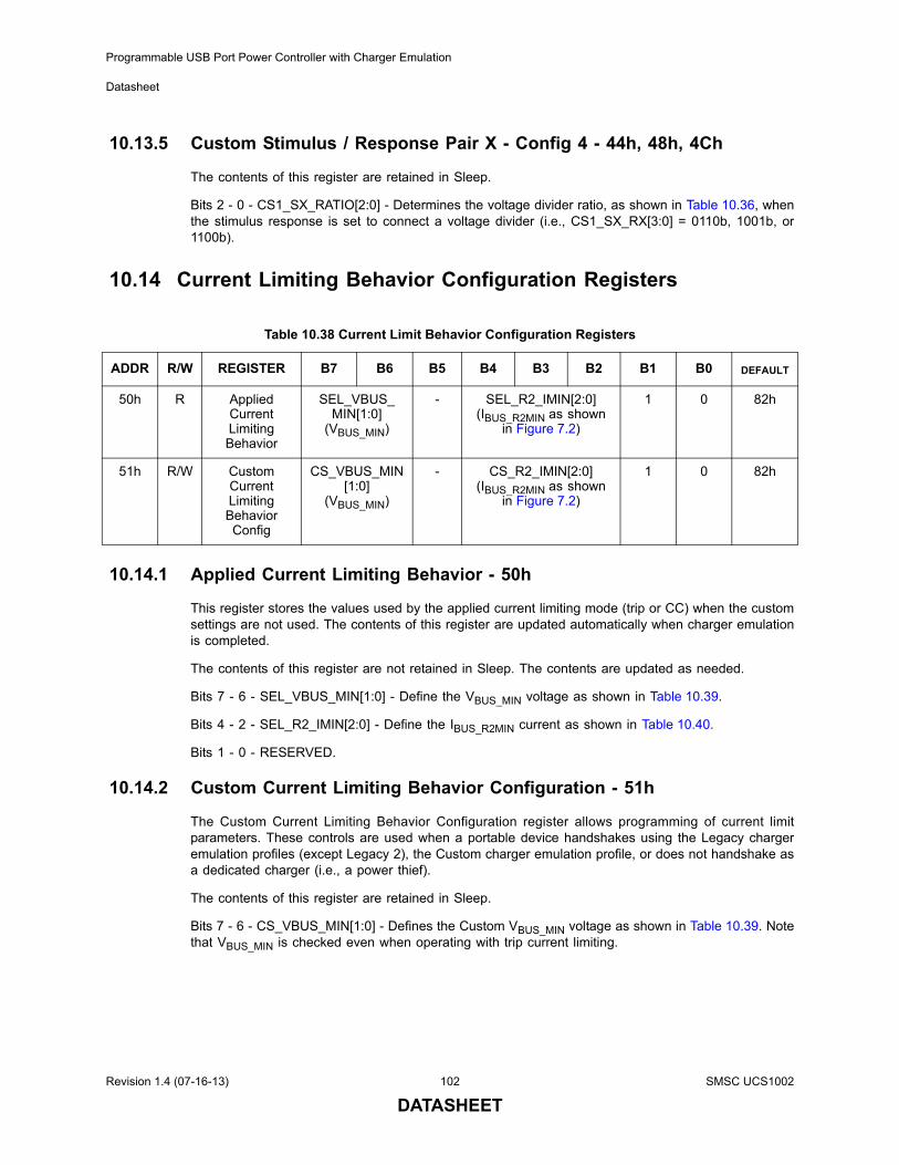
Programmable USB Port Power Controller with Charger Emulation
Datasheet
10.13.5 Custom Stimulus / Response Pair X - Config 4 - 44h, 48h, 4Ch
The contents of this register are retained in Sleep.
Bits 2 - 0 - CS1_SX_RATIO[2:0] - Determines the voltage divider ratio, as shown in Table 10.36, whenthe stimulus response is set to connect a voltage divider (i.e., CS1_SX_RX[3:0] = 0110b, 1001b, or1100b).
10.14 Current Limiting Behavior Configuration Registers
10.14.1 Applied Current Limiting Behavior - 50h
This register stores the values used by the applied current limiting mode (trip or CC) when the customsettings are not used. The contents of this register are updated automatically when charger emulationis completed.
The contents of this register are not retained in Sleep. The contents are updated as needed.
Bits 7 - 6 - SEL_VBUS_MIN[1:0] - Define the VBUS_MIN voltage as shown in Table 10.39.
Bits 4 - 2 - SEL_R2_IMIN[2:0] - Define the IBUS_R2MIN current as shown in Table 10.40.
Bits 1 - 0 - RESERVED.
10.14.2 Custom Current Limiting Behavior Configuration - 51h
The Custom Current Limiting Behavior Configuration register allows programming of current limitparameters. These controls are used when a portable device handshakes using the Legacy chargeremulation profiles (except Legacy 2), the Custom charger emulation profile, or does not handshake asa dedicated charger (i.e., a power thief).
The contents of this register are retained in Sleep.
Bits 7 - 6 - CS_VBUS_MIN[1:0] - Defines the Custom VBUS_MIN voltage as shown in Table 10.39. Notethat VBUS_MIN is checked even when operating with trip current limiting.
Table 10.38 Current Limit Behavior Configuration Registers
ADDR R/W REGISTER B7 B6 B5 B4 B3 B2 B1 B0 DEFAULT
50h R Applied Current Limiting Behavior
SEL_VBUS_ MIN[1:0]
(VBUS_MIN)
- SEL_R2_IMIN[2:0](IBUS_R2MIN as shown
in Figure 7.2)
1 0 82h
51h R/W Custom Current Limiting Behavior Config
CS_VBUS_MIN[1:0]
(VBUS_MIN)
- CS_R2_IMIN[2:0](IBUS_R2MIN as shown
in Figure 7.2)
1 0 82h
Revision 1.4 (07-16-13) 102 SMSC UCS1002
DATASHEET
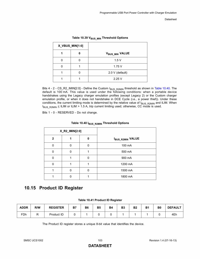
Programmable USB Port Power Controller with Charger Emulation
Datasheet
A
Bits 4 - 2 - CS_R2_IMIN[2:0] - Define the Custom IBUS_R2MIN threshold as shown in Table 10.40. Thedefault is 100 mA. This value is used under the following conditions: when a portable devicehandshakes using the Legacy charger emulation profiles (except Legacy 2) or the Custom chargeremulation profile, or when it does not handshake in DCE Cycle (i.e., a power thief)). Under theseconditions, the current limiting mode is determined by the relative value of IBUS_R2MIN and ILIM. WhenIBUS_R2MIN < ILIM or ILIM > 1.5 A, trip current limiting used; otherwise, CC mode is used.
Bits 1 - 0 - RESERVED - Do not change.
10.15 Product ID Register
The Product ID register stores a unique 8-bit value that identifies the device.
Table 10.39 VBUS_MIN Threshold Options
X_VBUS_MIN[1:0]
VBUS_MIN VALUE1 0
0 0 1.5 V
0 1 1.75 V
1 0 2.0 V (default)
1 1 2.25 V
Table 10.40 IBUS_R2MIN Threshold Options
X_R2_IMIN[2:0]
IBUS_R2MIN VALUE2 1 0
0 0 0 100 mA
0 0 1 500 mA
0 1 0 900 mA
0 1 1 1200 mA
1 0 0 1500 mA
1 0 1 1800 mA
Table 10.41 Product ID Register
DDR R/W REGISTER B7 B6 B5 B4 B3 B2 B1 B0 DEFAULT
FDh R Product ID 0 1 0 0 1 1 1 0 4Eh
SMSC UCS1002 103 Revision 1.4 (07-16-13)
DATASHEET
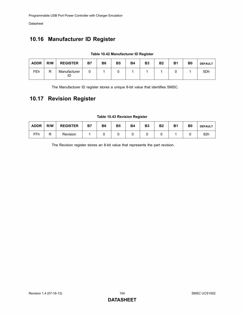
Programmable USB Port Power Controller with Charger Emulation
Datasheet
10.16 Manufacturer ID Register
The Manufacturer ID register stores a unique 8-bit value that identifies SMSC.
10.17 Revision Register
The Revision register stores an 8-bit value that represents the part revision.
Table 10.42 Manufacturer ID Register
ADDR R/W REGISTER B7 B6 B5 B4 B3 B2 B1 B0 DEFAULT
FEh R Manufacturer ID
0 1 0 1 1 1 0 1 5Dh
Table 10.43 Revision Register
ADDR R/W REGISTER B7 B6 B5 B4 B3 B2 B1 B0 DEFAULT
FFh R Revision 1 0 0 0 0 0 1 0 82h
Revision 1.4 (07-16-13) 104 SMSC UCS1002
DATASHEET
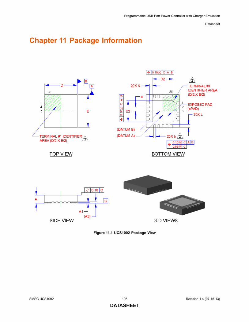
Programmable USB Port Power Controller with Charger Emulation
Datasheet
Chapter 11 Package Information
Figure 11.1 UCS1002 Package View
SMSC UCS1002 105 Revision 1.4 (07-16-13)
DATASHEET
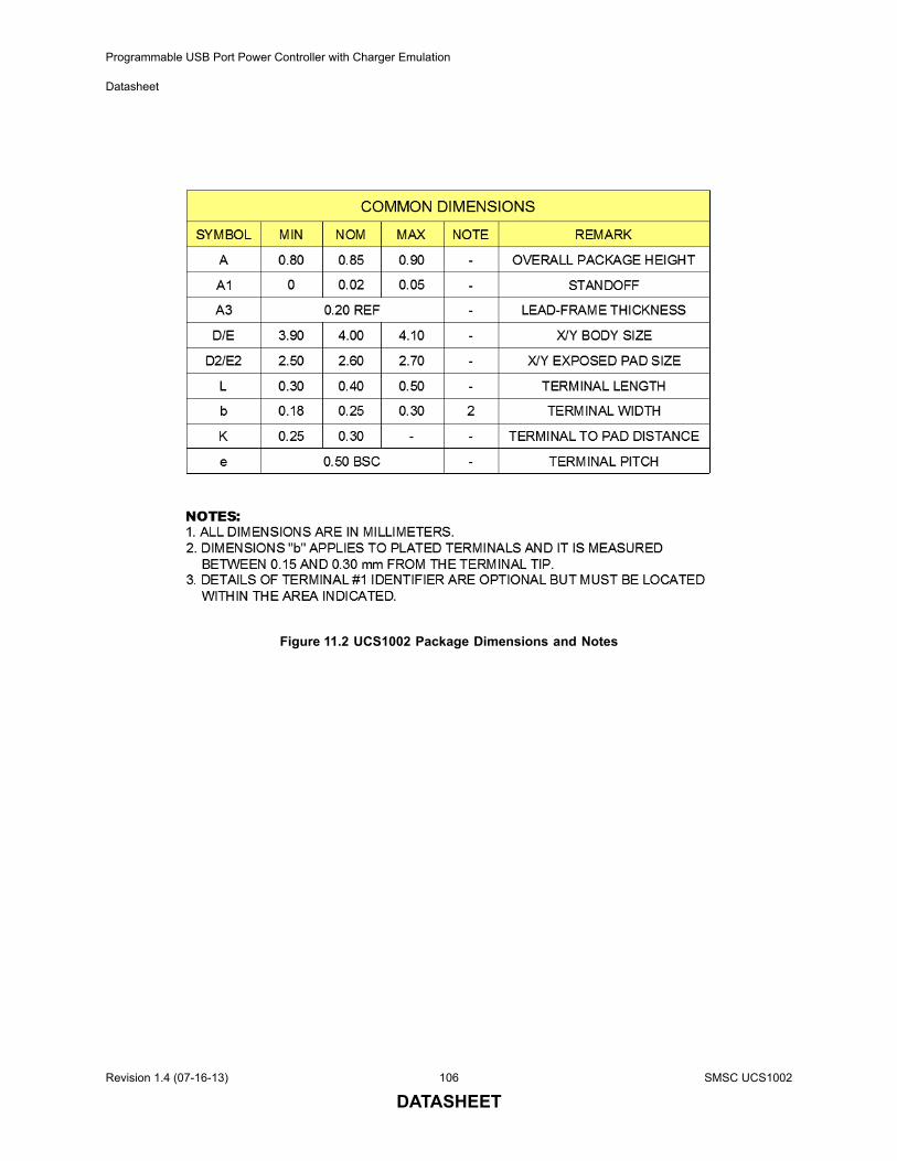
Programmable USB Port Power Controller with Charger Emulation
Datasheet
Figure 11.2 UCS1002 Package Dimensions and Notes
Revision 1.4 (07-16-13) 106 SMSC UCS1002
DATASHEET
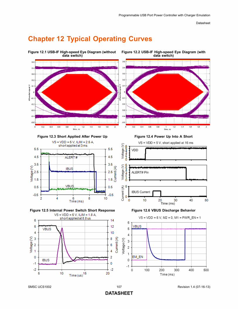
Programmable USB Port Power Controller with Charger Emulation
Datasheet
Chapter 12 Typical Operating Curves
Figure 12.1 USB-IF High-speed Eye Diagram (without data switch)
Figure 12.2 USB-IF High-speed Eye Diagram (with data switch)
Figure 12.3 Short Applied After Power Up Figure 12.4 Power Up Into A Short
Figure 12.5 Internal Power Switch Short Response Figure 12.6 VBUS Discharge Behavior
SMSC UCS1002 107 Revision 1.4 (07-16-13)
DATASHEET
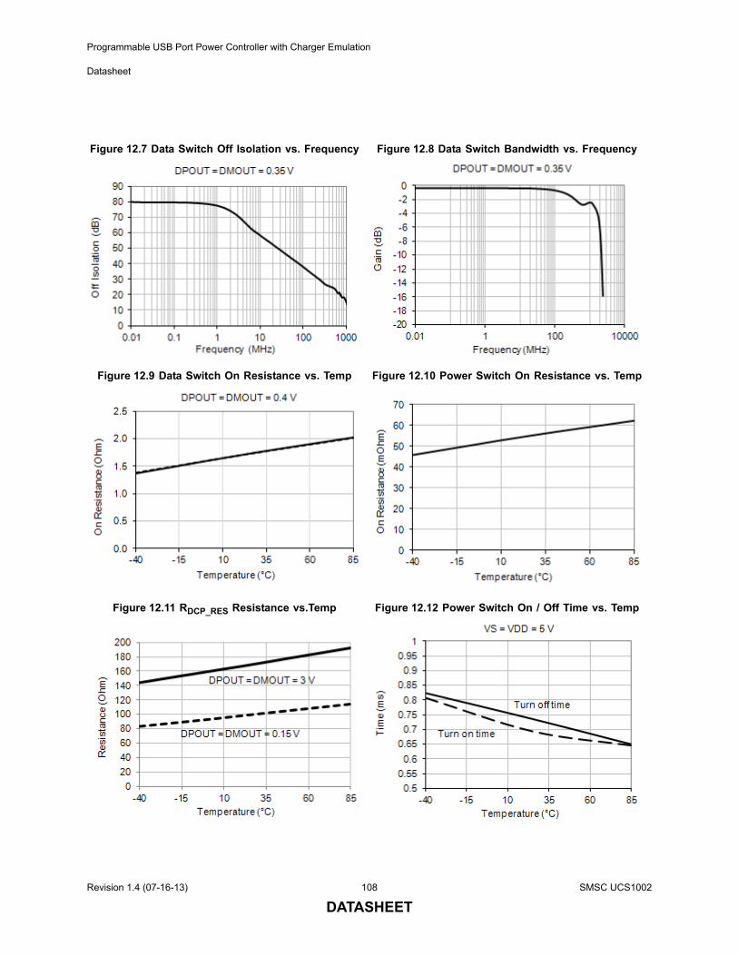
Programmable USB Port Power Controller with Charger Emulation
Datasheet
Figure 12.7 Data Switch Off Isolation vs. Frequency Figure 12.8 Data Switch Bandwidth vs. Frequency
Figure 12.9 Data Switch On Resistance vs. Temp Figure 12.10 Power Switch On Resistance vs. Temp
Figure 12.11 RDCP_RES Resistance vs.Temp Figure 12.12 Power Switch On / Off Time vs. Temp
Revision 1.4 (07-16-13) 108 SMSC UCS1002
DATASHEET
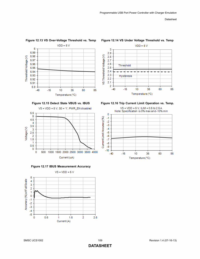
Programmable USB Port Power Controller with Charger Emulation
Datasheet
Figure 12.13 VS Over-Voltage Threshold vs. Temp Figure 12.14 VS Under Voltage Threshold vs. Temp
Figure 12.15 Detect State VBUS vs. IBUS Figure 12.16 Trip Current Limit Operation vs. Temp.
Figure 12.17 IBUS Measurement Accuracy
SMSC UCS1002 109 Revision 1.4 (07-16-13)
DATASHEET
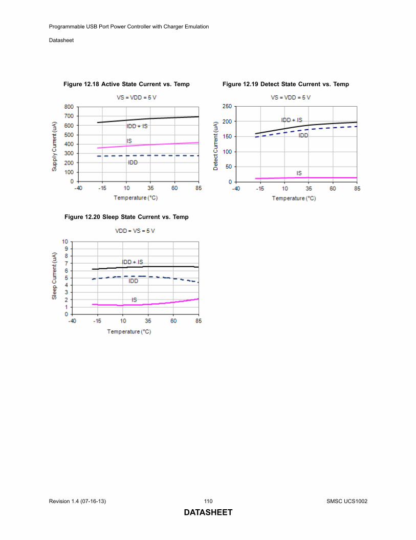
Programmable USB Port Power Controller with Charger Emulation
Datasheet
Figure 12.18 Active State Current vs. Temp Figure 12.19 Detect State Current vs. Temp
Figure 12.20 Sleep State Current vs. Temp
Revision 1.4 (07-16-13) 110 SMSC UCS1002
DATASHEET
Programmable USB Port Power Controller with Charger Emulation
Datasheet
Chapter 13 References
For additional information, the following documents are available from your SMSC representative.
Application Note 24.14 Fundamentals of Custom Charger Emulation
Application Note 24.20 Using the UCS100x or UCS8100x as a Single or Dual Mode Charger
Application Note 25.0 UCS1002 Highest Current Algorithm Using an MCU
Application Note 25.4 UCS1002 Advanced Custom Charging
Application Note 25.5 UCS1002 Smart Battery Charger Hardware Reference Design
Application Note 25.7 UCS1002 Charge Rationing
Application Note 25.16 USB Charging Port ESD Protection Tips for UCS100x
Application Note 26.1 - UCS1002 Current Limit Operation and Features
UCS1002 FAQs (frequently asked questions)
UCS1002-1 Reference Design
UCS1001 / UCS1002 Production Test Method
Charger Test Report
SMSC UCS1002 111 Revision 1.4 (07-16-13)
DATASHEET
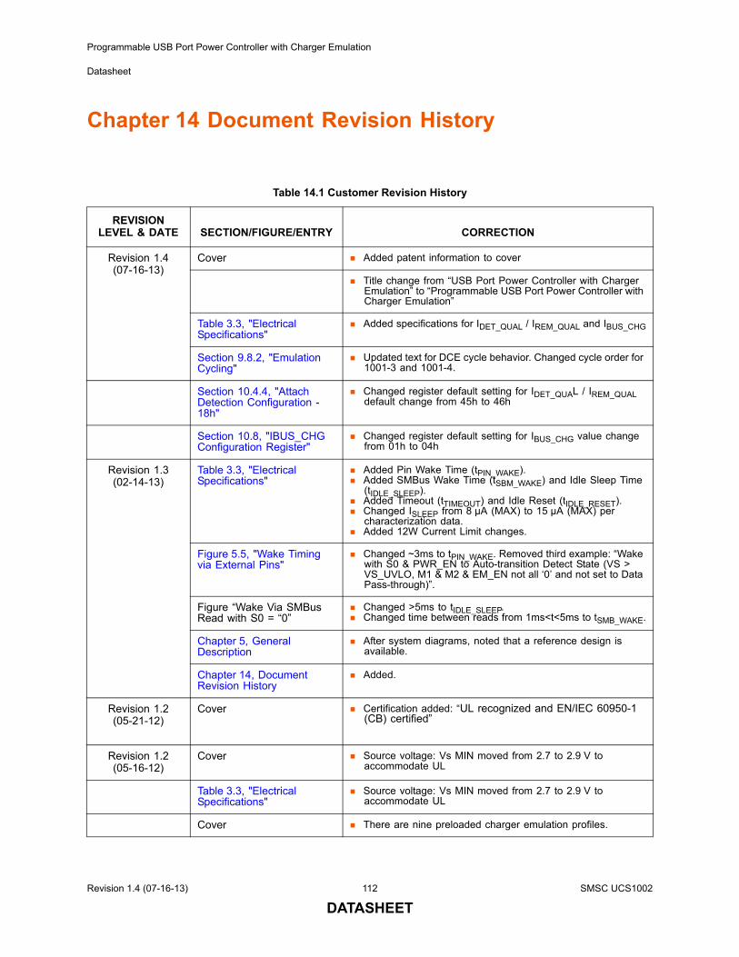
Programmable USB Port Power Controller with Charger Emulation
Datasheet
Chapter 14 Document Revision History
Table 14.1 Customer Revision History
REVISION LEVEL & DATE SECTION/FIGURE/ENTRY CORRECTION
Revision 1.4 (07-16-13)
Cover Added patent information to cover
Title change from “USB Port Power Controller with Charger Emulation” to “Programmable USB Port Power Controller with Charger Emulation”
Table 3.3, "Electrical Specifications"
Added specifications for IDET_QUAL / IREM_QUAL and IBUS_CHG
Section 9.8.2, "Emulation Cycling"
Updated text for DCE cycle behavior. Changed cycle order for 1001-3 and 1001-4.
Section 10.4.4, "Attach Detection Configuration - 18h"
Changed register default setting for IDET_QUAL / IREM_QUAL default change from 45h to 46h
Section 10.8, "IBUS_CHG Configuration Register"
Changed register default setting for IBUS_CHG value change from 01h to 04h
Revision 1.3(02-14-13)
Table 3.3, "Electrical Specifications"
Added Pin Wake Time (tPIN_WAKE). Added SMBus Wake Time (tSBM_WAKE) and Idle Sleep Time
(tIDLE_SLEEP). Added Timeout (tTIMEOUT) and Idle Reset (tIDLE_RESET). Changed ISLEEP from 8 µA (MAX) to 15 µA (MAX) per
characterization data. Added 12W Current Limit changes.
Figure 5.5, "Wake Timing via External Pins"
Changed ~3ms to tPIN_WAKE. Removed third example: “Wake with S0 & PWR_EN to Auto-transition Detect State (VS > VS_UVLO, M1 & M2 & EM_EN not all ‘0’ and not set to Data Pass-through)”.
Figure “Wake Via SMBus Read with S0 = “0”
Changed >5ms to tIDLE_SLEEP. Changed time between reads from 1ms<t<5ms to tSMB_WAKE.
Chapter 5, General Description
After system diagrams, noted that a reference design is available.
Chapter 14, Document Revision History
Added.
Revision 1.2(05-21-12)
Cover Certification added: “UL recognized and EN/IEC 60950-1 (CB) certified”
Revision 1.2(05-16-12)
Cover Source voltage: Vs MIN moved from 2.7 to 2.9 V to accommodate UL
Table 3.3, "Electrical Specifications"
Source voltage: Vs MIN moved from 2.7 to 2.9 V to accommodate UL
Cover There are nine preloaded charger emulation profiles.
Revision 1.4 (07-16-13) 112 SMSC UCS1002
DATASHEET
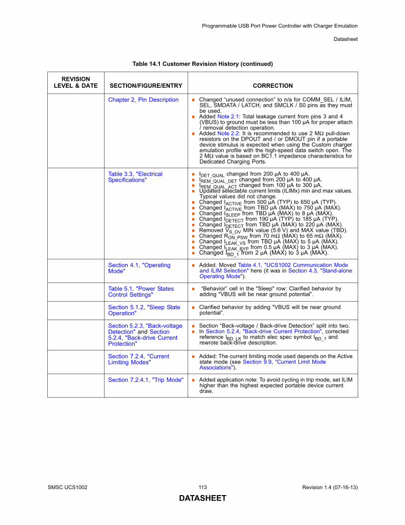
Programmable USB Port Power Controller with Charger Emulation
Datasheet
Chapter 2, Pin Description Changed “unused connection” to n/a for COMM_SEL / ILIM, SEL, SMDATA / LATCH, and SMCLK / S0 pins as they must be used.
Added Note 2.1: Total leakage current from pins 3 and 4 (VBUS) to ground must be less than 100 µA for proper attach / removal detection operation.
Added Note 2.2: It is recommended to use 2 MΩ pull-down resistors on the DPOUT and / or DMOUT pin if a portable device stimulus is expected when using the Custom charger emulation profile with the high-speed data switch open. The 2 MΩ value is based on BC1.1 impedance characteristics for Dedicated Charging Ports.
Table 3.3, "Electrical Specifications"
IDET_QUAL changed from 200 µA to 400 µA. IREM_QUAL_DET changed from 200 µA to 400 µA. IREM_QUAL_ACT changed from 100 µA to 300 µA. Updated selectable current limits (ILIMx) min and max values.
Typical values did not change. Changed IACTIVE from 500 µA (TYP) to 650 µA (TYP). Changed IACTIVE from TBD µA (MAX) to 750 µA (MAX). Changed ISLEEP from TBD µA (MAX) to 8 µA (MAX). Changed IDETECT from 190 µA (TYP) to 185 µA (TYP). Changed IDETECT from TBD µA (MAX) to 220 µA (MAX). Removed VS_OV MIN value (5.6 V) and MAX value (TBD). Changed RON_PSW from 70 mΩ (MAX) to 65 mΩ (MAX). Changed ILEAK_VS from TBD µA (MAX) to 5 µA (MAX). Changed ILEAK_BYP from 0.5 µA (MAX) to 3 µA (MAX). Changed IBD_1 from 2 µA (MAX) to 3 µA (MAX).
Section 4.1, "Operating Mode"
Added. Moved Table 4.1, "UCS1002 Communication Mode and ILIM Selection" here (it was in Section 4.3, "Stand-alone Operating Mode").
Table 5.1, "Power States Control Settings"
“Behavior” cell in the "Sleep" row: Clarified behavior by adding "VBUS will be near ground potential”.
Section 5.1.2, "Sleep State Operation"
Clarified behavior by adding "VBUS will be near ground potential”.
Section 5.2.3, "Back-voltage Detection" and Section 5.2.4, "Back-drive Current Protection"
Section “Back-voltage / Back-drive Detection” split into two. In Section 5.2.4, "Back-drive Current Protection", corrected
reference IBD_LK to match elec spec symbol IBD_1 and rewrote back-drive description.
Section 7.2.4, "Current Limiting Modes"
Added: The current limiting mode used depends on the Active state mode (see Section 9.9, "Current Limit Mode Associations").
Section 7.2.4.1, "Trip Mode" Added application note: To avoid cycling in trip mode, set ILIM higher than the highest expected portable device current draw.
Table 14.1 Customer Revision History (continued)
REVISION LEVEL & DATE SECTION/FIGURE/ENTRY CORRECTION
SMSC UCS1002 113 Revision 1.4 (07-16-13)
DATASHEET
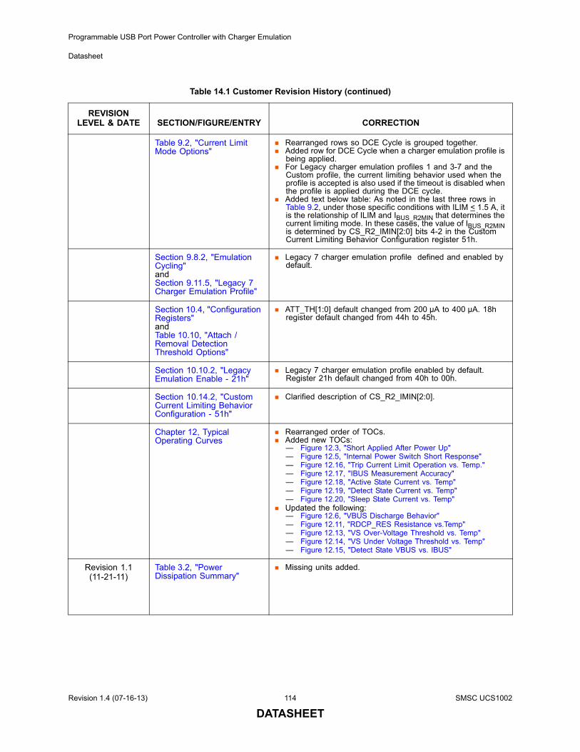
Programmable USB Port Power Controller with Charger Emulation
Datasheet
Table 9.2, "Current Limit Mode Options"
Rearranged rows so DCE Cycle is grouped together. Added row for DCE Cycle when a charger emulation profile is
being applied. For Legacy charger emulation profiles 1 and 3-7 and the
Custom profile, the current limiting behavior used when the profile is accepted is also used if the timeout is disabled when the profile is applied during the DCE cycle.
Added text below table: As noted in the last three rows in Table 9.2, under those specific conditions with ILIM < 1.5 A, it is the relationship of ILIM and IBUS_R2MIN that determines the current limiting mode. In these cases, the value of IBUS_R2MIN is determined by CS_R2_IMIN[2:0] bits 4-2 in the Custom Current Limiting Behavior Configuration register 51h.
Section 9.8.2, "Emulation Cycling"and Section 9.11.5, "Legacy 7 Charger Emulation Profile"
Legacy 7 charger emulation profile defined and enabled by default.
Section 10.4, "Configuration Registers"andTable 10.10, "Attach / Removal Detection Threshold Options"
ATT_TH[1:0] default changed from 200 µA to 400 µA. 18h register default changed from 44h to 45h.
Section 10.10.2, "Legacy Emulation Enable - 21h"
Legacy 7 charger emulation profile enabled by default. Register 21h default changed from 40h to 00h.
Section 10.14.2, "Custom Current Limiting Behavior Configuration - 51h"
Clarified description of CS_R2_IMIN[2:0].
Chapter 12, Typical Operating Curves
Rearranged order of TOCs. Added new TOCs:
— Figure 12.3, "Short Applied After Power Up"— Figure 12.5, "Internal Power Switch Short Response"— Figure 12.16, "Trip Current Limit Operation vs. Temp."— Figure 12.17, "IBUS Measurement Accuracy"— Figure 12.18, "Active State Current vs. Temp"— Figure 12.19, "Detect State Current vs. Temp"— Figure 12.20, "Sleep State Current vs. Temp"
Updated the following:— Figure 12.6, "VBUS Discharge Behavior"— Figure 12.11, "RDCP_RES Resistance vs.Temp"— Figure 12.13, "VS Over-Voltage Threshold vs. Temp"— Figure 12.14, "VS Under Voltage Threshold vs. Temp"— Figure 12.15, "Detect State VBUS vs. IBUS"
Revision 1.1(11-21-11)
Table 3.2, "Power Dissipation Summary"
Missing units added.
Table 14.1 Customer Revision History (continued)
REVISION LEVEL & DATE SECTION/FIGURE/ENTRY CORRECTION
Revision 1.4 (07-16-13) 114 SMSC UCS1002
DATASHEET
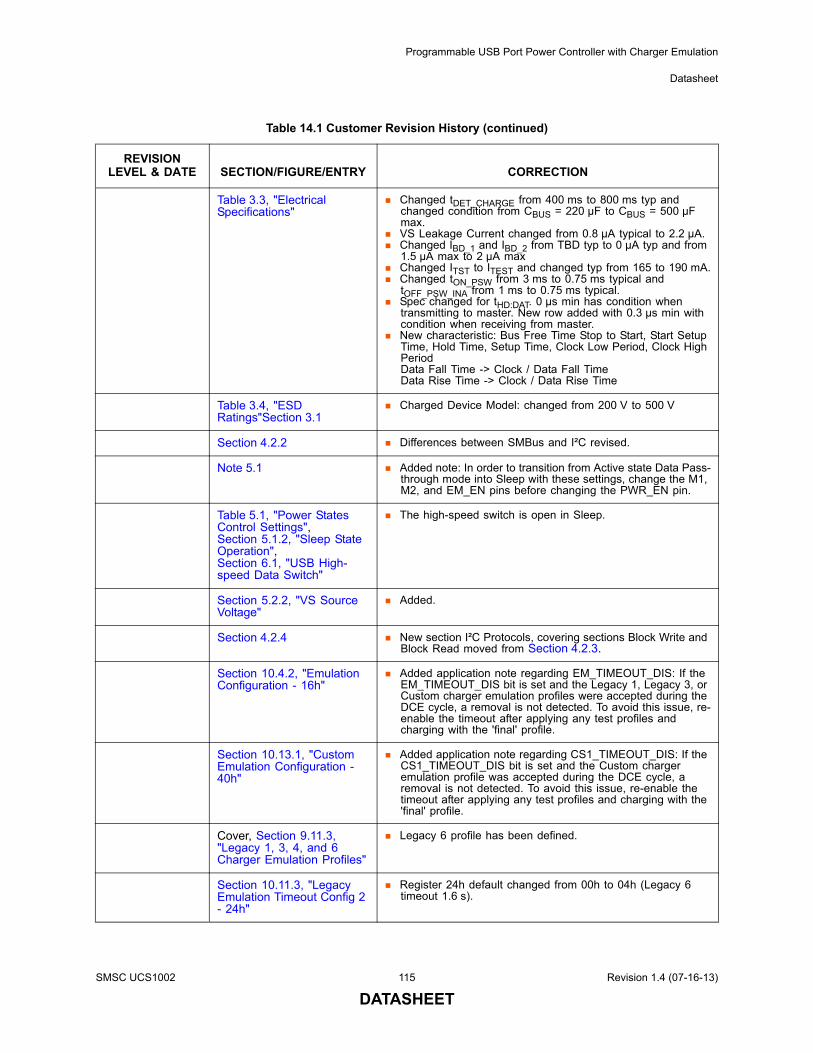
Programmable USB Port Power Controller with Charger Emulation
Datasheet
Table 3.3, "Electrical Specifications"
Changed tDET_CHARGE from 400 ms to 800 ms typ and changed condition from CBUS = 220 µF to CBUS = 500 µF max.
VS Leakage Current changed from 0.8 µA typical to 2.2 µA. Changed IBD_1 and IBD_2 from TBD typ to 0 µA typ and from
1.5 µA max to 2 µA max Changed ITST to ITEST and changed typ from 165 to 190 mA. Changed tON_PSW from 3 ms to 0.75 ms typical and
tOFF_PSW_INA from 1 ms to 0.75 ms typical. Spec changed for tHD:DAT. 0 µs min has condition when
transmitting to master. New row added with 0.3 µs min with condition when receiving from master.
New characteristic: Bus Free Time Stop to Start, Start Setup Time, Hold Time, Setup Time, Clock Low Period, Clock High Period Data Fall Time -> Clock / Data Fall TimeData Rise Time -> Clock / Data Rise Time
Table 3.4, "ESD Ratings"Section 3.1
Charged Device Model: changed from 200 V to 500 V
Section 4.2.2 Differences between SMBus and I²C revised.
Note 5.1 Added note: In order to transition from Active state Data Pass-through mode into Sleep with these settings, change the M1, M2, and EM_EN pins before changing the PWR_EN pin.
Table 5.1, "Power States Control Settings",Section 5.1.2, "Sleep State Operation",Section 6.1, "USB High-speed Data Switch"
The high-speed switch is open in Sleep.
Section 5.2.2, "VS Source Voltage"
Added.
Section 4.2.4 New section I²C Protocols, covering sections Block Write and Block Read moved from Section 4.2.3.
Section 10.4.2, "Emulation Configuration - 16h"
Added application note regarding EM_TIMEOUT_DIS: If the EM_TIMEOUT_DIS bit is set and the Legacy 1, Legacy 3, or Custom charger emulation profiles were accepted during the DCE cycle, a removal is not detected. To avoid this issue, re-enable the timeout after applying any test profiles and charging with the 'final' profile.
Section 10.13.1, "Custom Emulation Configuration - 40h"
Added application note regarding CS1_TIMEOUT_DIS: If the CS1_TIMEOUT_DIS bit is set and the Custom charger emulation profile was accepted during the DCE cycle, a removal is not detected. To avoid this issue, re-enable the timeout after applying any test profiles and charging with the 'final' profile.
Cover, Section 9.11.3, "Legacy 1, 3, 4, and 6 Charger Emulation Profiles"
Legacy 6 profile has been defined.
Section 10.11.3, "Legacy Emulation Timeout Config 2 - 24h"
Register 24h default changed from 00h to 04h (Legacy 6 timeout 1.6 s).
Table 14.1 Customer Revision History (continued)
REVISION LEVEL & DATE SECTION/FIGURE/ENTRY CORRECTION
SMSC UCS1002 115 Revision 1.4 (07-16-13)
DATASHEET
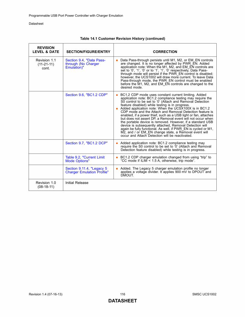
Programmable USB Port Power Controller with Charger Emulation
Datasheet
Revision 1.1(11-21-11)
cont.
Section 9.4, "Data Pass-through (No Charger Emulation)"
Data Pass-through persists until M1, M2, or EM_EN controls are changed. It is no longer affected by PWR_EN. Added application note: When the M1, M2, and EM_EN controls are set to ‘0’, ‘1’, ‘0’ or to ‘1’, ‘1’, ‘0’ respectively, Data Pass-through mode will persist if the PWR_EN control is disabled; however, the UCS1002 will draw more current. To leave Data Pass-through mode, the PWR_EN control must be enabled before the M1, M2, and EM_EN controls are changed to the desired mode.
Section 9.6, "BC1.2 CDP" BC1.2 CDP mode uses constant current limiting. Added application note: BC1.2 compliance testing may require the S0 control to be set to ‘0’ (Attach and Removal Detection feature disabled) while testing is in progress.
Added application note: When the UCSX100X is in BC1.2 CDP mode and the Attach and Removal Detection feature is enabled, if a power thief, such as a USB light or fan, attaches but does not assert DP, a Removal event will not occur when the portable device is removed. However, if a standard USB device is subsequently attached, Removal Detection will again be fully functional. As well, if PWR_EN is cycled or M1, M2, and / or EM_EN change state, a Removal event will occur and Attach Detection will be reactivated.
Section 9.7, "BC1.2 DCP" Added application note: BC1.2 compliance testing may require the S0 control to be set to ‘0’ (Attach and Removal Detection feature disabled) while testing is in progress.
Table 9.2, "Current Limit Mode Options"
BC1.2 CDP charger emulation changed from using “trip” to “CC mode if ILIM < 1.5 A, otherwise, trip mode”.
Section 9.11.4, "Legacy 5 Charger Emulation Profile"
Added. The Legacy 5 charger emulation profile no longer applies a voltage divider. It applies 900 mV to DPOUT and DMOUT.
Revision 1.0(08-18-11)
Initial Release
Table 14.1 Customer Revision History (continued)
REVISION LEVEL & DATE SECTION/FIGURE/ENTRY CORRECTION
Revision 1.4 (07-16-13) 116 SMSC UCS1002
DATASHEET