Embed Size (px)
Citation preview
UFS 3.0Controller Design Considerations
JEDEC Mobile & IOT Forum
Copyright © 2018Phison Electronics Corp.Keith Tsai
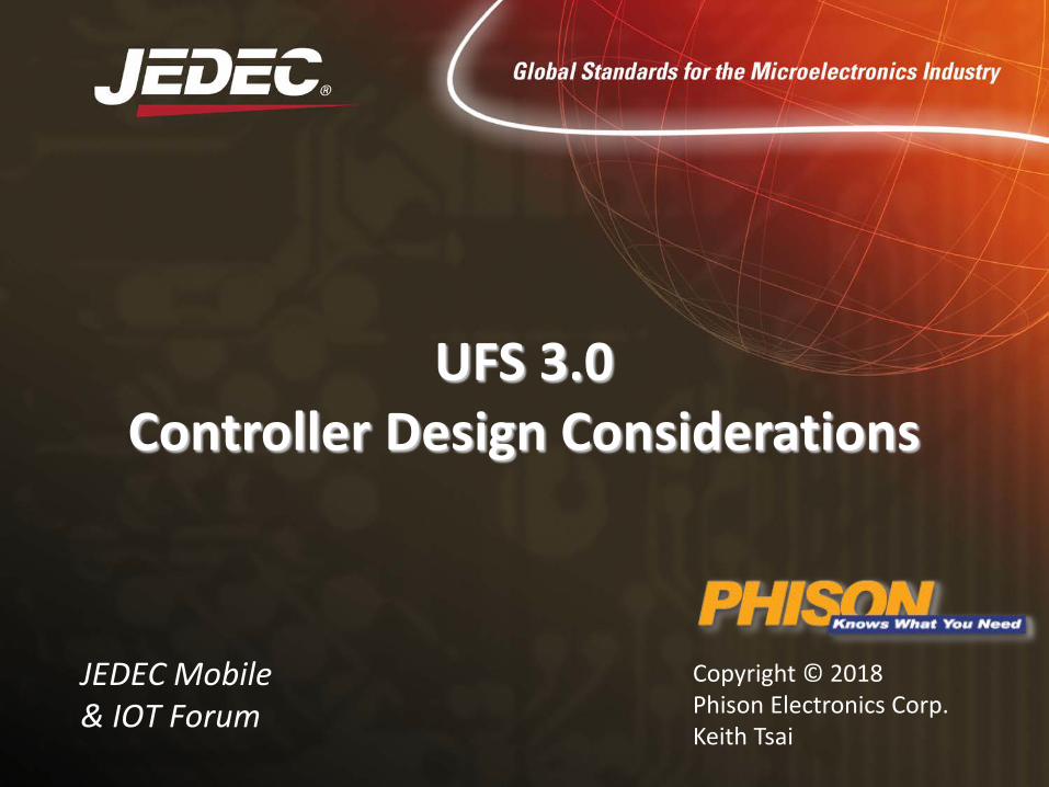
Mobile Storage Evolution
eMMC• Latest widely adopted standard before UFS 2.x• Limited to 400MB/s (duplex) since 2013
UFS 1.x• Not adopted
UFS 2.x• Offers desktop-grade performance of ~1200MB/s over full-duplex links• Good adoption in flagship devices (2017)
UFS 3.0• Doubles UFS 2.x performance, offering ~2400MB/s• Requirements are tough for mobile form factors
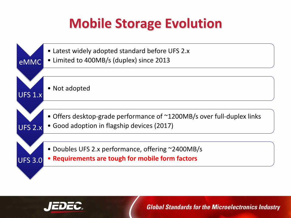
Automotive UFSAEC-Q100ISO-26262ISO-16949
CommercialUFS and uMCP
CommercialUFS Card
Performance Low-Mid High Low (1-Lane only)
Density Application-Specific Mid/High Mid/High
Cost Higher Optimized Lower
Reliability High Standard Standard
Support Long term Standard Standard
Application - Infotainment- ADAS
- Smartphone- Tablet- Chromebook- Slim laptops
- Camera (4K, 8K...)- Smartphone- Tablet- Chromebook- Slim laptops
UFS 3.0
Market Segmentation
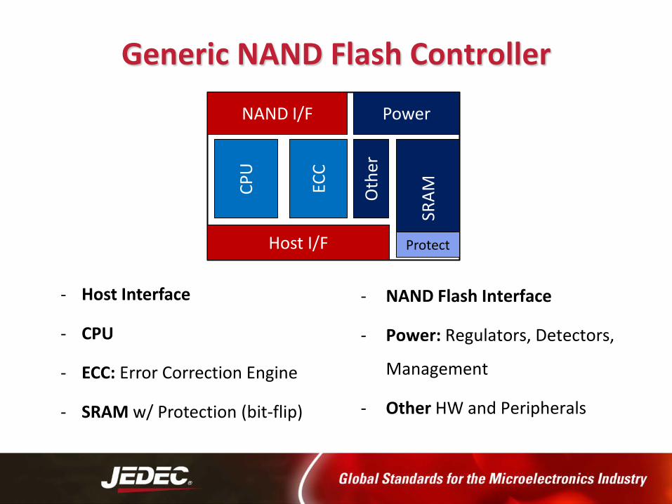
- NAND Flash Interface
- Power: Regulators, Detectors,
Management
- Other HW and Peripherals
Host I/F
NAND I/F Power
ECC
SRAMCP
U
Oth
er
Protect
- Host Interface
- CPU
- ECC: Error Correction Engine
- SRAM w/ Protection (bit-flip)
Generic NAND Flash Controller
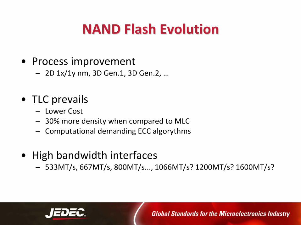
• Process improvement– 2D 1x/1y nm, 3D Gen.1, 3D Gen.2, …
• TLC prevails– Lower Cost– 30% more density when compared to MLC– Computational demanding ECC algorythms
• High bandwidth interfaces– 533MT/s, 667MT/s, 800MT/s..., 1066MT/s? 1200MT/s? 1600MT/s?
NAND Flash Evolution
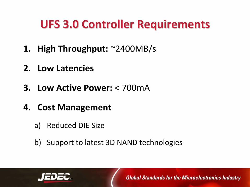
1. High Throughput: ~2400MB/s
2. Low Latencies
3. Low Active Power: < 700mA
4. Cost Management
a) Reduced DIE Size
b) Support to latest 3D NAND technologies
UFS 3.0 Controller Requirements
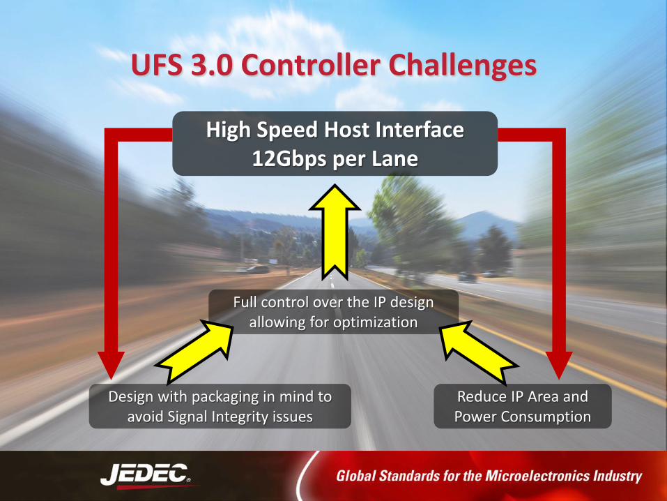
Full control over the IP design allowing for optimization
Design with packaging in mind to avoid Signal Integrity issues
Reduce IP Area and Power Consumption
High Speed Host Interface12Gbps per Lane
UFS 3.0 Controller Challenges
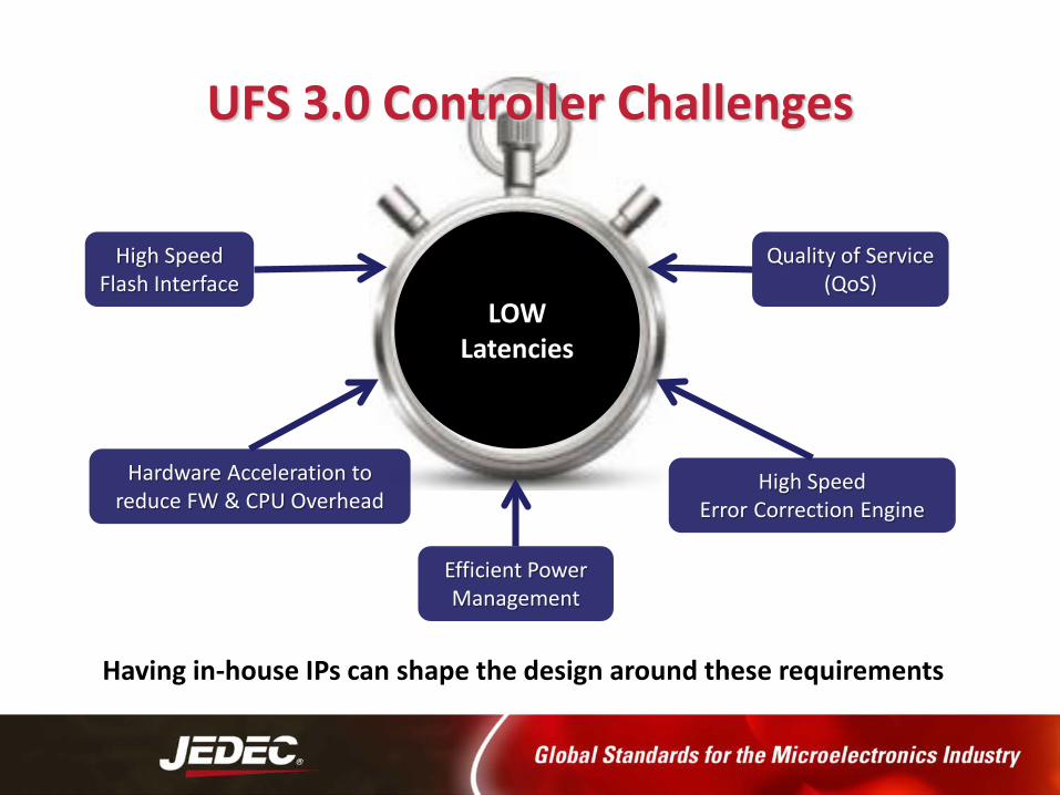
High SpeedError Correction Engine
Hardware Acceleration to reduce FW & CPU Overhead
High SpeedFlash Interface
Quality of Service(QoS)
LOWLatencies
Efficient Power Management
UFS 3.0 Controller Challenges
Having in-house IPs can shape the design around these requirements
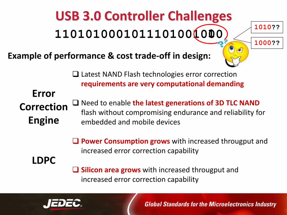
Error Correction
Engine
LDPC
Latest NAND Flash technologies error correction requirements are very computational demanding
Need to enable the latest generations of 3D TLC NANDflash without compromising endurance and reliability for embedded and mobile devices
Power Consumption grows with increased througput and increased error correction capability
Silicon area grows with increased througput and increased error correction capability
Example of performance & cost trade-off in design:
110101000101110100100011010??
1000??
USB 3.0 Controller Challenges

Wafer Cost
ProductionSchedule
Power Consumption
DIE AreaReduction
Newer Process: All About the Right Balance
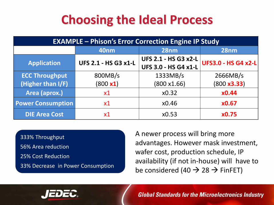
EXAMPLE – Phison’s Error Correction Engine IP Study40nm 28nm 28nm
Application UFS 2.1 - HS G3 x1-L UFS 2.1 - HS G3 x2-LUFS 3.0 - HS G4 x1-L UFS3.0 - HS G4 x2-L
ECC Throughput (Higher than I/F)
800MB/s(800 x1)
1333MB/s(800 x1.66)
2666MB/s(800 x3.33)
Area (aprox.) x1 x0.32 x0.44Power Consumption x1 x0.46 x0.67
DIE Area Cost x1 x0.53 x0.75
333% Throughput56% Area reduction25% Cost Reduction33% Decrease in Power Consumption
A newer process will bring more advantages. However mask investment, wafer cost, production schedule, IP availability (if not in-house) will have to be considered (40 28 FinFET)
Choosing the Ideal Process
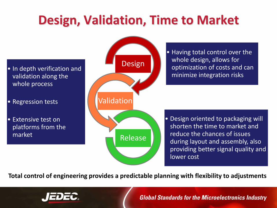
• Having total control over the whole design, allows for optimization of costs and can minimize integration risks
Design• In depth verification and
validation along the whole process
• Regression tests
• Extensive test on platforms from the market
Validation
• Design oriented to packaging will shorten the time to market and reduce the chances of issues during layout and assembly, also providing better signal quality and lower cost
Release
Design, Validation, Time to Market
Total control of engineering provides a predictable planning with flexibility to adjustments
UFS 3.0 performance is comparable to NVMe SSD, yet power and
cost are expected to be similar to eMMC: meeting the dynamic
mobile market requirements
In device controller design, the balance between performance,
power and cost is critical. In addition, a total control of the design
will offer more flexibility to optimize the solution
Validation strategy, NAND support & time to market are the
determinants of a successful product
Summary

Thank You


![Product Data Sheet - seoulsemicon.com Y22P_Rev1.0_171… · Luminous Efficacy [lm/W] @700mA Part Number 700mA 1000mA 1500mA 70 6500 299 310 422 586 159 S1W0-2222657003-00000000 …](https://img.pdfslide.net/doc/110x75/5b156f947f8b9a1a398c605c/product-data-sheet-y22prev10171-luminous-efficacy-lmw-700ma-part-number.jpg)