Embed Size (px)
Citation preview
Ultra-compact silicon nitride grating coupler for microscopy systems
YUNPENG ZHU,1,2,* JIE WANG,1,2 WEIQIANG XIE,1,2 BIN TIAN,1,2 YANLU LI,1,2
EDOUARD BRAINIS,2,3 YUQING JIAO,4 AND DRIES VAN THOURHOUT1,2
1Photonics Research Group, Department of Information Technology (INTEC), Ghent University, 9052 Ghent, Belgium 2Center of Nano and Biophotonics (NB Photonics), Ghent Univerisity, Ghent B-9000, Belgium 3Physics and Chemistry of Nanostructures, Ghent University, Krijgslaan 281-S3, 9000 Ghent, Belgium 4Institute for Photonic Integration (IPI), Eindhoven University of Technology, Eindhoven 5600MB, The Netherlands *[email protected]
Abstract: Grating couplers have been widely used for coupling light between photonic chips and optical fibers. For various quantum-optics and bio-optics experiments, on the other hand, there is a need to achieve good light coupling between photonic chips and microscopy systems. Here, we propose an ultra-compact silicon nitride (SiN) grating coupler optimized for coupling light from a waveguide to a microscopy system. The grating coupler is about 4 by 2 μm2 in size and a 116 nm 1 dB bandwidth can be achieved theoretically. An optimized fabrication process was developed to realize suspended SiN waveguides integrated with these couplers on top of a highly reflective bottom mirror. Experimental results show that up to 53% (2.76 dB loss) of the power of the TE mode can be coupled from a suspended SiN waveguide to a microscopy system with a numerical aperture (NA) = 0.65. Simulations show this efficiency can increase up to 75% (1.25 dB loss) for NA = 0.95. © 2017 Optical Society of America under the terms of the OSA Open Access Publishing Agreement
OCIS codes: (130.3120) Integrated optics devices; (050.1950) Diffraction gratings.
References and links
1. D. Taillaert, W. Bogaerts, P. Bienstman, T. F. Krauss, P. Van Daele, I. Moerman, S. Verstuyft, K. De Mesel, and R. Baets, “An out-of-plane grating coupler for efficient butt-coupling between compact planar waveguides and single-mode fibers,” IEEE J. Quantum Electron. 38(7), 949–955 (2002).
2. D. Taillaert, P. Bienstman, and R. Baets, “Compact efficient broadband grating coupler for silicon-on-insulator waveguides,” Opt. Lett. 29(23), 2749–2751 (2004).
3. A. Mekis, S. Gloeckner, G. Masini, A. Narasimha, T. Pinguet, S. Sahni, and P. De Dobbelaere, “A grating-coupler-enabled CMOS photonics platform,” IEEE J. Sel. Top. Quantum Electron. 17(3), 597–608 (2011).
4. G. Roelkens, D. Van Thourhout, and R. Baets, “High efficiency Silicon-on-Insulator grating coupler based on a poly-Silicon overlay,” Opt. Express 14(24), 11622–11630 (2006).
5. A. Z. Subramanian, S. Selvaraja, P. Verheyen, A. Dhakal, K. Komorowska, and R. Baets, “Near-infrared grating couplers for silicon nitride photonic wires,” IEEE Photonics Technol. Lett. 24(19), 1700–1703 (2012).
6. W. C. Lai, S. Chakravarty, Y. Zou, and R. T. Chen, “Silicon nano-membrane based photonic crystal microcavities for high sensitivity bio-sensing,” Opt. Lett. 37(7), 1208–1210 (2012).
7. A. Nitkowski, L. Chen, and M. Lipson, “Cavity-enhanced on-chip absorption spectroscopy using microring resonators,” Opt. Express 16(16), 11930–11936 (2008).
8. A. Politi, M. J. Cryan, J. G. Rarity, S. Yu, and J. L. O’Brien, “Silica-on-silicon waveguide quantum circuits,” Science 320(5876), 646–649 (2008).
9. A. Imamog, D. D. Awschalom, G. Burkard, D. P. DiVincenzo, D. Loss, M. Sherwin, and A. Small, “Quantum information processing using quantum dot spins and cavity QED,” Phys. Rev. Lett. 83(20), 4204–4207 (1999).
10. J. Wang, S. Paesani, R. Santagati, S. Knauer, A. A. Gentile, N. Wiebe, M. Petruzzella, J. L. O’Brien, J. G. Rarity, A. Laing, and M. G. Thompson, “Experimental quantum Hamiltonian learning,” Nat. Phys. 13(6), 551–555 (2017).
11. D. Bouwmeester, J. Pan, K. Mattle, M. Eibl, H. Weinfurter, and A. Zeilinger, “Experimental quantum teleportation,” Nature 390(6660), 575–579 (1997).
12. E. Knill, R. Laflamme, and G. J. Milburn, “A scheme for efficient quantum computation with linear optics,” Nature 409(6816), 46–52 (2001).
13. M. A. Nielsen and I. L. Chuang, Quantum Computation and Quantum Information (Cambridge University, Cambridge, 2000).
Vol. 25, No. 26 | 25 Dec 2017 | OPTICS EXPRESS 33297
#309058 Journal © 2017
https://doi.org/10.1364/OE.25.033297 Received 12 Oct 2017; revised 9 Dec 2017; accepted 12 Dec 2017; published 21 Dec 2017
14. J. W. Silverstone, D. Bonneau, K. Ohira, N. Suzuki, H. Yoshida, N. Iizuka, M. Ezaki, C. M. Natarajan, M. G. Tanner, R. H. Hadfield, V. Zwiller, G. D. Marshall, J. G. Rarity, J. L. O’Brien, and M. G. Thompson, “On-chip quantum interference between silicon photon-pair sources,” Nat. Photonics 8(2), 104–108 (2014).
15. C. P. Dietrich, A. Fiore, M. G. Thompson, M. Kamp, and S. Höfling, “GaAs integrated quantum photonics: Towards compact and multi-functional quantum photonic integrated circuits,” Laser Photonics Rev. 10, 870 (2016).
16. P. Michler, A. Imamoglu, M. D. Mason, P. J. Carson, G. F. Strouse, and S. K. Buratto, “Quantum correlation among photons from a single quantum dot at room temperature,” Nature 406(6799), 968–970 (2000).
17. X. Brokmann, G. Messin, P. Desbiolles, E. Giacobino, M. Dahan, and J. P. Hermier, “Colloidal CdSe/ZnS quantum dots as single-photon sources,” New J. Phys. 6(1), 99 (2004).
18. W. Xie, Y. Zhu, T. Aubert, S. Verstuyft, Z. Hens, and D. Van Thourhout, “Low-loss silicon nitride waveguide hybridly integrated with colloidal quantum dots,” Opt. Express 23(9), 12152–12160 (2015).
19. S. Bisschop, A. Guille, D. Van Thourhout, Z. Hens, and E. Brainis, “Broadband enhancement of single photon emission and polarization dependent coupling in silicon nitride waveguides,” Opt. Express 23(11), 13713–13724 (2015).
20. W. Xie, R. Gomes, T. Aubert, S. Bisschop, Y. Zhu, Z. Hens, E. Brainis, and D. Van Thourhout, “Nanoscale and Single-Dot Patterning of Colloidal Quantum Dots,” Nano Lett. 15(11), 7481–7487 (2015).
21. A. Faraon, I. Fushman, D. Englund, N. Stoltz, P. Petroff, and J. Vucković, “Dipole induced transparency in waveguide coupled photonic crystal cavities,” Opt. Express 16(16), 12154–12162 (2008).
22. I. J. Luxmoore, N. A. Wasley, A. J. Ramsay, A. C. T. Thijssen, R. Oulton, M. Hugues, S. Kasture, V. G. Achanta, A. M. Fox, and M. S. Skolnick, “Interfacing spins in an InGaAs quantum dot to a semiconductor waveguide circuit using emitted photons,” Phys. Rev. Lett. 110(3), 037402 (2013).
23. W. Shimizu, N. Nagai, K. Kohno, K. Hirakawa, and M. Nomura, “Waveguide coupled air-slot photonic crystal nanocavity for optomechanics,” Opt. Express 21(19), 21961–21969 (2013).
24. J. Sun, E. Timurdogan, A. Yaacobi, E. S. Hosseini, and M. R. Watts, “Large-scale nanophotonic phased array,” Nature 493(7431), 195–199 (2013).
25. A. Rahim, E. Ryckeboer, A. Z. Subramanian, S. Clemmen, B. Kuyken, A. Dhakal, A. Raza, A. Hermans, M. Muneeb, S. Dhoore, Y. Li, U. Dave, P. Bienstman, N. Le Thomas, G. Roelkens, D. Van Thourhout, P. Helin, S. Severi, X. Rottenberg, and R. Baets, “Expanding the Silicon Photonics Portfolio With Silicon Nitride Photonic Integrated Circuits,” J. Lightwave Technol. 35(4), 639–649 (2017).
1. Introduction
Grating couplers are now extensively used to couple light between optical fibers and photonic integrated circuits (PICs). The use of grating couplers allows avoiding expensive processing and packaging steps such as facet polishing and lensed fiber alignment. Grating couplers with high efficiency and relatively large optical bandwidth [1–4] have been successfully demonstrated for traditional telecom wavelength and near infrared wavelengths [5]. They have become standard components in PIC platforms and enable wafer scale testing.
PICs, originally developed mainly for telecom applications, are now also finding widespread application in domains as diverse as bio-sensing [6], spectroscopy [7] and quantum optics [8,9]. Compared to early experimental demonstrations of quantum optics networks, which typically relied on bulky optical components, a PIC platform provides improved thermal and mechanical stability and scalability [10]. A key building block thereby is an integrated single photon source, required in applications as diverse as quantum teleportation [11], quantum computation [12] and several schemes for quantum cryptography [13]. Current efforts to realize integrated single photon sources rely, amongst others, on using nonlinear four-wave mixing [14] and epitaxially grown quantum dots [15]. Also colloidal CdSe/ZnS core-shell quantum dots (QD) have been shown to be efficient single-photon emitters [16,17]. Further, we recently have demonstrated a hybrid QD-SiN platform, which allows to combine colloidal quantum dots with low loss waveguides [18]. Moreover in [19] we showed that a dipole emitter embedded in a SiN waveguide with optimized dimensions can couple up to 43% of its emission to a single waveguide mode, with a 95% polarization ratio. Finally, we experimentally demonstrated the capability for positioning individual quantum dots at a predefined location with high yield [20]. The combination of these results shows the hybrid QD-SiN platform offers the potential for realizing efficient on chip single photon sources in combination with complex photonic circuits. However, to characterize these QDs based integrated single photon sources and the associated photonic circuits, it is desired to use a high numerical aperture (NA) microscopy system, since it can help to
Vol. 25, No. 26 | 25 Dec 2017 | OPTICS EXPRESS 33298
accurately localize the optical excitation and maximize the collection efficiency. An important building block for such systems is an efficient, compact and broad band coupler that can extract the light from the PIC towards a standard microscopy system. Standard grating couplers, which are optimized for fiber-to-chip coupling, typically not only have dimensions similar to those of the core of single mode optical fibers (100 µm2) but also need an optimized taper between the waveguide and the grating coupler to achieve high coupling efficiency. Therefore, they are usually not compact enough for large NA microscopy applications. On the other hand, single mode optical fibers have a small numerical aperture (NA) compared to a typical microscopy system. The much larger NA of a microscopy system allows a wider collection angle, possibly leading to higher coupling efficiency and wider bandwidth. Hence there is a need for compact, efficient and broad-band components, which can couple light from a chip to an objective. There has been some work describing compact on-chip couplers before [21–23]. A similar design has also been used as an optical antenna unit in a nanophotonic phased array, to couple light from a waveguide to free space, focusing on beam steering applications [24]. However, these designs are based on silicon or III-V PICs, which exhibit a higher index contrast. Compared with the silicon and III-V PIC platforms, the SiN PIC platform offers a wider optical transparent window with lower optical propagation loss [25]. However, its lower index contrast makes realizing efficient grating couplers more challenging. Therefore, in this paper, we present a methodological approach for the design, fabrication and characterization of an ultra-compact silicon nitride (SiN) grating for coupling light from a PIC waveguide to a microscopy system.
2. Grating coupler design
As shown in Fig. 1(a), the parameters of a diffraction grating that can be optimized are usually its period, the etching depth, the filling factor, the number of periods and the distance between grating and substrate. All simulations were carried out at the He-Ne laser’s lasing wavelength of 632.8 nm. This wavelength lies in the range of our colloidal QDs emission bandwidth and it allows for straightforward experimental verification of the simulation results. We choose silicon nitride (n = 1.91@ 632.8 nm) as the waveguide material and fixed the thickness of the waveguide to 220 nm. In previous work, simulations showed that this waveguide thickness optimizes light coupling between emission from an embedded QD emitter to the waveguide optical mode [19]. The top view of the proposed grating coupler is shown in Fig. 1(b). The grating coupler has been designed in a circular shape. We are aiming to under etch the substrate material beneath the grating, on the one hand because it enhances the coupling of the emission of an embedded dipole emitter to the waveguide optical mode, while on the other hand it further enhances the efficiency of the grating coupler. Therefore, a small supporting beam has been added between the grating coupler and the waveguide to ensure a fully suspended structure is realistic.
We choose to etch completely through the grating to increase its contrast while in the meantime also making the fabrication process easier. The filling factor is fixed to 0.5 to guarantee an easier process. To determine the best parameters for the grating coupler, 3D finite difference time domain (FDTD) simulations were carried out. The fundamental TE mode of the suspended waveguide (600 nm in width, 220 nm in thickness) has been used to excite the grating. A field and power monitor have been placed 0.5 μm above the grating to check the power scattered upwards by the grating coupler. Since we are more interested in how much light will be captured by an objective, also the far field radiation pattern of this field and power monitor has been simulated, to be able to calculate the power collected by an objective with a given NA (0.65 in the remainder of this paper).
Vol. 25, No. 26 | 25 Dec 2017 | OPTICS EXPRESS 33299

Fig. 1. (a) The schematic of the grating coupler design, in this paper the grating is completely etch through to enhance the contrast; (b) The top view of the proposed circular shape grating coupler, a small supporting beam is added between the grating coupler and the waveguide to ensure a fully suspended structure realistic.
We first varied the period of a grating coupler consisting of only 3 periods without substrate. Note that the supporting beam is considered in the simulation. We calculated the total power coupled upwards and the far field as collected by an objective with NA = 0.65. The results are shown in Fig. 2(a). The maximum upwards coupling for in the range 600 nm to 700 nm corresponds to the situation whereby both the first order and the second order diffraction are at least partly picked up by the objective. The dip around 525 nm corresponds to the period for which the first order diffraction is radiated nearly vertically and the second order diffraction is coupled backwards in the waveguide, leading to reduced upwards coupling. In this figure we also find a reduced upwards diffraction for periods around 800 nm and 1050 nm, corresponding to the situations whereby the third and fourth order diffraction are coupled in the waveguide. Also note that the N.A. 0.65 collection efficiency decreases dramatically with increasing period, which can be attributed to the fact that more light goes outside of the collection angle for larger grating periods (more light is coupled in higher order diffraction angle with large inclination).
As we aim to minimize the grating coupler size, we also simulated the influence of the number of periods. Figure 2(b) shows the power coupled upwards and the power collected within an NA = 0.65 as function of the number of periods, with the period of the grating fixed to 600 nm. The results clearly show that with an increased number of periods, more light gets deflected upwards. Fully etching the grating ensured a high contrast and results in an efficient diffraction for the light from the waveguide. From the simulation, we can conclude that 3 periods form a good balance between the coupling efficiency and the compactness of the grating coupler.
Fig. 2. (a) 3D FDTD simulation results of period length vs power up/power collected with NA = 0.65; (b)3D FDTD simulation results of number of periods vs power up/power collected NA = 0.65 (the period length is 600 nm) .
The distance between the substrate and the grating plays a major influence in controlling the grating coupler’s upwards efficiency. Without substrate, the grating deflects the light upwards and downwards evenly because of the symmetric index distribution. With the
Vol. 25, No. 26 | 25 Dec 2017 | OPTICS EXPRESS 33300
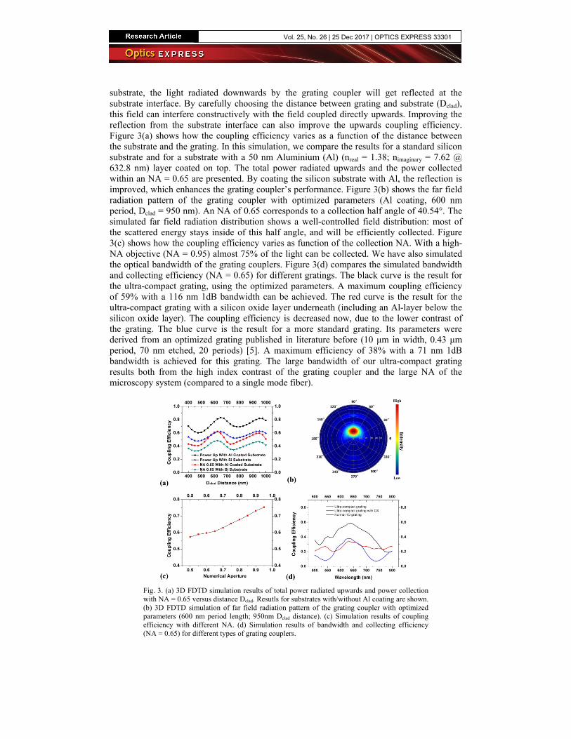
substrate, the light radiated downwards by the grating coupler will get reflected at the substrate interface. By carefully choosing the distance between grating and substrate (Dclad), this field can interfere constructively with the field coupled directly upwards. Improving the reflection from the substrate interface can also improve the upwards coupling efficiency. Figure 3(a) shows how the coupling efficiency varies as a function of the distance between the substrate and the grating. In this simulation, we compare the results for a standard silicon substrate and for a substrate with a 50 nm Aluminium (Al) (nreal = 1.38; nimaginary = 7.62 @ 632.8 nm) layer coated on top. The total power radiated upwards and the power collected within an NA = 0.65 are presented. By coating the silicon substrate with Al, the reflection is improved, which enhances the grating coupler’s performance. Figure 3(b) shows the far field radiation pattern of the grating coupler with optimized parameters (Al coating, 600 nm period, Dclad = 950 nm). An NA of 0.65 corresponds to a collection half angle of 40.54°. The simulated far field radiation distribution shows a well-controlled field distribution: most of the scattered energy stays inside of this half angle, and will be efficiently collected. Figure 3(c) shows how the coupling efficiency varies as function of the collection NA. With a high-NA objective (NA = 0.95) almost 75% of the light can be collected. We have also simulated the optical bandwidth of the grating couplers. Figure 3(d) compares the simulated bandwidth and collecting efficiency (NA = 0.65) for different gratings. The black curve is the result for the ultra-compact grating, using the optimized parameters. A maximum coupling efficiency of 59% with a 116 nm 1dB bandwidth can be achieved. The red curve is the result for the ultra-compact grating with a silicon oxide layer underneath (including an Al-layer below the silicon oxide layer). The coupling efficiency is decreased now, due to the lower contrast of the grating. The blue curve is the result for a more standard grating. Its parameters were derived from an optimized grating published in literature before (10 μm in width, 0.43 μm period, 70 nm etched, 20 periods) [5]. A maximum efficiency of 38% with a 71 nm 1dB bandwidth is achieved for this grating. The large bandwidth of our ultra-compact grating results both from the high index contrast of the grating coupler and the large NA of the microscopy system (compared to a single mode fiber).
Fig. 3. (a) 3D FDTD simulation results of total power radiated upwards and power collection with NA = 0.65 versus distance Dclad. Resutls for substrates with/without Al coating are shown. (b) 3D FDTD simulation of far field radiation pattern of the grating coupler with optimized parameters (600 nm period length; 950nm Dclad distance). (c) Simulation results of coupling efficiency with different NA. (d) Simulation results of bandwidth and collecting efficiency (NA = 0.65) for different types of grating couplers.
Vol. 25, No. 26 | 25 Dec 2017 | OPTICS EXPRESS 33301
3. Fabrication
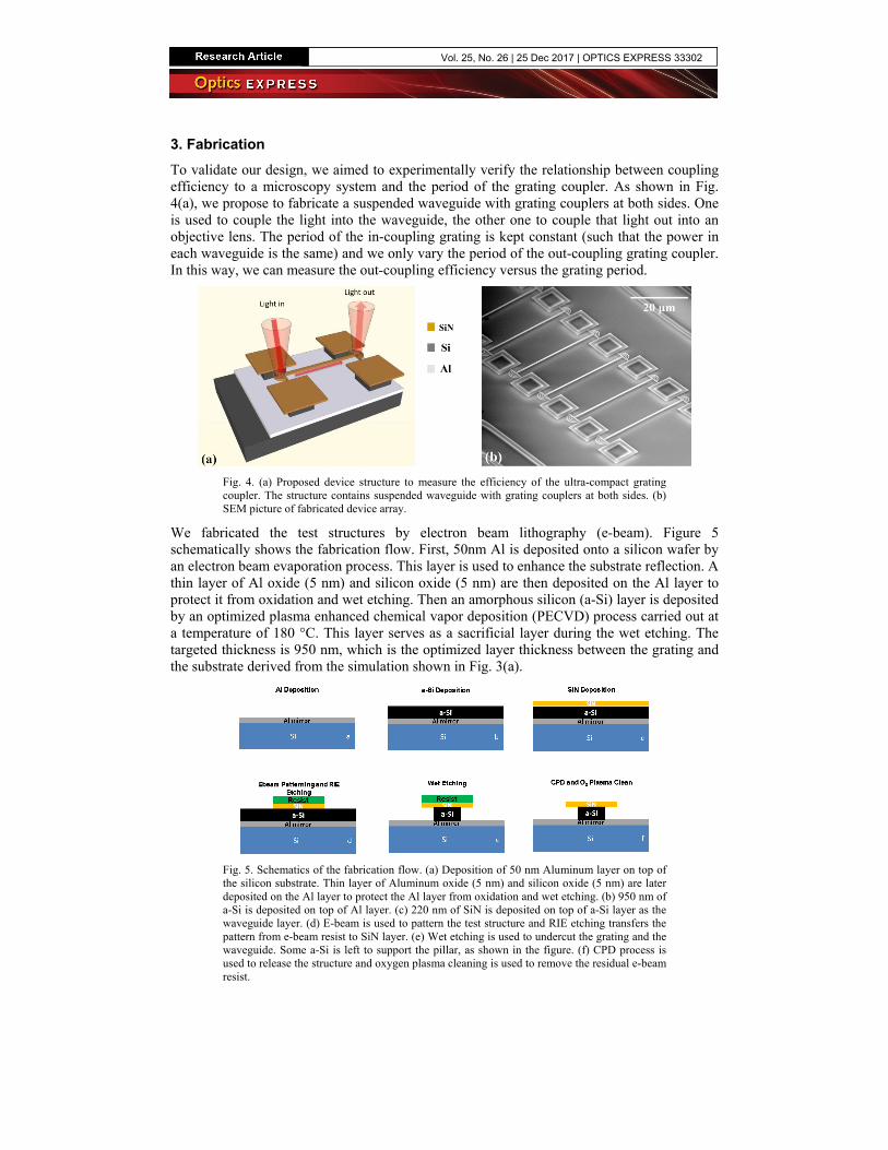
To validate our design, we aimed to experimentally verify the relationship between coupling efficiency to a microscopy system and the period of the grating coupler. As shown in Fig. 4(a), we propose to fabricate a suspended waveguide with grating couplers at both sides. One is used to couple the light into the waveguide, the other one to couple that light out into an objective lens. The period of the in-coupling grating is kept constant (such that the power in each waveguide is the same) and we only vary the period of the out-coupling grating coupler. In this way, we can measure the out-coupling efficiency versus the grating period.
Fig. 4. (a) Proposed device structure to measure the efficiency of the ultra-compact grating coupler. The structure contains suspended waveguide with grating couplers at both sides. (b) SEM picture of fabricated device array.
We fabricated the test structures by electron beam lithography (e-beam). Figure 5 schematically shows the fabrication flow. First, 50nm Al is deposited onto a silicon wafer by an electron beam evaporation process. This layer is used to enhance the substrate reflection. A thin layer of Al oxide (5 nm) and silicon oxide (5 nm) are then deposited on the Al layer to protect it from oxidation and wet etching. Then an amorphous silicon (a-Si) layer is deposited by an optimized plasma enhanced chemical vapor deposition (PECVD) process carried out at a temperature of 180 °C. This layer serves as a sacrificial layer during the wet etching. The targeted thickness is 950 nm, which is the optimized layer thickness between the grating and the substrate derived from the simulation shown in Fig. 3(a).
Fig. 5. Schematics of the fabrication flow. (a) Deposition of 50 nm Aluminum layer on top of the silicon substrate. Thin layer of Aluminum oxide (5 nm) and silicon oxide (5 nm) are later deposited on the Al layer to protect the Al layer from oxidation and wet etching. (b) 950 nm of a-Si is deposited on top of Al layer. (c) 220 nm of SiN is deposited on top of a-Si layer as the waveguide layer. (d) E-beam is used to pattern the test structure and RIE etching transfers the pattern from e-beam resist to SiN layer. (e) Wet etching is used to undercut the grating and the waveguide. Some a-Si is left to support the pillar, as shown in the figure. (f) CPD process is used to release the structure and oxygen plasma cleaning is used to remove the residual e-beam resist.
Vol. 25, No. 26 | 25 Dec 2017 | OPTICS EXPRESS 33302
A 220nm thick SiN layer is then deposited onto the a-Si layer by a PECVD process, carried out at 180 °C and an RF bias of 30 W at 13.56 MHz. The latter is optimized to obtain tensile strain in the deposited SiN layer, which guarantees good suspension after releasing the whole structure. Next, the grating coupler and waveguide structures are patterned using electron beam lithography (Raith Voyager). As mentioned in Section 2, a small beam (280nm in length) is added at each side, between the grating coupler and the waveguide, to support the whole structure with the attached pillars. The length of the suspended waveguide has been set to 35 μm, ensuring sufficient separation of the input and output grating couplers, while being short enough to avoid the collapsing of the structure. An optimized reactive ion etching (RIE) process is used to transfer the pattern to the SiN layer [18]. An alkaline based Tetramethylammonium hydroxide (TMAH) wet etch step is carried out at 65°C to remove the a-Si layer. Then a critical point drying (CPD) process is carried out to release the structure. Finally, an oxygen plasma cleaning is used to remove the residual e-beam resist. Figure 4(b) shows the scanning electron microscope (SEM) picture of the fabricated sample.
4. Characterization
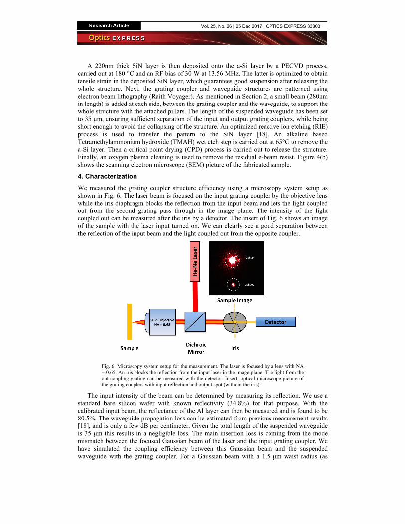
We measured the grating coupler structure efficiency using a microscopy system setup as shown in Fig. 6. The laser beam is focused on the input grating coupler by the objective lens while the iris diaphragm blocks the reflection from the input beam and lets the light coupled out from the second grating pass through in the image plane. The intensity of the light coupled out can be measured after the iris by a detector. The insert of Fig. 6 shows an image of the sample with the laser input turned on. We can clearly see a good separation between the reflection of the input beam and the light coupled out from the opposite coupler.
Fig. 6. Microscopy system setup for the measurement. The laser is focused by a lens with NA = 0.65. An iris blocks the reflection from the input laser in the image plane. The light from the out coupling grating can be measured with the detector. Insert: optical microscope picture of the grating couplers with input reflection and output spot (without the iris).
The input intensity of the beam can be determined by measuring its reflection. We use a standard bare silicon wafer with known reflectivity (34.8%) for that purpose. With the calibrated input beam, the reflectance of the Al layer can then be measured and is found to be 80.5%. The waveguide propagation loss can be estimated from previous measurement results [18], and is only a few dB per centimeter. Given the total length of the suspended waveguide is 35 μm this results in a negligible loss. The main insertion loss is coming from the mode mismatch between the focused Gaussian beam of the laser and the input grating coupler. We have simulated the coupling efficiency between this Gaussian beam and the suspended waveguide with the grating coupler. For a Gaussian beam with a 1.5 μm waist radius (as
Vol. 25, No. 26 | 25 Dec 2017 | OPTICS EXPRESS 33303

measured), 15.9% of the light can be coupled to the fundamental TE mode through the grating structure with 560 nm period, which was used as the input. This result is fairly robust against small variations in the grating coupler parameters. Figure 7 shows the measured coupling efficiency versus the period of the second grating coupler. Also the simulated coupling efficiency is shown. As expected, the coupling efficiency is strongly dependent on the grating coupler’s period. The maximum efficiency is achieved for a period of 620 nm, in which case 53% of the light from the TE mode from the waveguide can be coupled out by the grating coupler to the microscope. The measured results agree well with the simulated results. The remaining difference with simulated results might be related to an overestimation of the light coupled in the input grating coupler or small deviations in the fabricated structure and in particular the exact distance towards the substrate.
Fig. 7. Measurement results: the black curve is the simulated power couple to a microscopy system with NA = 0.65; the blue curve is the measured results with a 950 nm distance between the grating coupler and the Al substrate.
5. Conclusion and discussion
In conclusion, we have demonstrated the design, fabrication and characterization of an ultra-compact SiN grating coupler. The grating coupler is designed to maximize the coupling between a suspended SiN waveguide and a microscopy system. With the optimized parameters and using only 3 periods, we have experimentally demonstrated a 53% coupling efficiency from the fundamental TE mode (@ 632.8 nm) to a microscopy system with 0.65 NA. Simulations show that for an NA = 0.95 it should be possible to increase the coupling efficiency above 75%. Around 116 nm 1dB bandwidth can be theoretically achieved, due to the high contrast of the grating and the large collection angle provided by the microscopy system. The coupling efficiency can be further improved by using a more complicated distributed Bragg reflector layer on top of the substrate to improve the reflection compared to the currently used Al-mirror. Using a lens with a larger NA will also improve the coupling efficiency. Using a non-uniform grating period can help to reduce the return loss and also further improve the coupling efficiency.
Funding
EU (ERC-ULPPIC and ICT-NAVOLCHI); Belgian Science Policy Office (IAP).
Vol. 25, No. 26 | 25 Dec 2017 | OPTICS EXPRESS 33304