Embed Size (px)
Citation preview
This is information on a product in full production.
April 2016 DocID024330 Rev 4 1/129
STM32L151x6/8/B-A STM32L152x6/8/B-A
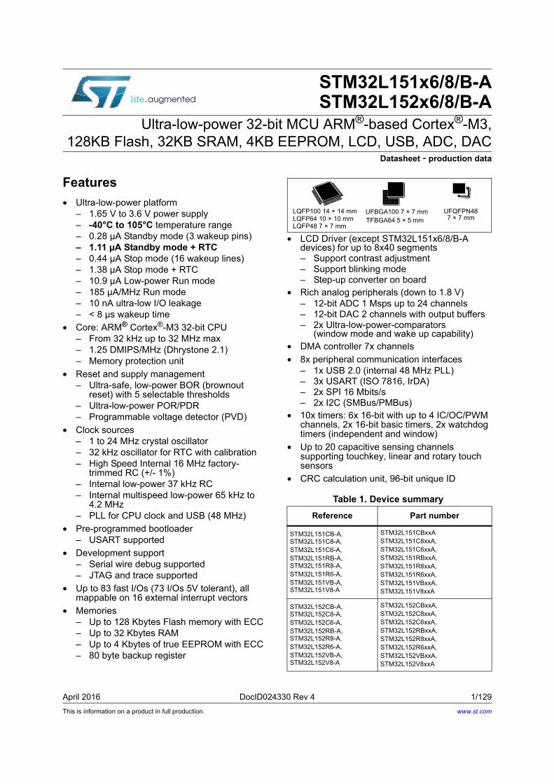
Ultra-low-power 32-bit MCU ARM®-based Cortex®-M3, 128KB Flash, 32KB SRAM, 4KB EEPROM, LCD, USB, ADC, DAC
Datasheet - production data
Features
• Ultra-low-power platform– 1.65 V to 3.6 V power supply– -40°C to 105°C temperature range– 0.28 µA Standby mode (3 wakeup pins)– 1.11 µA Standby mode + RTC– 0.44 µA Stop mode (16 wakeup lines)– 1.38 µA Stop mode + RTC– 10.9 µA Low-power Run mode– 185 µA/MHz Run mode– 10 nA ultra-low I/O leakage– < 8 µs wakeup time
• Core: ARM® Cortex®-M3 32-bit CPU– From 32 kHz up to 32 MHz max – 1.25 DMIPS/MHz (Dhrystone 2.1)– Memory protection unit
• Reset and supply management– Ultra-safe, low-power BOR (brownout
reset) with 5 selectable thresholds– Ultra-low-power POR/PDR– Programmable voltage detector (PVD)
• Clock sources– 1 to 24 MHz crystal oscillator– 32 kHz oscillator for RTC with calibration– High Speed Internal 16 MHz factory-
trimmed RC (+/- 1%)– Internal low-power 37 kHz RC– Internal multispeed low-power 65 kHz to
4.2 MHz– PLL for CPU clock and USB (48 MHz)
• Pre-programmed bootloader– USART supported
• Development support– Serial wire debug supported– JTAG and trace supported
• Up to 83 fast I/Os (73 I/Os 5V tolerant), all mappable on 16 external interrupt vectors
• Memories– Up to 128 Kbytes Flash memory with ECC– Up to 32 Kbytes RAM– Up to 4 Kbytes of true EEPROM with ECC– 80 byte backup register
• LCD Driver (except STM32L151x6/8/B-A devices) for up to 8x40 segments– Support contrast adjustment– Support blinking mode– Step-up converter on board
• Rich analog peripherals (down to 1.8 V)– 12-bit ADC 1 Msps up to 24 channels– 12-bit DAC 2 channels with output buffers– 2x Ultra-low-power-comparators
(window mode and wake up capability)• DMA controller 7x channels
• 8x peripheral communication interfaces– 1x USB 2.0 (internal 48 MHz PLL)– 3x USART (ISO 7816, IrDA)– 2x SPI 16 Mbits/s– 2x I2C (SMBus/PMBus)
• 10x timers: 6x 16-bit with up to 4 IC/OC/PWM channels, 2x 16-bit basic timers, 2x watchdog timers (independent and window)
• Up to 20 capacitive sensing channels supporting touchkey, linear and rotary touch sensors
• CRC calculation unit, 96-bit unique ID
Table 1. Device summary
Reference Part number
STM32L151CB-A, STM32L151C8-A,STM32L151C6-A,STM32L151RB-A, STM32L151R8-A,STM32L151R6-A,STM32L151VB-A, STM32L151V8-A
STM32L151CBxxASTM32L151C8xxA,STM32L151C6xxA, STM32L151RBxxA,STM32L151R8xxA, STM32L151R6xxA,STM32L151VBxxA,STM32L151V8xxA
STM32L152CB-A, STM32L152C8-A,STM32L152C6-A,STM32L152RB-A, STM32L152R8-A,STM32L152R6-A,STM32L152VB-A, STM32L152V8-A
STM32L152CBxxA,STM32L152C8xxA, STM32L152C6xxA,STM32L152RBxxA, STM32L152R8xxA,STM32L152R6xxA,STM32L152VBxxA,STM32L152V8xxA
LQFP100 14 × 14 mm LQFP64 10 × 10 mm LQFP48 7 × 7 mm
UFBGA100 7 × 7 mm UFQFPN48 7 × 7 mmTFBGA64 5 × 5 mm
www.st.com
Contents STM32L151x6/8/B-A STM32L152x6/8/B-A
2/129 DocID024330 Rev 4
Contents
1 Introduction . . . . . . . . . . . . . . . . . . . . . . . . . . . . . . . . . . . . . . . . . . . . . . . . 9
2 Description . . . . . . . . . . . . . . . . . . . . . . . . . . . . . . . . . . . . . . . . . . . . . . . . 10
2.1 Device overview . . . . . . . . . . . . . . . . . . . . . . . . . . . . . . . . . . . . . . . . . . . . .11
2.2 Ultra-low-power device continuum . . . . . . . . . . . . . . . . . . . . . . . . . . . . . . 12
2.2.1 Performance . . . . . . . . . . . . . . . . . . . . . . . . . . . . . . . . . . . . . . . . . . . . . 12
2.2.2 Shared peripherals . . . . . . . . . . . . . . . . . . . . . . . . . . . . . . . . . . . . . . . . 12
2.2.3 Common system strategy . . . . . . . . . . . . . . . . . . . . . . . . . . . . . . . . . . . 12
2.2.4 Features . . . . . . . . . . . . . . . . . . . . . . . . . . . . . . . . . . . . . . . . . . . . . . . . . 12
3 Functional overview . . . . . . . . . . . . . . . . . . . . . . . . . . . . . . . . . . . . . . . . 13
3.1 Low-power modes . . . . . . . . . . . . . . . . . . . . . . . . . . . . . . . . . . . . . . . . . . 14
3.2 ARM® Cortex®-M3 core with MPU . . . . . . . . . . . . . . . . . . . . . . . . . . . . . . 18
3.3 Reset and supply management . . . . . . . . . . . . . . . . . . . . . . . . . . . . . . . . 19
3.3.1 Power supply schemes . . . . . . . . . . . . . . . . . . . . . . . . . . . . . . . . . . . . . 19
3.3.2 Power supply supervisor . . . . . . . . . . . . . . . . . . . . . . . . . . . . . . . . . . . . 19
3.3.3 Voltage regulator . . . . . . . . . . . . . . . . . . . . . . . . . . . . . . . . . . . . . . . . . . 20
3.3.4 Boot modes . . . . . . . . . . . . . . . . . . . . . . . . . . . . . . . . . . . . . . . . . . . . . . 20
3.4 Clock management . . . . . . . . . . . . . . . . . . . . . . . . . . . . . . . . . . . . . . . . . 21
3.5 Low-power real-time clock and backup registers . . . . . . . . . . . . . . . . . . . 23
3.6 GPIOs (general-purpose inputs/outputs) . . . . . . . . . . . . . . . . . . . . . . . . . 23
3.7 Memories . . . . . . . . . . . . . . . . . . . . . . . . . . . . . . . . . . . . . . . . . . . . . . . . . 24
3.8 DMA (direct memory access) . . . . . . . . . . . . . . . . . . . . . . . . . . . . . . . . . . 24
3.9 LCD (liquid crystal display) . . . . . . . . . . . . . . . . . . . . . . . . . . . . . . . . . . . . 25
3.10 ADC (analog-to-digital converter) . . . . . . . . . . . . . . . . . . . . . . . . . . . . . . . 25
3.10.1 Temperature sensor . . . . . . . . . . . . . . . . . . . . . . . . . . . . . . . . . . . . . . . . 26
3.10.2 Internal voltage reference (VREFINT) . . . . . . . . . . . . . . . . . . . . . . . . . . . 26
3.11 DAC (digital-to-analog converter) . . . . . . . . . . . . . . . . . . . . . . . . . . . . . . . 26
3.12 Ultra-low-power comparators and reference voltage . . . . . . . . . . . . . . . . 27
3.13 Routing interface . . . . . . . . . . . . . . . . . . . . . . . . . . . . . . . . . . . . . . . . . . . 27
3.14 Touch sensing . . . . . . . . . . . . . . . . . . . . . . . . . . . . . . . . . . . . . . . . . . . . . 27
3.15 Timers and watchdogs . . . . . . . . . . . . . . . . . . . . . . . . . . . . . . . . . . . . . . . 27
DocID024330 Rev 4 3/129
STM32L151x6/8/B-A STM32L152x6/8/B-A Contents
4
3.15.1 General-purpose timers (TIM2, TIM3, TIM4, TIM9, TIM10 and TIM11) . 29
3.15.2 Basic timers (TIM6 and TIM7) . . . . . . . . . . . . . . . . . . . . . . . . . . . . . . . . 29
3.15.3 SysTick timer . . . . . . . . . . . . . . . . . . . . . . . . . . . . . . . . . . . . . . . . . . . . . 29
3.15.4 Independent watchdog (IWDG) . . . . . . . . . . . . . . . . . . . . . . . . . . . . . . . 29
3.15.5 Window watchdog (WWDG) . . . . . . . . . . . . . . . . . . . . . . . . . . . . . . . . . 30
3.16 Communication interfaces . . . . . . . . . . . . . . . . . . . . . . . . . . . . . . . . . . . . 30
3.16.1 I²C bus . . . . . . . . . . . . . . . . . . . . . . . . . . . . . . . . . . . . . . . . . . . . . . . . . . 30
3.16.2 Universal synchronous/asynchronous receiver transmitter (USART) . . 30
3.16.3 Serial peripheral interface (SPI) . . . . . . . . . . . . . . . . . . . . . . . . . . . . . . . 30
3.16.4 Universal serial bus (USB) . . . . . . . . . . . . . . . . . . . . . . . . . . . . . . . . . . . 30
3.17 CRC (cyclic redundancy check) calculation unit . . . . . . . . . . . . . . . . . . . 31
3.18 Development support . . . . . . . . . . . . . . . . . . . . . . . . . . . . . . . . . . . . . . . . 31
4 Pin descriptions . . . . . . . . . . . . . . . . . . . . . . . . . . . . . . . . . . . . . . . . . . . 32
5 Memory mapping . . . . . . . . . . . . . . . . . . . . . . . . . . . . . . . . . . . . . . . . . . . 51
6 Electrical characteristics . . . . . . . . . . . . . . . . . . . . . . . . . . . . . . . . . . . . 52
6.1 Parameter conditions . . . . . . . . . . . . . . . . . . . . . . . . . . . . . . . . . . . . . . . . 52
6.1.1 Minimum and maximum values . . . . . . . . . . . . . . . . . . . . . . . . . . . . . . . 52
6.1.2 Typical values . . . . . . . . . . . . . . . . . . . . . . . . . . . . . . . . . . . . . . . . . . . . 52
6.1.3 Typical curves . . . . . . . . . . . . . . . . . . . . . . . . . . . . . . . . . . . . . . . . . . . . 52
6.1.4 Loading capacitor . . . . . . . . . . . . . . . . . . . . . . . . . . . . . . . . . . . . . . . . . 52
6.1.5 Pin input voltage . . . . . . . . . . . . . . . . . . . . . . . . . . . . . . . . . . . . . . . . . . 52
6.1.6 Power supply scheme . . . . . . . . . . . . . . . . . . . . . . . . . . . . . . . . . . . . . . 53
6.1.7 Optional LCD power supply scheme . . . . . . . . . . . . . . . . . . . . . . . . . . . 54
6.1.8 Current consumption measurement . . . . . . . . . . . . . . . . . . . . . . . . . . . 54
6.2 Absolute maximum ratings . . . . . . . . . . . . . . . . . . . . . . . . . . . . . . . . . . . . 55
6.3 Operating conditions . . . . . . . . . . . . . . . . . . . . . . . . . . . . . . . . . . . . . . . . 56
6.3.1 General operating conditions . . . . . . . . . . . . . . . . . . . . . . . . . . . . . . . . . 56
6.3.2 Embedded reset and power control block characteristics . . . . . . . . . . . 57
6.3.3 Embedded internal reference voltage . . . . . . . . . . . . . . . . . . . . . . . . . . 59
6.3.4 Supply current characteristics . . . . . . . . . . . . . . . . . . . . . . . . . . . . . . . . 60
6.3.5 Wakeup time from Low-power mode . . . . . . . . . . . . . . . . . . . . . . . . . . . 70
6.3.6 External clock source characteristics . . . . . . . . . . . . . . . . . . . . . . . . . . . 72
6.3.7 Internal clock source characteristics . . . . . . . . . . . . . . . . . . . . . . . . . . . 77
6.3.8 PLL characteristics . . . . . . . . . . . . . . . . . . . . . . . . . . . . . . . . . . . . . . . . 79
Contents STM32L151x6/8/B-A STM32L152x6/8/B-A
4/129 DocID024330 Rev 4
6.3.9 Memory characteristics . . . . . . . . . . . . . . . . . . . . . . . . . . . . . . . . . . . . . 80
6.3.10 EMC characteristics . . . . . . . . . . . . . . . . . . . . . . . . . . . . . . . . . . . . . . . . 81
6.3.11 Electrical sensitivity characteristics . . . . . . . . . . . . . . . . . . . . . . . . . . . . 82
6.3.12 I/O current injection characteristics . . . . . . . . . . . . . . . . . . . . . . . . . . . . 83
6.3.13 I/O port characteristics . . . . . . . . . . . . . . . . . . . . . . . . . . . . . . . . . . . . . . 84
6.3.14 NRST pin characteristics . . . . . . . . . . . . . . . . . . . . . . . . . . . . . . . . . . . . 87
6.3.15 TIM timer characteristics . . . . . . . . . . . . . . . . . . . . . . . . . . . . . . . . . . . . 88
6.3.16 Communication interfaces . . . . . . . . . . . . . . . . . . . . . . . . . . . . . . . . . . . 89
6.3.17 12-bit ADC characteristics . . . . . . . . . . . . . . . . . . . . . . . . . . . . . . . . . . . 95
6.3.18 DAC electrical specifications . . . . . . . . . . . . . . . . . . . . . . . . . . . . . . . . 100
6.3.19 Temperature sensor characteristics . . . . . . . . . . . . . . . . . . . . . . . . . . . 102
6.3.20 Comparator . . . . . . . . . . . . . . . . . . . . . . . . . . . . . . . . . . . . . . . . . . . . . 103
6.3.21 LCD controller (STM32L152x6/8/B-A devices only) . . . . . . . . . . . . . . 105
7 Package information . . . . . . . . . . . . . . . . . . . . . . . . . . . . . . . . . . . . . . . 106
7.1 LQFP100 14 x 14 mm, 100-pin low-profile quad flat package information . . . . . . . . . . . . . . . . . . . . . . . . . . . . . . . . . . . . . . . . . . . . . . . 106
7.2 LQFP64 10 x 10 mm, 64-pin low-profile quad flat package information . 109
7.3 LQFP48 7 x 7 mm, 48-pin low-profile quad flat package information . . . .112
7.4 UFQFPN48 7 x 7 mm, 0.5 mm pitch, package information . . . . . . . . . . .115
7.5 UFBGA100 7 x 7 mm, 0.5 mm pitch, ultra thin fine-pitch ball grid array package information . . . . . . . . . . . . . . . . . . . . . . . . . . . . . . . . .118
7.6 TFBGA64 5 x 5 mm, 0.5 mm pitch, thin fine-pitch ball grid array package information . . . . . . . . . . . . . . . . . . . . . . . . . . . . . . . . . . . 121
7.7 Thermal characteristics . . . . . . . . . . . . . . . . . . . . . . . . . . . . . . . . . . . . . 124
7.7.1 Reference document . . . . . . . . . . . . . . . . . . . . . . . . . . . . . . . . . . . . . . 125
8 Ordering information . . . . . . . . . . . . . . . . . . . . . . . . . . . . . . . . . . . . . . 126
9 Revision history . . . . . . . . . . . . . . . . . . . . . . . . . . . . . . . . . . . . . . . . . . 127
DocID024330 Rev 4 5/129
STM32L151x6/8/B-A STM32L152x6/8/B-A List of tables
6
List of tables
Table 1. Device summary . . . . . . . . . . . . . . . . . . . . . . . . . . . . . . . . . . . . . . . . . . . . . . . . . . . . . . . . . . 1Table 2. Ultra-low-power STM32L151x6/8/B-A and STM32L152x6/8/B-A device features
and peripheral counts . . . . . . . . . . . . . . . . . . . . . . . . . . . . . . . . . . . . . . . . . . . . . . . . . . . . . 11Table 3. Functionalities depending on the operating power supply range . . . . . . . . . . . . . . . . . . . . 15Table 4. CPU frequency range depending on dynamic voltage scaling . . . . . . . . . . . . . . . . . . . . . . 16Table 5. Working mode-dependent functionalities (from Run/active down to standby) . . . . . . . . . . 17Table 6. VLCD rail decoupling . . . . . . . . . . . . . . . . . . . . . . . . . . . . . . . . . . . . . . . . . . . . . . . . . . . . . 25Table 7. Timer feature comparison. . . . . . . . . . . . . . . . . . . . . . . . . . . . . . . . . . . . . . . . . . . . . . . . . . 28Table 8. Legend/abbreviations used in the pinout table . . . . . . . . . . . . . . . . . . . . . . . . . . . . . . . . . . 38Table 9. STM32L151x6/8/B-A and STM32L152x6/8/B-A pin definitions . . . . . . . . . . . . . . . . . . . . . 39Table 10. Alternate function input/output . . . . . . . . . . . . . . . . . . . . . . . . . . . . . . . . . . . . . . . . . . . . . . 46Table 11. Voltage characteristics . . . . . . . . . . . . . . . . . . . . . . . . . . . . . . . . . . . . . . . . . . . . . . . . . . . . 55Table 12. Current characteristics . . . . . . . . . . . . . . . . . . . . . . . . . . . . . . . . . . . . . . . . . . . . . . . . . . . . 55Table 13. Thermal characteristics. . . . . . . . . . . . . . . . . . . . . . . . . . . . . . . . . . . . . . . . . . . . . . . . . . . . 56Table 14. General operating conditions . . . . . . . . . . . . . . . . . . . . . . . . . . . . . . . . . . . . . . . . . . . . . . . 56Table 15. Embedded reset and power control block characteristics. . . . . . . . . . . . . . . . . . . . . . . . . . 57Table 16. Embedded internal reference voltage calibration values . . . . . . . . . . . . . . . . . . . . . . . . . . 59Table 17. Embedded internal reference voltage. . . . . . . . . . . . . . . . . . . . . . . . . . . . . . . . . . . . . . . . . 59Table 18. Current consumption in Run mode, code with data processing running from Flash. . . . . . 61Table 19. Current consumption in Run mode, code with data processing running from RAM . . . . . . 62Table 20. Current consumption in Sleep mode . . . . . . . . . . . . . . . . . . . . . . . . . . . . . . . . . . . . . . . . . 63Table 21. Current consumption in Low-power run mode . . . . . . . . . . . . . . . . . . . . . . . . . . . . . . . . . . 64Table 22. Current consumption in Low-power sleep mode . . . . . . . . . . . . . . . . . . . . . . . . . . . . . . . . 65Table 23. Typical and maximum current consumptions in Stop mode . . . . . . . . . . . . . . . . . . . . . . . . 66Table 24. Typical and maximum current consumptions in Standby mode . . . . . . . . . . . . . . . . . . . . . 68Table 25. Peripheral current consumption . . . . . . . . . . . . . . . . . . . . . . . . . . . . . . . . . . . . . . . . . . . . . 69Table 26. Low-power mode wakeup timings . . . . . . . . . . . . . . . . . . . . . . . . . . . . . . . . . . . . . . . . . . . 71Table 27. High-speed external user clock characteristics. . . . . . . . . . . . . . . . . . . . . . . . . . . . . . . . . . 72Table 28. Low-speed external user clock characteristics . . . . . . . . . . . . . . . . . . . . . . . . . . . . . . . . . . 73Table 29. HSE oscillator characteristics . . . . . . . . . . . . . . . . . . . . . . . . . . . . . . . . . . . . . . . . . . . . . . . 73Table 30. LSE oscillator characteristics (fLSE = 32.768 kHz) . . . . . . . . . . . . . . . . . . . . . . . . . . . . . . . 75Table 31. HSI oscillator characteristics. . . . . . . . . . . . . . . . . . . . . . . . . . . . . . . . . . . . . . . . . . . . . . . . 77Table 32. LSI oscillator characteristics . . . . . . . . . . . . . . . . . . . . . . . . . . . . . . . . . . . . . . . . . . . . . . . . 77Table 33. MSI oscillator characteristics . . . . . . . . . . . . . . . . . . . . . . . . . . . . . . . . . . . . . . . . . . . . . . . 78Table 34. PLL characteristics . . . . . . . . . . . . . . . . . . . . . . . . . . . . . . . . . . . . . . . . . . . . . . . . . . . . . . . 79Table 35. RAM and hardware registers . . . . . . . . . . . . . . . . . . . . . . . . . . . . . . . . . . . . . . . . . . . . . . . 80Table 36. Flash memory and data EEPROM characteristics . . . . . . . . . . . . . . . . . . . . . . . . . . . . . . . 80Table 37. Flash memory, data EEPROM endurance and data retention . . . . . . . . . . . . . . . . . . . . . . 80Table 38. EMS characteristics . . . . . . . . . . . . . . . . . . . . . . . . . . . . . . . . . . . . . . . . . . . . . . . . . . . . . . 81Table 39. EMI characteristics . . . . . . . . . . . . . . . . . . . . . . . . . . . . . . . . . . . . . . . . . . . . . . . . . . . . . . . 82Table 40. ESD absolute maximum ratings . . . . . . . . . . . . . . . . . . . . . . . . . . . . . . . . . . . . . . . . . . . . . 82Table 41. Electrical sensitivities . . . . . . . . . . . . . . . . . . . . . . . . . . . . . . . . . . . . . . . . . . . . . . . . . . . . . 83Table 42. I/O current injection susceptibility . . . . . . . . . . . . . . . . . . . . . . . . . . . . . . . . . . . . . . . . . . . . 83Table 43. I/O static characteristics . . . . . . . . . . . . . . . . . . . . . . . . . . . . . . . . . . . . . . . . . . . . . . . . . . . 84Table 44. Output voltage characteristics . . . . . . . . . . . . . . . . . . . . . . . . . . . . . . . . . . . . . . . . . . . . . . 85Table 45. I/O AC characteristics . . . . . . . . . . . . . . . . . . . . . . . . . . . . . . . . . . . . . . . . . . . . . . . . . . . . . 86Table 46. NRST pin characteristics . . . . . . . . . . . . . . . . . . . . . . . . . . . . . . . . . . . . . . . . . . . . . . . . . . 87Table 47. TIMx characteristics . . . . . . . . . . . . . . . . . . . . . . . . . . . . . . . . . . . . . . . . . . . . . . . . . . . . . . 88
List of tables STM32L151x6/8/B-A STM32L152x6/8/B-A
6/129 DocID024330 Rev 4
Table 48. I2C characteristics. . . . . . . . . . . . . . . . . . . . . . . . . . . . . . . . . . . . . . . . . . . . . . . . . . . . . . . . 89Table 49. SCL frequency (fPCLK1= 32 MHz, VDD = VDD_I2C = 3.3 V). . . . . . . . . . . . . . . . . . . . . . . . 90Table 50. SPI characteristics . . . . . . . . . . . . . . . . . . . . . . . . . . . . . . . . . . . . . . . . . . . . . . . . . . . . . . . 91Table 51. USB startup time. . . . . . . . . . . . . . . . . . . . . . . . . . . . . . . . . . . . . . . . . . . . . . . . . . . . . . . . . 93Table 52. USB DC electrical characteristics . . . . . . . . . . . . . . . . . . . . . . . . . . . . . . . . . . . . . . . . . . . . 94Table 53. USB: full speed electrical characteristics . . . . . . . . . . . . . . . . . . . . . . . . . . . . . . . . . . . . . . 94Table 54. ADC clock frequency . . . . . . . . . . . . . . . . . . . . . . . . . . . . . . . . . . . . . . . . . . . . . . . . . . . . . 95Table 55. ADC characteristics . . . . . . . . . . . . . . . . . . . . . . . . . . . . . . . . . . . . . . . . . . . . . . . . . . . . . . 95Table 56. ADC accuracy. . . . . . . . . . . . . . . . . . . . . . . . . . . . . . . . . . . . . . . . . . . . . . . . . . . . . . . . . . . 97Table 57. Maximum source impedance RAIN max . . . . . . . . . . . . . . . . . . . . . . . . . . . . . . . . . . . . . . . 99Table 58. DAC characteristics . . . . . . . . . . . . . . . . . . . . . . . . . . . . . . . . . . . . . . . . . . . . . . . . . . . . . 100Table 59. Temperature sensor calibration values. . . . . . . . . . . . . . . . . . . . . . . . . . . . . . . . . . . . . . . 102Table 60. Temperature sensor characteristics . . . . . . . . . . . . . . . . . . . . . . . . . . . . . . . . . . . . . . . . . 102Table 61. Comparator 1 characteristics . . . . . . . . . . . . . . . . . . . . . . . . . . . . . . . . . . . . . . . . . . . . . . 103Table 62. Comparator 2 characteristics . . . . . . . . . . . . . . . . . . . . . . . . . . . . . . . . . . . . . . . . . . . . . . 104Table 63. LCD controller characteristics . . . . . . . . . . . . . . . . . . . . . . . . . . . . . . . . . . . . . . . . . . . . . . 105Table 64. LQPF100 14 x 14 mm, 100-pin low-profile quad flat package
mechanical data . . . . . . . . . . . . . . . . . . . . . . . . . . . . . . . . . . . . . . . . . . . . . . . . . . . . . . . . 107Table 65. LQFP64 10 x 10 mm, 64-pin low-profile quad flat package mechanical data. . . . . . . . . . 109Table 66. LQFP48 7 x 7 mm, 48-pin low-profile quad flat package mechanical data. . . . . . . . . . . . 113Table 67. UFQFPN48 7 x 7 mm, 0.5 mm pitch, package mechanical data . . . . . . . . . . . . . . . . . . . 116Table 68. UFBGA100 7 x 7 mm, 0.5 mm pitch, ultra thin fine-pitch ball grid array
package mechanical data . . . . . . . . . . . . . . . . . . . . . . . . . . . . . . . . . . . . . . . . . . . . . . . . . 118Table 69. UFBGA100 7 x 7 mm, 0.5 mm pitch, recommended PCB design rules . . . . . . . . . . . . . . 119Table 70. TFBGA64 5 x 5 mm, 0.5 mm pitch, thin fine-pitch ball grid array
package mechanical data . . . . . . . . . . . . . . . . . . . . . . . . . . . . . . . . . . . . . . . . . . . . . . . . . 121Table 71. TFBGA64 5 x 5 mm, 0.5 mm pitch, recommended PCB design rules . . . . . . . . . . . . . . . 122Table 72. Thermal characteristics. . . . . . . . . . . . . . . . . . . . . . . . . . . . . . . . . . . . . . . . . . . . . . . . . . . 124Table 73. Ordering information scheme . . . . . . . . . . . . . . . . . . . . . . . . . . . . . . . . . . . . . . . . . . . . . . 126Table 74. Document revision history . . . . . . . . . . . . . . . . . . . . . . . . . . . . . . . . . . . . . . . . . . . . . . . . 127
DocID024330 Rev 4 7/129
STM32L151x6/8/B-A STM32L152x6/8/B-A List of figures
8
List of figures
Figure 1. Ultra-low-power STM32L151x6/8/B-A and STM32L152x6/8/B-A block diagram . . . . . . . . 13Figure 2. Clock tree . . . . . . . . . . . . . . . . . . . . . . . . . . . . . . . . . . . . . . . . . . . . . . . . . . . . . . . . . . . . . . 22Figure 3. STM32L15xVxxxA UFBGA100 ballout . . . . . . . . . . . . . . . . . . . . . . . . . . . . . . . . . . . . . . . . 32Figure 4. STM32L15xVxxxA LQFP100 pinout . . . . . . . . . . . . . . . . . . . . . . . . . . . . . . . . . . . . . . . . . . 33Figure 5. STM32L15xRxxxA TFBGA64 ballout . . . . . . . . . . . . . . . . . . . . . . . . . . . . . . . . . . . . . . . . . 34Figure 6. STM32L15xRxxxA LQFP64 pinout . . . . . . . . . . . . . . . . . . . . . . . . . . . . . . . . . . . . . . . . . . . 35Figure 7. STM32L15xCxxxA LQFP48 pinout . . . . . . . . . . . . . . . . . . . . . . . . . . . . . . . . . . . . . . . . . . 36Figure 8. STM32L15xCxxxA UFQFPN48 pinout . . . . . . . . . . . . . . . . . . . . . . . . . . . . . . . . . . . . . . . . 37Figure 9. Memory map. . . . . . . . . . . . . . . . . . . . . . . . . . . . . . . . . . . . . . . . . . . . . . . . . . . . . . . . . . . . 51Figure 10. Pin loading conditions. . . . . . . . . . . . . . . . . . . . . . . . . . . . . . . . . . . . . . . . . . . . . . . . . . . . . 52Figure 11. Pin input voltage . . . . . . . . . . . . . . . . . . . . . . . . . . . . . . . . . . . . . . . . . . . . . . . . . . . . . . . . . 52Figure 12. Power supply scheme. . . . . . . . . . . . . . . . . . . . . . . . . . . . . . . . . . . . . . . . . . . . . . . . . . . . . 53Figure 13. Optional LCD power supply scheme . . . . . . . . . . . . . . . . . . . . . . . . . . . . . . . . . . . . . . . . . 54Figure 14. Current consumption measurement scheme . . . . . . . . . . . . . . . . . . . . . . . . . . . . . . . . . . . 54Figure 15. High-speed external clock source AC timing diagram . . . . . . . . . . . . . . . . . . . . . . . . . . . . 72Figure 16. Low-speed external clock source AC timing diagram. . . . . . . . . . . . . . . . . . . . . . . . . . . . . 73Figure 17. HSE oscillator circuit diagram. . . . . . . . . . . . . . . . . . . . . . . . . . . . . . . . . . . . . . . . . . . . . . . 75Figure 18. Typical application with a 32.768 kHz crystal . . . . . . . . . . . . . . . . . . . . . . . . . . . . . . . . . . . 76Figure 19. I/O AC characteristics definition . . . . . . . . . . . . . . . . . . . . . . . . . . . . . . . . . . . . . . . . . . . . . 87Figure 20. Recommended NRST pin protection . . . . . . . . . . . . . . . . . . . . . . . . . . . . . . . . . . . . . . . . . 88Figure 21. I2C bus AC waveforms and measurement circuit . . . . . . . . . . . . . . . . . . . . . . . . . . . . . . . . 90Figure 22. SPI timing diagram - slave mode and CPHA = 0 . . . . . . . . . . . . . . . . . . . . . . . . . . . . . . . . 92Figure 23. SPI timing diagram - slave mode and CPHA = 1(1) . . . . . . . . . . . . . . . . . . . . . . . . . . . . . . 92Figure 24. SPI timing diagram - master mode(1) . . . . . . . . . . . . . . . . . . . . . . . . . . . . . . . . . . . . . . . . . 93Figure 25. USB timings: definition of data signal rise and fall time . . . . . . . . . . . . . . . . . . . . . . . . . . . 94Figure 26. ADC accuracy characteristics . . . . . . . . . . . . . . . . . . . . . . . . . . . . . . . . . . . . . . . . . . . . . . . 98Figure 27. Typical connection diagram using the ADC . . . . . . . . . . . . . . . . . . . . . . . . . . . . . . . . . . . . 98Figure 28. Maximum dynamic current consumption on VREF+ supply pin during ADC
conversion . . . . . . . . . . . . . . . . . . . . . . . . . . . . . . . . . . . . . . . . . . . . . . . . . . . . . . . . . . . . . 99Figure 29. 12-bit buffered /non-buffered DAC . . . . . . . . . . . . . . . . . . . . . . . . . . . . . . . . . . . . . . . . . . 102Figure 30. LQFP100 14 x 14 mm, 100-pin low-profile quad flat package outline . . . . . . . . . . . . . . . 106Figure 31. LQPF100 14 x 14 mm, 100-pin low-profile quad flat package recommended footprint . . 108Figure 32. LQFP100 14 x 14 mm, 100-pin package top view example . . . . . . . . . . . . . . . . . . . . . . . 108Figure 33. LQFP64 10 x 10 mm, 64-pin low-profile quad flat package outline . . . . . . . . . . . . . . . . . 109Figure 34. LQFP64 10 x 10 mm, 64-pin low-profile quad flat package recommended footprint . . . . 110Figure 35. LQFP64 10 x 10 mm, 64-pin low-profile quad flat package top view example . . . . . . . . . 111Figure 36. LQFP48 7 x 7 mm, 48-pin low-profile quad flat package outline . . . . . . . . . . . . . . . . . . . 112Figure 37. LQFP48 7 x 7 mm, 48-pin low-profile quad flat package recommended footprint . . . . . . 114Figure 38. LQFP48 7 x 7 mm, 48-pin low-profile quad flat package top view example . . . . . . . . . . . 114Figure 39. UFQFPN48 7 x 7 mm, 0.5 mm pitch, package outline . . . . . . . . . . . . . . . . . . . . . . . . . . . 115Figure 40. UFQFPN48 7 x 7 mm, 0.5 mm pitch, package recommended footprint . . . . . . . . . . . . . . 116Figure 41. UFQFPN48 7 x 7 mm, 0.5 mm pitch, package top view example . . . . . . . . . . . . . . . . . . 117Figure 42. UFBGA100, 7 x 7 mm, 0.5 mm pitch, ultra thin fine-pitch ball grid array
package outline. . . . . . . . . . . . . . . . . . . . . . . . . . . . . . . . . . . . . . . . . . . . . . . . . . . . . . . . . 118Figure 43. UFBGA100 7 x 7 mm, 0.5 mm pitch, ultra thin fine-pitch ball grid array
package recommended footprint . . . . . . . . . . . . . . . . . . . . . . . . . . . . . . . . . . . . . . . . . . . 119Figure 44. UFBGA100 7 x 7 mm, 0.5 mm pitch, package top view example. . . . . . . . . . . . . . . . . . . 120Figure 45. TFBGA64 5 x 5 mm, 0.5 mm pitch, thin fine-pitch ball grid array
List of figures STM32L151x6/8/B-A STM32L152x6/8/B-A
8/129 DocID024330 Rev 4
package outline. . . . . . . . . . . . . . . . . . . . . . . . . . . . . . . . . . . . . . . . . . . . . . . . . . . . . . . . . 121Figure 46. TFBGA64, 5 x 5 mm, 0.5 mm pitch, thin fine-pitch ball grid array
package recommended footprint . . . . . . . . . . . . . . . . . . . . . . . . . . . . . . . . . . . . . . . . . . . 122Figure 47. TFBGA64 5 x 5 mm, 0.5 mm pitch, package top view example . . . . . . . . . . . . . . . . . . . . 123Figure 48. Thermal resistance suffix 6 . . . . . . . . . . . . . . . . . . . . . . . . . . . . . . . . . . . . . . . . . . . . . . . . 125Figure 49. Thermal resistance suffix 7 . . . . . . . . . . . . . . . . . . . . . . . . . . . . . . . . . . . . . . . . . . . . . . . . 125
DocID024330 Rev 4 9/129
STM32L151x6/8/B-A STM32L152x6/8/B-A Introduction
51
1 Introduction
This datasheet provides the ordering information and mechanical device characteristics of the STM32L151x6/8/B-A and STM32L152x6/8/B-A ultra-low-power ARM® Cortex®-M3 based microcontrollers product line.
The ultra-low-power STM32L151x6/8/B-A and STM32L152x6/8/B-A microcontroller family includes devices in 3 different package types: from 48 to 100 pins. Depending on the device chosen, different sets of peripherals are included, the description below gives an overview of the complete range of peripherals proposed in this family.
These features make the ultra-low-power STM32L151x6/8/B-A and STM32L152x6/8/B-A microcontroller family suitable for a wide range of applications:
• Medical and handheld equipment
• Application control and user interface
• PC peripherals, gaming, GPS and sport equipment
• Alarm systems, Wired and wireless sensors, Video intercom
• Utility metering
This STM32L151x6/8/B-A and STM32L152x6/8/B-A datasheet should be read in conjunction with the STM32L1xxxx reference manual (RM0038). The document "Getting started with STM32L1xxxx hardware development” AN3216 gives a hardware implementation overview.
Both documents are available from the STMicroelectronics website www.st.com.
For information on the ARM® Cortex®-M3 core please refer to the Cortex®-M3 Technical Reference Manual, available from the ARM website.
Figure 1 shows the general block diagram of the device family.
Caution: This datasheet does not apply to:
– STM32L15xx6/8/B
covered by a separate datasheet.
Description STM32L151x6/8/B-A STM32L152x6/8/B-A
10/129 DocID024330 Rev 4
2 Description
The ultra-low-power STM32L151x6/8/B-A and STM32L152x6/8/B-A devices incorporate the connectivity power of the universal serial bus (USB) with the high-performance ARM® Cortex®-M3 32-bit RISC core operating at a frequency of 32 MHz (33.3 DMIPS), a memory protection unit (MPU), high-speed embedded memories (Flash memory up to 128 Kbytes and RAM up to 32 Kbytes) and an extensive range of enhanced I/Os and peripherals connected to two APB buses.
All the devices offer a 12-bit ADC, 2 DACs and 2 ultra-low-power comparators, six general-purpose 16-bit timers and two basic timers, which can be used as time bases.
Moreover, the STM32L151x6/8/B-A and STM32L152x6/8/B-A devices contain standard and advanced communication interfaces: up to two I2Cs and SPIs, three USARTs and a USB. The STM32L151x6/8/B-A and STM32L152x6/8/B-A devices offer up to 20 capacitive sensing channels to simply add touch sensing functionality to any application.
They also include a real-time clock with sub-second counting and a set of backup registers that remain powered in Standby mode.
Finally, the integrated LCD controller (except STM32L151x6/8/B-A devices) has a built-in LCD voltage generator that allows to drive up to 8 multiplexed LCDs with contrast independent of the supply voltage.
The ultra-low-power STM32L151x6/8/B-A and STM32L152x6/8/B-A devices operate from a 1.8 to 3.6 V power supply (down to 1.65 V at power down) with BOR and from a 1.65 to 3.6 V power supply without BOR option. They are available in the -40 to +85 °C and -40 to +105°C temperature ranges. A comprehensive set of power-saving modes allows the design of low-power applications.
DocID024330 Rev 4 11/129
STM32L151x6/8/B-A STM32L152x6/8/B-A Description
51
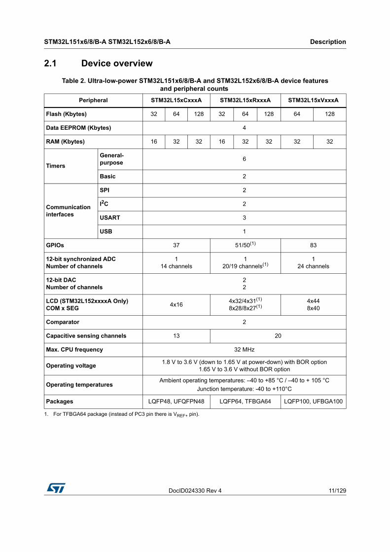
2.1 Device overview
Table 2. Ultra-low-power STM32L151x6/8/B-A and STM32L152x6/8/B-A device featuresand peripheral counts
Peripheral STM32L15xCxxxA STM32L15xRxxxA STM32L15xVxxxA
Flash (Kbytes) 32 64 128 32 64 128 64 128
Data EEPROM (Kbytes) 4
RAM (Kbytes) 16 32 32 16 32 32 32 32
Timers
General-purpose
6
Basic 2
Communication interfaces
SPI 2
I2C 2
USART 3
USB 1
GPIOs 37 51/50(1) 83
12-bit synchronized ADC Number of channels
114 channels
120/19 channels(1)
124 channels
12-bit DAC Number of channels
22
LCD (STM32L152xxxxA Only) COM x SEG
4x164x32/4x31(1)
8x28/8x27(1)4x448x40
Comparator 2
Capacitive sensing channels 13 20
Max. CPU frequency 32 MHz
Operating voltage1.8 V to 3.6 V (down to 1.65 V at power-down) with BOR option
1.65 V to 3.6 V without BOR option
Operating temperaturesAmbient operating temperatures: –40 to +85 °C / –40 to + 105 °C
Junction temperature: -40 to +110°C
Packages LQFP48, UFQFPN48 LQFP64, TFBGA64 LQFP100, UFBGA100
1. For TFBGA64 package (instead of PC3 pin there is VREF+ pin).
Description STM32L151x6/8/B-A STM32L152x6/8/B-A
12/129 DocID024330 Rev 4
2.2 Ultra-low-power device continuum
The ultra-low-power family offers a large choice of cores and features. From a proprietary 8-bit core up to the Cortex-M3, including the Cortex-M0+, the STM8Lx and STM32Lx series offer the best range of choices to meet your requirements in terms of ultra-low-power features. The STM32 Ultra-low-power series is an ideal fit for applications like gas/water meters, keyboard/mouse, or wearable devices for fitness and healthcare. Numerous built-in features like LCD drivers, dual-bank memory, low-power Run mode, op-amp, AES-128bit, DAC, crystal-less USB and many others, allow to build highly cost-optimized applications by reducing the BOM.
Note: STMicroelectronics as a reliable and long-term manufacturer ensures as much as possible the pin-to-pin compatibility between any STM8Lx and STM32Lx devices and between any of the STM32Lx and STM32Fx series. Thanks to this unprecedented scalability, your existing applications can be upgraded to respond to the latest market features and efficiency demand.
2.2.1 Performance
All families incorporate highly energy-efficient cores with both Harvard architecture and pipelined execution: advanced STM8 core for STM8L families and ARM Cortex-M3 core for STM32L family. In addition specific care for the design architecture has been taken to optimize the mA/DMIPS and mA/MHz ratios.
This allows the ultra-Low-power performance to range from 5 up to 33.3 DMIPs.
2.2.2 Shared peripherals
STM8L15xxx and STM32L1xxxx share identical peripherals which ensure a very easy migration from one family to another:
• Analog peripherals: ADC, DAC and comparators
• Digital peripherals: RTC and some communication interfaces
2.2.3 Common system strategy
To offer flexibility and optimize performance, the STM8L15xxx and STM32L1xxxx families use a common architecture:
• Common power supply range from 1.65 V to 3.6 V, (1.65 V at power down only for STM8L15xxx devices)
• Architecture optimized to reach ultra-low consumption both in low-power modes and Run mode
• Fast startup strategy from low-power modes
• Flexible system clock
• Ultra-safe reset: same reset strategy including power-on reset, power-down reset, brownout reset and programmable voltage detector.
2.2.4 Features
ST ultra-low-power continuum also lies in feature compatibility:
• More than 10 packages with pin count from 20 to 144 pins and size down to 3 x 3 mm
• Memory density ranging from 4 to 512 Kbytes
DocID024330 Rev 4 13/129
STM32L151x6/8/B-A STM32L152x6/8/B-A Functional overview
51
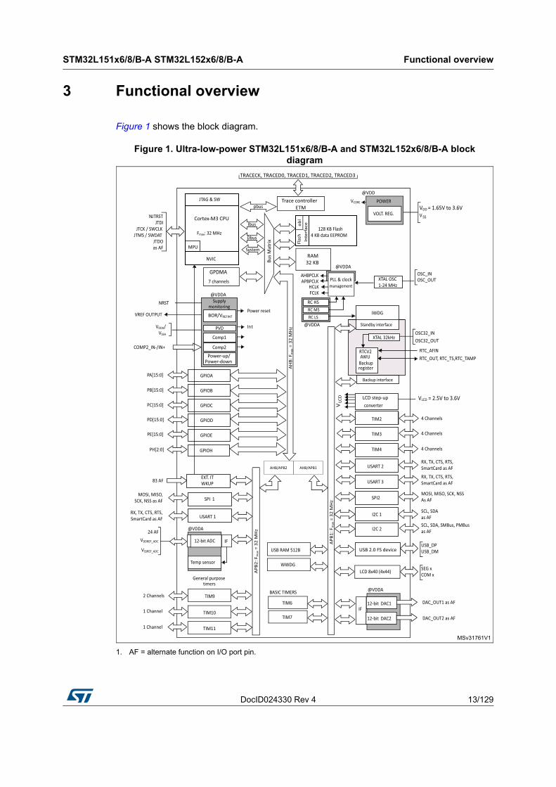
3 Functional overview
Figure 1 shows the block diagram.
Figure 1. Ultra-low-power STM32L151x6/8/B-A and STM32L152x6/8/B-A block diagram
1. AF = alternate function on I/O port pin.
Functional overview STM32L151x6/8/B-A STM32L152x6/8/B-A
14/129 DocID024330 Rev 4
3.1 Low-power modes
The ultra-low-power STM32L151x6/8/B-A and STM32L152x6/8/B-A devices support dynamic voltage scaling to optimize its power consumption in run mode. The voltage from the internal low-drop regulator that supplies the logic can be adjusted according to the system’s maximum operating frequency and the external voltage supply:
• In Range 1 (VDD range limited to 1.71-3.6 V), the CPU runs at up to 32 MHz (refer to Table 18 for consumption).
• In Range 2 (full VDD range), the CPU runs at up to 16 MHz (refer to Table 18 for consumption)
• In Range 3 (full VDD range), the CPU runs at up to 4 MHz (generated only with the multispeed internal RC oscillator clock source). Refer to Table 18 for consumption.
Seven low-power modes are provided to achieve the best compromise between low-power consumption, short startup time and available wakeup sources:
• Sleep mode
In Sleep mode, only the CPU is stopped. All peripherals continue to operate and can wake up the CPU when an interrupt/event occurs.
Sleep mode power consumption: refer to Table 20.
• Low-power Run mode
This mode is achieved with the multispeed internal (MSI) RC oscillator set to the minimum clock (less than 131 kHz), execution from SRAM or Flash memory, and internal regulator in low-power mode to minimize the regulator's operating current. In the low-power Run mode, the clock frequency and the number of enabled peripherals are both limited.
Low-power Run mode consumption: refer to Table 21.
• Low-power Sleep mode
This mode is achieved by entering the Sleep mode with the internal voltage regulator in low-power mode to minimize the regulator’s operating current. In the low-power Sleep mode, both the clock frequency and the number of enabled peripherals are limited; a typical example would be to have a timer running at 32 kHz. When wakeup is triggered by an event or an interrupt, the system reverts to the run mode with the regulator on.
Low-power Sleep mode consumption: refer to Table 22.
• Stop mode with RTC
Stop mode achieves the lowest power consumption while retaining the RAM and register contents and real time clock. All clocks in the VCORE domain are stopped, the PLL, MSI RC, HSI RC and HSE crystal oscillators are disabled. The LSE or LSI is still running. The voltage regulator is in the low-power mode.
The device can be woken up from Stop mode by any of the EXTI line, in 8 µs. The EXTI line source can be one of the 16 external lines. It can be the PVD output, the Comparator 1 event or Comparator 2 event (if internal reference voltage is on), it can be the RTC alarm(s), the USB wakeup, the RTC tamper events, the RTC timestamp event or the RTC wakeup.
• Stop mode without RTC
Stop mode achieves the lowest power consumption while retaining the RAM and register contents. All clocks are stopped, the PLL, MSI RC, HSI and LSI RC, LSE and HSE crystal oscillators are disabled. The voltage regulator is in the low-power mode. The device can be woken up from Stop mode by any of the EXTI line, in 8 µs. The EXTI
DocID024330 Rev 4 15/129
STM32L151x6/8/B-A STM32L152x6/8/B-A Functional overview
51
line source can be one of the 16 external lines. It can be the PVD output, the Comparator 1 event or Comparator 2 event (if internal reference voltage is on). It can also be wakened by the USB wakeup.
Stop mode consumption: refer to Table 23.
• Standby mode with RTC
Standby mode is used to achieve the lowest power consumption and real time clock. The internal voltage regulator is switched off so that the entire VCORE domain is powered off. The PLL, MSI RC, HSI RC and HSE crystal oscillators are also switched off. The LSE or LSI is still running. After entering Standby mode, the RAM and register contents are lost except for registers in the Standby circuitry (wakeup logic, IWDG, RTC, LSI, LSE Crystal 32K osc, RCC_CSR).
The device exits Standby mode in 60 µs when an external reset (NRST pin), an IWDG reset, a rising edge on one of the three WKUP pins, RTC alarm (Alarm A or Alarm B), RTC tamper event, RTC timestamp event or RTC Wakeup event occurs.
• Standby mode without RTC
Standby mode is used to achieve the lowest power consumption. The internal voltage regulator is switched off so that the entire VCORE domain is powered off. The PLL, MSI, RC, HSI and LSI RC, HSE and LSE crystal oscillators are also switched off. After entering Standby mode, the RAM and register contents are lost except for registers in the Standby circuitry (wakeup logic, IWDG, RTC, LSI, LSE Crystal 32K osc, RCC_CSR).
The device exits Standby mode in 60 µs when an external reset (NRST pin) or a rising edge on one of the three WKUP pin occurs.
Standby mode consumption: refer to Table 24.
Note: The RTC, the IWDG, and the corresponding clock sources are not stopped by entering the Stop or Standby mode.
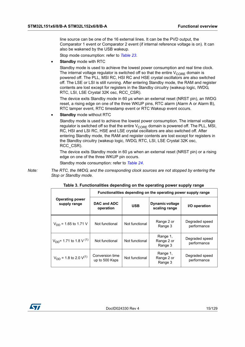
Table 3. Functionalities depending on the operating power supply range
Operating power supply range
Functionalities depending on the operating power supply range
DAC and ADC operation
USBDynamic voltage
scaling rangeI/O operation
VDD = 1.65 to 1.71 V Not functional Not functionalRange 2 or
Range 3Degraded speed
performance
VDD= 1.71 to 1.8 V (1) Not functional Not functionalRange 1,
Range 2 or Range 3
Degraded speed performance
VDD = 1.8 to 2.0 V(1) Conversion time up to 500 Ksps
Not functionalRange 1,
Range 2 or Range 3
Degraded speed performance
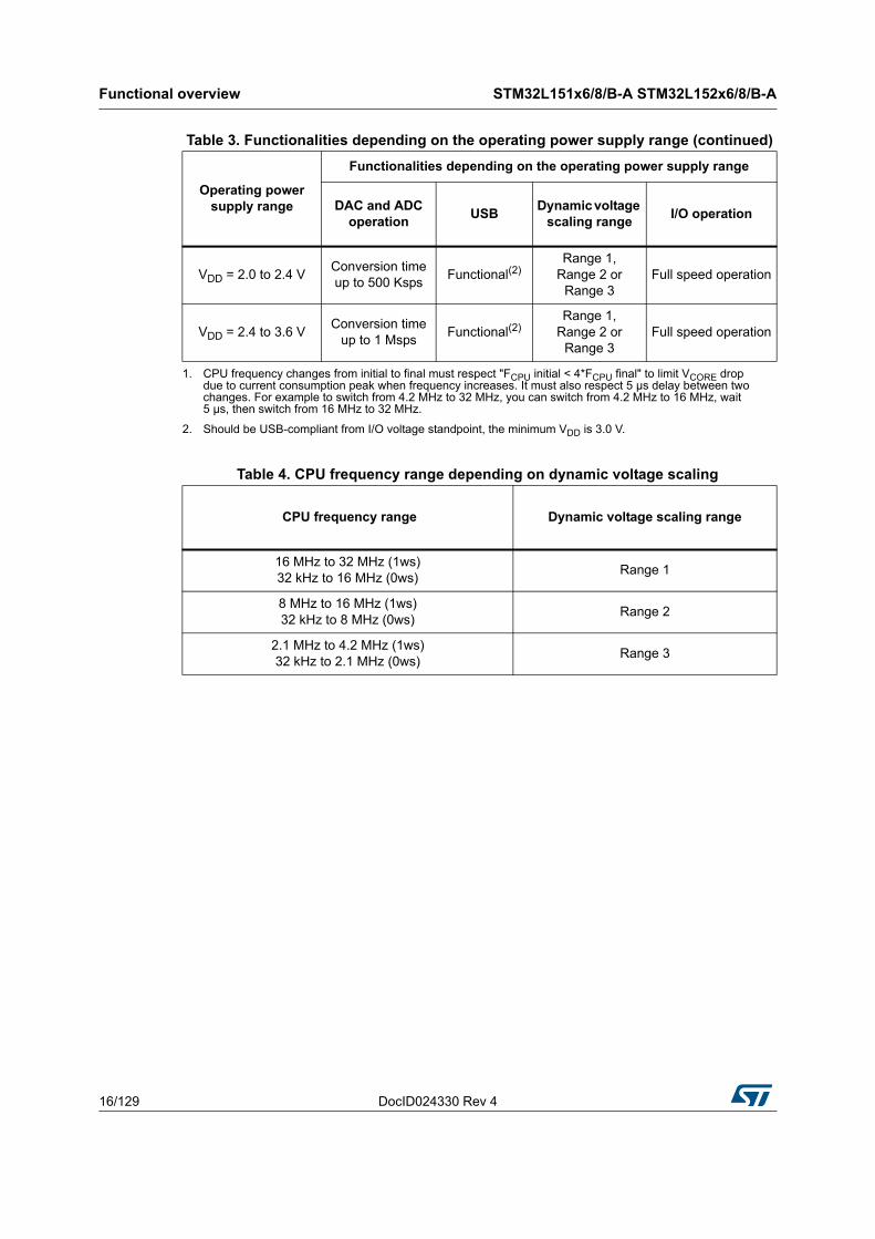
Functional overview STM32L151x6/8/B-A STM32L152x6/8/B-A
16/129 DocID024330 Rev 4
VDD = 2.0 to 2.4 VConversion time up to 500 Ksps
Functional(2)Range 1,
Range 2 or Range 3
Full speed operation
VDD = 2.4 to 3.6 VConversion time
up to 1 MspsFunctional(2)
Range 1, Range 2 or
Range 3Full speed operation
1. CPU frequency changes from initial to final must respect "FCPU initial < 4*FCPU final" to limit VCORE drop due to current consumption peak when frequency increases. It must also respect 5 µs delay between two changes. For example to switch from 4.2 MHz to 32 MHz, you can switch from 4.2 MHz to 16 MHz, wait 5 µs, then switch from 16 MHz to 32 MHz.
2. Should be USB-compliant from I/O voltage standpoint, the minimum VDD is 3.0 V.
Table 4. CPU frequency range depending on dynamic voltage scaling
CPU frequency range Dynamic voltage scaling range
16 MHz to 32 MHz (1ws)32 kHz to 16 MHz (0ws)
Range 1
8 MHz to 16 MHz (1ws)32 kHz to 8 MHz (0ws)
Range 2
2.1 MHz to 4.2 MHz (1ws)32 kHz to 2.1 MHz (0ws)
Range 3
Table 3. Functionalities depending on the operating power supply range (continued)
Operating power supply range
Functionalities depending on the operating power supply range
DAC and ADC operation
USBDynamic voltage
scaling rangeI/O operation
DocID024330 Rev 4 17/129
STM32L151x6/8/B-A STM32L152x6/8/B-A Functional overview
51
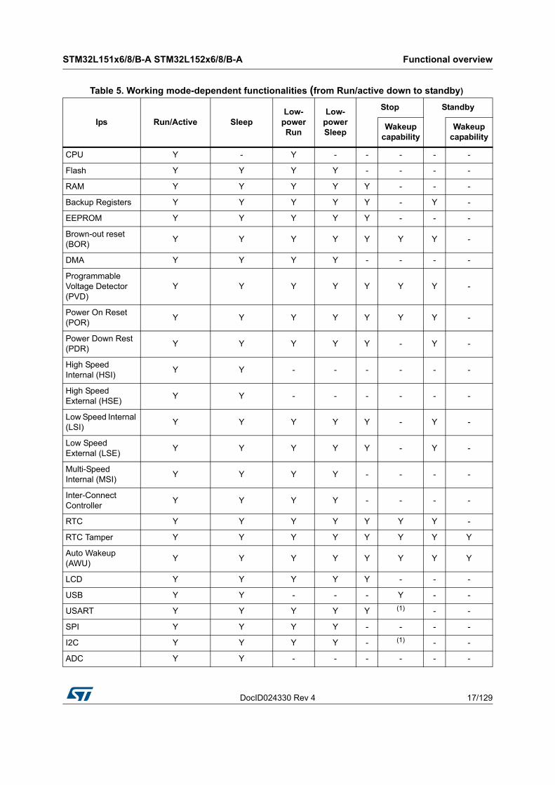
Table 5. Working mode-dependent functionalities (from Run/active down to standby)
Ips Run/Active SleepLow-
power Run
Low-power Sleep
Stop Standby
Wakeup capability
Wakeup capability
CPU Y - Y - - - - -
Flash Y Y Y Y - - - -
RAM Y Y Y Y Y - - -
Backup Registers Y Y Y Y Y - Y -
EEPROM Y Y Y Y Y - - -
Brown-out reset (BOR)
Y Y Y Y Y Y Y -
DMA Y Y Y Y - - - -
Programmable Voltage Detector (PVD)
Y Y Y Y Y Y Y -
Power On Reset (POR)
Y Y Y Y Y Y Y -
Power Down Rest (PDR)
Y Y Y Y Y - Y -
High Speed Internal (HSI)
Y Y - - - - - -
High Speed External (HSE)
Y Y - - - - - -
Low Speed Internal (LSI)
Y Y Y Y Y - Y -
Low Speed External (LSE)
Y Y Y Y Y - Y -
Multi-Speed Internal (MSI)
Y Y Y Y - - - -
Inter-Connect Controller
Y Y Y Y - - - -
RTC Y Y Y Y Y Y Y -
RTC Tamper Y Y Y Y Y Y Y Y
Auto Wakeup (AWU)
Y Y Y Y Y Y Y Y
LCD Y Y Y Y Y - - -
USB Y Y - - - Y - -
USART Y Y Y Y Y (1) - -
SPI Y Y Y Y - - - -
I2C Y Y Y Y - (1) - -
ADC Y Y - - - - - -
Functional overview STM32L151x6/8/B-A STM32L152x6/8/B-A
18/129 DocID024330 Rev 4
3.2 ARM® Cortex®-M3 core with MPU
The ARM® Cortex®-M3 processor is the industry leading processor for embedded systems. It has been developed to provide a low-cost platform that meets the needs of MCU implementation, with a reduced pin count and low-power consumption, while delivering outstanding computational performance and an advanced system response to interrupts.
The ARM® Cortex®-M3 32-bit RISC processor features exceptional code-efficiency, delivering the high-performance expected from an ARM core in the memory size usually associated with 8- and 16-bit devices.
The memory protection unit (MPU) improves system reliability by defining the memory attributes (such as read/write access permissions) for different memory regions. It provides up to eight different regions and an optional predefined background region.
Owing to its embedded ARM core, the STM32L151x6/8/B-A and STM32L152x6/8/B-A devices are compatible with all ARM tools and software.
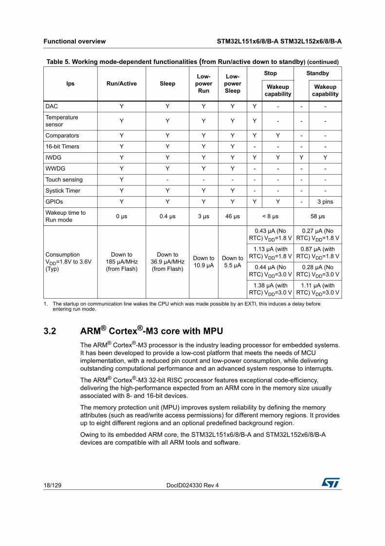
DAC Y Y Y Y Y - - -
Temperature sensor
Y Y Y Y Y - - -
Comparators Y Y Y Y Y Y - -
16-bit Timers Y Y Y Y - - - -
IWDG Y Y Y Y Y Y Y Y
WWDG Y Y Y Y - - - -
Touch sensing Y - - - - - - -
Systick Timer Y Y Y Y - - - -
GPIOs Y Y Y Y Y Y - 3 pins
Wakeup time to Run mode
0 µs 0.4 µs 3 µs 46 µs < 8 µs 58 µs
Consumption VDD=1.8V to 3.6V (Typ)
Down to 185 µA/MHz (from Flash)
Down to 36.9 µA/MHz (from Flash)
Down to 10.9 µA
Down to 5.5 µA
0.43 µA (No RTC) VDD=1.8 V
0.27 µA (No RTC) VDD=1.8 V
1.13 µA (with RTC) VDD=1.8 V
0.87 µA (with RTC) VDD=1.8 V
0.44 µA (No RTC) VDD=3.0 V
0.28 µA (No RTC) VDD=3.0 V
1.38 µA (with RTC) VDD=3.0 V
1.11 µA (with RTC) VDD=3.0 V
1. The startup on communication line wakes the CPU which was made possible by an EXTI, this induces a delay before entering run mode.
Table 5. Working mode-dependent functionalities (from Run/active down to standby) (continued)
Ips Run/Active SleepLow-
power Run
Low-power Sleep
Stop Standby
Wakeup capability
Wakeup capability
DocID024330 Rev 4 19/129
STM32L151x6/8/B-A STM32L152x6/8/B-A Functional overview
51
Nested vectored interrupt controller (NVIC)
The ultra-low-power STM32L151x6/8/B-A and STM32L152x6/8/B-A devices embed a nested vectored interrupt controller able to handle up to 45 maskable interrupt channels (not including the 16 interrupt lines of Cortex-M3) and 16 priority levels.
• Closely coupled NVIC gives low-latency interrupt processing
• Interrupt entry vector table address passed directly to the core
• Closely coupled NVIC core interface
• Allows early processing of interrupts
• Processing of late arriving, higher-priority interrupts
• Support for tail-chaining
• Processor state automatically saved
• Interrupt entry restored on interrupt exit with no instruction overhead
This hardware block provides flexible interrupt management features with minimal interrupt latency.
3.3 Reset and supply management
3.3.1 Power supply schemes
• VDD = 1.65 to 3.6 V: external power supply for I/Os and the internal regulator. Provided externally through VDD pins.
• VSSA, VDDA = 1.65 to 3.6 V: external analog power supplies for ADC, reset blocks, RCs and PLL (minimum voltage to be applied to VDDA is 1.8 V when the ADC is used). VDDA and VSSA must be connected to VDD and VSS, respectively.
3.3.2 Power supply supervisor
The device has an integrated ZEROPOWER power-on reset (POR)/power-down reset (PDR) that can be coupled with a brownout reset (BOR) circuitry.
The device exists in two versions:
• The version with BOR activated at power-on operates between 1.8 V and 3.6 V.
• The other version without BOR operates between 1.65 V and 3.6 V.
After the VDD threshold is reached (1.65 V or 1.8 V depending on the BOR which is active or not at power-on), the option byte loading process starts, either to confirm or modify default thresholds, or to disable the BOR permanently: in this case, the VDD min value becomes 1.65 V (whatever the version, BOR active or not, at power-on).
When BOR is active at power-on, it ensures proper operation starting from 1.8 V whatever the power ramp-up phase before it reaches 1.8 V. When BOR is not active at power-up, the power ramp-up should guarantee that 1.65 V is reached on VDD at least 1 ms after it exits the POR area.
Functional overview STM32L151x6/8/B-A STM32L152x6/8/B-A
20/129 DocID024330 Rev 4
Five BOR thresholds are available through option bytes, starting from 1.8 V to 3 V. To reduce the power consumption in Stop mode, it is possible to automatically switch off the internal reference voltage (VREFINT) in Stop mode. The device remains in reset mode when VDD is below a specified threshold, VPOR/PDR or VBOR, without the need for any external reset circuit.
Note: The start-up time at power-on is typically 3.3 ms when BOR is active at power-up, the start-up time at power-on can be decreased down to 1 ms typically for devices with BOR inactive at power-up.
The device features an embedded programmable voltage detector (PVD) that monitors the VDD/VDDA power supply and compares it to the VPVD threshold. This PVD offers 7 different levels between 1.85 V and 3.05 V, chosen by software, with a step around 200 mV. An interrupt can be generated when VDD/VDDA drops below the VPVD threshold and/or when VDD/VDDA is higher than the VPVD threshold. The interrupt service routine can then generate a warning message and/or put the MCU into a safe state. The PVD is enabled by software.
3.3.3 Voltage regulator
The regulator has three operation modes: main (MR), low-power (LPR) and power down.
• MR is used in Run mode (nominal regulation)
• LPR is used in the Low-power run, Low-power sleep and Stop modes
• Power down is used in Standby mode. The regulator output is high impedance, the kernel circuitry is powered down, inducing zero consumption but the contents of the registers and RAM are lost are lost except for the standby circuitry (wakeup logic, IWDG, RTC, LSI, LSE crystal 32K osc, RCC_CSR).
3.3.4 Boot modes
At startup, boot pins are used to select one of three boot options:
• Boot from Flash memory
• Boot from System Memory
• Boot from embedded RAM
The boot loader is located in System Memory. It is used to reprogram the Flash memory by using USART1 or USART2. See the application note “STM32 microcontroller system memory boot mode” (AN2606) for details.
DocID024330 Rev 4 21/129
STM32L151x6/8/B-A STM32L152x6/8/B-A Functional overview
51
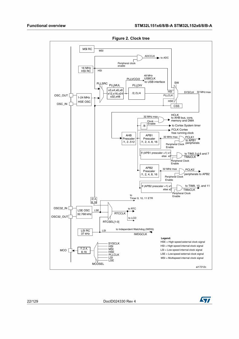
3.4 Clock management
The clock controller distributes the clocks coming from different oscillators to the core and the peripherals. It also manages clock gating for low-power modes and ensures clock robustness. It features:
• Clock prescaler: to get the best trade-off between speed and current consumption, the clock frequency to the CPU and peripherals can be adjusted by a programmable prescaler
• Safe clock switching: clock sources can be changed safely on the fly in run mode through a configuration register.
• Clock management: to reduce power consumption, the clock controller can stop the clock to the core, individual peripherals or memory.
• Master clock source: three different clock sources can be used to drive the master clock:
– 1-24 MHz high-speed external crystal (HSE), that can supply a PLL
– 16 MHz high-speed internal RC oscillator (HSI), trimmable by software, that can supply a PLL
– Multispeed internal RC oscillator (MSI), trimmable by software, able to generate 7 frequencies (65.5 kHz, 131 kHz, 262 kHz, 524 kHz, 1.05 MHz, 2.1 MHz, 4.2 MHz) with a consumption proportional to speed, down to 750 nA typical. When a 32.768 kHz clock source is available in the system (LSE), the MSI frequency can be trimmed by software down to a ±0.5% accuracy.
• Auxiliary clock source: two ultra-low-power clock sources that can be used to drive the LCD controller and the real-time clock:
– 32.768 kHz low-speed external crystal (LSE)
– 37 kHz low-speed internal RC (LSI), also used to drive the independent watchdog. The LSI clock can be measured using the high-speed internal RC oscillator for greater precision.
• RTC and LCD clock sources: the LSI, LSE or HSE sources can be chosen to clock the RTC and the LCD, whatever the system clock.
• USB clock source: the embedded PLL has a dedicated 48 MHz clock output to supply the USB interface.
• Startup clock: after reset, the microcontroller restarts by default with an internal 2.1 MHz clock (MSI). The prescaler ratio and clock source can be changed by the application program as soon as the code execution starts.
• Clock security system (CSS): this feature can be enabled by software. If a HSE clock failure occurs, the master clock is automatically switched to HSI and a software interrupt is generated if enabled.
• Clock-out capability (MCO: microcontroller clock output): it outputs one of the internal clocks for external use by the application.
Several prescalers allow the configuration of the AHB frequency, the high-speed APB (APB2) and the low-speed APB (APB1) domains. The maximum frequency of the AHB and the APB domains is 32 MHz. See Figure 2 for details on the clock tree.
Functional overview STM32L151x6/8/B-A STM32L152x6/8/B-A
22/129 DocID024330 Rev 4
Figure 2. Clock tree
DocID024330 Rev 4 23/129
STM32L151x6/8/B-A STM32L152x6/8/B-A Functional overview
51
3.5 Low-power real-time clock and backup registers
The real-time clock (RTC) is an independent BCD timer/counter. Dedicated registers contain the sub-second, second, minute, hour (12/24 hour), week day, date, month, year, in BCD (binary-coded decimal) format. Correction for 28, 29 (leap year), 30, and 31 day of the month are made automatically. The RTC provides two programmable alarms and programmable periodic interrupts with wakeup from Stop and Standby modes.
The programmable wakeup time ranges from 120 µs to 36 hours.
The RTC can be calibrated with an external 512 Hz output, and a digital compensation circuit helps reduce drift due to crystal deviation. The RTC can also be automatically corrected with a 50/60Hz stable power line.
The RTC calendar can be updated on the fly down to sub second precision, which enables network system synchronization. A time stamp can record an external event occurrence, and generates an interrupt.
There are twenty 32-bit backup registers provided to store 80 bytes of user application data. They are cleared in case of tamper detection. Three pins can be used to detect tamper events. A change on one of these pins can reset backup register and generate an interrupt. To prevent false tamper event, like ESD event, these three tamper inputs can be digitally filtered.
3.6 GPIOs (general-purpose inputs/outputs)
Each of the GPIO pins can be configured by software as output (push-pull or open-drain), as input (with or without pull-up or pull-down) or as peripheral alternate function. Most of the GPIO pins are shared with digital or analog alternate functions, and can be individually remapped using dedicated AFIO registers. All GPIOs are high current capable. The alternate function configuration of I/Os can be locked if needed following a specific sequence in order to avoid spurious writing to the I/O registers. The I/O controller is connected to the AHB with a toggling speed of up to 16 MHz.
External interrupt/event controller (EXTI)
The external interrupt/event controller consists of 23 edge detector lines used to generate interrupt/event requests. Each line can be individually configured to select the trigger event (rising edge, falling edge, both) and can be masked independently. A pending register maintains the status of the interrupt requests. The EXTI can detect an external line with a pulse width shorter than the Internal APB2 clock period. Up to 83 GPIOs can be connected to the 16 external interrupt lines. The 7 other lines are connected to RTC, PVD, USB or Comparator events.
Functional overview STM32L151x6/8/B-A STM32L152x6/8/B-A
24/129 DocID024330 Rev 4
3.7 Memories
The STM32L151x6/8/B-A and STM32L152x6/8/B-A devices have the following features:
• Up to 32 Kbytes of embedded RAM accessed (read/write) at CPU clock speed with 0 wait states. With the enhanced bus matrix, operating the RAM does not lead to any performance penalty during accesses to the system bus (AHB and APB buses).
• The non-volatile memory is divided into three arrays:
– 32, 64 or 128 Kbyte of embedded Flash program memory
– 4 Kbytes of data EEPROM
– Options bytes
The options bytes are used to write-protect or read-out-protect the memory (with 4 KB granularity) and/or readout-protect the whole memory with the following options:
– Level 0: no readout protection
– Level 1: memory readout protection, the Flash memory cannot be read from or written to if either debug features are connected or boot in RAM is selected
– Level 2: chip readout protection, debug features (Cortex-M3 JTAG and serial wire) and boot in RAM selection disabled (JTAG fuse)
The whole non-volatile memory embeds the error correction code (ECC) feature.
The user area of the Flash memory can be protected against Dbus read access by the PCROP feature (see RM0038 for details).
3.8 DMA (direct memory access)
The flexible 7-channel, general-purpose DMA is able to manage memory-to-memory, peripheral-to-memory and memory-to-peripheral transfers. The DMA controller supports circular buffer management, avoiding the generation of interrupts when the controller reaches the end of the buffer.
Each channel is connected to dedicated hardware DMA requests, with software trigger support for each channel. Configuration is done by software and transfer sizes between source and destination are independent.
The DMA can be used with the main peripherals: SPI, I2C, USART, general-purpose timers and ADC.
DocID024330 Rev 4 25/129
STM32L151x6/8/B-A STM32L152x6/8/B-A Functional overview
51
3.9 LCD (liquid crystal display)
The LCD drives up to 8 common terminals and 44 segment terminals to drive up to 320 pixels.
• Internal step-up converter to guarantee functionality and contrast control irrespective of VDD. This converter can be deactivated, in which case the VLCD pin is used to provide the voltage to the LCD
• Supports static, 1/2, 1/3, 1/4 and 1/8 duty
• Supports static, 1/2, 1/3 and 1/4 bias
• Phase inversion to reduce power consumption and EMI
• Up to 8 pixels can be programmed to blink
• Unneeded segments and common pins can be used as general I/O pins
• LCD RAM can be updated at any time owing to a double-buffer
• The LCD controller can operate in Stop mode
• VLCD rail decoupling capability
3.10 ADC (analog-to-digital converter)
A 12-bit analog-to-digital converters is embedded into STM32L151x6/8/B-A and STM32L152x6/8/B-A devices with up to 24 external channels, performing conversions in single-shot or scan mode. In scan mode, automatic conversion is performed on a selected group of analog inputs.
The ADC can be served by the DMA controller.
An analog watchdog feature allows very precise monitoring of the converted voltage of one, some or all selected channels. An interrupt is generated when the converted voltage is outside the programmed thresholds.
The events generated by the general-purpose timers (TIMx) can be internally connected to the ADC start trigger and injection trigger, to allow the application to synchronize A/D conversions and timers. An injection mode allows high priority conversions to be done by interrupting a scan mode which runs in as a background task.
The ADC includes a specific low-power mode. The converter is able to operate at maximum speed even if the CPU is operating at a very low frequency and has an auto-shutdown function. The ADC’s runtime and analog front-end current consumption are thus minimized whatever the MCU operating mode.
Table 6. VLCD rail decoupling
BiasPin
1/2 1/3 1/4
VLCDrail1 1/2 VLCD 2/3 VLCD 1/2 VLCD PB2
VLCDrail2 NA 1/3 VLCD 1/4 VLCD PB12 PE11
VLCDrail3 NA NA 3/4 VLCD PB0 PE12
Functional overview STM32L151x6/8/B-A STM32L152x6/8/B-A
26/129 DocID024330 Rev 4
3.10.1 Temperature sensor
The temperature sensor TSENSE generates a voltage VSENSE that varies linearly with temperature.
The temperature sensor is internally connected to the ADC_IN16 input channel which is used to convert the sensor output voltage into a digital value.
The sensor provides good linearity but it has to be calibrated to obtain good overall accuracy of the temperature measurement. As the offset of the temperature sensor varies from chip to chip due to process variation, the uncalibrated internal temperature sensor is suitable for applications that detect temperature changes only.
To improve the accuracy of the temperature sensor measurement, each device is individually factory-calibrated by ST. The temperature sensor factory calibration data are stored by ST in the system memory area, accessible in read-only mode, see Table 59: Temperature sensor calibration values.
3.10.2 Internal voltage reference (VREFINT)
The internal voltage reference (VREFINT) provides a stable (bandgap) voltage output for the ADC and Comparators. VREFINT is internally connected to the ADC_IN17 input channel. It enables accurate monitoring of the VDD value (when no external voltage, VREF+, is available for ADC). The precise voltage of VREFINT is individually measured for each part by ST during production test and stored in the system memory area. It is accessible in read-only mode see Table 17: Embedded internal reference voltage.
3.11 DAC (digital-to-analog converter)
The two 12-bit buffered DAC channels can be used to convert two digital signals into two analog voltage signal outputs. The chosen design structure is composed of integrated resistor strings and an amplifier in non-inverting configuration.
This dual digital Interface supports the following features:
• two DAC converters: one for each output channel
• left or right data alignment in 12-bit mode
• synchronized update capability
• noise-wave generation
• triangular-wave generation
• dual DAC channels’ independent or simultaneous conversions
• DMA capability for each channel (including the underrun interrupt)
• external triggers for conversion
• input reference voltage VREF+
Eight DAC trigger inputs are used in the STM32L151x6/8/B-A and STM32L152x6/8/B-A devices. The DAC channels are triggered through the timer update outputs that are also connected to different DMA channels.
DocID024330 Rev 4 27/129
STM32L151x6/8/B-A STM32L152x6/8/B-A Functional overview
51
3.12 Ultra-low-power comparators and reference voltage
The STM32L151x6/8/B-A and STM32L152x6/8/B-A devices embed two comparators sharing the same current bias and reference voltage. The reference voltage can be internal or external (coming from an I/O).
• one comparator with fixed threshold
• one comparator with rail-to-rail inputs, fast or slow mode. The threshold can be one of the following:
– DAC output
– External I/O
– Internal reference voltage (VREFINT) or VREFINT submultiple (1/4, 1/2, 3/4)
Both comparators can wake up from Stop mode, and be combined into a window comparator.
The internal reference voltage is available externally via a low-power / low-current output buffer (driving current capability of 1 µA typical).
3.13 Routing interface
The highly flexible routing interface allows the application firmware to control the routing of different I/Os to the TIM2, TIM3 and TIM4 timer input captures. It also controls the routing of internal analog signals to ADC1, COMP1 and COMP2 and the internal reference voltage VREFINT.
3.14 Touch sensing
The STM32L151x6/8/B-A and STM32L152x6/8/B-A devices provide a simple solution for adding capacitive sensing functionality to any application. These devices offer up to 20 capacitive sensing channels distributed over 10 analog I/O groups. Both software and timer capacitive sensing acquisition modes are supported.
Capacitive sensing technology is able to detect the presence of a finger near a sensor which is protected from direct touch by a dielectric (glass, plastic, ...). The capacitive variation introduced by the finger (or any conductive object) is measured using a proven implementation based on a surface charge transfer acquisition principle. It consists of charging the sensor capacitance and then transferring a part of the accumulated charges into a sampling capacitor until the voltage across this capacitor has reached a specific threshold. The capacitive sensing acquisition only requires few external components to operate. This acquisition is managed directly by the GPIOs, timers and analog I/O groups (see Section 3.13: Routing interface).
Reliable touch sensing functionality can be quickly and easily implemented using the free STM32L1xx STMTouch touch sensing firmware library.
3.15 Timers and watchdogs
The ultra-low-power STM32L151x6/8/B-A and STM32L152x6/8/B-A devices include six general-purpose timers, two basic timers and two watchdog timers.
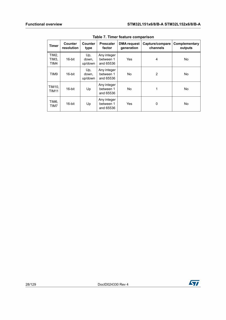
Table 7 compares the features of the general-purpose and basic timers.
Functional overview STM32L151x6/8/B-A STM32L152x6/8/B-A
28/129 DocID024330 Rev 4
Table 7. Timer feature comparison
TimerCounter
resolutionCounter
typePrescaler
factorDMA request generation
Capture/compare channels
Complementaryoutputs
TIM2, TIM3, TIM4
16-bitUp,
down, up/down
Any integer between 1 and 65536
Yes 4 No
TIM9 16-bitUp,
down, up/down
Any integer between 1 and 65536
No 2 No
TIM10, TIM11
16-bit UpAny integer between 1 and 65536
No 1 No
TIM6, TIM7
16-bit UpAny integer between 1 and 65536
Yes 0 No
DocID024330 Rev 4 29/129
STM32L151x6/8/B-A STM32L152x6/8/B-A Functional overview
51
3.15.1 General-purpose timers (TIM2, TIM3, TIM4, TIM9, TIM10 and TIM11)
There are six synchronizable general-purpose timers embedded in the STM32L151x6/8/B-A and STM32L152x6/8/B-A devices (see Table 7 for differences).
TIM2, TIM3, TIM4
These timers are based on a 16-bit auto-reload up/down-counter and a 16-bit prescaler. They feature 4 independent channels each for input capture/output compare, PWM or one-pulse mode output. This gives up to 12 input captures/output compares/PWMs on the largest packages.
The TIM2, TIM3, TIM4 general-purpose timers can work together or with the TIM10, TIM11 and TIM9 general-purpose timers via the Timer Link feature for synchronization or event chaining. Their counter can be frozen in debug mode. Any of the general-purpose timers can be used to generate PWM outputs.
TIM2, TIM3, TIM4 all have independent DMA request generation.
These timers are capable of handling quadrature (incremental) encoder signals and the digital outputs from 1 to 3 hall-effect sensors.
TIM10, TIM11 and TIM9
TIM10 and TIM11 are based on a 16-bit auto-reload upcounter. TIM9 is based on a 16-bit auto-reload up/down counter. They include a 16-bit prescaler. TIM10 and TIM11 feature one independent channel, whereas TIM9 has two independent channels for input capture/output compare, PWM or one-pulse mode output. They can be synchronized with the TIM2, TIM3, TIM4 full-featured general-purpose timers.
They can also be used as simple time bases and be clocked by the LSE clock source (32.768 kHz) to provide time bases independent from the main CPU clock.
3.15.2 Basic timers (TIM6 and TIM7)
These timers are mainly used for DAC trigger generation. They can also be used as generic 16-bit time bases.
3.15.3 SysTick timer
This timer is dedicated to the OS, but could also be used as a standard downcounter. It is based on a 24-bit down-counter with autoreload capability and a programmable clock source. It features a maskable system interrupt generation when the counter reaches 0.
3.15.4 Independent watchdog (IWDG)
The independent watchdog is based on a 12-bit down-counter and 8-bit prescaler. It is clocked from an independent 37 kHz internal RC and, as it operates independently of the main clock, it can operate in Stop and Standby modes. It can be used either as a watchdog to reset the device when a problem occurs, or as a free-running timer for application timeout management. It is hardware- or software-configurable through the option bytes. The counter can be frozen in debug mode.
Functional overview STM32L151x6/8/B-A STM32L152x6/8/B-A
30/129 DocID024330 Rev 4
3.15.5 Window watchdog (WWDG)
The window watchdog is based on a 7-bit down-counter that can be set as free-running. It can be used as a watchdog to reset the device when a problem occurs. It is clocked from the main clock. It has an early warning interrupt capability and the counter can be frozen in debug mode.
3.16 Communication interfaces
3.16.1 I²C bus
Up to two I²C bus interfaces can operate in multimaster and slave modes. They can support standard and fast modes.
They support dual slave addressing (7-bit only) and both 7- and 10-bit addressing in master mode. A hardware CRC generation/verification is embedded.
They can be served by DMA and they support SM Bus 2.0/PM Bus.
3.16.2 Universal synchronous/asynchronous receiver transmitter (USART)
All USART interfaces are able to communicate at speeds of up to 4 Mbit/s. They provide hardware management of the CTS and RTS signals and are ISO 7816 compliant. They support IrDA SIR ENDEC and have LIN Master/Slave capability.
All USART interfaces can be served by the DMA controller.
3.16.3 Serial peripheral interface (SPI)
Up to two SPIs are able to communicate at up to 16 Mbits/s in slave and master modes in full-duplex and half-duplex communication modes. The 3-bit prescaler gives 8 master mode frequencies and the frame is configurable to 8 bits or 16 bits. The hardware CRC generation/verification supports basic SD Card/MMC modes.
Both SPIs can be served by the DMA controller.
3.16.4 Universal serial bus (USB)
The STM32L151x6/8/B-A and STM32L152x6/8/B-A devices embed a USB device peripheral compatible with the USB full speed 12 Mbit/s. The USB interface implements a full speed (12 Mbit/s) function interface. It has software-configurable endpoint setting and supports suspend/resume. The dedicated 48 MHz clock is generated from the internal main PLL (the clock source must use a HSE crystal oscillator).
DocID024330 Rev 4 31/129
STM32L151x6/8/B-A STM32L152x6/8/B-A Functional overview
51
3.17 CRC (cyclic redundancy check) calculation unit
The CRC (cyclic redundancy check) calculation unit is used to get a CRC code from a 32-bit data word and a fixed generator polynomial.
Among other applications, CRC-based techniques are used to verify data transmission or storage integrity. In the scope of the EN/IEC 60335-1 standard, they offer a means of verifying the Flash memory integrity. The CRC calculation unit helps compute a signature of the software during runtime, to be compared with a reference signature generated at link-time and stored at a given memory location.
3.18 Development support
Serial wire JTAG debug port (SWJ-DP)
The ARM SWJ-DP interface is embedded, and is a combined JTAG and serial wire debug port that enables either a serial wire debug or a JTAG probe to be connected to the target. The JTAG JTMS and JTCK pins are shared with SWDAT and SWCLK, respectively, and a specific sequence on the JTMS pin is used to switch between JTAG-DP and SW-DP.
The JTAG port can be permanently disabled with a JTAG fuse.
Embedded Trace Macrocell™
The ARM Embedded Trace Macrocell provides a greater visibility of the instruction and data flow inside the CPU core by streaming compressed data at a very high rate from the STM32L151x6/8/B-A and STM32L152x6/8/B-A device through a small number of ETM pins to an external hardware trace port analyzer (TPA) device. The TPA is connected to a host computer using USB, Ethernet, or any other high-speed channel. Real-time instruction and data flow activity can be recorded and then formatted for display on the host computer running debugger software. TPA hardware is commercially available from common development tool vendors. It operates with third party debugger software tools.
Pin descriptions STM32L151x6/8/B-A STM32L152x6/8/B-A
32/129 DocID024330 Rev 4
4 Pin descriptions
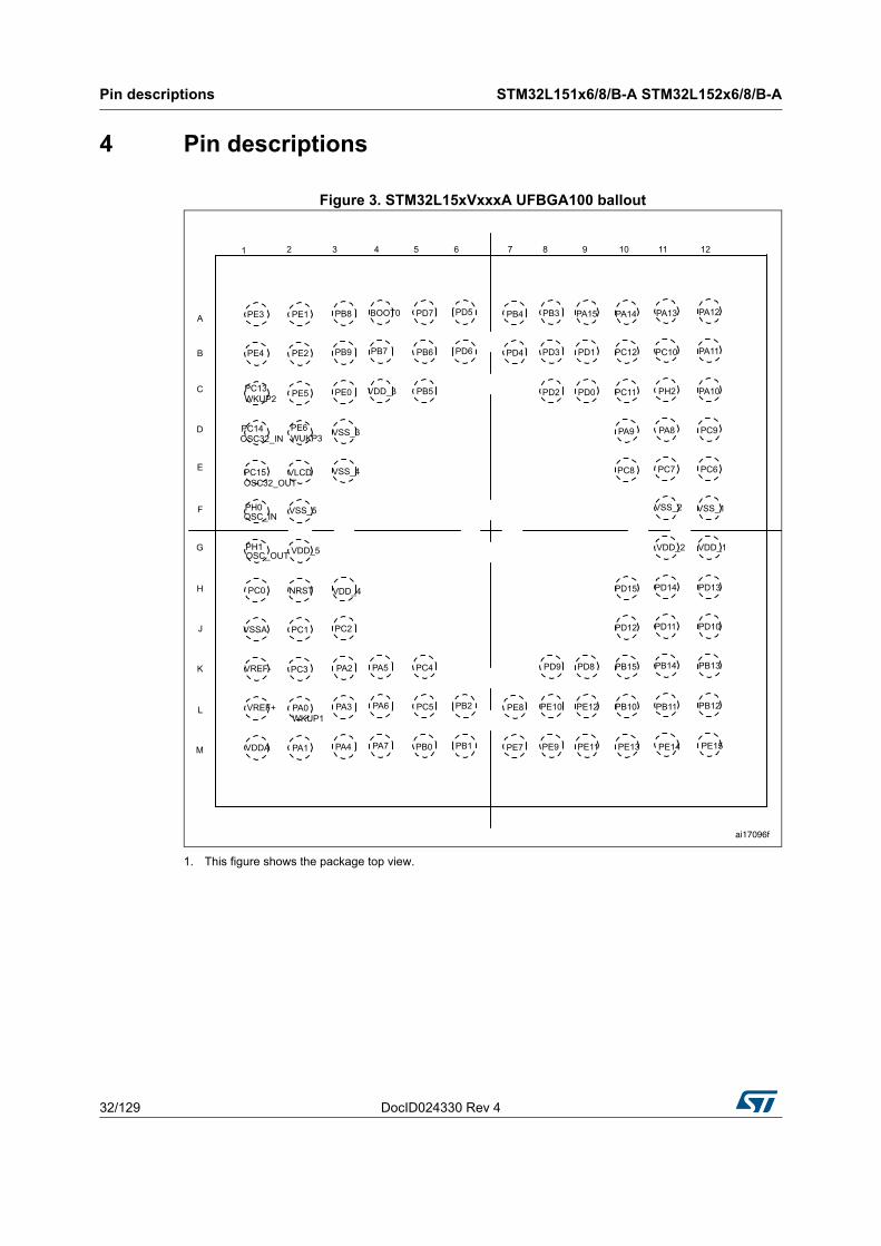
Figure 3. STM32L15xVxxxA UFBGA100 ballout
1. This figure shows the package top view.
DocID024330 Rev 4 33/129
STM32L151x6/8/B-A STM32L152x6/8/B-A Pin descriptions
51
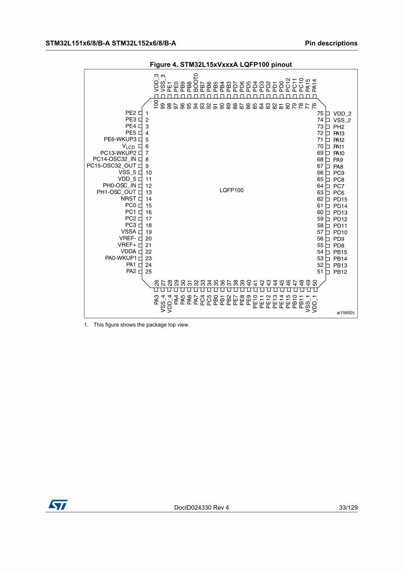
Figure 4. STM32L15xVxxxA LQFP100 pinout
1. This figure shows the package top view.
Pin descriptions STM32L151x6/8/B-A STM32L152x6/8/B-A
34/129 DocID024330 Rev 4
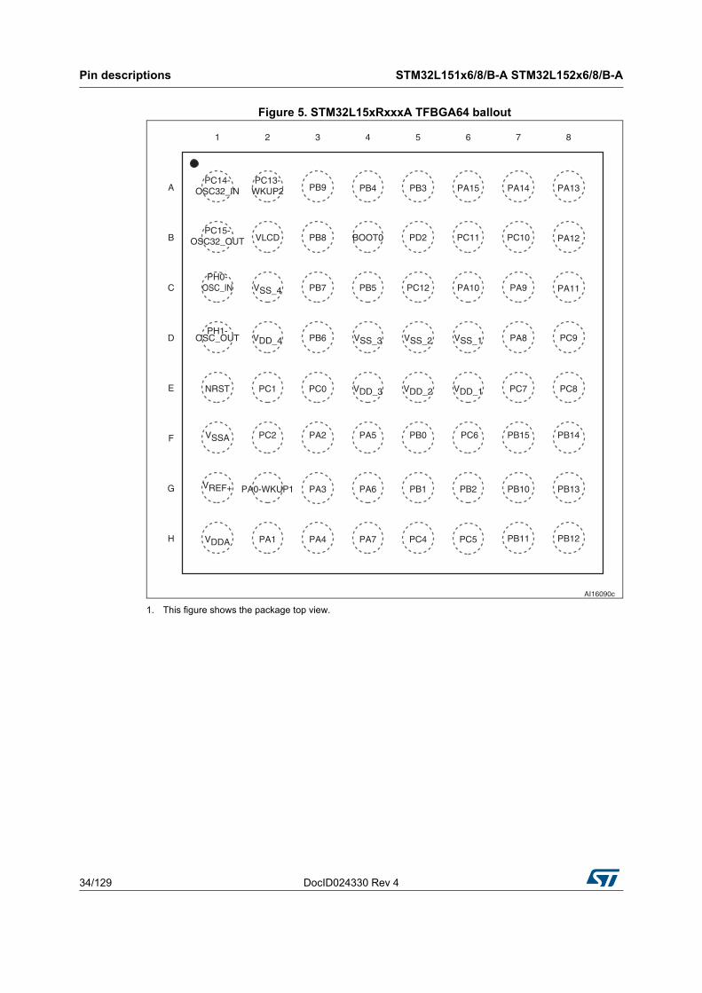
Figure 5. STM32L15xRxxxA TFBGA64 ballout
1. This figure shows the package top view.
AI16090c
PB2
PC14-OSC32_IN
PA7PA4
PA2
PA15
PB11
PB1PA6PA3
H
PB10
PC5PC4
D PA8
PA9
BOOT0PB8
C
PC9
PA11
PB6
PC12
VDDA
PB9
B PA12PC10PC15-
OSC32_OUT
PB3
PD2
A
87654321
VSS_4OSC_IN
OSC_OUT VDD_4
G
F
E
PC2
VREF+
PC13-WKUP2 PB4 PA13PA14
PB7 PB5
VSS_3
PC7 PC8PC0NRST PC1
PB0PA5 PB14
VDD_2VDD_3
PB13
VLCD PC11
PA10
VSS_2 VSS_1
PC6VSSA
PA1
VDD_1
PB15
PB12
PA0-WKUP1
PH0-
PH1-
DocID024330 Rev 4 35/129
STM32L151x6/8/B-A STM32L152x6/8/B-A Pin descriptions
51
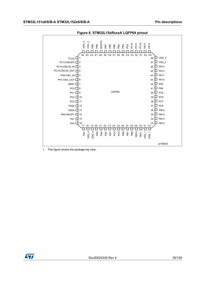
Figure 6. STM32L15xRxxxA LQFP64 pinout
1. This figure shows the package top view.
Pin descriptions STM32L151x6/8/B-A STM32L152x6/8/B-A
36/129 DocID024330 Rev 4
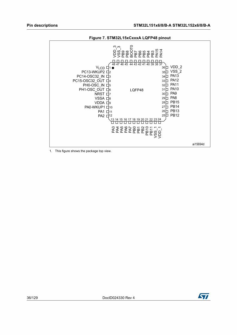
Figure 7. STM32L15xCxxxA LQFP48 pinout
1. This figure shows the package top view.
DocID024330 Rev 4 37/129
STM32L151x6/8/B-A STM32L152x6/8/B-A Pin descriptions
51
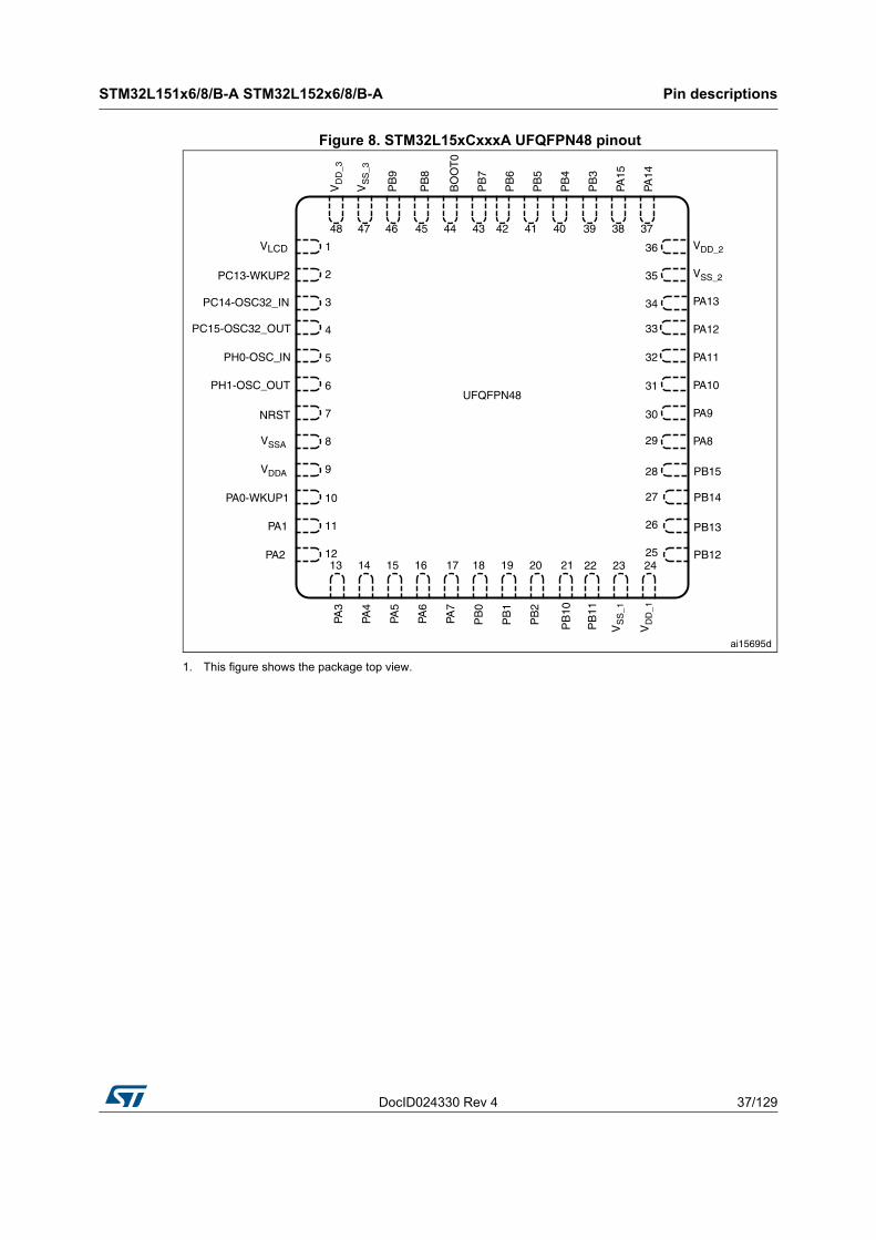
Figure 8. STM32L15xCxxxA UFQFPN48 pinout
1. This figure shows the package top view.
Pin descriptions STM32L151x6/8/B-A STM32L152x6/8/B-A
38/129 DocID024330 Rev 4
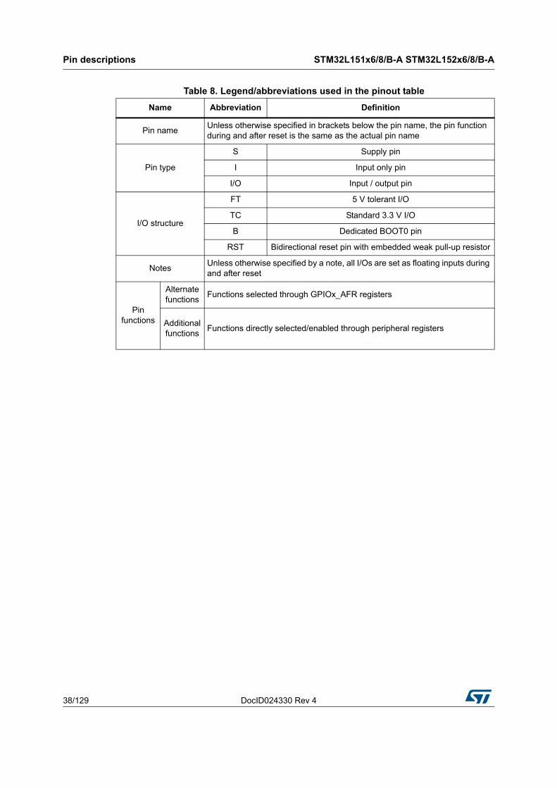
Table 8. Legend/abbreviations used in the pinout table
Name Abbreviation Definition
Pin nameUnless otherwise specified in brackets below the pin name, the pin function during and after reset is the same as the actual pin name
Pin type
S Supply pin
I Input only pin
I/O Input / output pin
I/O structure
FT 5 V tolerant I/O
TC Standard 3.3 V I/O
B Dedicated BOOT0 pin
RST Bidirectional reset pin with embedded weak pull-up resistor
NotesUnless otherwise specified by a note, all I/Os are set as floating inputs during and after reset
Pin functions
Alternate functions
Functions selected through GPIOx_AFR registers
Additional functions
Functions directly selected/enabled through peripheral registers
DocID024330 Rev 4 39/129
STM32L151x6/8/B-A STM32L152x6/8/B-A Pin descriptions
51
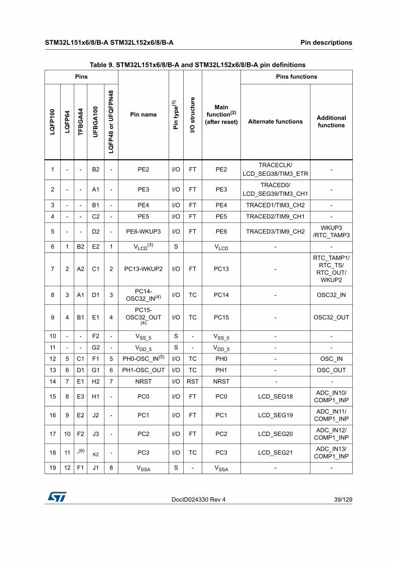
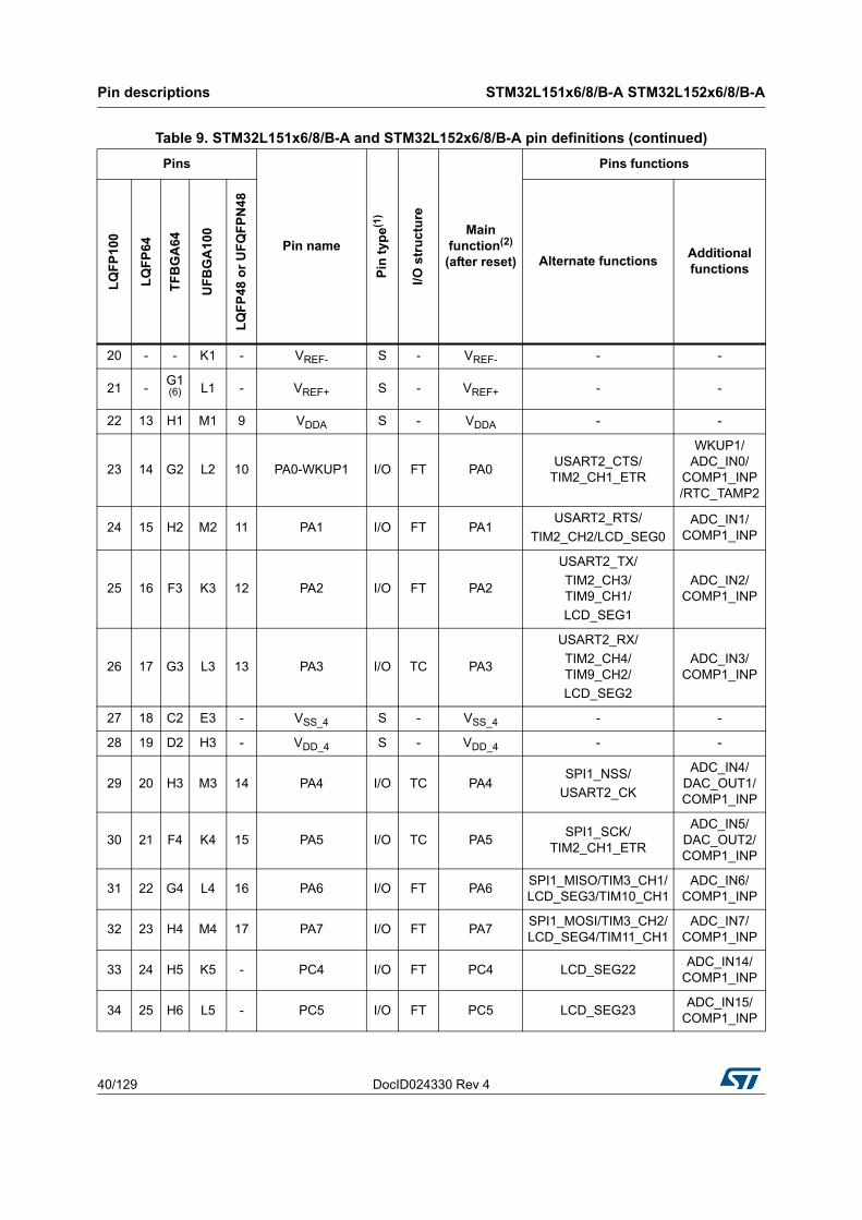
Table 9. STM32L151x6/8/B-A and STM32L152x6/8/B-A pin definitions
Pins
Pin name
Pin
typ
e(1)
I/O s
tru
ctu
re
Main function(2)
(after reset)
Pins functions
LQ
FP
100
LQ
FP
64
TF
BG
A6
4
UF
BG
A10
0
LQ
FP
48
or
UF
QF
PN
48
Alternate functionsAdditional functions
1 - - B2 - PE2 I/O FT PE2TRACECLK/
LCD_SEG38/TIM3_ETR-
2 - - A1 - PE3 I/O FT PE3TRACED0/
LCD_SEG39/TIM3_CH1-
3 - - B1 - PE4 I/O FT PE4 TRACED1/TIM3_CH2 -
4 - - C2 - PE5 I/O FT PE5 TRACED2/TIM9_CH1 -
5 - - D2 - PE6-WKUP3 I/O FT PE6 TRACED3/TIM9_CH2WKUP3
/RTC_TAMP3
6 1 B2 E2 1 VLCD(3) S VLCD - -
7 2 A2 C1 2 PC13-WKUP2 I/O FT PC13 -
RTC_TAMP1/ RTC_TS/
RTC_OUT/ WKUP2
8 3 A1 D1 3PC14-
OSC32_IN(4) I/O TC PC14 - OSC32_IN
9 4 B1 E1 4PC15-
OSC32_OUT(4)
I/O TC PC15 - OSC32_OUT
10 - - F2 - VSS_5 S - VSS_5 - -
11 - - G2 - VDD_5 S - VDD_5 - -
12 5 C1 F1 5 PH0-OSC_IN(5) I/O TC PH0 - OSC_IN
13 6 D1 G1 6 PH1-OSC_OUT I/O TC PH1 - OSC_OUT
14 7 E1 H2 7 NRST I/O RST NRST - -
15 8 E3 H1 - PC0 I/O FT PC0 LCD_SEG18ADC_IN10/
COMP1_INP
16 9 E2 J2 - PC1 I/O FT PC1 LCD_SEG19ADC_IN11/
COMP1_INP
17 10 F2 J3 - PC2 I/O FT PC2 LCD_SEG20ADC_IN12/
COMP1_INP
18 11 -(6)K2 - PC3 I/O TC PC3 LCD_SEG21
ADC_IN13/ COMP1_INP
19 12 F1 J1 8 VSSA S - VSSA - -
Pin descriptions STM32L151x6/8/B-A STM32L152x6/8/B-A
40/129 DocID024330 Rev 4
20 - - K1 - VREF- S - VREF- - -
21 -G1(6) L1 - VREF+ S - VREF+ - -
22 13 H1 M1 9 VDDA S - VDDA - -
23 14 G2 L2 10 PA0-WKUP1 I/O FT PA0USART2_CTS/
TIM2_CH1_ETR
WKUP1/ ADC_IN0/
COMP1_INP /RTC_TAMP2
24 15 H2 M2 11 PA1 I/O FT PA1USART2_RTS/
TIM2_CH2/LCD_SEG0ADC_IN1/
COMP1_INP
25 16 F3 K3 12 PA2 I/O FT PA2
USART2_TX/
TIM2_CH3/TIM9_CH1/
LCD_SEG1
ADC_IN2/ COMP1_INP
26 17 G3 L3 13 PA3 I/O TC PA3
USART2_RX/
TIM2_CH4/TIM9_CH2/
LCD_SEG2
ADC_IN3/ COMP1_INP
27 18 C2 E3 - VSS_4 S - VSS_4 - -
28 19 D2 H3 - VDD_4 S - VDD_4 - -
29 20 H3 M3 14 PA4 I/O TC PA4SPI1_NSS/
USART2_CK
ADC_IN4/ DAC_OUT1/ COMP1_INP
30 21 F4 K4 15 PA5 I/O TC PA5SPI1_SCK/
TIM2_CH1_ETR
ADC_IN5/DAC_OUT2/ COMP1_INP
31 22 G4 L4 16 PA6 I/O FT PA6SPI1_MISO/TIM3_CH1/LCD_SEG3/TIM10_CH1
ADC_IN6/ COMP1_INP
32 23 H4 M4 17 PA7 I/O FT PA7SPI1_MOSI/TIM3_CH2/LCD_SEG4/TIM11_CH1
ADC_IN7/ COMP1_INP
33 24 H5 K5 - PC4 I/O FT PC4 LCD_SEG22ADC_IN14/
COMP1_INP
34 25 H6 L5 - PC5 I/O FT PC5 LCD_SEG23ADC_IN15/
COMP1_INP
Table 9. STM32L151x6/8/B-A and STM32L152x6/8/B-A pin definitions (continued)
Pins
Pin name
Pin
typ
e(1)
I/O s
tru
ctu
re
Main function(2)
(after reset)
Pins functions
LQ
FP
100
LQ
FP
64
TF
BG
A64
UF
BG
A1
00
LQ
FP
48 o
r U
FQ
FP
N48
Alternate functionsAdditional functions
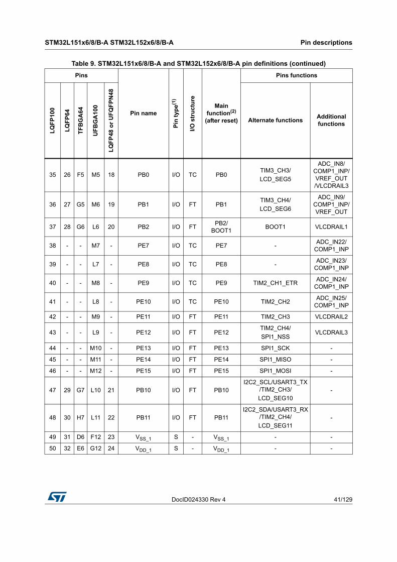
DocID024330 Rev 4 41/129
STM32L151x6/8/B-A STM32L152x6/8/B-A Pin descriptions
51
35 26 F5 M5 18 PB0 I/O TC PB0TIM3_CH3/
LCD_SEG5
ADC_IN8/COMP1_INP/ VREF_OUT /VLCDRAIL3
36 27 G5 M6 19 PB1 I/O FT PB1TIM3_CH4/
LCD_SEG6
ADC_IN9/COMP1_INP/ VREF_OUT
37 28 G6 L6 20 PB2 I/O FTPB2/
BOOT1BOOT1 VLCDRAIL1
38 - - M7 - PE7 I/O TC PE7 -ADC_IN22/
COMP1_INP
39 - - L7 - PE8 I/O TC PE8 -ADC_IN23/
COMP1_INP
40 - - M8 - PE9 I/O TC PE9 TIM2_CH1_ETRADC_IN24/
COMP1_INP
41 - - L8 - PE10 I/O TC PE10 TIM2_CH2ADC_IN25/
COMP1_INP
42 - - M9 - PE11 I/O FT PE11 TIM2_CH3 VLCDRAIL2
43 - - L9 - PE12 I/O FT PE12TIM2_CH4/
SPI1_NSSVLCDRAIL3
44 - - M10 - PE13 I/O FT PE13 SPI1_SCK -
45 - - M11 - PE14 I/O FT PE14 SPI1_MISO -
46 - - M12 - PE15 I/O FT PE15 SPI1_MOSI -
47 29 G7 L10 21 PB10 I/O FT PB10I2C2_SCL/USART3_TX
/TIM2_CH3/
LCD_SEG10-
48 30 H7 L11 22 PB11 I/O FT PB11I2C2_SDA/USART3_RX
/TIM2_CH4/
LCD_SEG11-
49 31 D6 F12 23 VSS_1 S - VSS_1 - -
50 32 E6 G12 24 VDD_1 S - VDD_1 - -
Table 9. STM32L151x6/8/B-A and STM32L152x6/8/B-A pin definitions (continued)
Pins
Pin name
Pin
typ
e(1)
I/O s
tru
ctu
re
Main function(2)
(after reset)
Pins functions
LQ
FP
100
LQ
FP
64
TF
BG
A64
UF
BG
A1
00
LQ
FP
48 o
r U
FQ
FP
N48
Alternate functionsAdditional functions
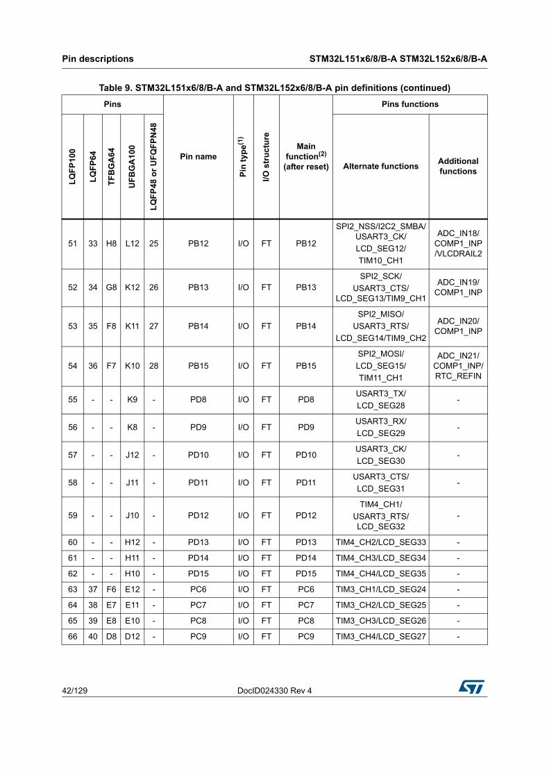
Pin descriptions STM32L151x6/8/B-A STM32L152x6/8/B-A
42/129 DocID024330 Rev 4
51 33 H8 L12 25 PB12 I/O FT PB12
SPI2_NSS/I2C2_SMBA/ USART3_CK/
LCD_SEG12/
TIM10_CH1
ADC_IN18/ COMP1_INP /VLCDRAIL2
52 34 G8 K12 26 PB13 I/O FT PB13SPI2_SCK/
USART3_CTS/ LCD_SEG13/TIM9_CH1
ADC_IN19/ COMP1_INP
53 35 F8 K11 27 PB14 I/O FT PB14
SPI2_MISO/
USART3_RTS/
LCD_SEG14/TIM9_CH2
ADC_IN20/ COMP1_INP
54 36 F7 K10 28 PB15 I/O FT PB15
SPI2_MOSI/
LCD_SEG15/
TIM11_CH1
ADC_IN21/ COMP1_INP/RTC_REFIN
55 - - K9 - PD8 I/O FT PD8USART3_TX/
LCD_SEG28-
56 - - K8 - PD9 I/O FT PD9USART3_RX/
LCD_SEG29-
57 - - J12 - PD10 I/O FT PD10USART3_CK/
LCD_SEG30-
58 - - J11 - PD11 I/O FT PD11USART3_CTS/
LCD_SEG31-
59 - - J10 - PD12 I/O FT PD12TIM4_CH1/
USART3_RTS/ LCD_SEG32
-
60 - - H12 - PD13 I/O FT PD13 TIM4_CH2/LCD_SEG33 -
61 - - H11 - PD14 I/O FT PD14 TIM4_CH3/LCD_SEG34 -
62 - - H10 - PD15 I/O FT PD15 TIM4_CH4/LCD_SEG35 -
63 37 F6 E12 - PC6 I/O FT PC6 TIM3_CH1/LCD_SEG24 -
64 38 E7 E11 - PC7 I/O FT PC7 TIM3_CH2/LCD_SEG25 -
65 39 E8 E10 - PC8 I/O FT PC8 TIM3_CH3/LCD_SEG26 -
66 40 D8 D12 - PC9 I/O FT PC9 TIM3_CH4/LCD_SEG27 -
Table 9. STM32L151x6/8/B-A and STM32L152x6/8/B-A pin definitions (continued)
Pins
Pin name
Pin
typ
e(1)
I/O s
tru
ctu
re
Main function(2)
(after reset)
Pins functions
LQ
FP
100
LQ
FP
64
TF
BG
A64
UF
BG
A1
00
LQ
FP
48 o
r U
FQ
FP
N48
Alternate functionsAdditional functions
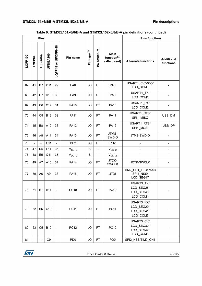
DocID024330 Rev 4 43/129
STM32L151x6/8/B-A STM32L152x6/8/B-A Pin descriptions
51
67 41 D7 D11 29 PA8 I/O FT PA8USART1_CK/MCO/
LCD_COM0-
68 42 C7 D10 30 PA9 I/O FT PA9USART1_TX/
LCD_COM1-
69 43 C6 C12 31 PA10 I/O FT PA10USART1_RX/
LCD_COM2-
70 44 C8 B12 32 PA11 I/O FT PA11USART1_CTS/
SPI1_MISOUSB_DM
71 45 B8 A12 33 PA12 I/O FT PA12USART1_RTS/
SPI1_MOSIUSB_DP
72 46 A8 A11 34 PA13 I/O FTJTMS-SWDIO
JTMS-SWDIO -
73 - - C11 - PH2 I/O FT PH2 - -
74 47 D5 F11 35 VSS_2 S - VSS_2 - -
75 48 E5 G11 36 VDD_2 S - VDD_2 - -
76 49 A7 A10 37 PA14 I/O FTJTCK-
SWCLKJCTK-SWCLK -
77 50 A6 A9 38 PA15 I/O FT JTDITIM2_CH1_ETR/PA15/
SPI1_NSS/LCD_SEG17
-
78 51 B7 B11 - PC10 I/O FT PC10
USART3_TX/
LCD_SEG28/
LCD_SEG40/
LCD_COM4
-
79 52 B6 C10 - PC11 I/O FT PC11
USART3_RX/
LCD_SEG29/
LCD_SEG41/
LCD_COM5
-
80 53 C5 B10 - PC12 I/O FT PC12
USART3_CK/
LCD_SEG30/
LCD_SEG42/LCD_COM6
-
81 - - C9 - PD0 I/O FT PD0 SPI2_NSS/TIM9_CH1 -
Table 9. STM32L151x6/8/B-A and STM32L152x6/8/B-A pin definitions (continued)
Pins
Pin name
Pin
typ
e(1)
I/O s
tru
ctu
re
Main function(2)
(after reset)
Pins functions
LQ
FP
100
LQ
FP
64
TF
BG
A64
UF
BG
A1
00
LQ
FP
48 o
r U
FQ
FP
N48
Alternate functionsAdditional functions
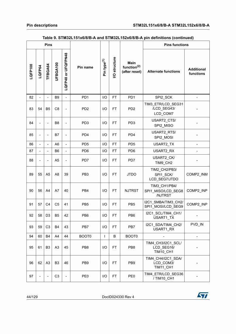
Pin descriptions STM32L151x6/8/B-A STM32L152x6/8/B-A
44/129 DocID024330 Rev 4
82 - - B9 - PD1 I/O FT PD1 SPI2_SCK -
83 54 B5 C8 - PD2 I/O FT PD2TIM3_ETR/LCD_SEG31
/LCD_SEG43/
LCD_COM7-
84 - - B8 - PD3 I/O FT PD3USART2_CTS/
SPI2_MISO-
85 - - B7 - PD4 I/O FT PD4USART2_RTS/
SPI2_MOSI-
86 - - A6 - PD5 I/O FT PD5 USART2_TX -
87 - - B6 - PD6 I/O FT PD6 USART2_RX -
88 - - A5 - PD7 I/O FT PD7USART2_CK/
TIM9_CH2-
89 55 A5 A8 39 PB3 I/O FT JTDOTIM2_CH2/PB3/
SPI1_SCK/LCD_SEG7/JTDO
COMP2_INM
90 56 A4 A7 40 PB4 I/O FT NJTRSTTIM3_CH1/PB4/
SPI1_MISO/LCD_SEG8/NJTRST
COMP2_INP
91 57 C4 C5 41 PB5 I/O FT PB5I2C1_SMBA/TIM3_CH2/ SPI1_MOSI/LCD_SEG9
COMP2_INP
92 58 D3 B5 42 PB6 I/O FT PB6I2C1_SCL/TIM4_CH1/
USART1_TX-
93 59 C3 B4 43 PB7 I/O FT PB7I2C1_SDA/TIM4_CH2/
USART1_RXPVD_IN
94 60 B4 A4 44 BOOT0 I B BOOT0 - -
95 61 B3 A3 45 PB8 I/O FT PB8TIM4_CH3/I2C1_SCL/
LCD_SEG16/TIM10_CH1
-
96 62 A3 B3 46 PB9 I/O FT PB9TIM4_CH4/I2C1_SDA/
LCD_COM3/TIM11_CH1
-
97 - - C3 - PE0 I/O FT PE0TIM4_ETR/LCD_SEG36
/ TIM10_CH1-
Table 9. STM32L151x6/8/B-A and STM32L152x6/8/B-A pin definitions (continued)
Pins
Pin name
Pin
typ
e(1)
I/O s
tru
ctu
re
Main function(2)
(after reset)
Pins functions
LQ
FP
100
LQ
FP
64
TF
BG
A64
UF
BG
A1
00
LQ
FP
48 o
r U
FQ
FP
N48
Alternate functionsAdditional functions
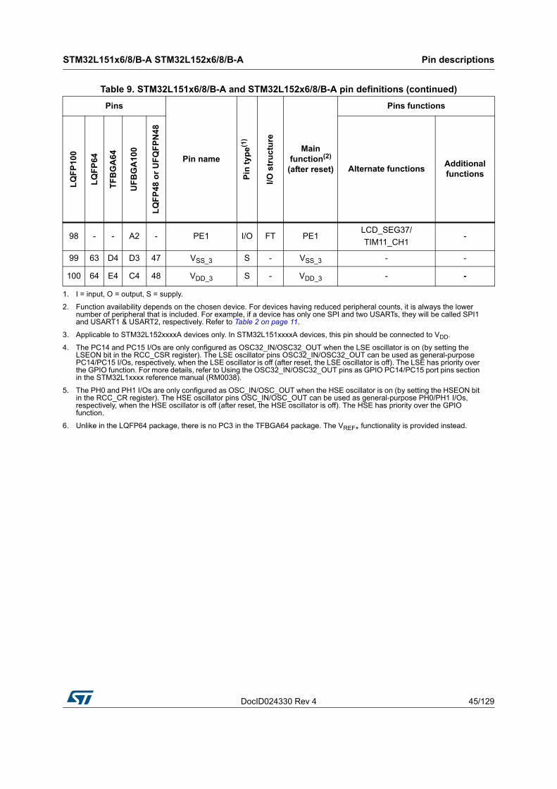
DocID024330 Rev 4 45/129
STM32L151x6/8/B-A STM32L152x6/8/B-A Pin descriptions
51
98 - - A2 - PE1 I/O FT PE1LCD_SEG37/
TIM11_CH1-
99 63 D4 D3 47 VSS_3 S - VSS_3 - -
100 64 E4 C4 48 VDD_3 S - VDD_3 - -
1. I = input, O = output, S = supply.
2. Function availability depends on the chosen device. For devices having reduced peripheral counts, it is always the lower number of peripheral that is included. For example, if a device has only one SPI and two USARTs, they will be called SPI1 and USART1 & USART2, respectively. Refer to Table 2 on page 11.
3. Applicable to STM32L152xxxxA devices only. In STM32L151xxxxA devices, this pin should be connected to VDD.
4. The PC14 and PC15 I/Os are only configured as OSC32_IN/OSC32_OUT when the LSE oscillator is on (by setting the LSEON bit in the RCC_CSR register). The LSE oscillator pins OSC32_IN/OSC32_OUT can be used as general-purpose PC14/PC15 I/Os, respectively, when the LSE oscillator is off (after reset, the LSE oscillator is off). The LSE has priority over the GPIO function. For more details, refer to Using the OSC32_IN/OSC32_OUT pins as GPIO PC14/PC15 port pins section in the STM32L1xxxx reference manual (RM0038).
5. The PH0 and PH1 I/Os are only configured as OSC_IN/OSC_OUT when the HSE oscillator is on (by setting the HSEON bit in the RCC_CR register). The HSE oscillator pins OSC_IN/OSC_OUT can be used as general-purpose PH0/PH1 I/Os, respectively, when the HSE oscillator is off (after reset, the HSE oscillator is off). The HSE has priority over the GPIO function.
6. Unlike in the LQFP64 package, there is no PC3 in the TFBGA64 package. The VREF+ functionality is provided instead.
Table 9. STM32L151x6/8/B-A and STM32L152x6/8/B-A pin definitions (continued)
Pins
Pin name
Pin
typ
e(1)
I/O s
tru
ctu
re
Main function(2)
(after reset)
Pins functions
LQ
FP
100
LQ
FP
64
TF
BG
A64
UF
BG
A1
00
LQ
FP
48 o
r U
FQ
FP
N48
Alternate functionsAdditional functions
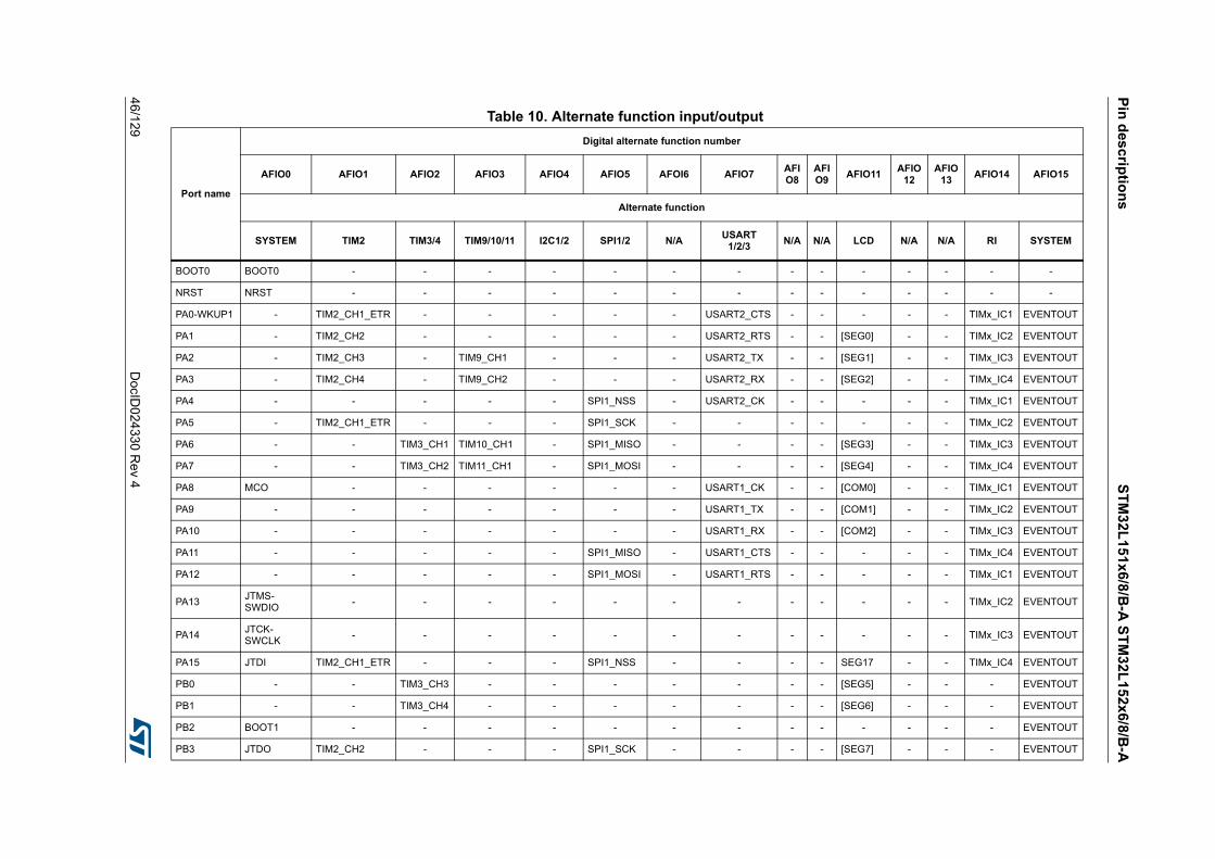
Pin
des
criptio
ns
ST
M3
2L1
51x
6/8/B
-A S
TM
32
L1
52x
6/8/B-A
46/1
29D
ocID024
330 Re
v 4
Table 10. Alternate function input/output
Port name
Digital alternate function number
AFIO0 AFIO1 AFIO2 AFIO3 AFIO4 AFIO5 AFOI6 AFIO7AFIO8
AFIO9
AFIO11AFIO
12AFIO
13AFIO14 AFIO15
Alternate function
SYSTEM TIM2 TIM3/4 TIM9/10/11 I2C1/2 SPI1/2 N/AUSART
1/2/3N/A N/A LCD N/A N/A RI SYSTEM
BOOT0 BOOT0 - - - - - - - - - - - - - -
NRST NRST - - - - - - - - - - - - - -
PA0-WKUP1 - TIM2_CH1_ETR - - - - - USART2_CTS - - - - - TIMx_IC1 EVENTOUT
PA1 - TIM2_CH2 - - - - - USART2_RTS - - [SEG0] - - TIMx_IC2 EVENTOUT
PA2 - TIM2_CH3 - TIM9_CH1 - - - USART2_TX - - [SEG1] - - TIMx_IC3 EVENTOUT
PA3 - TIM2_CH4 - TIM9_CH2 - - - USART2_RX - - [SEG2] - - TIMx_IC4 EVENTOUT
PA4 - - - - - SPI1_NSS - USART2_CK - - - - - TIMx_IC1 EVENTOUT
PA5 - TIM2_CH1_ETR - - - SPI1_SCK - - - - - - - TIMx_IC2 EVENTOUT
PA6 - - TIM3_CH1 TIM10_CH1 - SPI1_MISO - - - - [SEG3] - - TIMx_IC3 EVENTOUT
PA7 - - TIM3_CH2 TIM11_CH1 - SPI1_MOSI - - - - [SEG4] - - TIMx_IC4 EVENTOUT
PA8 MCO - - - - - - USART1_CK - - [COM0] - - TIMx_IC1 EVENTOUT
PA9 - - - - - - - USART1_TX - - [COM1] - - TIMx_IC2 EVENTOUT
PA10 - - - - - - - USART1_RX - - [COM2] - - TIMx_IC3 EVENTOUT
PA11 - - - - - SPI1_MISO - USART1_CTS - - - - - TIMx_IC4 EVENTOUT
PA12 - - - - - SPI1_MOSI - USART1_RTS - - - - - TIMx_IC1 EVENTOUT
PA13JTMS-SWDIO
- - - - - - - - - - - - TIMx_IC2 EVENTOUT
PA14JTCK-SWCLK
- - - - - - - - - - - - TIMx_IC3 EVENTOUT
PA15 JTDI TIM2_CH1_ETR - - - SPI1_NSS - - - - SEG17 - - TIMx_IC4 EVENTOUT
PB0 - - TIM3_CH3 - - - - - - - [SEG5] - - - EVENTOUT
PB1 - - TIM3_CH4 - - - - - - - [SEG6] - - - EVENTOUT
PB2 BOOT1 - - - - - - - - - - - - - EVENTOUT
PB3 JTDO TIM2_CH2 - - - SPI1_SCK - - - - [SEG7] - - - EVENTOUT
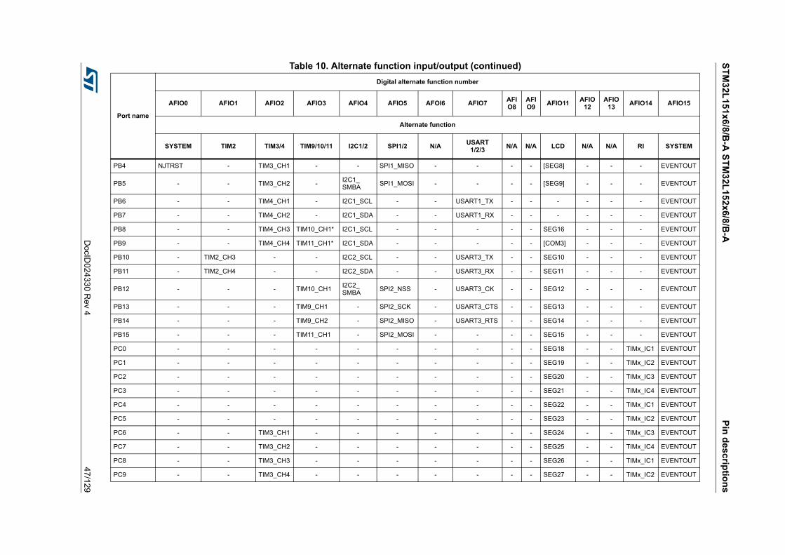
ST
M3
2L1
51x6
/8/B
-A S
TM
32L
15
2x6/8/B
-AP
in d
esc
riptio
ns
DocID
024330 R
ev 4
47/129
PB4 NJTRST - TIM3_CH1 - - SPI1_MISO - - - - [SEG8] - - - EVENTOUT
PB5 - - TIM3_CH2 -I2C1_ SMBA
SPI1_MOSI - - - - [SEG9] - - - EVENTOUT
PB6 - - TIM4_CH1 - I2C1_SCL - - USART1_TX - - - - - - EVENTOUT
PB7 - - TIM4_CH2 - I2C1_SDA - - USART1_RX - - - - - - EVENTOUT
PB8 - - TIM4_CH3 TIM10_CH1* I2C1_SCL - - - - - SEG16 - - - EVENTOUT
PB9 - - TIM4_CH4 TIM11_CH1* I2C1_SDA - - - - - [COM3] - - - EVENTOUT
PB10 - TIM2_CH3 - - I2C2_SCL - - USART3_TX - - SEG10 - - - EVENTOUT
PB11 - TIM2_CH4 - - I2C2_SDA - - USART3_RX - - SEG11 - - - EVENTOUT
PB12 - - - TIM10_CH1 I2C2_ SMBA
SPI2_NSS - USART3_CK - - SEG12 - - - EVENTOUT
PB13 - - - TIM9_CH1 - SPI2_SCK - USART3_CTS - - SEG13 - - - EVENTOUT
PB14 - - - TIM9_CH2 - SPI2_MISO - USART3_RTS - - SEG14 - - - EVENTOUT
PB15 - - - TIM11_CH1 - SPI2_MOSI - - - - SEG15 - - - EVENTOUT
PC0 - - - - - - - - - - SEG18 - - TIMx_IC1 EVENTOUT
PC1 - - - - - - - - - - SEG19 - - TIMx_IC2 EVENTOUT
PC2 - - - - - - - - - - SEG20 - - TIMx_IC3 EVENTOUT
PC3 - - - - - - - - - - SEG21 - - TIMx_IC4 EVENTOUT
PC4 - - - - - - - - - - SEG22 - - TIMx_IC1 EVENTOUT
PC5 - - - - - - - - - - SEG23 - - TIMx_IC2 EVENTOUT
PC6 - - TIM3_CH1 - - - - - - - SEG24 - - TIMx_IC3 EVENTOUT
PC7 - - TIM3_CH2 - - - - - - - SEG25 - - TIMx_IC4 EVENTOUT
PC8 - - TIM3_CH3 - - - - - - - SEG26 - - TIMx_IC1 EVENTOUT
PC9 - - TIM3_CH4 - - - - - - - SEG27 - - TIMx_IC2 EVENTOUT
Table 10. Alternate function input/output (continued)
Port name
Digital alternate function number
AFIO0 AFIO1 AFIO2 AFIO3 AFIO4 AFIO5 AFOI6 AFIO7AFIO8
AFIO9
AFIO11AFIO
12AFIO
13AFIO14 AFIO15
Alternate function
SYSTEM TIM2 TIM3/4 TIM9/10/11 I2C1/2 SPI1/2 N/AUSART
1/2/3N/A N/A LCD N/A N/A RI SYSTEM
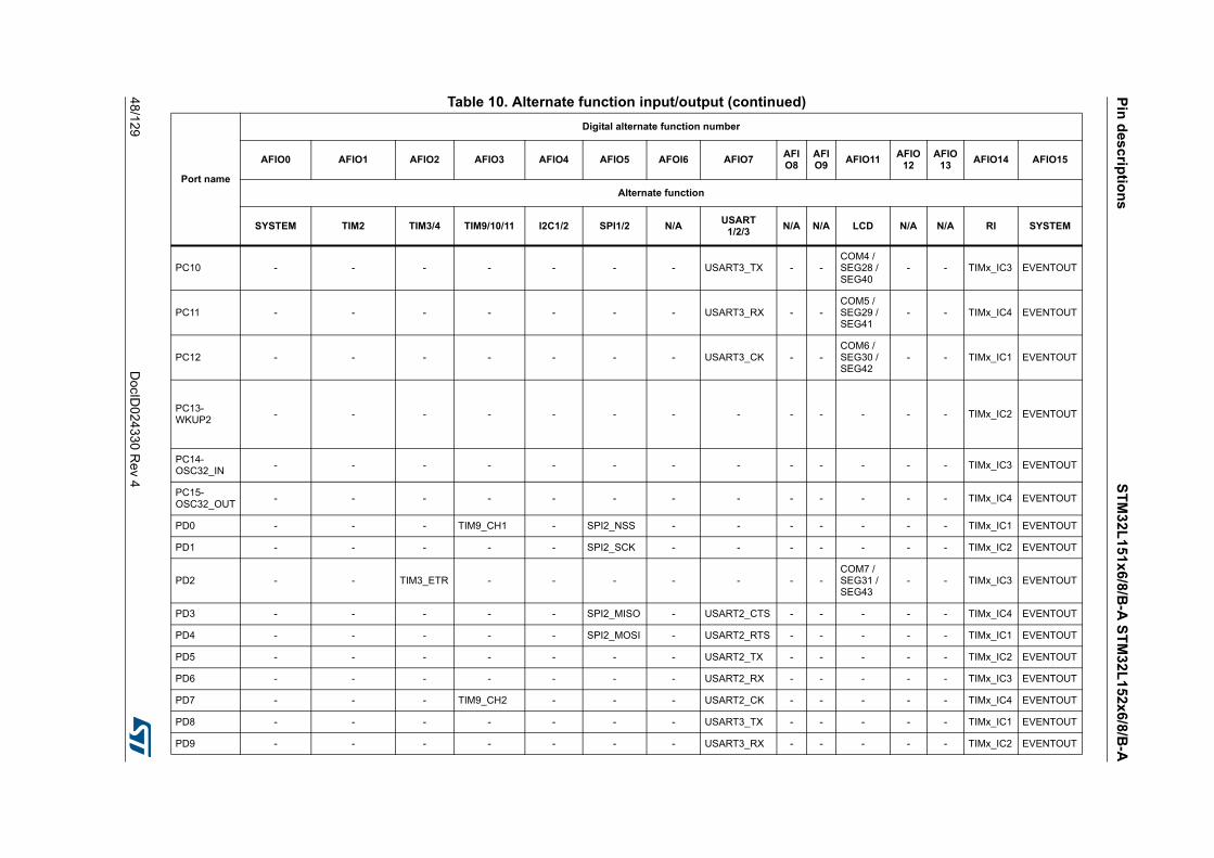
Pin
des
criptio
ns
ST
M3
2L1
51x
6/8/B
-A S
TM
32
L1
52x
6/8/B-A
48/1
29D
ocID024
330 Re
v 4
PC10 - - - - - - - USART3_TX - -COM4 / SEG28 / SEG40
- - TIMx_IC3 EVENTOUT
PC11 - - - - - - - USART3_RX - -COM5 / SEG29 / SEG41
- - TIMx_IC4 EVENTOUT
PC12 - - - - - - - USART3_CK - -COM6 / SEG30 / SEG42
- - TIMx_IC1 EVENTOUT
PC13-WKUP2
- - - - - - - - - - - - - TIMx_IC2 EVENTOUT
PC14-OSC32_IN
- - - - - - - - - - - - - TIMx_IC3 EVENTOUT
PC15-OSC32_OUT
- - - - - - - - - - - - - TIMx_IC4 EVENTOUT
PD0 - - - TIM9_CH1 - SPI2_NSS - - - - - - - TIMx_IC1 EVENTOUT
PD1 - - - - - SPI2_SCK - - - - - - - TIMx_IC2 EVENTOUT
PD2 - - TIM3_ETR - - - - - - -COM7 / SEG31 / SEG43
- - TIMx_IC3 EVENTOUT
PD3 - - - - - SPI2_MISO - USART2_CTS - - - - - TIMx_IC4 EVENTOUT
PD4 - - - - - SPI2_MOSI - USART2_RTS - - - - - TIMx_IC1 EVENTOUT
PD5 - - - - - - - USART2_TX - - - - - TIMx_IC2 EVENTOUT
PD6 - - - - - - - USART2_RX - - - - - TIMx_IC3 EVENTOUT
PD7 - - - TIM9_CH2 - - - USART2_CK - - - - - TIMx_IC4 EVENTOUT
PD8 - - - - - - - USART3_TX - - - - - TIMx_IC1 EVENTOUT
PD9 - - - - - - - USART3_RX - - - - - TIMx_IC2 EVENTOUT
Table 10. Alternate function input/output (continued)
Port name
Digital alternate function number
AFIO0 AFIO1 AFIO2 AFIO3 AFIO4 AFIO5 AFOI6 AFIO7AFIO8
AFIO9
AFIO11AFIO
12AFIO
13AFIO14 AFIO15
Alternate function
SYSTEM TIM2 TIM3/4 TIM9/10/11 I2C1/2 SPI1/2 N/AUSART
1/2/3N/A N/A LCD N/A N/A RI SYSTEM
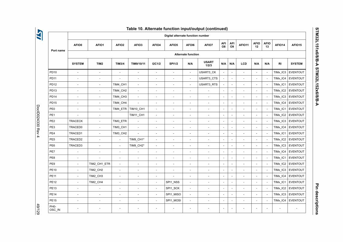
ST
M3
2L1
51x6
/8/B
-A S
TM
32L
15
2x6/8/B
-AP
in d
esc
riptio
ns
DocID
024330 R
ev 4
49/129
PD10 - - - - - - - USART3_CK - - - - - TIMx_IC3 EVENTOUT
PD11 - - - - - - - USART3_CTS - - - - - TIMx_IC4 EVENTOUT
PD12 - - TIM4_CH1 - - - - USART3_RTS - - - - - TIMx_IC1 EVENTOUT
PD13 - - TIM4_CH2 - - - - - - - - - - TIMx_IC2 EVENTOUT
PD14 - - TIM4_CH3 - - - - - - - - - - TIMx_IC3 EVENTOUT
PD15 - - TIM4_CH4 - - - - - - - - - - TIMx_IC4 EVENTOUT
PE0 - - TIM4_ETR TIM10_CH1 - - - - - - - - - TIMx_IC1 EVENTOUT
PE1 - - TIM11_CH1 - - - - - - - - - TIMx_IC2 EVENTOUT
PE2 TRACECK - TIM3_ETR - - - - - - - - - - TIMx_IC3 EVENTOUT
PE3 TRACED0 - TIM3_CH1 - - - - - - - - - - TIMx_IC4 EVENTOUT
PE4 TRACED1 - TIM3_CH2 - - - - - - - - - - TIMx_IC1 EVENTOUT
PE5 TRACED2 - - TIM9_CH1* - - - - - - - - - TIMx_IC2 EVENTOUT
PE6 TRACED3 - - TIM9_CH2* - - - - - - - - - TIMx_IC3 EVENTOUT
PE7 - - - - - - - - - - - - - TIMx_IC4 EVENTOUT
PE8 - - - - - - - - - - - - - TIMx_IC1 EVENTOUT
PE9 - TIM2_CH1_ETR - - - - - - - - - - - TIMx_IC2 EVENTOUT
PE10 - TIM2_CH2 - - - - - - - - - - - TIMx_IC3 EVENTOUT
PE11 - TIM2_CH3 - - - - - - - - - - - TIMx_IC4 EVENTOUT
PE12 - TIM2_CH4 - - - SPI1_NSS - - - - - - - TIMx_IC1 EVENTOUT
PE13 - - - - - SPI1_SCK - - - - - - - TIMx_IC2 EVENTOUT
PE14 - - - - - SPI1_MISO - - - - - - - TIMx_IC3 EVENTOUT
PE15 - - - - - SPI1_MOSI - - - - - - - TIMx_IC4 EVENTOUT
PH0-OSC_IN
- - - - - - - - - - - - - - -
Table 10. Alternate function input/output (continued)
Port name
Digital alternate function number
AFIO0 AFIO1 AFIO2 AFIO3 AFIO4 AFIO5 AFOI6 AFIO7AFIO8
AFIO9
AFIO11AFIO
12AFIO
13AFIO14 AFIO15
Alternate function
SYSTEM TIM2 TIM3/4 TIM9/10/11 I2C1/2 SPI1/2 N/AUSART
1/2/3N/A N/A LCD N/A N/A RI SYSTEM
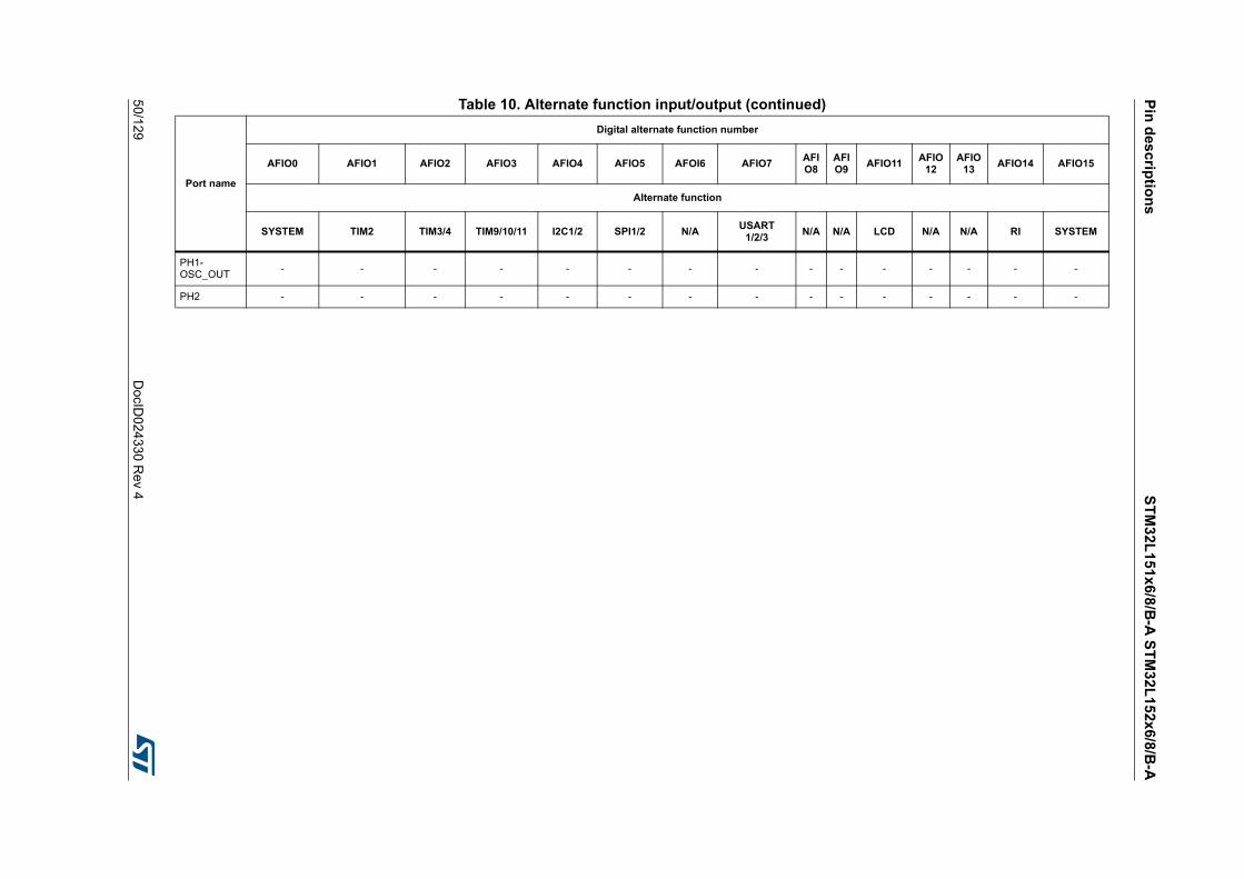
Pin
des
criptio
ns
ST
M3
2L1
51x
6/8/B
-A S
TM
32
L1
52x
6/8/B-A
50/1
29D
ocID024
330 Re
v 4
PH1-OSC_OUT
- - - - - - - - - - - - - - -
PH2 - - - - - - - - - - - - - - -
Table 10. Alternate function input/output (continued)
Port name
Digital alternate function number
AFIO0 AFIO1 AFIO2 AFIO3 AFIO4 AFIO5 AFOI6 AFIO7AFIO8
AFIO9
AFIO11AFIO
12AFIO
13AFIO14 AFIO15
Alternate function
SYSTEM TIM2 TIM3/4 TIM9/10/11 I2C1/2 SPI1/2 N/AUSART
1/2/3N/A N/A LCD N/A N/A RI SYSTEM
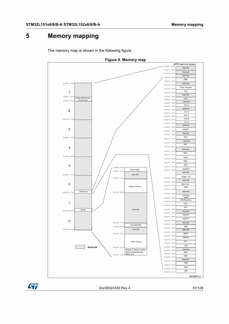
DocID024330 Rev 4 51/129
STM32L151x6/8/B-A STM32L152x6/8/B-A Memory mapping
51
5 Memory mapping
The memory map is shown in the following figure.
Figure 9. Memory map
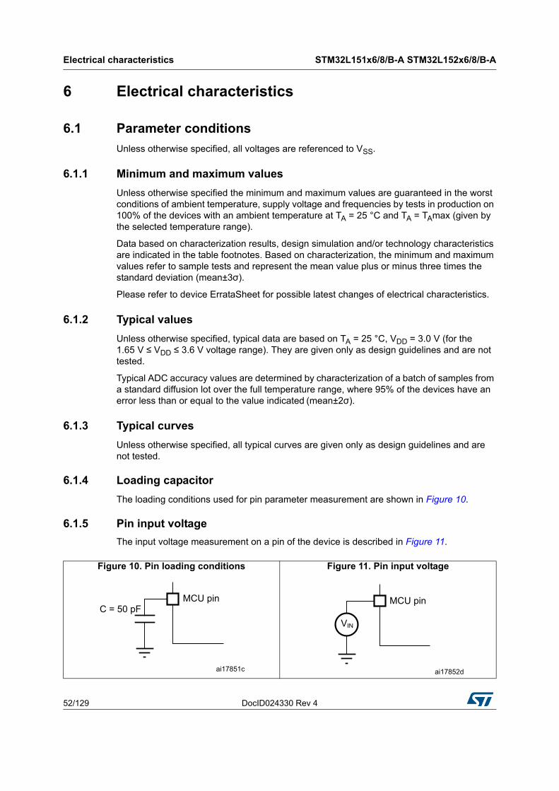
Electrical characteristics STM32L151x6/8/B-A STM32L152x6/8/B-A
52/129 DocID024330 Rev 4
6 Electrical characteristics
6.1 Parameter conditions
Unless otherwise specified, all voltages are referenced to VSS.
6.1.1 Minimum and maximum values
Unless otherwise specified the minimum and maximum values are guaranteed in the worst conditions of ambient temperature, supply voltage and frequencies by tests in production on 100% of the devices with an ambient temperature at TA = 25 °C and TA = TAmax (given by the selected temperature range).
Data based on characterization results, design simulation and/or technology characteristics are indicated in the table footnotes. Based on characterization, the minimum and maximum values refer to sample tests and represent the mean value plus or minus three times the standard deviation (mean±3σ).
Please refer to device ErrataSheet for possible latest changes of electrical characteristics.
6.1.2 Typical values
Unless otherwise specified, typical data are based on TA = 25 °C, VDD = 3.0 V (for the 1.65 V ≤ VDD ≤ 3.6 V voltage range). They are given only as design guidelines and are not tested.
Typical ADC accuracy values are determined by characterization of a batch of samples from a standard diffusion lot over the full temperature range, where 95% of the devices have an error less than or equal to the value indicated (mean±2σ).
6.1.3 Typical curves
Unless otherwise specified, all typical curves are given only as design guidelines and are not tested.
6.1.4 Loading capacitor
The loading conditions used for pin parameter measurement are shown in Figure 10.
6.1.5 Pin input voltage
The input voltage measurement on a pin of the device is described in Figure 11.
Figure 10. Pin loading conditions Figure 11. Pin input voltage
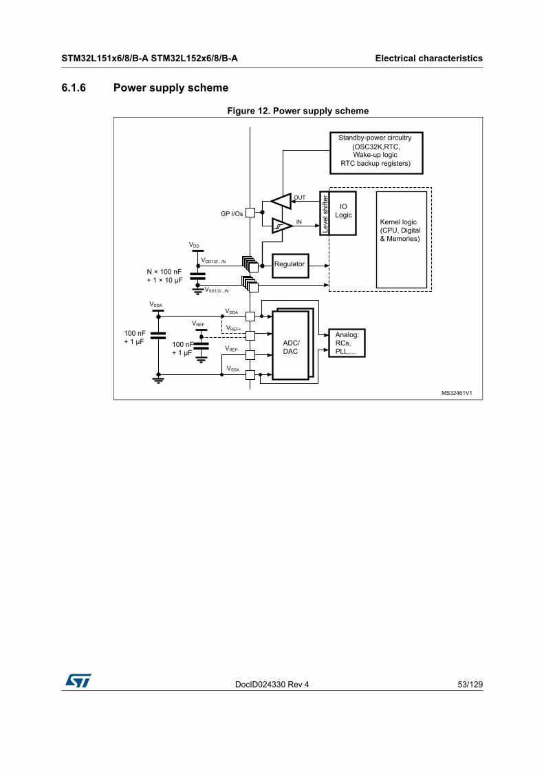
DocID024330 Rev 4 53/129
STM32L151x6/8/B-A STM32L152x6/8/B-A Electrical characteristics
105
6.1.6 Power supply scheme
Figure 12. Power supply scheme
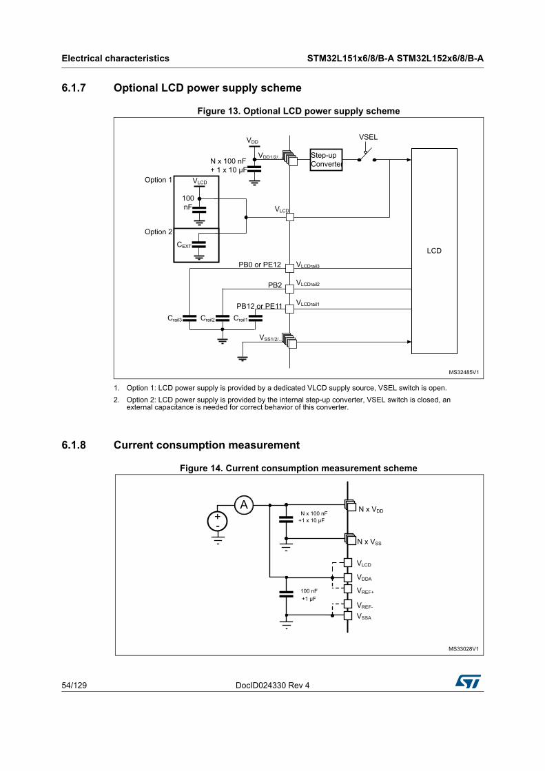
Electrical characteristics STM32L151x6/8/B-A STM32L152x6/8/B-A
54/129 DocID024330 Rev 4
6.1.7 Optional LCD power supply scheme
Figure 13. Optional LCD power supply scheme
1. Option 1: LCD power supply is provided by a dedicated VLCD supply source, VSEL switch is open.
2. Option 2: LCD power supply is provided by the internal step-up converter, VSEL switch is closed, an external capacitance is needed for correct behavior of this converter.
6.1.8 Current consumption measurement
Figure 14. Current consumption measurement scheme
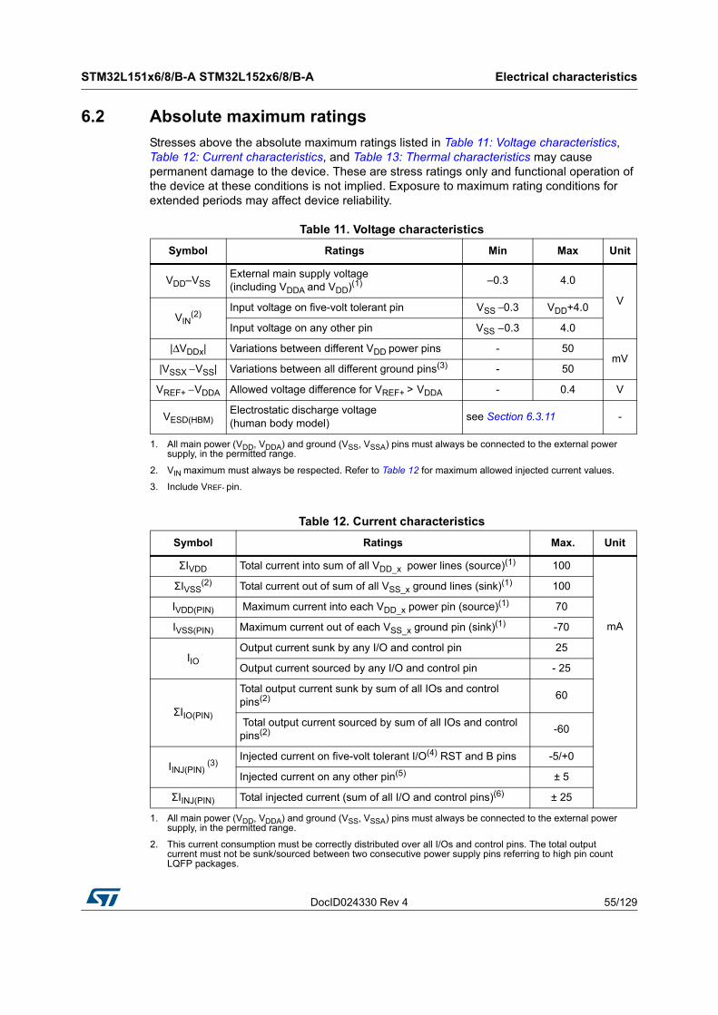
DocID024330 Rev 4 55/129
STM32L151x6/8/B-A STM32L152x6/8/B-A Electrical characteristics
105
6.2 Absolute maximum ratings
Stresses above the absolute maximum ratings listed in Table 11: Voltage characteristics, Table 12: Current characteristics, and Table 13: Thermal characteristics may cause permanent damage to the device. These are stress ratings only and functional operation of the device at these conditions is not implied. Exposure to maximum rating conditions for extended periods may affect device reliability.
Table 11. Voltage characteristics
Symbol Ratings Min Max Unit
VDD–VSSExternal main supply voltage (including VDDA and VDD)(1)
1. All main power (VDD, VDDA) and ground (VSS, VSSA) pins must always be connected to the external power supply, in the permitted range.
–0.3 4.0
V
VIN(2)
2. VIN maximum must always be respected. Refer to Table 12 for maximum allowed injected current values.
Input voltage on five-volt tolerant pin VSS − 0.3 VDD+4.0
Input voltage on any other pin VSS − 0.3 4.0
|ΔVDDx| Variations between different VDD power pins - 50mV
|VSSX − VSS| Variations between all different ground pins(3)
3. Include VREF- pin.
- 50
VREF+ − VDDA Allowed voltage difference for VREF+ > VDDA - 0.4 V
VESD(HBM)Electrostatic discharge voltage (human body model)
see Section 6.3.11 -
Table 12. Current characteristics
Symbol Ratings Max. Unit
ΣIVDD Total current into sum of all VDD_x power lines (source)(1)
1. All main power (VDD, VDDA) and ground (VSS, VSSA) pins must always be connected to the external power supply, in the permitted range.
100
mA
ΣIVSS(2)
2. This current consumption must be correctly distributed over all I/Os and control pins. The total output current must not be sunk/sourced between two consecutive power supply pins referring to high pin count LQFP packages.
Total current out of sum of all VSS_x ground lines (sink)(1) 100
IVDD(PIN) Maximum current into each VDD_x power pin (source)(1) 70
IVSS(PIN) Maximum current out of each VSS_x ground pin (sink)(1) -70
IIOOutput current sunk by any I/O and control pin 25
Output current sourced by any I/O and control pin - 25
ΣIIO(PIN)
Total output current sunk by sum of all IOs and control pins(2) 60
Total output current sourced by sum of all IOs and control pins(2) -60
IINJ(PIN) (3)
Injected current on five-volt tolerant I/O(4) RST and B pins -5/+0
Injected current on any other pin(5) ± 5
ΣIINJ(PIN) Total injected current (sum of all I/O and control pins)(6) ± 25
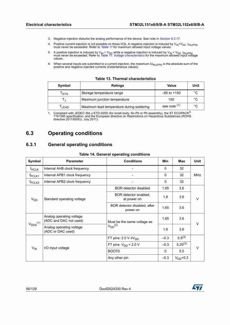
Electrical characteristics STM32L151x6/8/B-A STM32L152x6/8/B-A
56/129 DocID024330 Rev 4
6.3 Operating conditions
6.3.1 General operating conditions
3. Negative injection disturbs the analog performance of the device. See note in Section 6.3.17.
4. Positive current injection is not possible on these I/Os. A negative injection is induced by VIN<VSS. IINJ(PIN) must never be exceeded. Refer to Table 11 for maximum allowed input voltage values.
5. A positive injection is induced by VIN > VDD while a negative injection is induced by VIN < VSS. IINJ(PIN) must never be exceeded. Refer to Table 11: Voltage characteristics for the maximum allowed input voltage values.
6. When several inputs are submitted to a current injection, the maximum ΣIINJ(PIN) is the absolute sum of the positive and negative injected currents (instantaneous values).
Table 13. Thermal characteristics
Symbol Ratings Value Unit
TSTG Storage temperature range –65 to +150 °C
TJ Maximum junction temperature 150 °C
TLEAD Maximum lead temperature during soldering see note (1)
1. Compliant with JEDEC Std J-STD-020D (for small body, Sn-Pb or Pb assembly), the ST ECOPACK® 7191395 specification, and the European directive on Restrictions on Hazardous Substances (ROHS directive 2011/65/EU, July 2011).
°C
Table 14. General operating conditions
Symbol Parameter Conditions Min Max Unit
fHCLK Internal AHB clock frequency - 0 32
MHzfPCLK1 Internal APB1 clock frequency - 0 32
fPCLK2 Internal APB2 clock frequency - 0 32
VDD Standard operating voltage
BOR detector disabled 1.65 3.6
VBOR detector enabled,
at power on1.8 3.6
BOR detector disabled, after power on
1.65 3.6
VDDA(1)
Analog operating voltage (ADC and DAC not used) Must be the same voltage as
VDD(2)
1.65 3.6
VAnalog operating voltage (ADC or DAC used)
1.8 3.6
VIN I/O input voltage
FT pins: 2.0 V ≤VDD –0.3 5.5(3)
VFT pins: VDD < 2.0 V –0.3 5.25(3)
BOOT0 0 5.5
Any other pin –0.3 VDD+0.3
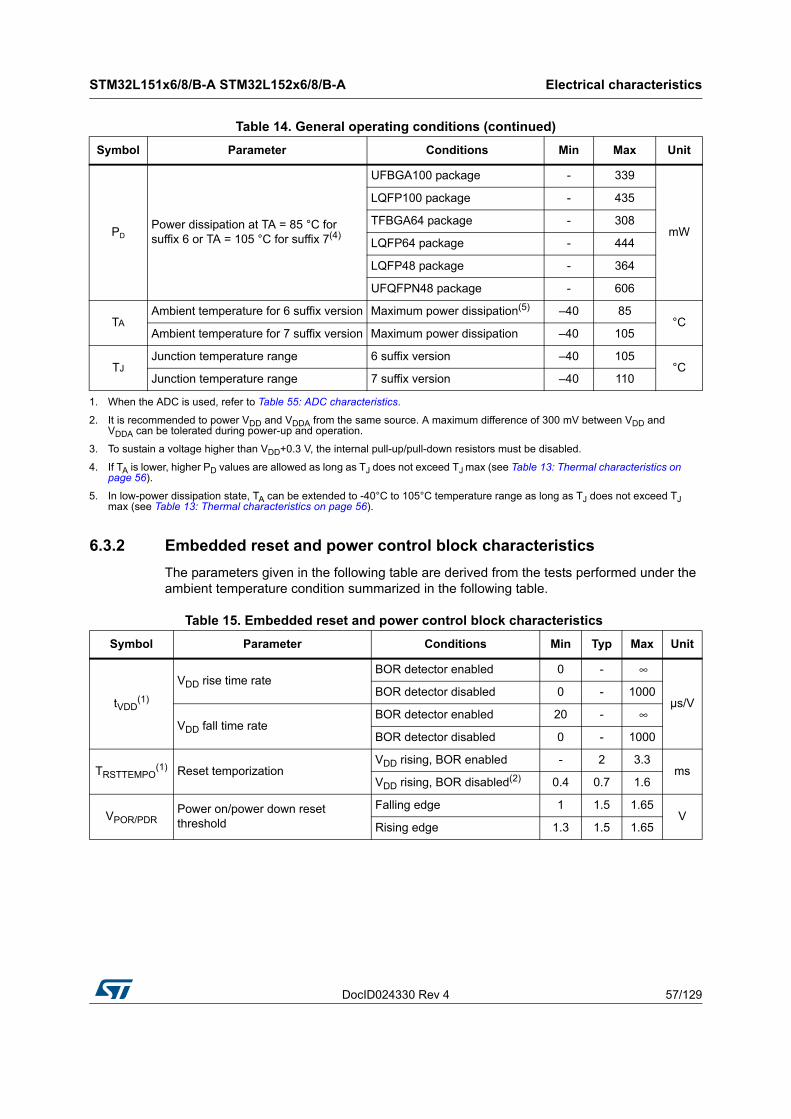
DocID024330 Rev 4 57/129
STM32L151x6/8/B-A STM32L152x6/8/B-A Electrical characteristics
105
6.3.2 Embedded reset and power control block characteristics
The parameters given in the following table are derived from the tests performed under the ambient temperature condition summarized in the following table.
PDPower dissipation at TA = 85 °C for suffix 6 or TA = 105 °C for suffix 7(4)
UFBGA100 package - 339
mW
LQFP100 package - 435
TFBGA64 package - 308
LQFP64 package - 444
LQFP48 package - 364
UFQFPN48 package - 606
TA Ambient temperature for 6 suffix version Maximum power dissipation(5) –40 85
°CAmbient temperature for 7 suffix version Maximum power dissipation –40 105
TJ Junction temperature range 6 suffix version –40 105
°CJunction temperature range 7 suffix version –40 110
1. When the ADC is used, refer to Table 55: ADC characteristics.
2. It is recommended to power VDD and VDDA from the same source. A maximum difference of 300 mV between VDD and VDDA can be tolerated during power-up and operation.
3. To sustain a voltage higher than VDD+0.3 V, the internal pull-up/pull-down resistors must be disabled.
4. If TA is lower, higher PD values are allowed as long as TJ does not exceed TJ max (see Table 13: Thermal characteristics on page 56).
5. In low-power dissipation state, TA can be extended to -40°C to 105°C temperature range as long as TJ does not exceed TJ max (see Table 13: Thermal characteristics on page 56).
Table 14. General operating conditions (continued)
Symbol Parameter Conditions Min Max Unit
Table 15. Embedded reset and power control block characteristics
Symbol Parameter Conditions Min Typ Max Unit
tVDD(1)
VDD rise time rateBOR detector enabled 0 - ∞
µs/VBOR detector disabled 0 - 1000
VDD fall time rateBOR detector enabled 20 - ∞
BOR detector disabled 0 - 1000
TRSTTEMPO(1) Reset temporization
VDD rising, BOR enabled - 2 3.3ms
VDD rising, BOR disabled(2) 0.4 0.7 1.6
VPOR/PDRPower on/power down reset threshold
Falling edge 1 1.5 1.65V
Rising edge 1.3 1.5 1.65
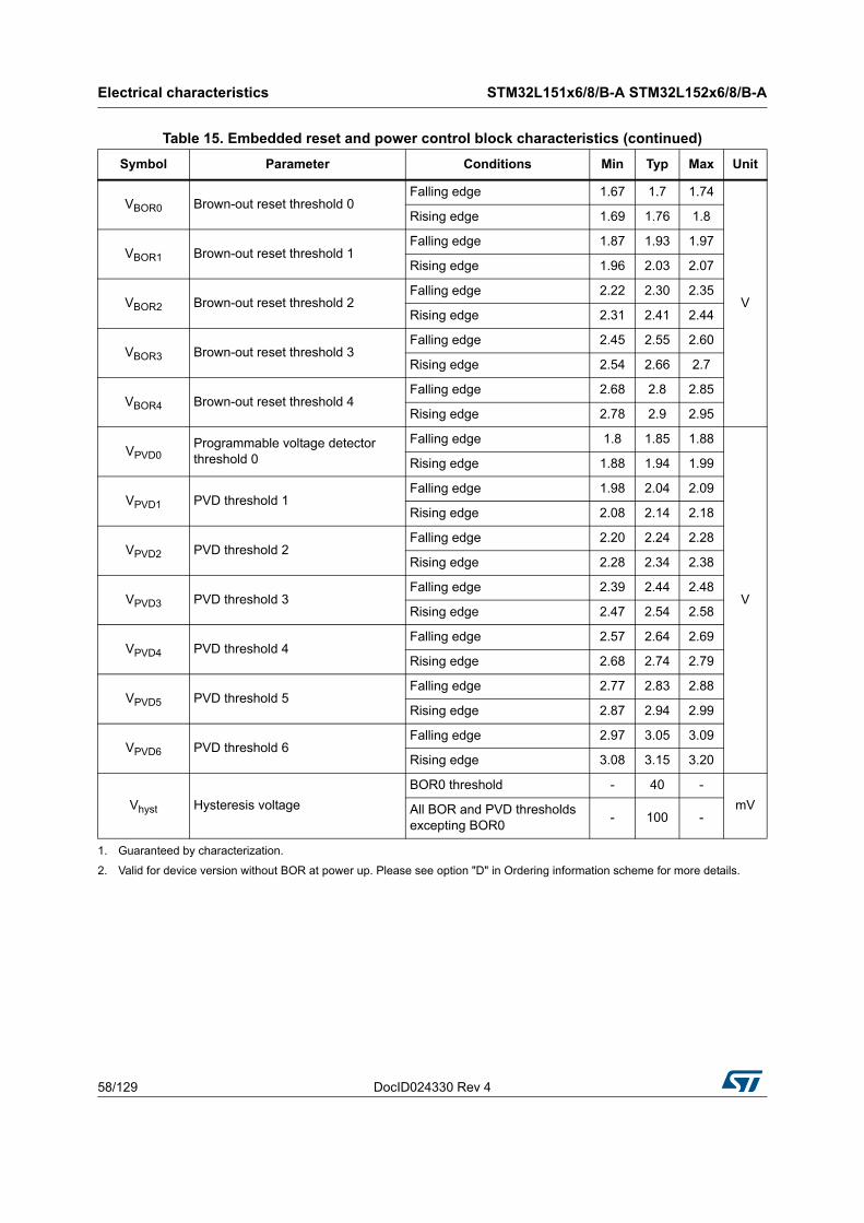
Electrical characteristics STM32L151x6/8/B-A STM32L152x6/8/B-A
58/129 DocID024330 Rev 4
VBOR0 Brown-out reset threshold 0Falling edge 1.67 1.7 1.74
V
Rising edge 1.69 1.76 1.8
VBOR1 Brown-out reset threshold 1Falling edge 1.87 1.93 1.97
Rising edge 1.96 2.03 2.07
VBOR2 Brown-out reset threshold 2Falling edge 2.22 2.30 2.35
Rising edge 2.31 2.41 2.44
VBOR3 Brown-out reset threshold 3Falling edge 2.45 2.55 2.60
Rising edge 2.54 2.66 2.7
VBOR4 Brown-out reset threshold 4Falling edge 2.68 2.8 2.85
Rising edge 2.78 2.9 2.95
VPVD0Programmable voltage detector threshold 0
Falling edge 1.8 1.85 1.88
V
Rising edge 1.88 1.94 1.99
VPVD1 PVD threshold 1Falling edge 1.98 2.04 2.09
Rising edge 2.08 2.14 2.18
VPVD2 PVD threshold 2Falling edge 2.20 2.24 2.28
Rising edge 2.28 2.34 2.38
VPVD3 PVD threshold 3Falling edge 2.39 2.44 2.48
Rising edge 2.47 2.54 2.58
VPVD4 PVD threshold 4Falling edge 2.57 2.64 2.69
Rising edge 2.68 2.74 2.79
VPVD5 PVD threshold 5Falling edge 2.77 2.83 2.88
Rising edge 2.87 2.94 2.99
VPVD6 PVD threshold 6Falling edge 2.97 3.05 3.09
Rising edge 3.08 3.15 3.20
Vhyst Hysteresis voltage
BOR0 threshold - 40 -
mVAll BOR and PVD thresholds excepting BOR0
- 100 -
1. Guaranteed by characterization.
2. Valid for device version without BOR at power up. Please see option "D" in Ordering information scheme for more details.
Table 15. Embedded reset and power control block characteristics (continued)
Symbol Parameter Conditions Min Typ Max Unit
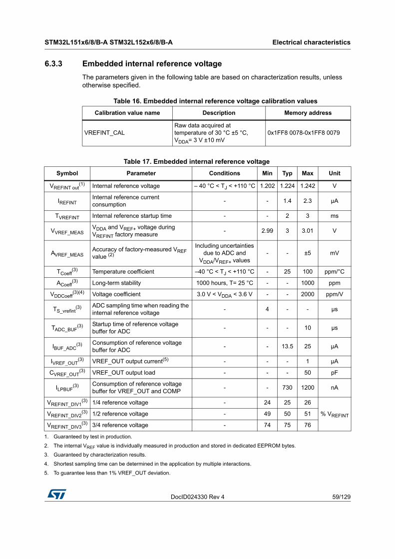
DocID024330 Rev 4 59/129
STM32L151x6/8/B-A STM32L152x6/8/B-A Electrical characteristics
105
6.3.3 Embedded internal reference voltage
The parameters given in the following table are based on characterization results, unless otherwise specified.
Table 16. Embedded internal reference voltage calibration values
Calibration value name Description Memory address
VREFINT_CALRaw data acquired at temperature of 30 °C ±5 °C, VDDA= 3 V ±10 mV
0x1FF8 0078-0x1FF8 0079
Table 17. Embedded internal reference voltage
Symbol Parameter Conditions Min Typ Max Unit
VREFINT out(1) Internal reference voltage – 40 °C < TJ < +110 °C 1.202 1.224 1.242 V
IREFINTInternal reference current consumption
- - 1.4 2.3 µA
TVREFINT Internal reference startup time - - 2 3 ms
VVREF_MEASVDDA and VREF+ voltage during VREFINT factory measure
- 2.99 3 3.01 V
AVREF_MEASAccuracy of factory-measured VREF value (2)
Including uncertainties due to ADC and
VDDA/VREF+ values- - ±5 mV
TCoeff(3) Temperature coefficient –40 °C < TJ < +110 °C - 25 100 ppm/°C
ACoeff(3) Long-term stability 1000 hours, T= 25 °C - - 1000 ppm
VDDCoeff(3)(4) Voltage coefficient 3.0 V < VDDA < 3.6 V - - 2000 ppm/V
TS_vrefint(3) ADC sampling time when reading the
internal reference voltage- 4 - - µs
TADC_BUF(3) Startup time of reference voltage
buffer for ADC- - - 10 µs
IBUF_ADC(3) Consumption of reference voltage
buffer for ADC- - 13.5 25 µA
IVREF_OUT(3) VREF_OUT output current(5) - - - 1 µA
CVREF_OUT(3) VREF_OUT output load - - - 50 pF
ILPBUF(3) Consumption of reference voltage
buffer for VREF_OUT and COMP - - 730 1200 nA
VREFINT_DIV1(3) 1/4 reference voltage - 24 25 26
% VREFINTVREFINT_DIV2(3) 1/2 reference voltage - 49 50 51
VREFINT_DIV3(3) 3/4 reference voltage - 74 75 76
1. Guaranteed by test in production.
2. The internal VREF value is individually measured in production and stored in dedicated EEPROM bytes.
3. Guaranteed by characterization results.
4. Shortest sampling time can be determined in the application by multiple interactions.
5. To guarantee less than 1% VREF_OUT deviation.
Electrical characteristics STM32L151x6/8/B-A STM32L152x6/8/B-A
60/129 DocID024330 Rev 4
6.3.4 Supply current characteristics
The current consumption is a function of several parameters and factors such as the operating voltage, ambient temperature, I/O pin loading, device software configuration, operating frequencies, I/O pin switching rate, program location in memory and executed binary code. The current consumption is measured as described in Figure 14: Current consumption measurement scheme.
All Run-mode current consumption measurements given in this section are performed with a reduced code that gives a consumption equivalent to Dhrystone 2.1 code, unless otherwise specified.
The current consumption values are derived from the tests performed under ambient temperature TA=25°C and VDD supply voltage conditions summarized in Table 14: General operating conditions, unless otherwise specified.
The MCU is placed under the following conditions:
• All I/O pins are configured in analog input mode.
• All peripherals are disabled except when explicitly mentioned.
• The Flash memory access time, 64-bit access and prefetch is adjusted depending on fHCLK frequency and voltage range to provide the best CPU performance.
• When the peripherals are enabled fAPB1 = fAPB2 = fAHB.
• When PLL is ON, the PLL inputs are equal to HSI = 16 MHz (if internal clock is used) or HSE = 16 MHz (if HSE bypass mode is used).
• The HSE user clock applied to OSC_IN input follows the characteristics specified in Table 27: High-speed external user clock characteristics.
• For maximum current consumption VDD = VDDA = 3.6 V is applied to all supply pins.
• For typical current consumption VDD = VDDA = 3.0 V is applied to all supply pins if not specified otherwise.
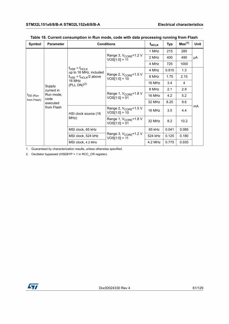
DocID024330 Rev 4 61/129
STM32L151x6/8/B-A STM32L152x6/8/B-A Electrical characteristics
105
Table 18. Current consumption in Run mode, code with data processing running from Flash
Symbol Parameter Conditions fHCLK Typ Max(1) Unit
IDD (Run
from Flash)
Supply current in Run mode, code executed from Flash
fHSE = fHCLK up to 16 MHz, included fHSE = fHCLK/2 above 16 MHz (PLL ON)(2)
Range 3, VCORE=1.2 V VOS[1:0] = 11
1 MHz 215 285
µA2 MHz 400 490
4 MHz 725 1000
Range 2, VCORE=1.5 V VOS[1:0] = 10
4 MHz 0.915 1.3
mA
8 MHz 1.75 2.15
16 MHz 3.4 4
Range 1, VCORE=1.8 V VOS[1:0] = 01
8 MHz 2.1 2.9
16 MHz 4.2 5.2
32 MHz 8.25 9.6
HSI clock source (16 MHz)
Range 2, VCORE=1.5 V VOS[1:0] = 10
16 MHz 3.5 4.4
Range 1, VCORE=1.8 V VOS[1:0] = 01
32 MHz 8.2 10.2
MSI clock, 65 kHzRange 3, VCORE=1.2 V VOS[1:0] = 11
65 kHz 0.041 0.085
MSI clock, 524 kHz 524 kHz 0.125 0.180
MSI clock, 4.2 MHz 4.2 MHz 0.775 0.935
1. Guaranteed by characterization results, unless otherwise specified.
2. Oscillator bypassed (HSEBYP = 1 in RCC_CR register).
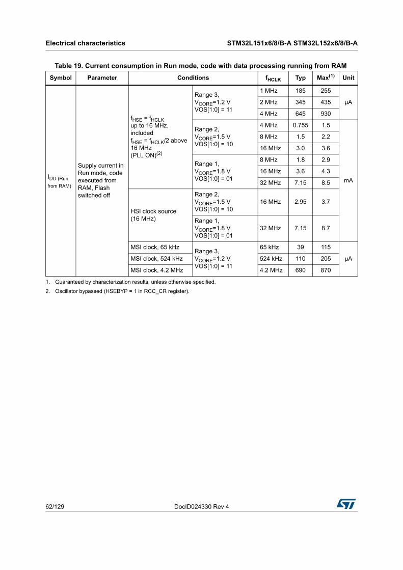
Electrical characteristics STM32L151x6/8/B-A STM32L152x6/8/B-A
62/129 DocID024330 Rev 4
Table 19. Current consumption in Run mode, code with data processing running from RAM
Symbol Parameter Conditions fHCLK Typ Max(1) Unit
IDD (Run
from RAM)
Supply current in Run mode, code executed from RAM, Flash switched off
fHSE = fHCLK up to 16 MHz, included fHSE = fHCLK/2 above 16 MHz (PLL ON)(2)
Range 3, VCORE=1.2 V VOS[1:0] = 11
1 MHz 185 255
µA2 MHz 345 435
4 MHz 645 930
Range 2, VCORE=1.5 V VOS[1:0] = 10
4 MHz 0.755 1.5
mA
8 MHz 1.5 2.2
16 MHz 3.0 3.6
Range 1, VCORE=1.8 V VOS[1:0] = 01
8 MHz 1.8 2.9
16 MHz 3.6 4.3
32 MHz 7.15 8.5
HSI clock source (16 MHz)
Range 2, VCORE=1.5 V VOS[1:0] = 10
16 MHz 2.95 3.7
Range 1, VCORE=1.8 V VOS[1:0] = 01
32 MHz 7.15 8.7
MSI clock, 65 kHzRange 3, VCORE=1.2 V VOS[1:0] = 11
65 kHz 39 115
µAMSI clock, 524 kHz 524 kHz 110 205
MSI clock, 4.2 MHz 4.2 MHz 690 870
1. Guaranteed by characterization results, unless otherwise specified.
2. Oscillator bypassed (HSEBYP = 1 in RCC_CR register).
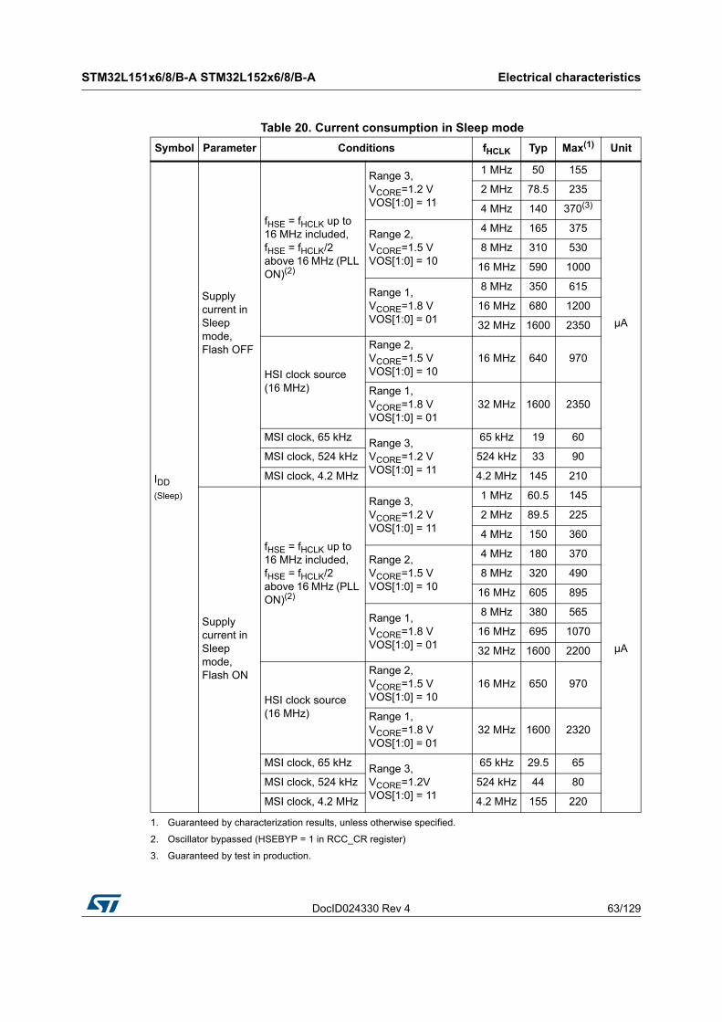
DocID024330 Rev 4 63/129
STM32L151x6/8/B-A STM32L152x6/8/B-A Electrical characteristics
105
Table 20. Current consumption in Sleep mode
Symbol Parameter Conditions fHCLK Typ Max(1)
1. Guaranteed by characterization results, unless otherwise specified.
Unit
IDD
(Sleep)
Supply current in Sleep mode, Flash OFF
fHSE = fHCLK up to 16 MHz included, fHSE = fHCLK/2 above 16 MHz (PLL ON)(2)
2. Oscillator bypassed (HSEBYP = 1 in RCC_CR register)
Range 3, VCORE=1.2 V VOS[1:0] = 11
1 MHz 50 155
µA
2 MHz 78.5 235
4 MHz 140 370(3)
3. Guaranteed by test in production.
Range 2, VCORE=1.5 V VOS[1:0] = 10
4 MHz 165 375
8 MHz 310 530
16 MHz 590 1000
Range 1, VCORE=1.8 V VOS[1:0] = 01
8 MHz 350 615
16 MHz 680 1200
32 MHz 1600 2350
HSI clock source (16 MHz)
Range 2, VCORE=1.5 V VOS[1:0] = 10
16 MHz 640 970
Range 1, VCORE=1.8 V VOS[1:0] = 01
32 MHz 1600 2350
MSI clock, 65 kHz Range 3, VCORE=1.2 V VOS[1:0] = 11
65 kHz 19 60
MSI clock, 524 kHz 524 kHz 33 90
MSI clock, 4.2 MHz 4.2 MHz 145 210
Supply current in Sleep mode, Flash ON
fHSE = fHCLK up to 16 MHz included, fHSE = fHCLK/2 above 16 MHz (PLL ON)(2)
Range 3, VCORE=1.2 V VOS[1:0] = 11
1 MHz 60.5 145
µA
2 MHz 89.5 225
4 MHz 150 360
Range 2, VCORE=1.5 V VOS[1:0] = 10
4 MHz 180 370
8 MHz 320 490
16 MHz 605 895
Range 1, VCORE=1.8 V VOS[1:0] = 01
8 MHz 380 565
16 MHz 695 1070
32 MHz 1600 2200
HSI clock source (16 MHz)
Range 2, VCORE=1.5 V VOS[1:0] = 10
16 MHz 650 970
Range 1, VCORE=1.8 V VOS[1:0] = 01
32 MHz 1600 2320
MSI clock, 65 kHzRange 3, VCORE=1.2V VOS[1:0] = 11
65 kHz 29.5 65
MSI clock, 524 kHz 524 kHz 44 80
MSI clock, 4.2 MHz 4.2 MHz 155 220
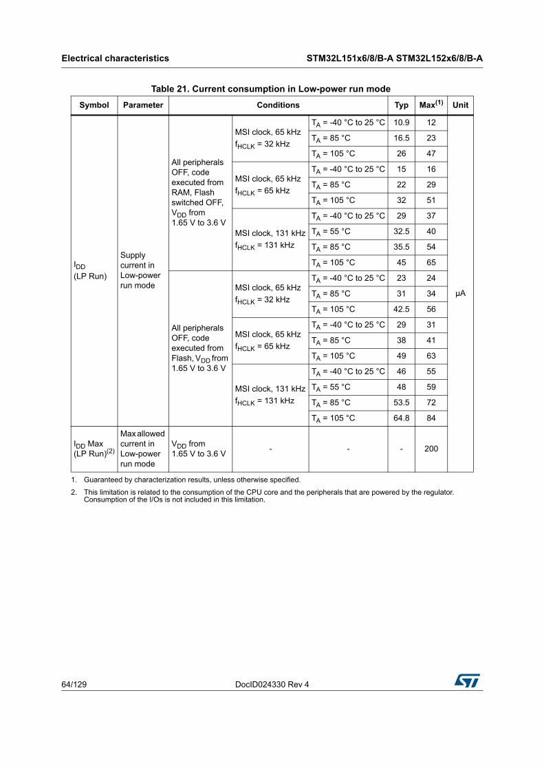
Electrical characteristics STM32L151x6/8/B-A STM32L152x6/8/B-A
64/129 DocID024330 Rev 4
Table 21. Current consumption in Low-power run mode
Symbol Parameter Conditions Typ Max(1) Unit
IDD
(LP Run)
Supply current in Low-power run mode
All peripherals OFF, code executed from RAM, Flash switched OFF, VDD from 1.65 V to 3.6 V
MSI clock, 65 kHz
fHCLK = 32 kHz
TA = -40 °C to 25 °C 10.9 12
µA
TA = 85 °C 16.5 23
TA = 105 °C 26 47
MSI clock, 65 kHz
fHCLK = 65 kHz
TA = -40 °C to 25 °C 15 16
TA = 85 °C 22 29
TA = 105 °C 32 51
MSI clock, 131 kHz
fHCLK = 131 kHz
TA = -40 °C to 25 °C 29 37
TA = 55 °C 32.5 40
TA = 85 °C 35.5 54
TA = 105 °C 45 65
All peripherals OFF, code executed from Flash, VDD from 1.65 V to 3.6 V
MSI clock, 65 kHz
fHCLK = 32 kHz
TA = -40 °C to 25 °C 23 24
TA = 85 °C 31 34
TA = 105 °C 42.5 56
MSI clock, 65 kHz
fHCLK = 65 kHz
TA = -40 °C to 25 °C 29 31
TA = 85 °C 38 41
TA = 105 °C 49 63
MSI clock, 131 kHz
fHCLK = 131 kHz
TA = -40 °C to 25 °C 46 55
TA = 55 °C 48 59
TA = 85 °C 53.5 72
TA = 105 °C 64.8 84
IDD Max (LP Run)(2)
Max allowed current in Low-power run mode
VDD from 1.65 V to 3.6 V
- - - 200
1. Guaranteed by characterization results, unless otherwise specified.
2. This limitation is related to the consumption of the CPU core and the peripherals that are powered by the regulator. Consumption of the I/Os is not included in this limitation.
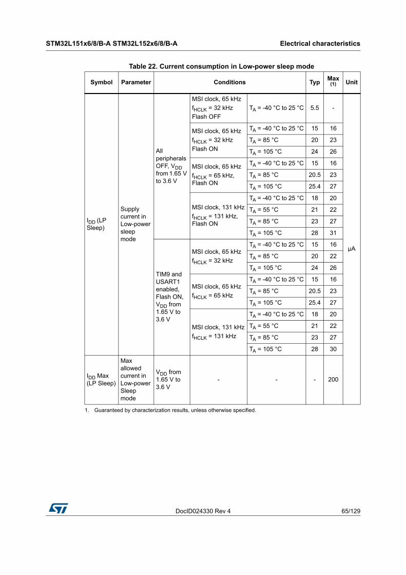
DocID024330 Rev 4 65/129
STM32L151x6/8/B-A STM32L152x6/8/B-A Electrical characteristics
105
Table 22. Current consumption in Low-power sleep mode
Symbol Parameter Conditions TypMax
(1)
1. Guaranteed by characterization results, unless otherwise specified.
Unit
IDD (LP Sleep)
Supply current in Low-power sleep mode
All peripherals OFF, VDD from 1.65 V to 3.6 V
MSI clock, 65 kHz
fHCLK = 32 kHz
Flash OFF
TA = -40 °C to 25 °C 5.5 -
µA
MSI clock, 65 kHz
fHCLK = 32 kHz
Flash ON
TA = -40 °C to 25 °C 15 16
TA = 85 °C 20 23
TA = 105 °C 24 26
MSI clock, 65 kHz
fHCLK = 65 kHz, Flash ON
TA = -40 °C to 25 °C 15 16
TA = 85 °C 20.5 23
TA = 105 °C 25.4 27
MSI clock, 131 kHz
fHCLK = 131 kHz, Flash ON
TA = -40 °C to 25 °C 18 20
TA = 55 °C 21 22
TA = 85 °C 23 27
TA = 105 °C 28 31
TIM9 and USART1 enabled, Flash ON, VDD from 1.65 V to 3.6 V
MSI clock, 65 kHz
fHCLK = 32 kHz
TA = -40 °C to 25 °C 15 16
TA = 85 °C 20 22
TA = 105 °C 24 26
MSI clock, 65 kHz
fHCLK = 65 kHz
TA = -40 °C to 25 °C 15 16
TA = 85 °C 20.5 23
TA = 105 °C 25.4 27
MSI clock, 131 kHz
fHCLK = 131 kHz
TA = -40 °C to 25 °C 18 20
TA = 55 °C 21 22
TA = 85 °C 23 27
TA = 105 °C 28 30
IDD Max (LP Sleep)
Max allowed current in Low-power Sleep mode
VDD from 1.65 V to 3.6 V
- - - 200
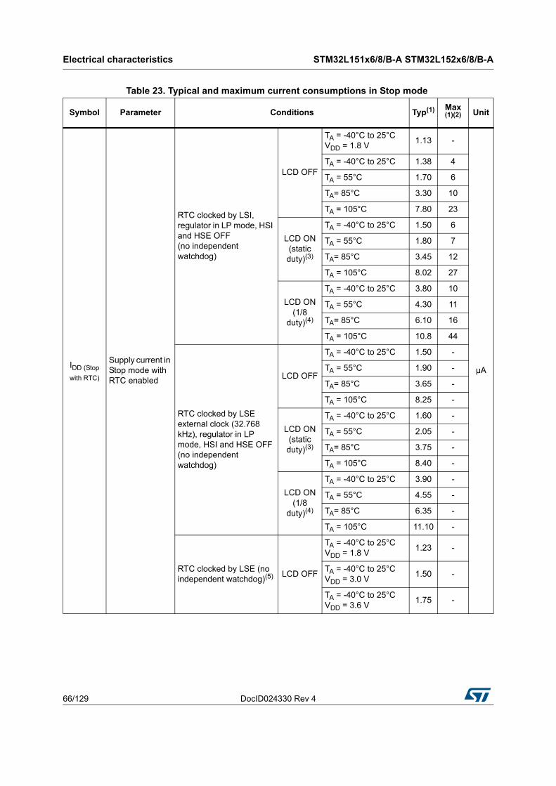
Electrical characteristics STM32L151x6/8/B-A STM32L152x6/8/B-A
66/129 DocID024330 Rev 4
Table 23. Typical and maximum current consumptions in Stop mode
Symbol Parameter Conditions Typ(1) Max(1)(2) Unit
IDD (Stop
with RTC)
Supply current in Stop mode with RTC enabled
RTC clocked by LSI, regulator in LP mode, HSI and HSE OFF (no independent watchdog)
LCD OFF
TA = -40°C to 25°C VDD = 1.8 V
1.13 -
µA
TA = -40°C to 25°C 1.38 4
TA = 55°C 1.70 6
TA= 85°C 3.30 10
TA = 105°C 7.80 23
LCD ON (static duty)(3)
TA = -40°C to 25°C 1.50 6
TA = 55°C 1.80 7
TA= 85°C 3.45 12
TA = 105°C 8.02 27
LCD ON (1/8
duty)(4)
TA = -40°C to 25°C 3.80 10
TA = 55°C 4.30 11
TA= 85°C 6.10 16
TA = 105°C 10.8 44
RTC clocked by LSE external clock (32.768 kHz), regulator in LP mode, HSI and HSE OFF (no independent watchdog)
LCD OFF
TA = -40°C to 25°C 1.50 -
TA = 55°C 1.90 -
TA= 85°C 3.65 -
TA = 105°C 8.25 -
LCD ON (static duty)(3)
TA = -40°C to 25°C 1.60 -
TA = 55°C 2.05 -
TA= 85°C 3.75 -
TA = 105°C 8.40 -
LCD ON (1/8
duty)(4)
TA = -40°C to 25°C 3.90 -
TA = 55°C 4.55 -
TA= 85°C 6.35 -
TA = 105°C 11.10 -
RTC clocked by LSE (no independent watchdog)(5) LCD OFF
TA = -40°C to 25°C VDD = 1.8 V
1.23 -
TA = -40°C to 25°C VDD = 3.0 V
1.50 -
TA = -40°C to 25°C VDD = 3.6 V
1.75 -
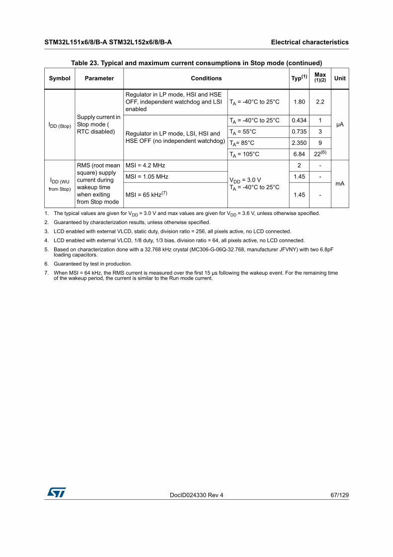
DocID024330 Rev 4 67/129
STM32L151x6/8/B-A STM32L152x6/8/B-A Electrical characteristics
105
IDD (Stop)
Supply current in Stop mode ( RTC disabled)
Regulator in LP mode, HSI and HSE OFF, independent watchdog and LSI enabled
TA = -40°C to 25°C 1.80 2.2
µA
Regulator in LP mode, LSI, HSI and HSE OFF (no independent watchdog)
TA = -40°C to 25°C 0.434 1
TA = 55°C 0.735 3
TA= 85°C 2.350 9
TA = 105°C 6.84 22(6)
IDD (WU
from Stop)
RMS (root mean square) supply current during wakeup time when exiting from Stop mode
MSI = 4.2 MHz
VDD = 3.0 V TA = -40°C to 25°C
2 -
mAMSI = 1.05 MHz 1.45 -
MSI = 65 kHz(7) 1.45 -
1. The typical values are given for VDD = 3.0 V and max values are given for VDD = 3.6 V, unless otherwise specified.
2. Guaranteed by characterization results, unless otherwise specified.
3. LCD enabled with external VLCD, static duty, division ratio = 256, all pixels active, no LCD connected.
4. LCD enabled with external VLCD, 1/8 duty, 1/3 bias, division ratio = 64, all pixels active, no LCD connected.
5. Based on characterization done with a 32.768 kHz crystal (MC306-G-06Q-32.768, manufacturer JFVNY) with two 6.8pF loading capacitors.
6. Guaranteed by test in production.
7. When MSI = 64 kHz, the RMS current is measured over the first 15 µs following the wakeup event. For the remaining time of the wakeup period, the current is similar to the Run mode current.
Table 23. Typical and maximum current consumptions in Stop mode (continued)
Symbol Parameter Conditions Typ(1) Max(1)(2) Unit
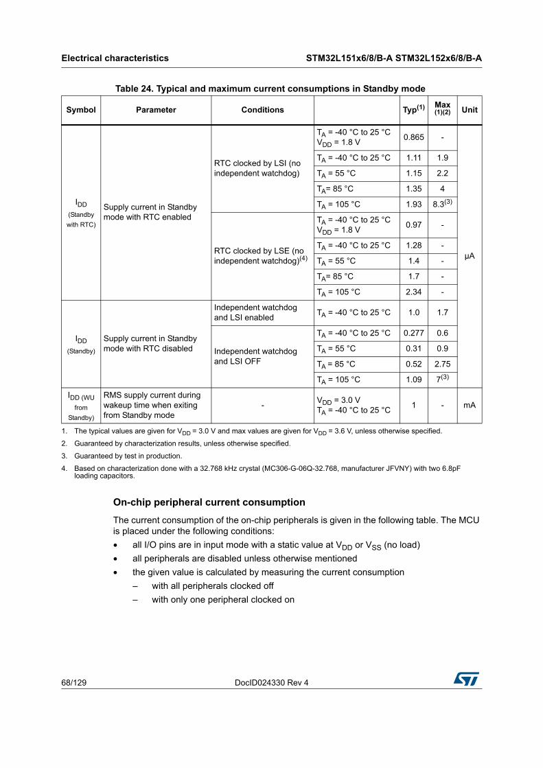
Electrical characteristics STM32L151x6/8/B-A STM32L152x6/8/B-A
68/129 DocID024330 Rev 4
On-chip peripheral current consumption
The current consumption of the on-chip peripherals is given in the following table. The MCU is placed under the following conditions:
• all I/O pins are in input mode with a static value at VDD or VSS (no load)
• all peripherals are disabled unless otherwise mentioned
• the given value is calculated by measuring the current consumption
– with all peripherals clocked off
– with only one peripheral clocked on
Table 24. Typical and maximum current consumptions in Standby mode
Symbol Parameter Conditions Typ(1) Max(1)(2) Unit
IDD
(Standby
with RTC)
Supply current in Standby mode with RTC enabled
RTC clocked by LSI (no independent watchdog)
TA = -40 °C to 25 °C VDD = 1.8 V
0.865 -
µA
TA = -40 °C to 25 °C 1.11 1.9
TA = 55 °C 1.15 2.2
TA= 85 °C 1.35 4
TA = 105 °C 1.93 8.3(3)
RTC clocked by LSE (no independent watchdog)(4)
TA = -40 °C to 25 °C VDD = 1.8 V
0.97 -
TA = -40 °C to 25 °C 1.28 -
TA = 55 °C 1.4 -
TA= 85 °C 1.7 -
TA = 105 °C 2.34 -
IDD
(Standby)
Supply current in Standby mode with RTC disabled
Independent watchdog and LSI enabled
TA = -40 °C to 25 °C 1.0 1.7
Independent watchdog and LSI OFF
TA = -40 °C to 25 °C 0.277 0.6
TA = 55 °C 0.31 0.9
TA = 85 °C 0.52 2.75
TA = 105 °C 1.09 7(3)
IDD (WU
from
Standby)
RMS supply current during wakeup time when exiting from Standby mode
-VDD = 3.0 V TA = -40 °C to 25 °C
1 - mA
1. The typical values are given for VDD = 3.0 V and max values are given for VDD = 3.6 V, unless otherwise specified.
2. Guaranteed by characterization results, unless otherwise specified.
3. Guaranteed by test in production.
4. Based on characterization done with a 32.768 kHz crystal (MC306-G-06Q-32.768, manufacturer JFVNY) with two 6.8pF loading capacitors.
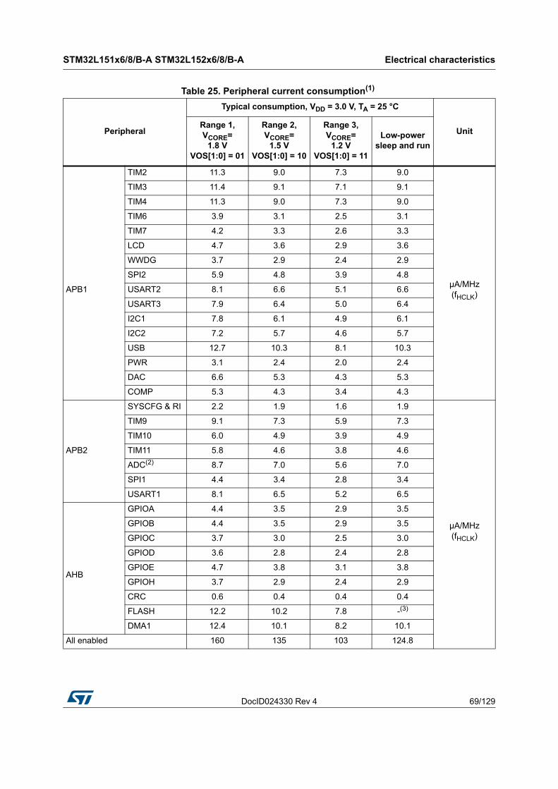
DocID024330 Rev 4 69/129
STM32L151x6/8/B-A STM32L152x6/8/B-A Electrical characteristics
105
Table 25. Peripheral current consumption(1)
Peripheral
Typical consumption, VDD = 3.0 V, TA = 25 °C
UnitRange 1, VCORE=
1.8 V VOS[1:0] = 01
Range 2, VCORE=
1.5 V VOS[1:0] = 10
Range 3, VCORE=
1.2 V VOS[1:0] = 11
Low-power sleep and run
APB1
TIM2 11.3 9.0 7.3 9.0
µA/MHz (fHCLK)
TIM3 11.4 9.1 7.1 9.1
TIM4 11.3 9.0 7.3 9.0
TIM6 3.9 3.1 2.5 3.1
TIM7 4.2 3.3 2.6 3.3
LCD 4.7 3.6 2.9 3.6
WWDG 3.7 2.9 2.4 2.9
SPI2 5.9 4.8 3.9 4.8
USART2 8.1 6.6 5.1 6.6
USART3 7.9 6.4 5.0 6.4
I2C1 7.8 6.1 4.9 6.1
I2C2 7.2 5.7 4.6 5.7
USB 12.7 10.3 8.1 10.3
PWR 3.1 2.4 2.0 2.4
DAC 6.6 5.3 4.3 5.3
COMP 5.3 4.3 3.4 4.3
APB2
SYSCFG & RI 2.2 1.9 1.6 1.9
µA/MHz (fHCLK)
TIM9 9.1 7.3 5.9 7.3
TIM10 6.0 4.9 3.9 4.9
TIM11 5.8 4.6 3.8 4.6
ADC(2) 8.7 7.0 5.6 7.0
SPI1 4.4 3.4 2.8 3.4
USART1 8.1 6.5 5.2 6.5
AHB
GPIOA 4.4 3.5 2.9 3.5
GPIOB 4.4 3.5 2.9 3.5
GPIOC 3.7 3.0 2.5 3.0
GPIOD 3.6 2.8 2.4 2.8
GPIOE 4.7 3.8 3.1 3.8
GPIOH 3.7 2.9 2.4 2.9
CRC 0.6 0.4 0.4 0.4
FLASH 12.2 10.2 7.8 -(3)
DMA1 12.4 10.1 8.2 10.1
All enabled 160 135 103 124.8
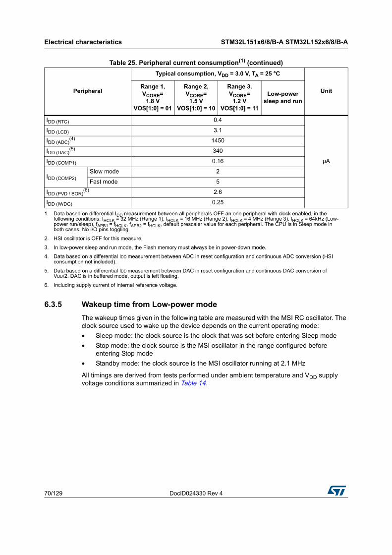
Electrical characteristics STM32L151x6/8/B-A STM32L152x6/8/B-A
70/129 DocID024330 Rev 4
6.3.5 Wakeup time from Low-power mode
The wakeup times given in the following table are measured with the MSI RC oscillator. The clock source used to wake up the device depends on the current operating mode:
• Sleep mode: the clock source is the clock that was set before entering Sleep mode
• Stop mode: the clock source is the MSI oscillator in the range configured before entering Stop mode
• Standby mode: the clock source is the MSI oscillator running at 2.1 MHz
All timings are derived from tests performed under ambient temperature and VDD supply voltage conditions summarized in Table 14.
IDD (RTC) 0.4
µA
IDD (LCD) 3.1
IDD (ADC)(4) 1450
IDD (DAC)(5) 340
IDD (COMP1) 0.16
IDD (COMP2)Slow mode 2
Fast mode 5
IDD (PVD / BOR)(6) 2.6
IDD (IWDG) 0.25
1. Data based on differential IDD measurement between all peripherals OFF an one peripheral with clock enabled, in the following conditions: fHCLK = 32 MHz (Range 1), fHCLK = 16 MHz (Range 2), fHCLK = 4 MHz (Range 3), fHCLK = 64kHz (Low-power run/sleep), fAPB1 = fHCLK, fAPB2 = fHCLK, default prescaler value for each peripheral. The CPU is in Sleep mode in both cases. No I/O pins toggling.
2. HSI oscillator is OFF for this measure.
3. In low-power sleep and run mode, the Flash memory must always be in power-down mode.
4. Data based on a differential IDD measurement between ADC in reset configuration and continuous ADC conversion (HSI consumption not included).
5. Data based on a differential IDD measurement between DAC in reset configuration and continuous DAC conversion of VDD/2. DAC is in buffered mode, output is left floating.
6. Including supply current of internal reference voltage.
Table 25. Peripheral current consumption(1) (continued)
Peripheral
Typical consumption, VDD = 3.0 V, TA = 25 °C
UnitRange 1, VCORE=
1.8 V VOS[1:0] = 01
Range 2, VCORE=
1.5 V VOS[1:0] = 10
Range 3, VCORE=
1.2 V VOS[1:0] = 11
Low-power sleep and run
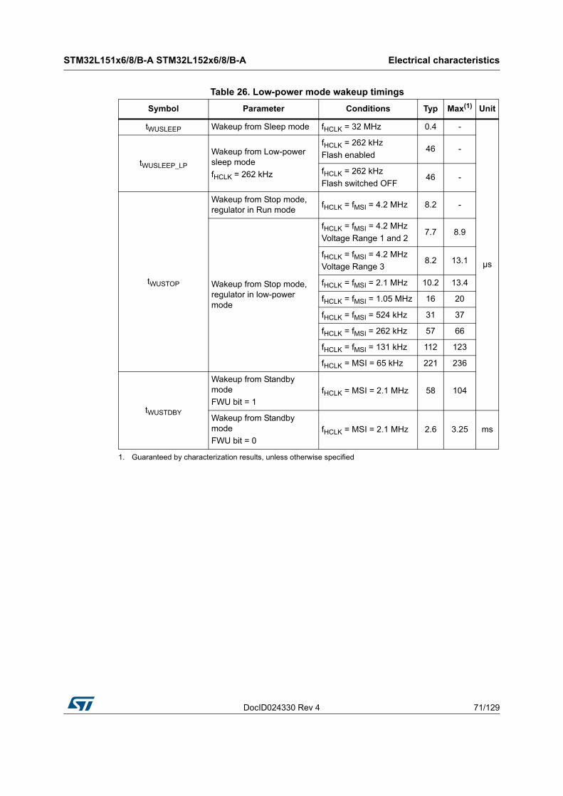
DocID024330 Rev 4 71/129
STM32L151x6/8/B-A STM32L152x6/8/B-A Electrical characteristics
105
Table 26. Low-power mode wakeup timings
Symbol Parameter Conditions Typ Max(1)
1. Guaranteed by characterization results, unless otherwise specified
Unit
tWUSLEEP Wakeup from Sleep mode fHCLK = 32 MHz 0.4 -
µs
tWUSLEEP_LP
Wakeup from Low-power sleep mode
fHCLK = 262 kHz
fHCLK = 262 kHz
Flash enabled46 -
fHCLK = 262 kHz
Flash switched OFF46 -
tWUSTOP
Wakeup from Stop mode, regulator in Run mode
fHCLK = fMSI = 4.2 MHz 8.2 -
Wakeup from Stop mode, regulator in low-power mode
fHCLK = fMSI = 4.2 MHz
Voltage Range 1 and 27.7 8.9
fHCLK = fMSI = 4.2 MHz
Voltage Range 38.2 13.1
fHCLK = fMSI = 2.1 MHz 10.2 13.4
fHCLK = fMSI = 1.05 MHz 16 20
fHCLK = fMSI = 524 kHz 31 37
fHCLK = fMSI = 262 kHz 57 66
fHCLK = fMSI = 131 kHz 112 123
fHCLK = MSI = 65 kHz 221 236
tWUSTDBY
Wakeup from Standby mode
FWU bit = 1fHCLK = MSI = 2.1 MHz 58 104
Wakeup from Standby mode
FWU bit = 0fHCLK = MSI = 2.1 MHz 2.6 3.25 ms
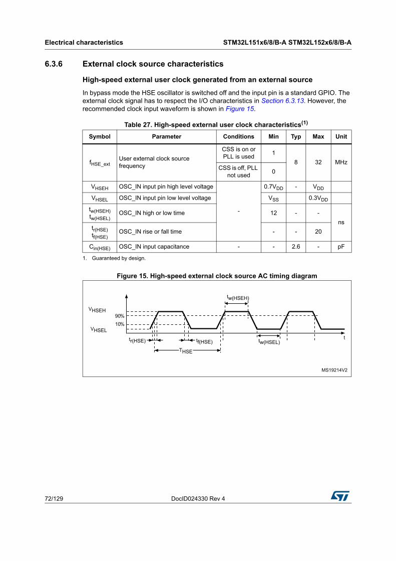
Electrical characteristics STM32L151x6/8/B-A STM32L152x6/8/B-A
72/129 DocID024330 Rev 4
6.3.6 External clock source characteristics
High-speed external user clock generated from an external source
In bypass mode the HSE oscillator is switched off and the input pin is a standard GPIO. The external clock signal has to respect the I/O characteristics in Section 6.3.13. However, the recommended clock input waveform is shown in Figure 15.
Figure 15. High-speed external clock source AC timing diagram
Table 27. High-speed external user clock characteristics(1)
1. Guaranteed by design.
Symbol Parameter Conditions Min Typ Max Unit
fHSE_extUser external clock source frequency
CSS is on or PLL is used
1
8 32 MHzCSS is off, PLL
not used0
VHSEH OSC_IN input pin high level voltage
-
0.7VDD - VDD
VHSEL OSC_IN input pin low level voltage VSS 0.3VDD
tw(HSEH)tw(HSEL)
OSC_IN high or low time 12 - -
nstr(HSE)tf(HSE)
OSC_IN rise or fall time - - 20
Cin(HSE) OSC_IN input capacitance - - 2.6 - pF
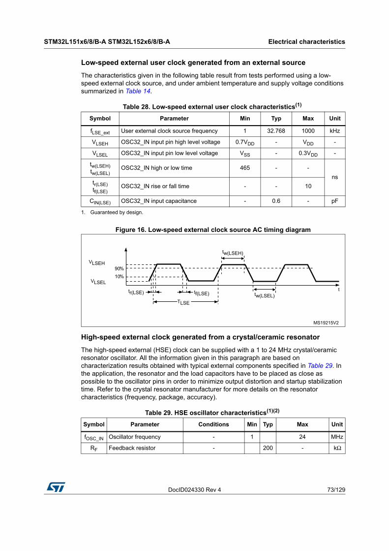
DocID024330 Rev 4 73/129
STM32L151x6/8/B-A STM32L152x6/8/B-A Electrical characteristics
105
Low-speed external user clock generated from an external source
The characteristics given in the following table result from tests performed using a low-speed external clock source, and under ambient temperature and supply voltage conditions summarized in Table 14.
Figure 16. Low-speed external clock source AC timing diagram
High-speed external clock generated from a crystal/ceramic resonator
The high-speed external (HSE) clock can be supplied with a 1 to 24 MHz crystal/ceramic resonator oscillator. All the information given in this paragraph are based on characterization results obtained with typical external components specified in Table 29. In the application, the resonator and the load capacitors have to be placed as close as possible to the oscillator pins in order to minimize output distortion and startup stabilization time. Refer to the crystal resonator manufacturer for more details on the resonator characteristics (frequency, package, accuracy).
Table 28. Low-speed external user clock characteristics(1)
1. Guaranteed by design.
Symbol Parameter Min Typ Max Unit
fLSE_ext User external clock source frequency 1 32.768 1000 kHz
VLSEH OSC32_IN input pin high level voltage 0.7VDD - VDD -
VLSEL OSC32_IN input pin low level voltage VSS - 0.3VDD -
tw(LSEH)tw(LSEL)
OSC32_IN high or low time 465 - -
nstr(LSE)tf(LSE)
OSC32_IN rise or fall time - - 10
CIN(LSE) OSC32_IN input capacitance - 0.6 - pF
Table 29. HSE oscillator characteristics(1)(2)
Symbol Parameter Conditions Min Typ Max Unit
fOSC_IN Oscillator frequency - 1 24 MHz
RF Feedback resistor - 200 - kΩ
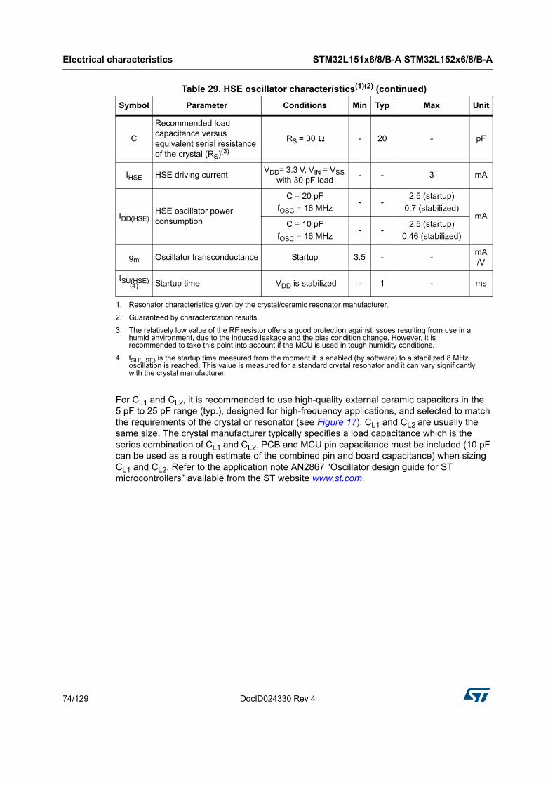
Electrical characteristics STM32L151x6/8/B-A STM32L152x6/8/B-A
74/129 DocID024330 Rev 4
For CL1 and CL2, it is recommended to use high-quality external ceramic capacitors in the 5 pF to 25 pF range (typ.), designed for high-frequency applications, and selected to match the requirements of the crystal or resonator (see Figure 17). CL1 and CL2 are usually the same size. The crystal manufacturer typically specifies a load capacitance which is the series combination of CL1 and CL2. PCB and MCU pin capacitance must be included (10 pF can be used as a rough estimate of the combined pin and board capacitance) when sizing CL1 and CL2. Refer to the application note AN2867 “Oscillator design guide for ST microcontrollers” available from the ST website www.st.com.
C
Recommended load capacitance versus equivalent serial resistance of the crystal (RS)(3)
RS = 30 Ω - 20 - pF
IHSE HSE driving currentVDD= 3.3 V, VIN = VSS
with 30 pF load- - 3 mA
IDD(HSE)HSE oscillator power consumption
C = 20 pF
fOSC = 16 MHz- -
2.5 (startup)
0.7 (stabilized)mA
C = 10 pF
fOSC = 16 MHz- -
2.5 (startup)
0.46 (stabilized)
gm Oscillator transconductance Startup 3.5 - -mA /V
tSU(HSE)(4) Startup time VDD is stabilized - 1 - ms
1. Resonator characteristics given by the crystal/ceramic resonator manufacturer.
2. Guaranteed by characterization results.
3. The relatively low value of the RF resistor offers a good protection against issues resulting from use in a humid environment, due to the induced leakage and the bias condition change. However, it is recommended to take this point into account if the MCU is used in tough humidity conditions.
4. tSU(HSE) is the startup time measured from the moment it is enabled (by software) to a stabilized 8 MHz oscillation is reached. This value is measured for a standard crystal resonator and it can vary significantly with the crystal manufacturer.
Table 29. HSE oscillator characteristics(1)(2) (continued)
Symbol Parameter Conditions Min Typ Max Unit
DocID024330 Rev 4 75/129
STM32L151x6/8/B-A STM32L152x6/8/B-A Electrical characteristics
105
Figure 17. HSE oscillator circuit diagram
1. REXT value depends on the crystal characteristics.
Low-speed external clock generated from a crystal/ceramic resonator
The low-speed external (LSE) clock can be supplied with a 32.768 kHz crystal/ceramic resonator oscillator. All the information given in this paragraph are based on characterization results obtained with typical external components specified in Table 14. In the application, the resonator and the load capacitors have to be placed as close as possible to the oscillator pins in order to minimize output distortion and startup stabilization time. Refer to the crystal resonator manufacturer for more details on the resonator characteristics (frequency, package, accuracy).
Table 30. LSE oscillator characteristics (fLSE = 32.768 kHz)(1)
1. Guaranteed by characterization results.
Symbol Parameter Conditions Min Typ Max Unit
fLSELow speed external oscillator frequency
- - 32.768 - kHz
RF Feedback resistor - - 1.2 - MΩ
C(2)
2. Refer to the note and caution paragraphs below the table, and to the application note AN2867 “Oscillator design guide for ST microcontrollers”.
Recommended load capacitance versus equivalent serial resistance of the crystal (RS)(3)
3. The oscillator selection can be optimized in terms of supply current using an high quality resonator with small RS value for example MSIV-TIN32.768kHz. Refer to crystal manufacturer for more details.
RS = 30 kΩ - 8 - pF
ILSE LSE driving current VDD = 3.3 V, VIN = VSS - - 1.1 µA
IDD (LSE)LSE oscillator current consumption
VDD = 1.8 V - 450 -
nAVDD = 3.0 V - 600 -
VDD = 3.6V - 750 -
gm Oscillator transconductance - 3 - - µA/V
tSU(LSE)(4)
4. tSU(LSE) is the startup time measured from the moment it is enabled (by software) to a stabilized 32.768 kHz oscillation is reached. This value is measured for a standard crystal resonator and it can vary significantly with the crystal manufacturer.
Startup time VDD is stabilized - 1 - s
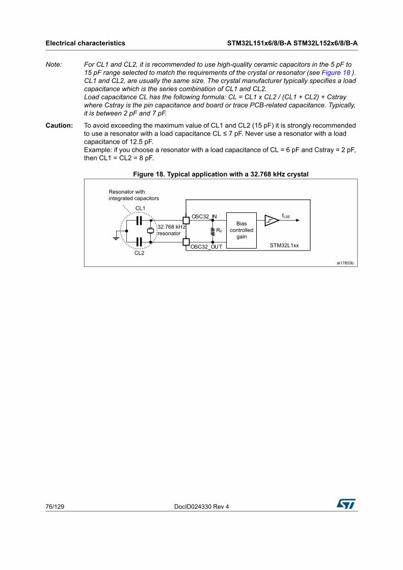
Electrical characteristics STM32L151x6/8/B-A STM32L152x6/8/B-A
76/129 DocID024330 Rev 4
Note: For CL1 and CL2, it is recommended to use high-quality ceramic capacitors in the 5 pF to 15 pF range selected to match the requirements of the crystal or resonator (see Figure 18 ). CL1 and CL2, are usually the same size. The crystal manufacturer typically specifies a load capacitance which is the series combination of CL1 and CL2. Load capacitance CL has the following formula: CL = CL1 x CL2 / (CL1 + CL2) + Cstray where Cstray is the pin capacitance and board or trace PCB-related capacitance. Typically, it is between 2 pF and 7 pF.
Caution: To avoid exceeding the maximum value of CL1 and CL2 (15 pF) it is strongly recommended to use a resonator with a load capacitance CL ≤ 7 pF. Never use a resonator with a load capacitance of 12.5 pF. Example: if you choose a resonator with a load capacitance of CL = 6 pF and Cstray = 2 pF, then CL1 = CL2 = 8 pF.
Figure 18. Typical application with a 32.768 kHz crystal
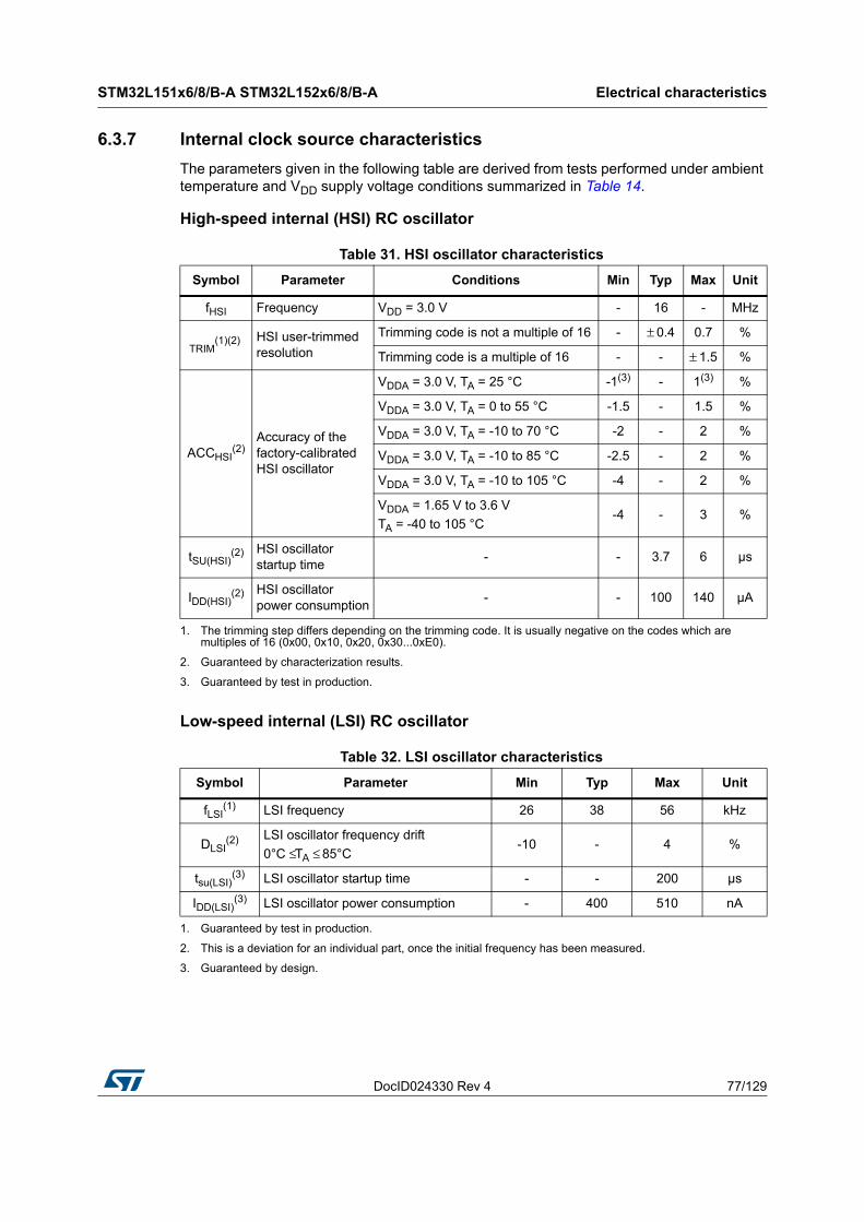
DocID024330 Rev 4 77/129
STM32L151x6/8/B-A STM32L152x6/8/B-A Electrical characteristics
105
6.3.7 Internal clock source characteristics
The parameters given in the following table are derived from tests performed under ambient temperature and VDD supply voltage conditions summarized in Table 14.
High-speed internal (HSI) RC oscillator
Low-speed internal (LSI) RC oscillator
Table 31. HSI oscillator characteristics
Symbol Parameter Conditions Min Typ Max Unit
fHSI Frequency VDD = 3.0 V - 16 - MHz
TRIM(1)(2)
1. The trimming step differs depending on the trimming code. It is usually negative on the codes which are multiples of 16 (0x00, 0x10, 0x20, 0x30...0xE0).
HSI user-trimmed resolution
Trimming code is not a multiple of 16 - ± 0.4 0.7 %
Trimming code is a multiple of 16 - - ± 1.5 %
ACCHSI(2)
2. Guaranteed by characterization results.
Accuracy of the factory-calibrated HSI oscillator
VDDA = 3.0 V, TA = 25 °C -1(3)
3. Guaranteed by test in production.
- 1(3) %
VDDA = 3.0 V, TA = 0 to 55 °C -1.5 - 1.5 %
VDDA = 3.0 V, TA = -10 to 70 °C -2 - 2 %
VDDA = 3.0 V, TA = -10 to 85 °C -2.5 - 2 %
VDDA = 3.0 V, TA = -10 to 105 °C -4 - 2 %
VDDA = 1.65 V to 3.6 V
TA = -40 to 105 °C-4 - 3 %
tSU(HSI)(2) HSI oscillator
startup time- - 3.7 6 µs
IDD(HSI)(2) HSI oscillator
power consumption- - 100 140 µA
Table 32. LSI oscillator characteristics
Symbol Parameter Min Typ Max Unit
fLSI(1)
1. Guaranteed by test in production.
LSI frequency 26 38 56 kHz
DLSI(2)
2. This is a deviation for an individual part, once the initial frequency has been measured.
LSI oscillator frequency drift
0°C ≤ TA ≤ 85°C-10 - 4 %
tsu(LSI)(3)
3. Guaranteed by design.
LSI oscillator startup time - - 200 µs
IDD(LSI)(3) LSI oscillator power consumption - 400 510 nA
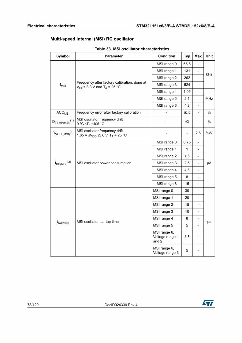
Electrical characteristics STM32L151x6/8/B-A STM32L152x6/8/B-A
78/129 DocID024330 Rev 4
Multi-speed internal (MSI) RC oscillator
Table 33. MSI oscillator characteristics
Symbol Parameter Condition Typ Max Unit
fMSIFrequency after factory calibration, done at VDD= 3.3 V and TA = 25 °C
MSI range 0 65.5 -
kHz MSI range 1 131 -
MSI range 2 262 -
MSI range 3 524 -
MSI range 4 1.05 -
MHzMSI range 5 2.1 -
MSI range 6 4.2 -
ACCMSI Frequency error after factory calibration - ±0.5 - %
DTEMP(MSI)(1) MSI oscillator frequency drift
0 °C ≤ TA ≤ 105 °C- ±3 - %
DVOLT(MSI)(1) MSI oscillator frequency drift
1.65 V ≤ VDD ≤ 3.6 V, TA = 25 °C- - 2.5 %/V
IDD(MSI)(2) MSI oscillator power consumption
MSI range 0 0.75 -
µA
MSI range 1 1 -
MSI range 2 1.5 -
MSI range 3 2.5 -
MSI range 4 4.5 -
MSI range 5 8 -
MSI range 6 15 -
tSU(MSI) MSI oscillator startup time
MSI range 0 30 -
µs
MSI range 1 20 -
MSI range 2 15 -
MSI range 3 10 -
MSI range 4 6 -
MSI range 5 5 -
MSI range 6, Voltage range 1 and 2
3.5 -
MSI range 6, Voltage range 3
5 -
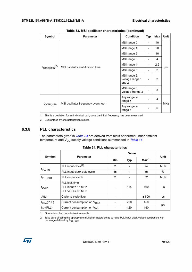
DocID024330 Rev 4 79/129
STM32L151x6/8/B-A STM32L152x6/8/B-A Electrical characteristics
105
6.3.8 PLL characteristics
The parameters given in Table 34 are derived from tests performed under ambient temperature and VDD supply voltage conditions summarized in Table 14.
tSTAB(MSI)(2) MSI oscillator stabilization time
MSI range 0 - 40
µs
MSI range 1 - 20
MSI range 2 - 10
MSI range 3 - 4
MSI range 4 - 2.5
MSI range 5 - 2
MSI range 6, Voltage range 1 and 2
- 2
MSI range 3, Voltage Range 3
- 3
fOVER(MSI) MSI oscillator frequency overshoot
Any range to range 5
- 4
MHzAny range to range 6
- 6
1. This is a deviation for an individual part, once the initial frequency has been measured.
2. Guaranteed by characterization results.
Table 33. MSI oscillator characteristics (continued)
Symbol Parameter Condition Typ Max Unit
Table 34. PLL characteristics
Symbol ParameterValue
UnitMin Typ Max(1)
1. Guaranteed by characterization results.
fPLL_IN
PLL input clock(2)
2. Take care of using the appropriate multiplier factors so as to have PLL input clock values compatible with the range defined by fPLL_OUT.
2 - 24 MHz
PLL input clock duty cycle 45 - 55 %
fPLL_OUT PLL output clock 2 - 32 MHz
tLOCK
PLL lock time
PLL input = 16 MHz
PLL VCO = 96 MHz
- 115 160 µs
Jitter Cycle-to-cycle jitter - - ± 600 ps
IDDA(PLL) Current consumption on VDDA - 220 450µA
IDD(PLL) Current consumption on VDD - 120 150
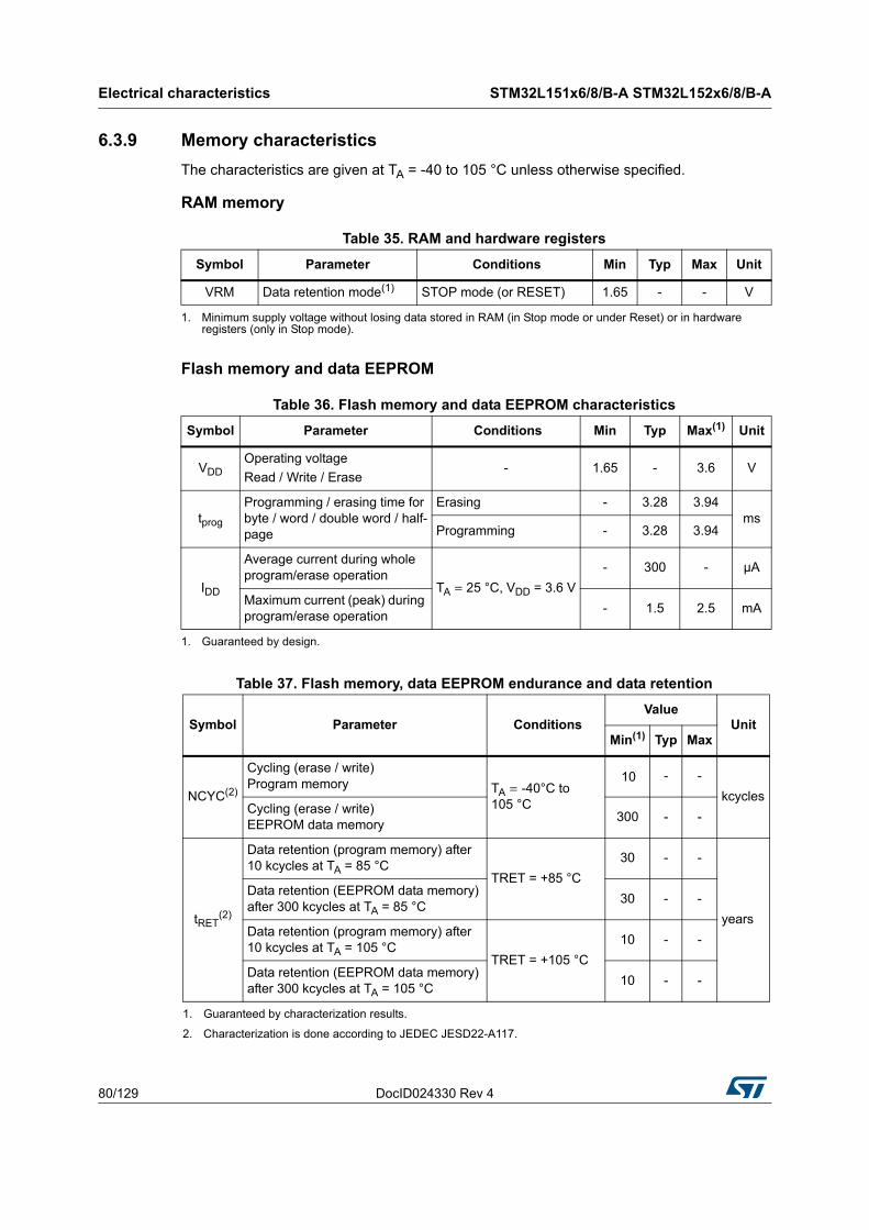
Electrical characteristics STM32L151x6/8/B-A STM32L152x6/8/B-A
80/129 DocID024330 Rev 4
6.3.9 Memory characteristics
The characteristics are given at TA = -40 to 105 °C unless otherwise specified.
RAM memory
Flash memory and data EEPROM
Table 35. RAM and hardware registers
Symbol Parameter Conditions Min Typ Max Unit
VRM Data retention mode(1)
1. Minimum supply voltage without losing data stored in RAM (in Stop mode or under Reset) or in hardware registers (only in Stop mode).
STOP mode (or RESET) 1.65 - - V
Table 36. Flash memory and data EEPROM characteristics
Symbol Parameter Conditions Min Typ Max(1)
1. Guaranteed by design.
Unit
VDDOperating voltage
Read / Write / Erase- 1.65 - 3.6 V
tprog
Programming / erasing time for byte / word / double word / half-page
Erasing - 3.28 3.94ms
Programming - 3.28 3.94
IDD
Average current during whole program/erase operation
TA = 25 °C, VDD = 3.6 V
- 300 - µA
Maximum current (peak) during program/erase operation
- 1.5 2.5 mA
Table 37. Flash memory, data EEPROM endurance and data retention
Symbol Parameter ConditionsValue
UnitMin(1)
1. Guaranteed by characterization results.
Typ Max
NCYC(2)
Cycling (erase / write) Program memory TA = -40°C to
105 °C
10 - -
kcyclesCycling (erase / write) EEPROM data memory
300 - -
tRET(2)
2. Characterization is done according to JEDEC JESD22-A117.
Data retention (program memory) after 10 kcycles at TA = 85 °C
TRET = +85 °C
30 - -
years
Data retention (EEPROM data memory) after 300 kcycles at TA = 85 °C
30 - -
Data retention (program memory) after 10 kcycles at TA = 105 °C
TRET = +105 °C
10 - -
Data retention (EEPROM data memory) after 300 kcycles at TA = 105 °C
10 - -
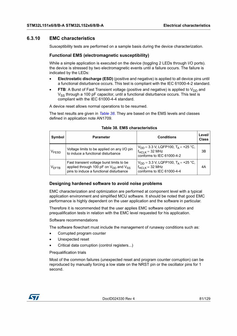
DocID024330 Rev 4 81/129
STM32L151x6/8/B-A STM32L152x6/8/B-A Electrical characteristics
105
6.3.10 EMC characteristics
Susceptibility tests are performed on a sample basis during the device characterization.
Functional EMS (electromagnetic susceptibility)
While a simple application is executed on the device (toggling 2 LEDs through I/O ports). the device is stressed by two electromagnetic events until a failure occurs. The failure is indicated by the LEDs:
• Electrostatic discharge (ESD) (positive and negative) is applied to all device pins until a functional disturbance occurs. This test is compliant with the IEC 61000-4-2 standard.
• FTB: A Burst of Fast Transient voltage (positive and negative) is applied to VDD and VSS through a 100 pF capacitor, until a functional disturbance occurs. This test is compliant with the IEC 61000-4-4 standard.
A device reset allows normal operations to be resumed.
The test results are given in Table 38. They are based on the EMS levels and classes defined in application note AN1709.
Designing hardened software to avoid noise problems
EMC characterization and optimization are performed at component level with a typical application environment and simplified MCU software. It should be noted that good EMC performance is highly dependent on the user application and the software in particular.
Therefore it is recommended that the user applies EMC software optimization and prequalification tests in relation with the EMC level requested for his application.
Software recommendations
The software flowchart must include the management of runaway conditions such as:
• Corrupted program counter
• Unexpected reset
• Critical data corruption (control registers...)
Prequalification trials
Most of the common failures (unexpected reset and program counter corruption) can be reproduced by manually forcing a low state on the NRST pin or the oscillator pins for 1 second.
Table 38. EMS characteristics
Symbol Parameter ConditionsLevel/Class
VFESDVoltage limits to be applied on any I/O pin to induce a functional disturbance
VDD = 3.3 V, LQFP100, TA = +25 °C, fHCLK = 32 MHz conforms to IEC 61000-4-2
3B
VEFTB
Fast transient voltage burst limits to be applied through 100 pF on VDD and VSS pins to induce a functional disturbance
VDD = 3.3 V, LQFP100, TA = +25 °C, fHCLK = 32 MHz conforms to IEC 61000-4-4
4A
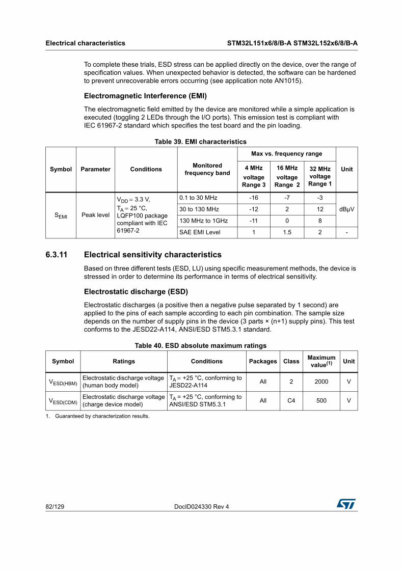
Electrical characteristics STM32L151x6/8/B-A STM32L152x6/8/B-A
82/129 DocID024330 Rev 4
To complete these trials, ESD stress can be applied directly on the device, over the range of specification values. When unexpected behavior is detected, the software can be hardened to prevent unrecoverable errors occurring (see application note AN1015).
Electromagnetic Interference (EMI)
The electromagnetic field emitted by the device are monitored while a simple application is executed (toggling 2 LEDs through the I/O ports). This emission test is compliant with IEC 61967-2 standard which specifies the test board and the pin loading.
6.3.11 Electrical sensitivity characteristics
Based on three different tests (ESD, LU) using specific measurement methods, the device is stressed in order to determine its performance in terms of electrical sensitivity.
Electrostatic discharge (ESD)
Electrostatic discharges (a positive then a negative pulse separated by 1 second) are applied to the pins of each sample according to each pin combination. The sample size depends on the number of supply pins in the device (3 parts × (n+1) supply pins). This test conforms to the JESD22-A114, ANSI/ESD STM5.3.1 standard.
Table 39. EMI characteristics
Symbol Parameter ConditionsMonitored
frequency band
Max vs. frequency range
Unit4 MHz
voltage Range 3
16 MHz
voltage Range 2
32 MHz voltage Range 1
SEMI Peak level
VDD = 3.3 V,
TA = 25 °C, LQFP100 package compliant with IEC 61967-2
0.1 to 30 MHz -16 -7 -3
dBµV30 to 130 MHz -12 2 12
130 MHz to 1GHz -11 0 8
SAE EMI Level 1 1.5 2 -
Table 40. ESD absolute maximum ratings
Symbol Ratings Conditions Packages ClassMaximum value(1) Unit
VESD(HBM)Electrostatic discharge voltage (human body model)
TA = +25 °C, conforming to JESD22-A114
All 2 2000 V
VESD(CDM)Electrostatic discharge voltage (charge device model)
TA = +25 °C, conforming to ANSI/ESD STM5.3.1
All C4 500 V
1. Guaranteed by characterization results.
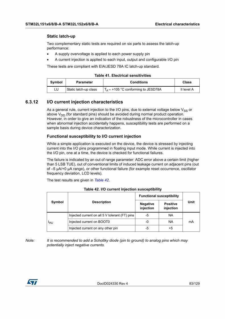
DocID024330 Rev 4 83/129
STM32L151x6/8/B-A STM32L152x6/8/B-A Electrical characteristics
105
Static latch-up
Two complementary static tests are required on six parts to assess the latch-up performance:
• A supply overvoltage is applied to each power supply pin
• A current injection is applied to each input, output and configurable I/O pin
These tests are compliant with EIA/JESD 78A IC latch-up standard.
6.3.12 I/O current injection characteristics
As a general rule, current injection to the I/O pins, due to external voltage below VSS or above VDD (for standard pins) should be avoided during normal product operation. However, in order to give an indication of the robustness of the microcontroller in cases when abnormal injection accidentally happens, susceptibility tests are performed on a sample basis during device characterization.
Functional susceptibility to I/O current injection
While a simple application is executed on the device, the device is stressed by injecting current into the I/O pins programmed in floating input mode. While current is injected into the I/O pin, one at a time, the device is checked for functional failures.
The failure is indicated by an out of range parameter: ADC error above a certain limit (higher than 5 LSB TUE), out of conventional limits of induced leakage current on adjacent pins (out of –5 µA/+0 µA range), or other functional failure (for example reset occurrence, oscillator frequency deviation, LCD levels).
The test results are given in Table 42.
Note: It is recommended to add a Schottky diode (pin to ground) to analog pins which may potentially inject negative currents.
Table 41. Electrical sensitivities
Symbol Parameter Conditions Class
LU Static latch-up class TA = +105 °C conforming to JESD78A II level A
Table 42. I/O current injection susceptibility
Symbol Description
Functional susceptibility
UnitNegative injection
Positive injection
IINJ
Injected current on all 5 V tolerant (FT) pins -5 NA
mAInjected current on BOOT0 -0 NA
Injected current on any other pin -5 +5
Electrical characteristics STM32L151x6/8/B-A STM32L152x6/8/B-A
84/129 DocID024330 Rev 4
6.3.13 I/O port characteristics
General input/output characteristics
Unless otherwise specified, the parameters given in Table 43 are derived from tests performed under conditions summarized in Table 14. All I/Os are CMOS and TTL compliant.
Table 43. I/O static characteristics
Symbol Parameter Conditions Min Typ Max Unit
VIL Input low level voltageTC and FT I/O - - 0.3 VDD
(1)(2)
V
BOOT0 - 0.14 VDD(2)
VIH Input high level voltage
TC I/O 0.45 VDD+0.38(2) - -
FT I/O 0.39 VDD+0.59(2) - -
BOOT0 0.15 VDD+0.56(2) - -
VhysI/O Schmitt trigger voltage hysteresis(2)
TC and FT I/O - 10% VDD(3) -
BOOT0 - 0.01 -
Ilkg Input leakage current(4)
VSS ≤ VIN ≤ VDDI/Os with LCD
- - ±50
nA
VSS ≤ VIN ≤ VDDI/Os with analog
switches- - ±50
VSS ≤ VIN ≤ VDDI/Os with analog
switches and LCD- - ±50
VSS ≤ VIN ≤ VDDI/Os with USB
- - ±250
VSS ≤ VIN ≤ VDDTC and FT I/O
- - ±50
FT I/O
VDD ≤ VIN ≤ 5V- - ±10 uA
RPUWeak pull-up equivalent resistor(5)(1) VIN = VSS 30 45 60 kΩ
RPDWeak pull-down equivalent resistor(5) VIN = VDD 30 45 60 kΩ
CIO I/O pin capacitance - - 5 - pF
1. Guaranteed by test in production.
2. Guaranteed by design.
3. With a minimum of 200 mV.
4. The max. value may be exceeded if negative current is injected on adjacent pins.
5. Pull-up and pull-down resistors are designed with a true resistance in series with a switchable PMOS/NMOS. This PMOS/NMOS contribution to the series resistance is minimal (~10% order).
DocID024330 Rev 4 85/129
STM32L151x6/8/B-A STM32L152x6/8/B-A Electrical characteristics
105
Output driving current
The GPIOs (general purpose input/outputs) can sink or source up to ±8 mA, and sink or source up to ±20 mA (with the non-standard VOL/VOH specifications given in Table 44.
In the user application, the number of I/O pins which can drive current must be limited to respect the absolute maximum rating specified in Section 6.2:
• The sum of the currents sourced by all the I/Os on VDD, plus the maximum Run consumption of the MCU sourced on VDD, cannot exceed the absolute maximum rating ΣIVDD (see Table 12).
• The sum of the currents sunk by all the I/Os on VSS plus the maximum Run consumption of the MCU sunk on VSS cannot exceed the absolute maximum rating ΣIVSS (see Table 12).
Output voltage levels
Unless otherwise specified, the parameters given in Table 44 are derived from tests performed under ambient temperature and VDD supply voltage conditions summarized in Table 14. All I/Os are CMOS and TTL compliant.
Table 44. Output voltage characteristics
Symbol Parameter Conditions Min Max Unit
VOL(1)(2) Output low level voltage for an I/O pin IIO = 8 mA
2.7 V < VDD < 3.6 V
- 0.4
V
VOH(3)(2) Output high level voltage for an I/O pin VDD-0.4 -
VOL (1)(4) Output low level voltage for an I/O pin IIO = 4 mA
1.65 V < VDD < 2.7 V
- 0.45
VOH (3)(4) Output high level voltage for an I/O pin VDD-0.45 -
VOL(1)(4) Output low level voltage for an I/O pin IIO = 15 mA
2.7 V < VDD < 3.6 V
- 1.3
VOH(3)(4) Output high level voltage for an I/O pin VDD-1.3 -
1. The IIO current sunk by the device must always respect the absolute maximum rating specified in Table 12 and the sum of IIO (I/O ports and control pins) must not exceed IVSS.
2. Guaranteed by test in production.
3. The IIO current sourced by the device must always respect the absolute maximum rating specified in Table 12 and the sum of IIO (I/O ports and control pins) must not exceed IVDD.
4. Guaranteed by characterization results.
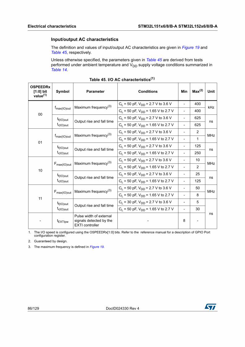
Electrical characteristics STM32L151x6/8/B-A STM32L152x6/8/B-A
86/129 DocID024330 Rev 4
Input/output AC characteristics
The definition and values of input/output AC characteristics are given in Figure 19 and Table 45, respectively.
Unless otherwise specified, the parameters given in Table 45 are derived from tests performed under ambient temperature and VDD supply voltage conditions summarized in Table 14.
Table 45. I/O AC characteristics(1)
OSPEEDRx[1:0] bit value(1)
Symbol Parameter Conditions Min Max(2) Unit
00
fmax(IO)out Maximum frequency(3)CL = 50 pF, VDD = 2.7 V to 3.6 V - 400
kHzCL = 50 pF, VDD = 1.65 V to 2.7 V - 400
tf(IO)out
tr(IO)outOutput rise and fall time
CL = 50 pF, VDD = 2.7 V to 3.6 V - 625ns
CL = 50 pF, VDD = 1.65 V to 2.7 V - 625
01
fmax(IO)out Maximum frequency(3)CL = 50 pF, VDD = 2.7 V to 3.6 V - 2
MHzCL = 50 pF, VDD = 1.65 V to 2.7 V - 1
tf(IO)out
tr(IO)outOutput rise and fall time
CL = 50 pF, VDD = 2.7 V to 3.6 V - 125ns
CL = 50 pF, VDD = 1.65 V to 2.7 V - 250
10
Fmax(IO)out Maximum frequency(3)CL = 50 pF, VDD = 2.7 V to 3.6 V - 10
MHzCL = 50 pF, VDD = 1.65 V to 2.7 V - 2
tf(IO)out
tr(IO)outOutput rise and fall time
CL = 50 pF, VDD = 2.7 V to 3.6 V - 25ns
CL = 50 pF, VDD = 1.65 V to 2.7 V - 125
11
Fmax(IO)out Maximum frequency(3)CL = 50 pF, VDD = 2.7 V to 3.6 V - 50
MHzCL = 50 pF, VDD = 1.65 V to 2.7 V - 8
tf(IO)out
tr(IO)outOutput rise and fall time
CL = 30 pF, VDD = 2.7 V to 3.6 V - 5
nsCL = 50 pF, VDD = 1.65 V to 2.7 V - 30
- tEXTIpw
Pulse width of external signals detected by the EXTI controller
- 8 -
1. The I/O speed is configured using the OSPEEDRx[1:0] bits. Refer to the reference manual for a description of GPIO Port configuration register.
2. Guaranteed by design.
3. The maximum frequency is defined in Figure 19.
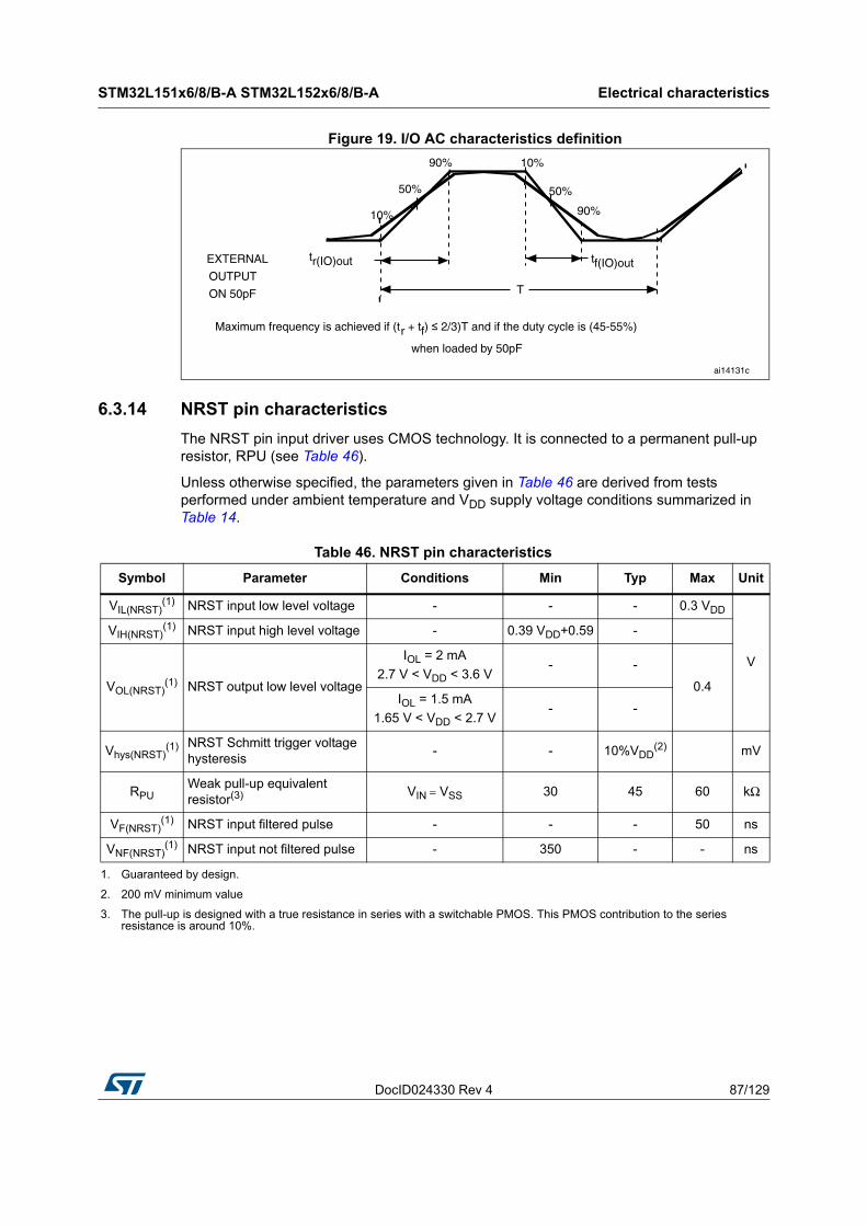
DocID024330 Rev 4 87/129
STM32L151x6/8/B-A STM32L152x6/8/B-A Electrical characteristics
105
Figure 19. I/O AC characteristics definition
6.3.14 NRST pin characteristics
The NRST pin input driver uses CMOS technology. It is connected to a permanent pull-up resistor, RPU (see Table 46).
Unless otherwise specified, the parameters given in Table 46 are derived from tests performed under ambient temperature and VDD supply voltage conditions summarized in Table 14.
Table 46. NRST pin characteristics
Symbol Parameter Conditions Min Typ Max Unit
VIL(NRST)(1) NRST input low level voltage - - - 0.3 VDD
V
VIH(NRST)(1) NRST input high level voltage - 0.39 VDD+0.59 -
VOL(NRST)(1) NRST output low level voltage
IOL = 2 mA
2.7 V < VDD < 3.6 V- -
0.4IOL = 1.5 mA
1.65 V < VDD < 2.7 V- -
Vhys(NRST)(1) NRST Schmitt trigger voltage
hysteresis - - 10%VDD
(2) mV
RPUWeak pull-up equivalent resistor(3) VIN = VSS 30 45 60 kΩ
VF(NRST)(1) NRST input filtered pulse - - - 50 ns
VNF(NRST)(1) NRST input not filtered pulse - 350 - - ns
1. Guaranteed by design.
2. 200 mV minimum value
3. The pull-up is designed with a true resistance in series with a switchable PMOS. This PMOS contribution to the series resistance is around 10%.
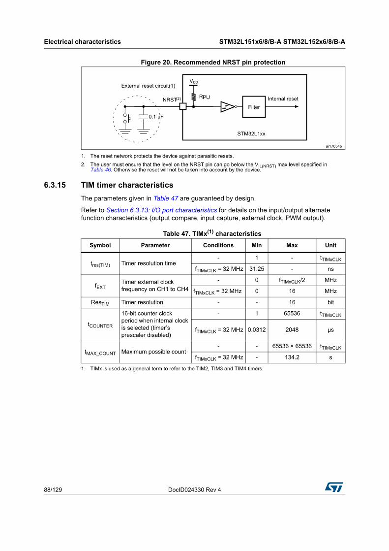
Electrical characteristics STM32L151x6/8/B-A STM32L152x6/8/B-A
88/129 DocID024330 Rev 4
Figure 20. Recommended NRST pin protection
1. The reset network protects the device against parasitic resets.
2. The user must ensure that the level on the NRST pin can go below the VIL(NRST) max level specified in Table 46. Otherwise the reset will not be taken into account by the device.
6.3.15 TIM timer characteristics
The parameters given in Table 47 are guaranteed by design.
Refer to Section 6.3.13: I/O port characteristics for details on the input/output alternate function characteristics (output compare, input capture, external clock, PWM output).
Table 47. TIMx(1) characteristics
1. TIMx is used as a general term to refer to the TIM2, TIM3 and TIM4 timers.
Symbol Parameter Conditions Min Max Unit
tres(TIM) Timer resolution time- 1 - tTIMxCLK
fTIMxCLK = 32 MHz 31.25 - ns
fEXTTimer external clock frequency on CH1 to CH4
- 0 fTIMxCLK/2 MHz
fTIMxCLK = 32 MHz 0 16 MHz
ResTIM Timer resolution - - 16 bit
tCOUNTER
16-bit counter clock period when internal clock is selected (timer’s prescaler disabled)
- 1 65536 tTIMxCLK
fTIMxCLK = 32 MHz 0.0312 2048 µs
tMAX_COUNT Maximum possible count- - 65536 × 65536 tTIMxCLK
fTIMxCLK = 32 MHz - 134.2 s
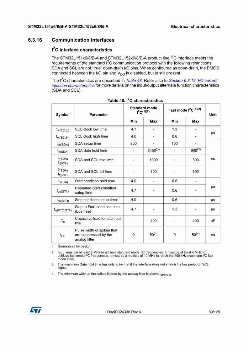
DocID024330 Rev 4 89/129
STM32L151x6/8/B-A STM32L152x6/8/B-A Electrical characteristics
105
6.3.16 Communication interfaces
I2C interface characteristics
The STM32L151x6/8/B-A and STM32L152x6/8/B-A product line I2C interface meets the requirements of the standard I2C communication protocol with the following restrictions: SDA and SCL are not “true” open-drain I/O pins. When configured as open-drain, the PMOS connected between the I/O pin and VDD is disabled, but is still present.
The I2C characteristics are described in Table 48. Refer also to Section 6.3.12: I/O current injection characteristics for more details on the input/output alternate function characteristics (SDA and SCL).
Table 48. I2C characteristics
Symbol Parameter
Standard mode I2C(1)(2)
1. Guaranteed by design.
Fast mode I2C(1)(2)
2. fPCLK1 must be at least 2 MHz to achieve standard mode I²C frequencies. It must be at least 4 MHz to achieve fast mode I²C frequencies. It must be a multiple of 10 MHz to reach the 400 kHz maximum I²C fast mode clock.
Unit
Min Max Min Max
tw(SCLL) SCL clock low time 4.7 - 1.3 -µs
tw(SCLH) SCL clock high time 4.0 - 0.6 -
tsu(SDA) SDA setup time 250 - 100 -
ns
th(SDA) SDA data hold time - 3450(3) - 900(3)
3. The maximum Data hold time has only to be met if the interface does not stretch the low period of SCL signal.
tr(SDA)tr(SCL)
SDA and SCL rise time - 1000 - 300
tf(SDA)tf(SCL)
SDA and SCL fall time - 300 - 300
th(STA) Start condition hold time 4.0 - 0.6 -
µstsu(STA)
Repeated Start condition setup time
4.7 - 0.6 -
tsu(STO) Stop condition setup time 4.0 - 0.6 - μs
tw(STO:STA)Stop to Start condition time (bus free)
4.7 - 1.3 - μs
CbCapacitive load for each bus line
- 400 - 400 pF
tSP
Pulse width of spikes that are suppressed by the analog filter
0 50(4)
4. The minimum width of the spikes filtered by the analog filter is above tSP(max).
0 50(4) ns
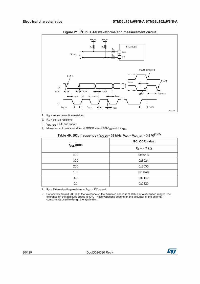
Electrical characteristics STM32L151x6/8/B-A STM32L152x6/8/B-A
90/129 DocID024330 Rev 4
Figure 21. I2C bus AC waveforms and measurement circuit
1. RS = series protection resistors
2. RP = pull-up resistors
3. VDD_I2C = I2C bus supply
4. Measurement points are done at CMOS levels: 0.3VDD and 0.7VDD.
Table 49. SCL frequency (fPCLK1= 32 MHz, VDD = VDD_I2C = 3.3 V)(1)(2)
1. RP = External pull-up resistance, fSCL = I2C speed.
2. For speeds around 200 kHz, the tolerance on the achieved speed is of ±5%. For other speed ranges, the tolerance on the achieved speed is ±2%. These variations depend on the accuracy of the external components used to design the application.
fSCL (kHz)I2C_CCR value
RP = 4.7 kΩ
400 0x801B
300 0x8024
200 0x8035
100 0x00A0
50 0x0140
20 0x0320
DocID024330 Rev 4 91/129
STM32L151x6/8/B-A STM32L152x6/8/B-A Electrical characteristics
105
SPI characteristics
Unless otherwise specified, the parameters given in the following table are derived from tests performed under ambient temperature, fPCLKx frequency and VDD supply voltage conditions summarized in Table 14.
Refer to Section 6.3.12: I/O current injection characteristics for more details on the input/output alternate function characteristics (NSS, SCK, MOSI, MISO).
Table 50. SPI characteristics(1)
1. The characteristics above are given for voltage Range 1.
Symbol Parameter Conditions Min Max(2)
2. Guaranteed by characterization results.
Unit
fSCK1/tc(SCK)
SPI clock frequency
Master mode - 16
MHzSlave mode - 16
Slave transmitter - 12(3)
3. The maximum SPI clock frequency in slave transmitter mode is given for an SPI slave input clock duty cycle (DuCy(SCK)) ranging between 40 to 60%.
tr(SCK)(2)
tf(SCK)(2)
SPI clock rise and fall time
Capacitive load: C = 30 pF - 6 ns
DuCy(SCK)SPI slave input clock duty cycle
Slave mode 30 70 %
tsu(NSS) NSS setup time Slave mode 4tHCLK -
ns
th(NSS) NSS hold time Slave mode 2tHCLK -
tw(SCKH)(2)
tw(SCKL)(2) SCK high and low time Master mode
tSCK/2−5
tSCK/2+3
tsu(MI)(2)
Data input setup timeMaster mode 5 -
tsu(SI)(2) Slave mode 6 -
th(MI)(2)
Data input hold timeMaster mode 5 -
th(SI)(2) Slave mode 5 -
ta(SO)(4)
4. Min time is for the minimum time to drive the output and max time is for the maximum time to validate the data.
Data output access time Slave mode 0 3tHCLK
tv(SO) (2) Data output valid time Slave mode - 33
tv(MO)(2) Data output valid time Master mode - 6.5
th(SO)(2)
Data output hold timeSlave mode 17 -
th(MO)(2) Master mode 0.5 -
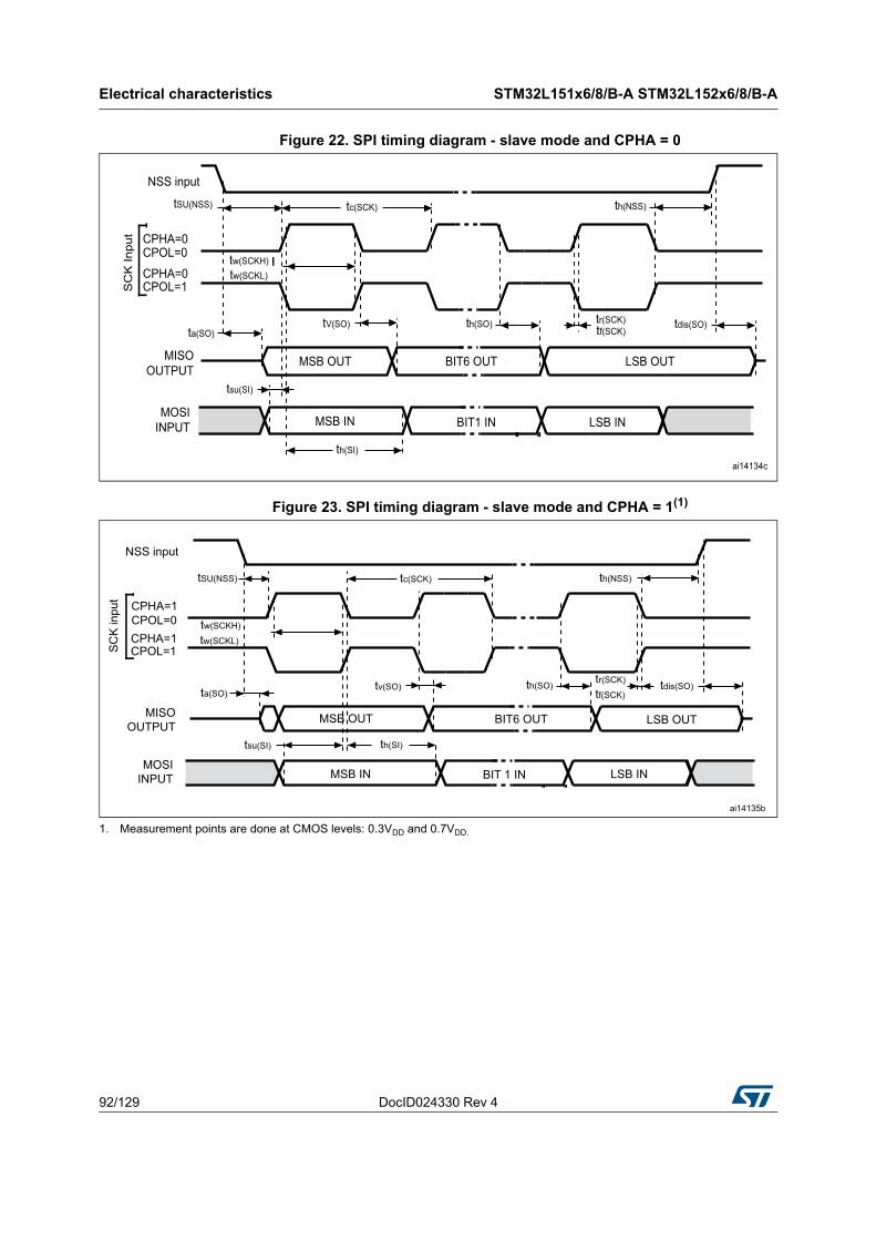
Electrical characteristics STM32L151x6/8/B-A STM32L152x6/8/B-A
92/129 DocID024330 Rev 4
Figure 22. SPI timing diagram - slave mode and CPHA = 0
Figure 23. SPI timing diagram - slave mode and CPHA = 1(1)
1. Measurement points are done at CMOS levels: 0.3VDD and 0.7VDD.
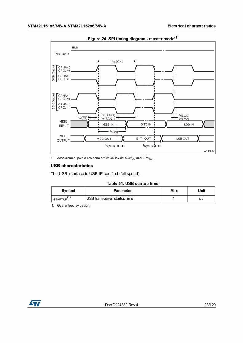
DocID024330 Rev 4 93/129
STM32L151x6/8/B-A STM32L152x6/8/B-A Electrical characteristics
105
Figure 24. SPI timing diagram - master mode(1)
1. Measurement points are done at CMOS levels: 0.3VDD and 0.7VDD.
USB characteristics
The USB interface is USB-IF certified (full speed).
Table 51. USB startup time
Symbol Parameter Max Unit
tSTARTUP(1)
1. Guaranteed by design.
USB transceiver startup time 1 µs
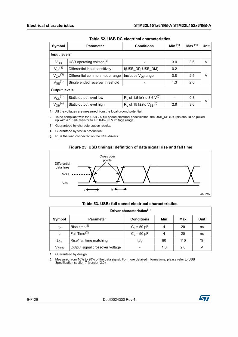
Electrical characteristics STM32L151x6/8/B-A STM32L152x6/8/B-A
94/129 DocID024330 Rev 4
Figure 25. USB timings: definition of data signal rise and fall time
Table 52. USB DC electrical characteristics
Symbol Parameter Conditions Min.(1)
1. All the voltages are measured from the local ground potential.
Max.(1) Unit
Input levels
VDD USB operating voltage(2)
2. To be compliant with the USB 2.0 full speed electrical specification, the USB_DP (D+) pin should be pulled up with a 1.5 kΩ resistor to a 3.0-to-3.6 V voltage range.
- 3.0 3.6 V
VDI(3)
3. Guaranteed by characterization results.
Differential input sensitivity I(USB_DP, USB_DM) 0.2 -
VVCM(3) Differential common mode range Includes VDI range 0.8 2.5
VSE(3) Single ended receiver threshold - 1.3 2.0
Output levels
VOL(4)
4. Guaranteed by test in production.
Static output level low RL of 1.5 kΩ to 3.6 V(5)
5. RL is the load connected on the USB drivers.
- 0.3V
VOH(4) Static output level high RL of 15 kΩ to VSS
(5) 2.8 3.6
Table 53. USB: full speed electrical characteristics
Driver characteristics(1)
1. Guaranteed by design.
Symbol Parameter Conditions Min Max Unit
tr Rise time(2)
2. Measured from 10% to 90% of the data signal. For more detailed informations, please refer to USB Specification section 7 (version 2.0).
CL = 50 pF 4 20 ns
tf Fall Time(2) CL = 50 pF 4 20 ns
trfm Rise/ fall time matching tr/tf 90 110 %
VCRS Output signal crossover voltage - 1.3 2.0 V
DocID024330 Rev 4 95/129
STM32L151x6/8/B-A STM32L152x6/8/B-A Electrical characteristics
105
6.3.17 12-bit ADC characteristics
Unless otherwise specified, the parameters given in Table 55 are guaranteed by design.
Table 54. ADC clock frequency
Symbol Parameter Conditions Min Max Unit
fADCADC clock frequency
VoltageRange 1 &
2
2.4 V ≤ VDDA ≤ 3.6 V
VREF+ = VDDA
0.480
16
MHz
VREF+ < VDDAVREF+ > 2.4 V
8
VREF+ < VDDAVREF+ ≤ 2.4 V
4
1.8 V ≤ VDDA ≤ 2.4 VVREF+ = VDDA 8
VREF+ < VDDA 4
Voltage Range 3 4
Table 55. ADC characteristics
Symbol Parameter Conditions Min Typ Max Unit
VDDA Power supply - 1.8 - 3.6 V
VREF+ Positive reference voltage2.4 V ≤ VDDA ≤ 3.6 V
VREF+ must be below or equal to VDDA
1.8(1) - VDDA V
VREF- Negative reference voltage - - VSSA - V
IVDDACurrent on the VDDA input pin
- - 1000 1450 µA
IVREF(2) Current on the VREF input
pin
Peak -400
700 µA
Average - 450 µA
VAIN Conversion voltage range(3) - 0(4) - VREF+ V
fS
12-bit sampling rate Direct channels - - 1
MspsMultiplexed channels - - 0.76
10-bit sampling rate Direct channels - - 1.07
MspsMultiplexed channels - - 0.8
8-bit sampling rate Direct channels - - 1.23
MspsMultiplexed channels - - 0.89
6-bit sampling rate Direct channels - - 1.45
MspsMultiplexed channels - - 1
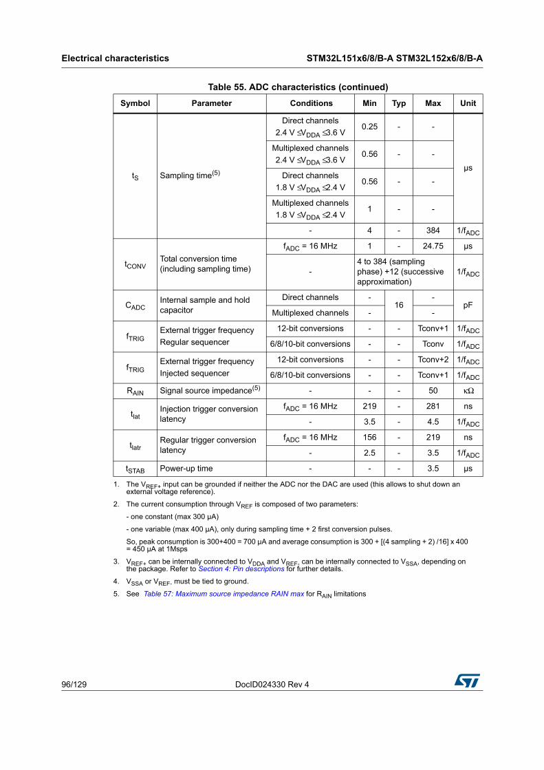
Electrical characteristics STM32L151x6/8/B-A STM32L152x6/8/B-A
96/129 DocID024330 Rev 4
tS Sampling time(5)
Direct channels
2.4 V ≤ VDDA ≤ 3.6 V0.25 - -
µs
Multiplexed channels
2.4 V ≤ VDDA ≤ 3.6 V0.56 - -
Direct channels
1.8 V ≤ VDDA ≤ 2.4 V0.56 - -
Multiplexed channels
1.8 V ≤ VDDA ≤ 2.4 V1 - -
- 4 - 384 1/fADC
tCONVTotal conversion time (including sampling time)
fADC = 16 MHz 1 - 24.75 µs
-4 to 384 (sampling phase) +12 (successive approximation)
1/fADC
CADCInternal sample and hold capacitor
Direct channels -16
-pF
Multiplexed channels - -
fTRIGExternal trigger frequency
Regular sequencer
12-bit conversions - - Tconv+1 1/fADC
6/8/10-bit conversions - - Tconv 1/fADC
fTRIGExternal trigger frequency
Injected sequencer
12-bit conversions - - Tconv+2 1/fADC
6/8/10-bit conversions - - Tconv+1 1/fADC
RAIN Signal source impedance(5) - - - 50 κΩ
tlatInjection trigger conversion latency
fADC = 16 MHz 219 - 281 ns
- 3.5 - 4.5 1/fADC
tlatrRegular trigger conversion latency
fADC = 16 MHz 156 - 219 ns
- 2.5 - 3.5 1/fADC
tSTAB Power-up time - - - 3.5 µs
1. The VREF+ input can be grounded if neither the ADC nor the DAC are used (this allows to shut down an external voltage reference).
2. The current consumption through VREF is composed of two parameters:
- one constant (max 300 µA)
- one variable (max 400 µA), only during sampling time + 2 first conversion pulses.
So, peak consumption is 300+400 = 700 µA and average consumption is 300 + [(4 sampling + 2) /16] x 400 = 450 µA at 1Msps
3. VREF+ can be internally connected to VDDA and VREF- can be internally connected to VSSA, depending on the package. Refer to Section 4: Pin descriptions for further details.
4. VSSA or VREF- must be tied to ground.
5. See Table 57: Maximum source impedance RAIN max for RAIN limitations
Table 55. ADC characteristics (continued)
Symbol Parameter Conditions Min Typ Max Unit
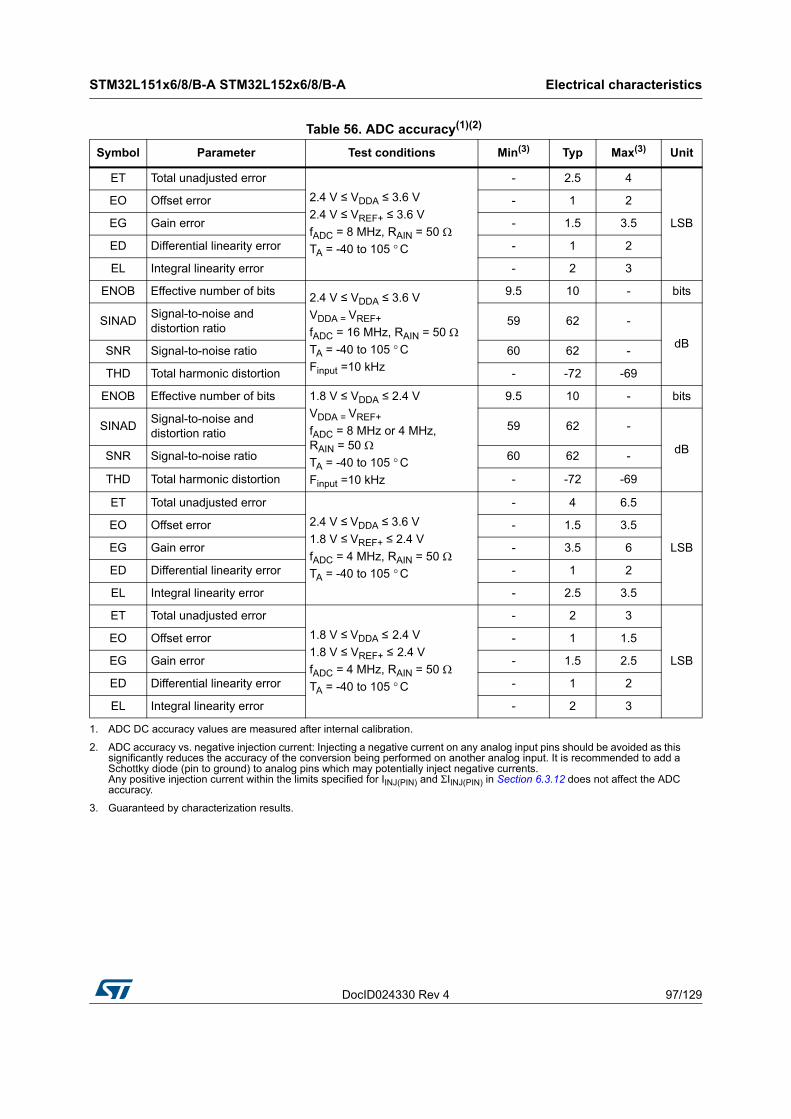
DocID024330 Rev 4 97/129
STM32L151x6/8/B-A STM32L152x6/8/B-A Electrical characteristics
105
Table 56. ADC accuracy(1)(2)
Symbol Parameter Test conditions Min(3) Typ Max(3) Unit
ET Total unadjusted error
2.4 V ≤ VDDA ≤ 3.6 V
2.4 V ≤ VREF+ ≤ 3.6 V
fADC = 8 MHz, RAIN = 50 ΩTA = -40 to 105 ° C
- 2.5 4
LSB
EO Offset error - 1 2
EG Gain error - 1.5 3.5
ED Differential linearity error - 1 2
EL Integral linearity error - 2 3
ENOB Effective number of bits2.4 V ≤ VDDA ≤ 3.6 V
VDDA = VREF+
fADC = 16 MHz, RAIN = 50 ΩTA = -40 to 105 ° C
Finput =10 kHz
9.5 10 - bits
SINADSignal-to-noise and distortion ratio
59 62 -
dBSNR Signal-to-noise ratio 60 62 -
THD Total harmonic distortion - -72 -69
ENOB Effective number of bits 1.8 V ≤ VDDA ≤ 2.4 V
VDDA = VREF+
fADC = 8 MHz or 4 MHz, RAIN = 50 ΩTA = -40 to 105 ° C
Finput =10 kHz
9.5 10 - bits
SINADSignal-to-noise and distortion ratio
59 62 -
dBSNR Signal-to-noise ratio 60 62 -
THD Total harmonic distortion - -72 -69
ET Total unadjusted error
2.4 V ≤ VDDA ≤ 3.6 V
1.8 V ≤ VREF+ ≤ 2.4 V
fADC = 4 MHz, RAIN = 50 ΩTA = -40 to 105 ° C
- 4 6.5
LSB
EO Offset error - 1.5 3.5
EG Gain error - 3.5 6
ED Differential linearity error - 1 2
EL Integral linearity error - 2.5 3.5
ET Total unadjusted error
1.8 V ≤ VDDA ≤ 2.4 V
1.8 V ≤ VREF+ ≤ 2.4 V
fADC = 4 MHz, RAIN = 50 ΩTA = -40 to 105 ° C
- 2 3
LSB
EO Offset error - 1 1.5
EG Gain error - 1.5 2.5
ED Differential linearity error - 1 2
EL Integral linearity error - 2 3
1. ADC DC accuracy values are measured after internal calibration.
2. ADC accuracy vs. negative injection current: Injecting a negative current on any analog input pins should be avoided as this significantly reduces the accuracy of the conversion being performed on another analog input. It is recommended to add a Schottky diode (pin to ground) to analog pins which may potentially inject negative currents. Any positive injection current within the limits specified for IINJ(PIN) and ΣIINJ(PIN) in Section 6.3.12 does not affect the ADC accuracy.
3. Guaranteed by characterization results.
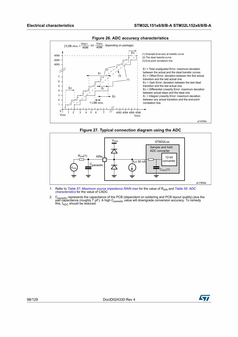
Electrical characteristics STM32L151x6/8/B-A STM32L152x6/8/B-A
98/129 DocID024330 Rev 4
Figure 26. ADC accuracy characteristics
Figure 27. Typical connection diagram using the ADC
1. Refer to Table 57: Maximum source impedance RAIN max for the value of RAIN and Table 55: ADC characteristics for the value of CADC
2. Cparasitic represents the capacitance of the PCB (dependent on soldering and PCB layout quality) plus the pad capacitance (roughly 7 pF). A high Cparasitic value will downgrade conversion accuracy. To remedy this, fADC should be reduced.
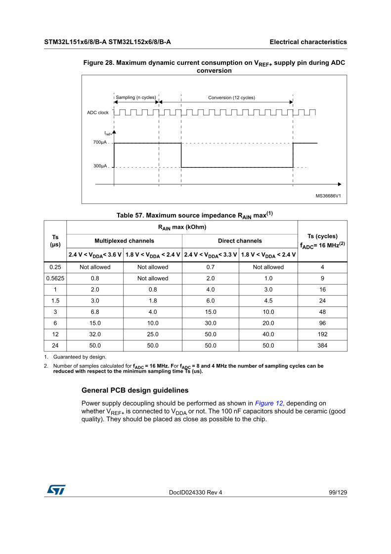
DocID024330 Rev 4 99/129
STM32L151x6/8/B-A STM32L152x6/8/B-A Electrical characteristics
105
Figure 28. Maximum dynamic current consumption on VREF+ supply pin during ADCconversion
General PCB design guidelines
Power supply decoupling should be performed as shown in Figure 12, depending on whether VREF+ is connected to VDDA or not. The 100 nF capacitors should be ceramic (good quality). They should be placed as close as possible to the chip.
ADC clock
Sampling (n cycles) Conversion (12 cycles)
Iref+
300µA
700µA
MS36686V1
Table 57. Maximum source impedance RAIN max(1)
Ts (µs)
RAIN max (kOhm)
Ts (cycles)
fADC= 16 MHz(2)Multiplexed channels Direct channels
2.4 V < VDDA< 3.6 V 1.8 V < VDDA < 2.4 V 2.4 V < VDDA< 3.3 V 1.8 V < VDDA < 2.4 V
0.25 Not allowed Not allowed 0.7 Not allowed 4
0.5625 0.8 Not allowed 2.0 1.0 9
1 2.0 0.8 4.0 3.0 16
1.5 3.0 1.8 6.0 4.5 24
3 6.8 4.0 15.0 10.0 48
6 15.0 10.0 30.0 20.0 96
12 32.0 25.0 50.0 40.0 192
24 50.0 50.0 50.0 50.0 384
1. Guaranteed by design.
2. Number of samples calculated for fADC = 16 MHz. For fADC = 8 and 4 MHz the number of sampling cycles can be reduced with respect to the minimum sampling time Ts (us).
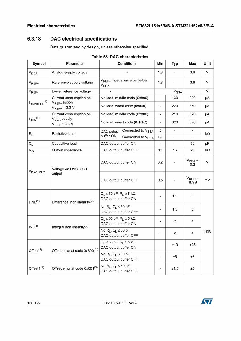
Electrical characteristics STM32L151x6/8/B-A STM32L152x6/8/B-A
100/129 DocID024330 Rev 4
6.3.18 DAC electrical specifications
Data guaranteed by design, unless otherwise specified.
Table 58. DAC characteristics
Symbol Parameter Conditions Min Typ Max Unit
VDDA Analog supply voltage - 1.8 - 3.6 V
VREF+ Reference supply voltageVREF+ must always be below VDDA
1.8 - 3.6 V
VREF- Lower reference voltage - VSSA V
IDDVREF+(1)
Current consumption on VREF+ supply
VREF+ = 3.3 V
No load, middle code (0x800) - 130 220 µA
No load, worst code (0x000) - 220 350 µA
IDDA(1)
Current consumption on VDDA supply
VDDA = 3.3 V
No load, middle code (0x800) - 210 320 µA
No load, worst code (0xF1C) - 320 520 µA
RL Resistive loadDAC output buffer ON
Connected to VSSA 5 - -kΩ
Connected to VDDA 25 - -
CL Capacitive load DAC output buffer ON - - 50 pF
RO Output impedance DAC output buffer OFF 12 16 20 kΩ
VDAC_OUT Voltage on DAC_OUT output
DAC output buffer ON 0.2 -VDDA –
0.2V
DAC output buffer OFF 0.5 -VREF+– 1LSB
mV
DNL(1) Differential non linearity(2)
CL ≤ 50 pF, RL ≥ 5 kΩDAC output buffer ON
- 1.5 3
LSB
No RL, CL ≤ 50 pF
DAC output buffer OFF- 1.5 3
INL(1) Integral non linearity(3)
CL ≤ 50 pF, RL ≥ 5 kΩDAC output buffer ON
- 2 4
No RL, CL ≤ 50 pF
DAC output buffer OFF- 2 4
Offset(1) Offset error at code 0x800 (4)
CL ≤ 50 pF, RL ≥ 5 kΩDAC output buffer ON
- ±10 ±25
No RL, CL ≤ 50 pF
DAC output buffer OFF- ±5 ±8
Offset1(1) Offset error at code 0x001(5) No RL, CL ≤ 50 pF
DAC output buffer OFF- ±1.5 ±5
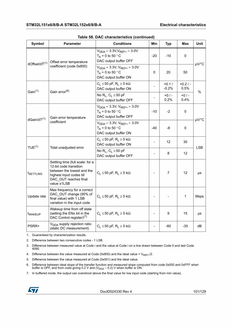
DocID024330 Rev 4 101/129
STM32L151x6/8/B-A STM32L152x6/8/B-A Electrical characteristics
105
dOffset/dT(1) Offset error temperature coefficient (code 0x800)
VDDA = 3.3V,VREF+ = 3.0V
TA = 0 to 50 ° C
DAC output buffer OFF
-20 -10 0
µV/°CVDDA = 3.3V, VREF+ = 3.0V
TA = 0 to 50 ° C
DAC output buffer ON
0 20 50
Gain(1) Gain error(6)
CL ≤ 50 pF, RL ≥ 5 kΩDAC output buffer ON
-+0.1 / -0.2%
+0.2 / -0.5%
%No RL, CL ≤ 50 pF
DAC output buffer OFF-
+0 / -0.2%
+0 / -0.4%
dGain/dT(1) Gain error temperature coefficient
VDDA = 3.3V, VREF+ = 3.0V
TA = 0 to 50 ° C
DAC output buffer OFF
-10 -2 0
µV/°CVDDA = 3.3V, VREF+ = 3.0V
TA = 0 to 50 ° C
DAC output buffer ON
-40 -8 0
TUE(1) Total unadjusted error
CL ≤ 50 pF, RL ≥ 5 kΩDAC output buffer ON
- 12 30
LSBNo RL, CL ≤ 50 pF
DAC output buffer OFF- 8 12
tSETTLING
Settling time (full scale: for a 12-bit code transition between the lowest and the highest input codes till DAC_OUT reaches final value ±1LSB
CL ≤ 50 pF, RL ≥ 5 kΩ - 7 12 µs
Update rate
Max frequency for a correct DAC_OUT change (95% of final value) with 1 LSB variation in the input code
CL ≤ 50 pF, RL ≥ 5 kΩ - - 1 Msps
tWAKEUP
Wakeup time from off state (setting the ENx bit in the DAC Control register)(7)
CL ≤ 50 pF, RL ≥ 5 kΩ - 9 15 µs
PSRR+VDDA supply rejection ratio (static DC measurement)
CL ≤ 50 pF, RL ≥ 5 kΩ - -60 -35 dB
1. Guaranteed by characterization results.
2. Difference between two consecutive codes - 1 LSB.
3. Difference between measured value at Code i and the value at Code i on a line drawn between Code 0 and last Code 4095.
4. Difference between the value measured at Code (0x800) and the ideal value = VREF+/2.
5. Difference between the value measured at Code (0x001) and the ideal value.
6. Difference between ideal slope of the transfer function and measured slope computed from code 0x000 and 0xFFF when buffer is OFF, and from code giving 0.2 V and (VDDA – 0.2) V when buffer is ON.
7. In buffered mode, the output can overshoot above the final value for low input code (starting from min value).
Table 58. DAC characteristics (continued)
Symbol Parameter Conditions Min Typ Max Unit
Electrical characteristics STM32L151x6/8/B-A STM32L152x6/8/B-A
102/129 DocID024330 Rev 4
Figure 29. 12-bit buffered /non-buffered DAC
1. The DAC integrates an output buffer that can be used to reduce the output impedance and to drive external loads directly without the use of an external operational amplifier. The buffer can be bypassed by configuring the BOFFx bit in the DAC_CR register.
6.3.19 Temperature sensor characteristics
Table 59. Temperature sensor calibration values
Calibration value name Description Memory address
TS_CAL1TS ADC raw data acquired at temperature of 30 °C±5, VDDA= 3 V ±10mV
0x1FF8 007A-0x1FF8 007B
TS_CAL2TS ADC raw data acquired at temperature of 110 ±5°C VDDA= 3 V ±10mV
0x1FF8 007E-0x1FF8 007F
Table 60. Temperature sensor characteristics
Symbol Parameter Min Typ Max Unit
TL(1)
1. Guaranteed by characterization results.
VSENSE linearity with temperature - ±1 ±2 °C
Avg_Slope(1) Average slope 1.48 1.61 1.75 mV/°C
V110 Voltage at 110°C ±5°C(2)
2. Measured at VDD = 3 V ±10 mV. V110 ADC conversion result is stored in the byte.
612 626.8 641.5 mV
IDDA(TEMP)(3) Current consumption - 3.4 6 µA
tSTART(3)
3. Guaranteed by design.
Startup time - - 10
µsTS_temp
(3) ADC sampling time when reading the temperature
4 - -
DocID024330 Rev 4 103/129
STM32L151x6/8/B-A STM32L152x6/8/B-A Electrical characteristics
105
6.3.20 Comparator
Table 61. Comparator 1 characteristics
Symbol Parameter Conditions Min(1) Typ Max(1)
1. Guaranteed by characterization results.
Unit
VDDA Analog supply voltage - 1.65 3.6 V
R400K R400K value - - 400 -kΩ
R10K R10K value - - 10 -
VINComparator 1 input voltage range
- 0.6 - VDDA V
tSTART Comparator startup time - - 7 10µs
td Propagation delay(2)
2. The delay is characterized for 100 mV input step with 10 mV overdrive on the inverting input, the non-inverting input set to the reference.
- - 3 10
Voffset Comparator offset - - ±3 ±10 mV
dVoffset/dtComparator offset variation in worst voltage stress conditions
VDDA = 3.6 V VIN+ = 0 V VIN- = VREFINT
TA = 25 ° C
0 1.5 10 mV/1000 h
ICOMP1 Current consumption(3)
3. Comparator consumption only. Internal reference voltage not included.
- - 160 260 nA
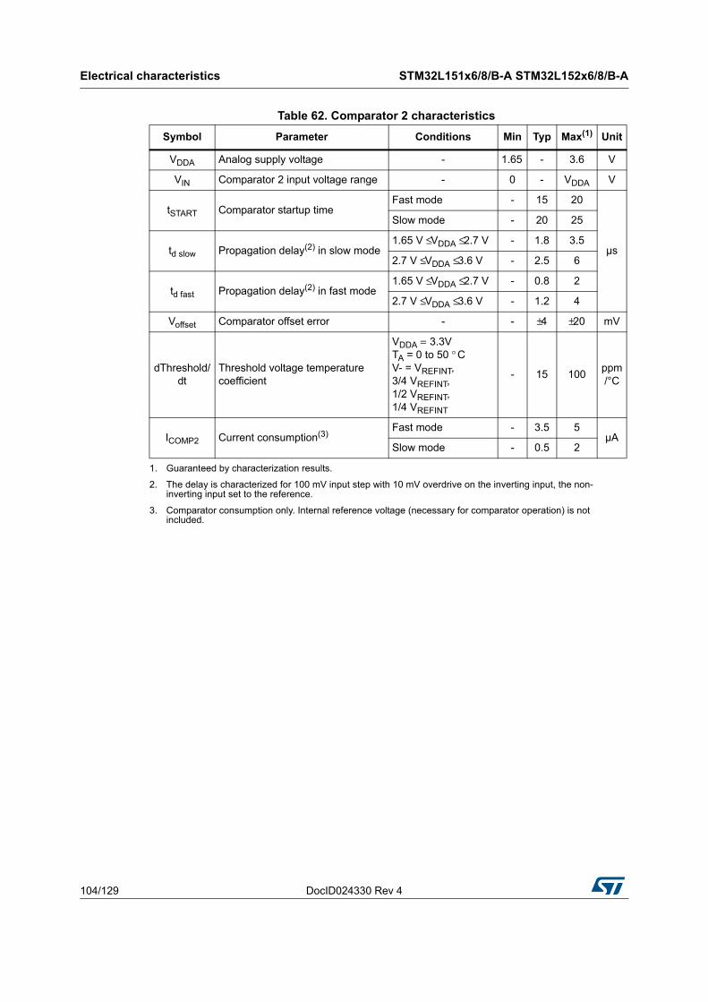
Electrical characteristics STM32L151x6/8/B-A STM32L152x6/8/B-A
104/129 DocID024330 Rev 4
Table 62. Comparator 2 characteristics
Symbol Parameter Conditions Min Typ Max(1)
1. Guaranteed by characterization results.
Unit
VDDA Analog supply voltage - 1.65 - 3.6 V
VIN Comparator 2 input voltage range - 0 - VDDA V
tSTART Comparator startup time Fast mode - 15 20
µs
Slow mode - 20 25
td slow Propagation delay(2) in slow mode
2. The delay is characterized for 100 mV input step with 10 mV overdrive on the inverting input, the non-inverting input set to the reference.
1.65 V ≤ VDDA ≤ 2.7 V - 1.8 3.5
2.7 V ≤ VDDA ≤ 3.6 V - 2.5 6
td fast Propagation delay(2) in fast mode1.65 V ≤ VDDA ≤ 2.7 V - 0.8 2
2.7 V ≤ VDDA ≤ 3.6 V - 1.2 4
Voffset Comparator offset error - - ±4 ±20 mV
dThreshold/dt
Threshold voltage temperature coefficient
VDDA = 3.3V TA = 0 to 50 ° C V- = VREFINT, 3/4 VREFINT, 1/2 VREFINT, 1/4 VREFINT
- 15 100ppm/°C
ICOMP2 Current consumption(3)
3. Comparator consumption only. Internal reference voltage (necessary for comparator operation) is not included.
Fast mode - 3.5 5µA
Slow mode - 0.5 2
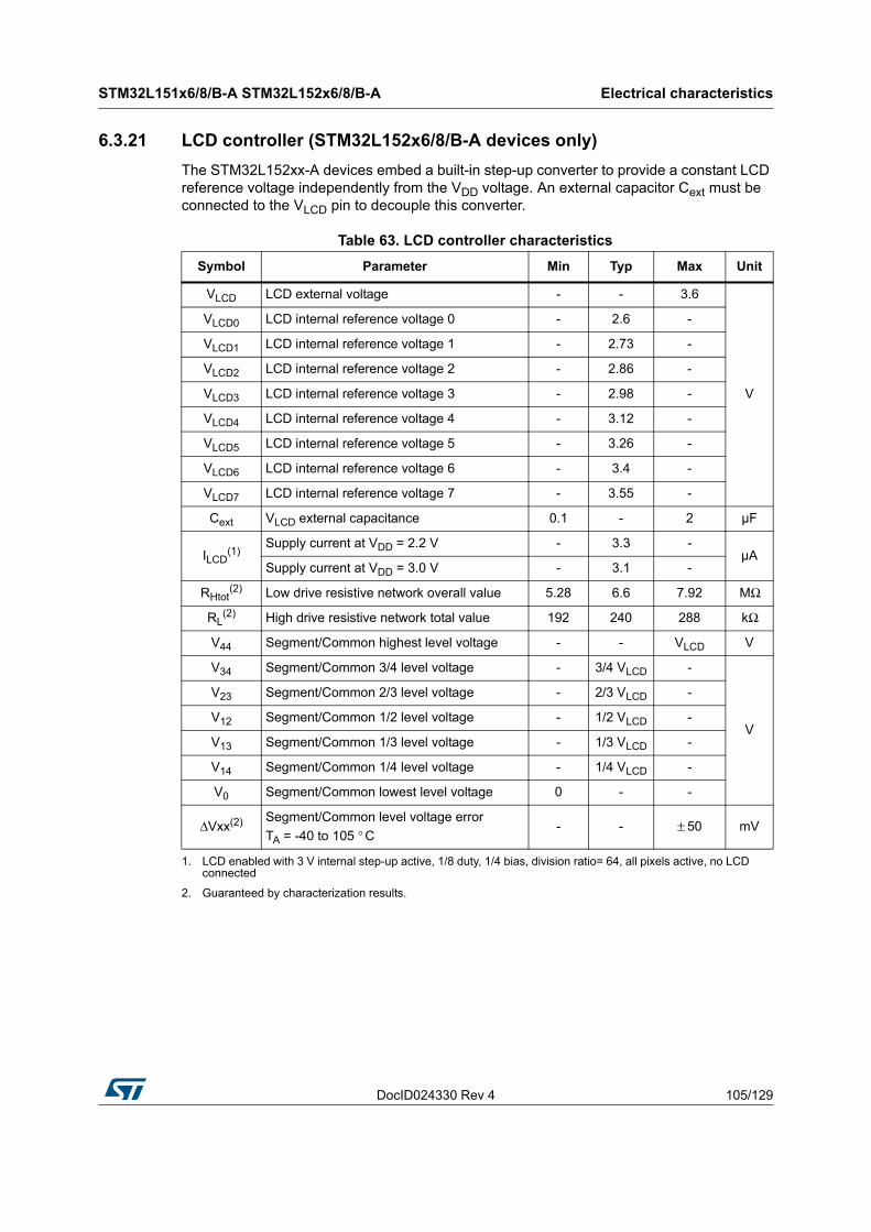
DocID024330 Rev 4 105/129
STM32L151x6/8/B-A STM32L152x6/8/B-A Electrical characteristics
105
6.3.21 LCD controller (STM32L152x6/8/B-A devices only)
The STM32L152xx-A devices embed a built-in step-up converter to provide a constant LCD reference voltage independently from the VDD voltage. An external capacitor Cext must be connected to the VLCD pin to decouple this converter.
Table 63. LCD controller characteristics
Symbol Parameter Min Typ Max Unit
VLCD LCD external voltage - - 3.6
V
VLCD0 LCD internal reference voltage 0 - 2.6 -
VLCD1 LCD internal reference voltage 1 - 2.73 -
VLCD2 LCD internal reference voltage 2 - 2.86 -
VLCD3 LCD internal reference voltage 3 - 2.98 -
VLCD4 LCD internal reference voltage 4 - 3.12 -
VLCD5 LCD internal reference voltage 5 - 3.26 -
VLCD6 LCD internal reference voltage 6 - 3.4 -
VLCD7 LCD internal reference voltage 7 - 3.55 -
Cext VLCD external capacitance 0.1 - 2 µF
ILCD(1)
1. LCD enabled with 3 V internal step-up active, 1/8 duty, 1/4 bias, division ratio= 64, all pixels active, no LCD connected
Supply current at VDD = 2.2 V - 3.3 -µA
Supply current at VDD = 3.0 V - 3.1 -
RHtot(2)
2. Guaranteed by characterization results.
Low drive resistive network overall value 5.28 6.6 7.92 MΩ
RL(2) High drive resistive network total value 192 240 288 kΩ
V44 Segment/Common highest level voltage - - VLCD V
V34 Segment/Common 3/4 level voltage - 3/4 VLCD -
V
V23 Segment/Common 2/3 level voltage - 2/3 VLCD -
V12 Segment/Common 1/2 level voltage - 1/2 VLCD -
V13 Segment/Common 1/3 level voltage - 1/3 VLCD -
V14 Segment/Common 1/4 level voltage - 1/4 VLCD -
V0 Segment/Common lowest level voltage 0 - -
ΔVxx(2) Segment/Common level voltage error
TA = -40 to 105 ° C- - ± 50 mV
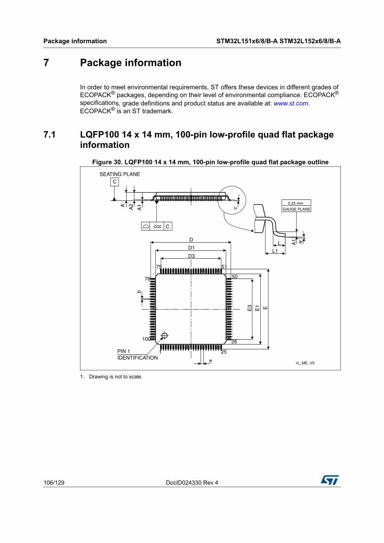
Package information STM32L151x6/8/B-A STM32L152x6/8/B-A
106/129 DocID024330 Rev 4
7 Package information
In order to meet environmental requirements, ST offers these devices in different grades of ECOPACK® packages, depending on their level of environmental compliance. ECOPACK® specifications, grade definitions and product status are available at: www.st.com. ECOPACK® is an ST trademark.
7.1 LQFP100 14 x 14 mm, 100-pin low-profile quad flat package information
Figure 30. LQFP100 14 x 14 mm, 100-pin low-profile quad flat package outline
1. Drawing is not to scale.
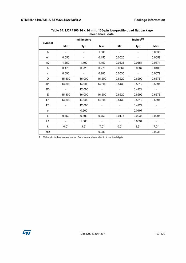
DocID024330 Rev 4 107/129
STM32L151x6/8/B-A STM32L152x6/8/B-A Package information
128
Table 64. LQPF100 14 x 14 mm, 100-pin low-profile quad flat package mechanical data
Symbolmillimeters inches(1)
1. Values in inches are converted from mm and rounded to 4 decimal digits.
Min Typ Max Min Typ Max
A - - 1.600 - - 0.0630
A1 0.050 - 0.150 0.0020 - 0.0059
A2 1.350 1.400 1.450 0.0531 0.0551 0.0571
b 0.170 0.220 0.270 0.0067 0.0087 0.0106
c 0.090 - 0.200 0.0035 - 0.0079
D 15.800 16.000 16.200 0.6220 0.6299 0.6378
D1 13.800 14.000 14.200 0.5433 0.5512 0.5591
D3 - 12.000 - - 0.4724 -
E 15.800 16.000 16.200 0.6220 0.6299 0.6378
E1 13.800 14.000 14.200 0.5433 0.5512 0.5591
E3 - 12.000 - - 0.4724 -
e - 0.500 - - 0.0197 -
L 0.450 0.600 0.750 0.0177 0.0236 0.0295
L1 - 1.000 - - 0.0394 -
k 0.0° 3.5° 7.0° 0.0° 3.5° 7.0°
ccc - - 0.080 - - 0.0031
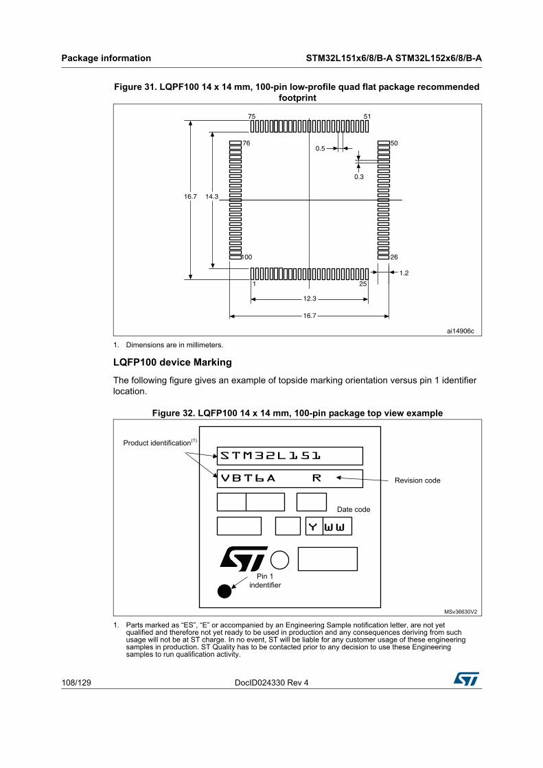
Package information STM32L151x6/8/B-A STM32L152x6/8/B-A
108/129 DocID024330 Rev 4
Figure 31. LQPF100 14 x 14 mm, 100-pin low-profile quad flat package recommended footprint
1. Dimensions are in millimeters.
LQFP100 device Marking
The following figure gives an example of topside marking orientation versus pin 1 identifier location.
Figure 32. LQFP100 14 x 14 mm, 100-pin package top view example
1. Parts marked as “ES”, “E” or accompanied by an Engineering Sample notification letter, are not yet qualified and therefore not yet ready to be used in production and any consequences deriving from such usage will not be at ST charge. In no event, ST will be liable for any customer usage of these engineering samples in production. ST Quality has to be contacted prior to any decision to use these Engineering samples to run qualification activity.
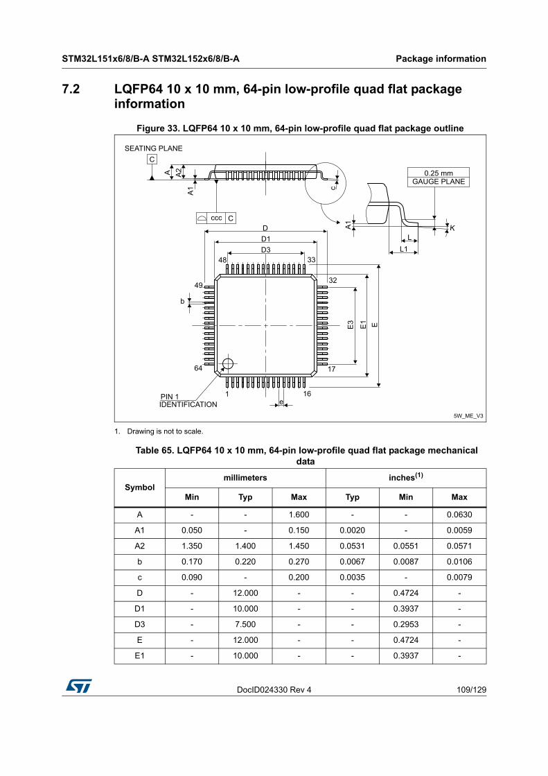
DocID024330 Rev 4 109/129
STM32L151x6/8/B-A STM32L152x6/8/B-A Package information
128
7.2 LQFP64 10 x 10 mm, 64-pin low-profile quad flat package information
Figure 33. LQFP64 10 x 10 mm, 64-pin low-profile quad flat package outline
1. Drawing is not to scale.
Table 65. LQFP64 10 x 10 mm, 64-pin low-profile quad flat package mechanical data
Symbolmillimeters inches(1)
Min Typ Max Typ Min Max
A - - 1.600 - - 0.0630
A1 0.050 - 0.150 0.0020 - 0.0059
A2 1.350 1.400 1.450 0.0531 0.0551 0.0571
b 0.170 0.220 0.270 0.0067 0.0087 0.0106
c 0.090 - 0.200 0.0035 - 0.0079
D - 12.000 - - 0.4724 -
D1 - 10.000 - - 0.3937 -
D3 - 7.500 - - 0.2953 -
E - 12.000 - - 0.4724 -
E1 - 10.000 - - 0.3937 -
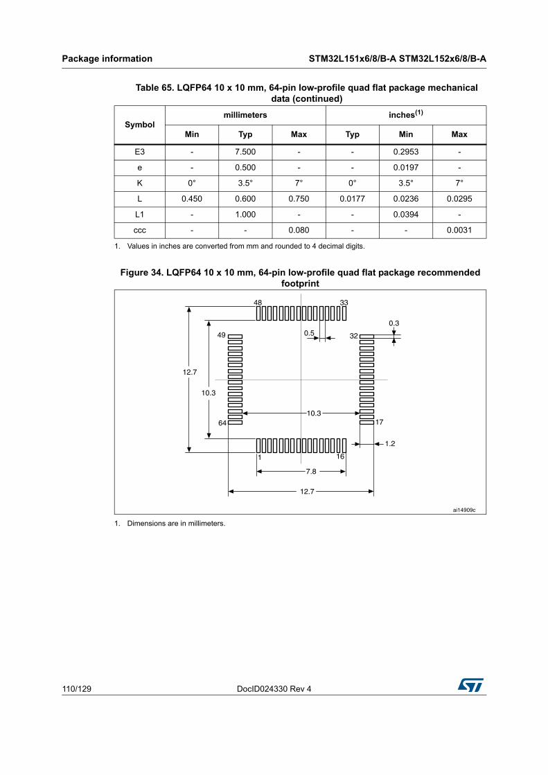
Package information STM32L151x6/8/B-A STM32L152x6/8/B-A
110/129 DocID024330 Rev 4
Figure 34. LQFP64 10 x 10 mm, 64-pin low-profile quad flat package recommended footprint
1. Dimensions are in millimeters.
E3 - 7.500 - - 0.2953 -
e - 0.500 - - 0.0197 -
K 0° 3.5° 7° 0° 3.5° 7°
L 0.450 0.600 0.750 0.0177 0.0236 0.0295
L1 - 1.000 - - 0.0394 -
ccc - - 0.080 - - 0.0031
1. Values in inches are converted from mm and rounded to 4 decimal digits.
Table 65. LQFP64 10 x 10 mm, 64-pin low-profile quad flat package mechanical data (continued)
Symbolmillimeters inches(1)
Min Typ Max Typ Min Max
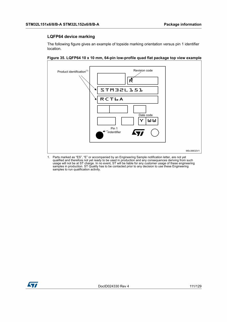
DocID024330 Rev 4 111/129
STM32L151x6/8/B-A STM32L152x6/8/B-A Package information
128
LQFP64 device marking
The following figure gives an example of topside marking orientation versus pin 1 identifier location.
Figure 35. LQFP64 10 x 10 mm, 64-pin low-profile quad flat package top view example
1. Parts marked as “ES”, “E” or accompanied by an Engineering Sample notification letter, are not yet qualified and therefore not yet ready to be used in production and any consequences deriving from such usage will not be at ST charge. In no event, ST will be liable for any customer usage of these engineering samples in production. ST Quality has to be contacted prior to any decision to use these Engineering samples to run qualification activity.
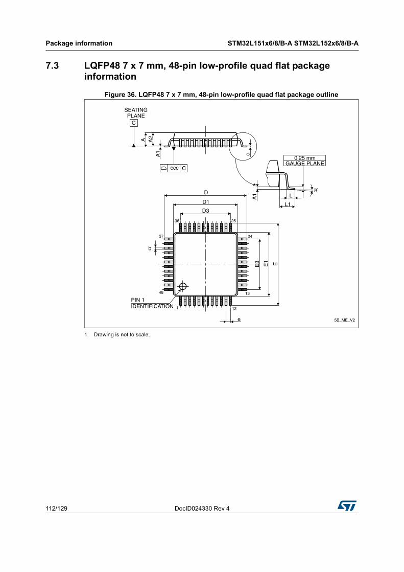
Package information STM32L151x6/8/B-A STM32L152x6/8/B-A
112/129 DocID024330 Rev 4
7.3 LQFP48 7 x 7 mm, 48-pin low-profile quad flat package information
Figure 36. LQFP48 7 x 7 mm, 48-pin low-profile quad flat package outline
1. Drawing is not to scale.
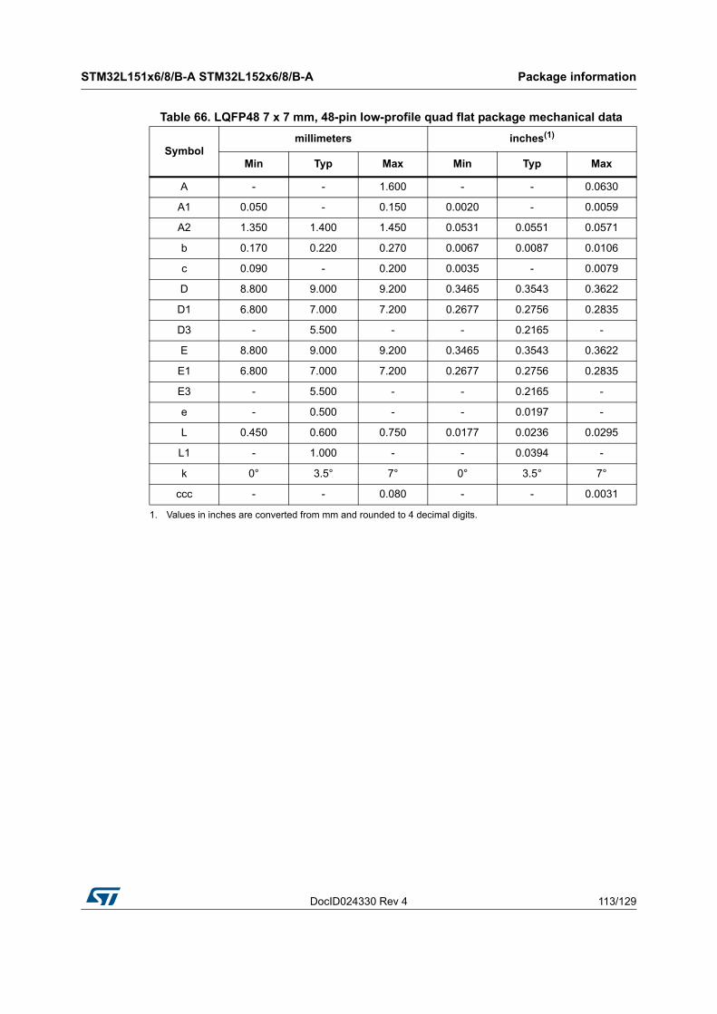
DocID024330 Rev 4 113/129
STM32L151x6/8/B-A STM32L152x6/8/B-A Package information
128
Table 66. LQFP48 7 x 7 mm, 48-pin low-profile quad flat package mechanical data
Symbolmillimeters inches(1)
1. Values in inches are converted from mm and rounded to 4 decimal digits.
Min Typ Max Min Typ Max
A - - 1.600 - - 0.0630
A1 0.050 - 0.150 0.0020 - 0.0059
A2 1.350 1.400 1.450 0.0531 0.0551 0.0571
b 0.170 0.220 0.270 0.0067 0.0087 0.0106
c 0.090 - 0.200 0.0035 - 0.0079
D 8.800 9.000 9.200 0.3465 0.3543 0.3622
D1 6.800 7.000 7.200 0.2677 0.2756 0.2835
D3 - 5.500 - - 0.2165 -
E 8.800 9.000 9.200 0.3465 0.3543 0.3622
E1 6.800 7.000 7.200 0.2677 0.2756 0.2835
E3 - 5.500 - - 0.2165 -
e - 0.500 - - 0.0197 -
L 0.450 0.600 0.750 0.0177 0.0236 0.0295
L1 - 1.000 - - 0.0394 -
k 0° 3.5° 7° 0° 3.5° 7°
ccc - - 0.080 - - 0.0031
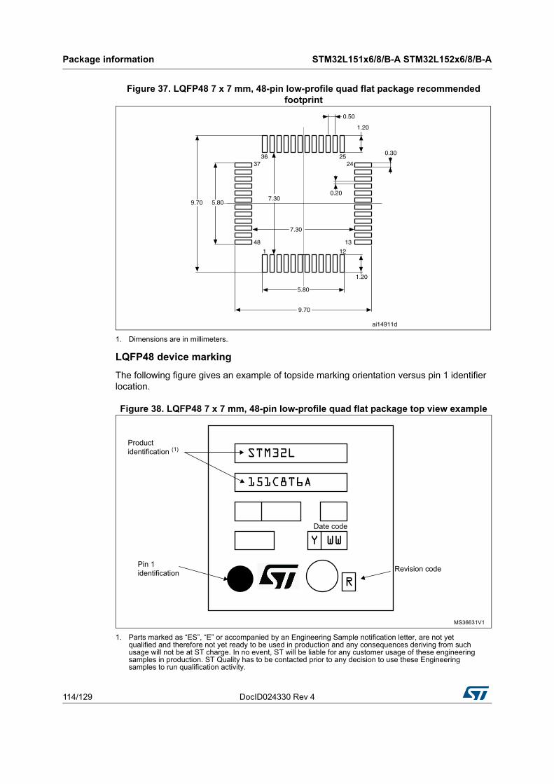
Package information STM32L151x6/8/B-A STM32L152x6/8/B-A
114/129 DocID024330 Rev 4
Figure 37. LQFP48 7 x 7 mm, 48-pin low-profile quad flat package recommended footprint
1. Dimensions are in millimeters.
LQFP48 device marking
The following figure gives an example of topside marking orientation versus pin 1 identifier location.
Figure 38. LQFP48 7 x 7 mm, 48-pin low-profile quad flat package top view example
1. Parts marked as “ES”, “E” or accompanied by an Engineering Sample notification letter, are not yet qualified and therefore not yet ready to be used in production and any consequences deriving from such usage will not be at ST charge. In no event, ST will be liable for any customer usage of these engineering samples in production. ST Quality has to be contacted prior to any decision to use these Engineering samples to run qualification activity.
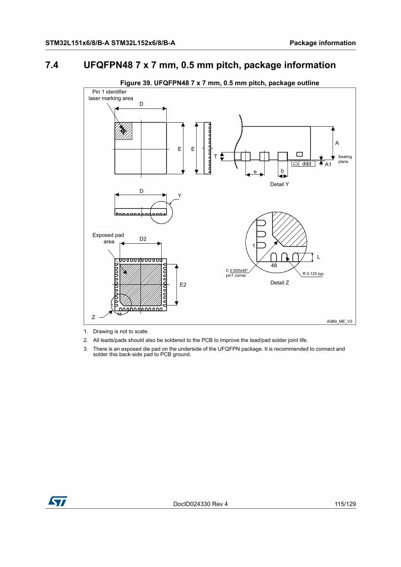
DocID024330 Rev 4 115/129
STM32L151x6/8/B-A STM32L152x6/8/B-A Package information
128
7.4 UFQFPN48 7 x 7 mm, 0.5 mm pitch, package information
Figure 39. UFQFPN48 7 x 7 mm, 0.5 mm pitch, package outline
1. Drawing is not to scale.
2. All leads/pads should also be soldered to the PCB to improve the lead/pad solder joint life.
3. There is an exposed die pad on the underside of the UFQFPN package. It is recommended to connect and solder this back-side pad to PCB ground.
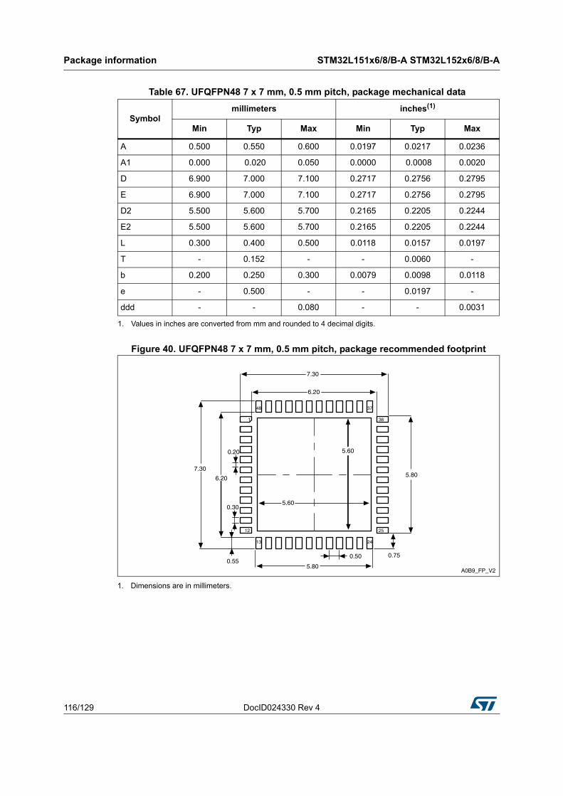
Package information STM32L151x6/8/B-A STM32L152x6/8/B-A
116/129 DocID024330 Rev 4
Figure 40. UFQFPN48 7 x 7 mm, 0.5 mm pitch, package recommended footprint
1. Dimensions are in millimeters.
Table 67. UFQFPN48 7 x 7 mm, 0.5 mm pitch, package mechanical data
Symbolmillimeters inches(1)
1. Values in inches are converted from mm and rounded to 4 decimal digits.
Min Typ Max Min Typ Max
A 0.500 0.550 0.600 0.0197 0.0217 0.0236
A1 0.000 0.020 0.050 0.0000 0.0008 0.0020
D 6.900 7.000 7.100 0.2717 0.2756 0.2795
E 6.900 7.000 7.100 0.2717 0.2756 0.2795
D2 5.500 5.600 5.700 0.2165 0.2205 0.2244
E2 5.500 5.600 5.700 0.2165 0.2205 0.2244
L 0.300 0.400 0.500 0.0118 0.0157 0.0197
T - 0.152 - - 0.0060 -
b 0.200 0.250 0.300 0.0079 0.0098 0.0118
e - 0.500 - - 0.0197 -
ddd - - 0.080 - - 0.0031
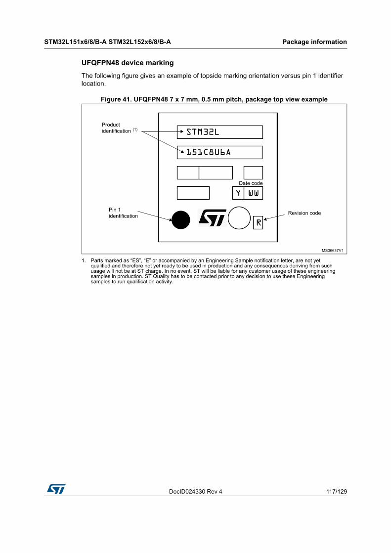
DocID024330 Rev 4 117/129
STM32L151x6/8/B-A STM32L152x6/8/B-A Package information
128
UFQFPN48 device marking
The following figure gives an example of topside marking orientation versus pin 1 identifier location.
Figure 41. UFQFPN48 7 x 7 mm, 0.5 mm pitch, package top view example
1. Parts marked as “ES”, “E” or accompanied by an Engineering Sample notification letter, are not yet qualified and therefore not yet ready to be used in production and any consequences deriving from such usage will not be at ST charge. In no event, ST will be liable for any customer usage of these engineering samples in production. ST Quality has to be contacted prior to any decision to use these Engineering samples to run qualification activity.
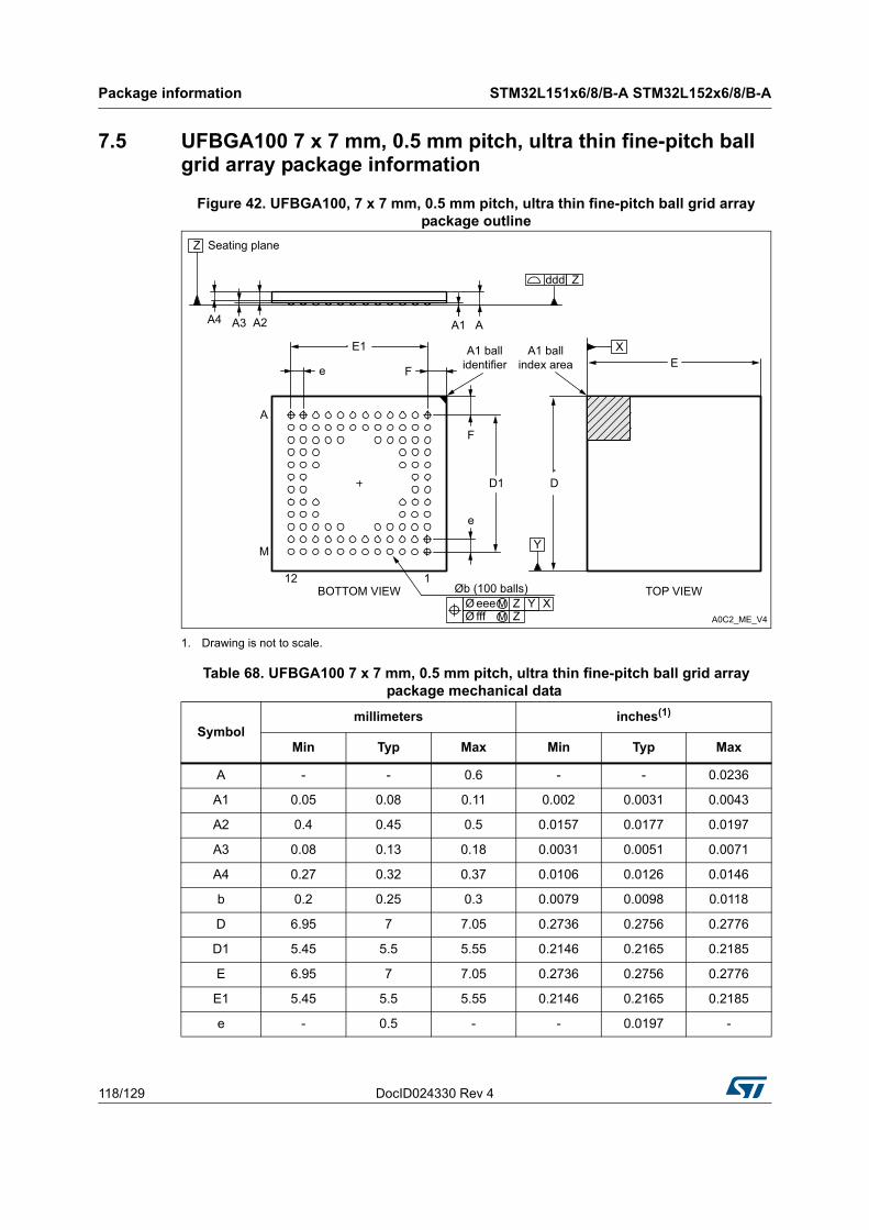
Package information STM32L151x6/8/B-A STM32L152x6/8/B-A
118/129 DocID024330 Rev 4
7.5 UFBGA100 7 x 7 mm, 0.5 mm pitch, ultra thin fine-pitch ball grid array package information
Figure 42. UFBGA100, 7 x 7 mm, 0.5 mm pitch, ultra thin fine-pitch ball grid arraypackage outline
1. Drawing is not to scale.
Table 68. UFBGA100 7 x 7 mm, 0.5 mm pitch, ultra thin fine-pitch ball grid arraypackage mechanical data
Symbolmillimeters inches(1)
Min Typ Max Min Typ Max
A - - 0.6 - - 0.0236
A1 0.05 0.08 0.11 0.002 0.0031 0.0043
A2 0.4 0.45 0.5 0.0157 0.0177 0.0197
A3 0.08 0.13 0.18 0.0031 0.0051 0.0071
A4 0.27 0.32 0.37 0.0106 0.0126 0.0146
b 0.2 0.25 0.3 0.0079 0.0098 0.0118
D 6.95 7 7.05 0.2736 0.2756 0.2776
D1 5.45 5.5 5.55 0.2146 0.2165 0.2185
E 6.95 7 7.05 0.2736 0.2756 0.2776
E1 5.45 5.5 5.55 0.2146 0.2165 0.2185
e - 0.5 - - 0.0197 -
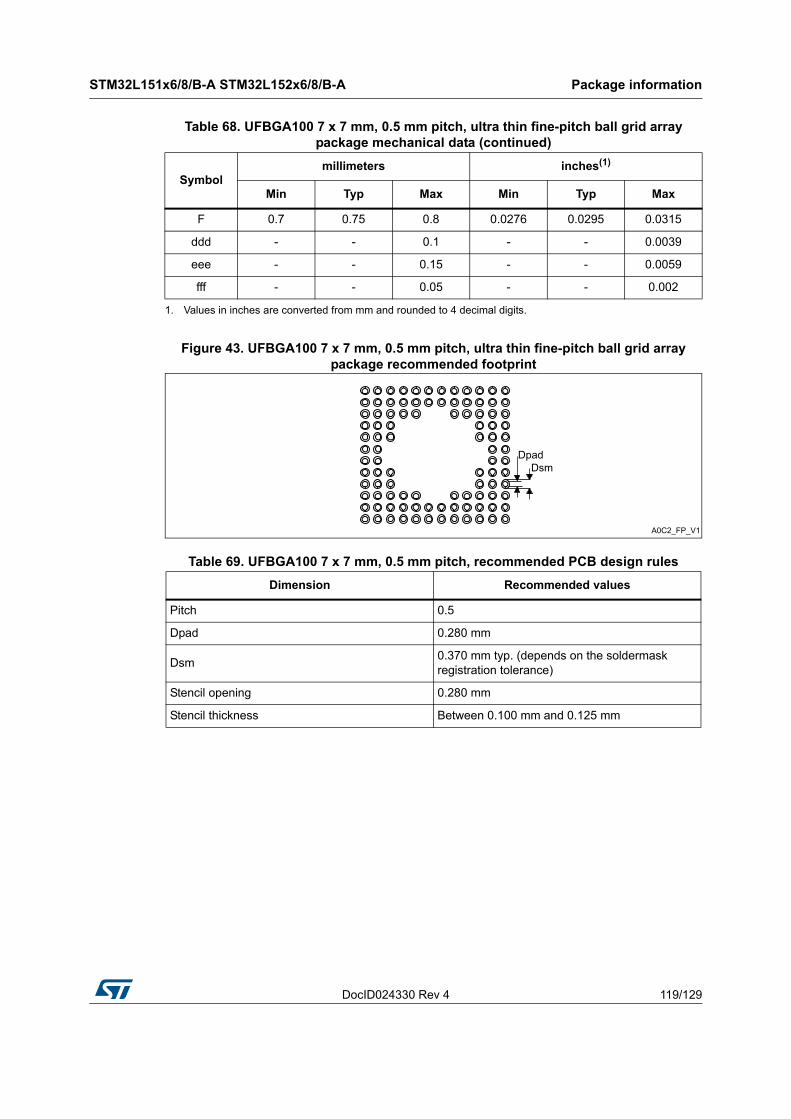
DocID024330 Rev 4 119/129
STM32L151x6/8/B-A STM32L152x6/8/B-A Package information
128
Figure 43. UFBGA100 7 x 7 mm, 0.5 mm pitch, ultra thin fine-pitch ball grid arraypackage recommended footprint
F 0.7 0.75 0.8 0.0276 0.0295 0.0315
ddd - - 0.1 - - 0.0039
eee - - 0.15 - - 0.0059
fff - - 0.05 - - 0.002
1. Values in inches are converted from mm and rounded to 4 decimal digits.
Table 69. UFBGA100 7 x 7 mm, 0.5 mm pitch, recommended PCB design rules
Dimension Recommended values
Pitch 0.5
Dpad 0.280 mm
Dsm0.370 mm typ. (depends on the soldermask registration tolerance)
Stencil opening 0.280 mm
Stencil thickness Between 0.100 mm and 0.125 mm
Table 68. UFBGA100 7 x 7 mm, 0.5 mm pitch, ultra thin fine-pitch ball grid arraypackage mechanical data (continued)
Symbolmillimeters inches(1)
Min Typ Max Min Typ Max
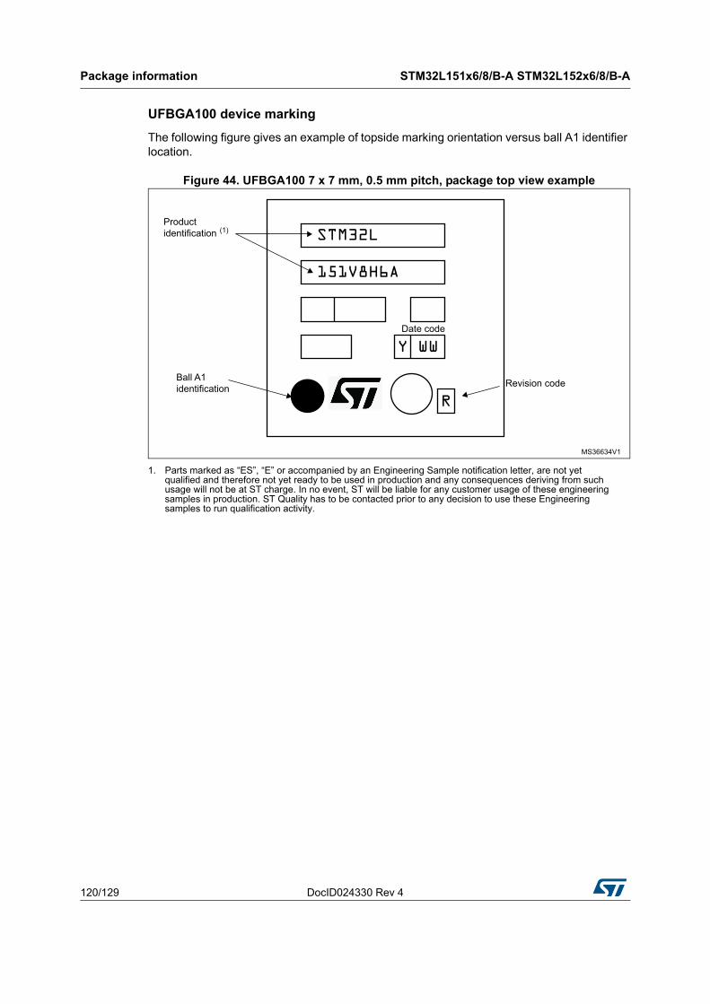
Package information STM32L151x6/8/B-A STM32L152x6/8/B-A
120/129 DocID024330 Rev 4
UFBGA100 device marking
The following figure gives an example of topside marking orientation versus ball A1 identifier location.
Figure 44. UFBGA100 7 x 7 mm, 0.5 mm pitch, package top view example
1. Parts marked as “ES”, “E” or accompanied by an Engineering Sample notification letter, are not yet qualified and therefore not yet ready to be used in production and any consequences deriving from such usage will not be at ST charge. In no event, ST will be liable for any customer usage of these engineering samples in production. ST Quality has to be contacted prior to any decision to use these Engineering samples to run qualification activity.
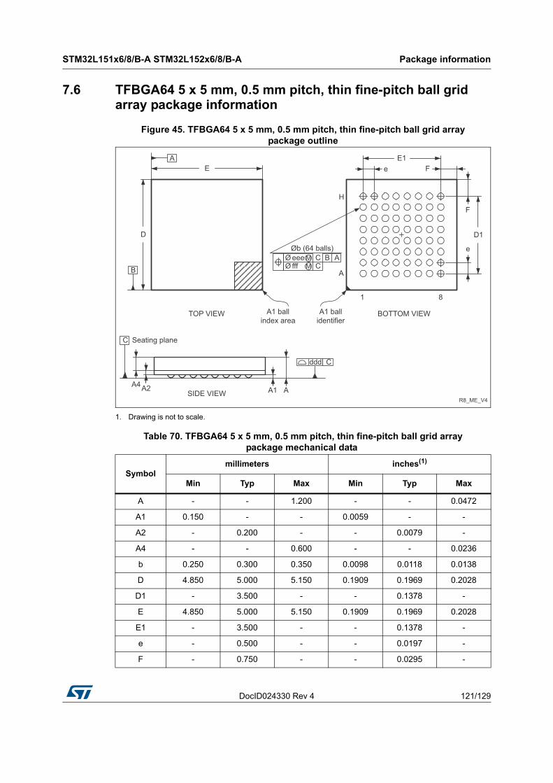
DocID024330 Rev 4 121/129
STM32L151x6/8/B-A STM32L152x6/8/B-A Package information
128
7.6 TFBGA64 5 x 5 mm, 0.5 mm pitch, thin fine-pitch ball grid array package information
Figure 45. TFBGA64 5 x 5 mm, 0.5 mm pitch, thin fine-pitch ball grid arraypackage outline
1. Drawing is not to scale.
Table 70. TFBGA64 5 x 5 mm, 0.5 mm pitch, thin fine-pitch ball grid arraypackage mechanical data
Symbolmillimeters inches(1)
Min Typ Max Min Typ Max
A - - 1.200 - - 0.0472
A1 0.150 - - 0.0059 - -
A2 - 0.200 - - 0.0079 -
A4 - - 0.600 - - 0.0236
b 0.250 0.300 0.350 0.0098 0.0118 0.0138
D 4.850 5.000 5.150 0.1909 0.1969 0.2028
D1 - 3.500 - - 0.1378 -
E 4.850 5.000 5.150 0.1909 0.1969 0.2028
E1 - 3.500 - - 0.1378 -
e - 0.500 - - 0.0197 -
F - 0.750 - - 0.0295 -
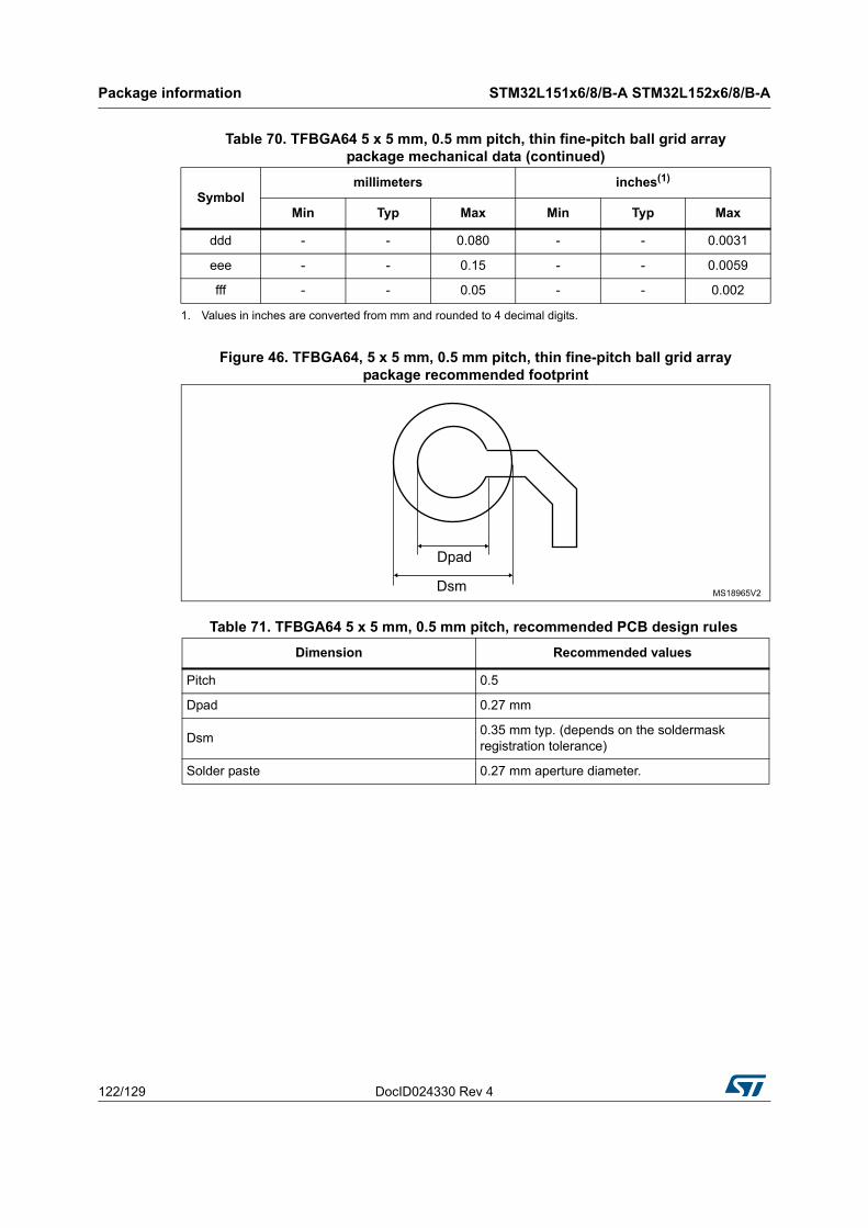
Package information STM32L151x6/8/B-A STM32L152x6/8/B-A
122/129 DocID024330 Rev 4
Figure 46. TFBGA64, 5 x 5 mm, 0.5 mm pitch, thin fine-pitch ball grid arraypackage recommended footprint
ddd - - 0.080 - - 0.0031
eee - - 0.15 - - 0.0059
fff - - 0.05 - - 0.002
1. Values in inches are converted from mm and rounded to 4 decimal digits.
Table 71. TFBGA64 5 x 5 mm, 0.5 mm pitch, recommended PCB design rules
Dimension Recommended values
Pitch 0.5
Dpad 0.27 mm
Dsm0.35 mm typ. (depends on the soldermask registration tolerance)
Solder paste 0.27 mm aperture diameter.
Table 70. TFBGA64 5 x 5 mm, 0.5 mm pitch, thin fine-pitch ball grid arraypackage mechanical data (continued)
Symbolmillimeters inches(1)
Min Typ Max Min Typ Max
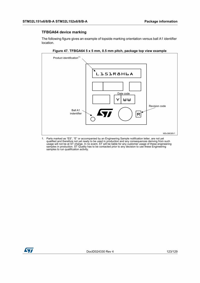
DocID024330 Rev 4 123/129
STM32L151x6/8/B-A STM32L152x6/8/B-A Package information
128
TFBGA64 device marking
The following figure gives an example of topside marking orientation versus ball A1 identifier location.
Figure 47. TFBGA64 5 x 5 mm, 0.5 mm pitch, package top view example
1. Parts marked as “ES”, “E” or accompanied by an Engineering Sample notification letter, are not yet qualified and therefore not yet ready to be used in production and any consequences deriving from such usage will not be at ST charge. In no event, ST will be liable for any customer usage of these engineering samples in production. ST Quality has to be contacted prior to any decision to use these Engineering samples to run qualification activity.
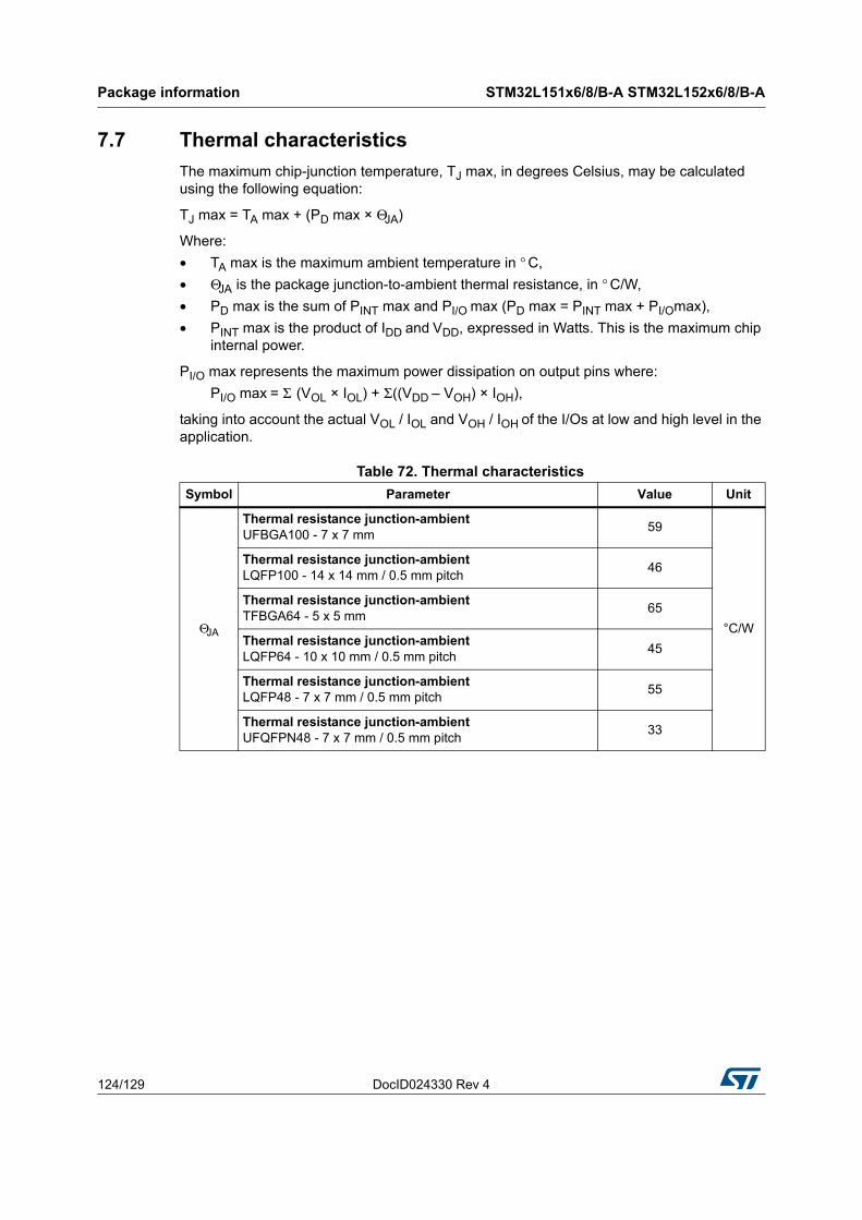
Package information STM32L151x6/8/B-A STM32L152x6/8/B-A
124/129 DocID024330 Rev 4
7.7 Thermal characteristics
The maximum chip-junction temperature, TJ max, in degrees Celsius, may be calculated using the following equation:
TJ max = TA max + (PD max × ΘJA)
Where:
• TA max is the maximum ambient temperature in ° C,
• ΘJA is the package junction-to-ambient thermal resistance, in ° C/W,
• PD max is the sum of PINT max and PI/O max (PD max = PINT max + PI/Omax),
• PINT max is the product of IDD and VDD, expressed in Watts. This is the maximum chip internal power.
PI/O max represents the maximum power dissipation on output pins where:
PI/O max = Σ (VOL × IOL) + Σ((VDD – VOH) × IOH),
taking into account the actual VOL / IOL and VOH / IOH of the I/Os at low and high level in the application.
Table 72. Thermal characteristics
Symbol Parameter Value Unit
ΘJA
Thermal resistance junction-ambient UFBGA100 - 7 x 7 mm
59
°C/W
Thermal resistance junction-ambient LQFP100 - 14 x 14 mm / 0.5 mm pitch
46
Thermal resistance junction-ambient TFBGA64 - 5 x 5 mm
65
Thermal resistance junction-ambient LQFP64 - 10 x 10 mm / 0.5 mm pitch
45
Thermal resistance junction-ambient LQFP48 - 7 x 7 mm / 0.5 mm pitch
55
Thermal resistance junction-ambient UFQFPN48 - 7 x 7 mm / 0.5 mm pitch
33
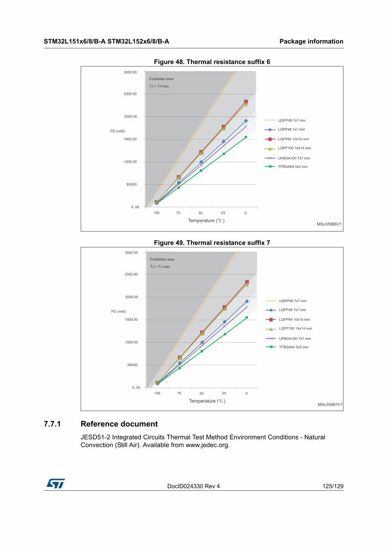
DocID024330 Rev 4 125/129
STM32L151x6/8/B-A STM32L152x6/8/B-A Package information
128
Figure 48. Thermal resistance suffix 6
Figure 49. Thermal resistance suffix 7
7.7.1 Reference document
JESD51-2 Integrated Circuits Thermal Test Method Environment Conditions - Natural Convection (Still Air). Available from www.jedec.org.
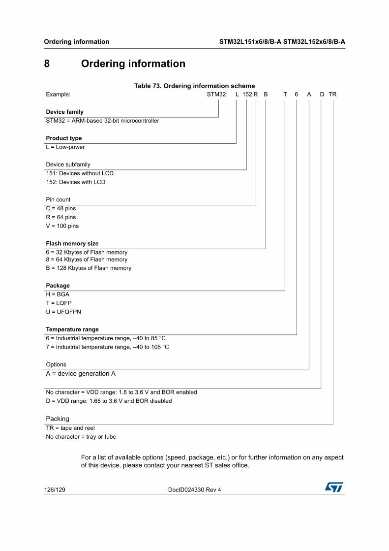
Ordering information STM32L151x6/8/B-A STM32L152x6/8/B-A
126/129 DocID024330 Rev 4
8 Ordering information
For a list of available options (speed, package, etc.) or for further information on any aspect of this device, please contact your nearest ST sales office.
Table 73. Ordering information schemeExample: STM32 L 152 R B T 6 A D TR
Device family
STM32 = ARM-based 32-bit microcontroller
Product type
L = Low-power
Device subfamily
151: Devices without LCD
152: Devices with LCD
Pin count
C = 48 pins
R = 64 pins
V = 100 pins
Flash memory size
6 = 32 Kbytes of Flash memory 8 = 64 Kbytes of Flash memory
B = 128 Kbytes of Flash memory
Package
H = BGA
T = LQFP
U = UFQFPN
Temperature range
6 = Industrial temperature range, –40 to 85 °C
7 = Industrial temperature range, –40 to 105 °C
Options
A = device generation A
No character = VDD range: 1.8 to 3.6 V and BOR enabled
D = VDD range: 1.65 to 3.6 V and BOR disabled
PackingTR = tape and reel
No character = tray or tube
DocID024330 Rev 4 127/129
STM32L151x6/8/B-A STM32L152x6/8/B-A Revision history
128
9 Revision history
Table 74. Document revision history
Date Revision Changes
04-Feb-2014 1 Initial release.
12-Mar-2014 2
Updated Section 3.5: Low-power real-time clock and backup registers, Section 6.1.2: Typical values and Section 6.3.4: Supply current characteristics.
Updated General PCB design guidelines.
Updated Table 5: Working mode-dependent functionalities (from Run/active down to standby), Table 14: General operating conditions, Table 21: Current consumption in Low-power run mode, Table 22: Current consumption in Low-power sleep mode, Table 23: Typical and maximum current consumptions in Stop mode, Table 24: Typical and maximum current consumptions in Standby mode, Table 25: Peripheral current consumption, Table 42: I/O current injection susceptibility, Table 66: I/O static characteristics and Table 46: NRST pin characteristics.
Updated Figure 14: Current consumption measurement scheme.
04-Feb-2015 3
Updated DMIPS features in cover page and Section 2: Description.
Updated max temperature at 105°C instead of 85°C in the whole datasheet.
Updated current consumption in Table 20: Current consumption in Sleep mode.
Updated Table 25: Peripheral current consumption with new measured values.
Updated Table 57: Maximum source impedance RAIN max adding note 2.
Updated Section 7: Package information with new package device marking.
Updated Figure 9: Memory map.
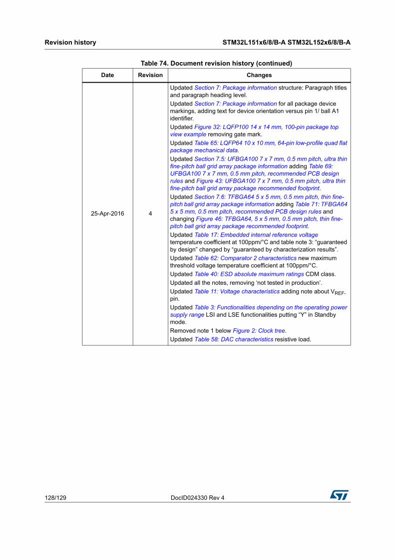
Revision history STM32L151x6/8/B-A STM32L152x6/8/B-A
128/129 DocID024330 Rev 4
25-Apr-2016 4
Updated Section 7: Package information structure: Paragraph titles and paragraph heading level.
Updated Section 7: Package information for all package device markings, adding text for device orientation versus pin 1/ ball A1 identifier.
Updated Figure 32: LQFP100 14 x 14 mm, 100-pin package top view example removing gate mark.
Updated Table 65: LQFP64 10 x 10 mm, 64-pin low-profile quad flat package mechanical data.
Updated Section 7.5: UFBGA100 7 x 7 mm, 0.5 mm pitch, ultra thin fine-pitch ball grid array package information adding Table 69: UFBGA100 7 x 7 mm, 0.5 mm pitch, recommended PCB design rules and Figure 43: UFBGA100 7 x 7 mm, 0.5 mm pitch, ultra thin fine-pitch ball grid array package recommended footprint.
Updated Section 7.6: TFBGA64 5 x 5 mm, 0.5 mm pitch, thin fine-pitch ball grid array package information adding Table 71: TFBGA64 5 x 5 mm, 0.5 mm pitch, recommended PCB design rules and changing Figure 46: TFBGA64, 5 x 5 mm, 0.5 mm pitch, thin fine-pitch ball grid array package recommended footprint.
Updated Table 17: Embedded internal reference voltage temperature coefficient at 100ppm/°C and table note 3: “guaranteed by design” changed by “guaranteed by characterization results”.
Updated Table 62: Comparator 2 characteristics new maximum threshold voltage temperature coefficient at 100ppm/°C.
Updated Table 40: ESD absolute maximum ratings CDM class.
Updated all the notes, removing ‘not tested in production’.
Updated Table 11: Voltage characteristics adding note about VREF- pin.
Updated Table 3: Functionalities depending on the operating power supply range LSI and LSE functionalities putting “Y” in Standby mode.
Removed note 1 below Figure 2: Clock tree.
Updated Table 58: DAC characteristics resistive load.
Table 74. Document revision history (continued)
Date Revision Changes
DocID024330 Rev 4 129/129
STM32L151x6/8/B-A STM32L152x6/8/B-A
129
IMPORTANT NOTICE – PLEASE READ CAREFULLY
STMicroelectronics NV and its subsidiaries (“ST”) reserve the right to make changes, corrections, enhancements, modifications, and improvements to ST products and/or to this document at any time without notice. Purchasers should obtain the latest relevant information on ST products before placing orders. ST products are sold pursuant to ST’s terms and conditions of sale in place at the time of order acknowledgement.
Purchasers are solely responsible for the choice, selection, and use of ST products and ST assumes no liability for application assistance or the design of Purchasers’ products.
No license, express or implied, to any intellectual property right is granted by ST herein.
Resale of ST products with provisions different from the information set forth herein shall void any warranty granted by ST for such product.
ST and the ST logo are trademarks of ST. All other product or service names are the property of their respective owners.
Information in this document supersedes and replaces information previously supplied in any prior versions of this document.
© 2016 STMicroelectronics – All rights reserved