Embed Size (px)
Citation preview

Product Specification
IXD5120
PS034301-0515 PRELIMINARY 1
Ultra Small, Low Power Consumption Voltage Detector
FEATURES
Accuracy ± 2% at VDF ≥ 1.5 V or ±0.03 V
Low Power Consumption at 0.6 μA typical at VDF = 2.7 V, VIN = 2.97 V
Detect Voltage Range 0.7 V – 5.0 V in 0.1 V increments
Operating Voltage Range 0.7 V – 6.0 V Detect Voltage Temperature Drift ±100 ppm/
0C
Output Configuration CMOS (Version C) or N-channel Open Drain (N Version)
Operating Ambient Temperature - 40 + 850C
Packages : USP-3 and SSOT-24
EU RoHS Compliant, Pb Free
APPLICATIONS
Microprocessor reset circuitry
Memory battery back-up circuits
Power-on reset circuits
Power failure detection
System battery life and charge voltage monitors
DESCRIPTION
The IXD5120 are highly precise, low power consumption, CMOS voltage detectors, manufactured using laser trimming technology.
With low power consumption and high accuracy, the series is suitable for precision mobile equipment.
The IXD5120 in ultra small packages are ideally suited for high-density PC boards.
The IXD5120 is available in both CMOS and N-channel open drain output configurations
Detector is available in USP-3 and SSOT-24 packages.
TYPICAL APPLICATION CIRCUIT TYPICAL PERFORMANCE CHARACTERISTIC
Pull-up Resistor RPL used with N-channel output configuaration only
Supply Current vs. Input Voltage IXD5120x272xx

Product Specification
IXD5120
PS033801-0515 PRELIMINARY 2
ABSOLUTE MAXIMUM RATINGS
PARAMETER SYMBOL RATINGS UNITS
Input Voltage VIN – 0.3 ~ +7.0 V
Output Current IOUT 10
mA
Output Voltage
CMOS Output VOUT – 0.3 ~ VIN + 0.3
V
N-channel Open Drain – 0.3 ~ +7.0 V
Power Dissipation2)
USP-3 PD
120 mW
SSOT-24 150
Operating Temperature Range TOPR – 40 ~ + 85 0C
Storage Temperature Range TSTG – 55 ~ +125 0C
All voltages are in respect to VSS
ELECTRICAL OPERATING CHARACTERISTICS
Ta = 25 0C
PARAMETER SYMBOL CONDITIONS MIN. TYP. MAX. UNIT CIRCUIT
Operating Voltage
VIN VDF(T) = 1.0 – 5.0 V1)
0.7 6.0 V
Detect Voltage
VDF
VDF(T) = 1.0 – 5.0 V E-12)
V
Hysteresis Width VHYS VDF(T) = 1.0 – 5.0 V VDF x 0.03
VDF x 0.05
VDF x 0.07
V
Supply Current1
ISS1 VIN = VDF(T) x 1.1 E -22 )
µA
Supply Current2
ISS2 VIN = VDF(T) x 0.9 E -32 )
µA
Output Current IOUTN
VIN = 0.7 V
VOUT = 0.5 V 0.09 0.57
mA
VOUT = 0.3 V 0.08 0.56
VOUT = 0.1 V 0.05 0.30
VIN = 1.0 V VOUT = 0.1 V, 1.0 V < VDF(T) ≤ 2.0 V 0.46 0.71
VIN = 2.0 V VOUT = 0.1 V, 2.0 V < VDF(T) ≤ 3.0 V 1.15 1.41
VIN = 3.0 V VOUT = 0.1 V, 3.0 V < VDF(T) ≤ 4.0 V 1.44 1.77
VIN = 4.0 V VOUT = 0.1 V, 4.0 V < VDF(T) 1,61 1.96
IOUTP3)
VIN = 6.0 V VOUT = 5.5 V -0.96 -0 . 60
Leakage Current ILEAK Version C VIN = VDF(T) x 0.9, VOUT = 0 V -0.001
µA Version N VIN = 6.0 V, VOUT = 6.0 V 0.001 0 .10
Detect Voltage Temperature
Characteristics
- 40 0C ≤ TOPR ≤ 85
0C ± 100 ppm/
0C
Detect Delay Time4)
tDF VIN = 6.0 V 0.7 V, from VIN = VDF to VOUT = 0.5 V 30 100 µs
Release Delay Time5)
tDR VIN = 0.7 V 6.0 V, from VIN = VDR to VOUT = VDR6) 20 100 µs
NOTE:
1) VDF(T) is a nominal detect voltage 2) Please refer to the table named Detect Voltage Accuracy and Supply Current Specifications 3) IXD5120C version only 4) Delay time from the moment, when VIN = VDF to the moment, when VOUT = 0.5 V, at VIN falling from 6.0 V to 0.7 V 5) Delay time from the moment, when VIN = VDR to the moment, when VOUT = VDR 6) Release voltage (VDR = VDF + VHYS)

Product Specification
IXD5120
PS034301-0515 PRELIMINARY 3
ELECTRICAL OPERATING CHARACTERISTICS (CONTINUED)
Detect Voltage Accuracy and Supply Current Specification
SYMBOL E-1 E-2 E-3
NOMINAL DETECT VOLTAGE
DETECT VOLTAGE VDF (V)
SUPPLY CURRENT1 ISS1 (μA)
SUPPLY CURRENT2 ISS2 (μA)
VDF(T) MIN. MAX. TYP. MAX. TYP. MAX.
1.0 0.970 1.030
0.5 1.4 0.4 1.35
1.1 1.070 1.130
1.2 1.170 1.230
1.3 1.270 1.330
1.4 1.370 1.430
1.5 1.470 1.530
1.6 1.568 1.632
1.7 1.666 1.734
1.8 1.764 1.836
1.9 1.862 1.938
2.0 1.960 2.040
0.6 1.7 0.5 1.60
2.1 2.058 2.142
2.2 2.156 2.244
2.3 2.254 2.346
2.4 2.352 2.448
2.5 2.450 2.550
2.6 2.548 2.652
2.7 2.646 2.754
2.8 2.744 2.856
0.7 1.9 0.6 1.80
2.9 2.842 2.958
3.0 2.940 3.060
3.1 3.038 3.162
3.2 3.136 3.264
3.3 3.234 3.366
3.4 3.332 3.468
3.5 3.430 3.570
3.6 3.528 3.672
3.7 3.626 3.774
3.8 3.724 3.876
3.9 3.822 3.978
4.0 3.920 4.080
4.1 4.018 4.182
4.2 4.116 4.284
4.3 4.214 4.386
4.4 4.312 4.488
4.5 4.410 4.590
4.6 4.508 4.692
4.7 4.606 4.794
4.8 4.704 4.896
4.9 4.802 4.998
5.0 4.900 5.100

Product Specification
IXD5120
PS033801-0515 PRELIMINARY 4
PIN CONFIGURATION
USP-3 SSOT-24
(BOTTOM VIEW) (TOP VIEW)
PIN ASSIGNMENT
PIN NUMBER PIN NAME FUNCTIONS
USP-3 SSOT-24
1 4 VIN Power Input
2 3 VOUT Output Voltage (Detect “LOW”)
3 2 VSS Ground
1 NC No Connection
BLOCK DIAGRAM
IXD5120C IXD5120N
Diodes inside the circuits are ESD protection diodes and parasitic diodes.
BASIC OPERATION
Operation of the IXD5120 in a typical application circuit is exlained by the timing diagram shown below.
Note: To simplfy explanation, an operation time of the circuit is not included.

Product Specification
IXD5120
PS034301-0515 PRELIMINARY 5
When input voltage VIN is higher than detect voltage VDF, output voltage VOUT is equal input voltage VIN. (Output of the IXD5120N version with N-channel open drain is in high impedance state.)
When input voltage VIN falls below detect voltage VDF, output voltage VOUT becomes equal to the ground voltage VSS level.
When input voltage VIN falls below minimum operating voltage VMIN, output becomes unstable. In this condition, VOUT is equal pull-up voltage, which is VIN in typical application.
When input voltage VIN rises above the minimum operating voltage VMIN, output keeps the ground voltage level VSS, until VIN becomes equal or higher than a release voltage VDR.
When the input voltage VIN rises above the release voltage VDR, output voltage VOUT becomes equal to the input voltage VIN. (Output of the IXD5120N version with N-channel open drain is in high impedance state.)
The difference between VDR and VDF represents the hysteresis width.
TYPICAL APPLICATION CIRCUIT
IXD5120C IXD5120N
LAYOUT AND USE CONSIDERATIONS
1. The IC may malfunction if absolute maximum ratings are exceeded. 2. To stabilize the IC's operations, please, ensure that VIN rise and fall times are more than several μs/V. 3. IXD5120N version with N-channel open drain configuration is recommended, when a resistive divider is
used to set VIN voltage (see figure below). Voltage drop at resistor RIN caused by supply and load currents, changes level of detect and release voltages. Those errors are not constant because of the fluctuation of currents. In addition, oscillation may occur if voltage drop caused by load or transient current exceeds hysteresis VHYS = VDR - VDF. In such cases, please ensure that RIN is less than 10 kΩ and that C is more than 0.1 μF.
IXD5120N Recommended Pull-up Resistors Value
INPUT VOLTAGE RANGE PULL-UP RESISTANCE
0.7V~6.0V ≥ 220kΩ
0.8V~6.0V ≥ 100kΩ
1.0V~6.0V ≥ 33kΩ

Product Specification
IXD5120
PS033801-0515 PRELIMINARY 6
TEST CIRCUITS
Circuit Circuit
Circuit Circuit
Pull-up Resistor RPL = 100 kΩ is used for IXD5120N version only
Product Specification
IXD5120
PS034301-0515 PRELIMINARY 7
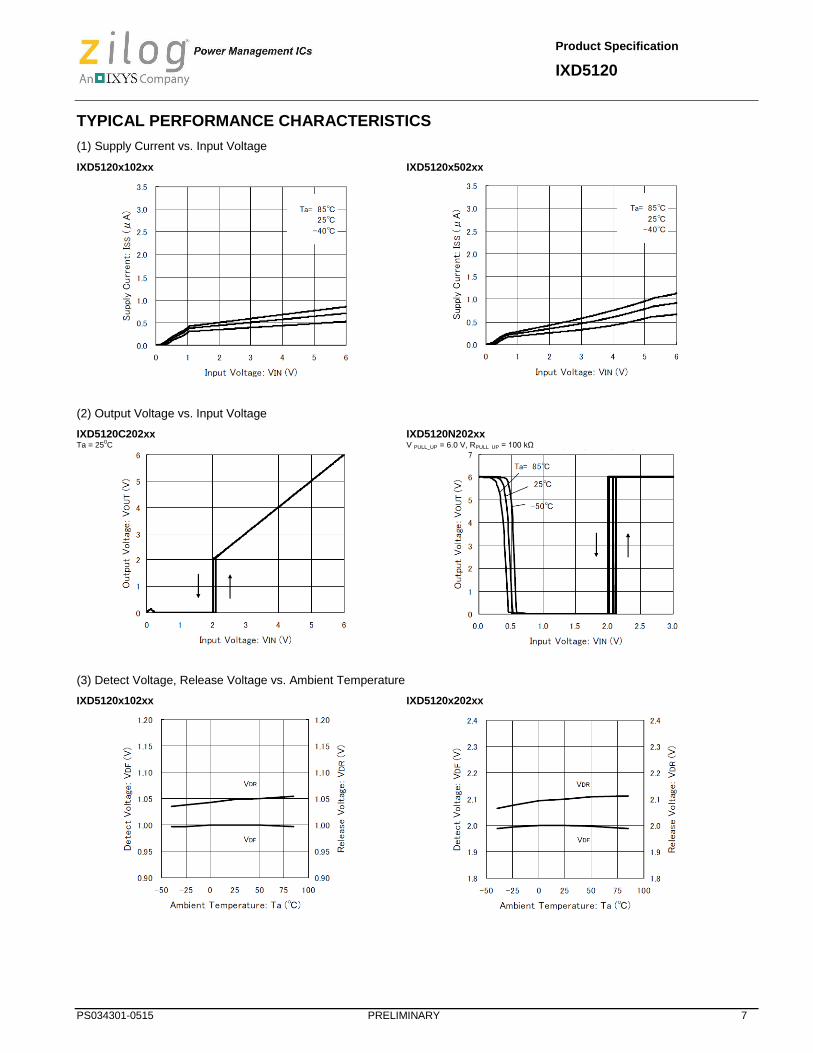
TYPICAL PERFORMANCE CHARACTERISTICS
(1) Supply Current vs. Input Voltage
IXD5120x102xx
IXD5120x502xx
(2) Output Voltage vs. Input Voltage
IXD5120C202xx Ta = 25
0C
IXD5120N202xx V PULL_UP = 6.0 V, RPULL_UP = 100 kΩ
(3) Detect Voltage, Release Voltage vs. Ambient Temperature
IXD5120x102xx
IXD5120x202xx
Product Specification
IXD5120
PS033801-0515 PRELIMINARY 8
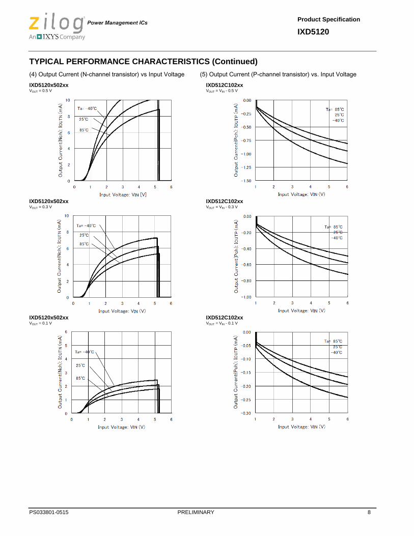
TYPICAL PERFORMANCE CHARACTERISTICS (Continued)
(4) Output Current (N-channel transistor) vs Input Voltage (5) Output Current (P-channel transistor) vs. Input Voltage
IXD5120x502xx VOUT = 0.5 V
IXD512C102xx VOUT = VIN - 0.5 V
IXD5120x502xx VOUT = 0.3 V
IXD512C102xx VOUT = VIN - 0.3 V
IXD5120x502xx VOUT = 0.1 V
IXD512C102xx VOUT = VIN - 0.1 V

Product Specification
IXD5120
PS034301-0515 PRELIMINARY 9
ORDERING INFORMATION
IXD5120-
DESIGNATOR DESCRIPTION SYMBOL DESCRIPTION
Output Configuration C CMOS output
N N-channel open drain output
Detect Voltage (VDF)
10 - 50 Detect Voltage Range: 1.0 V~5.0 V, e.g. 1.2 V - = 1, = 2
Detect Threshold Accuracy 2 ±2%
-(*)
Packages
(Order Unit)
HR USP-3 (3000/Reel)
HR-G USP-3 (1000/Reel)
NR SSOT-24 (3000/Reel)
NR-G SSOT-24 (3000/Reel)
NOTE:
The “-G” suffix denotes Halogen and Antimony free as well as being fully RoHS compliant.

Product Specification
IXD5120
PS033801-0515 PRELIMINARY 10
PACKAGE DRAWING AND DIMENSIONS
USP-3, Units: mm
SSOT-24, Units: mm
USP-3 Reference Pattern Layout, Units: mm
USP-3 Reference Metal Mask Design
Product Specification
IXD5120
PS034301-0515 PRELIMINARY 11
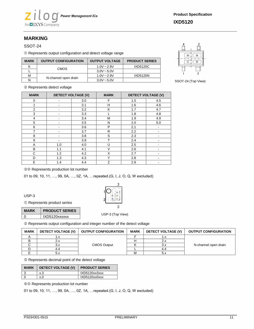
MARKING
SSOT-24
Represents output configuration and detect voltage range
MARK OUTPUT CONFIGURATION OUTPUT VOLTAGE PRODUCT SERIES
K CMOS
1.0V~2.9V IXD5120C
L 3.0V~5.0V
M N-channel open drain
1.0V~2.9V IXD5120N
N 3.0V~5.0V
Represents detect voltage
MARK DETECT VOLTAGE (V) MARK DETECT VOLTAGE (V)
0 - 3.0 F 1.5 4.5
1 - 3.1 H 1.6 4.6
2 - 3.2 K 1.7 4.7
3 - 3.3 L 1.8 4.8
4 - 3.4 M 1.9 4.9
5 - 3.5 N 2.0 5.0
6 - 3.6 P 2.1 -
7 - 3.7 R 2.2 -
8 - 3.8 S 2.3 -
9 - 3.9 T 2.4 -
A 1.0 4.0 U 2.5 -
B 1.1 4.1 V 2.6 -
C 1.2 4.2 X 2.7 -
D 1.3 4.3 Y 2.8 -
E 1.4 4.4 Z 2.9 -
Represents production lot number
01 to 09, 10, 11, …, 99, 0A, …, 0Z, 1A, …repeated.(G, I, J, O, Q, W excluded)
USP-3
Represents product series
MARK PRODUCT SERIES
0 IXD5120xxxxxx
Represents output configuration and integer number of the detect voltage
MARK DETECT VOLTAGE (V) OUTPUT CONFIGURATION MARK DETECT VOLTAGE (V) OUTPUT CONFIGURATION
A 1.x
CMOS Output
F 1.x
N-channel open drain
B 2.x H 2.x
C 3.x K 3.x
D 4.4 L 4.4
E 5.x M 5.x
Represents decimal point of the detect voltage
MARK DETECT VOLTAGE (V) PRODUCT SERIES
3 x.3 IXD5120xx3xxx
0 x.0 IXD5120xx0xxx
Represents production lot number
01 to 09, 10, 11, …, 99, 0A, …, 0Z, 1A, …repeated.(G, I, J, O, Q, W excluded)
USP-3 (Top View)
SSOT-24 (Top View)

Product Specification
IXD5120
PS033801-0515 PRELIMINARY 12
Customer Support
To share comments, get your technical questions answered, or report issues you may be experiencing with our products, please visit Zilog’s Technical Support page at http://support.zilog.com. To learn more about this product, find additional documentation, or to discover other fac-ets about Zilog product offerings, please visit the Zilog Knowledge Base at http:// zilog.com/kb or consider participating in the Zilog Forum at http://zilog.com/forum. This publication is subject to replacement by a later edition. To determine whether a later edition exists, please visit the Zilog website at http://www.zilog.com.
Warning: DO NOT USE THIS PRODUCT IN LIFE SUPPORT SYSTEMS.
LIFE SUPPORT POLICY ZILOG’S PRODUCTS ARE NOT AUTHORIZED FOR USE AS CRITICAL COMPONENTS IN LIFE SUPPORT DEVICES OR SYSTEMS WITHOUT THE EXPRESS PRIOR WRITTEN APPROVAL OF THE PRESIDENT AND GENERAL COUNSEL OF ZILOG CORPORATION.
As used herein Life support devices or systems are devices which (a) are intended for surgical implant into the body, or (b) support or sustain life and whose failure to perform when properly used in accordance with instructions for use provided in the labeling can be reasonably expected to result in a significant injury to the user. A critical component is any component in a life support device or system whose failure to perform can be reasonably expected to cause the failure of the life support device or system or to affect its safety or effectiveness.
Document Disclaimer ©2015 Zilog, Inc. All rights reserved. Information in this publication concerning the devices, applications, or technology described is intended to suggest possible uses and may be superseded. ZILOG, INC. DOES NOT ASSUME LIABILITY FOR OR PROVIDE A REPRESENTATION OF ACCURACY OF THE INFORMATION, DEVICES, OR TECHNOLOGY DESCRIBED IN THIS DOCUMENT. ZILOG ALSO DOES NOT ASSUME LIABILITY FOR INTELLECTUAL PROPERTY INFRINGEMENT RELATED IN ANY MANNER TO USE OF INFORMATION, DEVICES, OR TECHNOLOGY DESCRIBED HEREIN OR OTHERWISE. The information contained within this document has been verified according to the general principles of electrical and mechanical engineering.