Embed Size (px)
Citation preview
SUPPLEMENTARY INFORMATIONDOI: 10.1038/NNANO.2011.123
NATURE NANOTECHNOLOGY | www.nature.com/naturenanotechnology 1
1
Ultra-strong Adhesion of Graphene Membranes
Steven P. Koenig, Narasimha G. Boddeti, Martin L. Dunn, and J. Scott Bunch*
Department of Mechanical Engineering, University of Colorado, Boulder, CO 80309 USA
*email: [email protected]
Supplementary Information:
Counting Number of Graphene Layers
In order to count the number of graphene layers used in this study we employed a
combination of optical contrast, Raman spectroscopy, AFM measurements, and the elastic
constant measurements. Raman spectroscopy has been demonstrated to be a powerful tool
for identifying single layer graphene sheets 1. Recently Raman has also been shown to be
able to identify the number of layers of few layer graphene, a technique we use here2.
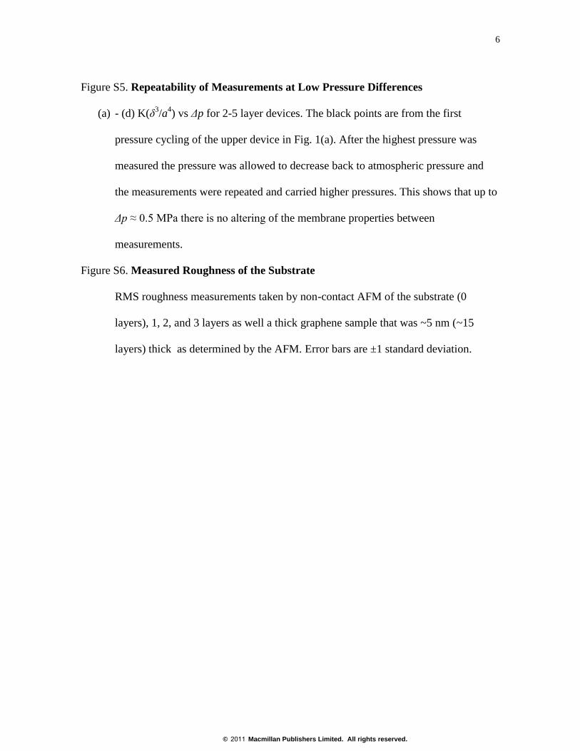
Figure S1 (a) and (b) show the graphene flakes from this study and the spots where Raman
spectrum was taken for each device, black is 1 layer, red is 2 layers, green is 3 layers, blue
is 4 layers and cyan is 5 layers. Figure S1 (c) and (d) show the Raman spectrum taken from
the spots of corresponding color in (a) and (b) respectively. To verify the number of layers
we found the ratio of the integrated intensity of the first order optical phonon peak and the
graphene G peak. The ratios are shown in figure S1 (e) and (f). Comparing these values
with the Fresnel equation we can determine the number of layers for each region. In order
to verify this technique we used optical contrast, AFM measurements, as well as the elastic
constants of the membranes 3. The optical contrast and AFM measurements showed close
agreement to the Raman spectroscopy technique validating its utility.
© 2011 Macmillan Publishers Limited. All rights reserved.
2
Adhesion Energy and Elastic Constants Measurements
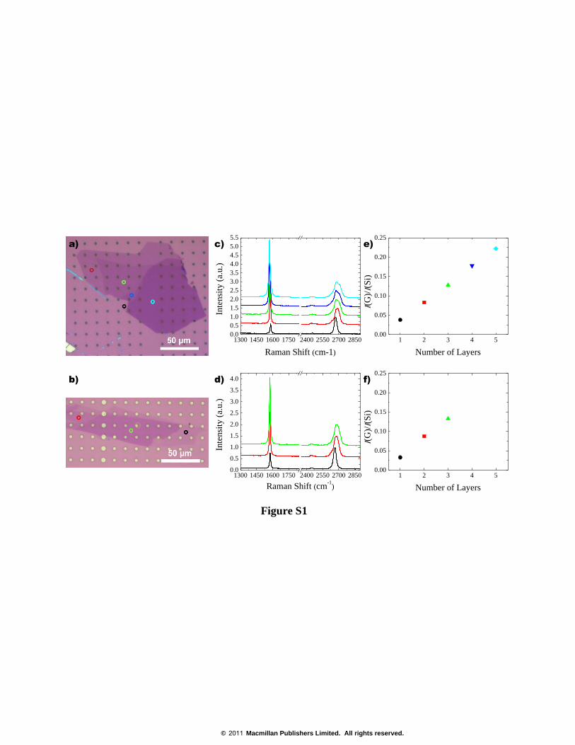
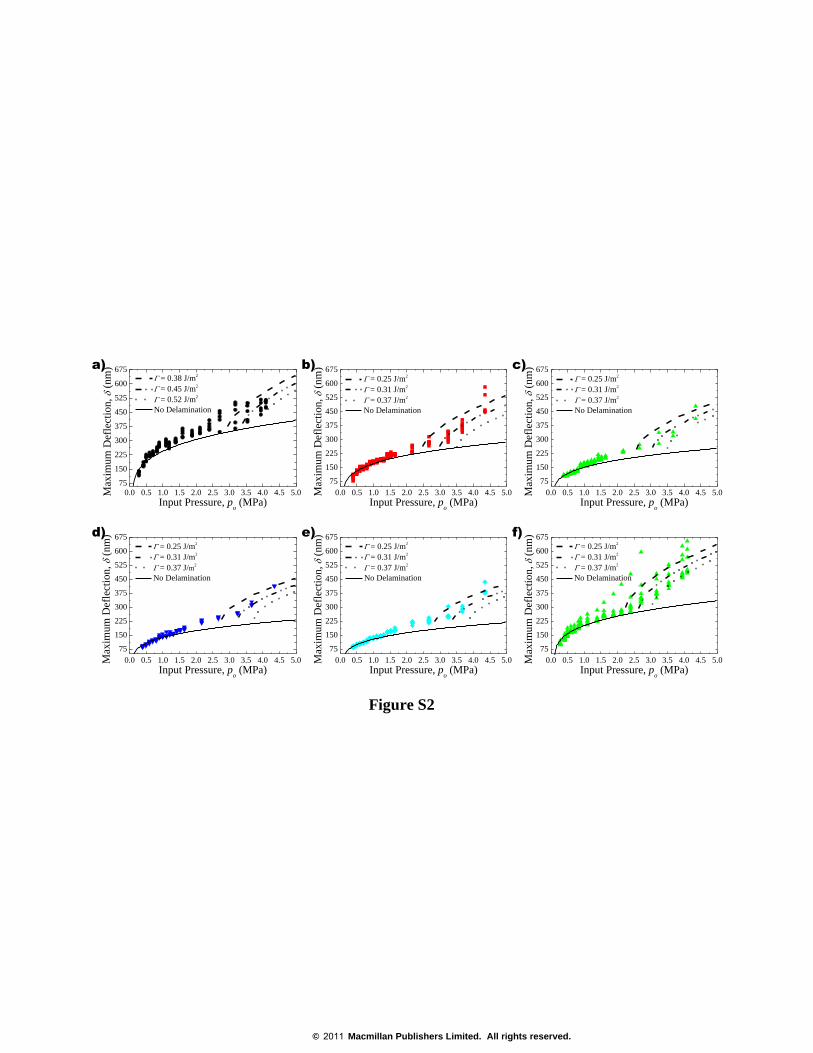
The adhesion energy measurements were carried out according to the main text of
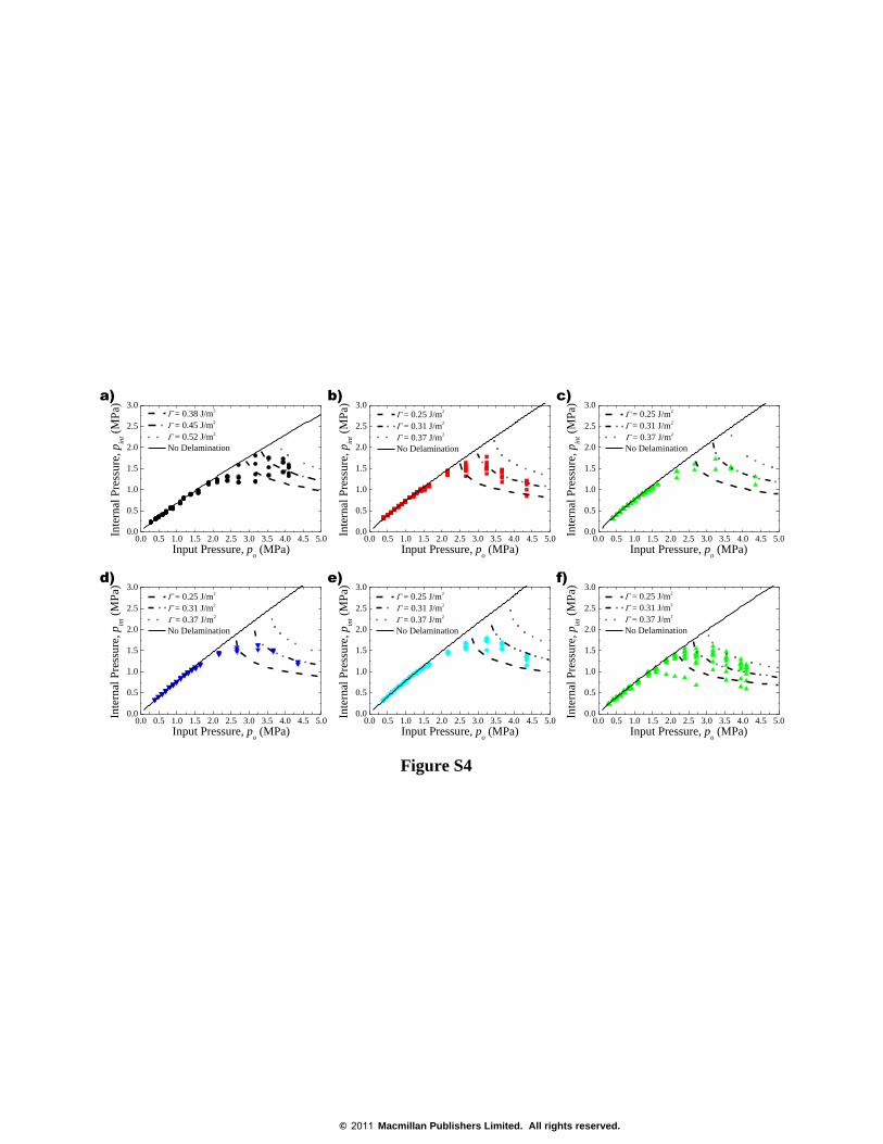
this article. Figures S2, S3, and S4 show (a) δ vs. p0, (b) a vs. p0, and (c) pint vs. p0, for all
the membranes studied. The layer numbers are as follows: (a) 1 layer membranes from Fig.
1 (lower). (b) 2 layer membranes from Fig. 1 (upper). (c) 3 layer membranes from Fig. 1
(upper). 4 layer membranes from Fig. 1 (upper). (d) 5 layer membranes from Fig. 1 (upper).
and (e) 3 layer membranes from Fig. 1 (lower).
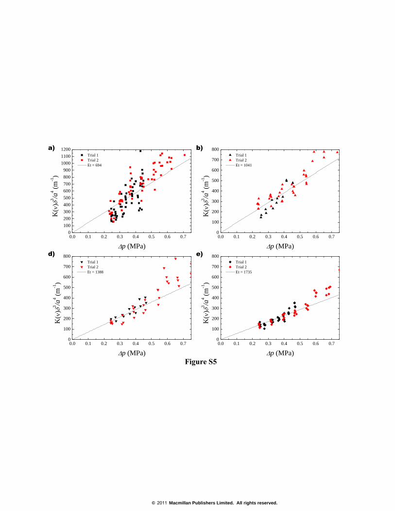
Repeatability of Elastic Constant Measurements
To verify the repeatability of the measurement of the elastic constants at Δp < 0.5
MPa we first pressurized the graphene flake in Fig. 1a(upper) up to Δp = 0.45 MPa and
then let pressure decrease back to Δp = 0 MPa. We then repeated the measurements and
increased Δp until there was significant peeling from the substrate in order to test the
adhesion strength. Figure S5 shows the results from this test for (a) 2 layers, (b) 3 layers,
(c) 4 layers, and (d) 5 layers of graphene. From this we conclude that pressurizing the
membranes does not cause sliding or change the membrane properties when Δp < 0.5 MPa
and therefore the membrane can be considered to be well clamped to the substrate in this
pressure range.
Adhesion from Trapped Charges in SiO2
We use the method of image charges to estimate the influence of trapped charges in the
SiO2 on the adhesion of graphene to the substrate. The work needed to move a charge from
a distance d from the conducting plane out to infinity is:
© 2011 Macmillan Publishers Limited. All rights reserved.
3
where q is the fundamental charge, d is the distance the charge is away from the conducting
plane and is the permittivity of free space4. In order to determine an adhesion energy we
also need to know the area density of charges, ρ, and the equation becomes:
If we assume all the charges are on the surface of the SiO2 and that the equilibrium spacing
between the graphene and SiO2 is equal to that of the equilibrium spacing of graphite d =
0.34 nm. The charge density needed to produce our measured adhesion energy of 0.31 J/m2
is ~9x10¹⁷
m-2
. The charge density of SiO2 is reported to be 2.3x10¹⁵
m-2
5. Seeing that the
reported value of the charge density in SiO2 is almost three orders of magnitude lower, we
can conclude that trapped charges do not have a significant contribution to the adhesion
energy value we measure. Other studies have used potassium ions to increase the charge
density present in the oxide 6. The concentration of potassium ions was as high as ~5 x 10
16
m2. This upper limit of the extrinsic doping concentration results in a charge density that is
one order of magnitude less than that needed to have adhesion energies on the order of what
we measured. These results show that the effect of charge impurities in the SiO2 below the
graphene will not significantly influence our measure of adhesion energy.
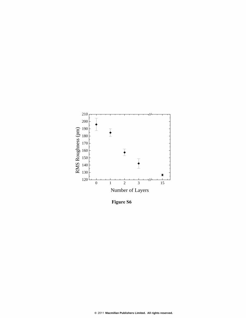
RMS Roughness and Conformation
Roughness measurements were taken using a Veeco Dimension 3100 operating
under non-contact mode under ambient conditions. The bare SiO2 substrate is denoted as 0
layers in Fig. S6 and a ~5nm thick flake as measured by the AFM was estimated to be
© 2011 Macmillan Publishers Limited. All rights reserved.
4
approximately 15 layers thick. For the roughness measurements of the substrate and each
layer thickness multiple images were taken at various locations of each region, the images
were taken from the chip in Fig. 1a (lower) and the RMS roughness was analysed using
Wsxm software for each image 7. The 1-3 layers were taken from the flake in Fig. 1a while
the substrate measurements were taken from areas around the flake and the ~15 layer
measurement was taken from a thick flake near the flake seen in Fig. 1a(lower). For the
substrate and each different layer thickness, 7 images were used for the substrate, 4 images
were used for 1 layer, 5 images for 2 layer, 3 images for 3 layers, and 2 images for the ~15
layer sample. Figure S6 shows the average roughness for the substrate, 0 layers, 1 layer, 2
layers 3 layers and ~15 layers as well as the standard deviation of the measurements shown
by the error bars. These measurements suggest that graphene conforms more intimately to
the substrate and as the number of layers is decreased
References:
1. Ferrari, A.C. et al. Raman Spectrum of Graphene and Graphene Layers. Phys. Rev.
Lett. 97, 187401 (2006).
2. Koh, Y.K. et al. Reliably Counting Atomic Planes of Few-Layer Graphene (n > 4).
ACS Nano 5, 269-274 (2011).
3. Nair, R.R. et al. Fine structure constant defines visual transparency of graphene.
Science 320, 1308 (2008).
4. David J. Griffiths Introduction to Electrodynamics. (Addison-Wesley: Upper Saddle
River, 1999).
5. Martin, J. et al. Observation of electron–hole puddles in graphene using a scanning
single-electron transistor. Nature Phys. 4, 144-148 (2007).
6. Chen, J.-H. et al. Diffusive charge transport in graphene on SiO2. Solid State
Commun. 149, 1080-1086 (2009).
© 2011 Macmillan Publishers Limited. All rights reserved.
5
7. Horcas, I. et al. WSXM: A software for scanning probe microscopy and a tool for
nanotechnology. Rev. Sci. Instrum. 78, 13705 (2007).
Supplementary Information Figures
Figure S1. Counting the Number of Layers
(a) and (b) Optical images showing the graphene flakes used in this study. The colored
circles denote the location at which Raman spectroscopy was taken (denoted as
follows: black 1 layer, red 2 layers, green 3 layers, blue 4 layers, and cyan 5 layers)
(c) and (d) Raman spectrum from the graphene flakes in (a) and (b). The color of each
curve corresponds to the spot on the optical image.
(e) and (d) Ratio of the integrated intensity of the first order silicon peak I(Si) and
graphene G peak, I(G) (i.e. I(G)/I(Si)).
Figure S2. Measured Deflection vs. Input Pressure
(a) – (f) δ, vs po, for 1-5 layer devices. 1 layer devices (a) are from graphene flake in
Fig. 1a(lower) and the 2-5, (b)-(e) respectively, are from the flake in Fig. 1a. (f) The
data in f was determined to be 3 layers thick and taken from the lower graphene
flake in Fig 1a.
Figure S3. Blister Radius vs. Input Pressure
(a) – (f) a vs. po for 1-5 layer devices in Fig. S2.
Figure S4. Internal Pressure vs. Input Pressure
(a) – (f) pint vs po for 1-5 layer devices in Fig. S2.
© 2011 Macmillan Publishers Limited. All rights reserved.
6
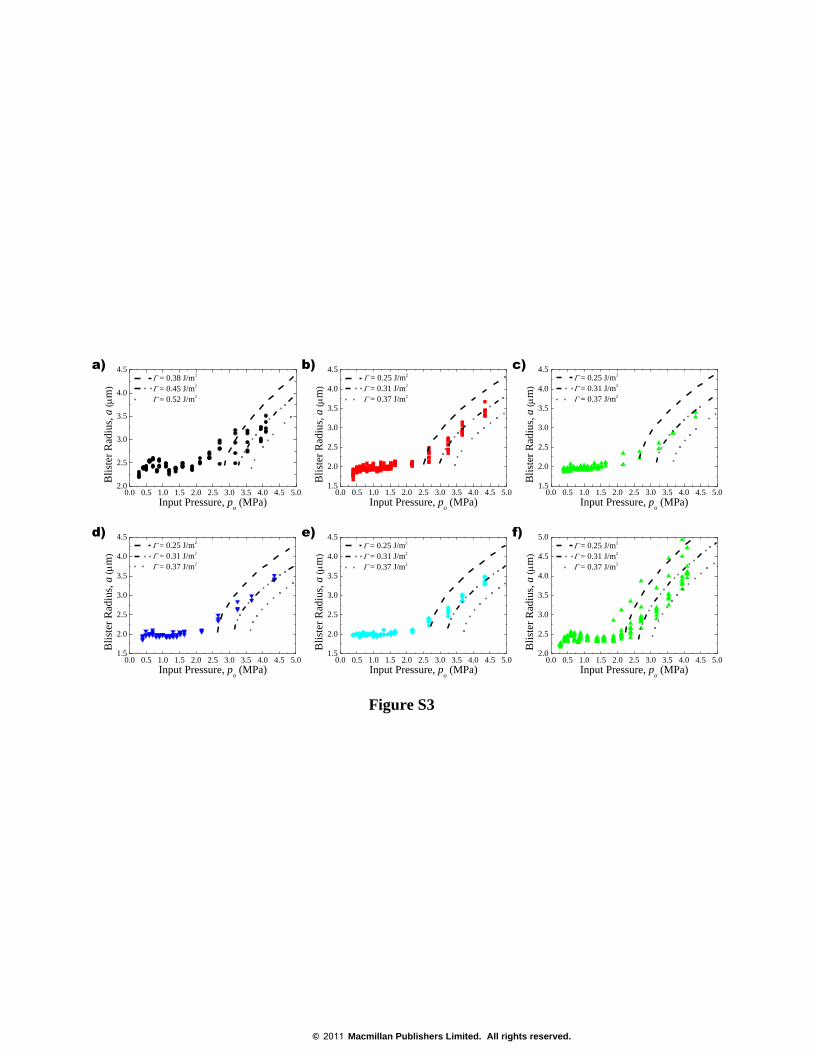
Figure S5. Repeatability of Measurements at Low Pressure Differences
(a) - (d) K(δ3/a
4) vs Δp for 2-5 layer devices. The black points are from the first
pressure cycling of the upper device in Fig. 1(a). After the highest pressure was
measured the pressure was allowed to decrease back to atmospheric pressure and
the measurements were repeated and carried higher pressures. This shows that up to
Δp ≈ 0.5 MPa there is no altering of the membrane properties between
measurements.
Figure S6. Measured Roughness of the Substrate
RMS roughness measurements taken by non-contact AFM of the substrate (0
layers), 1, 2, and 3 layers as well a thick graphene sample that was ~5 nm (~15
layers) thick as determined by the AFM. Error bars are ±1 standard deviation.
© 2011 Macmillan Publishers Limited. All rights reserved.
1300 1450 1600 1750 2400 2550 2700 28500.0
0.5
1.0
1.5
2.0
2.5
3.0
3.5
4.0
4.5
5.0
5.5
Inte
nsi
ty (
a.u
.)
Raman Shift (cm-1)
1 2 3 4 50.00
0.05
0.10
0.15
0.20
0.25
(G
)/(
Si)
Number of Layers
1300 1450 1600 1750 2400 2550 2700 28500.0
0.5
1.0
1.5
2.0
2.5
3.0
3.5
4.0
Inte
nsi
ty (
a.u
.)
Raman Shift (cm-1
)
1 2 3 4 50.00
0.05
0.10
0.15
0.20
0.25
(
G)/(
Si)
Number of Layers
a) c) e)
f) d) b)
Figure S1
© 2011 Macmillan Publishers Limited. All rights reserved.
0.0 0.5 1.0 1.5 2.0 2.5 3.0 3.5 4.0 4.5 5.0
75
150
225
300
375
450
525
600
675
= 0.38 J/m2
= 0.45 J/m2
= 0.52 J/m2
No Delamination
Max
imu
m D
efle
ctio
n, (
nm
)
Input Pressure, po (MPa)
0.0 0.5 1.0 1.5 2.0 2.5 3.0 3.5 4.0 4.5 5.0
75
150
225
300
375
450
525
600
675
= 0.25 J/m2
= 0.31 J/m2
= 0.37 J/m2
No Delamination
Max
imum
Def
lect
ion, (
nm
)
Input Pressure, po (MPa)
0.0 0.5 1.0 1.5 2.0 2.5 3.0 3.5 4.0 4.5 5.0
75
150
225
300
375
450
525
600
675
= 0.25 J/m2
= 0.31 J/m2
= 0.37 J/m2
No Delamination
Max
imu
m D
efle
ctio
n, (
nm
)
Input Pressure, po (MPa)
0.0 0.5 1.0 1.5 2.0 2.5 3.0 3.5 4.0 4.5 5.0
75
150
225
300
375
450
525
600
675
= 0.25 J/m2
= 0.31 J/m2
= 0.37 J/m2
No Delamination
Max
imu
m D
efle
ctio
n, (
nm
)
Input Pressure, po (MPa)
0.0 0.5 1.0 1.5 2.0 2.5 3.0 3.5 4.0 4.5 5.0
75
150
225
300
375
450
525
600
675
= 0.25 J/m2
= 0.31 J/m2
= 0.37 J/m2
No Delamination
Max
imum
Def
lect
ion, (
nm
)
Input Pressure, po (MPa)
0.0 0.5 1.0 1.5 2.0 2.5 3.0 3.5 4.0 4.5 5.0
75
150
225
300
375
450
525
600
675
= 0.25 J/m2
= 0.31 J/m2
= 0.37 J/m2
No Delamination
Max
imu
m D
efle
ctio
n, (
nm
)
Input Pressure, po (MPa)
a) b) c)
d) e) f)
Figure S2
© 2011 Macmillan Publishers Limited. All rights reserved.
0.0 0.5 1.0 1.5 2.0 2.5 3.0 3.5 4.0 4.5 5.02.0
2.5
3.0
3.5
4.0
4.5
= 0.38 J/m2
= 0.45 J/m2
= 0.52 J/m2
Bli
ster
Rad
ius,
a (
m)
Input Pressure, po (MPa)
0.0 0.5 1.0 1.5 2.0 2.5 3.0 3.5 4.0 4.5 5.01.5
2.0
2.5
3.0
3.5
4.0
4.5
= 0.25 J/m2
= 0.31 J/m2
= 0.37 J/m2
Bli
ster
Rad
ius,
a (
m)
Input Pressure, po (MPa)
0.0 0.5 1.0 1.5 2.0 2.5 3.0 3.5 4.0 4.5 5.01.5
2.0
2.5
3.0
3.5
4.0
4.5
= 0.25 J/m2
= 0.31 J/m2
= 0.37 J/m2
Bli
ster
Rad
ius,
a (
m)
Input Pressure, po (MPa)
0.0 0.5 1.0 1.5 2.0 2.5 3.0 3.5 4.0 4.5 5.01.5
2.0
2.5
3.0
3.5
4.0
4.5
= 0.25 J/m2
= 0.31 J/m2
= 0.37 J/m2
Bli
ster
Rad
ius,
a (
m)
Input Pressure, po (MPa)
0.0 0.5 1.0 1.5 2.0 2.5 3.0 3.5 4.0 4.5 5.01.5
2.0
2.5
3.0
3.5
4.0
4.5
= 0.25 J/m2
= 0.31 J/m2
= 0.37 J/m2
Bli
ster
Rad
ius,
a (
m)
Input Pressure, po (MPa)
0.0 0.5 1.0 1.5 2.0 2.5 3.0 3.5 4.0 4.5 5.02.0
2.5
3.0
3.5
4.0
4.5
5.0
= 0.25 J/m2
= 0.31 J/m2
= 0.37 J/m2
Bli
ster
Rad
ius,
a (
m)
Input Pressure, po (MPa)
a) b) c)
d) e) f)
Figure S3
© 2011 Macmillan Publishers Limited. All rights reserved.
0.0 0.5 1.0 1.5 2.0 2.5 3.0 3.5 4.0 4.5 5.00.0
0.5
1.0
1.5
2.0
2.5
3.0
Inte
rnal
Pre
ssu
re, p
int (
MP
a)
Input Pressure, po (MPa)
= 0.38 J/m2
= 0.45 J/m2
= 0.52 J/m2
No Delamination
0.0 0.5 1.0 1.5 2.0 2.5 3.0 3.5 4.0 4.5 5.00.0
0.5
1.0
1.5
2.0
2.5
3.0
Inte
rnal
Pre
ssure
, p
int (
MP
a)
Input Pressure, po (MPa)
= 0.25 J/m2
= 0.31 J/m2
= 0.37 J/m2
No Delamination
0.0 0.5 1.0 1.5 2.0 2.5 3.0 3.5 4.0 4.5 5.00.0
0.5
1.0
1.5
2.0
2.5
3.0
Inte
rnal
Pre
ssure
, p
int (
MP
a)
Input Pressure, po (MPa)
= 0.25 J/m2
= 0.31 J/m2
= 0.37 J/m2
No Delamination
0.0 0.5 1.0 1.5 2.0 2.5 3.0 3.5 4.0 4.5 5.00.0
0.5
1.0
1.5
2.0
2.5
3.0
Inte
rnal
Pre
ssure
, p
int (
MP
a)
Input Pressure, po (MPa)
= 0.25 J/m2
= 0.31 J/m2
= 0.37 J/m2
No Delamination
0.0 0.5 1.0 1.5 2.0 2.5 3.0 3.5 4.0 4.5 5.00.0
0.5
1.0
1.5
2.0
2.5
3.0
Inte
rnal
Pre
ssure
, p
int (
MP
a)
Input Pressure, po (MPa)
= 0.25 J/m2
= 0.31 J/m2
= 0.37 J/m2
No Delamination
0.0 0.5 1.0 1.5 2.0 2.5 3.0 3.5 4.0 4.5 5.00.0
0.5
1.0
1.5
2.0
2.5
3.0
Inte
rnal
Pre
ssure
, p
int (
MP
a)
Input Pressure, po (MPa)
= 0.25 J/m2
= 0.31 J/m2
= 0.37 J/m2
No Delamination
a) b) c)
d) e) f)
Figure S4
© 2011 Macmillan Publishers Limited. All rights reserved.
0.0 0.1 0.2 0.3 0.4 0.5 0.6 0.70
100
200
300
400
500
600
700
800
900
1000
1100
1200
Trial 1
Trial 2
Et = 694
K(
)3/a
4 (
m-1
)
p (MPa)
0.0 0.1 0.2 0.3 0.4 0.5 0.6 0.70
100
200
300
400
500
600
700
800
Trial 1
Trial 2
Et = 1041
K(
)3/a
4 (
m-1
)
p (MPa)
0.0 0.1 0.2 0.3 0.4 0.5 0.6 0.70
100
200
300
400
500
600
700
800
Trial 1
Trial 2
Et = 1388
K(
)3/a
4 (
m-1
)
p (MPa)
0.0 0.1 0.2 0.3 0.4 0.5 0.6 0.70
100
200
300
400
500
600
700
800
Trial 1
Trial 2
Et = 1735
K(
)3/a
4 (
m-1
)
p (MPa)
a) b)
d) e)
Figure S5
© 2011 Macmillan Publishers Limited. All rights reserved.
0 1 2 3 15120
130
140
150
160
170
180
190
200
210
RM
S R
ou
gh
nes
s (p
m)
Number of Layers
Figure S6
© 2011 Macmillan Publishers Limited. All rights reserved.