Embed Size (px)
Citation preview

PE43713Product SpecificationUltraCMOS® RF Digital Step Attenuator, 9 kHz–6 GHz
Features• Flexible attenuation steps of 0.25 dB, 0.5 dB and
1 dB up to 31.75 dB
• Glitch-less attenuation state transitions
• Monotonicity: 0.25 dB up to 4 GHz, 0.5 dB up to 5 GHz and 1 dB up to 6 GHz
• Extended +105 °C operating temperature
• Parallel and Serial programming interfaces with Serial Addressability
• Packaging—32-lead 5 × 5 mm QFN
Applications• Test and measurement (T&M)
• General purpose RF attenuator
Product DescriptionThe PE43713 is a 50Ω, HaRP™ technology-enhanced, 7-bit RF digital step attenuator (DSA) that supports a broad frequency range from 9 kHz to 6 GHz. It features glitch-less attenuation state transitions, supports 1.8V control voltage and includes an extended operating temperature range to +105 °C and optional VSS_EXT bypass mode to improve spurious performance, making this device ideal for test and measurement (T&M).
The PE43713 is a pin-compatible upgraded version of the PE43703. An integrated digital control interface supports both Serial Addressable and Parallel programming of the attenuation, including the capability to program an initial attenuation state at power-up.
The PE43713 covers a 31.75 dB attenuation range in 0.25 dB, 0.5 dB and 1dB steps. It is capable of maintaining 0.25 dB monotonicity through 4 GHz, 0.50 dB monotonicity through 5 GHz and 1 dB monotonicity through 6 GHz. In addition, no external blocking capacitors are required if 0 VDC is present on the RF ports.
The PE43713 is manufactured on Peregrine’s UltraCMOS® process, a patented variation of silicon-on-insulator (SOI) technology on a sapphire substrate.
Figure 1 • PE43713 Functional Diagram
×7
RFInput
RFOutput
Control Logic Interface
Switched Attenuator Array
VSS_EXTP/SA0 A1 A2
ParallelControl
Serial In
CLK
(optional)
LE
©2017, Peregrine Semiconductor Corporation. All rights reserved. • Headquarters: 9380 Carroll Park Drive, San Diego, CA, 92121
Product Specification DOC-84877-2 – (1/2018)www.psemi.com

PE43713UltraCMOS® RF Digital Step Attenuator
Peregrine’s HaRP technology enhancements deliver high linearity and excellent harmonics performance. It is an innovative feature of the UltraCMOS process, offering the performance of GaAs with the economy and integration of conventional CMOS.
Optional External VSS ControlFor proper operation, the VSS_EXT control pin must be grounded or tied to the VSS voltage specified in Table 2. When the VSS_EXT control pin is grounded, FETs in the switch are biased with an internal negative voltage generator. For applications that require the lowest possible spur performance, VSS_EXT can be applied externally to bypass the internal negative voltage generator.
Absolute Maximum RatingsExceeding absolute maximum ratings listed in Table 1 may cause permanent damage. Operation should be restricted to the limits in Table 2. Operation between operating range maximum and absolute maximum for extended periods may reduce reliability.
ESD PrecautionsWhen handling this UltraCMOS device, observe the same precautions as with any other ESD-sensitive devices. Although this device contains circuitry to protect it from damage due to ESD, precautions should be taken to avoid exceeding the rating specified in Table 1.
Latch-up ImmunityUnlike conventional CMOS devices, UltraCMOS devices are immune to latch-up.
Table 1 • Absolute Maximum Ratings for PE43713
Parameter/Condition Min Max Unit
Supply voltage, VDD –0.3 5.5 V
Digital input voltage –0.3 3.6 V
RF input power, 50Ω
9 kHz–48 MHz
>48 MHz–6 GHz
Figure 5+31
dBmdBm
Storage temperature range –65 +150 °C
ESD voltage HBM, all pins(1) 3000 V
ESD voltage CDM, all pins(2) 1000 V
Notes:
1) Human body model (MIL–STD 883 Method 3015).
2) Charged device model (JEDEC JESD22–C101).
Page 2 DOC-84877-2 – (1/2018)www.psemi.com

PE43713UltraCMOS® RF Digital Step Attenuator
Recommended Operating ConditionsTable 2 lists the recommending operating condition for the PE43713. Devices should not be operated outside the recommended operating conditions listed below.
Table 2 • Recommended Operating Condition for PE43713
Parameter Min Typ Max Unit
Normal mode, VSS_EXT = 0V(1)
Supply voltage, VDD 2.3 5.5 V
Supply current, IDD 150 200 µA
Bypass mode, VSS_EXT = –3.4V(2)
Supply voltage, VDD (VDD ≥ 3.4V see Table 3 for full spec compliance) 2.7 3.4 5.5 V
Supply current, IDD 50 80 µA
Negative supply voltage, VSS_EXT –3.6 –2.4 V
Negative supply current, ISS –40 –16 µA
Normal or bypass mode
Digital input high 1.17 3.6 V
Digital input low –0.3 0.6 V
Digital input current 17.5 µA
RF input power, CW(3)
9 kHz–48 MHz
>48 MHz–6 GHz
Figure 5+23
dBmdBm
RF input power, pulsed(4)
9 kHz–48 MHz
>48 MHz–6 GHz
Figure 5+28
dBmdBm
Operating temperature range –40 +25 +105 °C
Notes:
1) Normal mode: connect VSS_EXT (pin 20) to GND (VSS_EXT = 0V) to enable internal negative voltage generator.
2) Bypass mode: use VSS_EXT (pin 20) to bypass and disable internal negative voltage generator.
3) 100% duty cycle, all bands, 50Ω.
4) Pulsed, 5% duty cycle of 4620 µs period, 50Ω.
DOC-84877-2 – (1/2018) Page 3www.psemi.com

PE43713UltraCMOS® RF Digital Step Attenuator
Electrical SpecificationsTable 3 provides the PE43713 key electrical specifications at 25 °C, RF1 = RFIN, RF2 = RFOUT (ZS = ZL = 50Ω),
unless otherwise specified. Normal mode(1) is at VDD = 3.3V and VSS_EXT = 0V. Bypass mode(2) is at VDD = 3.4V and VSS_EXT = –3.4V.
Table 3 • PE43713 Electrical Specifications
Parameter Condition Frequency Min Typ Max Unit
Operating frequency 9 kHz 6 GHzAs
shown
Attenuation range
0.25 dB step
0.5 dB step
1 dB step
0–31.750–31.500–31.00
dBdBdB
Insertion loss
9 kHz–1.0 GHz1.0–2.2 GHz2.2–4.0 GHz4.0–6.0 GHz
1.31.6
1.952.45
1.51.852.42.8
dBdBdBdB
Attenuation error
0.25 dB step
0–8 dB 9 kHz–2.2 GHz±(0.20 + 1.5% of
attenuation setting)dB
8.25–31.75 dB 9 kHz–2.2 GHz±(0.20 + 2.0% of
attenuation setting)dB
0–31.75 dB >2.2–3.0 GHz±(0.15 + 3.0% of
attenuation setting)dB
0–31.75 dB >3.0–4.0 GHz±(0.25 + 3.5% of
attenuation setting)dB
0.5 dB step
0–8 dB 9 kHz–2.2 GHz±(0.20 + 1.5% of
attenuation setting)dB
8.5–31.5 dB 9 kHz–2.2 GHz±(0.20 + 2.0% of
attenuation setting)dB
0–31.5 dB >2.2–3.0 GHz±(0.15 + 3.0% of
attenuation setting)dB
0–31.5 dB >3.0–5.0 GHz±(0.25 + 5.0% of
attenuation setting)dB
Page 4 DOC-84877-2 – (1/2018)www.psemi.com
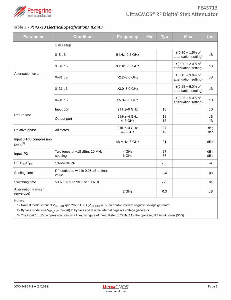
PE43713UltraCMOS® RF Digital Step Attenuator
Attenuation error
1 dB step
0–8 dB 9 kHz–2.2 GHz±(0.20 + 1.5% of
attenuation setting)dB
9–31 dB 9 kHz–2.2 GHz±(0.20 + 2.0% of
attenuation setting)dB
0–31 dB >2.2–3.0 GHz±(0.15 + 3.0% of
attenuation setting)dB
0–31 dB >3.0–5.0 GHz±(0.25 + 5.0% of
attenuation setting)dB
0–31 dB >5.0–6.0 GHz±(0.25 + 5.0% of
attenuation setting)dB
Return loss
Input port 9 kHz–6 GHz 18 dB
Output port9 kHz–4 GHz
4–6 GHz1315
dBdB
Relative phase All states9 kHz–4 GHz
4–6 GHz2742
degdeg
Input 0.1dB compression
point(3) 48 MHz–6 GHz 31 dBm
Input IP3Two tones at +18 dBm, 20 MHz spacing
4 GHz6 GHz
5756
dBmdBm
RF Trise/Tfall 10%/90% RF 200 ns
Settling timeRF settled to within 0.05 dB of final value
1.6 µs
Switching time 50% CTRL to 90% or 10% RF 275 ns
Attenuation transient (envelope)
2 GHz 0.3 dB
Notes:
1) Normal mode: connect VSS_EXT (pin 20) to GND (VSS_EXT = 0V) to enable internal negative voltage generator.
2) Bypass mode: use VSS_EXT (pin 20) to bypass and disable internal negative voltage generator.
3) The input 0.1 dB compression point is a linearity figure of merit. Refer to Table 2 for the operating RF input power (50Ω).
Table 3 • PE43713 Electrical Specifications (Cont.)
Parameter Condition Frequency Min Typ Max Unit
DOC-84877-2 – (1/2018) Page 5www.psemi.com

PE43713UltraCMOS® RF Digital Step Attenuator
Switching FrequencyThe PE43713 has a maximum 25 kHz switching rate in normal mode (pin 20 tied to ground). A faster switching rate is available in bypass mode (pin 20 tied to VSS_EXT). The rate at which the PE43713 can be switched is then limited to the switching time as specified in Table 3.
Switching frequency is defined to be the speed at which the DSA can be toggled across attenuation states. Switching time is the time duration between the point the control signal reaches 50% of the final value and the point the output signal reaches within 10% or 90% of its target value.
Spur-free PerformanceThe typical spurious performance of the PE43713 in normal mode is –130 dBm (pin 20 tied to ground). If spur-free performance is desired, the internal negative voltage generator can be disabled by applying a negative voltage to VSS_EXT (pin 20).
Glitch-less Attenuation State TransitionsThe PE43713 features a novel architecture to provide the best-in-class glitch-less transition behavior when changing attenuation states. When RF input power is applied, the output power spikes are greatly reduced (≤0.3 dB) during attenuation state changes when comparing to previous generations of DSAs.
Truth TablesTable 4–Table 6 provide the truth tables for the
PE43713.
Table 4 • Parallel Truth Table
Parallel Control Setting Attenuation Setting
RF1–RF2D6 D5 D4 D3 D2 D1 D0
L L L L L L L Reference IL
L L L L L L H 0.25 dB
L L L L L H L 0.5 dB
L L L L H L L 1 dB
L L L H L L L 2 dB
L L H L L L L 4 dB
L H L L L L L 8 dB
H L L L L L L 16 dB
H H H H H H H 31.75 dB
Table 5 • Serial Address Word Truth Table
Address WordAddressSettingA7
(MSB)A6 A5 A4 A3 A2 A1 A0
X X X X X L L L 000
X X X X X L L H 001
X X X X X L H L 010
X X X X X L H H 011
X X X X X H L L 100
X X X X X H L H 101
X X X X X H H L 110
X X X X X H H H 111
Table 6 • Serial Attenuation Word Truth Table
Attenuation Word Attenuation Setting
RF1–RF2D7 D6 D5 D4 D3 D2 D1D0
(LSB)
L L L L L L L L Reference IL
L L L L L L L H 0.25 dB
L L L L L L H L 0.5 dB
L L L L L H L L 1 dB
L L L L H L L L 2 dB
L L L H L L L L 4 dB
L L H L L L L L 8 dB
L H L L L L L L 16 dB
L H H H H H H H 31.75 dB
Table 4 • Parallel Truth Table (Cont.)
Parallel Control Setting Attenuation Setting
RF1–RF2D6 D5 D4 D3 D2 D1 D0
Page 6 DOC-84877-2 – (1/2018)www.psemi.com

PE43713UltraCMOS® RF Digital Step Attenuator
Serial Addressable Register MapFigure 2 provides the Serial Addressable register map for the PE43713.
Figure 2 • Serial Addressable Register Map
Attenuation Word
LSB (first in) MSB (last in)
Q7 Q6 Q5 Q4 Q3 Q2 Q1 Q0
D7 D6 D5 D4 D3 D2 D1 D0
Q15 Q14 Q13 Q12 Q11 Q10 Q9 Q8
A6 A7 A5 A4 A3 A2 A1 A0
Address Word
D7 must be set to logic low
Bits can either be set to logic high or logic low
4 × 18.25 = 73 73 → 01001001
Address Word: XXXXX011Attenuation Word: 01001001Serial Input: XXXXX01101001001
For example, to program the 18.25 dB state at address 3:
The attenuation word is derived directly from the value of the attenuation state. To find the attenuation word, multiply the value of the state by four, then convert to binary.
DOC-84877-2 – (1/2018) Page 7www.psemi.com

PE43713UltraCMOS® RF Digital Step Attenuator
Programming Options
Parallel/Serial SelectionEither a Parallel or Serial addressable interface can be used to control the PE43713. The P/S bit provides this selection, with P/S = LOW selecting the Parallel interface and P/S = HIGH selecting the Serial interface.
Parallel Mode InterfaceThe Parallel interface consists of seven CMOS-compatible control lines that select the desired attenu-ation state, as shown in Table 4.
The Parallel interface timing requirements are defined by Figure 4 (Parallel Interface Timing Diagram), Table 9 (Parallel and Direct Interface AC Character-istics) and switching time (Table 3).
For Latched Parallel programming, the Latch Enable (LE) should be held LOW while changing attenuation state control values then pulse LE HIGH to LOW (per Figure 4) to latch new attenuation state into the device.
For Direct Parallel programming, the LE line should be pulled HIGH. Changing attenuation state control values will change device state to new attenuation. Direct mode is ideal for manual control of the device (using hardwire, switches, or jumpers).
In parallel mode, Serial-In (SI) and Clock (CLK) pins are "don't care" and may be tied to logic LOW or logic HIGH.
Serial-Addressable InterfaceThe Serial-Addressable interface is a 16-bit Serial-In, Parallel-Out shift register buffered by a transparent latch. The 16-bits make up two words comprised of 8-bits each. The first word is the Attenuation Word, which controls the state of the DSA. The second word is the Address Word, which is compared to the static (or programmed) logical states of the A0, A1 and A2 digital inputs. If there is an address match, the DSA changes state; otherwise its current state will remain unchanged. Figure 3 illustrates an example timing diagram for programming a state. It is required that all Parallel control inputs be grounded when the DSA is used in Serial-Addressable mode.
The Serial-Addressable interface is controlled using three CMOS-compatible signals: SI, Clock (CLK) and
LE. The SI and CLK inputs allow data to be serially entered into the shift register. Serial data is clocked in LSB first.
The shift register must be loaded while LE is held LOW to prevent the attenuator value from changing as data is entered. The LE input should then be toggled HIGH and brought LOW again, latching the new data into the DSA. The Address Word truth table is listed in Table 5. The Attenuation Word truth table is listed in Table 6. A programming example of the serial register is illustrated in Figure 2. The serial timing diagram is illustrated in Figure 3.
Power-up Control SettingsThe PE43713 will always initialize to the maximum attenuation setting (31.75 dB) on power-up for both the Serial Addressable and Latched Parallel modes of operation and will remain in this setting until the user latches in the next programming word. In Direct Parallel mode, the DSA can be preset to any state within the 31.75 dB range by pre-setting the Parallel control pins prior to power-up. In this mode, there is a 400 µs delay between the time the DSA is powered-up to the time the desired state is set. During this power-up delay, the device attenuates to the maximum attenuation setting (31.75 dB) before defaulting to the user defined state. If the control pins are left floating in this mode during power-up, the device will default to the minimum attenuation setting (insertion loss state).
Dynamic operation between Serial and Parallel programming modes is possible.
If the DSA powers up in Serial mode (P/S = HIGH), all the Parallel control inputs DI[6:0] must be set to logic LOW. Prior to toggling to Parallel mode, the DSA must be programmed serially to ensure D[7] is set to logic LOW.
If the DSA powers up in either Latched or Direct Parallel mode, all Parallel pins DI[6:0] must be set to logic LOW prior to toggling to Serial Addressable mode (P/S = HIGH), and held LOW until the DSA has been programmed serially to ensure bit D[7] is set to logic LOW.
The sequencing is only required once on power-up. Once completed, the DSA may be toggled between Serial and Parallel programming modes at will.
Page 8 DOC-84877-2 – (1/2018)www.psemi.com

PE43713UltraCMOS® RF Digital Step Attenuator
Figure 3 • Serial Addressable Timing Diagram
Bits can either be set to logic high or logic lowSerial bit D[7] must be set to logic low
Parallel control inputsDI[6:0]
A[2] A[3] A[4] A[5] A[6] A[7]A[1]A[0]D[7]D[1] D[2] D[3] D[4] D[5] D[6]D[0]
Valid
TDISU
TASU
TPSSU
TSISU
TCLKL
TSIH
TCLKH
TDIH
TAH
TLESU
TPSIH
TLEPW
DI[6:0]
A[2:0]
P/S
SI
CLK
LE
Figure 4 • Latched-Parallel/Direct-Parallel Timing Diagram
TLEPW
TDIHTDISU
TPSIH
ValidDI[6:0]
LE
P/STPSSU
Parallel control inputsDI[6:0]
Table 7 • Latch and Clock Specifications
Latch Enable
Shift Clock Function
0 ↑ Shift register clocked
↑ XContents of shift register transferred to attenuator
core
DOC-84877-2 – (1/2018) Page 9www.psemi.com

PE43713UltraCMOS® RF Digital Step Attenuator
Table 8 • Serial Interface AC Characteristics(*)
Parameter/Condition Min Max Unit
Serial clock frequency, FCLK 10 MHz
Serial clock HIGH time, TCLKH 30 ns
Serial clock LOW time, TCLKL 30 ns
Last Serial clock rising edge setup time to Latch Enable rising edge, TLESU 10 ns
Latch Enable minimum pulse width, TLEPW 30 ns
Serial data setup time, TSISU 10 ns
Serial data hold time, TSIH 10 ns
Parallel data setup time, TDISU 100 ns
Parallel data hold time, TDIH 100 ns
Address setup time, TASU 100 ns
Address hold time, TAH 100 ns
Parallel/Serial setup time, TPSSU 100 ns
Parallel/Serial hold time, TPSIH 100 ns
Note: * VDD = 3.3V or 5.0V, –40 °C, < TA < +105 °C, unless otherwise specified.
Table 9 • Parallel and Direct Interface AC Characteristics(*)
Parameter/Condition Min Max Unit
Latch Enable minimum pulse width, TLEPW 30 ns
Parallel data setup time, TDISU 100 ns
Parallel data hold time, TDIH 100 ns
Parallel/Serial setup time, TPSSU 100 ns
Parallel/Serial hold time, TPSIH 100 ns
Note: * VDD = 3.3V or 5.0V, –40 °C < TA < +105 °C, unless otherwise specified.
Page 10 DOC-84877-2 – (1/2018)www.psemi.com

PE43713UltraCMOS® RF Digital Step Attenuator
Figure 5 • Power De-rating Curve, 9 kHz–6 GHz, –40 to +105 °C Ambient, 50Ω
579
11131517192123252729313335
0.01 0.05 0.50 5.00 50.00 500.00 5000.00
Max
imum
RF
Inpu
t Pow
er (d
Bm
)
Frequency (MHz)
P0.1 dB Compression (≥ 48 MHz) Pulsed (≥ 48 MHz)
CW & Pulsed (< 48 MHz) CW (≥ 48 MHz)
DOC-84877-2 – (1/2018) Page 11www.psemi.com

PE43713UltraCMOS® RF Digital Step Attenuator
Typical Performance DataFigure 6–Figure 32 show the typical performance data at 25 °C and VDD = 3.3V, RF1 = RFIN, RF2 = RFOUT (ZS = ZL = 50Ω) unless otherwise specified.
Figure 6 • Insertion Loss vs Temperature
-6
-5
-4
-3
-2
-1
0
0 1 2 3 4 5 6
Inse
rtio
n Lo
ss (d
B)
Frequency (GHz)
-40°C 25°C 85°C 105°C
Page 12 DOC-84877-2 – (1/2018)www.psemi.com

PE43713UltraCMOS® RF Digital Step Attenuator
Figure 7 • Input Return Loss vs Attenuation Setting
-45
-40
-35
-30
-25
-20
-15
-10
-5
0
0 1 2 3 4 5 6
Ret
urn
Loss
(dB
)
Frequency (dB)
0 dB 0.25 dB 0.5 dB 1 dB 2 dB
4 dB 8 dB 16 dB 28 dB 31.75 dB
Figure 8 • Output Return Loss vs Attenuation Setting
-50
-45
-40
-35
-30
-25
-20
-15
-10
-5
0
0 1 2 3 4 5 6
Ret
urn
Loss
(dB
)
Frequency (dB)
0 dB 0.25 dB 0.5 dB 1 dB 2 dB
4 dB 8 dB 16 dB 28 dB 31.75 dB
DOC-84877-2 – (1/2018) Page 13www.psemi.com

PE43713UltraCMOS® RF Digital Step Attenuator
Figure 9 • Input Return Loss for 16 dB Attenuation Setting vs Temperature
Figure 10 • Output Return Loss for 16 dB Attenuation Setting vs Temperature
-40
-35
-30
-25
-20
-15
-10
-5
0
0 1 2 3 4 5 6
Ret
urn
Loss
(dB
)
Frequency (GHz)
-40°C 25°C 85°C 105°C
-25
-20
-15
-10
-5
0
0 1 2 3 4 5 6
Ret
urn
Loss
(dB
)
Frequency (GHz)
-40°C 25°C 85°C 105°C
Page 14 DOC-84877-2 – (1/2018)www.psemi.com

PE43713UltraCMOS® RF Digital Step Attenuator
Figure 11 • Relative Phase Error vs Attenuation Setting
Figure 12 • Relative Phase Error for 31.75 dB Attenuation Setting vs Frequency
-10
0
10
20
30
40
50
60
0 1 2 3 4 5 6
Rel
ativ
e Ph
ase
Erro
r (dB
)
Frequency (GHz)
0 dB 0.25 dB 0.5 dB 1 dB 2 dB
4 dB 8 dB 16 dB 31.75 dB
0
10
20
30
40
50
60
-40C 25C 85C 105C
Rel
ativ
e Ph
ase
Erro
r (de
g)
Temperature (deg C)
0.9 GHz 1.8 GHz 2.2 GHz 3 GHz 4 GHz 5 GHz 6 GHz
DOC-84877-2 – (1/2018) Page 15www.psemi.com

PE43713UltraCMOS® RF Digital Step Attenuator
Figure 13 • Attenuation Error @ 900 MHz vs Temperature
Figure 14 • Attenuation Error @ 1800 MHz vs Temperature
-0.25
0
0.25
0.5
0.75
0 4 8 12 16 20 24 28 32
Atte
nuat
ion
Erro
r (dB
)
Attenuation Setting (dB)
-40°C 25°C 85°C 105°C
-0.25
0
0.25
0.5
0.75
0 4 8 12 16 20 24 28 32
Atte
nuat
ion
Erro
r (dB
)
Attenuation Setting (dB)
-40°C 25°C 85°C 105°C
Page 16 DOC-84877-2 – (1/2018)www.psemi.com

PE43713UltraCMOS® RF Digital Step Attenuator
Figure 15 • Attenuation Error @ 2200 MHz vs Temperature
Figure 16 • Attenuation Error @ 3000 MHz vs Temperature
-0.25
0
0.25
0.5
0.75
0 4 8 12 16 20 24 28 32
Atte
nuat
ion
Erro
r (dB
)
Attenuation Setting (dB)
-40°C 25°C 85°C 105°C
-0.25
0
0.25
0.5
0.75
0 4 8 12 16 20 24 28 32
Atte
nuat
ion
Erro
r (dB
)
Attenuation Setting (dB)
-40°C 25°C 85°C 105°C
DOC-84877-2 – (1/2018) Page 17www.psemi.com

PE43713UltraCMOS® RF Digital Step Attenuator
Figure 17 • Attenuation Error @ 4000 MHz vs Temperature
Figure 18 • IIP3 vs Attenuation Setting
0
0.25
0.5
0.75
1
0 4 8 12 16 20 24 28 32
Atte
nuat
ion
Erro
r (dB
)
Attenuation Setting (dB)
-40°C 25°C 85°C 105°C
50
55
60
65
70
3 4 5 6
Inpu
t IP3
(dB
)
Frequency (GHz)
0 dB 3.5 dB 7.5 dB 11 dB 14 dB
17.5 dB 21.5 dB 24.75 dB 28 dB 31.75 dB
Page 18 DOC-84877-2 – (1/2018)www.psemi.com
PE43713UltraCMOS® RF Digital Step Attenuator
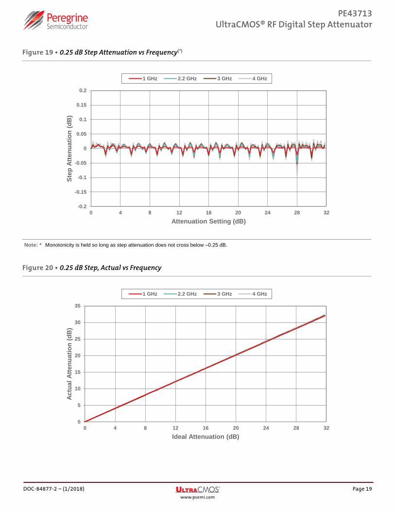
Figure 19 • 0.25 dB Step Attenuation vs Frequency(*)
Note: * Monotonicity is held so long as step attenuation does not cross below –0.25 dB.
Figure 20 • 0.25 dB Step, Actual vs Frequency
-0.2
-0.15
-0.1
-0.05
0
0.05
0.1
0.15
0.2
0 4 8 12 16 20 24 28 32
Step
Atte
nuat
ion
(dB
)
Attenuation Setting (dB)
1 GHz 2.2 GHz 3 GHz 4 GHz
0
5
10
15
20
25
30
35
0 4 8 12 16 20 24 28 32
Actu
al A
ttenu
atio
n (d
B)
Ideal Attenuation (dB)
1 GHz 2.2 GHz 3 GHz 4 GHz
DOC-84877-2 – (1/2018) Page 19www.psemi.com

PE43713UltraCMOS® RF Digital Step Attenuator
Figure 21 • 0.25 dB Major State Bit Error vs Attenuation Setting
Figure 22 • 0.25 dB Attenuation Error vs Frequency
-0.4
-0.2
0
0.2
0.4
0.6
0.8
1
0 1 2 3 4
Atte
nuat
ion
Erro
r (dB
)
Frequency (GHz)
0.25 dB 0.5 dB 1 dB 2 dB 4 dB 8 dB 16 dB 31.75 dB
-0.4
-0.2
0
0.2
0.4
0.6
0.8
1
0 4 8 12 16 20 24 28 32
Atte
nuat
ion
Erro
r (dB
)
Attenuation Setting (dB)
1 GHz 2.2 GHz 3 GHz 4 GHz
Page 20 DOC-84877-2 – (1/2018)www.psemi.com

PE43713UltraCMOS® RF Digital Step Attenuator
Figure 23 • 0.5 dB Step Attenuation vs Frequency(*)
Note: * Monotonicity is held so long as step attenuation does not cross below –0.5 dB.
Figure 24 • 0.5 dB Step, Actual vs Frequency
-0.2
-0.15
-0.1
-0.05
0
0.05
0.1
0.15
0.2
0 4 8 12 16 20 24 28 32
Step
Atte
nuat
ion
(dB
)
Attenuation Setting (dB)
1 GHz 2.2 GHz 3 GHz 4 GHz 5 GHz
0
5
10
15
20
25
30
35
0 4 8 12 16 20 24 28 32
Actu
al A
ttenu
atio
n (d
B)
Ideal Attenuation (dB)
1 GHz 2.2 GHz 3 GHz 4 GHz 5 GHz
DOC-84877-2 – (1/2018) Page 21www.psemi.com

PE43713UltraCMOS® RF Digital Step Attenuator
Figure 25 • 0.5 dB Major State Bit Error vs Attenuation Setting
Figure 26 • 0.5 dB Attenuation Error vs Frequency
-0.2
0
0.2
0.4
0.6
0.8
1
1.2
0 1 2 3 4 5
Atte
nuat
ion
Erro
r (dB
)
Frequency (GHz)
0.5 dB 1 dB 2 dB 4 dB 8 dB 16 dB 31.5 dB
-0.2
0
0.2
0.4
0.6
0.8
1
1.2
0 4 8 12 16 20 24 28 32
Atte
nuat
ion
Erro
r (dB
)
Attenuation Setting (dB)
1 GHz 2.2 GHz 3 GHz 4 GHz 5 GHz
Page 22 DOC-84877-2 – (1/2018)www.psemi.com

PE43713UltraCMOS® RF Digital Step Attenuator
Figure 27 • 1 dB Step Attenuation vs Frequency(*)
Note: * Monotonicity is held so long as step attenuation does not cross below –1 dB.
Figure 28 • 1 dB Step, Actual vs Frequency
-0.25
-0.2
-0.15
-0.1
-0.05
0
0.05
0.1
0.15
0.2
0.25
0 4 8 12 16 20 24 28 32
Step
Atte
nuat
ion
(dB
)
Attenuation Setting (dB)
1 GHz 2.2 GHz 3 GHz 4 GHz 5 GHz 6 GHz
0
5
10
15
20
25
30
35
0 4 8 12 16 20 24 28 32
Actu
al A
ttenu
atio
n (d
B)
Ideal Attenuation (dB)
1 GHz 2.2 GHz 3 GHz 4 GHz 5 GHz 6 GHz
DOC-84877-2 – (1/2018) Page 23www.psemi.com

PE43713UltraCMOS® RF Digital Step Attenuator
Figure 29 • 1 dB Major State Bit Error vs Attenuation Setting
Figure 30 • 1 dB Attenuation Error vs Frequency
-0.2
0
0.2
0.4
0.6
0.8
1
1.2
0 1 2 3 4 5 6
Atte
nuat
ion
Erro
r (dB
)
Frequency (GHz)
1 dB 2 dB 4 dB 8 dB 16 dB 31 dB
-0.2
0
0.2
0.4
0.6
0.8
1
1.2
0 4 8 12 16 20 24 28 32
Atte
nuat
ion
Erro
r (dB
)
Attenuation Setting (dB)
1 GHz 2.2 GHz 3 GHz 4 GHz 5 GHz 6 GHz
Page 24 DOC-84877-2 – (1/2018)www.psemi.com

PE43713UltraCMOS® RF Digital Step Attenuator
Figure 31 • Attenuation Transient (15.75–16 dB), Typical Switching Time = 275 ns
Figure 32 • Attenuation Transient (16–15.75 dB), Typical Switching Time = 275 ns
-17.0
-16.8
-16.6
-16.4
-16.2
-16.0
-15.8
-15.6
-15.4
0 400 800 1200 1600 2000 2400 2800 3200
Enve
lope
Pow
er (d
Bm
)
Time (ns)
Power (dBm)
Trigger starts ~730 ns
Glitch = 0.15 dB
-17.0
-16.8
-16.6
-16.4
-16.2
-16.0
-15.8
-15.6
-15.4
0 400 800 1200 1600 2000 2400 2800 3200
Enve
lope
Pow
er (d
Bm
)
Time (ns)
Power (dBm)
Trigger starts ~730 ns
Glitch = 0.03 dB
DOC-84877-2 – (1/2018) Page 25www.psemi.com

PE43713UltraCMOS® RF Digital Step Attenuator
Evaluation Kit The digital step attenuator evaluation board (EVB) was designed to ease customer evaluation of the PE43713 digital step attenuator. The PE43713 EVB supports Direct Parallel, Latched Parallel and Serial modes.
Evaluation Kit SetupConnect the EVB with the USB dongle board and USB cable as shown in Figure 33.
Direct Parallel Programming ProcedureDirect Parallel programming is suitable for manual operation without software programming. For manual Direct Parallel programming, position the Parallel/Serial (P/S) select switch to the Parallel position. The LE switch must be switched to HIGH position. Switches D0–D6 are SP3T switches that enable the user to manually program the parallel bits. When D0–D6 are toggled to the HIGH position, logic high is presented to the parallel input. When toggled to the LOW position, logic low is presented to the parallel input. Setting LE and D0–D6 to the EXT position presents as OPEN, which is set for software programming of Latched Parallel and Serial modes. Table 4 depicts the Parallel truth table.
Latched Parallel Programming ProcedureFor automated Latched Parallel programming, connect the USB dongle board and cable that is provided with the evaluation kit (EVK) from the USB
port of the PC to the J5 header of the PE43713 EVB, and set the LE and D0–D6 SP3T switches to the EXT position. Position the Parallel/Serial (P/S) select switch to the Parallel position. The evaluation software is written to operate the DSA in Parallel mode. Ensure that the software GUI is set to Latched Parallel mode. Use the software GUI to enable the desired attenuation state. The software GUI automati-cally programs the DSA each time an attenuation state is enabled.
Serial Addressable Programming ProcedureFor automated Serial programming, connect the USB dongle board and cable that is provided with the EVK from the USB port of the PC to the J5 header of the PE43713 EVB, and set the LE and D0–D6 SP3T switches to the EXT position. Position the Parallel/Serial (P/S) select switch to the Serial position. Prior to programming, the user must define an address setting using the HDR2 header pin. Jump the middle column of pins on the HDR2 header (A0–A2) to the left column of pins to set logic LOW, or jump the middle row of pins to the right column of pins to set logic HIGH. If the HDR2 pins are left open, then 000 becomes the default address. The software GUI is written to operate the DSA in Serial mode. Use the software GUI to enable each setting to the desired attenuation state. The software GUI automatically programs the DSA each time an attenuation state is enabled.
Figure 33 • Evaluation Kit for PE43713
Page 26 DOC-84877-2 – (1/2018)www.psemi.com

PE43713UltraCMOS® RF Digital Step Attenuator
Figure 34 • Evaluation Kit Layout for PE43713
DOC-84877-2 – (1/2018) Page 27www.psemi.com

PE43713UltraCMOS® RF Digital Step Attenuator
Pin InformationThis section provides pinout information for the PE43713. Figure 35 shows the pin map of this device for the available package. Table 10 provides a description for each pin.
Figure 35 • Pin Configuration (Top View)
ExposedGround Pad
CLK
C8
C16
SI
GN
DG
ND
GN
D
C2
C1
C0.
5C
0.25
GN
DG
ND
GN
D
A1A2VSS_EXT
GNDRF2GND
GN
D
LEGND
P/SA0
GNDGNDRF1
GND
VDD
1
3
4
5
6
7
8
2
9 11 12 13 14 15 1610
32 30 29 28 27 26 2531
24
22
21
20
19
18
17
23
C4
GN
D
Pin 1 DotMarking
Table 10 • Pin Descriptions for PE43713
Pin No. Pin Name Description
1, 5, 6, 8–17, 19
GND Ground
2 VDD Supply voltage
3 P/S Serial/Parallel mode select
4 A0 Address bit A0 connection
7 RF1(1) RF1 port (RF input)
18 RF2(1) RF2 port (RF output)
20 VSS_EXT(2)
External VSS negative voltage con-
trol
21 A2 Address bit A2 connection
22 A1 Address bit A1 connection
23 LE Serial interface Latch Enable input
24 CLK Serial interface Clock input
25 SI Serial interface Data input
26 C16 (D6)(3) Parallel control bit, 16 dB
27 C8 (D5)(3) Parallel control bit, 8 dB
28 C4 (D4)(3) Parallel control bit, 4 dB
29 C2 (D3)(3) Parallel control bit, 2 dB
30 C1 (D2)(3) Parallel control bit, 1 dB
31 C0.5 (D1)(3) Parallel control bit, 0.5 dB
32 C0.25 (D0)(3) Parallel control bit, 0.25 dB
Pad GNDExposed pad: ground for proper operation
Notes:
1) RF pins 7 and 18 must be at 0 VDC. The RF pins do not require DC blocking capacitors for proper operation if the 0 VDC requirement is met.
2) Use VSS_EXT (pin 20) to bypass and disable internal negative
voltage generator. Connect VSS_EXT (pin 20) to GND (VSS_EXT =
0V) to enable internal negative voltage generator.
3) Ground C0.25, C0.5, C1, C2, C4, C8 and C16 if not in use.
Page 28 DOC-84877-2 – (1/2018)www.psemi.com

PE43713UltraCMOS® RF Digital Step Attenuator
Packaging InformationThis section provides packaging data including the moisture sensitivity level, package drawing, package marking and tape-and-reel information.
Moisture Sensitivity LevelThe moisture sensitivity level rating for the PE43713 in the 32-lead 5 × 5 mm QFN package is MSL1.
Package Drawing
Top-Marking Specification
Figure 36 • Package Mechanical Drawing for 32-lead 5 × 5 × 0.85 mm QFN
Figure 37 • Package Marking Specifications for PE43713
TOP VIEW BOTTOM VIEW
SIDE VIEW
RECOMMENDED LAND PATTERN
A0.10 C
(2X)
C
0.10 C
0.05 CSEATING PLANE
B
0.10 C
(2X)
0.10 C A B0.05 C
ALL FEATURES
PIN #1 CORNER
5.00
5.000.40±0.05
(x32)
3.10±0.05
0.25±0.05(x32)
0.50
3.50REF
3.10±0.05
0.85±0.05
0.05REF0.203
REF
(x28)
CHAMFER0.35 x 45°
0.30(x32)
0.60(x32)
3.15
3.15
5.40
5.40
0.50(x28)
189
32
17 24
2516
=YY =WW =
ZZZZZZZ =
Pin 1 indicatorLast two digits of assembly yearAssembly work weekAssembly lot code (maximum seven characters)
43713YYWW
ZZZZZZZ
DOC-84877-2 – (1/2018) Page 29www.psemi.com
PE43713UltraCMOS® RF Digital Step Attenuator
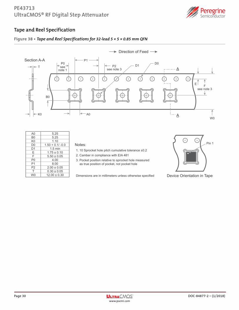
Tape and Reel SpecificationPE43713
Figure 38 • Tape and Reel Specifications for 32-lead 5 × 5 × 0.85 mm QFN
Device Orientation in Tape
Pin 1
T
K0 A0
B0
P0P1
D1A
Section A-A
A
Direction of Feed
D0
E
W0
P2see note 3
seenote 1
Fsee note 3
A0B0K0D0D1EF
P0P1P2T
W0
5.255.251.10
1.50 + 0.1/ -0.01.5 min
1.75 ± 0.105.50 ± 0.05
4.008.00
2.00 ± 0.050.30 ± 0.0512.00 ± 0.30
Notes:1. 10 Sprocket hole pitch cumulative tolerance ±0.22. Camber in compliance with EIA 4813. Pocket position relative to sprocket hole measured
as true position of pocket, not pocket hole
Dimensions are in millimeters unless otherwise specified
Page 30 DOC-84877-2 – (1/2018)www.psemi.com

PE43713
Ordering InformationTable 11 lists the available ordering codes for the PE43713 as well as available shipping methods.
Table 11 • Order Codes for PE43713
Order Codes Description Packaging Shipping Method
PE43713A-Z PE43713 Digital step attenuator Green 32-lead 5 × 5 mm QFN 3000 units / T&R
PE43713B-Z PE43713 Digital step attenuator Green 32-lead 5 × 5 mm QFN 3000 units / T&R
EK43713-02 PE43713 Evaluation kit Evaluation kit 1 / Box
EK43713-03 PE43713 Evaluation kit Evaluation kit 1 / Box
Product Specification www.psemi.com DOC-84877-2 – (1/2018)
Document CategoriesAdvance InformationThe product is in a formative or design stage. The datasheet contains design target specifications for product development. Specifications andfeatures may change in any manner without notice.
Preliminary SpecificationThe datasheet contains preliminary data. Additional data may be added at a later date. Peregrine reserves the right to change specifications at anytime without notice in order to supply the best possible product.
Product SpecificationThe datasheet contains final data. In the event Peregrine decides to change the specifications, Peregrine will notify customers of the intendedchanges by issuing a CNF (Customer Notification Form).
Sales ContactFor additional information, contact Sales at [email protected].
DisclaimersThe information in this document is believed to be reliable. However, Peregrine assumes no liability for the use of this information. Use shall beentirely at the user’s own risk. No patent rights or licenses to any circuits described in this document are implied or granted to any third party.Peregrine’s products are not designed or intended for use in devices or systems intended for surgical implant, or in other applications intended tosupport or sustain life, or in any application in which the failure of the Peregrine product could create a situation in which personal injury or deathmight occur. Peregrine assumes no liability for damages, including consequential or incidental damages, arising out of the use of its products insuch applications.
Patent StatementPeregrine products are protected under one or more of the following U.S. patents: patents.psemi.com
Copyright and Trademark©2017, Peregrine Semiconductor Corporation. All rights reserved. The Peregrine name, logo, UTSi and UltraCMOS are registered trademarks andHaRP, MultiSwitch and DuNE are trademarks of Peregrine Semiconductor Corp.