Embed Size (px)
Citation preview
Ultrafast Neuromorphic Photonic Image Processing with a VCSEL Neuron Joshua Robertson*, Paul Kirkland, Juan Arturo Alanis, Matěj Hejda, Julián Bueno, Gaetano Di Caterina & Antonio Hurtado
The ever-increasing demand for Artificial Intelligence (AI) systems is underlining a significant requirement for new, AI-optimised hardware. Neuromorphic (brain-like) processors are one highly-promising solution, with photonic-enabled realizations receiving increasing attention. Among these, approaches based upon Vertical Cavity Surface Emitting Lasers (VCSELs) are attracting interest given their favourable attributes and mature technology. Here, we demonstrate a hardware-friendly neuromorphic photonic spike processor, using a single VCSEL, for all-optical image edge-feature detection. This exploits the ability of a VCSEL-based photonic neuron to integrate temporally-encoded pixel data at high speed; and fire fast (100ps-long) optical spikes upon detecting desired image features. Furthermore, the photonic system is combined with a software-implemented spiking neural network yielding a full platform for complex image classification tasks. This work therefore highlights the potentials of VCSEL-based platforms for novel, ultrafast, all-optical neuromorphic processors interfacing with current computation and communication systems for use in future light-enabled AI and computer vision functionalities.
Introduction
A direct result of the vast uptake of internet-connected devices is the growing availability of data and
the increasing demand for faster, more efficient data processing platforms. Electronic processing
technologies have grown to alleviate some of this demand [1-3], demonstrating high computational
throughput and enabling the development of novel systems for artificial intelligence (AI) [4]. However,
less traditional computing approaches, such as those based on neuromorphic (brain-inspired) processing
elements, have also risen in popularity [5,6]. These systems, that have thrived in electronics, have
demonstrated highly parallel architectures and impressive decision-making capability. Nevertheless, like
their more traditional processing counterparts, the performance increment of silicon-based platforms is
becoming increasingly limited due to fundamental physical challenges in electronic technologies [7].
Crosstalk, parasitic capacitance, and Joule-heating each contribute to the limitation of the speed,
bandwidth, footprint, and efficiency of electronic systems, in turn driving many researchers to
investigate alternative platforms for future data processing systems.
One such alternative platform is photonics. Photonic light-based systems boast features such as
increased bandwidth, high energy efficiency, low cross talk and fast operation speeds, helping remedy
some of the limitations posed to advancing electronics. Recently, investigations into photonic Artificial
Neural Networks (ANNs) and neuromorphic systems have been on the rise. Optical devices, such as
quantum resonant tunnelling (QRT) structures [8-10], optical modulators [11], phase-change materials
(PCMs) [12] and semiconductor lasers (SLs) [13-17], to name a few, have all been investigated as
candidates for novel neuromorphic photonic processing systems. Yet with the field still in its infancy,
some investigations have already flourished into efforts to accelerate information processing in
photonics with ANNs [18-20], and reservoir computing systems [21-22]. Similarly, Convolutional
Neural Networks (CNNs), which have shown great success in the fields of image processing and

computer vision, are also seeing implementation on photonic platforms. Devices such as PCMs [23],
micro-ring weighting banks [24] and modulators [25] have been proposed to improve the speed and
efficiency of the computationally expensive convolution operations.
Like in classical ANNs, there are a number of processing tasks to which neuromorphic
computing systems are particularly applicable, one being the classification and recognition of images
and patterns. Software implemented neuromorphic Spiking Neural Networks (SNNs), similarly to
CNNs, have demonstrated successful image processing functionalities. Such SNN systems have applied
combinations of convolution and pooling techniques to extract image features [27], and have been used
in conjunction with dynamic vision sensor (DVS) cameras [28] and single photon avalanche detectors
(SPADs) [29] to perform image processing tasks. Further, reports have also shown that SNNs have lower
energy operational requirements and produce lower latency than CNNs, due to only the active parts of
the network requiring computation [30]. Therefore, SNNs made up of neuromorphic photonic devices
(as reported theoretically in [31]), exhibit great potentials for the future development of fast and efficient
image processing systems built directly on optical platforms.
Alongside these efforts, SLs have shown the ability to operate as high-speed artificial optical
spiking neurons, emulating the functionality and spiking operation of biological neurons in the brain
(see [26] and references therein for a review). Among SLs, vertical cavity surface emitting lasers
(VCSELs) have attracted considerable attention given their unique attributes (e.g. high speed, ease to
integrate in 2D arrays, low energy operation, high coupling efficiency to optical fibres, etc.). A number
of neuronal functionalities have been recently demonstrated in VCSELs, including ultrafast spike
activation and inhibition [32], networked spiking communication [33], spike rate encoding [34] and
pattern recognition [35], to name a few. Furthermore, theoretical spin flip model (SFM) studies [36]
indicate that VCSELs have the potential to present a pathway to unsupervised learning, via the neuron-
inspired spike-timing dependent plasticity (STDP) technique. Also very recently, the authors have
outlined the potentials of VCSEL neurons for image processing [37-38] and encoding functionalities
[39]. However, in these early image processing reports, the VCSEL neurons acted as spike thresholding
elements, requiring the image pixel information to be pre-processed offline.
This work overcomes this key challenge, demonstrating a photonic VCSEL-based hardware
system and all-optical spiking convolutional operation for image processing functionalities. The
proposed platform uses a single VCSEL acting as an artificial optical spiking neuron, in combination
with time-division multiplexing to allow for an extremely hardware friendly platform. The integrate-
and-fire capability of the spiking VCSEL neuron is exploited to simultaneously process multiple high-
speed optical inputs (100ps-long), each encoding distinct image pixels to deliver spiking convolutional
operation directly in the optical domain. This feature is used in this work to demonstrate all-optical edge-
feature detection in (complex) source images at very high speed and with noise robust operation. We
demonstrate successful edge feature detection for a variety of source images, including complex images
(e.g. the logo of our Institute) as well as type-written and hand-written digits (5000 images from the
MNIST database). Moreover, we show that the optical spiking outputs from the VCSEL-based
neuromorphic photonic hardware system can be fed to software implemented SNNs to demonstrate
successful hand-written digit image recognition. Additionally, our approach uses inexpensive and
commercially-sourced VCSELs working at the key telecom wavelength of 1550 nm, hence permitting
full compatibility with optical communication networks and data centre technologies.
Results Spiking Image Edge Detection with a VCSEL Neuron. In this work, we utilize the
neuromorphic functionalities of VCSELs, in tandem with convolution, to perform image processing
tasks. Specifically, we will tap into the input integration functionality of the VCSEL neuron that allows
the device to temporally summate the energy contribution of multiple fast (100ps-long) input pulses
occurring in quick succession [35]. Known in biological neuronal model as integration, this key
processing functionality permits neurons to receive multiple input signals (through dendrite receptors)
from different neurons in a network, integrate their combined intensity (in the neuron’s body or soma)

and fire spiking responses (once the threshold for spike firing is exceeded) that are communicated to
neighbouring neurons (via its axon). Here, we capitalise on the optical integration capability of our
VCSEL neuron, alongside its ability to threshold inputs and activate fast sub-ns spiking responses, to
develop a novel optical approach to image edge detection [37].
Fig. 1. Image processing technique with a spiking VCSEL neuron. Diagrams of a biological (a) and an artificial
optical VCSEL neuron (b), illustrating the integration of multiple inputs and spike firing upon a threshold-exceeding
input. Schematic of the image convolution and input generation process (c). Source images are converted into binary
matrices, 1’s (black) and -1’s (white) and operated on by a 2x2 kernel operator creating a Hadamard (elementwise)
product. The product is used for the generation of a return-to-zero (RZ) image input, where each pixel is given a
configurable duration. The kernel operator is scanned across the image, time-multiplexing the inputs generated for
each pixel. Experimental setup (d). The image input data is generated by an arbitrary waveform generator (AWG)
and encoded, using a Mach Zehnder intensity modulator (MZ), into the light of a tuneable laser (TL). The injection
light from the TL is directed into the VCSEL neuron using fibre-optic components; these include optical isolators
(ISO), variable optical attenuators (VOA), polarisation controllers (PCs) and circulators (CIRC). The VCSEL
neuron’s response is analysed with a fast real time oscilloscope (OSC) after detection with a photodiode (PD).
In this new technique, image edge feature detection is performed according to the depiction
illustrated in Fig. 1 (see methods section and supplementary information for full details). Fig. 2 shows
experimental results on the edge-detection of a printed “Digit 4” 32x32 pixel source image. Here, 8
different (2x2) kernel operators are run sequentially. These kernels apply integer weights, 1 for black
and -1 for white, to the image’s pixel data. As 2x2 kernels are used here to process each pixel, 4 input
values are required. These are encoded using 4 time-multiplexed 100 ps pulses. A total time of 3 ns per

pixel was selected in the experiments and all pixel information is serialised before its injection into the
VCSEL neuron.
First, two ‘vertical’ 2x2 kernels are applied to the source image triggering different spiking
responses from the VCSEL neuron. These are captured using a real time oscilloscope and analysed using
temporal maps, which de-multiplex the captured timeseries to form reconstructed images. Next, 3.0 ns
segments (the configured pixel window) are sampled from the temporal maps to reveal which pixel
inputs had activated spiking responses. A black pixel is plotted in a final image reconstruction when a
spike activation (target feature) is detected. The convolution results for both vertical kernels are shown
in final reconstruction of Figs. 2(c)-(d), revealing that the vertical edges of the “Digit 4” are identified
by the VCSEL neuron (firing 100ps-long spikes). To achieve this result, the ‘vertical’ kernels yield
bursts of 4 negative input pulses when a vertical edge feature is found in the image, and smaller input
pulse bursts for all other pixel features (see supplementary information). The VCSEL neuron integrates
the combined energy of these time-multiplexed bursts, only firing a spike when all four pulses are
negative (the total energy goes beyond the spike firing threshold) to detect a vertical edge in the image.
For all other cases, the VCSEL neuron remains quiescent as the combined energy of the encoded input
burst does not exceed the spike activation threshold.
Fig. 2. Spike edge-feature detection of a black-and-white image with a VCSEL neuron. The 32x32 pixel source
image (a) and reconstructed image (b) of a printed “Digit 4” after it’s operated on by 8 different 2x2 kernels. Plots
(c)-(j) depict individual results achieved for each of the 8 2x2 kernel operators utilised. These are shown in the insets
below plots (c-j) and are respectively: two vertical (c)-(d), two horizontal (e)-(f), and four diagonal (g)-(j) kernel
operators. Each black dot in plots (b-j) corresponds to a 100ps-long long spike fired by the VCSEL neuron upon
recognising a specific feature in the source image. The final 8 kernel reconstruction reveals all edges in the image.
In Figs. 2(e)-(f), we apply 2x2 ‘horizontal’ kernel operators to detect the horizontal edge-
features in the printed ‘Digit 4’ image. The ‘horizontal’ kernels again apply integer weights to the source
image pixel data. The VCSEL neuron correctly reveals all horizontal features present in the image with
the firing of fast sub-ns spikes. Additional kernel operators are applied to reveal the diagonal edges of
the image. These are set with the following non-integer weights: 0.5, 0.75, 0.75 and -1 and the three
rotations. The results of the diagonal integrate-and-fire convolutions are shown in Figs. 2(g)-(j),
revealing successful detection of all diagonal features (Figs. 2(g)-(h)) as well as corner-features (Figs.
2(i)-(j)). Combining all eight experimental runs, we can form a single (8-kernel) reconstruction of the
image revealing all edge information, as shown in Fig. 2(b). The technique presented here uses a single
spiking VCSEL neuron combined with time-multiplexing and is therefore capable of providing all-
optical edge detection functionality.

To further test the capability of our system we selected a source image of higher complexity,
namely a 323x323 pixel RGB image of the University of Strathclyde’s (UoS’s) crest (Fig. 3(a)). This
higher resolution image had three colour channels, red, green and blue. In this demonstration the green
channel was selected before conversion into binarized black and white (Fig. 3(b)). We then used the
same process and the same 8 kernel operators as in Fig. 2, to detect and reveal the image’s edge features
through the sub-ns spiking of the VCSEL neuron. The spiking time-series obtained with the 8 different
2x2 kernel operators are combined into the reconstructed image plotted in Fig. 3(c). The latter shows
that all horizontal, vertical and diagonal lines were recognised; hence illustrating that neither image size
nor complexity impede the operation of the photonic spiking VCSEL-based edge detection system.
Importantly, an overall edge detection accuracy of 96.63% was achieved. A configurable pixel duration
equal to 3.0 ns was set in all cases analysed in Figs. 2 and 3. Hence, our approach permits ultrafast image
processing. For example, the time required to process the large 322 x 322 pixel UoS’ crest image of Fig.
3 was equal to 3.0 ns x 322 x 322 = 311.1 µs per kernel operator. Importantly, we must note that the
time-per-pixel could be still further reduced to values of just 1 ns (the spike refractory time of the VCSEL
neuron), without any additional optimisation process, to achieve faster processing times.
Fig. 3. Experimental edge detection of a complex, large size image with the VCSEL neuron. The 323x323 University
of Strathclyde (UoS) crest source image (a) and its green (G-) colour channel component (b). The image is
sequentially operated on by 8 2x2 kernels producing the reconstruction with all edge-features detected (c).
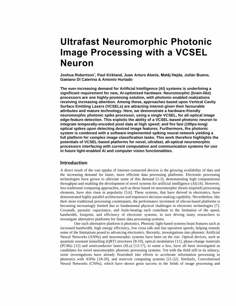
Influence of Source Image Noise. The performance of the edge-feature detecting VCSEL
neuron system is next tested with ‘noisy’ images, see Fig. 4. Noise is implemented into the “Digit 4”
source image via percentage variations of global pixel intensity. The same 8 2x2 kernel operators as in
Figs. 2 and 3, are sequentially applied to the input image, to perform edge detection in a single
experimental run. The performance of the system is measured by counting the number of successful
detections. Fig. 4 reveals noise robust operation for the spiking VCSEL neuron system of this work,
including successful operation under increasing levels of global pixel noise.
The results for globally increasing pixel noise are shown in Fig. 4(a)-(b). Initially, when no
noise is added, the system responds revealing all edge-features in the image. Increasing the global noise
to 5% and 10%, does not significantly affect performance, creating just 11% and 20.1% less successful
activations for edge features. Increasing the global noise further to 15% causes the number of detections
to drop overall (52.2% less activations). Finally, increasing image noise to 20% removes almost all
feature detection (76.1% less activations) as now varying pixel intensities fail to match the kernel
operator, creating input bursts incapable of spike activation. These results demonstrate that source image
can be influenced by a global pixel intensity variation of up to 15% before kernel operators (configured
for noiseless images) struggle to identify target features. Additional results, where intensity variations
are introduced to the background of the printed “Digit 4” image are presented in the supplementary
information.
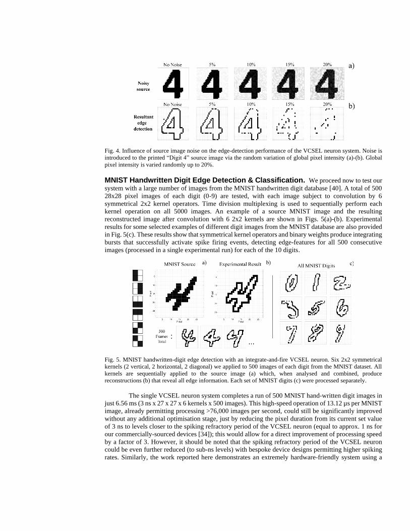
Fig. 4. Influence of source image noise on the edge-detection performance of the VCSEL neuron system. Noise is
introduced to the printed “Digit 4” source image via the random variation of global pixel intensity (a)-(b). Global
pixel intensity is varied randomly up to 20%.
MNIST Handwritten Digit Edge Detection & Classification. We proceed now to test our
system with a large number of images from the MNIST handwritten digit database [40]. A total of 500
28x28 pixel images of each digit (0-9) are tested, with each image subject to convolution by 6
symmetrical 2x2 kernel operators. Time division multiplexing is used to sequentially perform each
kernel operation on all 5000 images. An example of a source MNIST image and the resulting
reconstructed image after convolution with 6 2x2 kernels are shown in Figs. 5(a)-(b). Experimental
results for some selected examples of different digit images from the MNIST database are also provided
in Fig. 5(c). These results show that symmetrical kernel operators and binary weights produce integrating
bursts that successfully activate spike firing events, detecting edge-features for all 500 consecutive
images (processed in a single experimental run) for each of the 10 digits.
Fig. 5. MNIST handwritten-digit edge detection with an integrate-and-fire VCSEL neuron. Six 2x2 symmetrical
kernels (2 vertical, 2 horizontal, 2 diagonal) we applied to 500 images of each digit from the MNIST dataset. All
kernels are sequentially applied to the source image (a) which, when analysed and combined, produce
reconstructions (b) that reveal all edge information. Each set of MNIST digits (c) were processed separately.
The single VCSEL neuron system completes a run of 500 MNIST hand-written digit images in
just 6.56 ms (3 ns x 27 x 27 x 6 kernels x 500 images). This high-speed operation of 13.12 µs per MNIST
image, already permitting processing >76,000 images per second, could still be significantly improved
without any additional optimisation stage, just by reducing the pixel duration from its current set value
of 3 ns to levels closer to the spiking refractory period of the VCSEL neuron (equal to approx. 1 ns for
our commercially-sourced devices [34]); this would allow for a direct improvement of processing speed
by a factor of 3. However, it should be noted that the spiking refractory period of the VCSEL neuron
could be even further reduced (to sub-ns levels) with bespoke device designs permitting higher spiking
rates. Similarly, the work reported here demonstrates an extremely hardware-friendly system using a
single VCSEL for time-multiplexed convolutional operations, yielding output results in the form of fast
(sub-ns long) spikes directly in the optical domain. We note that network architectures with multiple
VCSEL neurons operating simultaneously would also enable parallel computation, further increasing
the speed of the system at the expense of increasing system’s complexity.
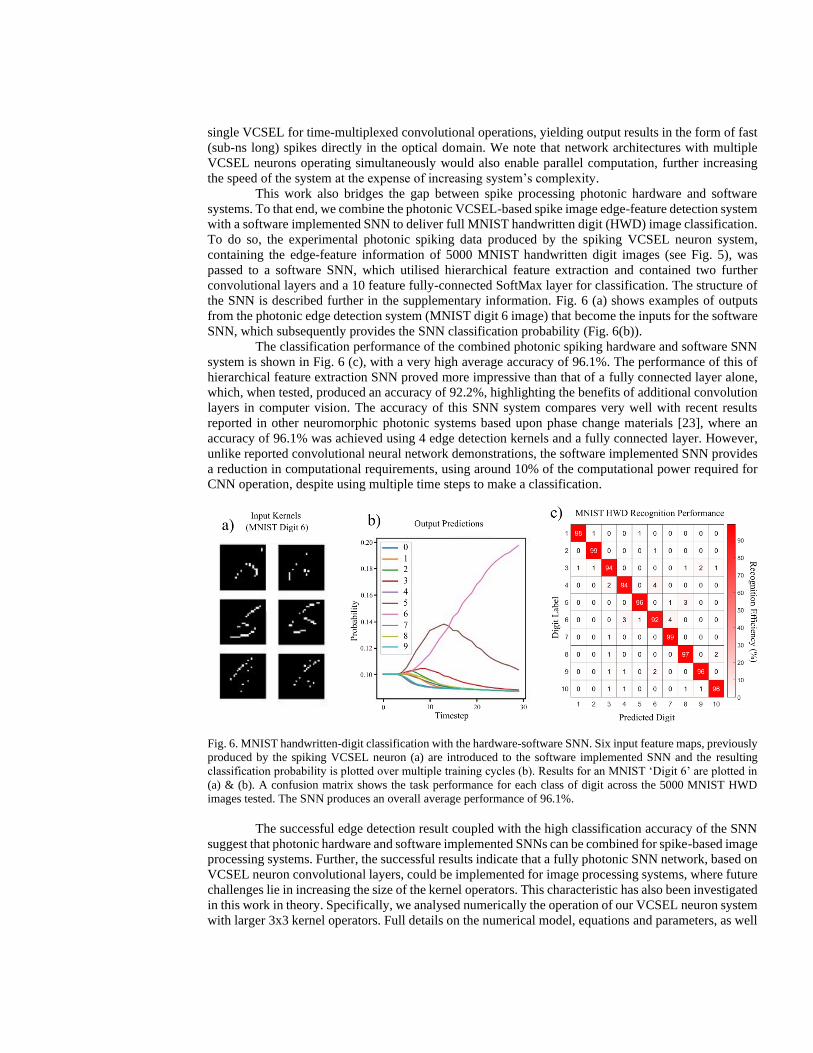
This work also bridges the gap between spike processing photonic hardware and software
systems. To that end, we combine the photonic VCSEL-based spike image edge-feature detection system
with a software implemented SNN to deliver full MNIST handwritten digit (HWD) image classification.
To do so, the experimental photonic spiking data produced by the spiking VCSEL neuron system,
containing the edge-feature information of 5000 MNIST handwritten digit images (see Fig. 5), was
passed to a software SNN, which utilised hierarchical feature extraction and contained two further
convolutional layers and a 10 feature fully-connected SoftMax layer for classification. The structure of
the SNN is described further in the supplementary information. Fig. 6 (a) shows examples of outputs
from the photonic edge detection system (MNIST digit 6 image) that become the inputs for the software
SNN, which subsequently provides the SNN classification probability (Fig. 6(b)).
The classification performance of the combined photonic spiking hardware and software SNN
system is shown in Fig. 6 (c), with a very high average accuracy of 96.1%. The performance of this of
hierarchical feature extraction SNN proved more impressive than that of a fully connected layer alone,
which, when tested, produced an accuracy of 92.2%, highlighting the benefits of additional convolution
layers in computer vision. The accuracy of this SNN system compares very well with recent results
reported in other neuromorphic photonic systems based upon phase change materials [23], where an
accuracy of 96.1% was achieved using 4 edge detection kernels and a fully connected layer. However,
unlike reported convolutional neural network demonstrations, the software implemented SNN provides
a reduction in computational requirements, using around 10% of the computational power required for
CNN operation, despite using multiple time steps to make a classification.
Fig. 6. MNIST handwritten-digit classification with the hardware-software SNN. Six input feature maps, previously
produced by the spiking VCSEL neuron (a) are introduced to the software implemented SNN and the resulting
classification probability is plotted over multiple training cycles (b). Results for an MNIST ‘Digit 6’ are plotted in
(a) & (b). A confusion matrix shows the task performance for each class of digit across the 5000 MNIST HWD
images tested. The SNN produces an overall average performance of 96.1%.
The successful edge detection result coupled with the high classification accuracy of the SNN
suggest that photonic hardware and software implemented SNNs can be combined for spike-based image
processing systems. Further, the successful results indicate that a fully photonic SNN network, based on
VCSEL neuron convolutional layers, could be implemented for image processing systems, where future
challenges lie in increasing the size of the kernel operators. This characteristic has also been investigated
in this work in theory. Specifically, we analysed numerically the operation of our VCSEL neuron system
with larger 3x3 kernel operators. Full details on the numerical model, equations and parameters, as well
as all numerically calculated results, are provided in Supplementary Information. Our theoretical
investigations showed the successful detection of target image features, as well as full edge-feature
detection for larger 3x3 kernel operators. This demonstrates that the VCSEL neuron can successfully
integrate larger bursts of input pulses (9 for the case of 3x3 kernel operators) with ultrashort temporal
durations and separations between consecutive pulses (within the fast integration time-window of the
device), that go beyond the capabilities of our experimental setup. The numerical findings therefore
show that it could be possible to implement multiple layers of VCSEL neurons, such as those currently
implemented by the software in this work (Fig. 6), towards the realisation of future VCSEL-based spike-
based photonic image processing platforms.
Discussion
We demonstrate a neuromorphic photonic system for image processing using a single VCSEL as an
artificial spiking neuron. The system benefits from high speed operation (using 100ps-long inputs) and
hardware-friendly implementation, relying on just a single VCSEL device and time division
multiplexing. The proposed technique utilises the temporal input integration, thresholding, and spike
firing capabilities of the VCSEL neuron, to perform all-optical spiking convolution on complex source
images with a variety of kernel operators. This capability is used to demonstrate all-optical neuromorphic
image edge-feature detection with a VCSEL neuron. Using streams of optical input pulses, we showed
that consecutive 2x2 kernel operators and images can be run with a hardware-friendly single VCSEL
platform, outputting fast neuromorphic spiking events for the detection of target edge features.
Moreover, our approach showed very good robustness to image noise. We demonstrated that the system
can successfully process 5000 images from the benchmark MNIST handwritten digit database. We
showed that 500 images (per digit) can be processed in a single experimental run within 6.56 ms (at
13.12 μs per image) using commercial devices and components at telecom wavelengths, without any
specific VCSEL optimisation stages. Additionally, combining the experimental photonic spiking outputs
from the VCSEL neuron with a software-implemented SNN, we achieved a mean image classification
accuracy of 96.1%, highlighting the potential of our approach for high-speed, low-energy spike-based
image processing. Finally, we demonstrated theoretically that the operation of the VCSEL neuron with
larger dimension (e.g. 3x3) kernels for more complex image feature extraction functionalities is also
possible. This implies that VCSEL neurons have the potential to implement further convolution tasks,
whether it be SNN layers (such as those in our software implemented SNN) or in recognition systems
that target specific features. Overall, we believe that artificial spiking VCSEL neurons show high
potential for future high speed, low energy, and hardware friendly neuromorphic photonic platforms for
image processing with a fast telecom-compatible spiking representation.
Methods
Experimental Setup. The fibre-based optical injection setup used for image processing (edge-
feature detection) with an artificial optical spiking VCSEL is shown in Fig. 1. Light from a tuneable
laser source (TL) is passed through an optical isolator to prevent reflections before entering a variable
optical attenuator (VOA) to control optical injection power. A polarisation controller (PC) is used to
maximize the performance of the 10 GHz Mach Zehnder intensity modulator (MZ), responsible for the
optical encoding of the image input. Image inputs are generated by a 12 GSa/s, 5 GHz arbitrary
waveform generator (AWG, Keysight M8190a) and amplified using an electrical amplifier before being
fed into the MZ modulator. A second PC is then used to set the final polarisation of the optical injection.
A coupler is used to monitor the optical injection power via a power meter (PM), and an optical circulator
is used to inject the signal into the VCSEL neuron. Temporal analysis of the VCSEL neuron’s output is
performed using a 9 GHz photodetector (PD - Thorlabs PDA8GS) and an 8 GHz, 20 GSa/s real-time
oscilloscope (OSC - Rohde & Schwarz RTP). In this work the VCSEL is driven with a bias current of
4.0 mA (Ith = 0.83 mA) and is temperature stabilized at 293 K. The VCSEL device exhibited single
transverse mode lasing with two orthogonal polarisation modes (device characterisation provided in
supplementary information). Injection polarization was matched to that of the dominant (parallel) mode
of the device and was made with a negative frequency detuning from the peak, inducing injection
locking. The encoded inputs were configured to produce short (100ps-long) drops or raises around the
mean optical power of the injected signal (145 µW). When injected input pulses integrate sufficiently,
the injection power drops below the locking threshold, inducing a locking/unlocking transition into a
dynamical regime of excitable spiking dynamics. This mechanism is responsible for the neuronal
functionality of the VCSEL neuron, allowing it to trigger fast sub-nanosecond (approx. 100ps-long)
spiking events in response to target edge features, directly in the optical domain.
Image Edge Detection. Image edge detection is performed according to Fig. 1. The pixel
intensities of the source images are converted into integers (‘1’ for black and ‘-1’ for white). This is
achieved either by averaging across RGB colour channels, or by selecting a specific colour channel,
converting it to greyscale and using a configurable pixel intensity threshold to binarize the pixels
intensities. During the convolution process, kernel operators apply weights to customizable regions of
the source image, producing Hadamard products. The local pattern descriptor identifies the region of the
source image that requires sampling for kernel operation. In this work, the local pattern descriptor is a
square M x N pixel area (highlighted in red in Fig. 1 (c)) with the anchor pixel present at M=N=1. The
local pattern descriptor has a (M+1) x (N+1) range of 2x2 pixels. No image padding was used during
convolution, hence the final dimensions of the convolved image were reduced by 1. In this work, we
demonstrate the in-system integration of multiple data inputs by the VCSEL neuron, thus performing
the pooling of the Hadamard product. To achieve this, we encode the weighted pixel values into a (return-
to-zero) RZ signal, where each value is assigned an individual pulse. Each encoded input pulse has an
amplitude corresponding to its Hadamard product value, and a duration of ~100 ps FWHM. A peak-to-
peak separation of ~150 ps is used between input pulses, with zero padding also added to fill the pixel
to a configurable window. In this work a pixel window of 3.0 ns was selected, higher than the refractory
period of the spiking dynamics in the VCSEL neuron (approx. 1 ns long), allowing each pixel to
independently activate spiking responses. This encoding scheme makes use of time-division
multiplexing to encode the Hadamard product into a sequence of input pulses and encode multiple
convolution operations sequentially into a single device. The activation threshold, governed by the
injection power and frequency detuning, is required to be set such that only inputs burst associated with
image target features trigger activations.
Influence of Noise on Edge Detection Performance. To implement global noise all pixel
intensity was varied randomly according to the configurable noise percentage (%). The source image
was implemented with 0%, 5%, 10%, 15% and 20% global noise. The weights of the kernel operators
had to be altered such that the activation threshold was consistent for all integrating bursts across the 8
kernel operations. The maximum integrated input was therefore normalized by adjusting the vertical and
horizontal kernel weights to the non-integer value of 0.75, such that 0.75+0.75+0.75+0.75 = 3. Finally,
the convolutions of all 5 noisy images were combined into a single image input, such that the activation
threshold was consistent across all tested images.
Data availability
All data underpinning this publication are openly available from the University of Strathclyde
KnowledgeBase at https://doi.org/10.15129/cfc1e947-9afe-40fd-bb4b-c7e271a77941.
References
1. Krizhevsky, A., Sutskever, I. & Hinton, G. E. ImageNet classification with deep convolutional neural networks. In Advances
in Neural Information Processing Systems 25 (eds Bartlett, P. et al.) 1097–1105 (Curran Associates, 2013). 2. Wang, P. S. et al. O-CNN: octree-based convolutional neural networks for 3D shape analysis, ACM Trans. Graph. 36(4),
(2017).
3. Zhang, C. et al. Optimizing FPGA-based accelerator design for deep convolutional neural networks. In Proc. 2015 ACM/SIGDA International Symposium on Field-programmable Gate Arrays 161–170 (Association for Computing
Machinery, 2015)

4. LeCun, Y., Bengio, Y. & Hinton, G. Deep learning. Nature 521, 436–444 (2015).
5. DeBole, M. V. et al. TrueNorth: accelerating from zero to 64 million neurons in 10 years. Computer 52, 20–29 (2019).
6. Friedmann, S. et al. Demonstrating Hybrid Learning in a Flexible Neuromorphic Hardware System. IEEE Trans. Biomed. Circuits Syst. 11, 128–42 (2017).
7. Miller, D. A. B. Attojoule optoelectronics for low-energy information processing and communications. J. Lightwave
Technol. 35, 346–396 (2017). 8. Romeira, B., Figueiredo, J.L. & Javaloyes, J. NanoLEDs for energy-efficient and gigahertz-speed spike-based sub-λ
neuromorphic nanophotonic computing. Nanophotonics, 9(13), 4149-4162 (2020).
9. Ortega-Piwonka, I. et al. Bursting and excitability in neuromorphic resonant tunnelling diodes. J. Phys. Rev. Applied, 15, 034017 (2021).
10. Romeira, B. et al. Excitability and Optical Pulse Generation in Semiconductor Lasers Driven by Resonant Tunnelling Diode
Photo-detectors. Opt. Exp. 21, 20931 (2013). 11. George, J. K. et al. Neuromorphic Photonics with Electro-absorption Modulators. Opt. Exp. 27, 5181 (2019).
12. Feldmann, J. et al. All-optical Spiking Neurosynaptic Networks with Self-learning Capabilities. Nature, 569, 208–215 (2019).
13. Pammi, V. A. et al. Photonic Computing with Single and Coupled Spiking Micropillar Lasers. IEEE J. Sel. Top. Quantum
Electron. 26, 1–7 (2020). 14. Selmi, F. et al. Spike Latency and Response Properties of an Excitable Micropillar Laser. Phys. Rev. E, 94, 042219 (2016).
15. Dillane, M. et al. Excitable Interplay Between Lasing Quantum Dot States. Phys. Rev. E. 100, 012202 (2019).
16. Dillane, M. et al. Asymmetric excitable phase triggering in an optically injected semiconductor laser. Opt. Lett. 46, 440-443 (2021).
17. Sarantoglou, G., Skontranis M. & Mesaritakis C. All Optical Integrate and Fire Neuromorphic Node Based on Single Section
Quantum Dot Laser. IEEE J. Sel. Top. Quantum. Electron. 26(5), 1-10 (2020). 18. Tait, A. N. et al. Neuromorphic photonic networks using silicon photonic weight banks. Sci. Rep. 7(1), 7430 (2017).
19. Shainline, J. M. et al. Superconducting optoelectronic circuits for neuromorphic computing. Phys. Rev. Appl. 7, 034013
(2017). 20. Tait, A. N. et al. Broadcast and weight: An integrated network for scalable photonic spike processing. J. Lightw. Technol.,
32(21), 4029–4041 (2014).
21. Antonik, P. et al. Human action recognition with a large-scale brain-inspired photonic computer. Nat. Mach. Intell. 1(11), 530–537 (2019).
22. Bueno, J. et al. Conditions for reservoir computing performance using semiconductor lasers with delayed optical feedback.
Opt. Express, 25(3), 2401–2412 (2017). 23. Feldmann, J. et al. Parallel convolutional processing using an integrated photonic tensor core. Nature, 589, 52–58 (2021).
24. Mehrabian, A. et al. PCNNA: a photonic convolutional neural network accelerator. in IEEE International System-on-Chip
Conference (SOCC) (2018), 169–173 (2018). 25. Xu, S. et al. High-accuracy optical convolution unit architecture for convolutional neural networks by cascaded acousto-
optical modulator arrays. Opt. Exp., 27, 19778–19787 (2019).
26. Prucnal, P. R., Shastri, B. J. & Ferreira de Lima, T. Recent Progress in Semiconductor Excitable Lasers for Photonic Spike Processing. Adv. Opt. Photon. 8, 228–299 (2016).
27. Kirkland, P. et al. SpikeSEG: Spiking segmentation via STDP saliency mapping. In 2020 International Joint Conference on
Neural Networks (IJCNN), 1-8, (2020). 28. Kirkland, P. et al. UAV Detection: A STDP Trained Deep Convolutional Spiking Neural Network Retina-Neuromorphic
Approach. In Artificial Neural Networks and Machine Learning – ICANN 2019: Theoretical Neural Computation. ICANN
2019., Lecture Notes in Computer Science, vol 11727. Springer, Cham., (2019). 29. Kirkland, P. et al. Imaging from temporal data via spiking convolutional neural networks. In Proc. SPIE 11540, Emerging
Imaging and Sensing Technologies for Security and Defence V; and Advanced Manufacturing Technologies for Micro- and
Nanosystems in Security and Defence III, 115400J, (2020). 30. Park, J. et al, A 65k neuron 73-Mevents/s 22-pJ/event asynchronous micro-pipelined integrate and-fire array transceiver. In
IEEE 2014 Biomedical Circuits and Systems Conference, BioCAS 2014–Proceedings, pp. 675–678, (2014).
31. Song, Z. et al. Photonic spiking neural network based on excitable VCSELs-SA for sound azimuth detection. Opt. Express 28, 1561-1573 (2020).
32. Robertson, J. et al. Toward neuromorphic photonic networks of ultrafast spiking laser neurons. IEEE J. Sel. Top. Quantum
Electron. 26, 7700715 (2019).
33. Deng, T., Robertson, J. & Hurtado, A. Controlled propagation of spiking dynamics in vertical-cavity surface-emitting lasers:
towards neuromorphic photonic networks. IEEE J. Sel. Top. Quantum Electron. 23, 1800408 (2017).
34. Hejda, M. et al. Spike-based information encoding in VCSELs for neuromorphic photonic systems. J. Phys. 2, 044001 (2020).
35. Robertson, J. et al. Ultrafast optical integration and pattern classification for neuromorphic photonics based on spiking
VCSEL neurons. Sci. Rep. 10, 1 (2020). 36. Xiang, S. et al. STDP-based unsupervised spike pattern learning in a photonic spiking neural network with VCSELs and
VCSOAs. IEEE J. Sel. Top. Quantum Electron. 25, 1700109 (2019).
37. Robertson, J. et al. Image edge detection with a photonic spiking VCSEL-neuron. Opt. Exp. 28, 37526-37537 (2020). 38. Zhang, Y. et al. All-optical neuromorphic binary convolution with a spiking VCSEL neuron for image gradient magnitudes.
Photon. Res. 9, B201-B209 (2021).

39. Hejda, M. et al. Neuromorphic encoding of image pixel data into rate-encoded optical spike trains with a photonic VCSEL-
neuron. Appl. Phys. Lett. Photon. 6, 060802 (2021).
40. LeCun, Y. THE MNIST DATABASE of handwritten digits. Courant Institute, NYU Corinna Cortes, Google Labs, New York, Microsoft Research, Redmond.
Acknowledgments
The authors acknowledge support from the UKRI Turing AI Acceleration Fellowships Programme
(EP/V025198/1), the US Office of Naval Research Global (Grant ONRG-NICOP-N62909-18-1-2027),
the European Commission (Grant 828841-ChipAI-H2020-FETOPEN-2018-2020), the EPSRC Doctoral
Training Partnership (EP/N509760), and Leonardo MW Ltd through the Leonardo Lectureship at
Strathclyde.
Author contributions
J.R, M.H, J.A.A, & J.B carried out the experimental work under the supervision of A.H. P.K obtained
classification results with the software SNN under the supervision of G.D. All authors helped identify
the presented work, discussed the results, and contributed to the writing of the manuscript.
Competing interests
The authors declare no competing interests.

Ultrafast Neuromorphic Photonic
Image Processing with a VCSEL
Neuron
Joshua Robertson*, Paul Kirkland, Juan Arturo Alanis, Matěj Hejda, Julián
Bueno, Gaetano Di Caterina & Antonio Hurtado
Supplementary Information
Table of Contents
1. Vertical-Cavity Surface Emitting Lasers (VCSEL) Characterisation
2. Image Inputs and Optical Integration
3. Background Noise Variation
4. Spiking Neural Network (SNN) structure
5. Theoretical Analysis of Larger Kernel Operation
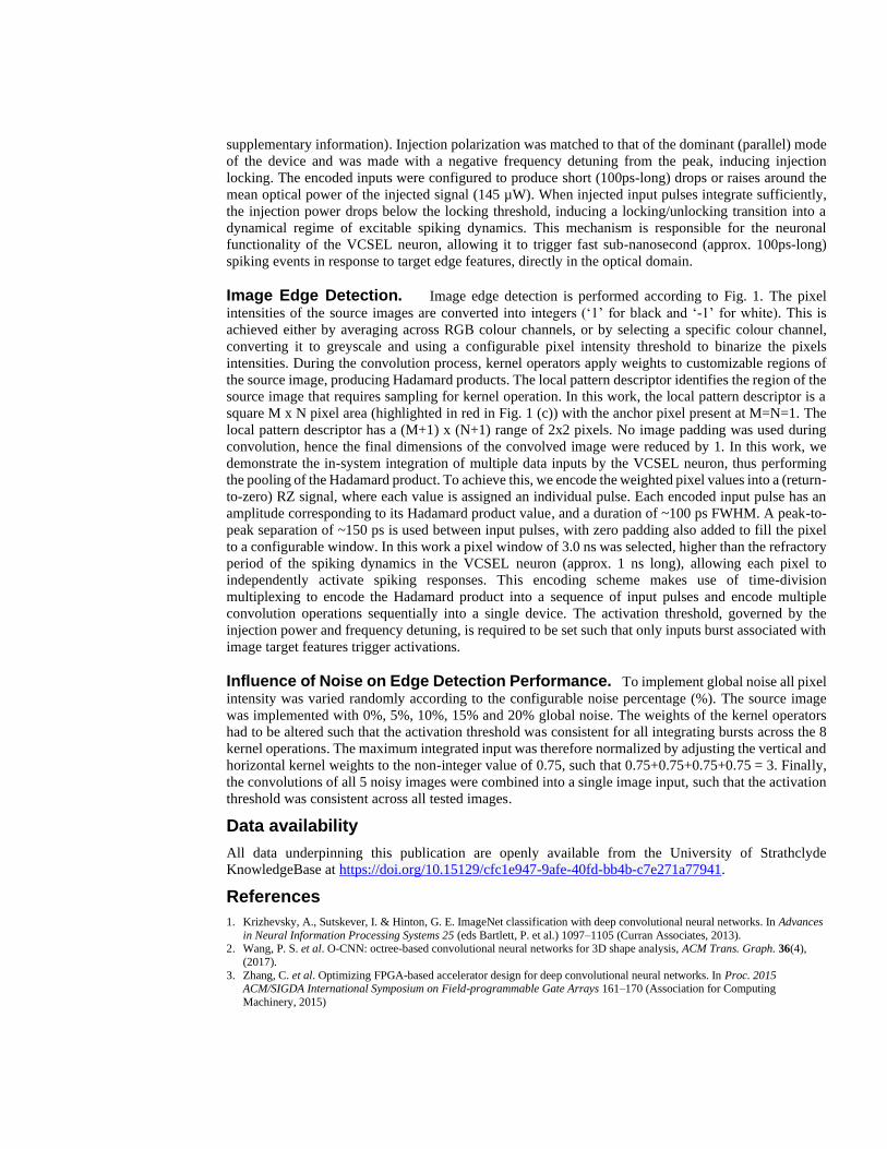
Vertical Cavity Surface Emitting Laser (VCSEL) Characterisation. A single mode
vertical-cavity surface-emitting laser (VCSEL) was used to create a photonic spiking processing
system for image edge-feature detection. The VCSEL used in this work was a commercially
available device operating at the telecom wavelength of 1550 nm. The device was tested and
characterised prior to the operation demonstrated in the manuscript. Fig. S1 plots the VCSEL’s
output power and lasing spectra at different bias currents when temperature stabilised at 293 K. Fig.
S1a plots the L-I curve of the device measured at 293 K, showing a threshold current of I th = 0.83
mA. When biased above threshold the device delivers continuous wave (CW) light emission. Fig.
S1b shows the red shift of lasing spectra with increasing applied bias current. The VCSEL used in
this work was a single-longitudinal and single-transverse mode laser source, which had two
coexisting linear and orthogonally-polarised modes, referred to here as the orthogonally-polarised
(λx) and parallel-polarised (λy) modes. The device operated with a dominant parallel λy mode and
did not exhibit bias-induced polarisation switching across the measured operating parameters. At
4.0 mA the peak wavelength of the dominant λy mode was found at 1286.97 nm and the peak of the
subsidiary λx mode at 1287.11 nm. The corresponding wavelength separation between the two
orthogonally-polarised modes for this device was measured as 0.136 nm (24.7 GHz). In this work
injection of the image data input was made into the parallel λy mode of the device with injection
polarisation matching the dominant mode of the VCSEL.
Fig. S1. Characterisation of the VCSEL. The output power was measured against bias current to determine the
threshold of the device (a). The threshold current was equal to 0.83 mA. The lasing spectra of the device was
recorded for increasing bias currents using an optical spectrum analyser (b). At the operating current of 4.0 mA
the device demonstrated two orthogonal polarisation modes (λy and λx) with peak wavelength of 1286.97 nm
and 1287.11 nm respectively.

Image Inputs and Optical Integration. The photonic VCSEL neuron is responsible for
the integration of optical inputs, the thresholding of their total contribution and the activation of fast
spiking dynamics. Here, as described in Fig. 1 in the main article, image inputs are created by time-
multiplexing the Hadamard product values of convolution operations, forming return-to-zero (RZ)
encoded waveforms with bursts of positive and negative pulses. The RZ waveforms, or image inputs,
are subsequently generated in an arbitrary waveform generator and encoded into the optical intensity
of a tunable laser for injection into the VCSEL neuron. When the encoded injection enters the device,
the inputs are integrated and the VCSEL neuron responds with fast spike events when its threshold
for spike firing is exceeded. In this report the input pulses are generated at a rate of 12 GSa/s (1
sample per input), creating ~100 ps long pulses. The input pulses are grouped into fast ~700 ps
bursts at the beginning of a configurable pixel window (equal to 3 ns in this work). Following the 3
ns window the pulse burst of the next pixel in the convolution process is generated. The generated
image input is encoded into the optical injection entering the VCSEL neuron such that positive
inputs produce negative intensity drops. Fig. S2a shows an example of encoded optical injection.
The optical injection corresponds to the convolution of pixels 14-19 in row 13 of the printed “Digit
4” image with a 2x2 vertical kernel.
Fig. S2. Input-encoded injection and the subsequent VCSEL neuron response. The encoded optical injection,
incident on the VCSEL neuron, is shown for the the convolution of pixels 14-19 in row 13 of the printed “Digit
4” with a 2x2 vertical kernel (a). The VCSEL neuron responds to the incoming signal by firing a spiking event
for a target feature detection (pixel 17) (b).
As expected, the encoded optical injection takes the form of sequential bursts of positive and
negative pulses. When a mismatch between kernel and local pattern descriptor (selected pixels) is
present, combinations of positive and negative pulses occur within the same burst, as in the case of
pixels 15,16,18 and 19 (see Fig. S2a). These inputs, when integrated by the VCSEL neuron, produce
a low energy contribution to the activation threshold, subsequently failing to activate a spiking
response in the recorded VCSEL neuron output shown in Fig. S2b. In contrast, when a kernel
matches the local pattern descriptor, the injection is encoded with 4 negative inputs, as shown in
pixel 17. Once injected into the neuron, the 4 negative inputs combine to produce a change in
injection power that crosses the threshold for spike activation. This subsequently triggers an
excitable spike at the output of the VCSEL neuron, as shown in Fig S2b. Following the successful
or unsuccessful activation of spiking responses the system is reset during the remainder of the 3 ns
window. This approach to input encoding and optical integration is used throughout this work
including each demonstration of edge detection with the VCSEL neuron and the initial photonic
hardware layer of the SNN used for the classification of MNIST hand-written digit (HWD) images.
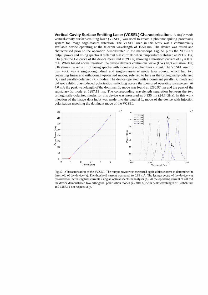
Background Noise Variation. As described in the main article, the edge detection
performance of the system was tested on the printed “Digit 4” image for increasing source image
noise. In addition to testing increasing global pixel noise, we have tested performance on source
images with increasing background noise. To implement background noise in source images the
intensity of each white pixel was varied randomly between its current value (-1) and a percentage
(%) of the maximum intensity value (1). For a background noise of 100% white pixels could vary
randomly between white (-1) and black (1). The source image was implemented with 0%, 20%,
40%, 60% and 80% background noise. Figs. S3(a) and 4(b) analyse the case of increasing
background pixel noise, revealing good overall resilience to noise. Initially, when no noise is added,
the system responded revealing all edge-features in the image. Increasing the background noise to
20% (Figs. 4(a)-(b)), did not dramatically affect performance, decreasing slightly (25.9% reduction)
the number of successful detections (firing of sub-ns spikes). Increasing the background noise to
40% and 60% we observed the number of detections reduced overall (57.7% and 79.8% less
successful activations). Despite this, the image became unrecognisable, and performance further
decreased as background noise reached 80%. These results show that without altering the threshold
of the system, target features can still be recognised up to 40% background noise.
Fig. S3. Influence of source image noise on the edge-detection performance of the VCSEL-Neuron system.
Noise was introduced to the printed “Digit 4” source image via the random variation of background-pixel
intensity (a)-(b), and the random variation of global pixel intensity (c)-(d). Background pixels had their intensity
values randomly varied by up to 80%, global pixel intensity was varied up to 20%.

Spiking Neural Network (SNN) Structure. A software implemented spiking neural
network (SNN) is incorporated alongside a photonic VCSEL neuron spiking edge detection system
to achieve the classification of MNIST handwritten digit images. As described in the main article,
the optical spiking data generated by the experimental VCSEL neuron is fed to the software
implemented SNN. The structure of the complete system is shown in Fig. S4.
Fig. S4. The structure of Spiking Neural Network used in this work in combination with the VCSEL neuron
photonic system for the classification of MNIST images. The first layer of the SNN is the experimental VCSEL
neuron which performs spiking convolution with 2x2 kernel operators, creating a photonic spiking data stream.
The software implemented SNN is fed the experimental data, subsequently performing convolution in 2
additional convolutional layers. The output of the second convolutional layer is flattened and passed to a 10
feature fully connected layer for classification.
The first layer of the SNN system is built experimentally with a single VCSEL neuron. This layer
uses 6 2x2 kernel operators to yield edge-feature detection outputs in the form of fast optical spikes
(as shown in Fig. 5 of the main article). The photonic spiking data is detected (with a >9.5 GHz
bandwidth amplified photodetector) and recorded using a fast real-time oscilloscope. The recorded
spiking time series are then fed into the software-implemented spiking neural network. The software
implemented SNN made use hierarchical feature extraction and hence implemented a further two
convolutional layers. The first SNN convolution layer created 256 feature maps using 5x5 kernel
operators with a stride of 2x2, reducing the dimension of the feature maps to 12x12. The second
convolution layer created 512 feature maps using 3x3 kernel operators again with a stride of 2x2,
further reducing the dimension of the feature maps to 5x5. A flattening layer was used to prepare
the network for the final 10 feature fully connected SoftMax layer which provided output
probabilities for the final classification of the MNIST HWD image. The classification of 5000
MNIST HWD images were tested in this work and the recognition efficiencies are provided in Fig.
6 of the main article.
The network was constructed with the help of the Tensorflow and Keras libraries before
being converted to a leaky integrate and fire system using the Nengo DL libraries. This method
allowed backpropagation through gradient descent to be used to train the network weights prior to
the conversion into a SNN. The completion of the training before SNN conversion also granted the
use of well-established software training tools. In this work multiple training time steps were used
before the final performance of the network was measured, as demonstrated in Fig. 6 of the main
article. Overall, the method of converting a CNN to a SNN helped simplify implementation and
training but did however influence the performance of the system. The average performance of the
MNIST HWD classification reduced from 97.9% to 96.1% following the conversion to an SNN.
This drop is performance is a trade off with the improvement to computational requirements, with
the SNN using around 10% of that required by the CNN.

Theoretical Analysis of Larger Kernel Operation. To investigate further the potential
of the neuromorphic image processing system of this work, convolution with larger (3x3) kernel
operators was simulated using the Spin-Flip Model (SFM). The SFM equations (SI 1-5) were
modified to include additional optical injection terms and were solved using the fourth order Runge-
Kutta method:
( ) ( )
( )( ) ( )
,
, ,
, , ,1 x
x y
a x y p x y
i t
x y x y inj inj x y
dEk E i k E
dt
k i NE inE k E t e F
= − −
+ + + +
(SI 1)
( ) ( )22 * *1N x y y x x y
dNN E E in E E E E
dt = − + + − + −
(SI 2)
( ) ( )22 * *
s N x y y x x y
dnn n E E iN E E E E
dt = − − − + −
(SI 3)
( )1 22
sp N
xF N n N n
= − + + − (SI 4)
( )1 22
sp N
yF i N n N n
= − + + − (SI 5)
In equations S1 1-5, subscripts x and y represent the subsidiary (orthogonally-polarised) and solitary
(parallel-polarised) lasing modes of the VCSEL respectively. The field amplitudes of the subsidiary
and solitary modes are represented by Ex and Ey. The total carrier inversion between conduction and
valence bands is represented by N, with n representing the carrier inversion difference between spins
of opposite polarity. γa is the gain anisotropy (dichroism) rate, γp is the linear birefringence rate, γN
is the decay rate of the carrier inversion and γs is the spin-flip rate. k is the field decay rate, α is the
linewidth enhancement rate and μ is the normalized pump current (where μ= 1 represents the
VCSEL’s lasing threshold value). The injected image input, using here larger 3x3 kernel operators,
is represented by Einj and the injection strength is controlled by kinj. The spontaneous emission noise
Fx and Fy are calculated using the spontaneous emission strength βsp and two independent Gaussian
white noise terms, ξ1,2, of zero mean and a unit variance. The angular frequency detuning is defined
as Δωx = ωinj-ω0, where the central frequency ω0 = (ωx+ωy)/2 lies between the frequencies of the
subsidiary ωx = ω0+αγa-γp and the solitary mode ωy = ω0+γp-αγa. Δf = finj-fx is the frequency detuning
between the injected field and the subsidiary mode, hence Δωx = 2πΔf+αγa-γp. The following
parameters were used to simulate the response of a VCSEL neuron: γp =128 ns-1, γa =2 ns-1, γN =0.5
ns-1, γs =110 ns-1, α =2, k =185 ns-1, kinj =15 ns-1 and βsp =10-5. Einj was introduced into the x
polarisation mode with a frequency detuning of Δf = -4 GHz.
Here, image inputs were generated using the same technique as that shown in Fig.1 of the
main article. Each image input implements bursts of 9 input pulses (using a 3x3 kernel), one for
each Hadamard product value. The input pulses were configured with pulse widths of 100 ps and
with short pulse separations of 10 ps (to fit within the temporal integration window of the VCSEL
neuron, equal to ~1 ns), within a configurable 3 ns pixel duration. As before, the simulated VCSEL
is responsible for the integration of inputs and the activation of spiking responses for target features.
The successful integration of a 9-burst input, and the activation of a fast spiking response, is shown
in the numerically calculated result of Fig. S5. Here a burst of 9 inputs, is injected into the device
producing the desired spiking response from the VCSEL, hence the integration of large input bursts
can be theoretically performed.
Using an image from the MNIST handwritten digit database (Fig. S6 (a)), convolution with
8 3x3 kernel operators was numerically simulated (Fig. S6 (c)-(j)). The 8 3x3 kernel operators
implemented integer weights, 1 for black and -1 for white, as shown at the bottom of Fig. S6. The
results showed that each kernel operator successfully detected the target features within the MNIST
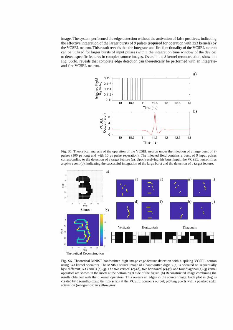
image. The system performed the edge detection without the activation of false positives, indicating
the effective integration of the larger bursts of 9 pulses (required for operation with 3x3 kernels) by
the VCSEL neuron. This result reveals that the integrate-and-fire functionality of the VCSEL neuron
can be utilized for larger bursts of input pulses (within the integration time window of the device)
to detect specific features in complex source images. Overall, the 8 kernel reconstruction, shown in
Fig. S6(b), reveals that complete edge detection can theoretically be performed with an integrate-
and-fire VCSEL neuron.
Fig. S5. Theoretical analysis of the operation of the VCSEL neuron under the injection of a large burst of 9-
pulses (100 ps long and with 10 ps pulse separation). The injected field contains a burst of 9 input pulses
corresponding to the detection of a target feature (a). Upon receiving this burst input, the VCSEL neuron fires
a spike event (b), indicating the successful integration of the large burst and the detection of a target feature.
Fig. S6. Theoretical MNIST handwritten digit image edge-feature detection with a spiking VCSEL neuron
using 3x3 kernel operators. The MNIST source image of a handwritten digit 3 (a) is operated on sequentially
by 8 different 3x3 kernels (c)-(j). The two vertical (c)-(d), two horizontal (e)-(f), and four diagonal (g)-(j) kernel
operators are shown in the insets at the bottom right side of the figure. (b) Reconstructed image combining the
results obtained with the 8 kernel operators. This reveals all edges in the source image. Each plot in (b-j) is
created by de-multiplexing the timeseries at the VCSEL neuron’s output, plotting pixels with a positive spike
activation (recognition) in yellow/grey.