Embed Size (px)
Citation preview
SURFACE AND INTERFACE ANALYSISSurf. Interface Anal. 27, 533È536 (1999)
Ultrahigh Vacuum Scanning TunnellingMicroscopy Studies of the Decapped InAsQuantum Dots on GaAs(001) Surface afterDesorption of a Protective As Layer
L. N. Bolotov,1 A. Nakamura,2 V. P. Evtikhiev,1 V. E. Tokranov1 and A. N. Titkov1,*1 A. F. Io†e Institute, 26 Polytekhnicheskaya, 194021 St. Petersburg, Russia2 CIRSE, Nagoya University, Chikusa-ku, Nagoya 464-01, Japan
The morphology and electronic properties of InAs quantum dots (QDs) on the GaAs(001) surface has been studiedby ultrahigh vacuum scanning tunnelling microscopy/spectroscopy after removal of a preliminary deposited protec-tive As layer. A thermal annealing procedure has been developed, which, applied to a sample with an As cap layer,allows InAs QDs to be opened on the surface of an InAs wetting layer (WL) exhibiting a [2 Â 4 ] reconstruction ofAs dimers. Scanning tunnelling spectroscopy measurements on the decapped surface show that I–V characteristicstaken with the microscope tip positioned over single InAs QDs have a smaller voltage width for zero conductivity(dI/dV = 0) when compared with those taken over the InAs WL, which are essential the same as the I–V character-istics for a clean GaAs surface. This observation seems to indicate a weakening of the surface band bending in theareas beneath InAs QDs. Copyright 1999 John Wiley & Sons, Ltd.(
KEYWORDS: UHV STM; InAs quantum dots ; As decapping
INTRODUCTION
Self-assembled IIIÈV semiconductor quantum dots(QDs) are interesting objects of modern semiconductorphysics with regard to both fundamental research andnovel applications. O†ering a genuine three-dimensional carrier conÐnement, QD ensembles possessunique optical and electronic properties being of partic-ular interest for the development of light-emitting andother electronic devices of the next generation.1h4 Togain better insight into the properties of QDs, directstudies of open single QDs in ultrahigh vacuum (UHV)are certainly necessary. In some experiments, sampleswith QDs on their surface must be transferred throughthe atmosphere before being inserted into the UHVchamber, so proper protection of the sample surfaceagainst oxidation and contamination is necessary. Thisgoal can be achieved by capping the surface with a pro-tective layer that can be desorbed later in the UHV.
In this work we studied the possibility of using anamorphous As capping layer to protect InAs QDs onthe GaAs(001) surface. For the GaAs(001) surface, pro-tection with the As capping layer is well known.5h8However, in order to obtain a clean GaAs surface witha clearly resolved [2] 4] reconstruction of As dimers,it is necessary to heat samples to 450 ¡C.6,8 In the caseof InAs QDs on the GaAs(001) surface, these heating
* Correspondence to : A. N. Titkov, A. F. Io†e Institute, 26 Poly-tekhnicheskay 194021 St Petersburg, Russia.
E-mail : titkov=agvb.io†e.rssi.ru
temperatures may be too high because of possible InAsdesorption from the GaAs substrate.9,10 In this connec-tion, we attempted to remove the As capping layer fromInAs QDs at lower temperatures. The decapped sur-faces were studied in the UHV by scanning tunnellingmicroscopy and spectroscopy (STM/S). Finally, we wereable to perform local spectroscopic studies of decappedsingle InAs QDs.
EXPERIMENTAL
The InAs QDs studied were molecular beam epitaxy(MBE) grown on a GaAs(001) surface by the followingprocedure. After desorption of the native oxide from anon-axis GaAs(001) semi-insulating wafer, a 400 nm thickp-type (B\ 1017 cm~3) GaAs bu†er layer was grown at600 ¡C. A reÑection high-energy electron di†raction(RHEED) pattern taken at the end of bu†er growthshowed a streaky [2 ] 4] reconstruction of As dimers.For subsequent growth of InAs QDs, the substrate tem-perature was lowered to 490 ¡C and two monolayers ofInAs were deposited at a growth rate of 0.15 ML s~1.The equivalent pressure of the beam was 4] 10~6As2Torr and the V/III ratio was 10. After completion ofInAs deposition, the samples were cooled rapidly toroom temperature (RT) and capped with a 500 nm thickAs layer deposited using an cracker cell.As2After storage in air, the samples were mounted on theSTM sample holder and introduced into the storagechamber of a JEOL 4650 UHV scanning tunnelling
CCC 0142È2421/99/050533È04 $17.50 Received 15 September 1998Copyright ( 1999 John Wiley & Sons, Ltd. Accepted 8 December 1998
534 L. N. BOLOTOV ET AL .
microscope (base pressure 7 ] 10~11 Torr). The Aslayer was desorbed on the STM sample holderequipped with a ceramic heater. The ceramic heater wascalibrated in a special experiment in which the rate ofAs desorption from the GaAs wafer was monitored.Previously, it has been found5 that the As layer isdesorbed in two steps. With increasing temperature, therate of As desorption Ðrst shows a weak peak at 160 ¡C,followed by a stronger one at 350 ¡C. To determinethese speciÐc temperatures, we heated the GaAssamples by very slowly increasing the heating current.The rate of As desorption was monitored by the rate ofpressure build-up in the storage STM chamber. Thesetwo temperature points permitted us to Ðt the heatercalibration curve supplied by the JEOL Company forthe case of Si sample heating.
Prior to decapping, the sample surfaces weredegassed at 300 ¡C for several hours, with the pressuremaintained close to 10~9 Torr. Further sample heatingwas performed on the STM stage in the measuringSTM chamber (base pressure 5 ] 10~11 Torr). Samplescould be heated up to 600 ¡C. To perform STM mea-surements, samples were cooled to RT.
The STM images were taken using a tungsten tip inconstant current mode with a negative sample bias inthe range from [2.5 to [4.0 V and tunnel currents of0.1È0.5 nA. Local IÈV characteristics were measured forthe decapped InAs QDs and the Ñat surface terracesbetween them.
RESULTS AND DISCUSSION
We started removal of the As layer form InAs QDs onthe GaAs(001) surface at 320È330 ¡C. It was found thatprolonged heating at this temperature (for 4 h in ourcase) can remove most of the As layer and even revealthe InAs QDs, as can be seen in the STM image in Fig.1(a). However, the InAs QDs and the surface betweenthem remain covered by several monolayers of the Ascap [see also Fig. 1(b), which presents the proÐle takenover the STM image along the white line in Fig. 1(a)],and even longer heating at these temperatures cannotproduce a clean surface. It is worth mentioning that therest of the As cap layers do not show any dimer struc-ture.
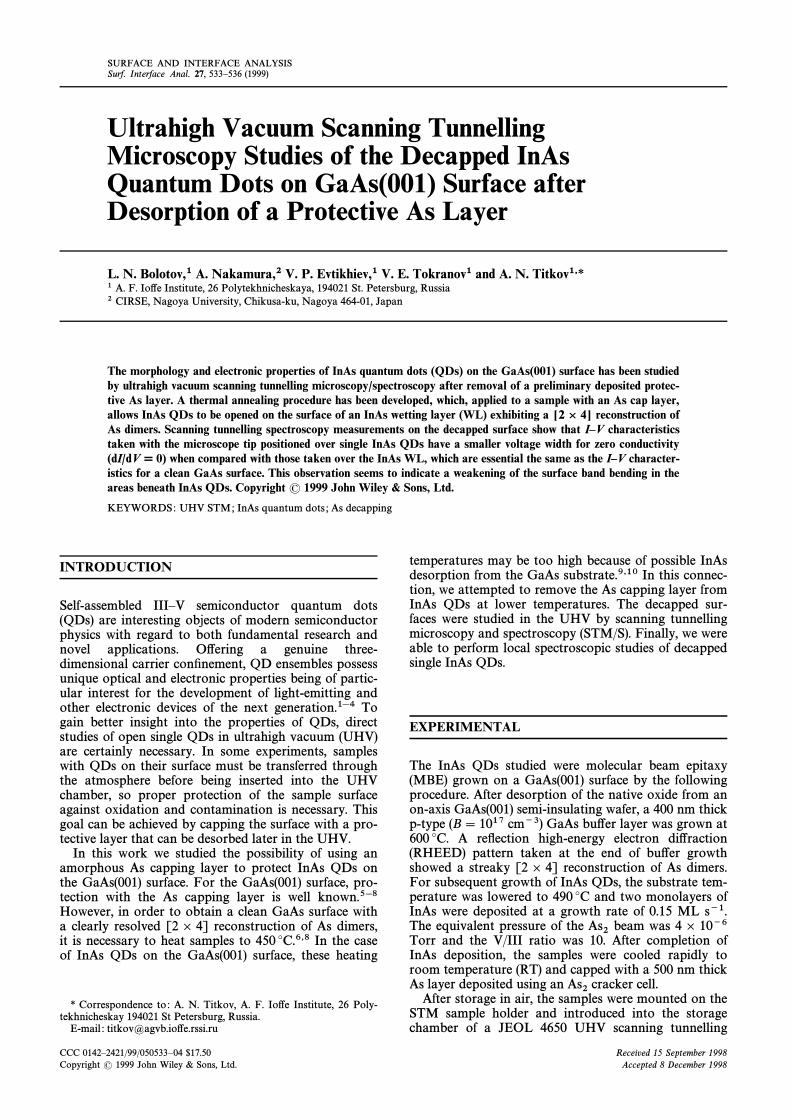
We succeeded in obtaining clean surface only afteradditional heating at 360È370 ¡C (for 15 min). The STMimage in Fig. 2(a) shows the well-pronounced InAs QDson a clean surface with As dimer rows along the[[110] direction. The STM image proÐles taken overQDs [Fig. 2(b)] indicate that the InAs QDs havedimensions typically obtained under the chosen MBEgrowth conditions : averaged base diameter of 14 nmand aspect ratio of 0.18.4,11 The As dimer rows runfrom the upper-left to the lower-right of the image.These rows are better resolved in the enlarged STMimage of the surface area without InAs QDs, shown inthe inset in Fig. 2(a). The dimer rows are separated inparts and exhibit many kinks, which is typical for theAs dimer rows.7,9
The STM data in Fig. 2 also show that the surfacebetween the InAs QDs is characterized by only twoheight levels separated by a step of single bilayer height
Figure 1. (a) A UHV STM image of InAs QDs on a GaAs(001)surface covered by several monolayers of an As capping layer. (b)Profile taken over the STM image (a).
(2.8 It is interesting to note that the higher level isÓ).represented by atomically Ñat terraces covering approx-imately half of the whole surface. It is worth mentioningthat the formation of the InAs QDs on a GaAs surfacestarts only after preliminary growth on the same surfaceof a two-dimensional InAs wetting layer (WL) ofaverage thickness 1.5 ML.1,4 Thus, we believe that wehave also successfully decapped the InAs WL. In thiscase it follows from our STM data that the InAs QDspreferentially grow on the upper InAs terraces.
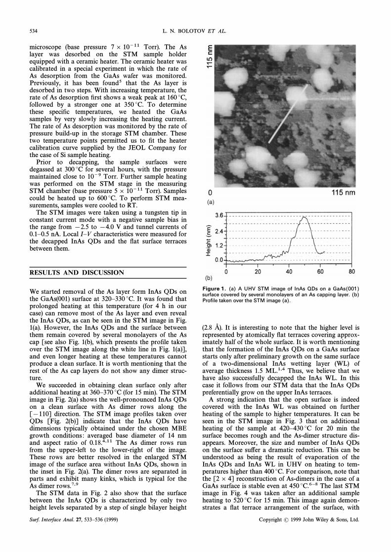
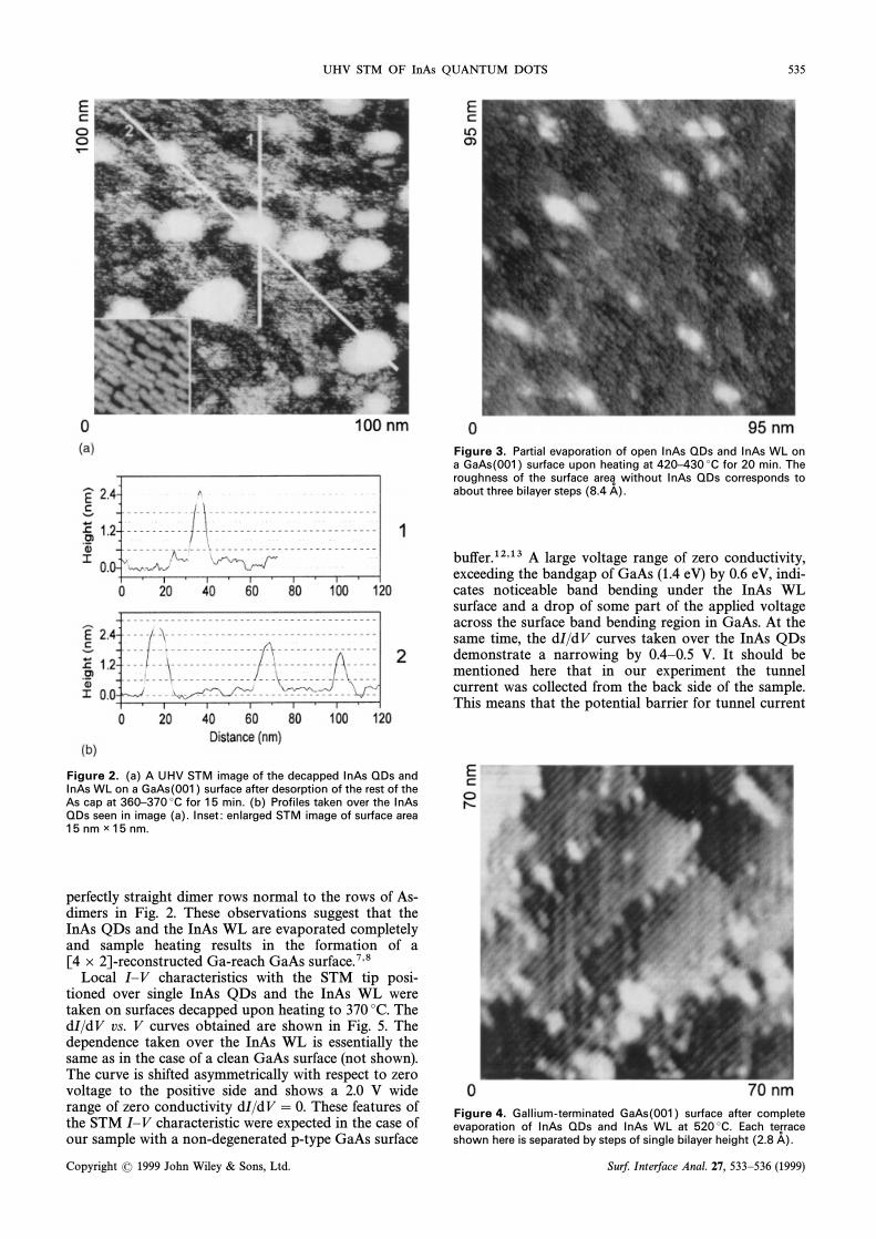
A strong indication that the open surface is indeedcovered with the InAs WL was obtained on furtherheating of the sample to higher temperatures. It can beseen in the STM image in Fig. 3 that on additionalheating of the sample at 420È430 ¡C for 20 min thesurface becomes rough and the As-dimer structure dis-appears. Moreover, the size and number of InAs QDson the surface su†er a dramatic reduction. This can beunderstood as being the result of evaporation of theInAs QDs and InAs WL in UHV on heating to tem-peratures higher than 400 ¡C. For comparison, note thatthe [2] 4] reconstruction of As-dimers in the case of aGaAs surface is stable even at 450 ¡C.6h8 The last STMimage in Fig. 4 was taken after an additional sampleheating to 520 ¡C for 15 min. This image again demon-strates a Ñat terrace arrangement of the surface, with
Surf. Interface Anal. 27, 533È536 (1999) Copyright ( 1999 John Wiley & Sons, Ltd.
UHV STM OF InAs QUANTUM DOTS 535
Figure 2. (a) A UHV STM image of the decapped InAs QDs andInAs WL on a GaAs(001) surface after desorption of the rest of theAs cap at 360–370 ¡C for 15 min. (b) Profiles taken over the InAsQDs seen in image (a). Inset : enlarged STM image of surface area15 nm Ã15 nm.
perfectly straight dimer rows normal to the rows of As-dimers in Fig. 2. These observations suggest that theInAs QDs and the InAs WL are evaporated completelyand sample heating results in the formation of a[4] 2]-reconstructed Ga-reach GaAs surface.7,8
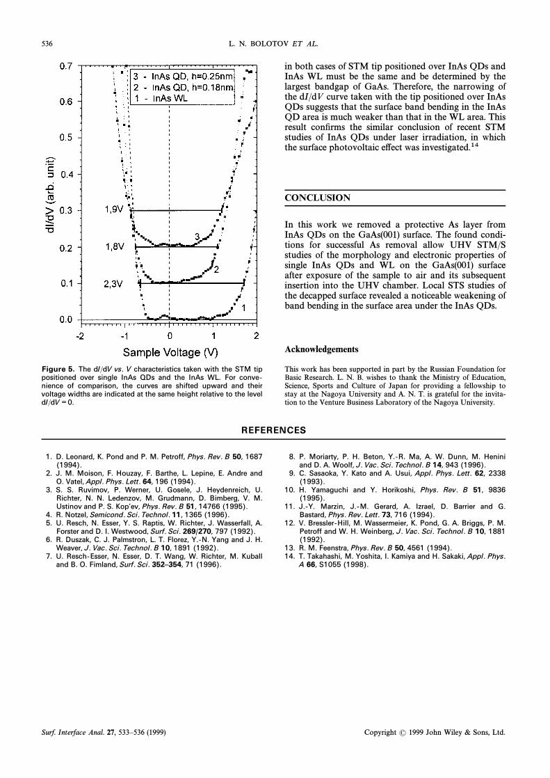
Local IÈV characteristics with the STM tip posi-tioned over single InAs QDs and the InAs WL weretaken on surfaces decapped upon heating to 370 ¡C. ThedI/dV vs. V curves obtained are shown in Fig. 5. Thedependence taken over the InAs WL is essentially thesame as in the case of a clean GaAs surface (not shown).The curve is shifted asymmetrically with respect to zerovoltage to the positive side and shows a 2.0 V widerange of zero conductivity dI/dV \ 0. These features ofthe STM IÈV characteristic were expected in the case ofour sample with a non-degenerated p-type GaAs surface
Figure 3. Partial evaporation of open InAs QDs and InAs WL ona GaAs(001) surface upon heating at 420–430 ¡C for 20 min. Theroughness of the surface area without InAs QDs corresponds toabout three bilayer steps (8.4 A� ).
bu†er.12,13 A large voltage range of zero conductivity,exceeding the bandgap of GaAs (1.4 eV) by 0.6 eV, indi-cates noticeable band bending under the InAs WLsurface and a drop of some part of the applied voltageacross the surface band bending region in GaAs. At thesame time, the dI/dV curves taken over the InAs QDsdemonstrate a narrowing by 0.4È0.5 V. It should bementioned here that in our experiment the tunnelcurrent was collected from the back side of the sample.This means that the potential barrier for tunnel current
Figure 4. Gallium-terminated GaAs(001) surface after completeevaporation of InAs QDs and InAs WL at 520 ¡C. Each terraceshown here is separated by steps of single bilayer height (2.8 A� ).
Copyright ( 1999 John Wiley & Sons, Ltd. Surf. Interface Anal. 27, 533È536 (1999)
536 L. N. BOLOTOV ET AL .
Figure 5. The dI /dV vs. V characteristics taken with the STM tippositioned over single InAs QDs and the InAs WL. For conve-nience of comparison, the curves are shifted upward and theirvoltage widths are indicated at the same height relative to the leveldI /dV ¼0.
in both cases of STM tip positioned over InAs QDs andInAs WL must be the same and be determined by thelargest bandgap of GaAs. Therefore, the narrowing ofthe dI/dV curve taken with the tip positioned over InAsQDs suggests that the surface band bending in the InAsQD area is much weaker than that in the WL area. Thisresult conÐrms the similar conclusion of recent STMstudies of InAs QDs under laser irradiation, in whichthe surface photovoltaic e†ect was investigated.14
CONCLUSION
In this work we removed a protective As layer fromInAs QDs on the GaAs(001) surface. The found condi-tions for successful As removal allow UHV STM/Sstudies of the morphology and electronic properties ofsingle InAs QDs and WL on the GaAs(001) surfaceafter exposure of the sample to air and its subsequentinsertion into the UHV chamber. Local STS studies ofthe decapped surface revealed a noticeable weakening ofband bending in the surface area under the InAs QDs.
Acknowledgements
This work has been supported in part by the Russian Foundation forBasic Research. L. N. B. wishes to thank the Ministry of Education,Science, Sports and Culture of Japan for providing a fellowship tostay at the Nagoya University and A. N. T. is grateful for the invita-tion to the Venture Business Laboratory of the Nagoya University.
REFERENCES
1. D. Leonard, K. Pond and P. M. Petroff, Phys. Rev. B 50, 1687(1994).
2. J. M. Moison, F. Houzay, F. Barthe, L. Lepine, E. Andre andO. Vatel, Appl . Phys. Lett . 64, 196 (1994).
3. S. S. Ruvimov, P. Werner, U. Gosele, J. Heydenreich, U.Richter, N. N. Ledenzov, M. Grudmann, D. Bimberg, V. M.Ustinov and P. S. Kop’ev, Phys.Rev.B 51, 14766 (1995).
4. R. Notzel, Semicond. Sci . Technol . 11, 1365 (1996).5. U. Resch, N. Esser, Y. S. Raptis, W. Richter, J. Wasserfall, A.
Forster and D. I. Westwood, Surf . Sci . 269/270, 797 (1992).6. R. Duszak, C. J. Palmstron, L. T. Florez, Y.-N. Yang and J. H.
Weaver, J . Vac. Sci . Technol . B 10, 1891 (1992).7. U. Resch-Esser, N. Esser, D. T. Wang, W. Richter, M. Kuball
and B. O. Fimland, Surf . Sci . 352–354, 71 (1996).
8. P. Moriarty, P. H. Beton, Y.-R. Ma, A. W. Dunn, M. Heniniand D. A. Woolf, J . Vac. Sci . Technol . B 14, 943 (1996).
9. C. Sasaoka, Y. Kato and A. Usui, Appl . Phys. Lett . 62, 2338(1993).
10. H. Yamaguchi and Y. Horikoshi, Phys. Rev. B 51, 9836(1995).
11. J.-Y. Marzin, J.-M. Gerard, A. Izrael, D. Barrier and G.Bastard, Phys.Rev. Lett . 73, 716 (1994).
12. V. Bressler-Hill, M. Wassermeier, K. Pond, G. A. Briggs, P. M.Petroff and W. H. Weinberg, J. Vac. Sci . Technol . B 10, 1881(1992).
13. R. M. Feenstra, Phys.Rev.B 50, 4561 (1994).14. T. Takahashi, M. Yoshita, I. Kamiya and H. Sakaki, Appl . Phys.
A 66, S1055 (1998).
Surf. Interface Anal. 27, 533È536 (1999) Copyright ( 1999 John Wiley & Sons, Ltd.