Embed Size (px)
Citation preview

2
Un-Cooled Microbolometers with Amorphous Germanium-Silicon
(a-GexSiy:H) Thermo-Sensing Films
Mario Moreno1, Alfonso Torres1, Roberto Ambrosio2 and Andrey Kosarev1 1National Institute of Astrophysics, Optics and Electronics, INAOE,
2Universidad Autonoma de Ciudad Juarez, UACJ, Mexico
1. Introduction
Silicon integrated circuits (IC) in conjunction with the micro-machining technology for thin films, have opened new ways for the development of low cost and reliable night vision systems based on thermal detectors. Among the thermal detectors used as pixels on IR focal plane arrays, the microbolometer appears as one of them. A microbolometer is a device in which the IR transduction is performed through a change in the resistivity of its thermo-sensing material, due to the heating effect caused by the absorbed radiation. Among the requirements for the materials used as thermo-sensing layer in microbolometers it can be mentioned a high activation energy (Ea), high temperature coefficient of resistance (TCR), low noise, and compatibility with standard CMOS fabrication processes. A variety of materials have been used as thermo-sensing elements in microbolometers, as vanadium oxide (VOx) (B. E. Cole, 1998, 2000), metals (A. Tanaka, 1996), polycrystalline (S. Sedky, 1998) and amorphous semiconductors (A. J. Syllaios, 2000).
Those materials have shown good characteristics but also some disadvantages. VOx has a moderated value of TCR (0.021 K-1) and low resistivty, however it is not a standard material in the IC technology. Metals as titanium are compatible with the standard IC technology, have low resistivity but also have very low TCR values. Polycrystalline semiconductors have high TCR values (0.05 K-1) and moderated resistivity, however they are deposited a relatively high temperatures (700 - 900 °C), which results in an incompatibility with a micro-bolometer fabrication post-process on a silicon wafer surface, containing an readout integrated circuit (ROIC).
Recently, it has been reported the study of W-doped VO2 (H. Takami, 2011) which has a TCR of above 0.1 k-1, and low resistivity values. However, this material is not standard on Si CMOS microelectronics facilities. GaAs/AlGaAs heterojunction bolometers (P.K.D.D.P. Pitigala, 2011) also have been reported, which have demonstrated TCR values of 0.04 K-1. However those structures are very complex, since they are fabricated with 30 periods of GaAs/Al0.57Ga0.43As junctions.
Hydrogenated amorphous silicon (a-Si:H) is a mature material on the microelectronics and photovoltaic industries. For un-cooled microbolometers a-Si:H is very attractive to be used
www.intechopen.com

Bolometers
24
as thermo-sensing material, since intrinsic a-Si:H has a very large activation energy (Ea) of above 1 eV, and therefore, provide a very large thermal coefficient of resistance (TCR) of 0.13 K-1. However intrinsic a-Si:H has a very low room temperature conductivity (┫RT ≤ 1x10⁻⁹ (Ωcm)-1), resulting in a very high pixel resistance when is used as thermo sensing material in microbolometers (Rpixel ≥ 109 Ω). Such high pixel resistance causes a mismatch with the input impedance of the CMOS ROIC. For commercial microbolometers, boron doping is commonly used in order to decrease the undesirable resistivity of intrinsic a-Si:H (A. J. Syllaios, 2000), to values of pixel resistance of around 30x106 Ω, however it also results on a reduction on the activation energy (Ea ≈ 0.22 eV) and on the TCR (-0.028 K-1), and therefore in a decrement on the pixel performance.
In our work we have studied the electrical and optical properties of amorphous germanium-silicon (a-GexSiy:H) and amorphous germanium-silicon-boron (a-GexSiyBz:H) thin films deposited by plasma (PECVD) (R. Ambrosio, 2004; A. Kosarev, 2006; A. Torres, 2008; M. Moreno, 2007, 2008, 2010). Intrinsic a-GexSiy:H has better performance characteristics than a-Si:H,B when is used as thermo-sensing element, since it has a high activation energy (Ea = 0.37 eV), a high TCR (┙ = -0.047 K-1), a moderated room temperature conductivity (┫RT ≈ 6x10⁻⁵ (Ωcm)-1), and therefore a moderated pixel resistance (Rpixel ≈ 30x107 Ω) (M. Moreno, 2007, 2008) when is used as thermo sensing element in microbolometers.
In the other hand a-GexSiyBz:H has an improved room temperature conductivity (┫RT ≈ 10-2-10-3 (Ωcm)-1), and therefore a moderated pixel resistance (Rpixel ≈ 1-5x10⁶ Ω) (M. Moreno, 2007, 2008), but also it has a low activation energy (Ea ≈ 0.18 - 0.22 eV) and low the TCR (-0.023 -0.028 K-1).
In this chapter we present a summary on the study of a-GexSiy:H and a-GexSiyBz:H thin films and their application as thermo-sensing element in microbolometers. We have fabricated, characterized and studied two devices configurations labeled as planar (the standard configuration used in commercial microbolometer arrays) and sandwich structures. The later shows several advantages when intrinsic materials are used as thermo-sensing element. Finally we studied the performance characteristics of the different device configurations and compared them with commercial devices and those reported on literature.
2. Principle of operation of un-cooled microbolometers
The operation of a microbolometer is based on the temperature rise of the thermo-sensing material by the absorption of the incident IR radiation. The change in temperature causes a change on its electrical resistance, which is measured by an external circuit. Microbolometers based on amorphous semiconductors have advantages over other types of thermal detectors, including microbolometers that use other kind of thermo-sensing materials. The advantages are mainly technological, since these microbolometers are fully compatible with silicon CMOS fabrication technology, there is no need of additional fabrication equipment in a IC production line. Are relatively of simple fabrication and can be processed at relatively low temperature by PECVD. The above make them ideal for a post-process fabrication over a CMOS read-out circuit.
Fig. 1 shows a scheme of one microbolometer (B. E. Cole, 1998); it is built on a membrane usually made of SiNx. Over the membrane is deposited the thermo-sensing material and the IR absorber material. The membrane provides thermal isolation to the thermo-sensing film.
www.intechopen.com

Un-Cooled Microbolometers with Amorphous Germanium-Silicon (a-GexSiy:H) Thermo-Sensing Films
25
Fig. 1. Microbolometer scheme.
2.1 Thermal insulation
There are three mechanism of heat transfer that occurs in a thermal detector, they are conduction, convection and radiation. Conduction mechanisms occur when the heat flows from the thermo-sensing area along the supporting legs to the substrate. Conduction is critical when the pixels are very close, since the heat can flow from one pixel to a neighbor pixel. Convection occurs when the heat flows in the presence of a surrounding atmosphere, this mechanism is not very important if the detector is encapsulated in a vacuum package. Radiation mechanism is presented by the fact that the detector radiates to its surroundings and the surroundings radiate to it.
When the microbolometers are encapsulated in an evacuated package, with an IR transmitting window, convection and radiation mechanism are minimized. Thus the main loss of heat mechanism is conduction from the thermo-sensing material to the substrate through the supporting structure.
The supporting structure is a very important part of thermal detectors, it provides three functions, mechanical support, electrical conducting path and thermal conducting path. In order to avoid heat losses in microbolometers, it is necessary to improve the thermal insulation. In microbolometers there are two main thermal insulation configurations: single-level and two-level configurations.
Single level configuration consist in deposit a membrane over the silicon (Si) substrate and after that, open a hole in the Si substrate, employing bulk micromachining techniques. Bulk micromachining consumes area, since the Si substrate is etched with a side wall angel of 54.9 degrees. The electronic circuit (which forms part of the read out circuit) is fabricated next to the pixel, consuming area also. That result in a 20% fill factor.
The two-level configuration allows the fabrication of the electronics circuit in the substrate and after that, the fabrication of the microbolometer in a low temperature post process over the electronics, by using surface micromachining techniques. With this configuration is saved substrate area, achieving a fill factor of above 70%.
In order to fabricate thermal sensors in a post process, over a wafer surface, containing an IC circuit; it is necessary to use low temperatures during the fabrication process. By employing
www.intechopen.com

Bolometers
26
Plasma Enhanced Chemical Vapor deposition (PECVD) it is possible to deposit thin films at relatively low temperatures (150 - 350 oC).
2.2 Infrared absorber films
An absorber element is a very important part in un-cooled IR microbolometers, its role is based in the absorption of IR radiation and the transfer of heat to the thermo-sensing material. The main requirements of absorbing materials for un-cooled microbolometers are: A high absorbance coefficient in the range ┣ = 8 – 12 ┤m, simple fabrication and compatibility with the silicon CMOS technology.
The IR absorption can be improved employing a resonant micro-cavity, where the thermo-sensing film is separated from the substrate by a gap equivalent to one quarter of the wavelength at which it will be operating. A mirror (Al or Ti) is deposited over the substrate surface, under the thermo-sensing material. In this configuration the radiation that was not absorbed by the thermo-sensing film will resound inside the cavity and will be re-absorbed by the thermo-sensing element.
Terrestrial objects have temperatures around of 300K, with IR emission centered in 10 ┤m. Thus un-cooled microbolometers employed for detection of objects at room temperature, should have a gap from the substrate of 2.5 ┤m, for the fabrication of the resonant micro-cavity.
Several materials have been employed as absorbing films in microbolometers, which are deposited over the thermo-sensing film. Among the most employed are some metals, as black gold film (M. Hirota, 1998), which has a very high absorption coefficient of IR radiation (more than 90 %), however it is not a standard material in CMOS technology. SiNx films are employed commonly as absorber films in microbolometers (A. Schaufelbühl, 2001, S. Sedky, 1998), since its absorption coefficient can be tuned by the deposition parameters and it is a standard material in CMOS technology.
2.3 Thermo-sensing films
The thermo-sensing material is perhaps the most important element in a microbolometer. The increment in temperature in the sensing material causes a change in some temperature-dependent parameter. In the case of a microbolometer that parameter is the resistance.
The thermo-sensing material should have a large temperature coefficient of resistance, TCR (┙(T)), which is defined by Eq. 1, where Ea is the activation energy, K is the Boltzman constant and T is temperature.
2aT 1 /R dR /dT E /KT (1)
A large TCR means that a small change in temperature in the sensing material will result in a large change in resistance. Eq. 1 shows that the TCR and Ea are directly related, thus a high Ea in the material is needed.
For un-cooled microbolometers vanadium oxide, VOx, was the first thermo-sensing element employed (B. E. Cole, 1998), since it has a moderated TCR, ┙(T) ≈ 0.021 K-1, however it is not a standard material in silicon CMOS technology. Some metals have been employed also,
www.intechopen.com
Un-Cooled Microbolometers with Amorphous Germanium-Silicon (a-GexSiy:H) Thermo-Sensing Films
27
which are compatible with Si-CMOS technology, however they have low values of TCR (Pt, ┙(T)≈0.0015 K-1).
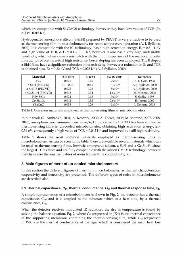
Hydrogenated amorphous silicon (a-Si:H) prepared by PECVD is very attractive to be used as thermo-sensing film in microbolometers, for room temperature operation (A. J. Syllaios, 2000). It is compatible with the IC technology, has a high activation energy, Ea ≈ 0.8 - 1 eV and high value of TCR, ┙(T) ≈ 0.1 – 0.13 K-1, however it also has a very high undesirable resistivity, which often cause a mismatch with the input impedance of the read-out circuits. In order to reduce the a-Si:H high resistance, boron doping has been employed. The B doped a-Si:H films have a significant reduction in its resistivity, however a reduction in Ea and TCR is obtained also, Ea ≈ 0.22 eV and TCR ≈ 0.028 K-1 (A. J. Syllaios, 2000).
Material TCR (K-1) Ea (eV) σRT (Ω cm)-1 Reference
VOx 0.021 0.16 2x10⁻¹ B. E. Cole, 1998
a-Si:H (PECVD) 0.1 - 0.13 0.8-1 ~ 1x10⁻⁹ A. J. Syllaios, 2000
a-Si:H,B (PECVD) 0.028 0.22 5x10⁻³ A. J. Syllaios, 2000
a-GexSiy:H (PECVD) 0.043 0.34 1.6x10⁻⁶ M. Moreno, 2008
Poly-SiGe 0.024 0.18 9x10⁻² S. Sedky, 1998
GexSi1-xOy 0.042 0.32 2.6x10⁻² E. Iborra, 2002
YBaCuO 0.033 0.26 1x10⁻³ J. Delerue, 2003
Table 1. Common materials employed as thermo-sensing films in microbolometers.
In our work (R. Ambrosio, 2004; A. Kosarev, 2006; A. Torres, 2008; M. Moreno, 2007, 2008, 2010), amorphous germanium-silicon, a-GexSiy:H, deposited by PECVD has been studied as thermo-sensing films in un-cooled microbolometer, obtaining high activation energy, Ea= 0.34 eV, consequently a high value of TCR = 0.043 K-1 and improved but still high resistivity.
Table 1 shows the most common materials employed as thermo-sensing films in microbolometers. As can be seen in the table, there are available several materials which can be used as thermo-sensing films. Intrinsic amorphous silicon, a-Si:H and a-GexSiy:H, show the largest TCR values and are fully compatible with the silicon CMOS technology, however they have also the smallest values of room temperature conductivity, ┫RT.
3. Main figures of merit of un-cooled microbolometers
In this section the different figures of merit of a microbolometer, as thermal characteristics, responsivity and detectivity are presented. The different types of noise in microbolometer are described also.
3.1 Thermal capacitance, Cth, thermal conductance, Gth and thermal response time, τth
A simple representation of a microbolometer is shown in Fig. 2, the detector has a thermal capacitance, Cth, and it is coupled to the substrate which is a heat sink, by a thermal conductance, Gth.
When the detector receives modulated IR radiation, the rise in temperature is found by solving the balance equation, Eq. 2; where Cth (expressed in JK-1) is the thermal capacitance of the supporting membrane containing the thermo sensing film, while Gth (expressed in WK-1) is the thermal conductance of the legs, which is considered the main heat loss
www.intechopen.com

Bolometers
28
Fig. 2. Microbolometer representation.
mechanism. ΔT is the temperature difference of the hot and reference junctions. Acell is the detector area, β is the fill factor, which is the radio of the thermo-sensing film area to the total cell area, η is the optical absorption coefficient, defined as the fraction of the radiant power falling on the thermo-sensing area, which is absorbed by that area. Po is the intensity of the IR modulated radiation, ω is the angular modulation frequency and t is time [2.6].
0th thC d T /dt G T expcellA P j t (2)
The solution of the balance equation is shown in Eq. 3:
02 2 1/2
th thT / G (1 )cellA P (3)
Where, ┬th (expressed in seconds) is the thermal response time of the microbolometer, it is defined by Eq. 4, which establishes a relation between ┬th, Cth and Gth. Typical values of thermal time constant are in the range of milliseconds, which are much longer than the typical time of photon detectors.
th th th C / G (4)
For unmodulated radiation Eq. 3 can be reduced to:
00 thT / GcellA P (5)
Eq. 5 shows that the increment of temperature, ΔT, in the detector is inversely proportional to the thermal conductance Gth of its legs. In order to achieve a high performance microbolometers ΔT should be as high as possible and therefore Gth as small as possible, which can be done by making very thin the detector legs.
3.2 Responsivity
Responsivity, R, is defined as the ratio of the pixel output signal to the incident radiant power (in Watts) falling on the pixel (P. W. Kruse, 2001). The output signal is an electrical signal that can be voltage or current, thus R can be expressed in Volts/Watts (voltage
www.intechopen.com
Un-Cooled Microbolometers with Amorphous Germanium-Silicon (a-GexSiy:H) Thermo-Sensing Films
29
responsivity, Ru) or Amps/Watts (current responsivity, RI). In order to obtain R, we can use the simplest model, where it is assumed that there is no heating due the electrical bias in the detector (Joulean heating), and also it is assumed a constant electrical bias to the detector.
When the microbolometer is current biased, the output signal is voltage, Vs, given by Eq. 6,
where Ib is the bias current, Rcell is the electrical resistance of the microbolometer, ┙ is the
TCR, described by Eq. 1 and ΔT is the increment of temperature in the detector, obtained in
Eq. 5.
Ts b cellV I R (6)
Voltage responsivity, Rv, is obtained by combining equations 3 and 6, and dividing by
PoAcell, which is the incident radiant power, the result is shown in Eq. 7.
1/22 2th th / G 1v b cellR I R (7)
th / Gv b cellR I R (8)
For unmodulated radiation, ω = 0, Eq. 7 is simplified in Eq. 8, which is the DC responsivity.
When the microbolometer is voltage biased equations 7 and 8 are transformed to Eq. 9 and
Eq. 10 respectively, where RI is current responsivity.
1/22 2th th / G 1I b cellR V R (9)
th / GI b cellR V R (10)
3.3 Noise in microbolometers
There are four main sources of noise in microbolometers (P. W. Kruse, 2001), which are
Johnson noise, 1/f noise, temperature fluctuation noise and background fluctuation noise,
these noise types are uncorrelated and are described in the following subsections.
3.3.1 Johnson noise
The Johnson noise component, Vj, is described by Eq. 11, where k is the Boltzmann constant,
Tcell is the bolometer temperature, Rcell is the bolometer resistance and Δf is the bandwidth of
the integration time.
1/2 4 fj cell cellV k T R (11)
3.3.2 1/f noise
The 1/f noise is characterized by a spectrum that depends inversely on frequency and is
described by Eq. 12, where V is the product of the bias current - Ib and the electrical
resistance of the microbolometer - Rcell, f is the frequency at which the noise is measured and
n is the 1/f noise parameter, which depend on the material detector.
www.intechopen.com
Bolometers
30
21
1/2
/ / fV V n f (12)
1/f noise is the dominant noise at low frequencies and falls below the Johnson noise at higher frequencies, the transition is commonly called the “knee”.
3.3.3 Temperature fluctuation noise
A thermal detector which is in contact with its environment (by conduction and radiation), exhibits random fluctuations in temperature, since the interchange of heat with its surrounding has a statistical nature; this is known as temperature fluctuation noise. The mean square temperature fluctuation noise voltage is given by Eq. 13 (P. W. Kruse, 2001).
1/22 2 2 2 2 2
TF cell thV 4kT f / G 1 V (13)
3.3.4 Background fluctuation noise
When the heat exchange by conduction between the detector and its surroundings is negligible, in comparison with the radiation exchange, the temperature fluctuation noise will be identified as background fluctuation noise.
The mean square background fluctuation noise is given by Eq. 14, where Tcell is the detector temperature and TB is the background temperature.
2 5 5 28 BF cell cell B cellV A k T T R (14)
The total noise voltage is obtained by adding the 4 noise contributions as is shown in Eq. 15.
2 2 2 2 21/ N f TF BFV Vj V V V (15)
3.4 Detectivity
Detectivity, D* (expressed in cmHz1/2Watt-1), is a figure of merit for all types of detectors, it
is defined as the pixel output signal to noise ratio per unit of incident radiant power falling
on the detector, measured in a 1 Hz bandwidth. In other words, D* is the normalized signal
to noise ratio in the detector and is shown in Eq. 16.
1 2/* / V cell f ND R A V (16)
In Eq. 16 Rv is the voltage responsivity, Acell is the detector area, Δf is the frequency bandwidth and VN is the contribution of the four noises. It is clear that in order to achieve a high D* the responsivity should be as high as possible and the noise as small as possible.
The fundamental limit to sensitivity of any thermal detector is set by random fluctuations in the temperature of the detector due to fluctuations in the radiant power exchange between the detector and its surroundings. The highest possible value of D* of a thermal detector operated at room temperature is D* = 1.98 x10¹⁰ cmHz1/2W-1(A. Rogalski, 2003).
www.intechopen.com

Un-Cooled Microbolometers with Amorphous Germanium-Silicon (a-GexSiy:H) Thermo-Sensing Films
31
4. Amorphous germanium-silicon (a-GexSiy:H) and germanium-silicon-boron alloys (a-GexSiyBz:H)
Intrinsic amorphous silicon (a-Si:H) prepared by PECVD is a very attractive material to be used in microbolometers as thermo-sensing film. It has a high activation energy, Ea ≈ 0.8 - 1 eV and high value of temperature coefficient of resistance, TCR, ┙(T) ≈0.1 - 0.13 K-1, however it also has a high undesirable resistivity.
Amorphous germanium-silicon (a-GexSiy:H) films deposited by PECVD have been studied as thermo-sensing film in microbolometers (R. Ambrosio, 2004; A. Kosarev, 2006; A. Torres, 2008; M. Moreno, 2007, 2008, 2010), due its high activation energy and consequently high TCR, and its relatively high room temperature conductivity, ┫RT, in comparison with a-Si:H films. In this section is presented a description of the deposition by PECVD of intrinsic amorphous germanium-silicon (a-GexSiy:H) and amorphous germanium-silicon-boron (a-GexSiyBz:H) thin films, and its electrical and compositional characterization.
4.1 Films preparation for characterization
An intrinsic film (a-GexSiy:H) was deposited in a capacitive discharge low frequency (LF) PECVD reactor at frequency f = 110 KHz, substrate temperature Ts = 300 oC, pressure P = 0.6 Torr and RF power W = 350 W, with a gas mixture of SiH4, GeH4 and H2 and gas flow rates of QSiH4=25 sccm, QGeH4 =25 sccm and QH2=1000 sccm respectively. This result in a Ge gas content Xg = 0.5. The film was labeled as process A.
The a-GexSiyBz:H films were also deposited in a capacitive discharge low frequency (LF) PECVD reactor at frequency f = 110 KHz, substrate temperature Ts = 300 oC, pressure P = 0.6 Torr and RF power W = 350 W. Three sets of films were deposited from SiH4 (100%), GeH4 (100%) and B2H6 (1% on H2) gas mixture, with a fixed SiH4 and B2H6 gas flow rates: QSiH4=50sccm and QB2H6=500 sccm, respectively, while the GeH4 gas flow was set at the following values: QGeH4 =25, 50 and 75 sccm.
The late resulted in a Ge gas content Xg= 0.3, 0.45, 0.55 and a B gas content Zg= 0.11, 0.09, 0.07 in the samples labeled as process number B, C and D, respectively. Table 2 shows the deposition parameters for the 4 thermo-sensing films.
Process A (intrinsic)
Process B Process C Process D
Gases flow rates (sccm) SiH4(100%): 25 GeH4(100%):25
H2: 1000
SiH4 (100%): 50 GeH4(100%):
25 B2H6 (1%): 500
SiH4 (100%): 50 GeH4(100%):
50 B2H6 (1%): 500
SiH4 (100%): 50 GeH4(100%):
75 B2H6 (1%): 500
Dilution ratio (%): _______H2_____
GeH4+SiH4+B2H6 20 6.2 4.7 3.8
Ge contentin gas mixture (%) 50 30 45 55 B contentin gas mixture (%) ---- 11 9 7
Temperature (°C) 300°C 300°C 300°C 300°C Pressure (Torr.) 0.6 0.6 0.6 0.6
Frequency (Khz.) 110 110 110 110 Power (W) 300 300 300 300
Table 2. Deposition parameters of a-GexSiy:H and a-GexSiyBz:H films.
www.intechopen.com

Bolometers
32
Since those films are studied for applications as thermo-sensing films for microbolometers, we measured the film electrical properties after patterning them with photolithography in one cell of dimensions 70 x 66 ┤m2.
Assuming that stress arisen in the film deposited over a SiNx micro-bridge could have an effect on the film conductivity, we also studied the films deposited on a micro-bridge. For that purpose, we prepared three different kinds of samples for each type of the four thermo-sensing films (three boron alloys with different Ge content and the intrinsic film). The films were prepared as is shown in Fig. 3.
A) Stripes sample B) Patterned sample C) Micro-bridge sample
Fig. 3. Different thermo-sensing films samples. A) Stripes, B) pattern and C) Micro-bridge.
4.2 Temperature dependence of conductivity and TCR in a-GexSiy:H and a-GexSiyBz:H films
We performed measurements of temperature dependence of conductivity ┫(T) in the a-GexSiy:H and a-GexSiyBz:H thermo-sensing films in the range of T= 300–400 K. The measurements were performed in a vacuum chamber at a pressure P≈20 mTorrs. A temperature controller (model K-20, MMR Inst.) for the temperature measurement control and an electrometer (model 6517-A, Keithley Inst.) for the current measurements were employed. These measurements allowed us to obtain the ┫(T) temperature dependence and then to determine the Ea, the TCR and the room temperature conductivity, ┫RT.
The conductivity temperature dependence can be well described by ┫(T)=┫0 exp(-Ea/kT),
where ┫0 is the prefactor, Ea is the activation energy, k is the Boltzmann constant and T is the
temperature. Fig. 4 shows ┫(T) curves for four different thermo-sensing films (three boron
alloys with different Ge gas content, Gex = 0.3, 0.45, 0.55 and the intrinsic film with Gex = 0.5),
fabricated in three different sample configurations (stripes, patterns and micro-bridges).
From ┫(T) measurements with temperature in the thermo-sensing films, we found that the boron alloys (a-GexSiyBz:H) have a significantly larger conductivity (by about 2-3 orders of magnitude) in comparison with that of the intrinsic film (a-GexSiy:H). We observed that an increment in the Ge content in gas phase in the boron alloys results in an increase of the room temperature conductivity, from ┫RT = 2.8 x10⁻³ (Ωcm)-1 (for Gex = 0.3) to ┫RT = 1 x10⁻²
(Ωcm)-1 (for Gex = 0.45) and ┫RT = 2.5 x10⁻² (Ωcm)-1 (for Gex = 0.55), while for the intrinsic film the room temperature conductivity is ┫RT = 6 x10⁻⁵ (Ωcm)-1 (for Gex = 0.5).
www.intechopen.com

Un-Cooled Microbolometers with Amorphous Germanium-Silicon (a-GexSiy:H) Thermo-Sensing Films
33
Fig. 4. Conductivity dependence with temperature for the different thermo-sensing films (process: A, B, C and D).
The increment in the ┫ is accompanied with a reduction in the Ea. We obtained an Ea= 0.22 eV (for Gex = 0.3), Ea= 0.21 eV (for Gex = 0.45) and Ea= 0.18 eV (for Gex = 0.55), while in the intrinsic film is Ea= 0.345 eV (for Gex = 0.5). Ea as a function of Gex is shown in Fig. 5 A).
The reduction in the thermo-sensing films dimensions, from the stripes samples (10x1.5 mm2) to the patterned samples (70 x 66 ┤m2), has no significant effect on Ea, however it has on the ┫RT. We observed a reduction of above 50-80 % of the ┫RT value in the patterned samples in comparison with that of the stripes samples.
Practically no change in Ea of the thermo-sensing films deposited over a SiNx micro-bridge was observed, in comparison with that of the stripes and patterned samples; however the micro-bridge samples showed a larger reduction in the ┫RT values, of 60-90 %. The dependence of ┫RT with the Gex content and the sample structure are shown in Fig. 5 B), while the deposition rate dependence of Gex content in the thermo-sensing films is shown in Fig. 5 C). Table 3 show a comparison of Ea, TCR, ┫RT and ┫0 in stripes, patterned and micro-bridges samples for the different thermo-sensing films.
The micro-bridges samples have the largest reduction of conductivity, and it could be explained by the stress arisen in the SiNx micro-bridge, affecting the thermo-sensing film electrical conductivity. The deposition rate in the boron alloys is around 2 -3 times larger than that of the intrinsic film. Boron incorporation during the thermo-sensing deposition, enhance the deposition rate as is shown in Fig. 5 C).
www.intechopen.com

Bolometers
34
Fig. 5. Characterization of a-GexSiy:H and a-GexSiyBz:H films. A) Ea as function of Ge gas content (Gex). B) Conductivity as a function of Ge gas content. C) Deposition rate as a function of Ge gas content.
It is important to point out that, doping on amorphous semiconductors reduce Ea and
increases the films conductivity (┫RT). In Fig 5A) for reference, is shown an intrinsic a-
GexSiy:H film produced with a gas content of Gex=50% and Siy=50%, which has a Ea of 0.34
eV. This is the largest value for a-GexSiy:H films (doped or un-doped, using a gas content of
Gex=50% and Siy=50%).
When boron is introduced in the film deposition, Ea is reduced and the conductivity is increased in the films. In fig. 5 A) is shown that Ea is reduced to values in the range of 0.18 - 0.22 eV, while the conductivity is increased in more than one order of magnitude. Also it is important to notice that a-GexSiy:H films have an intermediate Ea value, between a-Si:H and a-Ge:H. Intrinsic a-Si:H has Ea values close to 1 eV, while a-Ge:H have Ea values of above 0.3 eV. Thus, varying the Ge (and Si) gas contents in the a-GexSiy:H films, it is possible to modify Ea (an also the conductivity) on intrinsic films.
Larger Gex content in the films will reduce the value of Ea. In fig 5 A), we observe a decrement on Ea of the a-GexSiyBz:H films, not just because the Bz gas content (which in fact decreases), but because the Ge content (which increases). In fig 5 A) is shown that for a-GexSiyBz:H films, the Gex gas content vary between 0.3 and 0.55, while the Bz gas content
www.intechopen.com

Un-Cooled Microbolometers with Amorphous Germanium-Silicon (a-GexSiy:H) Thermo-Sensing Films
35
vary just between 0.07 and 0.11. Thus the effect of the variation of the Ge gas content on Ea is dominant in the a-GexSiyBz:H films .
4.3 Composition of the a-GexSiy:H and a-GexSiyBz:H films
In Figure 5 the showed results are related to the Gex, Siy, and Bz gas contents, not to solid contents. There exists a significant difference between the gas content used for the films deposition, and the solid content in the films produced. The composition in solid phase of the different films (three boron alloys with different Ge gas content and the intrinsic film) was characterized by secondary ion mass spectroscopy (SIMS). The samples used for SIMS characterization were the stripes samples described in section 4.1. Fig. 6 shows the SIMS profiles obtained.
From SIMS profiles we calculated the solid composition in the thermo-sensing films. For the film with gas content: Gex=0.3 and Bz=0.11 (process B), we observed an increase in the solid content: Gex=0.59 and Bz=0.32 respectively. For the film with Gex=0.45 and Bz=0.09 (process C), we observed Gex=0.67 and Bz=0.26, respectively. For the film with Gex=0.55 and Bz=0.07 (process D), we observed Gex=0.71 and Bz=0.23, respectively. These results suggested a strong preferential B and Ge incorporation from gas phase during the film deposition process. The Bz solid content demonstrated values about 3 times larger than the content in gas phase Bz, while the Gex solid content increased by a factor of 1.3-2 from the Gex gas content. Those results are shown in Table 4.
Thermo-sensing films
Process A Process B Process C Process D
Film Thickness (μm) 0.5 0.36 0.42 0.51
Deposition rate (A/s) 2.8 6 7 9.5
Stripes samples
Ea (eV) 0.345 0.22 0.21 0.18
TCR (K-1) -0.044 -0.028 -0.027 -0.023
σRT (Ωcm)-1 6x10⁻⁵ 2.8x10⁻³ 1x10⁻² 2.5x10⁻²
σ0 (Ωcm)-1 34.85 12.02 36.46 24.55
Patterned samples
Ea (eV) 0.36 0.225 0.20 0.20
TCR (K-1) -0.046 -0.029 -0.025 -0.025
σRT (Ωcm)-1 1.08x10⁻⁵ 1.4x10⁻³ 4x10⁻³ 1.2x10⁻²
σ0 (Ωcm)-1 11.13 7.27 8.23 28.26
Micro-bridge samples
Ea (eV) 0.37
Not available
0.22 0.20
TCR (K-1) -0.047 -0.028 -0.025
σRT (Ωcm)-1 2.2x10⁻⁵ 1.2x10⁻³ 7x10⁻³
σ0 (Ωcm)-1 32.8 5.94 15.58
Table 3. Comparison of Ea, TCR, ┫RT and ┫0 in stripes, patterned and micro-bridges samples for the different thermo-sensing films.
In Fig. 6 the intrinsic film has a Boron content of 1018 cm-3 (which represents a B solid content of 2x10⁻³ %) as is shown in table 4. The reason of the above is the fact that all the films were deposited on the same chamber. Even though, the chamber was extensively cleaned and coated with a SiNx film before the intrinsic film deposition, Boron impurities remained in the chamber walls, which were re-deposited in the intrinsic films.
www.intechopen.com

Bolometers
36
Fig. 6. SIMS profiles of a-GexSiy:H and a-GexSiyBz:H thermo-sensing films.
Thermo-sensing films
Process A Process B Process C Process D
Gas content
Gex (%) 0.5 0.3 0.45 0.55
Siy (%) 0.5 0.59 0.46 0.38
Bz (%) 0 0.11 0.09 0.07
Solid content obtained from SIMS
Gex (%) 0.888 0.59 0.67 0.71
Siy (%) 0.110 0.078 0.05 0.04
Bz (%) 2.0x10⁻³ 0.32 0.26 0.23
Table 4. Gas content and solid content obtained by SIMS for the thermo-sensing films.
5. Microbolometer configurations and fabrication process flow
In this section we show a comparative study of the performance characteristics of three configurations of un-cooled microbolometers based on amorphous germanium thin films: a) Planar structure with intrinsic amorphous germanium-silicon a-GexSiy:H thermo-sensing film. In this configuration the metal electrodes are placed under the thermo-sensing film (Fig. 7 A); b) Planar structure with amorphous germanium-boron-silicon alloy a-GexBySiz:H thermo-sensing film (Fig. 7 B) and c) Sandwich structure with intrinsic a-GexSiy:H thermo-sensing film, this configuration consists of metal electrodes which sandwich the thermo-sensing film (Fig. 7 C). Fig. 7 D) shows a picture of one device fabricated.
www.intechopen.com

Un-Cooled Microbolometers with Amorphous Germanium-Silicon (a-GexSiy:H) Thermo-Sensing Films
37
The fabrication process of the planar structure microbolometer with the a-GexSiy:H thermo-sensing film is as follows. A 0.2 ┤m-thick SiO2 layer is deposited by CVD on a c-Si wafer and a 2.5 m-thick sacrificial aluminum layer is deposited by e-beam evaporation and patterned. A 0.8 m-thick SiNx film is then deposited at low temperature (350 oC) by low frequency PECVD over the aluminum sacrificial film. The SiNx film is patterned by reactive ion etching (RIE) in order to form a SiNx bridge. A 0.2 ┤m-thick titanium contacts are deposited by e-beam evaporation over the SiNx bridge and a 0.5 m-thick thermo-sensing a-GexSiy:H film is deposited over the Ti contacts by low frequency LF PECVD technique at a rf frequency f=110 kHz, temperature T=300 oC, power W=350 W and pressure P=0.6 Torr. The a-GexSiy:H film is deposited from a SiH4 + GeH4 + H2 mixture with gas flows: QSiH4=25sccm, QGeH4 =25 sccm, QH2=1000 sccm. This results in a Ge content in solid phase Y=0.88 and a Si content in solid phase Y=0.11. The thermo-sensing film is covered with a 0.2 m-thick absorbing SiNx film deposited by PECVD and finally the aluminum sacrificial layer is removed with wet etching.
The planar structure microbolometer with the boron alloy (a-GexBySiy:H) thermo-sensing film is fabricated as the previous one, with difference in the thermo-sensing film deposition parameters. The boron alloy film is deposited from a SiH4 + GeH4 + B2H6 + H2 mixture with the following gas flows: QSiH4=50sccm, QGeH4 =50 sccm, QB2H6=5 sccm and QH2=500 sccm. This results in a Ge content in solid phase Gex=0.67 and B content in solid phase By=0.26. Those values were obtained by SIMS measurements.
Fig. 7. Microbolometers: A) Planar wit intrinsic film a-GexSiy:H, B) Planar with boron doped film a-GexBySiz:H, C) Sandwich with intrinsic film a-GexSiy:H, D) A device fabricated.
The sandwich structure microbolometer with the a-GexSiy:H film is fabricated in the same way as the planar microbolometer with some differences, due to the placing of metals as
www.intechopen.com

Bolometers
38
bottom and top electrodes. In this structure the electrodes sandwich the thermo-sensing film. The bottom Ti electrode is 0.2 ┤m-thick and is deposited before the thermo-sensing film. Then the a-GexSiy:H film is deposited and it is covered with a top thin electrode (10 nm) forming a sandwich structure. The active area of the thermo-sensing layer in the three
configurations studied is Ab=70x66m2. Fig. 8 shows the fabrication process of the microbolometer structures.
Fig. 8. Planar and sandwich microbolometers fabrication process flow.
www.intechopen.com
Un-Cooled Microbolometers with Amorphous Germanium-Silicon (a-GexSiy:H) Thermo-Sensing Films
39
6. Microbolometers electrical characterization
A microbolometer is a resistor sensitive to temperature change, its operation is based on the temperature increase of the thermo-sensing film by the absorption of the incident IR radiation. The change in temperature causes a change on its electrical resistance, which is measured by an external circuit.
In this section we present a comparative study of 3 configurations of un-cooled microbolometers based on amorphous silicon-germanium thin films deposited by plasma.
6.1 I(U) measurements in dark and under Infrared Radiation (IR)
In this section is described the procedure performed in order to obtain the current voltage I(U) characteristics of the microbolometers, from this measurement it is possible to determine the microbolometer electrical resistance and responsivity.
The current-voltage characteristics I(U) and current noise spectral density (NSD) have been measured in the devices in order to compare the performance characteristics, such as responsivity and detectivity in the 3 configurations of microbolometers:
a. Planar structure with an intrinsic germanium-silicon (a-GexSiy:H, Gex=0.5) thermo-sensing film (process A of section 4).
b. Planar structure with a germanium-silicon-boron alloy (a-GexSiyBz:H, Gex=0.45, Bz=0.09) thermo-sensing film (process C of section 4).
c. Sandwich structure with an intrinsic (a-GexSiy:H, Gex=0.5) thermo-sensing film (process A of section 4).
The samples were placed in a vacuum chamber at pressure P20 mTorr, at room temperature and illuminated through a zinc selenide window (ZnSe). The window has a 70% transmission in the range of ┣=0.6 – 20 µm. The source of IR light is a SiC globar source, which provides intensity I0=5.3x10⁻² W/cm2 in the range of ┣=1 – 20 µm. The current was measured with an electrometer (“Keithley”- 6517-A) controlled by a PC in dark and under IR illumination.
Fig. 9 A) shows the current-voltage I(U) characteristics in dark and under IR illumination for the planar configuration with a-GexSiy:H thermo-sensing film (process A, section 4); Fig. 9 B) shows these characteristics for the planar configuration with a-GexSiyBz:H thermo-sensing film (process C, section 4); and Fig. 9 C) shows the same characteristics for the sandwich configuration with a-GexSiy:H thermo-sensing film (process A, section 4).
In those figures we can see the increment in current due to IR illumination, ∆I=IIR–IDark, where IIR is the current under IR radiation and IDark is the current in dark. The planar configuration with the a-GexSiy:H (Gex=0.5) film has a ∆I = 5.4 nA (at bias voltage U=7 V); the planar configuration with the a-GexSiyBz:H (Gex=0.45, Bz=0.09) film has a ∆I = 65 nA (at bias voltage U=7 V); and the sandwich configuration with the a-GexSiy:H (Gex=0.5) film has a ∆I = 35 ┤A (at bias voltage U=4 V). The inset in those figures show the Log I(Log U) characteristics, where we can see their linear behavior. The gamma (┛) constant indicates the slope of the curves.
6.2 Current and voltage responsivity
The current responsivity, RI, is described by Eq. 17, where ∆I is the increment in current (∆I=IIR–IDark) and Pincident is the IR incident power in the device surface. Pincident is described by Eq. 18 and is the product of the cell area, Acell and the IR source intensity, I0.
www.intechopen.com

Bolometers
40
I incidentR I / P (17)
0incident cellP A I (18)
The intensity of the IR source is I0 = 0.053 Wcm-2, while the cell area is Acell = (70x10-4)(66x10-
4) cm2 = 4.6x10⁻⁵ cm2. Therefore the IR incident power in the device surface is Pincident = 2.475x10⁻⁶ W. The planar microbolometer with a-GexSiy:H (Gex=0.5) film has a RI=2x10⁻³ A/W (at U=7 V); the planar microbolometer with a-GexSiyBz:H (Gex=0.45, Bz=0.09) film has a RI= 3x10⁻² A/W (at U=7 V); and the sandwich microbolometer with a-GexSiy:H (Gex=0.5) film has a RI= 14 A/W (at U=4 V).
Table 5 shows the ∆I and RI values obtained in the configurations. Fig. 10 A) shows the voltage dependence of RI for the planar microbolometer with a-GexSiy:H (Gex=0.5) film; Fig. 10 B) shows the voltage dependence of RI for the planar microbolometer with a-GexSiyBZ:H (Gex=0.45, Bz=0.09) film; and Fig. 10 C) shows the voltage dependence of RI for the sandwich microbolometer with a-GexSiy:H (Gex=0.5) film. The insert in those figures show a relative current responsivity. Relative current responsivity is the ratio between the increment of current from dark to IR condition, ΔRI, and the microbolometer resistance Rcell.
Fig. 9. I(U) characteristics of 3 microbolometers: A) planar with a-GexSiy:H (Gex=0.5). B) planar with a-GexSiyBZ:H (Gex=0.45, Bz=0.09). C) sandwich with a-GexSiy:H (Gex=0.5). The inset in those figures show the Log I(Log U) characteristics, where we can see their linear behavior. The gamma (┛) constant indicates the slope of the curves.
www.intechopen.com

Un-Cooled Microbolometers with Amorphous Germanium-Silicon (a-GexSiy:H) Thermo-Sensing Films
41
The planar and sandwich structures with the intrinsic film show larger values of relative
current responsivity. The voltage responsivity, RU, was calculated from the experimental
I(U) points, the increment in voltage from dark condition to IR condition was obtained from
a fixed current. Fig. 11 A) shows a ∆U= 1.8 V extracted from a fixed current I = 1.5x10⁻⁸ A, in
the planar structure microbolometer with the a-GexSiy:H (Gex=0.5) film. Fig. 11 B) shows a
∆U= 0.3 V extracted from a fixed current I = 1.35x10⁻⁶ A, in the planar structure
microbolometer with the a-GexSiyBZ:H (Gex=0.45, Bz=0.09) film. Fig. 11 C) shows a ∆U= 0.54
V extracted from a fixed current I = 1.16x10⁻⁴ A, in the sandwich structure microbolometer
with the a-GexSiy:H (Gex=0.5) film.
Planar
structureWith a-GexSiy:H
Planar structureWith a-GexSiyBz:H
Sandwich structureWith
a-GexSiy:H
Film process A C A
∆I= IIR – Idark (A) 5.4 x10⁻⁹ (at U=7 V) 65x10-9 (at U=7 V) 35x10-6 (at U=4 V)
Current responsivity (AW-1) 2x10⁻³ 3x10⁻² 14
∆U= UIR – Udark (V) 1.8 (at I=1.5x10⁻⁸) 0.3 (at I=1.35x10⁻⁶) 0.54 (at I=1.16x10⁻⁴)
Voltage Responsivity (VW-1) 7.2x10⁵ 1.2x10⁵ 2.2x10⁵
Table 5. Current and voltage responsivity values for 3 microbolometer configurations.
Fig. 10. Voltage dependence of RI of 3 microbolometers: A) planar with a-GexSiy:H (Gex=0.5). B) planar with a-GexSiyBZ:H (Gex=0.45, Bz=0.09). C) sandwich with a-GexSiy:H (Gex=0.5).
www.intechopen.com

Bolometers
42
The planar microbolometer with a-GexSiy:H (Gex=0.5) film has a RU=7.2x10⁵ V/W (at
I=1.5x10⁻⁸ A); the planar microbolometer with a-GexSiyBz:H (Gex=0.45, Bz=0.09) film has a
RU= 1.2x10⁵ V/W (at I=1.4x10⁻⁶ A); and the sandwich microbolometer with a-GexSiy:H
(Gex=0.5) film has a RU= 2.2x10⁵ V/W (at I=1.16x10⁻⁴ A). Table 5 shows the ∆U and RU values
obtained from the different microbolometers configurations.
Fig. 11. Extraction of ∆U from I(U) characteristics: A) planar with a-GexSiy:H (Gex=0.5). B)
planar with a-GexSiyBZ:H (Gex=0.45, Bz=0.09). C) sandwich with a-GexSiy:H (Gex=0.5).
6.3 Noise spectral density measurements and detectivity calculations
Noise measurements in the microbolometers were performed with a lock-in amplifier
(“Stanford Research Systems” - SR530). The noise of the system and the total noise (system +
cell noise) were measured separately, and a subtraction of the system noise allowed us to
obtain the noise of the device. The detectivity was calculated from the responsivity values
and noise measurements. The current noise spectral density (NSD), Icell noise (f), of the
fabricated devices with the different thermo-sensing films are shown in Fig. 12.
The NSD in the cell is obtained as (Icell noise(f))2 = (Isystem + cell noise(f))2 – (Isystem noise(f))2, where
Icell + system noise(f) is the NSD measured at the microbolometer with the measuring system and
the Isystem noise(f) is the NSD measured in the system without the microbolometer. In noise
www.intechopen.com

Un-Cooled Microbolometers with Amorphous Germanium-Silicon (a-GexSiy:H) Thermo-Sensing Films
43
curves we observed different slopes at different frequencies and different cone frequencies.
That data are shown in Table 6, where fc1 is the cone frequency 1, fc2 is the cone frequency
2, ┚ is the slope of the curve in region 1 and ┛ is the slope of the curve in region 2.
The planar structure with a-GexSiy:H (Gex=0.5) film shows Icell noise (f) ≈ 10-16 AHz-1/2; the
planar structure with a-GexSiyBz:H (Gex=0.45, Bz=0.09) film shows Icell noise (f) ≈ 10-14 AHz-1/2;
and the sandwich structure with a-GexSiy:H (Gex=0.5) has Icell noise (f) ≈ 10-11 AHz-1/2.
The procedure for the detectivity calculation is shown in Eq. 19, where RI is the current
responsivity, Acell is the detector area, Inoise is the cell NSD and ∆f = 1 is the bandwidth of the
measurement system.
1 2 1 2/ ) /* / /(I cell noiseD R A I f (19)
Fig. 12. Spectral density of current noise (NSD) of 3 microbolometers: A) planar with a-GexSiy:H (Gex=0.5). B) planar with a-GexSiyBZ:H (Gex=0.45, Bz=0.09). C) sandwich with a-GexSiy:H (Gex=0.5).
We calculated the detectivity values D* in the 3 structures. For the planar structure with the
a-GexSiy:H (Gex=0.5) film we obtained D*= 7x10⁹ cmHz1/2W-1; for the planar structure with
the a-GexSiyBz:H (Gex=0.45, Bz=0.09) film it is D*= 5.9x10⁹ cmHz1/2W-1; and for the sandwich
structure microbolometer with the a-GexSiy:H (Gex=0.5) film it is D*= 4x10⁹ cmHz1/2W-1.
www.intechopen.com

Bolometers
44
Samples
Frequency Regions
Region no. 1 Region no. 2 Region no. 3
┚ fc1 (Hz.) ┛ fc2 (Hz.) Noise level (AHz-1/2)
Planar structure a-GexSiy:H (Gex=0.5)
0.47 23 1.34 350
10-16
Planar structure a-GexSiyBz:H (Gex=0.45, Bz=0.09)
0.9 2 1.04 100 10-14
Sandwich structure a-GexSiy:H (Gex=0.5)
0.15 5 0.98 30 10-11
Table 6. NSD at different frequency regions in the different microbolometers structures.
7. Microbolometers thermal characterization and calibration curve
In order to estimate the temperature dependence of the thermal resistance of the microbolometers, I(U) measurements were performed in the range from 260 K to 360 K, as is shown in Fig. 13 A), where the bias is plotted as a function of current.
Fig. 13. A) U(I) curves of a planar structure microbolometer with a-GexSiy:H (Gex=0.5). B) Calibration curve of a planar structure microbolometer with a-GexSiy:H (Gex=0.5).
The slope of the linear part of each curve showed in Fig. 13 A) corresponds to the electrical
resistance of the microbolometer for each temperature value (in the range of 260 K - 360 K).
Once that is obtained the value of the electrical resistance for each value of temperature, it is
possible to graph the electrical resistance of the microbolometer as a function of the
temperature, also called the calibration curve, as is shown in Fig. 13 B).
The calibration curve is very important because from this curve is possible to calculate an
increment in temperature in the microbolometer by measuring a change in its resistance.
The voltage-current curves in Fig. 13 A) have different resistance values as the current
increases. The value of the resistance is affected by the temperature. Thus the resistance is
calculated for each point of the Voltage-Current curves (obtained at different temperatures,
260, 270, etc.). If the resistance values obtained are compared with the calibration curve, it is
possible to extract the increment of temperature (ΔT) for each point.
www.intechopen.com

Un-Cooled Microbolometers with Amorphous Germanium-Silicon (a-GexSiy:H) Thermo-Sensing Films
45
Fig. 14 A) shows the increment of temperature (ΔT) as a function of the power (P=U*I) applied to the microbolometer, for each temperature.
Fig. 14. A) ΔT vs Power curve of a microbolometer. B) Thermal resistance of a planar structure microbolometer with a-GexSiy:H (Gex=0.5).
Fig. 15. Microbolometer with a-GexSiyBz:H (Gex=0.45, Bz=0.09). A) Calibration curve. B) Thermal resistance.
The thermal resistance of the microbolometer, Rth, is then obtained as the slope of the increment of temperature in the microbolometer (ΔT) as a function of the power applied to it, for each temperature value. Fig. 14 B) shows the temperature dependence of the thermal
resistance (Rth). Fig. 15 A) shows the calibration curve and Fig. 15 B) shows the temperature dependence of the thermal resistance (Rth) of the planar structure microbolometer with a-GexSiyBz:H (Gex=0.45, Bz=0.09).
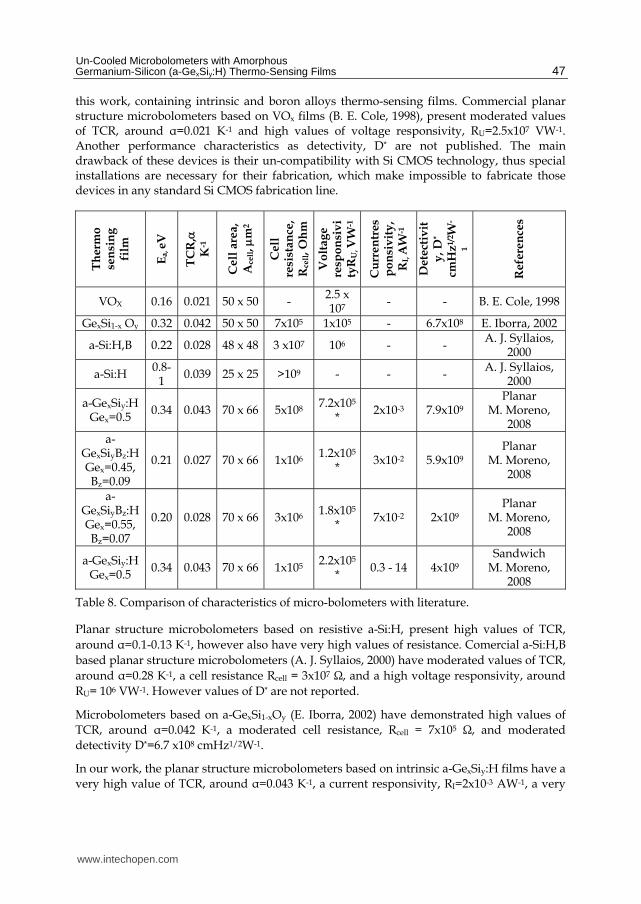
8. a-GexSiy:H and a-GexSiyBz:H microbolometers compared with literature
The results obtained from the study of fabrication and characterization of different microbolometer structures, containing intrinsic a-GexSiy:H films and boron alloys a-GexSiyBz:H, are discussed in the present section and compared with data reported in literature.
www.intechopen.com

Bolometers
46
8.1 Thermo-sensing film characterization
Table 7 shows the most employed materials as thermo-sensing films in microbolometers. VOx is one of the most employed materials (B. E. Cole, 1998), however this material is not compatible with Si CMOS standard technology and its TCR is not very large, around 0.021 K-1. Amorphous GexSi1-xOy films have been employed in microbolometers (E. Iborra, 2002), these films are compatible with the CMOS technology and present a high TCR, around 0.042 K-1; however also have a high resistance.
Material TCR (K-1) Ea (eV) σRT (Ω cm)-1 Reference VOx 0.021 0.16 2x10⁻¹ B. E. Cole, 1998
a-Si:H (PECVD) 0.1 - 0.13 0.08-1 ~ 1x10⁻⁹ A. J. Syllaios, 2000 a-Si:H,B (PECVD) 0.028 0.22 5x10⁻³ A. J. Syllaios, 2000
a-GexSiy:H (PECVD)* 0.043 0.34 1.6x10⁻⁶ M. Moreno, 2008 GexSi1-xOy 0.042 0.32 2.6x10⁻² E. Iborra, 2002
Table 7. Most common thermo-sensing materials employed in microbolometers.
At the present time a-Si:H and boron doped a-Si:H are employed in large microbolometer arrays (A. J. Syllaios, 2000). Intrinsic a-Si:H is compatible with CMOS technology and has a very high TCR, around 0.1-0.13 K-1; however it is a highly resistive material, resulting in high resistive microbolometers which present a mismatch impedance with the readout circuits. Boron doped a-Si:H, has moderated resistivity, but also a reduced TCR, of 0.028 K-1. Therefore none of those materials can be considered the optimum one as thermo-sensing material in microbolometers. Intrinsic a-GexSiy:H films presents a large TCR, around 0.043 K-1, a moderated resistivivy and is compatible with the Si CMOS technology; those characteristics make this material suitable as thermo-sensing film for microbolometer arrays, however the resistivity is still an issue.
Amorphous germanium-silicon-boron alloys a-GexSiyBz:H, have been studied in order to reduce the high resistivity presented in intrinsic films. From the conductivity characterization in the thermo-sensing films, we can state that the a-GexSiyBz:H alloys demonstrated an increment in their conductivity (between 2 and 3 orders of magnitude) in comparison with that of the intrinsic a-GexSiy:H film. However the increment in ┫RT was accompanied by a reduction in TCR, to above 0.028 K-1.
The deposition rate in the boron alloys is above 2-3 times larger than that of the intrinsic film. Thus B incorporation during the thermo-sensing deposition, enhance the deposition rate. The deposition of the thermo-sensing films over a SiNx micro-bridge, has as consequence a reduction in the film conductivity, the stress arisen in the SiNx micro-bridge could be the cause for the ┫RT reduction. The a-GexSiyBz:H films compared with the another thermo-sensing materials, have better performance characteristics, which are: compatibility with the Si CMOS technology, moderated values of TCR, comparables with those of the VOx and a-Si:H films, and reduced resistivty. In general the a-GexSiyBz:H alloys have similar characteristics than those of the a-Si:H,B thermo-sensing film (A. J. Syllaios, 2000), but also have one order of magnitude shorter resistivity.
8.2 Microbolometers characterization
Table 8 shows the main performance characteristics of the microbolometers reported in literature, which are compared with the different microbolometer configurations studied in
www.intechopen.com
Un-Cooled Microbolometers with Amorphous Germanium-Silicon (a-GexSiy:H) Thermo-Sensing Films
47
this work, containing intrinsic and boron alloys thermo-sensing films. Commercial planar structure microbolometers based on VOx films (B. E. Cole, 1998), present moderated values of TCR, around ┙=0.021 K-1 and high values of voltage responsivity, RU=2.5x10⁷ VW-1. Another performance characteristics as detectivity, D* are not published. The main drawback of these devices is their un-compatibility with Si CMOS technology, thus special installations are necessary for their fabrication, which make impossible to fabricate those devices in any standard Si CMOS fabrication line.
Th
erm
o
sen
sin
g
film
Ea, eV
TC
R,
K-1
Cell
are
a,
Ace
ll, m
2
Cell
re
sist
an
ce,
Rce
ll,
Oh
m
Vo
ltag
e
resp
on
siv
ity
RU
, V
W-1
Cu
rren
tres
po
nsi
vit
y,
RI,
AW
-1
De
tect
ivit
y,
D*
cmH
z1
/2W
-
1
Refe
ren
ces
VOX 0.16 0.021 50 x 50 - 2.5 x 10⁷
- - B. E. Cole, 1998
GexSi1-x Oy 0.32 0.042 50 x 50 7x10⁵ 1x10⁵ - 6.7x10⁸ E. Iborra, 2002
a-Si:H,B 0.22 0.028 48 x 48 3 x10⁷ 106 - - A. J. Syllaios,
2000
a-Si:H 0.8-
1 0.039 25 x 25 >109 - - -
A. J. Syllaios, 2000
a-GexSiy:H Gex=0.5
0.34 0.043 70 x 66 5x10⁸ 7.2x105
* 2x10-3 7.9x10⁹
Planar M. Moreno,
2008 a-
GexSiyBz:H Gex=0.45, Bz=0.09
0.21 0.027 70 x 66 1x10⁶ 1.2x105
* 3x10-2 5.9x10⁹
Planar M. Moreno,
2008
a-GexSiyBz:H Gex=0.55, Bz=0.07
0.20 0.028 70 x 66 3x10⁶ 1.8x105
* 7x10-2 2x10⁹
Planar M. Moreno,
2008
a-GexSiy:H Gex=0.5
0.34 0.043 70 x 66 1x10⁵ 2.2x105
* 0.3 - 14 4x10⁹
Sandwich M. Moreno,
2008
Table 8. Comparison of characteristics of micro-bolometers with literature.
Planar structure microbolometers based on resistive a-Si:H, present high values of TCR,
around ┙=0.1-0.13 K-1, however also have very high values of resistance. Comercial a-Si:H,B
based planar structure microbolometers (A. J. Syllaios, 2000) have moderated values of TCR,
around ┙=0.28 K-1, a cell resistance Rcell = 3x10⁷ Ω, and a high voltage responsivity, around
RU= 106 VW-1. However values of D* are not reported.
Microbolometers based on a-GexSi1-xOy (E. Iborra, 2002) have demonstrated high values of
TCR, around ┙=0.042 K-1, a moderated cell resistance, Rcell = 7x10⁵ Ω, and moderated
detectivity D*=6.7 x10⁸ cmHz1/2W-1.
In our work, the planar structure microbolometers based on intrinsic a-GexSiy:H films have a very high value of TCR, around ┙=0.043 K-1, a current responsivity, RI=2x10⁻³ AW-1, a very
www.intechopen.com

Bolometers
48
low current NSD, Inoise ≈ 1x10-15 AHz-1/2, resulting in a very high detectivity D*= 7.9x10⁹ cmHz1/2W-1. However those devices still have a high cell resistance, Rcell = 5x10⁸ Ω.
The boron alloy planar structure microbolometers have a cell resistance, around Rcell ≈ (1-3) x106 Ω, which is two orders of magnitude shorter than that of the planar structure devices with intrinsic film and one order of magnitude shorter than that of the a-Si:H,B commercial devices (A. J. Syllaios, 2000). The current responsivity is around RI= (3-7)x10-2 AW-1, and the current NSD, Inoise ≈ 10-13 AHz-1/2, which results in a high detectivity D*= (2-6) x109 cmHz1/2W-1.
The sandwich structure microbolometer with the intrinsic a-GexSiy:H film, presents the shortest cell resistance of the devices reported in literature, Rcell ≈ 1 x10⁵ Ω, which is 3 orders of magnitude less than that of the planar devices with the same intrinsic film; one order of magnitude shorter than that of the boron alloy devices; 2 orders shorter than that of the a-Si:H,B devices; and near to 1 order of magnitude shorter than that of the a-GexSi1-xOy microbolometers. The TCR in sandwich structures is very high, around ┙=0.043 K-1, the current responsivity is in the range of RI= (0.3 -14) AW-1, which is around 2 - 3 orders of magnitude larger than that of the boron alloys (a-GexSiyBz:H) planar structure microbolometers and around 3 - 4 orders of magnitude larger than the intrinsic a-GexSiy:H film planar structure devices. However the sandwich structure presents a larger current NSD, Inoise ≈ 10-11 AHz-1/2, which results in a detectivity D*= 4 x10⁹ cmHz1/2W-1.
9. Conclusion
Uncooled microbolometers are reaching performance levels which previously only were possible with cooled infrared photon detectors. For uncooled infrared bolometer arrays based on amorphous silicon films the efforts have been conducted to increase the number of pixels included in the arrays, rather than improve the performance characteristics of the microbolometers. Plasma deposited amorphous germanium-silicon (a-GexSiy:H) and amorphous germanium-silicon-boron (a-GexSiyBz:H) used as thermo-sensing films provided a high TCR and, as a consequence, a high responsivity and high detectivity with a improved conductivity. Thus a-GexSiy:H and a-GexSiyBz:H are very promising materials for its integration on IR detector arrays, and its circuitry in the same chip, avoiding the problems of matching with the input impedance of the electronic circuits. Moreover the manufacture of those devices is aligned with standard CMOS and MEMS foundry processes.
10. Acknowledgment
The authors acknowledge: 1. CONACYT for the support for this research through the grant of projects no. D48454-F and 154112. 2. Dr Y. Kudriavtsev from CINVESTAV, Mexico, for SIMS characterization. 3. INAOE, Mexico, for the permission for reproduction of some figures from the Ph.D. thesis work of M. Moreno, titled “Study of IR un-cooled micro-bolometers arrays based on thin films deposited by plasma”.
11. References
Ambrosio, R.; Torres, A.; Kosarev, A.; Illinski, A.; Zuniga, C.; Abramov, A. (2004). Low frequency plasma deposition and characterization of Si1-xGex:H:F films, Journal of Non-crystalline Solids, Vol. 338-340, pp. 91-96, ISSN 0022-3093.
www.intechopen.com

Un-Cooled Microbolometers with Amorphous Germanium-Silicon (a-GexSiy:H) Thermo-Sensing Films
49
Cole, B. E.; Higashi, R. E.; Wood, R. A. (1998). Monolithic Two-Dimensional Arrays of Micromachined Microstructures for Infrared Applications, Proceedings of the IEEE, Vol. 86, No. 8, pp. 1679 -1686. ISBN 0018-9219, August , 1998.
Cole B. E.; Higashi R.E; Wood, R. A. (2000). Micromachined Pixel Arrays Integrated with CMOS for Infrared Applications, Proceedings of IEEE International Conference on Optical MEMS 2000, pp. 63 – 64, ISBN 0-7803-6257-8, Kauai, HI , USA, August
2000. Delerue, J.; Gaugue, A.; Testé, P.; Caristan, E.; Klisnick, G.; Redon, M.; Kreisler, A. (2003).
YBCO Mid-Infrared Bolometer Arrays, IEEE Transactions on Applied Superconductivity, Vol. 13, No. 2, pp. 176-179. ISSN 1051-8223.
Hirota, M.; Morita, S. (1998). Infrared sensors with precisely patterned Au-black absorption layer, Proceedings of SPIE Infrared Technology and Applications XXIV, Vol. 3436, pp. 623-634. ISBN 9780819428912, San Diego Ca. USA, July 19-24, 1998.
Iborra, E.; Clement, M.; Vergara Herrero. L.; Sangrador, J. (2002). IR uncooled bolometers based on amorphous GexSi1-xOy on Silicon Micromachined structures, Journal of Microelectromechanical Systems, Vol. 11, No. 4, pp. 322- 329. ISSN 1057-7157.
Kosarev, A.; Moreno, M.; Torres A., Ambrosio R. (2006). Un-cooled micro-bolometer with Sandwiched Thermo-sensing Layer Based on Ge films deposited by Plasma, Proceedings of Materials Research Society - Amorphous and Polycrystalline Thin-Film Silicon Science and Technology-2006. Vol. 910, A17-05, ISBN 978-55899-866-7, Warrendale, PA, USA, April 2006.
Kruse, P. W. (2001). Uncooled thermal Imaging, arrays systems and applications, Tutorial text in optical engineering, Volume TT51, SPIE Press, ISBN 9780819441225, Bellingham, Washington USA.
Moreno, M.; Kosarev, A.; Torres, A.; Ambrosio, R. (2007). Fabrication and Performance Comparison of Planar and Sandwich Structures of Micro-bolometers with Ge Thermo-sensing layer. Thin solid films, Vol. 515, pp. 7607-7610, ISSN 0040-6090.
Moreno, M.; Kosarev, A.; Torres, A.; Ambrosio, R. (2008). Comparison of Three Un-Cooled Micro-Bolometers Configurations Based on Amorphous Silicon-Germanium Thin Films Deposited by Plasma, Journal of Non Crystalline Solids, Vol. 354, pp. 2598-2602, ISSN 0022-3093.
Moreno, M.; Kosarev, A.; Torres, A.; Ambrosio, R.; Garcia, M.; Mireles, J. (2010). Measurements of thermal characteristics in silicon germanium un-cooled micro-bolometers. Physica Status Solidi C, C 7, No. 3–4, pp. 1172– 1175, ISSN 1610-1634.
Pitigala, P.K.D.D.P.; Jayaweera, P.V.V.; Matsik, S.G.; Perera, A.G.U.; Liu H.C. (2011). Highly sensitive GaAs/AlGaAs heterojunction bolometer, Sensors and Actuators A, Vol. 167 pp. 245–248, ISSN 0924-4247.
Rogalski, A. (2003). Infrared detectors: status and trends, Progress in Quantum Electronics, Vol. 27, pp. 59-210. ISSN 0079-6727.
Syllaios, A. J.; Schimert T. R.; Gooch, R. W.; Mc.Cardel, W. L.; Ritchey, B. A.; Tregilgas, J. H. (2000). Amorphous silicon microbolometer technology, Proceedings of Maerials Research Society - Amorphous and Heterogeneous Silicon Thin Films 2000, Vol. 609, A14.4, ISBN 9781558995178, San Fco. Cal. USA, April, 2000.
Schaufelbühl, A.; Schneeberger, N.; Münch, U.; Waelti, M.; Paul, O.; Brand, O.; Baltes, H.; Menolfi, C. (2001). Uncooled Low-Cost Thermal Imager Based on Micromachined
www.intechopen.com

Bolometers
50
CMOS Integrated Sensor Array, Journal of Microelectromechanical systems, Vol. 10, No. 4, pp. 503-510. ISSN 1057-7157.
Sedky, S.; Fiorini, P.; Caymax, M.; Baert, C.; Hermans L.; Mertens, R. (1998). Characterization of Bolometers Based on Polycrystalline Silicon Germanium Alloys, IEEE Electron Device Letters, Vol. 19, No. 10, pp. 376- 378. ISSN 0741-3106.
Tanaka, A.; Matsumoto, S.; Tsukamoto, N.; Itoh, S.; Chiba, K.; Endoh, T.; Nakazato, A.; Okuyama, K.; Kumazawa, Y.; Hijikawa, M.; Gotoh, H.; Tanaka, T.; Teranishi, N. (1996). Infrared focal plane array incorporating silicon IC process compatible bolometer, IEEE Transactions on Electron Devices, Vol. 43, Issue 11, pp. 1844 – 1850, ISSN 0018-9383.
Takami, H.; Kawatani, K.; Kanki, T.; Tanaka, H. (2011). High Temperature-Coefficient of Resistance at Room Temperature in W-Doped VO2 Thin Films on Al2O3 Substrate and Their Thickness Dependence, Japanese Journal of Applied Physics, Vol. 50, pp. 055804-1 - 055804-3, ISSN 0021-4922.
Torres, A.; Moreno, M.; Kosarev, A.; Heredia, A. (2008). Thermo-sensing Germanium-Boron-Silicon Films Prepared by Plasma for Un-cooled Micro-bolometers, Journal of Non Crystalline Solids, Vol. 354, pp. 2556-2560, ISSN 0022-3093.
www.intechopen.com

BolometersEdited by Prof. Unil Perera
ISBN 978-953-51-0235-9Hard cover, 196 pagesPublisher InTechPublished online 09, March, 2012Published in print edition March, 2012
InTech EuropeUniversity Campus STeP Ri Slavka Krautzeka 83/A 51000 Rijeka, Croatia Phone: +385 (51) 770 447 Fax: +385 (51) 686 166www.intechopen.com
InTech ChinaUnit 405, Office Block, Hotel Equatorial Shanghai No.65, Yan An Road (West), Shanghai, 200040, China
Phone: +86-21-62489820 Fax: +86-21-62489821
Infrared Detectors and technologies are very important for a wide range of applications, not only for Militarybut also for various civilian applications. Comparatively fast bolometers can provide large quantities of low costdevices opening up a new era in infrared technologies. This book deals with various aspects of bolometerdevelopments. It covers bolometer material aspects, different types of bolometers, performance limitations,applications and future trends. The chapters in this book will be useful for senior researchers as well asbeginning graduate students.
How to referenceIn order to correctly reference this scholarly work, feel free to copy and paste the following:
Mario Moreno, Alfonso Torres, Roberto Ambrosio and Andrey Kosarev (2012). Un-Cooled Microbolometerswith Amorphous Germanium-Silicon (a-GexSiy:H) Thermo-Sensing Films, Bolometers, Prof. Unil Perera (Ed.),ISBN: 978-953-51-0235-9, InTech, Available from: http://www.intechopen.com/books/bolometers/un-cooled-microbolometers-with-amorphous-germanium-silicon-a-gexsiy-h-thermo-sensing-films

© 2012 The Author(s). Licensee IntechOpen. This is an open access articledistributed under the terms of the Creative Commons Attribution 3.0License, which permits unrestricted use, distribution, and reproduction inany medium, provided the original work is properly cited.