Embed Size (px)
Citation preview


Unit 2-Applications of diode
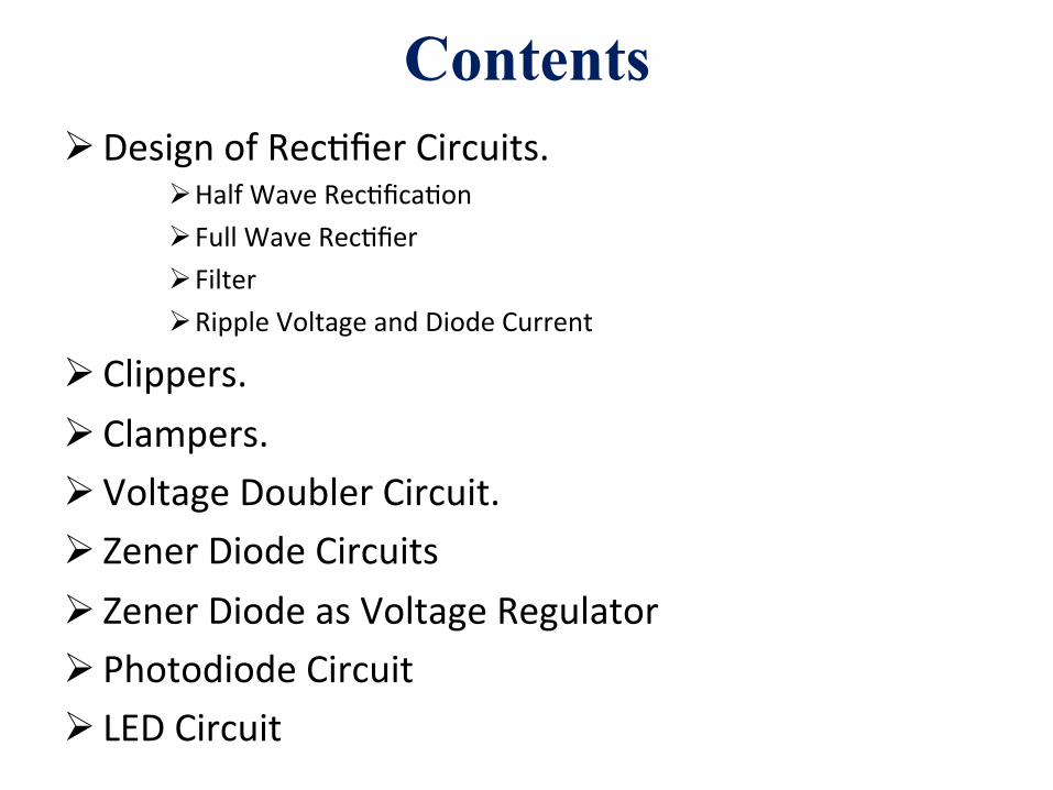
Contents Ø DesignofRec,fierCircuits.
Ø HalfWaveRec,fica,on
Ø FullWaveRec,fier
Ø FilterØ RippleVoltageandDiodeCurrent
Ø Clippers.Ø Clampers.
Ø VoltageDoublerCircuit.Ø ZenerDiodeCircuitsØ ZenerDiodeasVoltageRegulatorØ PhotodiodeCircuitØ LEDCircuit
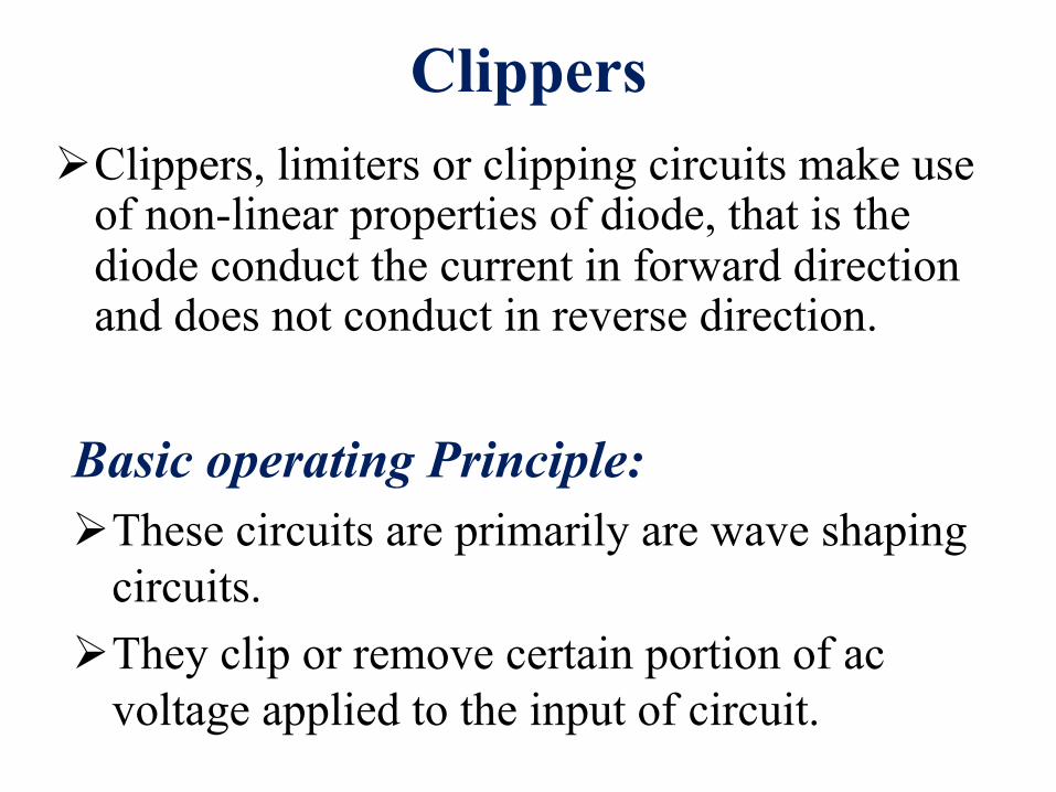
Clippers Ø Clippers, limiters or clipping circuits make use
of non-linear properties of diode, that is the diode conduct the current in forward direction and does not conduct in reverse direction.
Basic operating Principle: Ø These circuits are primarily are wave shaping
circuits. Ø They clip or remove certain portion of ac
voltage applied to the input of circuit.
Applications of Clippers: Ø They need to clip the voltage above or below a
certain pre-determined voltage level arises in the television, digital computers, radar, and many other electronic circuits.
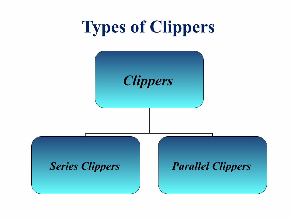
Types of Clippers
Clippers
Series Clippers Parallel Clippers
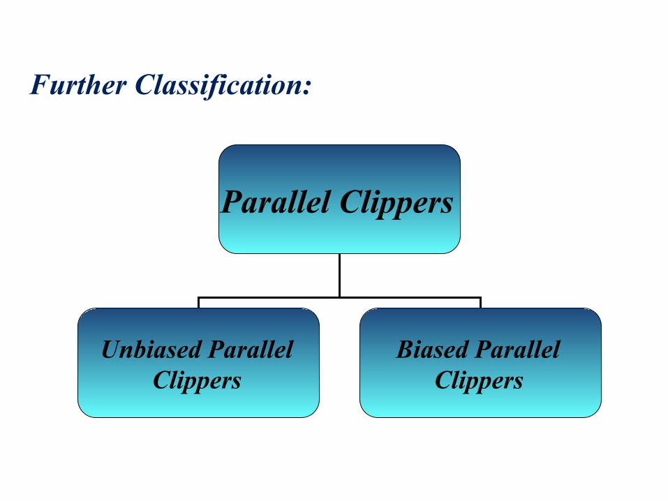
Further Classification:
Parallel Clippers
Unbiased Parallel Clippers
Biased Parallel Clippers
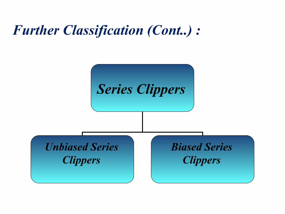
Further Classification (Cont..) :
Series Clippers
Unbiased Series Clippers
Biased Series Clippers
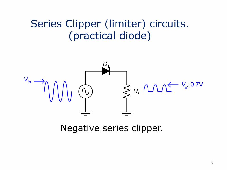
8
Series Clipper (limiter) circuits. (practical diode)
Negative series clipper.
D1
RL
Vin Vin-0.7V
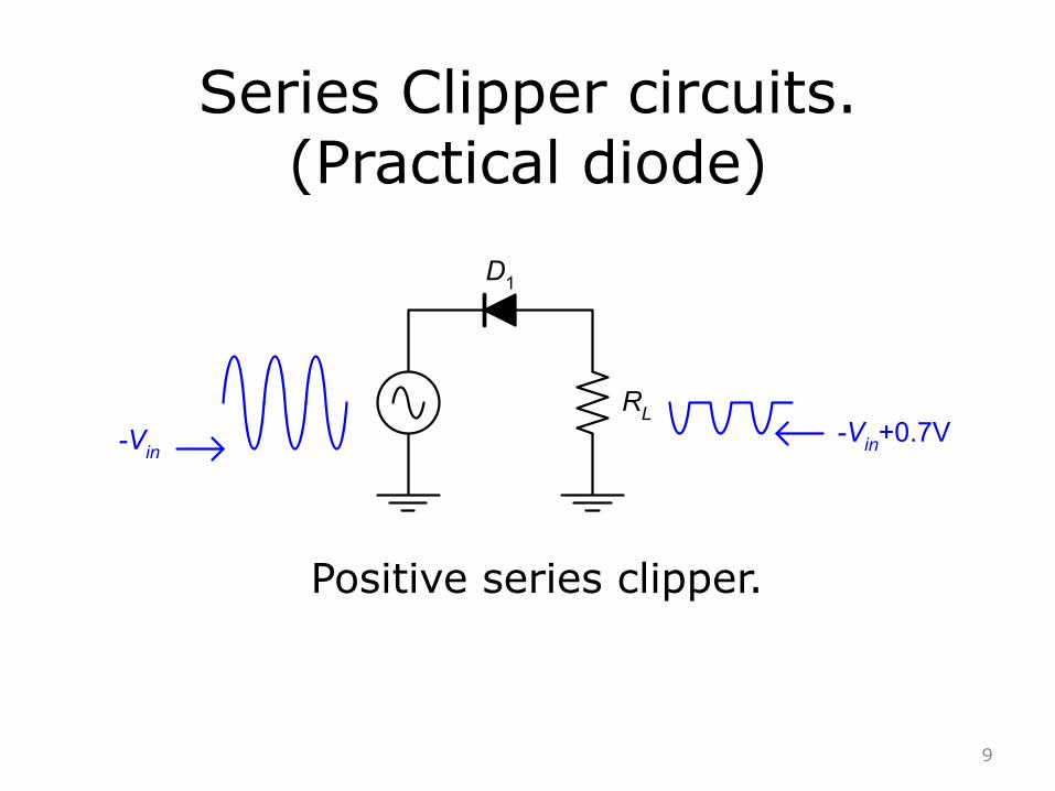
9
Series Clipper circuits. (Practical diode)
Positive series clipper.
D1
RL-Vin -Vin+0.7V
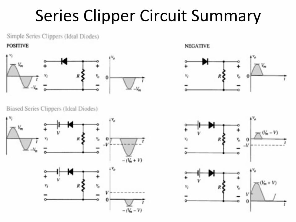
SeriesClipperCircuitSummary
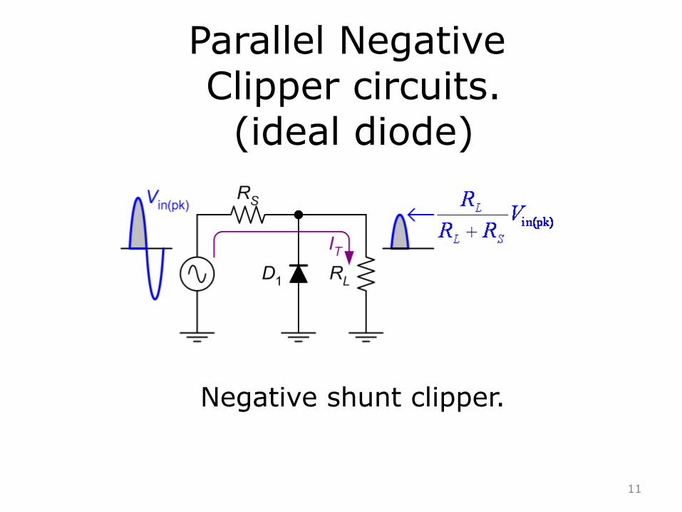
11
Parallel Negative Clipper circuits.
(ideal diode)
Negative shunt clipper.
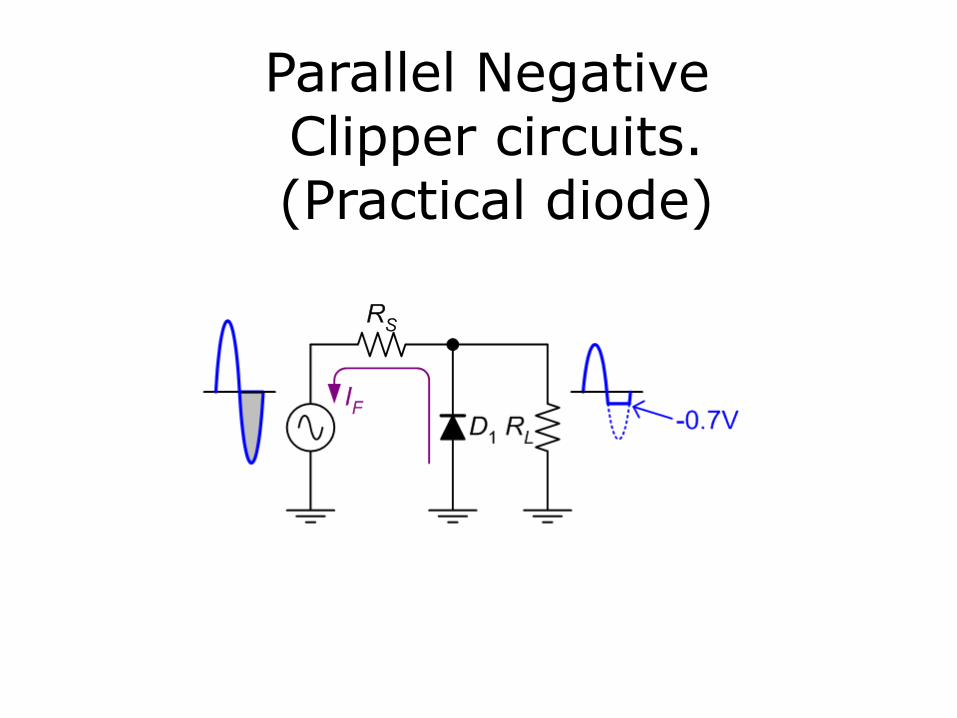
Parallel Negative Clipper circuits. (Practical diode)
13
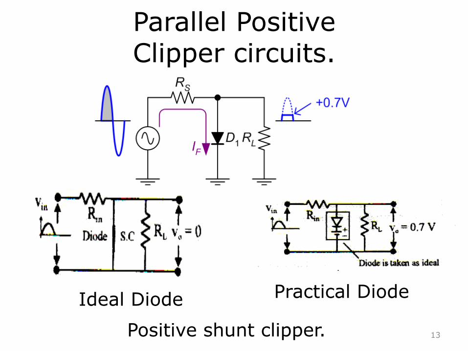
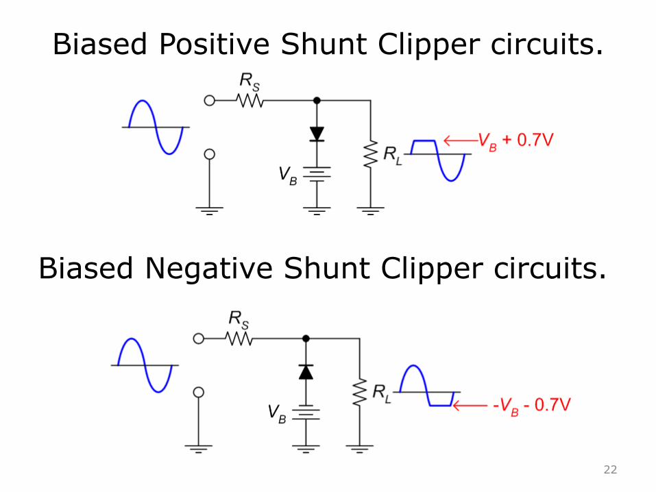
Parallel Positive Clipper circuits.
Positive shunt clipper. Ideal Diode Practical Diode
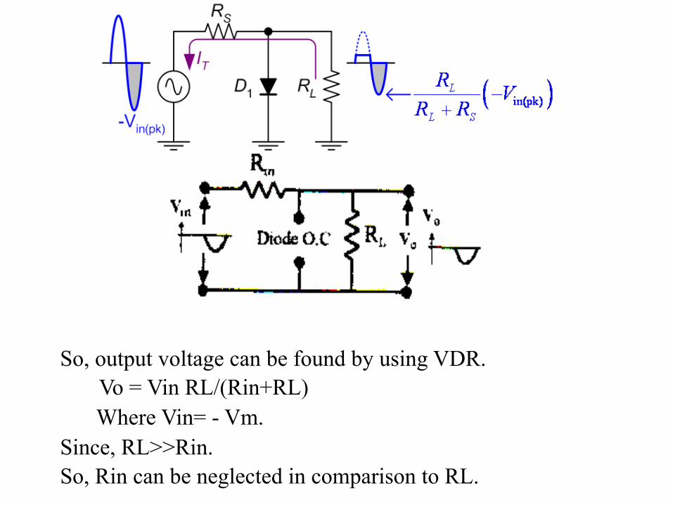
Ø So, output voltage can be found by using VDR. Ø Vo = Vin RL/(Rin+RL) Where Vin= - Vm. Ø Since, RL>>Rin. Ø So, Rin can be neglected in comparison to RL.
Biased parallel clipper
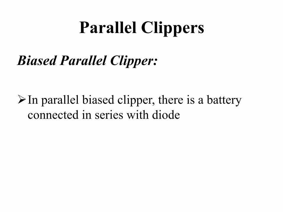
Parallel Clippers
Biased Parallel Clipper: Ø In parallel biased clipper, there is a battery
connected in series with diode

Parallel Positive Clippers
Analysis of biased parallel clipper: Ideal Diode:
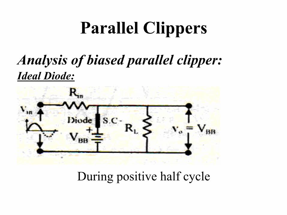
Parallel Clippers
Analysis of biased parallel clipper: Ideal Diode:
During positive half cycle
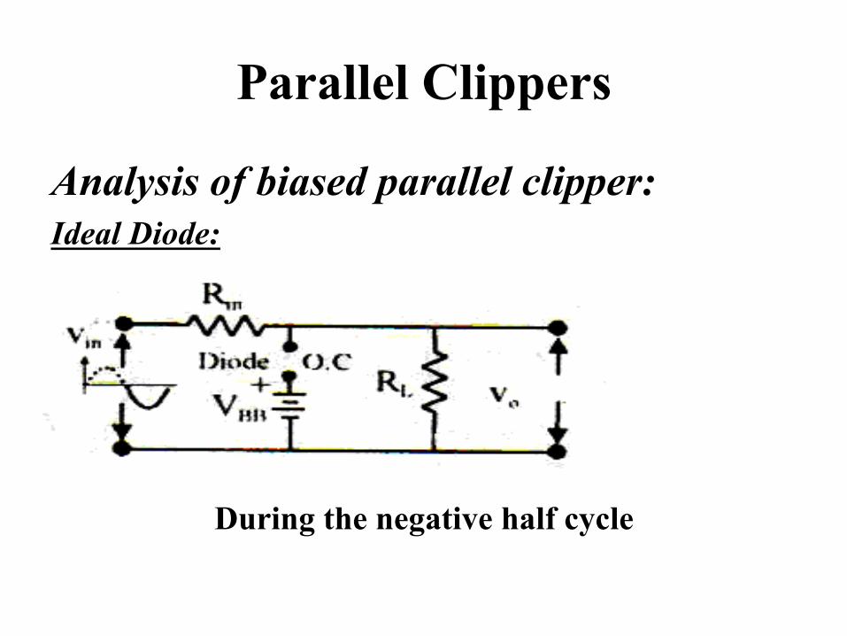
Parallel Clippers
Analysis of biased parallel clipper: Ideal Diode:
Output waveform during negative half cycle
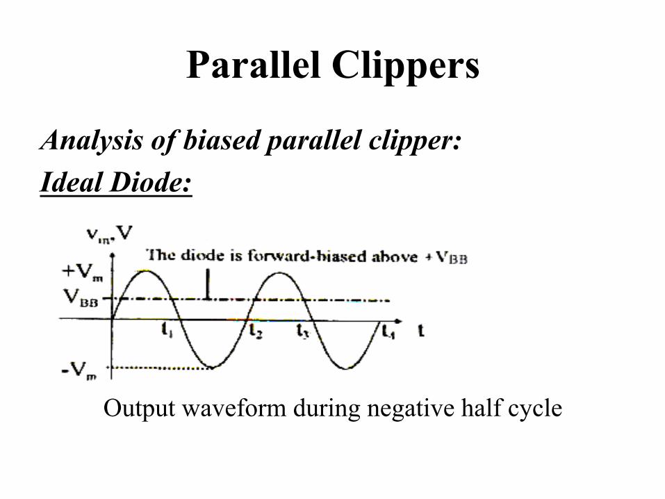
Parallel Clippers
Analysis of biased parallel clipper: Ideal Diode:
During the negative half cycle
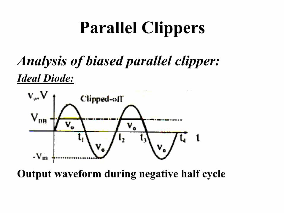
Parallel Clippers
Analysis of biased parallel clipper: Ideal Diode: Output waveform during negative half cycle
22
Biased Positive Shunt Clipper circuits.
Biased Negative Shunt Clipper circuits.

Design Problems
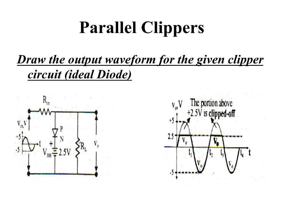
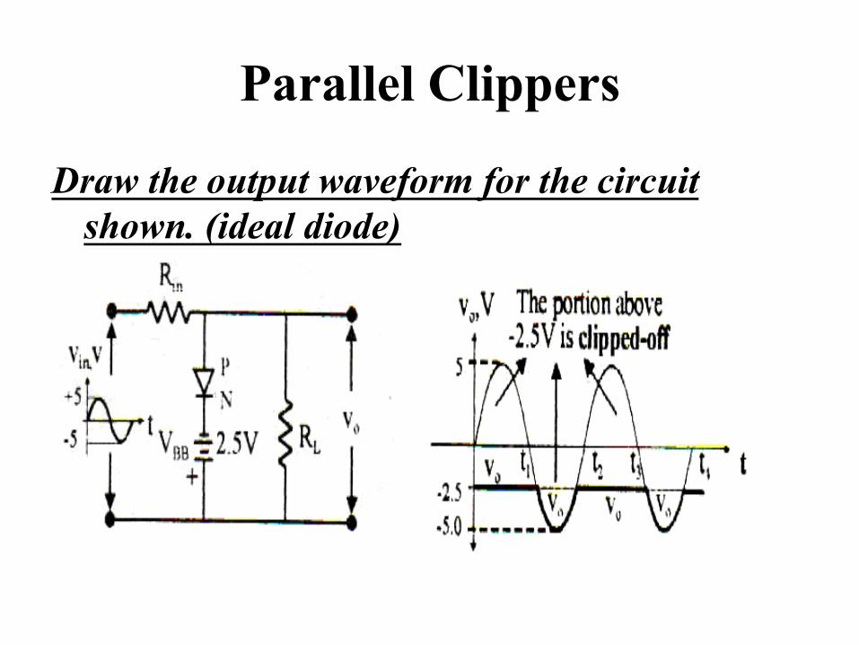
Parallel Clippers
Draw the output waveform for the given clipper circuit (ideal Diode)
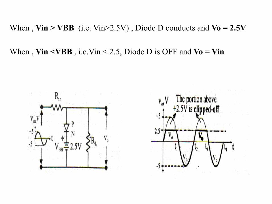
When , Vin > VBB (i.e. Vin>2.5V) , Diode D conducts and Vo = 2.5V When , Vin <VBB , i.e.Vin < 2.5, Diode D is OFF and Vo = Vin
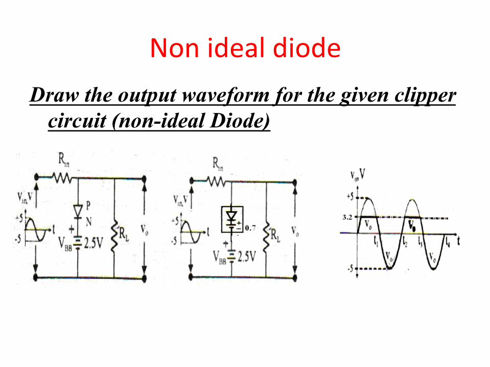
Nonidealdiode
Draw the output waveform for the given clipper circuit (non-ideal Diode)
Parallel Clippers
Draw the output waveform for the circuit shown. (ideal diode)
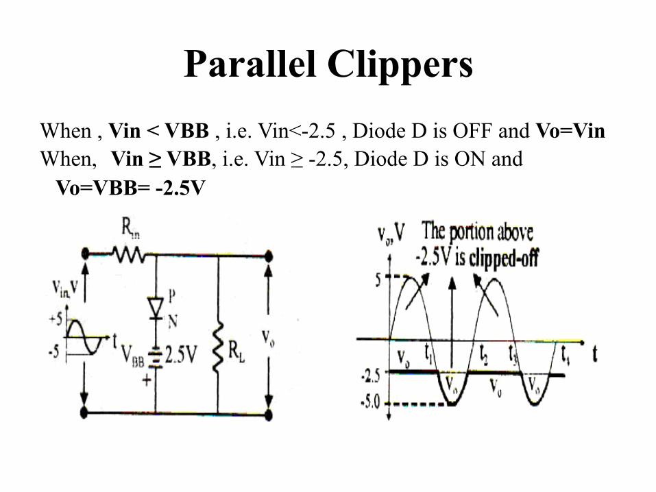
Parallel ClippersWhen , Vin < VBB , i.e. Vin<-2.5 , Diode D is OFF and Vo=Vin When, Vin ≥ VBB, i.e. Vin ≥ -2.5, Diode D is ON and Vo=VBB= -2.5V

Non-Idealdiode
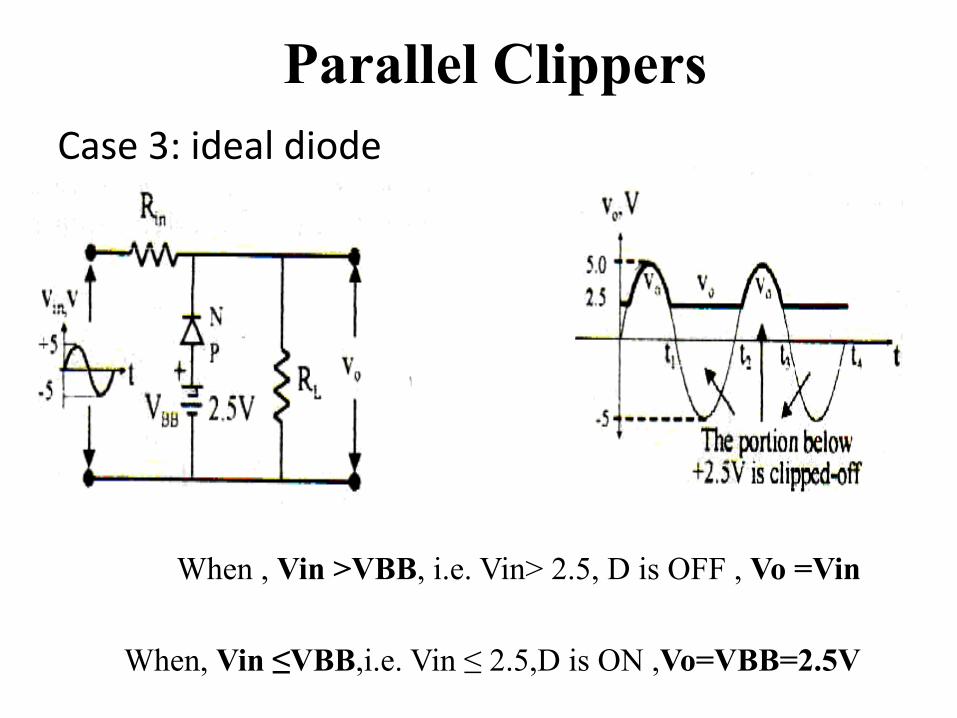
Parallel Clippers Case3:idealdiode
When , Vin >VBB, i.e. Vin> 2.5, D is OFF , Vo =Vin
When, Vin ≤VBB,i.e. Vin ≤ 2.5,D is ON ,Vo=VBB=2.5V

Nonidealdiode
Parallel Clippers
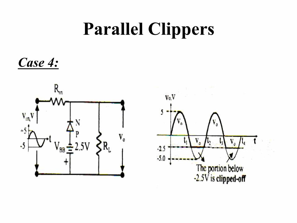
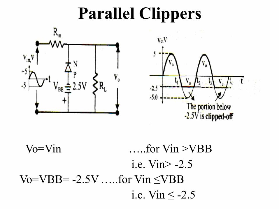
Case 4:
Parallel Clippers
Vo=Vin …..for Vin >VBB
i.e. Vin> -2.5 Vo=VBB= -2.5V …..for Vin ≤VBB
i.e. Vin ≤ -2.5
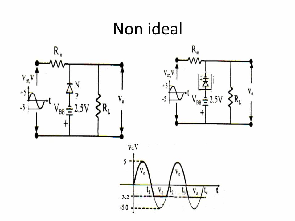
Nonideal
35
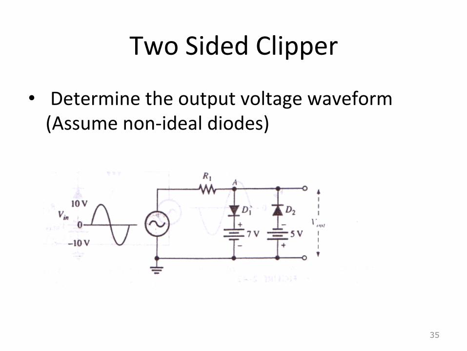
TwoSidedClipper
• Determinetheoutputvoltagewaveform(Assumenon-idealdiodes)
36
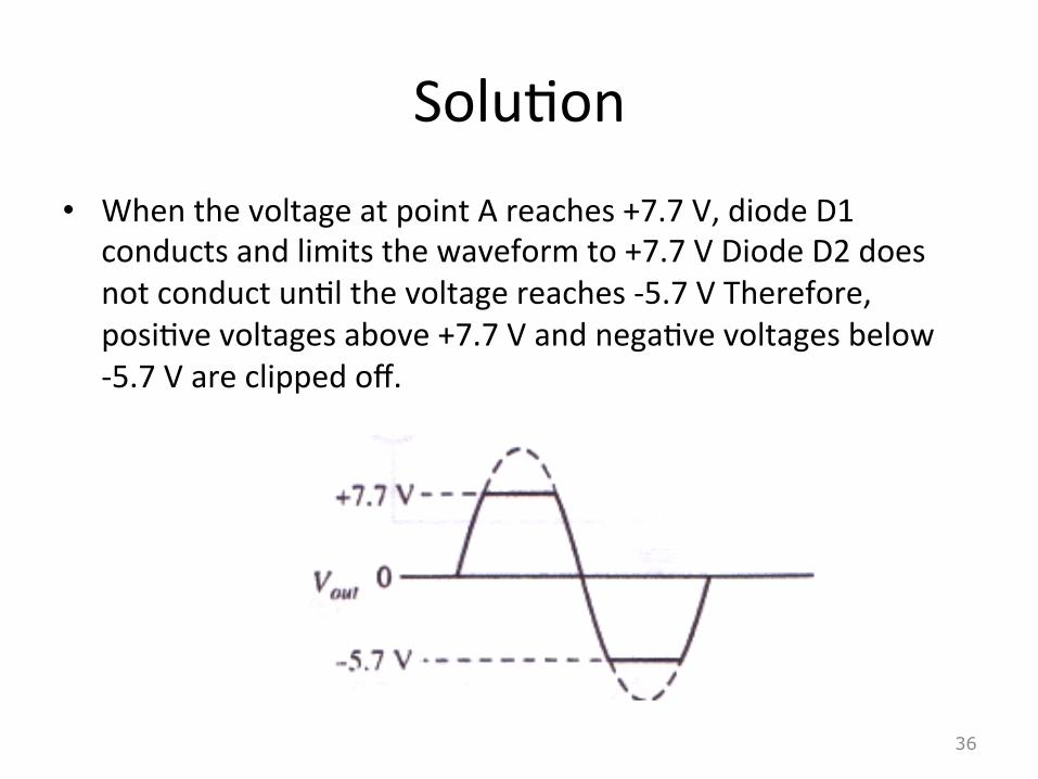
Solu,on
• WhenthevoltageatpointAreaches+7.7V,diodeD1conductsandlimitsthewaveformto+7.7VDiodeD2doesnotconductun,lthevoltagereaches-5.7VTherefore,posi,vevoltagesabove+7.7Vandnega,vevoltagesbelow-5.7Vareclippedoff.
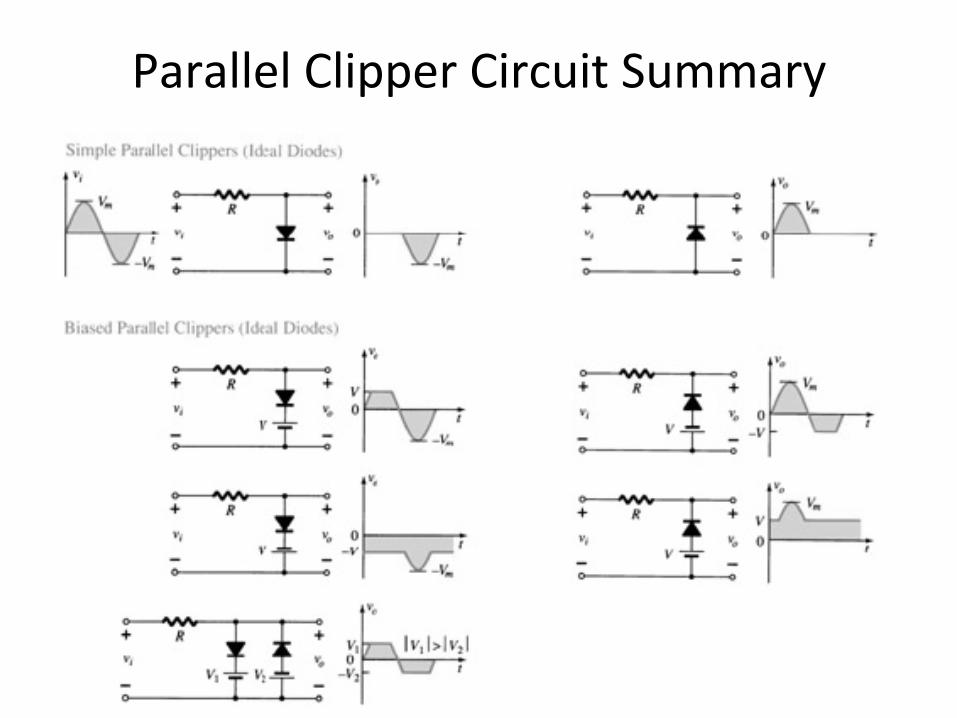
ParallelClipperCircuitSummary
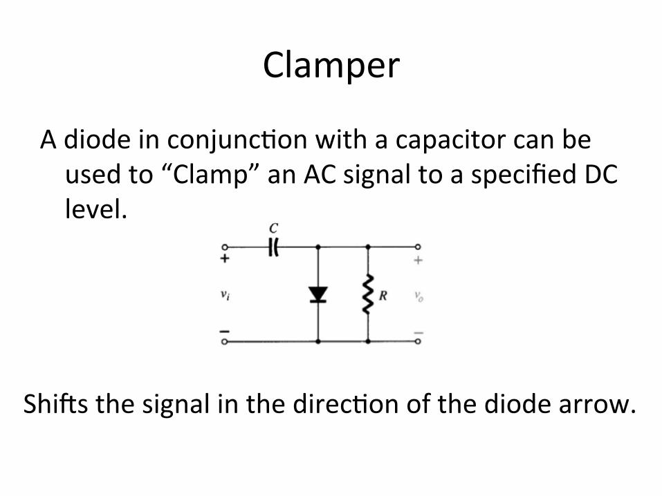
Clamper
Adiodeinconjunc,onwithacapacitorcanbeusedto“Clamp”anACsignaltoaspecifiedDClevel.
ShiYsthesignalinthedirec,onofthediodearrow.
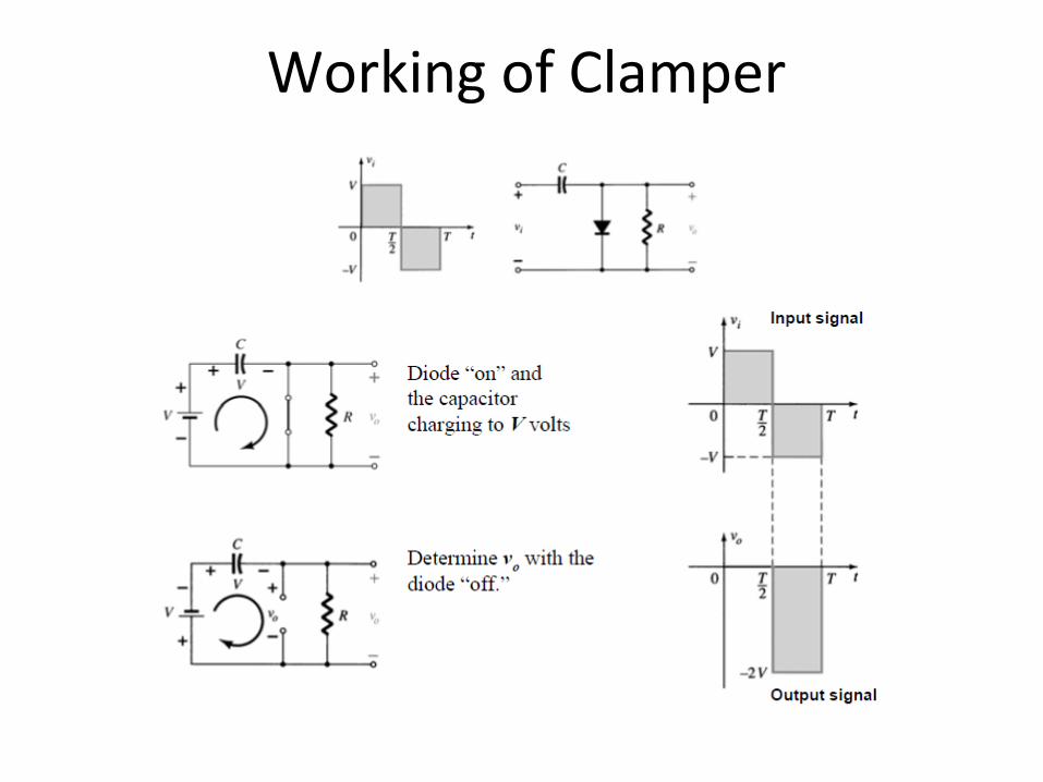
WorkingofClamper
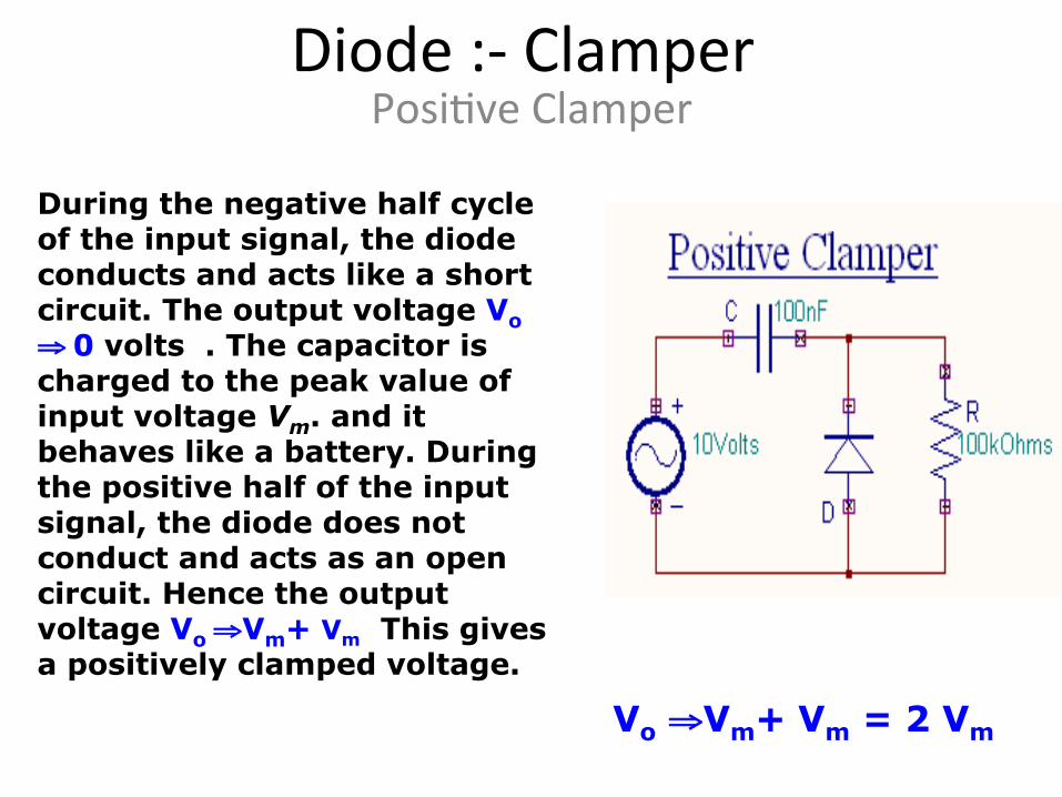
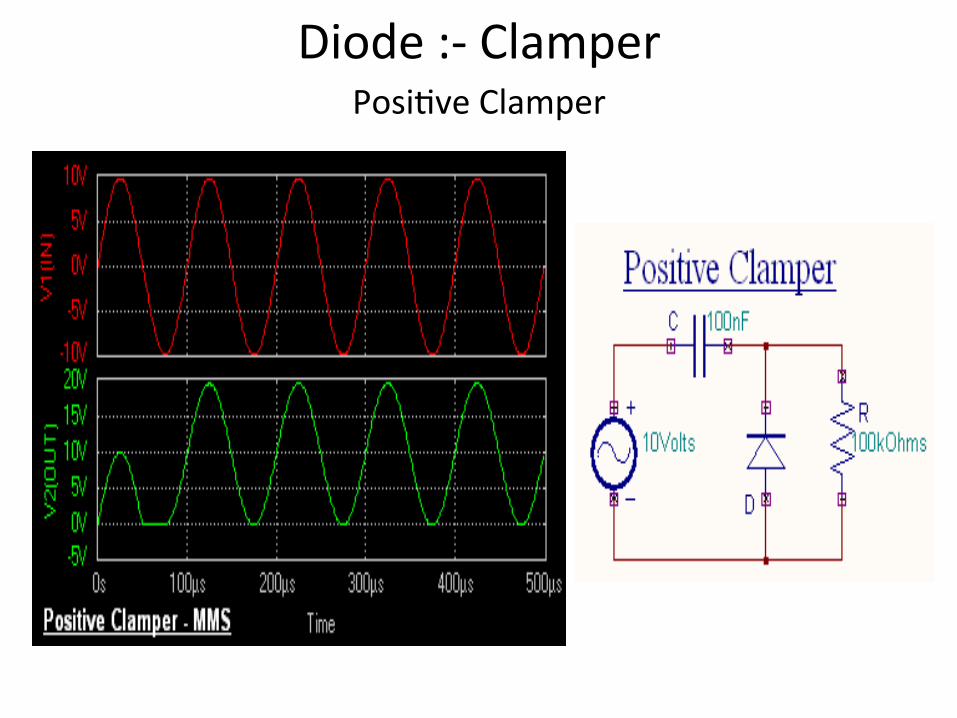
Diode:-ClamperPosi,veClamper
During the negative half cycle of the input signal, the diode conducts and acts like a short circuit. The output voltage Vo ⇒ 0 volts . The capacitor is charged to the peak value of input voltage Vm. and it behaves like a battery. During the positive half of the input signal, the diode does not conduct and acts as an open circuit. Hence the output voltage Vo ⇒Vm+ Vm This gives a positively clamped voltage.
Vo ⇒Vm+ Vm = 2 Vm
Diode:-ClamperPosi,veClamper
Diode:-ClamperNega,veClamper
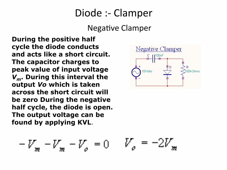
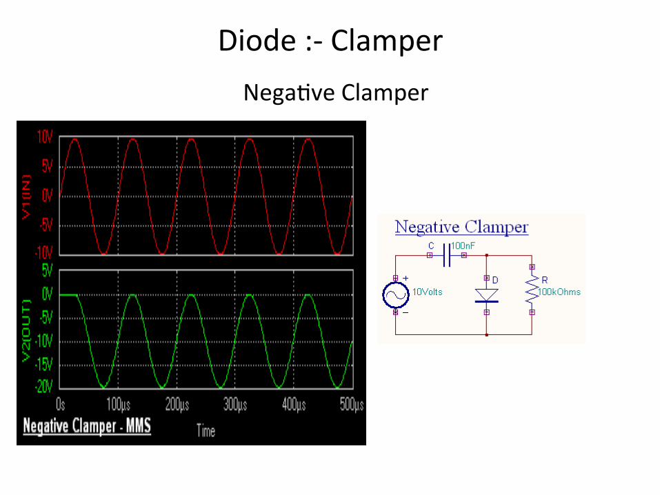
During the positive half cycle the diode conducts and acts like a short circuit. The capacitor charges to peak value of input voltage Vm. During this interval the output Vo which is taken across the short circuit will be zero During the negative half cycle, the diode is open. The output voltage can be found by applying KVL.
Diode:-Clamper
Nega,veClamper
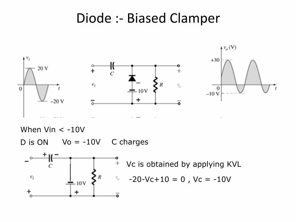
Diode:-BiasedClamperBiasedClamper
When Vin < -10V
D is ON Vo = -10V C charges
Vc is obtained by applying KVL
-20-Vc+10 = 0 , Vc = -10V
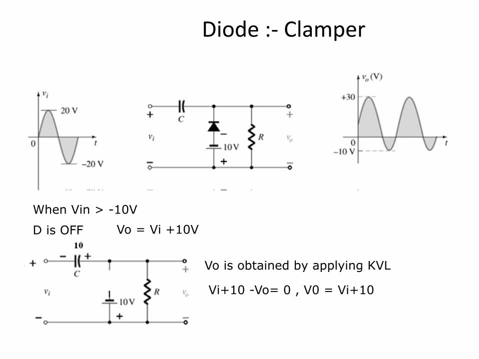
Diode:-ClamperBiasedClamper
When Vin > -10V
D is OFF Vo = Vi +10V
Vo is obtained by applying KVL
Vi+10 -Vo= 0 , V0 = Vi+10
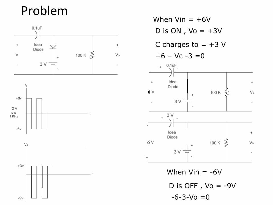
ProblemWhen Vin = +6V D is ON , Vo = +3V
C charges to = +3 V +6 – Vc -3 =0
When Vin = -6V
D is OFF , Vo = -9V -6-3-Vo =0

Problem When Vin = -20V D is ON , Vo = +5V
C charges to = -25 V -20-Vc-5=0
When Vin = +10V
D is OFF , Vo =35V 10+25-Vo=0
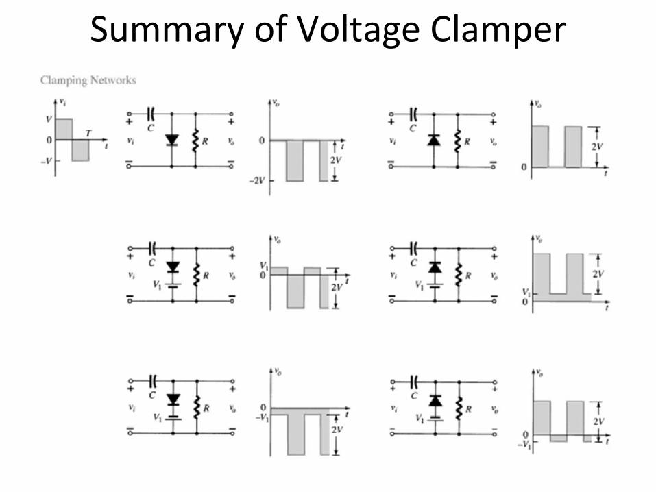
SummaryofVoltageClamper
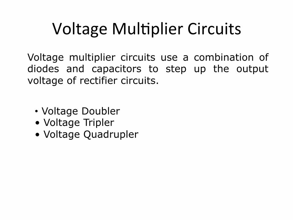
VoltageMul,plierCircuits
Voltage multiplier circuits use a combination of diodes and capacitors to step up the output voltage of rectifier circuits.
• Voltage Doubler • Voltage Tripler • Voltage Quadrupler
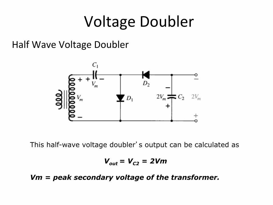
VoltageDoubler
This half-wave voltage doubler�s output can be calculated as
Vout = VC2 = 2Vm
Vm = peak secondary voltage of the transformer.
HalfWaveVoltageDoubler
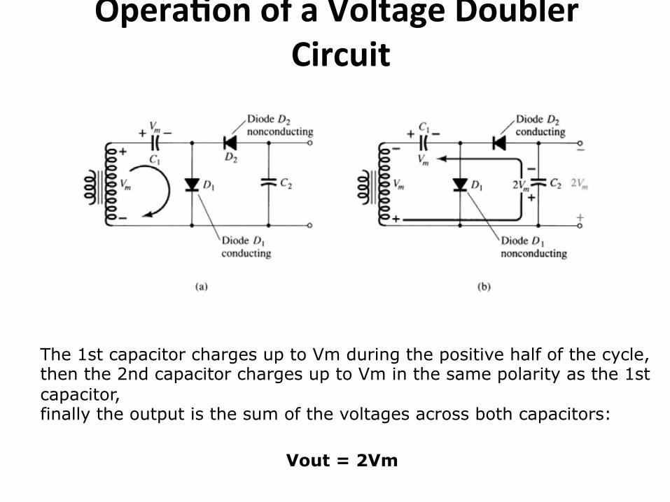
Opera'onofaVoltageDoublerCircuit
The 1st capacitor charges up to Vm during the positive half of the cycle, then the 2nd capacitor charges up to Vm in the same polarity as the 1st capacitor, finally the output is the sum of the voltages across both capacitors:
Vout = 2Vm
52
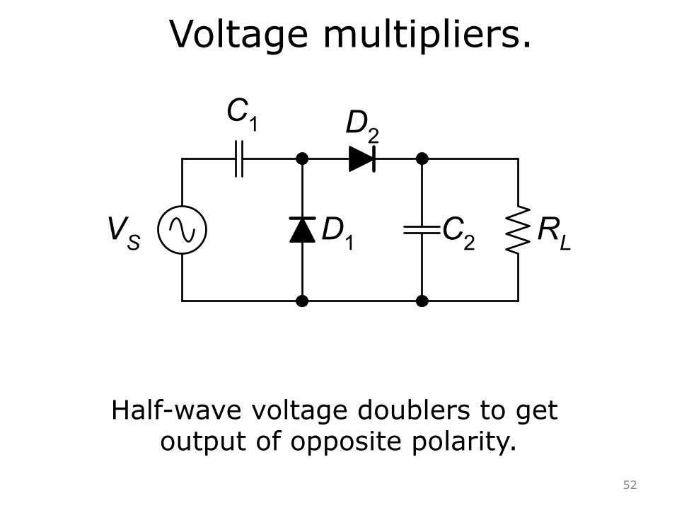
Voltage multipliers.
Half-wave voltage doublers to get output of opposite polarity.
VS
C1
D1
D2
C2 RL
53
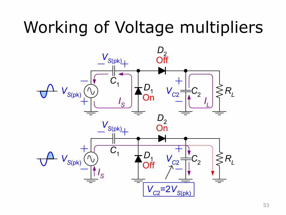
Working of Voltage multipliers
VS(pk)C1 D1
D2
C2 RLOn
Off
IS IL
VS(pk)
VC2
VS(pk)C1 D1
D2
C2 RLIS
Off
OnVS(pk)
VC2
VC2=2VS(pk)
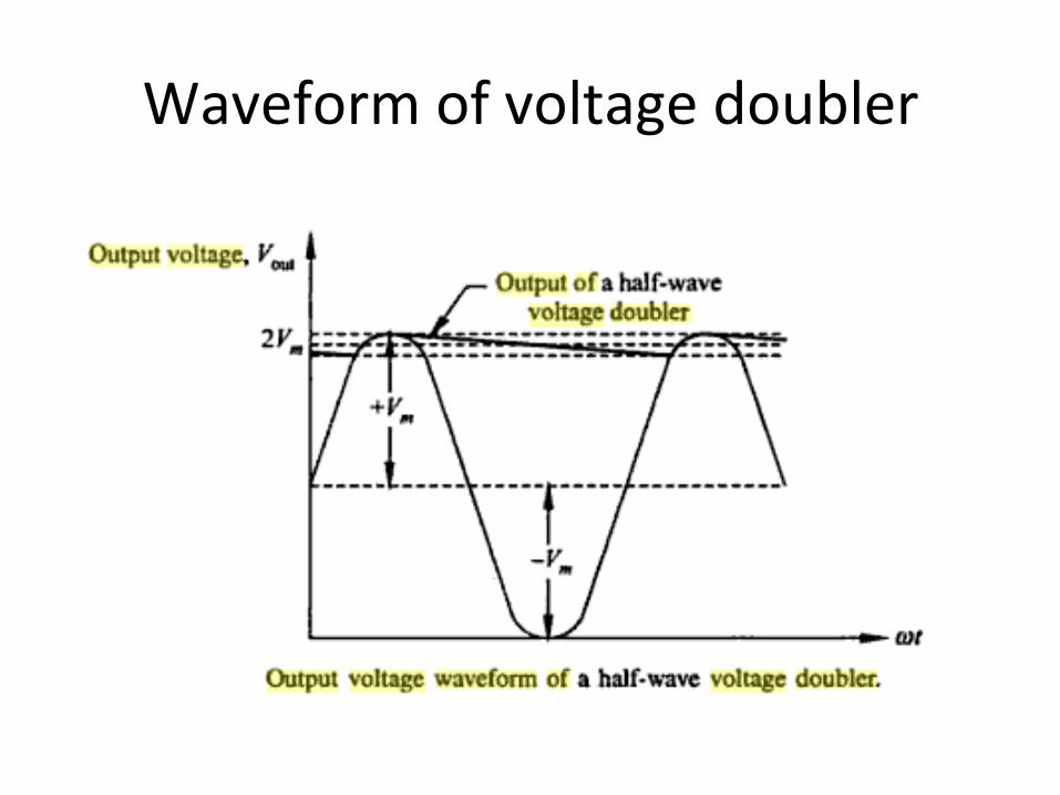
Waveformofvoltagedoubler
55
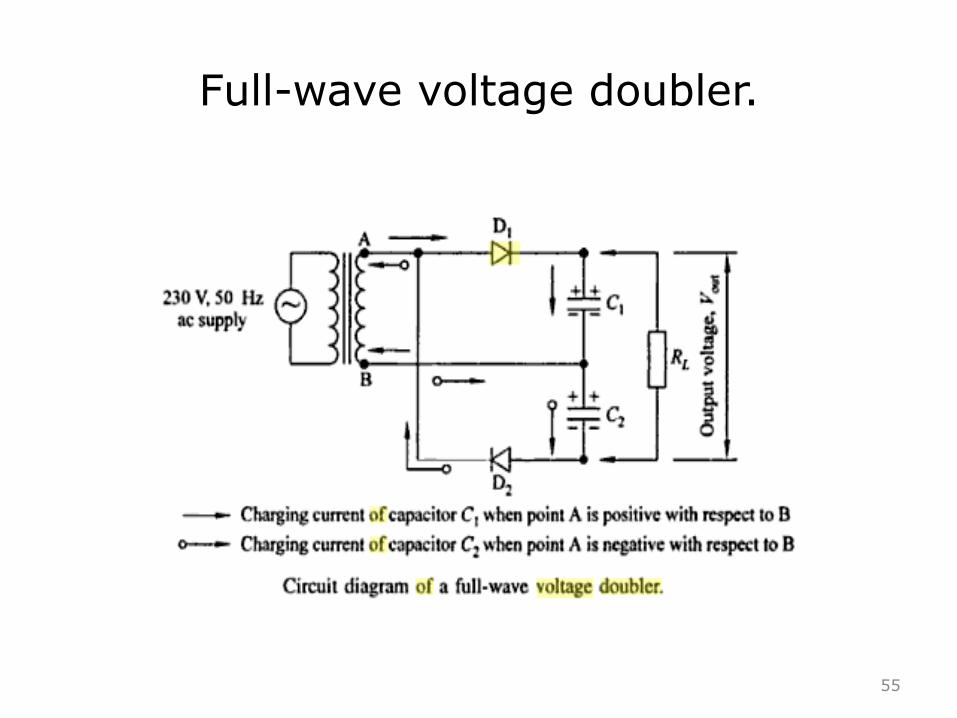
Full-wave voltage doubler.
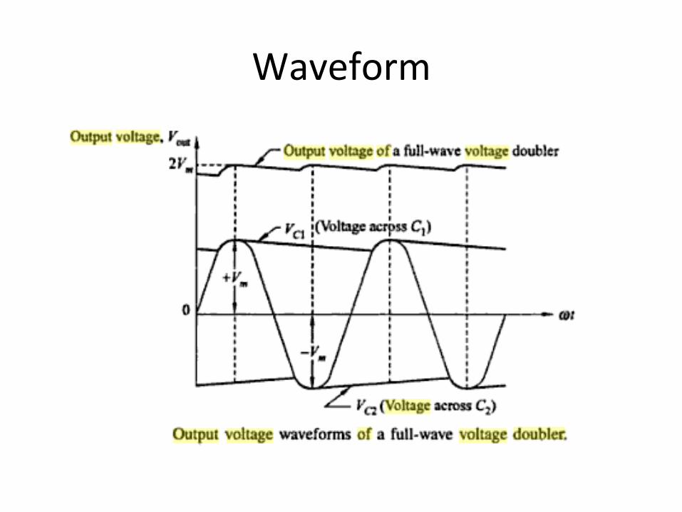
Waveform