Embed Size (px)
Citation preview

UPDATE ON STUDY OF WELDING POROSITY IN NB EBW
Y. Iwashita, Y. Fuwa, H. Tongu, Kyoto ICR, Uji, KyotoH. Hayano, KEK, Ibaraki
AbstractWe have been developing high-resolution inspection
systems and the connected instruments for SRF cavitydevelopments. They include the cavity camera – so-called Kyoto-Camera, eddy current scanner, high-densityT-map and X-map system and the local grinding system.They revealed an existence of voids beneath the surfaceof EBW seam. Study on the welding porosity in the NbEBW seams is reported.
INTRODUCTIONNondestructive Inspections have been playing
important roles on improving yield in production of highperformance SC Cavities. Starting from the high-resolution camera for inspection of the cavity innersurface, high resolution T-map, X-map and eddy currentscanner have been developed [1-7]. The positionidentification based on the inspection results enabled us tofix a defected cavity by the local repair technique.Throughout these processes, voids have been found in theNb EBW seams. Since the buried defects cannot beobserved by the optical inspections, other techniques haveto be applied to study their characteristics such asdistributions. X-ray or neutron radiography has been triedfor the purpose.
EXISTENCE OF VOIDFigure 1 shows the combined cavity camera and the
local grinding system. The camera cylinder and thegrinder cylinder can be switched quickly for the series ofinspection and repair process. Defects found on thesurface by the optical inspections have been effectivelyeliminated for many cases as shown in Figure 2. In spiteof this success, it has been found that new defectssometimes appear after the EP on a cavity repaired by thelocal grinding technique as shown in Figure 3. Theygrew with the local grindings: the further the grounddepth went, the bigger the pit size grew. This alludesthat they are voids buried beneath the surfaces. Thesevoids appeared again after the local grinding followed byEP process.
VOID INSPECTION EFFORTThus study on the welding porosity in the Nb EBW has
been found to be important to us in order to discard suchcavities at early stage in the production sequence. Sincethese voids cannot be observed by the optical inspectionsystem, other technique had to be developed. The eddy-current scanner is not easy to apply on the EBW seamsince it was developed for the inspections on the flat Nbsheets before the press. Another techniques areradiographies where X-rays or neutrons are used. SinceNb has larger atomic number Z=41 than iron (Z=26), X-
Figure 1: Combined cavity camera and local grindersystem. The cylinders can be switched for a cavity ininspect and repair cycles.
Figure 2: Succeeded example on the local grinding.
Figure 3: Voids appear after EP on the locally groundedcavity for repair.
Proceedings of SRF2013, Paris, France TUP061
04 Measurement techniques
H. Basic R&D bulk Nb - Other processing
ISBN 978-3-95450-143-4
567 Cop
yrig
htc ○
2013
byth
ere
spec
tive
auth
ors
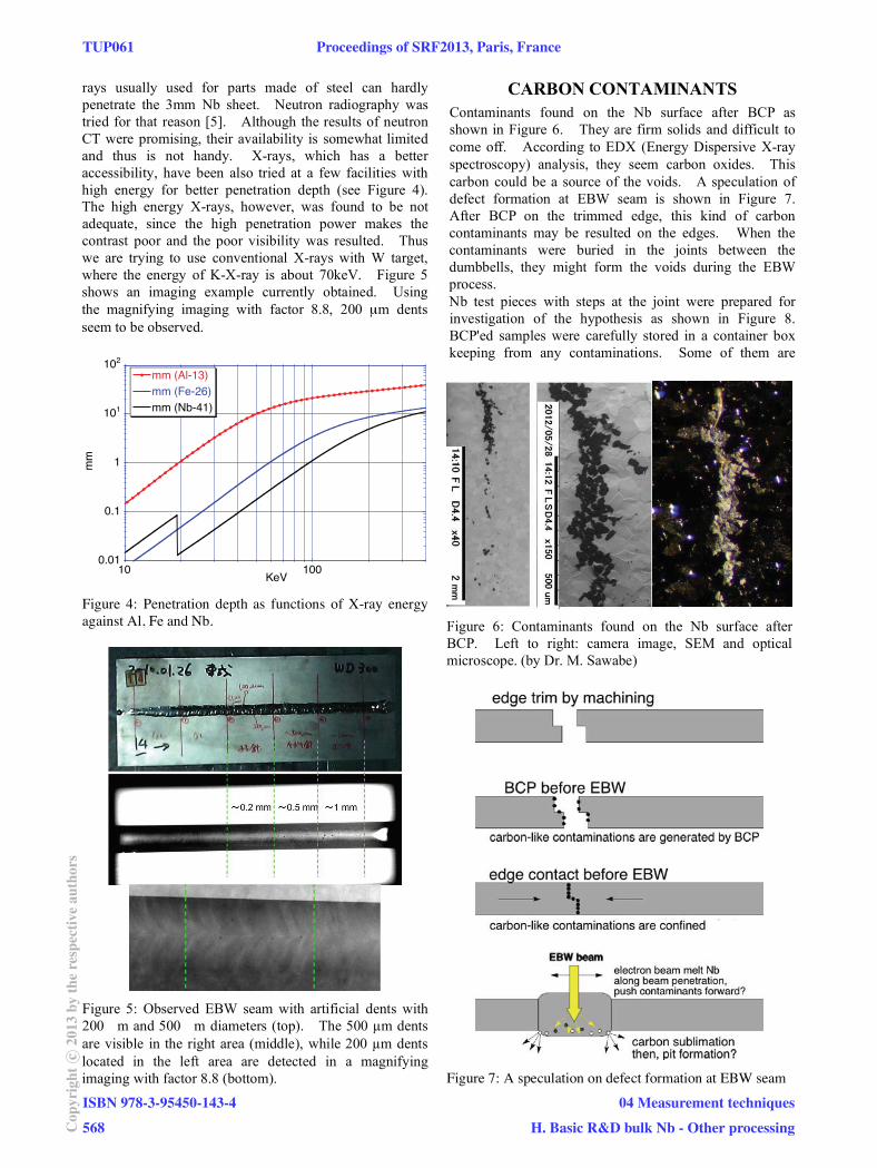
rays usually used for parts made of steel can hardlypenetrate the 3mm Nb sheet. Neutron radiography wastried for that reason [5]. Although the results of neutronCT were promising, their availability is somewhat limitedand thus is not handy. X-rays, which has a betteraccessibility, have been also tried at a few facilities withhigh energy for better penetration depth (see Figure 4).The high energy X-rays, however, was found to be notadequate, since the high penetration power makes thecontrast poor and the poor visibility was resulted. Thuswe are trying to use conventional X-rays with W target,where the energy of K-X-ray is about 70keV. Figure 5shows an imaging example currently obtained. Usingthe magnifying imaging with factor 8.8, 200 m dentsseem to be observed.
0.01
0.1
1
101
102
10 100
mm (Al-13)mm (Fe-26)mm (Nb-41)
mm
KeV
Figure 4: Penetration depth as functions of X-ray energyagainst Al, Fe and Nb.
Figure 5: Observed EBW seam with artificial dents with200 m and 500 m diameters (top). The 500 μm dentsare visible in the right area (middle), while 200 located in the left area are detected in a magnifyingimaging with factor 8.8 (bottom).
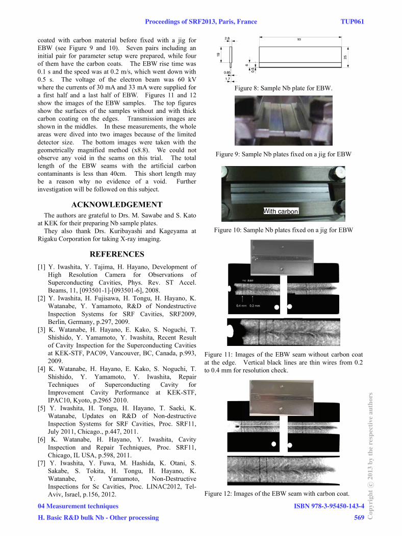
CARBON CONTAMINANTSContaminants found on the Nb surface after BCP asshown in Figure 6. They are firm solids and difficult tocome off. According to EDX (Energy Dispersive X-rayspectroscopy) analysis, they seem carbon oxides. Thiscarbon could be a source of the voids. A speculation ofdefect formation at EBW seam is shown in Figure 7.After BCP on the trimmed edge, this kind of carboncontaminants may be resulted on the edges. When thecontaminants were buried in the joints between thedumbbells, they might form the voids during the EBWprocess. Nb test pieces with steps at the joint were prepared forinvestigation of the hypothesis as shown in Figure 8.BCP'ed samples were carefully stored in a container boxkeeping from any contaminations. Some of them are
Figure 6: Contaminants found on the Nb surface afterBCP. Left to right: camera image, SEM and opticalmicroscope. (by Dr. M. Sawabe)
Figure 7: A speculation on defect formation at EBW seam
μm dents
TUP061 Proceedings of SRF2013, Paris, France
ISBN 978-3-95450-143-4
568Cop
yrig
htc ○
2013
byth
ere
spec
tive
auth
ors
04 Measurement techniques
H. Basic R&D bulk Nb - Other processing
coated with carbon material before fixed with a jig forEBW (see Figure 9 and 10). Seven pairs including aninitial pair for parameter setup were prepared, while fourof them have the carbon coats. The EBW rise time was0.1 s and the speed was at 0.2 m/s, which went down with0.5 s. The voltage of the electron beam was 60 kVwhere the currents of 30 mA and 33 mA were supplied fora first half and a last half of EBW. Figures 11 and 12show the images of the EBW samples. The top figuresshow the surfaces of the samples without and with thickcarbon coating on the edges. Transmission images areshown in the middles. In these measurements, the wholeareas were dived into two images because of the limiteddetector size. The bottom images were taken with thegeometrically magnified method (x8.8). We could notobserve any void in the seams on this trial. The totallength of the EBW seams with the artificial carboncontaminants is less than 40cm. This short length maybe a reason why no evidence of a void. Furtherinvestigation will be followed on this subject.
ACKNOWLEDGEMENTThe authors are grateful to Drs. M. Sawabe and S. Kato
at KEK for their preparing Nb sample plates.They also thank Drs. Kuribayashi and Kageyama at
Rigaku Corporation for taking X-ray imaging.
REFERENCES
[1] Y. Iwashita, Y. Tajima, H. Hayano, Development ofHigh Resolution Camera for Observations ofSuperconducting Cavities, Phys. Rev. ST Accel.Beams, 11, [093501-1]-[093501-6], 2008.
[2] Y. Iwashita, H. Fujisawa, H. Tongu, H. Hayano, K.Watanabe, Y. Yamamoto, R&D of NondestructiveInspection Systems for SRF Cavities, SRF2009,Berlin, Germany, p.297, 2009.
[3] K. Watanabe, H. Hayano, E. Kako, S. Noguchi, T.Shishido, Y. Yamamoto, Y. Iwashita, Recent Resultof Cavity Inspection for the Superconducting Cavitiesat KEK-STF, PAC09, Vancouver, BC, Canada, p.993,2009.
[4] K. Watanabe, H. Hayano, E. Kako, S. Noguchi, T.Shishido, Y. Yamamoto, Y. Iwashita, RepairTechniques of Superconducting Cavity forImprovement Cavity Performance at KEK-STF,IPAC10, Kyoto, p.2965 2010.
[5] Y. Iwashita, H. Tongu, H. Hayano, T. Saeki, K.Watanabe, Updates on R&D of Non-destructiveInspection Systems for SRF Cavities, Proc. SRF11,July 2011, Chicago., p.447, 2011.
[6] K. Watanabe, H. Hayano, Y. Iwashita, CavityInspection and Repair Techniques, Proc. SRF11,Chicago, IL USA, p.598, 2011.
[7] Y. Iwashita, Y. Fuwa, M. Hashida, K. Otani, S.Sakabe, S. Tokita, H. Tongu, H. Hayano, K.Watanabe, Y. Yamamoto, Non-DestructiveInspections for Sc Cavities, Proc. LINAC2012, Tel-Aviv, Israel, p.156, 2012.
Figure 8: Sample Nb plate for EBW.
Figure 9: Sample Nb plates fixed on a jig for EBW
Figure 10: Sample Nb plates fixed on a jig for EBW
Figure 11: Images of the EBW seam without carbon coatat the edge. Vertical black lines are thin wires from 0.2to 0.4 mm for resolution check.
Figure 12: Images of the EBW seam with carbon coat.
Proceedings of SRF2013, Paris, France TUP061
04 Measurement techniques
H. Basic R&D bulk Nb - Other processing
ISBN 978-3-95450-143-4
569 Cop
yrig
htc ○
2013
byth
ere
spec
tive
auth
ors