Embed Size (px)
Citation preview

111111111111111111111111111111111111111111111111111111111111111111111111
(12) United States PatentSumant et al.
(54) PLANAR FIELD EMITTERS AND HIGHEFFICIENCY PHOTOCATHODES BASED ONULTRANANOCRYSTALLINE DIAMOND
(71) Applicant: UChicago Argonne, LLC, Chicago, IL(US)
(72) Inventors: Anirudha V. Sumant, Plainfield, IL(US); Sergey V. Baryshev, Lemont, IL(US); Sergey P. Antipov, Naperville, IL(US)
(73) Assignee: UCHICAGO ARGONNE, LLC,Chicago, IL (US)
(*) Notice: Subject to any disclaimer, the term of thispatent is extended or adjusted under 35U.S.C. 154(b) by 0 days.
(21) Appl. No.: 14/594,949
(22) Filed: Jan. 12, 2015
(65) Prior Publication Data
US 2016/0203937 Al Jul. 14, 2016
(51) Int. Cl.COIB 31/06 (2006.01)HOIJ11304 (2006.01)HOIJ9/02 (2006.01)HOIJ9/12 (2006.01)HOIJ1134 (2006.01)
(52) U.S. Cl.CPC . HOIJI/304 (2013.01); HOIJI/34 (2013.01);
HOIJ9/025 (2013.01); HOIJ9/12 (2013.01);HOIJ2201130457 (2013.01); HOIJ220113421
(2013.01)(58) Field of Classification Search
CPC ............. HO1J 1/304; HO1J 9/025; HO1J 9/12;HO1J 1/34
USPC .......................................................... 438/105See application file for complete search history.
(io) Patent No.: US 9,418,814 B2(45) Date of Patent: Aug. 16, 2016
(56) References Cited
U.S. PATENT DOCUMENTS
7,556,982 132 * 7/2009 Carlisle ................. C23C 16/274438/105
9,108,888 132 * 8/2015 Neogi ................... C04B 41/0092002/0041154 Al 4/2002 Tomasetti et al.2003/0001498 Al 1/2003 Niigaki et al.2006/0131588 Al* 6/2006 Gruen ................... C23C 16/274
257/772007/0220959 Al* 9/2007 Sumant .................. B 82 35/00
73/1052010/0051964 Al* 3/2010 Lin ..................... HO1L 29/1602
257/77
(Continued)
OTHER PUBLICATIONS
Baryshev, et al., "Planar ultrananocrystalline diamond field emitter inaccelerator radio frequency electron injector: Performance metrics,"Applied Physics Letters, vol. 105, No. 203505 (2014), pp. 203505-1-203505-5.
(Continued)
Primary Examiner Tracie Y Green(74) Attorney, Agent, or Firm Foley & Lardner LLP
(57) ABSTRACT
A method of forming a field emitter comprises disposing afirst layer on a substrate. The first layer is seeded with nano-diamond particles. The substrate with the first layer disposedthereon is maintained at a first temperature and a first pressurein a mixture of gases which includes nitrogen. The first layeris exposed to a microwave plasma to form a nitrogen dopedultrananocrystalline diamond film on the first layer, whichhas a percentage of nitrogen in the range of about 0.05 atom% to about 0.5 atom %. The field emitter has about 1012 toabout 1014 emitting sites per cm2. A photocathode can also beformed similarly by forming a nitrogen doped ultrananocrys-talline diamond film on a substrate similar to the field emitter,and then hydrogen terminating the film. The photocathode isresponsive to near ultraviolet light as well as to visible light.
29 Claims, 15 Drawing Sheets
https://ntrs.nasa.gov/search.jsp?R=20160011054 2018-08-21T09:51:17+00:00Z
US 9,418,814 B2Page 2
(56) References Cited
U.S. PATENT DOCUMENTS
2010/0052112 Al 3/2010 Rogers et al.2013/0082241 Al 4/2013 Kub et al.2013/0145857 Al 6/2013 Bryant et al.2013/0320295 Al 12/2013 Rao et al.2013/0333094 Al 12/2013 Rogers et al.
OTHER PUBLICATIONS
Grimes, Jacob T., "A Prototype Diamond Amplified Photocathode",
Master of Science Thesis, Stony Brook University, May 2007, pp.
ii-102.
Perez, et al., "High quantum efficiency ultrananocrystal line diamondphotocathode for photoinjector applications," Applied Physics Let-ters, vol. 105 (2014) pp. 123103-1-123103-4.
Rameau, et al., "Properties of Hydrogen Terminated Diamond as aPhotocathode", Physical Review Letters, Abstract, vol. 106, Issue137602,(Mar. 30, 2011), 4 pages.Sumant,et al., "High Quantum Efficiency Photocathodes Based onUltrananocrystal line Diamond Operating Between 250 nm and Vis-ible Blue", Slide Presentation, by Argonne and U.S. Department ofEnergy, Nov. 24, 2014,p. 1-7.Tremsin & Siegmund, "Polycrystalline diamond films as prospectiveUV photocathodes," Proceedings SPIE, vol. 4139, (2000), pp. 1-9.Gaowei, Responsive Study of Diamond X-Ray Monitors withnUNCD Contact Proc. of IPAC 2015, Jun. 2015, pp. 1273-1275.Ex Parte Quayle Action for U.S. Appl. No. 14/601,908, mailed Mar.30, 2016, 9 pages.Notice of Allowance on U.S. Appl. No. 14/601908, mailed May 9,2016, 7 pages.Notice of Allowance for U.S. Appl. No. 14/790,995, mailed Jun. 24,2016, 12 pages.
* cited by examiner

U.S. Patent Aug. 16, 2016 Sheet 1 of 15 US 9,418,814 B2
Ir
100
Substrate
Dispose a first layer on the substrate
Seed the first layer with nanodiamond (ND) particles
Maintain the substrate with the first layer disposed thereon at a firsttemperature and a first pressure in a mixture of gases that include
nitrogen
Expose the first layer to a microwave, plasma to form a N-UNCD film onthe first Dyer
102
04
100
M

U.S. Patent Aug. 16, 2016 Sheet 2 of 15 US 9,418,814 B2
230
FICA. 2
200
220
210
U.S. Patent Aug. 16, 2016 Sheet 3 of 15 US 9,418,814 B2

alCV,
1'0
G 1100 1200 1300 1400 1500 1600 1700 1800 1900 2000
1
venumber (CM
-)
i
U.S. Patent Aug. 16, 2016 Sheet 5 of 15 US 9,418,814 B2

U.S. Patent Aug. 16, 2016 Sheet 6 of 15 US 9,418,814 B2
EI-I ] 0
0

U.S. Patent Aug. 16, 2016 Sheet 7 of 15 US 9,418,814 B2
i
120
Total Charge detected b FC
planar
€ ...
g.
Cu
100
90B)
Emission
e i&
'darkcurrent ea
rn ~~~ ~d~s
~
110
100
(N)UNGD cathode - Fig
,3b
70
.a.o
'70
CL0
0
o£
60
CL
LL
0a
M 40
~0 40
UL
0
p
€~CU
f ~
3 020-00010
apt
r....a., a
00
w36
40 44 4
52
56 60 640
O.6
0,8
1.0
12
1A
lk
1 A
E field M /M
Inpu
t RF pow
er (MW)

FIG. 9
2:5
A~

m 0.1 .n
Electron Kin
etic
Energy Me
U.S. Patent Aug. 16, 2016 Sheet 11 of 15 US 9,418,814 B2
300
Substrate
Dispose a first layer on the substrate
Seed the first layer with nanodiamond (ND) particles
Maintain the substrate with the first layer disposed thereon at a firsttemperature and a first pressure in a mixture of gases that include
Expose the first layer to a first microwave plasma to form a N-U ADD Ifilm can the first layer
Maintain the N-UNCD film at a second temperature and secondpressure in hydrogen gas
Expose the N-UNCD film to a second microwave plasma to hydrogenterminate the N-UNCD film
FIG. 11
006
10
2

U.S. Patent Aug. 16, 2016 Sheet 12 of 15 US 9,418,814 B2
400
430
420
410
U.S. Patent Aug. 16, 2016 Sheet 13 of 15 US 9,418,814 B2
RWW $ W,
photocathode

FIG. 14
5,0-
4.8-
Polycrystalline Cu
4. 4.4
4.2
'4.
ON o
(N)UNCD
.f`
N)UNCD:H
10
.~/'i'X~"\~..:.+.\+V"wF4r•..'MW"R-:..v_~..:̂
Y'Y... by ..y~.~1! :.~/}.x'\.f4~.•\..1+`\w'~....i+s`Uv \.~1~f .M
:r
..
N"
"~
/.
.✓
V~.
':.
Yx` ff.+v,'1.'Y'..Wf^'1.~~
v,
btV
2, 2,4
2./2
2,0
Vl
0
20
40
60
80
100
120
140
160
`O
Time s
00

M 1€3'
102
1O3
CL 1
074
1(76
2
1t~6
10-
7
w le
107
1,
10-
10 240
CD
0 (N)
UNCC
D( )UNCCD:H
(N)UNCD:H
yOE ran
ge of
X Co.Te@ANL,
quaaI
kali
s fam
ily
r~KBr/Cu(100) PNNL
o
Poly-Cu holder
N
Cu(100)
PNNL.
° Cu@SwissFEL
a~
QE rang@ of
;
°~
Cu fa
mily
•9 a
O
r 4O 0
♦O~
8
280 280 300 320 340 380 380 400 420 440 460
~
Wavelength nm
N

US 9,418,814 B2
PLANAR FIELD EMITTERS AND HIGHEFFICIENCY PHOTOCATHODES BASED ONULTRANANOCRYSTALLINE DIAMOND
This invention was made with government support in partunder "Experimental Program to Stimulate CompetitiveResearch (EPSCoR)" Program Award NumberNNXI3AB222A awarded by the National Aeronautical andSpace Administration (NASA), under "Space Grant' Pro-gram Award Number NNXI0AM80H awarded by NASA,and under "Small Business Innovation Research (SBIR)"Program Award Number DE-SC0009572 by the Departmentof Energy (DOE). The United States Government claimscertain rights in this invention pursuant to Contract No. W-31-109-ENG-38 between the United States Government and theUniversity of Chicago and/or pursuant to DE-ACO2-06CH11357 between the United States Government andUChicago Argonne, LLC representing Argonne NationalLaboratory.
TECHNICAL FIELD
The present disclosure relates generally to the field ofelectron emitters including field emitters and photocathodes.
BACKGROUND
2ciency but are unstable against poor vacuum (>10-9-10-8Torr) and air exposures (e.g., alkali based materials). Suchhigh efficiency alkali photocathodes thus have to be main-tained at ultrahigh vacuum (i.e., significantly less than 10-9
5 Torr) for operation. Exposure to higher pressures degradesalkali photocathodes and halts photoemission.
10
15
20
25
Electron emitters are devices that emit electrons whensubjected to external stimuli. Field emitters are devices thatproduce electrons under the influence of an electric field. 30Field emitters are used as an electron source in a variety ofapplications such as e-beam lithography, scanning electronmicroscopy, electron accelerators, X-ray sources, etc. Elec-tron emitters already find applications in electron-linearaccelerator (linac) factories for molybdenum-99 (MO-99) 35production for nuclear medicine to rule out weapons gradeuranium from the production cycle, or compact bright inverseCompton sources for basic science research and semiconduc-tor lithography.
Conventional field emitters are generally shaped in the 40form of sharp tips (e.g., wires, cones, pyramids, etc.) havingtip diameter or otherwise cross-section in the order of fewtens of nanometers. Such conventional field emitters rely onmicro- or nano-lithography and additional transfer steps forfabrication. These make it cumbersome, e.g., to scale field 45emitter size to tens or hundreds of millimeters or to usesubstrates of different form-factors and/or curvatures. Manyindustrial applications require normal conducting or super-conducting radio frequency (RE) systems to deliver beampower of 10 kW to 100 kW at electron energy of 10 MeV to 5050 MeV for which currents of 1 mAmp to 10 mAmps areneeded. Many field emitters are capable of producing suchcurrents. However, accelerator electron injectors pose somechallenging and unique requirements. For instance: 1) requir-ing mechanical and electrical strength which does not poison 55niobium superconducting resonators; 2) low turn-on electricfields and high rise of current-voltage characteristic to yieldsignificant currents in low gradient conditions; and 3) sim-plicity of a field emitter is also a key matter for servicing andsmall downtime. 60
Similarly, photocathodes are electron emitters that emitelectrons when exposed to photons due to photoelectriceffect. Photocathodes are a key component of photo-injectorsin synchrotron sources, free electron lasers, linacs andultrafast electron systems for imaging and diffraction. Con- 65ventional photocathodes have either low efficiency and arestable against air exposures (e.g., copper) or have high effi-
SUMMARY
Embodiments described herein relate generally to electronemitters and in particular to nitrogen doped ultrananocrystal-line diamond (N-UNCD) based field emitters, and hydrogenterminated N-UNCD (N-UNCD:H) based photocathodeswhich are operable at pressures of up to about 10-5 Torr.In some embodiments, a method of forming a field emitter
comprises disposing a first layer on a substrate. The first layeris seeded with nanodiamond particles. The substrate with theseeded first layer disposed thereon is maintained at a firsttemperature and a first pressure in a mixture of gases whichincludes nitrogen. The first layer is exposed to a microwaveplasma to form a N-UNCD film on the first layer. TheN-UNCD has a percentage of nitrogen in the range of about0.05 atom % to about 0.5 atom %. Furthermore, the fieldemitter has about 1012 to about 1014 emitting sites per cm2. Inparticular embodiment, the first layer includes molybdenumand the substrate includes stainless steel.In other embodiments, a method of forming a photocath-
ode comprises disposing a first layer on a substrate. The firstlayer is seeded with nanodiamond particles. The substratewith the first layer disposed thereon is maintained at a firsttemperature and a first pressure in a mixture of gases whichincludes nitrogen. The first layer is exposed to a microwaveplasma to form a N-UNCD film on the first layer. TheN-UNCD film has a percentage of nitrogen in the range ofabout 0.05 atom % to about 0.5 atom %. The N-UNCD filmsis maintained at a second temperature and second pressure inhydrogen gas and exposes to a microwave plasma to hydro-gen terminate the N-UNCD and form an N-UNCD:H filmdisposed on the substrate.In still other embodiment, a field emitter, comprises a pla-
nar substrate and a first layer disposed on the planar substrate.A N-UNCD film is disposed on the first layer and has apercentage of nitrogen in the range of about 0.05 atom % toabout 0.5 atom %. Furthermore, the field emitter has about1012 to about 1014 emitting sites per cm2. In particularembodiments, the substrate is formed from stainless steel.The field emitter is operable to a pressure of up to about 10-$Torr.In yet other embodiments, a photocathode comprises a
substrate and a first layer disposed on the substrate. AN-UNCD:H film is disposed on the first layer and has apercentage of nitrogen in the range of about 0.05 atom % toabout 0.5 atom %. In particular embodiments, theN-UNCD:H film has a quantum efficiency of at least 10-3electrons/photons at wavelengths in the range of about 240mn to about 270 mu, and at least 5x10-$ electrons/photon ina visible wavelength range of about 405 nm to 436 mu,respectively.
It should be appreciated that all combinations of the fore-going concepts and additional concepts discussed in greaterdetail below (provided such concepts are not mutually incon-sistent) are contemplated as being part of the inventive subj ectmatter disclosed herein. In particular, all combinations ofclaimed subject matter appearing at the end of this disclosureare contemplated as being part of the inventive subject matterdisclosed herein.

US 9,418,814 B2
3BRIEF DESCRIPTION OF DRAWINGS
The foregoing and other features of the present disclosurewill become more fully apparent from the following descrip-tion and appended claims, taken in conjunction with theaccompanying drawings. Understanding that these drawingsdepict only several implementations in accordance with thedisclosure and are therefore, not to be considered limiting ofits scope, the disclosure will be described with additionalspecificity and detail through use of the accompanying draw-ings.
FIG.1 is a schematic flow diagram of an exemplary methodof forming a field emitter, according to an embodiment.
FIG. 2 is a schematic illustration of a field emitter thatincludes a N-UNCD film, according to an embodiment.
FIG. 3 is a perspective view of a field emitter that includesa N-UNCD film disposed on a stainless steel substrate whichis coupled to an aluminum base, according to one embodi-ment.FIG. 4 is a plot of visible Raman spectra of the N-UNCD
film included in the field emitter of FIG. 3 before and afterhigh power testing.
FIG. 5 panel A is an SEM image of the N-UNCD film ofFIG. 3 before high power testing, and FIG. 5 panel B is anSEM image of the N-UNCD film of FIG. 3 after high powertesting.
FIG. 6 is a schematic illustration of an experimental setupfor measuring field emission properties of the N-UNCD filmincluded in the field emitter of FIG. 3.
FIG. 7 panel A is an image of electron emission of a planarcopper cathode on an yttrium aluminum garnet screen in theclosest vicinity to the field emitter (abbreviated as YAGI);FIG. 7 panel B is a YAGI image of an electron beam from theplanar N-UNCD field emitter of FIG. 3; and FIG. 7 panel C isMAGI image of the electron beam panel B but now, projectedon a downstream YAG2 screen.
FIG. 8 panel A is a plot of total charge per radio frequency(RF) pulse recorded by a Faraday cup versus input RE power:dark solid circles are data from the host copper bore edge FIG.7 panel A; white open circles are data from the N-UNCD fieldemitter. FIG. 8 panel B is a plot of field emission character-istics (charge per RE pulse and peak current versus surfaceelectric field) of the N-UNCD field emitter of FIG. 3 after adark current (shown as dark solid circles in panel A) from acopper bore edge was subtracted.
FIG. 9 is a plot ofphase dependence of an energy gain of anelectron in a cavity superimposed on the current directlycalculated from Fowler-Nordheim equation with the experi-mentally measured maximum surface electric field PxEg_ent 6.8 GV/m, where P is the Fowler-Nordheim fieldenhancement factor and Eg,,,Ient is the surface electric REfield.
FIG. 10 is an electron energy spectrum computed semi-empirically using the results of FIG. 9 and the electron track-ing code PARMELA.
FIG. 11 is a schematic flow diagram of a method of forminga photocathode, according to an embodiment.
FIG. 12 is a schematic illustration of a photocathode thatincludes a N-UNCD:H film, according to an embodiment.
FIG. 13 is a schematic illustration of a top view of a modi-fied Kelvin probe chamber for measuring a work function anda quantum efficiency of photocathodes simultaneously.
FIG. 14 is a plot of work function measurements of apolycrystalline copper surface as a reference, a N-UNCD filmand a N-UNCD:H film.
4FIG. 15 is a plot of quantum efficiency measurements of
N-UNCD films and N-UNCD:H films, relative to the quan-tum efficiency of other standard photocathode materials.
Reference is made to the accompanying drawings through-5 out the following detailed description. In the drawings, simi-
lar symbols typically identify similar components, unlesscontext dictates otherwise. The illustrative implementationsdescribed in the detailed description, drawings, and claimsare not meant to be limiting. Other implementations may be
10 utilized, and other changes may be made, without departingfrom the spirit or scope of the subject matter presented here.It will be readily understood that the aspects of the presentdisclosure, as generally described herein, and illustrated inthe figures, can be arranged, substituted, combined, and
15 designed in a wide variety of different configurations, all ofwhich are explicitly contemplated and made part of this dis-closure.
DETAILED DESCRIPTION OF VARIOUS20 EMBODIMENTS
Embodiments described herein relate generally to electronemitters and in particular to N-UNCD based field emittersand N-UNCD:H based photocathodes which are operable at
25 pressures of up to about 10-5-10-6 Torr.Embodiments of the field emitters and photocathodes
described herein provide several benefits including, forexample: (1) allowing forming of planar field emission cath-odes (FEC) which avoids any lithography and transfer steps,
3o and can be scaled from a few millimeters to a wafer-scaleprocess (150-200 mm diameter) thus possibly making FECsbased on UNCD a true commodity electron source; (2) pro-viding robust, low cost, and efficient electron source; (3)providing enhanced stability; (4) forming field emitters and
35 photocathodes on metal substrates e.g., stainless steel allow-ing mass production and economic viability; (5) having sta-bility in air; (6) operable at moderate vacuum pressures up toabout 10-5 Torr; (7) having substantially higher field emittingsites relative to conventional field emitters; (8) demonstrating
40 excellent quantum yield in the visible range; and (9) ability torestore quantum efficiency of the photocathode by heating ina hydrogen environment for a few minutes.As used herein, the term "ultra nanocrystalline diamond
(UNCD)" refers to crystalline diamond that has a grain size in45 the range of 2 nun to 10 nun.
FIG.1 is schematic flow diagram of an exemplary method100 for forming a field emitter. The method 100 includesdisposing a first layer on a substrate, at 102. The substrate caninclude metals or metal alloys such as, for example, stainless
50 steel, niobium, molybdenum, tungsten, gold, platinum,alloys, any other suitable material or a combination thereof.In one embodiment, the substrate can include stainless steel.Use of the stainless steel substrate can yield a stable fieldemitter which can be mass produced, and is relatively cheap.
55 The substrate can have any suitable shape or size. Forexample, the substrate can include a cylinder, a disc, a block,etc., and can have any suitable cross-section, for examplecircular, square, rectangular, oval, polygonal, an asymmetricshape or any other shape. In particular embodiments, the
60 substrate is planar. In such embodiments, the field emitter isplanar. In other embodiments, the substrate can be micro-structure or nanostructured.In some embodiments, the first layer includes a transition
metal such as, for example, molybdenum (Mo), titanium (Ti),65 tungsten (W), tantalum (Ta), niobium (Nb), rhenium (Rh),
ruthenium (Ru), any other suitable transition metal or a com-bination thereof. In one embodiment, the first layer can

US 9,418,814 B2
5include Mo, for example, a polycrystalline Mo buffer layer.The first layer can be disposed on the substrate using anysuitable method such as sputtering, e-beam deposition, elec-troplating, any other suitable method or a combinationthereof. Furthermore, the first layer can have any suitablethickness, for example about 50 mn to a few microns.
In another embodiment, the first layer can include niobium.Use of niobium can allow fabrication of field emitters whichcan serve as a superconducting electron source for supercon-ducting RF linacs operating at temperatures in the range of 2Kelvin to 4 Kelvin. Field emission from such a source candeliver monochromatic and/or monoenergetic electronbeams.The first layer is seeded with nanodiamond (ND) particles,
at 104. The ND particles can be in the form of a slurry andhave a size in the range of about 1 mn to about 20 mn (e.g.,about 1 mu, 2 mu, 4 mu, 6 mu, 8 mu, 10 mu, 12 mu, 14 mu, 16mu, 18 nm or about 20 nm inclusive of all ranges or valuestherebetween) although larger sized ND particles can also beused (e.g., up to about 100 mu). In one embodiment, seedingis performed by immersing the substrate with the first layerdisposed thereon in a slurry of the ND particles and sonication(e.g., in an ultrasonic bath) for a predetermined period oftime. The ND particles promote rapid nucleation and growthof an N-UNCD film on the first layer disposed over thestainless steel substrate or directly on the substrate if it ismade of a transition metal.The substrate with the first layer disposed thereon is main-
tained at a first temperature and a first pressure in a mixture ofgases that include nitrogen, at 106. In some embodiments, thepre-seeded substrate with the first layer disposed thereon canbe disposed in a chamber (e.g., a microwave plasma chemicalvapor deposition (MPCVD) chamber). The substrate isheated to the first temperature which can be in the range ofabout 650 degrees Celsius to about 950 degrees Celsius (e.g.,650 degrees Celsius, 700 degrees Celsius, 750 degrees Cel-sius, 800 degrees Celsius, 850 degrees Celsius, 900 degreesCelsius or about 950 degrees Celsius inclusive of all rangesand values therebetween). Furthermore, the first pressure canbe in the range of about 40 Torr to about 70 Torr (e.g., about40 Torr, 45 Torr, 50 Torr, 55 Torr, 60 Torr, 65 Torr or about 70Torr inclusive of all ranges and values therebetween).As describedbefore the mixture of gases includes nitrogen.
In one embodiment, the mixture of gases includes methane,argon and nitrogen. In some embodiments, amount of nitro-gen in the mixture can be in a range of about 5 vol % to about20 vol %.The first layer is exposed to a microwave plasma to form a
N-UNCD film on the first layer, at 108. In some embodi-ments, the microwave plasma can be produced using a micro-wave plasma source (e.g., having a frequency of about 915MHz). Any suitable power can be applied on the plasmasource to produce the microwave plasma, for example apower in the range of about 2 kW to about 3 kW (e.g., 2 kW,2.2 kW, 2.4 kW, 2.6 kW, 2.8 kW or about 3 kW inclusive of allranges and values therebetween).
The N-UNCD thin film formed using the method 100 has apercentage of nitrogen in the range of about 0.05 atom % toabout 0.5 atom % (e.g., 0.06 atom %, 0.07 atom %, 0.08 atom%, 0.09 atom %, 0.1 atom %, 0.12 atom %, 0.14 atom %, 0.16atom %, 0.18 atom %, 0.2 atom %, 0.25 atom %, 0.3 atom %,0.35 atom %, 0.4 atom %, 0.45 atom % or about 0.5 atom %inclusive of all ranges and values therebetween. TheN-UNCD film can have any suitable thickness, for example inthe range of about 30 mn to about 1 micron.
In this manner, a field emitter that includes N-UNCD filmdisposed on a substrate, for example a planar stainless steel
6substrate can be formed. Moreover, the field emitter formedusing method 100 has about 1012 to about 1014 emitting sites(also referred to herein as "emitting grain boundaries") percm2. In some embodiments, a carrier concentration in the
5 N-UNCD can be about 1020 per cm3.The N-UNCD film can have a current density in the range
of about 0.1 mAmp/cm2 to about 25 mAmp/cm2 (e.g., about0.1 mAmp/cm2, 0.3 mAmp/cm2, 0.5 mAmp/cm2, 0.7 mAmp/cm2, 0.9 mAmp/cm2, 1 mAmp/cm2, 2 mAmp/cm2, 3 mAmp/
10 cm2, 4 mAmp/cm2, 5 mAmp/cm2, 10 mAmp/cm2, 15 mAmp/cm2, 20 mAmp/cm2, or about 25 mAmp/cm2 inclusive of allranges and values therebetween) between an electric fieldgradient of about 45 MV/m to about 65 MV/m. In someembodiments, the current can be higher at a higher electric
15 field or if N-UNCD is deposited onto a high aspect ratiosubstrates.In other embodiments, the N-UNCD film and thereby, the
field emitter formed by the method 100 can have a beamemittance (i.e., an electron beam emittance) in the range
20 about 0.5 mmxmrad/mm-rms to about 3 mmxmrad/mm-rms(e.g., about 0.5. 1, 1.5, 2, 2.5 or about 3 mmxmrad/mm-rmsinclusive of all ranges and values therebetween). In still otherembodiments, the N-UNCD film and thereby, the field emit-ter formed by the method 100 can have a beam emittance
25 smaller than or equal to 0.5 mmxmrad/mm-rms (e.g., about0. 1, 0.2, 0.3, 0.4 or 0.49 mmxmrad/mm-rms inclusive of allranges and values therebetween).
In further embodiments, N-UNCD film and therefore thefield emitter has a full width half maximum (FWHM) longi-
30 tudinal energy spread of about 0.5% to about 1% (e.g. about0.5%, 0.6%, 0.7%, 0.8%, 0.9% or about 1.0% inclusive of allranges and values therebetween) at a nominal electron energyof 2 MeV. Moreover, the field emitter formed using themethod 100 can be operable at pressures of up to about 10-$
35 Torr.Furthermore, the field emitter formed using the method
100 can be operable by a RF source. This enables simplifica-tion of the architecture of RF electron guns. The field emittercan be used in various versatile applications including, for
40 example electron-linac factories, inverse Compton sourcesfor basic science, semi-conductor lithography, cargo inspec-tion, etc.FIG. 2 is a schematic illustration of a planar FEC 200,
according to an embodiment. The planar FEC 200 can be45 formed using the method 100 or any other method described
herein. The planar FEC 200 includes a planar substrate 210, afirst layer 220, and a N-UNCD film 230.The planar substrate 210 can be formed from metals such
as, for example, stainless steel, molybdenum, niobium, tung-50 sten, gold, platinum, alloys, any other suitable material or a
combination thereof. In one embodiment, the planar substrate210 can include stainless steel. The planar substrate 210 canhave any suitable shape or size. For example, the planarsubstrate 210 can include a cylinder, a disc, a block, etc., and
55 can have any suitable cross-section, for example circular,square, rectangular, oval, polygonal, an asymmetric shape orany other shape.The first layer 220 is disposed over the planar substrate
210. In some embodiments, the first layer 220 includes a60 transition metal such as, for example, molybdenum (Mo),
titanium (Ti), tungsten (W), tantalum (Ta), niobium (Nb),rhenium (Rh), ruthenium (Ru), any other suitable transitionmetal or a combination thereof. In one embodiment, the firstlayer 220 can include Mo, for example, a polycrystalline Mo
65 substrate. The first layer 220 can be disposed on the planarsubstrate 210 using any suitable method such as sputtering,e-beam deposition, electroplating, any other suitable method

US 9,418,814 B2
VAor a combination thereof. Furthermore, the first layer 220 canhave any suitable thickness, for example about 50 mn to about10 microns.The N-UNCD film 230 is disposed over the first layer 220.
The first layer 220 can serve as a nucleation layer for dispos-ing the N-UNCD layer 230 thereon. The N-UNCD film 230 isdisposed using a microwave plasma deposition process asdescribed with respect to the method 100. The N-UNCD film230 has a percentage of nitrogen in the range of about 0.05atom % to about 0.5 atom % (e.g., 0.06 atom %, 0.07 atom %,0.08 atom %, 0.09 atom %, 0.1 atom %, 0.12 atom %, 0.14atom %, 0.16 atom %, 0.18 atom %, 0.2 atom %, 0.25 atom %,0.3 atom %, 0.35 atom %, 0.4 atom %, 0.45 atom % or about0.5 atom % inclusive of all ranges and values therebetween).Furthermore, the N-UNCD film can have a thickness in therange of about 30 mn to about 1 microns.
Moreover, the planar FEC 200 has about 1012 to about 1014emitting sites per cm2. In some embodiments, a carrier con-centration in the N-UNCD film 230 can be about 1020 percm3. The N-UNCD film 230 can have a current density in therange of about 0.1 mAmp/cm2 to about 25 mAmp/cm2 (e.g.,about 0.1 mAmp/cm2, 0.3 mAmp/cm2, 0.5 mAmp/cm2, 0.7mAmp/cm2, 0.9 mAmp/cm2, 1 mAmp/cm2, 2 mAmp/cm2, 3mAmp/cm2, 4 mAmp/cm2, 5 mAmp/cm2, 10 mAmp/cm2, 15mAmp/cm2, 20 mAmp/cm2, or about 25 mAmp/cm2 inclu-sive of all ranges and values therebetween) between an elec-tric field gradient of about 45 MV/m to about 65 MV/m. Inother embodiments, the current can be higher at a higherelectric field or if N-UNCD film 230 is deposited onto a highaspect ratio substrate.
In other embodiments, the N-UNCD film 230 and thereby,the planar FEC 200 can have a beam emittance (i.e., anelectron beam emittance) in the range about 0.5 mmxmrad/mm-rms to about 3 mmxmrad/mm-rms (e.g., about 0.5. 1,1.5, 2, 2.5 or about 3 mmxmrad/mm-rms inclusive of allranges and values therebetween). In still other embodiments,the N-UNCD film 230 and thereby, the field emitter 200 canhave abeam emittance smaller than or equal to 0.5 mmxmrad/mm-rms (e.g., about 0.1, 0.2, 0.3, 0.4 or 0.49 mmxmrad/mm-rms inclusive of all ranges and values therebetween).
In further embodiments, N-UNCD film 230 and thereforethe planar FEC 200 has a full width half maximum longitu-dinal energy spread of about 0.5% to about 1% (e.g. about0.5%,0.6%,0.7%,0.8%,0.9% or about 1.0% inclusive of allranges and values therebetween) at a nominal electron energyof 2 MeV. In other embodiments, the N-UNCD film 230 andthereby the planar FEC 200 has a rms energy spread of about9% to about 14% at the nominal electron energy of 2 MeV.Moreover, the planar FEC 200 can be operable at pressures ofup to about 10-5-10-6 Torr. Furthermore, the planar FEC 200can be operable by a RF source.The planar FEC 200 canbe used as an electron injector, for
example, for electron accelerators, electron linac factories forMo-99 production for nuclear medicine, hand-held X-rayunits, compact bright inverse Compton sources for basic sci-ence and semi-conductor lithography, cargo inspection or anyother use for electron injection is required.
FIG. 3 is a perspective view of a FEC plug structured toemit electrons under a suitable RF field. The FEC plugincludes a stainless steel disk having a thickness of about 3mm and a diameter of about 20 mm, with a N-UNCD filmdisposed over the stainless steel disk. The stainless steel diskis bolted on an aluminum base. The FEC plug is structured tobe inserted or otherwise electrically coupled to an RF gun andmimics the shape and dimensions of a conventional FEC plugfor the RF gun.
Thus, a conventional FEC plug can easily be replaced withthe N-UNCD FEC plug without requiring any modificationsto the RF gun. The FEC plug is structured such that electronbunches are generated and phased by the electric RF field
8every time a positive electric field peaks on the FEC plug'ssurface, and high repetition rates equal to the RF frequencyare supported automatically.The substrate was formed using a particular embodiment
5 of the method 200. A buffer Mo layer (i.e., the first layer) wasdeposited on the stainless steel disk using a custom magne-tron sputtering system with a base pressure of 10' Torr. TheMo layer had a thickness of about 100-200 mu. A slurry of NDparticles was used as a seeding layer on the Mo layer. The
io average particle size of the ND particles was about 5-10 mu.Mo substrates were immersed into the ND slurry and sub-jected to ultrasonic treatment in the solution for about 20 min.A N-UNCD film was grown on the Mo layer using a
microwave plasma source having a frequency of about 91515 MHz. The substrate temperature was about 850 degrees Cel-
sius. The stainless steel substrate was subjected to a mixtureof gases including 3 sccm methane, 160 sccm argon and 40sccm nitrogen. The substrate was maintained at a pressure ofabout 56 Torr and microwave power of about 2.3 kW in a
20 MPCVD chamber to produce the microwave plasma whichgrows the N-UNCD film on the substrate. The N-UNCD filmhas in the range of about 1012 emitting grain boundaries percm2 to about 1014 emitting grain boundaries per cm2 (e.g.,about 1013 emitting grain boundaries per cm2). This is sub-
25 stantially greater relative to a conventional Spindt field emit-ter which has about 10$ emitting tips per cm2.FIG. 4 is a plot of a visible Raman spectrum recorded by a
Renshaw InVia Raman Microscope using a He Ne laser(wavelength (X)-633 mu). The shoulder around wavenumber
30 (v) 1140 cm-' corresponds to a wavenumber (v) (C-H in-plane bending) vibrational mode of transpolyacetylene andthe broad peaks at wavenumber (v)1340 cm
1 and 1540 cm 1
correspond to the D and G bands of diamond, respectively. Anexpected resulting carrier concentration in the N-UNCD
35 about 1020 per cm3. In FIG. 4, the Raman spectra before andafter high power tests with more than a billion RF burst arecompared. No significant difference between the N-UNCDfilm is observed before and after high power tests confirmingthe high resistance of the N-UNCD film to external hard highpower conditions.
4o FIGS. 5A and 5B show SEM images of the N-UNCD filmbefore and after high power testing. A typical uniform needle-like nanostructure, typical for N-UNCD, was ob served beforeand after high power testing further confirming the stability ofthe N-UNCD film.
45 Field emission performance of the N-UNCD planar FECwas tested in a dedicated test stand shown in FIG. 6. The RFelectron injector was a half-cell standing wave copper cavitywith a designed peak field of 1 to 120 MV/m on the cathodesurface, depending on the input RF power. The frequency of
50 the cavity was tuned to 1.3 GHz to match a klystron fre-quency. The FEC plug is disposed on a retractable actuatorand can be replaced via detaching a flange on the RF injec-tor's back wall. The injector cavity with the N-UNCD FECplug was evacuated to a base pressure of about 10-9 Torr. The
55 principal timing scheme is shown in the inset shown in FIG.6. Quasi-rectangular RF pulses 6 microseconds long con-tained about 8,000 oscillations of the 1.3 GHz RF frequency.RF pulses were separated in time by intervals correspondingto klystron's repetition rate. When conditioning the cavity tohigh power, the klystron was run at a 10 Hz repetition rate. A
60 repetition rate of 1 Hz was used for measurements.A Faraday cup (FC) assessed the current/charge produced
by an RF pulse. Thus, the peak charge can be estimated bydividing the total charge in the RF pulse by the number ofGHz oscillations in the RF pulse. An imaging system consist-
65 ing of a solenoid, steering (trim) magnets, and YAG screenslocated downstream of the injector was used to project andmanipulate the beam emitted from the N-UNCD FEC.

US 9,418,814 B2I
The injector cavity was conditioned to sustain an RE powerof 1.77 MW. Conditioning took about 15 hours at 10 Hz. Thiscorresponded to about 106 RE pulses and about 109 electronbunches. Breakdown events were monitored by an X-rayphotomultiplier tube, a mirror in the Cl chamber capturingvisible-light flashes, and an RE pickup probe measuringtransmitted/reflected RE power in the cavity. There were only3 breakdowns detected on the N-UNCD surface over thecourse of conditioning, while there were 100's of breakdownson the cathode host bore edge.
FIG. 7 panel A is aYAGI image of electron emission froma planar copper cathode about 3 mm away from its flushposition. The copper cathode surface is the dark circle whichis surrounded by bright streaks. The streaks are wide-phase-spread dark current emissions from the cathode bore edges.FIG. 7 panel B is aYAG 1 image of electron emission from theplanar N-UNCD FEC of FIG. 3 which is 3 mm away from itsflush position (i.e., flush with an inner back wall of the cav-ity). FIG. 7 panel C shows the same electron emission asshown in panel B but this time projected on a downstreamYAG2 screen.The significant difference here is that unlike a planar cop-
per surface (no emission in FIG. 7 panel A) the N-UNCD filmof the FEC of FIG. 3 produces an intense emission currentcomparable with that from the cathode bore edges (see FIG. 7panel B and panel Q. To quantify the observed field emissionfrom the N-UNCD surface, a planar non-emitting coppercathode is used as a reference. The cavity frequency wastuned such that the cavity resonated at 1.3 GHz with thecopper cathode retracted 3 mm away from its zero position(i.e., flush with an inner back wall of the cavity). For the samereason, the N-UNCD FEC was placed in the identical posi-tion. Here, 1.77 MW input power corresponded to electricfields of 65.5 MV/m and 212 MV/m on the cathode's surfaceand the cathode bore edge ring, respectively.
For a correct direct comparison, the total charge collectedby the Faraday cup versus RE power is plotted in FIG. 8 panelA for both the copper cathode and the N-UNCD FEC. It isassumed that: (1) the field enhancement factor and emitterarea of the copper edge is the same in both cases; and (2) theplanar copper cathode case (FIG. 7 panel A) represented bysolid circles in FIG. 8 panel A had only one electron emissioncomponent originating from the bore edge ring. Finally, usingthe data plotted in FIG. 8 panel A, the parasitic bore ring darkcurrent charge was subtracted from the total charge recordedby the Faraday cup for the N-UNCD FEC. The correctedN-UNCD field emission data is plotted in FIG. 8 panel B. Theresults are also plotted in terms of peak current Ipeak (currentper single GHz oscillation) versus electric field gradient.The 6µs RE pulse contains N,H =8x10³ GHz oscillations
at X1.3 GHz. It is assumed that emission takes place within60 degrees of phase for every GHz oscillation (±30 degreesaround the RE electric field maximum, i.e., 1/6 time length ofthe positive part of the GHz oscillation). Then peak current iscalculated as:
QGHZspeak = 1 ~
6x l/f
where
10posted Fowler-Nordheim (F-N) factors R (also referred toherein as "the field enhancement factor"), were extracted via
linear approximation of the charge-electric field (Q-E) curves
plotted in F-N coordinates, i.e.;5
loel E~2) versus 1/E
10 The electric field power 5/2 (which traditionally is 2 in direct
current case) comes from a fact that the field emission needsto be time averaged in the RE case.
The maximum power of 1.77 MW of the RE source corre-
15 sponded to maximum local electric field E_,,ioe of 6.8 GV/mon the N-UNCD FEC surface with R=103 and 11.8 GV/m on
the copper bore edge ring with R=56. This indicates that the
achieved maximum power over the course of conditioningwas not limited by the N-UNCD FEC, but by the copper bore
20 ring. This is further supported by the observation of 100's ofbreakdowns on the ring with only 3 occurring on the
N-UNCD FEC. This suggests that with the measured R=103,
the N-UNCD FEC, if not limited by the copper bore edgering, can be pushed to up to 96 MV/m with a peak current as
25 high as 1 A. This further suggests that maximum gradient of
66 MV/m achieved corresponds to an operating point (peakcurrent more than 10 times smaller than the projected 1 A at
96 MV/m) where the N-UNCD FEC should perform stably.
The stability of the electron emission from the N-UNCD3o
FEC was tested. With the Faraday cup, two current-voltage
(I-E) curves (as in FIG. 8 panel B) were measured over a one
hourperiod withthe system running at 10 Hz repetition rate toimprove statistics. One hour corresponded to 36x103 RE
35 pulses and 288x106 GHz oscillations. Results are compiled in
Table I. No significant deviation was observed.
TABLE
Stabilitv Test Results of N-UNCD FEC40
Time(s)/RF Peak Current Peak Current Peakpulses/GHz (mA) at (mA) at Current (mA)oscillations 45 MV/m 55 MV/m at 65 MV/m
Os/0/0 1.56 ± 0.08 19.54 ± 0.98 79.37 ± 3.9745 3,600s/36 x 1.47 ± 0.07 19.24 ± 0.96 79.26 ± 3.96
103/288 x 106
The longitudinal energy spread of the emitted electronswere determined semi-empirically. Using SUPERFISH
50 simulations, the energy of an electron at the exit of the injectorwas calculated as a function of the phase of the GHz oscilla-tion. SUPERFISH is a field solver program which calculatesthe eigen values and solutions of RE cavities in either 2-Dcoordinates or axially symmetric cylindrical co-ordinates.
55 The experimentally determined maximum local electric fieldE__"'—PxEg,,Qaie,,, of 6.8 GV/m was directly inserted intothe Fowler-Nordheim equation:
60
If =5.7.10-12.104sa~o 0.5 ge(pE)2s~01.75exp(-6.53.109~015
/3E
QRFpudse
where, I is Fowler-Nordheim current, Ae is effective emitterQOH = NcH
65 area (m ), R is the field enhancement factor, E is amplitude ofwithQGH and QRf,.pulse being the charge perGHzoscillation the macroscopic field applied to the surface (V/m), and ~ isand RE pulse, respectively. In FIG. 8 panel A and panel B, the the work function (eV).

US 9,418,814 B211
In this manner, the current versus the phase of the GHzoscillation was determined and is shown in FIG. 9. Energyand current dependences on the phase superimposed in FIG.9 resulted in the electron energy spectrum calculated usingPARMELA, which is shown in FIG. 10. PARMELA is aparticle tracking code and is an abbreviation for "Phase andRadial Motion in Ion Linear Accelerators". PARMELA is amulti-particle code that generates the linac and transforms theelectron beam, represented by a collection of particles,through a user-specified linac and/or transport system.The full width half maximum (FWHM) longitudinal
energy spread was deduced as 14 keV and the rms longitudi-nal energy spread (with 85% electrons counted) was 220 keV.This energy spread was indirectly confirmed by imaging theelectron beam on YAGI while scanning with steering mag-nets. The beam moved as a whole, preserving its shape. Theobtained energy spread is case-specific, and can be improvedsimply by cavity design. For example, a FEC can be madetwo-sectional with a varied cathode cell length. Optimizationof this parameter can lead to the rms energy spread as low asI%. This means that the electron energy spectrum will shapeinto a narrow single peak curve because of the best overlap-ping between the phase dependences of energy and current.As the energy spread is narrow, the two beam projections
presented in FIG. 7 panel B and panel C can be used to deducethe emittance of the generated electron beam by the photo-cathode Formula;
~wa;n
where 6_,,,, is the radius of the beam waist and 6L is the beamradius projected on a second screen placed at a distance L.The sign a refers to the standard deviation measure of Gaus-sian beams. From the MAGI images (FIG. 7 panels B andpanel C), 6wa,st and 6L were measured as 1.87 mm and 4.20mm, respectively, being averaged over orthogonal x and ydirections. Given the distance L-465 mm and the N-UNCDFEC radius=10 mm, the beam emittance value was 15mmxmrad, or equivalently 1.5 mmxmrad/mm-rms when nor-malized to the emitting area radius.Thus the N-UNCD FEC can serve as high efficiency and
stable field emitters for high and low grade accelerator appli-cations. The N-UNCD FEC can be planar, as describedherein, or can have any other shape. The N-UNCD FECs canbe assembled as a diode or triode, or operated in a singleelectrode configuration directly subject to a strong electricfield on its surface.
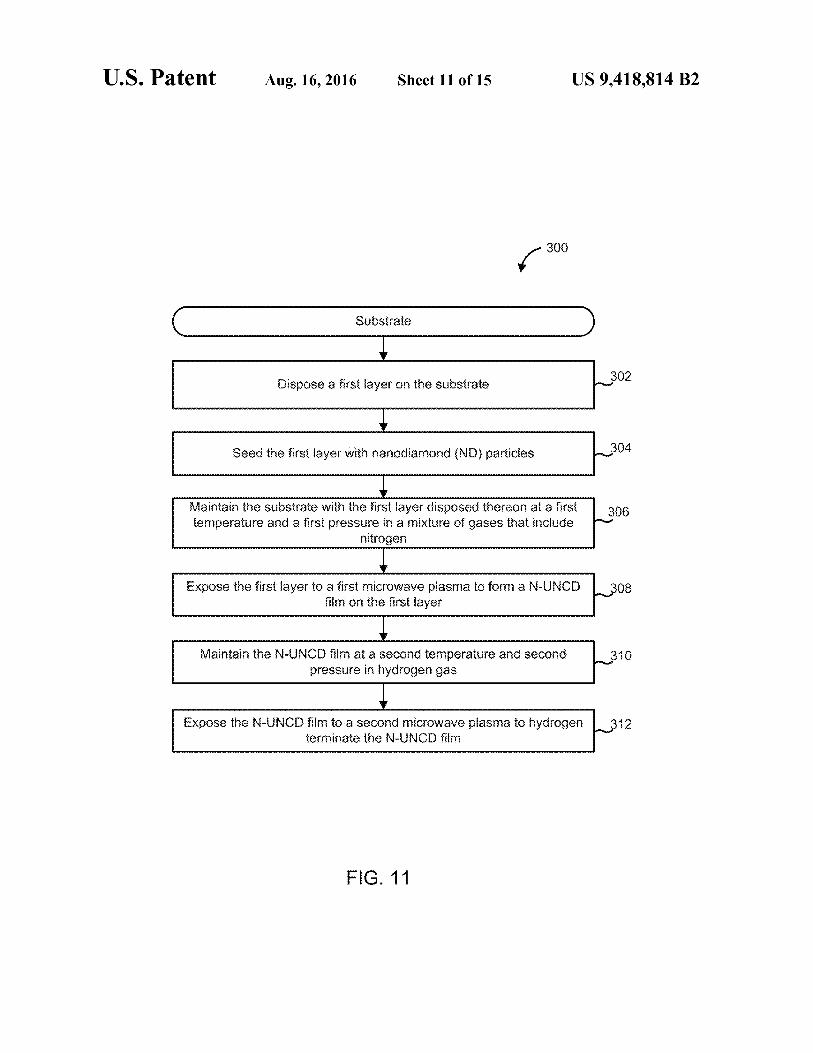
In some embodiments, a N-UNCD film can be terminatedwith hydrogen and used as a photocathode which is highlystable and can be operated under moderate vacuum, forexample at pressures of up to about 10-5
Torr. FIG. 11 is
schematic flow diagram of an exemplary method 300 forforming a photocathode that includes a hydrogen terminatedN-UNCD film (N-UNCD:H). The method 300 includes dis-posing a first layer on a substrate, at 302. The substrate caninclude metals such as, for example, stainless steel, molyb-denum, tungsten, niobium, gold, platinum, alloys, any othersuitable material or a combination thereof. In one embodi-ment, the substrate can include stainless steel. Use of thestainless steel substrate can yield a stable photocathode whichcan be mass produced, and is relatively cheap. The substratecan have any suitable shape or size. For example, the substratecan include a cylinder, a disc, a block, etc., and can have anysuitable cross-section, for example circular, square, rectan-
12gular, oval, polygonal, an asymmetric shape or any othershape. In particular embodiments, the substrate is planar. Insuch embodiment, the photocathode is planar.In some embodiment, the first layer includes a transition
5 metal such as, for example, molybdenum (Mo), titanium (Ti),tungsten (W), tantalum (Ta), niobium (Nb), rhenium (Rh),ruthenium (Ru), any other suitable transition metal or a com-bination thereof. In one embodiment, the first layer caninclude Mo, for example, a polycrystalline Mo substrate. The
io first layer can be disposed on the substrate using any suitablemethod such as sputtering, e-beam deposition, electroplating,any other suitable method or a combination thereof. Further-more, the first layer can have any suitable thickness, forexample about 50 nm to about 10 microns.
15 The first layer is seeded with nanodiamond (ND) particles,at 304. The ND particles can be in the form of a slurry andhave a size in the range of about 1 nm to about 20 nm (e.g.,about 1 mu, 2 mu, 4 mu, 6 mu, 8 mu, 10 mu, 12 mu, 14 mu, 16mu, 18 nm or about 20 mn inclusive of all ranges or values
20 therebetween) although larger sized ND particles can also beused (e.g., up to about 100 mu). In one embodiment, seedingis performed by immersing the substrate with the first layerdisposed thereon in a slurry of the ND particles and sonication(e.g., in an ultrasonic bath) for a predetermined period of
25 time. The ND particles promote rapid nucleation and growthof an N-UNCD film on first layer over the substrate.The substrate with the seeded first layer disposed thereon is
maintained at a first temperature and a first pressure in amixture of gases that include nitrogen, at 306. In some
30 embodiments, the pre-seeded substrate with the first layerdisposed thereon can be disposed in an MPCVD chamber.The substrate is heated to the first temperature which can be inthe range of about 650 degrees Celsius to about 950 degreesCelsius (e.g., 650 degrees Celsius, 700 degrees Celsius, 75
35 degrees Celsius, 800 degrees Celsius, 850 degrees Celsius,900 degrees Celsius or about 950 degrees Celsius inclusive ofall ranges and values therebetween). Furthermore, the firstpressure can be in the range of about 40 Torr to about 70 Torr(e.g., about 40 Torr, 45 Torr, 50 Torr, 55 Torr, 60 Torr, 65 Torr
40 or about 70 Torr inclusive of all ranges and values therebe-tween).As describedbefore themixture of gases includes nitrogen.
In one embodiments, the mixture of gases includes methane,argon and nitrogen. In some embodiments, amount of nitro-
45 gen in the mixture can be in a range of about 5 vol % to about20 vol %.The first layer is exposed to a first microwave plasma to
form a N-UNCD film on the first layer, at 308. In someembodiments, the microwave plasma can be produced using
5o a microwave plasma source (e.g., having a frequency of about915 MHz). Any suitable power can be applied on the plasmasource to produce the first microwave plasma, for example apower in the range of about 2 kW to about 3 kW (e.g., 2 kW,2.2 kW, 2.4 kW, 2.6 kW, 2.8 kW or about 3 kW inclusive of all
55 ranges and values therebetween).The N-UNCD film has a percentage of nitrogen in the
N-UNCD film in the range of about 0.05 atom % to about 0.5atom % (e.g., 0.06 atom %, 0.07 atom %, 0.08 atom %, 0.09atom %, 0.1 atom %, 0.12 atom %, 0.14 atom %, 0.16 atom %,
60 0.18 atom %, 0.2 atom %, 0.25 atom %, 0.3 atom %, 0.35atom %, 0.4 atom %, 0.45 atom % or about 0.5 atom %inclusive of all ranges and values therebetween). In someembodiments, a carrier concentration in the N-UNCD filmcan be about 1020 per cm3.
65 The N-UNCD film disposed on the substrate is maintainedat a second temperature and a second pressure in hydrogengas, at 310. The second temperature can be in the range of
US 9,418,814 B2
13about 600 degrees Celsius to about 900 degrees Celsius (e.g.,about 600 degrees Celsius, 650 degrees Celsius, 700 degreesCelsius, 750 degrees Celsius, 800 degrees Celsius, 850degrees Celsius, or about 900 degrees Celsius inclusive of allranges and values therebetween). The second pressure can bein the range of about 10-20 Torr (e.g., about 10 Torr, 12 Torr,14 Torr, 16 Torr, 18 Torr, or about 20 Torr inclusive of allranges and values therebetween). The hydrogen gas can beprovided at a flow rate of about 100-300 sccm (e.g., about 100sccm, 150 sccm, 200 sccm, 250 sccm, or about 300 sccminclusive of all ranges and values therebetween). In otherembodiments, the mixture of gases can include a source ofdeuterium such that the N-UNCD film is terminated withdeuterium instead of hydrogen.The N-UNCD film is then exposed to a second microwave
plasma to hydrogen terminate the N-UNCD film, at 312. Thesecond microwave plasma can be produced (e.g., using thesame 915 MHz plasma source as described before) using amicrowave power in the range of about 1 kW to about 5 kW(e.g., about 1 kW, 2 kW 3 kW, 4 kW, or about 5 kW inclusiveof all ranges and values therebetween). In this manner, aphotocathode that includes a N-UNCD:H film disposed overthe substrate (e.g., a stainless steel substrate) is formed. Insome embodiments, a carrier concentration in theN-UNCD:H film can be about 1020 per cm3. In some embodi-ments in which the mixture of gases includes deuteriuminstead of hydrogen, exposing the N-UNCD film to themicrowave plasma terminates the N-UNCD with deuterium.
In one embodiment, the N-UNCD:H film and thereby, thephotocathode formed using the method 300 has a quantumefficiency in the range of at least 5x10-$ electrons/photon(e.g., about 5x10-$ electrons/photon to about 5x10⁻⁹ elec-trons/photon or even higher) between a visible wavelength ofabout 405 nm to about 436 mu. In other embodiments, theN-UNCD:H film and thereby, the photocathode formed usingthe method 300 has a quantum efficiency of at least 10-3electrons/photon at wavelengths in range of about 240 nm toabout 270 mu. Thus, the photocathode formed using themethod 300 is responsive to ultraviolet (UV) as well as visiblewavelengths.
In still other embodiments the N-UNCD:H film andthereby, the photocathode formed using the method 300 has awork function in the range of about 2.9 eV to about 3.2 eVinclusive of all ranges and values therebetween.
In some embodiments, the method 300 can also includeoperating the photocathode until a performance of the pho-tocathode is depleted. For example, the hydrogen terminationof the N-UNCD:H films can degrade over a period of usage.In such embodiments, the photocathode can be exposed to ahydrogen plasma to restore the performance of thephotocath-ode.
FIG. 12 is a schematic illustration of a photocathode 400,according to an embodiment. The photocathode 400 can beformed using the method 300 or any other method describedherein. The photocathode 400 includes a planar substrate 410,a first layer 420, and a N-UNCD:H film 430.The planar substrate 410 can be formed from metals such
as, for example, stainless steel, molybdenum, tungsten, gold,platinum, niobium, alloys, any other suitable material or acombination thereof. In one embodiment, the planar substrate410 can include stainless steel. The planar substrate 410 canhave any suitable shape or size. For example, the planarsubstrate 410 can include a cylinder, a disc, a block, etc., andcan have any suitable cross-section, for example circular,square, rectangular, oval, polygonal, an asymmetric shape orany other shape.
14The first layer 420 is disposed over the planar substrate
210. In some embodiments, the first layer 220 includes atransition metal such as, for example, molybdenum (Mo),titanium (Ti), tungsten (W), tantalum (Ta), niobium (Nb),
5 rhenium (Rh), ruthenium (Ru), any other suitable transitionmetal or a combination thereof. In one embodiment, the firstlayer 420 can include Mo, for example, a polycrystalline Mosubstrate. The first layer 420 can be disposed on the planarsubstrate 410 using any suitable method such as sputtering,
io e-beam deposition, electroplating, any other suitable methodor a combination thereof. Furthermore, the first layer 420 canhave any suitable thickness, for example about 50 mn to about10 microns.The N-UNCD:H film 430 is disposed over the first layer
15 420. The first layer 420 can serve as a nucleation layer fordisposing an N-UNCD film 430 thereon, which is then ter-minated with hydrogen to form the N-UNCD:H film asdescribed with respect to method 300. The N-UNCD:H film230 has a percentage of nitrogen in the range of about 0.05
20 atom % to about 0.5 atom % (e.g., 0.06 atom %, 0.07 atom %,0.08 atom %, 0.09 atom %, 0.1 atom %, 0.12 atom %, 0.14atom %, 0.16 atom %, 0.18 atom %, 0.2 atom %, 0.25 atom %,0.3 atom %, 0.35 atom %, 0.4 atom %, 0.45 atom % or about0.5 atom % inclusive of all ranges and values therebetween).
25 In other embodiments, the N-UNCD films can be terminatedwith deuterium.The N-UNCD:H film 430 can have any suitable thickness,
for example in the range of about 30 nm to about 300 nm (e.g.,30 nm, 40 mu, 50 nm, 60 nm, 70 nm, 80 nm, 90 nm, 100 nm,
30 110 mu, 120 nm, 130 mu, 140 nm, 150 nm, 160 nm, 170 nm,180 nm, 190 mu, 200 nm, 250 nm or about 300 nm inclusiveof all ranges and values therebetween). In some embodi-ments, a carrier concentration in the N-UNCD:H film 430 isabout 1020 per cm3.
35 In one embodiment, the N-UNCD:H film 430 has a quan-tum efficiency in the range of at least 5 x 10-$ electrons/photon(e.g., about 5x10-$ to about 5x10⁻⁹ electrons/photon or evenhigher), between a visible wavelength of about 405 nm toabout 436 nm. In other embodiments, the N-UNCD:H film
4o 430 has a quantum efficiency of at least 10-3 electrons/photonat wavelengths in range of about 240 mn to about 270 mu. Instill other embodiments the N-UNCD:H film 430 has a workfunction in the range of about 2.9 eV to about 3.2 eV inclusiveof all ranges and values therebetween.
45 The photocathode 400 is robust, has high stability and hashigh efficiency. The photocathode 400 is operable at moder-ate vacuum conditions up to apressure of about 10-5 Torr. Thephotocathode 400 can be used in numerous applications suchas, for example, as an electron injector in synchrotrons, free
50 electron lasers, linacs, and ultrafast electron systems forimaging and diffraction. Furthermore, the photocathode 400is operational in the near UV range (i.e., 250 mn to 270 mu)as well as in the visible range (i.e., 405 nm to 436 nm).In some embodiments, a quantum efficiency of the
55 N-UNCD:H film 430 included in the photocathode 400 canbe rejuvenated in situ in an electron injector if it is degraded.For example, an electron injector can be filled with hydrogengas instead of evacuating to vacuum. An RF source which isconventionally used for electron acceleration, can be used to
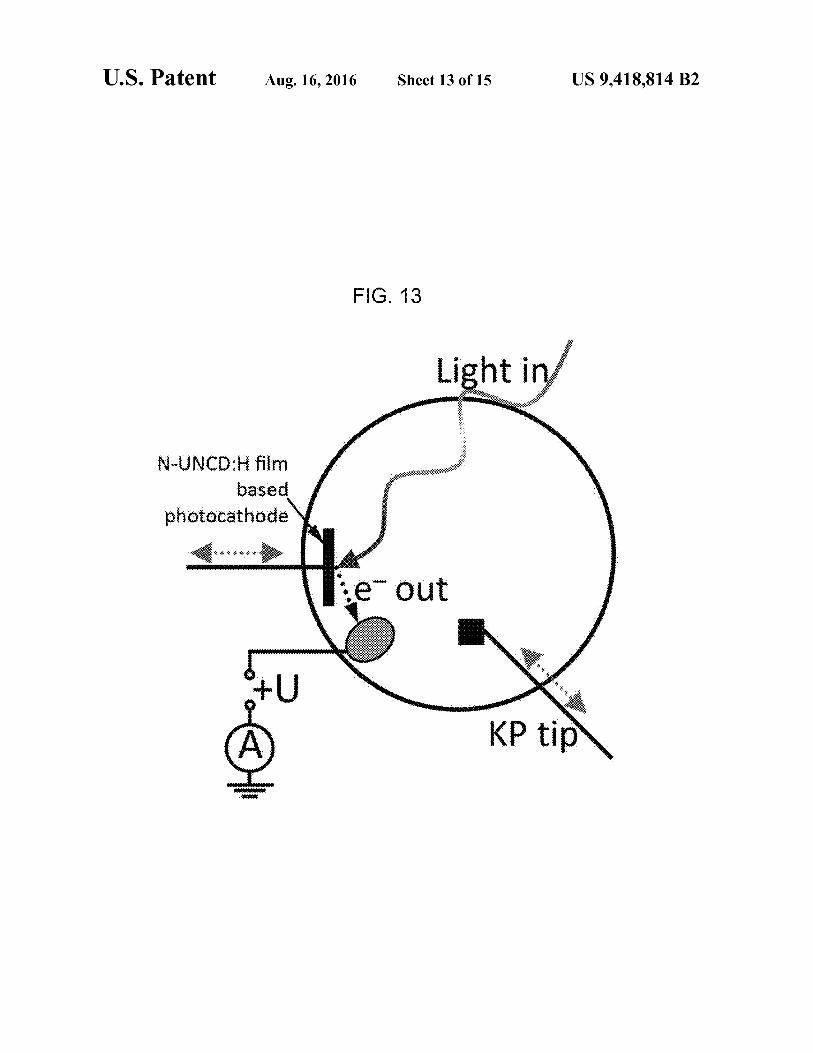
60 ignite the hydrogen plasma (e.g., at a lower power of anaccelerator power source). This restores the performance ofthe N-UNCD:H film. The hydrogen can then be evacuatedand vacuum restored.FIG. 13 is a schematic illustration of a Kelvin probe (KP)
65 instrument (KP6500 from McAllister Technical Service) forperforming work function (WF) and quantum efficiency (QE)measurements on N-UNCD: H photocathodes. The KP instru-

US 9,418,814 B2
15ment has custom modifications for measuring WF and QE ofthe N-UNCD:H photocathode in the same experimental run.N-UNCD:H photocathodes were formed using a variation
of the method 300. An N-UNCD film was formed on a steelsubstrate which includes a polycrystalline molybdenum layerdisposed thereon using a substantially similar method used toform the field emitter of FIG. 3 and therefore not described infurther detail herein. The N-UNCD film had a thickness ofabout 150 mu. A carrier concentration of the N-UNCD filmwas about 1020 per cm3. The N-UNCD film disposed on thepolycrystalline molybdenum was H terminated in the sameMPCVD chamber which was used to grow the N-UNCD filmon the stainless steel/molybdenum substrate. The substratewas heated and maintained at a temperature of about 750degrees Celsius. Hydrogen gas at a flow rate of about 200sccm was introduced into the chamber and the pressure wasmaintained at a pressure of about 15 Torr. The N-UNCD filmwas exposed to a microwave plasma at a frequency of about915 MHz and a power of about 2 kW for about 15 minutes toyield the N-UNCD:H film on the polycrystalline molybde-num layer and form the photocathode. The photocathode wasallowed to cool down to room temperature in the synthesischamber.
Before or after termination, all samples were taken fromthe MPCVD chamber and transported to the KP instrumentchamber under ambient conditions. Total exposure time inambient air was about 2 hours. The KP chamber was evacu-ated during all measurements to a base pressure of about10-5-10-6 Torr. A voltage of +300V was applied to a smallaluminum anode plate, and a current of photoelectrons to theground was collected by the same source/ammeter (Keithley6487) with a threshold sensitivity of about ±10 femtoAmps.The anode plate was introduced into the KP chamber at an
angle such that it did not interfere with the light beam and thetip measuring the WE The sample holder actuator and the KPtip are both retractable, such that ideal positions can be foundfor QE and WF measurements independently. The WFs forN-UNCD films were determined by the KP with respect to itscalibrated tip (WF=4.6 eV) before and after N-UNCD filmunderwent hydrogen plasma treatment. A sample holdermade of standard polycrystalline copper was used as a refer-ence. All deduced WF values are plotted in FIG. 14. WFdependence on time is a standard representation for KP toestimate the signal's noise and drift with respect to time andget a confident measurement of a WE As seen in FIG. 14, theWFs of the N-UNCD:H films were lower than the WFs of theplain N-UNCD film and the polycrystalline copper reference.QE measurements were performed using an arc broadband
Hg lamp (Spectra-Physics/Newport Oriel Instruments series66900) as a light source. A light spot size from the source wasadjusted by an aperture and focused by a lens. The spot size onthe N-UNCD film surface was about 1 mm2. A number offilters were used to define a spectral dependence of N-UNCDQE before and after hydrogen termination, namely 254, 313,365, 405, and 436 mu. The output power of the lamp P(X) ateach filtered wavelength was assessed by a calibrated powermeter (Ophir Nova II), equipped with a calibrated photodiode(Ophir PD300-UV). The photoelectron current IPh..(X) wasrecorded at each wavelength. QEs were calculated as:
yeae~ro (~)
where number of electrons NeteCtb s(~) per second is iphoto(X)/e,
16and number of photons per second NeZe~ o s(~) is P(X) [eV/s]/(hv) [eV] with e being the elementary electron charge andby being a single photon energy. Moreover,
5 P(T) [eV/s]=P(T) [W]/e and by [eV]=1240/T [nm].
iph..(X) [Amps] and P(X) [W]/ are experimentally measuredquantities. All numbers are compiled and plotted in FIG. 15.As seen in FIG. 15, the N-UNCD:H films has a sensitivity
shifted toward near UV/visible wavelengths. There are two10 notable features in FIG. 15. The first feature is QE in the band
250-270 mu, whichis of common interest to thephotocathodecommunity. QE of the N-UNCD film without H terminationwas about 5x10⁻⁶. Given the measured WF of 3.6 eV, this isa quite moderate effect compared to the single crystal copper
15 (100) which has a QE of about 5x1 0-s and a WF=4.2 eV.However, the QE was enhanced by a factor of 140 uponH-termination, placing N-UNCD:H at the low boundary of aQE range of alkali-based photocathodes.
Furthermore, the N-UNCD:H films were responsive in20 visible blue light. KP results show that in all cases, the pho-
toemission was in the sub-WF regime. This can be explainedby enhanced emission from grain boundaries with a loweredWF, caused by the local environment, accounted also forstrong field emission from flat polycrystalline N-UNCD:H
25 surfaces. Photoemission from N-UNCD:H in visible blue at405 mu is possibly a regular threshold process and correlatesto a photon energy of 3.06 eV versus WF 3.07±0.01 eV and3.15±0.01 eV as determined by KP measurements. In any ofthe two regimes, incorporation of nitrogen leads to sustain-
3o able currents of about 10 pA from N-UNCD: H surfaces usingblue light.
Thus, the N-UNCD:H photocathodes can provide stableand robust cathodes which are operable in both the UV andvisible regimes. Furthermore, the N-UNCD: H photocathodes
35 can be operable at much higher pressures than conventionalphotocathodes, for example up to pressures of about 10-5
Torr, while providing the QE and WF comparable with con-ventional alkali photocathodes performing exclusively onlyin ultrahigh vacuum.
40 As used herein, the singular forms "a", "an" and "the"include plural referents unless the context clearly dictatesotherwise. Thus, for example, the term "a member" isintended to mean a single member or a combination of mem-bers, "a material" is intended to mean one or more materials,
45 or a combination thereof.As used herein, the terms "about" and "approximately"
generally mean plus or minus 10% of the stated value. Forexample, about 0.5 would include 0.45 and 0.55, about 10would include 9 to 11, about 1000 would include 900 to 1100.
50 It should be noted that the term "exemplary" as used hereinto describe various embodiments is intended to indicate thatsuch embodiments are possible examples, representations,and/or illustrations of possible embodiments (and such termis not intended to connote that such embodiments are neces-
55 sarily extraordinary or superlative examples).The terms "coupled," "connected," and the like as used
herein mean the joining of two members directly or indirectlyto one another. Such joining may be stationary (e.g., perma-nent) or moveable (e.g., removable or releasable). Such join-
60 ing may be achieved with the two members or the two mem-bers and any additional intermediate members beingintegrally formed as a single unitary body with one another orwith the two members or the two members and any additionalintermediate members being attached to one another.
65 It is important to note that the construction and arrange-ment of the various exemplary embodiments are illustrativeonly. Although only a few embodiments have been described

US 9,418,814 B2
17in detail in this disclosure, those skilled in the art who reviewthis disclosure will readily appreciate that many modifica-tions are possible (e.g., variations in sizes, dimensions, struc-tures, shapes and proportions of the various elements, valuesof parameters, mounting arrangements, use of materials, col-ors, orientations, etc.) without materially departing from thenovel teachings and advantages of the subject matterdescribed herein. Other substitutions, modifications, changesand omissions may also be made in the design, operatingconditions and arrangement of the various exemplaryembodiments without departing from the scope of the presentinvention.
What is claimed is:1. A method of forming a field emitter, comprising:disposing a first layer on a substrate;seeding the first layer with nanodiamond particles;maintaining the substrate with the seeded first layer dis-posed thereon at a first temperature and a first pres sure ina mixture of gases, the mixture including nitrogen; and
exposing the first layer to a microwave plasma to form anitrogen doped ultrananocrystalline diamond film on thefirst layer, the nitrogen doped ultrananocrystalline dia-mond film having a percentage of nitrogen in the rangeof about 0.05 atom % to about 0.5 atom %,
wherein, the field emitter has about 1012 to about 1014emitting sites per cm2.
2. The method of claim 1, wherein the first layer includes atransition metal.
3. The method of claim 2, wherein the first layer includes atleast one of molybdenum and niobium.
4. The method of claim 1, wherein the first temperature isin the range of about 650 degrees Celsius to about 950 degreesCelsius.
5. The method of claim 1, wherein the first pressure is in therange of about 40 Torr to about 70 Torr.
6. The method of claim 1, wherein the substrate is at leastone of planar, microstructured and nanostructured.
7. The method of claim 5, wherein the substrate includesstainless steel.
8. The method of claim 5, wherein the substrate is planarand wherein the nitrogen doped ultrananocrystalline dia-mond film has a current density in the range of about 0.1mAmp/cm2 to about at least 25 mAmp/cm2 between an elec-tric field gradient of about 45 MV/m to about 65 MV/m,respectively.
9. The method of claim 1, wherein the nitrogen dopedultrananocrystalline diamond film has a beam emittance inthe range of about 0.5 mmxmrad/mm-rms to about 3mmxmrad/mm-rms at 65 MV/m.
10. The method of claim 1, wherein the nitrogen dopedultrananocrystalline diamond film has a full width half maxi-mum longitudinal energy spread of about 0.5% to about 1%.
11. A method of forming a photocathode, comprising:disposing a first layer on a substrate;seeding the first layer with nanodiamond particles;maintaining the substrate with the seeded first layer dis-posed thereon at a first temperature and a first pres sure ina mixture of gases, the mixture including nitrogen;
exposing the first layer to a microwave plasma to form anitrogen doped ultrananocrystalline diamond film on thefirst layer, the nitrogen doped ultrananocrystalline dia-mond film having a percentage of nitrogen in the rangeof about 0.05 atom % to about 0.5 atom %;
maintaining the nitrogen doped ultrananocrystalline dia-mond film at a second temperature and second pressurein hydrogen gas; and
18exposing the nitrogen doped ultrananocrystalline diamond
film to a microwave plasma to hydrogen terminate thenitrogen doped ultrananocrystalline diamond film.
12. The method of claim 11, wherein the first layer includes5 a transition metal.
13. The method of claim 11, wherein the first temperatureis in the range of about 650 degrees Celsius to about 950degrees Celsius.14. The method of claim 11, wherein the first pressure is in
10 the range of about 40 Torr to about 70 Torr.15. The method of claim 11, wherein the substrate is stain-
less steel.16. The method of claim 11, wherein the hydrogen termi-
15 nated nitrogen doped ultrananocrystalline diamond film has aquantum efficiency of at least 5x10-$ electrons/photonsbetween a visible wavelength range of about 405 nm to about436 mu, respectively.
17. The method of claim 11, wherein the hydrogen termi-
20 nated nitrogen doped ultrananocrystalline diamond film has aquantum efficiency of at least 10-3 electrons/photons at wave-lengths in the range of about 240 mn to about 270 mu.
18. The method of claim 11, further comprising:operating the photocathode until a performance of the pho-
25 tocathode is depleted; andexposing the photocathode to an hydrogen plasma to
restore the performance of the photocathode.19. A field emitter, comprising:a planar substrate;
30 a first layer disposed on the planar substrate; anda nitrogen doped ultrananocrystalline diamond film dis-
posed on the first layer, the nitrogen doped ultrananoc-rystalline diamond film having a percentage of nitrogen
35 in the range of about 0.05 atom % to about 0.5 atom %,wherein, the field emitter has about 1012 to about 1014
emitting sites per cm2.20. The field emitter of claim 19, wherein the nitrogen
doped ultrananocrystalline diamond film has a current den-40 sity in the range of about 0.3 mAmp/cm2 to about 25 mAmp/
cm2 at an electric field gradient of about 45 MV/m to about 65MV/m, respectively.21. The field emitter of claim 19, wherein the nitrogen
doped ultrananocrystalline diamond film has a beam emit-45 tance in the range of about 0.5 mmxmrad/mm-rms to about 3
mmxmrad/mm-rms.22. The field emitter of claim 19, wherein the nitrogen
doped ultrananocrystalline diamond film has a full width halfmaximum longitudinal energy spread of about 0.5% to about
50 1%.23. The field emitter of claim 19, wherein the field emitter
is operable via a radio frequency energy source.24. The field emitter of claim 19, wherein the planar sub-
strate is formed from stainless steel.55 25. A photocathode, comprising:
a substrate;a first layer disposed on the substrate; anda hydrogen terminated nitrogen doped ultrananocrystalline
diamond film disposed on the first layer, the hydrogen60 terminated nitrogen doped ultrananocrystalline dia-
mond film having a percentage of nitrogen in the rangeof about 0.05 atom % to about 0.5 atom %,
wherein, the photocathode has about 1012 to about 1014
emitting sites per cm2.65 26. The photocathode of claim 25, wherein the hydrogen
terminated nitrogen doped ultrananocrystalline diamond filmhas a quantum efficiency in the range of about 5x10-$ elec-

US 9,418,814 B2
19 20trons/photons to about 5x10⁻⁹ electrons/photons between avisible wavelength range of about 405 nm to about 436 mu,respectively.
27. The photocathode of claim 26, wherein the hydrogenterminated nitrogen doped ultrananocrystalline diamond film 5
has a quantum efficiency of about 10-3 electrons/photons atwavelengths in the range of about 240 nm to about 270 mu.
28. The photocathode of claim 26, wherein the photocath-ode is operable at a pressure of up to about 10-5 Torr.
29. The photocathode of claim 26, wherein the nitrogen iodoped ultrananocrystalline diamond film is terminated withdeuterium.