Embed Size (px)
Citation preview

USB3500Hi-Speed USB Host, Device or OTG PHY
With UTMI+ Interface
Highlights
• USB-IF “Hi-Speed” certified to the Universal Serial Bus Specification Rev 2.0
• Interface compliant with the UTMI+ Specification, Revision 1.0
• Includes full support for the optional On-The-Go (OTG) protocol detailed in the On-The-Go Sup-plement Revision 1.0a specification
• Functional as a host, device or OTG PHY
• Supports HS, FS, and LS data rates
• Supports FS pre-amble for FS hubs with a LS device attached (UTMI+ Level 3)
• Supports HS SOF and LS keep alive pulse.
• Supports Host Negotiation Protocol (HNP) and Session Request protocol (SRP)
• Internal comparators support OTG monitoring of VBUS levels
• Low Latency Hi-Speed Receiver (43 Hi-Speed clocks Max)
• Internal 1.8 volt regulators allow operation from a single 3.3 volt supply
• Internal short circuit protection of ID, DP and DM lines to VBUS or ground
• Integrated 24MHz Crystal Oscillator supports either crystal operation or 24MHz external clock input
• Internal PLL for 480MHz Hi-Speed USB operation
• Supports USB 2.0 and legacy USB 1.1 devices
• 55mA Unconfigured Current (typical) - ideal for bus powered applications
• 83uA suspend current (typical) - ideal for battery powered applications
• Full Commercial operating temperature range from 0C to +70C
• 56-Pin, QFN RoHS compliant package (8 x 8 x 0.90 mm height)
Functional Overview
The USB3500 is a highly integrated USB transceiversystem. It contains a complete USB 2.0 PHY with theUTMI+ industry standard interface to support fast timeto market for a USB controller. The USB3500 is com-posed of the functional blocks shown in the figurebelow.
USB3500 Block Diagram
UTMI+Digital
OTGModule
24 MHzXTAL
InternalRegulators
& POR
5VPowerSupply
BiasGen.
XCVRSEL[1:0]
VDD3.3 XTAL &PLL
XI
VBUS
ID
VDD3.3
DPDM
USB3500
VD
D1
.8
VD
DA
1.8 m
XO
RBIAS
Mini-ABUSB
Connector
HS XCVR
FS/LSXCVR
Resistors
Rp
u_
dp
Rp
d_
dm
Rp
d_
dp
Rp
u_
dm
TERMSELTXREADY
SUSPENDNTXVALIDRESET
CHRGVBUSRXACTIVE
OPMODE[1:0]ID_DIG
IDPULLUPCLKOUT
LINESTATE[1:0]HOSTDISC
DISCHRGVBUSSESSENDDATA[7:0]RXVALIDSESSVLD
DPPDDMPD
RXERRORVBUSVLD
TXLogic
RXLogic
2005 - 2016 Microchip Technology Inc. DS00002103A-page 1

USB3500
TO OUR VALUED CUSTOMERS
It is our intention to provide our valued customers with the best documentation possible to ensure successful use of your Microchipproducts. To this end, we will continue to improve our publications to better suit your needs. Our publications will be refined andenhanced as new volumes and updates are introduced.
If you have any questions or comments regarding this publication, please contact the Marketing Communications Department viaE-mail at [email protected]. We welcome your feedback.
Most Current Data SheetTo obtain the most up-to-date version of this data sheet, please register at our Worldwide Web site at:
http://www.microchip.com
You can determine the version of a data sheet by examining its literature number found on the bottom outside corner of any page. The last character of the literature number is the version number, (e.g., DS30000000A is version A of document DS30000000).
ErrataAn errata sheet, describing minor operational differences from the data sheet and recommended workarounds, may exist for cur-rent devices. As device/documentation issues become known to us, we will publish an errata sheet. The errata will specify therevision of silicon and revision of document to which it applies.
To determine if an errata sheet exists for a particular device, please check with one of the following:• Microchip’s Worldwide Web site; http://www.microchip.com• Your local Microchip sales office (see last page)
When contacting a sales office, please specify which device, revision of silicon and data sheet (include -literature number) you areusing.
Customer Notification SystemRegister on our web site at www.microchip.com to receive the most current information on all of our products.
DS00002103A-page 2 2005 - 2016 Microchip Technology Inc.
2005 - 2016 Microchip Technology Inc. DS00002103A-page 3
USB3500
Table of Contents
1.0 General Description ........................................................................................................................................................................ 42.0 Pin Configuration and Pin Definitions ............................................................................................................................................. 63.0 Limiting Values .............................................................................................................................................................................. 114.0 Electrical Characteristics ............................................................................................................................................................... 125.0 Detailed Functional Description .................................................................................................................................................... 166.0 Application Notes .......................................................................................................................................................................... 257.0 Package Outline ............................................................................................................................................................................ 39Appendix A: Revision History .............................................................................................................................................................. 41The Microchip Web Site ...................................................................................................................................................................... 42Customer Change Notification Service ............................................................................................................................................... 42Customer Support ............................................................................................................................................................................... 42Product Identification System ............................................................................................................................................................. 43

USB3500
1.0 GENERAL DESCRIPTION
The USB3500 is a stand-alone Hi-Speed USB Physical Layer Transceiver (PHY). The USB3500 uses a UTMI+ interfaceto connect to an SOC or FPGA or custom ASIC. The USB3500 provides a flexible alternative to integrating the analogPHY block for new designs.
The USB3500 provides a fully compliant USB 2.0 interface, and supports High-Speed (HS), Full-Speed (FS), and Low-Speed (LS) USB. The USB3500 supports all levels of the UTMI+ specification as shown in Figure 1-2.
The USB3500 can also, as an option, fully support the On-the-Go (OTG) protocol defined in the On-The-Go Supplementto the USB 2.0 Specification. On-the-Go allows the Link to dynamically configure the USB3500 as host or peripheralconfigured dynamically by software. For example, a cell phone may connect to a computer as a peripheral to exchangeaddress information or connect to a printer as a host to print pictures. Finally the OTG enabled device can connect toanother OTG enabled device to exchange information. All this is supported using a single low profile Mini-AB USB con-nector.
Designs not needing OTG can ignore the OTG feature set.
FIGURE 1-1: BASIC UTMI+ USB DEVICE BLOCK DIAGRAM
SOC/FPGA/ASICIncluding Device Controller
USB3500
USB 2.0Analogw/ OTG
USBConnector(Standard
or Mini)
DM
VBUS
DP
IDHi-SpeedUSB App.
UTMI+Interface
UTMI+DigitalLogic
UTMI+Link
DS00002103A-page 4 2005 - 2016 Microchip Technology Inc.

USB3500
The USB3500 uses Microchip’s advanced proprietary technology to minimize power dissipation, resulting in maximizedbattery life in portable applications.
1.1 Applications
The USB3500 is targeted for any application where a hi-speed USB connection is desired.
The USB3500 is well suited for:
• Cell Phones
• MP3 Players
• Scanners
• Printers
• External Hard Drives
• Still and Video Cameras
• Portable Media Players
• Entertainment Devices
1.2 Reference Documents
• Universal Serial Bus Specification, Revision 2.0, April 27, 2000
• USB 2.0 Transceiver Macrocell Interface (UTMI) Specification, Version 1.02, May 27, 2000
• On-The-Go Supplement to the USB 2.0 Specification, Revision 1.0a, June 24, 2003
• UTMI+ Specification, Revision 1.0, February 2, 2004
FIGURE 1-2: UTMI+ LEVEL 3 SUPPORT
UTMI+ Level 0USB2.0 Peripherals Only
AD
DE
D F
EA
TU
RE
S
USB3500UTMI+ Level 3
USB2.0 Peripheral, host controllers, On-the-Go devices
(HS, FS, LS, preamble packet)
UTMI+ Level 2USB2.0 Peripheral, host controllers, On-
the-Go devices(HS, FS, and LS but no preamble packet)
UTMI+ Level 1USB2.0 Peripheral, host controllers, and
On-the-Go devices(HS and FS Only)
USB3280USB3250
2005 - 2016 Microchip Technology Inc. DS00002103A-page 5

USB3500
2.0 PIN CONFIGURATION AND PIN DEFINITIONS
The USB3500 is offered in a 56-pin QFN package. The pin definitions and locations are documented below.
2.1 USB3500 Pin Locations
The flag of the QFN package must be connected to ground with a via array.
2.2 Pin Definitions
FIGURE 2-1: USB3500 PINOUT - TOP VIEW
TABLE 2-1: USB3500 PIN DEFINITIONS
Pin NameDirection,
Type ActiveLevel
Description
1 VSS Ground N/A PHY ground.
2 XCVRSEL[0] Input N/A Transceiver Select. These signals select between the FS and HS transceivers:Transceiver select.00: HS01: FS10: LS11: LS data, FS rise/fall times
3 TERMSEL Input N/A Termination Select. This signal selects between the FS and HS terminations:0: HS termination enabled1: FS termination enabled
IDP
UL
LU
P
XC
VR
SE
L1
LIN
ES
TA
TE
[0]
LIN
ES
TA
TE
[1]
OP
MO
DE
[1]
OP
MO
DE
[0]
CH
RG
VB
US
RX
AC
TIV
E
ID_
DIG
VS
S
CL
KO
UT
VS
S
VD
D1
.8
VD
D3
.3
SESSVLD
DATA[1]
DATA[0]
DATA[2]
DATA[3]
DATA[4]
DATA[5]
DATA[6]
DATA[7]
RXVALID
VSS
SESSEND
DISCHRGVBUS
HOSTDISC
RB
IAS
VD
D3
.3
VD
D3
.3
VD
DA
1.8
XI
XO
VS
S
VD
D1
.8
VB
US
VL
D
VD
D3
.3
VS
S
RX
ER
RO
R
DM
PD
DP
PD
VSS
DM
DP
VDD3.3
VSS
VDD3.3
RESET
TXVALID
SUSPENDN
ID
VBUS
TXREADY
TERMSEL
XCVRSEL0
10
11
12
13
14
15
16
17
18
19
20
21
22
23
24
25
26
27
28
42
41
29
30
31
32
34
35
36
37
38
39
40
33
48
47
46
45
44
43
56
55
54
53
52
51
50
49
1
2
3
4
5
6
7
8
9
USB3500Hi-Speed USBUTMI+ PHY56 Pin QFN
GND FLAG
DS00002103A-page 6 2005 - 2016 Microchip Technology Inc.
USB3500
4 TXREADY Output High Transmit Data Ready. If TXVALID is asserted, the Link must always have data available for clocking into the TX Holding Register on the rising edge of CLKOUT. TXREADY is an acknowledgment to the Link that the transceiver has clocked the data from the bus and is ready for the next transfer on the bus. If TXVALID is negated, TXREADY can be ignored by the Link.
5 VBUS I/O,Analog
N/A VBUS pin of the USB cable.
6 ID Input,Analog
N/A ID pin of the USB cable.
7 SUSPENDN Input Low Suspend. Places the transceiver in a mode that draws minimal power from supplies. In host mode, RPU is removed during suspend. In device mode, RPD is controlled by TERMSEL. In suspend mode the clocks are off.0: PHY in suspend mode1: PHY in normal operation
8 TXVALID Input High Transmit Valid. Indicates that the DATA bus is valid for transmit. The assertion of TXVALID initiates the transmission of SYNC on the USB bus. The negation of TXVALID initiates EOP on the USB.
Control inputs (OPMODE[1:0], TERMSEL,XCVERSEL) must not be changed on the de-assertion or assertion of TXVALID.
9 RESET Input High Reset. Reset all state machines. After coming out of reset, must wait 5 rising edges of clock before asserting TXValid for transmit. Assertion of Reset: May be asynchronous to CLKOUTDe-assertion of Reset: Must be synchronous to CLKOUT
10 VDD3.3 N/A N/A 3.3V PHY Supply. Provides power for USB 2.0 Transceiver, UTMI+ Digital, Digital I/O, and Regulators.
11 DP I/O,Analog
N/A D+ pin of the USB cable.
12 DM I/O,Analog
N/A D- pin of the USB cable.
13 VSS Ground N/A PHY ground.
14 VDD3.3 N/A N/A 3.3V PHY Supply.
15 XCVRSEL[1] Input N/A Transceiver Select. These signals select between the FS and HS transceivers:Transceiver select.00: HS01: FS10: LS11: LS data, FS rise/fall times
16 CHRGVBUS Input High Charge VBUS through a resistor to VDD3.3.0: do not charge VBUS1: charge VBUS
17 RXACTIVE Output High Receive Active. Indicates that the receive state machine has detected Start of Packet and is active.
18 OPMODE[1] Input N/A Operational Mode. These signals select between the various operational modes:[1] [0] Description0 0 0: Normal Operation0 1 1: Non-driving (all terminations removed)1 0 2: Disable bit stuffing and NRZI encoding1 1 3: Reserved
19 OPMODE[0] Input N/A
TABLE 2-1: USB3500 PIN DEFINITIONS (CONTINUED)
Pin NameDirection,
Type ActiveLevel
Description
2005 - 2016 Microchip Technology Inc. DS00002103A-page 7

USB3500
20 ID_DIG Output High ID Digital. Indicates the state of the ID pin. 0: connected plug is a mini-A1: connected plug is a mini-B
21 IDPULLUP Input High ID Pull-up. Enables sampling of the analog ID line. Disabling the ID line sampler will reduce PHY power consumption.0: Disable sampling of ID line.1: Enable sampling of ID line.
22 VSS Ground N/A PHY ground.
23 CLKOUT Output,CMOS
N/A 60MHz reference clock output. All UTMI+ signals are driven synchronous to this clock.
24 VSS Ground N/A PHY ground.
25 LINESTATE[1] Output N/A Line State. These signals reflect the current state of the USB data bus in FS mode. Bit [0] reflects the state of DP and bit [1] reflects the state of DM. When the device is suspended or resuming from a suspended state, the signals are combinatorial. Otherwise, the signals are synchronized to CLKOUT.[1] [0] Description0 0 0: SEO0 1 1: J State1 0 2: K State1 1 3: SE1
26 LINESTATE[0] Output N/A
27 VDD1.8 N/A N/A 1.8V regulator output for digital circuitry on chip. Place a 0.1uF capacitor near this pin and connect the capacitor from this pin to ground. Connect pin 27 to pin 49.
28 VDD3.3 N/A N/A 3.3V PHY Supply. Provides power for USB 2.0 Transceiver, UTMI+ Digital, Digital I/O, and Regulators.
29 HOSTDISC Output High Host Disconnect. In HS Host mode this indicates to that a downstream device has been disconnected. Automatically reset to 0b when Low Power Mode is entered.
30 DISCHRGVBUS Input High Discharge VBUS through a resistor to ground.0: do not discharge VBUS1: discharge VBUS
31 SESSEND Output High Session End. Indicates that the voltage on Vbus is below its B-Device Session End threshold. 0: VBUS > VSessEnd1: VBUS < VSessEnd
TABLE 2-1: USB3500 PIN DEFINITIONS (CONTINUED)
Pin NameDirection,
Type ActiveLevel
Description
DS00002103A-page 8 2005 - 2016 Microchip Technology Inc.

USB3500
32 DATA[7] I/O,CMOS,Pull-low
N/A 8-bit bi-directional data bus. Data[7] is the MSB and Data[0] is the LSB.
33 DATA[6] I/O,CMOS,Pull-low
N/A
34 DATA[5] I/O,CMOS,Pull-low
N/A
35 DATA[4] I/O,CMOS,Pull-low
N/A
36 DATA[3] I/O,CMOS,Pull-low
N/A
37 DATA[2] I/O,CMOS,Pull-low
N/A
38 DATA[1] I/O,CMOS,Pull-low
N/A
39 DATA[0] I/O,CMOS,Pull-low
N/A
40 VSS Ground N/A PHY ground.
41 RXVALID Output High Receive Data Valid. Indicates that the DATA bus has received valid data. The Receive Data Holding Register is full and ready to be unloaded. The Link is expected to register the DATA bus on the next rising edge of CLKOUT.
42 SESSVLD Output High Session Valid. Indicates that the voltage on Vbus is above the indicated threshold. 0: VBUS < VSessVld1: VBUS > VSessVld
43 DPPD Input N/A DP Pull-down Select. This signal enables the 15k Ohm pull-down resistor on the DP line.0: Pull-down resistor not connected to DP1: Pull-down resistor connected to DP
44 DMPD Input N/A DM Pull-down Select. This signal enables the 15k Ohm pull-down resistor on the DM line.0: Pull-down resistor not connected to DM1: Pull-down resistor connected to DM
45 RXERROR Output High Receive Error. This output is clocked with the same timing as the receive DATA lines and can occur at anytime during a transfer. 0: Indicates no error.1: Indicates a receive error has been detected.
46 VSS Ground N/A PHY ground.
47 VBUSVLD Output High VBUS Valid. Indicates that the voltage on Vbus is above the indicated threshold. 0: VBUS < VVbusVld1: VBUS > VVbusVld
48 VDD3.3 N/A N/A 3.3V PHY Supply. Provides power for USB 2.0 Transceiver, UTMI+ Digital, Digital I/O, and Regulators.
TABLE 2-1: USB3500 PIN DEFINITIONS (CONTINUED)
Pin NameDirection,
Type ActiveLevel
Description
2005 - 2016 Microchip Technology Inc. DS00002103A-page 9

USB3500
49 VDD1.8 N/A N/A 1.8V regulator output for digital circuitry on chip. Place a 4.7uF low ESR capacitor near this pin and connect the capacitor from this pin to ground. Connect pin 49 to pin 27. See Section 5.6, "Internal Regulators and POR," on page 22.
50 VSS Ground N/A PHY ground.
51 XO Output,Analog
N/A Crystal pin. If using an external clock on XI this pin should be floated.
52 XI Input,Analog
N/A Crystal pin. A 24MHz crystal is supported. The crystal is placed across XI and XO. An external 24MHz clock source may be driven into XI in place of a crystal.
53 VDDA1.8 N/A N/A 1.8V regulator output for analog circuitry on chip. Place a 0.1uF capacitor near this pin and connect the capacitor from this pin to ground. In parallel, place a 4.7uF low ESR capacitor near this pin and connect the capacitor from this pin to ground. See Section 5.6, "Internal Regulators and POR".
54 VDD3.3 N/A N/A 3.3V PHY Supply. Provides power for USB 2.0 Transceiver, UTMI+ Digital, Digital I/O, and Regulators.
55 VDD3.3 N/A N/A 3.3V PHY Supply. Should be connected directly to pin 54.
56 RBIAS Analog,CMOS
N/A External 1% bias resistor. Requires a 12KΩ resistor to ground.
GND FLAG Ground N/A Ground. The flag must be connected to the ground plane.
TABLE 2-1: USB3500 PIN DEFINITIONS (CONTINUED)
Pin NameDirection,
Type ActiveLevel
Description
DS00002103A-page 10 2005 - 2016 Microchip Technology Inc.

2005 - 2016 Microchip Technology Inc. DS00002103A-page 11
USB3500
3.0 LIMITING VALUES
TABLE 3-1: MAXIMUM RATINGS
Parameter Symbol Condition MIN TYP MAX Units
Maximum VBUS, ID, DP, and DM voltage to Ground
VMAX_5V -0.5 +5.5 V
Maximum VDD1.8 and VDDA1.8 voltage to Ground
VMAX_1.8V -0.5 2.5 V
Maximum 3.3V supply voltage to Ground
VMAX_3.3V -0.5 4.0 V
Maximum I/O voltage to Ground
VMAX_IN -0.5 4.0 V
Operating Temperature TMAX_OP 0 70 C
Storage Temperature TMAX_STG -55 150 C
Note: Stresses above those listed could cause damage to the device. This is a stress rating only and functionaloperation of the device at any other condition above those indicated in the operation sections of this spec-ification is not implied. When powering this device from laboratory or system power supplies, it is importantthat the Absolute Maximum Ratings not be exceeded or device failure can result. Some power suppliesexhibit voltage spikes on their outputs when the AC power is switched on or off. In addition, voltage tran-sients on the AC power line may appear on the DC output. If this possibility exists, it is suggested that aclamp circuit be used.
TABLE 3-2: RECOMMENDED OPERATING CONDITIONS
Parameter Symbol Condition MIN TYP MAX Units
3.3V Supply Voltage VDD3.3 3.0 3.3 3.6 V
Input Voltage on Digital Pins VI 0.0 VDD3.3 V
Input Voltage on Analog I/O Pins (DP, DM)
VI(I/O) 0.0 VDD3.3 V
Ambient Temperature TA 0 +70 oC
TABLE 3-3: RECOMMENDED EXTERNAL CLOCK CONDITIONS
Parameter Symbol Condition MIN TYP MAX Units
System Clock Frequency XI driven by the external clock; and no connection at XO
24 (±100ppm)
MHz
System Clock Duty Cycle XI driven by the external clock; and no connection at XO
45 50 55 %
USB3500
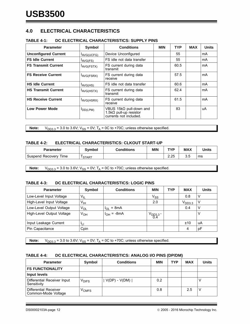
4.0 ELECTRICAL CHARACTERISTICS
TABLE 4-1: DC ELECTRICAL CHARACTERISTICS: SUPPLY PINS
Parameter Symbol Conditions MIN TYP MAX Units
Unconfigured Current IAVG(UCFG) Device Unconfigured 55 mA
FS Idle Current IAVG(FS) FS idle not data transfer 55 mA
FS Transmit Current IAVG(FSTX) FS current during data transmit
60.5 mA
FS Receive Current IAVG(FSRX) FS current during data receive
57.5 mA
HS Idle Current IAVG(HS) FS idle not data transfer 60.6 mA
HS Transmit Current IAVG(HSTX) FS current during data transmit
62.4 mA
HS Receive Current IAVG(HSRX) FS current during data receive
61.5 mA
Low Power Mode IDD(LPM) VBUS 15kΩ pull-down and 1.5kΩ pull-up resistor currents not included.
83 uA
Note: VDD3.3 = 3.0 to 3.6V; VSS = 0V; TA = 0C to +70C; unless otherwise specified.
TABLE 4-2: ELECTRICAL CHARACTERISTICS: CLKOUT START-UP
Parameter Symbol Conditions MIN TYP MAX Units
Suspend Recovery Time TSTART 2.25 3.5 ms
Note: VDD3.3 = 3.0 to 3.6V; VSS = 0V; TA = 0C to +70C; unless otherwise specified.
TABLE 4-3: DC ELECTRICAL CHARACTERISTICS: LOGIC PINS
Parameter Symbol Conditions MIN TYP MAX Units
Low-Level Input Voltage VIL VSS 0.8 V
High-Level Input Voltage VIH 2.0 VDD3.3 V
Low-Level Output Voltage VOL IOL = 8mA 0.4 V
High-Level Output Voltage VOH IOH = -8mA VDD3.3 - 0.4
V
Input Leakage Current ILI ±10 uA
Pin Capacitance Cpin 4 pF
Note: VDD3.3 = 3.0 to 3.6V; VSS = 0V; TA = 0C to +70C; unless otherwise specified.
TABLE 4-4: DC ELECTRICAL CHARACTERISTICS: ANALOG I/O PINS (DP/DM)
Parameter Symbol Conditions MIN TYP MAX Units
FS FUNCTIONALITY
Input levels
Differential Receiver Input Sensitivity
VDIFS | V(DP) - V(DM) | 0.2 V
Differential ReceiverCommon-Mode Voltage
VCMFS 0.8 2.5 V
DS00002103A-page 12 2005 - 2016 Microchip Technology Inc.

USB3500
Single-Ended Receiver Low Level Input Voltage
VILSE 0.8 V
Single-Ended Receiver High Level Input Voltage
VIHSE 2.0 V
Single-Ended Receiver Hysteresis
VHYSSE 0.050 0.150 V
Output Levels
Low Level Output Voltage VFSOL Pull-up resistor on DP;RL = 1.5kΩ to VDD3.3
0.3 V
High Level Output Voltage VFSOH Pull-down resistor on DP, DM;RL = 15kΩ to GND
2.8 3.6 V
Termination
Driver Output Impedance forHS and FS
ZHSDRV Steady state drive 40.5 45 49.5 Ω
Input Impedance ZINP TX, RPU disabled 1.0 MΩ
Pull-up Resistor Impedance ZPU Bus Idle 0.900 1.24 1.575 kΩ
Pull-up Resistor Impedance ZPURX Device Receiving 1.425 2.26 3.09 kΩ
Pull-dn Resistor Impedance ZPD 14.25 15.0 15.75 kΩ
HS FUNCTIONALITY
Input levels
HS Differential Input Sensitivity VDIHS | V(DP) - V(DM) | 100 mV
HS Data Signaling CommonMode Voltage Range
VCMHS -50 500 mV
HS Squelch Detection Threshold (Differential) VHSSQ
Squelch Threshold 100 mV
Un-squelch Threshold 150 mV
Output Levels
Hi-Speed Low LevelOutput Voltage (DP/DMreferenced to GND)
VHSOL 45Ω load -10 10 mV
Hi-Speed High LevelOutput Voltage (DP/DMreferenced to GND)
VHSOH 45Ω load 360 440 mV
Hi-Speed IDLE LevelOutput Voltage (DP/DMreferenced to GND)
VOLHS 45Ω load -10 10 mV
Chirp-J Output Voltage (Differential)
VCHIRPJ HS termination resistor disabled, pull-up resistor connected. 45Ω load.
700 1100 mV
Chirp-K Output Voltage(Differential)
VCHIRPK HS termination resistor disabled, pull-up resistor connected. 45Ω load.
-900 -500 mV
Leakage Current
OFF-State Leakage Current ILZ ±10 uA
Port Capacitance
Transceiver Input Capacitance CIN Pin to GND 5 10 pF
Note: VDD3.3 = 3.0 to 3.6V; VSS = 0V; TA = 0C to +70C; unless otherwise specified.
TABLE 4-4: DC ELECTRICAL CHARACTERISTICS: ANALOG I/O PINS (DP/DM) (CONTINUED)
Parameter Symbol Conditions MIN TYP MAX Units
2005 - 2016 Microchip Technology Inc. DS00002103A-page 13

USB3500
TABLE 4-5: DYNAMIC CHARACTERISTICS: ANALOG I/O PINS (DP/DM)
Parameter Symbol Conditions MIN TYP MAX Units
FS Output Driver Timing
Rise Time TFSR CL = 50pF; 10 to 90% of|VOH - VOL|
4 20 ns
Fall Time TFFF CL = 50pF; 10 to 90% of|VOH - VOL|
4 20 ns
Output Signal Crossover Voltage
VCRS Excluding the first transition from IDLE state
1.3 2.0 V
Differential Rise/Fall Time Matching
FRFM Excluding the first transition from IDLE state
90 111.1 %
HS Output Driver Timing
Differential Rise Time THSR 500 ps
Differential Fall Time THSF 500 ps
Driver Waveform Requirements
Eye pattern of Template 1 in USB 2.0 specification
Hi-Speed Mode Timing
Receiver Waveform Requirements
Eye pattern of Template 4 in USB 2.0 specification
Data Source Jitter and Receiver Jitter Tolerance
Eye pattern of Template 4 in USB 2.0 specification
Note: VDD3.3 = 3.0 to 3.6V; VSS = 0V; TA = 0C to +70C; unless otherwise specified.
TABLE 4-6: DYNAMIC CHARACTERISTICS: DIGITAL UTMI PINS
Parameter Symbol Conditions MIN TYP MAX Units
UTMI Timing
DATA[7:0] TPD Output Delay. Measured from PHY output to the rising edge of CLKOUT
2 5 ns
RXVALID
RXACTIVE
RXERROR
LINESTATE[1:0]
TXREADY
DATA[7:0] TSU Setup Time. Measured from PHY input to the rising edge of CLKOUT.
5 1 ns
TXVALID
OPMODE[1:0]
XCVRSELECT[1:0]
TERMSELECT
DATA[7:0] TH Hold time. Measured from the rising edge of CLKOUT to the PHY input signal edge.
0 ns
TXVALID
OPMODE[1:0]
XCVRSELECT[1:0]
TERMSELECT
Note: VDD3.3 = 3.0 to 3.6V; VSS = 0V; TA = 0C to +70C; unless otherwise specified.
DS00002103A-page 14 2005 - 2016 Microchip Technology Inc.

USB3500
TABLE 4-7: OTG ELECTRICAL CHARACTERISTICS
Parameter Symbol Conditions MIN TYP MAX Units
SessEnd trip point VSessEnd 0.2 0.5 0.8 V
SessVld trip point VSessVld 0.8 1.4 2.0 V
VBUSVld trip point VVbusVld 4.4 4.58 4.75 V
Vbus Pull-Up RVbusPu Vbus to VDD3.3 (CHRGVBUS = 1)
281 340 Ω
Vbus Pull-down RVbusPd Vbus to GND (DISCHRGVBUS = 1)
656 850 Ω
Vbus Impedance RVbus Vbus to GND 40 75 100 kΩ
ID pull-up resistance RIdPullUp (IDOULLUP = 1) 80 100 120 kΩ
ID pull-up resistance RId (IDPULLUP = 0) 1 MΩ
Note: VDD3.3 = 3.0 to 3.6V; VSS = 0V; TA = 0C to +70C; unless otherwise specified.
TABLE 4-8: REGULATOR OUTPUT VOLTAGES
Parameter Symbol Conditions MIN TYP MAX Units
VDDA1.8 VDDA1.8 Normal Operation (SUSPENDN = 1)
1.6 1.8 2.0 V
VDDA1.8 VDDA1.8 Low Power mode(SUSPENDN = 0)
0 V
VDD1.8 VDD1.8 1.6 1.8 2.0 V
Note: VDD3.3 = 3.0 to 3.6V; VSS = 0V; TA = 0C to +70C; unless otherwise specified.
2005 - 2016 Microchip Technology Inc. DS00002103A-page 15

USB3500
5.0 DETAILED FUNCTIONAL DESCRIPTION
FIGURE 2-1: on page 5 shows the functional block diagram of the USB3500. Each of the functions is described in detailbelow.
5.1 8bit Bi-Directional Data Bus Operation
The USB3500 supports an 8-bit bi-directional parallel interface.
• CLKOUT runs at 60MHz
• The 8-bit data bus (DATA[7:0]) is used for transmit when TXVALID = 1
• The 8-bit data bus (DATA[7:0]) is used for receive when TXVALID = 0
Figure 5-1 shows the relationship between CLKOUT and the transmit data transfer signals in FS mode. TXREADY isonly asserted for one CLKOUT per byte time to signal the Link that the data on the DATA lines has been read by thePHY. The Link may hold the data on the DATA lines for the duration of the byte time. Transitions of TXVALID must meetthe defined setup and hold times relative to CLKOUT.
Figure 5-2 shows the relationship between CLKOUT and the receive data control signals in FS mode. RXACTIVE“frames” a packet, transitioning only at the beginning and end of a packet. However transitions of RXVALID may takeplace any time 8 bits of data are available. Figure 5-2 also shows how RXVALID is only asserted for one CLKOUT cycleper byte time even though the data may be presented for the full byte time. The XCVRSELECT signal determineswhether the HS or FS timing relationship is applied to the data and control signals.
FIGURE 5-1: FS CLK RELATIONSHIP TO TRANSMIT DATA AND CONTROL SIGNALS
FIGURE 5-2: FS CLK RELATIONSHIP TO RECEIVE DATA AND CONTROL SIGNALS
DS00002103A-page 16 2005 - 2016 Microchip Technology Inc.

USB3500
5.2 TX Logic
This block receives parallel data bytes placed on the DATA bus and performs the necessary transmit operations. Theseoperations include parallel to serial conversion, bit stuffing and NRZI encoding. Upon valid assertion of the proper TXcontrol lines by the Link and TX State Machine, the TX LOGIC block will synchronously shift, at either the FS or HS rate,the data to the FS/HS TX block to be transmitted on the USB cable. Data transmit timing is shown in Figure 5-3.
The behavior of the Transmit State Machine is described below.
• The Link asserts TXVALID to begin a transmission.
• After the Link asserts TXVALID it can assume that the transmission has started when it detects TXREADY has been asserted.
• The Link must assume that the USB3500 has consumed a data byte if TXREADY and TXVALID are asserted on the rising edge of CLKOUT.
• The Link must have valid packet information (PID) asserted on the DATA bus coincident with the assertion of TXVALID.
• TXREADY is sampled by the Link on the rising edge of CLKOUT.
• The Link negates TXVALID to complete a packet. Once negated, the transmit logic will never reassert TXREADY until after the EOP has been generated. (TXREADY will not re-assert until TXVALD asserts again.)
• The USB3500 is ready to transmit another packet immediately. However, the Link must conform to the minimum inter-packet delays identified in the USB 2.0 specification.
• Supports high speed disconnect detect through the HOSTDISC pin. In Host mode the USB3500 will sample the disconnect comparator at the 32nd bit of the 40 bit long EOP during SOF packets.
• Supports FS pre-amble for FS hubs with a LS device.
• Supports LS keep alive by receiving the SOF PID.
• Supports Host mode resume K which ends with two low speed times of SE0 followed by 1 FS “J”.
FIGURE 5-3: TRANSMIT TIMING FOR A DATA PACKET
2005 - 2016 Microchip Technology Inc. DS00002103A-page 17

USB3500
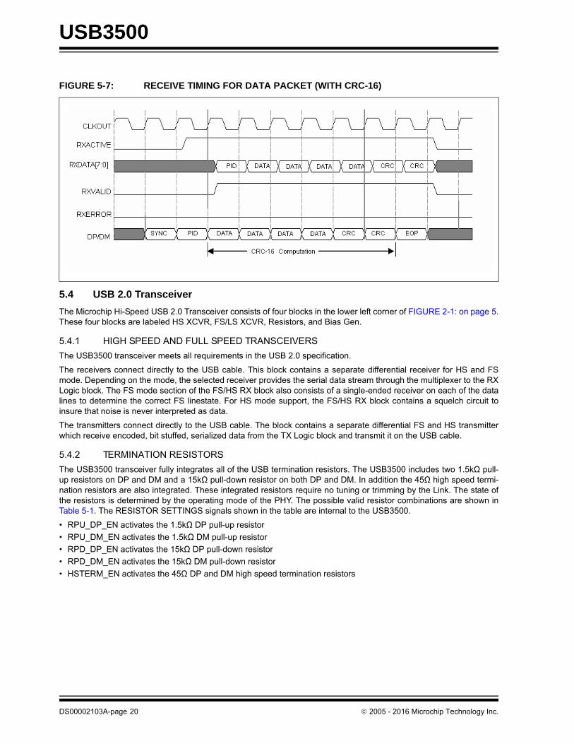
5.3 RX Logic
This block receives serial data from the clock recovery circuits and processes it to be transferred to the Link on the DATAbus. The processing involved includes NRZI decoding, bit unstuffing, and serial to parallel conversion. Upon valid asser-tion of the proper RX control lines, the RX Logic block will provide bytes to the DATA bus as shown in the figures below.The behavior of the receiver is described below.
The assertion of RESET will cause the USB3500 to deasserts RXACTIVE and RXVALID. When the RESET signal isdeasserted the Receive State Machine starts looking for a SYNC pattern on the USB. When a SYNC pattern is detected,the receiver will assert RXACTIVE. The length of the received Hi-Speed SYNC pattern varies and can be up to 32 bitslong or as short as 12 bits long when at the end of five hubs.
After valid serial data is received, the data is loaded into the RX Holding Register on the rising edge of CLKOUT, andRXVALID is asserted. The Link must read the DATA bus on the next rising edge of CLKOUT. In normal mode (OPMODE= 00), then stuffed bits are stripped from the data stream. Each time 8 stuffed bits are accumulated the USB3500 willnegate RXVALID for one clock cycle, thus skipping a byte time.
When the EOP is detected the USB3500 will negate RXACTIVE and RXVALID. After the EOP has been stripped, theUSB3500 will begin looking for the next packet.
The behavior of the USB3500 receiver is described below:
• RXACTIVE and RXREADY are sampled on the rising edge of CLKOUT.
• After a EOP is complete the receiver will begin looking for SYNC.
• The USB3500 asserts RXACTIVE when SYNC is detected.
• The USB3500 negates RXACTIVE when an EOP is detected and the elasticity buffer is empty.
• When RXACTIVE is asserted, RXVALID will be asserted if the RX Holding Register is full.
• RXVALID will be negated if the RX Holding Register was not loaded during the previous byte time. This will occur if 8 stuffed bits have been accumulated.
• The Link must be ready to consume a data byte if RXACTIVE and RXVALID are asserted (RX Data state).
• Figure 5-5 shows the timing relationship between the received data (DP/DM), RXVALID, RXACTIVE, RXERROR and DATA signals.
FIGURE 5-4: RECEIVE TIMING FOR DATA WITH UNSTUFFED BITS
Note:
• Figure 5-5, Figure 5-6 and Figure 5-7 are timing examples of a HS/FS PHY when it is in HS mode. When a HS/FS PHY is in FS Mode there are approximately 40 CLKOUT cycles every byte time. The Receive State Machine assumes that the Link captures the data on the DATA bus if RXACTIVE and RXVALID are asserted. In FS mode, RXVALID will only be asserted for one CLKOUT per byte time.
• In Figure 5-5, Figure 5-6 and Figure 5-7 the SYNC pattern on DP/DM is shown as one byte long. The SYNC pat-tern received by a device can vary in length. These figures assume that all but the last 12 bits have been con-sumed by the hubs between the device and the host controller.
DS00002103A-page 18 2005 - 2016 Microchip Technology Inc.

USB3500
FIGURE 5-5: RECEIVE TIMING FOR A HANDSHAKE PACKET (NO CRC)
FIGURE 5-6: RECEIVE TIMING FOR SETUP PACKET
2005 - 2016 Microchip Technology Inc. DS00002103A-page 19
USB3500
5.4 USB 2.0 Transceiver
The Microchip Hi-Speed USB 2.0 Transceiver consists of four blocks in the lower left corner of FIGURE 2-1: on page 5.These four blocks are labeled HS XCVR, FS/LS XCVR, Resistors, and Bias Gen.
5.4.1 HIGH SPEED AND FULL SPEED TRANSCEIVERS
The USB3500 transceiver meets all requirements in the USB 2.0 specification.
The receivers connect directly to the USB cable. This block contains a separate differential receiver for HS and FSmode. Depending on the mode, the selected receiver provides the serial data stream through the multiplexer to the RXLogic block. The FS mode section of the FS/HS RX block also consists of a single-ended receiver on each of the datalines to determine the correct FS linestate. For HS mode support, the FS/HS RX block contains a squelch circuit toinsure that noise is never interpreted as data.
The transmitters connect directly to the USB cable. The block contains a separate differential FS and HS transmitterwhich receive encoded, bit stuffed, serialized data from the TX Logic block and transmit it on the USB cable.
5.4.2 TERMINATION RESISTORS
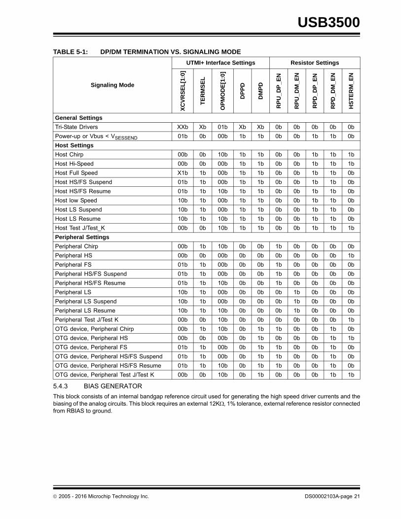
The USB3500 transceiver fully integrates all of the USB termination resistors. The USB3500 includes two 1.5kΩ pull-up resistors on DP and DM and a 15kΩ pull-down resistor on both DP and DM. In addition the 45Ω high speed termi-nation resistors are also integrated. These integrated resistors require no tuning or trimming by the Link. The state ofthe resistors is determined by the operating mode of the PHY. The possible valid resistor combinations are shown inTable 5-1. The RESISTOR SETTINGS signals shown in the table are internal to the USB3500.
• RPU_DP_EN activates the 1.5kΩ DP pull-up resistor
• RPU_DM_EN activates the 1.5kΩ DM pull-up resistor
• RPD_DP_EN activates the 15kΩ DP pull-down resistor
• RPD_DM_EN activates the 15kΩ DM pull-down resistor
• HSTERM_EN activates the 45Ω DP and DM high speed termination resistors
FIGURE 5-7: RECEIVE TIMING FOR DATA PACKET (WITH CRC-16)
DS00002103A-page 20 2005 - 2016 Microchip Technology Inc.
USB3500
5.4.3 BIAS GENERATOR
This block consists of an internal bandgap reference circuit used for generating the high speed driver currents and thebiasing of the analog circuits. This block requires an external 12K, 1% tolerance, external reference resistor connectedfrom RBIAS to ground.
TABLE 5-1: DP/DM TERMINATION VS. SIGNALING MODE
Signaling Mode
UTMI+ Interface Settings Resistor Settings
XC
VR
SE
L[1
:0]
TE
RM
SE
L
OP
MO
DE
[1:0
]
DP
PD
DM
PD
RP
U_
DP
_EN
RP
U_D
M_E
N
RP
D_
DP
_E
N
RP
D_D
M_E
N
HS
TE
RM
_EN
General Settings
Tri-State Drivers XXb Xb 01b Xb Xb 0b 0b 0b 0b 0b
Power-up or Vbus < VSESSEND 01b 0b 00b 1b 1b 0b 0b 1b 1b 0b
Host Settings
Host Chirp 00b 0b 10b 1b 1b 0b 0b 1b 1b 1b
Host Hi-Speed 00b 0b 00b 1b 1b 0b 0b 1b 1b 1b
Host Full Speed X1b 1b 00b 1b 1b 0b 0b 1b 1b 0b
Host HS/FS Suspend 01b 1b 00b 1b 1b 0b 0b 1b 1b 0b
Host HS/FS Resume 01b 1b 10b 1b 1b 0b 0b 1b 1b 0b
Host low Speed 10b 1b 00b 1b 1b 0b 0b 1b 1b 0b
Host LS Suspend 10b 1b 00b 1b 1b 0b 0b 1b 1b 0b
Host LS Resume 10b 1b 10b 1b 1b 0b 0b 1b 1b 0b
Host Test J/Test_K 00b 0b 10b 1b 1b 0b 0b 1b 1b 1b
Peripheral Settings
Peripheral Chirp 00b 1b 10b 0b 0b 1b 0b 0b 0b 0b
Peripheral HS 00b 0b 00b 0b 0b 0b 0b 0b 0b 1b
Peripheral FS 01b 1b 00b 0b 0b 1b 0b 0b 0b 0b
Peripheral HS/FS Suspend 01b 1b 00b 0b 0b 1b 0b 0b 0b 0b
Peripheral HS/FS Resume 01b 1b 10b 0b 0b 1b 0b 0b 0b 0b
Peripheral LS 10b 1b 00b 0b 0b 0b 1b 0b 0b 0b
Peripheral LS Suspend 10b 1b 00b 0b 0b 0b 1b 0b 0b 0b
Peripheral LS Resume 10b 1b 10b 0b 0b 0b 1b 0b 0b 0b
Peripheral Test J/Test K 00b 0b 10b 0b 0b 0b 0b 0b 0b 1b
OTG device, Peripheral Chirp 00b 1b 10b 0b 1b 1b 0b 0b 1b 0b
OTG device, Peripheral HS 00b 0b 00b 0b 1b 0b 0b 0b 1b 1b
OTG device, Peripheral FS 01b 1b 00b 0b 1b 1b 0b 0b 1b 0b
OTG device, Peripheral HS/FS Suspend 01b 1b 00b 0b 1b 1b 0b 0b 1b 0b
OTG device, Peripheral HS/FS Resume 01b 1b 10b 0b 1b 1b 0b 0b 1b 0b
OTG device, Peripheral Test J/Test K 00b 0b 10b 0b 1b 0b 0b 0b 1b 1b
2005 - 2016 Microchip Technology Inc. DS00002103A-page 21

USB3500
5.5 Crystal Oscillator and PLL
The USB3500 uses an internal crystal driver and PLL sub-system to provide a clean 480MHz reference clock that isused by the PHY during both transmit and receive. The USB3500 requires a clean 24MHz crystal or clock as a frequencyreference. If the 24MHz reference is noisy or off frequency the PHY may not operate correctly.
The USB3500 can use either a crystal or an external clock oscillator for the 24MHz reference. The crystal is connectedto the XI and XO pins as shown in the application diagram, Figure 6-10. If a clock oscillator is used, the clock should beconnected to the XI input and the XO pin left floating. When using an external clock, the clock source must be clean soit does not degrade performance, and should be driven with a 0 to 3.3 volt signal.
After the 480MHz PLL has locked to the correct frequency, it will drive the CLKOUT pin with a 60MHz clock. TheUSB3500 is ensured to start the clock within the time specified in Table 4-2.
5.6 Internal Regulators and POR
The USB3500 includes integrated power management functions to reduce the bill of materials and simplify productdesign.
5.6.1 INTERNAL REGULATORS
The USB3500 has two internal regulators that create two 1.8V outputs (labeled VDD1.8 and VDDA1.8) from the 3.3 voltpower supply input (VDD3.3). Each regulator requires an external 4.7uF +/-20% low ESR bypass capacitor to ensurestability. X5R or X7R ceramic capacitors are recommended since they exhibit an ESR lower that 0.1ohm at frequenciesgreater than 10kHz.
The specific capacitor recommendations for each pin are detailed in Table 2.1, "USB3500 Pin Locations", and shown inFigure 6-10, "USB3500 Application Diagram (Top View)".
5.6.2 POWER ON RESET (POR)
The USB3500 provides an internal POR circuit that generates a reset pulse once the PHY supplies are stable. TheUTMI+ Digital can be reset at any time with the RESET pin.
5.7 USB On-The-Go (OTG) Module
The USB3500 provides support for USB OTG. This mode allows the USB3500 to be dynamically configured as a hostor a device depending on the type of cable inserted into the Mini-AB connector. When the Mini-A plug of a cable isinserted into the Mini-AB connector the USB device becomes the A-device. When a Mini-B plug is inserted the devicebecomes the B-device. The OTG A-device behaves similar to a Host while the B-device behaves similar to a peripheral.The differences are covered in the OTG supplement.
The OTG Module meets all the requirements in the “On-The-Go Supplement to the USB 2.0 Specification”. In applica-tions where only Host or Device is required, the OTG Module is unused.
Note: The USB3500 regulators are designed to generate a 1.8volt supply for the USB3500 only. Using the reg-ulators to provide current for other circuits is not recommended and Microchip does not ensure USB per-formance or regulator stability in this case.
DS00002103A-page 22 2005 - 2016 Microchip Technology Inc.

USB3500
The OTG Module can be broken into 4 main blocks; ID Detection, VBUS Control, Driving External VBUS, and ExternalVBUS Detection. Each of these blocks is covered in the sections below.
5.7.1 ID DETECTION
The USB3500 provides an ID pin to determine the type of USB cable connected. When the Mini-A Plug of a USB cableis inserted into the Mini-AB connector, the ID pin is shorted to ground. When the Mini-B Plug is inserted into the Mini-AB connector, the ID pin is allowed to float.
The USB3500 provides an integrated pull-up resistor to pull the ID pin to VDD3.3 when a Mini-B plug is inserted andthe cable is floating. When a Mini-A plug is connected, the pull-up resistor will be overpowered and the ID pin will bebrought to ground. To save current when a Mini-A Plug is inserted, the ID pull-up resistor can be disabled by clearingthe IDPULLUP pin. To prevent the ID pin from floating to a random value, a weak pull-up resistor is provided at all times.The circuits related to the ID comparator are shown in Figure 5-8 and their related parameters are shown in Table 4-7.
FIGURE 5-8: USB3500 ON-THE-GO MODULE
TABLE 5-2: IDGND VS. USB CABLE TYPE
USB Plug OTG Role ID Voltage IDGND
A HOST 0 0
B PERIPHERAL 3.3 1
R=
75K
R>
=65
6R
>=
281
OTG Module
VBUS
ID
VDD33
VBUSVLD
SESSVLD
SESSEND
IDPULLUP
DISCHRGVBUS
ID_DIG
CHRGVBUS
0.5V
1.4V
4.575V
0.6V
R=
100
K
R>
1M
2005 - 2016 Microchip Technology Inc. DS00002103A-page 23

USB3500
5.7.2 VBUS CONTROL
The USB3500 includes all of the Vbus comparators required for OTG. The VbusVld, SessVld, and SessEnd compara-tors are fully integrated into the USB3500. These comparators are used to ensure the Vbus voltage is the correct valuefor proper USB operation.
The VbusVld comparator is used by the Link, when configured as an A device, to ensure that the Vbus voltage on thecable is valid. The SessVld comparator is used by the Link when configured as either an A or B device to indicate asession is requested or valid. Finally the SessEnd comparator is used by the B-device to indicate a USB session hasended.
Also included in the VBUS Control block are the resistors used for VBUS pulsing in SRP. The resistors used for VBUSpulsing include a pull-down to ground and a pull-up to VDD3.3.
5.7.2.1 SessEnd Comparator
The SessEnd comparator is designed to trip when Vbus is less than 0.5 volts. When Vbus goes below 0.5 volts, thesession is considered to be ended and SessEnd will transition from 0 to 1. The SessEnd comparator is disabled whenthe Suspendn = 0. When disabled, the SessEnd output is 0. The SessEnd comparator trip points are detailed in Table 4-7.
5.7.2.2 SessVld Comparator
The SessVld comparator is used when the PHY is configured as either an A or B device. When configured as an Adevice, the SessVld is used to detect Session Request protocol (SRP). When configured as a B device, SessVld is usedto detect the presence of Vbus. The SessVld comparator is not disabled with Suspendn and its output will always reflectthe state of VBUS. The SessVld comparator trip point is detailed in Table 4-7.
5.7.2.3 VbusVld Comparator
The final Vbus comparator is the VbusVld comparator. This comparator is only used when configured as an A-device.In the OTG protocol the A-device is responsible to ensure that the VBUS voltage is within a certain range. The VbusVldcomparator is disabled when Suspendn = 0. When disabled the VbusVld will read 0. The VbusVld comparator trip pointsare detailed in Table 4-7.
When the A-device is able to provide 8-100mA, it must ensure Vbus doesn’t go below 4.4 volts. If the A-device can pro-vide 100-500mA on VBUS, it must ensure that Vbus does not go below 4.75 volts.
The internal Vbus comparator is designed to ensure that Vbus remains above 4.4 volts. If the design is required to sup-ply over 100mA an external Vbus comparator or overcurrent fault detection should be used.
5.7.2.4 Vbus Pull-up and Pull-down Resistors
In addition to the internal Vbus comparators, the USB3500 also includes the integrated VBUS pull-up and pull-downresistors used for VBUS Pulsing. To discharge the VBUS voltage, so that a Session Request can begin, the USB3500provides a pull-down resistor from VBUS to Ground. This resistor is controlled by the DISCHRGVBUS pin. The pull-upresistor is connected between VBUS and VDD3.3. This resistor is used to pull Vbus above 2.1 volts to indicate to theA-Device that a USB session has been requested. The state of the pull-up resistor is controlled by the CHRGVBUS pin.The Pull-Up and Pull-Down resistor values are detailed in Table 4-7.
5.7.2.5 Vbus Input Impedance
The OTG Supplement requires an A-Device that supports Session request protocol to have an input impedance lessthan 100kohm and greater the 40kohm to ground. In addition, if configured as a B-Device, the PHY cannot draw morethen 150uA from Vbus. The USB3500 provides a 75kΩ nominal resistance to ground which meets the above require-ments.
Note: The OTG Supplement specifies a voltage range for A-Device Session Valid and B-Device Session Validcomparator. The USB3500 PHY combines the two comparators into one and uses the narrower thresholdrange.
DS00002103A-page 24 2005 - 2016 Microchip Technology Inc.

USB3500
6.0 APPLICATION NOTES
The following sections consist of select functional explanations to aid in implementing the USB3500 into a system. Forcomplete description and specifications consult the USB 2.0 Transceiver Macrocell Interface Specification and Univer-sal Serial Bus Specification Revision 2.0.
6.1 Linestate
The voltage thresholds that the LINESTATE[1:0] signals use to reflect the state of DP and DM depend on the state ofXCVRSELECT. LINESTATE[1:0] uses HS thresholds when the HS transceiver is enabled (XCVRSELECT = 0) and FSthresholds when the FS transceiver is enabled (XCVRSELECT = 1). There is not a concept of variable single-endedthresholds in the USB 2.0 specification for HS mode.
The HS receiver is used to detect Chirp J or K, where the output of the HS receiver is always qualified with the Squelchsignal. If squelched, the output of the HS receiver is ignored. In the USB3500, as an alternative to using variable thresh-olds for the single-ended receivers, the following approach is used. In HS device mode, 3ms of no USB activity (IDLEstate) signals a reset. The Link monitors LINESTATE[1:0] for the IDLE state. To minimize transitions on LINESTATE[1:0]while in HS mode, the presence of !Squelch is used to force LINESTATE[1:0] to a J state.
TABLE 6-1: DEVICE LINESTATE STATES (DPPD & DMPD = 0)
State of DP/DM Lines
Linestate[1:0] Full SpeedXCVRSELECT[1:0]=01
TERMSELECT=1
High SpeedXCVRSELECT[1:0]=00
TERMSELECT=0
Chirp ModeXCVRSELECT[1:0]=00
TERMSELECT=1LS[1] LS[0]
0 0 SE0 Squelch Squelch
0 1 FS-J !Squelch !Squelch & HS Differential Receiver
Output
1 0 FS-K Invalid !Squelch &!HS Differential Receiver
Output
1 1 SE1 Invalid Invalid
TABLE 6-2: HOST LINESTATE STATES (DPPD & DMPD = 1)
State of DPDM Lines
Linestate[1:0]Low Speed
XCVRSEL[1:0]=10TERMSELECT=1
Full SpeedXCVRSEL[1:0]=01TERMSELECT=1
High SpeedXCVRSEL[1:0]=00TERMSELECT=0OPMODE=00/01
Chirp ModeXCVRSEL[1:0]=00TERMSELECT=0
OPMODE=10LS[1] LS[0]
0 0 SE0 SE0 Squelch Squelch
0 1 LS-K FS-J !Squelch !Squelch & HS Differential
Receiver Output
1 0 LS-J FS-K Invalid !Squelch &!HS Differential Receiver Output
1 1 SE1 SE1 Invalid Invalid
2005 - 2016 Microchip Technology Inc. DS00002103A-page 25

USB3500
6.2 OPMODES
The OPMODE[1:0] pins allow control of the operating modes.
The OPMODE[1:0] signals are normally changed only when the transmitter and the receiver are quiescent, i.e. whenentering a test mode or for a device initiated resume.
When using OPMODE[1:0] = 10, the SYNC and EOP patterns are not transmitted.
The only exception to this is when OPMODE[1:0] is set to 10 while TXVALID has been asserted (the transceiver is trans-mitting a packet), in order to flag a transmission error. In this case, the USB3500 has already transmitted the SYNCpattern so upon negation of TXVALID the EOP must also be transmitted to properly terminate the packet. Changing theOPMODE[1:0] signals under all other conditions (while the transceiver is transmitting or receiving data) will generateundefined results.
6.3 Test Mode Support
6.4 SE0 Handling
For FS operation, IDLE is a J state on the bus. SE0 is used as part of the EOP or to indicate reset. When asserted inan EOP, SE0 is never asserted for more than 2 bit times. The assertion of SE0 for more than 2.5us is interpreted as areset by the device operating in FS mode.
For HS operation, IDLE is a SE0 state on the bus. SE0 is also used to reset a HS device. A HS device cannot use the2.5us assertion of SE0 (as defined for FS operation) to indicate reset since the bus is often in this state between packets.If no bus activity (IDLE) is detected for more than 3ms, a HS device must determine whether the downstream facingport is signaling a suspend or a reset. The following section details how this determination is made. If a reset is signaled,the HS device will then initiate the HS Detection Handshake protocol.
TABLE 6-3: OPERATIONAL MODES
Mode[1:0] State Name Description
00 Normal Operation Transceiver operates with normal USB data encoding and decoding
01 Non-Driving Allows the transceiver logic to support a soft disconnect feature which tri-states both the HS and FS transmitters, and removes any termination from the USB making it appear to an upstream port that the device has been disconnected from the bus
10 Disable Bit Stuffing and NRZI encoding
Disables bitstuffing and NRZI encoding logic so that 1's loaded from the DATA bus become 'J's on the DP/DM and 0's become 'K's
11 Reserved N/A
TABLE 6-4: USB 2.0 TEST MODES
USB 2.0 Test Modes
USB3500 Setup
Operational Mode Link Transmitted DataXCVRSELECT & TERMSELECT
SE0_NAK State 0 No transmit HS
J State 2 All '1's HS
K State 2 All '0's HS
Test_Packet State 0 Test Packet data HS
DS00002103A-page 26 2005 - 2016 Microchip Technology Inc.
USB3500
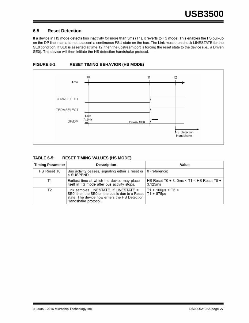
6.5 Reset Detection
If a device in HS mode detects bus inactivity for more than 3ms (T1), it reverts to FS mode. This enables the FS pull-upon the DP line in an attempt to assert a continuous FS J state on the bus. The Link must then check LINESTATE for theSE0 condition. If SE0 is asserted at time T2, then the upstream port is forcing the reset state to the device (i.e., a DrivenSE0). The device will then initiate the HS detection handshake protocol.
FIGURE 6-1: RESET TIMING BEHAVIOR (HS MODE)
TABLE 6-5: RESET TIMING VALUES (HS MODE)
Timing Parameter Description Value
HS Reset T0 Bus activity ceases, signaling either a reset or a SUSPEND.
0 (reference)
T1 Earliest time at which the device may place itself in FS mode after bus activity stops.
HS Reset T0 + 3. 0ms < T1 < HS Reset T0 + 3.125ms
T2 Link samples LINESTATE. If LINESTATE = SE0, then the SE0 on the bus is due to a Reset state. The device now enters the HS Detection Handshake protocol.
T1 + 100µs < T2 <T1 + 875µs
2005 - 2016 Microchip Technology Inc. DS00002103A-page 27

USB3500
6.6 Suspend Detection
If a HS device detects SE0 asserted on the bus for more than 3ms (T1), it reverts to FS mode. This enables the FS pull-up on the DP line in an attempt to assert a continuous FS J state on the bus. The Link must then check LINESTATE forthe J condition. If J is asserted at time T2, then the upstream port is asserting a soft SE0 and the USB is in a J stateindicating a suspend condition. By time T4 the device must be fully suspended.
6.7 HS Detection Handshake
The downstream facing port asserting an SE0 state on the bus initiates the HS Detection Handshake.
There are three ways in which a device may enter the HS Handshake Detection process:
1. If the device is suspended and it detects an SE0 state on the bus it may immediately enter the HS handshakedetection process.
2. If the device is in FS mode and an SE0 state is detected for more than 2.5µs. it may enter the HS handshakedetection process.
3. If the device is in HS mode and an SE0 state is detected for more than 3.0ms. it may enter the HS handshakedetection process. In HS mode, a device must first determine whether the SE0 state is signaling a suspend or areset condition. To do this the device reverts to FS mode by placing XCVRSELECT and TERMSELECT into FSmode. The device must not wait more than 3.125ms before the reversion to FS mode. After reverting to FS mode,no less than 100µs and no more than 875µs later the Link must check the LINESTATE signals. If a J state is
FIGURE 6-2: SUSPEND TIMING BEHAVIOR (HS MODE)
TABLE 6-6: SUSPEND TIMING VALUES (HS MODE)
Timing Parameter Description Value
HS Reset T0 End of last bus activity, signaling either a reset or a SUSPEND.
0 (reference)
T1 The time at which the device must place itself in FS mode after bus activity stops.
HS Reset T0 + 3. 0ms < T1 < HS Reset T0 + 3.125ms
T2 Link samples LINESTATE. If LINESTATE = 'J', then the initial SE0 on the bus (T0 - T1) had been due to a Suspend state and the Link remains in HS mode.
T1 + 100 µs < T2 <T1 + 875µs
T3 The earliest time where a device can issue Resume signaling.
HS Reset T0 + 5ms
T4 The latest time that a device must actually be suspended, drawing no more than the suspend current from the bus.
HS Reset T0 + 10ms
DS00002103A-page 28 2005 - 2016 Microchip Technology Inc.

USB3500
detected the device will enter a suspend state. If an SE0 state is detected, then the device will enter the HS Hand-shake detection process.
In each case, the assertion of the SE0 state on the bus initiates the reset. The minimum reset interval is 10ms. Depend-ing on the previous mode that the bus was in, the delay between the initial assertion of the SE0 state and entering theHS Handshake detection can be from 0 to 4ms.
This transceiver design pushes as much of the responsibility for timing events on to the Link as possible, and the Linkrequires a stable CLKOUT signal to perform accurate timing. In case 2 and 3 above, CLKOUT has been running and isstable, however in case 1 the USB3500 is reset from a suspend state, and the internal oscillator and clocks of the trans-ceiver are assumed to be powered down. A device has up to 6ms after the release of SUSPENDN to assert a minimumof a 1ms Chirp K.
6.8 HS Detection Handshake – FS Downstream Facing Port
Upon entering the HS Detection process (T0), XCVRSELECT and TERMSELECT are in FS mode. The DP pull-up isasserted and the HS terminations are disabled. The Link then sets OPMODE to Disable Bit Stuffing and NRZI encoding,XCVRSELECT to HS mode, and begins the transmission of all 0's data, which asserts a HS K (chirp) on the bus (T1).The device chirp must last at least 1.0ms, and must end no later than 7.0ms after HS Reset T0. At time T1 the devicebegins listening for a chirp sequence from the host port.
If the downstream facing port is not HS capable, then the HS K asserted by the device is ignored and the alternatingsequence of HS Chirp K’s and J’s is not generated. If no chirps are detected (T4) by the device, it will enter FS modeby returning XCVRSELECT to FS mode.
FIGURE 6-3: HS DETECTION HANDSHAKE TIMING BEHAVIOR (FS MODE)
2005 - 2016 Microchip Technology Inc. DS00002103A-page 29

USB3500
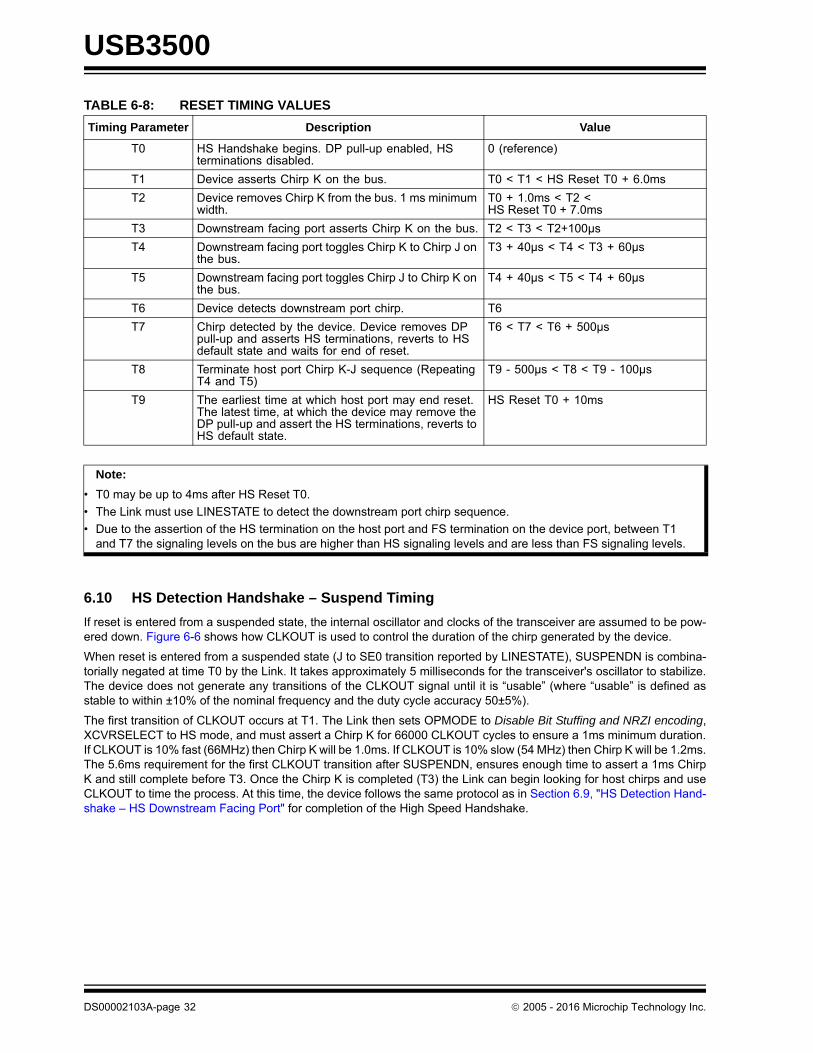
6.9 HS Detection Handshake – HS Downstream Facing Port
Upon entering the HS Detection process (T0), XCVRSELECT and TERMSELECT are in FS mode. The DP pull-up isasserted and the HS terminations are disabled. The Link then sets OPMODE to Disable Bit Stuffing and NRZI encoding,XCVRSELECT to HS mode, and begins the transmission of all 0's data, which asserts a HS K (chirp) on the bus (T1).The device chirp must last at least 1.0ms, and must end no later than 7.0ms after HS Reset T0. At time T1 the devicebegins listening for a chirp sequence from the downstream facing port. If the downstream facing port is HS capable,then it will begin generating an alternating sequence of Chirp K’s and Chirp J’s (T3) after the termination of the chirpfrom the device (T2). After the device sees the valid chirp sequence Chirp K-J-K-J-K-J (T6), it will enter HS mode bysetting TERMSELECT to HS mode (T7).
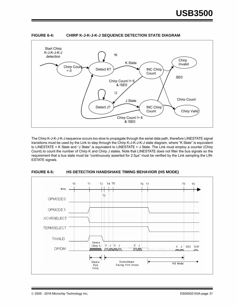
Figure 6-4 provides a state diagram for Chirp K-J-K-J-K-J validation. Prior to the end of reset (T9) the device port mustterminate the sequence of Chirp K’s and Chirp J’s (T8) and assert SE0 (T8-T9). Note that the sequence of Chirp K’sand Chirp J’s constitutes bus activity.
TABLE 6-7: HS DETECTION HANDSHAKE TIMING VALUES (FS MODE)
Timing Parameter
Description Value
T0 HS Handshake begins. DP pull-up enabled, HS terminations disabled.
0 (reference)
T1 Device enables HS Transceiver and asserts Chirp K on the bus.
T0 < T1 < HS Reset T0 + 6.0ms
T2 Device removes Chirp K from the bus. 1ms minimum width.
T1 + 1.0 ms < T2 <HS Reset T0 + 7.0ms
T3 Earliest time when downstream facing port may assert Chirp KJ sequence on the bus.
T2 < T3 < T2+100µs
T4 Chirp not detected by the device. Device reverts to FS default state and waits for end of reset.
T2 + 1.0ms < T4 <T2 + 2.5ms
T5 Earliest time at which host port may end reset HS Reset T0 + 10ms
Note:
• T0 may occur to 4ms after HS Reset T0.
• The Link must assert the Chirp K for 66000 CLKOUT cycles to ensure a 1ms minimum duration.
DS00002103A-page 30 2005 - 2016 Microchip Technology Inc.
USB3500
The Chirp K-J-K-J-K-J sequence occurs too slow to propagate through the serial data path, therefore LINESTATE signaltransitions must be used by the Link to step through the Chirp K-J-K-J-K-J state diagram, where “K State” is equivalentto LINESTATE = K State and “J State” is equivalent to LINESTATE = J State. The Link must employ a counter (ChirpCount) to count the number of Chirp K and Chirp J states. Note that LINESTATE does not filter the bus signals so therequirement that a bus state must be “continuously asserted for 2.5µs” must be verified by the Link sampling the LIN-ESTATE signals.
FIGURE 6-4: CHIRP K-J-K-J-K-J SEQUENCE DETECTION STATE DIAGRAM
FIGURE 6-5: HS DETECTION HANDSHAKE TIMING BEHAVIOR (HS MODE)
Detect K?
Start Chirp K-J-K-J-K-J detection
INC Chirp Count
K State
!K
Detect J?
INC Chirp Count
J State
!J
Chirp Count != 6 & !SE0
Chirp Count = 0
Chirp Count != 6 & !SE0
Chirp Valid
Chirp Invalid
SE0
Chirp Count
2005 - 2016 Microchip Technology Inc. DS00002103A-page 31
USB3500
6.10 HS Detection Handshake – Suspend Timing
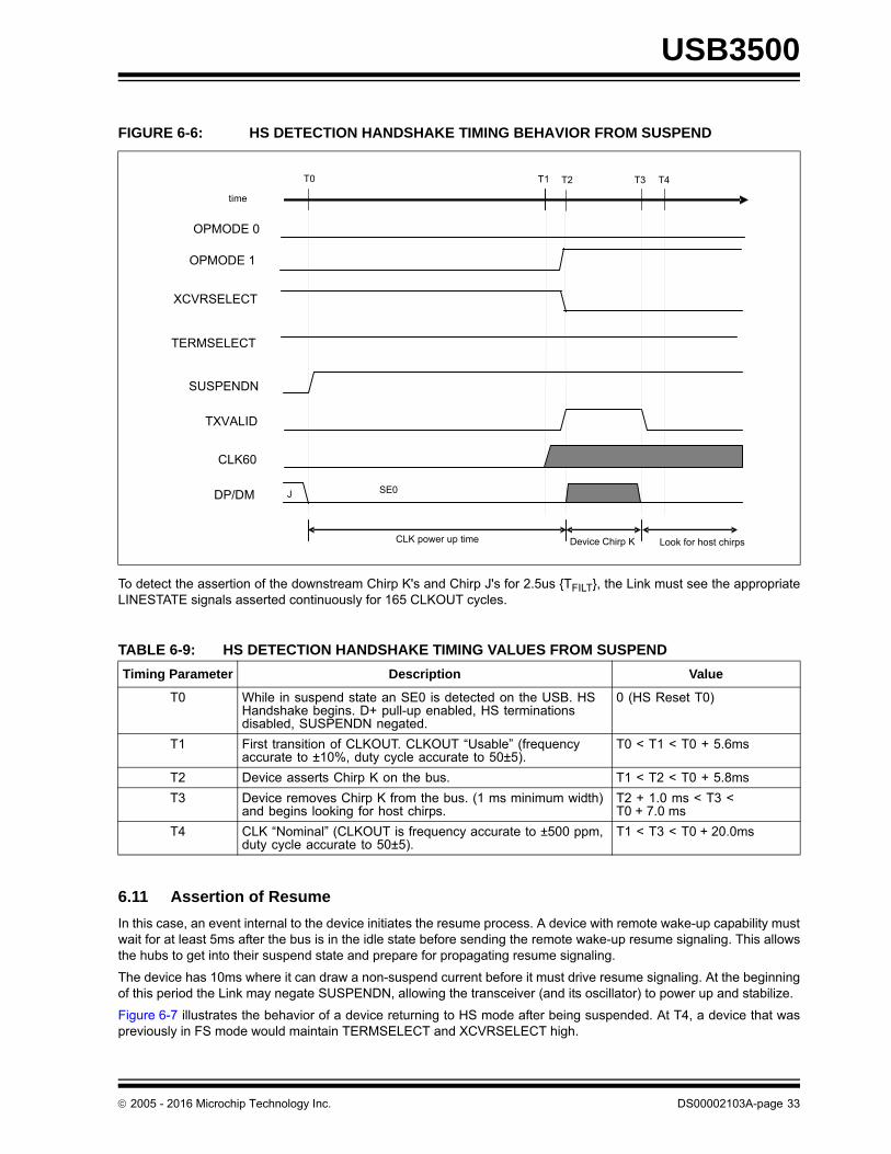
If reset is entered from a suspended state, the internal oscillator and clocks of the transceiver are assumed to be pow-ered down. Figure 6-6 shows how CLKOUT is used to control the duration of the chirp generated by the device.
When reset is entered from a suspended state (J to SE0 transition reported by LINESTATE), SUSPENDN is combina-torially negated at time T0 by the Link. It takes approximately 5 milliseconds for the transceiver's oscillator to stabilize.The device does not generate any transitions of the CLKOUT signal until it is “usable” (where “usable” is defined asstable to within ±10% of the nominal frequency and the duty cycle accuracy 50±5%).
The first transition of CLKOUT occurs at T1. The Link then sets OPMODE to Disable Bit Stuffing and NRZI encoding,XCVRSELECT to HS mode, and must assert a Chirp K for 66000 CLKOUT cycles to ensure a 1ms minimum duration.If CLKOUT is 10% fast (66MHz) then Chirp K will be 1.0ms. If CLKOUT is 10% slow (54 MHz) then Chirp K will be 1.2ms.The 5.6ms requirement for the first CLKOUT transition after SUSPENDN, ensures enough time to assert a 1ms ChirpK and still complete before T3. Once the Chirp K is completed (T3) the Link can begin looking for host chirps and useCLKOUT to time the process. At this time, the device follows the same protocol as in Section 6.9, "HS Detection Hand-shake – HS Downstream Facing Port" for completion of the High Speed Handshake.
TABLE 6-8: RESET TIMING VALUES
Timing Parameter Description Value
T0 HS Handshake begins. DP pull-up enabled, HS terminations disabled.
0 (reference)
T1 Device asserts Chirp K on the bus. T0 < T1 < HS Reset T0 + 6.0ms
T2 Device removes Chirp K from the bus. 1 ms minimum width.
T0 + 1.0ms < T2 < HS Reset T0 + 7.0ms
T3 Downstream facing port asserts Chirp K on the bus. T2 < T3 < T2+100µs
T4 Downstream facing port toggles Chirp K to Chirp J on the bus.
T3 + 40µs < T4 < T3 + 60µs
T5 Downstream facing port toggles Chirp J to Chirp K on the bus.
T4 + 40µs < T5 < T4 + 60µs
T6 Device detects downstream port chirp. T6
T7 Chirp detected by the device. Device removes DP pull-up and asserts HS terminations, reverts to HS default state and waits for end of reset.
T6 < T7 < T6 + 500µs
T8 Terminate host port Chirp K-J sequence (Repeating T4 and T5)
T9 - 500µs < T8 < T9 - 100µs
T9 The earliest time at which host port may end reset. The latest time, at which the device may remove the DP pull-up and assert the HS terminations, reverts to HS default state.
HS Reset T0 + 10ms
Note:
• T0 may be up to 4ms after HS Reset T0.
• The Link must use LINESTATE to detect the downstream port chirp sequence.
• Due to the assertion of the HS termination on the host port and FS termination on the device port, between T1 and T7 the signaling levels on the bus are higher than HS signaling levels and are less than FS signaling levels.
DS00002103A-page 32 2005 - 2016 Microchip Technology Inc.
USB3500
To detect the assertion of the downstream Chirp K's and Chirp J's for 2.5us TFILT, the Link must see the appropriateLINESTATE signals asserted continuously for 165 CLKOUT cycles.
6.11 Assertion of Resume
In this case, an event internal to the device initiates the resume process. A device with remote wake-up capability mustwait for at least 5ms after the bus is in the idle state before sending the remote wake-up resume signaling. This allowsthe hubs to get into their suspend state and prepare for propagating resume signaling.
The device has 10ms where it can draw a non-suspend current before it must drive resume signaling. At the beginningof this period the Link may negate SUSPENDN, allowing the transceiver (and its oscillator) to power up and stabilize.
Figure 6-7 illustrates the behavior of a device returning to HS mode after being suspended. At T4, a device that waspreviously in FS mode would maintain TERMSELECT and XCVRSELECT high.
FIGURE 6-6: HS DETECTION HANDSHAKE TIMING BEHAVIOR FROM SUSPEND
TABLE 6-9: HS DETECTION HANDSHAKE TIMING VALUES FROM SUSPEND
Timing Parameter Description Value
T0 While in suspend state an SE0 is detected on the USB. HS Handshake begins. D+ pull-up enabled, HS terminations disabled, SUSPENDN negated.
0 (HS Reset T0)
T1 First transition of CLKOUT. CLKOUT “Usable” (frequency accurate to ±10%, duty cycle accurate to 50±5).
T0 < T1 < T0 + 5.6ms
T2 Device asserts Chirp K on the bus. T1 < T2 < T0 + 5.8ms
T3 Device removes Chirp K from the bus. (1 ms minimum width) and begins looking for host chirps.
T2 + 1.0 ms < T3 < T0 + 7.0 ms
T4 CLK “Nominal” (CLKOUT is frequency accurate to ±500 ppm, duty cycle accurate to 50±5).
T1 < T3 < T0 + 20.0ms
CLK60
Look for host chirpsDevice Chirp K
SUSPENDN
DP/DM
TERMSELECT
TXVALID
SE0J
CLK power up time
XCVRSELECT
OPMODE 1
OPMODE 0
time
T0 T3 T4T1 T2
2005 - 2016 Microchip Technology Inc. DS00002103A-page 33
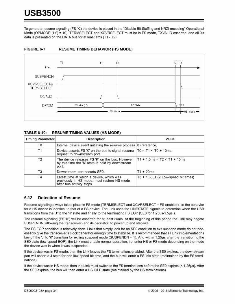
USB3500
To generate resume signaling (FS 'K') the device is placed in the “Disable Bit Stuffing and NRZI encoding” OperationalMode (OPMODE [1:0] = 10), TERMSELECT and XCVRSELECT must be in FS mode, TXVALID asserted, and all 0'sdata is presented on the DATA bus for at least 1ms (T1 - T2).
6.12 Detection of Resume
Resume signaling always takes place in FS mode (TERMSELECT and XCVRSELECT = FS enabled), so the behaviorfor a HS device is identical to that of a FS device. The Link uses the LINESTATE signals to determine when the USBtransitions from the 'J' to the 'K' state and finally to the terminating FS EOP (SE0 for 1.25us-1.5µs.).
The resume signaling (FS 'K') will be asserted for at least 20ms. At the beginning of this period the Link may negateSUSPENDN, allowing the transceiver (and its oscillator) to power up and stabilize.
The FS EOP condition is relatively short. Links that simply look for an SE0 condition to exit suspend mode do not nec-essarily give the transceiver’s clock generator enough time to stabilize. It is recommended that all Link implementationskey off the 'J' to 'K' transition for exiting suspend mode (SUSPENDN = 1). And within 1.25µs after the transition to theSE0 state (low-speed EOP), the Link must enable normal operation, i.e. enter HS or FS mode depending on the modethe device was in when it was suspended.
If the device was in FS mode: then the Link leaves the FS terminations enabled. After the SE0 expires, the downstreamport will assert a J state for one low-speed bit time, and the bus will enter a FS Idle state (maintained by the FS termi-nations).
If the device was in HS mode: then the Link must switch to the FS terminations before the SE0 expires (< 1.25µs). Afterthe SE0 expires, the bus will then enter a HS IDLE state (maintained by the HS terminations).
FIGURE 6-7: RESUME TIMING BEHAVIOR (HS MODE)
TABLE 6-10: RESUME TIMING VALUES (HS MODE)
Timing Parameter Description Value
T0 Internal device event initiating the resume process 0 (reference)
T1 Device asserts FS 'K' on the bus to signal resume request to downstream port
T0 < T1 < T0 + 10ms.
T2 The device releases FS 'K' on the bus. However by this time the 'K' state is held by downstream port.
T1 + 1.0ms < T2 < T1 + 15ms
T3 Downstream port asserts SE0. T1 + 20ms
T4 Latest time at which a device, which was previously in HS mode, must restore HS mode after bus activity stops.
T3 + 1.33µs 2 Low-speed bit times
DS00002103A-page 34 2005 - 2016 Microchip Technology Inc.

USB3500
6.13 HS Device Attach
Figure 6-8 demonstrates the timing of the USB3500 control signals during a device attach event. When a HS device isattached to an upstream port, power is asserted to the device and the device sets XCVRSELECT and TERMSELECTto FS mode (time T1).
VBUS is the +5V power available on the USB cable. Device Reset in Figure 6-8 indicates that VBUS is within normal oper-ational range as defined in the USB 2.0 specification. The assertion of Device Reset (T0) by the upstream port will ini-tialize the device. By monitoring LINESTATE, the Link state machine knows to set the XCVRSELECT andTERMSELECT signals to FS mode (T1).
The standard FS technique of using a pull-up resistor on DP to signal the attach of a FS device is employed. The Linkmust then check the LINESTATE signals for SE0. If LINESTATE = SE0 is asserted at time T2 then the upstream port isforcing the reset state to the device (i.e. Driven SE0). The device will then reset itself before initiating the HS DetectionHandshake protocol.
FIGURE 6-8: DEVICE ATTACH BEHAVIOR
TABLE 6-11: ATTACH AND RESET TIMING VALUES
Timing Parameter Description Value
T0 Vbus Valid. 0 (reference)
T1 Maximum time from Vbus valid to when the device must signal attach.
T0 + 100ms < T1
T2(HS Reset T0)
Debounce interval. The device now enters the HS Detection Handshake protocol.
T1 + 100ms < T2
2005 - 2016 Microchip Technology Inc. DS00002103A-page 35
USB3500
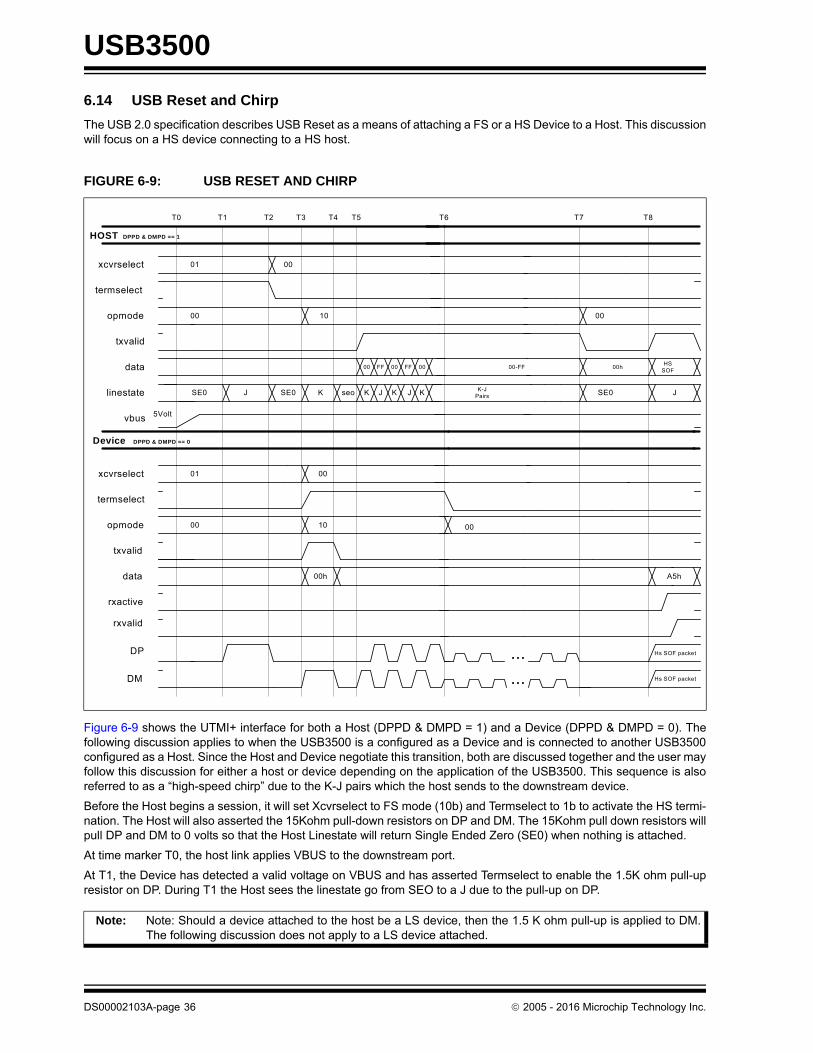
6.14 USB Reset and Chirp
The USB 2.0 specification describes USB Reset as a means of attaching a FS or a HS Device to a Host. This discussionwill focus on a HS device connecting to a HS host.
Figure 6-9 shows the UTMI+ interface for both a Host (DPPD & DMPD = 1) and a Device (DPPD & DMPD = 0). Thefollowing discussion applies to when the USB3500 is a configured as a Device and is connected to another USB3500configured as a Host. Since the Host and Device negotiate this transition, both are discussed together and the user mayfollow this discussion for either a host or device depending on the application of the USB3500. This sequence is alsoreferred to as a “high-speed chirp” due to the K-J pairs which the host sends to the downstream device.
Before the Host begins a session, it will set Xcvrselect to FS mode (10b) and Termselect to 1b to activate the HS termi-nation. The Host will also asserted the 15Kohm pull-down resistors on DP and DM. The 15Kohm pull down resistors willpull DP and DM to 0 volts so that the Host Linestate will return Single Ended Zero (SE0) when nothing is attached.
At time marker T0, the host link applies VBUS to the downstream port.
At T1, the Device has detected a valid voltage on VBUS and has asserted Termselect to enable the 1.5K ohm pull-upresistor on DP. During T1 the Host sees the linestate go from SEO to a J due to the pull-up on DP.
FIGURE 6-9: USB RESET AND CHIRP
Note: Note: Should a device attached to the host be a LS device, then the 1.5 K ohm pull-up is applied to DM.The following discussion does not apply to a LS device attached.
xcvrselect
termselect
opmode
txvalid
data
Device DPPD & DMPD == 0
HOST DPPD & DMPD == 1
vbus
xcvrselect
termselect
opmode
txvalid
linestate
data
T1T0 T2
5Volt
SE0
01
00
01 00
10
J SE0
T3 T4
00h
K seo
T5
K J K J
T6 T7 T8
K
00 FF FF00 00
rxactive
rxvalid
00 10
00
DP
DM
K-JPairs J
00
SE0
00-FFHS
SOF
A5h
00
Hs SOF packet
Hs SOF packet
00h
DS00002103A-page 36 2005 - 2016 Microchip Technology Inc.
USB3500
At T2, the Host has detected the FS device attached to the USB bus. At this time the Host will reset the bus by drivinga SE0. The SE0 is created by switching to HS Mode and activating the HS termination by de-asserting Termselect. The45 ohm high speed terminations pull the bus to SE0.
At T3, the Device will respond to the SE0 by driving a “Device Chirp K” onto the bus. The “Device Chirp K” is driven withOpmode = 10b so that bitstuffing and NRZI encoding is disabled.
During T3 the HS host will see the “Device Chirp K” and prepare to respond to the device by setting Opmode = 10b todisable the bitstuffing and NRZI encoding.
At T4, the Device will stop driving a the Chirp K, letting the bus return to SE0, and wait for the Host to respond. Thedevice removes the K by de-asserting Txvalid. The device will have driven the K for a minimum of 1mS. The Host seesthe linestate change from K to SE0.
At T5, the host begins transmitting K-J pairs to the device. Each K or J is 40-60uS long and the K-J pairs are repeatedfor the remainder of the 10mS USB reset.
At T6, the device has detected 3 K-J pairs. The device switches the Termselect low and changes Opmode to 00b. Thedevice is now in high speed and waits for the first SOF packet from the upstream host. When Termselect is de-asserted,the HS termination is activated which lowers the amplitude of the K-J pairs.
At T7, the host ends the K-J pairs and switches to normal HS mode by changing Opmode to 00b.
At T8, the Host sends the first SOF packet. This is done by putting the SOF PID 0xA5 on the data bus and assertingTxvalid. The link transfers the SOF packet. After, the SOF packet a normal high speed USB session started.
2005 - 2016 Microchip Technology Inc. DS00002103A-page 37
USB3500
6.15 Application Diagram
FIGURE 6-10: USB3500 APPLICATION DIAGRAM (TOP VIEW)
USBConnector(Standardor Mini)
UTMI+Interfaceto Link
5 VoltSupply
12K
VDD3.33.3 VoltSupply 4.
7uF
0.1u
F
1M
24M
Hz
CLOAD
ID
RB
IAS
VD
D3.
3
33
CLOAD 4.7
uF
VD
D3.
3
CVBUSHost Only
4.7
uF
0.1
uF
CVBUS
Host
Device
OTG Device
Min
100uF
1uF
1uF
Max
10uF
6.5uF
IDP
ULL
UP
XC
VR
SE
L1
LIN
ES
TA
TE
[0]
LIN
ES
TA
TE
[1]
OP
MO
DE
[1]
OP
MO
DE
[0]
CH
RG
VB
US
RX
AC
TIV
E
ID_D
IG
CLK
OU
T
VD
D1.
8
VD
D3.
3
SESSVLD
DATA[1]
DATA[0]
DATA[2]
DATA[3]
DATA[4]
DATA[5]
DATA[6]
DATA[7]
RXVALID
SESSEND
DISCHRGVBUS
HOSTDISC
VD
DA
1.8
XI
XO
VD
D1.
8
VB
US
VLD
VD
D3.
3
RX
ER
RO
R
DM
PD
DP
PD
DM
DP
VDD3.3
VDD3.3
VBUS
TXREADY
TERMSEL
XCVRSEL0
10
11
12
13
14
15 16 17 18 19 20 21 22 23 24 25 26 27 28
42
41
29
30
31
32
34
35
36
37
38
39
40
33
48 47 46 45 44 4356 55 54 53 52 51 50 49
1
2
3
4
5
6
7
8
9
USB3500Hi-Speed USBUTMI+ PHY56 Pin QFN
GND FLAG
RESET
TXVALID
SUSPENDN
ID
DM
DP
VBUS
0.1u
F
DS00002103A-page 38 2005 - 2016 Microchip Technology Inc.

USB3500
7.0 PACKAGE OUTLINE
FIGURE 7-1: USB3500-ABZJ 56-Pin QFN Package Outline, 8 x 8 x 0.9 mm Body
Not
e: F
or th
e m
ost c
urre
nt p
acka
ge d
raw
ings
, se
e th
e M
icro
chip
Pac
kagi
ng S
peci
ficat
ion
at
http
://w
ww
.mic
roch
ip.c
om/p
acka
ging
2005 - 2016 Microchip Technology Inc. DS00002103A-page 39
USB3500
FIGURE 7-1: USB3500-ABZJ 56-Pin QFN Package Outline, 8 x 8 x 0.9 mm Body (continued)
Not
e: F
or th
e m
ost c
urre
nt p
acka
ge d
raw
ings
, se
e th
e M
icro
chip
Pac
kagi
ng S
peci
ficat
ion
at
http
://w
ww
.mic
roch
ip.c
om/p
acka
ging
DS00002103A-page 40 2005 - 2016 Microchip Technology Inc.

2005 - 2016 Microchip Technology Inc. DS00002103A-page 41
USB3500
APPENDIX A: REVISION HISTORY
TABLE A-1: REVISION HISTORY
Revision Section/Figure/Entry Correction
DS00002103A (02-10-16) Replaces previous SMSC version Rev. 1.0 (06-05-08)
USB3500
DS00002103A-page 42 2005 - 2016 Microchip Technology Inc.
THE MICROCHIP WEB SITE
Microchip provides online support via our WWW site at www.microchip.com. This web site is used as a means to makefiles and information easily available to customers. Accessible by using your favorite Internet browser, the web site con-tains the following information:
• Product Support – Data sheets and errata, application notes and sample programs, design resources, user’s guides and hardware support documents, latest software releases and archived software
• General Technical Support – Frequently Asked Questions (FAQ), technical support requests, online discussion groups, Microchip consultant program member listing
• Business of Microchip – Product selector and ordering guides, latest Microchip press releases, listing of semi-nars and events, listings of Microchip sales offices, distributors and factory representatives
CUSTOMER CHANGE NOTIFICATION SERVICE
Microchip’s customer notification service helps keep customers current on Microchip products. Subscribers will receivee-mail notification whenever there are changes, updates, revisions or errata related to a specified product family ordevelopment tool of interest.
To register, access the Microchip web site at www.microchip.com. Under “Support”, click on “Customer Change Notifi-cation” and follow the registration instructions.
CUSTOMER SUPPORT
Users of Microchip products can receive assistance through several channels:
• Distributor or Representative
• Local Sales Office
• Field Application Engineer (FAE)
• Technical Support
Customers should contact their distributor, representative or field application engineer (FAE) for support. Local salesoffices are also available to help customers. A listing of sales offices and locations is included in the back of this docu-ment.
Technical support is available through the web site at: http://www.microchip.com/support
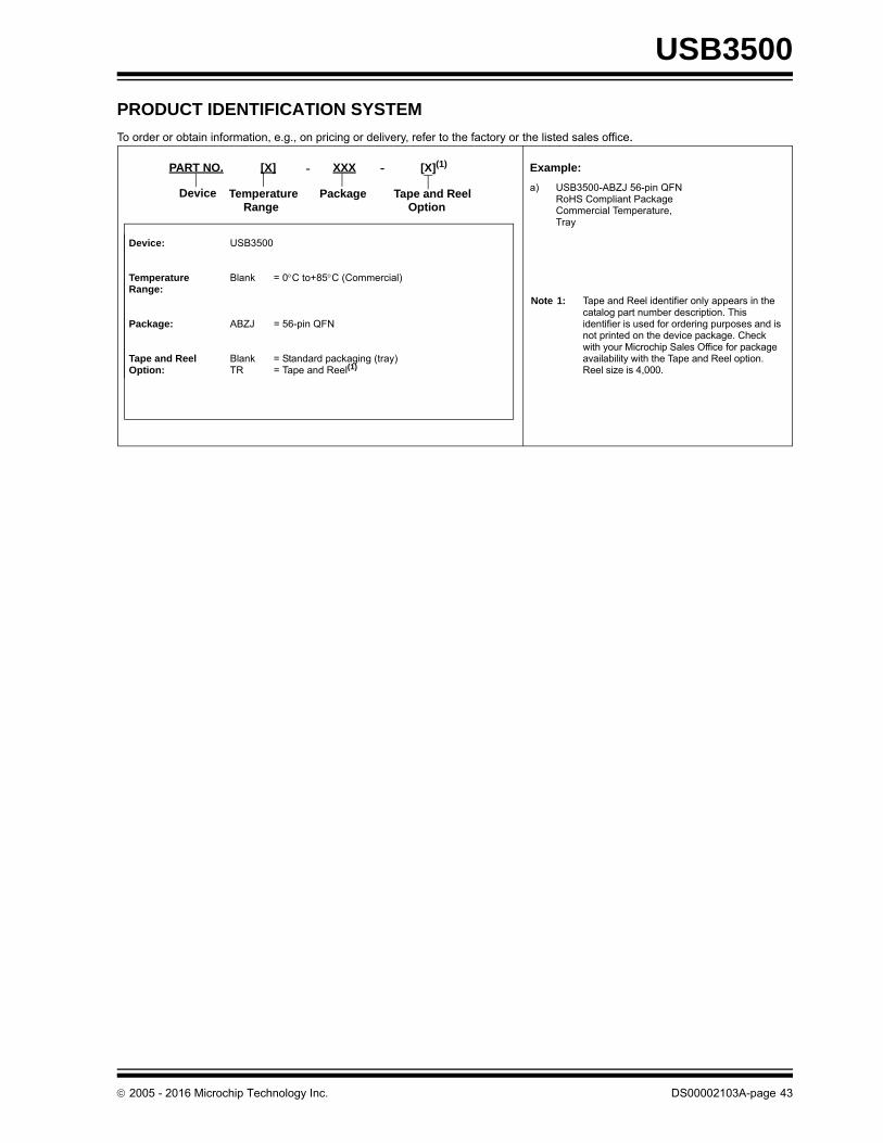
2005 - 2016 Microchip Technology Inc. DS00002103A-page 43
USB3500
PRODUCT IDENTIFICATION SYSTEM
To order or obtain information, e.g., on pricing or delivery, refer to the factory or the listed sales office.
Device: USB3500
Temperature Range:
Blank = 0C to+85C (Commercial)
Package: ABZJ = 56-pin QFN
Tape and Reel Option:
Blank = Standard packaging (tray)TR = Tape and Reel(1)
Example:
a) USB3500-ABZJ 56-pin QFN RoHS Compliant PackageCommercial Temperature,Tray
Note 1: Tape and Reel identifier only appears in the catalog part number description. This identifier is used for ordering purposes and is not printed on the device package. Check with your Microchip Sales Office for package availability with the Tape and Reel option.Reel size is 4,000.
PART NO. [X] XXX
PackageTemperatureRange
Device
[X](1)
Tape and ReelOption
- -
USB3500
DS00002103A-page 44 2005 - 2016 Microchip Technology Inc.
Information contained in this publication regarding device applications and the like is provided only for your convenience and may be super-seded by updates. It is your responsibility to ensure that your application meets with your specifications. MICROCHIP MAKES NO REP-RESENTATIONS OR WARRANTIES OF ANY KIND WHETHER EXPRESS OR IMPLIED, WRITTEN OR ORAL, STATUTORY OROTHERWISE, RELATED TO THE INFORMATION, INCLUDING BUT NOT LIMITED TO ITS CONDITION, QUALITY, PERFORMANCE,MERCHANTABILITY OR FITNESS FOR PURPOSE. Microchip disclaims all liability arising from this information and its use. Use of Micro-chip devices in life support and/or safety applications is entirely at the buyer’s risk, and the buyer agrees to defend, indemnify and holdharmless Microchip from any and all damages, claims, suits, or expenses resulting from such use. No licenses are conveyed, implicitly orotherwise, under any Microchip intellectual property rights unless otherwise stated.
Trademarks
The Microchip name and logo, the Microchip logo, dsPIC, FlashFlex, flexPWR, JukeBlox, KEELOQ, KEELOQ logo, Kleer, LANCheck, MediaLB, MOST, MOST logo, MPLAB, OptoLyzer, PIC, PICSTART, PIC32 logo, RightTouch, SpyNIC, SST, SST Logo, SuperFlash and UNI/O are registered trademarks of Microchip Technology Incorporated in the U.S.A. and other countries.
The Embedded Control Solutions Company and mTouch are registered trademarks of Microchip Technology Incorporated in the U.S.A.
Analog-for-the-Digital Age, BodyCom, chipKIT, chipKIT logo, CodeGuard, dsPICDEM, dsPICDEM.net, ECAN, In-Circuit Serial Programming, ICSP, Inter-Chip Connectivity, KleerNet, KleerNet logo, MiWi, motorBench, MPASM, MPF, MPLAB Certified logo, MPLIB, MPLINK, MultiTRAK, NetDetach, Omniscient Code Generation, PICDEM, PICDEM.net, PICkit, PICtail, RightTouch logo, REAL ICE, SQI, Serial Quad I/O, Total Endurance, TSHARC, USBCheck, VariSense, ViewSpan, WiperLock, Wireless DNA, and ZENA are trademarks of Microchip Technology Incorporated in the U.S.A. and other countries.
SQTP is a service mark of Microchip Technology Incorporated in the U.S.A.
Silicon Storage Technology is a registered trademark of Microchip Technology Inc. in other countries.
GestIC is a registered trademark of Microchip Technology Germany II GmbH & Co. KG, a subsidiary of Microchip Technology Inc., in other countries.
All other trademarks mentioned herein are property of their respective companies.
© 2005 - 2016, Microchip Technology Incorporated, Printed in the U.S.A., All Rights Reserved.
ISBN: 9781522402800
Note the following details of the code protection feature on Microchip devices:
• Microchip products meet the specification contained in their particular Microchip Data Sheet.
• Microchip believes that its family of products is one of the most secure families of its kind on the market today, when used in the intended manner and under normal conditions.
• There are dishonest and possibly illegal methods used to breach the code protection feature. All of these methods, to our knowledge, require using the Microchip products in a manner outside the operating specifications contained in Microchip’s Data Sheets. Most likely, the person doing so is engaged in theft of intellectual property.
• Microchip is willing to work with the customer who is concerned about the integrity of their code.
• Neither Microchip nor any other semiconductor manufacturer can guarantee the security of their code. Code protection does not mean that we are guaranteeing the product as “unbreakable.”
Code protection is constantly evolving. We at Microchip are committed to continuously improving the code protection features of ourproducts. Attempts to break Microchip’s code protection feature may be a violation of the Digital Millennium Copyright Act. If such actsallow unauthorized access to your software or other copyrighted work, you may have a right to sue for relief under that Act.
Microchip received ISO/TS-16949:2009 certification for its worldwide headquarters, design and wafer fabrication facilities in Chandler and Tempe, Arizona; Gresham, Oregon and design centers in California and India. The Company’s quality system processes and procedures are for its PIC® MCUs and dsPIC® DSCs, KEELOQ® code hopping devices, Serial EEPROMs, microperipherals, nonvolatile memory and analog products. In addition, Microchip’s quality system for the design and manufacture of development systems is ISO 9001:2000 certified.
QUALITYMANAGEMENTSYSTEMCERTIFIEDBYDNV
== ISO/TS16949==

2005 - 2016 Microchip Technology Inc. DS00002103A-page 45
AMERICASCorporate Office2355 West Chandler Blvd.Chandler, AZ 85224-6199Tel: 480-792-7200 Fax: 480-792-7277Technical Support: http://www.microchip.com/supportWeb Address: www.microchip.com
AtlantaDuluth, GA Tel: 678-957-9614 Fax: 678-957-1455
Austin, TXTel: 512-257-3370
BostonWestborough, MA Tel: 774-760-0087 Fax: 774-760-0088
ChicagoItasca, IL Tel: 630-285-0071 Fax: 630-285-0075
ClevelandIndependence, OH Tel: 216-447-0464 Fax: 216-447-0643
DallasAddison, TX Tel: 972-818-7423 Fax: 972-818-2924
DetroitNovi, MI Tel: 248-848-4000
Houston, TX Tel: 281-894-5983
IndianapolisNoblesville, IN Tel: 317-773-8323Fax: 317-773-5453
Los AngelesMission Viejo, CA Tel: 949-462-9523 Fax: 949-462-9608
New York, NY Tel: 631-435-6000
San Jose, CA Tel: 408-735-9110
Canada - TorontoTel: 905-673-0699 Fax: 905-673-6509
ASIA/PACIFICAsia Pacific OfficeSuites 3707-14, 37th FloorTower 6, The GatewayHarbour City, Kowloon
Hong KongTel: 852-2943-5100Fax: 852-2401-3431
Australia - SydneyTel: 61-2-9868-6733Fax: 61-2-9868-6755
China - BeijingTel: 86-10-8569-7000 Fax: 86-10-8528-2104
China - ChengduTel: 86-28-8665-5511Fax: 86-28-8665-7889
China - ChongqingTel: 86-23-8980-9588Fax: 86-23-8980-9500
China - DongguanTel: 86-769-8702-9880
China - HangzhouTel: 86-571-8792-8115 Fax: 86-571-8792-8116
China - Hong Kong SARTel: 852-2943-5100 Fax: 852-2401-3431
China - NanjingTel: 86-25-8473-2460Fax: 86-25-8473-2470
China - QingdaoTel: 86-532-8502-7355Fax: 86-532-8502-7205
China - ShanghaiTel: 86-21-5407-5533 Fax: 86-21-5407-5066
China - ShenyangTel: 86-24-2334-2829Fax: 86-24-2334-2393
China - ShenzhenTel: 86-755-8864-2200 Fax: 86-755-8203-1760
China - WuhanTel: 86-27-5980-5300Fax: 86-27-5980-5118
China - XianTel: 86-29-8833-7252Fax: 86-29-8833-7256
ASIA/PACIFICChina - XiamenTel: 86-592-2388138 Fax: 86-592-2388130
China - ZhuhaiTel: 86-756-3210040 Fax: 86-756-3210049
India - BangaloreTel: 91-80-3090-4444 Fax: 91-80-3090-4123
India - New DelhiTel: 91-11-4160-8631Fax: 91-11-4160-8632
India - PuneTel: 91-20-3019-1500
Japan - OsakaTel: 81-6-6152-7160 Fax: 81-6-6152-9310
Japan - TokyoTel: 81-3-6880- 3770 Fax: 81-3-6880-3771
Korea - DaeguTel: 82-53-744-4301Fax: 82-53-744-4302
Korea - SeoulTel: 82-2-554-7200Fax: 82-2-558-5932 or 82-2-558-5934
Malaysia - Kuala LumpurTel: 60-3-6201-9857Fax: 60-3-6201-9859
Malaysia - PenangTel: 60-4-227-8870Fax: 60-4-227-4068
Philippines - ManilaTel: 63-2-634-9065Fax: 63-2-634-9069
SingaporeTel: 65-6334-8870Fax: 65-6334-8850
Taiwan - Hsin ChuTel: 886-3-5778-366Fax: 886-3-5770-955
Taiwan - KaohsiungTel: 886-7-213-7828
Taiwan - TaipeiTel: 886-2-2508-8600 Fax: 886-2-2508-0102
Thailand - BangkokTel: 66-2-694-1351Fax: 66-2-694-1350
EUROPEAustria - WelsTel: 43-7242-2244-39Fax: 43-7242-2244-393
Denmark - CopenhagenTel: 45-4450-2828 Fax: 45-4485-2829
France - ParisTel: 33-1-69-53-63-20 Fax: 33-1-69-30-90-79
Germany - DusseldorfTel: 49-2129-3766400
Germany - KarlsruheTel: 49-721-625370
Germany - MunichTel: 49-89-627-144-0 Fax: 49-89-627-144-44
Italy - Milan Tel: 39-0331-742611 Fax: 39-0331-466781
Italy - VeniceTel: 39-049-7625286
Netherlands - DrunenTel: 31-416-690399 Fax: 31-416-690340
Poland - WarsawTel: 48-22-3325737
Spain - MadridTel: 34-91-708-08-90Fax: 34-91-708-08-91
Sweden - StockholmTel: 46-8-5090-4654
UK - WokinghamTel: 44-118-921-5800Fax: 44-118-921-5820
Worldwide Sales and Service
07/14/15