Embed Size (px)
Citation preview

Micro-RDCMicroelectronics Research Development Corporation
Use of FPGAs For Radiation Testing
MAFANovember 28, 2007
Paul EatonMicro-RDC
8102 Menaul Blvd. NE, Suites C&DAlbuquerque, NM 87110
505-294-1962
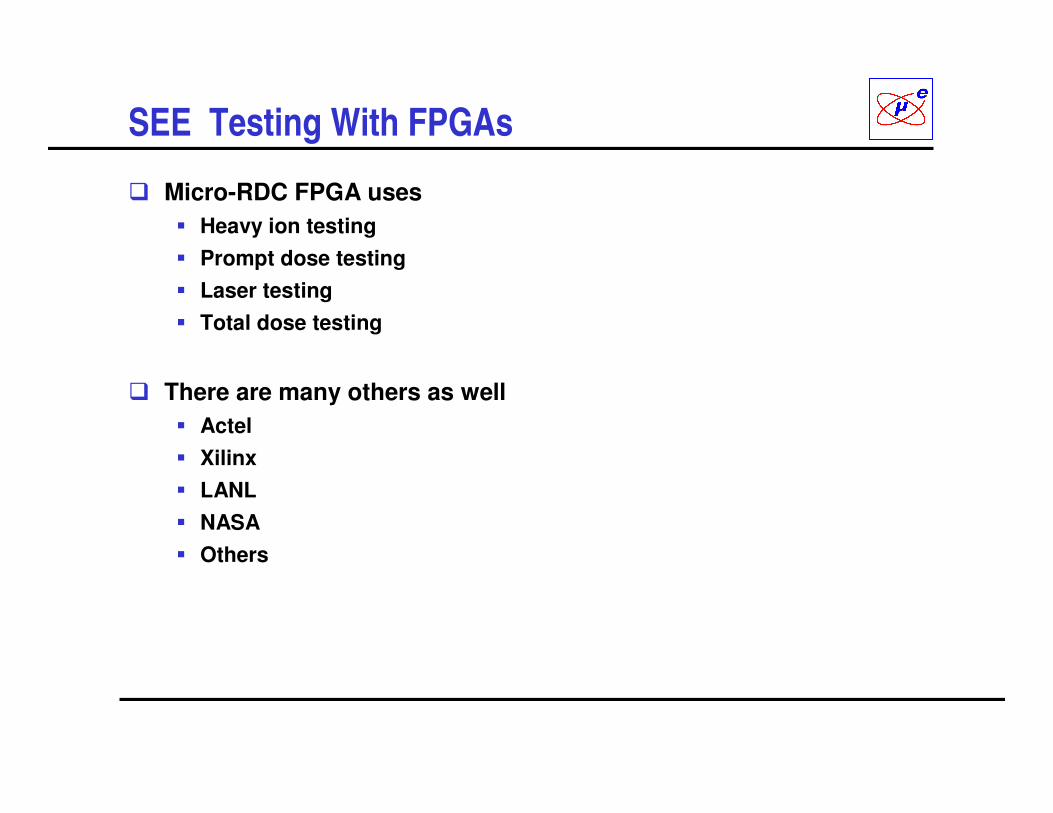
SEE Testing With FPGAs
� Micro-RDC FPGA uses� Heavy ion testing� Prompt dose testing� Laser testing� Total dose testing
� There are many others as well� Actel� Xilinx� LANL� NASA� Others

Original ECL Digital Single Event Transient Board
� Early ECL board design� Specific design to each test chip� High-speed test clock,
low-speed interface clock• Experiment relied on the error-
detection circuitry built into the test chip
� New board was required for each new test chip design
• Time consuming and costly

FPGA Test System Concepts
� Speed� Move the test system (FPGA) as close to the device
under test (DUT) as possible
� Cost� Make the board as flexible as possible, minimize the
re-design necessary for a variety of DUTs
� Re-Use� VHDL code� Coding style for portability
• Build using most generic constructs– Some modules still used on the Virtex-5 board were
first built on the Virtex-2 board
• Isolate special FPGA component usage into separate modules
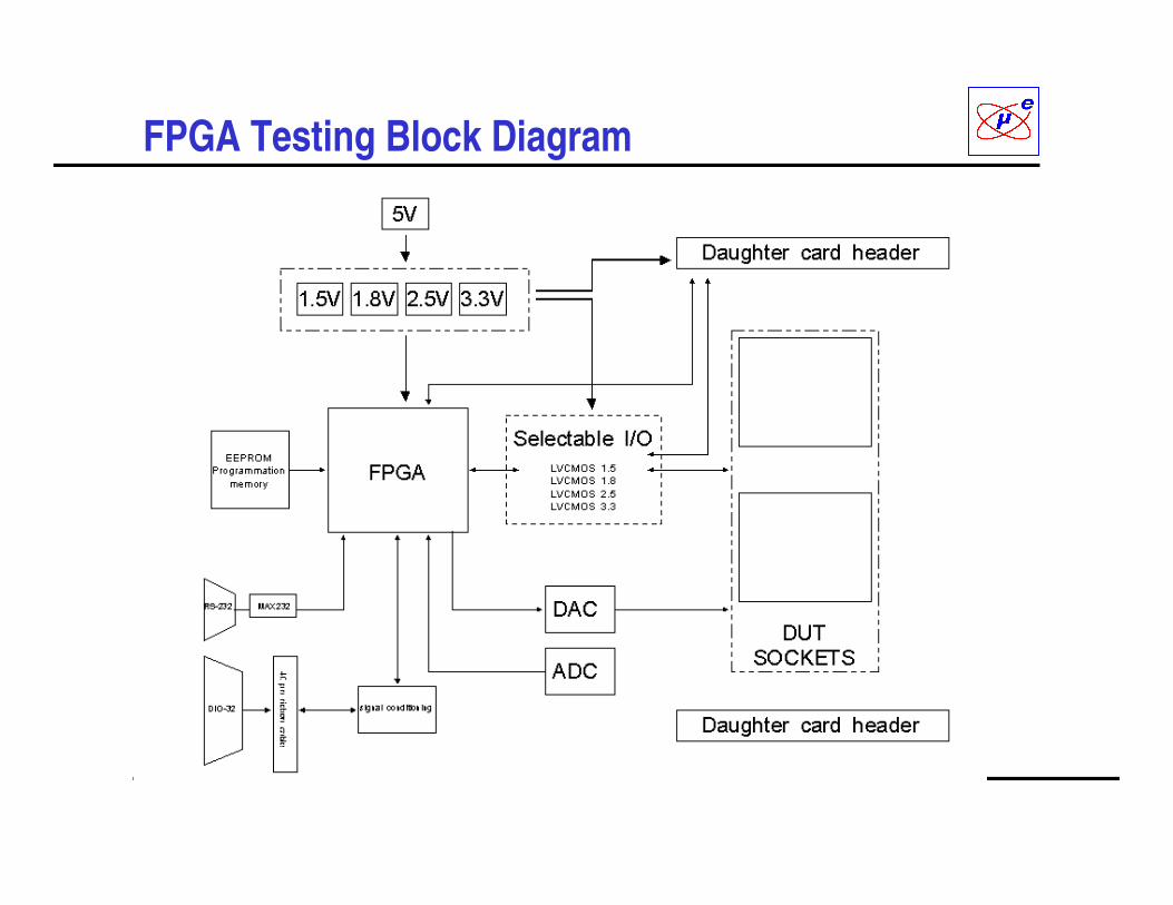
FPGA Testing Block Diagram

Virtex 2 DSET Board
� Upgrade from ECL board� RS232 interface� National Instruments DIO-32
connector� Adjustable voltage interface to
the FPGA pins� “Generic” socket definition
• Pwr/Gnd had to be defined• 84-pin LCC socket
� Daughter card connectors• Daughter card mounts over the
sockets• Daughter card with ribbon cables
used for experiments requiring the FPGA to be shielded

Spartan-3 DSET Board �System designed around XilinxSpartan-3 FPGA�Maintains compatibility with previous Virtex-2 DSET system� Pinout from 84-pin LCC socket
maintained�Use of new low-impedance interconnect technology for high speed testing
�New higher speed daughter card connections� Daughter card connections based
on NASA Spartan-3 board design
�Main upgrades� Faster test capability� Lower VDD on I/Os to test device

New Virtex-5 DSET Board
� Upgrade from Spartan-3 to V5� Higher logic density
• Xilinx recommends 64-bit Linux PC with 2 GB of RAM
� More I/O (560 user I/O)• Completely separate I/O to particle
interconnect and daughtercard
� New board components� Level shifting transceivers for
under 1.0V I/O requirements� USB interface module
• Faster communication/data transfer rates
� Programmable clock IC• Up to 700 MHz

Spartan-3 4-LUT
� 4-Input Look-up tables

Virtex-5 6-LUT
� 6-Input look-up tables

(Pre)-Test Checklist
� Find out all information possible before the experiment� What new software needs to be designed� Physical facility information
• Cabling• Bulkhead feed-throughs• Electrical noise• Distance from chamber
� How to log the expected results from DUT� Latchup� SEUs� Loss of functionality
� What to do when the part reacts unexpectedly to the radiation source� Reset part and record event� Cycle power and record event

General Experiment Design & Test Concepts
� Board and DUT power� How far away will the power supplies be from the DUT� How will the power supplies be monitored
� Communication interface � How fast does the interface need to be� How much noise will be acceptable on the communication interface
� Part exposure� How will the test board be mounted� How will the DUT be mounted
• Will the die require thinning• Will high angle testing be performed
– How high an angle can be reached
� FPGA protection� Will the FPGA receive any undesired exposure� Will the FPGA need shielding� Can the FPGA be powered down during the test

VHDL Block Level Design
� State machine design� Generic VHDL� Isolate specialized
blocks (DCM, block RAM)
• Easier to port to new designs
� Perl scripts generate VHDL for Receive (RX) & Transmit (TX) blocks
� Main state machine� New code specific to
the DUT

Perl VHDL Generation
� Example input to RX generator
L%Toggle_LED %Toggle %C0%N0% test HWD%CDC_ICS_clock_divider %Pulse %C4%N1% selects the muxE%CDC_force_data_error %Clear %C0%N0% V%PDTRL_Verbosity %Pulse %C4%N1% Verbosity setting

Example: SRAM SEU Testing
� Multiple test modes� Bench test
• Make sure the part is correct before the test• Commercial marching/galloping patterns
� Static test for heavy ion testing• Load known pattern• Expose DUT to heavy ions• Read back the data, scan for changes
� Dynamic test• Read/Write• Read only = Primary test mode

Example: Multi-Bit Upset Data Acquisition
� Measurement procedure� Write SRAM with bit pattern to ensure groupings of NMOS and
PMOS reverse biased junctions� Read entire SRAM with EDAC disabled, and correct any errors� Repeat process every 5 to 6 ms
� For each error� Log the expected and received data bits in the word� Log the word address of the error� Log the time stamp (simply the loop counter)
� Sample log file

MBU Data Analysis
� Parse each error in log file to display layout location� XOR expected and received to identify physical 8k block of memory� From data state before error, identify reverse biased junctions within
the bit cell� From address, simply use LVS mapping to highlight nodes in the
layout corresponding to these bit cell junctions
� Parse log file to identify and categorize MBUs� XOR expected and received to identify physical 8k block of memory� From address, compute row and column location of upset bit� From data state before error, identify quadrants of bit cell containing
reverse biased junctions� For errors within same time stamp, locate adjacent bit cells with
adjacent reverse biased junctions� Determine MBU type (multiple NMOS strike, multiple PMOS strike)� Determine MBU multiplicity (double, triple, quadruple)

SRAM SEU Errors
� Use LVS mapping to plot reverse biased junctions of each bit error� Dave Mavis and Mike Sibley designed Perl script to extract all cross-sections
from the raw data (single PMOS hit, NMOS hit, multiple PMOS/NMOS)
90 nm Bulk CMOS SRAM
Vdd = 1.2 V
LET = 59.1 MeV-cm2/mg
Probability of any given MBUarising from multiple particlesin same 5.6 ms time stamp:2-particle MBU : 1.9 x 10-63-particle MBU : 3.6 x 10-124-particle MBU : 6.8 x 10⁻¹⁸

Extraction of Each Type of MBU
� Error cross section dominated by MBUs above 20 MeV-cm2/mg� Single bit errors account for only 16% of the total errors� Double, triple, quadruple PMOS most prevalent� Double, triple, quadruple NMOS less important

Data Analysis
� Curve fitting code� Dave Mavis integrated multiple waveform types into curve fit code libraries
� Example: 90nm SRAM designed by Micro-RDC� Data represents the measured total error cross section� Weibull fit can be done, but again with unphysical parameters� Lognormal is now from a fit to extracted single bit errors� Cross section jump suggests high multiplicity MBUs

In Summary
� Get as much information on the part as possible� All functional testing
� Determine most appropriate die package� PGA� Chip-on-board
� Build test code� Re-use as much as possible
� Data analysis� Work on test analysis framework before the test
• Help determine what data must be recorded
� Run experiment
* Special thanks to DTRA for funding much of the test system development on the DSET programs