Embed Size (px)
Citation preview
FC5A SERIES
FC9Y-B1273(2)
User’s Manual Advanced Volume


SAFETY PRECAUTIONS
•Read this user’s manual to make sure of correct operation before starting installation, wiring, operation, maintenance, and inspection of the MicroSmart.
•All MicroSmart modules are manufactured under IDEC’s rigorous quality control system, but users must add a backup or failsafe provision to the control system when using the MicroSmart in applications where heavy damage or personal injury may be caused in case the MicroSmart should fail.
•In this user’s manual, safety precautions are categorized in order of importance to Warning and Caution:
•Turn off power to the MicroSmart before installation, removal, wiring, maintenance, and inspection of the MicroSmart. Failure to turn power off may cause electrical shocks or fire hazard.
•Special expertise is required to install, wire, program, and operate the MicroSmart. People without such expertise must not use the MicroSmart.
•Emergency stop and interlocking circuits must be configured outside the MicroSmart. If such a circuit is configured inside the MicroSmart, failure of the MicroSmart may cause disorder of the control system, damage, or accidents.
•Install the MicroSmart according to the instructions described in this user’s manual. Improper installation will result in falling, failure, or malfunction of the MicroSmart.
•The MicroSmart is designed for installation in a cabinet. Do not install the MicroSmart outside a cabinet.
•Install the MicroSmart in environments described in this user’s manual. If the MicroSmart is used in places where the MicroSmart is subjected to high‐temperature, high‐humidity, condensation, corrosive gases, excessive vibrations, and excessive shocks, then electrical shocks, fire hazard, or malfunction will result.
•The environment for using the MicroSmart is “Pollution degree 2.” Use the MicroSmart in environments of pollution degree 2 (according to IEC 60664‐1).
•Prevent the MicroSmart from falling while moving or transporting the MicroSmart, otherwise damage or malfunction of the MicroSmart will result.
•Prevent metal fragments and pieces of wire from dropping inside the MicroSmart housing. Put a cover on the MicroSmart modules during installation and wiring. Ingress of such fragments and chips may cause fire hazard, damage, or malfunc‐tion.
•Use a power supply of the rated value. Use of a wrong power supply may cause fire hazard.
•Use an IEC 60127‐approved fuse on the power line outside the MicroSmart. This is required when equipment containing the MicroSmart is destined for Europe.
•Use an IEC 60127‐approved fuse on the output circuit. This is required when equipment containing the MicroSmart is des‐tined for Europe.
•Use an EU‐approved circuit breaker. This is required when equipment containing the MicroSmart is destined for Europe.
•Make sure of safety before starting and stopping the MicroSmart or when operating the MicroSmart to force outputs on or off. Incorrect operation on the MicroSmart may cause machine damage or accidents.
•If relays or transistors in the MicroSmart output modules should fail, outputs may remain on or off. For output signals which may cause heavy accidents, provide a monitor circuit outside the MicroSmart.
•Do not connect the ground wire directly to the MicroSmart. Connect a protective ground to the cabinet containing the MicroSmart using an M4 or larger screw. This is required when equipment containing the MicroSmart is destined for Europe.
•Do not disassemble, repair, or modify the MicroSmart modules.
•Dispose of the battery in the MicroSmart modules when the battery is dead in accordance with pertaining regulations. When storing or disposing of the battery, use a proper container prepared for this purpose. This is required when equip‐ment containing the MicroSmart is destined for Europe.
•When disposing of the MicroSmart, do so as an industrial waste.
Warning Warning notices are used to emphasize that improper operation may cause severe personal injury or death.
Caution Caution notices are used where inattention might cause personal injury or dam‐age to equipment.
FC5A MicroSmart User’s Manual FC9Y‐B1273 Preface‐1
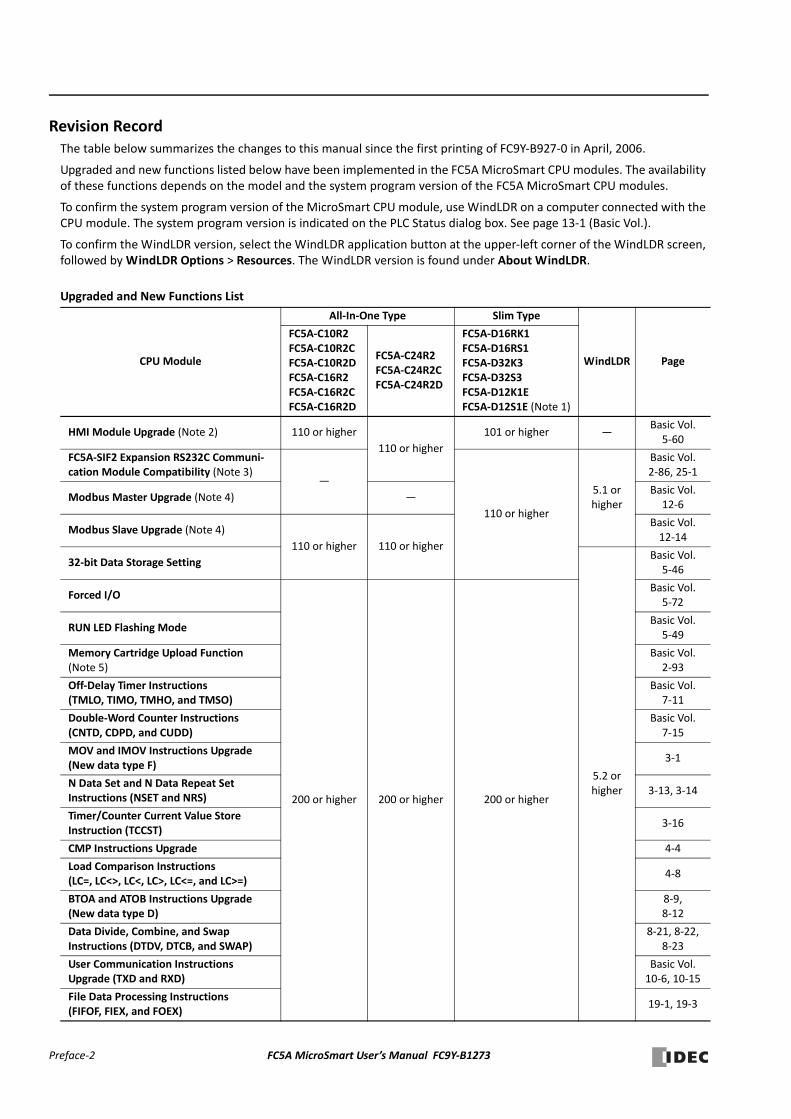
Revision RecordThe table below summarizes the changes to this manual since the first printing of FC9Y‐B927‐0 in April, 2006.
Upgraded and new functions listed below have been implemented in the FC5A MicroSmart CPU modules. The availability of these functions depends on the model and the system program version of the FC5A MicroSmart CPU modules.
To confirm the system program version of the MicroSmart CPU module, use WindLDR on a computer connected with the CPU module. The system program version is indicated on the PLC Status dialog box. See page 13‐1 (Basic Vol.).
To confirm the WindLDR version, select the WindLDR application button at the upper‐left corner of the WindLDR screen, followed by WindLDR Options > Resources. The WindLDR version is found under About WindLDR.
Upgraded and New Functions List
CPU Module
All‐In‐One Type Slim Type
WindLDR Page
FC5A‐C10R2FC5A‐C10R2CFC5A‐C10R2DFC5A‐C16R2FC5A‐C16R2CFC5A‐C16R2D
FC5A‐C24R2FC5A‐C24R2CFC5A‐C24R2D
FC5A‐D16RK1FC5A‐D16RS1FC5A‐D32K3FC5A‐D32S3FC5A‐D12K1EFC5A‐D12S1E (Note 1)
HMI Module Upgrade (Note 2) 110 or higher
110 or higher
101 or higher —Basic Vol. 5‐60
FC5A‐SIF2 Expansion RS232C Communi‐cation Module Compatibility (Note 3)
—
110 or higher
5.1 or higher
Basic Vol. 2‐86, 25‐1
Modbus Master Upgrade (Note 4) —Basic Vol. 12‐6
Modbus Slave Upgrade (Note 4)
110 or higher 110 or higher
Basic Vol. 12‐14
32‐bit Data Storage Setting
5.2 or higher
Basic Vol. 5‐46
Forced I/O
200 or higher 200 or higher 200 or higher
Basic Vol. 5‐72
RUN LED Flashing ModeBasic Vol. 5‐49
Memory Cartridge Upload Function(Note 5)
Basic Vol. 2‐93
Off‐Delay Timer Instructions (TMLO, TIMO, TMHO, and TMSO)
Basic Vol. 7‐11
Double‐Word Counter Instructions (CNTD, CDPD, and CUDD)
Basic Vol. 7‐15
MOV and IMOV Instructions Upgrade(New data type F)
3‐1
N Data Set and N Data Repeat Set Instructions (NSET and NRS)
3‐13, 3‐14
Timer/Counter Current Value Store Instruction (TCCST)
3‐16
CMP Instructions Upgrade 4‐4
Load Comparison Instructions(LC=, LC<>, LC<, LC>, LC<=, and LC>=)
4‐8
BTOA and ATOB Instructions Upgrade(New data type D)
8‐9, 8‐12
Data Divide, Combine, and Swap Instructions (DTDV, DTCB, and SWAP)
8‐21, 8‐22, 8‐23
User Communication Instructions Upgrade (TXD and RXD)
Basic Vol. 10‐6, 10‐15
File Data Processing Instructions (FIFOF, FIEX, and FOEX)
19‐1, 19‐3
Preface‐2 FC5A MicroSmart User’s Manual FC9Y‐B1273
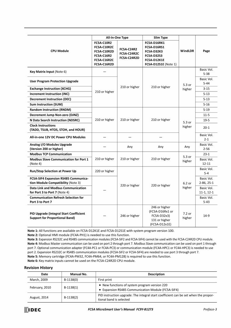
Note 1: All functions are available on FC5A‐D12K1E and FC5A‐D12S1E with system program version 100.Note 2: Optional HMI module (FC4A‐PH1) is needed to use this function.Note 3: Expansion RS232C and RS485 communication modules (FC5A‐SIF2 and FC5A‐SIF4) cannot be used with the FC5A‐C24R2D CPU module.Note 4: Modbus Master communication can be used on port 2 through port 7. Modbus Slave communication can be used on port 1 through port 7. Optional communication adapter (FC4A‐PC1 or FC4A‐PC3) or communication module (FC4A‐HPC1 or FC4A‐HPC3) is needed to use port 2. Expansion RS232C or RS485 communication modules (FC5A‐SIF2 or FC5A‐SIF4) are needed to use port 3 through port 7.Note 5: Memory cartridge (FC4A‐PM32, FC4A‐PM64, or FC4A‐PM128) is required to use this function.Note 6: Key matrix inputs cannot be used on the FC5A‐C24R2D CPU module.
Revision History
Key Matrix Input (Note 6) —
210 or higher 210 or higher5.3 or higher
Basic Vol. 5‐38
User Program Protection Upgrade
210 or higher
Basic Vol. 5‐44
Exchange Instruction (XCHG) 3‐15
Increment Instruction (INC) 5‐13
Decrement Instruction (DEC) 5‐13
Sum Instruction (SUM) 5‐16
Random Instruction (RNDM)
210 or higher 210 or higher 210 or higher5.3 or higher
5‐19
Decrement Jump Non‐zero (DJNZ) 11‐5
N Data Search Instruction (NDSRC) 19‐5
Clock Instructions (TADD, TSUB, HTOS, STOH, and HOUR)
20‐1
All‐in‐one 12V DC Power CPU Modules — — —Basic Vol.
2‐1
Analog I/O Modules Upgrade(Version 200 or higher)
— Any Any AnyBasic Vol. 2‐56
Modbus TCP Communication
210 or higher 210 or higher 210 or higher5.3 or higher
23‐1
Modbus Slave Communication for Port 1 (Note 4)
Basic Vol. 12‐11
Run/Stop Selection at Power Up 220 or higher
220 or higher 220 or higher6.2 or higher
Basic Vol. 5‐4
FC5A‐SIF4 Expansion RS485 Communica‐tion Module Compatibility (Note 3)
—
Basic Vol. 2‐86, 25‐1
Data Link and Modbus Communication for Port 3 to Port 7 (Note 4)
Basic Vol. 11‐1, 12‐1
Communication Refresh Selection for Port 3 to Port 7
Basic Vol. 5‐43
PID Upgrade (Integral Start Coefficient Support for Proportional Band)
— 246 or higher
246 or higher (FC5A‐D16Rx1 or FC5A‐D32x3)131 or higher (FC5A‐D12x1E)
7.2 or higher
14‐9
Date Manual No. Description
March, 2009 B‐1138(0) First print
February, 2010 B‐1138(1) New functions of system program version 220
Expansion RS485 Communication Module (FC5A‐SIF4)
August, 2014 B‐1138(2)PID instruction upgrade: The integral start coefficient can be set when the propor‐tional band is selected
CPU Module
All‐In‐One Type Slim Type
WindLDR Page
FC5A‐C10R2FC5A‐C10R2CFC5A‐C10R2DFC5A‐C16R2FC5A‐C16R2CFC5A‐C16R2D
FC5A‐C24R2FC5A‐C24R2CFC5A‐C24R2D
FC5A‐D16RK1FC5A‐D16RS1FC5A‐D32K3FC5A‐D32S3FC5A‐D12K1EFC5A‐D12S1E (Note 1)
FC5A MicroSmart User’s Manual FC9Y‐B1273 Preface‐3

About This Manual
This user’s manual primarily describes programming and powerful communications of the MicroSmart.
Chapter 1: Basic Instructions ReferenceProgramming of the basic instructions, available devices, and sample programs.
Chapter 2: Advanced InstructionsGeneral rules of using advanced instructions, terms, data types, and formats used for advanced instructions.
Chapter 3 through Chapter 20:Detailed descriptions on advanced instructions grouped into 18 chapters.
Chapter 21 through Chapter 25:Various communication functions such as computer link, modem mode, Modbus TCP, AS‐Interface, and expansion RS232C/RS485 communication.
IndexAlphabetical listing of key words.
IMPORTANT INFORMATION
Under no circumstances shall IDEC Corporation be held liable or responsible for indirect or consequential damages resulting from the use of or the application of IDEC PLC components, individually or in combination with other equipment.
All persons using these components must be willing to accept responsibility for choosing the correct component to suit their application and for choosing an application appropriate for the component, individually or in combination with other equipment.
All diagrams and examples in this manual are for illustrative purposes only. In no way does including these diagrams and examples in this manual constitute a guarantee as to their suitability for any specific application. To test and approve all programs, prior to installation, is the responsibility of the end user.
Preface‐4 FC5A MicroSmart User’s Manual FC9Y‐B1273

RELATED MANUALS
The following manuals related to the FC5A series MicroSmart are available. Refer to them in conjunction with this man‐ual.
Type No. Manual Name Description
FC9Y‐B1273
FC5A SeriesMicroSmart PentraUser's ManualAdvanced Volume (this manual)
Describes basic instruction list, move instructions, data comparison instruc‐tions, binary arithmetic instructions, boolean computation instructions, shift/rotate instructions, data conversion instructions, week programmer instructions, interface instructions, program branching instructions, refresh instructions, interrupt control instructions, coordinate conversion instruc‐tions, average instructions, pulse output instructions, PID instructions, dual/teaching timer instructions, intelligent module access instructions, trigono‐metric function instructions, logarithm/power instructions, file data process‐ing instructions, clock instructions, computer link communication, modem communication, Modbus TCP communication, expansion RS232C/RS485 communication modules, and AS‐Interface master modules.
FC9Y‐B1268
FC5A SeriesMicroSmart PentraUser's ManualBasic Volume
Describes module specifications, installation instructions, wiring instructions, basic operation, function settings, device list, basic instruction list, basic instructions, analog modules, user communication, data link communication, Modbus ASCII/RTU communication, and troubleshooting.
FC9Y‐B1278
FC5A SeriesMicroSmart PentraUser's ManualWeb Server CPU Module Volume
Describes FC5A Slim Type Web Server CPU Module specifications and func‐tions.
FC9Y‐B1283FC5A SeriesPID ModuleUser's Manual
Describes PID Module specifications and functions.
FC5A MicroSmart User’s Manual FC9Y‐B1273 Preface‐5

Preface‐6 FC5A MicroSmart User’s Manual FC9Y‐B1273
TABLE OF CONTENTS
CHAPTER 1: Basic Instructions ReferenceBasic Instruction List . . . . . . . . . . . . . . . . . . . . . . . . . . . . . . . . . . . . . . . . . . . . . . . . . . . . . . . . . . . . . . . . . 1‐1
CHAPTER 2: Advanced InstructionsAdvanced Instruction List . . . . . . . . . . . . . . . . . . . . . . . . . . . . . . . . . . . . . . . . . . . . . . . . . . . . . . . . . . . . . 2‐1Advanced Instruction Applicable CPU Modules . . . . . . . . . . . . . . . . . . . . . . . . . . . . . . . . . . . . . . . . . . . 2‐4Structure of an Advanced Instruction . . . . . . . . . . . . . . . . . . . . . . . . . . . . . . . . . . . . . . . . . . . . . . . . . . . 2‐7Input Condition for Advanced Instructions . . . . . . . . . . . . . . . . . . . . . . . . . . . . . . . . . . . . . . . . . . . . . . . 2‐7Source and Destination Devices . . . . . . . . . . . . . . . . . . . . . . . . . . . . . . . . . . . . . . . . . . . . . . . . . . . . . . . . 2‐7Using Timer or Counter as Source Device . . . . . . . . . . . . . . . . . . . . . . . . . . . . . . . . . . . . . . . . . . . . . . . . 2‐7Using Timer or Counter as Destination Device . . . . . . . . . . . . . . . . . . . . . . . . . . . . . . . . . . . . . . . . . . . . 2‐7Data Types for Advanced Instructions (Integer Type) . . . . . . . . . . . . . . . . . . . . . . . . . . . . . . . . . . . . . . 2‐8Discontinuity of Device Areas . . . . . . . . . . . . . . . . . . . . . . . . . . . . . . . . . . . . . . . . . . . . . . . . . . . . . . . . . 2‐10NOP (No Operation) . . . . . . . . . . . . . . . . . . . . . . . . . . . . . . . . . . . . . . . . . . . . . . . . . . . . . . . . . . . . . . . . 2‐10
CHAPTER 3: Move InstructionsMOV (Move) . . . . . . . . . . . . . . . . . . . . . . . . . . . . . . . . . . . . . . . . . . . . . . . . . . . . . . . . . . . . . . . . . . . . . . . 3‐1MOVN (Move Not) . . . . . . . . . . . . . . . . . . . . . . . . . . . . . . . . . . . . . . . . . . . . . . . . . . . . . . . . . . . . . . . . . . 3‐5IMOV (Indirect Move) . . . . . . . . . . . . . . . . . . . . . . . . . . . . . . . . . . . . . . . . . . . . . . . . . . . . . . . . . . . . . . . . 3‐6IMOVN (Indirect Move Not) . . . . . . . . . . . . . . . . . . . . . . . . . . . . . . . . . . . . . . . . . . . . . . . . . . . . . . . . . . . 3‐8BMOV (Block Move) . . . . . . . . . . . . . . . . . . . . . . . . . . . . . . . . . . . . . . . . . . . . . . . . . . . . . . . . . . . . . . . . . 3‐9IBMV (Indirect Bit Move) . . . . . . . . . . . . . . . . . . . . . . . . . . . . . . . . . . . . . . . . . . . . . . . . . . . . . . . . . . . . 3‐10IBMVN (Indirect Bit Move Not) . . . . . . . . . . . . . . . . . . . . . . . . . . . . . . . . . . . . . . . . . . . . . . . . . . . . . . . 3‐12NSET (N Data Set) . . . . . . . . . . . . . . . . . . . . . . . . . . . . . . . . . . . . . . . . . . . . . . . . . . . . . . . . . . . . . . . . . . 3‐13NRS (N Data Repeat Set) . . . . . . . . . . . . . . . . . . . . . . . . . . . . . . . . . . . . . . . . . . . . . . . . . . . . . . . . . . . . . 3‐14XCHG (Exchange) . . . . . . . . . . . . . . . . . . . . . . . . . . . . . . . . . . . . . . . . . . . . . . . . . . . . . . . . . . . . . . . . . . . 3‐15TCCST (Timer/Counter Current Value Store) . . . . . . . . . . . . . . . . . . . . . . . . . . . . . . . . . . . . . . . . . . . . . 3‐16
CHAPTER 4: Data Comparison InstructionsCMP= (Compare Equal To) . . . . . . . . . . . . . . . . . . . . . . . . . . . . . . . . . . . . . . . . . . . . . . . . . . . . . . . . . . . . 4‐1CMP<> (Compare Unequal To) . . . . . . . . . . . . . . . . . . . . . . . . . . . . . . . . . . . . . . . . . . . . . . . . . . . . . . . . . 4‐1CMP< (Compare Less Than) . . . . . . . . . . . . . . . . . . . . . . . . . . . . . . . . . . . . . . . . . . . . . . . . . . . . . . . . . . . 4‐1CMP> (Compare Greater Than) . . . . . . . . . . . . . . . . . . . . . . . . . . . . . . . . . . . . . . . . . . . . . . . . . . . . . . . . 4‐1CMP<= (Compare Less Than or Equal To) . . . . . . . . . . . . . . . . . . . . . . . . . . . . . . . . . . . . . . . . . . . . . . . . 4‐1CMP>= (Compare Greater Than or Equal To) . . . . . . . . . . . . . . . . . . . . . . . . . . . . . . . . . . . . . . . . . . . . . 4‐2ICMP>= (Interval Compare Greater Than or Equal To) . . . . . . . . . . . . . . . . . . . . . . . . . . . . . . . . . . . . . . 4‐6LC= (Load Compare Equal To) . . . . . . . . . . . . . . . . . . . . . . . . . . . . . . . . . . . . . . . . . . . . . . . . . . . . . . . . . . 4‐8LC<> (Load Compare Unequal To) . . . . . . . . . . . . . . . . . . . . . . . . . . . . . . . . . . . . . . . . . . . . . . . . . . . . . . 4‐8LC< (Load Compare Less Than) . . . . . . . . . . . . . . . . . . . . . . . . . . . . . . . . . . . . . . . . . . . . . . . . . . . . . . . . . 4‐8LC> (Load Compare Greater Than) . . . . . . . . . . . . . . . . . . . . . . . . . . . . . . . . . . . . . . . . . . . . . . . . . . . . . . 4‐8LC<= (Load Compare Less Than or Equal To) . . . . . . . . . . . . . . . . . . . . . . . . . . . . . . . . . . . . . . . . . . . . . 4‐8LC>= (Load Compare Greater Than or Equal To) . . . . . . . . . . . . . . . . . . . . . . . . . . . . . . . . . . . . . . . . . . 4‐8
CHAPTER 5: Binary Arithmetic InstructionsADD (Addition) . . . . . . . . . . . . . . . . . . . . . . . . . . . . . . . . . . . . . . . . . . . . . . . . . . . . . . . . . . . . . . . . . . . . . . 5‐1SUB (Subtraction) . . . . . . . . . . . . . . . . . . . . . . . . . . . . . . . . . . . . . . . . . . . . . . . . . . . . . . . . . . . . . . . . . . . 5‐1MUL (Multiplication) . . . . . . . . . . . . . . . . . . . . . . . . . . . . . . . . . . . . . . . . . . . . . . . . . . . . . . . . . . . . . . . . . 5‐1DIV (Division) . . . . . . . . . . . . . . . . . . . . . . . . . . . . . . . . . . . . . . . . . . . . . . . . . . . . . . . . . . . . . . . . . . . . . . . 5‐1INC (Increment) . . . . . . . . . . . . . . . . . . . . . . . . . . . . . . . . . . . . . . . . . . . . . . . . . . . . . . . . . . . . . . . . . . . . 5‐13DEC (Decrement) . . . . . . . . . . . . . . . . . . . . . . . . . . . . . . . . . . . . . . . . . . . . . . . . . . . . . . . . . . . . . . . . . . . 5‐13ROOT (Root) . . . . . . . . . . . . . . . . . . . . . . . . . . . . . . . . . . . . . . . . . . . . . . . . . . . . . . . . . . . . . . . . . . . . . . . 5‐15SUM (Sum) . . . . . . . . . . . . . . . . . . . . . . . . . . . . . . . . . . . . . . . . . . . . . . . . . . . . . . . . . . . . . . . . . . . . . . . . 5‐16RNDM (Random) . . . . . . . . . . . . . . . . . . . . . . . . . . . . . . . . . . . . . . . . . . . . . . . . . . . . . . . . . . . . . . . . . . . 5‐19
FC5A MICROSMART USER’S MANUAL FC9Y‐B1273 i
TABLE OF CONTENTS
CHAPTER 6: Boolean Computation InstructionsANDW (AND Word) . . . . . . . . . . . . . . . . . . . . . . . . . . . . . . . . . . . . . . . . . . . . . . . . . . . . . . . . . . . . . . . . . 6‐1ORW (OR Word) . . . . . . . . . . . . . . . . . . . . . . . . . . . . . . . . . . . . . . . . . . . . . . . . . . . . . . . . . . . . . . . . . . . . 6‐1XORW (Exclusive OR Word) . . . . . . . . . . . . . . . . . . . . . . . . . . . . . . . . . . . . . . . . . . . . . . . . . . . . . . . . . . . 6‐1
CHAPTER 7: Shift / Rotate InstructionsSFTL (Shift Left) . . . . . . . . . . . . . . . . . . . . . . . . . . . . . . . . . . . . . . . . . . . . . . . . . . . . . . . . . . . . . . . . . . . . . 7‐1SFTR (Shift Right) . . . . . . . . . . . . . . . . . . . . . . . . . . . . . . . . . . . . . . . . . . . . . . . . . . . . . . . . . . . . . . . . . . . 7‐3BCDLS (BCD Left Shift) . . . . . . . . . . . . . . . . . . . . . . . . . . . . . . . . . . . . . . . . . . . . . . . . . . . . . . . . . . . . . . . 7‐5WSFT (Word Shift) . . . . . . . . . . . . . . . . . . . . . . . . . . . . . . . . . . . . . . . . . . . . . . . . . . . . . . . . . . . . . . . . . . 7‐7ROTL (Rotate Left) . . . . . . . . . . . . . . . . . . . . . . . . . . . . . . . . . . . . . . . . . . . . . . . . . . . . . . . . . . . . . . . . . . 7‐8ROTR (Rotate Right) . . . . . . . . . . . . . . . . . . . . . . . . . . . . . . . . . . . . . . . . . . . . . . . . . . . . . . . . . . . . . . . . 7‐10
CHAPTER 8: Data Conversion InstructionsHTOB (Hex to BCD) . . . . . . . . . . . . . . . . . . . . . . . . . . . . . . . . . . . . . . . . . . . . . . . . . . . . . . . . . . . . . . . . . . 8‐1BTOH (BCD to Hex) . . . . . . . . . . . . . . . . . . . . . . . . . . . . . . . . . . . . . . . . . . . . . . . . . . . . . . . . . . . . . . . . . . 8‐3HTOA (Hex to ASCII) . . . . . . . . . . . . . . . . . . . . . . . . . . . . . . . . . . . . . . . . . . . . . . . . . . . . . . . . . . . . . . . . . 8‐5ATOH (ASCII to Hex) . . . . . . . . . . . . . . . . . . . . . . . . . . . . . . . . . . . . . . . . . . . . . . . . . . . . . . . . . . . . . . . . . 8‐7BTOA (BCD to ASCII) . . . . . . . . . . . . . . . . . . . . . . . . . . . . . . . . . . . . . . . . . . . . . . . . . . . . . . . . . . . . . . . . . 8‐9ATOB (ASCII to BCD) . . . . . . . . . . . . . . . . . . . . . . . . . . . . . . . . . . . . . . . . . . . . . . . . . . . . . . . . . . . . . . . . 8‐12ENCO (Encode) . . . . . . . . . . . . . . . . . . . . . . . . . . . . . . . . . . . . . . . . . . . . . . . . . . . . . . . . . . . . . . . . . . . . 8‐15DECO (Decode) . . . . . . . . . . . . . . . . . . . . . . . . . . . . . . . . . . . . . . . . . . . . . . . . . . . . . . . . . . . . . . . . . . . . 8‐16BCNT (Bit Count) . . . . . . . . . . . . . . . . . . . . . . . . . . . . . . . . . . . . . . . . . . . . . . . . . . . . . . . . . . . . . . . . . . . 8‐17ALT (Alternate Output) . . . . . . . . . . . . . . . . . . . . . . . . . . . . . . . . . . . . . . . . . . . . . . . . . . . . . . . . . . . . . . 8‐18CVDT (Convert Data Type) . . . . . . . . . . . . . . . . . . . . . . . . . . . . . . . . . . . . . . . . . . . . . . . . . . . . . . . . . . . 8‐19DTDV (Data Divide) . . . . . . . . . . . . . . . . . . . . . . . . . . . . . . . . . . . . . . . . . . . . . . . . . . . . . . . . . . . . . . . . . 8‐21DTCB (Data Combine) . . . . . . . . . . . . . . . . . . . . . . . . . . . . . . . . . . . . . . . . . . . . . . . . . . . . . . . . . . . . . . . 8‐22SWAP (Data Swap) . . . . . . . . . . . . . . . . . . . . . . . . . . . . . . . . . . . . . . . . . . . . . . . . . . . . . . . . . . . . . . . . . 8‐23
CHAPTER 9: Week Programmer InstructionsWKTIM (Week Timer) . . . . . . . . . . . . . . . . . . . . . . . . . . . . . . . . . . . . . . . . . . . . . . . . . . . . . . . . . . . . . . . . 9‐1WKTBL (Week Table) . . . . . . . . . . . . . . . . . . . . . . . . . . . . . . . . . . . . . . . . . . . . . . . . . . . . . . . . . . . . . . . . 9‐2Using Clock Cartridge . . . . . . . . . . . . . . . . . . . . . . . . . . . . . . . . . . . . . . . . . . . . . . . . . . . . . . . . . . . . . . . . 9‐5Setting Calendar/Clock Using WindLDR . . . . . . . . . . . . . . . . . . . . . . . . . . . . . . . . . . . . . . . . . . . . . . . . . 9‐6Setting Calendar/Clock Using a User Program . . . . . . . . . . . . . . . . . . . . . . . . . . . . . . . . . . . . . . . . . . . . 9‐6Adjusting Clock Using a User Program . . . . . . . . . . . . . . . . . . . . . . . . . . . . . . . . . . . . . . . . . . . . . . . . . . 9‐7Adjusting Clock Cartridge Accuracy . . . . . . . . . . . . . . . . . . . . . . . . . . . . . . . . . . . . . . . . . . . . . . . . . . . . . 9‐8
CHAPTER 10: Interface InstructionsDISP (Display) . . . . . . . . . . . . . . . . . . . . . . . . . . . . . . . . . . . . . . . . . . . . . . . . . . . . . . . . . . . . . . . . . . . . . 10‐1DGRD (Digital Read) . . . . . . . . . . . . . . . . . . . . . . . . . . . . . . . . . . . . . . . . . . . . . . . . . . . . . . . . . . . . . . . . 10‐3
CHAPTER 11: Program Branching InstructionsLABEL (Label) . . . . . . . . . . . . . . . . . . . . . . . . . . . . . . . . . . . . . . . . . . . . . . . . . . . . . . . . . . . . . . . . . . . . . . 11‐1LJMP (Label Jump) . . . . . . . . . . . . . . . . . . . . . . . . . . . . . . . . . . . . . . . . . . . . . . . . . . . . . . . . . . . . . . . . . 11‐1LCAL (Label Call) . . . . . . . . . . . . . . . . . . . . . . . . . . . . . . . . . . . . . . . . . . . . . . . . . . . . . . . . . . . . . . . . . . . 11‐3LRET (Label Return) . . . . . . . . . . . . . . . . . . . . . . . . . . . . . . . . . . . . . . . . . . . . . . . . . . . . . . . . . . . . . . . . 11‐3DJNZ (Decrement Jump Non‐zero) . . . . . . . . . . . . . . . . . . . . . . . . . . . . . . . . . . . . . . . . . . . . . . . . . . . . 11‐5DI (Disable Interrupt) . . . . . . . . . . . . . . . . . . . . . . . . . . . . . . . . . . . . . . . . . . . . . . . . . . . . . . . . . . . . . . . 11‐7EI (Enable Interrupt) . . . . . . . . . . . . . . . . . . . . . . . . . . . . . . . . . . . . . . . . . . . . . . . . . . . . . . . . . . . . . . . . 11‐7IOREF (I/O Refresh) . . . . . . . . . . . . . . . . . . . . . . . . . . . . . . . . . . . . . . . . . . . . . . . . . . . . . . . . . . . . . . . . . 11‐9HSCRF (High‐speed Counter Refresh) . . . . . . . . . . . . . . . . . . . . . . . . . . . . . . . . . . . . . . . . . . . . . . . . . 11‐11FRQRF (Frequency Measurement Refresh) . . . . . . . . . . . . . . . . . . . . . . . . . . . . . . . . . . . . . . . . . . . . 11‐12COMRF (Communication Refresh) . . . . . . . . . . . . . . . . . . . . . . . . . . . . . . . . . . . . . . . . . . . . . . . . . . . 11‐13
ii FC5A MICROSMART USER’S MANUAL FC9Y‐B1273

TABLE OF CONTENTS
CHAPTER 12: Coordinate Conversion InstructionsXYFS (XY Format Set) . . . . . . . . . . . . . . . . . . . . . . . . . . . . . . . . . . . . . . . . . . . . . . . . . . . . . . . . . . . . . . . . 12‐1CVXTY (Convert X to Y) . . . . . . . . . . . . . . . . . . . . . . . . . . . . . . . . . . . . . . . . . . . . . . . . . . . . . . . . . . . . . . 12‐2CVYTX (Convert Y to X) . . . . . . . . . . . . . . . . . . . . . . . . . . . . . . . . . . . . . . . . . . . . . . . . . . . . . . . . . . . . . . 12‐3AVRG (Average) . . . . . . . . . . . . . . . . . . . . . . . . . . . . . . . . . . . . . . . . . . . . . . . . . . . . . . . . . . . . . . . . . . . . 12‐7
CHAPTER 13: Pulse InstructionsPULS1 (Pulse Output 1) . . . . . . . . . . . . . . . . . . . . . . . . . . . . . . . . . . . . . . . . . . . . . . . . . . . . . . . . . . . . . . 13‐2PULS2 (Pulse Output 2) . . . . . . . . . . . . . . . . . . . . . . . . . . . . . . . . . . . . . . . . . . . . . . . . . . . . . . . . . . . . . . 13‐2PULS3 (Pulse Output 3) . . . . . . . . . . . . . . . . . . . . . . . . . . . . . . . . . . . . . . . . . . . . . . . . . . . . . . . . . . . . . . 13‐2PWM1 (Pulse Width Modulation 1) . . . . . . . . . . . . . . . . . . . . . . . . . . . . . . . . . . . . . . . . . . . . . . . . . . . . 13‐8PWM2 (Pulse Width Modulation 2) . . . . . . . . . . . . . . . . . . . . . . . . . . . . . . . . . . . . . . . . . . . . . . . . . . . . 13‐8PWM3 (Pulse Width Modulation 3) . . . . . . . . . . . . . . . . . . . . . . . . . . . . . . . . . . . . . . . . . . . . . . . . . . . . 13‐8RAMP1 (Ramp Control 1) . . . . . . . . . . . . . . . . . . . . . . . . . . . . . . . . . . . . . . . . . . . . . . . . . . . . . . . . . . 13‐14RAMP2 (Ramp Control 2) . . . . . . . . . . . . . . . . . . . . . . . . . . . . . . . . . . . . . . . . . . . . . . . . . . . . . . . . . . 13‐14ZRN1 (Zero Return 1) . . . . . . . . . . . . . . . . . . . . . . . . . . . . . . . . . . . . . . . . . . . . . . . . . . . . . . . . . . . . . 13‐26ZRN2 (Zero Return 2) . . . . . . . . . . . . . . . . . . . . . . . . . . . . . . . . . . . . . . . . . . . . . . . . . . . . . . . . . . . . . 13‐26ZRN3 (Zero Return 3) . . . . . . . . . . . . . . . . . . . . . . . . . . . . . . . . . . . . . . . . . . . . . . . . . . . . . . . . . . . . . 13‐26
CHAPTER 14: PID InstructionPID (PID Control) . . . . . . . . . . . . . . . . . . . . . . . . . . . . . . . . . . . . . . . . . . . . . . . . . . . . . . . . . . . . . . . . . . . 14‐1Application Examples . . . . . . . . . . . . . . . . . . . . . . . . . . . . . . . . . . . . . . . . . . . . . . . . . . . . . . . . . . . . . 14‐18
CHAPTER 15: Dual / Teaching Timer InstructionsDTML (1‐sec Dual Timer) . . . . . . . . . . . . . . . . . . . . . . . . . . . . . . . . . . . . . . . . . . . . . . . . . . . . . . . . . . . . 15‐1DTIM (100‐ms Dual Timer) . . . . . . . . . . . . . . . . . . . . . . . . . . . . . . . . . . . . . . . . . . . . . . . . . . . . . . . . . . . 15‐1DTMH (10‐ms Dual Timer) . . . . . . . . . . . . . . . . . . . . . . . . . . . . . . . . . . . . . . . . . . . . . . . . . . . . . . . . . . . 15‐1DTMS (1‐ms Dual Timer) . . . . . . . . . . . . . . . . . . . . . . . . . . . . . . . . . . . . . . . . . . . . . . . . . . . . . . . . . . . . . 15‐1TTIM (Teaching Timer) . . . . . . . . . . . . . . . . . . . . . . . . . . . . . . . . . . . . . . . . . . . . . . . . . . . . . . . . . . . . . . 15‐3
CHAPTER 16: Intelligent Module Access InstructionsRUNA READ (Run Access Read) . . . . . . . . . . . . . . . . . . . . . . . . . . . . . . . . . . . . . . . . . . . . . . . . . . . . . . . 16‐2RUNA WRITE (Run Access Write) . . . . . . . . . . . . . . . . . . . . . . . . . . . . . . . . . . . . . . . . . . . . . . . . . . . . . . 16‐3STPA READ (Stop Access Read) . . . . . . . . . . . . . . . . . . . . . . . . . . . . . . . . . . . . . . . . . . . . . . . . . . . . . . . . 16‐4STPA WRITE (Stop Access Write) . . . . . . . . . . . . . . . . . . . . . . . . . . . . . . . . . . . . . . . . . . . . . . . . . . . . . . 16‐5
CHAPTER 17: Trigonometric Function InstructionsRAD (Degree to Radian) . . . . . . . . . . . . . . . . . . . . . . . . . . . . . . . . . . . . . . . . . . . . . . . . . . . . . . . . . . . . . 17‐1DEG (Radian to Degree) . . . . . . . . . . . . . . . . . . . . . . . . . . . . . . . . . . . . . . . . . . . . . . . . . . . . . . . . . . . . . 17‐2SIN (Sine) . . . . . . . . . . . . . . . . . . . . . . . . . . . . . . . . . . . . . . . . . . . . . . . . . . . . . . . . . . . . . . . . . . . . . . . . . 17‐3COS (Cosine) . . . . . . . . . . . . . . . . . . . . . . . . . . . . . . . . . . . . . . . . . . . . . . . . . . . . . . . . . . . . . . . . . . . . . . . 17‐4TAN (Tangent) . . . . . . . . . . . . . . . . . . . . . . . . . . . . . . . . . . . . . . . . . . . . . . . . . . . . . . . . . . . . . . . . . . . . . 17‐5ASIN (Arc Sine) . . . . . . . . . . . . . . . . . . . . . . . . . . . . . . . . . . . . . . . . . . . . . . . . . . . . . . . . . . . . . . . . . . . . . 17‐6ACOS (Arc Cosine) . . . . . . . . . . . . . . . . . . . . . . . . . . . . . . . . . . . . . . . . . . . . . . . . . . . . . . . . . . . . . . . . . . 17‐7ATAN (Arc Tangent) . . . . . . . . . . . . . . . . . . . . . . . . . . . . . . . . . . . . . . . . . . . . . . . . . . . . . . . . . . . . . . . . . 17‐8
CHAPTER 18: Logarithm / Power InstructionsLOGE (Natural Logarithm) . . . . . . . . . . . . . . . . . . . . . . . . . . . . . . . . . . . . . . . . . . . . . . . . . . . . . . . . . . . . 18‐1LOG10 (Common Logarithm) . . . . . . . . . . . . . . . . . . . . . . . . . . . . . . . . . . . . . . . . . . . . . . . . . . . . . . . . . 18‐2EXP (Exponent) . . . . . . . . . . . . . . . . . . . . . . . . . . . . . . . . . . . . . . . . . . . . . . . . . . . . . . . . . . . . . . . . . . . . 18‐3POW (Power) . . . . . . . . . . . . . . . . . . . . . . . . . . . . . . . . . . . . . . . . . . . . . . . . . . . . . . . . . . . . . . . . . . . . . . 18‐4
CHAPTER 19: File Data Processing InstructionsFIFOF (FIFO Format) . . . . . . . . . . . . . . . . . . . . . . . . . . . . . . . . . . . . . . . . . . . . . . . . . . . . . . . . . . . . . . . . 19‐1
FC5A MICROSMART USER’S MANUAL FC9Y‐B1273 iii
TABLE OF CONTENTS
FIEX (First‐In Execute) . . . . . . . . . . . . . . . . . . . . . . . . . . . . . . . . . . . . . . . . . . . . . . . . . . . . . . . . . . . . . . . 19‐3FOEX (First‐Out Execute) . . . . . . . . . . . . . . . . . . . . . . . . . . . . . . . . . . . . . . . . . . . . . . . . . . . . . . . . . . . . 19‐3NDSRC (N Data Search) . . . . . . . . . . . . . . . . . . . . . . . . . . . . . . . . . . . . . . . . . . . . . . . . . . . . . . . . . . . . . 19‐5
CHAPTER 20: Clock InstructionsTADD (Time Addition) . . . . . . . . . . . . . . . . . . . . . . . . . . . . . . . . . . . . . . . . . . . . . . . . . . . . . . . . . . . . . . . 20‐1TSUB (Time Subtraction) . . . . . . . . . . . . . . . . . . . . . . . . . . . . . . . . . . . . . . . . . . . . . . . . . . . . . . . . . . . . 20‐5HTOS (HMS to Sec) . . . . . . . . . . . . . . . . . . . . . . . . . . . . . . . . . . . . . . . . . . . . . . . . . . . . . . . . . . . . . . . . . 20‐9STOH (Sec to HMS) . . . . . . . . . . . . . . . . . . . . . . . . . . . . . . . . . . . . . . . . . . . . . . . . . . . . . . . . . . . . . . . . 20‐10HOUR (Hour Meter) . . . . . . . . . . . . . . . . . . . . . . . . . . . . . . . . . . . . . . . . . . . . . . . . . . . . . . . . . . . . . . . 20‐11
CHAPTER 21: Computer Link CommunicationComputer Link System Setup (1:N Computer Link System) . . . . . . . . . . . . . . . . . . . . . . . . . . . . . . . . 21‐1Programming WindLDR . . . . . . . . . . . . . . . . . . . . . . . . . . . . . . . . . . . . . . . . . . . . . . . . . . . . . . . . . . . . . 21‐2Monitoring PLC Status . . . . . . . . . . . . . . . . . . . . . . . . . . . . . . . . . . . . . . . . . . . . . . . . . . . . . . . . . . . . . . 21‐3
CHAPTER 22: Modem ModeSystem Setup . . . . . . . . . . . . . . . . . . . . . . . . . . . . . . . . . . . . . . . . . . . . . . . . . . . . . . . . . . . . . . . . . . . . . . 22‐1Applicable Modems . . . . . . . . . . . . . . . . . . . . . . . . . . . . . . . . . . . . . . . . . . . . . . . . . . . . . . . . . . . . . . . . 22‐2Special Internal Relays for Modem Mode . . . . . . . . . . . . . . . . . . . . . . . . . . . . . . . . . . . . . . . . . . . . . . 22‐2Special Data Registers for Modem Mode . . . . . . . . . . . . . . . . . . . . . . . . . . . . . . . . . . . . . . . . . . . . . . . 22‐3Originate Mode . . . . . . . . . . . . . . . . . . . . . . . . . . . . . . . . . . . . . . . . . . . . . . . . . . . . . . . . . . . . . . . . . . . . 22‐3Disconnect Mode . . . . . . . . . . . . . . . . . . . . . . . . . . . . . . . . . . . . . . . . . . . . . . . . . . . . . . . . . . . . . . . . . . 22‐5AT General Command Mode . . . . . . . . . . . . . . . . . . . . . . . . . . . . . . . . . . . . . . . . . . . . . . . . . . . . . . . . . 22‐5Answer Mode . . . . . . . . . . . . . . . . . . . . . . . . . . . . . . . . . . . . . . . . . . . . . . . . . . . . . . . . . . . . . . . . . . . . . 22‐6Modem Mode Status Data Register . . . . . . . . . . . . . . . . . . . . . . . . . . . . . . . . . . . . . . . . . . . . . . . . . . . 22‐7Initialization String Commands . . . . . . . . . . . . . . . . . . . . . . . . . . . . . . . . . . . . . . . . . . . . . . . . . . . . . . . 22‐8Preparations for Using Modem . . . . . . . . . . . . . . . . . . . . . . . . . . . . . . . . . . . . . . . . . . . . . . . . . . . . . . . 22‐9Programming Data Registers and Internal Relays . . . . . . . . . . . . . . . . . . . . . . . . . . . . . . . . . . . . . . . . 22‐9Setting Up the CPU Module . . . . . . . . . . . . . . . . . . . . . . . . . . . . . . . . . . . . . . . . . . . . . . . . . . . . . . . . . . 22‐9Programming WindLDR . . . . . . . . . . . . . . . . . . . . . . . . . . . . . . . . . . . . . . . . . . . . . . . . . . . . . . . . . . . . 22‐10Operating Procedure for Modem Mode . . . . . . . . . . . . . . . . . . . . . . . . . . . . . . . . . . . . . . . . . . . . . . . 22‐11Sample Program for Modem Originate Mode . . . . . . . . . . . . . . . . . . . . . . . . . . . . . . . . . . . . . . . . . . 22‐12Sample Program for Modem Answer Mode . . . . . . . . . . . . . . . . . . . . . . . . . . . . . . . . . . . . . . . . . . . . 22‐13Troubleshooting in Modem Communication . . . . . . . . . . . . . . . . . . . . . . . . . . . . . . . . . . . . . . . . . . . 22‐14
CHAPTER 23: Modbus TCP CommunicationModbus TCP Communication General Information . . . . . . . . . . . . . . . . . . . . . . . . . . . . . . . . . . . . . . . 23‐1Modbus TCP Master Communication . . . . . . . . . . . . . . . . . . . . . . . . . . . . . . . . . . . . . . . . . . . . . . . . . . 23‐2Modbus TCP Slave Communication . . . . . . . . . . . . . . . . . . . . . . . . . . . . . . . . . . . . . . . . . . . . . . . . . . . 23‐5Programming the Web Server Module (FC4A‐SX5ES1E) . . . . . . . . . . . . . . . . . . . . . . . . . . . . . . . . . . . 23‐8Modbus TCP Communication Format . . . . . . . . . . . . . . . . . . . . . . . . . . . . . . . . . . . . . . . . . . . . . . . . . . 23‐9
CHAPTER 24: AS‐Interface Master CommunicationAbout AS‐Interface . . . . . . . . . . . . . . . . . . . . . . . . . . . . . . . . . . . . . . . . . . . . . . . . . . . . . . . . . . . . . . . . . 24‐1Operation Basics . . . . . . . . . . . . . . . . . . . . . . . . . . . . . . . . . . . . . . . . . . . . . . . . . . . . . . . . . . . . . . . . . . . 24‐6Pushbuttons and LED Indicators . . . . . . . . . . . . . . . . . . . . . . . . . . . . . . . . . . . . . . . . . . . . . . . . . . . . . 24‐14AS‐Interface Devices . . . . . . . . . . . . . . . . . . . . . . . . . . . . . . . . . . . . . . . . . . . . . . . . . . . . . . . . . . . . . . . 24‐18Using Two AS‐Interface Master Modules . . . . . . . . . . . . . . . . . . . . . . . . . . . . . . . . . . . . . . . . . . . . . . 24‐32Using WindLDR . . . . . . . . . . . . . . . . . . . . . . . . . . . . . . . . . . . . . . . . . . . . . . . . . . . . . . . . . . . . . . . . . . . 24‐34SwitchNet Data I/O Port (AS‐Interface Master Module 1) . . . . . . . . . . . . . . . . . . . . . . . . . . . . . . . . 24‐39
CHAPTER 25: Expansion RS232C/RS485 CommunicationAllocating Communication Port Number . . . . . . . . . . . . . . . . . . . . . . . . . . . . . . . . . . . . . . . . . . . . . . . 25‐1Computer Link Communication . . . . . . . . . . . . . . . . . . . . . . . . . . . . . . . . . . . . . . . . . . . . . . . . . . . . . . . 25‐2
iv FC5A MICROSMART USER’S MANUAL FC9Y‐B1273
TABLE OF CONTENTS
Operator Interface Communication . . . . . . . . . . . . . . . . . . . . . . . . . . . . . . . . . . . . . . . . . . . . . . . . . . . . 25‐6User Communication . . . . . . . . . . . . . . . . . . . . . . . . . . . . . . . . . . . . . . . . . . . . . . . . . . . . . . . . . . . . . . . 25‐9Troubleshooting . . . . . . . . . . . . . . . . . . . . . . . . . . . . . . . . . . . . . . . . . . . . . . . . . . . . . . . . . . . . . . . . . 25‐13
INDEX
FC5A MICROSMART USER’S MANUAL FC9Y‐B1273 v

TABLE OF CONTENTS
vi FC5A MICROSMART USER’S MANUAL FC9Y‐B1273
1: BASIC INSTRUCTIONS REFERENCE
IntroductionThis chapter describes the list of basic instructions and brief description of each instruction.
For detail about each basic instruction, see the corresponding page in FC5A User's Manual Basic Volume (FC9Y‐B1268).
Basic Instruction List
Symbol Name Function See Page
AND And Series connection of NO contactBasic
Vol. 7‐5
AND LOD And Load Series connection of circuit blocksBasic
Vol. 7‐6
ANDN And Not Series connection of NC contactBasic
Vol. 7‐5
BPP Bit PopRestores the result of bit logical operation which was saved tempo‐rarily
Basic Vol. 7‐7
BPS Bit Push Saves the result of bit logical operation temporarilyBasic
Vol. 7‐7
BRD Bit Read Reads the result of bit logical operation which was saved temporarilyBasic
Vol. 7‐7
CC= Counter Comparison (=) Equal to comparison of counter current valueBasic
Vol. 7‐19
CC Counter Comparison () Greater than or equal to comparison of counter current valueBasic
Vol. 7‐19
CDP Dual Pulse Reversible Counter Dual pulse reversible counter (0 to 65,535)Basic
Vol. 7‐12
CDPDDouble‐word Dual PulseReversible Counter
Double‐word dual pulse reversible counter (0 to 4,294,967,295)Basic
Vol. 7‐16
CNT Adding Counter Adding counter (0 to 65,535)Basic
Vol. 7‐12
CNTD Double‐word Adding Counter Double‐word adding counter (0 to 4,294,967,295)Basic
Vol. 7‐15
CUDUp/Down Selection Reversible Counter
Up/down selection reversible counter (0 to 65,535)Basic
Vol. 7‐14
CUDDDouble‐word Up/DownSelection Reversible Counter
Double‐word up/down selection reversible counter (0 to 4,294,967,295)
Basic Vol. 7‐17
DC= Data Register Comparison (=) Equal to comparison of data register valueBasic
Vol. 7‐21
DC Data Register Comparison () Greater than or equal to comparison of data register valueBasic
Vol. 7‐21
END End Ends a programBasic
Vol. 7‐31
JEND Jump End Ends a jump instructionBasic
Vol. 7‐30
JMP Jump Jumps a designated program areaBasic
Vol. 7‐30
LOD Load Stores intermediate results and reads contact statusBasic
Vol. 7‐3
FC5A MICROSMART USER’S MANUAL FC9Y‐B1273 1‐1
1: BASIC INSTRUCTIONS REFERENCE
LODN Load Not Stores intermediate results and reads inverted contact statusBasic Vol. 7‐3
MCR Master Control Reset Ends a master controlBasic
Vol. 7‐28
MCS Master Control Set Starts a master controlBasic
Vol. 7‐28
OR Or Parallel connection of NO contactBasic Vol. 7‐5
OR LOD Or Load Parallel connection of circuit blocksBasic Vol. 7‐6
ORN Or Not Parallel connection of NC contactBasic Vol. 7‐5
OUT Output Outputs the result of bit logical operationBasic Vol. 7‐3
OUTN Output Not Outputs the inverted result of bit logical operationBasic Vol. 7‐3
RST Reset Resets output, internal relay, or shift register bitBasic Vol. 7‐4
SET Set Sets output, internal relay, or shift register bitBasic Vol. 7‐4
SFR Shift Register Forward shift registerBasic
Vol. 7‐23
SFRN Shift Register Not Reverse shift registerBasic
Vol. 7‐23
SOTD Single Output Down Falling‐edge differentiation outputBasic
Vol. 7‐27
SOTU Single Output Up Rising‐edge differentiation outputBasic
Vol. 7‐27
TIM 100‐ms Timer Subtracting 100‐ms timer (0 to 6553.5 sec)Basic Vol. 7‐8
TIMO 100‐ms Off‐delay Timer Subtracting 100‐ms off‐delay timer (0 to 6553.5 sec)Basic
Vol. 7‐11
TMH 10‐ms Timer Subtracting 10‐ms timer (0 to 655.35 sec)Basic Vol. 7‐8
TMHO 10‐ms Off‐delay Timer Subtracting 10‐ms off‐delay timer (0 to 655.35 sec)Basic
Vol. 7‐11
TML 1‐sec Timer Subtracting 1‐sec timer (0 to 65535 sec)Basic Vol. 7‐8
TMLO 1‐sec Off‐delay Timer Subtracting 1‐sec off‐delay timer (0 to 65535 sec)Basic
Vol. 7‐11
TMS1‐ms Timer Subtracting 1‐ms timer (0 to 65.535 sec)
Basic Vol. 7‐8
TMSO 1‐ms Off‐delay Timer Subtracting 1‐ms off‐delay timer (0 to 65.535 sec)Basic
Vol. 7‐11
Symbol Name Function See Page
1‐2 FC5A MICROSMART USER’S MANUAL FC9Y‐B1273
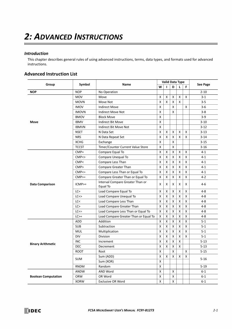
2: ADVANCED INSTRUCTIONS
IntroductionThis chapter describes general rules of using advanced instructions, terms, data types, and formats used for advanced instructions.
Advanced Instruction List
Group Symbol NameValid Data Type
See PageW I D L F
NOP NOP No Operation 2‐10
Move
MOV Move X X X X X 3‐1
MOVN Move Not X X X X 3‐5
IMOV Indirect Move X X X 3‐6
IMOVN Indirect Move Not X X 3‐8
BMOV Block Move X 3‐9
IBMV Indirect Bit Move X 3‐10
IBMVN Indirect Bit Move Not X 3‐12
NSET N Data Set X X X X X 3‐13
NRS N Data Repeat Set X X X X X 3‐14
XCHG Exchange X X 3‐15
TCCST Timer/Counter Current Value Store X X 3‐16
Data Comparison
CMP= Compare Equal To X X X X X 4‐1
CMP<> Compare Unequal To X X X X X 4‐1
CMP< Compare Less Than X X X X X 4‐1
CMP> Compare Greater Than X X X X X 4‐1
CMP<= Compare Less Than or Equal To X X X X X 4‐1
CMP>= Compare Greater Than or Equal To X X X X X 4‐2
ICMP>=Interval Compare Greater Than or Equal To
X X X X X 4‐6
LC= Load Compare Equal To X X X X X 4‐8
LC<> Load Compare Unequal To X X X X X 4‐8
LC< Load Compare Less Than X X X X X 4‐8
LC> Load Compare Greater Than X X X X X 4‐8
LC<= Load Compare Less Than or Equal To X X X X X 4‐8
LC>= Load Compare Greater Than or Equal To X X X X X 4‐8
Binary Arithmetic
ADD Addition X X X X X 5‐1
SUB Subtraction X X X X X 5‐1
MUL Multiplication X X X X X 5‐1
DIV Division X X X X X 5‐1
INC Increment X X X X 5‐13
DEC Decrement X X X X 5‐13
ROOT Root X X X 5‐15
SUMSum (ADD) X X X X X
5‐16Sum (XOR) X
RNDM Random X 5‐19
Boolean Computation
ANDW AND Word X X 6‐1
ORW OR Word X X 6‐1
XORW Exclusive OR Word X X 6‐1
FC5A MICROSMART USER’S MANUAL FC9Y‐B1273 2‐1
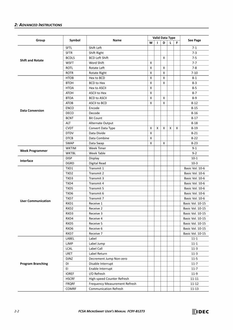
2: ADVANCED INSTRUCTIONS
Shift and Rotate
SFTL Shift Left 7‐1
SFTR Shift Right 7‐3
BCDLS BCD Left Shift X 7‐5
WSFT Word Shift X 7‐7
ROTL Rotate Left X X 7‐8
ROTR Rotate Right X X 7‐10
Data Conversion
HTOB Hex to BCD X X 8‐1
BTOH BCD to Hex X X 8‐3
HTOA Hex to ASCII X 8‐5
ATOH ASCII to Hex X 8‐7
BTOA BCD to ASCII X X 8‐9
ATOB ASCII to BCD X X 8‐12
ENCO Encode 8‐15
DECO Decode 8‐16
BCNT Bit Count 8‐17
ALT Alternate Output 8‐18
CVDT Convert Data Type X X X X X 8‐19
DTDV Data Divide X 8‐21
DTCB Data Combine X 8‐22
SWAP Data Swap X X 8‐23
Week ProgrammerWKTIM Week Timer 9‐1
WKTBL Week Table 9‐2
InterfaceDISP Display 10‐1
DGRD Digital Read 10‐3
User Communication
TXD1 Transmit 1 Basic Vol. 10‐6
TXD2 Transmit 2 Basic Vol. 10‐6
TXD3 Transmit 3 Basic Vol. 10‐6
TXD4 Transmit 4 Basic Vol. 10‐6
TXD5 Transmit 5 Basic Vol. 10‐6
TXD6 Transmit 6 Basic Vol. 10‐6
TXD7 Transmit 7 Basic Vol. 10‐6
RXD1 Receive 1 Basic Vol. 10‐15
RXD2 Receive 2 Basic Vol. 10‐15
RXD3 Receive 3 Basic Vol. 10‐15
RXD4 Receive 4 Basic Vol. 10‐15
RXD5 Receive 5 Basic Vol. 10‐15
RXD6 Receive 6 Basic Vol. 10‐15
RXD7 Receive 7 Basic Vol. 10‐15
Program Branching
LABEL Label 11‐1
LJMP Label Jump 11‐1
LCAL Label Call 11‐3
LRET Label Return 11‐3
DJNZ Decrement Jump Non‐zero 11‐5
DI Disable Interrupt 11‐7
EI Enable Interrupt 11‐7
IOREF I/O Refresh 11‐9
HSCRF High‐speed Counter Refresh 11‐11
FRQRF Frequency Measurement Refresh 11‐12
COMRF Communication Refresh 11‐13
Group Symbol NameValid Data Type
See PageW I D L F
2‐2 FC5A MICROSMART USER’S MANUAL FC9Y‐B1273
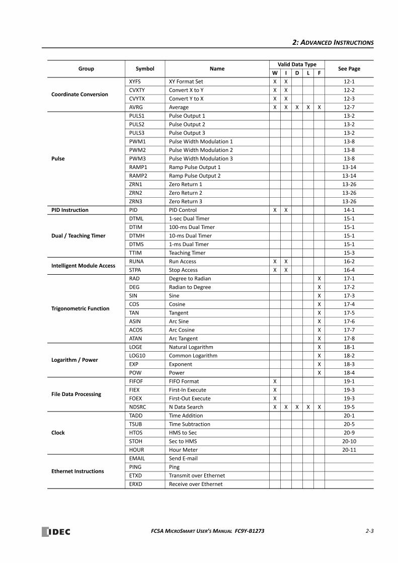
2: ADVANCED INSTRUCTIONS
Coordinate Conversion
XYFS XY Format Set X X 12‐1
CVXTY Convert X to Y X X 12‐2
CVYTX Convert Y to X X X 12‐3
AVRG Average X X X X X 12‐7
Pulse
PULS1 Pulse Output 1 13‐2
PULS2 Pulse Output 2 13‐2
PULS3 Pulse Output 3 13‐2
PWM1 Pulse Width Modulation 1 13‐8
PWM2 Pulse Width Modulation 2 13‐8
PWM3 Pulse Width Modulation 3 13‐8
RAMP1 Ramp Pulse Output 1 13‐14
RAMP2 Ramp Pulse Output 2 13‐14
ZRN1 Zero Return 1 13‐26
ZRN2 Zero Return 2 13‐26
ZRN3 Zero Return 3 13‐26
PID Instruction PID PID Control X X 14‐1
Dual / Teaching Timer
DTML 1‐sec Dual Timer 15‐1
DTIM 100‐ms Dual Timer 15‐1
DTMH 10‐ms Dual Timer 15‐1
DTMS 1‐ms Dual Timer 15‐1
TTIM Teaching Timer 15‐3
Intelligent Module AccessRUNA Run Access X X 16‐2
STPA Stop Access X X 16‐4
Trigonometric Function
RAD Degree to Radian X 17‐1
DEG Radian to Degree X 17‐2
SIN Sine X 17‐3
COS Cosine X 17‐4
TAN Tangent X 17‐5
ASIN Arc Sine X 17‐6
ACOS Arc Cosine X 17‐7
ATAN Arc Tangent X 17‐8
Logarithm / Power
LOGE Natural Logarithm X 18‐1
LOG10 Common Logarithm X 18‐2
EXP Exponent X 18‐3
POW Power X 18‐4
File Data Processing
FIFOF FIFO Format X 19‐1
FIEX First‐In Execute X 19‐3
FOEX First‐Out Execute X 19‐3
NDSRC N Data Search X X X X X 19‐5
Clock
TADD Time Addition 20‐1
TSUB Time Subtraction 20‐5
HTOS HMS to Sec 20‐9
STOH Sec to HMS 20‐10
HOUR Hour Meter 20‐11
Ethernet Instructions
EMAIL Send E‐mail
PING Ping
ETXD Transmit over Ethernet
ERXD Receive over Ethernet
Group Symbol NameValid Data Type
See PageW I D L F
FC5A MICROSMART USER’S MANUAL FC9Y‐B1273 2‐3
2: ADVANCED INSTRUCTIONS
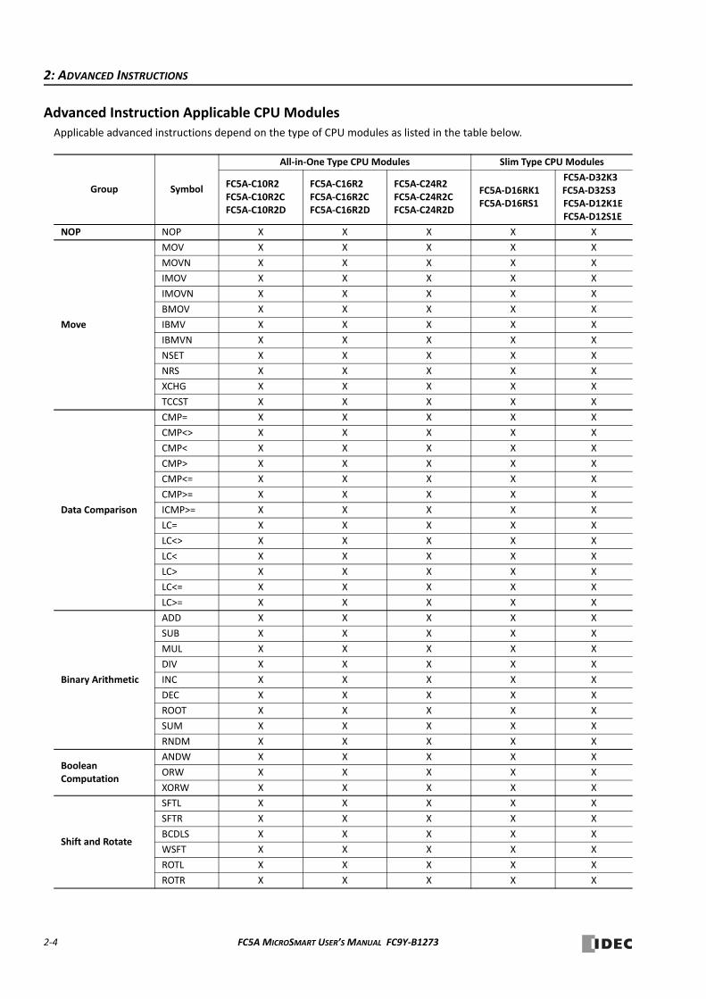
Advanced Instruction Applicable CPU ModulesApplicable advanced instructions depend on the type of CPU modules as listed in the table below.
Group Symbol
All‐in‐One Type CPU Modules Slim Type CPU Modules
FC5A‐C10R2FC5A‐C10R2CFC5A‐C10R2D
FC5A‐C16R2FC5A‐C16R2CFC5A‐C16R2D
FC5A‐C24R2FC5A‐C24R2CFC5A‐C24R2D
FC5A‐D16RK1FC5A‐D16RS1
FC5A‐D32K3FC5A‐D32S3FC5A‐D12K1EFC5A‐D12S1E
NOP NOP X X X X X
Move
MOV X X X X X
MOVN X X X X X
IMOV X X X X X
IMOVN X X X X X
BMOV X X X X X
IBMV X X X X X
IBMVN X X X X X
NSET X X X X X
NRS X X X X X
XCHG X X X X X
TCCST X X X X X
Data Comparison
CMP= X X X X X
CMP<> X X X X X
CMP< X X X X X
CMP> X X X X X
CMP<= X X X X X
CMP>= X X X X X
ICMP>= X X X X X
LC= X X X X X
LC<> X X X X X
LC< X X X X X
LC> X X X X X
LC<= X X X X X
LC>= X X X X X
Binary Arithmetic
ADD X X X X X
SUB X X X X X
MUL X X X X X
DIV X X X X X
INC X X X X X
DEC X X X X X
ROOT X X X X X
SUM X X X X X
RNDM X X X X X
BooleanComputation
ANDW X X X X X
ORW X X X X X
XORW X X X X X
Shift and Rotate
SFTL X X X X X
SFTR X X X X X
BCDLS X X X X X
WSFT X X X X X
ROTL X X X X X
ROTR X X X X X
2‐4 FC5A MICROSMART USER’S MANUAL FC9Y‐B1273
2: ADVANCED INSTRUCTIONS
Note 1: Not available on FC5A‐D12K1E/S1E.
Note 2: Not available on FC5A‐C24R2D.
Group Symbol
All‐in‐One Type CPU Modules Slim Type CPU Modules
FC5A‐C10R2FC5A‐C10R2CFC5A‐C10R2D
FC5A‐C16R2FC5A‐C16R2CFC5A‐C16R2D
FC5A‐C24R2FC5A‐C24R2CFC5A‐C24R2D
FC5A‐D16RK1FC5A‐D16RS1
FC5A‐D32K3FC5A‐D32S3FC5A‐D12K1EFC5A‐D12S1E
Data Conversion
HTOB X X X X X
BTOH X X X X X
HTOA X X X X X
ATOH X X X X X
BTOA X X X X X
ATOB X X X X X
ENCO X X X X X
DECO X X X X X
BCNT X X X X X
ALT X X X X X
CVDT X X X X X
DTDV X X X X X
DTCB X X X X X
SWAP X X X X X
Week ProgrammerWKTIM X X X X X
WKTBL X X X X X
InterfaceDISP X X X
DGRD X X X
User Communication
TXD1 X X X X X (Note 1)
TXD2 X X X X X
TXD3 X (Note 2) X X
TXD4 X (Note 2) X X
TXD5 X (Note 2) X X
TXD6 X X
TXD7 X X
RXD1 X X X X X (Note 1)
RXD2 X X X X X
RXD3 X (Note 2) X X
RXD4 X (Note 2) X X
RXD5 X (Note 2) X X
RXD6 X X
RXD7 X X
ProgramBranching
LABEL X X X X X
LJMP X X X X X
LCAL X X X X X
LRET X X X X X
DJNZ X X X X X
DI X X X X X
EI X X X X X
IOREF X X X X X
HSCRF X X X X X
FRQRF X X X X X
COMRF X (Note 2) X X
Coordinate Conversion
XYFS X X X X X
CVXTY X X X X X
CVYTX X X X X X
AVRG X X X X X
FC5A MICROSMART USER’S MANUAL FC9Y‐B1273 2‐5

2: ADVANCED INSTRUCTIONS
Note 1: Not available on FC5A‐C24R2D.
Note 2: Ethernet instructions can only be used with FC5A‐D12K1E and FC5A‐D12S1E.
Group Symbol
All‐in‐One Type CPU Modules Slim Type CPU Modules
FC5A‐C10R2FC5A‐C10R2CFC5A‐C10R2D
FC5A‐C16R2FC5A‐C16R2CFC5A‐C16R2D
FC5A‐C24R2FC5A‐C24R2CFC5A‐C24R2D
FC5A‐D16RK1FC5A‐D16RS1
FC5A‐D32K3FC5A‐D32S3FC5A‐D12K1EFC5A‐D12S1E
Pulse
PULS1 X X
PULS2 X X
PULS3 X
PWM1 X X
PWM2 X X
PWM3 X
RAMP1 X X
RAMP2 X
ZRN1 X X
ZRN2 X X
ZRN3 X
PID Instruction PID X X X
Dual / Teaching Timer
DTML X X X X X
DTIM X X X X X
DTMH X X X X X
DTMS X X X X X
TTIM X X X X X
Intelligent Module Access
RUNA X (Note 1) X X
STPA X (Note 1) X X
Trigonometric Function
RAD X X X X X
DEG X X X X X
SIN X X X X X
COS X X X X X
TAN X X X X X
ASIN X X X X X
ACOS X X X X X
ATAN X X X X X
Logarithm / Power
LOGE X X X X X
LOG10 X X X X X
EXP X X X X X
POW X X X X X
File Data Processing
FIFOF X X X X X
FIEX X X X X X
FOEX X X X X X
NDSRC X X X X X
Clock
TADD X X X X X
TSUB X X X X X
HTOS X X X X X
STOH X X X X X
HOUR X X X X X
Ethernet Instructions
EMAIL X (Note 2)
PING X (Note 2)
ETXD X (Note 2)
ERXD X (Note 2)
2‐6 FC5A MICROSMART USER’S MANUAL FC9Y‐B1273
2: ADVANCED INSTRUCTIONS
Structure of an Advanced Instruction
Input Condition for Advanced InstructionsAlmost all advanced instructions must be preceded by a contact, except NOP (no operation), LABEL (label), LRET (label return), and STPA (stop access) instructions. The input condition can be programmed using a bit device such as input, output, internal relay, or shift register. Timer and counter can also be used as an input condition to turn on the contact when the timer times out or the counter counts out.
While the input condition is on, the advanced instruction is executed in each scan. To execute the advanced instruction only at the rising or falling edge of the input, use the SOTU or SOTD instruction.
While the input condition is off, the advanced instruction is not executed and device statuses are held.
Source and Destination DevicesThe source and destination devices specify 16‐ or 32‐bit data, depending on the selected data type. When a bit device such as input, output, internal relay, or shift register is designated as a source or destination device, 16 or 32 points start‐ing with the designated number are processed as source or destination data. When a word device such as timer or coun‐ter is designated as a source device, the current value is read as source data. When a timer or counter is designated as a destination device, the result of the advanced instruction is set to the preset value for the timer or counter. When a data register is designated as a source or destination device, the data is read from or written to the designated data register.
Using Timer or Counter as Source DeviceSince all timer instructions—TML (1‐sec timer), TIM (100‐ms timer), TMH (10‐ms timer), and TMS (1‐ms timer)—subtract from the preset value, the current value is decremented from the preset value and indicates the remaining time. As described above, when a timer is designated as a source device of an advanced instruction, the current value, or the remaining time, of the timer is read as source data. Adding counters CNT start counting at 0, and the current value is incremented up to the preset value. Reversible counters CDP and CUD start counting at the preset value and the current value is incremented or decremented from the preset value. When any counter is designated as a source device of an advanced instruction, the current value is read as source data.
Using Timer or Counter as Destination DeviceAs described above, when a timer or counter is designated as a destination device of an advanced instruction, the result of the advanced instruction is set to the preset value of the timer or counter. Timer and counter preset values can be 0 through 65535.
When a timer or counter preset value is designated using a data register, the timer or counter cannot be designated as a destination of an advanced instruction. When executing such an advanced instruction, a user program execution error will result. For details of user program execution error, see page 13‐2 (Basic Vol.).
Note: When a user program execution error occurs, the result is not set to the destination.
Repeat Designation
Specifies whether repeat is used for the device or not.
Repeat Cycles
Specifies the quantity of repeat cycles: 1 through 99.
I0
S1 R*****
REP**
D1 R*****
Opcode
The opcode is a symbol to identify the advanced instruction.
Data Type
Specifies the word (W), integer (I), double word (D), long (L), or float (F) data type.
Source Device
The source device specifies the 16‐ or 32‐bit data to be pro‐cessed by the advanced instruction. Some advanced instruc‐tions require two source devices.
Destination Device
The destination device specifies the 16‐ or 32‐bit data to store the result of the advanced instruction. Some advanced instructions require two destination devices.
Opcode
Source Device
Repeat Cycles
Destination Device
Repeat
MOV(W)
Data TypeDesignation
I0
REPS1 –D10
D1 –D20
SOTU MOV(W)
FC5A MICROSMART USE
R’S MANUAL FC9Y‐B1273 2‐7
2: ADVANCED INSTRUCTIONS
Data Types for Advanced Instructions (Integer Type)When using move, data comparison, binary arithmetic, Boolean computation, bit shift/rotate, data conversion, and coor‐dinate conversion instructions, data types can be selected from word (W), integer (I), double word (D), long (L), or float (F). For other advanced instructions, the data is processed in units of 16‐bit word.
Decimal Values and Hexadecimal Storage (Word, Integer, Double, and Long Data Types)
The following table shows hexadecimal equivalents which are stored in the CPU, as a result of addition and subtraction of the decimal values shown:
Data Type Symbol BitsQuantity of Data Registers Used
Range of Decimal Values
Word (Unsigned 16 bits) W 16 bits 1 0 to 65,535
Integer (Signed 15 bits) I 16 bits 1 –32,768 to 32,767
Double Word (Unsigned 32 bits) D 32 bits 2 0 to 4,294,967,295
Long (Signed 31 bits) L 32 bits 2 –2,147,483,648 to 2,147,483,647
Float (Floating point) F 32 bits 2 –3.4028231038 to 3.4028231038
Data Type Result of Addition Hexadecimal Storage Result of Subtraction Hexadecimal Storage
Word
065535131071
0000FFFF
(CY) FFFF
655350–1
–65535–65536
FFFF0000
(BW) FFFF(BW) 0001(BW) 0000
Integer
6553432768327670–1
–32767–32768–32769–65535
(CY) 7FFE(CY) 00007FFF0000FFFF80018000
(CY) FFFF(CY) 8001
6553432768327670–1
–32767–32768–32769–65535
(BW) 7FFE(BW) 0000
7FFF0000FFFF80018000
(BW) FFFF(BW) 8001
Double Word
042949672958589934591
00000000FFFFFFFF
(CY) FFFFFFFF
42949672950–1
–4294967295–4294967296
FFFFFFFF00000000
(BW) FFFFFFFF(BW) 00000001(BW) 00000000
Long
429496729421474836482147483647
0–1
–2147483647–2147483648–2147483649–4294967295
(CY) 7FFFFFFE(CY) 00000000
7FFFFFFF00000000FFFFFFFF8000000180000000
(CY) FFFFFFFF(CY) 80000001
429496729421474836482147483647
0–1
–2147483647–2147483648–2147483649–4294967295
(BW) 7FFFFFFE(BW) 00000000
7FFFFFFF00000000FFFFFFFF8000000180000000
(BW) FFFFFFFF(BW) 80000001
2‐8 FC5A MICROSMART USER’S MANUAL FC9Y‐B1273

2: ADVANCED INSTRUCTIONS
Floating‐Point Data Format
The FC5A MicroSmart can specify the floating‐point data type (F) for advanced instructions. Like the double word (D) and long integer (L) data types, the floating‐point data type also uses two consecutive data registers to execute advanced instructions. The FC5A MicroSmart supports the floating‐point data based on the single storage format of the IEEE (The Institute of Electrical and Electronics Engineers) Standard 754.
Single Storage Format
The IEEE single format consists of three fields: a 23‐bit fraction, f; an 8‐bit biased exponent, e; and 1‐bit sign, s. These fields are stored contiguously in one 32‐bit word, as shown in the figure below. Bits 0:22 contain the 23‐bit fraction, f, with bit 0 being the least significant bit of the fraction and bit 22 being the most significant; bits 23:30 contain the 8‐bit biased exponent, e, with bit 23 being the least significant bit of the biased exponent and bit 30 being the most significant; and the highest‐order bit 31 contains the sign bit, s.
The table below shows the correspondence between the values of the three constituent fields s, e, and f and the value represented by the single format bit pattern. When any value out of the bit pattern is entered to the advanced instruction or when execution of advanced instructions, such as division by zero, has produced any value out of the bit pattern, a user program execution error will result, turning on special internal relay M8004 and the ERR LED on the CPU module.
Carry and Borrow in Floating‐Point Data Processing
When advanced instructions involving floating‐point data are executed, special internal relay M8003 (carry and borrow) is updated.
Single Format Bit Patters Value
0 < e < 255 (–1)s 2e–127 1.f (normal numbers)
e = 0; f = 0 (all bits in f are zero) (–1)s 2e–127 0.0 (signed zero)
M8003 Execution Result Value
1 Overflow (out of the range between –3.4028231038 and 3.4028231038)
1 0 Not zero (within the range between –1.17549510–38 and 1.17549510–38)
0 0 Zero
s e[30:23] f[22:0]
31 30 23 22 0
Single Storage Format
23‐bit fraction8‐bit biased exponent
Sign bit (0: positive, 1: negative)
0
0
–1.17549510–38
M8003 1 1
1.17549510–380–3.4028231038
0
Execution Result
1
Overflow
0 1
3.4028231038
Overflow
Not Zero
FC5A MICROSMART USER’S MANUAL FC9Y‐B1273 2‐9
2: ADVANCED INSTRUCTIONS
Double‐word Devices in Data Registers
When the double‐word data type is selected for the source or destination device, the data is loaded from or stored to two consecutive data registers. The order of the two devices depends on the device type.
When a data register, timer, or counter is selected as a double‐word device, the high‐word data is loaded from or stored to the first device selected. The low‐word data is loaded from or stored to the subsequent device.
Example: When data register D10 is designated as a double‐word source device and data register D20 is designated as a double‐word destination device, the data is loaded from or stored to two consecutive data registers as illustrated below.
Note: The above example is the default setting of the FC5A MicroSmart. The order of two devices can be selected on CPU modules with system program version 110 or higher. See page 5‐46 (Basic Vol.).
Discontinuity of Device AreasEach device area is discrete and does not continue, for example, from input to output or from output to internal relay. In addition, special internal relays M8000 through M8157 (all‐in‐one type CPU) or M8317 (slim type CPU) are in a separate area from internal relays M0 through M2557. Data registers D0 through D1999, expansion data registers D2000 through D7999 (slim type CPU only), and special data registers D8000 through D8199 (all‐in‐one type CPU) or D8499 (slim type CPU) are in separate areas and do not continue with each other.
Advanced instructions execute operation only on the available devices in the valid area. If a user program syntax error is found during programming, WindLDR rejects the program instruction and shows an error message.
NOP (No Operation)
Details of all other advanced instructions are described in the following chapters.
305419896
Double‐word Data
High Word D10
(12345678h)
Source Device
4660(1234h)
Low Word D1122136(5678h)
High Word D204660
(1234h)
Low Word D2122136(5678h)
Destination Device
The internal relay ends at M2557. Since the MOV (move) instruction reads 16 internal relays, the last internal relay exceeds the valid range, resulting in a user program syntax error.M8125
REPS1 –M2550
D1 –D0
MOV(W)
This program results in a user program syntax error. The destination of the DIV (division) instruction requires two data registers D1999 and D2000. Since D2000 exceeds the valid range, a user program syntax error occurs.
I0
REPS1 –D100
S2 –D200
DIV(W) D1 –D1999
The MOV (move) instruction sets data of data register D0 to 16 outputs Q610 through Q627 in the first repeat cycle. The destination of the second cycle is the next 16 outputs Q630 through Q647, which are invalid, resulting in a user pro‐gram syntax error.
For details about repeat operations of each advanced instruction, see the fol‐lowing chapters.
M8125
REP2
S1 –D0
D1 RQ610
MOV(W)
No operation is executed by the NOP instruction.
The NOP instruction may serve as a place holder. Another use would be to add a delay to the CPU scan time, in order to simulate communication with a machine or application, for debugging purposes.
The NOP instruction does not require an input and device.
NOP
2‐10 FC5A MICROSMART USER’S MANUAL FC9Y‐B1273

3: MOVE INSTRUCTIONS
IntroductionData can be moved using the MOV (move), MOVN (move not), IMOV (indirect move), or IMOVN (indirect move not) instruction. The moved data is 16‐ or 32‐bit data, and the repeat operation can also be used to increase the quantity of data moved. In the MOV or MOVN instruction, the source and destination device are designated by S1 and D1 directly. In the IMOV or IMOVN instruction, the source and destination device are determined by the offset values designated by S2 and D2 added to source device S1 and destination device D1.
The BMOV (block move) instruction is useful to move consecutive blocks of timer, counter, and data register values.
The IBMV (indirect bit move) and IBMVN (indirect bit move not) instructions move one bit of data from a source device to a destination device. Both devices are determined by adding an offset to the device.
NSET (N data set) and NRS (N data repeat set) instructions can be used to set values to a group of devices. The XCHG (exchange) instruction is used to swap word or double‐word data between two devices. The current values of timer or counter can be changed using the TCCST (timer/counter current value store) instruction.
Since the move instructions are executed in each scan while input is on, a pulse input from a SOTU or SOTD instruction should be used as required.
MOV (Move)
Applicable CPU Modules
Valid Devices
For the valid device address range, see pages 6‐1 and 6‐2 (Basic Vol.).
Internal relays M0 through M2557 can be designated as D1. Special internal relays cannot be designated as D1.Source device can be both internal relays M0 through M2557 and special internal relays M8000 through M8157 (all‐in‐one type CPU) or M8317 (slim type CPU).
When T (timer) or C (counter) is used as S1, the timer/counter current value (TC or CC) is read out. When T (timer) or C (counter) is used as D1, the data is written in as a preset value (TP or CP) which can be 0 through 65535.
When F (float) data type is selected, only data register and constant can be designated as S1, and only data register can be designated as D1.
When F (float) data type is selected and S1 does not comply with the normal floating‐point format, a user program execution error will result, turning on special internal relay M8004 and ERR LED on the CPU module.
Valid Data Types
FC5A‐C10R2/C/D FC5A‐C16R2/C/D FC5A‐C24R2/C/D FC5A‐D16RK1/RS1 FC5A‐D32K3/S3 FC5A‐D12K1E/S1E
X X X X X X
Device Function I Q M R T C D Constant Repeat
S1 (Source 1) First device address to move X X X X X X X X 1‐99
D1 (Destination 1) First device address to move to — X X X X X — 1‐99
W (word) X
I (integer) X
D (double word) X
L (long) X
F (float) X
S1 D1When input is on, 16‐ or 32‐bit data from device designated by S1 is moved to device designated by D1.
The float data type is available on upgraded CPU modules with system program version 200 or higher.
REP**
S1(R)*****
D1(R)*****
MOV(*)
When a bit device such as I (input), Q (output), M (internal relay), or R (shift register) is designated as the source or destination, 16 points (word or integer data type) or 32 points (double‐word or long data type) are used. When repeat is designated for a bit device, the quantity of device bits increases in 16‐ or 32‐point increments.
When a word device such as T (timer), C (counter), or D (data register) is designated as the source or destination, 1 point (word or integer data type) or 2 points (double‐word, long, or float data type) are used. When repeat is designated for a word device, the quantity of device words increases in 1‐ or 2‐point increments.
FC5A MICROSMART USER’S MANUAL FC9Y‐B1273 3‐1
3: MOVE INSTRUCTIONS
Examples: MOV
Data Type: Word
Data Type: Word
Data move operation for the integer data type is the same as for the word data type.
Data Type: Double Word
Data move operation for the long data type is the same as for the double‐word data type.
Data Type: Word
Data Type: Double Word
Double‐word Data Move in Data Registers
When a data register, timer, or counter is selected as a double‐word device, the upper‐word data is loaded from or stored to the first device selected. The lower‐word data is loaded from or stored to the subsequent device.
I2
REPD10 M0When input I2 is on, the data in data register D10 designated by source device S1 is moved to 16 internal relays starting with M0 designated by destination device D1.
12345D10
S1 –D10
D1 –M0
M0 through M7, M10 through M17
The data in the source data register is converted into 16‐bit binary data, and the ON/OFF statuses of the 16 bits are moved to internal relays M0 through M7 and M10 through M17. M0 is the LSB (least significant bit). M17 is the MSB (most significant bit).
MOV(W)
0 1 0010 0 0 0 1 0010 1 1
MSB
M0
LSB
M17 M7M10
I0
REP810 D2When input I0 is on, constant 810 designated by source device S1 is moved to data register D2 desig‐nated by destination device D1.
D1
D0
810D2 810
S1 –810
D1 –D2
MOV(W)
I0
REP810 D2∙D3When input I0 is on, constant 810 designated by source device S1 is moved to data registers D2 and D3 designated by destination device D1.
D1
D0
0D2 0
S1 –810
D1 –D2
MOV(D)
810D3 810
I1
REPD10 D2When input I1 is on, the data in data register D10 designated by source device S1 is moved to data register D2 designated by destination device D1.
D1
D0
930D2
930D10
S1 –D10
D1 –D2
MOV(W)
I1
REPD10∙D11 D2∙D3When input I1 is on, the data in data registers D10 and D11 designated by source device S1 is moved to data registers D2 and D3 designated by destination device D1.
D1
D0
D2
Double‐D10
S1 –D10
D1 –D2
MOV(D)
D3
D11wordData
305419896
Double‐word
(12345678h)
High Word D04660
(1234h)
Low Word D122136(5678h)
I1
REPS1 –305419896
D1 –D0
MOV(D) Source Data
Data Move to Data RegistersDouble‐word Destination Device: Data Register
3‐2 FC5A MICROSMART USER’S MANUAL FC9Y‐B1273
3: MOVE INSTRUCTIONS
Repeat Operation in the Move Instructions
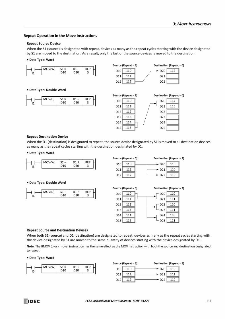
Repeat Source Device
When the S1 (source) is designated with repeat, devices as many as the repeat cycles starting with the device designated by S1 are moved to the destination. As a result, only the last of the source devices is moved to the destination.
• Data Type: Word
• Data Type: Double Word
Repeat Destination Device
When the D1 (destination) is designated to repeat, the source device designated by S1 is moved to all destination devices as many as the repeat cycles starting with the destination designated by D1.
• Data Type: Word
• Data Type: Double Word
Repeat Source and Destination Devices
When both S1 (source) and D1 (destination) are designated to repeat, devices as many as the repeat cycles starting with the device designated by S1 are moved to the same quantity of devices starting with the device designated by D1.
Note: The BMOV (block move) instruction has the same effect as the MOV instruction with both the source and destination designated to repeat.
• Data Type: Word
111D11
110D10
112D12
D21
112D20
D22
Source (Repeat = 3) Destination (Repeat = 0)
I1
REP3
S1 RD10
D1 –D20
MOV(W)
111D11
110D10
112D12
115D21
114D20
D22
Source (Repeat = 3) Destination (Repeat = 0)
I2
REP3
S1 RD10
D1 –D20
MOV(D)
113D13 D23
114D14
115D15
D24
D25
111D11
110D10
112D12
110D21
110D20
110D22
Source (Repeat = 0) Destination (Repeat = 3)
I3
REP3
S1 –D10
D1 RD20
MOV(W)
111D11
110D10
112D12
111D21
110D20
110D22
Source (Repeat = 0) Destination (Repeat = 3)
I4
REP3
S1 –D10
D1 RD20
MOV(D)
113D13 111D23
114D14
115D15
110D24
111D25
111D11
110D10
112D12
111D21
110D20
112D22
Source (Repeat = 3) Destination (Repeat = 3)
I5
REP3
S1 RD10
D1 RD20
MOV(W)
FC5A MICROSMART USER’S MANUAL FC9Y‐B1273 3‐3
3: MOVE INSTRUCTIONS
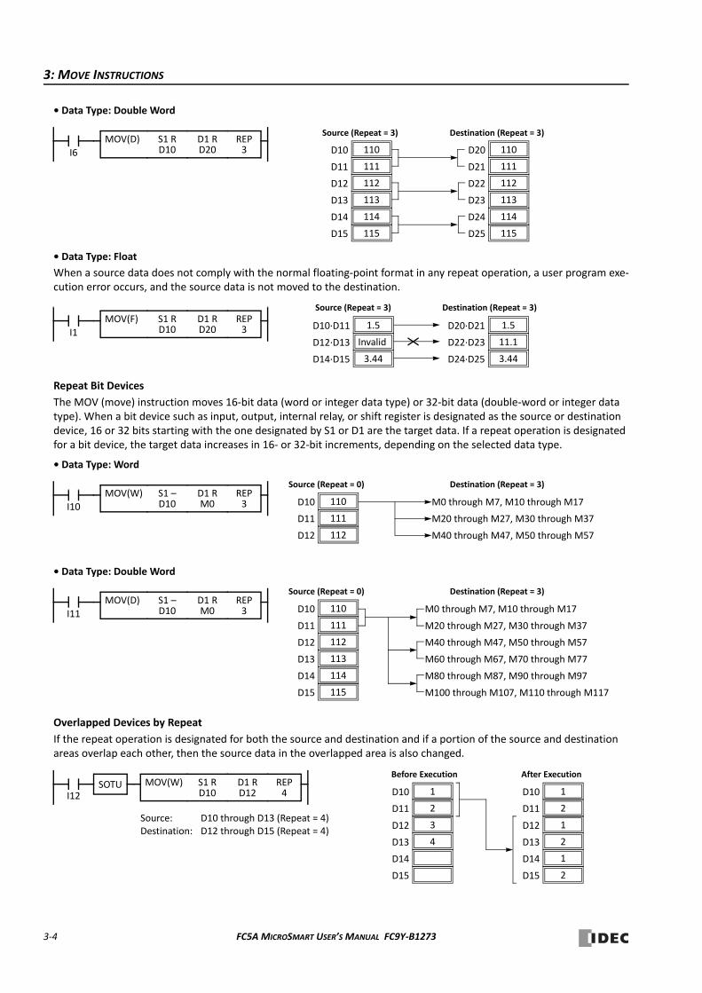
• Data Type: Double Word
• Data Type: Float
When a source data does not comply with the normal floating‐point format in any repeat operation, a user program exe‐cution error occurs, and the source data is not moved to the destination.
Repeat Bit Devices
The MOV (move) instruction moves 16‐bit data (word or integer data type) or 32‐bit data (double‐word or integer data type). When a bit device such as input, output, internal relay, or shift register is designated as the source or destination device, 16 or 32 bits starting with the one designated by S1 or D1 are the target data. If a repeat operation is designated for a bit device, the target data increases in 16‐ or 32‐bit increments, depending on the selected data type.
• Data Type: Word
• Data Type: Double Word
Overlapped Devices by Repeat
If the repeat operation is designated for both the source and destination and if a portion of the source and destination areas overlap each other, then the source data in the overlapped area is also changed.
111D11
110D10
112D12
111D21
110D20
112D22
Source (Repeat = 3) Destination (Repeat = 3)
I6
REP3
S1 RD10
D1 RD20
MOV(D)
113D13 113D23
114D14
115D15
114D24
115D25
Invalid D12∙D13
1.5D10∙D11
3.44D14∙D15
11.1D22∙D23
1.5D20∙D21
3.44D24∙D25
Source (Repeat = 3) Destination (Repeat = 3)
I1
REP3
S1 RD10
D1 RD20
MOV(F)
111D11
110D10
112D12
M20 through M27, M30 through M37
M0 through M7, M10 through M17
M40 through M47, M50 through M57
Source (Repeat = 0) Destination (Repeat = 3)
I10
REP3
S1 –D10
D1 RM0
MOV(W)
111D11
110D10
112D12
M20 through M27, M30 through M37
M0 through M7, M10 through M17
M40 through M47, M50 through M57
Source (Repeat = 0) Destination (Repeat = 3)
I11
REP3
S1 –D10
D1 RM0
MOV(D)
114D14
113D13
115D15
M80 through M87, M90 through M97
M60 through M67, M70 through M77
M100 through M107, M110 through M117
2D11
1D10
3D12
4D13
D14
D15
2D11
1D10
1D12
2D13
1D14
2D15
Before Execution After Execution
Source: D10 through D13 (Repeat = 4)Destination: D12 through D15 (Repeat = 4)
I12
REP4
S1 RD10
D1 RD12
MOV(W)SOTU
3‐4 FC5A MICROSMART USER’S MANUAL FC9Y‐B1273
3: MOVE INSTRUCTIONS
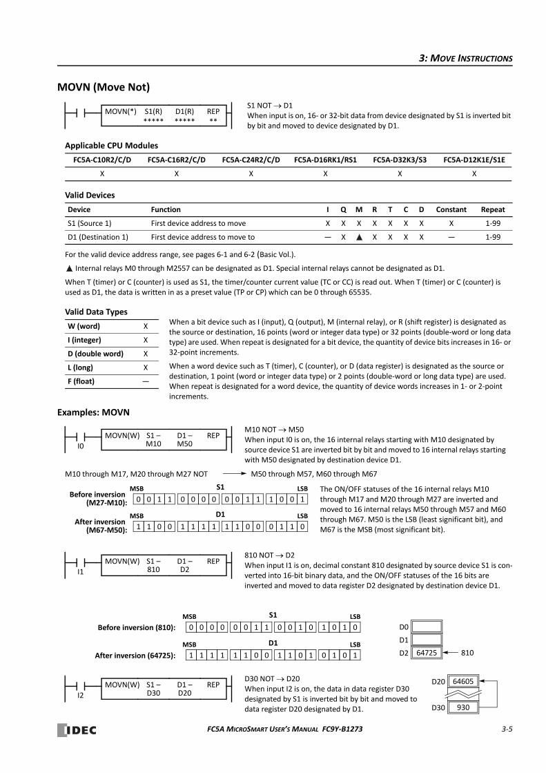
MOVN (Move Not)
Applicable CPU Modules
Valid Devices
For the valid device address range, see pages 6‐1 and 6‐2 (Basic Vol.).
Internal relays M0 through M2557 can be designated as D1. Special internal relays cannot be designated as D1.
When T (timer) or C (counter) is used as S1, the timer/counter current value (TC or CC) is read out. When T (timer) or C (counter) is used as D1, the data is written in as a preset value (TP or CP) which can be 0 through 65535.
Valid Data Types
Examples: MOVN
FC5A‐C10R2/C/D FC5A‐C16R2/C/D FC5A‐C24R2/C/D FC5A‐D16RK1/RS1 FC5A‐D32K3/S3 FC5A‐D12K1E/S1E
X X X X X X
Device Function I Q M R T C D Constant Repeat
S1 (Source 1) First device address to move X X X X X X X X 1‐99
D1 (Destination 1) First device address to move to — X X X X X — 1‐99
W (word) X
I (integer) X
D (double word) X
L (long) X
F (float) —
S1 NOT D1When input is on, 16‐ or 32‐bit data from device designated by S1 is inverted bit by bit and moved to device designated by D1.
REP**
S1(R)*****
D1(R)*****
MOVN(*)
When a bit device such as I (input), Q (output), M (internal relay), or R (shift register) is designated as the source or destination, 16 points (word or integer data type) or 32 points (double‐word or long data type) are used. When repeat is designated for a bit device, the quantity of device bits increases in 16‐ or 32‐point increments.
When a word device such as T (timer), C (counter), or D (data register) is designated as the source or destination, 1 point (word or integer data type) or 2 points (double‐word or long data type) are used. When repeat is designated for a word device, the quantity of device words increases in 1‐ or 2‐point increments.
M10 NOT M50When input I0 is on, the 16 internal relays starting with M10 designated by source device S1 are inverted bit by bit and moved to 16 internal relays starting with M50 designated by destination device D1.
M10 through M17, M20 through M27 NOT M50 through M57, M60 through M67
The ON/OFF statuses of the 16 internal relays M10 through M17 and M20 through M27 are inverted and moved to 16 internal relays M50 through M57 and M60 through M67. M50 is the LSB (least significant bit), and M67 is the MSB (most significant bit).
Before inversion 0 1 0010 0 0 0 1 0010 1 1
MSB LSBS1
After inversion 1 0 1101 1 1 1 0 1101 0 0
MSB LSBD1
I0
REPS1 –M10
D1 –M50
MOVN(W)
(M27‐M10):
(M67‐M50):
810 NOT D2When input I1 is on, decimal constant 810 designated by source device S1 is con‐verted into 16‐bit binary data, and the ON/OFF statuses of the 16 bits are inverted and moved to data register D2 designated by destination device D1.
D1
D0
64725D2 810
Before inversion (810): 0 0 1000 0 1 0 1 1000 1 0
MSB LSBS1
After inversion (64725): 1 1 0111 1 0 1 0 0111 0 1
MSB LSBD1
I1
REPS1 –810
D1 –D2
MOVN(W)
D30 NOT D20When input I2 is on, the data in data register D30 designated by S1 is inverted bit by bit and moved to data register D20 designated by D1.
64605D20
930D30
I2
REPS1 –D30
D1 –D20
MOVN(W)
FC5A MICROSMART USER’S MANUAL FC9Y‐B1273 3‐5
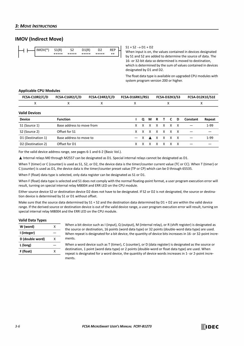
3: MOVE INSTRUCTIONS
IMOV (Indirect Move)
Applicable CPU Modules
Valid Devices
For the valid device address range, see pages 6‐1 and 6‐2 (Basic Vol.).
Internal relays M0 through M2557 can be designated as D1. Special internal relays cannot be designated as D1.
When T (timer) or C (counter) is used as S1, S2, or D2, the device data is the timer/counter current value (TC or CC). When T (timer) or C (counter) is used as D1, the device data is the timer/counter preset value (TP or CP) which can be 0 through 65535.
When F (float) data type is selected, only data register can be designated as S1 or D1.
When F (float) data type is selected and S1 does not comply with the normal floating‐point format, a user program execution error will result, turning on special internal relay M8004 and ERR LED on the CPU module.
Either source device S2 or destination device D2 does not have to be designated. If S2 or D2 is not designated, the source or destina‐tion device is determined by S1 or D1 without offset.
Make sure that the source data determined by S1 + S2 and the destination data determined by D1 + D2 are within the valid device range. If the derived source or destination device is out of the valid device range, a user program execution error will result, turning on special internal relay M8004 and the ERR LED on the CPU module.
Valid Data Types
FC5A‐C10R2/C/D FC5A‐C16R2/C/D FC5A‐C24R2/C/D FC5A‐D16RK1/RS1 FC5A‐D32K3/S3 FC5A‐D12K1E/S1E
X X X X X X
Device Function I Q M R T C D Constant Repeat
S1 (Source 1) Base address to move from X X X X X X X — 1‐99
S2 (Source 2) Offset for S1 X X X X X X X — —
D1 (Destination 1) Base address to move to — X X X X X — 1‐99
D2 (Destination 2) Offset for D1 X X X X X X X — —
W (word) X
I (integer) —
D (double word) X
L (long) —
F (float) X
S1 + S2 D1 + D2When input is on, the values contained in devices designated by S1 and S2 are added to determine the source of data. The 16‐ or 32‐bit data so determined is moved to destination, which is determined by the sum of values contained in devices designated by D1 and D2.
The float data type is available on upgraded CPU modules with system program version 200 or higher.
REP**
S1(R)*****
D1(R)*****
IMOV(*) S2*****
D2*****
When a bit device such as I (input), Q (output), M (internal relay), or R (shift register) is designated as the source or destination, 16 points (word data type) or 32 points (double‐word data type) are used. When repeat is designated for a bit device, the quantity of device bits increases in 16‐ or 32‐point incre‐ments.
When a word device such as T (timer), C (counter), or D (data register) is designated as the source or destination, 1 point (word data type) or 2 points (double‐word or float data type) are used. When repeat is designated for a word device, the quantity of device words increases in 1‐ or 2‐point incre‐ments.
3‐6 FC5A MICROSMART USER’S MANUAL FC9Y‐B1273
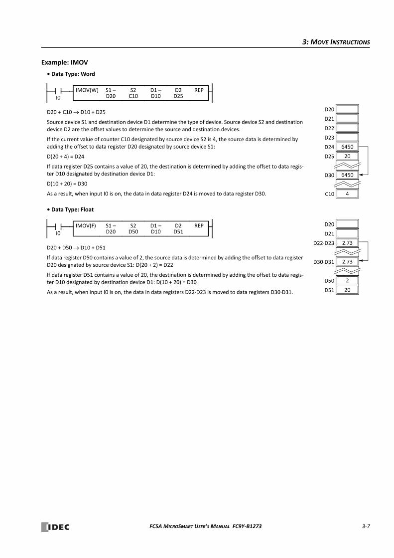
3: MOVE INSTRUCTIONS
Example: IMOV
• Data Type: Word
• Data Type: Float
D20 C10 D10 + D25
Source device S1 and destination device D1 determine the type of device. Source device S2 and destination device D2 are the offset values to determine the source and destination devices.
If the current value of counter C10 designated by source device S2 is 4, the source data is determined by adding the offset to data register D20 designated by source device S1:
D(20 + 4) = D24
If data register D25 contains a value of 20, the destination is determined by adding the offset to data regis‐ter D10 designated by destination device D1:
D(10 + 20) = D30
As a result, when input I0 is on, the data in data register D24 is moved to data register D30.
D23
D22
6450D24
6450D30
D21
D20
20D25
4C10
I0
REPS1 –D20
D1 –D10
IMOV(W) S2C10
D2D25
D20 + D50 D10 + D51
If data register D50 contains a value of 2, the source data is determined by adding the offset to data register D20 designated by source device S1: D(20 + 2) = D22
If data register D51 contains a value of 20, the destination is determined by adding the offset to data regis‐ter D10 designated by destination device D1: D(10 + 20) = D30
As a result, when input I0 is on, the data in data registers D22∙D23 is moved to data registers D30∙D31.
2.73D22∙D23
2D50
D21
D20
2.73D30∙D31
20D51
I0
REPS1 –D20
D1 –D10
IMOV(F) S2D50
D2D51
FC5A MICROSMART USER’S MANUAL FC9Y‐B1273 3‐7
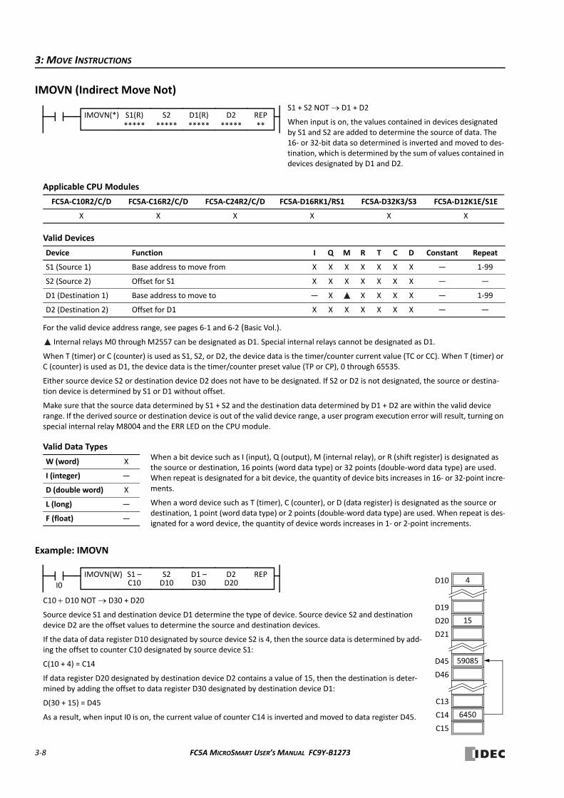
3: MOVE INSTRUCTIONS
IMOVN (Indirect Move Not)
Applicable CPU Modules
Valid Devices
For the valid device address range, see pages 6‐1 and 6‐2 (Basic Vol.).
Internal relays M0 through M2557 can be designated as D1. Special internal relays cannot be designated as D1.
When T (timer) or C (counter) is used as S1, S2, or D2, the device data is the timer/counter current value (TC or CC). When T (timer) or C (counter) is used as D1, the device data is the timer/counter preset value (TP or CP), 0 through 65535.
Either source device S2 or destination device D2 does not have to be designated. If S2 or D2 is not designated, the source or destina‐tion device is determined by S1 or D1 without offset.
Make sure that the source data determined by S1 + S2 and the destination data determined by D1 + D2 are within the valid device range. If the derived source or destination device is out of the valid device range, a user program execution error will result, turning on special internal relay M8004 and the ERR LED on the CPU module.
Valid Data Types
Example: IMOVN
FC5A‐C10R2/C/D FC5A‐C16R2/C/D FC5A‐C24R2/C/D FC5A‐D16RK1/RS1 FC5A‐D32K3/S3 FC5A‐D12K1E/S1E
X X X X X X
Device Function I Q M R T C D Constant Repeat
S1 (Source 1) Base address to move from X X X X X X X — 1‐99
S2 (Source 2) Offset for S1 X X X X X X X — —
D1 (Destination 1) Base address to move to — X X X X X — 1‐99
D2 (Destination 2) Offset for D1 X X X X X X X — —
W (word) X
I (integer) —
D (double word) X
L (long) —
F (float) —
S1 + S2 NOT D1 + D2
When input is on, the values contained in devices designated by S1 and S2 are added to determine the source of data. The 16‐ or 32‐bit data so determined is inverted and moved to des‐tination, which is determined by the sum of values contained in devices designated by D1 and D2.
REP**
S1(R)*****
D1(R)*****
IMOVN(*) S2*****
D2*****
When a bit device such as I (input), Q (output), M (internal relay), or R (shift register) is designated as the source or destination, 16 points (word data type) or 32 points (double‐word data type) are used. When repeat is designated for a bit device, the quantity of device bits increases in 16‐ or 32‐point incre‐ments.
When a word device such as T (timer), C (counter), or D (data register) is designated as the source or destination, 1 point (word data type) or 2 points (double‐word data type) are used. When repeat is des‐ignated for a word device, the quantity of device words increases in 1‐ or 2‐point increments.
C10 D10 NOT D30 + D20
Source device S1 and destination device D1 determine the type of device. Source device S2 and destination device D2 are the offset values to determine the source and destination devices.
If the data of data register D10 designated by source device S2 is 4, then the source data is determined by add‐ing the offset to counter C10 designated by source device S1:
C(10 + 4) = C14
If data register D20 designated by destination device D2 contains a value of 15, then the destination is deter‐mined by adding the offset to data register D30 designated by destination device D1:
D(30 + 15) = D45
As a result, when input I0 is on, the current value of counter C14 is inverted and moved to data register D45.
15D20
D19
D21
59085D45
4D10
C15
C13
D46
6450C14
I0
REPS1 –C10
D1 –D30
IMOVN(W) S2D10
D2D20
3‐8 FC5A MICROSMART USER’S MANUAL FC9Y‐B1273
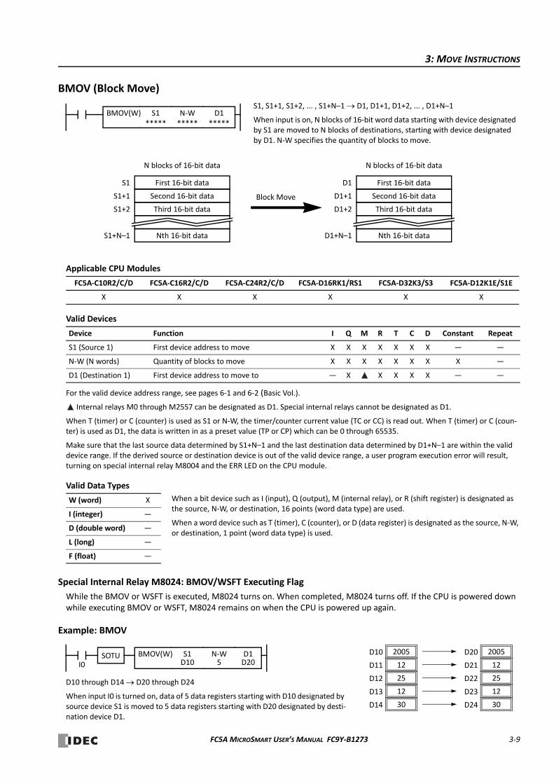
3: MOVE INSTRUCTIONS
BMOV (Block Move)
Applicable CPU Modules
Valid Devices
For the valid device address range, see pages 6‐1 and 6‐2 (Basic Vol.).
Internal relays M0 through M2557 can be designated as D1. Special internal relays cannot be designated as D1.
When T (timer) or C (counter) is used as S1 or N‐W, the timer/counter current value (TC or CC) is read out. When T (timer) or C (coun‐ter) is used as D1, the data is written in as a preset value (TP or CP) which can be 0 through 65535.
Make sure that the last source data determined by S1+N–1 and the last destination data determined by D1+N–1 are within the valid device range. If the derived source or destination device is out of the valid device range, a user program execution error will result, turning on special internal relay M8004 and the ERR LED on the CPU module.
Valid Data Types
Special Internal Relay M8024: BMOV/WSFT Executing Flag
While the BMOV or WSFT is executed, M8024 turns on. When completed, M8024 turns off. If the CPU is powered down while executing BMOV or WSFT, M8024 remains on when the CPU is powered up again.
Example: BMOV
FC5A‐C10R2/C/D FC5A‐C16R2/C/D FC5A‐C24R2/C/D FC5A‐D16RK1/RS1 FC5A‐D32K3/S3 FC5A‐D12K1E/S1E
X X X X X X
Device Function I Q M R T C D Constant Repeat
S1 (Source 1) First device address to move X X X X X X X — —
N‐W (N words) Quantity of blocks to move X X X X X X X X —
D1 (Destination 1) First device address to move to — X X X X X — —
W (word) X
I (integer) —
D (double word) —
L (long) —
F (float) —
S1, S1+1, S1+2, ... , S1+N–1 D1, D1+1, D1+2, ... , D1+N–1
When input is on, N blocks of 16‐bit word data starting with device designated by S1 are moved to N blocks of destinations, starting with device designated by D1. N‐W specifies the quantity of blocks to move.
BMOV(W) S1*****
D1*****
N‐W*****
First 16‐bit dataS1
Second 16‐bit dataS1+1
Third 16‐bit dataS1+2
Nth 16‐bit dataS1+N–1
N blocks of 16‐bit data
First 16‐bit dataD1
Second 16‐bit dataD1+1
Third 16‐bit dataD1+2
Nth 16‐bit dataD1+N–1
N blocks of 16‐bit data
Block Move
When a bit device such as I (input), Q (output), M (internal relay), or R (shift register) is designated as the source, N‐W, or destination, 16 points (word data type) are used.
When a word device such as T (timer), C (counter), or D (data register) is designated as the source, N‐W, or destination, 1 point (word data type) is used.
D1D20
D10 through D14 D20 through D24
When input I0 is turned on, data of 5 data registers starting with D10 designated by source device S1 is moved to 5 data registers starting with D20 designated by desti‐nation device D1.
12D11
2005D10
25D12
S1D10
N‐W5I0
BMOV(W)
12D13
30D14
12D21
2005D20
25D22
12D23
30D24
SOTU
FC5A MICROSMART USER’S MANUAL FC9Y‐B1273 3‐9
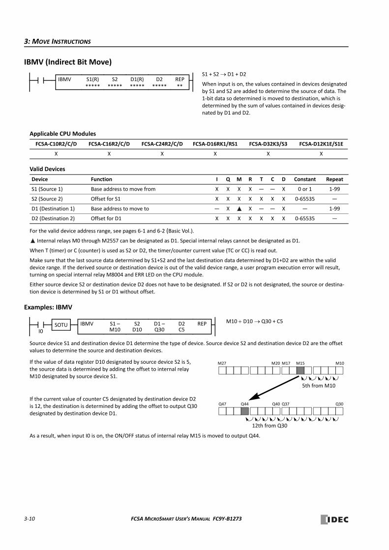
3: MOVE INSTRUCTIONS
IBMV (Indirect Bit Move)
Applicable CPU Modules
Valid Devices
For the valid device address range, see pages 6‐1 and 6‐2 (Basic Vol.).
Internal relays M0 through M2557 can be designated as D1. Special internal relays cannot be designated as D1.
When T (timer) or C (counter) is used as S2 or D2, the timer/counter current value (TC or CC) is read out.
Make sure that the last source data determined by S1+S2 and the last destination data determined by D1+D2 are within the valid device range. If the derived source or destination device is out of the valid device range, a user program execution error will result, turning on special internal relay M8004 and ERR LED on the CPU module.
Either source device S2 or destination device D2 does not have to be designated. If S2 or D2 is not designated, the source or destina‐tion device is determined by S1 or D1 without offset.
Examples: IBMV
Source device S1 and destination device D1 determine the type of device. Source device S2 and destination device D2 are the offset values to determine the source and destination devices.
As a result, when input I0 is on, the ON/OFF status of internal relay M15 is moved to output Q44.
FC5A‐C10R2/C/D FC5A‐C16R2/C/D FC5A‐C24R2/C/D FC5A‐D16RK1/RS1 FC5A‐D32K3/S3 FC5A‐D12K1E/S1E
X X X X X X
Device Function I Q M R T C D Constant Repeat
S1 (Source 1) Base address to move from X X X X — — X 0 or 1 1‐99
S2 (Source 2) Offset for S1 X X X X X X X 0‐65535 —
D1 (Destination 1) Base address to move to — X X — — X — 1‐99
D2 (Destination 2) Offset for D1 X X X X X X X 0‐65535 —
S1 + S2 D1 + D2
When input is on, the values contained in devices designated by S1 and S2 are added to determine the source of data. The 1‐bit data so determined is moved to destination, which is determined by the sum of values contained in devices desig‐nated by D1 and D2.
IBMV S1(R)*****
S2*****
D1(R)*****
D2*****
REP**
S1 –M10I0
IBMV S2D10
D1 –Q30
SOTU REPD2C5
M10 D10 Q30 + C5
M27 M10M17M20 M15
5th from M10
Q47 Q30Q37Q40
12th from Q30
Q44
If the value of data register D10 designated by source device S2 is 5, the source data is determined by adding the offset to internal relay M10 designated by source device S1.
If the current value of counter C5 designated by destination device D2 is 12, the destination is determined by adding the offset to output Q30 designated by destination device D1.
3‐10 FC5A MICROSMART USER’S MANUAL FC9Y‐B1273
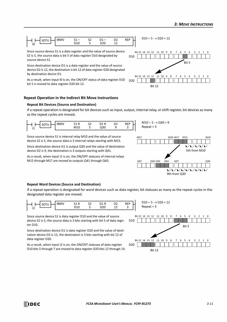
3: MOVE INSTRUCTIONS
Repeat Operation in the Indirect Bit Move Instructions
Repeat Bit Devices (Source and Destination)
If a repeat operation is designated for bit devices such as input, output, internal relay, or shift register, bit devices as many as the repeat cycles are moved.
Repeat Word Devices (Source and Destination)
If a repeat operation is designated for word devices such as data register, bit statuses as many as the repeat cycles in the designated data register are moved.
S1 –D10I0
IBMV S25
D1 –D20
SOTU REPD212
D10 5 D20 + 12
Bit 15
Bit 5
Bit 12
Since source device S1 is a data register and the value of source device S2 is 5, the source data is bit 5 of data register D10 designated by source device S1.
Since destination device D1 is a data register and the value of source device D2 is 12, the destination is bit 12 of data register D20 designated by destination device D1.
As a result, when input I0 is on, the ON/OFF status of data register D10 bit 5 is moved to data register D20 bit 12.
14 13 12 11 10 9 8 7 6 5 4 3 2 1 0
D10
Bit 15 14 13 12 11 10 9 8 7 6 5 4 3 2 1 0
D20
S1 RM10I1
IBMV S25
D1 RQ30
SOTU REP3
D29
M10 5 Q30 + 9Repeat = 3
M27 M10M17M20 M15
5th from M10
Q47 Q30Q37Q41
9th from Q30
Q44
Since source device S1 is internal relay M10 and the value of source device S2 is 5, the source data is 3 internal relays starting with M15.
Since destination device D1 is output Q30 and the value of destination device D2 is 9, the destination is 3 outputs starting with Q41.
As a result, when input I1 is on, the ON/OFF statuses of internal relays M15 through M17 are moved to outputs Q41 through Q43. Q43
S1 RD10I2
IBMV S25
D1 RD20
SOTU REP3
D212
D10 5 D20 + 12Repeat = 3
Since source device S1 is data register D10 and the value of source device S2 is 5, the source data is 3 bits starting with bit 5 of data regis‐ter D10.
Since destination device D1 is data register D20 and the value of desti‐nation device D2 is 12, the destination is 3 bits starting with bit 12 of data register D20.
As a result, when input I2 is on, the ON/OFF statuses of data register D10 bits 5 through 7 are moved to data register D20 bits 12 through 14.
Bit 15
Bit 5
Bit 12
14 13 12 11 10 9 8 7 6 5 4 3 2 1 0
D10
Bit 15 14 13 12 11 10 9 8 7 6 5 4 3 2 1 0
D20
FC5A MICROSMART USER’S MANUAL FC9Y‐B1273 3‐11
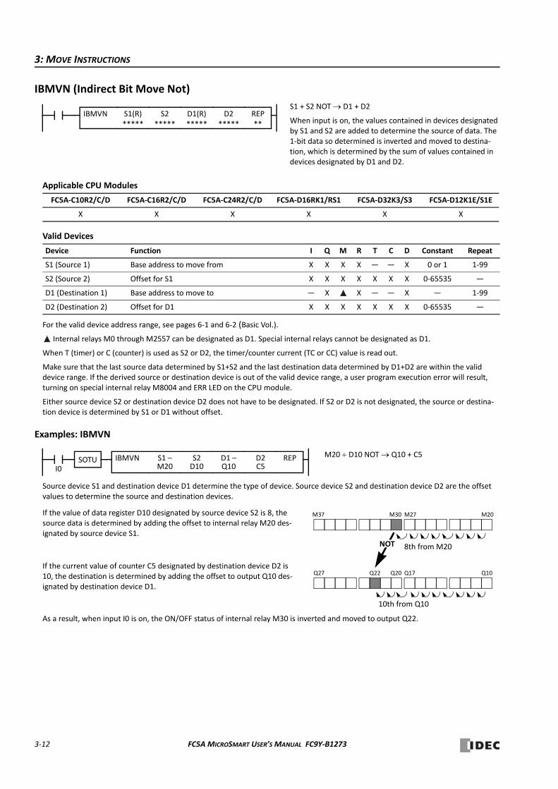
3: MOVE INSTRUCTIONS
IBMVN (Indirect Bit Move Not)
Applicable CPU Modules
Valid Devices
For the valid device address range, see pages 6‐1 and 6‐2 (Basic Vol.).
Internal relays M0 through M2557 can be designated as D1. Special internal relays cannot be designated as D1.
When T (timer) or C (counter) is used as S2 or D2, the timer/counter current (TC or CC) value is read out.
Make sure that the last source data determined by S1+S2 and the last destination data determined by D1+D2 are within the valid device range. If the derived source or destination device is out of the valid device range, a user program execution error will result, turning on special internal relay M8004 and ERR LED on the CPU module.
Either source device S2 or destination device D2 does not have to be designated. If S2 or D2 is not designated, the source or destina‐tion device is determined by S1 or D1 without offset.
Examples: IBMVN
Source device S1 and destination device D1 determine the type of device. Source device S2 and destination device D2 are the offset values to determine the source and destination devices.
As a result, when input I0 is on, the ON/OFF status of internal relay M30 is inverted and moved to output Q22.
FC5A‐C10R2/C/D FC5A‐C16R2/C/D FC5A‐C24R2/C/D FC5A‐D16RK1/RS1 FC5A‐D32K3/S3 FC5A‐D12K1E/S1E
X X X X X X
Device Function I Q M R T C D Constant Repeat
S1 (Source 1) Base address to move from X X X X — — X 0 or 1 1‐99
S2 (Source 2) Offset for S1 X X X X X X X 0‐65535 —
D1 (Destination 1) Base address to move to — X X — — X — 1‐99
D2 (Destination 2) Offset for D1 X X X X X X X 0‐65535 —
S1 + S2 NOT D1 + D2
When input is on, the values contained in devices designated by S1 and S2 are added to determine the source of data. The 1‐bit data so determined is inverted and moved to destina‐tion, which is determined by the sum of values contained in devices designated by D1 and D2.
IBMVN S1(R)*****
S2*****
D1(R)*****
REP**
D2*****
S1 –M20I0
IBMVN S2D10
SOTU D1 –Q10
REPD2C5
M20 D10 NOT Q10 + C5
M37 M20M27M30
8th from M20
Q27 Q10Q17Q20
10th from Q10
Q22
If the value of data register D10 designated by source device S2 is 8, the source data is determined by adding the offset to internal relay M20 des‐ignated by source device S1.
If the current value of counter C5 designated by destination device D2 is 10, the destination is determined by adding the offset to output Q10 des‐ignated by destination device D1.
NOT
3‐12 FC5A MICROSMART USER’S MANUAL FC9Y‐B1273
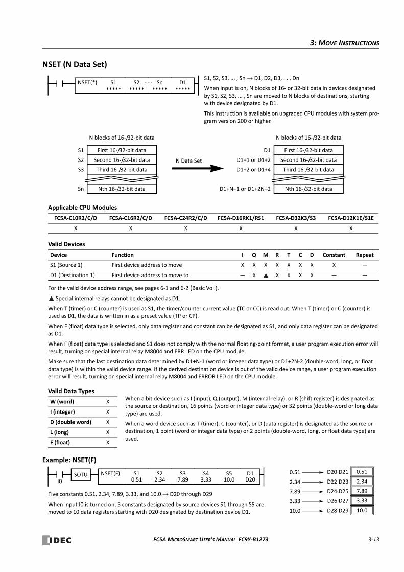
3: MOVE INSTRUCTIONS
NSET (N Data Set)
Applicable CPU Modules
Valid Devices
For the valid device address range, see pages 6‐1 and 6‐2 (Basic Vol.).
Special internal relays cannot be designated as D1.
When T (timer) or C (counter) is used as S1, the timer/counter current value (TC or CC) is read out. When T (timer) or C (counter) is used as D1, the data is written in as a preset value (TP or CP).
When F (float) data type is selected, only data register and constant can be designated as S1, and only data register can be designated as D1.
When F (float) data type is selected and S1 does not comply with the normal floating‐point format, a user program execution error will result, turning on special internal relay M8004 and ERR LED on the CPU module.
Make sure that the last destination data determined by D1+N‐1 (word or integer data type) or D1+2N‐2 (double‐word, long, or float data type) is within the valid device range. If the derived destination device is out of the valid device range, a user program execution error will result, turning on special internal relay M8004 and ERROR LED on the CPU module.
Valid Data Types
Example: NSET(F)
FC5A‐C10R2/C/D FC5A‐C16R2/C/D FC5A‐C24R2/C/D FC5A‐D16RK1/RS1 FC5A‐D32K3/S3 FC5A‐D12K1E/S1E
X X X X X X
Device Function I Q M R T C D Constant Repeat
S1 (Source 1) First device address to move X X X X X X X X —
D1 (Destination 1) First device address to move to — X X X X X — —
W (word) X
I (integer) X
D (double word) X
L (long) X
F (float) X
S1, S2, S3, ... , Sn D1, D2, D3, ... , Dn
When input is on, N blocks of 16‐ or 32‐bit data in devices designated by S1, S2, S3, ... , Sn are moved to N blocks of destinations, starting with device designated by D1.
This instruction is available on upgraded CPU modules with system pro‐gram version 200 or higher.
NSET(*)
S1*****
S2*****
Sn*****
..... D1*****
First 16‐/32‐bit dataS1
Second 16‐/32‐bit dataS2
Third 16‐/32‐bit dataS3
Nth 16‐/32‐bit dataSn
N blocks of 16‐/32‐bit data
First 16‐/32‐bit dataD1
Second 16‐/32‐bit dataD1+1 or D1+2
Third 16‐/32‐bit dataD1+2 or D1+4
Nth 16‐/32‐bit dataD1+N–1 or D1+2N–2
N blocks of 16‐/32‐bit data
N Data Set
When a bit device such as I (input), Q (output), M (internal relay), or R (shift register) is designated as the source or destination, 16 points (word or integer data type) or 32 points (double‐word or long data type) are used.
When a word device such as T (timer), C (counter), or D (data register) is designated as the source or destination, 1 point (word or integer data type) or 2 points (double‐word, long, or float data type) are used.
D1D20
Five constants 0.51, 2.34, 7.89, 3.33, and 10.0 D20 through D29
When input I0 is turned on, 5 constants designated by source devices S1 through S5 are moved to 10 data registers starting with D20 designated by destination device D1.
2.34
0.51
7.89
S10.51
S43.33I0
NSET(F)
3.33
10.0
2.34D22∙D23
0.51D20∙D21
7.89D24∙D25
3.33D26∙D27
10.0D28∙D29
S22.34
S37.89
S510.0
SOTU
FC5A MICROSMART USER’S MANUAL FC9Y‐B1273 3‐13
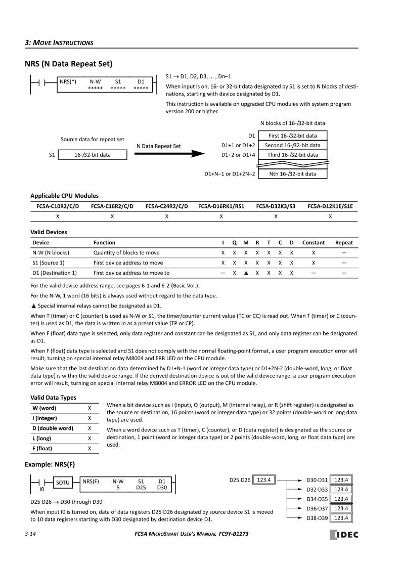
3: MOVE INSTRUCTIONS
NRS (N Data Repeat Set)
Applicable CPU Modules
Valid Devices
For the valid device address range, see pages 6‐1 and 6‐2 (Basic Vol.).
For the N‐W, 1 word (16 bits) is always used without regard to the data type.
Special internal relays cannot be designated as D1.
When T (timer) or C (counter) is used as N‐W or S1, the timer/counter current value (TC or CC) is read out. When T (timer) or C (coun‐ter) is used as D1, the data is written in as a preset value (TP or CP).
When F (float) data type is selected, only data register and constant can be designated as S1, and only data register can be designated as D1.
When F (float) data type is selected and S1 does not comply with the normal floating‐point format, a user program execution error will result, turning on special internal relay M8004 and ERR LED on the CPU module.
Make sure that the last destination data determined by D1+N‐1 (word or integer data type) or D1+2N‐2 (double‐word, long, or float data type) is within the valid device range. If the derived destination device is out of the valid device range, a user program execution error will result, turning on special internal relay M8004 and ERROR LED on the CPU module.
Valid Data Types
Example: NRS(F)
FC5A‐C10R2/C/D FC5A‐C16R2/C/D FC5A‐C24R2/C/D FC5A‐D16RK1/RS1 FC5A‐D32K3/S3 FC5A‐D12K1E/S1E
X X X X X X
Device Function I Q M R T C D Constant Repeat
N‐W (N blocks) Quantity of blocks to move X X X X X X X X —
S1 (Source 1) First device address to move X X X X X X X X —
D1 (Destination 1) First device address to move to — X X X X X — —
W (word) X
I (integer) X
D (double word) X
L (long) X
F (float) X
S1 D1, D2, D3, ... , Dn–1
When input is on, 16‐ or 32‐bit data designated by S1 is set to N blocks of desti‐nations, starting with device designated by D1.
This instruction is available on upgraded CPU modules with system program version 200 or higher.
NRS(*)
N‐W*****
S1*****
D1*****
16‐/32‐bit dataS1
Source data for repeat setFirst 16‐/32‐bit dataD1
Second 16‐/32‐bit dataD1+1 or D1+2
Third 16‐/32‐bit dataD1+2 or D1+4
Nth 16‐/32‐bit dataD1+N–1 or D1+2N–2
N blocks of 16‐/32‐bit data
N Data Repeat Set
When a bit device such as I (input), Q (output), M (internal relay), or R (shift register) is designated as the source or destination, 16 points (word or integer data type) or 32 points (double‐word or long data type) are used.
When a word device such as T (timer), C (counter), or D (data register) is designated as the source or destination, 1 point (word or integer data type) or 2 points (double‐word, long, or float data type) are used.
D1D30
D25∙D26 D30 through D39
When input I0 is turned on, data of data registers D25∙D26 designated by source device S1 is moved to 10 data registers starting with D30 designated by destination device D1.
N‐W5I0
NRS(F) 123.4D32∙D33
123.4D30∙D31
123.4D34∙D35
123.4D36∙D37
123.4D38∙D39
S1D25
123.4D25∙D26SOTU
3‐14 FC5A MICROSMART USER’S MANUAL FC9Y‐B1273

3: MOVE INSTRUCTIONS
XCHG (Exchange)
Applicable CPU Modules
Valid Devices
For the valid device address range, see pages 6‐1 and 6‐2 (Basic Vol.).
Internal relays M0 through M2557 can be designated as D1 or D2. Special internal relays cannot be designated as D1 or D2.
Valid Data Types
Examples: XCHG
• Data Type: Word
• Data Type: Double Word
FC5A‐C10R2/C/D FC5A‐C16R2/C/D FC5A‐C24R2/C/D FC5A‐D16RK1/RS1 FC5A‐D32K3/S3 FC5A‐D12K1E/S1E
X X X X X X
Device Function I Q M R T C D Constant Repeat
D1 (Destination 1) First device address to exchange — X s X — — X — —
D2 (Destination 2) First device address to exchange — X X — — X — —
W (word) X
I (integer) —
D (double word) X
L (long) —
F (float) —
Word data type: D1 D2Double‐word data type: D1∙D1+1 D2, D2+1
When input is on, the 16‐ or 32‐bit data in devices designated by D1 and D2 are exchanged with each other.
This instruction is available on upgraded CPU modules with system program version 210 or higher.
XCHG(*) D1*****
D2*****
When a bit device such as Q (output), M (internal relay), or R (shift register) is designated as the desti‐nation, 16 points (word data type) or 32 points (double‐word data type) are used.
When a word device such as D (data register) is designated as the destination, 1 point (word data type) or 2 points (double‐word data type) are used.
D21 D24
When input I0 is turned on, data of data registers D20 and D24 designated by devices D1 and D2 are exchanged with each other.
I0
XCHG(W) D2D24
D1D21
SOTU
D22
1000D21
D23
Before Exchange After Exchange
2000D24
D22
2000D21
D23
1000D24
Before Exchange After Exchange
D31∙D32 D37∙D38
When input I1 is turned on, data of data registers D31∙D32 and D37∙D38 designated by devices D1 and D2 are exchanged with each other.
I1
XCHG(D) D2D37
D1D31
SOTU 1234567890D31∙D32
D33∙D34
D35∙D36
9876543D31∙D32
D33∙D34
D35∙D36
9876543D37∙D38 1234567890D37∙D38
FC5A MICROSMART USER’S MANUAL FC9Y‐B1273 3‐15
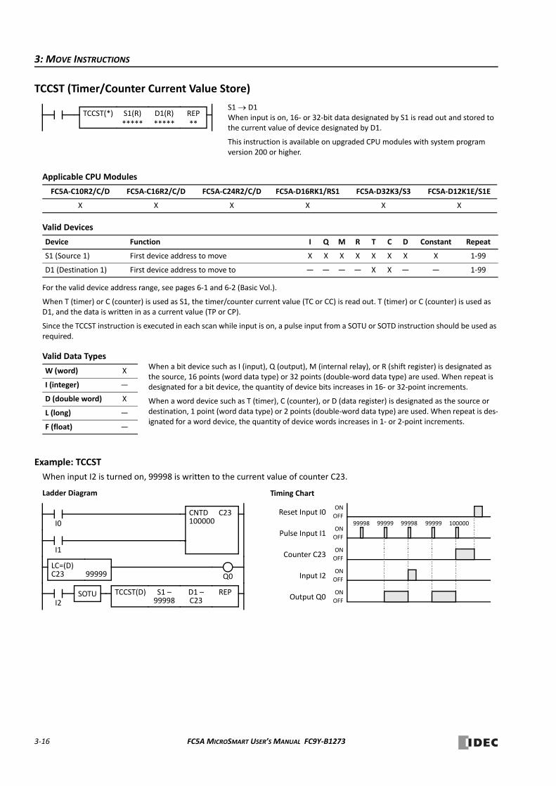
3: MOVE INSTRUCTIONS
TCCST (Timer/Counter Current Value Store)
Applicable CPU Modules
Valid Devices
For the valid device address range, see pages 6‐1 and 6‐2 (Basic Vol.).
When T (timer) or C (counter) is used as S1, the timer/counter current value (TC or CC) is read out. T (timer) or C (counter) is used as D1, and the data is written in as a current value (TP or CP).
Since the TCCST instruction is executed in each scan while input is on, a pulse input from a SOTU or SOTD instruction should be used as required.
Valid Data Types
Example: TCCST
When input I2 is turned on, 99998 is written to the current value of counter C23.
FC5A‐C10R2/C/D FC5A‐C16R2/C/D FC5A‐C24R2/C/D FC5A‐D16RK1/RS1 FC5A‐D32K3/S3 FC5A‐D12K1E/S1E
X X X X X X
Device Function I Q M R T C D Constant Repeat
S1 (Source 1) First device address to move X X X X X X X X 1‐99
D1 (Destination 1) First device address to move to — — — — X X — — 1‐99
W (word) X
I (integer) —
D (double word) X
L (long) —
F (float) —
S1 D1When input is on, 16‐ or 32‐bit data designated by S1 is read out and stored to the current value of device designated by D1.
This instruction is available on upgraded CPU modules with system program version 200 or higher.
REP**
S1(R)*****
D1(R)*****
TCCST(*)
When a bit device such as I (input), Q (output), M (internal relay), or R (shift register) is designated as the source, 16 points (word data type) or 32 points (double‐word data type) are used. When repeat is designated for a bit device, the quantity of device bits increases in 16‐ or 32‐point increments.
When a word device such as T (timer), C (counter), or D (data register) is designated as the source or destination, 1 point (word data type) or 2 points (double‐word data type) are used. When repeat is des‐ignated for a word device, the quantity of device words increases in 1‐ or 2‐point increments.
I2
REP
S1 –99998
D1 –C23
TCCST(D)
CNTD C23100000
I1
I0
Q0
SOTU
LC=(D)C23 99999
Reset Input I0ON
OFF
Pulse Input I1ON
OFF
Counter C23ON
OFF
Timing Chart
Output Q0ON
OFF
99998
Input I2
99999 99998
ON
OFF
Ladder Diagram
99999 100000
3‐16 FC5A MICROSMART USER’S MANUAL FC9Y‐B1273

4: DATA COMPARISON INSTRUCTIONS
IntroductionData can be compared using data comparison instructions, such as equal to, unequal to, less than, greater than, less than or equal to, and greater than or equal to. When the comparison result is true, an output or internal relay is turned on. The repeat operation can also be used to compare more than one set of data.
New logical OR operation option is added to the CMP instructions when the repeat operation is enabled. Repeated com‐parison results of CMP instructions can be selected from AND or OR operation, and the result is outputted to an output or internal relay. This option is available on upgraded CPU modules with system program version 200 or higher.
Three values can also be compared using the ICMP>= instruction.
Load comparison instructions have been added. The comparison result is loaded so that the following instructions can be initiated. These instructions are available on upgraded CPU modules with system program version 200 or higher.
Since the data comparison instructions are executed in each scan while input is on, a pulse input from a SOTU or SOTD instruction should be used as required.
CMP= (Compare Equal To)
CMP<> (Compare Unequal To)
CMP< (Compare Less Than)
CMP> (Compare Greater Than)
CMP<= (Compare Less Than or Equal To)
Data type W or I: S1 = S2 D1 onData type D, L, or F: S1∙S1+1 = S2∙S2+1 D1 onWhen input is on, 16‐ or 32‐bit data designated by source devices S1 and S2 are compared. When S1 data is equal to S2 data, destination device D1 is turned on. When the condition is not met, D1 is turned off.
REP**
S1(R)*****
D1(R)*****
CMP=(*)AND/OR
S2(R)*****
Data type W or I: S1 S2 D1 onData type D, L, or F: S1∙S1+1 S2∙S2+1 D1 onWhen input is on, 16‐ or 32‐bit data designated by source devices S1 and S2 are compared. When S1 data is not equal to S2 data, destina‐tion device D1 is turned on. When the condition is not met, D1 is turned off.
REP
**S1(R)*****
D1(R)*****
CMP<>(*)AND/OR
S2(R)*****
Data type W or I: S1 < S2 D1 onData type D, L, or F: S1∙S1+1 < S2∙S2+1 D1 onWhen input is on, 16‐ or 32‐bit data designated by source devices S1 and S2 are compared. When S1 data is less than S2 data, destination device D1 is turned on. When the condition is not met, D1 is turned off.
REP**
S1(R)*****
D1(R)*****
CMP<(*)AND/OR
S2(R)*****
Data type W or I: S1 > S2 D1 onData type D, L, or F: S1∙S1+1 > S2∙S2+1 D1 onWhen input is on, 16‐ or 32‐bit data designated by source devices S1 and S2 are compared. When S1 data is greater than S2 data, destina‐tion device D1 is turned on. When the condition is not met, D1 is turned off.
REP**
S1(R)*****
D1(R)*****
CMP>(*)AND/OR
S2(R)*****
Data type W or I: S1 S2 D1 onData type D, L, or F: S1∙S1+1 S2∙S2+1 D1 onWhen input is on, 16‐ or 32‐bit data designated by source devices S1 and S2 are compared. When S1 data is less than or equal to S2 data, destination device D1 is turned on. When the condition is not met, D1 is turned off.
REP
**S1(R)*****
D1(R)*****
CMP<=(*)AND/OR
S2(R)*****
FC5A MICROSMART USER’S MANUAL FC9Y‐B1273 4‐1
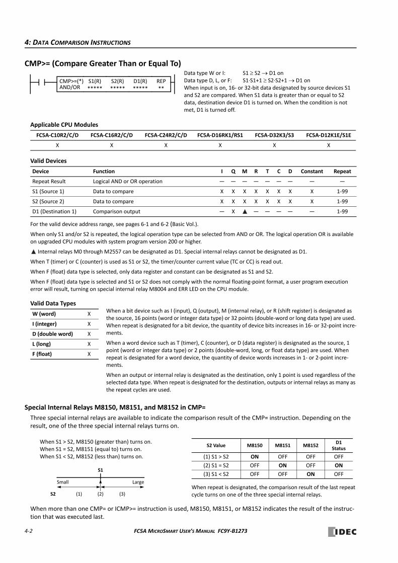
4: DATA COMPARISON INSTRUCTIONS
CMP>= (Compare Greater Than or Equal To)
Applicable CPU Modules
Valid Devices
For the valid device address range, see pages 6‐1 and 6‐2 (Basic Vol.).
When only S1 and/or S2 is repeated, the logical operation type can be selected from AND or OR. The logical operation OR is available on upgraded CPU modules with system program version 200 or higher.
Internal relays M0 through M2557 can be designated as D1. Special internal relays cannot be designated as D1.
When T (timer) or C (counter) is used as S1 or S2, the timer/counter current value (TC or CC) is read out.
When F (float) data type is selected, only data register and constant can be designated as S1 and S2.
When F (float) data type is selected and S1 or S2 does not comply with the normal floating‐point format, a user program execution error will result, turning on special internal relay M8004 and ERR LED on the CPU module.
Valid Data Types
Special Internal Relays M8150, M8151, and M8152 in CMP=
Three special internal relays are available to indicate the comparison result of the CMP= instruction. Depending on the result, one of the three special internal relays turns on.
When more than one CMP= or ICMP>= instruction is used, M8150, M8151, or M8152 indicates the result of the instruc‐tion that was executed last.
FC5A‐C10R2/C/D FC5A‐C16R2/C/D FC5A‐C24R2/C/D FC5A‐D16RK1/RS1 FC5A‐D32K3/S3 FC5A‐D12K1E/S1E
X X X X X X
Device Function I Q M R T C D Constant Repeat
Repeat Result Logical AND or OR operation — — — — — — — — —
S1 (Source 1) Data to compare X X X X X X X X 1‐99
S2 (Source 2) Data to compare X X X X X X X X 1‐99
D1 (Destination 1) Comparison output — X — — — — — 1‐99
W (word) X
I (integer) X
D (double word) X
L (long) X
F (float) X
Data type W or I: S1 S2 D1 onData type D, L, or F: S1∙S1+1 S2∙S2+1 D1 onWhen input is on, 16‐ or 32‐bit data designated by source devices S1 and S2 are compared. When S1 data is greater than or equal to S2 data, destination device D1 is turned on. When the condition is not met, D1 is turned off.
REP**
S1(R)*****
D1(R)*****
CMP>=(*)AND/OR
S2(R)*****
When a bit device such as I (input), Q (output), M (internal relay), or R (shift register) is designated as the source, 16 points (word or integer data type) or 32 points (double‐word or long data type) are used. When repeat is designated for a bit device, the quantity of device bits increases in 16‐ or 32‐point incre‐ments.
When a word device such as T (timer), C (counter), or D (data register) is designated as the source, 1 point (word or integer data type) or 2 points (double‐word, long, or float data type) are used. When repeat is designated for a word device, the quantity of device words increases in 1‐ or 2‐point incre‐ments.
When an output or internal relay is designated as the destination, only 1 point is used regardless of the selected data type. When repeat is designated for the destination, outputs or internal relays as many as the repeat cycles are used.
When S1 > S2, M8150 (greater than) turns on.When S1 = S2, M8151 (equal to) turns on.When S1 < S2, M8152 (less than) turns on.
S2 Value M8150 M8151 M8152 D1
Status
(1) S1 > S2 ON OFF OFF OFF
(2) S1 = S2 OFF ON OFF ON
(3) S1 < S2 OFF OFF ON OFF
S2
S1
(2)(1) (3)
Small LargeWhen repeat is designated, the comparison result of the last repeat cycle turns on one of the three special internal relays.
4‐2 FC5A MICROSMART USER’S MANUAL FC9Y‐B1273
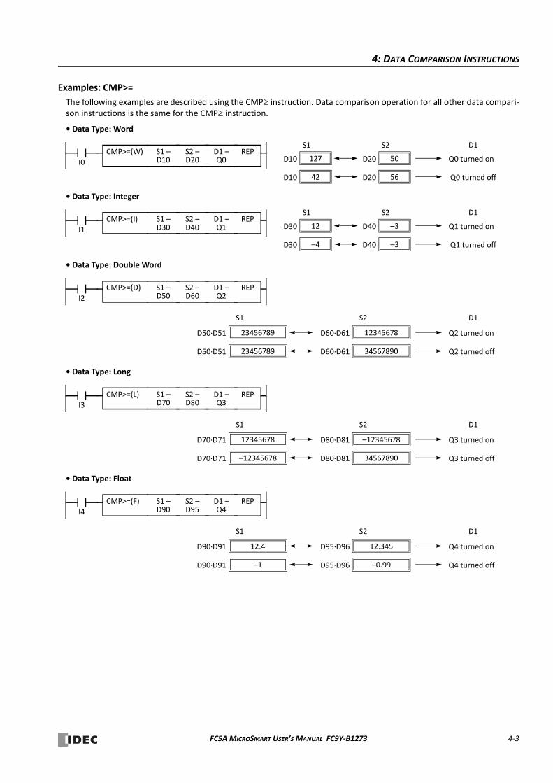
4: DATA COMPARISON INSTRUCTIONS
Examples: CMP>=
The following examples are described using the CMP instruction. Data comparison operation for all other data compari‐son instructions is the same for the CMP instruction.
• Data Type: Word
• Data Type: Integer
• Data Type: Double Word
• Data Type: Long
• Data Type: Float
I0
REPS1 –D10
D1 –Q0
CMP>=(W) S2 –D20
56D20
50D20
Q0 turned off
Q0 turned on
S2 D1
42D10
127D10
S1
I1
REPS1 –D30
D1 –Q1
CMP>=(I) S2 –D40
–3D40
–3D40
Q1 turned off
Q1 turned on
S2 D1
–4D30
12D30
S1
I2
REPS1 –D50
D1 –Q2
CMP>=(D) S2 –D60
S2 D1S1
23456789D50∙D51 12345678D60∙D61 Q2 turned on
23456789D50∙D51 34567890D60∙D61 Q2 turned off
I3
REPS1 –D70
D1 –Q3
CMP>=(L) S2 –D80
S2 D1S1
12345678D70∙D71 –12345678D80∙D81 Q3 turned on
–12345678D70∙D71 34567890D80∙D81 Q3 turned off
I4
REPS1 –D90
D1 –Q4
CMP>=(F) S2 –D95
S2 D1S1
12.4D90∙D91 12.345D95∙D96 Q4 turned on
–1D90∙D91 –0.99D95∙D96 Q4 turned off
FC5A MICROSMART USER’S MANUAL FC9Y‐B1273 4‐3

4: DATA COMPARISON INSTRUCTIONS
Repeat Operation in the Data Comparison Instructions
The following examples are described using the CMP instruction of the word and double word data types. Repeat oper‐ation for all other data comparison instructions and other data types is the same as the following examples.
New logical OR operation option is added to the CMP instructions when the repeat operation is enabled. Repeated com‐parison results of CMP instructions can be selected from AND or OR operation, and the result is outputted to an output or internal relay. This option is available on upgraded CPU modules with system program version 200 or higher.
Repeat One Source Device
When only S1 (source) is designated to repeat, source devices (as many as the repeat cycles, starting with the device des‐ignated by S1) are compared with the device designated by S2. The comparison results are ANDed or ORed and set to the destination device designated by D1.
• Data Type: Word (Repeat Logical Operation AND)
• Data Type: Word (Repeat Logical Operation OR)
• Data Type: Double Word (Repeat Logical Operation AND)
Repeat Two Source Devices
When S1 (source) and S2 (source) are designated to repeat, source devices (as many as the repeat cycles, starting with the devices designated by S1 and S2) are compared with each other. The comparison results are ANDed or ORed and set to the destination device designated by D1.
• Data Type: Word (Repeat Logical Operation AND)
• Data Type: Word (Repeat Logical Operation OR)
• Data Type: Double Word (Repeat Logical Operation AND)
I0
REP3
S1 RD10
D1 –M10
CMP>=(W)AND
S2 –15
AND15D11
10D10
20D12
M10
S1 (Repeat = 3) D1 (Repeat = 0)S2 (Repeat = 0)
15
15
15
I0
REP3
S1 RD10
D1 –M10
CMP>=(W)OR
S2 –15
OR15D11
10D10
20D12
M10
S1 (Repeat = 3) D1 (Repeat = 0)S2 (Repeat = 0)
15
15
15
I0
REP3
S1 RD20
D1 –M50
CMP>=(D)AND
S2 –D30
D22∙D23
D20∙D21
D24∙D25
AND
S1 (Repeat = 3) D1 (Repeat = 0)S2 (Repeat = 0)
D30∙D31
D30∙D31
D30∙D31
M50
AND M10I0
REP3
S1 RD10
D1 –M10
CMP>=(W)AND
S2 RD20
20D21
0D20
100D22
S2 (Repeat = 3) D1 (Repeat = 0)
20D11
10D10
30D12
S1 (Repeat = 3)
OR M10I0
REP3
S1 RD10
D1 –M10
CMP>=(W)OR
S2 RD20
20D21
0D20
100D22
S2 (Repeat = 3) D1 (Repeat = 0)
20D11
10D10
30D12
S1 (Repeat = 3)
D22∙D23
D20∙D21
D24∙D25
AND
S1 (Repeat = 3) D1 (Repeat = 0)S2 (Repeat = 3)
D30∙D31
D32∙D33
D34∙D35
M50I0
REP3
S1 RD20
D1 –M50
CMP>=(D)AND
S2 RD30
4‐4 FC5A MICROSMART USER’S MANUAL FC9Y‐B1273
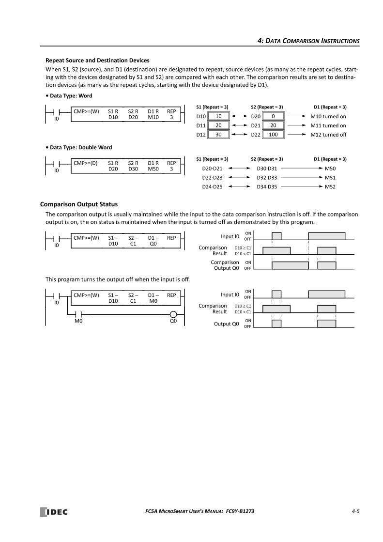
4: DATA COMPARISON INSTRUCTIONS
Repeat Source and Destination Devices
When S1, S2 (source), and D1 (destination) are designated to repeat, source devices (as many as the repeat cycles, start‐ing with the devices designated by S1 and S2) are compared with each other. The comparison results are set to destina‐tion devices (as many as the repeat cycles, starting with the device designated by D1).
• Data Type: Word
• Data Type: Double Word
Comparison Output Status
The comparison output is usually maintained while the input to the data comparison instruction is off. If the comparison output is on, the on status is maintained when the input is turned off as demonstrated by this program.
This program turns the output off when the input is off.
I0
REP3
S1 RD10
D1 RM10
CMP>=(W) S2 RD20
20D21
0D20
100D22
M11 turned on
M10 turned on
M12 turned off
S2 (Repeat = 3) D1 (Repeat = 3)
20D11
10D10
30D12
S1 (Repeat = 3)
D22∙D23
D20∙D21
D24∙D25
S1 (Repeat = 3) D1 (Repeat = 3)S2 (Repeat = 3)
D30∙D31
D32∙D33
D34∙D35
M51
M50
M52
I0
REP3
S1 RD20
D1 RM50
CMP>=(D) S2 RD30
Input I0ON
OFF
Comparison D10 C1D10 < C1
Comparison ON
OFF
I0
REPS1 –D10
D1 –Q0
CMP>=(W)
Result
Output Q0
S2 –C1
I0
M0
REPS1 –D10
D1 –M0
S2 –C1
Input I0ON
OFF
Comparison D10 C1D10 < C1
ON
OFF
Result
Output Q0
CMP>=(W)
Q0
FC5A MICROSMART USER’S MANUAL FC9Y‐B1273 4‐5
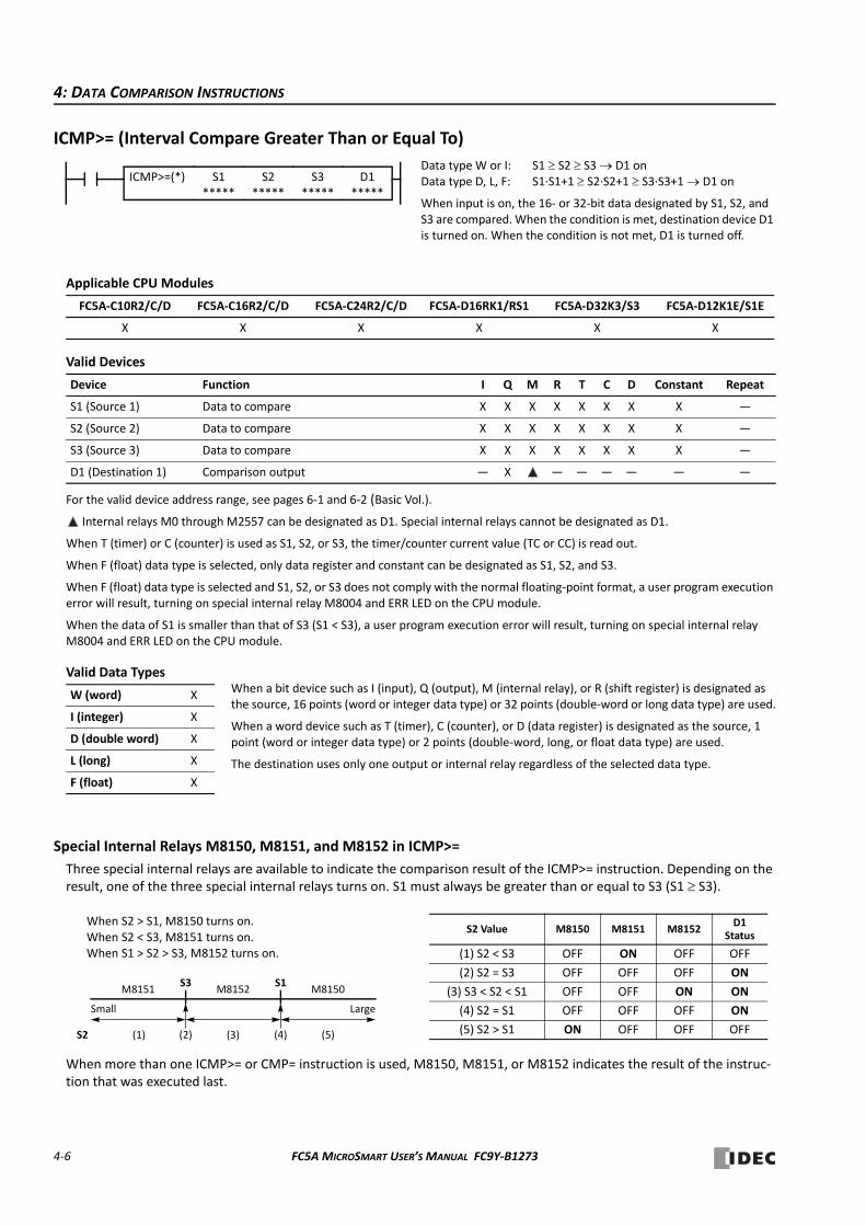
4: DATA COMPARISON INSTRUCTIONS
ICMP>= (Interval Compare Greater Than or Equal To)
Applicable CPU Modules
Valid Devices
For the valid device address range, see pages 6‐1 and 6‐2 (Basic Vol.).
Internal relays M0 through M2557 can be designated as D1. Special internal relays cannot be designated as D1.
When T (timer) or C (counter) is used as S1, S2, or S3, the timer/counter current value (TC or CC) is read out.
When F (float) data type is selected, only data register and constant can be designated as S1, S2, and S3.
When F (float) data type is selected and S1, S2, or S3 does not comply with the normal floating‐point format, a user program execution error will result, turning on special internal relay M8004 and ERR LED on the CPU module.
When the data of S1 is smaller than that of S3 (S1 < S3), a user program execution error will result, turning on special internal relay M8004 and ERR LED on the CPU module.
Valid Data Types
Special Internal Relays M8150, M8151, and M8152 in ICMP>=
Three special internal relays are available to indicate the comparison result of the ICMP>= instruction. Depending on the result, one of the three special internal relays turns on. S1 must always be greater than or equal to S3 (S1 S3).
When more than one ICMP>= or CMP= instruction is used, M8150, M8151, or M8152 indicates the result of the instruc‐tion that was executed last.
FC5A‐C10R2/C/D FC5A‐C16R2/C/D FC5A‐C24R2/C/D FC5A‐D16RK1/RS1 FC5A‐D32K3/S3 FC5A‐D12K1E/S1E
X X X X X X
Device Function I Q M R T C D Constant Repeat
S1 (Source 1) Data to compare X X X X X X X X —
S2 (Source 2) Data to compare X X X X X X X X —
S3 (Source 3) Data to compare X X X X X X X X —
D1 (Destination 1) Comparison output — X — — — — — —
W (word) X
I (integer) X
D (double word) X
L (long) X
F (float) X
Data type W or I: S1 S2 S3 D1 onData type D, L, F: S1∙S1+1 S2∙S2+1 S3∙S3+1 D1 on
When input is on, the 16‐ or 32‐bit data designated by S1, S2, and S3 are compared. When the condition is met, destination device D1 is turned on. When the condition is not met, D1 is turned off.
ICMP>=(*) S1*****
S2*****
S3*****
D1*****
When a bit device such as I (input), Q (output), M (internal relay), or R (shift register) is designated as the source, 16 points (word or integer data type) or 32 points (double‐word or long data type) are used.
When a word device such as T (timer), C (counter), or D (data register) is designated as the source, 1 point (word or integer data type) or 2 points (double‐word, long, or float data type) are used.
The destination uses only one output or internal relay regardless of the selected data type.
When S2 > S1, M8150 turns on.When S2 < S3, M8151 turns on.When S1 > S2 > S3, M8152 turns on.
S2 Value M8150 M8151 M8152 D1
Status
(1) S2 < S3 OFF ON OFF OFF
(2) S2 = S3 OFF OFF OFF ON
(3) S3 < S2 < S1 OFF OFF ON ON
(4) S2 = S1 OFF OFF OFF ON
(5) S2 > S1 ON OFF OFF OFFS2
S3 S1M8151 M8152 M8150
(2)(1) (3) (5)(4)
Small Large
4‐6 FC5A MICROSMART USER’S MANUAL FC9Y‐B1273
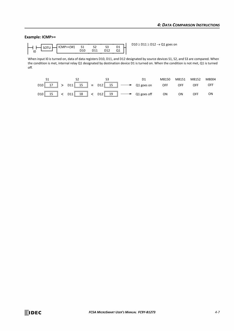
4: DATA COMPARISON INSTRUCTIONS
Example: ICMP>=
D1Q1
When input I0 is turned on, data of data registers D10, D11, and D12 designated by source devices S1, S2, and S3 are compared. When the condition is met, internal relay Q1 designated by destination device D1 is turned on. When the condition is not met, Q1 is turned off.
S1D10I0
ICMP>=(W) S2D11
S3D12
SOTUD10 D11 D12 Q1 goes on
15D11
S2
17D10
S1
15D12
S3
> = Q1 goes on
D1 M8151 M8152 M8004M8150
OFF OFF OFF OFF
18D1115D10 19D12< < Q1 goes off ON ON OFF ON
FC5A MICROSMART USER’S MANUAL FC9Y‐B1273 4‐7
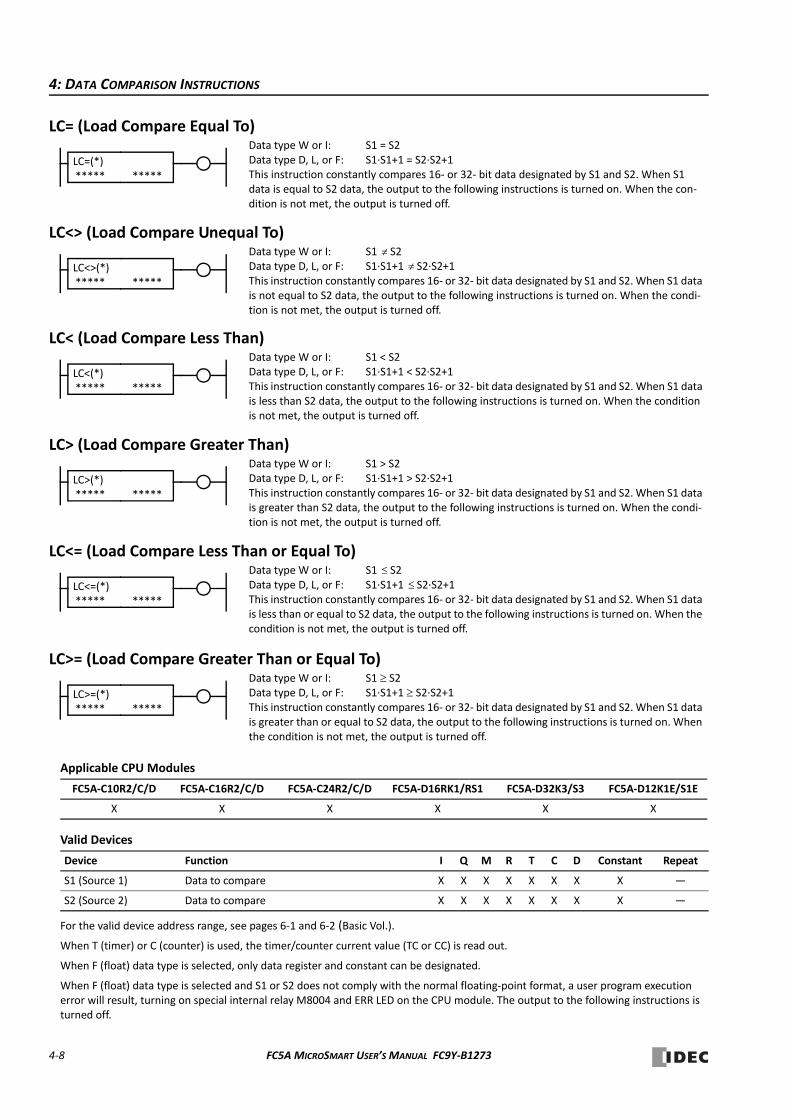
4: DATA COMPARISON INSTRUCTIONS
LC= (Load Compare Equal To)
LC<> (Load Compare Unequal To)
LC< (Load Compare Less Than)
LC> (Load Compare Greater Than)
LC<= (Load Compare Less Than or Equal To)
LC>= (Load Compare Greater Than or Equal To)
Applicable CPU Modules
Valid Devices
For the valid device address range, see pages 6‐1 and 6‐2 (Basic Vol.).
When T (timer) or C (counter) is used, the timer/counter current value (TC or CC) is read out.
When F (float) data type is selected, only data register and constant can be designated.
When F (float) data type is selected and S1 or S2 does not comply with the normal floating‐point format, a user program execution error will result, turning on special internal relay M8004 and ERR LED on the CPU module. The output to the following instructions is turned off.
FC5A‐C10R2/C/D FC5A‐C16R2/C/D FC5A‐C24R2/C/D FC5A‐D16RK1/RS1 FC5A‐D32K3/S3 FC5A‐D12K1E/S1E
X X X X X X
Device Function I Q M R T C D Constant Repeat
S1 (Source 1) Data to compare X X X X X X X X —
S2 (Source 2) Data to compare X X X X X X X X —
Data type W or I: S1 = S2Data type D, L, or F: S1∙S1+1 = S2∙S2+1This instruction constantly compares 16‐ or 32‐ bit data designated by S1 and S2. When S1 data is equal to S2 data, the output to the following instructions is turned on. When the con‐dition is not met, the output is turned off.
LC=(*)*****
*****
Data type W or I: S1 S2Data type D, L, or F: S1∙S1+1 S2∙S2+1This instruction constantly compares 16‐ or 32‐ bit data designated by S1 and S2. When S1 data is not equal to S2 data, the output to the following instructions is turned on. When the condi‐tion is not met, the output is turned off.
LC<>(*)
*****
*****
Data type W or I: S1 < S2Data type D, L, or F: S1∙S1+1 < S2∙S2+1This instruction constantly compares 16‐ or 32‐ bit data designated by S1 and S2. When S1 data is less than S2 data, the output to the following instructions is turned on. When the condition is not met, the output is turned off.
LC<(*)*****
*****
Data type W or I: S1 > S2Data type D, L, or F: S1∙S1+1 > S2∙S2+1This instruction constantly compares 16‐ or 32‐ bit data designated by S1 and S2. When S1 data is greater than S2 data, the output to the following instructions is turned on. When the condi‐tion is not met, the output is turned off.
LC>(*)*****
*****
Data type W or I: S1 S2Data type D, L, or F: S1∙S1+1 S2∙S2+1This instruction constantly compares 16‐ or 32‐ bit data designated by S1 and S2. When S1 data is less than or equal to S2 data, the output to the following instructions is turned on. When the condition is not met, the output is turned off.
LC<=(*)
*****
*****
Data type W or I: S1 S2Data type D, L, or F: S1∙S1+1 S2∙S2+1This instruction constantly compares 16‐ or 32‐ bit data designated by S1 and S2. When S1 data is greater than or equal to S2 data, the output to the following instructions is turned on. When the condition is not met, the output is turned off.
LC>=(*)*****
*****
4‐8 FC5A MICROSMART USER’S MANUAL FC9Y‐B1273
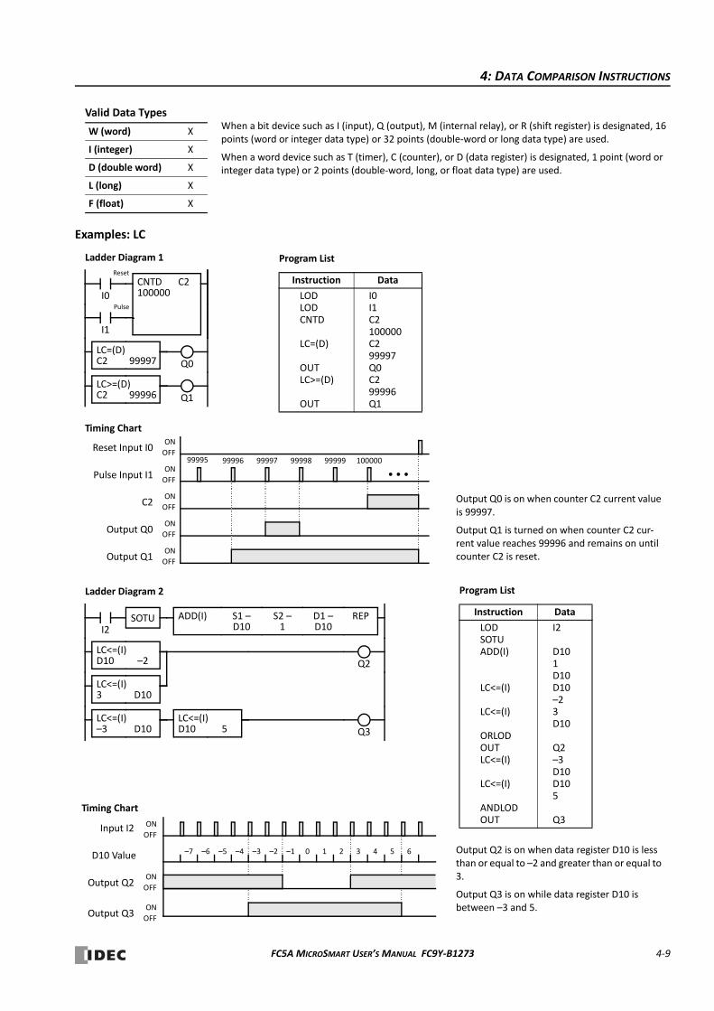
4: DATA COMPARISON INSTRUCTIONS
Valid Data Types
Examples: LC
W (word) X
I (integer) X
D (double word) X
L (long) X
F (float) X
When a bit device such as I (input), Q (output), M (internal relay), or R (shift register) is designated, 16 points (word or integer data type) or 32 points (double‐word or long data type) are used.
When a word device such as T (timer), C (counter), or D (data register) is designated, 1 point (word or integer data type) or 2 points (double‐word, long, or float data type) are used.
Ladder Diagram 1
Timing Chart
LC=(D)C2 99997
CNTD C2100000
I1
Reset
Pulse
I0
LC>=(D)C2 99996
Reset Input I0ON
OFF
Pulse Input I1ON
OFF
C2ON
OFF
Output Q1ON
OFF
Output Q0
• • •
99996 99997 99998
ON
OFF
99999 100000
Instruction Data
LODLODCNTD
LC=(D)
OUTLC>=(D)
OUT
I0I1C2100000C299997Q0C299996Q1
Program List
Output Q0 is on when counter C2 current value is 99997.
Output Q1 is turned on when counter C2 cur‐rent value reaches 99996 and remains on until counter C2 is reset.
Q0
Q1
99995
Ladder Diagram 2
LC<=(I)D10 –2
I2
Instruction Data
LODSOTUADD(I)
LC<=(I)
LC<=(I)
ORLODOUTLC<=(I)
LC<=(I)
ANDLODOUT
I2
D101D10D10–23D10
Q2–3D10D105
Q3
Program List
Output Q2 is on when data register D10 is less than or equal to –2 and greater than or equal to 3.
Output Q3 is on while data register D10 is between –3 and 5.
Q2
REPS1 –D10
S2 –1
ADD(I) D1 –D10
SOTU
Timing Chart
Input I2 ON
OFF
D10 Value
Output Q3ON
OFF
Output Q2ON
OFF
–7 –6 –3 –2 –1 2 3 4–5 –4 0 1 5 6
LC<=(I)3 D10
LC<=(I)–3 D10
LC<=(I)D10 5 Q3
FC5A MICROSMART USER’S MANUAL FC9Y‐B1273 4‐9

4: DATA COMPARISON INSTRUCTIONS
4‐10 FC5A MICROSMART USER’S MANUAL FC9Y‐B1273
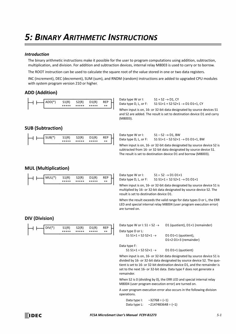
5: BINARY ARITHMETIC INSTRUCTIONS
IntroductionThe binary arithmetic instructions make it possible for the user to program computations using addition, subtraction, multiplication, and division. For addition and subtraction devices, internal relay M8003 is used to carry or to borrow.
The ROOT instruction can be used to calculate the square root of the value stored in one or two data registers.
INC (increment), DEC (decrement), SUM (sum), and RNDM (random) instructions are added to upgraded CPU modules with system program version 210 or higher.
ADD (Addition)
SUB (Subtraction)
MUL (Multiplication)
DIV (Division)
Data type W or I: S1 + S2 D1, CY Data type D, L, or F: S1∙S1+1 + S2∙S2+1 D1∙D1+1, CY
When input is on, 16‐ or 32‐bit data designated by source devices S1 and S2 are added. The result is set to destination device D1 and carry (M8003).
REP**
S1(R)*****
D1(R)*****
ADD(*) S2(R)*****
Data type W or I: S1 – S2 D1, BW Data type D, L, or F: S1∙S1+1 – S2∙S2+1 D1∙D1+1, BW
When input is on, 16‐ or 32‐bit data designated by source device S2 is subtracted from 16‐ or 32‐bit data designated by source device S1. The result is set to destination device D1 and borrow (M8003).
REP**
S1(R)*****
D1(R)*****
SUB(*) S2(R)*****
Data type W or I: S1 S2 D1∙D1+1Data type D, L, or F: S1∙S1+1 S2∙S2+1 D1∙D1+1
When input is on, 16‐ or 32‐bit data designated by source device S1 is multiplied by 16‐ or 32‐bit data designated by source device S2. The result is set to destination device D1.
When the result exceeds the valid range for data types D or L, the ERR LED and special internal relay M8004 (user program execution error) are turned on.
REP**
S1(R)*****
D1(R)*****
MUL(*) S2(R)*****
Data type W or I: S1 ÷ S2 D1 (quotient), D1+1 (remainder)
Data type D or L:S1∙S1+1 ÷ S2∙S2+1 D1∙D1+1 (quotient),
D1+2∙D1+3 (remainder)
Data type F:S1∙S1+1 ÷ S2∙S2+1 D1∙D1+1 (quotient)
When input is on, 16‐ or 32‐bit data designated by source device S1 is divided by 16‐ or 32‐bit data designated by source device S2. The quo‐tient is set to 16‐ or 32‐bit destination device D1, and the remainder is set to the next 16‐ or 32‐bit data. Data type F does not generate a remainder.
When S2 is 0 (dividing by 0), the ERR LED and special internal relay M8004 (user program execution error) are turned on.
A user program execution error also occurs in the following division operations.
Data type I: –32768 ÷ (–1)Data type L: –2147483648 ÷ (–1)
REP**
S1(R)*****
D1(R)*****
DIV(*) S2(R)*****
FC5A MicroSmart User’s Manual FC9Y‐B1273 5‐1

5: Binary Arithmetic Instructions
Applicable CPU Modules
Valid Devices
For the valid device address range, see pages 6‐1 and 6‐2 (Basic Vol.).
Internal relays M0 through M2557 can be designated as D1. Special internal relays cannot be designated as D1.
When T (timer) or C (counter) is used as S1 or S2, the timer/counter current value (TC or CC) is read out. When T (timer) or C (counter) is used as D1, the data is written in as a preset value (TP or CP) which can be 0 through 65535.
When F (float) data type is selected, only data register and constant can be designated as S1 and S2.
When F (float) data type is selected and S1 or S2 does not comply with the normal floating‐point format, a user program execution error will result, turning on special internal relay M8004 and ERR LED on the CPU module.
Since the binary arithmetic instructions are executed in each scan while input is on, a pulse input from a SOTU or SOTD instruction should be used as required.
Valid Data Types
Using Carry or Borrow Signals
When the D1 (destination) data is out of the valid data range as a result of any binary arithmetic operation, a carry or bor‐row occurs, and special internal relay M8003 is turned on.
FC5A‐C10R2/C/D FC5A‐C16R2/C/D FC5A‐C24R2/C/D FC5A‐D16RK1/RS1 FC5A‐D32K3/S3 FC5A‐D12K1E/S1E
X X X X X X
Device Function I Q M R T C D Constant Repeat
S1 (Source 1) Data for calculation X X X X X X X X 1‐99
S2 (Source 2) Data for calculation X X X X X X X X 1‐99
D1 (Destination 1) Destination to store results — X X X X X — 1‐99
W (word) X
I (integer) X
D (double word) X
L (long) X
F (float) X
Data Type Carry/borrow occurs when D1 is out of the range between
W (word) 0 and 65,535
I (integer) –32,768 and 32,767
D (double word) 0 and 4,294,967,295
L (long) –2,147,483,648 and 2,147,483,647
F (float)–3.4028231038 and –1.17549510–38
1.17549510–38 and 3.4028231038
When a bit device such as I (input), Q (output), M (internal relay), or R (shift register) is designated as the source, 16 points (word or integer data type) or 32 points (double‐word, long, or float data type) are used. When repeat is designated for a bit device, the quantity of device bits increases in 16‐ or 32‐point increments.
When a word device such as T (timer), C (counter), or D (data register) is designated as the source, 1 point (word or integer data type) or 2 points (double‐word, long, or float data type) are used. When repeat is designated for a word device, the quantity of device words increases in 1‐ or 2‐point incre‐ments.
5‐2 FC5A MicroSmart User’s Manual FC9Y‐B1273
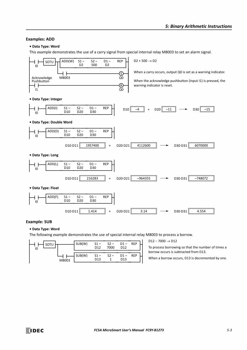
5: Binary Arithmetic Instructions
Examples: ADD
• Data Type: Word
This example demonstrates the use of a carry signal from special internal relay M8003 to set an alarm signal.
• Data Type: Integer
• Data Type: Double Word
• Data Type: Long
• Data Type: Float
Example: SUB
• Data Type: Word
The following example demonstrates the use of special internal relay M8003 to process a borrow.
I0
REPS2 –500
D1 –D2
SOTU
M8003
I1
D2 + 500 D2
When a carry occurs, output Q0 is set as a warning indicator.
When the acknowledge pushbutton (input I1) is pressed, the warning indicator is reset.
AcknowledgePushbutton
S1 –D2
ADD(W)
Q0S
Q0R
I0
REPS2 –D20
D1 –D30
S1 –D10
ADD(I) –4D10 + –15D30–11D20
I0
REPS2 –D20
D1 –D30
S1 –D10
ADD(D)
+1957400D10∙D11 4112600D20∙D21 6070000D30∙D31
I0
REPS2 –D20
D1 –D30
S1 –D10
ADD(L)
+216283D10∙D11 –964355D20∙D21 –748072D30∙D31
I0
REPS2 –D20
D1 –D30
S1 –D10
ADD(F)
+1.414D10∙D11 3.14D20∙D21 4.554D30∙D31
I0SOTU
M8003
D12 – 7000 D12
To process borrowing so that the number of times a borrow occurs is subtracted from D13.
When a borrow occurs, D13 is decremented by one.
REPS2 –7000
D1 –D12
S1 –D12
SUB(W)
REPS2 –1
D1 –D13
S1 –D13
SUB(W)
FC5A MicroSmart User’s Manual FC9Y‐B1273 5‐3
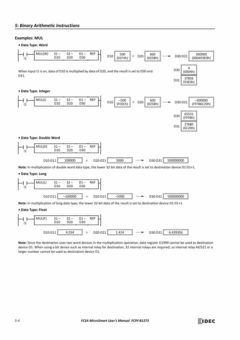
5: Binary Arithmetic Instructions
Examples: MUL
• Data Type: Word
• Data Type: Integer
• Data Type: Double Word
Note: In multiplication of double word data type, the lower 32‐bit data of the result is set to destination device D1∙D1+1.
• Data Type: Long
Note: In multiplication of long data type, the lower 32‐bit data of the result is set to destination device D1∙D1+1.
• Data Type: Float
Note: Since the destination uses two word devices in the multiplication operation, data register D1999 cannot be used as destination device D1. When using a bit device such as internal relay for destination, 32 internal relays are required; so internal relay M2521 or a larger number cannot be used as destination device D1.
I1
REPS2 –D20
D1 –D30
S1 –D10
MUL(W)D10 300000
(000493E0h)500
(01F4h)600
(0258h)D20 D30∙D31
When input I1 is on, data of D10 is multiplied by data of D20, and the result is set to D30 and D31.
D3137856(93E0h)
D304
(0004h)
I1
REPS2 –D20
D1 –D30
S1 –D10
MUL(I)D10 –300000
(FFFB6C20h)–500
(FE0Ch)600
(0258h)D20 D30∙D31
D3127680(6C20h)
D3065531(FFFBh)
I1
REPS2 –D20
D1 –D30
S1 –D10
MUL(D)
100000D10∙D11 5000D20∙D21 500000000D30∙D31
I1
REPS2 –D20
D1 –D30
S1 –D10
MUL(L)
–100000D10∙D11 –5000D20∙D21 500000000D30∙D31
I1
REPS2 –D20
D1 –D30
S1 –D10
MUL(F)
4.554D10∙D11 1.414D20∙D21 6.439356D30∙D31
5‐4 FC5A MicroSmart User’s Manual FC9Y‐B1273

5: Binary Arithmetic Instructions
Examples: DIV
• Data Type: Word
Note: Since the destination uses two word devices in the division operation of word data type, data register D1999 cannot be used as destination device D1. When using a bit device such as internal relay for destination, 32 internal relays are required; so M2521 or a larger number cannot be used as destination device D1.
• Data Type: Integer
Note: Since the destination uses two word devices in the division operation of integer data type, data register D1999 cannot be used as destination device D1. When using a bit device such as internal relay for destination, 32 internal relays are required; so M2521 or a larger number cannot be used as destination device D1.
• Data Type: Double Word
Note: Since the destination uses four word devices in the division operation of double‐word data type, data registers D1997 through D1999 cannot be used as destination device D1. When using a bit device such as internal relay for destination, 64 internal relays are required; so M2481 or a larger number cannot be used as destination device D1.
• Data Type: Long
Note: Since the destination uses four word devices in the division operation of long data type, data registers D1997 through D1999 cannot be used as destination device D1. When using a bit device such as internal relay for destination, 64 internal relays are required; so M2481 or a larger number cannot be used as destination device D1.
• Data Type: Float
Note: Since the destination uses two word devices in the division operation of float data type, data register D1999 cannot be used as destination device D1.
When input I2 is on, data of D10 is divided by data of D20. The quotient is set to D30, and the remainder is set to D31.
I2
REPS2 –D20
D1 –D30
S1 –D10
DIV(W)Quotient Remainder
50D10 ÷ 7D307D20 1D31
I2
REPS2 –D20
D1 –D30
S1 –D10
DIV(I)Quotient Remainder
50D10 ÷ –7D30–7D20 1D31
I1
REPS2 –D20
D1 –D30
S1 –D10
DIV(D)
÷100000D10∙D11 70000D20∙D21 1D30∙D31 30000D32∙D33
Quotient Remainder
I1
REPS2 –D20
D1 –D30
S1 –D10
DIV(L)
÷100000D10∙D11 –70000D20∙D21 –1D30∙D31 30000D32∙D33
Quotient Remainder
I1
REPS2 –D20
D1 –D30
S1 –D10
DIV(F)
÷4.43996D10∙D11 3.14D20∙D21 1.414D30∙D31
Quotient
FC5A MicroSmart User’s Manual FC9Y‐B1273 5‐5
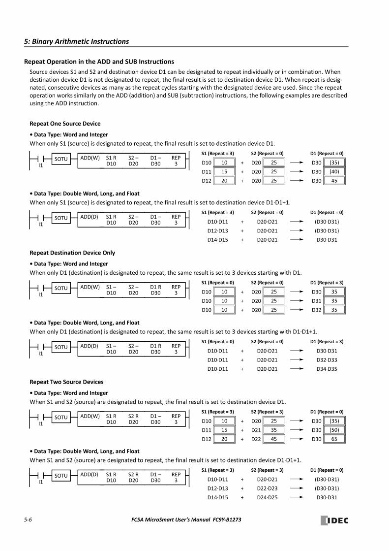
5: Binary Arithmetic Instructions
Repeat Operation in the ADD and SUB Instructions
Source devices S1 and S2 and destination device D1 can be designated to repeat individually or in combination. When destination device D1 is not designated to repeat, the final result is set to destination device D1. When repeat is desig‐nated, consecutive devices as many as the repeat cycles starting with the designated device are used. Since the repeat operation works similarly on the ADD (addition) and SUB (subtraction) instructions, the following examples are described using the ADD instruction.
Repeat One Source Device
• Data Type: Word and Integer
When only S1 (source) is designated to repeat, the final result is set to destination device D1.
• Data Type: Double Word, Long, and Float
When only S1 (source) is designated to repeat, the final result is set to destination device D1∙D1+1.
Repeat Destination Device Only
• Data Type: Word and Integer
When only D1 (destination) is designated to repeat, the same result is set to 3 devices starting with D1.
• Data Type: Double Word, Long, and Float
When only D1 (destination) is designated to repeat, the same result is set to 3 devices starting with D1∙D1+1.
Repeat Two Source Devices
• Data Type: Word and Integer
When S1 and S2 (source) are designated to repeat, the final result is set to destination device D1.
• Data Type: Double Word, Long, and Float
When S1 and S2 (source) are designated to repeat, the final result is set to destination device D1∙D1+1.
I1
REP3
S1 RD10
D1 –D30
15D11
10D10
20D12
S1 (Repeat = 3) D1 (Repeat = 0)S2 –D20
S2 (Repeat = 0)
+
+
+
(40)D30
(35)D30
45D30
25D20
25D20
25D20
SOTU ADD(W)
I1
REP3
S1 RD10
D1 –D30
D12∙D13
D10∙D11
D14∙D15
S1 (Repeat = 3) D1 (Repeat = 0)S2 –D20
S2 (Repeat = 0)
+
+
+
(D30∙D31)
(D30∙D31)
D30∙D31
D20∙D21
D20∙D21
D20∙D21
SOTU ADD(D)
I1
REP3
S1 –D10
D1 RD30
10D10
10D10
10D10
S1 (Repeat = 0) D1 (Repeat = 3)S2 –D20
S2 (Repeat = 0)
+
+
+
35D31
35D30
35D32
25D20
25D20
25D20
SOTU ADD(W)
I1
REP3
S1 –D10
D1 RD30
D10∙D11
D10∙D11
D10∙D11
S1 (Repeat = 0) D1 (Repeat = 3)S2 –D20
S2 (Repeat = 0)
+
+
+
D32∙D33
D30∙D31
D34∙D35
D20∙D21
D20∙D21
D20∙D21
SOTU ADD(D)
I1
REP3
S1 RD10
D1 –D30
15D11
10D10
20D12
S1 (Repeat = 3) D1 (Repeat = 0)S2 RD20
S2 (Repeat = 3)
+
+
+
(50)D30
(35)D30
65D30
35D21
25D20
45D22
SOTU ADD(W)
I1
REP3
S1 RD10
D1 –D30
D12∙D13
D10∙D11
D14∙D15
S1 (Repeat = 3) D1 (Repeat = 0)S2 RD20
S2 (Repeat = 3)
+
+
+
(D30∙D31)
(D30∙D31)
D30∙D31
D22∙D23
D20∙D21
D24∙D25
SOTU ADD(D)
5‐6 FC5A MicroSmart User’s Manual FC9Y‐B1273
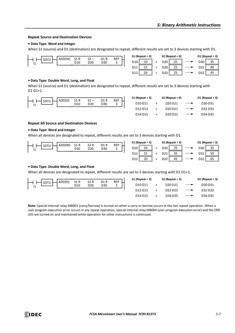
5: Binary Arithmetic Instructions
Repeat Source and Destination Devices
• Data Type: Word and Integer
When S1 (source) and D1 (destination) are designated to repeat, different results are set to 3 devices starting with D1.
• Data Type: Double Word, Long, and Float
When S1 (source) and D1 (destination) are designated to repeat, different results are set to 3 devices starting with D1∙D1+1.
Repeat All Source and Destination Devices
• Data Type: Word and Integer
When all devices are designated to repeat, different results are set to 3 devices starting with D1.
• Data Type: Double Word, Long, and Float
When all devices are designated to repeat, different results are set to 3 devices starting with D1∙D1+1.
Note: Special internal relay M8003 (carry/borrow) is turned on when a carry or borrow occurs in the last repeat operation. When a user program execution error occurs in any repeat operation, special internal relay M8004 (user program execution error) and the ERR LED are turned on and maintained while operation for other instructions is continued.
I1
REP3
S1 RD10
D1 RD30
15D11
10D10
20D12
S1 (Repeat = 3) D1 (Repeat = 3)S2 –D20
S2 (Repeat = 0)
+
+
+
40D31
35D30
45D32
25D20
25D20
25D20
SOTU ADD(W)
I1
REP3
S1 RD10
D1 RD30
D12∙D13
D10∙D11
D14∙D15
S1 (Repeat = 3) D1 (Repeat = 3)S2 –D20
S2 (Repeat = 0)
+
+
+
D32∙D33
D30∙D31
D34∙D35
D20∙D21
D20∙D21
D20∙D21
SOTU ADD(D)
I1
REP3
S1 RD10
D1 RD30
15D11
10D10
20D12
S1 (Repeat = 3) D1 (Repeat = 3)S2 RD20
S2 (Repeat = 3)
+
+
+
50D31
35D30
65D32
35D21
25D20
45D22
SOTU ADD(W)
I1
REP3
S1 RD10
D1 RD30
D12∙D13
D10∙D11
D14∙D15
S1 (Repeat = 3) D1 (Repeat = 3)S2 RD20
S2 (Repeat = 3)
+
+
+
D32∙D33
D30∙D31
D34∙D35
D22∙D23
D20∙D21
D24∙D25
SOTU ADD(D)
FC5A MicroSmart User’s Manual FC9Y‐B1273 5‐7
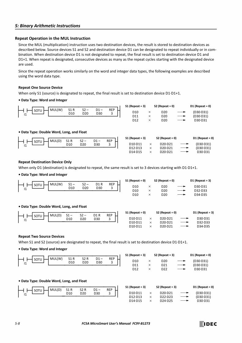
5: Binary Arithmetic Instructions
Repeat Operation in the MUL Instruction
Since the MUL (multiplication) instruction uses two destination devices, the result is stored to destination devices as described below. Source devices S1 and S2 and destination device D1 can be designated to repeat individually or in com‐bination. When destination device D1 is not designated to repeat, the final result is set to destination device D1 and D1+1. When repeat is designated, consecutive devices as many as the repeat cycles starting with the designated device are used.
Since the repeat operation works similarly on the word and integer data types, the following examples are described using the word data type.
Repeat One Source Device
When only S1 (source) is designated to repeat, the final result is set to destination device D1∙D1+1.
• Data Type: Word and Integer
• Data Type: Double Word, Long, and Float
Repeat Destination Device Only
When only D1 (destination) is designated to repeat, the same result is set to 3 devices starting with D1∙D1+1.
• Data Type: Word and Integer
• Data Type: Double Word, Long, and Float
Repeat Two Source Devices
When S1 and S2 (source) are designated to repeat, the final result is set to destination device D1∙D1+1.
• Data Type: Word and Integer
• Data Type: Double Word, Long, and Float
I1
REP3
S1 RD10
D1 –D30 D10
S1 (Repeat = 3) D1 (Repeat = 0)S2 –D20
S2 (Repeat = 0)
D20D11D12
D20D20
SOTU MUL(W)
(D30∙D31)(D30∙D31)
D30∙D31
I1
REP3
S1 RD10
D1 –D30
D12∙D13D10∙D11
D14∙D15
S1 (Repeat = 3) D1 (Repeat = 0)S2 –D20
S2 (Repeat = 0)
(D30∙D31)(D30∙D31)
D30∙D31D20∙D21D20∙D21
D20∙D21
SOTU MUL(D)
I1
REP3
S1 –D10
D1 RD30 D10
S1 (Repeat = 0) D1 (Repeat = 3)S2 –D20
S2 (Repeat = 0)
D20D10D10
D20D20
SOTU MUL(W)
D32∙D33D30∙D31
D34∙D35
I1
REP3
S1 –D10
D1 RD30
D10∙D11D10∙D11
D10∙D11
S1 (Repeat = 0) D1 (Repeat = 3)S2 –D20
S2 (Repeat = 0)
D32∙D33D30∙D31
D34∙D35D20∙D21D20∙D21
D20∙D21
SOTU MUL(D)
I1
REP3
S1 RD10
D1 –D30 D10
S1 (Repeat = 3) D1 (Repeat = 0)S2 RD20
S2 (Repeat = 3)
D20D11D12
D21D22
SOTU MUL(W)
(D30∙D31)(D30∙D31)
D30∙D31
I1
REP3
S1 RD10
D1 –D30
D12∙D13D10∙D11
D14∙D15
S1 (Repeat = 3) D1 (Repeat = 0)S2 RD20
S2 (Repeat = 3)
(D30∙D31)(D30∙D31)
D30∙D31D22∙D23D20∙D21
D24∙D25
SOTU MUL(D)
5‐8 FC5A MicroSmart User’s Manual FC9Y‐B1273
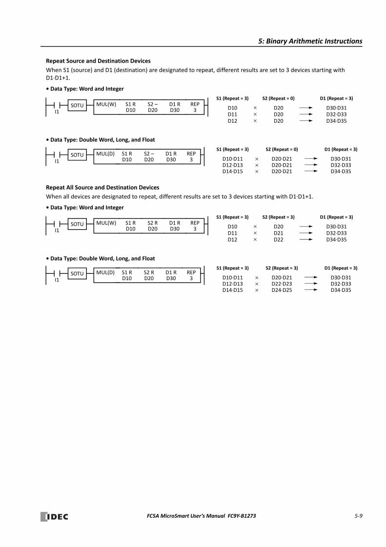
5: Binary Arithmetic Instructions
Repeat Source and Destination Devices
When S1 (source) and D1 (destination) are designated to repeat, different results are set to 3 devices starting with D1∙D1+1.
• Data Type: Word and Integer
• Data Type: Double Word, Long, and Float
Repeat All Source and Destination Devices
When all devices are designated to repeat, different results are set to 3 devices starting with D1∙D1+1.
• Data Type: Word and Integer
• Data Type: Double Word, Long, and Float
I1
REP3
S1 RD10
D1 RD30 D10
S1 (Repeat = 3) D1 (Repeat = 3)S2 –D20
S2 (Repeat = 0)
D20D11D12
D20D20
SOTU MUL(W)
D32∙D33D30∙D31
D34∙D35
I1
REP3
S1 RD10
D1 RD30
D12∙D13D10∙D11
D14∙D15
S1 (Repeat = 3) D1 (Repeat = 3)S2 –D20
S2 (Repeat = 0)
D32∙D33D30∙D31
D34∙D35D20∙D21D20∙D21
D20∙D21
SOTU MUL(D)
I1
REP3
S1 RD10
D1 RD30 D10
S1 (Repeat = 3) D1 (Repeat = 3)S2 RD20
S2 (Repeat = 3)
D20D11D12
D21D22
SOTU MUL(W)
D32∙D33D30∙D31
D34∙D35
I1
REP3
S1 RD10
D1 RD30
D12∙D13D10∙D11
D14∙D15
S1 (Repeat = 3) D1 (Repeat = 3)S2 RD20
S2 (Repeat = 3)
D32∙D33D30∙D31
D34∙D35D22∙D23D20∙D21
D24∙D25
SOTU MUL(D)
FC5A MicroSmart User’s Manual FC9Y‐B1273 5‐9
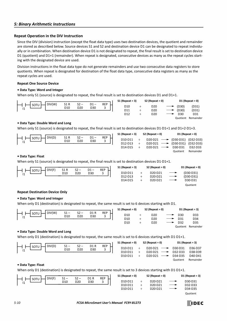
5: Binary Arithmetic Instructions
Repeat Operation in the DIV Instruction
Since the DIV (division) instruction (except the float data type) uses two destination devices, the quotient and remainder are stored as described below. Source devices S1 and S2 and destination device D1 can be designated to repeat individu‐ally or in combination. When destination device D1 is not designated to repeat, the final result is set to destination device D1 (quotient) and D1+1 (remainder). When repeat is designated, consecutive devices as many as the repeat cycles start‐ing with the designated device are used.
Division instructions in the float data type do not generate remainders and use two consecutive data registers to store quotients. When repeat is designated for destination of the float data type, consecutive data registers as many as the repeat cycles are used.
Repeat One Source Device
• Data Type: Word and Integer
When only S1 (source) is designated to repeat, the final result is set to destination devices D1 and D1+1.
• Data Type: Double Word and Long
When only S1 (source) is designated to repeat, the final result is set to destination devices D1∙D1+1 and D1+2∙D1+3.
• Data Type: Float
When only S1 (source) is designated to repeat, the final result is set to destination devices D1∙D1+1.
Repeat Destination Device Only
• Data Type: Word and Integer
When only D1 (destination) is designated to repeat, the same result is set to 6 devices starting with D1.
• Data Type: Double Word and Long
When only D1 (destination) is designated to repeat, the same result is set to 6 devices starting with D1∙D1+1.
• Data Type: Float
When only D1 (destination) is designated to repeat, the same result is set to 3 devices starting with D1∙D1+1.
I1
REP3
S1 RD10
D1 –D30 D10
S1 (Repeat = 3) D1 (Repeat = 0)S2 –D20
S2 (Repeat = 0)
÷ (D30)D20 (D31)D11D12
÷÷
D20D20
(D30)D30
(D31)D31
Quotient Remainder
SOTU DIV(W)
I1
REP3
S1 RD10
D1 –D30 D10∙D11
S1 (Repeat = 3) D1 (Repeat = 0)S2 –D20
S2 (Repeat = 0)
÷ (D30∙D31)D20∙D21 (D32∙D33)D12∙D13D14∙D15
÷÷
D20∙D21D20∙D21
(D30∙D31)D30∙D31
(D32∙D33)D32∙D33
Quotient Remainder
SOTU DIV(D)
I1
REP3
S1 RD10
D1 –D30
D12∙D13D10∙D11
D14∙D15
S1 (Repeat = 3) D1 (Repeat = 0)S2 –D20
S2 (Repeat = 0)
÷÷÷
(D30∙D31)(D30∙D31)
D30∙D31D20∙D21D20∙D21
D20∙D21
SOTU DIV(F)
Quotient
I1
REP3
S1 –D10
D1 RD30 D10
S1 (Repeat = 0) D1 (Repeat = 3)S2 –D20
S2 (Repeat = 0)
÷ D30D20 D33D10D10
÷÷
D20D20
D31D32
D34D35
Quotient Remainder
SOTU DIV(W)
I1
REP3
S1 –D10
D1 RD30 D10∙D11
S1 (Repeat = 0) D1 (Repeat = 3)S2 –D20
S2 (Repeat = 0)
÷ D30∙D31D20∙D21 D36∙D37D10∙D11D10∙D11
÷÷
D20∙D21D20∙D21
D32∙D33D34∙D35
D38∙D39D40∙D41
Quotient Remainder
SOTU DIV(D)
I1
REP3
S1 –D10
D1 RD30
D10∙D11D10∙D11
D10∙D11
S1 (Repeat = 0) D1 (Repeat = 3)S2 –D20
S2 (Repeat = 0)
÷÷÷
D32∙D33D30∙D31
D34∙D35D20∙D21D20∙D21
D20∙D21
SOTU DIV(F)
Quotient
5‐10 FC5A MicroSmart User’s Manual FC9Y‐B1273

5: Binary Arithmetic Instructions
Repeat Two Source Devices
• Data Type: Word and Integer
When S1 and S2 (source) are designated to repeat, the final result is set to destination devices D1 and D1+1.
• Data Type: Double Word and Long
When S1 and S2 (source) are designated to repeat, the final result is set to destination devices D1∙D1+1 and D1+2∙D1+3.
• Data Type: Float
When S1 and S2 (source) are designated to repeat, the final result is set to destination devices D1∙D1+1.
Repeat Source and Destination Devices
• Data Type: Word and Integer
When S1 (source) and D1 (destination) are designated to repeat, different results are set to 6 devices starting with D1.
• Data Type: Double Word and Long
When S1 (source) and D1 (destination) are designated to repeat, different results are set to 6 devices starting with D1∙D1+1.
• Data Type: Float
When S1 (source) and D1 (destination) are designated to repeat, different results are set to 3 devices starting with D1∙D1+1.
I1
REP3
S1 RD10
D1 –D30 D10
S1 (Repeat = 3) D1 (Repeat = 0)S2 RD20
S2 (Repeat = 3)
÷ (D30)D20 (D31)D11D12
÷÷
D21D22
(D30)D30
(D31)D31
Quotient Remainder
SOTU DIV(W)
I1
REP3
S1 RD10
D1 –D30 D10∙D11
S1 (Repeat = 3) D1 (Repeat = 0)S2 RD20
S2 (Repeat = 3)
÷ (D30∙D31)D20∙D21 (D32∙D33)D12∙D13D14∙D15
÷÷
D22∙D23D24∙D25
(D30∙D31)D30∙D31
(D32∙D33)D32∙D33
Quotient Remainder
SOTU DIV(D)
I1
REP3
S1 RD10
D1 –D30
D12∙D13D10∙D11
D14∙D15
S1 (Repeat = 3) D1 (Repeat = 0)S2 RD20
S2 (Repeat = 3)
÷÷÷
(D30∙D31)(D30∙D31)
D30∙D31D22∙D23D20∙D21
D24∙D25
SOTU DIV(F)
Quotient
I1
REP3
S1 RD10
D1 RD30 D10
S1 (Repeat = 3) D1 (Repeat = 3)S2 –D20
S2 (Repeat = 0)
÷ D30D20 D33D11D12
÷÷
D20D20
D31D32
D34D35
Quotient Remainder
SOTU DIV(W)
I1
REP3
S1 RD10
D1 RD30 D10∙D11
S1 (Repeat = 3) D1 (Repeat = 3)S2 –D20
S2 (Repeat = 0)
÷ D30∙D31D20∙D21 D36∙D37D12∙D13D14∙D15
÷÷
D20∙D21D20∙D21
D32∙D33D34∙D35
D38∙D39D40∙D41
Quotient Remainder
SOTU DIV(D)
I1
REP3
S1 RD10
D1 RD30
D12∙D13D10∙D11
D14∙D15
S1 (Repeat = 0) D1 (Repeat = 3)S2 –D20
S2 (Repeat = 0)
÷÷÷
D32∙D33D30∙D31
D34∙D35D20∙D21D20∙D21
D20∙D21
SOTU DIV(F)
Quotient
FC5A MicroSmart User’s Manual FC9Y‐B1273 5‐11
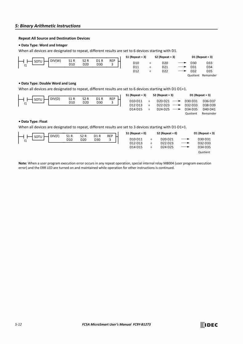
5: Binary Arithmetic Instructions
Repeat All Source and Destination Devices
• Data Type: Word and Integer
When all devices are designated to repeat, different results are set to 6 devices starting with D1.
• Data Type: Double Word and Long
When all devices are designated to repeat, different results are set to 6 devices starting with D1∙D1+1.
• Data Type: Float
When all devices are designated to repeat, different results are set to 3 devices starting with D1∙D1+1.
Note: When a user program execution error occurs in any repeat operation, special internal relay M8004 (user program execution error) and the ERR LED are turned on and maintained while operation for other instructions is continued.
I1
REP3
S1 RD10
D1 RD30 D10
S1 (Repeat = 3) D1 (Repeat = 3)S2 RD20
S2 (Repeat = 3)
÷ D30D20 D33D11D12
÷÷
D21D22
D31D32
D34D35
Quotient Remainder
SOTU DIV(W)
I1
REP3
S1 RD10
D1 RD30 D10∙D11
S1 (Repeat = 3) D1 (Repeat = 3)S2 RD20
S2 (Repeat = 3)
÷ D30∙D31D20∙D21 D36∙D37D12∙D13D14∙D15
÷÷
D22∙D23D24∙D25
D32∙D33D34∙D35
D38∙D39D40∙D41
Quotient Remainder
SOTU DIV(D)
I1
REP3
S1 RD10
D1 RD30
D12∙D13D10∙D11
D14∙D15
S1 (Repeat = 0) D1 (Repeat = 3)S2 RD20
S2 (Repeat = 0)
÷÷÷
D32∙D33D30∙D31
D34∙D35D22∙D23D20∙D21
D24∙D25
SOTU DIV(F)
Quotient
5‐12 FC5A MicroSmart User’s Manual FC9Y‐B1273
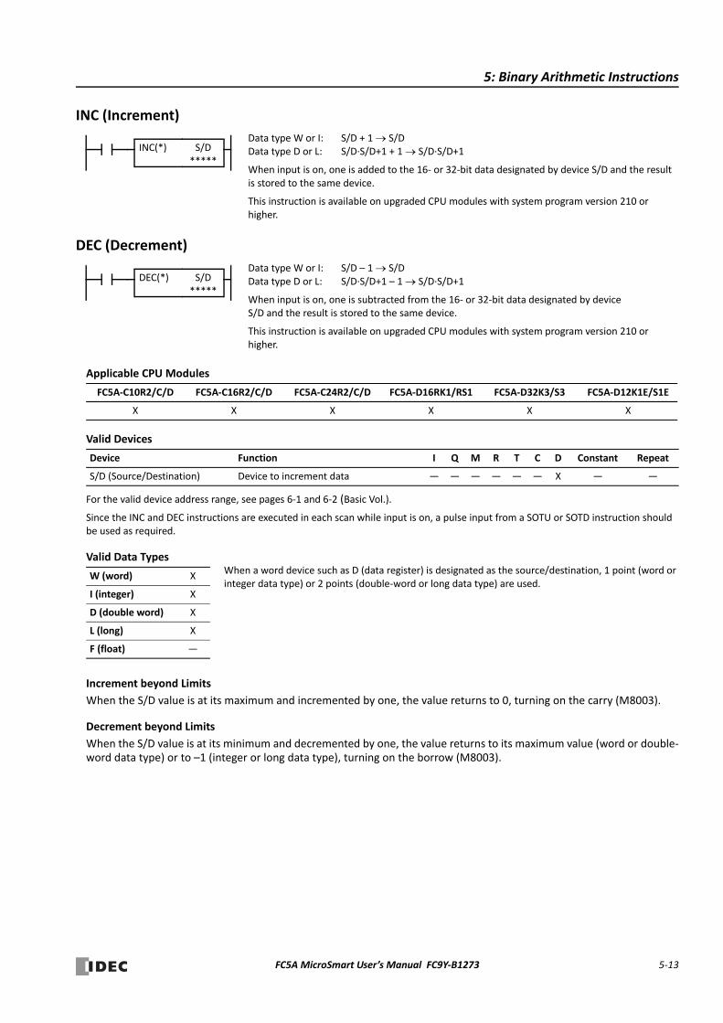
5: Binary Arithmetic Instructions
INC (Increment)
DEC (Decrement)
Applicable CPU Modules
Valid Devices
For the valid device address range, see pages 6‐1 and 6‐2 (Basic Vol.).
Since the INC and DEC instructions are executed in each scan while input is on, a pulse input from a SOTU or SOTD instruction should be used as required.
Valid Data Types
Increment beyond Limits
When the S/D value is at its maximum and incremented by one, the value returns to 0, turning on the carry (M8003).
Decrement beyond Limits
When the S/D value is at its minimum and decremented by one, the value returns to its maximum value (word or double‐word data type) or to –1 (integer or long data type), turning on the borrow (M8003).
FC5A‐C10R2/C/D FC5A‐C16R2/C/D FC5A‐C24R2/C/D FC5A‐D16RK1/RS1 FC5A‐D32K3/S3 FC5A‐D12K1E/S1E
X X X X X X
Device Function I Q M R T C D Constant Repeat
S/D (Source/Destination) Device to increment data — — — — — — X — —
W (word) X
I (integer) X
D (double word) X
L (long) X
F (float) —
Data type W or I: S/D + 1 S/DData type D or L: S/D∙S/D+1 + 1 S/D∙S/D+1
When input is on, one is added to the 16‐ or 32‐bit data designated by device S/D and the result is stored to the same device.
This instruction is available on upgraded CPU modules with system program version 210 or higher.
INC(*) S/D*****
Data type W or I: S/D – 1 S/DData type D or L: S/D∙S/D+1 – 1 S/D∙S/D+1
When input is on, one is subtracted from the 16‐ or 32‐bit data designated by device S/D and the result is stored to the same device.
This instruction is available on upgraded CPU modules with system program version 210 or higher.
DEC(*) S/D*****
When a word device such as D (data register) is designated as the source/destination, 1 point (word or integer data type) or 2 points (double‐word or long data type) are used.
FC5A MicroSmart User’s Manual FC9Y‐B1273 5‐13
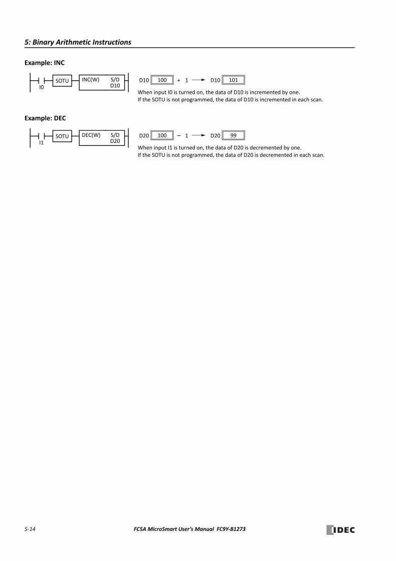
5: Binary Arithmetic Instructions
Example: INC
Example: DEC
S/DD10
When input I0 is turned on, the data of D10 is incremented by one.If the SOTU is not programmed, the data of D10 is incremented in each scan.
I0
INC(W)SOTU 100D10 + 101D101
S/DD20I1
DEC(W)SOTU
When input I1 is turned on, the data of D20 is decremented by one.If the SOTU is not programmed, the data of D20 is decremented in each scan.
100D20 – 99D201
5‐14 FC5A MicroSmart User’s Manual FC9Y‐B1273
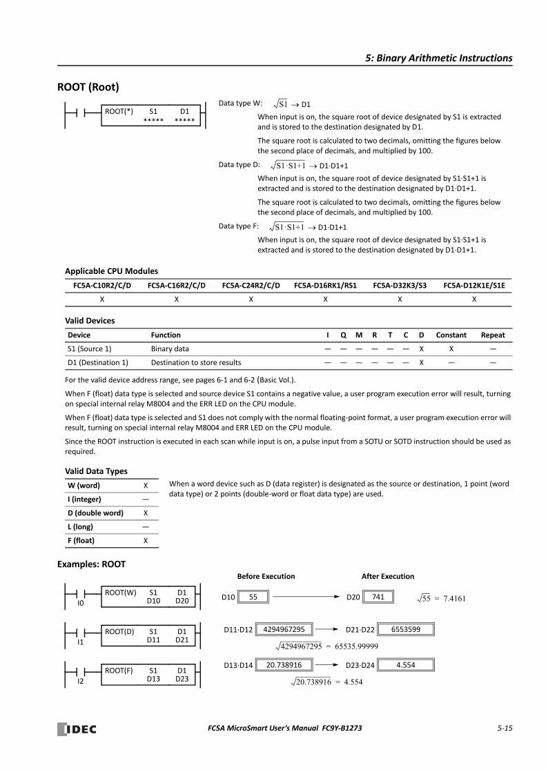
5: Binary Arithmetic Instructions
ROOT (Root)
Applicable CPU Modules
Valid Devices
For the valid device address range, see pages 6‐1 and 6‐2 (Basic Vol.).
When F (float) data type is selected and source device S1 contains a negative value, a user program execution error will result, turning on special internal relay M8004 and the ERR LED on the CPU module.
When F (float) data type is selected and S1 does not comply with the normal floating‐point format, a user program execution error will result, turning on special internal relay M8004 and ERR LED on the CPU module.
Since the ROOT instruction is executed in each scan while input is on, a pulse input from a SOTU or SOTD instruction should be used as required.
Valid Data Types
Examples: ROOT
FC5A‐C10R2/C/D FC5A‐C16R2/C/D FC5A‐C24R2/C/D FC5A‐D16RK1/RS1 FC5A‐D32K3/S3 FC5A‐D12K1E/S1E
X X X X X X
Device Function I Q M R T C D Constant Repeat
S1 (Source 1) Binary data — — — — — — X X —
D1 (Destination 1) Destination to store results — — — — — — X — —
W (word) X
I (integer) —
D (double word) X
L (long) —
F (float) X
Data type W:
When input is on, the square root of device designated by S1 is extracted and is stored to the destination designated by D1.
The square root is calculated to two decimals, omitting the figures below the second place of decimals, and multiplied by 100.
Data type D:
When input is on, the square root of device designated by S1∙S1+1 is extracted and is stored to the destination designated by D1∙D1+1.
The square root is calculated to two decimals, omitting the figures below the second place of decimals, and multiplied by 100.
Data type F:
When input is on, the square root of device designated by S1∙S1+1 is extracted and is stored to the destination designated by D1∙D1+1.
S1 D1
S1·S1+1 D1∙D1+1
S1·S1+1 D1∙D1+1
ROOT(*) S1*****
D1*****
When a word device such as D (data register) is designated as the source or destination, 1 point (word data type) or 2 points (double‐word or float data type) are used.
D1D20I0
ROOT(W) S1D10 55D10 741D20
Before Execution After Execution
D1D21I1
ROOT(D) S1D11
D1D23I2
ROOT(F) S1D13
55 7.4161=
4294967295D11∙D12 6553599D21∙D22
4294967295 65535.99999=
20.738916D13∙D14 4.554D23∙D24
20.738916 4.554=
FC5A MicroSmart User’s Manual FC9Y‐B1273 5‐15
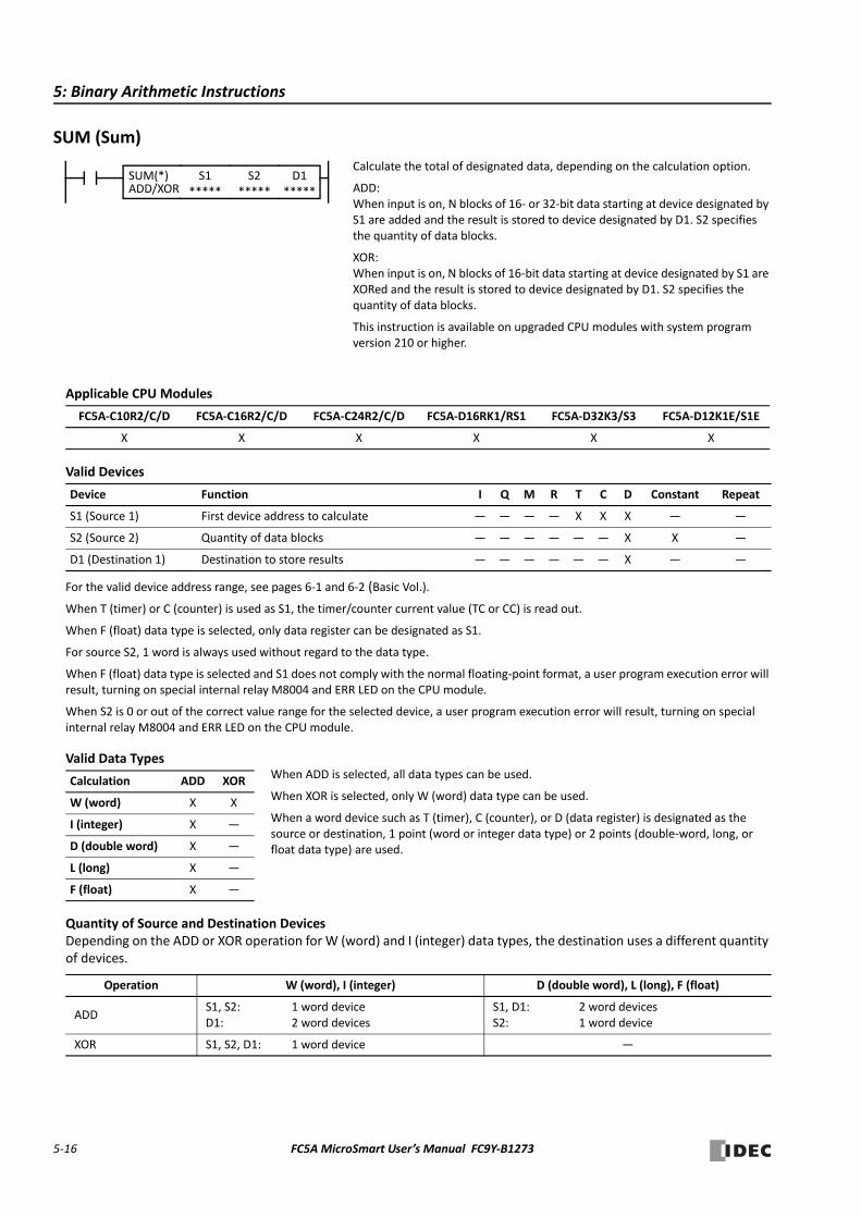
5: Binary Arithmetic Instructions
SUM (Sum)
Applicable CPU Modules
Valid Devices
For the valid device address range, see pages 6‐1 and 6‐2 (Basic Vol.).
When T (timer) or C (counter) is used as S1, the timer/counter current value (TC or CC) is read out.
When F (float) data type is selected, only data register can be designated as S1.
For source S2, 1 word is always used without regard to the data type.
When F (float) data type is selected and S1 does not comply with the normal floating‐point format, a user program execution error will result, turning on special internal relay M8004 and ERR LED on the CPU module.
When S2 is 0 or out of the correct value range for the selected device, a user program execution error will result, turning on special internal relay M8004 and ERR LED on the CPU module.
Valid Data Types
Quantity of Source and Destination DevicesDepending on the ADD or XOR operation for W (word) and I (integer) data types, the destination uses a different quantity of devices.
FC5A‐C10R2/C/D FC5A‐C16R2/C/D FC5A‐C24R2/C/D FC5A‐D16RK1/RS1 FC5A‐D32K3/S3 FC5A‐D12K1E/S1E
X X X X X X
Device Function I Q M R T C D Constant Repeat
S1 (Source 1) First device address to calculate — — — — X X X — —
S2 (Source 2) Quantity of data blocks — — — — — — X X —
D1 (Destination 1) Destination to store results — — — — — — X — —
Calculation ADD XOR
W (word) X X
I (integer) X —
D (double word) X —
L (long) X —
F (float) X —
Operation W (word), I (integer) D (double word), L (long), F (float)
ADDS1, S2: 1 word deviceD1: 2 word devices
S1, D1: 2 word devicesS2: 1 word device
XOR S1, S2, D1: 1 word device —
Calculate the total of designated data, depending on the calculation option.
ADD:When input is on, N blocks of 16‐ or 32‐bit data starting at device designated by S1 are added and the result is stored to device designated by D1. S2 specifies the quantity of data blocks.
XOR:When input is on, N blocks of 16‐bit data starting at device designated by S1 are XORed and the result is stored to device designated by D1. S2 specifies the quantity of data blocks.
This instruction is available on upgraded CPU modules with system program version 210 or higher.
D1*****
S1*****
S2*****
SUM(*)ADD/XOR
When ADD is selected, all data types can be used.
When XOR is selected, only W (word) data type can be used.
When a word device such as T (timer), C (counter), or D (data register) is designated as the source or destination, 1 point (word or integer data type) or 2 points (double‐word, long, or float data type) are used.
5‐16 FC5A MicroSmart User’s Manual FC9Y‐B1273
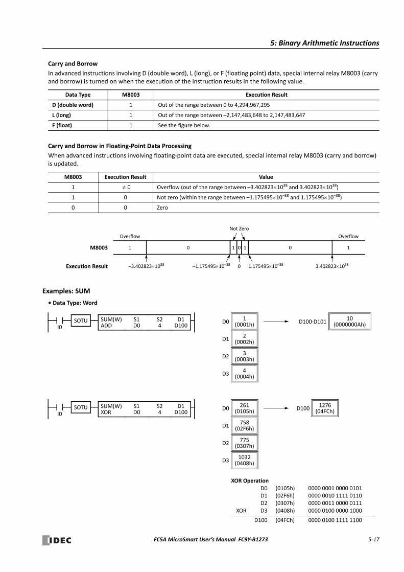
5: Binary Arithmetic Instructions
Carry and Borrow
In advanced instructions involving D (double word), L (long), or F (floating point) data, special internal relay M8003 (carry and borrow) is turned on when the execution of the instruction results in the following value.
Carry and Borrow in Floating‐Point Data Processing
When advanced instructions involving floating‐point data are executed, special internal relay M8003 (carry and borrow) is updated.
Examples: SUM
• Data Type: Word
Data Type M8003 Execution Result
D (double word) 1 Out of the range between 0 to 4,294,967,295
L (long) 1 Out of the range between –2,147,483,648 to 2,147,483,647
F (float) 1 See the figure below.
M8003 Execution Result Value
1 0 Overflow (out of the range between –3.4028231038 and 3.4028231038)
1 0 Not zero (within the range between –1.17549510–38 and 1.17549510–38)
0 0 Zero
0
–1.17549510–38
M8003 1 1
1.17549510–380–3.4028231038
0
Execution Result
1
Overflow
0 1
3.4028231038
Overflow
Not Zero
D1D100
S1D0I0
SUM(W)ADD
S24
SOTU 1D0 (0001h)
2D1 (0002h)
3D2 (0003h)
4D3 (0004h)
10(0000000Ah)D100∙D101
D1D100
S1D0I0
SUM(W)XOR
S24
SOTU 261D0 (0105h)
758D1 (02F6h)
775D2 (0307h)
1032D3 (0408h)
1276D100 (04FCh)
XOR Operation D0 (0105h) 0000 0001 0000 0101D1 (02F6h) 0000 0010 1111 0110D2 (0307h) 0000 0011 0000 0111
XOR D3 (0408h) 0000 0100 0000 1000
D100 (04FCh) 0000 0100 1111 1100
FC5A MicroSmart User’s Manual FC9Y‐B1273 5‐17

5: Binary Arithmetic Instructions
• Data Type: Integer
• Data Type: Double Word
• Data Type: Long
• Data Type: Float
D1D100
S1D0I0
SUM(I)ADD
S24
SOTU –500D0 (FE0Ch)
25D1 (0019h)
–4095D2 (F001h)
4D3 (0004h)
–4566(FFFFEE2Ah)D100∙D101
D1D100
S1D0I0
SUM(D)ADD
S24
SOTU 1000000(000F4240h)D100∙D101
100000(000186A0h)D0∙D1
200000(00030D40h)D2∙D3
300000(000493E0h)D4∙D5
400000(00061A80h)D6∙D7
D1D100
S1D0I0
SUM(L)ADD
S24
SOTU –10253086(FF638CE2h)D100∙D101
–500000(FFF85EE0h)D0∙D1
123456(0001E240h)D2∙D3
–9876543(FF694BC1h)D4∙D5
1(00000001h)D6∙D7
D1D100
S1D0I0
SUM(F)ADD
S24
SOTU D100∙D10112.345D0∙D1
D2∙D3
D4∙D5
D6∙D7
1.56
0.9876
3.5
18.3926
5‐18 FC5A MicroSmart User’s Manual FC9Y‐B1273
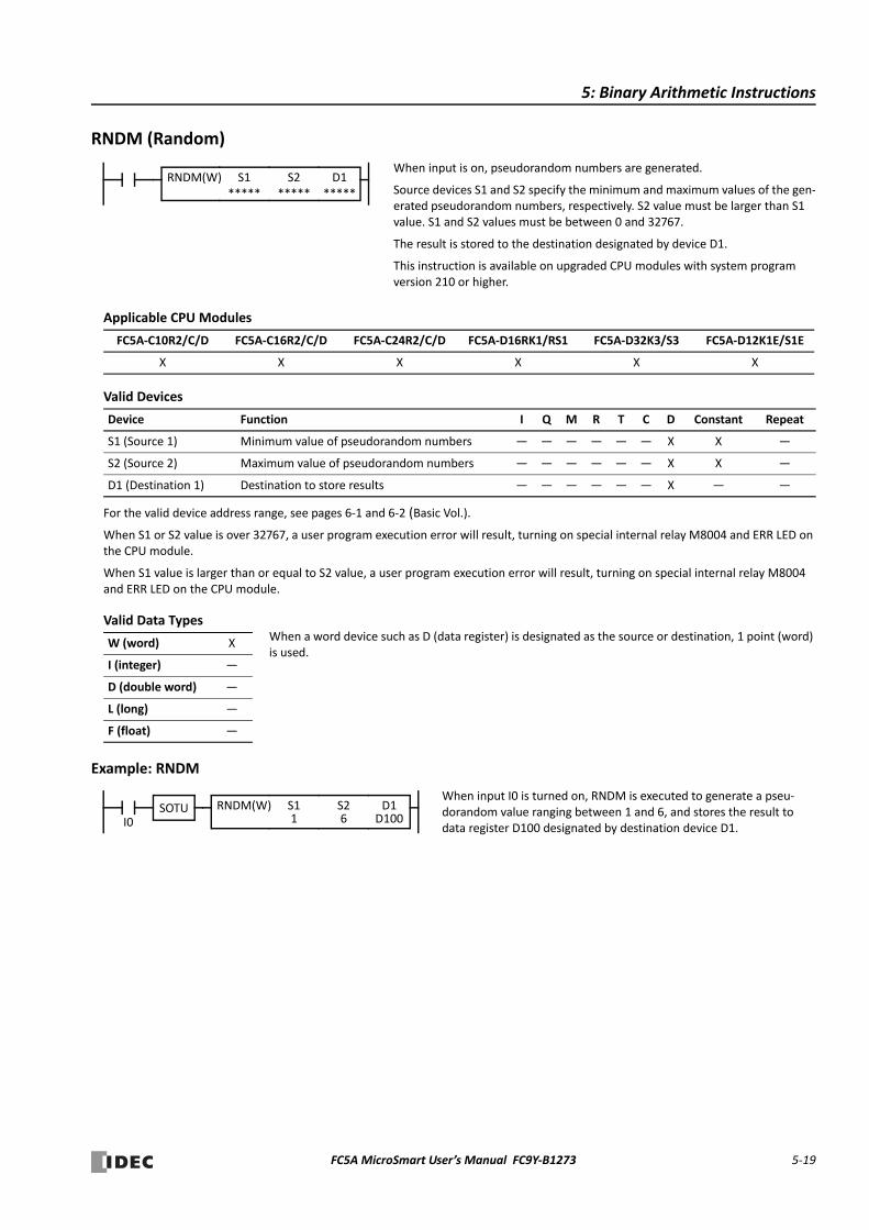
5: Binary Arithmetic Instructions
RNDM (Random)
Applicable CPU Modules
Valid Devices
For the valid device address range, see pages 6‐1 and 6‐2 (Basic Vol.).
When S1 or S2 value is over 32767, a user program execution error will result, turning on special internal relay M8004 and ERR LED on the CPU module.
When S1 value is larger than or equal to S2 value, a user program execution error will result, turning on special internal relay M8004 and ERR LED on the CPU module.
Valid Data Types
Example: RNDM
FC5A‐C10R2/C/D FC5A‐C16R2/C/D FC5A‐C24R2/C/D FC5A‐D16RK1/RS1 FC5A‐D32K3/S3 FC5A‐D12K1E/S1E
X X X X X X
Device Function I Q M R T C D Constant Repeat
S1 (Source 1) Minimum value of pseudorandom numbers — — — — — — X X —
S2 (Source 2) Maximum value of pseudorandom numbers — — — — — — X X —
D1 (Destination 1) Destination to store results — — — — — — X — —
W (word) X
I (integer) —
D (double word) —
L (long) —
F (float) —
When input is on, pseudorandom numbers are generated.
Source devices S1 and S2 specify the minimum and maximum values of the gen‐erated pseudorandom numbers, respectively. S2 value must be larger than S1 value. S1 and S2 values must be between 0 and 32767.
The result is stored to the destination designated by device D1.
This instruction is available on upgraded CPU modules with system program version 210 or higher.
D1*****
S1*****
S2*****
RNDM(W)
When a word device such as D (data register) is designated as the source or destination, 1 point (word) is used.
D1D100
S11I0
RNDM(W) S26
SOTUWhen input I0 is turned on, RNDM is executed to generate a pseu‐dorandom value ranging between 1 and 6, and stores the result to data register D100 designated by destination device D1.
FC5A MicroSmart User’s Manual FC9Y‐B1273 5‐19

5: Binary Arithmetic Instructions
5‐20 FC5A MicroSmart User’s Manual FC9Y‐B1273
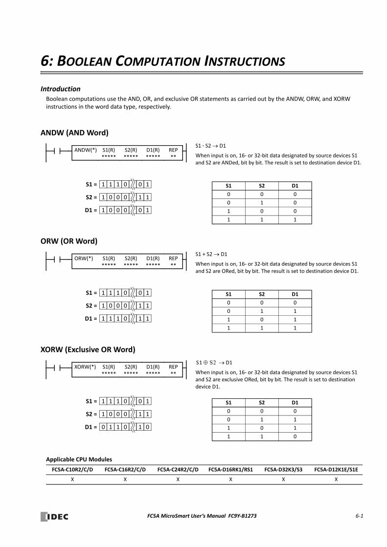
6: BOOLEAN COMPUTATION INSTRUCTIONS
IntroductionBoolean computations use the AND, OR, and exclusive OR statements as carried out by the ANDW, ORW, and XORW instructions in the word data type, respectively.
ANDW (AND Word)
ORW (OR Word)
XORW (Exclusive OR Word)
Applicable CPU Modules
FC5A‐C10R2/C/D FC5A‐C16R2/C/D FC5A‐C24R2/C/D FC5A‐D16RK1/RS1 FC5A‐D32K3/S3 FC5A‐D12K1E/S1E
X X X X X X
S1 ∙ S2 D1
When input is on, 16‐ or 32‐bit data designated by source devices S1 and S2 are ANDed, bit by bit. The result is set to destination device D1.
S1 = 1 1 1001
S2 = 1 0 1100
D1 = 1 0 1000
S1 S2 D1
0 0 0
0 1 0
1 0 0
1 1 1
REP**
S1(R)*****
D1(R)*****
ANDW(*) S2(R)*****
S1 + S2 D1
When input is on, 16‐ or 32‐bit data designated by source devices S1 and S2 are ORed, bit by bit. The result is set to destination device D1.
S1 = 1 1 1001
S2 = 1 0 1100
D1 = 1 1 1101
S1 S2 D1
0 0 0
0 1 1
1 0 1
1 1 1
REP**
S1(R)*****
D1(R)*****
ORW(*) S2(R)*****
D1
When input is on, 16‐ or 32‐bit data designated by source devices S1 and S2 are exclusive ORed, bit by bit. The result is set to destination device D1.
S1 S2
S1 = 1 1 1001
S2 = 1 0 1100
D1 = 0 1 0101
S1 S2 D1
0 0 0
0 1 1
1 0 1
1 1 0
REP**
S1(R)*****
D1(R)*****
XORW(*) S2(R)*****
FC5A MicroSmart User’s Manual FC9Y‐B1273 6‐1

6: BOOLEAN COMPUTATION INSTRUCTIONS
Valid Devices
For the valid device address range, see pages 6‐1 and 6‐2 (Basic Vol.).
Internal relays M0 through M2557 can be designated as D1. Special internal relays cannot be designated as D1.
When T (timer) or C (counter) is used as S1 or S2, the timer/counter current value (TC or CC) is read out. When T (timer) or C (counter) is used as D1, the data is written in as a preset value (TP or CP) which can be 0 through 65535.
Since the Boolean computation instructions are executed in each scan while input is on, a pulse input from a SOTU or SOTD instruction should be used as required.
Valid Data Types
Example: XORW
To convert optional output status among a series of 10 output points, use the XORW instruction in combination with 10 internal relay points.
Device Function I Q M R T C D Constant Repeat
S1 (Source 1) Data for computation X X X X X X X X 1‐99
S2 (Source 2) Data for computation X X X X X X X X 1‐99
D1 (Destination 1) Destination to store results — X X X X X — 1‐99
W (word) X
I (integer) —
D (double word) X
L (long) —
F (float) —
When a bit device such as I (input), Q (output), M (internal relay), or R (shift register) is designated as the source or destination, 16 points (word data type) or 32 points (double‐word data type) are used. When repeat is designated for a bit device, the quantity of device bits increases in 16‐ or 32‐point incre‐ments.
When a word device such as T (timer), C (counter), or D (data register) is designated as the source or destination, 1 point (word data type) or 2 points (double‐word data type) are used. When repeat is des‐ignated for a word device, the quantity of device words increases in 1‐ or 2‐point increments.
M8120
Ten outputs Q0 through Q11 are assigned to 10 internal relays M0 through M11.
Five internal relays M0, M2, M4, M6, and M10 are set by ini‐tialize pulse special internal relay M8120.
When input I1 is turned on, the XORW instruction is executed to invert the status of outputs Q0, Q2, Q4, Q6, and Q10.
0 0 00 0 0 1 10 0 1 0 1 0 1 0
Q0Q7Q10Q11
10 points
This program will invert the status of the shaded outputs at the left from on to off, and those not shaded from off to on.
REPS1 –M0
S2 –Q0
D1 –Q0
SOTUI1
M0M7M10M17
XORW(W)
M0S
M2S
M4S
M6S
M10S
6‐2 FC5A MicroSmart User’s Manual FC9Y‐B1273
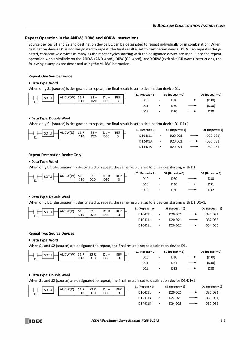
6: BOOLEAN COMPUTATION INSTRUCTIONS
Repeat Operation in the ANDW, ORW, and XORW Instructions
Source devices S1 and S2 and destination device D1 can be designated to repeat individually or in combination. When destination device D1 is not designated to repeat, the final result is set to destination device D1. When repeat is desig‐nated, consecutive devices as many as the repeat cycles starting with the designated device are used. Since the repeat operation works similarly on the ANDW (AND word), ORW (OR word), and XORW (exclusive OR word) instructions, the following examples are described using the ANDW instruction.
Repeat One Source Device
• Data Type: Word
When only S1 (source) is designated to repeat, the final result is set to destination device D1.
• Data Type: Double Word
When only S1 (source) is designated to repeat, the final result is set to destination device D1∙D1+1.
Repeat Destination Device Only
• Data Type: Word
When only D1 (destination) is designated to repeat, the same result is set to 3 devices starting with D1.
• Data Type: Double Word
When only D1 (destination) is designated to repeat, the same result is set to 3 devices starting with D1∙D1+1.
Repeat Two Source Devices
• Data Type: Word
When S1 and S2 (source) are designated to repeat, the final result is set to destination device D1.
• Data Type: Double Word
When S1 and S2 (source) are designated to repeat, the final result is set to destination device D1∙D1+1.
I1D10
S1 (Repeat = 3) D1 (Repeat = 0)S2 (Repeat = 0)
∙ (D30)D20
D11
D12
∙
∙
D20
D20
(D30)
D30
SOTU REP3
S1 RD10
D1 –D30
S2 –D20
ANDW(W)
D12∙D13
D10∙D11
D14∙D15
S1 (Repeat = 3) D1 (Repeat = 0)S2 (Repeat = 0)
∙
∙
∙
(D30∙D31)
(D30∙D31)
D30∙D31
D20∙D21
D20∙D21
D20∙D21
I1SOTU REP
3S1 RD10
D1 –D30
S2 –D20
ANDW(D)
I1
REP3
S1 –D10
D1 RD30
S2 –D20
SOTU ANDW(W)D10
S1 (Repeat = 0) D1 (Repeat = 3)S2 (Repeat = 0)
∙ D30D20
D10
D10
∙
∙
D20
D20
D31
D32
I1
REP3
S1 –D10
D1 RD30
D10∙D11
D10∙D11
D10∙D11
S1 (Repeat = 0) D1 (Repeat = 3)S2 –D20
S2 (Repeat = 0)
∙
∙
∙
D32∙D33
D30∙D31
D34∙D35
D20∙D21
D20∙D21
D20∙D21
SOTU ANDW(D)
I1
REP3
D1 –D30
S2 RD20
SOTUD10
S1 (Repeat = 3) D1 (Repeat = 0)S2 (Repeat = 3)
∙ (D30)D20
D11
D12
∙
∙
D21
D22
(D30)
D30
S1 RD10
ANDW(W)
I1
REP3
D1 –D30
D12∙D13
D10∙D11
D14∙D15
S1 (Repeat = 3) D1 (Repeat = 0)S2 RD20
S2 (Repeat = 3)
∙
∙
∙
(D30∙D31)
(D30∙D31)
D30∙D31
D22∙D23
D20∙D21
D24∙D25
SOTU S1 RD10
ANDW(D)
FC5A MicroSmart User’s Manual FC9Y‐B1273 6‐3
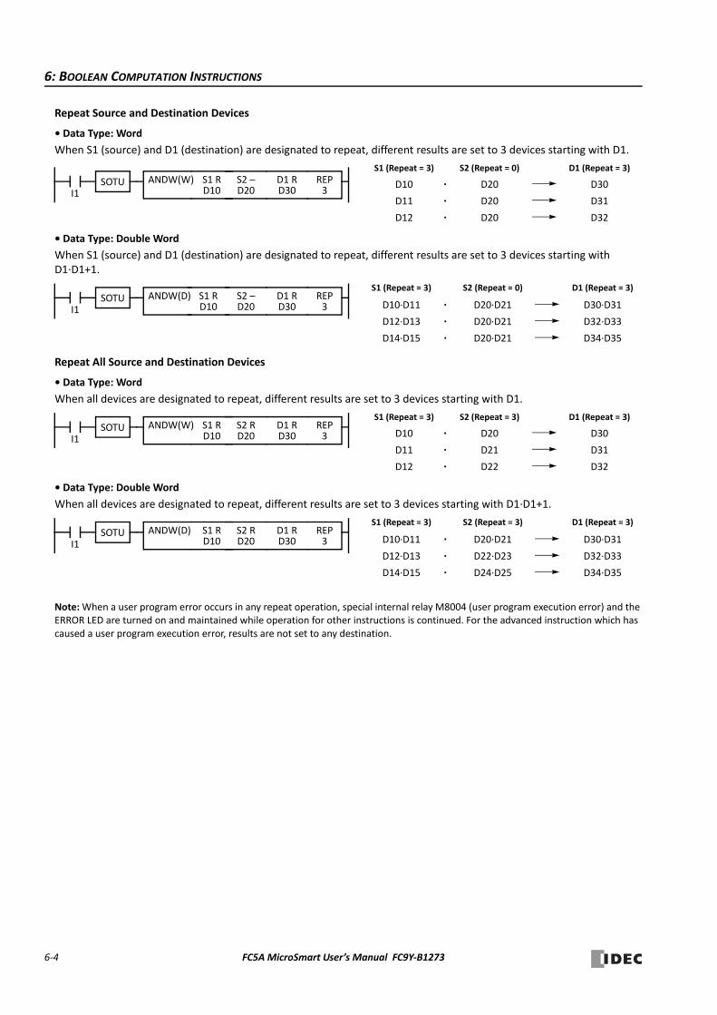
6: BOOLEAN COMPUTATION INSTRUCTIONS
Repeat Source and Destination Devices
• Data Type: Word
When S1 (source) and D1 (destination) are designated to repeat, different results are set to 3 devices starting with D1.
• Data Type: Double Word
When S1 (source) and D1 (destination) are designated to repeat, different results are set to 3 devices starting with D1∙D1+1.
Repeat All Source and Destination Devices
• Data Type: Word
When all devices are designated to repeat, different results are set to 3 devices starting with D1.
• Data Type: Double Word
When all devices are designated to repeat, different results are set to 3 devices starting with D1∙D1+1.
Note: When a user program error occurs in any repeat operation, special internal relay M8004 (user program execution error) and the ERROR LED are turned on and maintained while operation for other instructions is continued. For the advanced instruction which has caused a user program execution error, results are not set to any destination.
I1
REP3
S1 RD10
D1 RD30
S2 –D20
SOTU ANDW(W) D10
S1 (Repeat = 3) D1 (Repeat = 3)S2 (Repeat = 0)
∙ D30D20
D11
D12
∙
∙
D20
D20
D31
D32
I1
REP3
S1 RD10
D1 RD30
D12∙D13
D10∙D11
D14∙D15
S1 (Repeat = 3) D1 (Repeat = 3)S2 –D20
S2 (Repeat = 0)
∙
∙
∙
D32∙D33
D30∙D31
D34∙D35
D20∙D21
D20∙D21
D20∙D21
SOTU ANDW(D)
I1
REP3
D1 RD30
S2 RD20
SOTUD10
S1 (Repeat = 3) D1 (Repeat = 3)S2 (Repeat = 3)
∙ D30D20
D11
D12
∙
∙
D21
D22
D31
D32
S1 RD10
ANDW(W)
I1
REP3
D1 RD30
D12∙D13
D10∙D11
D14∙D15
S1 (Repeat = 3) D1 (Repeat = 3)S2 RD20
S2 (Repeat = 3)
∙
∙
∙
D32∙D33
D30∙D31
D34∙D35
D22∙D23
D20∙D21
D24∙D25
SOTU S1 RD10
ANDW(D)
6‐4 FC5A MicroSmart User’s Manual FC9Y‐B1273
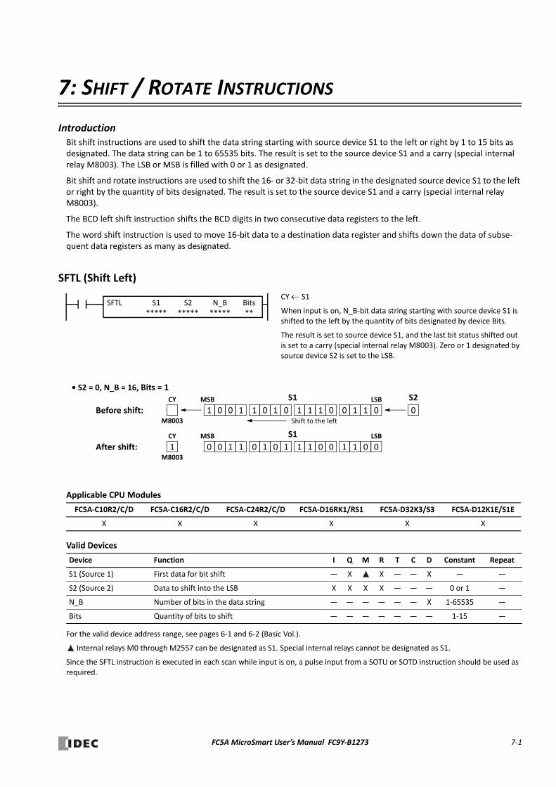
7: SHIFT / ROTATE INSTRUCTIONS
IntroductionBit shift instructions are used to shift the data string starting with source device S1 to the left or right by 1 to 15 bits as designated. The data string can be 1 to 65535 bits. The result is set to the source device S1 and a carry (special internal relay M8003). The LSB or MSB is filled with 0 or 1 as designated.
Bit shift and rotate instructions are used to shift the 16‐ or 32‐bit data string in the designated source device S1 to the left or right by the quantity of bits designated. The result is set to the source device S1 and a carry (special internal relay M8003).
The BCD left shift instruction shifts the BCD digits in two consecutive data registers to the left.
The word shift instruction is used to move 16‐bit data to a destination data register and shifts down the data of subse‐quent data registers as many as designated.
SFTL (Shift Left)
Applicable CPU Modules
Valid Devices
For the valid device address range, see pages 6‐1 and 6‐2 (Basic Vol.).
Internal relays M0 through M2557 can be designated as S1. Special internal relays cannot be designated as S1.
Since the SFTL instruction is executed in each scan while input is on, a pulse input from a SOTU or SOTD instruction should be used as required.
FC5A‐C10R2/C/D FC5A‐C16R2/C/D FC5A‐C24R2/C/D FC5A‐D16RK1/RS1 FC5A‐D32K3/S3 FC5A‐D12K1E/S1E
X X X X X X
Device Function I Q M R T C D Constant Repeat
S1 (Source 1) First data for bit shift — X X — — X — —
S2 (Source 2) Data to shift into the LSB X X X X — — — 0 or 1 —
N_B Number of bits in the data string — — — — — — X 1‐65535 —
Bits Quantity of bits to shift — — — — — — — 1‐15 —
S1*****
Bits**
CY S1
When input is on, N_B‐bit data string starting with source device S1 is shifted to the left by the quantity of bits designated by device Bits.
The result is set to source device S1, and the last bit status shifted out is set to a carry (special internal relay M8003). Zero or 1 designated by source device S2 is set to the LSB.
0Before shift: 1 0 1010 1 0 1 1 1101 0 0CY
M8003
MSB LSBS1
1After shift: 00 1010 1 0 1 1 1101 0 0CY
M8003
MSB LSBS1
Shift to the left
SFTL
• S2 = 0, N_B = 16, Bits = 1
S2*****
N_B*****
S2
FC5A MicroSmart User’s Manual FC9Y‐B1273 7‐1
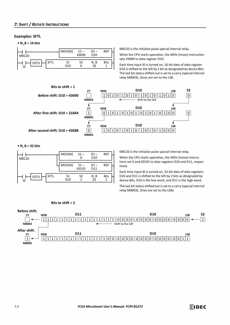
7: SHIFT / ROTATE INSTRUCTIONS
Examples: SFTL
• N_B = 16 bits
• N_B = 32 bits
M8120
REPM8120 is the initialize pulse special internal relay.
When the CPU starts operation, the MOV (move) instruction sets 43690 to data register D10.
Each time input I0 is turned on, 16‐bit data of data register D10 is shifted to the left by 1 bit as designated by device Bits. The last bit status shifted out is set to a carry (special internal relay M8003). Zeros are set to the LSB.
0Before shift: D10 = 43690 1 1 1000 1 0 1 1 1000 1 0CY
M8003
MSB LSBD10
1After first shift: D10 = 21844 01 1000 1 0 1 1 1000 1 0CY
M8003
MSB LSBD10
Bits to shift = 1
SOTUI0
S1 –43690
D1 –D10
S1D10
Bits1
0
00 0111 0 1 0 0 0111 0 00After second shift: D10 = 43688CY
M8003
MSB LSBD10
SFTL
MOV(W)
Shift to the left
S20
N_B16
S2
M8120 is the initialize pulse special internal relay.
When the CPU starts operation, the MOV (move) instruc‐tions set 0 and 65535 to data registers D10 and D11, respec‐tively.
Each time input I0 is turned on, 32‐bit data of data registers D10 and D11 is shifted to the left by 2 bits as designated by device Bits. D10 is the low word, and D11 is the high word.
The last bit status shifted out is set to a carry (special internal relay M8003). Ones are set to the LSBs.
Bits to shift = 2
1
Before shift:
0 0 0000 0 0 0 0 0000 0 0CY
M8003
MSB LSBD11
1
After shift:
10 0000 0 0 0 0 0000 0 1CY
M8003
MSB LSBD10
Shift to the left
01 1111 1 1 1 1 1111 1 0
1 1 1111 1 1 1 1 1111 1 1
M8120
REP
SOTUI0
S1 –0
D1 –D10
S1D10
Bits2
SFTL
MOV(W)
S21
N_B32
REPS1 –65535
D1 –D11
MOV(W)
D10 S2
D11
7‐2 FC5A MicroSmart User’s Manual FC9Y‐B1273
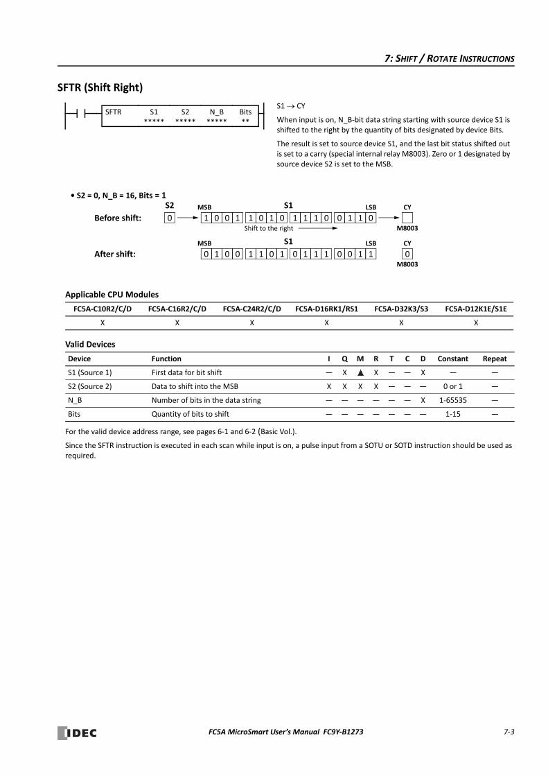
7: SHIFT / ROTATE INSTRUCTIONS
SFTR (Shift Right)
Applicable CPU Modules
Valid Devices
For the valid device address range, see pages 6‐1 and 6‐2 (Basic Vol.).
Since the SFTR instruction is executed in each scan while input is on, a pulse input from a SOTU or SOTD instruction should be used as required.
FC5A‐C10R2/C/D FC5A‐C16R2/C/D FC5A‐C24R2/C/D FC5A‐D16RK1/RS1 FC5A‐D32K3/S3 FC5A‐D12K1E/S1E
X X X X X X
Device Function I Q M R T C D Constant Repeat
S1 (Source 1) First data for bit shift — X X — — X — —
S2 (Source 2) Data to shift into the MSB X X X X — — — 0 or 1 —
N_B Number of bits in the data string — — — — — — X 1‐65535 —
Bits Quantity of bits to shift — — — — — — — 1‐15 —
S1 CY
When input is on, N_B‐bit data string starting with source device S1 is shifted to the right by the quantity of bits designated by device Bits.
The result is set to source device S1, and the last bit status shifted out is set to a carry (special internal relay M8003). Zero or 1 designated by source device S2 is set to the MSB.
0Before shift: 1 0 1010 1 0 1 1 1101 0 0CY
M8003
MSB LSBS1
0After shift: 11 1100 0 0 1 1 0010 1 1CY
M8003
MSB LSBS1
Shift to the right
• S2 = 0, N_B = 16, Bits = 1S2
S1*****
Bits**
SFTR S2*****
N_B*****
FC5A MicroSmart User’s Manual FC9Y‐B1273 7‐3
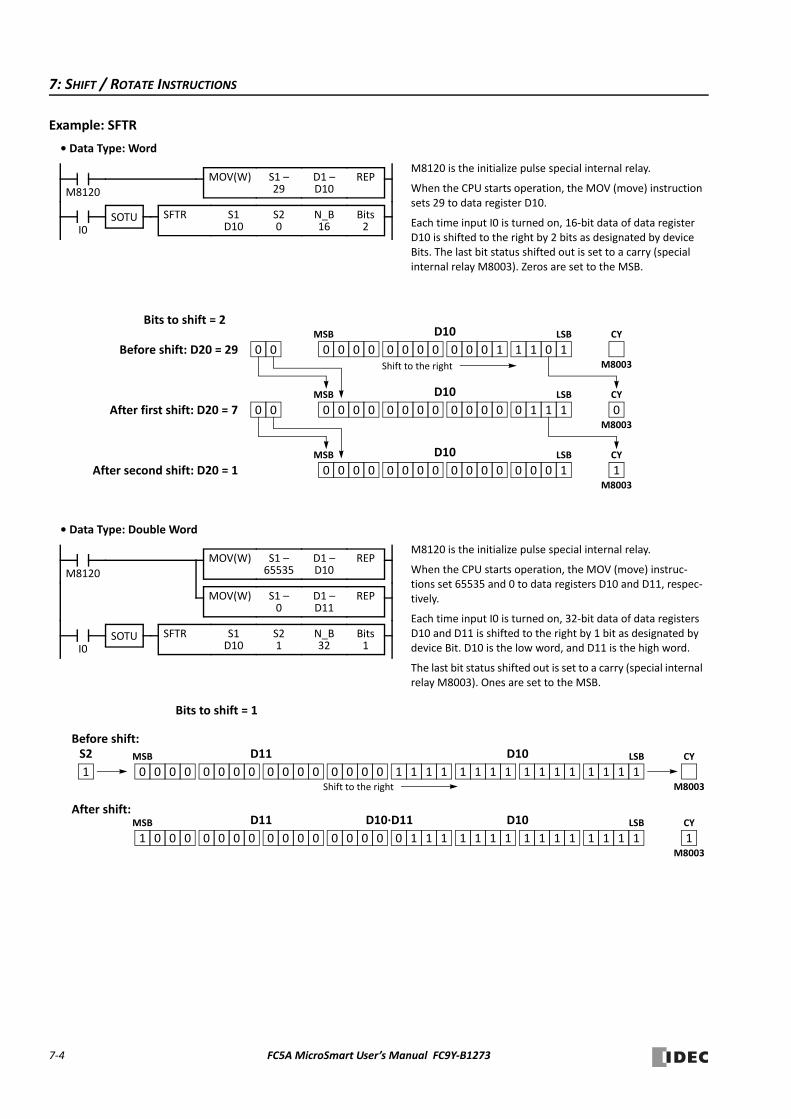
7: SHIFT / ROTATE INSTRUCTIONS
Example: SFTR
• Data Type: Word
• Data Type: Double Word
M8120
REPM8120 is the initialize pulse special internal relay.
When the CPU starts operation, the MOV (move) instruction sets 29 to data register D10.
Each time input I0 is turned on, 16‐bit data of data register D10 is shifted to the right by 2 bits as designated by device Bits. The last bit status shifted out is set to a carry (special internal relay M8003). Zeros are set to the MSB.
SOTUI0
S1 –29
D1 –D10
S1D10
Bits2
SFTR
MOV(W)
0Before shift: D20 = 29 0 0 0000 0 0 0 0 0110 1 1CY
M8003
MSB LSBD10
0After first shift: D20 = 7 10 0000 0 0 0 0 1000 0 1CY
M8003
MSB LSBD10
Bits to shift = 2
0
10 0000 0 0 0 0 0000 0 0After second shift: D20 = 1CY
M8003
MSB LSBD10
1
0
0
Shift to the right
S20
N_B16
M8120 is the initialize pulse special internal relay.
When the CPU starts operation, the MOV (move) instruc‐tions set 65535 and 0 to data registers D10 and D11, respec‐tively.
Each time input I0 is turned on, 32‐bit data of data registers D10 and D11 is shifted to the right by 1 bit as designated by device Bit. D10 is the low word, and D11 is the high word.
The last bit status shifted out is set to a carry (special internal relay M8003). Ones are set to the MSB.
Bits to shift = 1
1
Before shift:
1 1 1111 1 1 1 1 1111 1 1CY
M8003
MSB LSBD10
1
After shift:
11 1110 1 1 1 1 1111 1 1CY
M8003
MSB LSBD10∙D11
Shift to the right
00 0001 0 0 0 0 0000 0 0
0 0 0000 0 0 0 0 0000 0 0
M8120
REP
SOTUI0
S1 –65535
D1 –D10
S1D10
Bits1
SFTR
MOV(W)
S21
N_B32
REPS1 –0
D1 –D11
MOV(W)
D11
D11 D10
S2
7‐4 FC5A MicroSmart User’s Manual FC9Y‐B1273
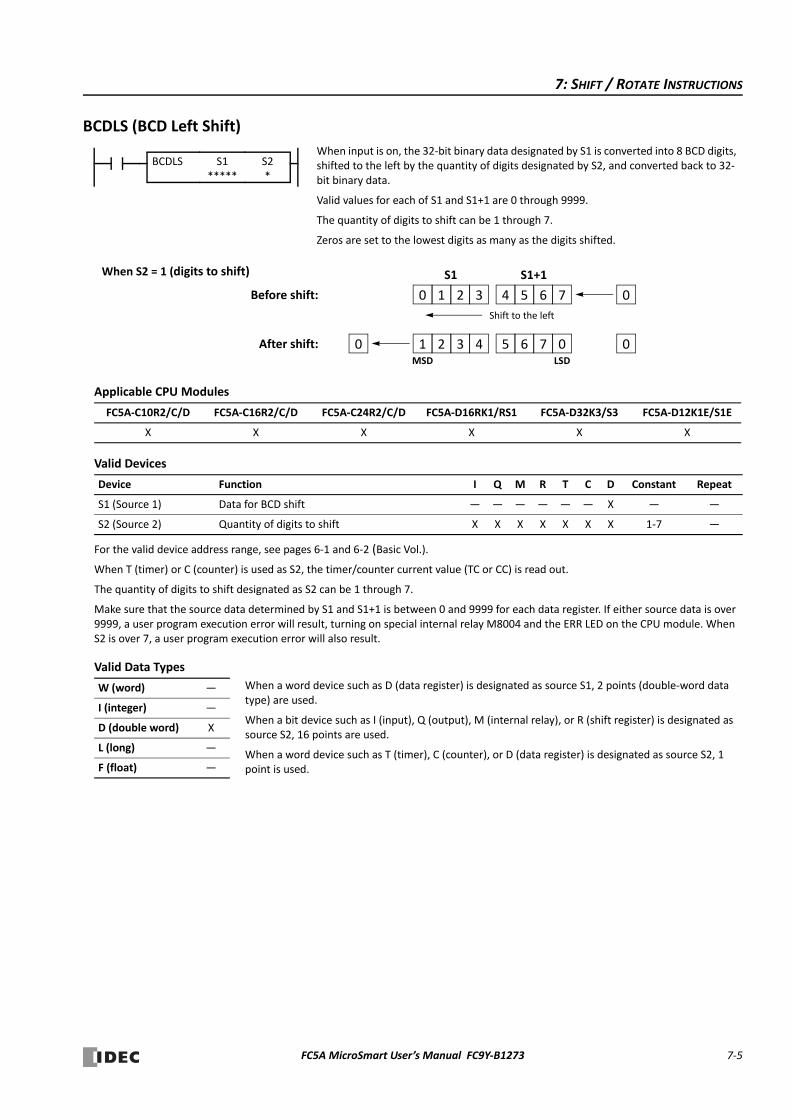
7: SHIFT / ROTATE INSTRUCTIONS
BCDLS (BCD Left Shift)
Applicable CPU Modules
Valid Devices
For the valid device address range, see pages 6‐1 and 6‐2 (Basic Vol.).
When T (timer) or C (counter) is used as S2, the timer/counter current value (TC or CC) is read out.
The quantity of digits to shift designated as S2 can be 1 through 7.
Make sure that the source data determined by S1 and S1+1 is between 0 and 9999 for each data register. If either source data is over 9999, a user program execution error will result, turning on special internal relay M8004 and the ERR LED on the CPU module. When S2 is over 7, a user program execution error will also result.
Valid Data Types
FC5A‐C10R2/C/D FC5A‐C16R2/C/D FC5A‐C24R2/C/D FC5A‐D16RK1/RS1 FC5A‐D32K3/S3 FC5A‐D12K1E/S1E
X X X X X X
Device Function I Q M R T C D Constant Repeat
S1 (Source 1) Data for BCD shift — — — — — — X — —
S2 (Source 2) Quantity of digits to shift X X X X X X X 1‐7 —
W (word) —
I (integer) —
D (double word) X
L (long) —
F (float) —
When input is on, the 32‐bit binary data designated by S1 is converted into 8 BCD digits, shifted to the left by the quantity of digits designated by S2, and converted back to 32‐bit binary data.
Valid values for each of S1 and S1+1 are 0 through 9999.
The quantity of digits to shift can be 1 through 7.
Zeros are set to the lowest digits as many as the digits shifted.
BCDLS S1*****
Before shift:
After shift:
0 2 31
MSD
S1 S1+1
Shift to the left
LSD
S2*
4 6 75 0
1 3 42 5 7 060
When S2 = 1 (digits to shift)
0
When a word device such as D (data register) is designated as source S1, 2 points (double‐word data type) are used.
When a bit device such as I (input), Q (output), M (internal relay), or R (shift register) is designated as source S2, 16 points are used.
When a word device such as T (timer), C (counter), or D (data register) is designated as source S2, 1 point is used.
FC5A MicroSmart User’s Manual FC9Y‐B1273 7‐5
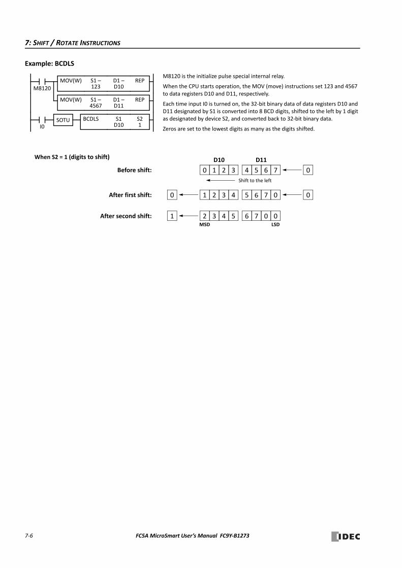
7: SHIFT / ROTATE INSTRUCTIONS
Example: BCDLS
M8120 is the initialize pulse special internal relay.
When the CPU starts operation, the MOV (move) instructions set 123 and 4567 to data registers D10 and D11, respectively.
Each time input I0 is turned on, the 32‐bit binary data of data registers D10 and D11 designated by S1 is converted into 8 BCD digits, shifted to the left by 1 digit as designated by device S2, and converted back to 32‐bit binary data.
Zeros are set to the lowest digits as many as the digits shifted.
Before shift:
After first shift:
0 2 31
D10 D11
Shift to the left
4 6 75 0
1 3 42 5 7 060
REP
SOTUI0
S1 –4567
D1 –D11
S1D10
S21
BCDLS
MOV(W)
M8120
REPS1 –123
D1 –D10
MOV(W)
After second shift:MSD LSD
2 4 53 6 0 071
0
When S2 = 1 (digits to shift)
7‐6 FC5A MicroSmart User’s Manual FC9Y‐B1273
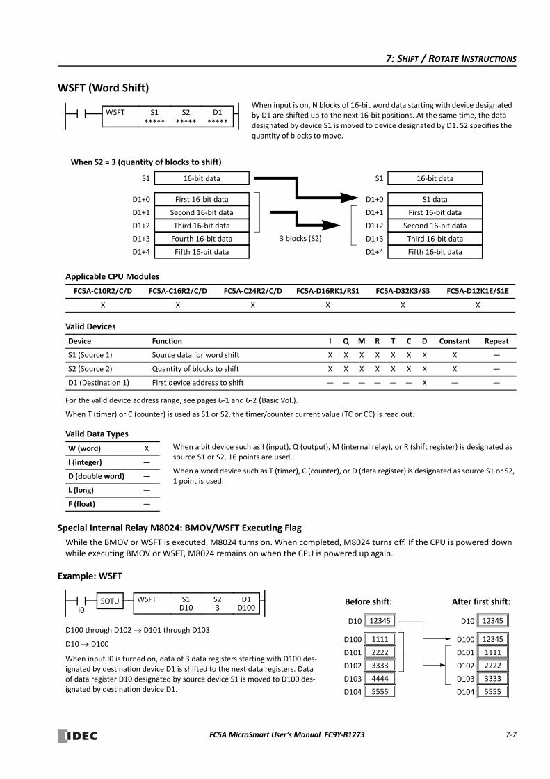
7: SHIFT / ROTATE INSTRUCTIONS
WSFT (Word Shift)
Applicable CPU Modules
Valid Devices
For the valid device address range, see pages 6‐1 and 6‐2 (Basic Vol.).
When T (timer) or C (counter) is used as S1 or S2, the timer/counter current value (TC or CC) is read out.
Valid Data Types
Special Internal Relay M8024: BMOV/WSFT Executing Flag
While the BMOV or WSFT is executed, M8024 turns on. When completed, M8024 turns off. If the CPU is powered down while executing BMOV or WSFT, M8024 remains on when the CPU is powered up again.
Example: WSFT
FC5A‐C10R2/C/D FC5A‐C16R2/C/D FC5A‐C24R2/C/D FC5A‐D16RK1/RS1 FC5A‐D32K3/S3 FC5A‐D12K1E/S1E
X X X X X X
Device Function I Q M R T C D Constant Repeat
S1 (Source 1) Source data for word shift X X X X X X X X —
S2 (Source 2) Quantity of blocks to shift X X X X X X X X —
D1 (Destination 1) First device address to shift — — — — — — X — —
W (word) X
I (integer) —
D (double word) —
L (long) —
F (float) —
When input is on, N blocks of 16‐bit word data starting with device designated by D1 are shifted up to the next 16‐bit positions. At the same time, the data designated by device S1 is moved to device designated by D1. S2 specifies the quantity of blocks to move.
WSFT S1*****
D1*****
S2*****
When S2 = 3 (quantity of blocks to shift)
First 16‐bit dataD1+0
Second 16‐bit dataD1+1
Third 16‐bit dataD1+2
Fifth 16‐bit dataD1+4
Fourth 16‐bit dataD1+3
S1 dataD1+0
First 16‐bit dataD1+1
Second 16‐bit dataD1+2
Fifth 16‐bit dataD1+4
Third 16‐bit dataD1+33 blocks (S2)
16‐bit dataS1 16‐bit dataS1
When a bit device such as I (input), Q (output), M (internal relay), or R (shift register) is designated as source S1 or S2, 16 points are used.
When a word device such as T (timer), C (counter), or D (data register) is designated as source S1 or S2, 1 point is used.
D100 through D102 D101 through D103
D10 D100
When input I0 is turned on, data of 3 data registers starting with D100 des‐ignated by destination device D1 is shifted to the next data registers. Data of data register D10 designated by source device S1 is moved to D100 des‐ignated by destination device D1.
SOTUI0
S1D10
D1D100
WSFT S23
2222D101
1111D100
3333D102
4444D103
5555D104
1111D101
12345D100
2222D102
3333D103
5555D104
12345D10 12345D10
Before shift: After first shift:
FC5A MicroSmart User’s Manual FC9Y‐B1273 7‐7
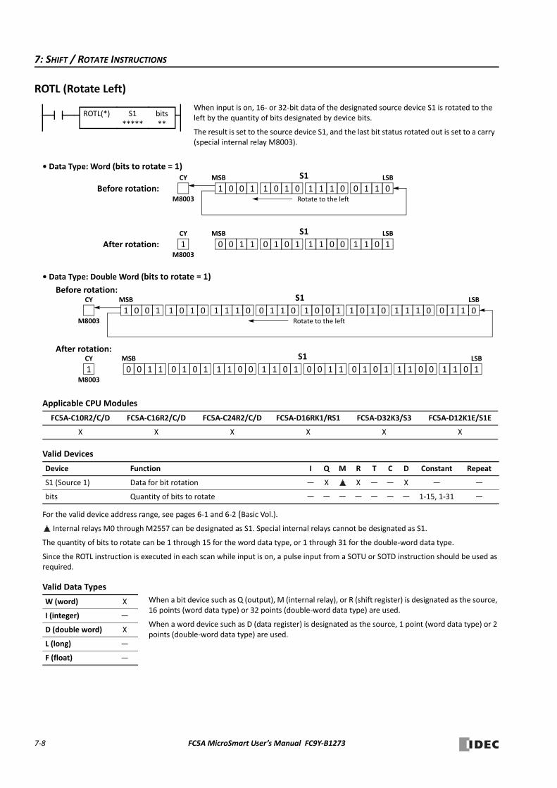
7: SHIFT / ROTATE INSTRUCTIONS
ROTL (Rotate Left)
Applicable CPU Modules
Valid Devices
For the valid device address range, see pages 6‐1 and 6‐2 (Basic Vol.).
Internal relays M0 through M2557 can be designated as S1. Special internal relays cannot be designated as S1.
The quantity of bits to rotate can be 1 through 15 for the word data type, or 1 through 31 for the double‐word data type.
Since the ROTL instruction is executed in each scan while input is on, a pulse input from a SOTU or SOTD instruction should be used as required.
Valid Data Types
FC5A‐C10R2/C/D FC5A‐C16R2/C/D FC5A‐C24R2/C/D FC5A‐D16RK1/RS1 FC5A‐D32K3/S3 FC5A‐D12K1E/S1E
X X X X X X
Device Function I Q M R T C D Constant Repeat
S1 (Source 1) Data for bit rotation — X X — — X — —
bits Quantity of bits to rotate — — — — — — — 1‐15, 1‐31 —
W (word) X
I (integer) —
D (double word) X
L (long) —
F (float) —
Before rotation: 1 0 1010 1 0 1 1 1101 0 0CY
M8003
MSB LSBS1
1After rotation: 0 1010 1 0 1 1 1101 0 0CY
M8003
MSB LSBS1
1
Rotate to the left
S1*****
bits**
When input is on, 16‐ or 32‐bit data of the designated source device S1 is rotated to the left by the quantity of bits designated by device bits.
The result is set to the source device S1, and the last bit status rotated out is set to a carry (special internal relay M8003).
ROTL(*)
• Data Type: Word (bits to rotate = 1)
Before rotation:
1 0 1010 1 0 1 1 1101 0 0CY
M8003
MSB LSBS1
1
After rotation:
10 1010 1 0 1 1 1101 0 0CY
M8003
MSB LSBS1
Rotate to the left
10 1010 1 0 1 1 1101 0 0
1 0 1010 1 0 1 1 1101 0 0
• Data Type: Double Word (bits to rotate = 1)
When a bit device such as Q (output), M (internal relay), or R (shift register) is designated as the source, 16 points (word data type) or 32 points (double‐word data type) are used.
When a word device such as D (data register) is designated as the source, 1 point (word data type) or 2 points (double‐word data type) are used.
7‐8 FC5A MicroSmart User’s Manual FC9Y‐B1273
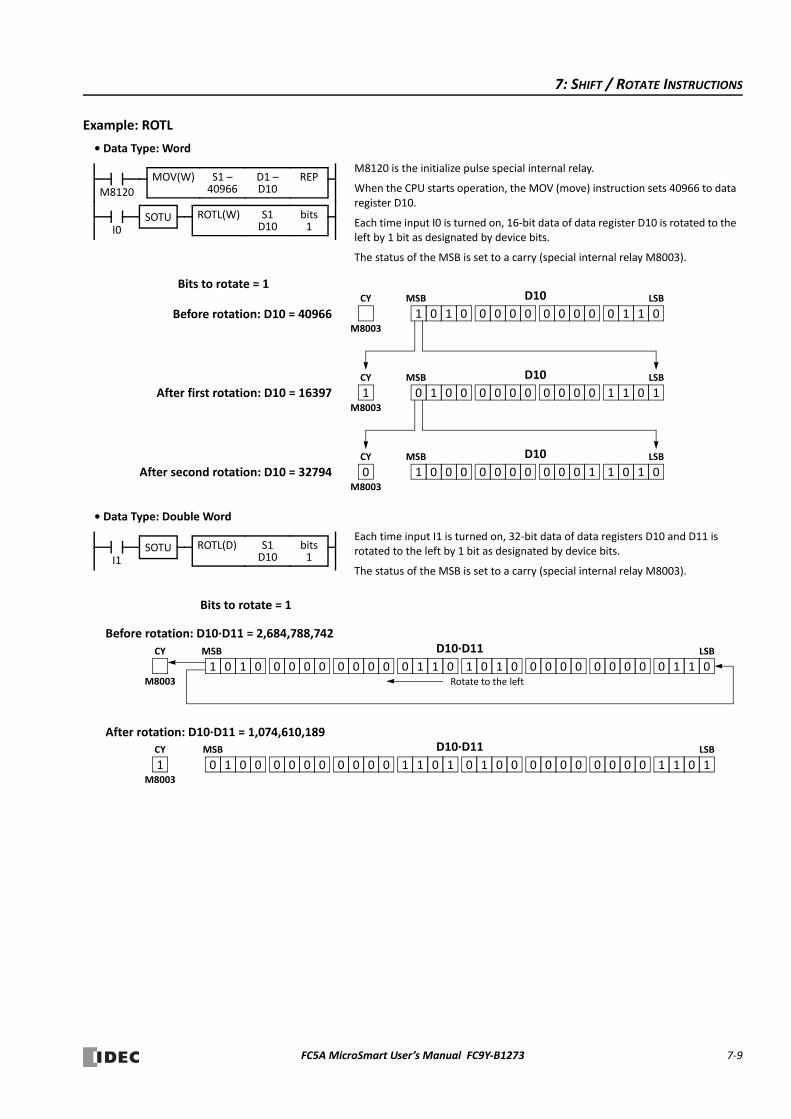
7: SHIFT / ROTATE INSTRUCTIONS
Example: ROTL
• Data Type: Word
• Data Type: Double Word
Before rotation: D10 = 40966 1 1 0000 0 0 0 0 1100 0 0CY
M8003
MSB LSBD10
After first rotation: D10 = 16397
Bits to rotate = 1
After second rotation: D10 = 32794
1 0 0 0001 0 0 0 0 0100 1 1CY
M8003
MSB LSBD10
0 1 0 0000 0 0 0 0 1010 1 0CY
M8003
MSB LSBD10
M8120
REPM8120 is the initialize pulse special internal relay.
When the CPU starts operation, the MOV (move) instruction sets 40966 to data register D10.
Each time input I0 is turned on, 16‐bit data of data register D10 is rotated to the left by 1 bit as designated by device bits.
The status of the MSB is set to a carry (special internal relay M8003).
SOTUI0
S1 –40966
D1 –D10
S1D10
bits1
ROTL(W)
MOV(W)
Each time input I1 is turned on, 32‐bit data of data registers D10 and D11 is rotated to the left by 1 bit as designated by device bits.
The status of the MSB is set to a carry (special internal relay M8003).
Bits to rotate = 1
SOTUI1
S1D10
bits1
ROTL(D)
Before rotation: D10∙D11 = 2,684,788,742
After rotation: D10∙D11 = 1,074,610,189
1 1 0000 0 0 0 0 1100 0 0CY
M8003
MSB LSBD10∙D11
1 11 0000 0 0 0 0 1100 0 0CY
M8003
MSB LSBD10∙D11
Rotate to the left
11 0000 0 0 0 0 1100 0 0
1 1 0000 0 0 0 0 1100 0 0
FC5A MicroSmart User’s Manual FC9Y‐B1273 7‐9
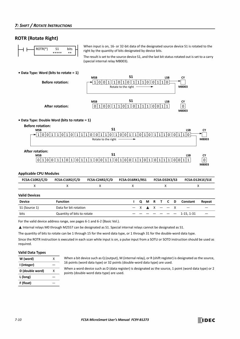
7: SHIFT / ROTATE INSTRUCTIONS
ROTR (Rotate Right)
Applicable CPU Modules
Valid Devices
For the valid device address range, see pages 6‐1 and 6‐2 (Basic Vol.).
Internal relays M0 through M2557 can be designated as S1. Special internal relays cannot be designated as S1.
The quantity of bits to rotate can be 1 through 15 for the word data type, or 1 through 31 for the double‐word data type.
Since the ROTR instruction is executed in each scan while input is on, a pulse input from a SOTU or SOTD instruction should be used as required.
Valid Data Types
FC5A‐C10R2/C/D FC5A‐C16R2/C/D FC5A‐C24R2/C/D FC5A‐D16RK1/RS1 FC5A‐D32K3/S3 FC5A‐D12K1E/S1E
X X X X X X
Device Function I Q M R T C D Constant Repeat
S1 (Source 1) Data for bit rotation — X X — — X — —
bits Quantity of bits to rotate — — — — — — — 1‐15, 1‐31 —
W (word) X
I (integer) —
D (double word) X
L (long) —
F (float) —
Before rotation: 1 0 1010 1 0 1 1 1101 0 0CY
M8003
MSB LSBS1
0After rotation: 1 1100 0 0 1 1 0010 1 1CY
M8003
MSB LSBS1
1
Rotate to the right
S1*****
bits**
When input is on, 16‐ or 32‐bit data of the designated source device S1 is rotated to the right by the quantity of bits designated by device bits.
The result is set to the source device S1, and the last bit status rotated out is set to a carry (special internal relay M8003).
ROTR(*)
• Data Type: Word (bits to rotate = 1)
Before rotation:
1 0 1010 1 0 1 1 1101 0 0CY
M8003
MSB LSBS1
0
After rotation:CY
M8003
MSB LSBS1
Rotate to the right
1 0 1010 1 0 1 1 1101 0 0
• Data Type: Double Word (bits to rotate = 1)
1 1100 0 0 1 1 0010 1 1 1 1 1100 0 0 1 1 0010 1 1 1
When a bit device such as Q (output), M (internal relay), or R (shift register) is designated as the source, 16 points (word data type) or 32 points (double‐word data type) are used.
When a word device such as D (data register) is designated as the source, 1 point (word data type) or 2 points (double‐word data type) are used.
7‐10 FC5A MicroSmart User’s Manual FC9Y‐B1273

7: SHIFT / ROTATE INSTRUCTIONS
Example: ROTR
• Data Type: Word
• Data Type: Double Word
Before rotation: D20 = 13 0 0 0000 0 0 0 0 0100 1 1CY
M8003
MSB LSBD20
After first rotation: D20 = 16387
Bits to rotate = 2
After second rotation: D20 = 53248
00 0 0001 0 0 0 0 1000 0 1CY
M8003
MSB LSBD20
11 0 0011 0 0 0 0 0000 0 0CY
M8003
MSB LSBD20
M8120
REPM8120 is the initialize pulse special internal relay.
When the CPU starts operation, the MOV (move) instruction sets 13 to data reg‐ister D20.
Each time input I1 is turned on, 16‐bit data of data register D20 is rotated to the right by 2 bits as designated by device bits.
The last bit status rotated out is set to a carry (special internal relay M8003).
SOTUI1
S1 –13
D1 –D20
S1D20
bits2
ROTR(W)
MOV(W)
Each time input I1 is turned on, 32‐bit data of data registers D20 and D21 is rotated to the right by 1 bit as designated by device bits.
The last bit status rotated out is set to a carry (special internal relay M8003).
Bits to rotate = 1
SOTUI1
S1D20
bits1
ROTR(D)
Before rotation: D20∙D21 = 851,981
After rotation: D20∙D21 = 2,147,909,638
0 0 0000 0 0 0 0 0100 1 1CY
M8003
MSB LSBD20∙D21
1CY
M8003
MSB LSBD20∙D21
Rotate to the right
0 0 0000 0 0 0 0 0100 1 1
0 0001 0 0 0 0 1000 0 1 0 0 0001 0 0 0 0 1000 0 1 0
FC5A MicroSmart User’s Manual FC9Y‐B1273 7‐11

7: SHIFT / ROTATE INSTRUCTIONS
7‐12 FC5A MicroSmart User’s Manual FC9Y‐B1273
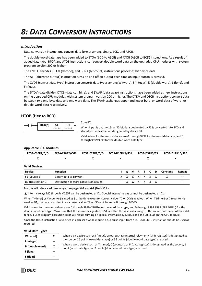
8: DATA CONVERSION INSTRUCTIONS
IntroductionData conversion instructions convert data format among binary, BCD, and ASCII.
The double‐word data type has been added to BTOA (BCD to ASCII) and ATOB (ASCII to BCD) instructions. As a result of added data type, BTOA and ATOB instructions can convert double‐word data on the upgraded CPU modules with system program version 200 or higher.
The ENCO (encode), DECO (decode), and BCNT (bit count) instructions processes bit device data.
The ALT (alternate output) instruction turns on and off an output each time an input button is pressed.
The CVDT (convert data type) instruction converts data types among W (word), I (integer), D (double word), L (long), and F (float).
The DTDV (data divide), DTCB (data combine), and SWAP (data swap) instructions have been added as new instructions on the upgraded CPU modules with system program version 200 or higher. The DTDV and DTCB instructions convert data between two one‐byte data and one word data. The SWAP exchanges upper and lower byte‐ or word‐data of word‐ or double‐word‐data respectively.
HTOB (Hex to BCD)
Applicable CPU Modules
Valid Devices
For the valid device address range, see pages 6‐1 and 6‐2 (Basic Vol.).
Internal relays M0 through M2557 can be designated as D1. Special internal relays cannot be designated as D1.
When T (timer) or C (counter) is used as S1, the timer/counter current value (TC or CC) is read out. When T (timer) or C (counter) is used as D1, the data is written in as a preset value (TP or CP) which can be 0 through 65535.
Valid values for the source device are 0 through 9999 (270Fh) for the word data type, and 0 through 9999 9999 (5F5 E0FFh) for the double‐word data type. Make sure that the source designated by S1 is within the valid value range. If the source data is out of the valid range, a user program execution error will result, turning on special internal relay M8004 and the ERR LED on the CPU module.
Since the HTOB instruction is executed in each scan while input is on, a pulse input from a SOTU or SOTD instruction should be used as required.
Valid Data Types
FC5A‐C10R2/C/D FC5A‐C16R2/C/D FC5A‐C24R2/C/D FC5A‐D16RK1/RS1 FC5A‐D32K3/S3 FC5A‐D12K1E/S1E
X X X X X X
Device Function I Q M R T C D Constant Repeat
S1 (Source 1) Binary data to convert X X X X X X X X —
D1 (Destination 1) Destination to store conversion results — X X X X X — —
W (word) X
I (integer) —
D (double word) X
L (long) —
F (float) —
S1 D1
When input is on, the 16‐ or 32‐bit data designated by S1 is converted into BCD and stored to the destination designated by device D1.
Valid values for the source device are 0 through 9999 for the word data type, and 0 through 9999 9999 for the double‐word data type.
HTOB(*) S1*****
D1*****
When a bit device such as I (input), Q (output), M (internal relay), or R (shift register) is designated as the source, 16 points (word data type) or 32 points (double‐word data type) are used.
When a word device such as T (timer), C (counter), or D (data register) is designated as the source, 1 point (word data type) or 2 points (double‐word data type) are used.
FC5A MicroSmart User’s Manual FC9Y‐B1273 8‐1

8: DATA CONVERSION INSTRUCTIONS
Examples: HTOB
• Data Type: Word
• Data Type: Double Word
D1D20
S1D10I1
HTOB(W)Binary
SOTU 0D10 (0000h)
BCD
0D20 (0000h)
1234D10 (04D2h)
4660D20 (1234h)
9999D10 (270Fh)
39321D20 (9999h)
D1D20
S1D10I2
HTOB(D)SOTU 0D10 (0000h)
0D11 (0000h)
0D20 (0000h)
0D21 (0000h)
Binary BCD
188D10 (00BCh)
24910D11 (614Eh)
4660D20 (1234h)
22136D21 (5678h)
1525D10 (05F5h)
57599D11 (E0FFh)
39321D20 (9999h)
39321D21 (9999h)
8‐2 FC5A MicroSmart User’s Manual FC9Y‐B1273
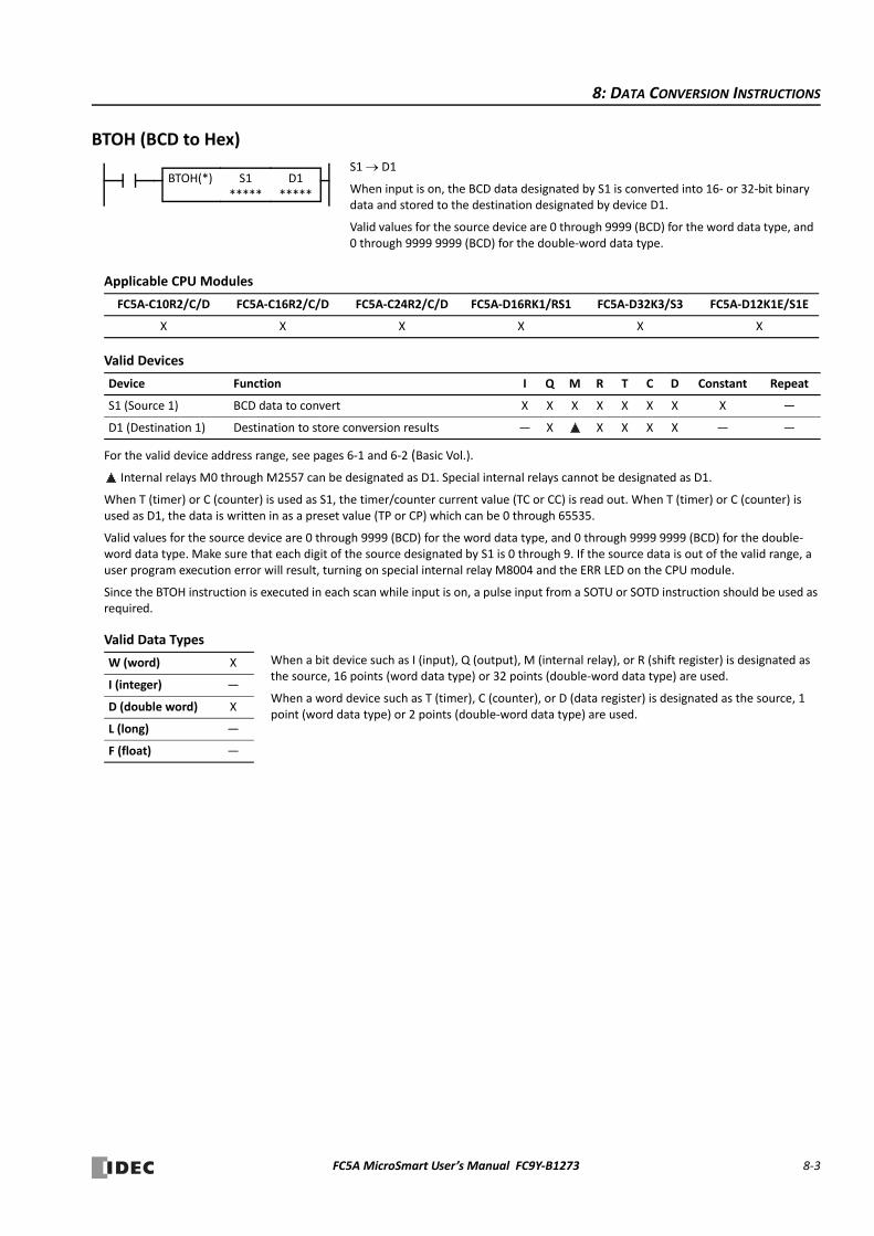
8: DATA CONVERSION INSTRUCTIONS
BTOH (BCD to Hex)
Applicable CPU Modules
Valid Devices
For the valid device address range, see pages 6‐1 and 6‐2 (Basic Vol.).
Internal relays M0 through M2557 can be designated as D1. Special internal relays cannot be designated as D1.
When T (timer) or C (counter) is used as S1, the timer/counter current value (TC or CC) is read out. When T (timer) or C (counter) is used as D1, the data is written in as a preset value (TP or CP) which can be 0 through 65535.
Valid values for the source device are 0 through 9999 (BCD) for the word data type, and 0 through 9999 9999 (BCD) for the double‐word data type. Make sure that each digit of the source designated by S1 is 0 through 9. If the source data is out of the valid range, a user program execution error will result, turning on special internal relay M8004 and the ERR LED on the CPU module.
Since the BTOH instruction is executed in each scan while input is on, a pulse input from a SOTU or SOTD instruction should be used as required.
Valid Data Types
FC5A‐C10R2/C/D FC5A‐C16R2/C/D FC5A‐C24R2/C/D FC5A‐D16RK1/RS1 FC5A‐D32K3/S3 FC5A‐D12K1E/S1E
X X X X X X
Device Function I Q M R T C D Constant Repeat
S1 (Source 1) BCD data to convert X X X X X X X X —
D1 (Destination 1) Destination to store conversion results — X X X X X — —
W (word) X
I (integer) —
D (double word) X
L (long) —
F (float) —
S1 D1
When input is on, the BCD data designated by S1 is converted into 16‐ or 32‐bit binary data and stored to the destination designated by device D1.
Valid values for the source device are 0 through 9999 (BCD) for the word data type, and 0 through 9999 9999 (BCD) for the double‐word data type.
BTOH(*) S1*****
D1*****
When a bit device such as I (input), Q (output), M (internal relay), or R (shift register) is designated as the source, 16 points (word data type) or 32 points (double‐word data type) are used.
When a word device such as T (timer), C (counter), or D (data register) is designated as the source, 1 point (word data type) or 2 points (double‐word data type) are used.
FC5A MicroSmart User’s Manual FC9Y‐B1273 8‐3
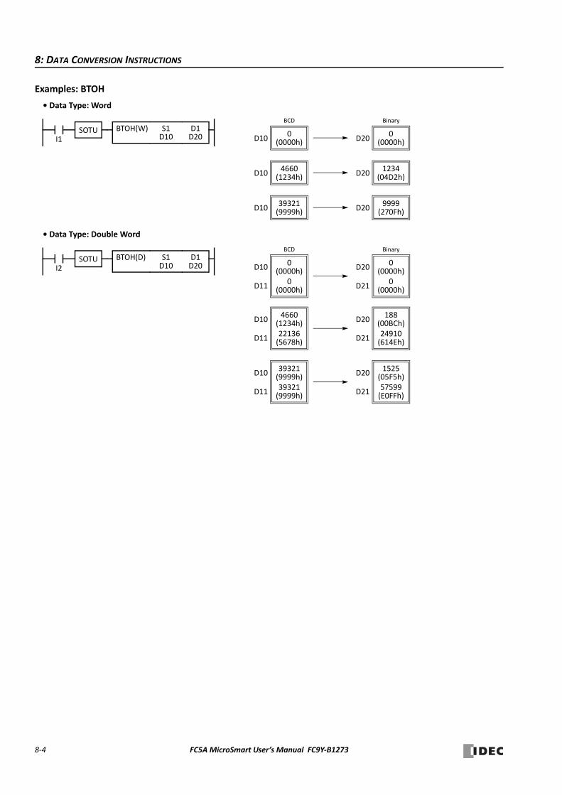
8: DATA CONVERSION INSTRUCTIONS
Examples: BTOH
• Data Type: Word
• Data Type: Double Word
D1D20
S1D10I1
BTOH(W)BCD
SOTU 0D10 (0000h)
Binary
0D20 (0000h)
4660D10 (1234h)
1234D20 (04D2h)
39321D10 (9999h)
9999D20 (270Fh)
D1D20
S1D10I2
BTOH(D)SOTU 0D10 (0000h)
0D11 (0000h)
0D20 (0000h)
0D21 (0000h)
BCD Binary
188D10 (00BCh)
24910D11 (614Eh)
4660D20(1234h)
22136D21(5678h)
1525D10 (05F5h)
57599D11 (E0FFh)
39321D20(9999h)
39321D21(9999h)
8‐4 FC5A MicroSmart User’s Manual FC9Y‐B1273

8: DATA CONVERSION INSTRUCTIONS
HTOA (Hex to ASCII)
Applicable CPU Modules
Valid Devices
For the valid device address range, see pages 6‐1 and 6‐2 (Basic Vol.).
When T (timer) or C (counter) is used as S1 or S2, the timer/counter current value (TC or CC) is read out.
The quantity of digits to convert can be 1 through 4. Make sure that the quantity of digits designated by S2 is within the valid range. If the S2 data is out of the valid range, a user program execution error will result, turning on special internal relay M8004 and the ERR LED on the CPU module.
Since the HTOA instruction is executed in each scan while input is on, a pulse input from a SOTU or SOTD instruction should be used as required.
Valid Data Types
FC5A‐C10R2/C/D FC5A‐C16R2/C/D FC5A‐C24R2/C/D FC5A‐D16RK1/RS1 FC5A‐D32K3/S3 FC5A‐D12K1E/S1E
X X X X X X
Device Function I Q M R T C D Constant Repeat
S1 (Source 1) Binary data to convert X X X X X X X X —
S2 (Source 2) Quantity of digits to convert X X X X X X X 1‐4 —
D1 (Destination 1) Destination to store conversion results — — — — — — X — —
W (word) X
I (integer) —
D (double word) —
L (long) —
F (float) —
S1 D1, D1+1, D1+2, D1+3
When input is on, the 16‐bit binary data designated by S1 is read from the lowest digit as many as the quantity of digits designated by S2, converted into ASCII data, and stored to the destination starting with the device designated by D1.
The quantity of digits to convert can be 1 through 4.
HTOA(W) S1*****
S2*****
D1*****
When a bit device such as I (input), Q (output), M (internal relay), or R (shift register) is designated as the source, 16 points (word data type) are used.
When a word device such as T (timer), C (counter), or D (data register) is designated as the source or destination, 1 point (word data type) is used.
FC5A MicroSmart User’s Manual FC9Y‐B1273 8‐5
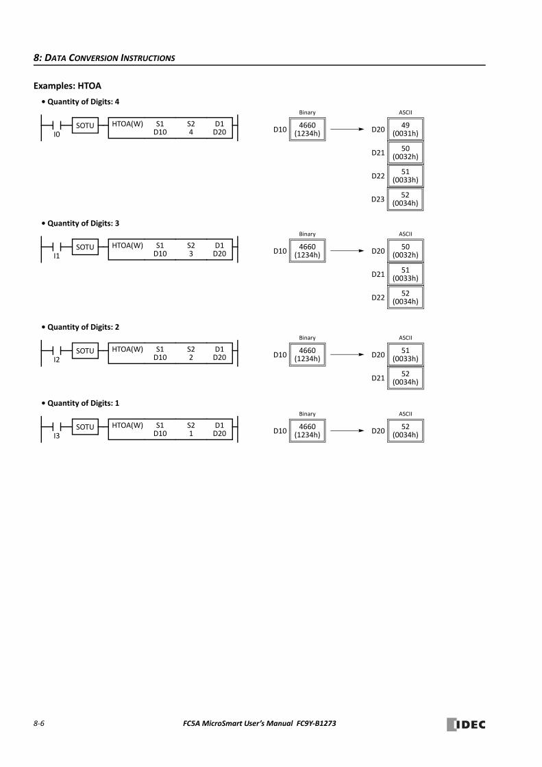
8: DATA CONVERSION INSTRUCTIONS
Examples: HTOA
• Quantity of Digits: 4
• Quantity of Digits: 3
• Quantity of Digits: 2
• Quantity of Digits: 1
D1D20
S1D10I0
HTOA(W) S24
SOTU
Binary
4660D10 (1234h)
ASCII
49D20 (0031h)
50D21 (0032h)
51D22 (0033h)
52D23 (0034h)
D1D20
S1D10I1
HTOA(W) S23
SOTU
Binary
4660D10 (1234h)
ASCII
50D20 (0032h)
51D21 (0033h)
52D22 (0034h)
D1D20
S1D10I2
HTOA(W) S22
SOTU
Binary
4660D10 (1234h)
ASCII
51D20 (0033h)
52D21 (0034h)
D1D20
S1D10I3
HTOA(W) S21
SOTU
Binary
4660D10 (1234h)
ASCII
52D20 (0034h)
8‐6 FC5A MicroSmart User’s Manual FC9Y‐B1273
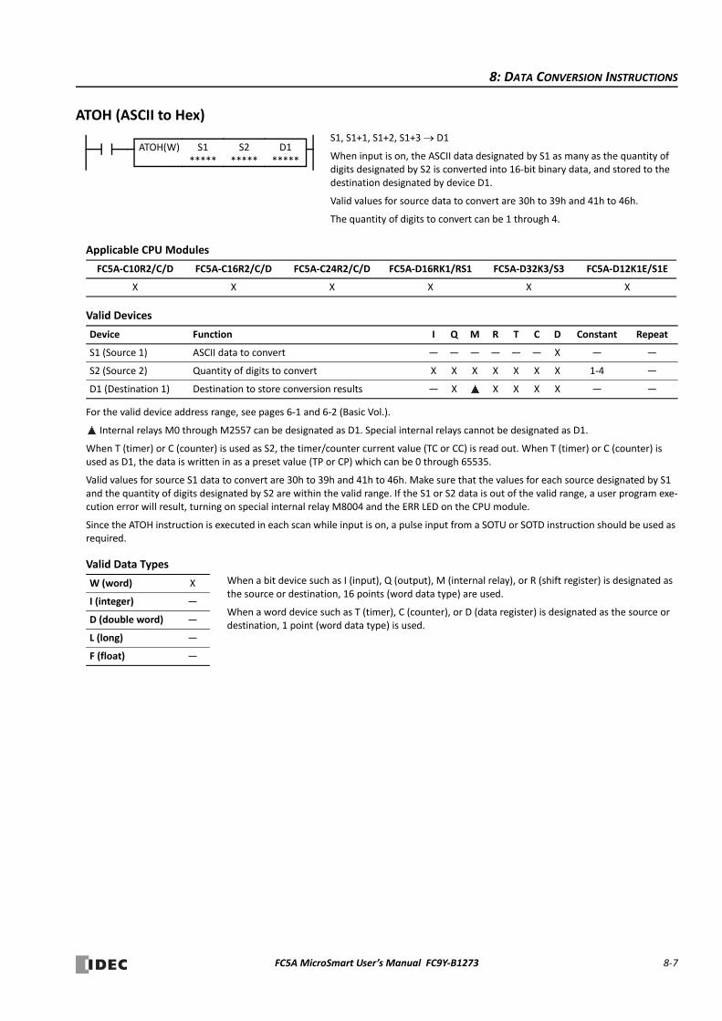
8: DATA CONVERSION INSTRUCTIONS
ATOH (ASCII to Hex)
Applicable CPU Modules
Valid Devices
For the valid device address range, see pages 6‐1 and 6‐2 (Basic Vol.).
Internal relays M0 through M2557 can be designated as D1. Special internal relays cannot be designated as D1.
When T (timer) or C (counter) is used as S2, the timer/counter current value (TC or CC) is read out. When T (timer) or C (counter) is used as D1, the data is written in as a preset value (TP or CP) which can be 0 through 65535.
Valid values for source S1 data to convert are 30h to 39h and 41h to 46h. Make sure that the values for each source designated by S1 and the quantity of digits designated by S2 are within the valid range. If the S1 or S2 data is out of the valid range, a user program exe‐cution error will result, turning on special internal relay M8004 and the ERR LED on the CPU module.
Since the ATOH instruction is executed in each scan while input is on, a pulse input from a SOTU or SOTD instruction should be used as required.
Valid Data Types
FC5A‐C10R2/C/D FC5A‐C16R2/C/D FC5A‐C24R2/C/D FC5A‐D16RK1/RS1 FC5A‐D32K3/S3 FC5A‐D12K1E/S1E
X X X X X X
Device Function I Q M R T C D Constant Repeat
S1 (Source 1) ASCII data to convert — — — — — — X — —
S2 (Source 2) Quantity of digits to convert X X X X X X X 1‐4 —
D1 (Destination 1) Destination to store conversion results — X X X X X — —
W (word) X
I (integer) —
D (double word) —
L (long) —
F (float) —
S1, S1+1, S1+2, S1+3 D1
When input is on, the ASCII data designated by S1 as many as the quantity of digits designated by S2 is converted into 16‐bit binary data, and stored to the destination designated by device D1.
Valid values for source data to convert are 30h to 39h and 41h to 46h.
The quantity of digits to convert can be 1 through 4.
ATOH(W) S1*****
S2*****
D1*****
When a bit device such as I (input), Q (output), M (internal relay), or R (shift register) is designated as the source or destination, 16 points (word data type) are used.
When a word device such as T (timer), C (counter), or D (data register) is designated as the source or destination, 1 point (word data type) is used.
FC5A MicroSmart User’s Manual FC9Y‐B1273 8‐7

8: DATA CONVERSION INSTRUCTIONS
Examples: ATOH
• Quantity of Digits: 4
• Quantity of Digits: 3
• Quantity of Digits: 2
• Quantity of Digits: 1
D1D20
S1D10I0
ATOH(W) S24
SOTU
Binary
4660D20 (1234h)
ASCII
49D10 (0031h)
50D11 (0032h)
51D12 (0033h)
52D13 (0034h)
D1D20
S1D10I1
ATOH(W) S23
SOTU
Binary
291D20 (0123h)
ASCII
49D10 (0031h)
50D11 (0032h)
51D12 (0033h)
D1D20
S1D10I2
ATOH(W) S22
SOTU
Binary
18D20 (0012h)
ASCII
49D10 (0031h)
50D11 (0032h)
D1D20
S1D10I3
ATOH(W) S21
SOTU
Binary
1D20 (0001h)
ASCII
49D10 (0031h)
8‐8 FC5A MicroSmart User’s Manual FC9Y‐B1273
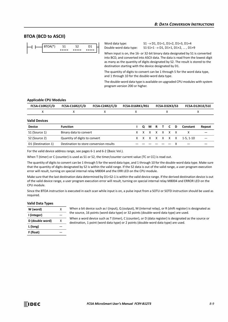
8: DATA CONVERSION INSTRUCTIONS
BTOA (BCD to ASCII)
Applicable CPU Modules
Valid Devices
For the valid device address range, see pages 6‐1 and 6‐2 (Basic Vol.).
When T (timer) or C (counter) is used as S1 or S2, the timer/counter current value (TC or CC) is read out.
The quantity of digits to convert can be 1 through 5 for the word data type, and 1 through 10 for the double‐word data type. Make sure that the quantity of digits designated by S2 is within the valid range. If the S2 data is out of the valid range, a user program execution error will result, turning on special internal relay M8004 and the ERR LED on the CPU module.
Make sure that the last destination data determined by D1+S2‐1 is within the valid device range. If the derived destination device is out of the valid device range, a user program execution error will result, turning on special internal relay M8004 and ERROR LED on the CPU module.
Since the BTOA instruction is executed in each scan while input is on, a pulse input from a SOTU or SOTD instruction should be used as required.
Valid Data Types
FC5A‐C10R2/C/D FC5A‐C16R2/C/D FC5A‐C24R2/C/D FC5A‐D16RK1/RS1 FC5A‐D32K3/S3 FC5A‐D12K1E/S1E
X X X X X X
Device Function I Q M R T C D Constant Repeat
S1 (Source 1) Binary data to convert X X X X X X X X —
S2 (Source 2) Quantity of digits to convert X X X X X X X 1‐5, 1‐10 —
D1 (Destination 1) Destination to store conversion results — — — — — — X — —
W (word) X
I (integer) —
D (double word) X
L (long) —
F (float) —
Word data type: S1 D1, D1+1, D1+2, D1+3, D1+4Double‐word data type: S1∙S1+1 D1, D1+1, D1+2, ... , D1+9
When input is on, the 16‐ or 32‐bit binary data designated by S1 is converted into BCD, and converted into ASCII data. The data is read from the lowest digit as many as the quantity of digits designated by S2. The result is stored to the destination starting with the device designated by D1.
The quantity of digits to convert can be 1 through 5 for the word data type, and 1 through 10 for the double‐word data type.
The double‐word data type is available on upgraded CPU modules with system program version 200 or higher.
BTOA(*)
S1*****
S2*****
D1*****
When a bit device such as I (input), Q (output), M (internal relay), or R (shift register) is designated as the source, 16 points (word data type) or 32 points (double‐word data type) are used.
When a word device such as T (timer), C (counter), or D (data register) is designated as the source or destination, 1 point (word data type) or 2 points (double‐word data type) are used.
FC5A MicroSmart User’s Manual FC9Y‐B1273 8‐9
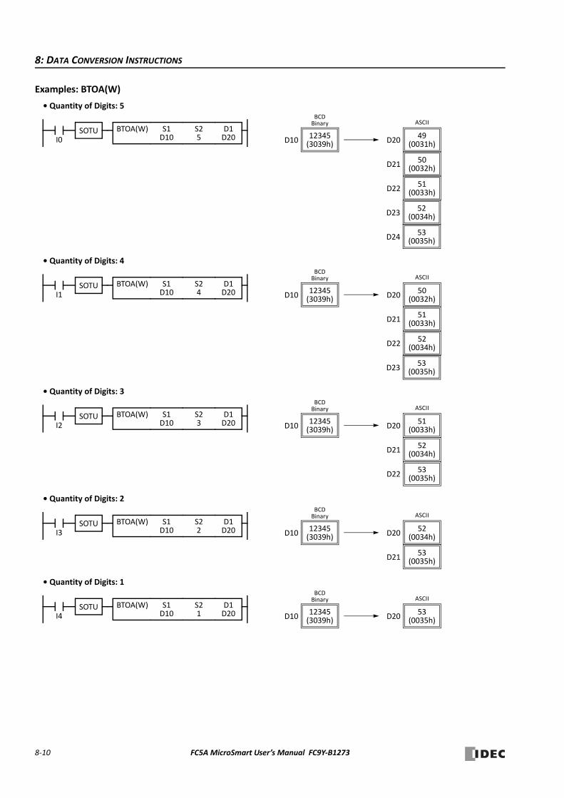
8: DATA CONVERSION INSTRUCTIONS
Examples: BTOA(W)
• Quantity of Digits: 5
• Quantity of Digits: 4
• Quantity of Digits: 3
• Quantity of Digits: 2
• Quantity of Digits: 1
D1D20
S1D10I0
BTOA(W) S25
SOTU
BCD
12345D10 (3039h)
ASCII
49D20 (0031h)
50D21 (0032h)
51D22 (0033h)
52D23 (0034h)
Binary
53D24 (0035h)
D1D20
S1D10I1
BTOA(W) S24
SOTU
BCD
12345D10 (3039h)
ASCII
50D20 (0032h)
51D21 (0033h)
52D22 (0034h)
53D23 (0035h)
Binary
D1D20
S1D10I2
BTOA(W) S23
SOTU
BCD
12345D10 (3039h)
ASCII
51D20 (0033h)
52D21 (0034h)
53D22 (0035h)
Binary
D1D20
S1D10I3
BTOA(W) S22
SOTU
BCD
12345D10 (3039h)
ASCII
52D20 (0034h)
53D21 (0035h)
Binary
D1D20
S1D10I4
BTOA(W) S21
SOTU
BCD
12345D10 (3039h)
ASCII
53D20 (0035h)
Binary
8‐10 FC5A MicroSmart User’s Manual FC9Y‐B1273
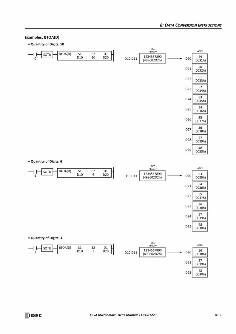
8: DATA CONVERSION INSTRUCTIONS
Examples: BTOA(D)
• Quantity of Digits: 10
• Quantity of Digits: 6
• Quantity of Digits: 3
D1D20
S1D10I0
BTOA(D)
S210
SOTU
BCD
1234567890(499602D2h)
ASCII
49D20 (0031h)
50D21 (0032h)
51D22 (0033h)
52D23 (0034h)
Binary
53D24 (0035h)
54D25 (0036h)
55D26 (0037h)
56D27 (0038h)
57D28 (0039h)
48D29 (0030h)
D10∙D11
D1D20
S1D10I1
BTOA(D)
S26
SOTUASCII
53D20 (0035h)
54D21 (0036h)
55D22 (0037h)
56D23 (0038h)
57D24 (0039h)
48D25 (0030h)
BCDBinary
D10∙D111234567890(499602D2h)
D1D20
S1D10I2
BTOA(D)
S23
SOTUASCII
56D20 (0038h)
57D21 (0039h)
48D22 (0030h)
BCDBinary
D10∙D111234567890(499602D2h)
FC5A MicroSmart User’s Manual FC9Y‐B1273 8‐11
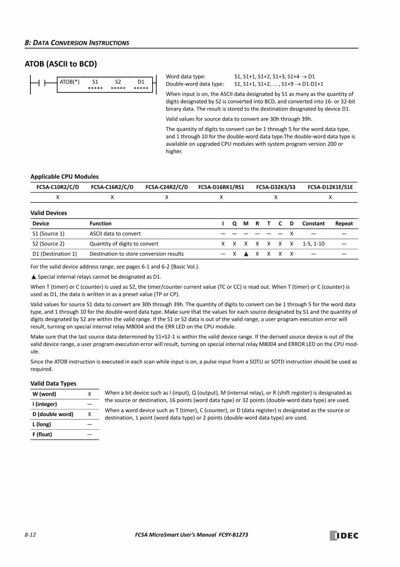
8: DATA CONVERSION INSTRUCTIONS
ATOB (ASCII to BCD)
Applicable CPU Modules
Valid Devices
For the valid device address range, see pages 6‐1 and 6‐2 (Basic Vol.).
Special internal relays cannot be designated as D1.
When T (timer) or C (counter) is used as S2, the timer/counter current value (TC or CC) is read out. When T (timer) or C (counter) is used as D1, the data is written in as a preset value (TP or CP).
Valid values for source S1 data to convert are 30h through 39h. The quantity of digits to convert can be 1 through 5 for the word data type, and 1 through 10 for the double‐word data type. Make sure that the values for each source designated by S1 and the quantity of digits designated by S2 are within the valid range. If the S1 or S2 data is out of the valid range, a user program execution error will result, turning on special internal relay M8004 and the ERR LED on the CPU module.
Make sure that the last source data determined by S1+S2‐1 is within the valid device range. If the derived source device is out of the valid device range, a user program execution error will result, turning on special internal relay M8004 and ERROR LED on the CPU mod‐ule.
Since the ATOB instruction is executed in each scan while input is on, a pulse input from a SOTU or SOTD instruction should be used as required.
Valid Data Types
FC5A‐C10R2/C/D FC5A‐C16R2/C/D FC5A‐C24R2/C/D FC5A‐D16RK1/RS1 FC5A‐D32K3/S3 FC5A‐D12K1E/S1E
X X X X X X
Device Function I Q M R T C D Constant Repeat
S1 (Source 1) ASCII data to convert — — — — — — X — —
S2 (Source 2) Quantity of digits to convert X X X X X X X 1‐5, 1‐10 —
D1 (Destination 1) Destination to store conversion results — X X X X X — —
W (word) X
I (integer) —
D (double word) X
L (long) —
F (float) —
Word data type: S1, S1+1, S1+2, S1+3, S1+4 D1Double‐word data type: S1, S1+1, S1+2, ... , S1+9 D1∙D1+1
When input is on, the ASCII data designated by S1 as many as the quantity of digits designated by S2 is converted into BCD, and converted into 16‐ or 32‐bit binary data. The result is stored to the destination designated by device D1.
Valid values for source data to convert are 30h through 39h.
The quantity of digits to convert can be 1 through 5 for the word data type, and 1 through 10 for the double‐word data type.The double‐word data type is available on upgraded CPU modules with system program version 200 or higher.
ATOB(*)
S1*****
S2*****
D1*****
When a bit device such as I (input), Q (output), M (internal relay), or R (shift register) is designated as the source or destination, 16 points (word data type) or 32 points (double‐word data type) are used.
When a word device such as T (timer), C (counter), or D (data register) is designated as the source or destination, 1 point (word data type) or 2 points (double‐word data type) are used.
8‐12 FC5A MicroSmart User’s Manual FC9Y‐B1273

8: DATA CONVERSION INSTRUCTIONS
Examples: ATOB(W)
• Quantity of Digits: 5
• Quantity of Digits: 4
• Quantity of Digits: 3
• Quantity of Digits: 2
• Quantity of Digits: 1
D1D20
S1D10I0
ATOB(W) S25
SOTU
BCD
12345D20 (3039h)
ASCII
49D10 (0031h)
50D11 (0032h)
51D12 (0033h)
52D13 (0034h)
Binary
53D14 (0035h)
D1D20
S1D10I1
ATOB(W) S24
SOTU
BCD
1234D20 (04D2h)
ASCII
49D10 (0031h)
50D11 (0032h)
51D12 (0033h)
52D13 (0034h)
Binary
D1D20
S1D10I2
ATOB(W) S23
SOTU
BCD
123D20 (007Bh)
ASCII
49D10 (0031h)
50D11 (0032h)
51D12 (0033h)
Binary
D1D20
S1D10I3
ATOB(W) S22
SOTU
BCD
12D20 (0018h)
ASCII
49D10 (0031h)
50D11 (0032h)
Binary
D1D20
S1D10I4
ATOB(W) S21
SOTU
BCD
1D20 (0001h)
ASCII
49D10 (0031h)
Binary
FC5A MicroSmart User’s Manual FC9Y‐B1273 8‐13

8: DATA CONVERSION INSTRUCTIONS
Examples: ATOB(D)
• Quantity of Digits: 10
• Quantity of Digits: 6
• Quantity of Digits: 3
D1D20
S1D10I0
ATOB(D)
S210
SOTUASCII
49D10 (0031h)
50D11 (0032h)
51D12 (0033h)
52D13 (0034h)
53D14 (0035h)
54D15 (0036h)
55D16 (0037h)
56D17 (0038h)
57D18 (0039h)
48D19 (0030h)
BCD
1234567890(499602D2h)
Binary
D20∙D21
D1D20
S1D10I1
ATOB(D)
S26
SOTU
BCD
123456(0001E240h)
ASCII
49D10 (0031h)
50D11 (0032h)
51D12 (0033h)
52D13 (0034h)
Binary
53D14 (0035h)
54D15 (0036h)
D20∙D21
D1D20
S1D10I2
ATOB(D)
S23
SOTU
BCD
123(0000007Bh)
ASCII
49D10 (0031h)
50D11 (0032h)
51D12 (0033h)
Binary
D20∙D21
8‐14 FC5A MicroSmart User’s Manual FC9Y‐B1273
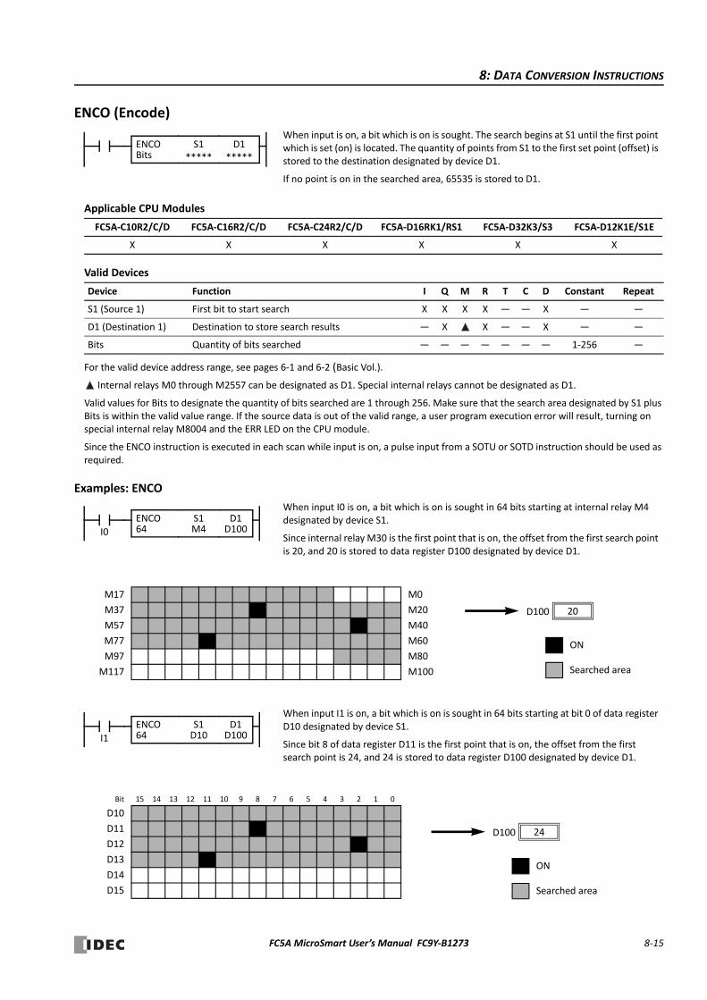
8: DATA CONVERSION INSTRUCTIONS
ENCO (Encode)
Applicable CPU Modules
Valid Devices
For the valid device address range, see pages 6‐1 and 6‐2 (Basic Vol.).
Internal relays M0 through M2557 can be designated as D1. Special internal relays cannot be designated as D1.
Valid values for Bits to designate the quantity of bits searched are 1 through 256. Make sure that the search area designated by S1 plus Bits is within the valid value range. If the source data is out of the valid range, a user program execution error will result, turning on special internal relay M8004 and the ERR LED on the CPU module.
Since the ENCO instruction is executed in each scan while input is on, a pulse input from a SOTU or SOTD instruction should be used as required.
Examples: ENCO
FC5A‐C10R2/C/D FC5A‐C16R2/C/D FC5A‐C24R2/C/D FC5A‐D16RK1/RS1 FC5A‐D32K3/S3 FC5A‐D12K1E/S1E
X X X X X X
Device Function I Q M R T C D Constant Repeat
S1 (Source 1) First bit to start search X X X X — — X — —
D1 (Destination 1) Destination to store search results — X X — — X — —
Bits Quantity of bits searched — — — — — — — 1‐256 —
When input is on, a bit which is on is sought. The search begins at S1 until the first point which is set (on) is located. The quantity of points from S1 to the first set point (offset) is stored to the destination designated by device D1.
If no point is on in the searched area, 65535 is stored to D1.
ENCOBits
S1*****
D1*****
D1D100
S1M4I0
ENCO64
M17 M0
M37 M20
M57 M40
M77 M60
M97 M80
M117 M100
When input I0 is on, a bit which is on is sought in 64 bits starting at internal relay M4 designated by device S1.
Since internal relay M30 is the first point that is on, the offset from the first search point is 20, and 20 is stored to data register D100 designated by device D1.
ON
Searched area
20D100
D1D100
S1D10I1
ENCO64
Bit 15 14 13 12 11 10 9 8 7 6 5 4 3 2 1 0
D10
D11
D12
D13
D14
D15
When input I1 is on, a bit which is on is sought in 64 bits starting at bit 0 of data register D10 designated by device S1.
Since bit 8 of data register D11 is the first point that is on, the offset from the first search point is 24, and 24 is stored to data register D100 designated by device D1.
ON
Searched area
24D100
FC5A MicroSmart User’s Manual FC9Y‐B1273 8‐15

8: DATA CONVERSION INSTRUCTIONS
DECO (Decode)
Applicable CPU Modules
Valid Devices
For the valid device address range, see pages 6‐1 and 6‐2 (Basic Vol.).
Internal relays M0 through M2557 can be designated as D1. Special internal relays cannot be designated as D1.
Valid values for the offset designated by source device S1 are 0 through 255. Make sure that the offset designated by S1 and the last bit of destination data determined by the sum of S1 and D1 are within the valid value range. If the offset or destination data is out of the valid range, a user program execution error will result, turning on special internal relay M8004 and the ERR LED on the CPU module.
Since the DECO instruction is executed in each scan while input is on, a pulse input from a SOTU or SOTD instruction should be used as required.
Examples: DECO
FC5A‐C10R2/C/D FC5A‐C16R2/C/D FC5A‐C24R2/C/D FC5A‐D16RK1/RS1 FC5A‐D32K3/S3 FC5A‐D12K1E/S1E
X X X X X X
Device Function I Q M R T C D Constant Repeat
S1 (Source 1) Offset X X X X — — X 0‐255 —
D1 (Destination 1) First bit to count offset — X X — — X — —
When input is on, the values contained in devices designated by S1 and D1 are added to determine the destination, and the bit so determined is turned on.DECO S1
*****D1
*****
D1M104
S1D20I0
DECO
M117 M100
M137 M120
M157 M140
M177 M160
M197 M180
M217 M200
When input I0 is on, the destination bit is determined by adding the value contained in data register D20 designated by device S1 to internal relay M104 designated by destina‐tion device D1.
Since 19th bit from internal relay M104 is internal relay M127, the bit so determined is turned on.
19D20
First bit
ON
D1D30
S1D10I1
DECO
Bit 15 14 13 12 11 10 9 8 7 6 5 4 3 2 1 0
D30
D31
D32
D33
D34
D35
When input I1 is on, the destination bit is determined by adding the value contained in data register D10 designated by device S1 to data register D30 designated by destination device D1.
Since 39th bit from data register D30 bit 0 is data register D32 bit 7, the bit so deter‐mined is turned on.
ON
39D10
8‐16 FC5A MicroSmart User’s Manual FC9Y‐B1273
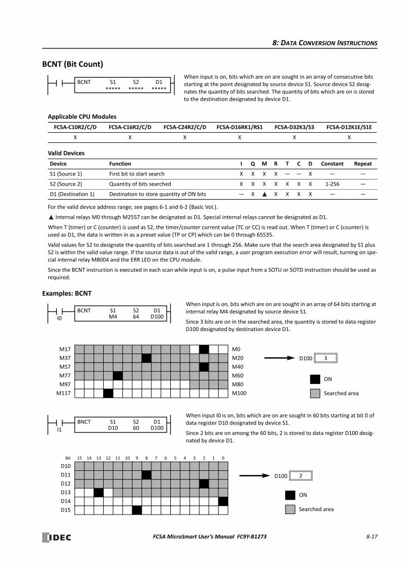
8: DATA CONVERSION INSTRUCTIONS
BCNT (Bit Count)
Applicable CPU Modules
Valid Devices
For the valid device address range, see pages 6‐1 and 6‐2 (Basic Vol.).
Internal relays M0 through M2557 can be designated as D1. Special internal relays cannot be designated as D1.
When T (timer) or C (counter) is used as S2, the timer/counter current value (TC or CC) is read out. When T (timer) or C (counter) is used as D1, the data is written in as a preset value (TP or CP) which can be 0 through 65535.
Valid values for S2 to designate the quantity of bits searched are 1 through 256. Make sure that the search area designated by S1 plus S2 is within the valid value range. If the source data is out of the valid range, a user program execution error will result, turning on spe‐cial internal relay M8004 and the ERR LED on the CPU module.
Since the BCNT instruction is executed in each scan while input is on, a pulse input from a SOTU or SOTD instruction should be used as required.
Examples: BCNT
FC5A‐C10R2/C/D FC5A‐C16R2/C/D FC5A‐C24R2/C/D FC5A‐D16RK1/RS1 FC5A‐D32K3/S3 FC5A‐D12K1E/S1E
X X X X X X
Device Function I Q M R T C D Constant Repeat
S1 (Source 1) First bit to start search X X X X — — X — —
S2 (Source 2) Quantity of bits searched X X X X X X X 1‐256 —
D1 (Destination 1) Destination to store quantity of ON bits — X X X X X — —
When input is on, bits which are on are sought in an array of consecutive bits starting at the point designated by source device S1. Source device S2 desig‐nates the quantity of bits searched. The quantity of bits which are on is stored to the destination designated by device D1.
BCNT S1*****
D1*****
S2*****
D1D100
S1M4I0
BCNT
M17 M0
M37 M20
M57 M40
M77 M60
M97 M80
M117 M100
ON
Searched area
3D100
S264
When input is on, bits which are on are sought in an array of 64 bits starting at internal relay M4 designated by source device S1.
Since 3 bits are on in the searched area, the quantity is stored to data register D100 designated by destination device D1.
D1D100
S1D10I1
BNCT
Bit 15 14 13 12 11 10 9 8 7 6 5 4 3 2 1 0
D10
D11
D12
D13
D14
D15
When input I0 is on, bits which are on are sought in 60 bits starting at bit 0 of data register D10 designated by device S1.
Since 2 bits are on among the 60 bits, 2 is stored to data register D100 desig‐nated by device D1.
ON
Searched area
2D100
S260
FC5A MicroSmart User’s Manual FC9Y‐B1273 8‐17
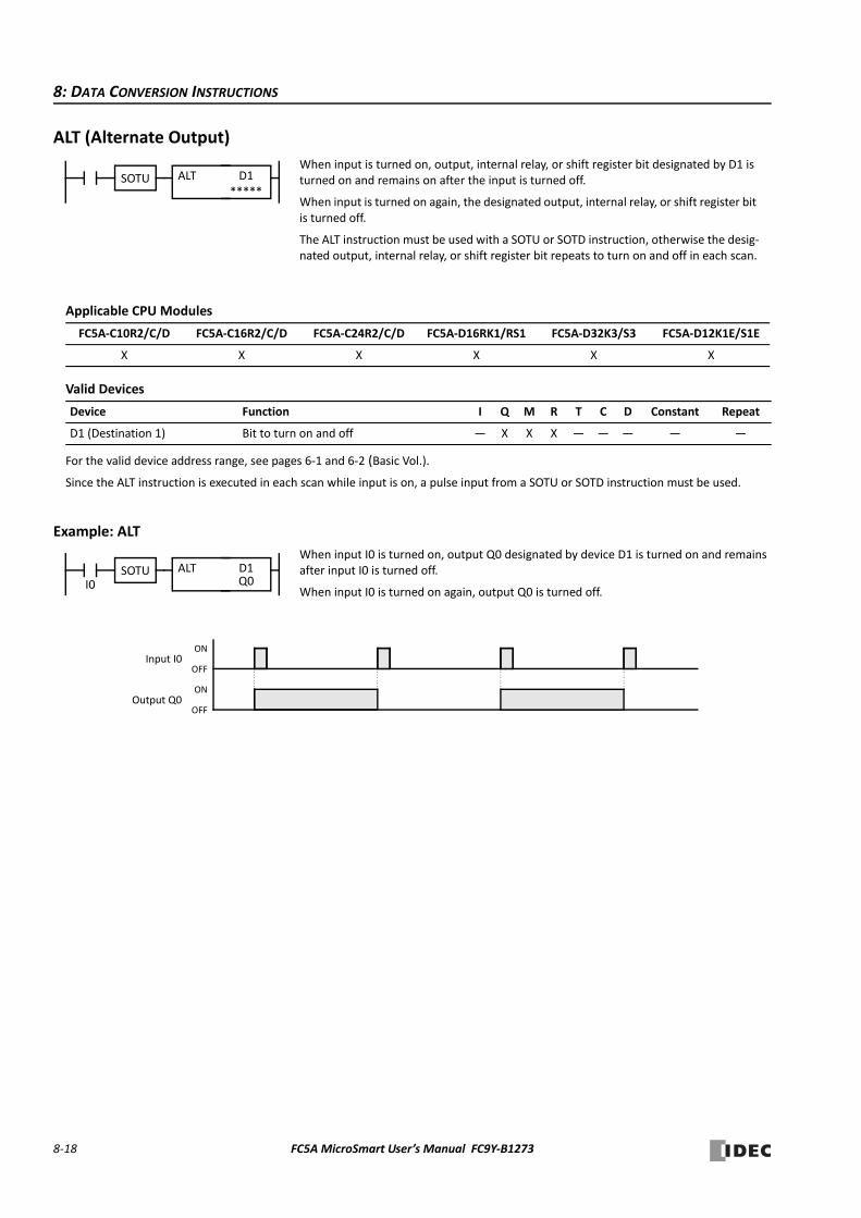
8: DATA CONVERSION INSTRUCTIONS
ALT (Alternate Output)
Applicable CPU Modules
Valid Devices
For the valid device address range, see pages 6‐1 and 6‐2 (Basic Vol.).
Since the ALT instruction is executed in each scan while input is on, a pulse input from a SOTU or SOTD instruction must be used.
Example: ALT
FC5A‐C10R2/C/D FC5A‐C16R2/C/D FC5A‐C24R2/C/D FC5A‐D16RK1/RS1 FC5A‐D32K3/S3 FC5A‐D12K1E/S1E
X X X X X X
Device Function I Q M R T C D Constant Repeat
D1 (Destination 1) Bit to turn on and off — X X X — — — — —
When input is turned on, output, internal relay, or shift register bit designated by D1 is turned on and remains on after the input is turned off.
When input is turned on again, the designated output, internal relay, or shift register bit is turned off.
The ALT instruction must be used with a SOTU or SOTD instruction, otherwise the desig‐nated output, internal relay, or shift register bit repeats to turn on and off in each scan.
ALT D1*****
SOTU
D1Q0I0
ALTWhen input I0 is turned on, output Q0 designated by device D1 is turned on and remains after input I0 is turned off.
When input I0 is turned on again, output Q0 is turned off.
SOTU
Input I0
Output Q0
ON
OFF
ON
OFF
8‐18 FC5A MicroSmart User’s Manual FC9Y‐B1273
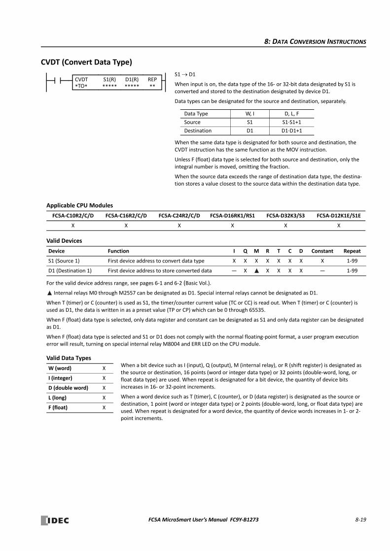
8: DATA CONVERSION INSTRUCTIONS
CVDT (Convert Data Type)
Applicable CPU Modules
Valid Devices
For the valid device address range, see pages 6‐1 and 6‐2 (Basic Vol.).
Internal relays M0 through M2557 can be designated as D1. Special internal relays cannot be designated as D1.
When T (timer) or C (counter) is used as S1, the timer/counter current value (TC or CC) is read out. When T (timer) or C (counter) is used as D1, the data is written in as a preset value (TP or CP) which can be 0 through 65535.
When F (float) data type is selected, only data register and constant can be designated as S1 and only data register can be designated as D1.
When F (float) data type is selected and S1 or D1 does not comply with the normal floating‐point format, a user program execution error will result, turning on special internal relay M8004 and ERR LED on the CPU module.
Valid Data Types
FC5A‐C10R2/C/D FC5A‐C16R2/C/D FC5A‐C24R2/C/D FC5A‐D16RK1/RS1 FC5A‐D32K3/S3 FC5A‐D12K1E/S1E
X X X X X X
Device Function I Q M R T C D Constant Repeat
S1 (Source 1) First device address to convert data type X X X X X X X X 1‐99
D1 (Destination 1) First device address to store converted data — X X X X X — 1‐99
W (word) X
I (integer) X
D (double word) X
L (long) X
F (float) X
S1 D1
When input is on, the data type of the 16‐ or 32‐bit data designated by S1 is converted and stored to the destination designated by device D1.
Data types can be designated for the source and destination, separately.
When the same data type is designated for both source and destination, the CVDT instruction has the same function as the MOV instruction.
Unless F (float) data type is selected for both source and destination, only the integral number is moved, omitting the fraction.
When the source data exceeds the range of destination data type, the destina‐tion stores a value closest to the source data within the destination data type.
Data Type W, I D, L, F
Source S1 S1∙S1+1
Destination D1 D1∙D1+1
S1(R)*****
REP**
D1(R)*****
CVDT*TO*
When a bit device such as I (input), Q (output), M (internal relay), or R (shift register) is designated as the source or destination, 16 points (word or integer data type) or 32 points (double‐word, long, or float data type) are used. When repeat is designated for a bit device, the quantity of device bits increases in 16‐ or 32‐point increments.
When a word device such as T (timer), C (counter), or D (data register) is designated as the source or destination, 1 point (word or integer data type) or 2 points (double‐word, long, or float data type) are used. When repeat is designated for a word device, the quantity of device words increases in 1‐ or 2‐point increments.
FC5A MicroSmart User’s Manual FC9Y‐B1273 8‐19
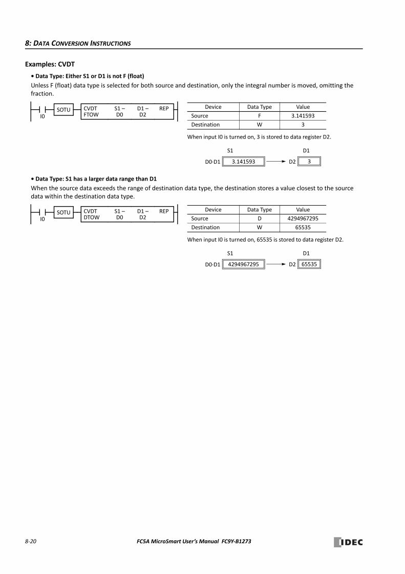
8: DATA CONVERSION INSTRUCTIONS
Examples: CVDT
• Data Type: Either S1 or D1 is not F (float)
Unless F (float) data type is selected for both source and destination, only the integral number is moved, omitting the fraction.
• Data Type: S1 has a larger data range than D1
When the source data exceeds the range of destination data type, the destination stores a value closest to the source data within the destination data type.
I0
REPD1 –D2
SOTU
When input I0 is turned on, 3 is stored to data register D2.
Device Data Type Value
Source F 3.141593
Destination W 3
S1 –D0
CVDTFTOW
3D2
D1S1
3.141593D0∙D1
I0
REPD1 –D2
SOTU
When input I0 is turned on, 65535 is stored to data register D2.
Device Data Type Value
Source D 4294967295
Destination W 65535
S1 –D0
CVDTDTOW
65535D2
D1S1
4294967295D0∙D1
8‐20 FC5A MicroSmart User’s Manual FC9Y‐B1273
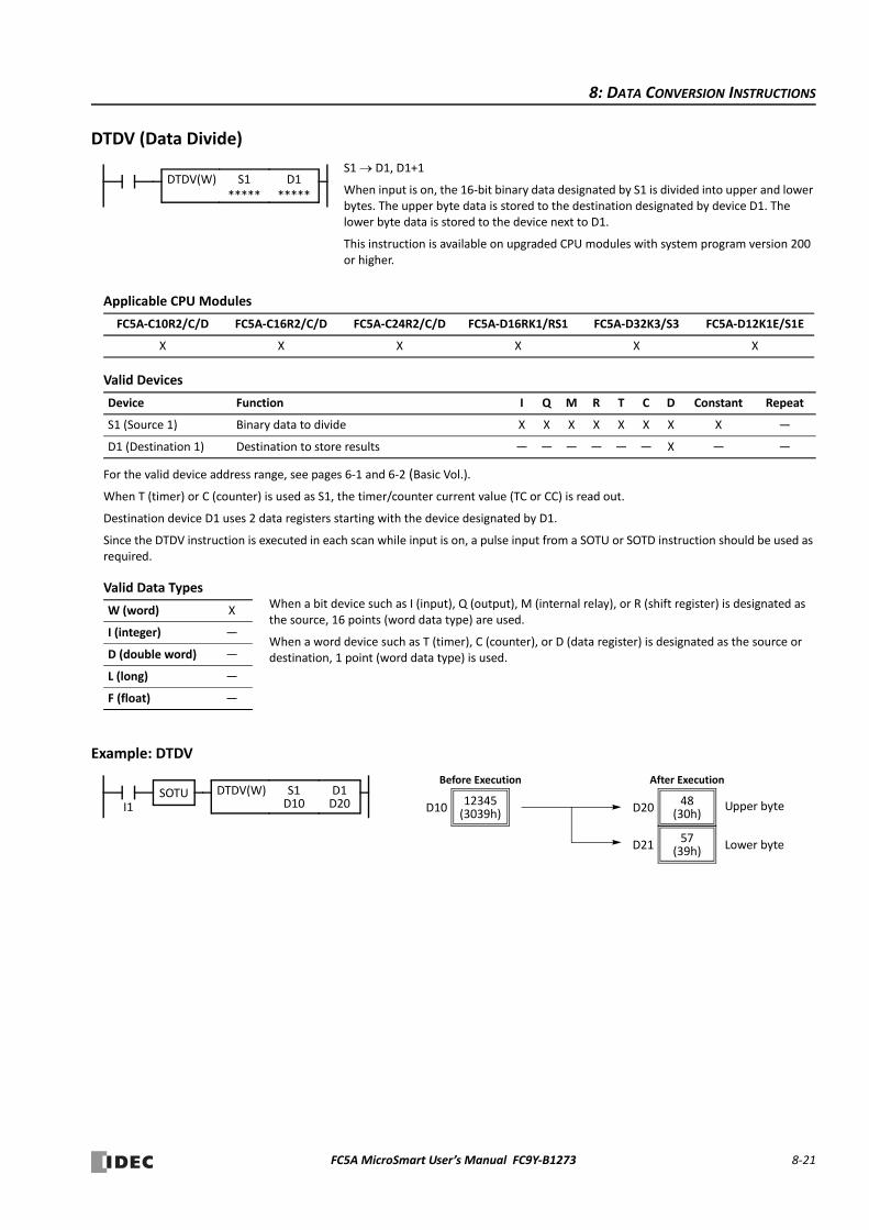
8: DATA CONVERSION INSTRUCTIONS
DTDV (Data Divide)
Applicable CPU Modules
Valid Devices
For the valid device address range, see pages 6‐1 and 6‐2 (Basic Vol.).
When T (timer) or C (counter) is used as S1, the timer/counter current value (TC or CC) is read out.
Destination device D1 uses 2 data registers starting with the device designated by D1.
Since the DTDV instruction is executed in each scan while input is on, a pulse input from a SOTU or SOTD instruction should be used as required.
Valid Data Types
Example: DTDV
FC5A‐C10R2/C/D FC5A‐C16R2/C/D FC5A‐C24R2/C/D FC5A‐D16RK1/RS1 FC5A‐D32K3/S3 FC5A‐D12K1E/S1E
X X X X X X
Device Function I Q M R T C D Constant Repeat
S1 (Source 1) Binary data to divide X X X X X X X X —
D1 (Destination 1) Destination to store results — — — — — — X — —
W (word) X
I (integer) —
D (double word) —
L (long) —
F (float) —
S1 D1, D1+1
When input is on, the 16‐bit binary data designated by S1 is divided into upper and lower bytes. The upper byte data is stored to the destination designated by device D1. The lower byte data is stored to the device next to D1.
This instruction is available on upgraded CPU modules with system program version 200 or higher.
DTDV(W)
S1*****
D1*****
When a bit device such as I (input), Q (output), M (internal relay), or R (shift register) is designated as the source, 16 points (word data type) are used.
When a word device such as T (timer), C (counter), or D (data register) is designated as the source or destination, 1 point (word data type) is used.
D1D20
S1D10I1
DTDV(W)
SOTU48
D20 (30h)
Before Execution
12345D10 (3039h)
After Execution
57D21 (39h)
Upper byte
Lower byte
FC5A MicroSmart User’s Manual FC9Y‐B1273 8‐21
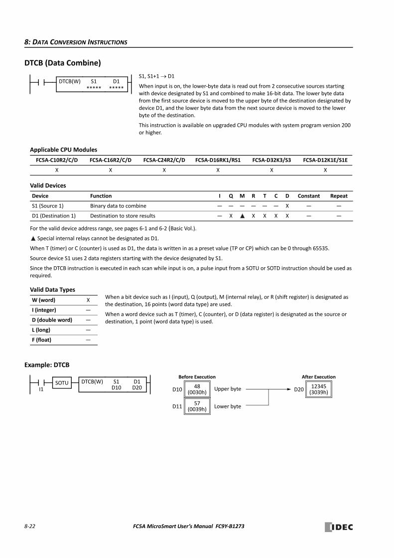
8: DATA CONVERSION INSTRUCTIONS
DTCB (Data Combine)
Applicable CPU Modules
Valid Devices
For the valid device address range, see pages 6‐1 and 6‐2 (Basic Vol.).
Special internal relays cannot be designated as D1.
When T (timer) or C (counter) is used as D1, the data is written in as a preset value (TP or CP) which can be 0 through 65535.
Source device S1 uses 2 data registers starting with the device designated by S1.
Since the DTCB instruction is executed in each scan while input is on, a pulse input from a SOTU or SOTD instruction should be used as required.
Valid Data Types
Example: DTCB
FC5A‐C10R2/C/D FC5A‐C16R2/C/D FC5A‐C24R2/C/D FC5A‐D16RK1/RS1 FC5A‐D32K3/S3 FC5A‐D12K1E/S1E
X X X X X X
Device Function I Q M R T C D Constant Repeat
S1 (Source 1) Binary data to combine — — — — — — X — —
D1 (Destination 1) Destination to store results — X X X X X — —
W (word) X
I (integer) —
D (double word) —
L (long) —
F (float) —
S1, S1+1 D1
When input is on, the lower‐byte data is read out from 2 consecutive sources starting with device designated by S1 and combined to make 16‐bit data. The lower byte data from the first source device is moved to the upper byte of the destination designated by device D1, and the lower byte data from the next source device is moved to the lower byte of the destination.
This instruction is available on upgraded CPU modules with system program version 200 or higher.
DTCB(W)
S1*****
D1*****
When a bit device such as I (input), Q (output), M (internal relay), or R (shift register) is designated as the destination, 16 points (word data type) are used.
When a word device such as T (timer), C (counter), or D (data register) is designated as the source or destination, 1 point (word data type) is used.
D1D20
S1D10I1
DTCB(W)
SOTU48
D10 (0030h)
After Execution
12345D20 (3039h)
Before Execution
57D11 (0039h)
Upper byte
Lower byte
8‐22 FC5A MicroSmart User’s Manual FC9Y‐B1273
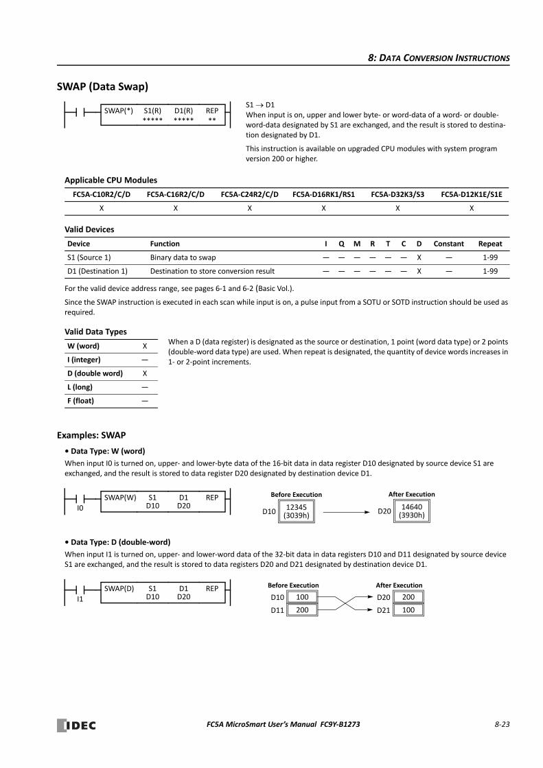
8: DATA CONVERSION INSTRUCTIONS
SWAP (Data Swap)
Applicable CPU Modules
Valid Devices
For the valid device address range, see pages 6‐1 and 6‐2 (Basic Vol.).
Since the SWAP instruction is executed in each scan while input is on, a pulse input from a SOTU or SOTD instruction should be used as required.
Valid Data Types
Examples: SWAP
• Data Type: W (word)
When input I0 is turned on, upper‐ and lower‐byte data of the 16‐bit data in data register D10 designated by source device S1 are exchanged, and the result is stored to data register D20 designated by destination device D1.
• Data Type: D (double‐word)
When input I1 is turned on, upper‐ and lower‐word data of the 32‐bit data in data registers D10 and D11 designated by source device S1 are exchanged, and the result is stored to data registers D20 and D21 designated by destination device D1.
FC5A‐C10R2/C/D FC5A‐C16R2/C/D FC5A‐C24R2/C/D FC5A‐D16RK1/RS1 FC5A‐D32K3/S3 FC5A‐D12K1E/S1E
X X X X X X
Device Function I Q M R T C D Constant Repeat
S1 (Source 1) Binary data to swap — — — — — — X — 1‐99
D1 (Destination 1) Destination to store conversion result — — — — — — X — 1‐99
W (word) X
I (integer) —
D (double word) X
L (long) —
F (float) —
S1 D1When input is on, upper and lower byte‐ or word‐data of a word‐ or double‐word‐data designated by S1 are exchanged, and the result is stored to destina‐tion designated by D1.
This instruction is available on upgraded CPU modules with system program version 200 or higher.
REP**
S1(R)*****
D1(R)*****
SWAP(*)
When a D (data register) is designated as the source or destination, 1 point (word data type) or 2 points (double‐word data type) are used. When repeat is designated, the quantity of device words increases in 1‐ or 2‐point increments.
I0
REPS1D10
D1D20
SWAP(W) 14640
D20 (3930h)
Before Execution
12345D10 (3039h)
After Execution
I1
REPS1D10
D1D20
SWAP(D)
200D11
100D10
Before Execution After Execution
100D21
200D20
FC5A MicroSmart User’s Manual FC9Y‐B1273 8‐23

8: DATA CONVERSION INSTRUCTIONS
8‐24 FC5A MicroSmart User’s Manual FC9Y‐B1273

9: WEEK PROGRAMMER INSTRUCTIONS
IntroductionWKTIM instructions can be used as many as required to turn on and off designated outputs and internal relays at prede‐termined times and days of the week.
Once the internal calendar/clock is set, the WKTIM instruction compares the predetermined time with the clock data in the clock cartridge. When the preset time is reached, internal relay or output designated as destination device is turned on or off as scheduled. For setting the calendar/clock, see page 9‐6.
For the specifications of the clock cartridge, see page 2‐95 (Basic Vol.).
WKTIM (Week Timer)
Applicable CPU Modules
Valid Devices
For the valid device address range, see pages 6‐1 and 6‐2 (Basic Vol.).
Internal relays M0 through M2557 can be designated as D1. Special internal relays cannot be designated as D1.
MODE — Week table output control (0 through 2)
0: Disable the week table
When the current day and time reach the presets for S1, S2, and S3, the designated output or internal relay is turned on or turned off. Set 0 for MODE when the WKTBL is not used; the WKTBL instruction is ignored even if it is programmed.
1: Additional days in the week table
When the current time reaches the hour/minute comparison data set for S2 or S3 on the special day programmed in the WKTBL, the designated output or internal relay is turned on (S2) or turned off (S3).
2: Skip days in the week table
On the special day programmed in the WKTBL, the designated output or internal relay is not turned on or off, even when the cur‐rent day and time reach the presets for S1, S2, and S3.
Note: When 1 or 2 is set for MODE, program special days in the week table using the WKTBL instruction, followed by the WKTIM instruction. If the WKTBL instruction is not programmed when 1 or 2 is set for MODE in the WKTIM instruction, a user program execution error will result, turning on special internal relay M8004 and the ERR LED on the CPU module. The same error also occurs if the WKTIM instruction is executed before the WKTBL instruction.
FC5A‐C10R2/C/D FC5A‐C16R2/C/D FC5A‐C24R2/C/D FC5A‐D16RK1/RS1 FC5A‐D32K3/S3 FC5A‐D12K1E/S1E
X X X X X X
Device Function I Q M R T C D Constant Repeat
MODE Week table output control — — — — — — — 0‐2 —
S1 (Source 1) Day of week comparison data — — — — — — X 0‐127 —
S2 (Source 2) Hour/minute comparison data to turn on — — — — — — X 0‐2359 —
S3 (Source 3) Hour/minute comparison data to turn off — — — — — — X 0‐2359 —
D1 (Destination 1) Comparison ON output — X — — — — — —
When input is on, the WKTIM compares the S1 and S2 preset data with the current day and time.
When the current day and time reach the presets, an output or inter‐nal relay designated by device D1 is turned on, depending on the week table output control designated by MODE.
WKTIMMODE
S1*****
S2*****
S3*****
D1*****
FC5A MICROSMART USER’S MANUAL FC9Y‐B1273 9‐1

9: WEEK PROGRAMMER INSTRUCTIONS
S1 — Day of week comparison data (0 through 127)
Specify the days of week to turn on the output or internal relay designated by D1.
Designate the total of the values as device S1 to turn on the output or internal relay.
Example: To turn on the output on Mondays through Fridays, designate 62 as S1 because 2 + 4 + 8 + 16 + 32 = 62.
S2 — Hour/minute comparison data to turn onS3 — Hour/minute comparison data to turn off
Specify the hours and minutes to turn on (S2) or to turn off (S3) the output or internal relay designated by D1.
Example: To turn on the output or internal relay at 8:30 a.m. using the WKTIM instruction, designate 830 as S2. To turn off the output or internal relay at 5:05 p.m., designate 1705 as S3.
When 10000 is set to hour/minute comparison data, the comparison data is ignored. For example, if 10000 is set to the hour/minute comparison data to turn off (S3), the WKTIM instruction compares only the hour/minute comparison data to turn on (S2).
When the hour/minute comparison data to turn on (S2) is larger than the hour/minute comparison data to turn off (S3), the com‐parison ON output (D1) turns on at S2 on the day designated by S1, remains on across 0 a.m., and turns off at S3 on the next day. For example, if S2 is 2300, S3 is 100, and Monday is included in S1, then the output designated by D1 turns on at 23 p.m. on Mon‐day and turns off at 1 a.m. on Tuesday.
Make sure that the values set for MODE, S1, S2, and S3 are within the valid ranges. If any data is over the valid value, a user program execution error will result, turning on special internal relay M8004 and the ERR LED on the CPU module.
WKTBL (Week Table)
Applicable CPU Modules
Valid Devices
For the valid device address range, see pages 6‐1 and 6‐2 (Basic Vol.).
Day of Week Sunday Monday Tuesday Wednesday Thursday Friday Saturday
Value 1 2 4 8 16 32 64
Hour Minute Disable Comparison
00 through 23 00 through 59 10000
FC5A‐C10R2/C/D FC5A‐C16R2/C/D FC5A‐C24R2/C/D FC5A‐D16RK1/RS1 FC5A‐D32K3/S3 FC5A‐D12K1E/S1E
X X X X X X
Device Function I Q M R T C D Constant Repeat
S1 (Source 1) Special month/day data — — — — — — X 101‐1231 —
S1, S2, S3, ... , SN Week Table ( )
When input is on, N blocks of special month/day data in devices designated by S1, S2, S3, ... , SN are set to the week table.
The quantity of special days can be up to 20.
The special days stored in the week table are used to add or skip days to turn on or off the comparison outputs programmed in sub‐sequent WKTIM instructions.
The WKTBL must precede the WKTIM instructions.
N 20WKTBL S1
*****S3
*****S2
*****
..... SN*****
9‐2 FC5A MICROSMART USER’S MANUAL FC9Y‐B1273
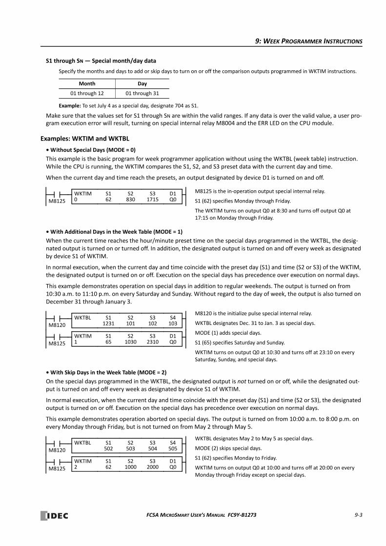
9: WEEK PROGRAMMER INSTRUCTIONS
S1 through SN — Special month/day data
Specify the months and days to add or skip days to turn on or off the comparison outputs programmed in WKTIM instructions.
Example: To set July 4 as a special day, designate 704 as S1.
Make sure that the values set for S1 through SN are within the valid ranges. If any data is over the valid value, a user pro‐gram execution error will result, turning on special internal relay M8004 and the ERR LED on the CPU module.
Examples: WKTIM and WKTBL
• Without Special Days (MODE = 0)
This example is the basic program for week programmer application without using the WKTBL (week table) instruction. While the CPU is running, the WKTIM compares the S1, S2, and S3 preset data with the current day and time.
When the current day and time reach the presets, an output designated by device D1 is turned on and off.
• With Additional Days in the Week Table (MODE = 1)
When the current time reaches the hour/minute preset time on the special days programmed in the WKTBL, the desig‐nated output is turned on or turned off. In addition, the designated output is turned on and off every week as designated by device S1 of WKTIM.
In normal execution, when the current day and time coincide with the preset day (S1) and time (S2 or S3) of the WKTIM, the designated output is turned on or off. Execution on the special days has precedence over execution on normal days.
This example demonstrates operation on special days in addition to regular weekends. The output is turned on from 10:30 a.m. to 11:10 p.m. on every Saturday and Sunday. Without regard to the day of week, the output is also turned on December 31 through January 3.
• With Skip Days in the Week Table (MODE = 2)
On the special days programmed in the WKTBL, the designated output is not turned on or off, while the designated out‐put is turned on and off every week as designated by device S1 of WKTIM.
In normal execution, when the current day and time coincide with the preset day (S1) and time (S2 or S3), the designated output is turned on or off. Execution on the special days has precedence over execution on normal days.
This example demonstrates operation aborted on special days. The output is turned on from 10:00 a.m. to 8:00 p.m. on every Monday through Friday, but is not turned on from May 2 through May 5.
Month Day
01 through 12 01 through 31
D1Q0
S162M8125
WKTIM0
S2830
S31715
M8125 is the in‐operation output special internal relay.
S1 (62) specifies Monday through Friday.
The WKTIM turns on output Q0 at 8:30 and turns off output Q0 at 17:15 on Monday through Friday.
D1Q0
S165
WKTIM1
S21030
S32310
M8120 is the initialize pulse special internal relay.
WKTBL designates Dec. 31 to Jan. 3 as special days.
MODE (1) adds special days.
S1 (65) specifies Saturday and Sunday.
WKTIM turns on output Q0 at 10:30 and turns off at 23:10 on every Saturday, Sunday, and special days.
S4103
S11231M8120
S2101
S3102
WKTBL
M8125
D1Q0
S162
S21000
S32000
WKTBL designates May 2 to May 5 as special days.
MODE (2) skips special days.
S1 (62) specifies Monday to Friday.
WKTIM turns on output Q0 at 10:00 and turns off at 20:00 on every Monday through Friday except on special days.
S4505
S1502M8120
S2503
S3504
M8125
WKTBL
WKTIM2
FC5A MICROSMART USER’S MANUAL FC9Y‐B1273 9‐3
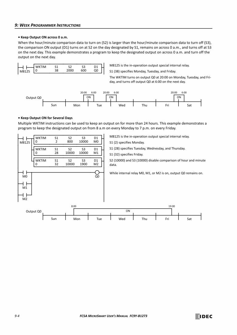
9: WEEK PROGRAMMER INSTRUCTIONS
• Keep Output ON across 0 a.m.
When the hour/minute comparison data to turn on (S2) is larger than the hour/minute comparison data to turn off (S3), the comparison ON output (D1) turns on at S2 on the day designated by S1, remains on across 0 a.m., and turns off at S3 on the next day. This example demonstrates a program to keep the designated output on across 0 a.m. and turn off the output on the next day.
• Keep Output ON for Several Days
Multiple WKTIM instructions can be used to keep an output on for more than 24 hours. This example demonstrates a program to keep the designated output on from 8 a.m on every Monday to 7 p.m. on every Friday.
D1Q0
S138M8125
WKTIM0
S22000
S3600
M8125 is the in‐operation output special internal relay.
S1 (38) specifies Monday, Tuesday, and Friday.
The WKTIM turns on output Q0 at 20:00 on Monday, Tuesday, and Fri‐day, and turns off output Q0 at 6:00 on the next day.
Sun Mon Tue Wed Thu Fri Sat
20:00 6:00
ONOutput Q0
20:00 6:00
ON
20:00 6:00
ON
D1M0
S12M8125
WKTIM0
S2800
S310000
M8125 is the in‐operation output special internal relay.
S1 (2) specifies Monday.
S1 (28) specifies Tuesday, Wednesday, and Thursday.
S1 (32) specifies Friday.
S2 (10000) and S3 (10000) disable comparison of hour and minute data.
While internal relay M0, M1, or M2 is on, output Q0 remains on.
Sun Mon Tue Wed Thu Fri Sat
8:00 19:00
ONOutput Q0
D1M1
S128
WKTIM0
S210000
S310000
D1M2
S132
WKTIM0
S210000
S31900
M0
M1
M2
Q0
9‐4 FC5A MICROSMART USER’S MANUAL FC9Y‐B1273
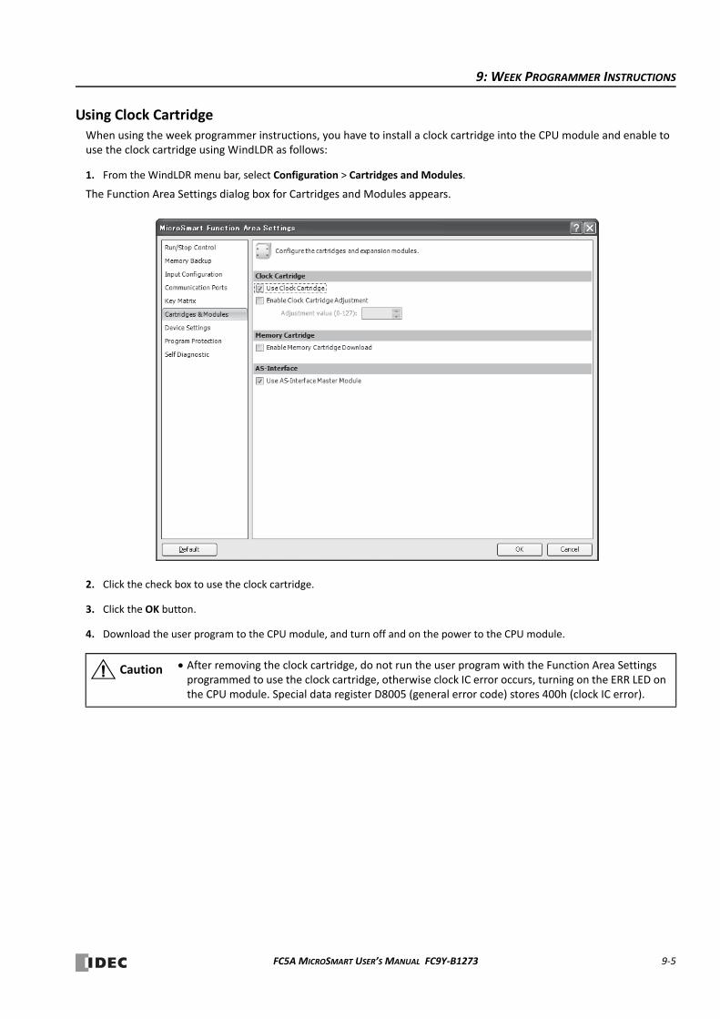
9: WEEK PROGRAMMER INSTRUCTIONS
Using Clock CartridgeWhen using the week programmer instructions, you have to install a clock cartridge into the CPU module and enable to use the clock cartridge using WindLDR as follows:
1. From the WindLDR menu bar, select Configuration > Cartridges and Modules.
The Function Area Settings dialog box for Cartridges and Modules appears.
2. Click the check box to use the clock cartridge.
3. Click the OK button.
4. Download the user program to the CPU module, and turn off and on the power to the CPU module.
After removing the clock cartridge, do not run the user program with the Function Area Settings programmed to use the clock cartridge, otherwise clock IC error occurs, turning on the ERR LED on the CPU module. Special data register D8005 (general error code) stores 400h (clock IC error).
Caution
FC5A MICROSMART USER’S MANUAL FC9Y‐B1273 9‐5

9: WEEK PROGRAMMER INSTRUCTIONS
Setting Calendar/Clock Using WindLDRBefore using the clock cartridge for the first time, the calendar/clock data in the clock cartridge must be set using WindLDR or executing a user program to transfer correct calendar/clock data from special data registers allocated to the calendar/clock. Once the calendar/clock data is stored, the data is held by the backup battery in the clock cartridge.
1. Select Online from the WindLDR menu bar, then select Monitor. The screen display changes to the monitor window.
2. From the PLC menu, select Status. The MicroSmart PLC Status dialog box is displayed. The current calendar/clock data is read out from the clock cartridge and displayed in the Calendar field.
3. Click the Change button for the Calendar. The Set Calendar and Time dialog box comes up with the date and time values read from the computer internal clock.
4. Click the Down Arrow button on the right of Calendar, then a calendar is displayed where you can change the year, month, and date. Enter or select new values.
5. To change hours and minutes, click in the Time box, and type a new value or use the up/down keys. When new values are entered, click the OK button to transfer the new values to the clock cartridge.
Setting Calendar/Clock Using a User ProgramAnother way of setting the calendar/clock data is to store the values in special data registers dedicated to the calendar and clock and to turn on special internal relay M8016, M8017, or M8020. Data registers D8015 through D8021 do not hold the current values of the calendar/clock data but hold unknown values before executing a user program.
Special Data Registers for Calendar/Clock Data
Note: The day of week value is assigned for both current and new data as follows:
Data Register No. Data Value Read/Write Updated
D8008 Year (current data) 0 to 99
Read only500 ms or one scan time whichever is larger
D8009 Month (current data) 1 to 12
D8010 Day (current data) 1 to 31
D8011 Day of week (current data) 0 to 6 (Note)
D8012 Hour (current data) 0 to 23
D8013 Minute (current data) 0 to 59
D8014 Second (current data) 0 to 59
D8015 Year (new data) 0 to 99
Write only Not updated
D8016 Month (new data) 1 to 12
D8017 Day (new data) 1 to 31
D8018 Day of week (new data) 0 to 6 (Note)
D8019 Hour (new data) 0 to 23
D8020 Minute (new data) 0 to 59
D8021 Second (new data) 0 to 59
0 1 2 3 4 5 6
Sunday Monday Tuesday Wednesday Thursday Friday Saturday
9‐6 FC5A MICROSMART USER’S MANUAL FC9Y‐B1273
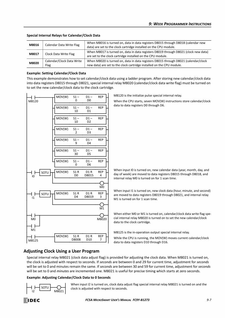
9: WEEK PROGRAMMER INSTRUCTIONS
Special Internal Relays for Calendar/Clock Data
Example: Setting Calendar/Clock Data
This example demonstrates how to set calendar/clock data using a ladder program. After storing new calendar/clock data into data registers D8015 through D8021, special internal relay M8020 (calendar/clock data write flag) must be turned on to set the new calendar/clock data to the clock cartridge.
Adjusting Clock Using a User ProgramSpecial internal relay M8021 (clock data adjust flag) is provided for adjusting the clock data. When M8021 is turned on, the clock is adjusted with respect to seconds. If seconds are between 0 and 29 for current time, adjustment for seconds will be set to 0 and minutes remain the same. If seconds are between 30 and 59 for current time, adjustment for seconds will be set to 0 and minutes are incremented one. M8021 is useful for precise timing which starts at zero seconds.
Example: Adjusting Calendar/Clock Data to 0 Seconds
M8016 Calendar Data Write FlagWhen M8016 is turned on, data in data registers D8015 through D8018 (calendar new data) are set to the clock cartridge installed on the CPU module.
M8017 Clock Data Write FlagWhen M8017 is turned on, data in data registers D8019 through D8021 (clock new data) are set to the clock cartridge installed on the CPU module.
M8020Calendar/Clock Data Write Flag
When M8020 is turned on, data in data registers D8015 through D8021 (calendar/clock new data) are set to the clock cartridge installed on the CPU module.
M8120
REP4
S1 RD0
MOV(W) D1 RD8015I0
SOTU
M8120 is the initialize pulse special internal relay.
When the CPU starts, seven MOV(W) instructions store calendar/clock data to data registers D0 through D6.
When input I0 is turned on, new calendar data (year, month, day, and day of week) are moved to data registers D8015 through D8018, and internal relay M0 is turned on for 1 scan time.
When input I1 is turned on, new clock data (hour, minute, and second) are moved to data registers D8019 through D8021, and internal relay M1 is turned on for 1 scan time.
When either M0 or M1 is turned on, calendar/clock data write flag spe‐cial internal relay M8020 is turned on to set the new calendar/clock data to the clock cartridge.
M8125 is the in‐operation output special internal relay.
While the CPU is running, the MOV(W) moves current calendar/clock data to data registers D10 through D16.
REP3
S1 RD4
MOV(W) D1 RD8019I1
SOTU
M0
M1
REP7
S1 RD8008
MOV(W) D1 RD10M8125
M1
M8020
REPS1 –0
MOV(W) D1 –D0
REPS1 –10
MOV(W) D1 –D1
REPS1 –10
MOV(W) D1 –D2
REPS1 –2
MOV(W) D1 –D3
REPS1 –9
MOV(W) D1 –D4
REPS1 –30
MOV(W) D1 –D5
REPS1 –0
MOV(W) D1 –D6
M0
I2SOTU
When input I2 is turned on, clock data adjust flag special internal relay M8021 is turned on and the clock is adjusted with respect to seconds.
M8021
FC5A MICROSMART USER’S MANUAL FC9Y‐B1273 9‐7
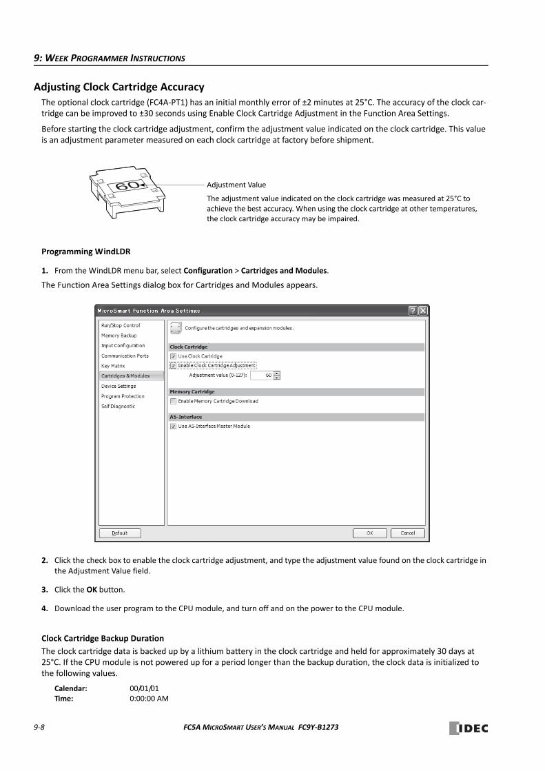
9: WEEK PROGRAMMER INSTRUCTIONS
Adjusting Clock Cartridge AccuracyThe optional clock cartridge (FC4A‐PT1) has an initial monthly error of ±2 minutes at 25°C. The accuracy of the clock car‐tridge can be improved to ±30 seconds using Enable Clock Cartridge Adjustment in the Function Area Settings.
Before starting the clock cartridge adjustment, confirm the adjustment value indicated on the clock cartridge. This value is an adjustment parameter measured on each clock cartridge at factory before shipment.
Programming WindLDR
1. From the WindLDR menu bar, select Configuration > Cartridges and Modules.
The Function Area Settings dialog box for Cartridges and Modules appears.
2. Click the check box to enable the clock cartridge adjustment, and type the adjustment value found on the clock cartridge in the Adjustment Value field.
3. Click the OK button.
4. Download the user program to the CPU module, and turn off and on the power to the CPU module.
Clock Cartridge Backup Duration
The clock cartridge data is backed up by a lithium battery in the clock cartridge and held for approximately 30 days at 25°C. If the CPU module is not powered up for a period longer than the backup duration, the clock data is initialized to the following values.
Calendar: 00/01/01Time: 0:00:00 AM
Adjustment Value
The adjustment value indicated on the clock cartridge was measured at 25°C to achieve the best accuracy. When using the clock cartridge at other temperatures, the clock cartridge accuracy may be impaired.
9‐8 FC5A MICROSMART USER’S MANUAL FC9Y‐B1273

10: INTERFACE INSTRUCTIONS
IntroductionThe DISP (display) instruction is used to display 1 through 5 digits of timer/counter current values and data register data on 7‐segment display units.
The DGRD (digital read) instruction is used to read 1 through 5 digits of digital switch settings to a data register. This instruction is useful to change preset values for timers and counters using digital switches.
DISP (Display)
Applicable CPU Modules
Note: The DISP instruction requires transistor output terminals. When using all‐in‐one 24‐I/O type CPU module FC5A‐C24R2, connect a transistor output module.
Valid Devices
For the valid device address range, see pages 6‐1 and 6‐2 (Basic Vol.).
Internal relays M0 through M2557 can be designated as Q. Special internal relays cannot be designated as Q.When T (timer) or C (counter) is used as S1, the timer/counter current value (TC or CC) is read out.
Conversion
BCD: To connect BCD (decimal) display unitsBIN: To connect BIN (hexadecimal) display units
Latch Phase and Data Phase
Select the latch and data phases to match the phases of the display units in consideration of sink or source output of the output module.
Output Points
The quantity of required output points is 4 plus the quantity of digits to display. When displaying 4 digits with output Q0 designated as the first output number, 8 consecutive output points must be reserved starting with Q0 through Q7.
Display Processing Time
Displaying one digit of data requires 3 scan times after the input to the DISP instruction is turned on. Keep the input to the DISP instruction for the period of time shown below to process all digits of the display data.
When the scan time is less than 2 ms, the data cannot be displayed correctly. When the scan time is too short to ensure normal display, set a value of 3 or more (in ms) to data register D8022 (constant scan time preset value). See page 5‐50 (Basic Vol.).
FC5A‐C10R2/C/D FC5A‐C16R2/C/D FC5A‐C24R2/C/D FC5A‐D16RK1/RS1 FC5A‐D32K3/S3 FC5A‐D12K1E/S1E
— — X X X X
Device Function I Q M R T C D Constant Repeat
S1 (Source 1) Data to display — — — — X X X — —
Q (Output) First output number to display data — X — — — — — —
Display Processing Time3 scan times Quantity of digits
Latch phase:Low or High
Data phase:Low or High
Conversion:BCD or BIN
When input is on, data designated by source device S1 is set to outputs or internal relays designated by device Q. This instruc‐tion is used to output 7‐segment data to display units.
Eight DISP instructions can be used in a user program.
Display data can be 0 through 65535 (FFFFh).
DISP DATS1*****
Q*****BCD4
LATLL
Quantity of digits:1 to 5 (decimal)1 to 4 (hex)
FC5A MICROSMART USER’S MANUAL FC9Y‐B1273 10‐1

10: INTERFACE INSTRUCTIONS
Example: DISP
The following example demonstrates a program to display the 4‐digit current value of counter CNT10 on 7‐segment dis‐play units (IDEC’s DD3S‐F31N) connected to the transistor sink output module.
Output Wiring Diagram
When input I0 is on, the 4‐digit current value of counter C10 is displayed on 7‐segment digital display units.I0
DATLATHL
S1C10
QQ30
DISPBCD4
(+)(–)
LatchABCD
(+)
(–)
24V DCPowerSupply
(+)(–)
LatchABCD
(+)(–)
LatchABCD
(+)(–)
LatchABCD
103 102 101 100
8‐Transistor Sink
Upper Digit Lower Digit
FC4A‐T08K1Output Module
Q30Q31Q32Q33Q34Q35Q36Q37
COM(–)+V
10‐2 FC5A MICROSMART USER’S MANUAL FC9Y‐B1273

10: INTERFACE INSTRUCTIONS
DGRD (Digital Read)
Applicable CPU Modules
Note: The DGRD instruction requires transistor output terminals. When using all‐in‐one 24‐I/O type CPU module FC5A‐C24R2, connect a transistor output module.
Valid Devices
For the valid device address range, see pages 6‐1 and 6‐2 (Basic Vol.).
The DGRD instruction can read 65535 (5 digits) at the maximum. When the read value exceeds 65535 with the quantity of digits set to 5, a user program execution error will result, turning on special internal relay M8004 and the ERR LED on the CPU module.
Note: The DGRD instruction can be used up to 16 times in a user program. When transferring a user program containing more than 16 DGRD instructions to the CPU, a user program syntax error occurs, turning on the ERR LED. The user program cannot be executed.
Conversion
BCD: To connect BCD (decimal) digital switchesBIN: To connect BIN (hexadecimal) digital switches
Input Points
Inputs are used to read the data from digital switches. The quantity of required input points is always 4. Four input points must be reserved starting with the input number designated by device I. For example, when input I0 is designated as device I, inputs I0 through I3 are used.
When using input terminals on the CPU module, the filter value has an effect (default value is 3 ms). Input terminals on expansion input modules have a fixed filter value of 4 ms. For Input Filter, see page 5‐42 (Basic Vol.).
Output Points
Outputs are used to select the digits to read. The quantity of required output points is equal to the quantity of digits to read. When connecting the maximum of 5 digital switches, 5 output points must be reserved starting with the output number designated by device Q. For example, when output Q0 is designated as device Q to read 3 digits, outputs Q0 through Q2 are used.
Digital Switch Data Reading Time
Reading digital switch data requires the following time after the input to the DGRD instruction is turned on. Keep the input to the DGRD instruction for the period of time shown below to read the digital switch data. For example, when reading data from 5 digital switches to the destination device, 14 scans are required.
FC5A‐C10R2/C/D FC5A‐C16R2/C/D FC5A‐C24R2/C/D FC5A‐D16RK1/RS1 FC5A‐D32K3/S3 FC5A‐D12K1E/S1E
— — X X X X
Device Function I Q M R T C D Constant Repeat
I First input number to read X — — — — — — — —
Q First output number for digit selection — X — — — — — — —
D1 (Destination 1) Destination to store results — — — — — — X — —
Digital Switch Data Reading Time2 scan times (Quantity of digits + 2)
First input number
First output number
Conversion:BCD or BIN
Quantity of digits:1 to 5 (decimal)1 to 4 (hex)
When input is on, data designated by devices I and Q is set to a data register designated by destination device D1.
This instruction can be used to change preset values for timer and counter instructions using digital switches. The data that can be read using this instruction is 0 through 65535 (5 digits), or FFFFh.
DGRD I*****
Q*****BCD4
D1*****
FC5A MICROSMART USER’S MANUAL FC9Y‐B1273 10‐3
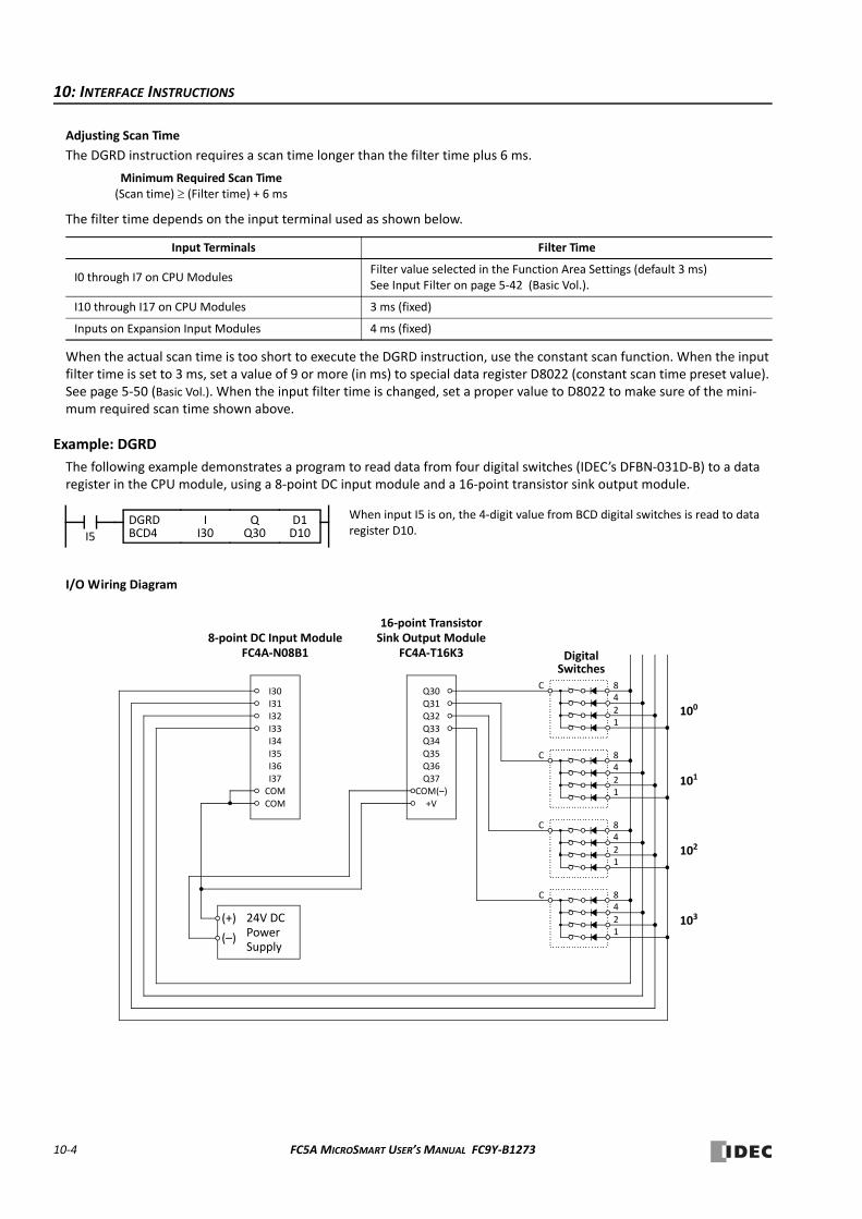
10: INTERFACE INSTRUCTIONS
Adjusting Scan Time
The DGRD instruction requires a scan time longer than the filter time plus 6 ms.
The filter time depends on the input terminal used as shown below.
When the actual scan time is too short to execute the DGRD instruction, use the constant scan function. When the input filter time is set to 3 ms, set a value of 9 or more (in ms) to special data register D8022 (constant scan time preset value). See page 5‐50 (Basic Vol.). When the input filter time is changed, set a proper value to D8022 to make sure of the mini‐mum required scan time shown above.
Example: DGRD
The following example demonstrates a program to read data from four digital switches (IDEC’s DFBN‐031D‐B) to a data register in the CPU module, using a 8‐point DC input module and a 16‐point transistor sink output module.
I/O Wiring Diagram
Minimum Required Scan Time(Scan time) (Filter time) + 6 ms
Input Terminals Filter Time
I0 through I7 on CPU ModulesFilter value selected in the Function Area Settings (default 3 ms)See Input Filter on page 5‐42 (Basic Vol.).
I10 through I17 on CPU Modules 3 ms (fixed)
Inputs on Expansion Input Modules 4 ms (fixed)
When input I5 is on, the 4‐digit value from BCD digital switches is read to data register D10.I5
II30
QQ30
D1D10
DGRDBCD4
Digital
12
48
Switches
8‐point DC Input ModuleFC4A‐N08B1
16‐point Transistor
FC4A‐T16K3
103
102
101
100Q30Q31Q32Q33Q34Q35Q36Q37
COM(–)+V
(+)
(–)
24V DCPowerSupply
I30I31I32I33I34I35I36I37COMCOM
C
12
48C
1248C
12
48C
Sink Output Module
10‐4 FC5A MICROSMART USER’S MANUAL FC9Y‐B1273
11: PROGRAM BRANCHING INSTRUCTIONS
IntroductionThe program branching instructions reduce execution time by making it possible to bypass portions of the program whenever certain conditions are not satisfied.
The basic program branching instructions are LABEL and LJMP, which are used to tag an address and jump to the address which has been tagged. Programming tools include “either/or” options between numerous portions of a program and the ability to call one of several subroutines which return execution to where the normal program left off.
The DI or EI instruction disables or enables interrupt inputs and timer interrupt individually.
LABEL (Label)
Applicable CPU Modules
Valid Devices
LJMP (Label Jump)
Applicable CPU Modules
Valid Devices
For the valid device address range, see pages 6‐1 and 6‐2 (Basic Vol.).
Since the LJMP instruction is executed in each scan while input is on, a pulse input from a SOTU or SOTD instruction should be used as required.
Note: Make sure that a LABEL instruction of the label number used for a LJMP instruction is programmed. When designating S1 using other than a constant, the value for the label is a variable. When using a variable for a label, make sure that all probable LABEL num‐bers are included in the user program. If a matching label does not exist, a user program execution error will result, turning on special internal relay M8004 and the ERR LED on the CPU module.
FC5A‐C10R2/C/D FC5A‐C16R2/C/D FC5A‐C24R2/C/D FC5A‐D16RK1/RS1 FC5A‐D32K3/S3 FC5A‐D12K1E/S1E
X X X X X X
Device Function I Q M R T C D Constant Repeat
Label number Tag for LJMP and LCAL — — — — — — — 0‐127, 0‐255 —
FC5A‐C10R2/C/D FC5A‐C16R2/C/D FC5A‐C24R2/C/D FC5A‐D16RK1/RS1 FC5A‐D32K3/S3 FC5A‐D12K1E/S1E
X X X X X X
Device Function I Q M R T C D Constant Repeat
S1 (Source 1) Label number to jump to — — — — — — X 0‐127, 0‐255 —
This is the label number, from 0 to 127 (all‐in‐one type CPU) or 0 to 255 (slim type CPU), used at the pro‐gram address where the execution of program instructions begins for a program branch.
An END instruction may be used to separate a tagged portion of the program from the main program. In this way, scan time is minimized by not executing the program branch unless input conditions are satisfied.
Note: The same label number cannot be used more than once.
LABEL***
When input is on, jump to the address with label 0 through 127 (all‐in‐one type CPU) or 0 to 255 (slim type CPU) designated by S1.
When input is off, no jump takes place, and program execution proceeds with the next instruc‐tion.
The LJMP instruction is used as an “either/or” choice between two portions of a program. Pro‐gram execution does not return to the instruction following the LJMP instruction, after the pro‐gram branch.
LJMP S1*****
FC5A MICROSMART USER’S MANUAL FC9Y‐B1273 11‐1
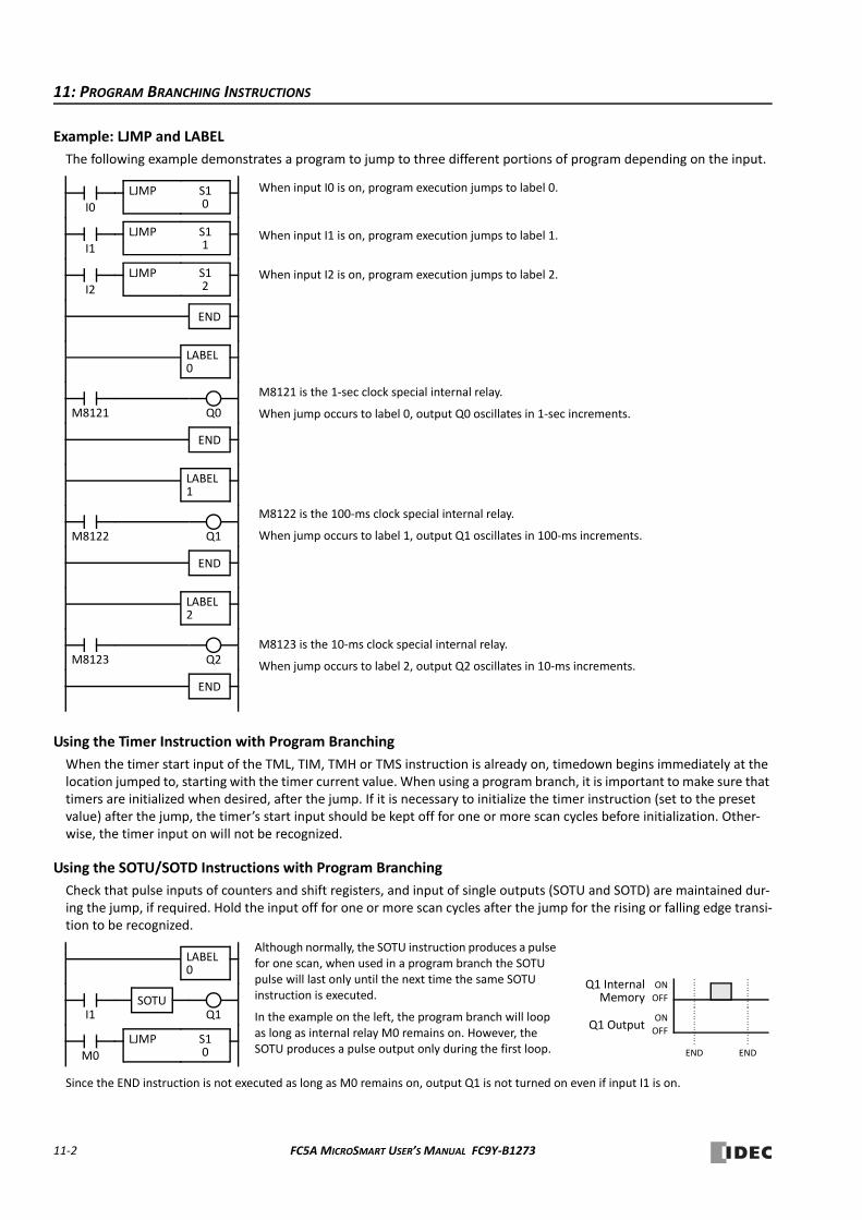
11: PROGRAM BRANCHING INSTRUCTIONS
Example: LJMP and LABEL
The following example demonstrates a program to jump to three different portions of program depending on the input.
Using the Timer Instruction with Program Branching
When the timer start input of the TML, TIM, TMH or TMS instruction is already on, timedown begins immediately at the location jumped to, starting with the timer current value. When using a program branch, it is important to make sure that timers are initialized when desired, after the jump. If it is necessary to initialize the timer instruction (set to the preset value) after the jump, the timer’s start input should be kept off for one or more scan cycles before initialization. Other‐wise, the timer input on will not be recognized.
Using the SOTU/SOTD Instructions with Program Branching
Check that pulse inputs of counters and shift registers, and input of single outputs (SOTU and SOTD) are maintained dur‐ing the jump, if required. Hold the input off for one or more scan cycles after the jump for the rising or falling edge transi‐tion to be recognized.
When input I0 is on, program execution jumps to label 0.
When input I1 is on, program execution jumps to label 1.
When input I2 is on, program execution jumps to label 2.
M8121 is the 1‐sec clock special internal relay.
When jump occurs to label 0, output Q0 oscillates in 1‐sec increments.
M8122 is the 100‐ms clock special internal relay.
When jump occurs to label 1, output Q1 oscillates in 100‐ms increments.
M8123 is the 10‐ms clock special internal relay.
When jump occurs to label 2, output Q2 oscillates in 10‐ms increments.
LABEL0
I0
LJMP S10
END
I1
LJMP S11
I2
LJMP S12
M8121
END
M8122
END
M8123
END
Q0
Q1
Q2
LABEL1
LABEL2
I1SOTU
M0
LJMP S10
Although normally, the SOTU instruction produces a pulse for one scan, when used in a program branch the SOTU pulse will last only until the next time the same SOTU instruction is executed.
In the example on the left, the program branch will loop as long as internal relay M0 remains on. However, the SOTU produces a pulse output only during the first loop.
Q1 Internal ON
OFF
Q1 OutputON
OFF
Memory
END END
Q1
LABEL0
Since the END instruction is not executed as long as M0 remains on, output Q1 is not turned on even if input I1 is on.
11‐2 FC5A MICROSMART USER’S MANUAL FC9Y‐B1273
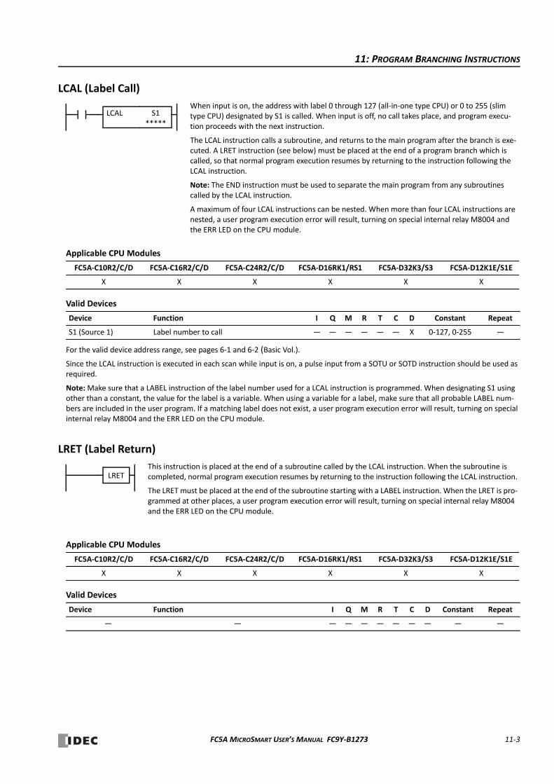
11: PROGRAM BRANCHING INSTRUCTIONS
LCAL (Label Call)
Applicable CPU Modules
Valid Devices
For the valid device address range, see pages 6‐1 and 6‐2 (Basic Vol.).
Since the LCAL instruction is executed in each scan while input is on, a pulse input from a SOTU or SOTD instruction should be used as required.
Note: Make sure that a LABEL instruction of the label number used for a LCAL instruction is programmed. When designating S1 using other than a constant, the value for the label is a variable. When using a variable for a label, make sure that all probable LABEL num‐bers are included in the user program. If a matching label does not exist, a user program execution error will result, turning on special internal relay M8004 and the ERR LED on the CPU module.
LRET (Label Return)
Applicable CPU Modules
Valid Devices
FC5A‐C10R2/C/D FC5A‐C16R2/C/D FC5A‐C24R2/C/D FC5A‐D16RK1/RS1 FC5A‐D32K3/S3 FC5A‐D12K1E/S1E
X X X X X X
Device Function I Q M R T C D Constant Repeat
S1 (Source 1) Label number to call — — — — — — X 0‐127, 0‐255 —
FC5A‐C10R2/C/D FC5A‐C16R2/C/D FC5A‐C24R2/C/D FC5A‐D16RK1/RS1 FC5A‐D32K3/S3 FC5A‐D12K1E/S1E
X X X X X X
Device Function I Q M R T C D Constant Repeat
— — — — — — — — — — —
When input is on, the address with label 0 through 127 (all‐in‐one type CPU) or 0 to 255 (slim type CPU) designated by S1 is called. When input is off, no call takes place, and program execu‐tion proceeds with the next instruction.
The LCAL instruction calls a subroutine, and returns to the main program after the branch is exe‐cuted. A LRET instruction (see below) must be placed at the end of a program branch which is called, so that normal program execution resumes by returning to the instruction following the LCAL instruction.
Note: The END instruction must be used to separate the main program from any subroutines called by the LCAL instruction.
A maximum of four LCAL instructions can be nested. When more than four LCAL instructions are nested, a user program execution error will result, turning on special internal relay M8004 and the ERR LED on the CPU module.
LCAL S1*****
This instruction is placed at the end of a subroutine called by the LCAL instruction. When the subroutine is completed, normal program execution resumes by returning to the instruction following the LCAL instruction.
The LRET must be placed at the end of the subroutine starting with a LABEL instruction. When the LRET is pro‐grammed at other places, a user program execution error will result, turning on special internal relay M8004 and the ERR LED on the CPU module.
LRET
FC5A MICROSMART USER’S MANUAL FC9Y‐B1273 11‐3

11: PROGRAM BRANCHING INSTRUCTIONS
Correct Structure for Calling Subroutine
When a LCAL instruction is executed, the remaining program instructions on the same rung may not be executed upon return, if input conditions are changed by the subroutine. After the LRET instruction of a subroutine, program execution begins with the instruction following the LCAL instruction, depending on current input condition.
When instructions following a LCAL instruction must be executed after the subroutine is called, make sure the subroutine does not change input conditions unfavorably. In addition, include subsequent instructions in a new ladder line, sepa‐rated from the LCAL instruction.
Example: LCAL and LRET
The following example demonstrates a program to call three different portions of program depending on the input. When the subroutine is complete, program execution returns to the instruction following the LCAL instruction.
I0
LCAL S10
REPS1 –D0
D1 –D1
MOV(W)
REPS1 –D20
D1 –D21
MOV(W)
Correct
I0
LCAL S10
REPS1 –D0
D1 –D1
MOV(W)
REPS1 –D20
D1 –D21
MOV(W)
Incorrect
Separate the ladder line for each LCAL instruction. I0 status may be changed by the subroutine upon return.
M0S
M0S
I0
When input I0 is on, program execution jumps to label 0.
When input I1 is on, program execution jumps to label 1.
When input I2 is on, program execution jumps to label 2.
M8121 is the 1‐sec clock special internal relay.
When jump occurs to label 0, output Q0 oscillates in 1‐sec increments.
Program execution returns to the address of input I1.
M8122 is the 100‐ms clock special internal relay.
When jump occurs to label 1, output Q1 oscillates in 100‐ms increments.
Program execution returns to the address of input I2.
M8123 is the 10‐ms clock special internal relay.
When jump occurs to label 2, output Q2 oscillates in 10‐ms increments.
Program execution returns to the address of END.
I0
LCAL S10
END
I1
LCAL S11
I2
LCAL S12
M8121
LRET
M8122
LRET
M8123
LRET
Q0
Q1
Q2
LABEL0
LABEL1
LABEL2
11‐4 FC5A MICROSMART USER’S MANUAL FC9Y‐B1273
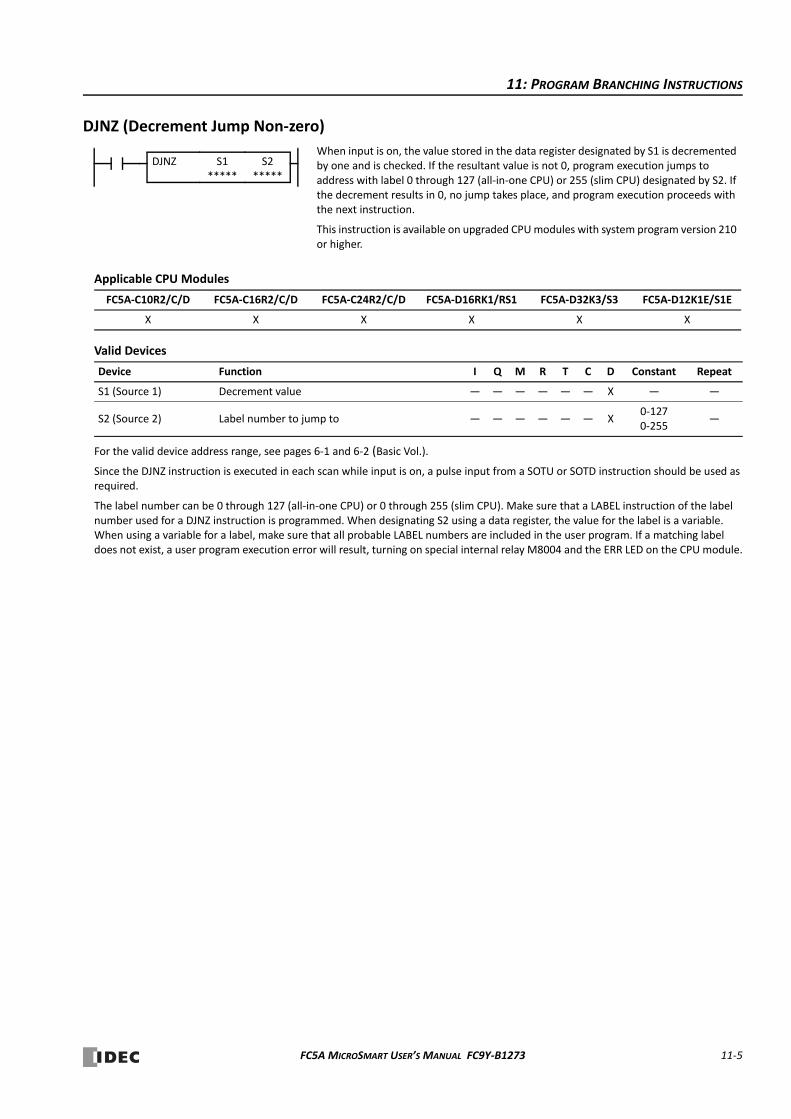
11: PROGRAM BRANCHING INSTRUCTIONS
DJNZ (Decrement Jump Non‐zero)
Applicable CPU Modules
Valid Devices
For the valid device address range, see pages 6‐1 and 6‐2 (Basic Vol.).
Since the DJNZ instruction is executed in each scan while input is on, a pulse input from a SOTU or SOTD instruction should be used as required.
The label number can be 0 through 127 (all‐in‐one CPU) or 0 through 255 (slim CPU). Make sure that a LABEL instruction of the label number used for a DJNZ instruction is programmed. When designating S2 using a data register, the value for the label is a variable. When using a variable for a label, make sure that all probable LABEL numbers are included in the user program. If a matching label does not exist, a user program execution error will result, turning on special internal relay M8004 and the ERR LED on the CPU module.
FC5A‐C10R2/C/D FC5A‐C16R2/C/D FC5A‐C24R2/C/D FC5A‐D16RK1/RS1 FC5A‐D32K3/S3 FC5A‐D12K1E/S1E
X X X X X X
Device Function I Q M R T C D Constant Repeat
S1 (Source 1) Decrement value — — — — — — X — —
S2 (Source 2) Label number to jump to — — — — — — X0‐1270‐255
—
When input is on, the value stored in the data register designated by S1 is decremented by one and is checked. If the resultant value is not 0, program execution jumps to address with label 0 through 127 (all‐in‐one CPU) or 255 (slim CPU) designated by S2. If the decrement results in 0, no jump takes place, and program execution proceeds with the next instruction.
This instruction is available on upgraded CPU modules with system program version 210 or higher.
DJNZ S1*****
S2*****
FC5A MICROSMART USER’S MANUAL FC9Y‐B1273 11‐5
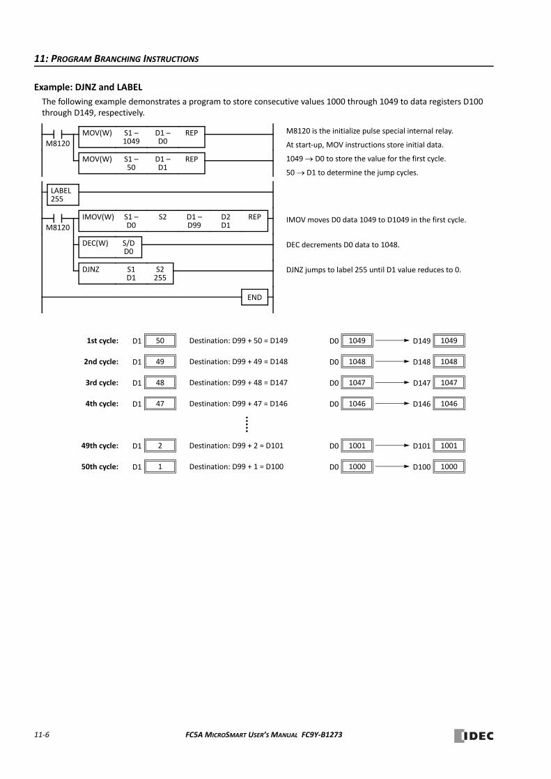
11: PROGRAM BRANCHING INSTRUCTIONS
Example: DJNZ and LABEL
The following example demonstrates a program to store consecutive values 1000 through 1049 to data registers D100 through D149, respectively.
M8120 is the initialize pulse special internal relay.
At start‐up, MOV instructions store initial data.
1049 D0 to store the value for the first cycle.
50 D1 to determine the jump cycles.
IMOV moves D0 data 1049 to D1049 in the first cycle.
DEC decrements D0 data to 1048.
DJNZ jumps to label 255 until D1 value reduces to 0.
LABEL255
M8120
END
M8120
REPS1 –D0
D1 –D99
IMOV(W) S2 D2D1
REPS1 –1049
D1 –D0
MOV(W)
REPS1 –50
D1 –D1
MOV(W)
S/DD0
DEC(W)
S2255
S1D1
DJNZ
1049D0Destination: D99 + 50 = D149 1049D14950D11st cycle:
1048D0Destination: D99 + 49 = D148 1048D14849D12nd cycle:
1047D0Destination: D99 + 48 = D147 1047D14748D13rd cycle:
1046D0Destination: D99 + 47 = D146 1046D14647D14th cycle:
1001D0Destination: D99 + 2 = D101 1001D1012D149th cycle:
1000D0Destination: D99 + 1 = D100 1000D1001D150th cycle:
11‐6 FC5A MICROSMART USER’S MANUAL FC9Y‐B1273
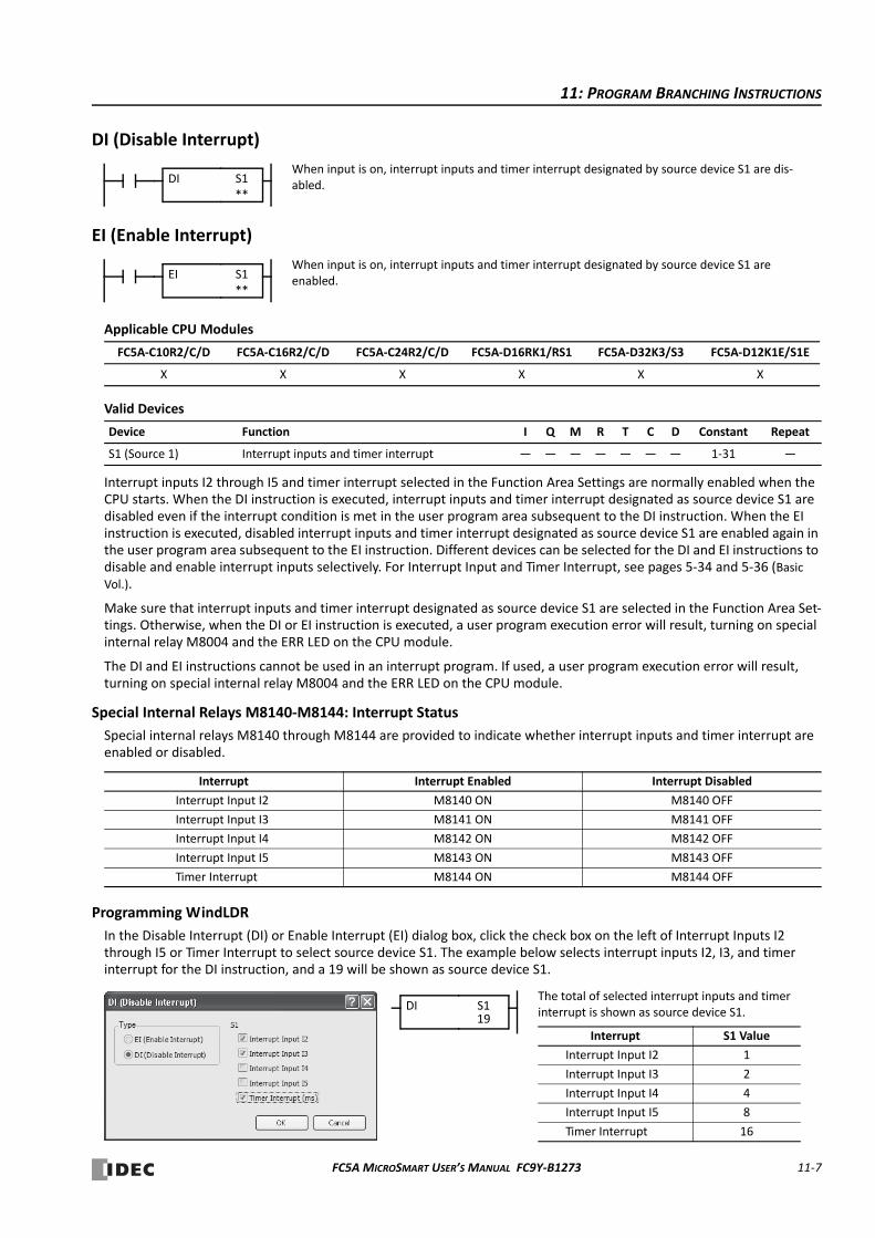
11: PROGRAM BRANCHING INSTRUCTIONS
DI (Disable Interrupt)
EI (Enable Interrupt)
Applicable CPU Modules
Valid Devices
Interrupt inputs I2 through I5 and timer interrupt selected in the Function Area Settings are normally enabled when the CPU starts. When the DI instruction is executed, interrupt inputs and timer interrupt designated as source device S1 are disabled even if the interrupt condition is met in the user program area subsequent to the DI instruction. When the EI instruction is executed, disabled interrupt inputs and timer interrupt designated as source device S1 are enabled again in the user program area subsequent to the EI instruction. Different devices can be selected for the DI and EI instructions to disable and enable interrupt inputs selectively. For Interrupt Input and Timer Interrupt, see pages 5‐34 and 5‐36 (Basic Vol.).
Make sure that interrupt inputs and timer interrupt designated as source device S1 are selected in the Function Area Set‐tings. Otherwise, when the DI or EI instruction is executed, a user program execution error will result, turning on special internal relay M8004 and the ERR LED on the CPU module.
The DI and EI instructions cannot be used in an interrupt program. If used, a user program execution error will result, turning on special internal relay M8004 and the ERR LED on the CPU module.
Special Internal Relays M8140‐M8144: Interrupt Status
Special internal relays M8140 through M8144 are provided to indicate whether interrupt inputs and timer interrupt are enabled or disabled.
Programming WindLDR
In the Disable Interrupt (DI) or Enable Interrupt (EI) dialog box, click the check box on the left of Interrupt Inputs I2 through I5 or Timer Interrupt to select source device S1. The example below selects interrupt inputs I2, I3, and timer interrupt for the DI instruction, and a 19 will be shown as source device S1.
FC5A‐C10R2/C/D FC5A‐C16R2/C/D FC5A‐C24R2/C/D FC5A‐D16RK1/RS1 FC5A‐D32K3/S3 FC5A‐D12K1E/S1E
X X X X X X
Device Function I Q M R T C D Constant Repeat
S1 (Source 1) Interrupt inputs and timer interrupt — — — — — — — 1‐31 —
Interrupt Interrupt Enabled Interrupt Disabled
Interrupt Input I2 M8140 ON M8140 OFF
Interrupt Input I3 M8141 ON M8141 OFF
Interrupt Input I4 M8142 ON M8142 OFF
Interrupt Input I5 M8143 ON M8143 OFF
Timer Interrupt M8144 ON M8144 OFF
When input is on, interrupt inputs and timer interrupt designated by source device S1 are dis‐abled.DI S1
**
EI S1**
When input is on, interrupt inputs and timer interrupt designated by source device S1 are enabled.
DI S119
The total of selected interrupt inputs and timer interrupt is shown as source device S1.
Interrupt S1 Value
Interrupt Input I2 1
Interrupt Input I3 2
Interrupt Input I4 4
Interrupt Input I5 8
Timer Interrupt 16
FC5A MICROSMART USER’S MANUAL FC9Y‐B1273 11‐7

11: PROGRAM BRANCHING INSTRUCTIONS
Example: DI and EI
The following example demonstrates a program to disable and enable interrupt inputs and timer interrupt selectively. For the interrupt input and timer interrupt functions, see pages 5‐34 and 5‐36 (Basic Vol.). In this example, inputs I2 and I3 are designated as interrupt inputs and timer interrupt is used with interrupt intervals of 100 ms.
M8120 is the initialize pulse special internal relay.
D8032 stores jump destination label number 0 for interrupt input I2.
D8033 stores jump destination label number 1 for interrupt input I3.
D8036 stores jump destination label number 2 for timer interrupt.
When input I10 is on, DI disables interrupt inputs I2, I3, and timer interrupt, then M8140, M8141, and M8144 turn off.
When input I11 is on and I10 is off, EI enables interrupt inputs I2 and I3, then M8140 and M8141 turn on.
When input I12 is on and I10 is off, EI enables timer interrupt, then M8144 turns on.
End of the main program.
When input I2 is on, program execution jumps to label 0.
M8125 is the in‐operation output special internal relay.
ALT turns on or off the output Q2 internal memory.
IOREF immediately writes the output Q2 internal memory status to actual out‐put Q2.
Program execution returns to the main program.
When input I3 is on, program execution jumps to label 1.
M8125 is the in‐operation output special internal relay.
ALT turns on or off the output Q3 internal memory.
IOREF immediately writes the output Q3 internal memory status to actual out‐put Q3.
Program execution returns to the main program.
Timer interrupt occurs every 100 ms, then program execution jumps to label 2.
M8125 is the in‐operation output special internal relay.
ALT turns on or off the output Q4 internal memory.
IOREF immediately writes the output Q4 internal memory status to actual out‐put Q4.
Program execution returns to the main program.
M8120
END
I10
REPS1 –0
D1 –D8032
MOV(W)
DI S119
LABEL0
REPS1 –1
D1 –D8033
MOV(W)
REPS1 –2
D1 –D8036
MOV(W)
I10
EI S13
EI S116
I11
I12 I10
M8125
ALT D1Q2
M8125
IOREF S1Q2
LRET
LABEL1
M8125
ALT D1Q3
M8125
IOREF S1Q3
LRET
LABEL2
M8125
ALT D1Q4
M8125
IOREF S1Q4
LRET
11‐8 FC5A MICROSMART USER’S MANUAL FC9Y‐B1273
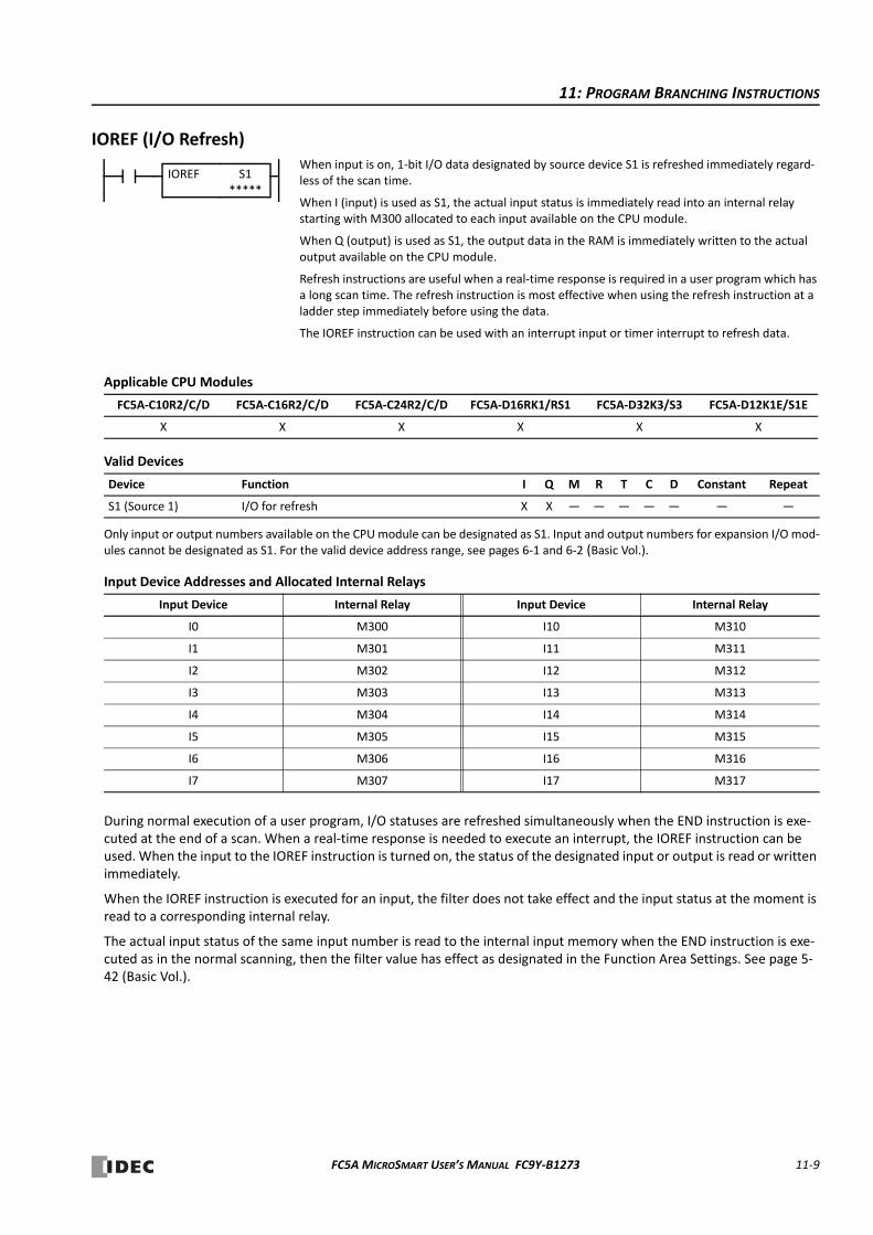
11: PROGRAM BRANCHING INSTRUCTIONS
IOREF (I/O Refresh)
Applicable CPU Modules
Valid Devices
Only input or output numbers available on the CPU module can be designated as S1. Input and output numbers for expansion I/O mod‐ules cannot be designated as S1. For the valid device address range, see pages 6‐1 and 6‐2 (Basic Vol.).
Input Device Addresses and Allocated Internal Relays
During normal execution of a user program, I/O statuses are refreshed simultaneously when the END instruction is exe‐cuted at the end of a scan. When a real‐time response is needed to execute an interrupt, the IOREF instruction can be used. When the input to the IOREF instruction is turned on, the status of the designated input or output is read or written immediately.
When the IOREF instruction is executed for an input, the filter does not take effect and the input status at the moment is read to a corresponding internal relay.
The actual input status of the same input number is read to the internal input memory when the END instruction is exe‐cuted as in the normal scanning, then the filter value has effect as designated in the Function Area Settings. See page 5‐42 (Basic Vol.).
FC5A‐C10R2/C/D FC5A‐C16R2/C/D FC5A‐C24R2/C/D FC5A‐D16RK1/RS1 FC5A‐D32K3/S3 FC5A‐D12K1E/S1E
X X X X X X
Device Function I Q M R T C D Constant Repeat
S1 (Source 1) I/O for refresh X X — — — — — — —
Input Device Internal Relay Input Device Internal Relay
I0 M300 I10 M310
I1 M301 I11 M311
I2 M302 I12 M312
I3 M303 I13 M313
I4 M304 I14 M314
I5 M305 I15 M315
I6 M306 I16 M316
I7 M307 I17 M317
When input is on, 1‐bit I/O data designated by source device S1 is refreshed immediately regard‐less of the scan time.
When I (input) is used as S1, the actual input status is immediately read into an internal relay starting with M300 allocated to each input available on the CPU module.
When Q (output) is used as S1, the output data in the RAM is immediately written to the actual output available on the CPU module.
Refresh instructions are useful when a real‐time response is required in a user program which has a long scan time. The refresh instruction is most effective when using the refresh instruction at a ladder step immediately before using the data.
The IOREF instruction can be used with an interrupt input or timer interrupt to refresh data.
IOREF S1*****
FC5A MICROSMART USER’S MANUAL FC9Y‐B1273 11‐9

11: PROGRAM BRANCHING INSTRUCTIONS
Example: IOREF
The following example demonstrates a program to transfer the input I0 status to output Q0 using the IOREF instruction. Input I2 is designated as an interrupt input. For the interrupt input function, see page 5‐34 (Basic Vol.).
M8120 is the initialize pulse special internal relay.
D8032 stores 0 to designate jump destination label 0 for interrupt input I2.
When input I2 is on, program execution jumps to label 0.
M8125 is the in‐operation output special internal relay.
IOREF immediately reads input I0 status to internal relay M300.
M300 turns on or off the output Q0 internal memory.
Another IOREF immediately writes the output Q0 internal memory status to actual output Q0.
Program execution returns to the main program.
M8120
END
Main Program
M8125
Q0
REPS1 –0
D1 –D8032
MOV(W)
IOREF S1I0
M300
M8125
IOREF S1Q0
LRET
LABEL0
11‐10 FC5A MICROSMART USER’S MANUAL FC9Y‐B1273
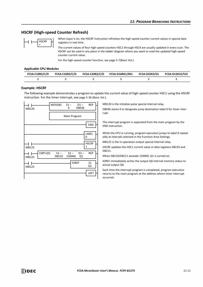
11: PROGRAM BRANCHING INSTRUCTIONS
HSCRF (High‐speed Counter Refresh)
Applicable CPU Modules
Example: HSCRF
The following example demonstrates a program to update the current value of high‐speed counter HSC1 using the HSCRF instruction. For the timer interrupt, see page 5‐36 (Basic Vol.).
FC5A‐C10R2/C/D FC5A‐C16R2/C/D FC5A‐C24R2/C/D FC5A‐D16RK1/RS1 FC5A‐D32K3/S3 FC5A‐D12K1E/S1E
X X X X X X
When input is on, the HSCRF instruction refreshes the high‐speed counter current values in special data registers in real time.
The current values of four high‐speed counters HSC1 through HSC4 are usually updated in every scan. The HSCRF can be used in any place in the ladder diagram where you want to read the updated high‐speed counter current value.
For the high‐speed counter function, see page 5‐7(Basic Vol.).
HSCRF*
M8120 is the initialize pulse special internal relay.
D8036 stores 0 to designate jump destination label 0 for timer inter‐rupt.
The interrupt program is separated from the main program by the END instruction.
While the CPU is running, program execution jumps to label 0 repeat‐edly at intervals selected in the Function Area Settings.
M8125 is the in‐operation output special internal relay.
HSCRF updates the HSC1 current value in data registers D8210 and D8211.
When D8210/D8211 exceeds 150000, Q1 is turned on.
IOREF immediately writes the output Q0 internal memory status to actual output Q0.
Each time the interrupt program is completed, program execution returns to the main program at the address where timer interrupt occurred.
M8120
END
Main Program
M8125
REPS1 –0
D1 –D8036
MOV(W)
M8125
M8125
IOREF S1Q1
LRET
LABEL0
HSCRF1
REPS1 –D8210
D1 –Q1
CMP>(D) S2 –150000
FC5A MICROSMART USER’S MANUAL FC9Y‐B1273 11‐11

11: PROGRAM BRANCHING INSTRUCTIONS
FRQRF (Frequency Measurement Refresh)
Applicable CPU Modules
Example: FRQRF
The following example demonstrates a program to update the current value of frequency measurement value using the FRQRF instruction. For the timer interrupt, see page 5‐36 (Basic Vol.).
FC5A‐C10R2/C/D FC5A‐C16R2/C/D FC5A‐C24R2/C/D FC5A‐D16RK1/RS1 FC5A‐D32K3/S3 FC5A‐D12K1E/S1E
X X X X X X
When input is on, the FRQRF instruction refreshes the frequency measurement values in special data reg‐isters in real time.
The FRQRF can be used in any place in the ladder diagram where you want to read the updated frequency measurement value.
Before the measured results are stored in the special data registers, it takes a maximum of calculation period plus one scan time. Using the FRQRF instruction in the ladder diagram, the latest value of the fre‐quency measurement can be read out within 250 ms regardless of the input frequency.
For the frequency measurement function, see page 5‐30 (Basic Vol.).
FRQRF*
M8120 is the initialize pulse special internal relay.
D8036 stores 0 to designate jump destination label 0 for timer inter‐rupt.
The interrupt program is separated from the main program by the END instruction.
While the CPU is running, program execution jumps to label 0 repeat‐edly at intervals selected in the Function Area Settings.
M8125 is the in‐operation output special internal relay.
FRQRF updates the HSC1 frequency measurement value in data regis‐ters D8060 and D8061.
When D8060/D8061 exceeds 5000, Q1 is turned on.
IOREF immediately writes the output Q0 internal memory status to actual output Q0.
Each time the interrupt program is completed, program execution returns to the main program at the address where timer interrupt occurred.
M8120
END
Main Program
M8125
REPS1 –0
D1 –D8036
MOV(W)
M8125
M8125
IOREF S1Q1
LRET
LABEL0
FRQRF1
REPS1 –D8060
D1 –Q1
CMP>(D) S2 –5000
11‐12 FC5A MICROSMART USER’S MANUAL FC9Y‐B1273
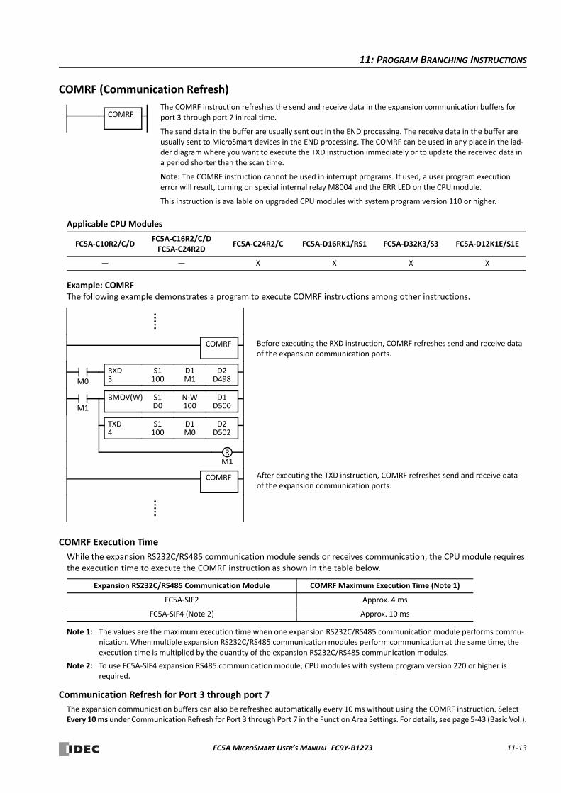
11: PROGRAM BRANCHING INSTRUCTIONS
COMRF (Communication Refresh)
Applicable CPU Modules
Example: COMRFThe following example demonstrates a program to execute COMRF instructions among other instructions.
COMRF Execution Time
While the expansion RS232C/RS485 communication module sends or receives communication, the CPU module requires the execution time to execute the COMRF instruction as shown in the table below.
Note 1: The values are the maximum execution time when one expansion RS232C/RS485 communication module performs commu‐nication. When multiple expansion RS232C/RS485 communication modules perform communication at the same time, the execution time is multiplied by the quantity of the expansion RS232C/RS485 communication modules.
Note 2: To use FC5A‐SIF4 expansion RS485 communication module, CPU modules with system program version 220 or higher is required.
Communication Refresh for Port 3 through port 7
The expansion communication buffers can also be refreshed automatically every 10 ms without using the COMRF instruction. Select Every 10 ms under Communication Refresh for Port 3 through Port 7 in the Function Area Settings. For details, see page 5‐43 (Basic Vol.).
FC5A‐C10R2/C/DFC5A‐C16R2/C/DFC5A‐C24R2D
FC5A‐C24R2/C FC5A‐D16RK1/RS1 FC5A‐D32K3/S3 FC5A‐D12K1E/S1E
— — X X X X
Expansion RS232C/RS485 Communication Module COMRF Maximum Execution Time (Note 1)
FC5A‐SIF2 Approx. 4 ms
FC5A‐SIF4 (Note 2) Approx. 10 ms
The COMRF instruction refreshes the send and receive data in the expansion communication buffers for port 3 through port 7 in real time.
The send data in the buffer are usually sent out in the END processing. The receive data in the buffer are usually sent to MicroSmart devices in the END processing. The COMRF can be used in any place in the lad‐der diagram where you want to execute the TXD instruction immediately or to update the received data in a period shorter than the scan time.
Note: The COMRF instruction cannot be used in interrupt programs. If used, a user program execution error will result, turning on special internal relay M8004 and the ERR LED on the CPU module.
This instruction is available on upgraded CPU modules with system program version 110 or higher.
COMRF
Before executing the RXD instruction, COMRF refreshes send and receive data of the expansion communication ports.
After executing the TXD instruction, COMRF refreshes send and receive data of the expansion communication ports.
M0
S1100
D1M1
RXD3
D2D498
M1
S1D0
N‐W100
BMOV(W) D1D500
COMRF
S1100
D1M0
TXD4
D2D502
COMRF
M1R
FC5A MICROSMART USER’S MANUAL FC9Y‐B1273 11‐13

11: PROGRAM BRANCHING INSTRUCTIONS
11‐14 FC5A MICROSMART USER’S MANUAL FC9Y‐B1273
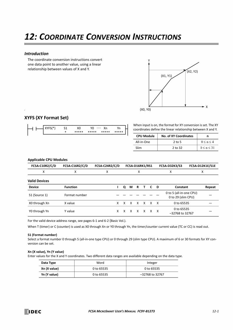
12: COORDINATE CONVERSION INSTRUCTIONS
IntroductionThe coordinate conversion instructions convert one data point to another value, using a linear relationship between values of X and Y.
⁄
XYFS (XY Format Set)
Applicable CPU Modules
Valid Devices
For the valid device address range, see pages 6‐1 and 6‐2 (Basic Vol.).
When T (timer) or C (counter) is used as X0 through Xn or Y0 through Yn, the timer/counter current value (TC or CC) is read out.
S1 (Format number)Select a format number 0 through 5 (all‐in‐one type CPU) or 0 through 29 (slim type CPU). A maximum of 6 or 30 formats for XY con‐version can be set.
Xn (X value), Yn (Y value)Enter values for the X and Y coordinates. Two different data ranges are available depending on the data type.
FC5A‐C10R2/C/D FC5A‐C16R2/C/D FC5A‐C24R2/C/D FC5A‐D16RK1/RS1 FC5A‐D32K3/S3 FC5A‐D12K1E/S1E
X X X X X X
Device Function I Q M R T C D Constant Repeat
S1 (Source 1) Format number — — — — — — —0 to 5 (all‐in‐one CPU)0 to 29 (slim CPU)
—
X0 through Xn X value X X X X X X X 0 to 65535 —
Y0 through Yn Y value X X X X X X X0 to 65535
–32768 to 32767—
Data Type Word Integer
Xn (X value) 0 to 65535 0 to 65535
Yn (Y value) 0 to 65535 –32768 to 32767
(X0, Y0)
(X1, Y1)(X2, Y2)
X
Y
When input is on, the format for XY conversion is set. The XY coordinates define the linear relationship between X and Y.
CPU Module No. of XY Coordinates n
All‐in‐One 2 to 5
Slim 2 to 32
0 n 4
0 n 31
XYFS(*) S1*
Y0*****
Xn*****
.....X0*****
Yn*****
FC5A MICROSMART USER’S MANUAL FC9Y‐B1273 12‐1
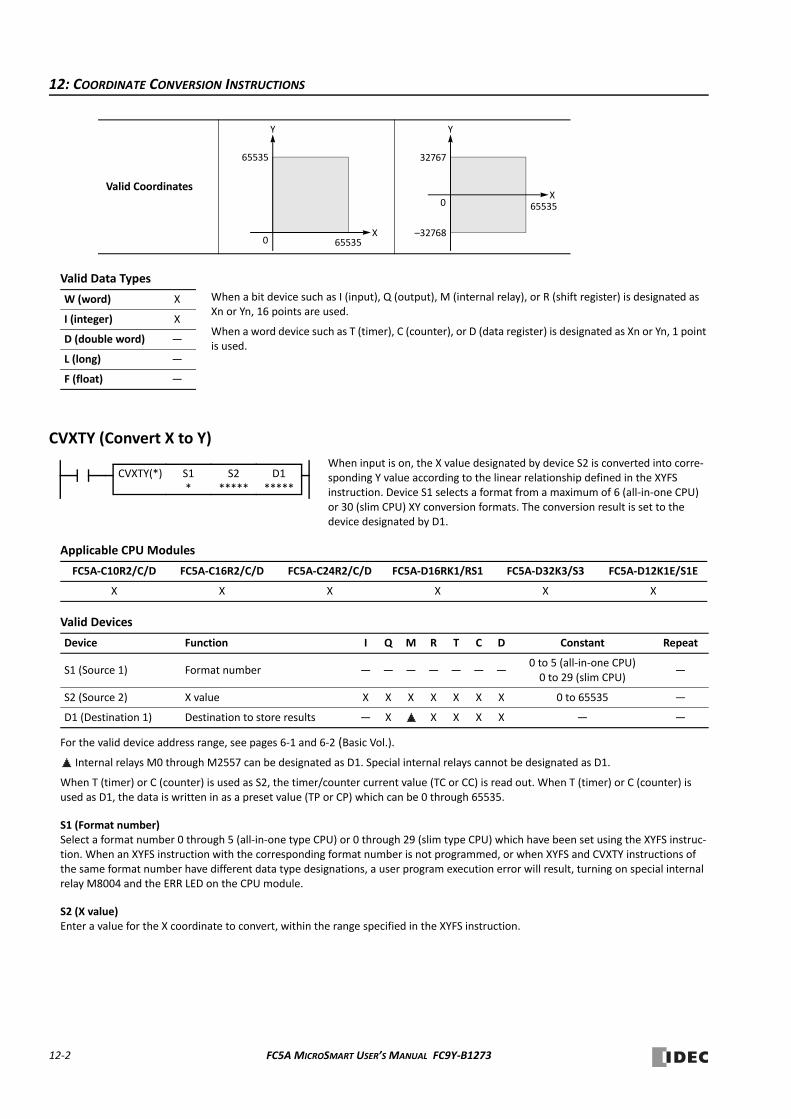
12: COORDINATE CONVERSION INSTRUCTIONS
Valid Data Types
CVXTY (Convert X to Y)
Applicable CPU Modules
Valid Devices
For the valid device address range, see pages 6‐1 and 6‐2 (Basic Vol.).
Internal relays M0 through M2557 can be designated as D1. Special internal relays cannot be designated as D1.
When T (timer) or C (counter) is used as S2, the timer/counter current value (TC or CC) is read out. When T (timer) or C (counter) is used as D1, the data is written in as a preset value (TP or CP) which can be 0 through 65535.
S1 (Format number)Select a format number 0 through 5 (all‐in‐one type CPU) or 0 through 29 (slim type CPU) which have been set using the XYFS instruc‐tion. When an XYFS instruction with the corresponding format number is not programmed, or when XYFS and CVXTY instructions of the same format number have different data type designations, a user program execution error will result, turning on special internal relay M8004 and the ERR LED on the CPU module.
S2 (X value)Enter a value for the X coordinate to convert, within the range specified in the XYFS instruction.
Valid Coordinates
W (word) X
I (integer) X
D (double word) —
L (long) —
F (float) —
FC5A‐C10R2/C/D FC5A‐C16R2/C/D FC5A‐C24R2/C/D FC5A‐D16RK1/RS1 FC5A‐D32K3/S3 FC5A‐D12K1E/S1E
X X X X X X
Device Function I Q M R T C D Constant Repeat
S1 (Source 1) Format number — — — — — — —0 to 5 (all‐in‐one CPU)0 to 29 (slim CPU)
—
S2 (Source 2) X value X X X X X X X 0 to 65535 —
D1 (Destination 1) Destination to store results — X X X X X — —
Y
0
65535
65535X
Y
0
32767
–32768
X65535
When a bit device such as I (input), Q (output), M (internal relay), or R (shift register) is designated as Xn or Yn, 16 points are used.
When a word device such as T (timer), C (counter), or D (data register) is designated as Xn or Yn, 1 point is used.
When input is on, the X value designated by device S2 is converted into corre‐sponding Y value according to the linear relationship defined in the XYFS instruction. Device S1 selects a format from a maximum of 6 (all‐in‐one CPU) or 30 (slim CPU) XY conversion formats. The conversion result is set to the device designated by D1.
CVXTY(*) S1*
S2*****
D1*****
12‐2 FC5A MICROSMART USER’S MANUAL FC9Y‐B1273
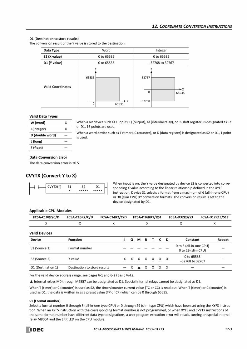
12: COORDINATE CONVERSION INSTRUCTIONS
D1 (Destination to store results)The conversion result of the Y value is stored to the destination.
Valid Data Types
Data Conversion Error
The data conversion error is ±0.5.
CVYTX (Convert Y to X)
Applicable CPU Modules
Valid Devices
For the valid device address range, see pages 6‐1 and 6‐2 (Basic Vol.).
Internal relays M0 through M2557 can be designated as D1. Special internal relays cannot be designated as D1.
When T (timer) or C (counter) is used as S2, the timer/counter current value (TC or CC) is read out. When T (timer) or C (counter) is used as D1, the data is written in as a preset value (TP or CP) which can be 0 through 65535.
S1 (Format number)Select a format number 0 through 5 (all‐in‐one type CPU) or 0 through 29 (slim type CPU) which have been set using the XYFS instruc‐tion. When an XYFS instruction with the corresponding format number is not programmed, or when XYFS and CVYTX instructions of the same format number have different data type designations, a user program execution error will result, turning on special internal relay M8004 and the ERR LED on the CPU module.
Data Type Word Integer
S2 (X value) 0 to 65535 0 to 65535
D1 (Y value) 0 to 65535 –32768 to 32767
Valid Coordinates
W (word) X
I (integer) X
D (double word) —
L (long) —
F (float) —
FC5A‐C10R2/C/D FC5A‐C16R2/C/D FC5A‐C24R2/C/D FC5A‐D16RK1/RS1 FC5A‐D32K3/S3 FC5A‐D12K1E/S1E
X X X X X X
Device Function I Q M R T C D Constant Repeat
S1 (Source 1) Format number — — — — — — —0 to 5 (all‐in‐one CPU)0 to 29 (slim CPU)
—
S2 (Source 2) Y value X X X X X X X0 to 65535
–32768 to 32767—
D1 (Destination 1) Destination to store results — X X X X X — —
Y
0
65535
65535X
Y
0
32767
–32768
X65535
When a bit device such as I (input), Q (output), M (internal relay), or R (shift register) is designated as S2 or D1, 16 points are used.
When a word device such as T (timer), C (counter), or D (data register) is designated as S2 or D1, 1 point is used.
When input is on, the Y value designated by device S2 is converted into corre‐sponding X value according to the linear relationship defined in the XYFS instruction. Device S1 selects a format from a maximum of 6 (all‐in‐one CPU) or 30 (slim CPU) XY conversion formats. The conversion result is set to the device designated by D1.
CVYTX(*) S1*
S2*****
D1*****
FC5A MICROSMART USER’S MANUAL FC9Y‐B1273 12‐3
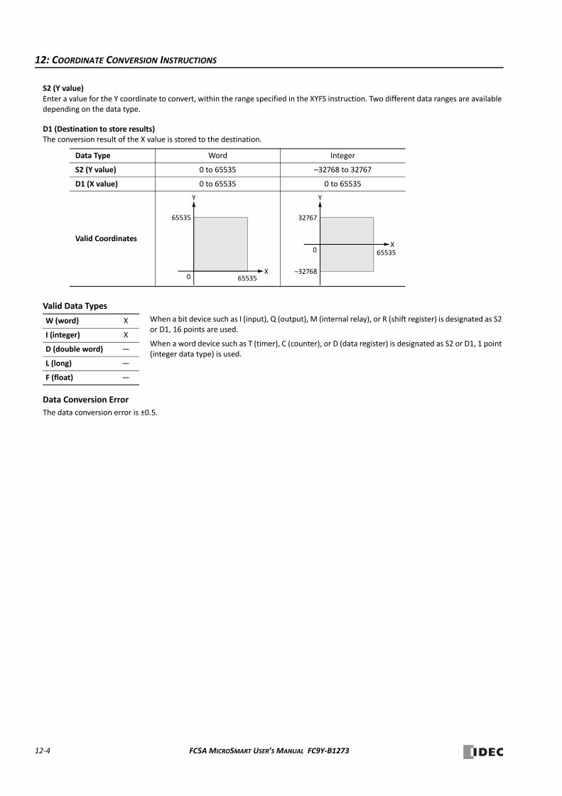
12: COORDINATE CONVERSION INSTRUCTIONS
S2 (Y value)Enter a value for the Y coordinate to convert, within the range specified in the XYFS instruction. Two different data ranges are available depending on the data type.
D1 (Destination to store results)The conversion result of the X value is stored to the destination.
Valid Data Types
Data Conversion Error
The data conversion error is ±0.5.
Data Type Word Integer
S2 (Y value) 0 to 65535 –32768 to 32767
D1 (X value) 0 to 65535 0 to 65535
Valid Coordinates
W (word) X
I (integer) X
D (double word) —
L (long) —
F (float) —
Y
0
65535
65535X
Y
0
32767
–32768
X65535
When a bit device such as I (input), Q (output), M (internal relay), or R (shift register) is designated as S2 or D1, 16 points are used.
When a word device such as T (timer), C (counter), or D (data register) is designated as S2 or D1, 1 point (integer data type) is used.
12‐4 FC5A MICROSMART USER’S MANUAL FC9Y‐B1273
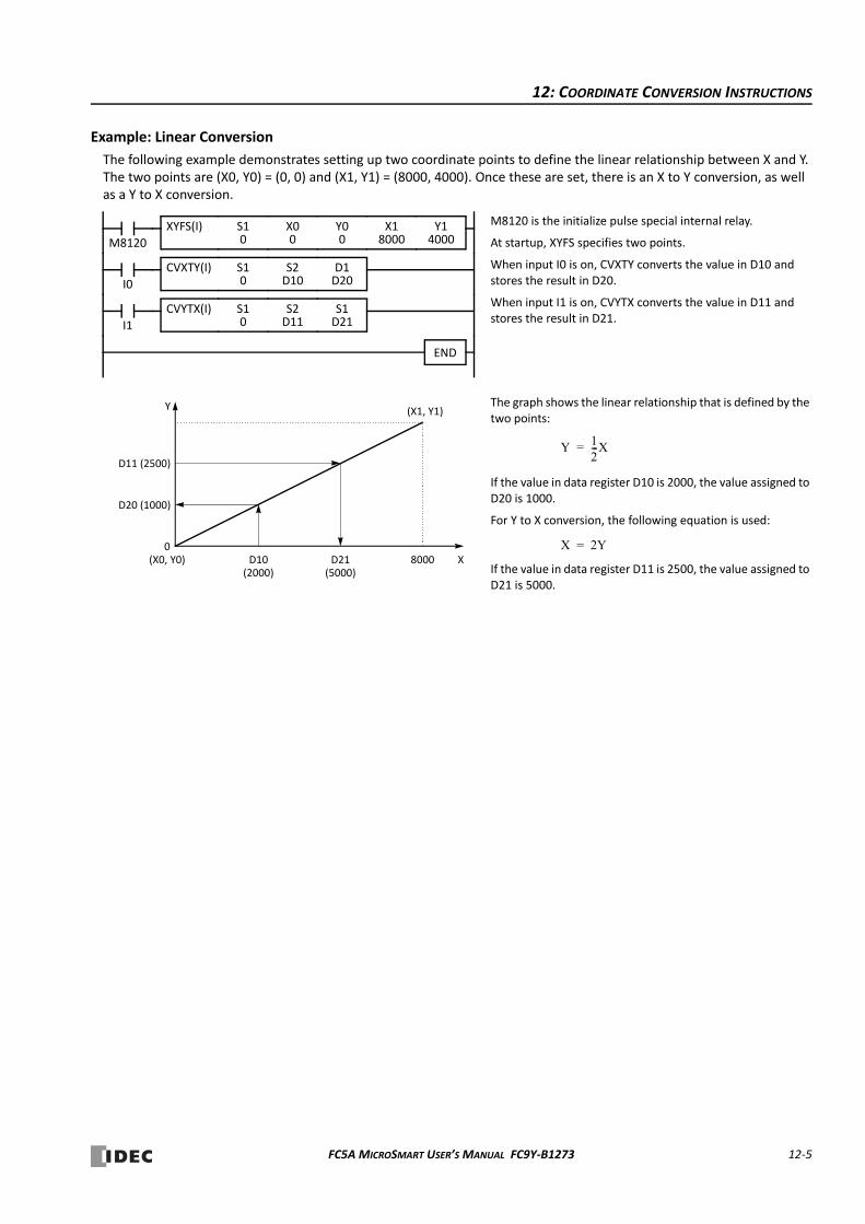
12: COORDINATE CONVERSION INSTRUCTIONS
Example: Linear Conversion
The following example demonstrates setting up two coordinate points to define the linear relationship between X and Y. The two points are (X0, Y0) = (0, 0) and (X1, Y1) = (8000, 4000). Once these are set, there is an X to Y conversion, as well as a Y to X conversion.
M8120 is the initialize pulse special internal relay.
At startup, XYFS specifies two points.
When input I0 is on, CVXTY converts the value in D10 and stores the result in D20.
When input I1 is on, CVYTX converts the value in D11 and stores the result in D21.
M8120
XYFS(I) Y14000
END
I0
CVXTY(I) D1D20
I1
CVYTX(I) S1D21
S10
X00
Y00
X18000
S10
S2D10
S10
S2D11
(X0, Y0)
(X1, Y1)
X
Y
0D10 D21
D20 (1000)
D11 (2500)
The graph shows the linear relationship that is defined by the two points:
If the value in data register D10 is 2000, the value assigned to D20 is 1000.
For Y to X conversion, the following equation is used:
If the value in data register D11 is 2500, the value assigned to D21 is 5000.
Y 12---X=
X 2Y=8000
(2000) (5000)
FC5A MICROSMART USER’S MANUAL FC9Y‐B1273 12‐5
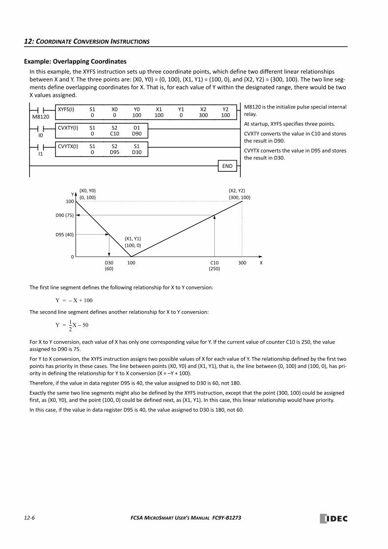
12: COORDINATE CONVERSION INSTRUCTIONS
Example: Overlapping Coordinates
In this example, the XYFS instruction sets up three coordinate points, which define two different linear relationships between X and Y. The three points are: (X0, Y0) = (0, 100), (X1, Y1) = (100, 0), and (X2, Y2) = (300, 100). The two line seg‐ments define overlapping coordinates for X. That is, for each value of Y within the designated range, there would be two X values assigned.
The first line segment defines the following relationship for X to Y conversion:
The second line segment defines another relationship for X to Y conversion:
For X to Y conversion, each value of X has only one corresponding value for Y. If the current value of counter C10 is 250, the value assigned to D90 is 75.
For Y to X conversion, the XYFS instruction assigns two possible values of X for each value of Y. The relationship defined by the first two points has priority in these cases. The line between points (X0, Y0) and (X1, Y1), that is, the line between (0, 100) and (100, 0), has pri‐ority in defining the relationship for Y to X conversion (X = –Y + 100).
Therefore, if the value in data register D95 is 40, the value assigned to D30 is 60, not 180.
Exactly the same two line segments might also be defined by the XYFS instruction, except that the point (300, 100) could be assigned first, as (X0, Y0), and the point (100, 0) could be defined next, as (X1, Y1). In this case, this linear relationship would have priority.
In this case, if the value in data register D95 is 40, the value assigned to D30 is 180, not 60.
M8120 is the initialize pulse special internal relay.
At startup, XYFS specifies three points.
CVXTY converts the value in C10 and stores the result in D90.
CVYTX converts the value in D95 and stores the result in D30.
M8120
XYFS(I) Y2100
END
I0
CVXTY(I) D1D90
I1
CVYTX(I) S1D30
S10
X00
Y0100
X1100
S10
S2C10
S10
S2D95
X
Y
0D30 C10
D95 (40)
D90 (75)
300
Y10
X2300
100
(X0, Y0)
(0, 100)
(X1, Y1)
(100, 0)
(X2, Y2)
(300, 100)
100(60) (250)
Y X– 100+=
Y 12---X 50–=
12‐6 FC5A MICROSMART USER’S MANUAL FC9Y‐B1273
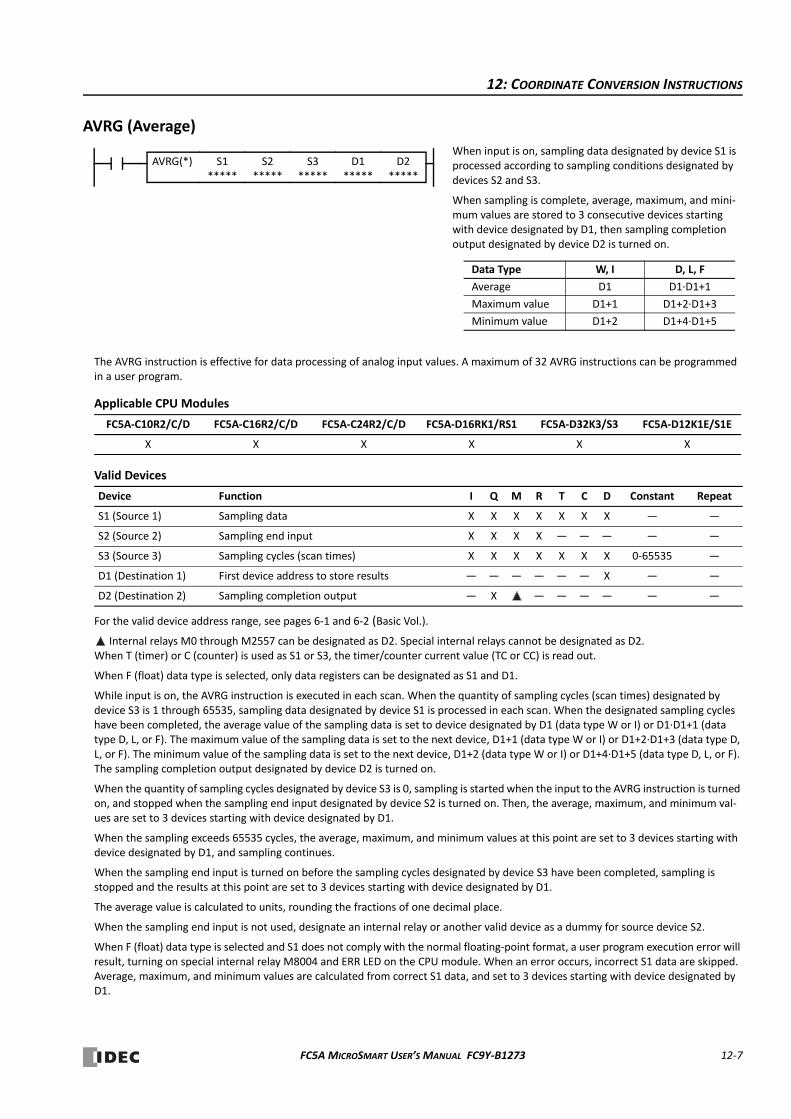
12: COORDINATE CONVERSION INSTRUCTIONS
AVRG (Average)
The AVRG instruction is effective for data processing of analog input values. A maximum of 32 AVRG instructions can be programmed in a user program.
Applicable CPU Modules
Valid Devices
For the valid device address range, see pages 6‐1 and 6‐2 (Basic Vol.).
Internal relays M0 through M2557 can be designated as D2. Special internal relays cannot be designated as D2.When T (timer) or C (counter) is used as S1 or S3, the timer/counter current value (TC or CC) is read out.
When F (float) data type is selected, only data registers can be designated as S1 and D1.
While input is on, the AVRG instruction is executed in each scan. When the quantity of sampling cycles (scan times) designated by device S3 is 1 through 65535, sampling data designated by device S1 is processed in each scan. When the designated sampling cycles have been completed, the average value of the sampling data is set to device designated by D1 (data type W or I) or D1∙D1+1 (data type D, L, or F). The maximum value of the sampling data is set to the next device, D1+1 (data type W or I) or D1+2∙D1+3 (data type D, L, or F). The minimum value of the sampling data is set to the next device, D1+2 (data type W or I) or D1+4∙D1+5 (data type D, L, or F). The sampling completion output designated by device D2 is turned on.
When the quantity of sampling cycles designated by device S3 is 0, sampling is started when the input to the AVRG instruction is turned on, and stopped when the sampling end input designated by device S2 is turned on. Then, the average, maximum, and minimum val‐ues are set to 3 devices starting with device designated by D1.
When the sampling exceeds 65535 cycles, the average, maximum, and minimum values at this point are set to 3 devices starting with device designated by D1, and sampling continues.
When the sampling end input is turned on before the sampling cycles designated by device S3 have been completed, sampling is stopped and the results at this point are set to 3 devices starting with device designated by D1.
The average value is calculated to units, rounding the fractions of one decimal place.
When the sampling end input is not used, designate an internal relay or another valid device as a dummy for source device S2.
When F (float) data type is selected and S1 does not comply with the normal floating‐point format, a user program execution error will result, turning on special internal relay M8004 and ERR LED on the CPU module. When an error occurs, incorrect S1 data are skipped. Average, maximum, and minimum values are calculated from correct S1 data, and set to 3 devices starting with device designated by D1.
FC5A‐C10R2/C/D FC5A‐C16R2/C/D FC5A‐C24R2/C/D FC5A‐D16RK1/RS1 FC5A‐D32K3/S3 FC5A‐D12K1E/S1E
X X X X X X
Device Function I Q M R T C D Constant Repeat
S1 (Source 1) Sampling data X X X X X X X — —
S2 (Source 2) Sampling end input X X X X — — — — —
S3 (Source 3) Sampling cycles (scan times) X X X X X X X 0‐65535 —
D1 (Destination 1) First device address to store results — — — — — — X — —
D2 (Destination 2) Sampling completion output — X — — — — — —
When input is on, sampling data designated by device S1 is processed according to sampling conditions designated by devices S2 and S3.
When sampling is complete, average, maximum, and mini‐mum values are stored to 3 consecutive devices starting with device designated by D1, then sampling completion output designated by device D2 is turned on.
Data Type W, I D, L, F
Average D1 D1∙D1+1
Maximum value D1+1 D1+2∙D1+3
Minimum value D1+2 D1+4∙D1+5
AVRG(*) S1*****
S3*****
D1*****
S2*****
D2*****
FC5A MICROSMART USER’S MANUAL FC9Y‐B1273 12‐7

12: COORDINATE CONVERSION INSTRUCTIONS
Valid Data Types
Example: AVRG
The following example demonstrates a program to calculate average values of the data register D100 and store the result to data register D200 in every 500 scans.
When the sampling end input does not turn on
While sampling end input I10 is off, the average, maximum, and minimum values are calculated in every 500 scans and stored to data registers D200, D201, and D202, respectively. Sampling completion output M100 is set every 500 scans.
When the sampling end input turns on
When sampling end input I10 turns on, the average, maximum, and minimum values at this point are stored to data reg‐isters D200, D201, and D202, respectively. Sampling completion output M100 is also set. When sampling end input I10 turns off, sampling resumes starting at the first scan.
W (word) X
I (integer) X
D (double word) X
L (long) X
F (float) X
When a bit device such as I (input), Q (output), M (internal relay), or R (shift register) is designated as the source, 16 points (word or integer data type) or 32 points (double‐word or long data type) are used.
When a word device such as T (timer), C (counter), or D (data register) is designated as the source, 1 point (word or integer data type) or 2 points (double‐word, long, or float data type) are used.
M8125 is the in‐operation output special internal relay.
M8125
S1D100
S2I10
AVRG(W) D2M100
S3500
D1D200
512
1st scan
497
2nd scan
521
500th scan
499
1st scan
478
2nd scan
In‐operation Special IR M8125ON
OFF
Sampling End Input I10ON
OFF
Sampling Completion Output M100ON
OFF
Sampling Data D100
Average Value D200 500
Maximum Value D201 530
Minimum Value D202 480
Values are set every 500 scans.
489
151st scan
510
152nd scan
509
153rd scan
504
XXXth scan
493
1st scan
In‐operation Special IR M8125ON
OFF
Sampling End Input I10ON
OFF
Sampling Completion Output M100ON
OFF
Sampling Data D100
Average Value D200 502
Maximum Value D201 513
Minimum Value D202 485
Values are set when I10 is turned on.
12‐8 FC5A MICROSMART USER’S MANUAL FC9Y‐B1273
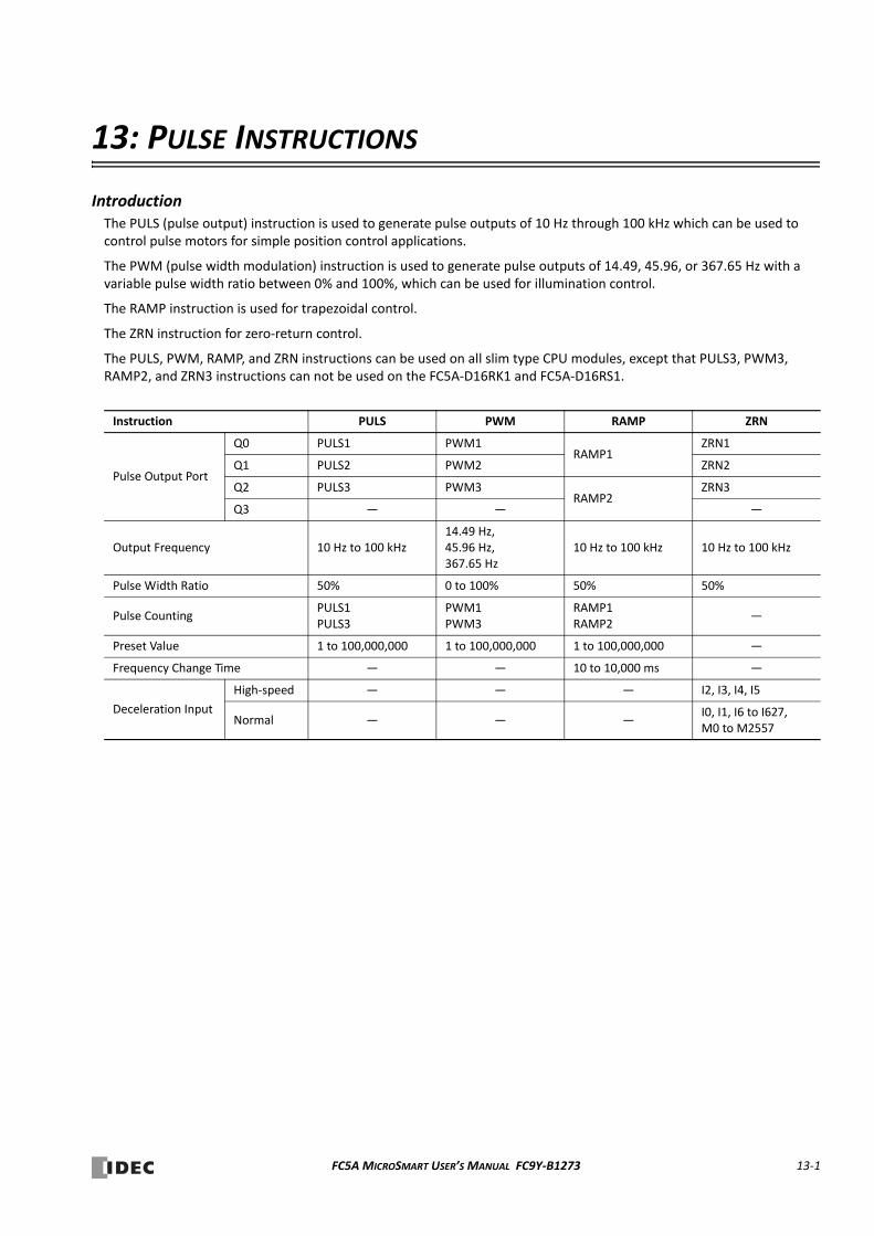
13: PULSE INSTRUCTIONS
IntroductionThe PULS (pulse output) instruction is used to generate pulse outputs of 10 Hz through 100 kHz which can be used to control pulse motors for simple position control applications.
The PWM (pulse width modulation) instruction is used to generate pulse outputs of 14.49, 45.96, or 367.65 Hz with a variable pulse width ratio between 0% and 100%, which can be used for illumination control.
The RAMP instruction is used for trapezoidal control.
The ZRN instruction for zero‐return control.
The PULS, PWM, RAMP, and ZRN instructions can be used on all slim type CPU modules, except that PULS3, PWM3, RAMP2, and ZRN3 instructions can not be used on the FC5A‐D16RK1 and FC5A‐D16RS1.
Instruction PULS PWM RAMP ZRN
Pulse Output Port
Q0 PULS1 PWM1RAMP1
ZRN1
Q1 PULS2 PWM2 ZRN2
Q2 PULS3 PWM3RAMP2
ZRN3
Q3 — — —
Output Frequency 10 Hz to 100 kHz14.49 Hz, 45.96 Hz, 367.65 Hz
10 Hz to 100 kHz 10 Hz to 100 kHz
Pulse Width Ratio 50% 0 to 100% 50% 50%
Pulse CountingPULS1PULS3
PWM1PWM3
RAMP1RAMP2
—
Preset Value 1 to 100,000,000 1 to 100,000,000 1 to 100,000,000 —
Frequency Change Time — — 10 to 10,000 ms —
Deceleration Input
High‐speed — — — I2, I3, I4, I5
Normal — — —I0, I1, I6 to I627, M0 to M2557
FC5A MICROSMART USER’S MANUAL FC9Y‐B1273 13‐1
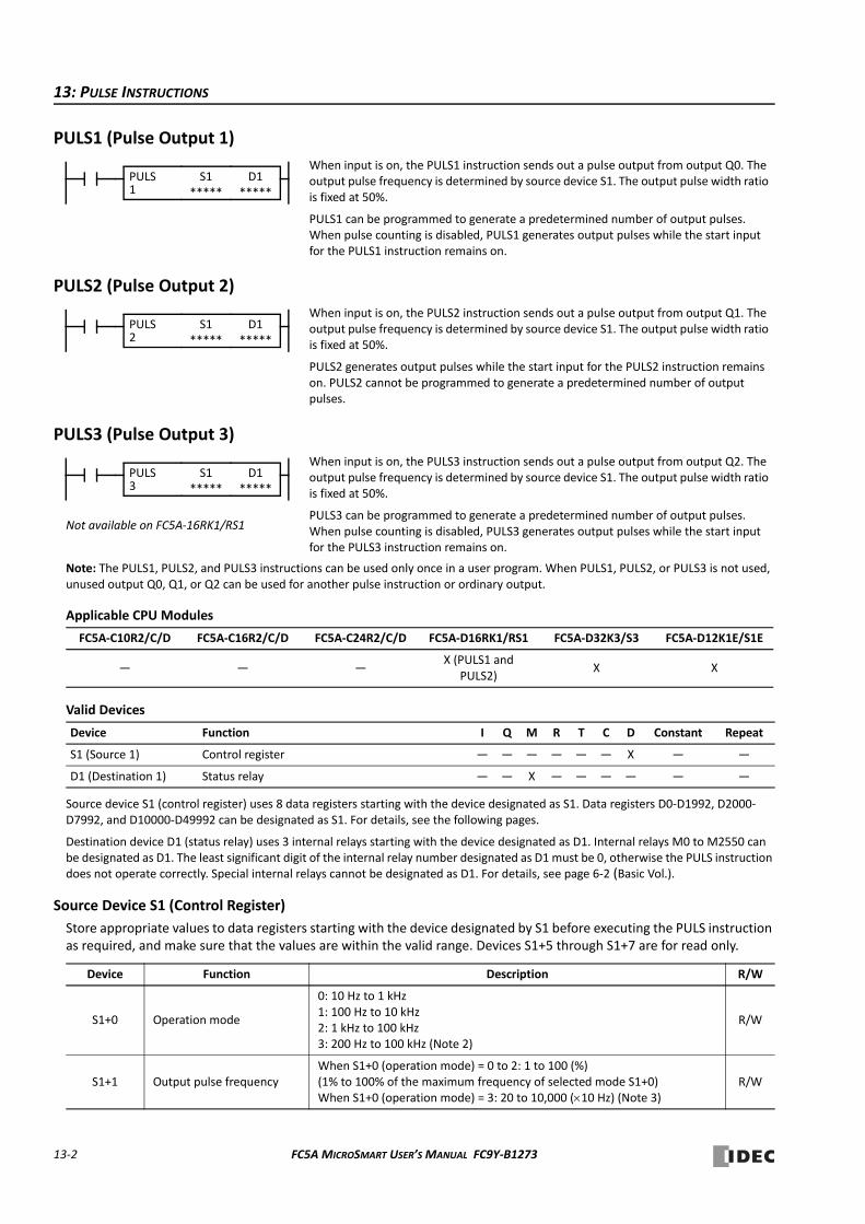
13: PULSE INSTRUCTIONS
PULS1 (Pulse Output 1)
PULS2 (Pulse Output 2)
PULS3 (Pulse Output 3)
Note: The PULS1, PULS2, and PULS3 instructions can be used only once in a user program. When PULS1, PULS2, or PULS3 is not used, unused output Q0, Q1, or Q2 can be used for another pulse instruction or ordinary output.
Applicable CPU Modules
Valid Devices
Source device S1 (control register) uses 8 data registers starting with the device designated as S1. Data registers D0‐D1992, D2000‐D7992, and D10000‐D49992 can be designated as S1. For details, see the following pages.
Destination device D1 (status relay) uses 3 internal relays starting with the device designated as D1. Internal relays M0 to M2550 can be designated as D1. The least significant digit of the internal relay number designated as D1 must be 0, otherwise the PULS instruction does not operate correctly. Special internal relays cannot be designated as D1. For details, see page 6‐2 (Basic Vol.).
Source Device S1 (Control Register)
Store appropriate values to data registers starting with the device designated by S1 before executing the PULS instruction as required, and make sure that the values are within the valid range. Devices S1+5 through S1+7 are for read only.
FC5A‐C10R2/C/D FC5A‐C16R2/C/D FC5A‐C24R2/C/D FC5A‐D16RK1/RS1 FC5A‐D32K3/S3 FC5A‐D12K1E/S1E
— — —X (PULS1 and
PULS2)X X
Device Function I Q M R T C D Constant Repeat
S1 (Source 1) Control register — — — — — — X — —
D1 (Destination 1) Status relay — — X — — — — — —
Device Function Description R/W
S1+0 Operation mode
0: 10 Hz to 1 kHz1: 100 Hz to 10 kHz2: 1 kHz to 100 kHz3: 200 Hz to 100 kHz (Note 2)
R/W
S1+1 Output pulse frequencyWhen S1+0 (operation mode) = 0 to 2: 1 to 100 (%)(1% to 100% of the maximum frequency of selected mode S1+0)When S1+0 (operation mode) = 3: 20 to 10,000 (10 Hz) (Note 3)
R/W
When input is on, the PULS1 instruction sends out a pulse output from output Q0. The output pulse frequency is determined by source device S1. The output pulse width ratio is fixed at 50%.
PULS1 can be programmed to generate a predetermined number of output pulses. When pulse counting is disabled, PULS1 generates output pulses while the start input for the PULS1 instruction remains on.
PULS1
S1*****
D1*****
When input is on, the PULS2 instruction sends out a pulse output from output Q1. The output pulse frequency is determined by source device S1. The output pulse width ratio is fixed at 50%.
PULS2 generates output pulses while the start input for the PULS2 instruction remains on. PULS2 cannot be programmed to generate a predetermined number of output pulses.
PULS2
S1*****
D1*****
When input is on, the PULS3 instruction sends out a pulse output from output Q2. The output pulse frequency is determined by source device S1. The output pulse width ratio is fixed at 50%.
PULS3 can be programmed to generate a predetermined number of output pulses. When pulse counting is disabled, PULS3 generates output pulses while the start input for the PULS3 instruction remains on.
PULS3
S1*****
D1*****
Not available on FC5A‐16RK1/RS1
13‐2 FC5A MICROSMART USER’S MANUAL FC9Y‐B1273
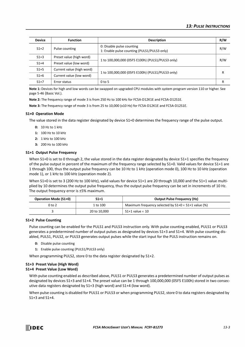
13: PULSE INSTRUCTIONS
Note 1: Devices for high and low words can be swapped on upgraded CPU modules with system program version 110 or higher. See page 5‐46 (Basic Vol.).
Note 2: The frequency range of mode 3 is from 250 Hz to 100 kHz for FC5A‐D12K1E and FC5A‐D12S1E.
Note 3: The frequency range of mode 3 is from 25 to 10,000 (x10 Hz) for FC5A‐D12K1E and FC5A‐D12S1E.
S1+0 Operation Mode
The value stored in the data register designated by device S1+0 determines the frequency range of the pulse output.
0: 10 Hz to 1 kHz
1: 100 Hz to 10 kHz
2: 1 kHz to 100 kHz
3: 200 Hz to 100 kHz
S1+1 Output Pulse Frequency
When S1+0 is set to 0 through 2, the value stored in the data register designated by device S1+1 specifies the frequency of the pulse output in percent of the maximum of the frequency range selected by S1+0. Valid values for device S1+1 are 1 through 100, thus the output pulse frequency can be 10 Hz to 1 kHz (operation mode 0), 100 Hz to 10 kHz (operation mode 1), or 1 kHz to 100 kHz (operation mode 2).
When S1+0 is set to 3 (200 Hz to 100 kHz), valid values for device S1+1 are 20 through 10,000 and the S1+1 value multi‐plied by 10 determines the output pulse frequency, thus the output pulse frequency can be set in increments of 10 Hz. The output frequency error is ±5% maximum.
S1+2 Pulse Counting
Pulse counting can be enabled for the PULS1 and PULS3 instruction only. With pulse counting enabled, PULS1 or PULS3 generates a predetermined number of output pulses as designated by devices S1+3 and S1+4. With pulse counting dis‐abled, PULS1, PULS2, or PULS3 generates output pulses while the start input for the PULS instruction remains on.
0: Disable pulse counting
1: Enable pulse counting (PULS1/PULS3 only)
When programming PULS2, store 0 to the data register designated by S1+2.
S1+3 Preset Value (High Word)S1+4 Preset Value (Low Word)
With pulse counting enabled as described above, PULS1 or PULS3 generates a predetermined number of output pulses as designated by devices S1+3 and S1+4. The preset value can be 1 through 100,000,000 (05F5 E100h) stored in two consec‐utive data registers designated by S1+3 (high word) and S1+4 (low word).
When pulse counting is disabled for PULS1 or PULS3 or when programming PULS2, store 0 to data registers designated by S1+3 and S1+4.
S1+2 Pulse counting0: Disable pulse counting1: Enable pulse counting (PULS1/PULS3 only)
R/W
S1+3 Preset value (high word)1 to 100,000,000 (05F5 E100h) (PULS1/PULS3 only) R/W
S1+4 Preset value (low word)
S1+5 Current value (high word)1 to 100,000,000 (05F5 E100h) (PULS1/PULS3 only) R
S1+6 Current value (low word)
S1+7 Error status 0 to 5 R
Operation Mode (S1+0) S1+1 Output Pulse Frequency (Hz)
0 to 2 1 to 100 Maximum frequency selected by S1+0 S1+1 value (%)
3 20 to 10,000 S1+1 value 10
Device Function Description R/W
FC5A MICROSMART USER’S MANUAL FC9Y‐B1273 13‐3
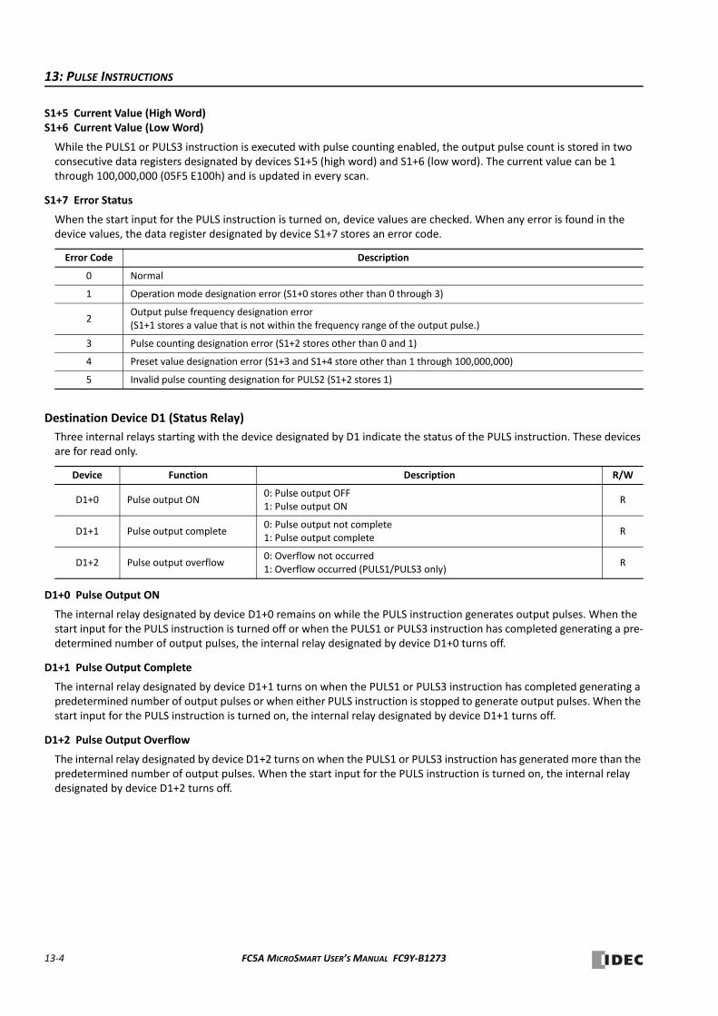
13: PULSE INSTRUCTIONS
S1+5 Current Value (High Word)S1+6 Current Value (Low Word)
While the PULS1 or PULS3 instruction is executed with pulse counting enabled, the output pulse count is stored in two consecutive data registers designated by devices S1+5 (high word) and S1+6 (low word). The current value can be 1 through 100,000,000 (05F5 E100h) and is updated in every scan.
S1+7 Error Status
When the start input for the PULS instruction is turned on, device values are checked. When any error is found in the device values, the data register designated by device S1+7 stores an error code.
Destination Device D1 (Status Relay)
Three internal relays starting with the device designated by D1 indicate the status of the PULS instruction. These devices are for read only.
D1+0 Pulse Output ON
The internal relay designated by device D1+0 remains on while the PULS instruction generates output pulses. When the start input for the PULS instruction is turned off or when the PULS1 or PULS3 instruction has completed generating a pre‐determined number of output pulses, the internal relay designated by device D1+0 turns off.
D1+1 Pulse Output Complete
The internal relay designated by device D1+1 turns on when the PULS1 or PULS3 instruction has completed generating a predetermined number of output pulses or when either PULS instruction is stopped to generate output pulses. When the start input for the PULS instruction is turned on, the internal relay designated by device D1+1 turns off.
D1+2 Pulse Output Overflow
The internal relay designated by device D1+2 turns on when the PULS1 or PULS3 instruction has generated more than the predetermined number of output pulses. When the start input for the PULS instruction is turned on, the internal relay designated by device D1+2 turns off.
Error Code Description
0 Normal
1 Operation mode designation error (S1+0 stores other than 0 through 3)
2Output pulse frequency designation error (S1+1 stores a value that is not within the frequency range of the output pulse.)
3 Pulse counting designation error (S1+2 stores other than 0 and 1)
4 Preset value designation error (S1+3 and S1+4 store other than 1 through 100,000,000)
5 Invalid pulse counting designation for PULS2 (S1+2 stores 1)
Device Function Description R/W
D1+0 Pulse output ON0: Pulse output OFF1: Pulse output ON
R
D1+1 Pulse output complete0: Pulse output not complete1: Pulse output complete
R
D1+2 Pulse output overflow0: Overflow not occurred1: Overflow occurred (PULS1/PULS3 only)
R
13‐4 FC5A MICROSMART USER’S MANUAL FC9Y‐B1273
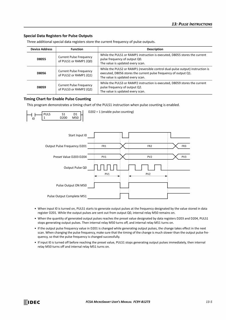
13: PULSE INSTRUCTIONS
Special Data Registers for Pulse Outputs
Three additional special data registers store the current frequency of pulse outputs.
Timing Chart for Enable Pulse Counting
This program demonstrates a timing chart of the PULS1 instruction when pulse counting is enabled.
Device Address Function Description
D8055Current Pulse Frequency of PULS1 or RAMP1 (Q0)
While the PULS1 or RAMP1 instruction is executed, D8055 stores the current pulse frequency of output Q0. The value is updated every scan.
D8056Current Pulse Frequency of PULS2 or RAMP1 (Q1)
While the PULS2 or RAMP1 (reversible control dual‐pulse output) instruction is executed, D8056 stores the current pulse frequency of output Q1. The value is updated every scan.
D8059Current Pulse Frequency of PULS3 or RAMP2 (Q2)
While the PULS3 or RAMP2 instruction is executed, D8059 stores the current pulse frequency of output Q2. The value is updated every scan.
D1M50I0
PULS1
S1D200
D202 = 1 (enable pulse counting)
Output Pulse Q0
Output Pulse Frequency D201
PV1
FR1
Start Input I0
• When input I0 is turned on, PULS1 starts to generate output pulses at the frequency designated by the value stored in data register D201. While the output pulses are sent out from output Q0, internal relay M50 remains on.
• When the quantity of generated output pulses reaches the preset value designated by data registers D203 and D204, PULS1 stops generating output pulses. Then internal relay M50 turns off, and internal relay M51 turns on.
• If the output pulse frequency value in D201 is changed while generating output pulses, the change takes effect in the next scan. When changing the pulse frequency, make sure that the timing of the change is much slower than the output pulse fre‐quency, so that the pulse frequency is changed successfully.
• If input I0 is turned off before reaching the preset value, PULS1 stops generating output pulses immediately, then internal relay M50 turns off and internal relay M51 turns on.
FR2 FR3
Preset Value D203∙D204 PV1 PV2 PV3
Pulse Output ON M50
Pulse Output Complete M51
PV2
FC5A MICROSMART USER’S MANUAL FC9Y‐B1273 13‐5
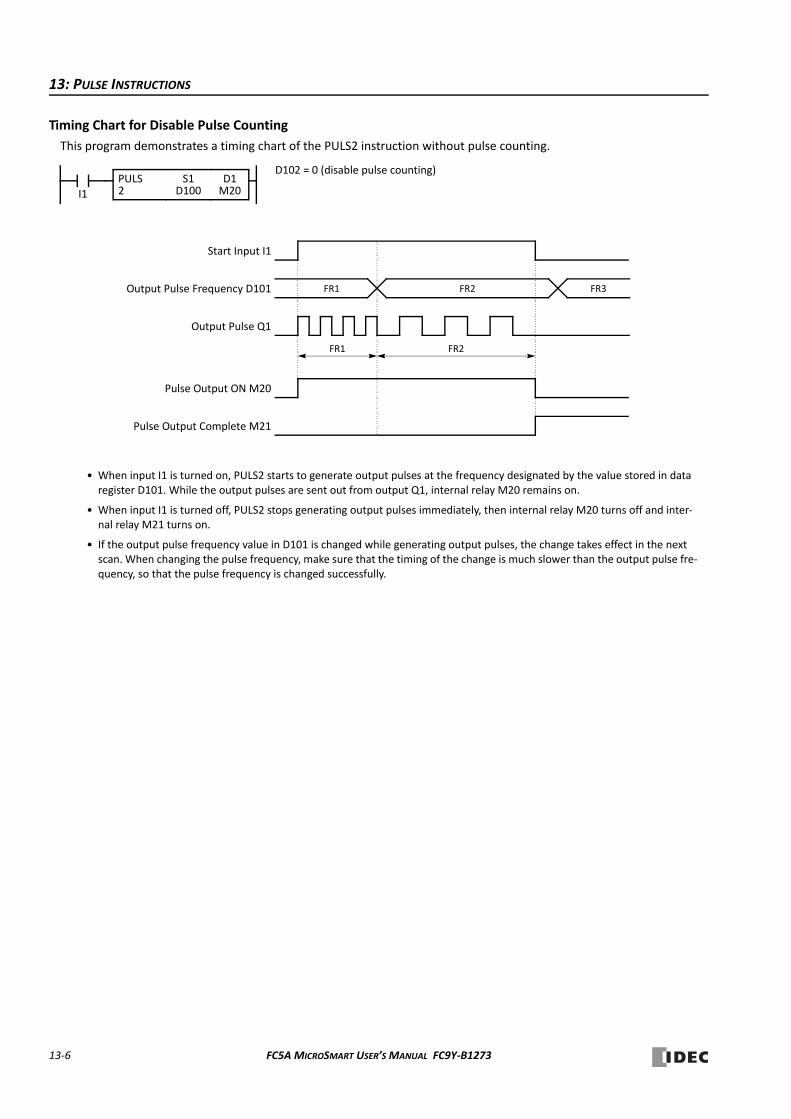
13: PULSE INSTRUCTIONS
Timing Chart for Disable Pulse Counting
This program demonstrates a timing chart of the PULS2 instruction without pulse counting.
D1M20I1
PULS2
S1D100
D102 = 0 (disable pulse counting)
Output Pulse Q1
Output Pulse Frequency D101
FR1
FR1
Start Input I1
• When input I1 is turned on, PULS2 starts to generate output pulses at the frequency designated by the value stored in data register D101. While the output pulses are sent out from output Q1, internal relay M20 remains on.
• When input I1 is turned off, PULS2 stops generating output pulses immediately, then internal relay M20 turns off and inter‐nal relay M21 turns on.
• If the output pulse frequency value in D101 is changed while generating output pulses, the change takes effect in the next scan. When changing the pulse frequency, make sure that the timing of the change is much slower than the output pulse fre‐quency, so that the pulse frequency is changed successfully.
FR2 FR3
Pulse Output ON M20
Pulse Output Complete M21
FR2
13‐6 FC5A MICROSMART USER’S MANUAL FC9Y‐B1273
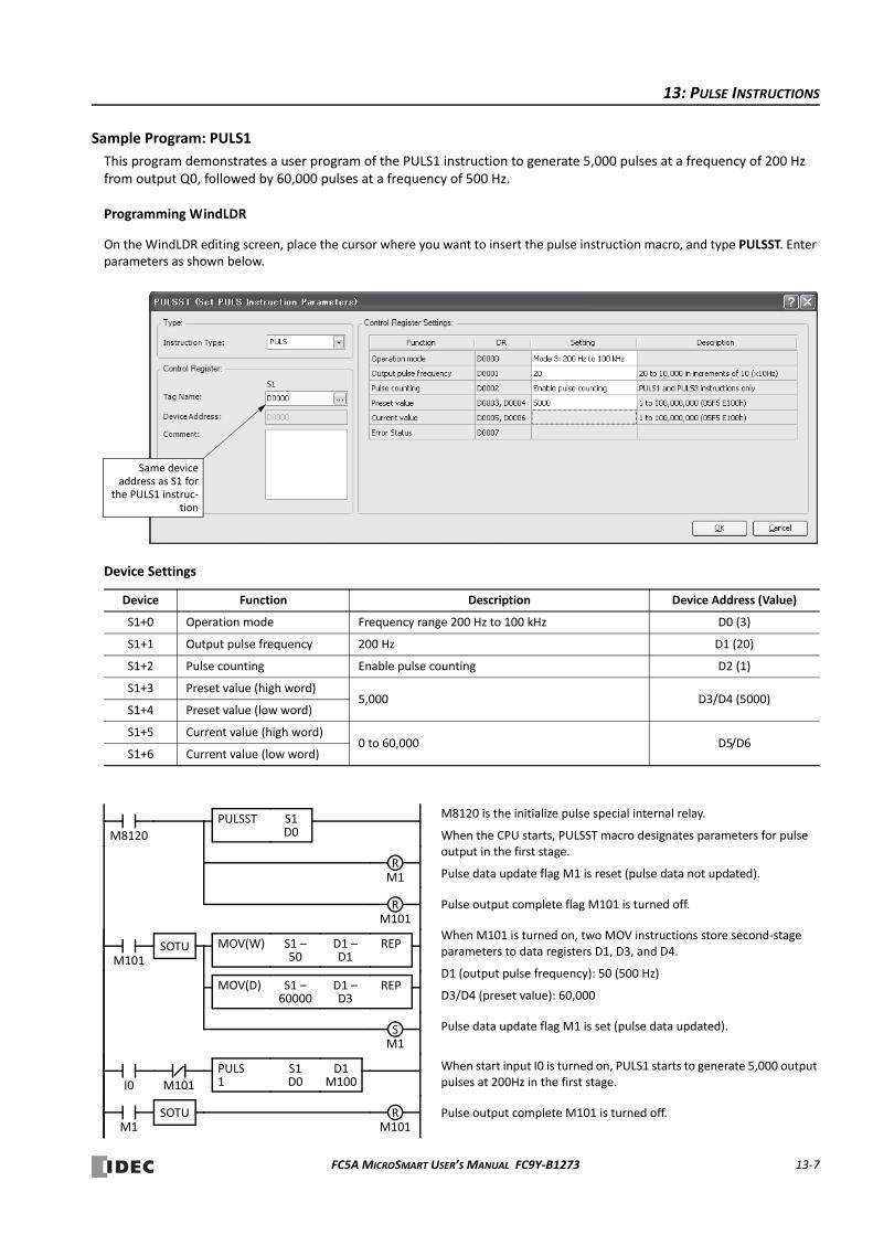
13: PULSE INSTRUCTIONS
Sample Program: PULS1
This program demonstrates a user program of the PULS1 instruction to generate 5,000 pulses at a frequency of 200 Hz from output Q0, followed by 60,000 pulses at a frequency of 500 Hz.
Programming WindLDR
On the WindLDR editing screen, place the cursor where you want to insert the pulse instruction macro, and type PULSST. Enter parameters as shown below.
Device Settings
Device Function Description Device Address (Value)
S1+0 Operation mode Frequency range 200 Hz to 100 kHz D0 (3)
S1+1 Output pulse frequency 200 Hz D1 (20)
S1+2 Pulse counting Enable pulse counting D2 (1)
S1+3 Preset value (high word)5,000 D3/D4 (5000)
S1+4 Preset value (low word)
S1+5 Current value (high word)0 to 60,000 D5/D6
S1+6 Current value (low word)
Same deviceaddress as S1 for
the PULS1 instruc‐tion
M8120
REPS1 –50
MOV(W) D1 –D1M101
SOTU
M8120 is the initialize pulse special internal relay.
When the CPU starts, PULSST macro designates parameters for pulse output in the first stage.
Pulse data update flag M1 is reset (pulse data not updated).
Pulse output complete flag M101 is turned off.
When M101 is turned on, two MOV instructions store second‐stage parameters to data registers D1, D3, and D4.
D1 (output pulse frequency): 50 (500 Hz)
D3/D4 (preset value): 60,000
Pulse data update flag M1 is set (pulse data updated).
When start input I0 is turned on, PULS1 starts to generate 5,000 output pulses at 200Hz in the first stage.
Pulse output complete M101 is turned off.
I0
SOTUM1
S1D0
PULSST
M1S
M1R
M101R
REPS1 –60000
MOV(D) D1 –D3
M101R
M101
D1M100
PULS1
S1D0
FC5A MICROSMART USER’S MANUAL FC9Y‐B1273 13‐7
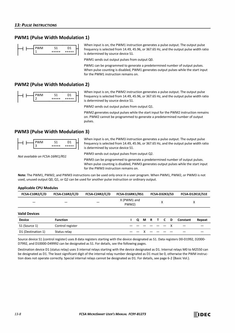
13: PULSE INSTRUCTIONS
PWM1 (Pulse Width Modulation 1)
PWM2 (Pulse Width Modulation 2)
PWM3 (Pulse Width Modulation 3)
Note: The PWM1, PWM2, and PWM3 instructions can be used only once in a user program. When PWM1, PWM2, or PWM3 is not used, unused output Q0, Q1, or Q2 can be used for another pulse instruction or ordinary output.
Applicable CPU Modules
Valid Devices
Source device S1 (control register) uses 8 data registers starting with the device designated as S1. Data registers D0‐D1992, D2000‐D7992, and D10000‐D49992 can be designated as S1. For details, see the following pages.
Destination device D1 (status relay) uses 3 internal relays starting with the device designated as D1. Internal relays M0 to M2550 can be designated as D1. The least significant digit of the internal relay number designated as D1 must be 0, otherwise the PWM instruc‐tion does not operate correctly. Special internal relays cannot be designated as D1. For details, see page 6‐2 (Basic Vol.).
FC5A‐C10R2/C/D FC5A‐C16R2/C/D FC5A‐C24R2/C/D FC5A‐D16RK1/RS1 FC5A‐D32K3/S3 FC5A‐D12K1E/S1E
— — —X (PWM1 and
PWM2)X X
Device Function I Q M R T C D Constant Repeat
S1 (Source 1) Control register — — — — — — X — —
D1 (Destination 1) Status relay — — X — — — — — —
When input is on, the PWM1 instruction generates a pulse output. The output pulse frequency is selected from 14.49, 45.96, or 367.65 Hz, and the output pulse width ratio is determined by source device S1.
PWM1 sends out output pulses from output Q0.
PWM1 can be programmed to generate a predetermined number of output pulses. When pulse counting is disabled, PWM1 generates output pulses while the start input for the PWM1 instruction remains on.
PWM1
S1*****
D1*****
When input is on, the PWM2 instruction generates a pulse output. The output pulse frequency is selected from 14.49, 45.96, or 367.65 Hz, and the output pulse width ratio is determined by source device S1.
PWM2 sends out output pulses from output Q1.
PWM2 generates output pulses while the start input for the PWM2 instruction remains on. PWM2 cannot be programmed to generate a predetermined number of output pulses.
PWM2
S1*****
D1*****
When input is on, the PWM3 instruction generates a pulse output. The output pulse frequency is selected from 14.49, 45.96, or 367.65 Hz, and the output pulse width ratio is determined by source device S1.
PWM3 sends out output pulses from output Q2.
PWM3 can be programmed to generate a predetermined number of output pulses. When pulse counting is disabled, PWM3 generates output pulses while the start input for the PWM3 instruction remains on.
PWM3
S1*****
D1*****
Not available on FC5A‐16RK1/RS1
13‐8 FC5A MICROSMART USER’S MANUAL FC9Y‐B1273

13: PULSE INSTRUCTIONS
Source Device S1 (Control Register)
Store appropriate values to data registers starting with the device designated by S1 before executing the PWM instruc‐tion as required, and make sure that the values are within the valid range. Devices S1+5 through S1+7 are for read only.
Note: Devices for high and low words can be swapped on upgraded CPU modules with system program version 110 or higher. See page 5‐46 (Basic Vol.).
S1+0 Output Pulse Frequency
The value stored in the data register designated by device S1+0 determines the pulse output frequency.
S1+1 Pulse Width Ratio
The value stored in the data register designated by device S1+1 specifies the pulse width ratio of the pulse output in per‐cent of the period determined by the output pulse frequency selected with S1+0. Valid values for device S1+1 are 1 through 100.
S1+2 Pulse Counting
Pulse counting can be enabled for the PWM1 and PWM3 instructions only. With pulse counting enabled, PWM1 or PWM3 generates a predetermined number of output pulses as designated by devices S1+3 and S1+4. With pulse count‐ing disabled, the PWM instruction generates output pulses while the start input for the PWM instruction remains on.
0: Disable pulse counting
1: Enable pulse counting (PWM1/PWM3 only)
When programming PWM2, store 0 to the data register designated by S1+2.
Device Function Description R/W
S1+0 Output pulse frequency
FC5A‐D16RK1/RS1, FC5A‐D32K3/S30: 11.44 Hz1: 45.78 Hz2: 366.2 HzFC5A‐D12K1E/S1E0: 15.26 Hz1: 61.04 Hz2: 488.3 Hz
R/W
S1+1 Pulse width ratio1 to 100 (1% to 100% of the period determined by output pulse frequency S1+0)
R/W
S1+2 Pulse counting0: Disable pulse counting1: Enable pulse counting (PWM1/PWM3 only)
R/W
S1+3 Preset value (high word)1 to 100,000,000 (05F5 E100h) (PWM1/PWM3 only) R/W
S1+4 Preset value (low word)
S1+5 Current value (high word)1 to 100,000,000 (05F5 E100h) (PWM1/PWM3 only) R
S1+6 Current value (low word)
S1+7 Error status 0 to 5 R
FC5A‐D16RK1/RS1, FC5A‐D32K3/S3
0: 11.44 Hz
1: 45.78 Hz
2: 366.2 Hz
FC5A‐D12K1E/S1E
0: 15.26 Hz
1: 61.04 Hz
2: 488.3 Hz
Pulse Width = Period Pulse Width Ratio (%)
Pulse Width PeriodPulse Width Ratio
100-------------------------------------------=
1Output Pulse Frequency---------------------------------------------------------- Pulse Width Ratio
100-------------------------------------------=
Period (69.01, 21.76, or 2.72 ms)
FC5A MICROSMART USER’S MANUAL FC9Y‐B1273 13‐9
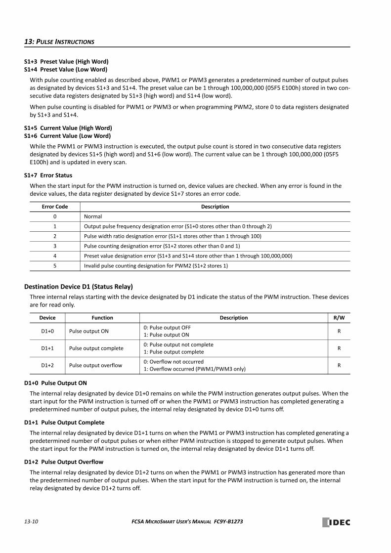
13: PULSE INSTRUCTIONS
S1+3 Preset Value (High Word)S1+4 Preset Value (Low Word)
With pulse counting enabled as described above, PWM1 or PWM3 generates a predetermined number of output pulses as designated by devices S1+3 and S1+4. The preset value can be 1 through 100,000,000 (05F5 E100h) stored in two con‐secutive data registers designated by S1+3 (high word) and S1+4 (low word).
When pulse counting is disabled for PWM1 or PWM3 or when programming PWM2, store 0 to data registers designated by S1+3 and S1+4.
S1+5 Current Value (High Word)S1+6 Current Value (Low Word)
While the PWM1 or PWM3 instruction is executed, the output pulse count is stored in two consecutive data registers designated by devices S1+5 (high word) and S1+6 (low word). The current value can be 1 through 100,000,000 (05F5 E100h) and is updated in every scan.
S1+7 Error Status
When the start input for the PWM instruction is turned on, device values are checked. When any error is found in the device values, the data register designated by device S1+7 stores an error code.
Destination Device D1 (Status Relay)
Three internal relays starting with the device designated by D1 indicate the status of the PWM instruction. These devices are for read only.
D1+0 Pulse Output ON
The internal relay designated by device D1+0 remains on while the PWM instruction generates output pulses. When the start input for the PWM instruction is turned off or when the PWM1 or PWM3 instruction has completed generating a predetermined number of output pulses, the internal relay designated by device D1+0 turns off.
D1+1 Pulse Output Complete
The internal relay designated by device D1+1 turns on when the PWM1 or PWM3 instruction has completed generating a predetermined number of output pulses or when either PWM instruction is stopped to generate output pulses. When the start input for the PWM instruction is turned on, the internal relay designated by device D1+1 turns off.
D1+2 Pulse Output Overflow
The internal relay designated by device D1+2 turns on when the PWM1 or PWM3 instruction has generated more than the predetermined number of output pulses. When the start input for the PWM instruction is turned on, the internal relay designated by device D1+2 turns off.
Error Code Description
0 Normal
1 Output pulse frequency designation error (S1+0 stores other than 0 through 2)
2 Pulse width ratio designation error (S1+1 stores other than 1 through 100)
3 Pulse counting designation error (S1+2 stores other than 0 and 1)
4 Preset value designation error (S1+3 and S1+4 store other than 1 through 100,000,000)
5 Invalid pulse counting designation for PWM2 (S1+2 stores 1)
Device Function Description R/W
D1+0 Pulse output ON0: Pulse output OFF1: Pulse output ON
R
D1+1 Pulse output complete0: Pulse output not complete1: Pulse output complete
R
D1+2 Pulse output overflow0: Overflow not occurred1: Overflow occurred (PWM1/PWM3 only)
R
13‐10 FC5A MICROSMART USER’S MANUAL FC9Y‐B1273
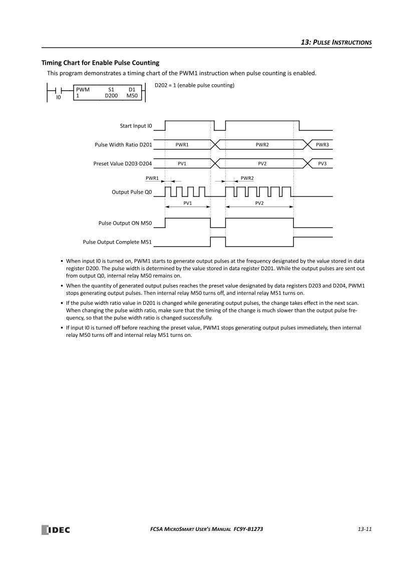
13: PULSE INSTRUCTIONS
Timing Chart for Enable Pulse Counting
This program demonstrates a timing chart of the PWM1 instruction when pulse counting is enabled.
D1M50I0
PWM1
S1D200
D202 = 1 (enable pulse counting)
• When input I0 is turned on, PWM1 starts to generate output pulses at the frequency designated by the value stored in data register D200. The pulse width is determined by the value stored in data register D201. While the output pulses are sent out from output Q0, internal relay M50 remains on.
• When the quantity of generated output pulses reaches the preset value designated by data registers D203 and D204, PWM1 stops generating output pulses. Then internal relay M50 turns off, and internal relay M51 turns on.
• If the pulse width ratio value in D201 is changed while generating output pulses, the change takes effect in the next scan. When changing the pulse width ratio, make sure that the timing of the change is much slower than the output pulse fre‐quency, so that the pulse width ratio is changed successfully.
• If input I0 is turned off before reaching the preset value, PWM1 stops generating output pulses immediately, then internal relay M50 turns off and internal relay M51 turns on.
Output Pulse Q0
Pulse Width Ratio D201
PV1
PWR1
Start Input I0
PWR2 PWR3
Preset Value D203∙D204 PV1 PV2 PV3
Pulse Output ON M50
Pulse Output Complete M51
PV2
PWR1 PWR2
FC5A MICROSMART USER’S MANUAL FC9Y‐B1273 13‐11
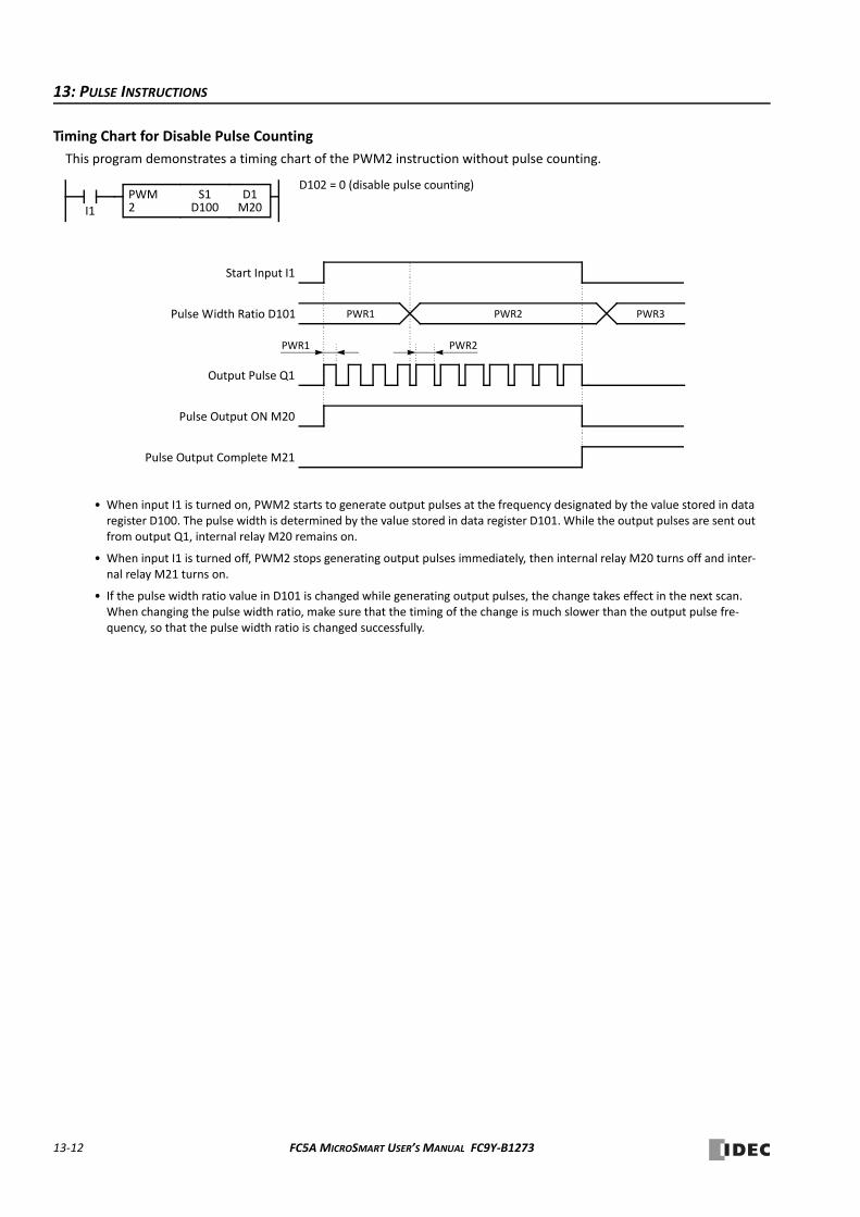
13: PULSE INSTRUCTIONS
Timing Chart for Disable Pulse Counting
This program demonstrates a timing chart of the PWM2 instruction without pulse counting.
D1M20I1
PWM2
S1D100
D102 = 0 (disable pulse counting)
Output Pulse Q1
Pulse Width Ratio D101 PWR1
Start Input I1
• When input I1 is turned on, PWM2 starts to generate output pulses at the frequency designated by the value stored in data register D100. The pulse width is determined by the value stored in data register D101. While the output pulses are sent out from output Q1, internal relay M20 remains on.
• When input I1 is turned off, PWM2 stops generating output pulses immediately, then internal relay M20 turns off and inter‐nal relay M21 turns on.
• If the pulse width ratio value in D101 is changed while generating output pulses, the change takes effect in the next scan. When changing the pulse width ratio, make sure that the timing of the change is much slower than the output pulse fre‐quency, so that the pulse width ratio is changed successfully.
PWR2 PWR3
Pulse Output ON M20
Pulse Output Complete M21
PWR1 PWR2
13‐12 FC5A MICROSMART USER’S MANUAL FC9Y‐B1273
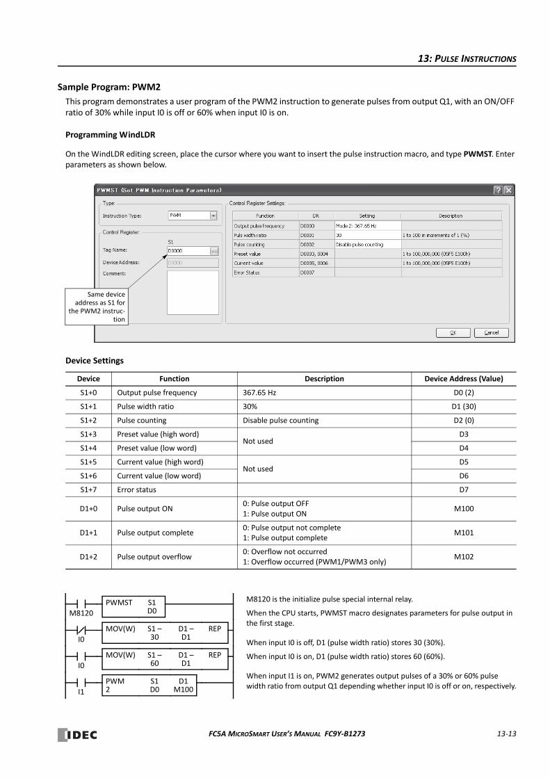
13: PULSE INSTRUCTIONS
Sample Program: PWM2
This program demonstrates a user program of the PWM2 instruction to generate pulses from output Q1, with an ON/OFF ratio of 30% while input I0 is off or 60% when input I0 is on.
Programming WindLDR
On the WindLDR editing screen, place the cursor where you want to insert the pulse instruction macro, and type PWMST. Enter parameters as shown below.
Device Settings
Device Function Description Device Address (Value)
S1+0 Output pulse frequency 367.65 Hz D0 (2)
S1+1 Pulse width ratio 30% D1 (30)
S1+2 Pulse counting Disable pulse counting D2 (0)
S1+3 Preset value (high word)Not used
D3
S1+4 Preset value (low word) D4
S1+5 Current value (high word)Not used
D5
S1+6 Current value (low word) D6
S1+7 Error status D7
D1+0 Pulse output ON0: Pulse output OFF1: Pulse output ON
M100
D1+1 Pulse output complete0: Pulse output not complete1: Pulse output complete
M101
D1+2 Pulse output overflow0: Overflow not occurred1: Overflow occurred (PWM1/PWM3 only)
M102
Same deviceaddress as S1 for
the PWM2 instruc‐tion
M8120
I0
M8120 is the initialize pulse special internal relay.
When the CPU starts, PWMST macro designates parameters for pulse output in the first stage.
When input I0 is off, D1 (pulse width ratio) stores 30 (30%).
When input I0 is on, D1 (pulse width ratio) stores 60 (60%).
When input I1 is on, PWM2 generates output pulses of a 30% or 60% pulse width ratio from output Q1 depending whether input I0 is off or on, respectively.
REPS1 –30
MOV(W) D1 –D1
REPS1 –60
MOV(W) D1 –D1
I0
D1M100
PWM2
S1D0I1
S1D0
PWMST
FC5A MICROSMART USER’S MANUAL FC9Y‐B1273 13‐13
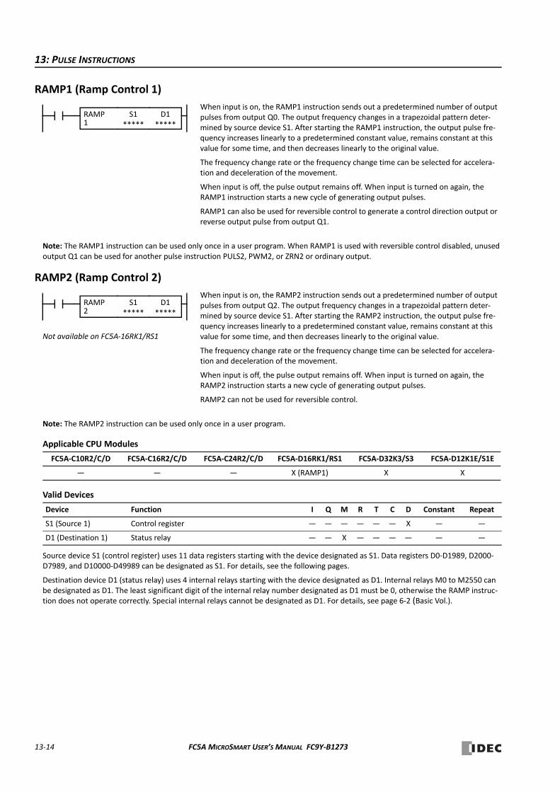
13: PULSE INSTRUCTIONS
RAMP1 (Ramp Control 1)
Note: The RAMP1 instruction can be used only once in a user program. When RAMP1 is used with reversible control disabled, unused output Q1 can be used for another pulse instruction PULS2, PWM2, or ZRN2 or ordinary output.
RAMP2 (Ramp Control 2)
Note: The RAMP2 instruction can be used only once in a user program.
Applicable CPU Modules
Valid Devices
Source device S1 (control register) uses 11 data registers starting with the device designated as S1. Data registers D0‐D1989, D2000‐D7989, and D10000‐D49989 can be designated as S1. For details, see the following pages.
Destination device D1 (status relay) uses 4 internal relays starting with the device designated as D1. Internal relays M0 to M2550 can be designated as D1. The least significant digit of the internal relay number designated as D1 must be 0, otherwise the RAMP instruc‐tion does not operate correctly. Special internal relays cannot be designated as D1. For details, see page 6‐2 (Basic Vol.).
FC5A‐C10R2/C/D FC5A‐C16R2/C/D FC5A‐C24R2/C/D FC5A‐D16RK1/RS1 FC5A‐D32K3/S3 FC5A‐D12K1E/S1E
— — — X (RAMP1) X X
Device Function I Q M R T C D Constant Repeat
S1 (Source 1) Control register — — — — — — X — —
D1 (Destination 1) Status relay — — X — — — — — —
When input is on, the RAMP1 instruction sends out a predetermined number of output pulses from output Q0. The output frequency changes in a trapezoidal pattern deter‐mined by source device S1. After starting the RAMP1 instruction, the output pulse fre‐quency increases linearly to a predetermined constant value, remains constant at this value for some time, and then decreases linearly to the original value.
The frequency change rate or the frequency change time can be selected for accelera‐tion and deceleration of the movement.
When input is off, the pulse output remains off. When input is turned on again, the RAMP1 instruction starts a new cycle of generating output pulses.
RAMP1 can also be used for reversible control to generate a control direction output or reverse output pulse from output Q1.
S1*****
D1*****
RAMP1
When input is on, the RAMP2 instruction sends out a predetermined number of output pulses from output Q2. The output frequency changes in a trapezoidal pattern deter‐mined by source device S1. After starting the RAMP2 instruction, the output pulse fre‐quency increases linearly to a predetermined constant value, remains constant at this value for some time, and then decreases linearly to the original value.
The frequency change rate or the frequency change time can be selected for accelera‐tion and deceleration of the movement.
When input is off, the pulse output remains off. When input is turned on again, the RAMP2 instruction starts a new cycle of generating output pulses.
RAMP2 can not be used for reversible control.
S1*****
D1*****
Not available on FC5A‐16RK1/RS1
RAMP2
13‐14 FC5A MICROSMART USER’S MANUAL FC9Y‐B1273
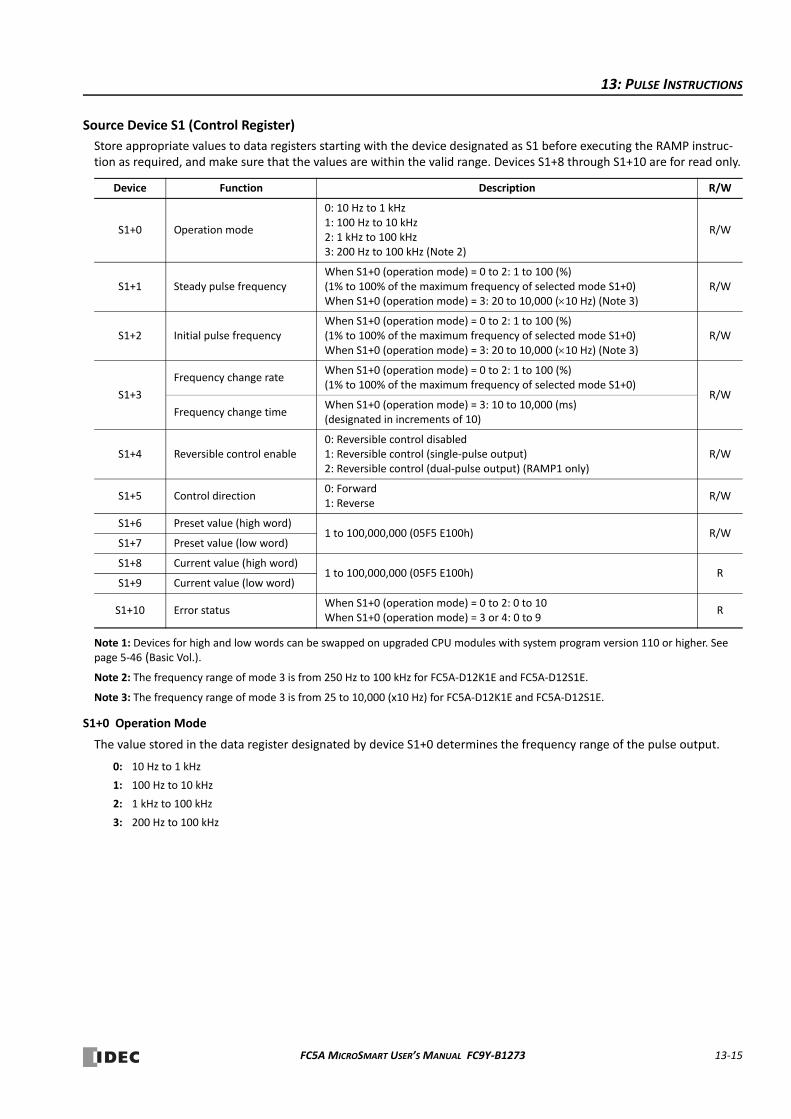
13: PULSE INSTRUCTIONS
Source Device S1 (Control Register)
Store appropriate values to data registers starting with the device designated as S1 before executing the RAMP instruc‐tion as required, and make sure that the values are within the valid range. Devices S1+8 through S1+10 are for read only.
Note 1: Devices for high and low words can be swapped on upgraded CPU modules with system program version 110 or higher. See page 5‐46 (Basic Vol.).
Note 2: The frequency range of mode 3 is from 250 Hz to 100 kHz for FC5A‐D12K1E and FC5A‐D12S1E.
Note 3: The frequency range of mode 3 is from 25 to 10,000 (x10 Hz) for FC5A‐D12K1E and FC5A‐D12S1E.
S1+0 Operation Mode
The value stored in the data register designated by device S1+0 determines the frequency range of the pulse output.
0: 10 Hz to 1 kHz
1: 100 Hz to 10 kHz
2: 1 kHz to 100 kHz
3: 200 Hz to 100 kHz
Device Function Description R/W
S1+0 Operation mode
0: 10 Hz to 1 kHz1: 100 Hz to 10 kHz2: 1 kHz to 100 kHz3: 200 Hz to 100 kHz (Note 2)
R/W
S1+1 Steady pulse frequencyWhen S1+0 (operation mode) = 0 to 2: 1 to 100 (%)(1% to 100% of the maximum frequency of selected mode S1+0)When S1+0 (operation mode) = 3: 20 to 10,000 (10 Hz) (Note 3)
R/W
S1+2 Initial pulse frequencyWhen S1+0 (operation mode) = 0 to 2: 1 to 100 (%)(1% to 100% of the maximum frequency of selected mode S1+0)When S1+0 (operation mode) = 3: 20 to 10,000 (10 Hz) (Note 3)
R/W
S1+3
Frequency change rateWhen S1+0 (operation mode) = 0 to 2: 1 to 100 (%)(1% to 100% of the maximum frequency of selected mode S1+0)
R/W
Frequency change timeWhen S1+0 (operation mode) = 3: 10 to 10,000 (ms)(designated in increments of 10)
S1+4 Reversible control enable0: Reversible control disabled1: Reversible control (single‐pulse output)2: Reversible control (dual‐pulse output) (RAMP1 only)
R/W
S1+5 Control direction0: Forward1: Reverse
R/W
S1+6 Preset value (high word)1 to 100,000,000 (05F5 E100h) R/W
S1+7 Preset value (low word)
S1+8 Current value (high word)1 to 100,000,000 (05F5 E100h) R
S1+9 Current value (low word)
S1+10 Error statusWhen S1+0 (operation mode) = 0 to 2: 0 to 10When S1+0 (operation mode) = 3 or 4: 0 to 9
R
FC5A MICROSMART USER’S MANUAL FC9Y‐B1273 13‐15

13: PULSE INSTRUCTIONS
S1+1 Steady Pulse Frequency
When S1+0 is set to 0 through 2, the value stored in the data register designated by device S1+1 specifies the frequency of the steady pulse output in percent of the maximum of the frequency range selected by S1+0. Valid values for device S1+1 are 1 through 100, thus the output pulse frequency can be 10 Hz to 1 kHz (operation mode 0), 100 Hz to 10 kHz (operation mode 1), or 1 kHz to 100 kHz (operation mode 2).
When S1+0 is set to 3 (200 Hz to 100 kHz), valid values for device S1+1 are 20 through 10,000 (in increments of 10) and the S1+1 value multiplied by 10 determines the steady pulse frequency, thus the output pulse frequency can be set in increments of 10 Hz. The output frequency error is ±5% maximum.
S1+2 Initial Pulse Frequency
When S1+0 is set to 0 through 2, the value stored in the data register designated by device S1+2 specifies the frequency of the initial pulse output in percent of the maximum of the frequency range selected by S1+0. Valid values for device S1+2 are 1 through 100, thus the initial pulse frequency can be 10 Hz to 1 kHz (operation mode 0), 100 Hz to 10 kHz (operation mode 1), or 1 kHz to 100 kHz (operation mode 2).
When S1+0 is set to 3 (200 Hz to 100 kHz), valid values for device S1+2 are 20 through 10,000 (in increments of 10) and the S1+2 value multiplied by 10 determines the initial pulse frequency, thus the initial pulse frequency can be set in incre‐ments of 10 Hz. The output frequency error is ±5% maximum.
S1+3 Frequency Change Rate / Frequency Change Time
When S1+0 is set to 0 through 2, the value stored in the data register designated by device S1+3 determines the rate of pulse output frequency change for a period of 10 ms in percent of the maximum of the frequency range selected by S1+0. Valid values for device S1+3 are 1 through 100, thus the frequency change rate can be 10 Hz to 1 kHz (operation mode 0), 100 Hz to 10 kHz (operation mode 1), or 1 kHz to 100 kHz (operation mode 2).
When S1+0 is set to 3, the value stored in the data register designated by device S1+3 determines the frequency change time. Valid values are 10 through 10,000 in increments of 10, thus the frequency change time can be 10 to 10,000 ms. The value at the lowest digit is omitted.
The same frequency change rate and frequency change time apply to the accelerating and decelerating periods of the trapezoidal frequency change pattern.
Operation Mode (S1+0) S1+1 Steady Pulse Frequency (Hz)
0 to 2 1 to 100 Maximum frequency selected by S1+0 S1+1 value (%)
3 20 to 10,000 S1+1 value 10
Operation Mode (S1+0) S1+2 Initial Pulse Frequency (Hz)
0 to 2 1 to 100 Maximum frequency selected by S1+0 S1+2 value (%)
3 20 to 10,000 S1+2 value 10
Operation Mode
Frequency Change Rate / Frequency Change Time
0 to 2 Frequency change rate in 10 ms (Hz) Maximum frequency (Hz) selected by S1+0 S1+3 value (%)
3 Frequency change time (ms) Frequency change time (ms) selected by S1+3
Output Pulse
Initial Pulse Frequency
Steady Pulse Frequency
Modes 0 to 2
10 ms
Frequency Change Rate
Mode 3
Frequency Change Time
13‐16 FC5A MICROSMART USER’S MANUAL FC9Y‐B1273
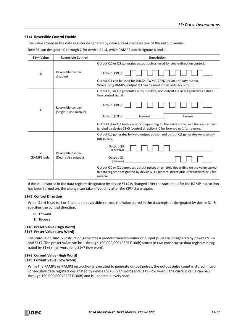
13: PULSE INSTRUCTIONS
S1+4 Reversible Control Enable
The value stored in the data register designated by device S1+4 specifies one of the output modes.
RAMP1 can designate 0 through 2 for device S1+4, while RAMP2 can designate 0 and 1.
If the value stored in the data register designated by device S1+4 is changed after the start input for the RAMP instruction has been turned on, the change can take effect only after the CPU starts again.
S1+5 Control Direction
When S1+4 is set to 1 or 2 to enable reversible control, the value stored in the data register designated by device S1+5 specifies the control direction.
0: Forward
1: Reverse
S1+6 Preset Value (High Word)S1+7 Preset Value (Low Word)
The RAMP1 or RAMP2 instruction generates a predetermined number of output pulses as designated by devices S1+6 and S1+7. The preset value can be 1 through 100,000,000 (05F5 E100h) stored in two consecutive data registers desig‐nated by S1+6 (high word) and S1+7 (low word).
S1+8 Current Value (High Word)S1+9 Current Value (Low Word)
While the RAMP1 or RAMP2 instruction is executed to generate output pulses, the output pulse count is stored in two consecutive data registers designated by devices S1+8 (high word) and S1+9 (low word). The current value can be 1 through 100,000,000 (05F5 E100h) and is updated in every scan.
S1+4 Value Reversible Control Description
0Reversible control disabled
Output Q0 or Q2 generates output pulses; used for single‐direction control.
Output Q1 can be used for PULS2, PWM2, ZRN2, or an ordinary output.When using RAMP2, output Q3 can be used for an ordinary output.
1Reversible control(Single‐pulse output)
Output Q0 or Q2 generates output pulses, and output Q1 or Q3 generates a direc‐tion control signal.
Output Q1 or Q3 turns on or off depending on the value stored in data register des‐ignated by device S1+5 (control direction): 0 for forward or 1 for reverse.
2(RAMP1 only)
Reversible control(Dual‐pulse output)
Output Q0 generates forward output pulses, and output Q1 generates reverse out‐put pulses.
Output Q0 or Q1 generates output pulses alternately depending on the value stored in data register designated by device S1+5 (control direction): 0 for forward or 1 for reverse.
Output Q0/Q2
Output Q0/Q2
Output Q1/Q3 Forward Reverse
Output Q0
Output Q1
(Forward)
(Reverse)
FC5A MICROSMART USER’S MANUAL FC9Y‐B1273 13‐17
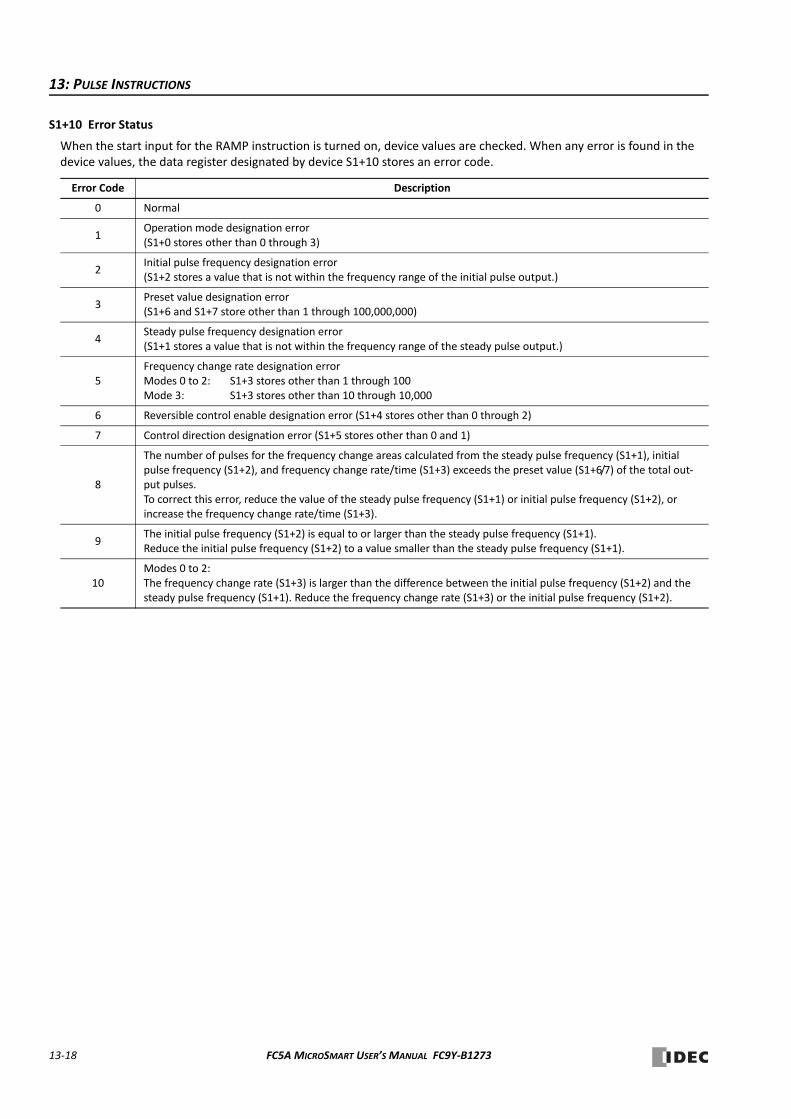
13: PULSE INSTRUCTIONS
S1+10 Error Status
When the start input for the RAMP instruction is turned on, device values are checked. When any error is found in the device values, the data register designated by device S1+10 stores an error code.
Error Code Description
0 Normal
1Operation mode designation error (S1+0 stores other than 0 through 3)
2Initial pulse frequency designation error (S1+2 stores a value that is not within the frequency range of the initial pulse output.)
3Preset value designation error (S1+6 and S1+7 store other than 1 through 100,000,000)
4Steady pulse frequency designation error (S1+1 stores a value that is not within the frequency range of the steady pulse output.)
5Frequency change rate designation error Modes 0 to 2: S1+3 stores other than 1 through 100Mode 3: S1+3 stores other than 10 through 10,000
6 Reversible control enable designation error (S1+4 stores other than 0 through 2)
7 Control direction designation error (S1+5 stores other than 0 and 1)
8
The number of pulses for the frequency change areas calculated from the steady pulse frequency (S1+1), initial pulse frequency (S1+2), and frequency change rate/time (S1+3) exceeds the preset value (S1+6/7) of the total out‐put pulses. To correct this error, reduce the value of the steady pulse frequency (S1+1) or initial pulse frequency (S1+2), or increase the frequency change rate/time (S1+3).
9The initial pulse frequency (S1+2) is equal to or larger than the steady pulse frequency (S1+1). Reduce the initial pulse frequency (S1+2) to a value smaller than the steady pulse frequency (S1+1).
10Modes 0 to 2:The frequency change rate (S1+3) is larger than the difference between the initial pulse frequency (S1+2) and the steady pulse frequency (S1+1). Reduce the frequency change rate (S1+3) or the initial pulse frequency (S1+2).
13‐18 FC5A MICROSMART USER’S MANUAL FC9Y‐B1273
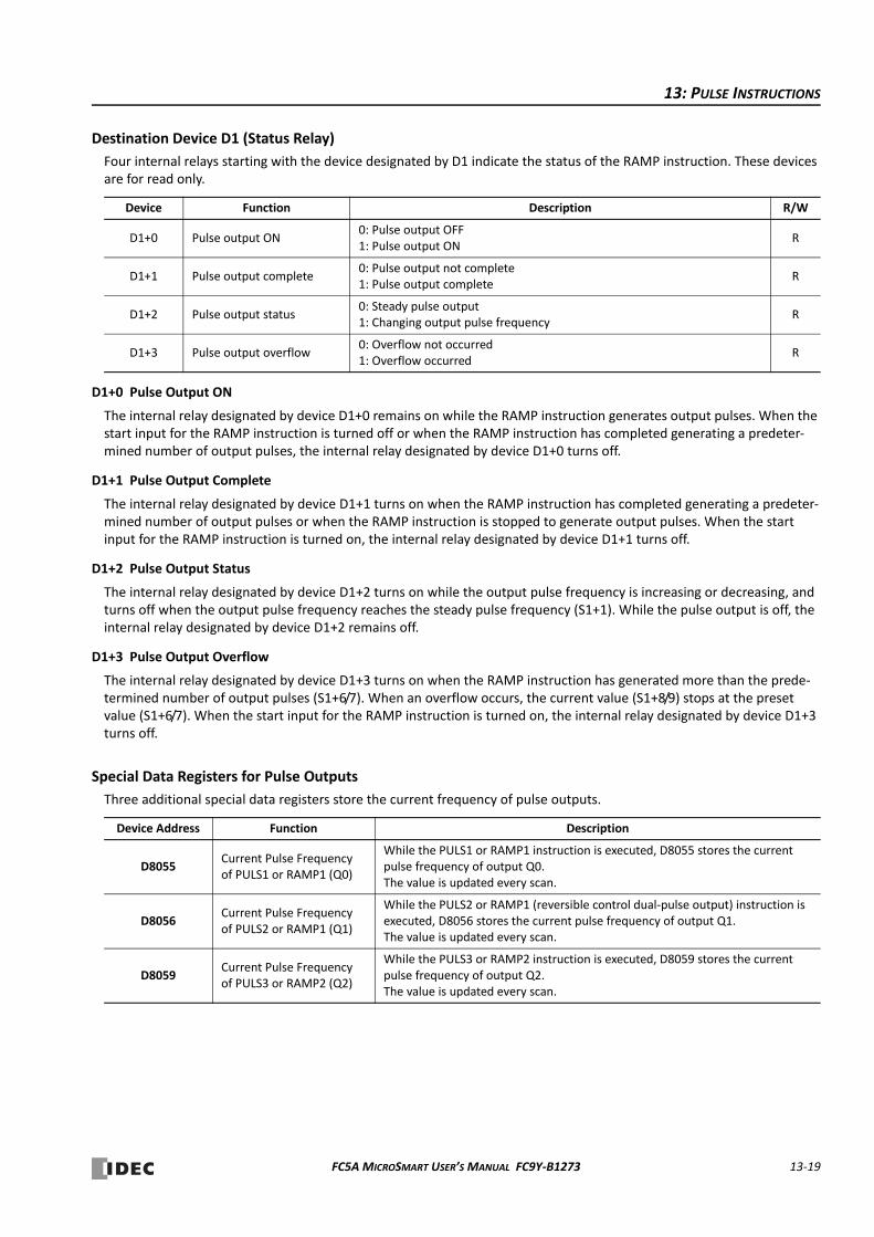
13: PULSE INSTRUCTIONS
Destination Device D1 (Status Relay)
Four internal relays starting with the device designated by D1 indicate the status of the RAMP instruction. These devices are for read only.
D1+0 Pulse Output ON
The internal relay designated by device D1+0 remains on while the RAMP instruction generates output pulses. When the start input for the RAMP instruction is turned off or when the RAMP instruction has completed generating a predeter‐mined number of output pulses, the internal relay designated by device D1+0 turns off.
D1+1 Pulse Output Complete
The internal relay designated by device D1+1 turns on when the RAMP instruction has completed generating a predeter‐mined number of output pulses or when the RAMP instruction is stopped to generate output pulses. When the start input for the RAMP instruction is turned on, the internal relay designated by device D1+1 turns off.
D1+2 Pulse Output Status
The internal relay designated by device D1+2 turns on while the output pulse frequency is increasing or decreasing, and turns off when the output pulse frequency reaches the steady pulse frequency (S1+1). While the pulse output is off, the internal relay designated by device D1+2 remains off.
D1+3 Pulse Output Overflow
The internal relay designated by device D1+3 turns on when the RAMP instruction has generated more than the prede‐termined number of output pulses (S1+6/7). When an overflow occurs, the current value (S1+8/9) stops at the preset value (S1+6/7). When the start input for the RAMP instruction is turned on, the internal relay designated by device D1+3 turns off.
Special Data Registers for Pulse Outputs
Three additional special data registers store the current frequency of pulse outputs.
Device Function Description R/W
D1+0 Pulse output ON0: Pulse output OFF1: Pulse output ON
R
D1+1 Pulse output complete0: Pulse output not complete1: Pulse output complete
R
D1+2 Pulse output status0: Steady pulse output1: Changing output pulse frequency
R
D1+3 Pulse output overflow0: Overflow not occurred1: Overflow occurred
R
Device Address Function Description
D8055Current Pulse Frequency of PULS1 or RAMP1 (Q0)
While the PULS1 or RAMP1 instruction is executed, D8055 stores the current pulse frequency of output Q0. The value is updated every scan.
D8056Current Pulse Frequency of PULS2 or RAMP1 (Q1)
While the PULS2 or RAMP1 (reversible control dual‐pulse output) instruction is executed, D8056 stores the current pulse frequency of output Q1. The value is updated every scan.
D8059Current Pulse Frequency of PULS3 or RAMP2 (Q2)
While the PULS3 or RAMP2 instruction is executed, D8059 stores the current pulse frequency of output Q2. The value is updated every scan.
FC5A MICROSMART USER’S MANUAL FC9Y‐B1273 13‐19
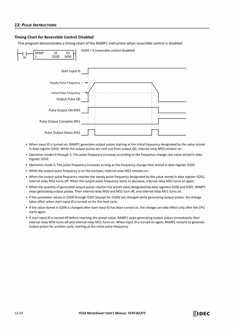
13: PULSE INSTRUCTIONS
Timing Chart for Reversible Control Disabled
This program demonstrates a timing chart of the RAMP1 instruction when reversible control is disabled.
D1M50I0
RAMP1
S1D200
D204 = 0 (reversible control disabled)
• When input I0 is turned on, RAMP1 generates output pulses starting at the initial frequency designated by the value stored in data register D202. While the output pulses are sent out from output Q0, internal relay M50 remains on.
• Operation modes 0 through 2: The pulse frequency increases according to the frequency change rate value stored in data register D203.
• Operation mode 3: The pulse frequency increases as long as the frequency change time stored in data register D203.
• While the output pulse frequency is on the increase, internal relay M52 remains on.
• When the output pulse frequency reaches the steady pulse frequency designated by the value stored in data register D201, internal relay M52 turns off. When the output pulse frequency starts to decrease, internal relay M52 turns on again.
• When the quantity of generated output pulses reaches the preset value designated by data registers D206 and D207, RAMP1 stops generating output pulses. Then internal relay M50 and M52 turn off, and internal relay M51 turns on.
• If the parameter values in D200 through D207 (except for D204) are changed while generating output pulses, the change takes effect when start input I0 is turned on for the next cycle.
• If the value stored in D204 is changed after start input I0 has been turned on, the change can take effect only after the CPU starts again.
• If start input I0 is turned off before reaching the preset value, RAMP1 stops generating output pulses immediately, then internal relay M50 turns off and internal relay M51 turns on. When input I0 is turned on again, RAMP1 restarts to generate output pulses for another cycle, starting at the initial pulse frequency.
Pulse Output Status M52
Output Pulse Q0
Start Input I0
Pulse Output ON M50
Pulse Output Complete M51
Initial Pulse Frequency
Steady Pulse Frequency
13‐20 FC5A MICROSMART USER’S MANUAL FC9Y‐B1273
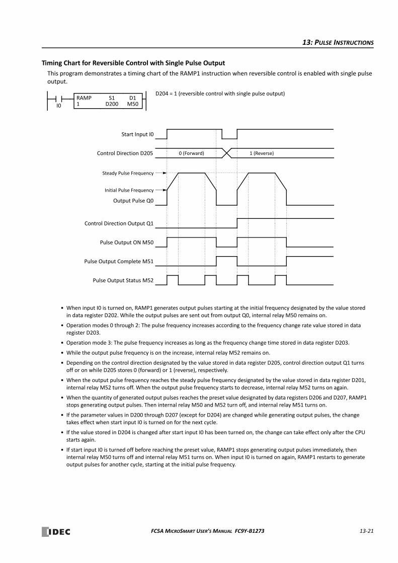
13: PULSE INSTRUCTIONS
Timing Chart for Reversible Control with Single Pulse Output
This program demonstrates a timing chart of the RAMP1 instruction when reversible control is enabled with single pulse output.
D1M50I0
RAMP1
S1D200
D204 = 1 (reversible control with single pulse output)
• When input I0 is turned on, RAMP1 generates output pulses starting at the initial frequency designated by the value stored in data register D202. While the output pulses are sent out from output Q0, internal relay M50 remains on.
• Operation modes 0 through 2: The pulse frequency increases according to the frequency change rate value stored in data register D203.
• Operation mode 3: The pulse frequency increases as long as the frequency change time stored in data register D203.
• While the output pulse frequency is on the increase, internal relay M52 remains on.
• Depending on the control direction designated by the value stored in data register D205, control direction output Q1 turns off or on while D205 stores 0 (forward) or 1 (reverse), respectively.
• When the output pulse frequency reaches the steady pulse frequency designated by the value stored in data register D201, internal relay M52 turns off. When the output pulse frequency starts to decrease, internal relay M52 turns on again.
• When the quantity of generated output pulses reaches the preset value designated by data registers D206 and D207, RAMP1 stops generating output pulses. Then internal relay M50 and M52 turn off, and internal relay M51 turns on.
• If the parameter values in D200 through D207 (except for D204) are changed while generating output pulses, the change takes effect when start input I0 is turned on for the next cycle.
• If the value stored in D204 is changed after start input I0 has been turned on, the change can take effect only after the CPU starts again.
• If start input I0 is turned off before reaching the preset value, RAMP1 stops generating output pulses immediately, then internal relay M50 turns off and internal relay M51 turns on. When input I0 is turned on again, RAMP1 restarts to generate output pulses for another cycle, starting at the initial pulse frequency.
Pulse Output Status M52
Output Pulse Q0
Start Input I0
Control Direction Output Q1
Pulse Output Complete M51
Initial Pulse Frequency
Steady Pulse Frequency
Control Direction D205 0 (Forward) 1 (Reverse)
Pulse Output ON M50
FC5A MICROSMART USER’S MANUAL FC9Y‐B1273 13‐21
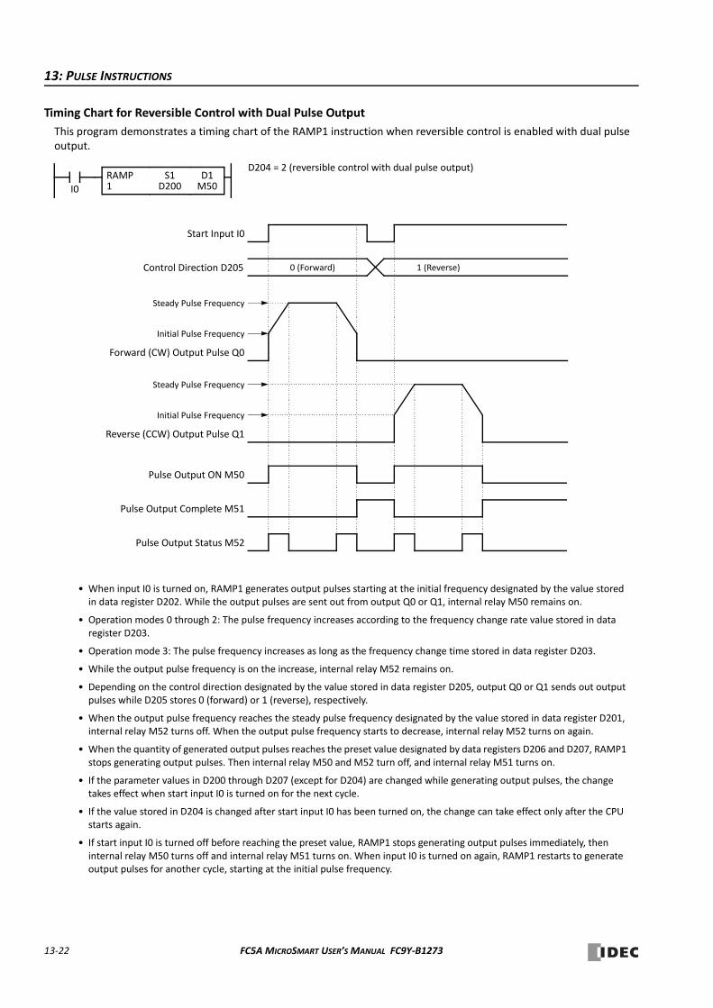
13: PULSE INSTRUCTIONS
Timing Chart for Reversible Control with Dual Pulse Output
This program demonstrates a timing chart of the RAMP1 instruction when reversible control is enabled with dual pulse output.
D1M50I0
RAMP1
S1D200
D204 = 2 (reversible control with dual pulse output)
• When input I0 is turned on, RAMP1 generates output pulses starting at the initial frequency designated by the value stored in data register D202. While the output pulses are sent out from output Q0 or Q1, internal relay M50 remains on.
• Operation modes 0 through 2: The pulse frequency increases according to the frequency change rate value stored in data register D203.
• Operation mode 3: The pulse frequency increases as long as the frequency change time stored in data register D203.
• While the output pulse frequency is on the increase, internal relay M52 remains on.
• Depending on the control direction designated by the value stored in data register D205, output Q0 or Q1 sends out output pulses while D205 stores 0 (forward) or 1 (reverse), respectively.
• When the output pulse frequency reaches the steady pulse frequency designated by the value stored in data register D201, internal relay M52 turns off. When the output pulse frequency starts to decrease, internal relay M52 turns on again.
• When the quantity of generated output pulses reaches the preset value designated by data registers D206 and D207, RAMP1 stops generating output pulses. Then internal relay M50 and M52 turn off, and internal relay M51 turns on.
• If the parameter values in D200 through D207 (except for D204) are changed while generating output pulses, the change takes effect when start input I0 is turned on for the next cycle.
• If the value stored in D204 is changed after start input I0 has been turned on, the change can take effect only after the CPU starts again.
• If start input I0 is turned off before reaching the preset value, RAMP1 stops generating output pulses immediately, then internal relay M50 turns off and internal relay M51 turns on. When input I0 is turned on again, RAMP1 restarts to generate output pulses for another cycle, starting at the initial pulse frequency.
Forward (CW) Output Pulse Q0
Start Input I0
Initial Pulse Frequency
Steady Pulse Frequency
Control Direction D205 0 (Forward) 1 (Reverse)
Pulse Output Status M52
Pulse Output Complete M51
Pulse Output ON M50
Reverse (CCW) Output Pulse Q1
Initial Pulse Frequency
Steady Pulse Frequency
13‐22 FC5A MICROSMART USER’S MANUAL FC9Y‐B1273
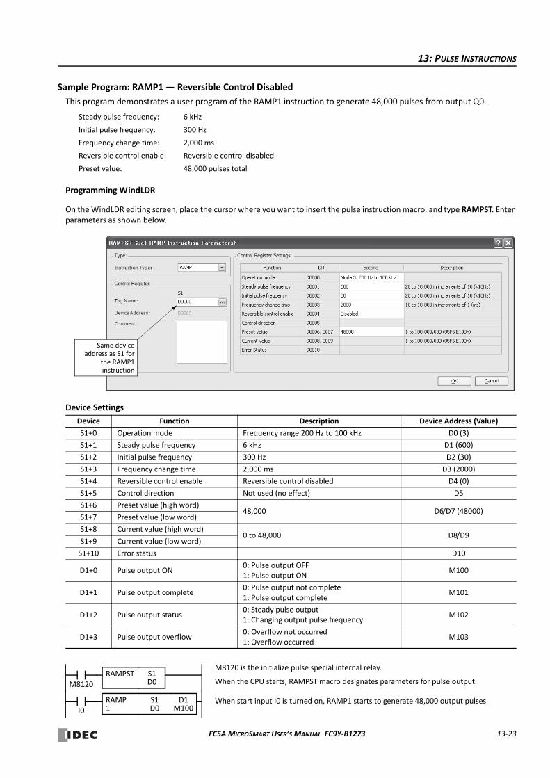
13: PULSE INSTRUCTIONS
Sample Program: RAMP1 — Reversible Control Disabled
This program demonstrates a user program of the RAMP1 instruction to generate 48,000 pulses from output Q0.
Steady pulse frequency: 6 kHz
Initial pulse frequency: 300 Hz
Frequency change time: 2,000 ms
Reversible control enable: Reversible control disabled
Preset value: 48,000 pulses total
Programming WindLDR
On the WindLDR editing screen, place the cursor where you want to insert the pulse instruction macro, and type RAMPST. Enter parameters as shown below.
Device Settings
Device Function Description Device Address (Value)
S1+0 Operation mode Frequency range 200 Hz to 100 kHz D0 (3)
S1+1 Steady pulse frequency 6 kHz D1 (600)
S1+2 Initial pulse frequency 300 Hz D2 (30)
S1+3 Frequency change time 2,000 ms D3 (2000)
S1+4 Reversible control enable Reversible control disabled D4 (0)
S1+5 Control direction Not used (no effect) D5
S1+6 Preset value (high word)48,000 D6/D7 (48000)
S1+7 Preset value (low word)
S1+8 Current value (high word)0 to 48,000 D8/D9
S1+9 Current value (low word)
S1+10 Error status D10
D1+0 Pulse output ON0: Pulse output OFF1: Pulse output ON
M100
D1+1 Pulse output complete0: Pulse output not complete1: Pulse output complete
M101
D1+2 Pulse output status0: Steady pulse output1: Changing output pulse frequency
M102
D1+3 Pulse output overflow0: Overflow not occurred1: Overflow occurred
M103
Same deviceaddress as S1 for
the RAMP1instruction
M8120
M8120 is the initialize pulse special internal relay.
When the CPU starts, RAMPST macro designates parameters for pulse output.
When start input I0 is turned on, RAMP1 starts to generate 48,000 output pulses.I0
D1M100
RAMP1
S1D0
S1D0
RAMPST
FC5A MICROSMART USER’S MANUAL FC9Y‐B1273 13‐23
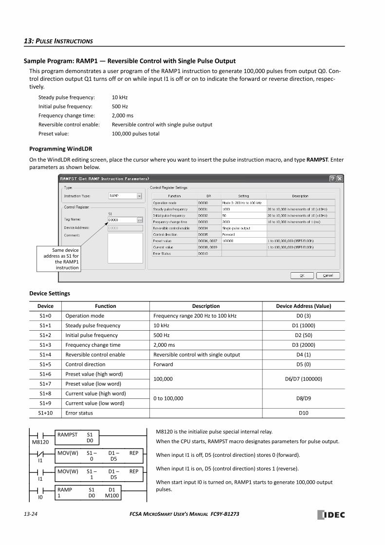
13: PULSE INSTRUCTIONS
Sample Program: RAMP1 — Reversible Control with Single Pulse Output
This program demonstrates a user program of the RAMP1 instruction to generate 100,000 pulses from output Q0. Con‐trol direction output Q1 turns off or on while input I1 is off or on to indicate the forward or reverse direction, respec‐tively.
Steady pulse frequency: 10 kHz
Initial pulse frequency: 500 Hz
Frequency change time: 2,000 ms
Reversible control enable: Reversible control with single pulse output
Preset value: 100,000 pulses total
Programming WindLDR
On the WindLDR editing screen, place the cursor where you want to insert the pulse instruction macro, and type RAMPST. Enter parameters as shown below.
Device Settings
Device Function Description Device Address (Value)
S1+0 Operation mode Frequency range 200 Hz to 100 kHz D0 (3)
S1+1 Steady pulse frequency 10 kHz D1 (1000)
S1+2 Initial pulse frequency 500 Hz D2 (50)
S1+3 Frequency change time 2,000 ms D3 (2000)
S1+4 Reversible control enable Reversible control with single output D4 (1)
S1+5 Control direction Forward D5 (0)
S1+6 Preset value (high word)100,000 D6/D7 (100000)
S1+7 Preset value (low word)
S1+8 Current value (high word)0 to 100,000 D8/D9
S1+9 Current value (low word)
S1+10 Error status D10
Same deviceaddress as S1 for
the RAMP1instruction
M8120
M8120 is the initialize pulse special internal relay.
When the CPU starts, RAMPST macro designates parameters for pulse output.
When input I1 is off, D5 (control direction) stores 0 (forward).
When input I1 is on, D5 (control direction) stores 1 (reverse).
When start input I0 is turned on, RAMP1 starts to generate 100,000 output pulses.
I0
D1M100
RAMP1
S1D0
REPS1 –0
MOV(W) D1 –D5
REPS1 –1
MOV(W) D1 –D5I1
I1
S1D0
RAMPST
13‐24 FC5A MICROSMART USER’S MANUAL FC9Y‐B1273
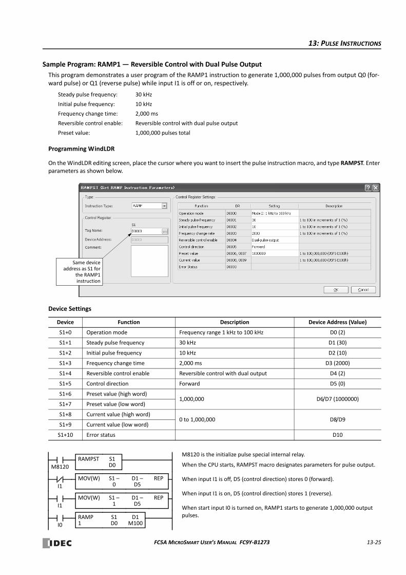
13: PULSE INSTRUCTIONS
Sample Program: RAMP1 — Reversible Control with Dual Pulse Output
This program demonstrates a user program of the RAMP1 instruction to generate 1,000,000 pulses from output Q0 (for‐ward pulse) or Q1 (reverse pulse) while input I1 is off or on, respectively.
Steady pulse frequency: 30 kHz
Initial pulse frequency: 10 kHz
Frequency change time: 2,000 ms
Reversible control enable: Reversible control with dual pulse output
Preset value: 1,000,000 pulses total
Programming WindLDR
On the WindLDR editing screen, place the cursor where you want to insert the pulse instruction macro, and type RAMPST. Enter parameters as shown below.
Device Settings
Device Function Description Device Address (Value)
S1+0 Operation mode Frequency range 1 kHz to 100 kHz D0 (2)
S1+1 Steady pulse frequency 30 kHz D1 (30)
S1+2 Initial pulse frequency 10 kHz D2 (10)
S1+3 Frequency change time 2,000 ms D3 (2000)
S1+4 Reversible control enable Reversible control with dual output D4 (2)
S1+5 Control direction Forward D5 (0)
S1+6 Preset value (high word)1,000,000 D6/D7 (1000000)
S1+7 Preset value (low word)
S1+8 Current value (high word)0 to 1,000,000 D8/D9
S1+9 Current value (low word)
S1+10 Error status D10
Same deviceaddress as S1 for
the RAMP1instruction
M8120
M8120 is the initialize pulse special internal relay.
When the CPU starts, RAMPST macro designates parameters for pulse output.
When input I1 is off, D5 (control direction) stores 0 (forward).
When input I1 is on, D5 (control direction) stores 1 (reverse).
When start input I0 is turned on, RAMP1 starts to generate 1,000,000 output pulses.
I0
D1M100
RAMP1
S1D0
REPS1 –0
MOV(W) D1 –D5
REPS1 –1
MOV(W) D1 –D5I1
I1
S1D0
RAMPST
FC5A MICROSMART USER’S MANUAL FC9Y‐B1273 13‐25
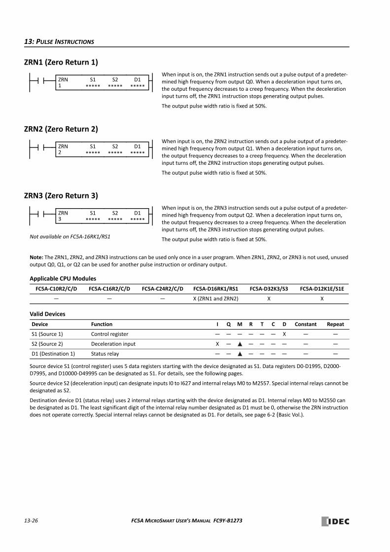
13: PULSE INSTRUCTIONS
ZRN1 (Zero Return 1)
ZRN2 (Zero Return 2)
ZRN3 (Zero Return 3)
Note: The ZRN1, ZRN2, and ZRN3 instructions can be used only once in a user program. When ZRN1, ZRN2, or ZRN3 is not used, unused output Q0, Q1, or Q2 can be used for another pulse instruction or ordinary output.
Applicable CPU Modules
Valid Devices
Source device S1 (control register) uses 5 data registers starting with the device designated as S1. Data registers D0‐D1995, D2000‐D7995, and D10000‐D49995 can be designated as S1. For details, see the following pages.
Source device S2 (deceleration input) can designate inputs I0 to I627 and internal relays M0 to M2557. Special internal relays cannot be designated as S2.
Destination device D1 (status relay) uses 2 internal relays starting with the device designated as D1. Internal relays M0 to M2550 can be designated as D1. The least significant digit of the internal relay number designated as D1 must be 0, otherwise the ZRN instruction does not operate correctly. Special internal relays cannot be designated as D1. For details, see page 6‐2 (Basic Vol.).
FC5A‐C10R2/C/D FC5A‐C16R2/C/D FC5A‐C24R2/C/D FC5A‐D16RK1/RS1 FC5A‐D32K3/S3 FC5A‐D12K1E/S1E
— — — X (ZRN1 and ZRN2) X X
Device Function I Q M R T C D Constant Repeat
S1 (Source 1) Control register — — — — — — X — —
S2 (Source 2) Deceleration input X — — — — — — —
D1 (Destination 1) Status relay — — — — — — — —
When input is on, the ZRN1 instruction sends out a pulse output of a predeter‐mined high frequency from output Q0. When a deceleration input turns on, the output frequency decreases to a creep frequency. When the deceleration input turns off, the ZRN1 instruction stops generating output pulses.
The output pulse width ratio is fixed at 50%.
ZRN1
S1*****
D1*****
S2*****
When input is on, the ZRN2 instruction sends out a pulse output of a predeter‐mined high frequency from output Q1. When a deceleration input turns on, the output frequency decreases to a creep frequency. When the deceleration input turns off, the ZRN2 instruction stops generating output pulses.
The output pulse width ratio is fixed at 50%.
ZRN2
S1*****
D1*****
S2*****
When input is on, the ZRN3 instruction sends out a pulse output of a predeter‐mined high frequency from output Q2. When a deceleration input turns on, the output frequency decreases to a creep frequency. When the deceleration input turns off, the ZRN3 instruction stops generating output pulses.
The output pulse width ratio is fixed at 50%.
ZRN3
S1*****
D1*****
S2*****
Not available on FC5A‐16RK1/RS1
13‐26 FC5A MICROSMART USER’S MANUAL FC9Y‐B1273
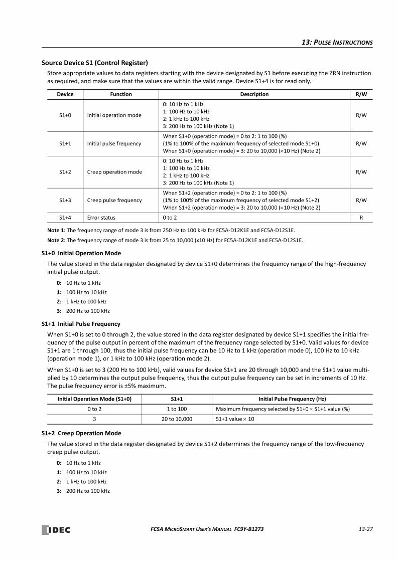
13: PULSE INSTRUCTIONS
Source Device S1 (Control Register)
Store appropriate values to data registers starting with the device designated by S1 before executing the ZRN instruction as required, and make sure that the values are within the valid range. Device S1+4 is for read only.
Note 1: The frequency range of mode 3 is from 250 Hz to 100 kHz for FC5A‐D12K1E and FC5A‐D12S1E.
Note 2: The frequency range of mode 3 is from 25 to 10,000 (x10 Hz) for FC5A‐D12K1E and FC5A‐D12S1E.
S1+0 Initial Operation Mode
The value stored in the data register designated by device S1+0 determines the frequency range of the high‐frequency initial pulse output.
0: 10 Hz to 1 kHz
1: 100 Hz to 10 kHz
2: 1 kHz to 100 kHz
3: 200 Hz to 100 kHz
S1+1 Initial Pulse Frequency
When S1+0 is set to 0 through 2, the value stored in the data register designated by device S1+1 specifies the initial fre‐quency of the pulse output in percent of the maximum of the frequency range selected by S1+0. Valid values for device S1+1 are 1 through 100, thus the initial pulse frequency can be 10 Hz to 1 kHz (operation mode 0), 100 Hz to 10 kHz (operation mode 1), or 1 kHz to 100 kHz (operation mode 2).
When S1+0 is set to 3 (200 Hz to 100 kHz), valid values for device S1+1 are 20 through 10,000 and the S1+1 value multi‐plied by 10 determines the output pulse frequency, thus the output pulse frequency can be set in increments of 10 Hz. The pulse frequency error is ±5% maximum.
S1+2 Creep Operation Mode
The value stored in the data register designated by device S1+2 determines the frequency range of the low‐frequency creep pulse output.
0: 10 Hz to 1 kHz
1: 100 Hz to 10 kHz
2: 1 kHz to 100 kHz
3: 200 Hz to 100 kHz
Device Function Description R/W
S1+0 Initial operation mode
0: 10 Hz to 1 kHz1: 100 Hz to 10 kHz2: 1 kHz to 100 kHz3: 200 Hz to 100 kHz (Note 1)
R/W
S1+1 Initial pulse frequencyWhen S1+0 (operation mode) = 0 to 2: 1 to 100 (%)(1% to 100% of the maximum frequency of selected mode S1+0)When S1+0 (operation mode) = 3: 20 to 10,000 (10 Hz) (Note 2)
R/W
S1+2 Creep operation mode
0: 10 Hz to 1 kHz1: 100 Hz to 10 kHz2: 1 kHz to 100 kHz3: 200 Hz to 100 kHz (Note 1)
R/W
S1+3 Creep pulse frequencyWhen S1+2 (operation mode) = 0 to 2: 1 to 100 (%)(1% to 100% of the maximum frequency of selected mode S1+2)When S1+2 (operation mode) = 3: 20 to 10,000 (10 Hz) (Note 2)
R/W
S1+4 Error status 0 to 2 R
Initial Operation Mode (S1+0) S1+1 Initial Pulse Frequency (Hz)
0 to 2 1 to 100 Maximum frequency selected by S1+0 S1+1 value (%)
3 20 to 10,000 S1+1 value 10
FC5A MICROSMART USER’S MANUAL FC9Y‐B1273 13‐27
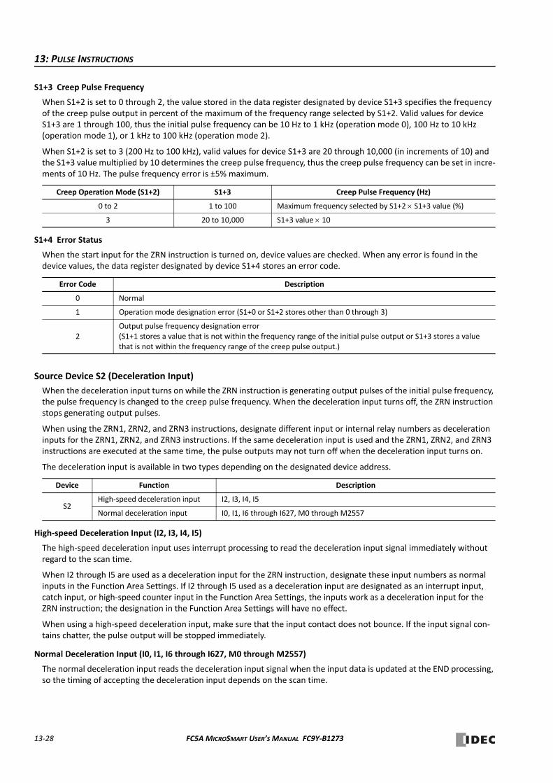
13: PULSE INSTRUCTIONS
S1+3 Creep Pulse Frequency
When S1+2 is set to 0 through 2, the value stored in the data register designated by device S1+3 specifies the frequency of the creep pulse output in percent of the maximum of the frequency range selected by S1+2. Valid values for device S1+3 are 1 through 100, thus the initial pulse frequency can be 10 Hz to 1 kHz (operation mode 0), 100 Hz to 10 kHz (operation mode 1), or 1 kHz to 100 kHz (operation mode 2).
When S1+2 is set to 3 (200 Hz to 100 kHz), valid values for device S1+3 are 20 through 10,000 (in increments of 10) and the S1+3 value multiplied by 10 determines the creep pulse frequency, thus the creep pulse frequency can be set in incre‐ments of 10 Hz. The pulse frequency error is ±5% maximum.
S1+4 Error Status
When the start input for the ZRN instruction is turned on, device values are checked. When any error is found in the device values, the data register designated by device S1+4 stores an error code.
Source Device S2 (Deceleration Input)
When the deceleration input turns on while the ZRN instruction is generating output pulses of the initial pulse frequency, the pulse frequency is changed to the creep pulse frequency. When the deceleration input turns off, the ZRN instruction stops generating output pulses.
When using the ZRN1, ZRN2, and ZRN3 instructions, designate different input or internal relay numbers as deceleration inputs for the ZRN1, ZRN2, and ZRN3 instructions. If the same deceleration input is used and the ZRN1, ZRN2, and ZRN3 instructions are executed at the same time, the pulse outputs may not turn off when the deceleration input turns on.
The deceleration input is available in two types depending on the designated device address.
High‐speed Deceleration Input (I2, I3, I4, I5)
The high‐speed deceleration input uses interrupt processing to read the deceleration input signal immediately without regard to the scan time.
When I2 through I5 are used as a deceleration input for the ZRN instruction, designate these input numbers as normal inputs in the Function Area Settings. If I2 through I5 used as a deceleration input are designated as an interrupt input, catch input, or high‐speed counter input in the Function Area Settings, the inputs work as a deceleration input for the ZRN instruction; the designation in the Function Area Settings will have no effect.
When using a high‐speed deceleration input, make sure that the input contact does not bounce. If the input signal con‐tains chatter, the pulse output will be stopped immediately.
Normal Deceleration Input (I0, I1, I6 through I627, M0 through M2557)
The normal deceleration input reads the deceleration input signal when the input data is updated at the END processing, so the timing of accepting the deceleration input depends on the scan time.
Creep Operation Mode (S1+2) S1+3 Creep Pulse Frequency (Hz)
0 to 2 1 to 100 Maximum frequency selected by S1+2 S1+3 value (%)
3 20 to 10,000 S1+3 value 10
Error Code Description
0 Normal
1 Operation mode designation error (S1+0 or S1+2 stores other than 0 through 3)
2Output pulse frequency designation error(S1+1 stores a value that is not within the frequency range of the initial pulse output or S1+3 stores a value that is not within the frequency range of the creep pulse output.)
Device Function Description
S2High‐speed deceleration input I2, I3, I4, I5
Normal deceleration input I0, I1, I6 through I627, M0 through M2557
13‐28 FC5A MICROSMART USER’S MANUAL FC9Y‐B1273
13: PULSE INSTRUCTIONS
Destination Device D1 (Status Relay)
Two internal relays starting with the device designated by D1 indicate the status of the ZRN instruction. These devices are for read only.
D1+0 Pulse Output ON
The internal relay designated by device D1+0 remains on while the ZRN instruction generates output pulses. When the start input or deceleration input for the ZRN instruction is turned off to stop generating output pulses, the internal relay designated by device D1+0 turns off.
D1+1 Pulse Output Complete
The internal relay designated by device D1+1 turns on when the deceleration input for the ZRN instruction is turned off to stop generating output pulses. When the start input for the ZRN instruction is turned on, the internal relay designated by device D1+1 turns off.
Device Function Description R/W
D1+0 Pulse output ON0: Pulse output OFF1: Pulse output ON
R
D1+1 Pulse output complete0: Pulse output not complete1: Pulse output complete
R
FC5A MICROSMART USER’S MANUAL FC9Y‐B1273 13‐29
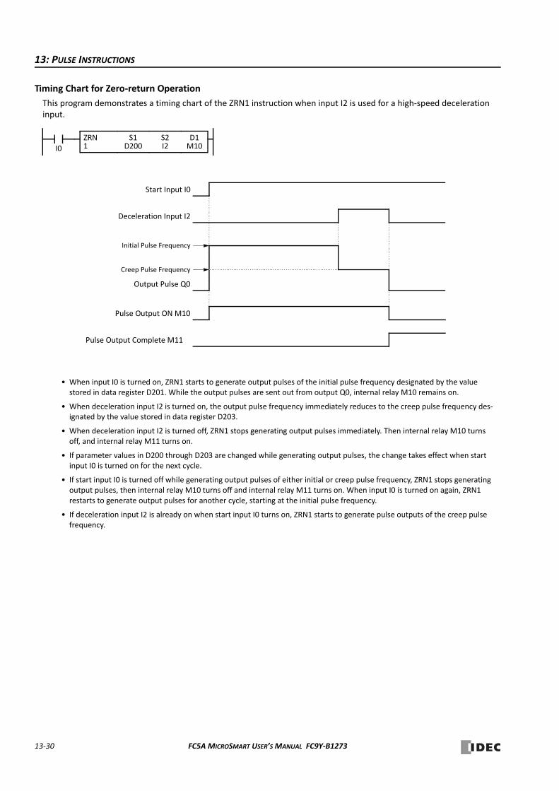
13: PULSE INSTRUCTIONS
Timing Chart for Zero‐return Operation
This program demonstrates a timing chart of the ZRN1 instruction when input I2 is used for a high‐speed deceleration input.
D1M10I0
ZRN1
S1D200
Output Pulse Q0
Deceleration Input I2
Start Input I0
• When input I0 is turned on, ZRN1 starts to generate output pulses of the initial pulse frequency designated by the value stored in data register D201. While the output pulses are sent out from output Q0, internal relay M10 remains on.
• When deceleration input I2 is turned on, the output pulse frequency immediately reduces to the creep pulse frequency des‐ignated by the value stored in data register D203.
• When deceleration input I2 is turned off, ZRN1 stops generating output pulses immediately. Then internal relay M10 turns off, and internal relay M11 turns on.
• If parameter values in D200 through D203 are changed while generating output pulses, the change takes effect when start input I0 is turned on for the next cycle.
• If start input I0 is turned off while generating output pulses of either initial or creep pulse frequency, ZRN1 stops generating output pulses, then internal relay M10 turns off and internal relay M11 turns on. When input I0 is turned on again, ZRN1 restarts to generate output pulses for another cycle, starting at the initial pulse frequency.
• If deceleration input I2 is already on when start input I0 turns on, ZRN1 starts to generate pulse outputs of the creep pulse frequency.
Pulse Output ON M10
Pulse Output Complete M11
S2I2
Initial Pulse Frequency
Creep Pulse Frequency
13‐30 FC5A MICROSMART USER’S MANUAL FC9Y‐B1273
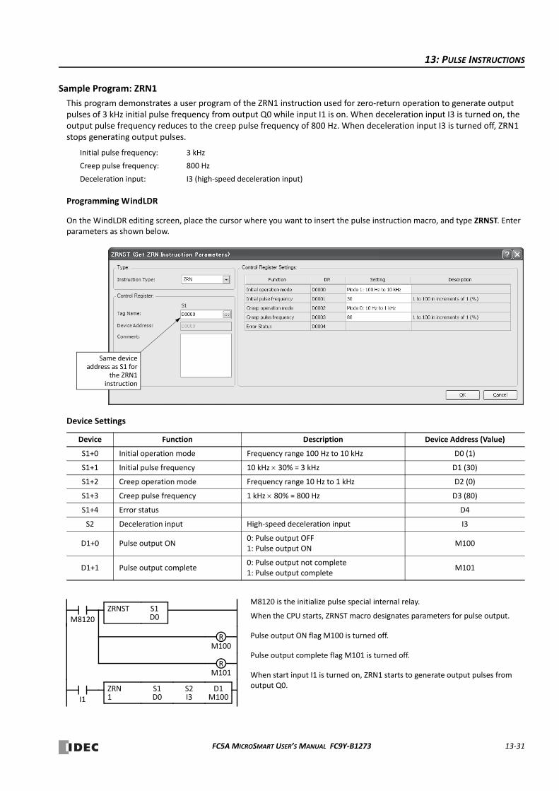
13: PULSE INSTRUCTIONS
Sample Program: ZRN1
This program demonstrates a user program of the ZRN1 instruction used for zero‐return operation to generate output pulses of 3 kHz initial pulse frequency from output Q0 while input I1 is on. When deceleration input I3 is turned on, the output pulse frequency reduces to the creep pulse frequency of 800 Hz. When deceleration input I3 is turned off, ZRN1 stops generating output pulses.
Initial pulse frequency: 3 kHz
Creep pulse frequency: 800 Hz
Deceleration input: I3 (high‐speed deceleration input)
Programming WindLDR
On the WindLDR editing screen, place the cursor where you want to insert the pulse instruction macro, and type ZRNST. Enter parameters as shown below.
Device Settings
Device Function Description Device Address (Value)
S1+0 Initial operation mode Frequency range 100 Hz to 10 kHz D0 (1)
S1+1 Initial pulse frequency 10 kHz 30% = 3 kHz D1 (30)
S1+2 Creep operation mode Frequency range 10 Hz to 1 kHz D2 (0)
S1+3 Creep pulse frequency 1 kHz 80% = 800 Hz D3 (80)
S1+4 Error status D4
S2 Deceleration input High‐speed deceleration input I3
D1+0 Pulse output ON0: Pulse output OFF1: Pulse output ON
M100
D1+1 Pulse output complete0: Pulse output not complete1: Pulse output complete
M101
Same deviceaddress as S1 for
the ZRN1instruction
M8120
M8120 is the initialize pulse special internal relay.
When the CPU starts, ZRNST macro designates parameters for pulse output.
Pulse output ON flag M100 is turned off.
Pulse output complete flag M101 is turned off.
When start input I1 is turned on, ZRN1 starts to generate output pulses from output Q0.
I1
D1M100
ZRN1
S1D0
M100R
M101R
S2I3
S1D0
ZRNST
FC5A MICROSMART USER’S MANUAL FC9Y‐B1273 13‐31

13: PULSE INSTRUCTIONS
13‐32 FC5A MICROSMART USER’S MANUAL FC9Y‐B1273

14: PID INSTRUCTION
IntroductionThe PID instruction implements a PID (proportional, integral, and derivative) algorithm with built‐in auto tuning to deter‐mine PID parameters, such as proportional gain, integral time, derivative time, and control action automatically. In addi‐tion, advanced auto tuning automatically determines the PID parameters without the need for designating auto tuning parameters.
The PID instruction is primarily designed for use with an analog I/O module to read analog input data, and turns on and off a designated output to perform PID control in applications such as temperature control described in the application example on page 14‐18. In addition, the PID instruction also generates an output manipulated variable for analog output module. When this device value is moved to an analog output module, a voltage (0 to 10V DC) or current (4 to 20 mA DC) output can be generated.
PID (PID Control)
Applicable CPU Modules and Quantity of PID InstructionsA maximum of 32 or 56 PID instructions can be used in a user program, depending on the CPU module type.
Special technical knowledge about the PID control is required to use the PID function of the MicroSmart. Use of the PID function without understanding the PID control may cause the MicroSmart to perform unexpected operation, resulting in disorder of the control system, damage, or accidents.
When using the PID instruction for feedback control, emergency stop and interlocking circuits must be configured outside the MicroSmart. If such a circuit is configured inside the MicroSmart, failure of inputting the process variable may cause equipment damage or accidents.
FC5A‐C10R2/C/D FC5A‐C16R2/C/D FC5A‐C24R2/C/D FC5A‐D16RK1/RS1 FC5A‐D32K3/S3 FC5A‐D12K1E/S1E
— — X (32) X (56) X (56) X (56)
Warning
When input is on, auto tuning and/or PID action is executed according to the value (0 through 4) stored in a data register device assigned for operation mode.
D1*****
S1*****
PID(*)0‐****
S2*****
S3*****
S4*****
FC5A MICROSMART USER’S MANUAL FC9Y‐B1273 14‐1

14: PID INSTRUCTION
Valid Devices
For the valid device address range, see pages 6‐1 and 6‐2 (Basic Vol.).
Source device S1 (control register) uses 27 data registers starting with the device designated by S1. Data registers D0‐D1973, D2000‐D7973, and D10000‐D49973 can be designated by S1. For details, see the following pages.
Source device S2 (control relay) uses 8 points of outputs or internal relays starting with the device designated by S2. Outputs Q0 through Q620 and internal relays M0 through M2550 can be designated by S2. For details, see page 14‐14.
Source device S3 (set point): When the linear conversion is disabled (S1+4 set to 0 or 2), the valid range of the set point (S3) is 0 through 4095 or 50,000 which can be designated using a data register or constant. When the linear conversion is enabled (S1+4 set to 1 or 3), the valid range is 0 to 65535 (word data type) or –32768 to 32767 (integer data type) that is a value after linear conversion. For details, see page 14‐16.
Source device S4 (process variable) is designated using a data register allocated as analog input data of the connected analog I/O mod‐ule. To read input data from an analog I/O module, designate a proper data register number depending on the slot position of the ana‐log I/O module and the analog input channel number connected to the analog input source. For details, see page 14‐16.
Source device S4 is compatible with the binary data type of analog input modules, ranging from 0 to 60,000.
Destination device D1 (manipulated variable) stores –32768 through 32767 that is a calculation result of the PID action. For details, see page 14‐16.
Module Type: Depending on the analog I/O module, select 0‐4095 or 0‐50000. These values determine the data range of the process variable (S4) and the output manipulated variable for analog output module (S1+24).
Data Type: When using an analog I/O module type of 0‐50000, select the data type from Word (W) or Integer (I). When using an analog I/O module type of 0‐4095, the data type is fixed at Integer (I). The data type selection has an effect on the set point (S4), the linear conversion maximum and minimum values (S1+5 and S1+6), the high and low alarm values (S1+14 and S1+15), the AT set point (S1+21), and the output manipulated value for analog output mode (S1+24).
Device Function I Q M R T C D Constant
S1 (Source 1) Control register — — — — — —D0‐D7973
D10000‐D49973—
S2 (Source 2) Control relay — Q0‐Q620 M0‐M2550 — — — — —
S3 (Source 3) Set point — — — — — —D0‐D7999
D10000‐D499990‐40950‐50000
S4 (Source 4)Process variable (before conversion)
— — — — — —D0‐D7999
D10000‐D49999—
D1 (Destination 1) Manipulated variable — — — — — —D0‐D7999
D10000‐D49999—
Module Type Depending on the analog I/O module, select 0‐4095 or 0‐50000.
Data Type Select the data type from Word (W) or Integer (I) when using analog module type 0‐50000.
Module Type Analog I/O Module
0‐4095
FC4A‐L03A1FC4A‐L03AP1FC4A‐J2A1FC4A‐K1A1FC4A‐K4A1
0‐50000
FC4A‐J4CN1FC4A‐J8C1FC4A‐J8AT1 (Note)FC4A‐K2C1
Note: The FC4A‐J8AT1 analog input module for PTC and NTC thermistors can be used only in the range where the thermis‐tor linearity is maintained.
14‐2 FC5A MICROSMART USER’S MANUAL FC9Y‐B1273
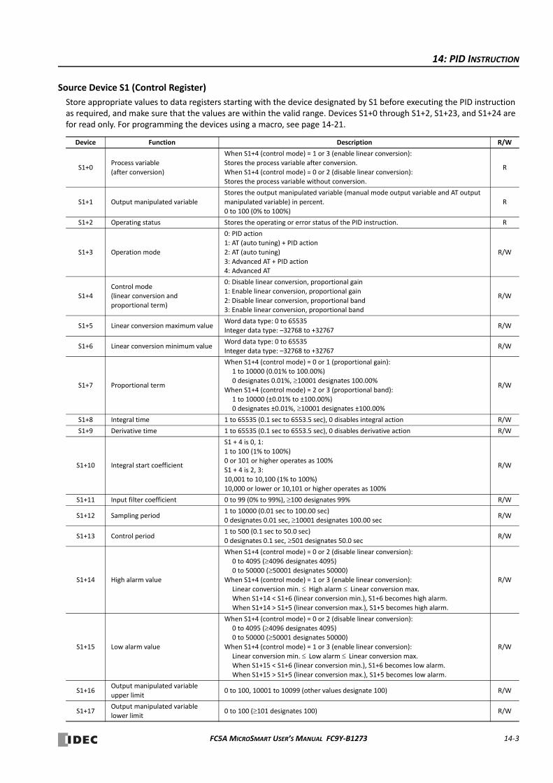
14: PID INSTRUCTION
Source Device S1 (Control Register)
Store appropriate values to data registers starting with the device designated by S1 before executing the PID instruction as required, and make sure that the values are within the valid range. Devices S1+0 through S1+2, S1+23, and S1+24 are for read only. For programming the devices using a macro, see page 14‐21.
Device Function Description R/W
S1+0Process variable
(after conversion)
When S1+4 (control mode) = 1 or 3 (enable linear conversion):
Stores the process variable after conversion.
When S1+4 (control mode) = 0 or 2 (disable linear conversion): Stores the process variable without conversion.
R
S1+1 Output manipulated variable
Stores the output manipulated variable (manual mode output variable and AT output
manipulated variable) in percent.
0 to 100 (0% to 100%)
R
S1+2 Operating status Stores the operating or error status of the PID instruction. R
S1+3 Operation mode
0: PID action1: AT (auto tuning) + PID action
2: AT (auto tuning)
3: Advanced AT + PID action4: Advanced AT
R/W
S1+4Control mode(linear conversion and
proportional term)
0: Disable linear conversion, proportional gain
1: Enable linear conversion, proportional gain
2: Disable linear conversion, proportional band3: Enable linear conversion, proportional band
R/W
S1+5 Linear conversion maximum valueWord data type: 0 to 65535
Integer data type: –32768 to +32767R/W
S1+6 Linear conversion minimum valueWord data type: 0 to 65535
Integer data type: –32768 to +32767R/W
S1+7 Proportional term
When S1+4 (control mode) = 0 or 1 (proportional gain):1 to 10000 (0.01% to 100.00%)
0 designates 0.01%, 10001 designates 100.00%When S1+4 (control mode) = 2 or 3 (proportional band):
1 to 10000 (±0.01% to ±100.00%)
0 designates ±0.01%, 10001 designates ±100.00%
R/W
S1+8 Integral time 1 to 65535 (0.1 sec to 6553.5 sec), 0 disables integral action R/W
S1+9 Derivative time 1 to 65535 (0.1 sec to 6553.5 sec), 0 disables derivative action R/W
S1+10 Integral start coefficient
S1 + 4 is 0, 1:
1 to 100 (1% to 100%)0 or 101 or higher operates as 100%
S1 + 4 is 2, 3:
10,001 to 10,100 (1% to 100%)
10,000 or lower or 10,101 or higher operates as 100%
R/W
S1+11 Input filter coefficient 0 to 99 (0% to 99%), 100 designates 99% R/W
S1+12 Sampling period1 to 10000 (0.01 sec to 100.00 sec)0 designates 0.01 sec, 10001 designates 100.00 sec
R/W
S1+13 Control period1 to 500 (0.1 sec to 50.0 sec)
0 designates 0.1 sec, 501 designates 50.0 secR/W
S1+14 High alarm value
When S1+4 (control mode) = 0 or 2 (disable linear conversion):
0 to 4095 (4096 designates 4095)0 to 50000 (50001 designates 50000)
When S1+4 (control mode) = 1 or 3 (enable linear conversion):
Linear conversion min. High alarm Linear conversion max.When S1+14 < S1+6 (linear conversion min.), S1+6 becomes high alarm.
When S1+14 > S1+5 (linear conversion max.), S1+5 becomes high alarm.
R/W
S1+15 Low alarm value
When S1+4 (control mode) = 0 or 2 (disable linear conversion):
0 to 4095 (4096 designates 4095)0 to 50000 (50001 designates 50000)
When S1+4 (control mode) = 1 or 3 (enable linear conversion):
Linear conversion min. Low alarm Linear conversion max.When S1+15 < S1+6 (linear conversion min.), S1+6 becomes low alarm.
When S1+15 > S1+5 (linear conversion max.), S1+5 becomes low alarm.
R/W
S1+16Output manipulated variable
upper limit0 to 100, 10001 to 10099 (other values designate 100) R/W
S1+17Output manipulated variable lower limit
0 to 100 (101 designates 100) R/W
FC5A MICROSMART USER’S MANUAL FC9Y‐B1273 14‐3
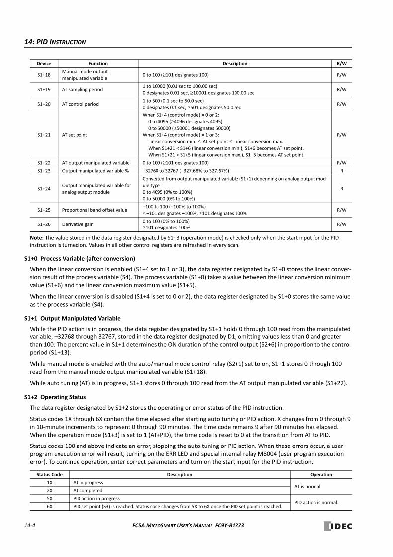
14: PID INSTRUCTION
Note: The value stored in the data register designated by S1+3 (operation mode) is checked only when the start input for the PID instruction is turned on. Values in all other control registers are refreshed in every scan.
S1+0 Process Variable (after conversion)
When the linear conversion is enabled (S1+4 set to 1 or 3), the data register designated by S1+0 stores the linear conver‐sion result of the process variable (S4). The process variable (S1+0) takes a value between the linear conversion minimum value (S1+6) and the linear conversion maximum value (S1+5).
When the linear conversion is disabled (S1+4 is set to 0 or 2), the data register designated by S1+0 stores the same value as the process variable (S4).
S1+1 Output Manipulated Variable
While the PID action is in progress, the data register designated by S1+1 holds 0 through 100 read from the manipulated variable, –32768 through 32767, stored in the data register designated by D1, omitting values less than 0 and greater than 100. The percent value in S1+1 determines the ON duration of the control output (S2+6) in proportion to the control period (S1+13).
While manual mode is enabled with the auto/manual mode control relay (S2+1) set to on, S1+1 stores 0 through 100 read from the manual mode output manipulated variable (S1+18).
While auto tuning (AT) is in progress, S1+1 stores 0 through 100 read from the AT output manipulated variable (S1+22).
S1+2 Operating Status
The data register designated by S1+2 stores the operating or error status of the PID instruction.
Status codes 1X through 6X contain the time elapsed after starting auto tuning or PID action. X changes from 0 through 9 in 10‐minute increments to represent 0 through 90 minutes. The time code remains 9 after 90 minutes has elapsed. When the operation mode (S1+3) is set to 1 (AT+PID), the time code is reset to 0 at the transition from AT to PID.
Status codes 100 and above indicate an error, stopping the auto tuning or PID action. When these errors occur, a user program execution error will result, turning on the ERR LED and special internal relay M8004 (user program execution error). To continue operation, enter correct parameters and turn on the start input for the PID instruction.
S1+18Manual mode output
manipulated variable0 to 100 (101 designates 100) R/W
S1+19 AT sampling period1 to 10000 (0.01 sec to 100.00 sec)
0 designates 0.01 sec, 10001 designates 100.00 secR/W
S1+20 AT control period1 to 500 (0.1 sec to 50.0 sec)0 designates 0.1 sec, 501 designates 50.0 sec
R/W
S1+21 AT set point
When S1+4 (control mode) = 0 or 2:
0 to 4095 (4096 designates 4095)0 to 50000 (50001 designates 50000)
When S1+4 (control mode) = 1 or 3:
Linear conversion min. AT set point Linear conversion max.
When S1+21 < S1+6 (linear conversion min.), S1+6 becomes AT set point.When S1+21 > S1+5 (linear conversion max.), S1+5 becomes AT set point.
R/W
S1+22 AT output manipulated variable 0 to 100 (101 designates 100) R/W
S1+23 Output manipulated variable % –32768 to 32767 (–327.68% to 327.67%) R
S1+24Output manipulated variable for
analog output module
Converted from output manipulated variable (S1+1) depending on analog output mod‐
ule type
0 to 4095 (0% to 100%)0 to 50000 (0% to 100%)
R
S1+25 Proportional band offset value–100 to 100 (–100% to 100%)
–101 designates –100%, 101 designates 100%R/W
S1+26 Derivative gain0 to 100 (0% to 100%)
101 designates 100%R/W
Status Code Description Operation
1X AT in progressAT is normal.
2X AT completed
5X PID action in progressPID action is normal.
6X PID set point (S3) is reached. Status code changes from 5X to 6X once the PID set point is reached.
Device Function Description R/W
14‐4 FC5A MICROSMART USER’S MANUAL FC9Y‐B1273
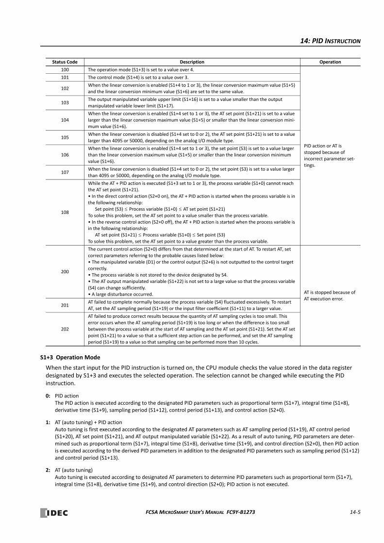
14: PID INSTRUCTION
S1+3 Operation Mode
When the start input for the PID instruction is turned on, the CPU module checks the value stored in the data register designated by S1+3 and executes the selected operation. The selection cannot be changed while executing the PID instruction.
0: PID actionThe PID action is executed according to the designated PID parameters such as proportional term (S1+7), integral time (S1+8), derivative time (S1+9), sampling period (S1+12), control period (S1+13), and control action (S2+0).
1: AT (auto tuning) + PID actionAuto tuning is first executed according to the designated AT parameters such as AT sampling period (S1+19), AT control period (S1+20), AT set point (S1+21), and AT output manipulated variable (S1+22). As a result of auto tuning, PID parameters are deter‐mined such as proportional term (S1+7), integral time (S1+8), derivative time (S1+9), and control direction (S2+0), then PID action is executed according to the derived PID parameters in addition to the designated PID parameters such as sampling period (S1+12) and control period (S1+13).
2: AT (auto tuning)Auto tuning is executed according to designated AT parameters to determine PID parameters such as proportional term (S1+7), integral time (S1+8), derivative time (S1+9), and control direction (S2+0); PID action is not executed.
100 The operation mode (S1+3) is set to a value over 4.
PID action or AT is
stopped because of incorrect parameter set‐
tings.
101 The control mode (S1+4) is set to a value over 3.
102When the linear conversion is enabled (S1+4 to 1 or 3), the linear conversion maximum value (S1+5)
and the linear conversion minimum value (S1+6) are set to the same value.
103The output manipulated variable upper limit (S1+16) is set to a value smaller than the output
manipulated variable lower limit (S1+17).
104When the linear conversion is enabled (S1+4 set to 1 or 3), the AT set point (S1+21) is set to a value larger than the linear conversion maximum value (S1+5) or smaller than the linear conversion mini‐
mum value (S1+6).
105When the linear conversion is disabled (S1+4 set to 0 or 2), the AT set point (S1+21) is set to a value
larger than 4095 or 50000, depending on the analog I/O module type.
106When the linear conversion is enabled (S1+4 set to 1 or 3), the set point (S3) is set to a value larger than the linear conversion maximum value (S1+5) or smaller than the linear conversion minimum
value (S1+6).
107When the linear conversion is disabled (S1+4 set to 0 or 2), the set point (S3) is set to a value larger
than 4095 or 50000, depending on the analog I/O module type.
108
While the AT + PID action is executed (S1+3 set to 1 or 3), the process variable (S1+0) cannot reach the AT set point (S1+21).
• In the direct control action (S2+0 on), the AT + PID action is started when the process variable is in
the following relationship: Set point (S3) Process variable (S1+0) AT set point (S1+21)
To solve this problem, set the AT set point to a value smaller than the process variable.
• In the reverse control action (S2+0 off), the AT + PID action is started when the process variable is in the following relationship:
AT set point (S1+21) Process variable (S1+0) Set point (S3)
To solve this problem, set the AT set point to a value greater than the process variable.
200
The current control action (S2+0) differs from that determined at the start of AT. To restart AT, set correct parameters referring to the probable causes listed below:
• The manipulated variable (D1) or the control output (S2+6) is not outputted to the control target
correctly.• The process variable is not stored to the device designated by S4.
• The AT output manipulated variable (S1+22) is not set to a large value so that the process variable
(S4) can change sufficiently.• A large disturbance occurred. AT is stopped because of
AT execution error.
201AT failed to complete normally because the process variable (S4) fluctuated excessively. To restart
AT, set the AT sampling period (S1+19) or the input filter coefficient (S1+11) to a larger value.
202
AT failed to produce correct results because the quantity of AT sampling cycles is too small. This
error occurs when the AT sampling period (S1+19) is too long or when the difference is too small between the process variable at the start of AT sampling and the AT set point (S1+21). Set the AT set
point (S1+21) to a value so that a sufficient step action can be performed, and set the AT sampling
period (S1+19) to a value so that sampling can be performed more than 10 cycles.
Status Code Description Operation
FC5A MICROSMART USER’S MANUAL FC9Y‐B1273 14‐5
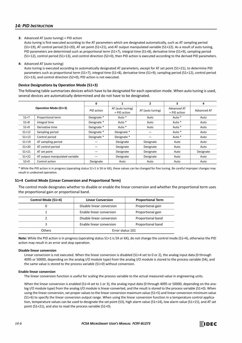
14: PID INSTRUCTION
3: Advanced AT (auto tuning) + PID actionAuto tuning is first executed according to the AT parameters which are designated automatically, such as AT sampling period (S1+19), AT control period (S1+20), AT set point (S1+21), and AT output manipulated variable (S1+22). As a result of auto tuning, PID parameters are determined such as proportional term (S1+7), integral time (S1+8), derivative time (S1+9), sampling period (S1+12), control period (S1+13), and control direction (S2+0), then PID action is executed according to the derived PID parameters.
4: Advanced AT (auto tuning)Auto tuning is executed according to automatically designated AT parameters, except for AT set point (S1+21), to determine PID parameters such as proportional term (S1+7), integral time (S1+8), derivative time (S1+9), sampling period (S1+12), control period (S1+13), and control direction (S2+0); PID action is not executed.
Device Designations by Operation Mode (S1+3)
The following table summarizes devices which have to be designated for each operation mode. When auto tuning is used, several devices are automatically determined and do not have to be designated.
* While the PID action is in progress (operating status S1+1 is 5X or 6X), these values can be changed for fine tuning. Be careful improper changes may result in undesired operation.
S1+4 Control Mode (Linear Conversion and Proportional Term)
The control mode designates whether to disable or enable the linear conversion and whether the proportional term uses the proportional gain or proportional band.
Note: While the PID action is in progress (operating status S1+1 is 5X or 6X), do not change the control mode (S1+4), otherwise the PID action may result in an error and stop operation.
Disable linear conversionLinear conversion is not executed. When the linear conversion is disabled (S1+4 set to 0 or 2), the analog input data (0 through 4095 or 50000, depending on the analog I/O module type) from the analog I/O module is stored to the process variable (S4), and the same value is stored to the process variable (S1+0) without conversion.
Enable linear conversionThe linear conversion function is useful for scaling the process variable to the actual measured value in engineering units.
When the linear conversion is enabled (S1+4 set to 1 or 3), the analog input data (0 through 4095 or 50000, depending on the ana‐log I/O module type) from the analog I/O module is linear‐converted, and the result is stored to the process variable (S1+0). When using the linear conversion, set proper values to the linear conversion maximum value (S1+5) and linear conversion minimum value (S1+6) to specify the linear conversion output range. When using the linear conversion function in a temperature control applica‐tion, temperature values can be used to designate the set point (S3), high alarm value (S1+14), low alarm value (S1+15), and AT set point (S1+21), and also to read the process variable (S1+0).
Operation Mode (S1+3)
0 1 2 3 4
PID actionAT (auto tuning) + PID action
AT (auto tuning)Advanced AT + PID action
Advanced AT
S1+7 Proportional term Designate * Auto * Auto Auto * Auto
S1+8 Integral time Designate * Auto * Auto Auto * Auto
S1+9 Derivative time Designate * Auto * Auto Auto * Auto
S1+12 Sampling period Designate * Designate * — Auto * Auto
S1+13 Control period Designate * Designate * — Auto * Auto
S1+19 AT sampling period — Designate Designate Auto Auto
S1+20 AT control period — Designate Designate Auto Auto
S1+21 AT set point — Designate Designate Auto Designate
S1+22 AT output manipulated variable — Designate Designate Auto Auto
S2+0 Control action Designate Auto Auto Auto Auto
Control Mode (S1+4) Linear Conversion Proportional Term
0 Disable linear conversion Proportional gain
1 Enable linear conversion Proportional gain
2 Disable linear conversion Proportional band
3 Enable linear conversion Proportional band
Others Error status 101
14‐6 FC5A MICROSMART USER’S MANUAL FC9Y‐B1273
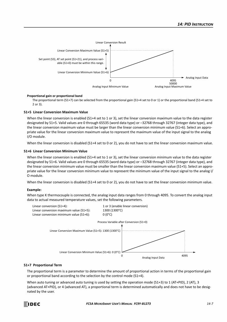
14: PID INSTRUCTION
Proportional gain or proportional bandThe proportional term (S1+7) can be selected from the proportional gain (S1+4 set to 0 or 1) or the proportional band (S1+4 set to 2 or 3).
S1+5 Linear Conversion Maximum Value
When the linear conversion is enabled (S1+4 set to 1 or 3), set the linear conversion maximum value to the data register designated by S1+5. Valid values are 0 through 65535 (word data type) or –32768 through 32767 (integer data type), and the linear conversion maximum value must be larger than the linear conversion minimum value (S1+6). Select an appro‐priate value for the linear conversion maximum value to represent the maximum value of the input signal to the analog I/O module.
When the linear conversion is disabled (S1+4 set to 0 or 2), you do not have to set the linear conversion maximum value.
S1+6 Linear Conversion Minimum Value
When the linear conversion is enabled (S1+4 set to 1 or 3), set the linear conversion minimum value to the data register designated by S1+6. Valid values are 0 through 65535 (word data type) or –32768 through 32767 (integer data type), and the linear conversion minimum value must be smaller than the linear conversion maximum value (S1+5). Select an appro‐priate value for the linear conversion minimum value to represent the minimum value of the input signal to the analog I/O module.
When the linear conversion is disabled (S1+4 set to 0 or 2), you do not have to set the linear conversion minimum value.
Example:
When type K thermocouple is connected, the analog input data ranges from 0 through 4095. To convert the analog input data to actual measured temperature values, set the following parameters.
Linear conversion (S1+4): 1 or 3 (enable linear conversion)Linear conversion maximum value (S1+5): 1300 (1300°C)Linear conversion minimum value (S1+6): 0 (0°C)
S1+7 Proportional Term
The proportional term is a parameter to determine the amount of proportional action in terms of the proportional gain or proportional band according to the selection by the control mode (S1+4).
When auto tuning or advanced auto tuning is used by setting the operation mode (S1+3) to 1 (AT+PID), 2 (AT), 3 (advanced AT+PID), or 4 (advanced AT), a proportional term is determined automatically and does not have to be desig‐nated by the user.
Linear Conversion Result
0Analog Input Data
Linear Conversion Maximum Value (S1+5)
Linear Conversion Minimum Value (S1+6)
4095
Set point (S3), AT set point (S1+21), and process vari‐
able (S1+0) must be within this range.
50000Analog Input Maximum ValueAnalog Input Minimum Value
Process Variable after Conversion (S1+0)
Analog Input Data
Linear Conversion Maximum Value (S1+5): 1300 (1300°C)
Linear Conversion Minimum Value (S1+6): 0 (0°C)40950
FC5A MICROSMART USER’S MANUAL FC9Y‐B1273 14‐7
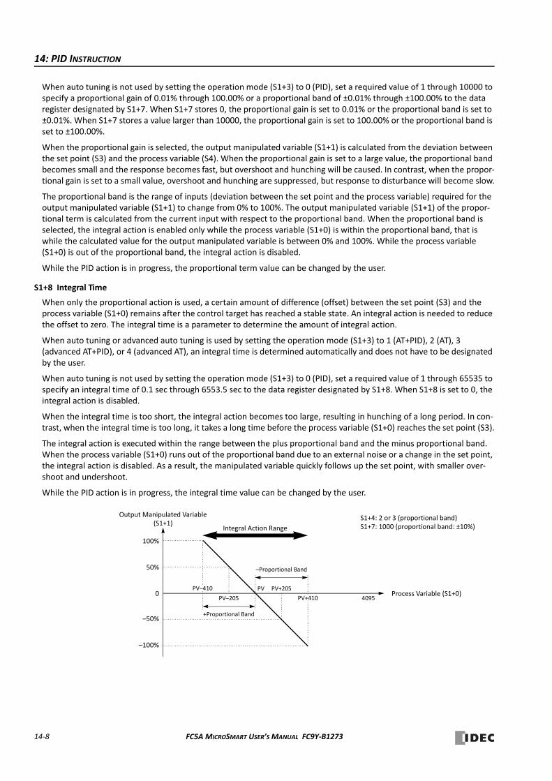
14: PID INSTRUCTION
When auto tuning is not used by setting the operation mode (S1+3) to 0 (PID), set a required value of 1 through 10000 to specify a proportional gain of 0.01% through 100.00% or a proportional band of ±0.01% through ±100.00% to the data register designated by S1+7. When S1+7 stores 0, the proportional gain is set to 0.01% or the proportional band is set to ±0.01%. When S1+7 stores a value larger than 10000, the proportional gain is set to 100.00% or the proportional band is set to ±100.00%.
When the proportional gain is selected, the output manipulated variable (S1+1) is calculated from the deviation between the set point (S3) and the process variable (S4). When the proportional gain is set to a large value, the proportional band becomes small and the response becomes fast, but overshoot and hunching will be caused. In contrast, when the propor‐tional gain is set to a small value, overshoot and hunching are suppressed, but response to disturbance will become slow.
The proportional band is the range of inputs (deviation between the set point and the process variable) required for the output manipulated variable (S1+1) to change from 0% to 100%. The output manipulated variable (S1+1) of the propor‐tional term is calculated from the current input with respect to the proportional band. When the proportional band is selected, the integral action is enabled only while the process variable (S1+0) is within the proportional band, that is while the calculated value for the output manipulated variable is between 0% and 100%. While the process variable (S1+0) is out of the proportional band, the integral action is disabled.
While the PID action is in progress, the proportional term value can be changed by the user.
S1+8 Integral Time
When only the proportional action is used, a certain amount of difference (offset) between the set point (S3) and the process variable (S1+0) remains after the control target has reached a stable state. An integral action is needed to reduce the offset to zero. The integral time is a parameter to determine the amount of integral action.
When auto tuning or advanced auto tuning is used by setting the operation mode (S1+3) to 1 (AT+PID), 2 (AT), 3 (advanced AT+PID), or 4 (advanced AT), an integral time is determined automatically and does not have to be designated by the user.
When auto tuning is not used by setting the operation mode (S1+3) to 0 (PID), set a required value of 1 through 65535 to specify an integral time of 0.1 sec through 6553.5 sec to the data register designated by S1+8. When S1+8 is set to 0, the integral action is disabled.
When the integral time is too short, the integral action becomes too large, resulting in hunching of a long period. In con‐trast, when the integral time is too long, it takes a long time before the process variable (S1+0) reaches the set point (S3).
The integral action is executed within the range between the plus proportional band and the minus proportional band. When the process variable (S1+0) runs out of the proportional band due to an external noise or a change in the set point, the integral action is disabled. As a result, the manipulated variable quickly follows up the set point, with smaller over‐shoot and undershoot.
While the PID action is in progress, the integral time value can be changed by the user.
4095PV–205
PV PV+205
+Proportional Band
–Proportional Band
PV+410
PV–410Process Variable (S1+0)
Integral Action Range
S1+4: 2 or 3 (proportional band)S1+7: 1000 (proportional band: ±10%)
Output Manipulated Variable
100%
0
(S1+1)
50%
–50%
–100%
14‐8 FC5A MICROSMART USER’S MANUAL FC9Y‐B1273

14: PID INSTRUCTION
S1+9 Derivative Time
The derivative action is a function to adjust the process variable (S1+0) to the set point (S3) by increasing the manipulated variable (D1) when the set point (S3) is changed or when the difference between the process variable (S1+0) and the set point (S3) is increased due to disturbance. The derivative time is a parameter to determine the amount of derivative action.
When auto tuning is used by setting the operation mode (S1+3) to 1 (AT+PID), 2 (AT), 3 (advanced AT+PID), or 4 (advanced AT), a derivative time is determined automatically and does not have to be designated by the user.
When auto tuning is not used by setting the operation mode (S1+3) to 0 (PID), set a required value of 1 through 65535 to specify a derivative time of 0.1 sec through 6553.5 sec to the data register designated by S1+9. When S1+9 is set to 0, the derivative action is disabled.
When the derivative time is set to a large value, the derivative action becomes large. When the derivative action is too large, hunching of a short period is caused.
While the PID action is in progress, the derivative time value can be changed by the user.
S1+10 Integral Start Coefficient
The integral start coefficient specifies the threshold value to start the integral action. If the integral action is enabled from the start of execution of the PID instruction, this may cause the process variable to be overshot. Overshooting can be controlled by delaying the start of the integral action with the integral start coefficient linked to the proportional term. If the integral start coefficient is too small, overshooting is eliminated, but a certain amount of difference (offset) between the set point and the process variable may occur. If the integral start coefficient is too large, the offset becomes smaller, but overshooting may occur. To enable the integral start coefficient, turn off the integral start coefficient disable relay (S2+3). To disable the integral start coefficient, turn on the integral start coefficient disable relay (S2+3).
When the control mode (S1+4) proportional term is proportional gain:Specify a value between 1 and 100 (1% to 100%). 0 or 101 or higher operates as 100%.
When the control mode (S1+4) proportional term is proportional band:The operation in regard to the preset value differs according to the system program version as detailed in the following table.
S1+11 Input Filter Coefficient
The input filter has an effect to smooth out fluctuations of the process variable (S4). Set a required value of 0 through 99 to specify an input filter coefficient of 0% through 99% to the data register designated by S1+11. When S1+11 stores a value larger than 99, the input filter coefficient is set to 99%. The larger the coefficient, the larger the input filter effect.
The input filter is effective for reading a process variable (S4) such as temperature data when the value changes at each sampling time. The input filter coefficient is in effect during auto tuning and PID action.
CPU modules System program version Operation
FC5A‐C10R2xFC5A‐C16R2xFC5A‐C24R2xFC5A‐D16Rx1FC5A‐D32x3
245 or lower This preset value is not used. The integral start coefficient always operates as 100%.
246 or higherSpecify a value between 10,001 and 10,100 (1% to 100%).10,000 or lower or 10,101 or higher operates as 100%
FC5A‐D12x1E
130 or lower This preset value is not used. The integral start coefficient always operates as 100%.
131 or higherSpecify a value between 10,001 and 10,100 (1% to 100%).10,000 or lower or 10,101 or higher operates as 100%
Process Variable
When the integral start coefficient is large When the integral start coefficient is small
Set Point
TimeReverse Control Ac�on
Process Variable
Set Point
TimeReverse Control Ac�on
FC5A MICROSMART USER’S MANUAL FC9Y‐B1273 14‐9
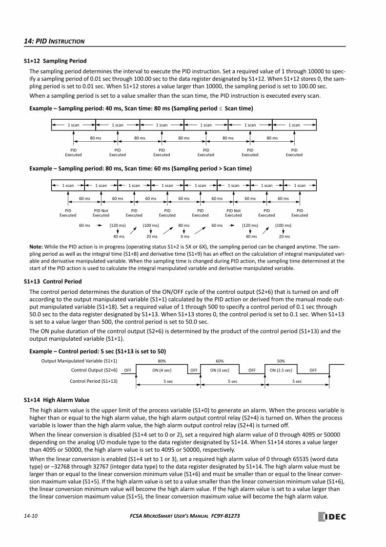
14: PID INSTRUCTION
S1+12 Sampling Period
The sampling period determines the interval to execute the PID instruction. Set a required value of 1 through 10000 to spec‐ify a sampling period of 0.01 sec through 100.00 sec to the data register designated by S1+12. When S1+12 stores 0, the sam‐pling period is set to 0.01 sec. When S1+12 stores a value larger than 10000, the sampling period is set to 100.00 sec.
When a sampling period is set to a value smaller than the scan time, the PID instruction is executed every scan.
Example – Sampling period: 40 ms, Scan time: 80 ms (Sampling period Scan time)
Example – Sampling period: 80 ms, Scan time: 60 ms (Sampling period > Scan time)
Note: While the PID action is in progress (operating status S1+2 is 5X or 6X), the sampling period can be changed anytime. The sam‐pling period as well as the integral time (S1+8) and derivative time (S1+9) has an effect on the calculation of integral manipulated vari‐able and derivative manipulated variable. When the sampling time is changed during PID action, the sampling time determined at the start of the PID action is used to calculate the integral manipulated variable and derivative manipulated variable.
S1+13 Control Period
The control period determines the duration of the ON/OFF cycle of the control output (S2+6) that is turned on and off according to the output manipulated variable (S1+1) calculated by the PID action or derived from the manual mode out‐put manipulated variable (S1+18). Set a required value of 1 through 500 to specify a control period of 0.1 sec through 50.0 sec to the data register designated by S1+13. When S1+13 stores 0, the control period is set to 0.1 sec. When S1+13 is set to a value larger than 500, the control period is set to 50.0 sec.
The ON pulse duration of the control output (S2+6) is determined by the product of the control period (S1+13) and the output manipulated variable (S1+1).
Example – Control period: 5 sec (S1+13 is set to 50)
S1+14 High Alarm Value
The high alarm value is the upper limit of the process variable (S1+0) to generate an alarm. When the process variable is higher than or equal to the high alarm value, the high alarm output control relay (S2+4) is turned on. When the process variable is lower than the high alarm value, the high alarm output control relay (S2+4) is turned off.
When the linear conversion is disabled (S1+4 set to 0 or 2), set a required high alarm value of 0 through 4095 or 50000 depending on the analog I/O module type to the data register designated by S1+14. When S1+14 stores a value larger than 4095 or 50000, the high alarm value is set to 4095 or 50000, respectively.
When the linear conversion is enabled (S1+4 set to 1 or 3), set a required high alarm value of 0 through 65535 (word data type) or –32768 through 32767 (integer data type) to the data register designated by S1+14. The high alarm value must be larger than or equal to the linear conversion minimum value (S1+6) and must be smaller than or equal to the linear conver‐sion maximum value (S1+5). If the high alarm value is set to a value smaller than the linear conversion minimum value (S1+6), the linear conversion minimum value will become the high alarm value. If the high alarm value is set to a value larger than the linear conversion maximum value (S1+5), the linear conversion maximum value will become the high alarm value.
1 scan
80 ms 80 ms 80 ms 80 ms 80 ms
PIDExecuted
PIDExecuted
PIDExecuted
PIDExecuted
PIDExecuted
PIDExecuted
1 scan 1 scan 1 scan 1 scan 1 scan
60 ms
1 scan
60 ms 60 ms 60 ms 60 ms 60 ms 60 ms
PID
60 ms (120 ms)
40 ms
(100 ms)
20 ms
80 ms
0 ms
60 ms (120 ms)
40 ms
(100 ms)
20 ms
1 scan 1 scan 1 scan 1 scan 1 scan 1 scan 1 scan
ExecutedPID NotExecuted
PIDExecuted
PIDExecuted
PIDExecuted
PID NotExecuted
PIDExecuted
PIDExecuted
5 sec 5 sec 5 sec
ON (4 sec) OFF ON (3 sec) ON (2.5 sec)OFF OFFOFFControl Output (S2+6)
80% 60% 50%Output Manipulated Variable (S1+1)
Control Period (S1+13)
14‐10 FC5A MICROSMART USER’S MANUAL FC9Y‐B1273
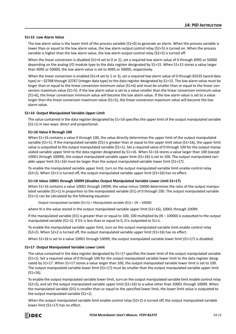
14: PID INSTRUCTION
S1+15 Low Alarm Value
The low alarm value is the lower limit of the process variable (S1+0) to generate an alarm. When the process variable is lower than or equal to the low alarm value, the low alarm output control relay (S2+5) is turned on. When the process variable is higher than the low alarm value, the low alarm output control relay (S2+5) is turned off.
When the linear conversion is disabled (S1+4 set to 0 or 2), set a required low alarm value of 0 through 4095 or 50000 depending on the analog I/O module type to the data register designated by S1+15. When S1+15 stores a value larger than 4095 or 50000, the low alarm value is set to 4095 or 50000, respectively.
When the linear conversion is enabled (S1+4 set to 1 or 3), set a required low alarm value of 0 through 65535 (word data type) or –32768 through 32767 (integer data type) to the data register designated by S1+15. The low alarm value must be larger than or equal to the linear conversion minimum value (S1+6) and must be smaller than or equal to the linear con‐version maximum value (S1+5). If the low alarm value is set to a value smaller than the linear conversion minimum value (S1+6), the linear conversion minimum value will become the low alarm value. If the low alarm value is set to a value larger than the linear conversion maximum value (S1+5), the linear conversion maximum value will become the low alarm value.
S1+16 Output Manipulated Variable Upper Limit
The value contained in the data register designated by S1+16 specifies the upper limit of the output manipulated variable (S1+1) in two ways: direct and proportional.
S1+16 Value 0 through 100
When S1+16 contains a value 0 through 100, the value directly determines the upper limit of the output manipulated variable (S1+1). If the manipulated variable (D1) is greater than or equal to the upper limit value (S1+16), the upper limit value is outputted to the output manipulated variable (S1+1). Set a required value of 0 through 100 for the output manip‐ulated variable upper limit to the data register designated by S1+16. When S1+16 stores a value larger than 100 (except 10001 through 10099), the output manipulated variable upper limit (S1+16) is set to 100. The output manipulated vari‐able upper limit (S1+16) must be larger than the output manipulated variable lower limit (S1+17).
To enable the manipulated variable upper limit, turn on the output manipulated variable limit enable control relay (S2+2). When S2+2 is turned off, the output manipulated variable upper limit (S1+16) has no effect.
S1+16 Value 10001 through 10099 (disables Output Manipulated Variable Lower Limit S1+17)
When S1+16 contains a value 10001 through 10099, the value minus 10000 determines the ratio of the output manipu‐lated variable (S1+1) in proportion to the manipulated variable (D1) of 0 through 100. The output manipulated variable (S1+1) can be calculated by the following equation:
Output manipulated variable (S1+1) = Manipulated variable (D1) (N – 10000)
where N is the value stored in the output manipulated variable upper limit (S1+16), 10001 through 10099.
If the manipulated variable (D1) is greater than or equal to 100, 100 multiplied by (N – 10000) is outputted to the output manipulated variable (S1+1). If D1 is less than or equal to 0, 0 is outputted to S1+1.
To enable the manipulated variable upper limit, turn on the output manipulated variable limit enable control relay (S2+2). When S2+2 is turned off, the output manipulated variable upper limit (S1+16) has no effect.
When S1+16 is set to a value 10001 through 10099, the output manipulated variable lower limit (S1+17) is disabled.
S1+17 Output Manipulated Variable Lower Limit
The value contained in the data register designated by S1+17 specifies the lower limit of the output manipulated variable (S1+1). Set a required value of 0 through 100 for the output manipulated variable lower limit to the data register desig‐nated by S1+17. When S1+17 stores a value larger than 100, the output manipulated variable lower limit is set to 100. The output manipulated variable lower limit (S1+17) must be smaller than the output manipulated variable upper limit (S1+16).
To enable the output manipulated variable lower limit, turn on the output manipulated variable limit enable control relay (S2+2), and set the output manipulated variable upper limit (S1+16) to a value other than 10001 through 10099. When the manipulated variable (D1) is smaller than or equal to the specified lower limit, the lower limit value is outputted to the output manipulated variable (S1+1).
When the output manipulated variable limit enable control relay (S2+2) is turned off, the output manipulated variable lower limit (S1+17) has no effect.
FC5A MICROSMART USER’S MANUAL FC9Y‐B1273 14‐11

14: PID INSTRUCTION
S1+18 Manual Mode Output Manipulated Variable
The manual mode output manipulated variable specifies the output manipulated variable (0 through 100) for manual mode. Set a required value of 0 through 100 for the manual mode output manipulated variable to the data register desig‐nated by S1+18. When S1+18 stores a value larger than 100, the manual mode output manipulated variable is set to 100.
To enable the manual mode, turn on the auto/manual mode control relay (S2+1). While in manual mode, the PID action is disabled. The specified value of the manual mode output manipulated variable (S1+18) is outputted to the output manipulated variable (S1+1) and the output manipulated variable for analog output module (S1+24). The control output (S2+6) is turned on and off according to the control period (S1+13) and the manual mode output manipulated variable (S1+18).
The S1+18 value has no effect on the manipulated value (D1) and the output manipulated variable % (S1+23).
Auto Tuning (AT) and Advanced Auto Tuning (Advanced AT)
When auto tuning is selected with the operation mode (S1+3) set to 1 (AT+PID) or 2 (AT), the auto tuning is executed before starting PID control to determine PID parameters, such as proportional term (S1+7), integral time (S1+8), deriva‐tive time (S1+9), and control action (S2+0) automatically. The MicroSmart uses the step response method to execute auto tuning. To enable auto tuning, set four parameters for auto tuning before executing the PID instruction, such as AT sampling period (S1+19), AT control period (S1+20), AT set point (S1+21), and AT output manipulated variable (S1+22).
When advanced auto tuning is selected with the operation mode (S1+3) set to 3 (advanced AT+PID) or 4 (advanced AT), most AT parameters are determined automatically and do not have to be designated by the user. Only when advanced auto tuning is used with S1+3 set to 4 (advanced AT), the user has to designate the AT set point (S1+21).
AT Parameters
Before executing auto tuning, AT parameters must be designated by the user as summarized in the table below.
Step Response Method
The MicroSmart uses the step response method to execute auto tuning and determine PID parameters such as proportional term (S1+7), integral time (S1+8), derivative time (S1+9), and control action (S2+0) automatically. The auto tuning is executed in the following steps:
1. Calculate the maximum slope of the process variable (S1+0) before the process variable reaches the AT set point (S1+21).
2. Calculate the dead time based on the derived maximum slope.
3. Based on the maximum slope and dead time, calculate the four PID parameters.
Operation Mode (S1+3)AT sampling period
(S1+19)AT control period
(S1+20)AT set point (S1+21)
AT output manipulated variable (S1+22)
0: PID action — — — —
1: AT (auto tuning) + PID actionBy user By user By user
By user (0 to 100)2: AT (auto tuning)
3: Advanced AT + PID action Automatic Automatic Automatic Automatic
4: Advanced AT Automatic Automatic By user Automatic
Process Variable (S1+0)
Dead Time
Maximum Slope
AT Set Point (S1+21)
14‐12 FC5A MICROSMART USER’S MANUAL FC9Y‐B1273
14: PID INSTRUCTION
S1+19 AT Sampling Period
The AT sampling period determines the interval of sampling during auto tuning. When using auto tuning with operation mode (S1+3) set to 1 (AT+PID) or 2 (AT), set a required value of 1 through 10000 to specify an AT sampling period of 0.01 sec through 100.00 sec to the data register designated by S1+19. When S1+19 stores 0, the AT sampling period is set to 0.01 sec. When S1+19 stores a value larger than 10000, the AT sampling period is set to 100.00 sec.
Set the AT sampling period to a long value to make sure that the current process variable is smaller than or equal to the previous process variable during direct control action (S2+0 is on) or that the current process variable is larger than or equal to the previous process variable during reverse control action (S2+0 is off).
When using advanced auto turing with operation mode (S1+3) set to 3 (advanced AT+PID) or 4 (advanced AT), the AT sampling period is determined automatically and does not have to be set by the user.
S1+20 AT Control Period
The AT control period determines the duration of the ON/OFF cycle of the control output (S2+6) during auto tuning. For operation of the control output, see “Control Period” on page 14‐10.
When using auto tuning with operation mode (S1+3) set to 1 (AT+PID) or 2 (AT), set a required value of 1 through 500 to specify an AT control period of 0.1 sec through 50.0 sec to the data register designated by S1+20. When S1+20 stores 0, the AT control period is set to 0.1 sec. When S1+20 stores a value larger than 500, the AT control period is set to 50.0 sec.
When using advanced auto turing with operation mode (S1+3) set to 3 (advanced AT+PID) or 4 (advanced AT), the AT con‐trol period is determined automatically and does not have to be set by the user.
S1+21 AT Set Point
While auto tuning is executed, the AT output manipulated variable (S1+22) is outputted to the output manipulated vari‐able (S1+1) until the process variable (S1+0) reaches the AT set point (S1+21). When the process variable (S1+0) reaches the AT set point (S1+21), auto tuning is complete and the output manipulated variable (S1+1) is reduced to zero. When PID action is selected with operation mode (S1+3) set to 1 (AT+PID) or 3 (advanced AT+PID), the PID action follows imme‐diately.
When the operation mode (S1+3) is set to 1 (AT+PID), 2 (AT), or 4 (advanced AT), set a required AT set point to the data register designated by S1+21. When the operation mode (S1+3) is set to 3 (advanced AT+PID), the AT set point is deter‐mined automatically and does not have to be set by the user.
When the linear conversion is disabled (S1+4 set to 0 or 2), set a required AT set point of 0 through 4095 or 50000 depending on the analog I/O module type to the data register designated by S1+21. When S1+21 stores a value larger than 4095 or 50000, the AT set point is set to 4095 or 50000.
When the linear conversion is enabled (S1+4 set to 1 or 3), set a required AT set point of 0 through 65535 (word data type) or –32768 through 32767 (integer data type) to the data register designated by S1+21. The AT set point must be larger than or equal to the linear conversion minimum value (S1+6) and must be smaller than or equal to the linear con‐version maximum value (S1+5).
In the direct control action (see page 14‐15), set the AT set point (S1+21) to a value sufficiently smaller than the process variable (S4) at the start of the auto tuning. In the reverse control action, set the AT set point (S1+21) to a value suffi‐ciently larger than the process variable (S4) at the start of the auto tuning, otherwise the process variable (S1+0) cannot reach the AT set point (S1+21) and AT parameters cannot be determined.
S1+22 AT Output Manipulated Variable
The AT output manipulated variable specifies the amount of the output manipulated variable (0 through 100) during auto tuning. When using auto tuning, set a required AT output manipulated variable of 0 through 100 to the data register des‐ignated by S1+22. When S1+22 stores a value larger than 100, the AT output manipulated variable is set to 100.
While auto tuning is executed, the specified value of the AT output manipulated variable (S1+22) is outputted to the out‐put manipulated variable (S1+1), and the control output (S2+6) is turned on and off according to the AT control period (S1+20) and the AT output manipulated variable (S1+22). To keep the control output (S2+6) on during auto tuning, set 100 to S1+22.
When using advanced auto turing with operation mode (S1+3) set to 3 (advanced AT+PID) or 4 (advanced AT), the AT out‐put manipulated variable is determined automatically and does not have to be set by the user.
FC5A MICROSMART USER’S MANUAL FC9Y‐B1273 14‐13
14: PID INSTRUCTION
S1+23 Output Manipulated Variable %
While the PID action is in progress, the data register designated by S1+23 holds the manipulated variable, –32768 through 32767 (–327.68% through 327.67%), indicating the value to the second decimal place.
While manual mode is enabled with the auto/manual mode control relay (S2+1) set to on, S1+23 holds an indefinite value.
While auto tuning or advanced auto tuning is in progress, S1+23 holds an indefinite value.
S1+24 Output Manipulated Variable for Analog Output Module
While the PID action is in progress, the data register designated by S1+24 holds a value of 0 through 4095 or 50000, depending on the analog I/O module type. The value is converted from the value of 0 through 100 stored in S1+1 to rep‐resent the output manipulated variable of 0% through 100%.
While manual mode is enabled with the auto/manual mode control relay (S2+1) set to on, S1+24 holds a value of 0 through 4095 or 50000 converted from the manual mode output manipulated variable (S1+18).
While auto tuning or advanced auto tuning is in progress, S1+24 holds a value of 0 through 4095 or 50000 read from the AT output manipulated variable (S1+22).
S1+25 Proportional Band Offset Value
When the proportional band is selected (S1+4 set to 2 or 3), the output manipulated variable (S1+1) of 0% through 100% can be shifted by an offset of –100% through 100%. Set a required offset value of –100 through 100 to the data register designated by S1+25 before executing auto tuning.
When the proportional gain is selected (S1+4 set to 0 or 1), the proportional band offset value (S1+25) has no effect.
S1+26 Derivative Gain
The derivative gain can be selected from 0% through 100%. When the derivative gain is set to a small value, the output manipulated variable (S1+1) is susceptible to an external noise or a change in the set point. When the derivative gain is set to a large value, the output manipulated variable (S1+1) becomes less susceptible to an external noise or a change in the set point, but stability is adversely affected during normal operation. Set a required derivative gain of 0 through 100 to the data register designated by S1+26 before executing auto tuning.
Recommended values are 20% through 30% when the process variable fluctuates or is subject to noise.
Source Device S2 (Control Relay)
Turn on or off appropriate outputs or internal relays starting with the device designated by S2 before executing the PID instruction as required. Devices S2+4 through S2+7 are for read only to reflect the PID and auto tuning statuses.
Device Function Description R/W
S2+0 Control actionON: Direct control action
OFF: Reverse control actionR/W
S2+1 Auto/manual modeON: Manual mode
OFF: Auto modeR/W
S2+2Output manipulated
variable limit enable
ON: Enable output manipulated variable upper and lower limits (S1+16 and S1+17)
OFF: Disable output manipulated variable upper and lower limits (S1+16 and S1+17)R/W
S2+3Integral start coefficient
disable
ON: Disable integral start coefficient (S1+10)
OFF: Enable integral start coefficient (S1+10)R/W
S2+4 High alarm outputON: When process variable (S1+0) high alarm value (S1+14)
OFF: When process variable (S1+0) < high alarm value (S1+14)R
S2+5 Low alarm outputON: When process variable (S1+0) low alarm value (S1+15)
OFF: When process variable (S1+0) > low alarm value (S1+15)R
S2+6 Control output Goes on and off according to the AT parameters or PID calculation results R
S2+7 AT complete output Goes on when AT is complete or failed, and remains on until reset R
14‐14 FC5A MICROSMART USER’S MANUAL FC9Y‐B1273

14: PID INSTRUCTION
S2+0 Control Action
When auto tuning is executed with the operation mode (S1+3) set to 1 (AT+PID), 2 (AT), 3 (advanced AT+PID), or 4 (advanced AT), the control action is determined automatically. When auto tuning results in a direct control action, the control action control relay designated by S2+0 is turned on. When auto tuning results in a reverse control action, the control action control relay designated by S2+0 is turned off. The PID action is executed according to the derived control action, which remains in effect during the PID action.
When auto tuning is not executed with the operation mode (S1+3) set to 0 (PID), turn on or off the control action control relay (S2+0) to select a direct or reverse control action, respec‐tively, before executing the PID instruction.
In the direct control action, the manipulated variable (D1) is increased while the process variable (S1+0) is larger than the set point (S3). Temperature control for cooling is executed in the direct control action.
In the reverse control action, the manipulated variable (D1) is increased while the process variable (S1+0) is smaller than the set point (S3). Temperature control for heating is executed in the reverse control action.
In either the direct or reverse control action, the manipulated variable (D1) is increased while the difference between the process variable (S1+0) and the set point (S3) increases.
S2+1 Auto/Manual Mode
To select auto mode, turn off the auto/manual mode control relay designated by S2+1 before or after starting the PID instruction. In auto mode, the PID action is executed and the manipulated variable (D1) stores the PID calculation result. The control output (S2+6) is turned on and off according to the control period (S1+13) and the output manipulated vari‐able (S1+1).
To select manual mode, turn on the auto/manual mode control relay (S2+1). When using manual mode, set a required value to the manual mode output manipulated variable (S1+18) before enabling manual mode. In manual mode, the out‐put manipulated variable (S1+1) stores the manual mode output manipulated variable (S1+18), and the output manipu‐lated variable for analog output module (S1+24) stores a value of 0 through 4095 or 50000 converted from the manual mode output manipulated variable (S1+18). The control output (S2+6) is turned on and off according to the control period (S1+13) and the manual mode output manipulated variable (S1+18).
The S1+18 value has no effect on the manipulated value (D1) and the output manipulated variable % (S1+23).
While auto tuning is in progress, manual mode cannot be enabled. Only after auto tuning is complete, auto or manual mode can be enabled. Auto/manual mode can also be switched while executing the PID instruction.
S2+2 Output Manipulated Variable Limit Enable
The output manipulated variable upper limit (S1+16) and the output manipulated variable lower limit (S1+17) are enabled or disabled using the output manipulated variable limit enable control relay (S2+2).
To enable the output manipulated variable upper/lower limits, turn on S2+2.
To disable the output manipulated variable upper/lower limits, turn off S2+2.
S2+3 Integral Start Coefficient Disable
The integral start coefficient (S1+10) is enabled or disabled using the integral start coefficient disable control relay (S2+3).
To enable the integral start coefficient (S1+10), turn off S2+3; the integral term is enabled as specified by the integral start coefficient (S1+10).
To disable the integral start coefficient (S1+10), turn on S2+3; the integral term is enabled at the start of the PID action.
S2+4 High Alarm Output
When the process variable (S1+0) is higher than or equal to the high alarm value (S1+14), the high alarm output control relay (S2+4) goes on. When S1+0 is lower than S1+14, S2+4 is off.
Process Variable (S1+0)
Direct Control Action
Set Point (S3)
Time
Process Variable (S1+0)
Reverse Control Action
Set Point (S3)
Time
FC5A MICROSMART USER’S MANUAL FC9Y‐B1273 14‐15

14: PID INSTRUCTION
S2+5 Low Alarm Output
When the process variable (S1+0) is lower than or equal to the low alarm value (S1+15), the low alarm output control relay (S2+5) goes on. When S1+0 is higher than S1+15, S2+5 is off.
S2+6 Control Output
During auto tuning in auto mode with the auto/manual mode control relay (S2+1) set to off, the control output (S2+6) is turned on and off according to the AT control period (S1+20) and AT output manipulated variable (S1+22).
During PID action in auto mode with the auto/manual mode control relay (S2+1) set to off, the control output (S2+6) is turned on and off according to the control period (S1+13) and the output manipulated variable (S1+1) calculated by the PID action.
While advanced auto tuning is in progress, the control output (S2+6) remains on.
In manual mode with the auto/manual mode control relay (S2+1) set to on, the control output (S2+6) is turned on and off according to the control period (S1+13) and the manual mode output manipulated variable (S1+18).
S2+7 AT Complete Output
The AT complete output control relay (S2+7) goes on when auto tuning is complete or failed, and remains on until reset. Operating status codes are stored to the operating status control register (S1+2). See page 14‐4.
Source Device S3 (Set Point)
The PID action is executed to adjust the process variable (S1+0) to the set point (S3).
When the linear conversion is disabled (S1+4 set to 0 or 2), set a required set point value of 0 through 4095 or 50000, depending on the analog I/O module type, to the device designated by S3. Valid devices are data register and constant.
When the linear conversion is enabled (S1+4 set to 1 or 3), designate a data register as device S3 and set a required set point value of 0 through 65535 (word data type) or –32768 through 32767 (integer data type) to the data register desig‐nated by S3. The set point value (S3) must be larger than or equal to the linear conversion minimum value (S1+6) and smaller than or equal to the linear conversion maximum value (S1+5).
When an invalid value is designated as a set point, the PID action is stopped and an error code is stored to the data regis‐ter designated by S1+2. See “Operating Status” on page 14‐4.
Source Device S4 (Process Variable before Conversion)
The PID instruction is designed to use analog input data from an analog I/O module as process variable. The analog I/O module converts the input signal to a digital value of 0 through 4095 or 50000, and stores the digital value to a data reg‐ister depending on the mounting position of the analog I/O module and the analog input channel connected to the ana‐log input source. Designate a data register as source device S4 to store the process variable.
For the data register number to designate as source device S4, see page 9‐3 (Basic Vol.). Specify the data register number shown under Data in the Configure Parameters dialog box as source device S4 (process variable) of the PID instruction. The analog input data in the selected data register is used as the process variable of the PID instruction.
Destination Device D1 (Manipulated Variable)
The data register designated by destination device D1 stores the manipulated variable of –32768 through 32767 calcu‐lated by the PID action. When the calculation result is less than –32768, D1 stores –32768. When the calculation result is greater than 32767, D1 stores 32767. While the calculation result is less than –32768 or greater than 32767, the PID action still continues.
When the output manipulated variable limit is disabled (S2+2 set to off) while the PID action is in progress, the data reg‐ister designated by S1+1 holds 0 through 100 of the manipulated variable (D1), omitting values less than 0 and greater than 100. The percent value in S1+1 determines the ON duration of the control output (S2+6) in proportion to the control period (S1+13).
When the output manipulated variable limit is enabled (S2+2 set to on), the manipulated variable (D1) is stored to the output manipulated variable (S1+1) according to the output manipulated variable upper limit (S1+16) and the output manipulated variable lower limit (S1+17) as summarized in the table below.
14‐16 FC5A MICROSMART USER’S MANUAL FC9Y‐B1273
14: PID INSTRUCTION
While manual mode is enabled with the auto/manual mode control relay (S2+1) set to on, S1+1 stores 0 through 100 of the manual mode output manipulated variable (S1+18), and D1 stores an indefinite value irrespective of the S1+18 value.
While auto tuning is in progress, S1+1 stores 0 through 100 of the AT output manipulated variable (S1+22), and D1 stores an indefinite value.
While advanced auto tuning is in progress, S1+1 and D1 store an indefinite value.
Examples of Output Manipulated Variable Values
IMPORTANT
The control output (S2+6) is turned on and off according to the control period (S1+13) and the output manipulated vari‐able (S1+1). When an feedback system consists of the control output (S2+6), optimum control may not be achieved for some controlled object, then it is recommended that a feedback control system be programmed using the calculation results of the manipulated variable (D1).
Notes for Using the PID Instruction:
Since the PID instruction requires continuous operation, keep on the start input for the PID instruction.
The high alarm output (S2+4) and the low alarm output (S2+5) work while the start input for the PID instruction is on. These alarm outputs, however, do not work when a PID instruction execution error occurs (S1+2 stores 100 or more) due to data error in control data registers S1+0 through S1+26 or while the start input for the PID instruction is off. Provide a program to monitor the process variable (S4) separately.
When a PID execution error occurs (S1+2 stores 100 or more) or when auto tuning is completed, the manipulated variable (D1) stores 0 and the control output (S2+6) turns off.
Do not use the PID instruction in program branching instructions: LABEL, LJMP, LCAL, LRET, JMP, JEND, MCS, and MCR. The PID instruction may not operate correctly in these instructions.
The PID instruction, using the difference between the set point (S3) and process variable (S4) as input, calculates the manipulated variable (D1) according to the PID parameters, such as proportional term (S1+7), integral time (S1+8), and derivative time (S1+9). When the set point (S3) or process variable (S4) is changed due to disturbance, overshoot or undershoot will be caused. Before put‐ting the PID control into actual application, perform simulation tests by changing the set point and process variable (disturbance) to anticipated values in the application.
The PID parameters, such as proportional term (S1+7), integral time (S1+8), and derivative time (S1+9), determined by the auto tun‐ing may not always be the optimum values depending on the actual application. To make sure of the best results, adjust the parame‐ters. Once the best PID parameters are determined, perform only the PID action in usual operation unless the control object is changed.
Output Manipulated Variable Limit Enable
(S2+2)
Output Manipulated Variable Upper Limit
(S1+16)
Output Manipulated Variable Lower Limit
(S1+17)
Manipulated Variable(D1)
Output Manipulated Variable(S1+1)
OFF (disabled) — —
100 100
1 to 99 1 to 99
0 0
ON (enabled)
50 25
50 50
26 to 49 26 to 49
25 25
10050 —
100 50
1 to 99 (1 to 99) 0.5
0 0
FC5A MICROSMART USER’S MANUAL FC9Y‐B1273 14‐17
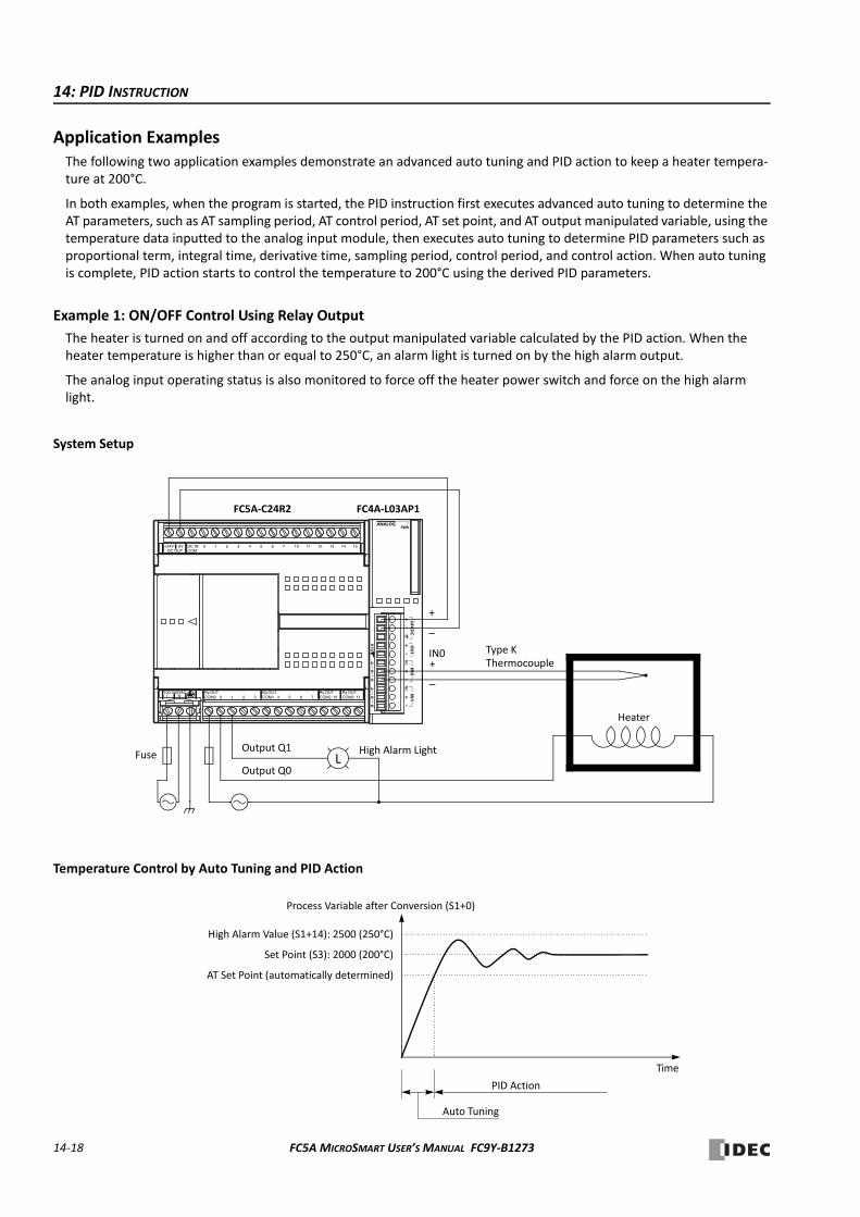
14: PID INSTRUCTION
Application ExamplesThe following two application examples demonstrate an advanced auto tuning and PID action to keep a heater tempera‐ture at 200°C.
In both examples, when the program is started, the PID instruction first executes advanced auto tuning to determine the AT parameters, such as AT sampling period, AT control period, AT set point, and AT output manipulated variable, using the temperature data inputted to the analog input module, then executes auto tuning to determine PID parameters such as proportional term, integral time, derivative time, sampling period, control period, and control action. When auto tuning is complete, PID action starts to control the temperature to 200°C using the derived PID parameters.
Example 1: ON/OFF Control Using Relay Output
The heater is turned on and off according to the output manipulated variable calculated by the PID action. When the heater temperature is higher than or equal to 250°C, an alarm light is turned on by the high alarm output.
The analog input operating status is also monitored to force off the heater power switch and force on the high alarm light.
System Setup
Temperature Control by Auto Tuning and PID Action
Type K
High Alarm LightOutput Q1
Heater
+24V 0V 10 11 12 13 14 15DC OUT COM
DC IN 0 1 2 3 4 5 6 7
L N100-240VAC Ry.OUT
COM0Ry.OUTCOM1
Ry.OUTCOM3 11
Ry.OUTCOM2 100 1 2 3 4 5 6 7
Fuse
+
–
+
–
LOutput Q0
IN0
FC5A‐C24R2 FC4A‐L03AP1
Thermocouple
Process Variable after Conversion (S1+0)
Time
High Alarm Value (S1+14): 2500 (250°C)
Set Point (S3): 2000 (200°C)
AT Set Point (automatically determined)
Auto Tuning
PID Action
14‐18 FC5A MICROSMART USER’S MANUAL FC9Y‐B1273

14: PID INSTRUCTION
Device Settings
Note: When analog I/O module FC4A‐L03AP1 is used for the PID instruction, select the binary data to make sure that the process vari‐able takes a value of 0 through 4095.
Analog Input Data vs. Process Variable after Conversion
Device Function Description Device Address (Value)
S1+3 Operation mode Advanced AT (auto tuning) + PID action D3 (3)
S1+4 Control mode Enable linear conversion, proportional band D4 (3)
S1+5 Linear conversion maximum value 1300°C D5 (13000)
S1+6 Linear conversion minimum value 0°C D6 (0)
S1+10 Integral start coefficient 100% D10 (100)
S1+11 Input filter coefficient 70% D11 (70)
S1+14 High alarm value 250°C D14 (2500)
S1+15 Low alarm value 0°C D15 (0)
S1+25 Proportional band offset value 0% D25 (0)
S1+26 Derivative gain 0% D26 (0)
S2+2Output manipulated variable limit enable
Disable output manipulated variable limits M2 (OFF)
S2+3 Integral start coefficient disable Enable integral start coefficient (S1+10) M3 (OFF)
S2+4 High alarm outputON: When temperature 250°COFF: When temperature < 250°C
M4
S2+6 Control output
Remains on during advanced auto tuning; Goes on and off according to the control period (S1+13) and output manipulated variable (S1+1) during PID action
M6
S3 Set point 200°C D100 (2000)
S4 Process variableAnalog input data of analog I/O module 1, analog input channel 0; stores 0 through 4095
D760
Analog input operating status Stores 0 through 5 D761
Analog input signal type Type K thermometer D762 (2)
Analog input data type 12‐bit data (0 to 4095) (Note) D763 (0)
D1 Manipulated variable Stores PID calculation result D50
PID start input Starts to execute the PID instruction I0
Heater power switch Turned on and off by control output M6 Q0
High alarm lightTurned on and off by high alarm output M4 and analog input error M11
Q1
Analog input errorTurns on when analog input operating status D761 is 3 or more
M11
High Alarm Value (S1+14): 2500 (250°C)
4095Linear Conversion Minimum Value (S1+6): 0 (0°C)
Linear Conversion Maximum Value (S1+5): 13000 (1300°C)
Set Point (S3): 2000 (200°C)
AT Set Point (automatically determined)
Analog Input Data D760
Process Variable after Conversion (S1+0)
Process Variable before Conversion (S4)
0
FC5A MICROSMART USER’S MANUAL FC9Y‐B1273 14‐19
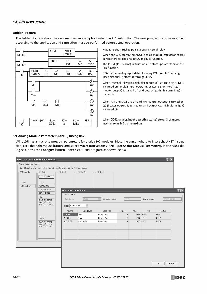
14: PID INSTRUCTION
Ladder Program
The ladder diagram shown below describes an example of using the PID instruction. The user program must be modified according to the application and simulation must be performed before actual operation.
Set Analog Module Parameters (ANST) Dialog Box
WindLDR has a macro to program parameters for analog I/O modules. Place the cursor where to insert the ANST instruc‐tion, click the right mouse button, and select Macro Instructions > ANST (Set Analog Module Parameters). In the ANST dia‐log box, press the Configure button under Slot 1, and program as shown below.
M8120
M8120 is the initialize pulse special internal relay.
When the CPU starts, the ANST (analog macro) instruction stores parameters for the analog I/O module function.
The PIDST (PID macro) instruction also stores parameters for the PID function.
D760 is the analog input data of analog I/O module 1, analog input channel 0; stores 0 through 4095
When internal relay M4 (high alarm output) is turned on or M11 is turned on (analog input operating status is 3 or more), Q0 (heater output) is turned off and output Q1 (high alarm light) is turned on.
When M4 and M11 are off and M6 (control output) is turned on, Q0 (heater output) is turned on and output Q1 (high alarm light) is turned off.
When D761 (analog input operating status) stores 3 or more, internal relay M11 is turned on.
S1D0
S2M0
PIDST S3D100
NO.1L03AP1
ANST
I0
D1D50
S1D0
S2M0
S3D100
PID(I)0‐4095
S4D760
M4
M6
Q1S
Q0
M11
REPS1 –D761
D1 –M11
CMP>=(W) S2 –3
M4 M11
Q0R
Q1R
I0
M8120
14‐20 FC5A MICROSMART USER’S MANUAL FC9Y‐B1273

14: PID INSTRUCTION
Set PID Parameters (PIDST) Dialog Box
Place the cursor where to insert the PIDST instruction, click the right mouse button, and select Macro Instructions > PIDST (Set PID Parameters). In the PIDST dialog box, program as shown below.
PID Control (PID) Dialog Box
S1+3 Operation mode S1+14 High alarm value
S1+4 Control mode S1+15 Low alarm value
S1+5 Linear conversion maximum value S1+25 Proportional band offset value
S1+6 Linear conversion minimum value S1+26 Derivative gain
S1+10 Integral start coefficient S2+2 Output manipulated variable limit enable
S1+11 Input filter coefficient S2+3 Integral start coefficient disable
S3 Set point
S1+3
S2+3
S3
S1+10
S1+4
S1+5
S1+6
S1+14
S1+11
S1+15
S2+2
S1+25
S1+26
Select options and device address as with the PID instruction.
FC5A MICROSMART USER’S MANUAL FC9Y‐B1273 14‐21

14: PID INSTRUCTION
Example 2: ON/OFF Control Using Analog Output
The output manipulated variable for analog output module (S1+24) of the PID instruction is moved to the analog output data (D772) and the analog I/O module sends out a voltage output of 0 to 10V DC. The analog output is then connected to a thyristor unit which controls the AC power using phase control.
System Setup
Temperature Control by Auto Tuning and PID Action
Device Settings for Analog I/O Module
Analog Channel
Function Description Device Address (Value)
Input Channel 0
Analog input dataAnalog input data of analog I/O module 1, analog input channel 0; stores 0 through 4095
D760
Analog input operating status Stores 0 through 5 D761
Analog input signal type Type K thermometer D762 (2)
Analog input data type 12‐bit data (0 to 4095) D763 (0)
Output
Analog output data 0 to 4095 D772
Analog output operating status Stores 0 through 4 D773
Analog output signal type Voltage output (0 to 10V DC) D774 (0)
Analog output data type 12‐bit data (0 to 4095) D775 (0)
Type K
Heater
+24V 0V 10 11 12 13 14 15DC OUT COM
DC IN 0 1 2 3 4 5 6 7
L N100-240VAC Ry.OUT
COM0Ry.OUTCOM1
Ry.OUTCOM3 11
Ry.OUTCOM2 100 1 2 3 4 5 6 7
Fuse
+
–
+
– IN0
FC5A‐C24R2 FC4A‐L03AP1
Thermocouple
1
2
L2
3
L1
Thyristor Unit
+
–
OUT
Process Variable after Conversion (S1+0)
Time
High Alarm Value (S1+14): 2500 (250°C)
Set Point (S3): 2000 (200°C)
AT Set Point (automatically determined)
Auto Tuning
PID Action
14‐22 FC5A MICROSMART USER’S MANUAL FC9Y‐B1273

14: PID INSTRUCTION
Ladder Program
The ladder diagram shown below describes an example of using the PID instruction. The user program must be modified according to the application and simulation must be performed before actual operation.
Programming in the dialog boxes of the ANST (Set Analog Module Parameters), PIDST (Set PID Parameters), and PID (PID Control) instructions are the same as the preceding example.
Notes for Using Ladder Refresh Type Analog Input Modules:
When using analog input module FC4A‐J4CN1 with Pt100 or Ni100 inputs, use the XYFS and CVXTY instructions to convert the 0‐6,000 input to 0‐50,000 input and store the result to the process variable (S4) of the PID instruction.
When using analog input module FC4A‐J4CN1 with Pt1000 or Ni1000 inputs, use the XYFS and CVXTY instructions to convert the 0‐60,000 input to 0‐50,000 input and store the result to the process variable (S4) of the PID instruction.
When using analog input module FC4A‐J8AT1, keep the operation within the temperature range where the thermistor shows linear characteristics.
When using analog input module FC4A‐J8AT1, use the XYFS and CVXTY instructions to convert the 0‐4,000 input to 0‐50,000 input and store the result to the process variable (S4) of the PID instruction.
When using analog output module FC4A‐K2C1 with voltage outputs, use the XYFS and CVXTY instructions to convert the output manipulated variable for analog output module (S1+24) and store the result to the data register designated as analog output data of the analog output module.
The following example demonstrates a program for analog input module FC4A‐J4CN1 to convert Pt1000 or Ni1000 analog input data in D410 to a value within the range between 0 and 50,000, and store the result to D510.
M8120
M8120 is the initialize pulse special internal relay.
When the CPU starts, the ANST (analog macro) instruction stores parameters for the analog I/O module function.
The PIDST (PID macro) instruction also stores parameters for the PID function.
D760 is the analog input data of analog I/O module 1, analog input channel 0; stores 0 through 4095
When internal relay M4 (high alarm output) is turned on or M11 is turned on (analog input operating status is 3 or more), 0 is set to D772 (analog output data), turning off the heater power.
When M4 and M11 are off, D24 (output manipulated variable for analog output module S1+24) of the PID instruction is moved to D772 (analog output data).
When D761 (analog input operating status) stores 3 or more, internal relay M11 is turned on.
S1D0
S2M0
PIDST S3D100
NO.1L03AP1
ANST
I0
D1D50
S1D0
S2M0
S3D100
PID(I)0‐4095
S4D760
M4
M11
REPS1 –D761
D1 –M11
CMP>=(W) S2 –3
M4 M11
I0
S1 –0
D1 –D772
MOV(W) REP
S1 –D24
D1 –D772
MOV(W) REP
M8120
M8120 is the initialize pulse special internal relay.
At startup, XYFS specifies two points.
When input I0 is on, CVXTY converts the value in D410 and stores the result to D510.
M8120
XYFS(W) Y150000
END
I0
CVXTY(W) D1D510
S11
X00
Y00
X160000
S11
S2D410
FC5A MICROSMART USER’S MANUAL FC9Y‐B1273 14‐23

14: PID INSTRUCTION
14‐24 FC5A MICROSMART USER’S MANUAL FC9Y‐B1273
15: DUAL / TEACHING TIMER INSTRUCTIONS
IntroductionDual timer instructions generate ON/OFF pulses of required durations from a designated output, internal relay, or shift register bit. Four dual timers are available and the ON/OFF duration can be selected from 1 ms up to 65535 sec.
Teaching timer instruction measures the ON duration of the start input for the teaching timer instruction and stores the measured data to a designated data register, which can be used as a preset value for a timer instruction.
DTML (1‐sec Dual Timer)
DTIM (100‐ms Dual Timer)
DTMH (10‐ms Dual Timer)
DTMS (1‐ms Dual Timer)
Applicable CPU Modules
FC5A‐C10R2/C/D FC5A‐C16R2/C/D FC5A‐C24R2/C/D FC5A‐D16RK1/RS1 FC5A‐D32K3/S3 FC5A‐D12K1E/S1E
X X X X X X
While input is on, destination device D1 repeats to turn on and off for a duration designated by devices S1 and S2, respectively.
The time range is 0 through 65535 sec.
S1*****
D1*****
DTML S2*****
D2*****
While input is on, destination device D1 repeats to turn on and off for a duration designated by devices S1 and S2, respectively.
The time range is 0 through 6553.5 sec.
S1*****
D1*****
DTIM S2*****
D2*****
While input is on, destination device D1 repeats to turn on and off for a duration designated by devices S1 and S2, respectively.
The time range is 0 through 655.35 sec.
S1*****
D1*****
DTMH S2*****
D2*****
While input is on, destination device D1 repeats to turn on and off for a duration designated by devices S1 and S2, respectively.
The time range is 0 through 65.535 sec.
S1*****
D1*****
DTMS S2*****
D2*****
FC5A MICROSMART USER’S MANUAL FC9Y‐B1273 15‐1
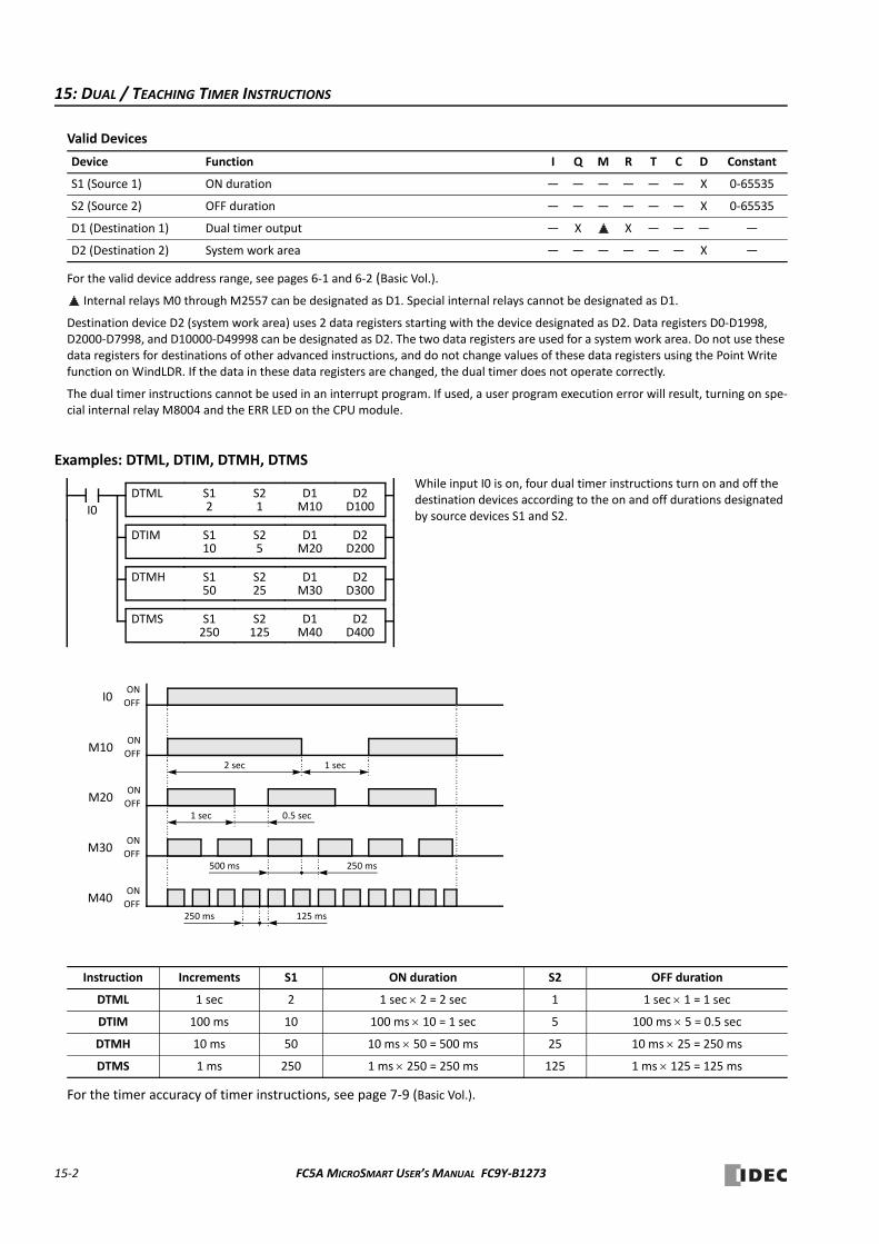
15: DUAL / TEACHING TIMER INSTRUCTIONS
Valid Devices
For the valid device address range, see pages 6‐1 and 6‐2 (Basic Vol.).
Internal relays M0 through M2557 can be designated as D1. Special internal relays cannot be designated as D1.
Destination device D2 (system work area) uses 2 data registers starting with the device designated as D2. Data registers D0‐D1998, D2000‐D7998, and D10000‐D49998 can be designated as D2. The two data registers are used for a system work area. Do not use these data registers for destinations of other advanced instructions, and do not change values of these data registers using the Point Write function on WindLDR. If the data in these data registers are changed, the dual timer does not operate correctly.
The dual timer instructions cannot be used in an interrupt program. If used, a user program execution error will result, turning on spe‐cial internal relay M8004 and the ERR LED on the CPU module.
Examples: DTML, DTIM, DTMH, DTMS
For the timer accuracy of timer instructions, see page 7‐9 (Basic Vol.).
Device Function I Q M R T C D Constant
S1 (Source 1) ON duration — — — — — — X 0‐65535
S2 (Source 2) OFF duration — — — — — — X 0‐65535
D1 (Destination 1) Dual timer output — X X — — — —
D2 (Destination 2) System work area — — — — — — X —
Instruction Increments S1 ON duration S2 OFF duration
DTML 1 sec 2 1 sec 2 = 2 sec 1 1 sec 1 = 1 sec
DTIM 100 ms 10 100 ms 10 = 1 sec 5 100 ms 5 = 0.5 sec
DTMH 10 ms 50 10 ms 50 = 500 ms 25 10 ms 25 = 250 ms
DTMS 1 ms 250 1 ms 250 = 250 ms 125 1 ms 125 = 125 ms
500 ms 250 ms
I0
D2D100
While input I0 is on, four dual timer instructions turn on and off the destination devices according to the on and off durations designated by source devices S1 and S2.
S12
D1M10
DTML S21
D2D200
S110
D1M20
DTIM S25
D2D300
S150
D1M30
DTMH S225
D2D400
S1250
D1M40
DTMS S2125
M10ON
OFF
M20ON
OFF
M30ON
OFF
I0ON
OFF
2 sec
M40ON
OFF
1 sec
1 sec 0.5 sec
250 ms 125 ms
15‐2 FC5A MICROSMART USER’S MANUAL FC9Y‐B1273
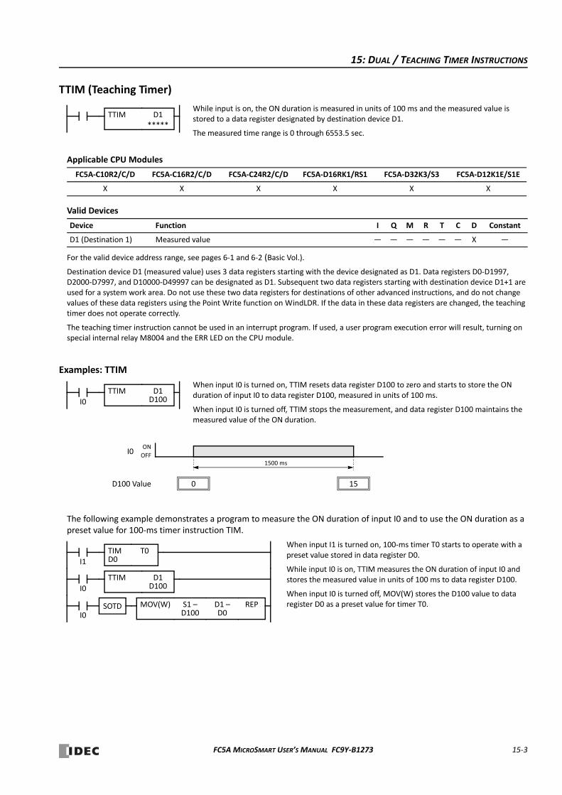
15: DUAL / TEACHING TIMER INSTRUCTIONS
TTIM (Teaching Timer)
Applicable CPU Modules
Valid Devices
For the valid device address range, see pages 6‐1 and 6‐2 (Basic Vol.).
Destination device D1 (measured value) uses 3 data registers starting with the device designated as D1. Data registers D0‐D1997, D2000‐D7997, and D10000‐D49997 can be designated as D1. Subsequent two data registers starting with destination device D1+1 are used for a system work area. Do not use these two data registers for destinations of other advanced instructions, and do not change values of these data registers using the Point Write function on WindLDR. If the data in these data registers are changed, the teaching timer does not operate correctly.
The teaching timer instruction cannot be used in an interrupt program. If used, a user program execution error will result, turning on special internal relay M8004 and the ERR LED on the CPU module.
Examples: TTIM
The following example demonstrates a program to measure the ON duration of input I0 and to use the ON duration as a preset value for 100‐ms timer instruction TIM.
FC5A‐C10R2/C/D FC5A‐C16R2/C/D FC5A‐C24R2/C/D FC5A‐D16RK1/RS1 FC5A‐D32K3/S3 FC5A‐D12K1E/S1E
X X X X X X
Device Function I Q M R T C D Constant
D1 (Destination 1) Measured value — — — — — — X —
While input is on, the ON duration is measured in units of 100 ms and the measured value is stored to a data register designated by destination device D1.
The measured time range is 0 through 6553.5 sec.
TTIM D1*****
I0
D1D100
When input I0 is turned on, TTIM resets data register D100 to zero and starts to store the ON duration of input I0 to data register D100, measured in units of 100 ms.
When input I0 is turned off, TTIM stops the measurement, and data register D100 maintains the measured value of the ON duration.
TTIM
D100 Value
I0ON
OFF1500 ms
0 15
I0
D1D100
When input I1 is turned on, 100‐ms timer T0 starts to operate with a preset value stored in data register D0.
While input I0 is on, TTIM measures the ON duration of input I0 and stores the measured value in units of 100 ms to data register D100.
When input I0 is turned off, MOV(W) stores the D100 value to data register D0 as a preset value for timer T0.
TTIM
I1
TIMD0
T0
I0SOTD REPS1 –
D100D1 –D0
MOV(W)
FC5A MICROSMART USER’S MANUAL FC9Y‐B1273 15‐3

15: DUAL / TEACHING TIMER INSTRUCTIONS
15‐4 FC5A MICROSMART USER’S MANUAL FC9Y‐B1273
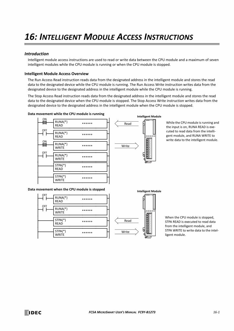
16: INTELLIGENT MODULE ACCESS INSTRUCTIONS
IntroductionIntelligent module access instructions are used to read or write data between the CPU module and a maximum of seven intelligent modules while the CPU module is running or when the CPU module is stopped.
Intelligent Module Access Overview
The Run Access Read instruction reads data from the designated address in the intelligent module and stores the read data to the designated device while the CPU module is running. The Run Access Write instruction writes data from the designated device to the designated address in the intelligent module while the CPU module is running.
The Stop Access Read instruction reads data from the designated address in the intelligent module and stores the read data to the designated device when the CPU module is stopped. The Stop Access Write instruction writes data from the designated device to the designated address in the intelligent module when the CPU module is stopped.
While the CPU module is running and the input is on, RUNA READ is exe‐cuted to read data from the intelli‐gent module, and RUNA WRITE to write data to the intelligent module.
RUNA(*)READ ******
ONRUNA(*)READ ******
OFF
RUNA(*)WRITE ******
RUNA(*)READ ******
STPA(*)READ ******
STPA(*)WRITE ******
STPA(*)READ ******
STPA(*)WRITE ******
RUNA(*)WRITE ******
ONRUNA(*)WRITE ******
OFF
OFF
OFF
Read
Write
Intelligent Module
Write
ReadWhen the CPU module is stopped, STPA READ is executed to read data from the intelligent module, and STPA WRITE to write data to the intel‐ligent module.
Intelligent ModuleData movement when the CPU module is stopped
Data movement while the CPU module is running
FC5A MICROSMART USER’S MANUAL FC9Y‐B1273 16‐1
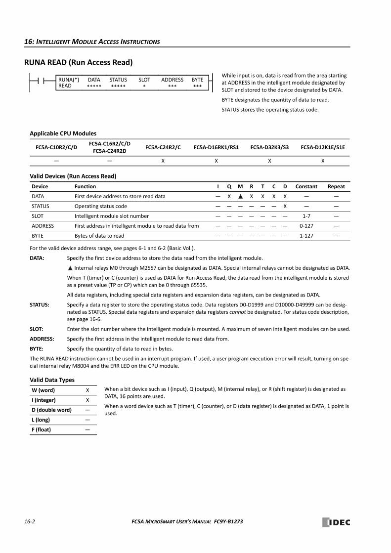
16: INTELLIGENT MODULE ACCESS INSTRUCTIONS
RUNA READ (Run Access Read)
Applicable CPU Modules
Valid Devices (Run Access Read)
For the valid device address range, see pages 6‐1 and 6‐2 (Basic Vol.).
DATA: Specify the first device address to store the data read from the intelligent module.
Internal relays M0 through M2557 can be designated as DATA. Special internal relays cannot be designated as DATA.
When T (timer) or C (counter) is used as DATA for Run Access Read, the data read from the intelligent module is stored as a preset value (TP or CP) which can be 0 through 65535.
All data registers, including special data registers and expansion data registers, can be designated as DATA.
STATUS: Specify a data register to store the operating status code. Data registers D0‐D1999 and D10000‐D49999 can be desig‐nated as STATUS. Special data registers and expansion data registers cannot be designated. For status code description, see page 16‐6.
SLOT: Enter the slot number where the intelligent module is mounted. A maximum of seven intelligent modules can be used.
ADDRESS: Specify the first address in the intelligent module to read data from.
BYTE: Specify the quantity of data to read in bytes.
The RUNA READ instruction cannot be used in an interrupt program. If used, a user program execution error will result, turning on spe‐cial internal relay M8004 and the ERR LED on the CPU module.
Valid Data Types
FC5A‐C10R2/C/DFC5A‐C16R2/C/DFC5A‐C24R2D
FC5A‐C24R2/C FC5A‐D16RK1/RS1 FC5A‐D32K3/S3 FC5A‐D12K1E/S1E
— — X X X X
Device Function I Q M R T C D Constant Repeat
DATA First device address to store read data — X X X X X — —
STATUS Operating status code — — — — — — X — —
SLOT Intelligent module slot number — — — — — — — 1‐7 —
ADDRESS First address in intelligent module to read data from — — — — — — — 0‐127 —
BYTE Bytes of data to read — — — — — — — 1‐127 —
W (word) X
I (integer) X
D (double word) —
L (long) —
F (float) —
While input is on, data is read from the area starting at ADDRESS in the intelligent module designated by SLOT and stored to the device designated by DATA.
BYTE designates the quantity of data to read.
STATUS stores the operating status code.
DATA*****
SLOT*
STATUS*****
BYTE***
ADDRESS***
RUNA(*)READ
When a bit device such as I (input), Q (output), M (internal relay), or R (shift register) is designated as DATA, 16 points are used.
When a word device such as T (timer), C (counter), or D (data register) is designated as DATA, 1 point is used.
16‐2 FC5A MICROSMART USER’S MANUAL FC9Y‐B1273
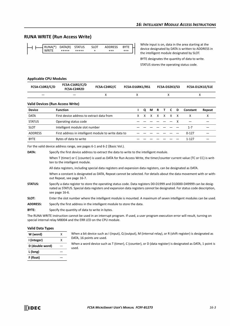
16: INTELLIGENT MODULE ACCESS INSTRUCTIONS
RUNA WRITE (Run Access Write)
Applicable CPU Modules
Valid Devices (Run Access Write)
For the valid device address range, see pages 6‐1 and 6‐2 (Basic Vol.).
DATA: Specify the first device address to extract the data to write to the intelligent module.
When T (timer) or C (counter) is used as DATA for Run Access Write, the timer/counter current value (TC or CC) is writ‐ten to the intelligent module.
All data registers, including special data registers and expansion data registers, can be designated as DATA.
When a constant is designated as DATA, Repeat cannot be selected. For details about the data movement with or with‐out Repeat, see page 16‐7.
STATUS: Specify a data register to store the operating status code. Data registers D0‐D1999 and D10000‐D49999 can be desig‐nated as STATUS. Special data registers and expansion data registers cannot be designated. For status code description, see page 16‐6.
SLOT: Enter the slot number where the intelligent module is mounted. A maximum of seven intelligent modules can be used.
ADDRESS: Specify the first address in the intelligent module to store the data.
BYTE: Specify the quantity of data to write in bytes.
The RUNA WRITE instruction cannot be used in an interrupt program. If used, a user program execution error will result, turning on special internal relay M8004 and the ERR LED on the CPU module.
Valid Data Types
FC5A‐C10R2/C/DFC5A‐C16R2/C/DFC5A‐C24R2D
FC5A‐C24R2/C FC5A‐D16RK1/RS1 FC5A‐D32K3/S3 FC5A‐D12K1E/S1E
— — X X X X
Device Function I Q M R T C D Constant Repeat
DATA First device address to extract data from X X X X X X X X X
STATUS Operating status code — — — — — — X — —
SLOT Intelligent module slot number — — — — — — — 1‐7 —
ADDRESS First address in intelligent module to write data to — — — — — — — 0‐127 —
BYTE Bytes of data to write — — — — — — — 1‐127 —
W (word) X
I (integer) X
D (double word) —
L (long) —
F (float) —
While input is on, data in the area starting at the device designated by DATA is written to ADDRESS in the intelligent module designated by SLOT.
BYTE designates the quantity of data to write.
STATUS stores the operating status code.
DATA(R)*****
SLOT*
STATUS*****
BYTE***
ADDRESS***
RUNA(*)WRITE
When a bit device such as I (input), Q (output), M (internal relay), or R (shift register) is designated as DATA, 16 points are used.
When a word device such as T (timer), C (counter), or D (data register) is designated as DATA, 1 point is used.
FC5A MICROSMART USER’S MANUAL FC9Y‐B1273 16‐3
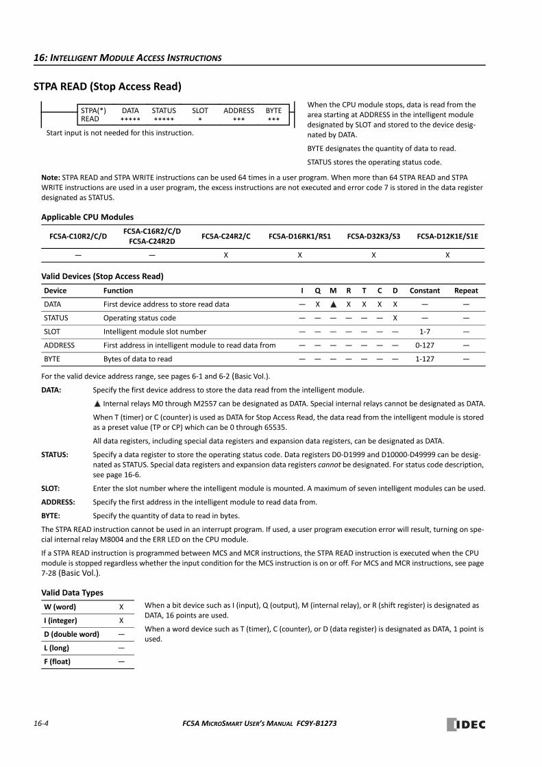
16: INTELLIGENT MODULE ACCESS INSTRUCTIONS
STPA READ (Stop Access Read)
Note: STPA READ and STPA WRITE instructions can be used 64 times in a user program. When more than 64 STPA READ and STPA WRITE instructions are used in a user program, the excess instructions are not executed and error code 7 is stored in the data register designated as STATUS.
Applicable CPU Modules
Valid Devices (Stop Access Read)
For the valid device address range, see pages 6‐1 and 6‐2 (Basic Vol.).
DATA: Specify the first device address to store the data read from the intelligent module.
Internal relays M0 through M2557 can be designated as DATA. Special internal relays cannot be designated as DATA.
When T (timer) or C (counter) is used as DATA for Stop Access Read, the data read from the intelligent module is stored as a preset value (TP or CP) which can be 0 through 65535.
All data registers, including special data registers and expansion data registers, can be designated as DATA.
STATUS: Specify a data register to store the operating status code. Data registers D0‐D1999 and D10000‐D49999 can be desig‐nated as STATUS. Special data registers and expansion data registers cannot be designated. For status code description, see page 16‐6.
SLOT: Enter the slot number where the intelligent module is mounted. A maximum of seven intelligent modules can be used.
ADDRESS: Specify the first address in the intelligent module to read data from.
BYTE: Specify the quantity of data to read in bytes.
The STPA READ instruction cannot be used in an interrupt program. If used, a user program execution error will result, turning on spe‐cial internal relay M8004 and the ERR LED on the CPU module.
If a STPA READ instruction is programmed between MCS and MCR instructions, the STPA READ instruction is executed when the CPU module is stopped regardless whether the input condition for the MCS instruction is on or off. For MCS and MCR instructions, see page 7‐28 (Basic Vol.).
Valid Data Types
FC5A‐C10R2/C/DFC5A‐C16R2/C/DFC5A‐C24R2D
FC5A‐C24R2/C FC5A‐D16RK1/RS1 FC5A‐D32K3/S3 FC5A‐D12K1E/S1E
— — X X X X
Device Function I Q M R T C D Constant Repeat
DATA First device address to store read data — X X X X X — —
STATUS Operating status code — — — — — — X — —
SLOT Intelligent module slot number — — — — — — — 1‐7 —
ADDRESS First address in intelligent module to read data from — — — — — — — 0‐127 —
BYTE Bytes of data to read — — — — — — — 1‐127 —
W (word) X
I (integer) X
D (double word) —
L (long) —
F (float) —
When the CPU module stops, data is read from the area starting at ADDRESS in the intelligent module designated by SLOT and stored to the device desig‐nated by DATA.
BYTE designates the quantity of data to read.
STATUS stores the operating status code.
DATA*****
SLOT*
STATUS*****
BYTE***
ADDRESS***
STPA(*)READ
Start input is not needed for this instruction.
When a bit device such as I (input), Q (output), M (internal relay), or R (shift register) is designated as DATA, 16 points are used.
When a word device such as T (timer), C (counter), or D (data register) is designated as DATA, 1 point is used.
16‐4 FC5A MICROSMART USER’S MANUAL FC9Y‐B1273
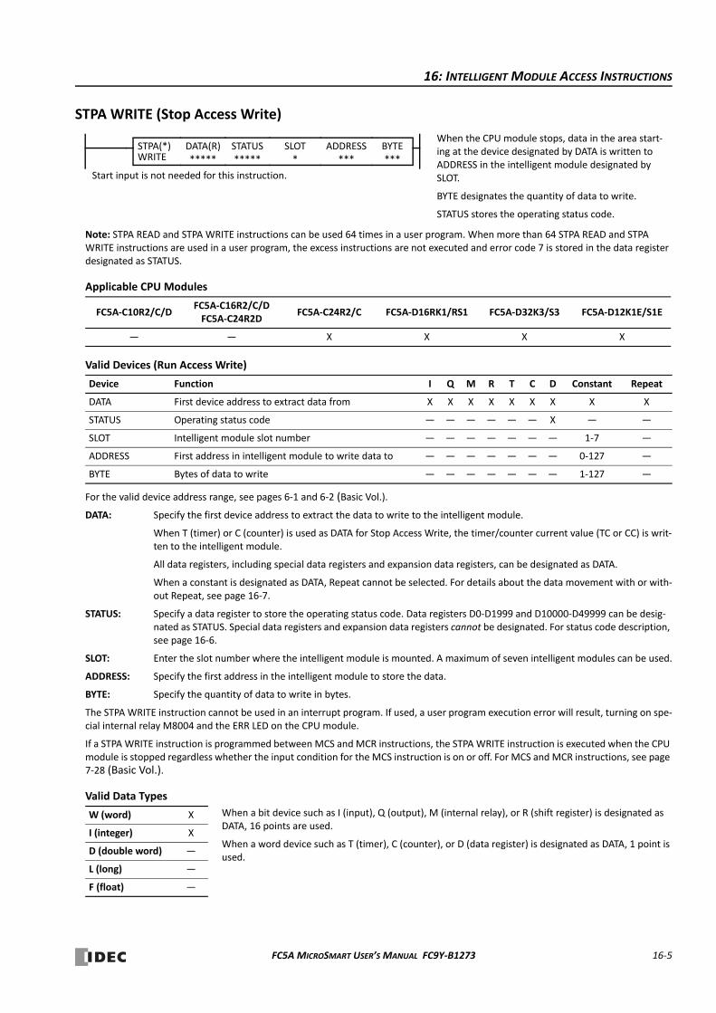
16: INTELLIGENT MODULE ACCESS INSTRUCTIONS
STPA WRITE (Stop Access Write)
Note: STPA READ and STPA WRITE instructions can be used 64 times in a user program. When more than 64 STPA READ and STPA WRITE instructions are used in a user program, the excess instructions are not executed and error code 7 is stored in the data register designated as STATUS.
Applicable CPU Modules
Valid Devices (Run Access Write)
For the valid device address range, see pages 6‐1 and 6‐2 (Basic Vol.).
DATA: Specify the first device address to extract the data to write to the intelligent module.
When T (timer) or C (counter) is used as DATA for Stop Access Write, the timer/counter current value (TC or CC) is writ‐ten to the intelligent module.
All data registers, including special data registers and expansion data registers, can be designated as DATA.
When a constant is designated as DATA, Repeat cannot be selected. For details about the data movement with or with‐out Repeat, see page 16‐7.
STATUS: Specify a data register to store the operating status code. Data registers D0‐D1999 and D10000‐D49999 can be desig‐nated as STATUS. Special data registers and expansion data registers cannot be designated. For status code description, see page 16‐6.
SLOT: Enter the slot number where the intelligent module is mounted. A maximum of seven intelligent modules can be used.
ADDRESS: Specify the first address in the intelligent module to store the data.
BYTE: Specify the quantity of data to write in bytes.
The STPA WRITE instruction cannot be used in an interrupt program. If used, a user program execution error will result, turning on spe‐cial internal relay M8004 and the ERR LED on the CPU module.
If a STPA WRITE instruction is programmed between MCS and MCR instructions, the STPA WRITE instruction is executed when the CPU module is stopped regardless whether the input condition for the MCS instruction is on or off. For MCS and MCR instructions, see page 7‐28 (Basic Vol.).
Valid Data Types
FC5A‐C10R2/C/DFC5A‐C16R2/C/DFC5A‐C24R2D
FC5A‐C24R2/C FC5A‐D16RK1/RS1 FC5A‐D32K3/S3 FC5A‐D12K1E/S1E
— — X X X X
Device Function I Q M R T C D Constant Repeat
DATA First device address to extract data from X X X X X X X X X
STATUS Operating status code — — — — — — X — —
SLOT Intelligent module slot number — — — — — — — 1‐7 —
ADDRESS First address in intelligent module to write data to — — — — — — — 0‐127 —
BYTE Bytes of data to write — — — — — — — 1‐127 —
W (word) X
I (integer) X
D (double word) —
L (long) —
F (float) —
When the CPU module stops, data in the area start‐ing at the device designated by DATA is written to ADDRESS in the intelligent module designated by SLOT.
BYTE designates the quantity of data to write.
STATUS stores the operating status code.
DATA(R)*****
SLOT*
STATUS*****
BYTE***
ADDRESS***
STPA(*)WRITE
Start input is not needed for this instruction.
When a bit device such as I (input), Q (output), M (internal relay), or R (shift register) is designated as DATA, 16 points are used.
When a word device such as T (timer), C (counter), or D (data register) is designated as DATA, 1 point is used.
FC5A MICROSMART USER’S MANUAL FC9Y‐B1273 16‐5
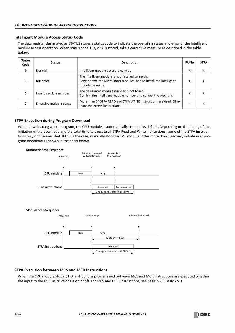
16: INTELLIGENT MODULE ACCESS INSTRUCTIONS
Intelligent Module Access Status Code
The data register designated as STATUS stores a status code to indicate the operating status and error of the intelligent module access operation. When status code 1, 3, or 7 is stored, take a corrective measure as described in the table below:
STPA Execution during Program Download
When downloading a user program, the CPU module is automatically stopped as default. Depending on the timing of the initiation of the download and the total time to execute all STPA Read and Write instructions, some of the STPA instruc‐tions may not be executed. If this is the case, manually stop the CPU module. After more than 1 second, initiate user pro‐gram download as shown in the chart below.
STPA Execution between MCS and MCR Instructions
When the CPU module stops, STPA instructions programmed between MCS and MCR instructions are executed whether the input to the MCS instructions is on or off. For MCS and MCR instructions, see page 7‐28 (Basic Vol.).
Status Code
Status Description RUNA STPA
0 Normal Intelligent module access is normal. X X
1 Bus errorThe intelligent module is not installed correctly.Power down the MicroSmart modules, and re‐install the intelligent module correctly.
X X
3 Invalid module numberThe designated module number is not found.Confirm the intelligent module number and correct the program.
X X
7 Excessive multiple usageMore than 64 STPA READ and STPA WRITE instructions are used. Elim‐inate the excess instructions.
— X
STPA instructions
CPU module
One cycle to execute all STPAs
Run
Power up
Stop
Initiate downloadAutomatic stop
Executed Not executed
Actual start to download
STPA instructions
CPU module
One cycle to execute all STPAs
Run
Power up
Stop
Manual stop
Executed
Initiate download
More than 1 sec
Automatic Stop Sequence
Manual Stop Sequence
16‐6 FC5A MICROSMART USER’S MANUAL FC9Y‐B1273
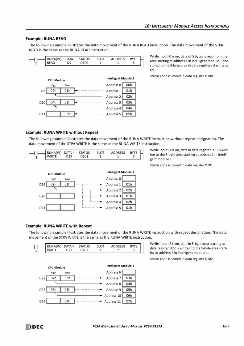
16: INTELLIGENT MODULE ACCESS INSTRUCTIONS
Example: RUNA READ
The following example illustrates the data movement of the RUNA READ instruction. The data movement of the STPA READ is the same as the RUNA READ instruction.
Example: RUNA WRITE without Repeat
The following example illustrates the data movement of the RUNA WRITE instruction without repeat designation. The data movement of the STPA WRITE is the same as the RUNA WRITE instruction.
Example: RUNA WRITE with Repeat
The following example illustrates the data movement of the RUNA WRITE instruction with repeat designation. The data movement of the STPA WRITE is the same as the RUNA WRITE instruction.
While input I0 is on, data of 5 bytes is read from the area starting at address 1 in intelligent module 1 and stored to the 5‐byte area in data registers starting at D9.
Status code is stored in data register D100.
I0
DATAD9
SLOT1
STATUSD100
BYTE5
ADDRESS1READ
RUNA(W)
02hD9
04hD10
D11
High
01h
Low
03h
05h
00hAddress 0
01hAddress 1
02hAddress 2
03hAddress 3
04hAddress 4
05hAddress 5
CPU ModuleIntelligent Module 1
While input I1 is on, data in data register D19 is writ‐ten to the 5‐byte area starting at address 1 in intelli‐gent module 1.
Status code is stored in data register D101.
I1
DATA –D19
SLOT1
STATUSD101
BYTE5
ADDRESS1WRITE
RUNA(W)
02hD19
D20
D21
High
01h
Low Address 0
01hAddress 1
02hAddress 2
01hAddress 3
02hAddress 4
01hAddress 5
CPU ModuleIntelligent Module 1
While input I2 is on, data in 5‐byte area starting at data register D22 is written to the 5‐byte area start‐ing at address 7 in intelligent module 1.
Status code is stored in data register D102.
I2
DATA RD22
SLOT1
STATUSD102
BYTE5
ADDRESS7WRITE
RUNA(W)
04hD22
06hD23
D24
High
03h
Low
05h
07h
Address 6
03hAddress 7
04hAddress 8
05hAddress 9
06hAddress 10
07hAddress 11
CPU ModuleIntelligent Module 1
FC5A MICROSMART USER’S MANUAL FC9Y‐B1273 16‐7

16: INTELLIGENT MODULE ACCESS INSTRUCTIONS
16‐8 FC5A MICROSMART USER’S MANUAL FC9Y‐B1273
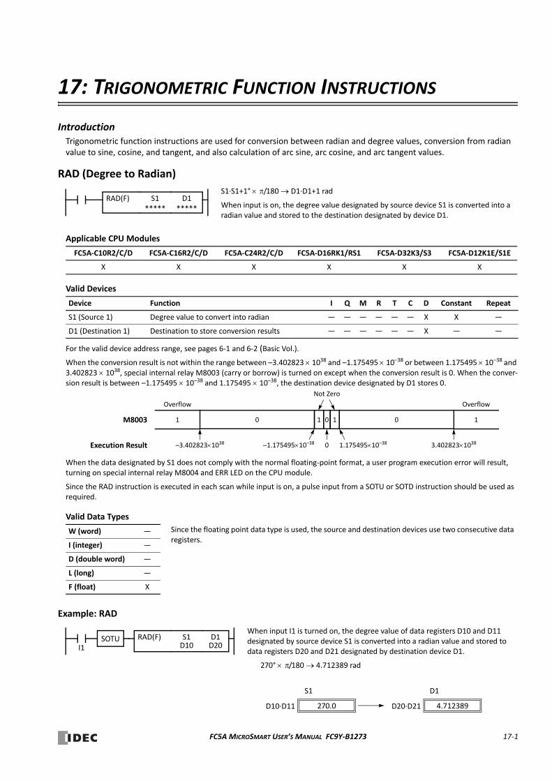
17: TRIGONOMETRIC FUNCTION INSTRUCTIONS
IntroductionTrigonometric function instructions are used for conversion between radian and degree values, conversion from radian value to sine, cosine, and tangent, and also calculation of arc sine, arc cosine, and arc tangent values.
RAD (Degree to Radian)
Applicable CPU Modules
Valid Devices
For the valid device address range, see pages 6‐1 and 6‐2 (Basic Vol.).
When the conversion result is not within the range between –3.402823 1038 and –1.175495 10–38 or between 1.175495 10–38 and 3.402823 1038, special internal relay M8003 (carry or borrow) is turned on except when the conversion result is 0. When the conver‐sion result is between –1.175495 10–38 and 1.175495 10–38, the destination device designated by D1 stores 0.
When the data designated by S1 does not comply with the normal floating‐point format, a user program execution error will result, turning on special internal relay M8004 and ERR LED on the CPU module.
Since the RAD instruction is executed in each scan while input is on, a pulse input from a SOTU or SOTD instruction should be used as required.
Valid Data Types
Example: RAD
FC5A‐C10R2/C/D FC5A‐C16R2/C/D FC5A‐C24R2/C/D FC5A‐D16RK1/RS1 FC5A‐D32K3/S3 FC5A‐D12K1E/S1E
X X X X X X
Device Function I Q M R T C D Constant Repeat
S1 (Source 1) Degree value to convert into radian — — — — — — X X —
D1 (Destination 1) Destination to store conversion results — — — — — — X — —
W (word) —
I (integer) —
D (double word) —
L (long) —
F (float) X
S1∙S1+1° /180 D1∙D1+1 rad
When input is on, the degree value designated by source device S1 is converted into a radian value and stored to the destination designated by device D1.
RAD(F) S1
*****D1
*****
0
–1.17549510–38
M8003 1 1
1.17549510–380–3.4028231038
0
Execution Result
1
Overflow
0 1
3.4028231038
Overflow
Not Zero
Since the floating point data type is used, the source and destination devices use two consecutive data registers.
I1
S1D10
RAD(F) D1D20
When input I1 is turned on, the degree value of data registers D10 and D11 designated by source device S1 is converted into a radian value and stored to data registers D20 and D21 designated by destination device D1.
270° /180 4.712389 rad
D1S1
270.0D10∙D11 4.712389D20∙D21
SOTU
FC5A MICROSMART USER’S MANUAL FC9Y‐B1273 17‐1

17: TRIGONOMETRIC FUNCTION INSTRUCTIONS
DEG (Radian to Degree)
Applicable CPU Modules
Valid Devices
For the valid device address range, see pages 6‐1 and 6‐2 (Basic Vol.).
When the conversion result is not within the range between –3.402823 1038 and –1.175495 10–38 or between 1.175495 10–38 and 3.402823 1038, special internal relay M8003 (carry or borrow) is turned on except when the conversion result is 0. When the conver‐sion result is below –3.402823 1038 or over 3.402823 1038, causing an overflow, the destination device designated by D1 stores a value of minus or plus infinity.
When the data designated by S1 does not comply with the normal floating‐point format, a user program execution error will result, turning on special internal relay M8004 and ERR LED on the CPU module.
Since the DEG instruction is executed in each scan while input is on, a pulse input from a SOTU or SOTD instruction should be used as required.
Valid Data Types
Example: DEG
FC5A‐C10R2/C/D FC5A‐C16R2/C/D FC5A‐C24R2/C/D FC5A‐D16RK1/RS1 FC5A‐D32K3/S3 FC5A‐D12K1E/S1E
X X X X X X
Device Function I Q M R T C D Constant Repeat
S1 (Source 1) Radian value to convert into degree — — — — — — X X —
D1 (Destination 1) Destination to store conversion results — — — — — — X — —
W (word) —
I (integer) —
D (double word) —
L (long) —
F (float) X
S1∙S1+1 rad 180/ D1∙D1+1°
When input is on, the radian value designated by source device S1 is converted into a degree value and stored to the destination designated by device D1.
DEG(F) S1
*****D1
*****
0
–1.17549510–38
M8003 1 1
1.17549510–380–3.4028231038
0
Execution Result
1
Overflow
0 1
3.4028231038
Overflow
Not Zero
Since the floating point data type is used, the source and destination devices use two consecutive data registers.
I1
S1D10
DEG(F) D1D20
When input I1 is turned on, the radian value of data registers D10 and D11 des‐ignated by source device S1 is converted into a degree value and stored to data registers D20 and D21 designated by destination device D1.
4.712389 rad 180/ 270.0°
D1S1
4.712389D10∙D11 270.0D20∙D21
SOTU
17‐2 FC5A MICROSMART USER’S MANUAL FC9Y‐B1273
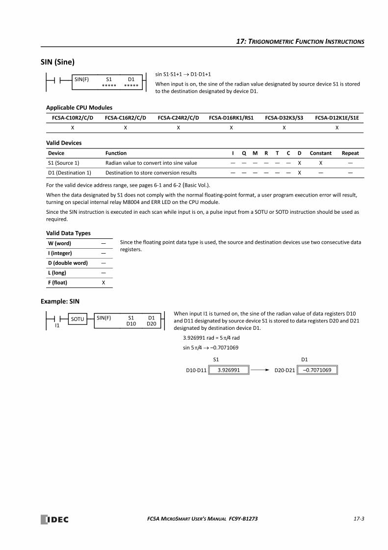
17: TRIGONOMETRIC FUNCTION INSTRUCTIONS
SIN (Sine)
Applicable CPU Modules
Valid Devices
For the valid device address range, see pages 6‐1 and 6‐2 (Basic Vol.).
When the data designated by S1 does not comply with the normal floating‐point format, a user program execution error will result, turning on special internal relay M8004 and ERR LED on the CPU module.
Since the SIN instruction is executed in each scan while input is on, a pulse input from a SOTU or SOTD instruction should be used as required.
Valid Data Types
Example: SIN
FC5A‐C10R2/C/D FC5A‐C16R2/C/D FC5A‐C24R2/C/D FC5A‐D16RK1/RS1 FC5A‐D32K3/S3 FC5A‐D12K1E/S1E
X X X X X X
Device Function I Q M R T C D Constant Repeat
S1 (Source 1) Radian value to convert into sine value — — — — — — X X —
D1 (Destination 1) Destination to store conversion results — — — — — — X — —
W (word) —
I (integer) —
D (double word) —
L (long) —
F (float) X
sin S1∙S1+1 D1∙D1+1
When input is on, the sine of the radian value designated by source device S1 is stored to the destination designated by device D1.
SIN(F) S1*****
D1*****
Since the floating point data type is used, the source and destination devices use two consecutive data registers.
I1
S1D10
SIN(F) D1D20
When input I1 is turned on, the sine of the radian value of data registers D10 and D11 designated by source device S1 is stored to data registers D20 and D21 designated by destination device D1.
3.926991 rad = 5 /4 rad
sin 5 /4 –0.7071069
D1S1
3.926991D10∙D11 –0.7071069D20∙D21
SOTU
FC5A MICROSMART USER’S MANUAL FC9Y‐B1273 17‐3

17: TRIGONOMETRIC FUNCTION INSTRUCTIONS
COS (Cosine)
Applicable CPU Modules
Valid Devices
For the valid device address range, see pages 6‐1 and 6‐2 (Basic Vol.).
When the data designated by S1 does not comply with the normal floating‐point format, a user program execution error will result, turning on special internal relay M8004 and ERR LED on the CPU module.
Since the COS instruction is executed in each scan while input is on, a pulse input from a SOTU or SOTD instruction should be used as required.
Valid Data Types
Example: COS
FC5A‐C10R2/C/D FC5A‐C16R2/C/D FC5A‐C24R2/C/D FC5A‐D16RK1/RS1 FC5A‐D32K3/S3 FC5A‐D12K1E/S1E
X X X X X X
Device Function I Q M R T C D Constant Repeat
S1 (Source 1) Radian value to convert into cosine value — — — — — — X X —
D1 (Destination 1) Destination to store conversion results — — — — — — X — —
W (word) —
I (integer) —
D (double word) —
L (long) —
F (float) X
cos S1∙S1+1 D1∙D1+1
When input is on, the cosine of the radian value designated by source device S1 is stored to the destination designated by device D1.
COS(F) S1*****
D1*****
Since the floating point data type is used, the source and destination devices use two consecutive data registers.
I1
S1D10
COS(F) D1D20
When input I1 is turned on, the cosine of the radian value of data registers D10 and D11 designated by source device S1 is stored to data registers D20 and D21 designated by destination device D1.
3.926991 rad = 5 /4 rad
cos 5 /4 –0.7071068
D1S1
3.926991D10∙D11 –0.7071068D20∙D21
SOTU
17‐4 FC5A MICROSMART USER’S MANUAL FC9Y‐B1273
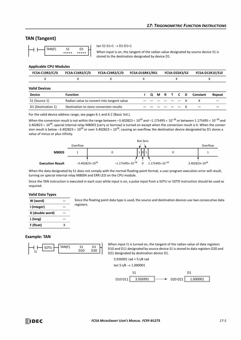
17: TRIGONOMETRIC FUNCTION INSTRUCTIONS
TAN (Tangent)
Applicable CPU Modules
Valid Devices
For the valid device address range, see pages 6‐1 and 6‐2 (Basic Vol.).
When the conversion result is not within the range between –3.402823 1038 and –1.175495 10–38 or between 1.175495 10–38 and 3.402823 1038, special internal relay M8003 (carry or borrow) is turned on except when the conversion result is 0. When the conver‐sion result is below –3.402823 1038 or over 3.402823 1038, causing an overflow, the destination device designated by D1 stores a value of minus or plus infinity.
When the data designated by S1 does not comply with the normal floating‐point format, a user program execution error will result, turning on special internal relay M8004 and ERR LED on the CPU module.
Since the TAN instruction is executed in each scan while input is on, a pulse input from a SOTU or SOTD instruction should be used as required.
Valid Data Types
Example: TAN
FC5A‐C10R2/C/D FC5A‐C16R2/C/D FC5A‐C24R2/C/D FC5A‐D16RK1/RS1 FC5A‐D32K3/S3 FC5A‐D12K1E/S1E
X X X X X X
Device Function I Q M R T C D Constant Repeat
S1 (Source 1) Radian value to convert into tangent value — — — — — — X X —
D1 (Destination 1) Destination to store conversion results — — — — — — X — —
W (word) —
I (integer) —
D (double word) —
L (long) —
F (float) X
tan S1∙S1+1 D1∙D1+1
When input is on, the tangent of the radian value designated by source device S1 is stored to the destination designated by device D1.
TAN(F) S1*****
D1*****
0
–1.17549510–38
M8003 1 1
1.17549510–380–3.4028231038
0
Execution Result
1
Overflow
0 1
3.4028231038
Overflow
Not Zero
Since the floating point data type is used, the source and destination devices use two consecutive data registers.
I1
S1D10
TAN(F) D1D20
When input I1 is turned on, the tangent of the radian value of data registers D10 and D11 designated by source device S1 is stored to data registers D20 and D21 designated by destination device D1.
3.926991 rad = 5 /4 rad
tan 5 /4 1.000001
D1S1
3.926991D10∙D11 1.000001D20∙D21
SOTU
FC5A MICROSMART USER’S MANUAL FC9Y‐B1273 17‐5
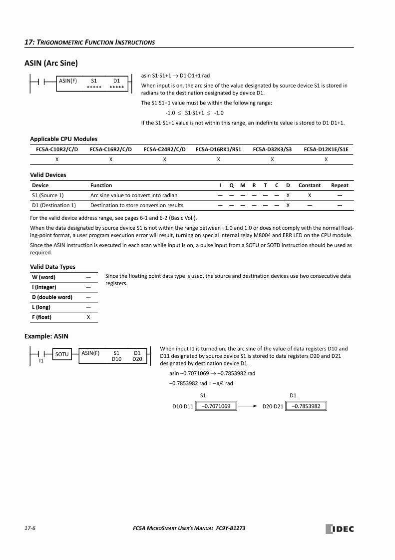
17: TRIGONOMETRIC FUNCTION INSTRUCTIONS
ASIN (Arc Sine)
Applicable CPU Modules
Valid Devices
For the valid device address range, see pages 6‐1 and 6‐2 (Basic Vol.).
When the data designated by source device S1 is not within the range between –1.0 and 1.0 or does not comply with the normal float‐ing‐point format, a user program execution error will result, turning on special internal relay M8004 and ERR LED on the CPU module.
Since the ASIN instruction is executed in each scan while input is on, a pulse input from a SOTU or SOTD instruction should be used as required.
Valid Data Types
Example: ASIN
FC5A‐C10R2/C/D FC5A‐C16R2/C/D FC5A‐C24R2/C/D FC5A‐D16RK1/RS1 FC5A‐D32K3/S3 FC5A‐D12K1E/S1E
X X X X X X
Device Function I Q M R T C D Constant Repeat
S1 (Source 1) Arc sine value to convert into radian — — — — — — X X —
D1 (Destination 1) Destination to store conversion results — — — — — — X — —
W (word) —
I (integer) —
D (double word) —
L (long) —
F (float) X
asin S1∙S1+1 D1∙D1+1 rad
When input is on, the arc sine of the value designated by source device S1 is stored in radians to the destination designated by device D1.
The S1∙S1+1 value must be within the following range:
‐1.0 S1∙S1+1 ‐1.0
If the S1∙S1+1 value is not within this range, an indefinite value is stored to D1∙D1+1.
ASIN(F) S1*****
D1*****
Since the floating point data type is used, the source and destination devices use two consecutive data registers.
I1
S1D10
ASIN(F) D1D20
When input I1 is turned on, the arc sine of the value of data registers D10 and D11 designated by source device S1 is stored to data registers D20 and D21 designated by destination device D1.
asin –0.7071069 –0.7853982 rad
–0.7853982 rad = – /4 rad
D1S1
–0.7071069D10∙D11 –0.7853982D20∙D21
SOTU
17‐6 FC5A MICROSMART USER’S MANUAL FC9Y‐B1273
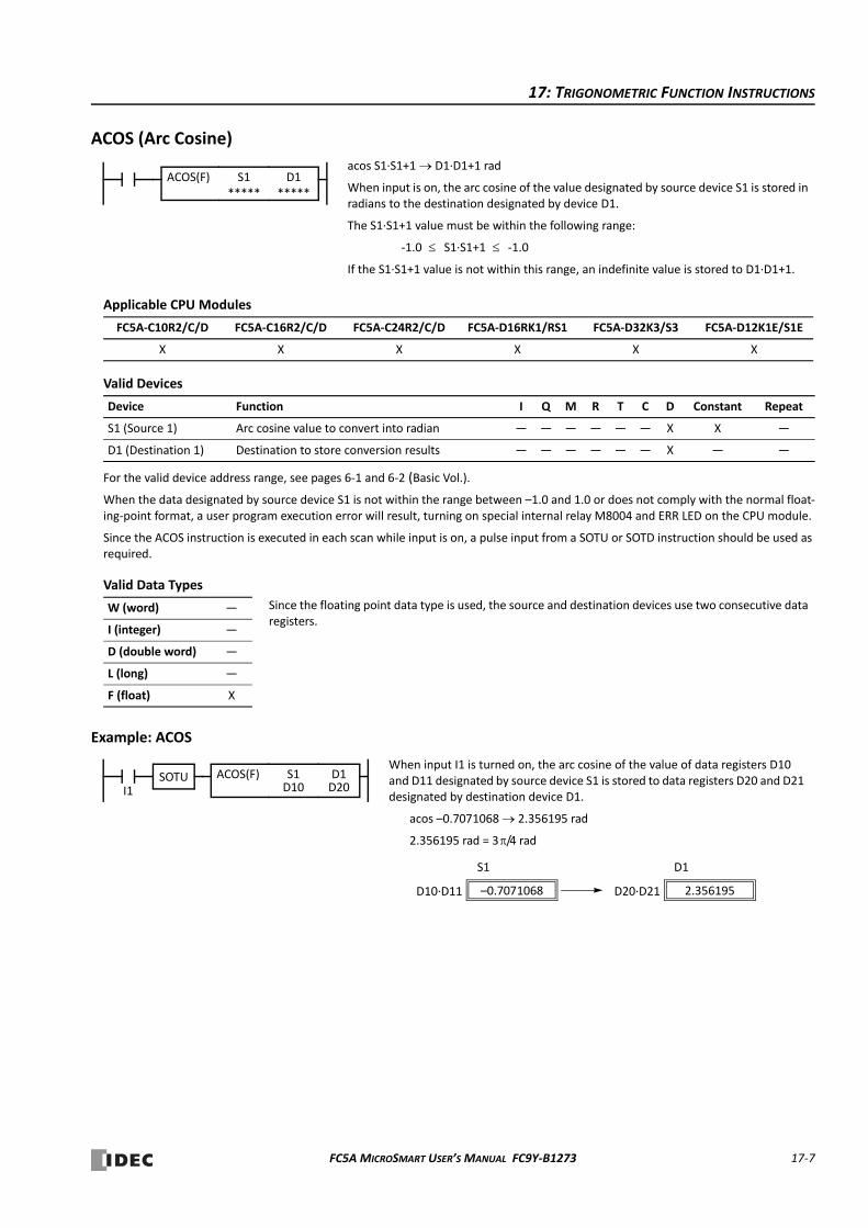
17: TRIGONOMETRIC FUNCTION INSTRUCTIONS
ACOS (Arc Cosine)
Applicable CPU Modules
Valid Devices
For the valid device address range, see pages 6‐1 and 6‐2 (Basic Vol.).
When the data designated by source device S1 is not within the range between –1.0 and 1.0 or does not comply with the normal float‐ing‐point format, a user program execution error will result, turning on special internal relay M8004 and ERR LED on the CPU module.
Since the ACOS instruction is executed in each scan while input is on, a pulse input from a SOTU or SOTD instruction should be used as required.
Valid Data Types
Example: ACOS
FC5A‐C10R2/C/D FC5A‐C16R2/C/D FC5A‐C24R2/C/D FC5A‐D16RK1/RS1 FC5A‐D32K3/S3 FC5A‐D12K1E/S1E
X X X X X X
Device Function I Q M R T C D Constant Repeat
S1 (Source 1) Arc cosine value to convert into radian — — — — — — X X —
D1 (Destination 1) Destination to store conversion results — — — — — — X — —
W (word) —
I (integer) —
D (double word) —
L (long) —
F (float) X
acos S1∙S1+1 D1∙D1+1 rad
When input is on, the arc cosine of the value designated by source device S1 is stored in radians to the destination designated by device D1.
The S1∙S1+1 value must be within the following range:
‐1.0 S1∙S1+1 ‐1.0
If the S1∙S1+1 value is not within this range, an indefinite value is stored to D1∙D1+1.
ACOS(F) S1*****
D1*****
Since the floating point data type is used, the source and destination devices use two consecutive data registers.
I1
S1D10
ACOS(F) D1D20
When input I1 is turned on, the arc cosine of the value of data registers D10 and D11 designated by source device S1 is stored to data registers D20 and D21 designated by destination device D1.
acos –0.7071068 2.356195 rad
2.356195 rad = 3 /4 rad
D1S1
–0.7071068D10∙D11 2.356195D20∙D21
SOTU
FC5A MICROSMART USER’S MANUAL FC9Y‐B1273 17‐7
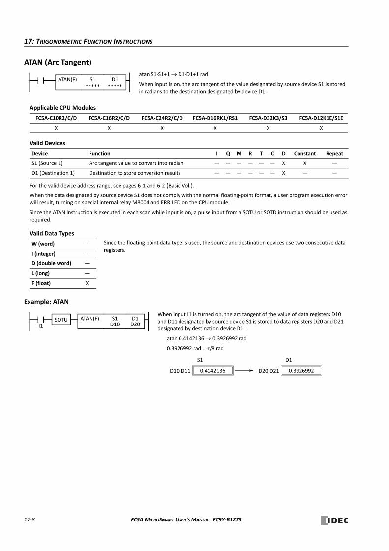
17: TRIGONOMETRIC FUNCTION INSTRUCTIONS
ATAN (Arc Tangent)
Applicable CPU Modules
Valid Devices
For the valid device address range, see pages 6‐1 and 6‐2 (Basic Vol.).
When the data designated by source device S1 does not comply with the normal floating‐point format, a user program execution error will result, turning on special internal relay M8004 and ERR LED on the CPU module.
Since the ATAN instruction is executed in each scan while input is on, a pulse input from a SOTU or SOTD instruction should be used as required.
Valid Data Types
Example: ATAN
FC5A‐C10R2/C/D FC5A‐C16R2/C/D FC5A‐C24R2/C/D FC5A‐D16RK1/RS1 FC5A‐D32K3/S3 FC5A‐D12K1E/S1E
X X X X X X
Device Function I Q M R T C D Constant Repeat
S1 (Source 1) Arc tangent value to convert into radian — — — — — — X X —
D1 (Destination 1) Destination to store conversion results — — — — — — X — —
W (word) —
I (integer) —
D (double word) —
L (long) —
F (float) X
atan S1∙S1+1 D1∙D1+1 rad
When input is on, the arc tangent of the value designated by source device S1 is stored in radians to the destination designated by device D1.
ATAN(F) S1*****
D1*****
Since the floating point data type is used, the source and destination devices use two consecutive data registers.
I1
S1D10
ATAN(F) D1D20
When input I1 is turned on, the arc tangent of the value of data registers D10 and D11 designated by source device S1 is stored to data registers D20 and D21 designated by destination device D1.
atan 0.4142136 0.3926992 rad
0.3926992 rad = /8 rad
D1S1
0.4142136D10∙D11 0.3926992D20∙D21
SOTU
17‐8 FC5A MICROSMART USER’S MANUAL FC9Y‐B1273

18: LOGARITHM / POWER INSTRUCTIONS
IntroductionThis chapter describes logarithm and power instructions which are used to calculate logarithm or powered values of source devices.
LOGE (Natural Logarithm)
Applicable CPU Modules
Valid Devices
For the valid device address range, see pages 6‐1 and 6‐2 (Basic Vol.).
When the data designated by source device S1 is less than or equal to 0 or does not comply with the normal floating‐point format, a user program execution error will result, turning on special internal relay M8004 and ERR LED on the CPU module.
Since the LOGE instruction is executed in each scan while input is on, a pulse input from a SOTU or SOTD instruction should be used as required.
Valid Data Types
Example: LOGE
FC5A‐C10R2/C/D FC5A‐C16R2/C/D FC5A‐C24R2/C/D FC5A‐D16RK1/RS1 FC5A‐D32K3/S3 FC5A‐D12K1E/S1E
X X X X X X
Device Function I Q M R T C D Constant Repeat
S1 (Source 1) Binary data to convert into natural logarithm — — — — — — X X —
D1 (Destination 1) Destination to store conversion results — — — — — — X — —
W (word) —
I (integer) —
D (double word) —
L (long) —
F (float) X
loge S1∙S1+1 D1∙D1+1
When input is on, the natural logarithm of the binary data designated by source device S1 is stored to the destination designated by device D1.
LOGE(F) S1*****
D1*****
Since the floating point data type is used, the source and destination devices use two consecutive data registers.
I1
S1D10
LOGE(F) D1D20
When input I1 is on, the natural logarithm of the binary data of data registers D10 and D11 designated by source device S1 is stored to data registers D20 and D21 designated by destination device D1.
loge 86 4.454347
D1S1
86.0D10∙D11 4.454347D20∙D21
SOTU
FC5A MICROSMART USER’S MANUAL FC9Y‐B1273 18‐1
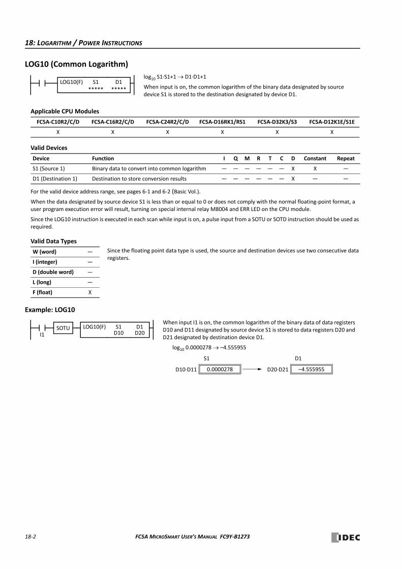
18: LOGARITHM / POWER INSTRUCTIONS
LOG10 (Common Logarithm)
Applicable CPU Modules
Valid Devices
For the valid device address range, see pages 6‐1 and 6‐2 (Basic Vol.).
When the data designated by source device S1 is less than or equal to 0 or does not comply with the normal floating‐point format, a user program execution error will result, turning on special internal relay M8004 and ERR LED on the CPU module.
Since the LOG10 instruction is executed in each scan while input is on, a pulse input from a SOTU or SOTD instruction should be used as required.
Valid Data Types
Example: LOG10
FC5A‐C10R2/C/D FC5A‐C16R2/C/D FC5A‐C24R2/C/D FC5A‐D16RK1/RS1 FC5A‐D32K3/S3 FC5A‐D12K1E/S1E
X X X X X X
Device Function I Q M R T C D Constant Repeat
S1 (Source 1) Binary data to convert into common logarithm — — — — — — X X —
D1 (Destination 1) Destination to store conversion results — — — — — — X — —
W (word) —
I (integer) —
D (double word) —
L (long) —
F (float) X
log10 S1∙S1+1 D1∙D1+1
When input is on, the common logarithm of the binary data designated by source device S1 is stored to the destination designated by device D1.
LOG10(F) S1*****
D1*****
Since the floating point data type is used, the source and destination devices use two consecutive data registers.
I1
S1D10
LOG10(F) D1D20
When input I1 is on, the common logarithm of the binary data of data registers D10 and D11 designated by source device S1 is stored to data registers D20 and D21 designated by destination device D1.
log10 0.0000278 –4.555955
D1S1
0.0000278D10∙D11 –4.555955D20∙D21
SOTU
18‐2 FC5A MICROSMART USER’S MANUAL FC9Y‐B1273
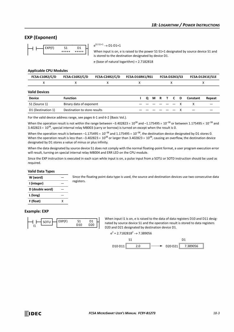
18: LOGARITHM / POWER INSTRUCTIONS
EXP (Exponent)
Applicable CPU Modules
Valid Devices
For the valid device address range, see pages 6‐1 and 6‐2 (Basic Vol.).
When the operation result is not within the range between –3.402823 1038 and –1.175495 10–38 or between 1.175495 10–38 and 3.402823 1038, special internal relay M8003 (carry or borrow) is turned on except when the result is 0.
When the operation result is between –1.175495 10–38 and 1.175495 10–38, the destination device designated by D1 stores 0. When the operation result is less than –3.402823 1038 or larger than 3.402823 1038, causing an overflow, the destination device designated by D1 stores a value of minus or plus infinity.
When the data designated by source device S1 does not comply with the normal floating‐point format, a user program execution error will result, turning on special internal relay M8004 and ERR LED on the CPU module.
Since the EXP instruction is executed in each scan while input is on, a pulse input from a SOTU or SOTD instruction should be used as required.
Valid Data Types
Example: EXP
FC5A‐C10R2/C/D FC5A‐C16R2/C/D FC5A‐C24R2/C/D FC5A‐D16RK1/RS1 FC5A‐D32K3/S3 FC5A‐D12K1E/S1E
X X X X X X
Device Function I Q M R T C D Constant Repeat
S1 (Source 1) Binary data of exponent — — — — — — X X —
D1 (Destination 1) Destination to store results — — — — — — X — —
W (word) —
I (integer) —
D (double word) —
L (long) —
F (float) X
eS1∙S1+1 D1∙D1+1
When input is on, e is raised to the power S1∙S1+1 designated by source device S1 and is stored to the destination designated by device D1.
e (base of natural logarithm) = 2.7182818
EXP(F) S1*****
D1*****
Since the floating point data type is used, the source and destination devices use two consecutive data registers.
I1
S1D10
EXP(F) D1D20
When input I1 is on, e is raised to the data of data registers D10 and D11 desig‐nated by source device S1 and the operation result is stored to data registers D20 and D21 designated by destination device D1.
e2 = 2.71828182 7.389056
D1S1
2.0D10∙D11 7.389056D20∙D21
SOTU
FC5A MICROSMART USER’S MANUAL FC9Y‐B1273 18‐3
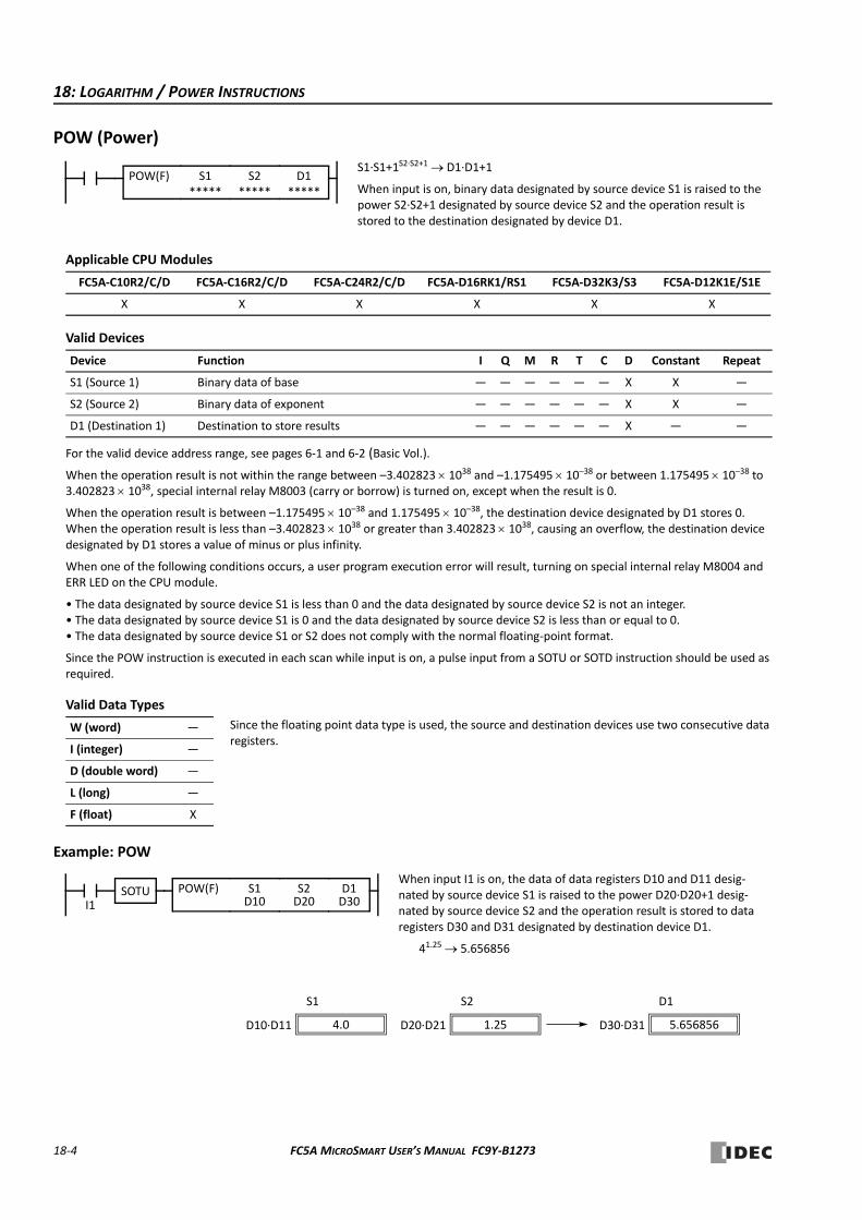
18: LOGARITHM / POWER INSTRUCTIONS
POW (Power)
Applicable CPU Modules
Valid Devices
For the valid device address range, see pages 6‐1 and 6‐2 (Basic Vol.).
When the operation result is not within the range between –3.402823 1038 and –1.175495 10–38 or between 1.175495 10–38 to 3.402823 1038, special internal relay M8003 (carry or borrow) is turned on, except when the result is 0.
When the operation result is between –1.175495 10–38 and 1.175495 10–38, the destination device designated by D1 stores 0. When the operation result is less than –3.402823 1038 or greater than 3.402823 1038, causing an overflow, the destination device designated by D1 stores a value of minus or plus infinity.
When one of the following conditions occurs, a user program execution error will result, turning on special internal relay M8004 and ERR LED on the CPU module.
• The data designated by source device S1 is less than 0 and the data designated by source device S2 is not an integer.• The data designated by source device S1 is 0 and the data designated by source device S2 is less than or equal to 0.• The data designated by source device S1 or S2 does not comply with the normal floating‐point format.
Since the POW instruction is executed in each scan while input is on, a pulse input from a SOTU or SOTD instruction should be used as required.
Valid Data Types
Example: POW
FC5A‐C10R2/C/D FC5A‐C16R2/C/D FC5A‐C24R2/C/D FC5A‐D16RK1/RS1 FC5A‐D32K3/S3 FC5A‐D12K1E/S1E
X X X X X X
Device Function I Q M R T C D Constant Repeat
S1 (Source 1) Binary data of base — — — — — — X X —
S2 (Source 2) Binary data of exponent — — — — — — X X —
D1 (Destination 1) Destination to store results — — — — — — X — —
W (word) —
I (integer) —
D (double word) —
L (long) —
F (float) X
S1∙S1+1S2∙S2+1 D1∙D1+1
When input is on, binary data designated by source device S1 is raised to the power S2∙S2+1 designated by source device S2 and the operation result is stored to the destination designated by device D1.
POW(F) S1*****
D1*****
S2*****
Since the floating point data type is used, the source and destination devices use two consecutive data registers.
I1
S2D20
POW(F) D1D30
When input I1 is on, the data of data registers D10 and D11 desig‐nated by source device S1 is raised to the power D20∙D20+1 desig‐nated by source device S2 and the operation result is stored to data registers D30 and D31 designated by destination device D1.
41.25 5.656856
S2S1
4.0D10∙D11 1.25D20∙D21
SOTU S1D10
D1
5.656856D30∙D31
18‐4 FC5A MICROSMART USER’S MANUAL FC9Y‐B1273
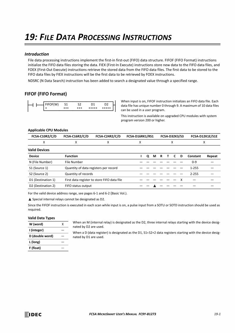
19: FILE DATA PROCESSING INSTRUCTIONS
IntroductionFile data processing instructions implement the first‐in first‐out (FIFO) data structure. FIFOF (FIFO Format) instructions initialize the FIFO data files storing the data. FIEX (First‐In Execute) instructions store new data to the FIFO data files, and FOEX (First‐Out Execute) instructions retrieve the stored data from the FIFO data files. The first data to be stored to the FIFO data files by FIEX instructions will be the first data to be retrieved by FOEX instructions.
NDSRC (N Data Search) instruction has been added to search a designated value through a specified range.
FIFOF (FIFO Format)
Applicable CPU Modules
Valid Devices
For the valid device address range, see pages 6‐1 and 6‐2 (Basic Vol.).
Special internal relays cannot be designated as D2.
Since the FIFOF instruction is executed in each scan while input is on, a pulse input from a SOTU or SOTD instruction should be used as required.
Valid Data Types
FC5A‐C10R2/C/D FC5A‐C16R2/C/D FC5A‐C24R2/C/D FC5A‐D16RK1/RS1 FC5A‐D32K3/S3 FC5A‐D12K1E/S1E
X X X X X X
Device Function I Q M R T C D Constant Repeat
N (File Number) File Number — — — — — — — 0‐9 —
S1 (Source 1) Quantity of data registers per record — — — — — — — 1‐255 —
S2 (Source 2) Quantity of records — — — — — — — 2‐255 —
D1 (Destination 1) First data register to store FIFO data file — — — — — — X — —
D2 (Destination 2) FIFO status output — — — — — — — —
W (word) X
I (integer) —
D (double word) —
L (long) —
F (float) —
When input is on, FIFOF instruction initializes an FIFO data file. Each data file has unique number 0 through 9. A maximum of 10 data files can be used in a user program.
This instruction is available on upgraded CPU modules with system program version 200 or higher.
FIFOF(W)*
S1***
S2***
D1*****
D2*****
When an M (internal relay) is designated as the D2, three internal relays starting with the device desig‐nated by D2 are used.
When a D (data register) is designated as the D1, S1S2+2 data registers starting with the device desig‐nated by D1 are used.
FC5A MICROSMART USER’S MANUAL FC9Y‐B1273 19‐1
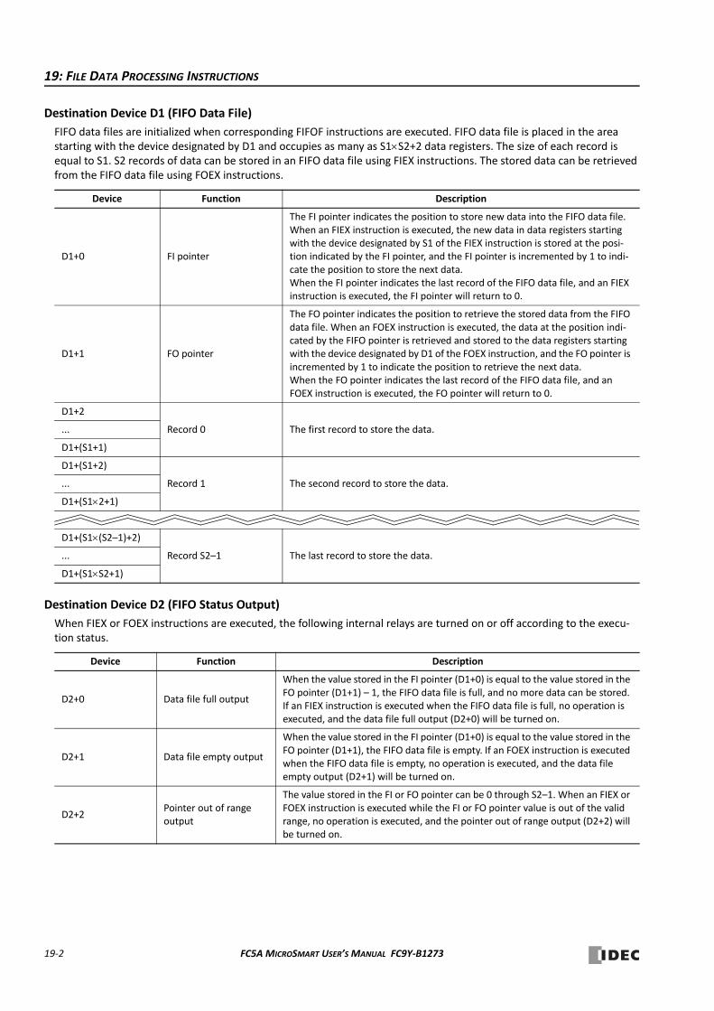
19: FILE DATA PROCESSING INSTRUCTIONS
Destination Device D1 (FIFO Data File)
FIFO data files are initialized when corresponding FIFOF instructions are executed. FIFO data file is placed in the area starting with the device designated by D1 and occupies as many as S1S2+2 data registers. The size of each record is equal to S1. S2 records of data can be stored in an FIFO data file using FIEX instructions. The stored data can be retrieved from the FIFO data file using FOEX instructions.
Destination Device D2 (FIFO Status Output)
When FIEX or FOEX instructions are executed, the following internal relays are turned on or off according to the execu‐tion status.
Device Function Description
D1+0 FI pointer
The FI pointer indicates the position to store new data into the FIFO data file. When an FIEX instruction is executed, the new data in data registers starting with the device designated by S1 of the FIEX instruction is stored at the posi‐tion indicated by the FI pointer, and the FI pointer is incremented by 1 to indi‐cate the position to store the next data.When the FI pointer indicates the last record of the FIFO data file, and an FIEX instruction is executed, the FI pointer will return to 0.
D1+1 FO pointer
The FO pointer indicates the position to retrieve the stored data from the FIFO data file. When an FOEX instruction is executed, the data at the position indi‐cated by the FIFO pointer is retrieved and stored to the data registers starting with the device designated by D1 of the FOEX instruction, and the FO pointer is incremented by 1 to indicate the position to retrieve the next data.When the FO pointer indicates the last record of the FIFO data file, and an FOEX instruction is executed, the FO pointer will return to 0.
D1+2
Record 0 The first record to store the data....
D1+(S1+1)
D1+(S1+2)
Record 1 The second record to store the data....
D1+(S12+1)
D1+(S1(S2–1)+2)
Record S2–1 The last record to store the data....
D1+(S1S2+1)
Device Function Description
D2+0 Data file full output
When the value stored in the FI pointer (D1+0) is equal to the value stored in the FO pointer (D1+1) – 1, the FIFO data file is full, and no more data can be stored. If an FIEX instruction is executed when the FIFO data file is full, no operation is executed, and the data file full output (D2+0) will be turned on.
D2+1 Data file empty output
When the value stored in the FI pointer (D1+0) is equal to the value stored in the FO pointer (D1+1), the FIFO data file is empty. If an FOEX instruction is executed when the FIFO data file is empty, no operation is executed, and the data file empty output (D2+1) will be turned on.
D2+2Pointer out of range output
The value stored in the FI or FO pointer can be 0 through S2–1. When an FIEX or FOEX instruction is executed while the FI or FO pointer value is out of the valid range, no operation is executed, and the pointer out of range output (D2+2) will be turned on.
19‐2 FC5A MICROSMART USER’S MANUAL FC9Y‐B1273
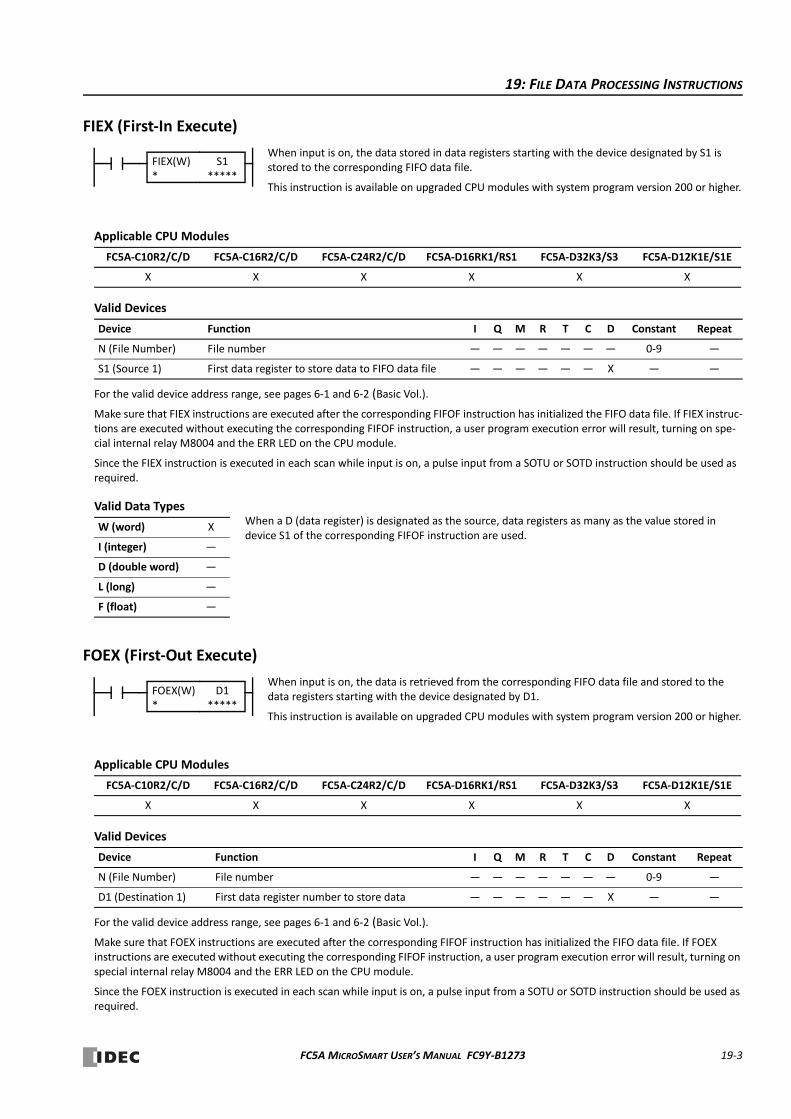
19: FILE DATA PROCESSING INSTRUCTIONS
FIEX (First‐In Execute)
Applicable CPU Modules
Valid Devices
For the valid device address range, see pages 6‐1 and 6‐2 (Basic Vol.).
Make sure that FIEX instructions are executed after the corresponding FIFOF instruction has initialized the FIFO data file. If FIEX instruc‐tions are executed without executing the corresponding FIFOF instruction, a user program execution error will result, turning on spe‐cial internal relay M8004 and the ERR LED on the CPU module.
Since the FIEX instruction is executed in each scan while input is on, a pulse input from a SOTU or SOTD instruction should be used as required.
Valid Data Types
FOEX (First‐Out Execute)
Applicable CPU Modules
Valid Devices
For the valid device address range, see pages 6‐1 and 6‐2 (Basic Vol.).
Make sure that FOEX instructions are executed after the corresponding FIFOF instruction has initialized the FIFO data file. If FOEX instructions are executed without executing the corresponding FIFOF instruction, a user program execution error will result, turning on special internal relay M8004 and the ERR LED on the CPU module.
Since the FOEX instruction is executed in each scan while input is on, a pulse input from a SOTU or SOTD instruction should be used as required.
FC5A‐C10R2/C/D FC5A‐C16R2/C/D FC5A‐C24R2/C/D FC5A‐D16RK1/RS1 FC5A‐D32K3/S3 FC5A‐D12K1E/S1E
X X X X X X
Device Function I Q M R T C D Constant Repeat
N (File Number) File number — — — — — — — 0‐9 —
S1 (Source 1) First data register to store data to FIFO data file — — — — — — X — —
W (word) X
I (integer) —
D (double word) —
L (long) —
F (float) —
FC5A‐C10R2/C/D FC5A‐C16R2/C/D FC5A‐C24R2/C/D FC5A‐D16RK1/RS1 FC5A‐D32K3/S3 FC5A‐D12K1E/S1E
X X X X X X
Device Function I Q M R T C D Constant Repeat
N (File Number) File number — — — — — — — 0‐9 —
D1 (Destination 1) First data register number to store data — — — — — — X — —
When input is on, the data stored in data registers starting with the device designated by S1 is stored to the corresponding FIFO data file.
This instruction is available on upgraded CPU modules with system program version 200 or higher.
FIEX(W)*
S1*****
When a D (data register) is designated as the source, data registers as many as the value stored in device S1 of the corresponding FIFOF instruction are used.
When input is on, the data is retrieved from the corresponding FIFO data file and stored to the data registers starting with the device designated by D1.
This instruction is available on upgraded CPU modules with system program version 200 or higher.
FOEX(W)*
D1*****
FC5A MICROSMART USER’S MANUAL FC9Y‐B1273 19‐3
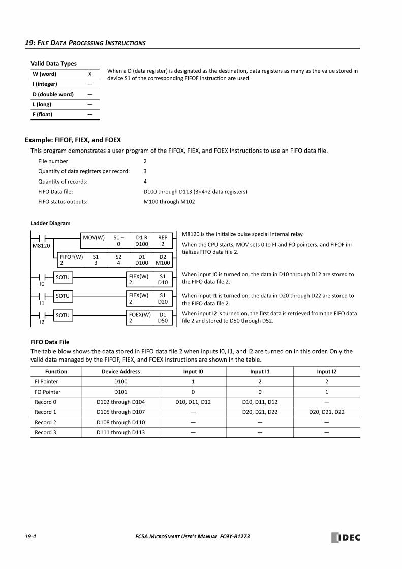
19: FILE DATA PROCESSING INSTRUCTIONS
Valid Data Types
Example: FIFOF, FIEX, and FOEX
This program demonstrates a user program of the FIFOX, FIEX, and FOEX instructions to use an FIFO data file.
File number: 2
Quantity of data registers per record: 3
Quantity of records: 4
FIFO Data file: D100 through D113 (34+2 data registers)
FIFO status outputs: M100 through M102
FIFO Data File
The table blow shows the data stored in FIFO data file 2 when inputs I0, I1, and I2 are turned on in this order. Only the valid data managed by the FIFOF, FIEX, and FOEX instructions are shown in the table.
W (word) X
I (integer) —
D (double word) —
L (long) —
F (float) —
Function Device Address Input I0 Input I1 Input I2
FI Pointer D100 1 2 2
FO Pointer D101 0 0 1
Record 0 D102 through D104 D10, D11, D12 D10, D11, D12 —
Record 1 D105 through D107 — D20, D21, D22 D20, D21, D22
Record 2 D108 through D110 — — —
Record 3 D111 through D113 — — —
When a D (data register) is designated as the destination, data registers as many as the value stored in device S1 of the corresponding FIFOF instruction are used.
I0S1D10
FIEX(W)2
M8120
SOTU
Ladder Diagram
M8120 is the initialize pulse special internal relay.
When the CPU starts, MOV sets 0 to FI and FO pointers, and FIFOF ini‐tializes FIFO data file 2.
When input I0 is turned on, the data in D10 through D12 are stored to the FIFO data file 2.
When input I1 is turned on, the data in D20 through D22 are stored to the FIFO data file 2.
When input I2 is turned on, the first data is retrieved from the FIFO data file 2 and stored to D50 through D52.
REP2
S1 –0
D1 RD100
MOV(W)
D2M100
S13
D1D100
FIFOF(W)2
S24
I1S1D20
FIEX(W)2
I2D1D50
FOEX(W)2
SOTU
SOTU
19‐4 FC5A MICROSMART USER’S MANUAL FC9Y‐B1273
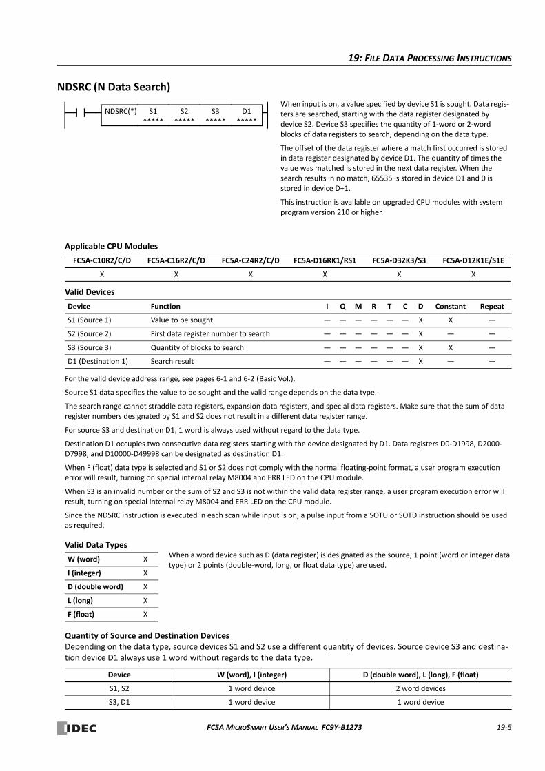
19: FILE DATA PROCESSING INSTRUCTIONS
NDSRC (N Data Search)
Applicable CPU Modules
Valid Devices
For the valid device address range, see pages 6‐1 and 6‐2 (Basic Vol.).
Source S1 data specifies the value to be sought and the valid range depends on the data type.
The search range cannot straddle data registers, expansion data registers, and special data registers. Make sure that the sum of data register numbers designated by S1 and S2 does not result in a different data register range.
For source S3 and destination D1, 1 word is always used without regard to the data type.
Destination D1 occupies two consecutive data registers starting with the device designated by D1. Data registers D0‐D1998, D2000‐D7998, and D10000‐D49998 can be designated as destination D1.
When F (float) data type is selected and S1 or S2 does not comply with the normal floating‐point format, a user program execution error will result, turning on special internal relay M8004 and ERR LED on the CPU module.
When S3 is an invalid number or the sum of S2 and S3 is not within the valid data register range, a user program execution error will result, turning on special internal relay M8004 and ERR LED on the CPU module.
Since the NDSRC instruction is executed in each scan while input is on, a pulse input from a SOTU or SOTD instruction should be used as required.
Valid Data Types
Quantity of Source and Destination DevicesDepending on the data type, source devices S1 and S2 use a different quantity of devices. Source device S3 and destina‐tion device D1 always use 1 word without regards to the data type.
FC5A‐C10R2/C/D FC5A‐C16R2/C/D FC5A‐C24R2/C/D FC5A‐D16RK1/RS1 FC5A‐D32K3/S3 FC5A‐D12K1E/S1E
X X X X X X
Device Function I Q M R T C D Constant Repeat
S1 (Source 1) Value to be sought — — — — — — X X —
S2 (Source 2) First data register number to search — — — — — — X — —
S3 (Source 3) Quantity of blocks to search — — — — — — X X —
D1 (Destination 1) Search result — — — — — — X — —
W (word) X
I (integer) X
D (double word) X
L (long) X
F (float) X
Device W (word), I (integer) D (double word), L (long), F (float)
S1, S2 1 word device 2 word devices
S3, D1 1 word device 1 word device
When input is on, a value specified by device S1 is sought. Data regis‐ters are searched, starting with the data register designated by device S2. Device S3 specifies the quantity of 1‐word or 2‐word blocks of data registers to search, depending on the data type.
The offset of the data register where a match first occurred is stored in data register designated by device D1. The quantity of times the value was matched is stored in the next data register. When the search results in no match, 65535 is stored in device D1 and 0 is stored in device D+1.
This instruction is available on upgraded CPU modules with system program version 210 or higher.
NDSRC(*) S1*****
S2*****
S3*****
D1*****
When a word device such as D (data register) is designated as the source, 1 point (word or integer data type) or 2 points (double‐word, long, or float data type) are used.
FC5A MICROSMART USER’S MANUAL FC9Y‐B1273 19‐5
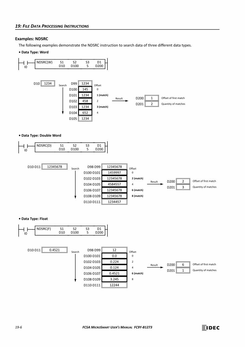
19: FILE DATA PROCESSING INSTRUCTIONS
Examples: NDSRC
The following examples demonstrate the NDSRC instruction to search data of three different data types.
• Data Type: Word
• Data Type: Double Word
• Data Type: Float
I0
D1D200
S1D10
S35
NDSRC(W) S2D100
1234D10 1234D99
145D100
1234D101
458D102
1234D103
652D104
1234D105
Offset
0
1 (match)
2
3 (match)
4
Search
1D200Result
2D201
Offset of first match
Quantity of matches
I0
D1D200
S1D10
S35
NDSRC(D) S2D100
Offset
0
2 (match)
4
6 (match)
8 (match)
Search
2D200Result
3D201
12345678D98∙D99
Offset of first match
Quantity of matches
12345678D10∙D11
1459997D100∙D101
12345678D102∙D103
4584557D104∙D105
12345678D106∙D107
12345678D108∙D109
1234457D110∙D111
I0
D1D200
S1D10
S35
NDSRC(F) S2D100
Offset
0
2
4
6 (match)
8
Search
6D200Result
1D201
12D98∙D99
Offset of first match
Quantity of matches
0.4521D10∙D11
0.0D100∙D101
0.224D102∙D103
0.124D104∙D105
0.4521D106∙D107
3.245D108∙D109
12244D110∙D111
19‐6 FC5A MICROSMART USER’S MANUAL FC9Y‐B1273
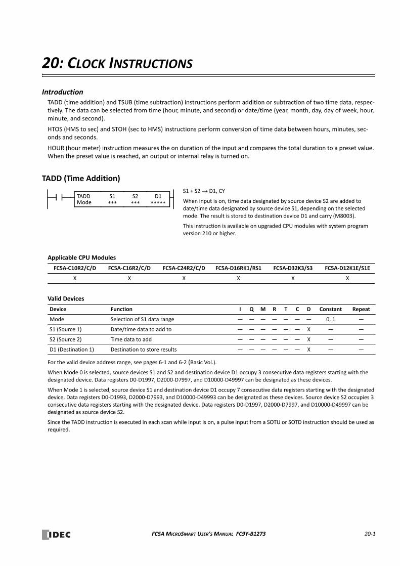
20: CLOCK INSTRUCTIONS
IntroductionTADD (time addition) and TSUB (time subtraction) instructions perform addition or subtraction of two time data, respec‐tively. The data can be selected from time (hour, minute, and second) or date/time (year, month, day, day of week, hour, minute, and second).
HTOS (HMS to sec) and STOH (sec to HMS) instructions perform conversion of time data between hours, minutes, sec‐onds and seconds.
HOUR (hour meter) instruction measures the on duration of the input and compares the total duration to a preset value. When the preset value is reached, an output or internal relay is turned on.
TADD (Time Addition)
Applicable CPU Modules
Valid Devices
For the valid device address range, see pages 6‐1 and 6‐2 (Basic Vol.).
When Mode 0 is selected, source devices S1 and S2 and destination device D1 occupy 3 consecutive data registers starting with the designated device. Data registers D0‐D1997, D2000‐D7997, and D10000‐D49997 can be designated as these devices.
When Mode 1 is selected, source device S1 and destination device D1 occupy 7 consecutive data registers starting with the designated device. Data registers D0‐D1993, D2000‐D7993, and D10000‐D49993 can be designated as these devices. Source device S2 occupies 3 consecutive data registers starting with the designated device. Data registers D0‐D1997, D2000‐D7997, and D10000‐D49997 can be designated as source device S2.
Since the TADD instruction is executed in each scan while input is on, a pulse input from a SOTU or SOTD instruction should be used as required.
FC5A‐C10R2/C/D FC5A‐C16R2/C/D FC5A‐C24R2/C/D FC5A‐D16RK1/RS1 FC5A‐D32K3/S3 FC5A‐D12K1E/S1E
X X X X X X
Device Function I Q M R T C D Constant Repeat
Mode Selection of S1 data range — — — — — — — 0, 1 —
S1 (Source 1) Date/time data to add to — — — — — — X — —
S2 (Source 2) Time data to add — — — — — — X — —
D1 (Destination 1) Destination to store results — — — — — — X — —
S1 + S2 D1, CY
When input is on, time data designated by source device S2 are added to date/time data designated by source device S1, depending on the selected mode. The result is stored to destination device D1 and carry (M8003).
This instruction is available on upgraded CPU modules with system program version 210 or higher.
S1***
S2***
D1*****
TADDMode
FC5A MICROSMART USER’S MANUAL FC9Y‐B1273 20‐1
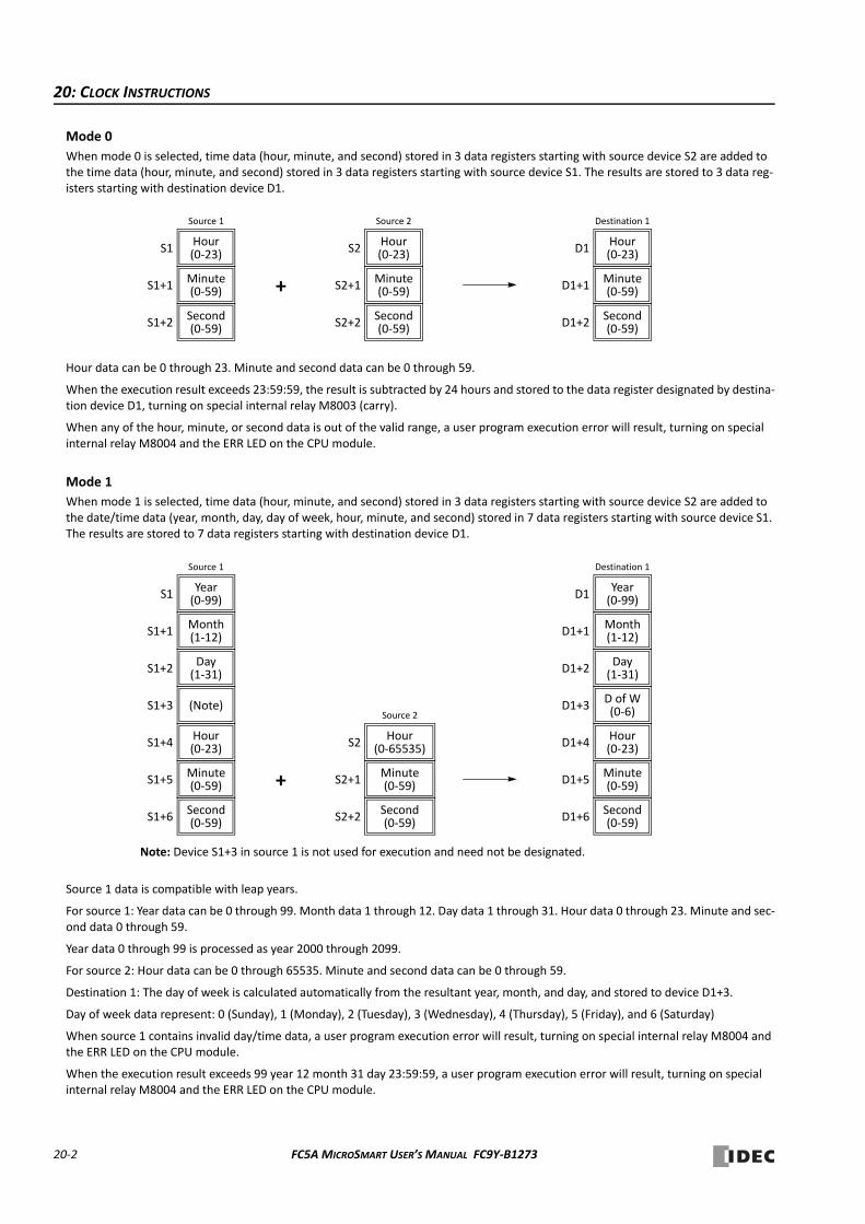
20: CLOCK INSTRUCTIONS
Mode 0
When mode 0 is selected, time data (hour, minute, and second) stored in 3 data registers starting with source device S2 are added to the time data (hour, minute, and second) stored in 3 data registers starting with source device S1. The results are stored to 3 data reg‐isters starting with destination device D1.
Hour data can be 0 through 23. Minute and second data can be 0 through 59.
When the execution result exceeds 23:59:59, the result is subtracted by 24 hours and stored to the data register designated by destina‐tion device D1, turning on special internal relay M8003 (carry).
When any of the hour, minute, or second data is out of the valid range, a user program execution error will result, turning on special internal relay M8004 and the ERR LED on the CPU module.
Mode 1
When mode 1 is selected, time data (hour, minute, and second) stored in 3 data registers starting with source device S2 are added to the date/time data (year, month, day, day of week, hour, minute, and second) stored in 7 data registers starting with source device S1. The results are stored to 7 data registers starting with destination device D1.
Source 1 data is compatible with leap years.
For source 1: Year data can be 0 through 99. Month data 1 through 12. Day data 1 through 31. Hour data 0 through 23. Minute and sec‐ond data 0 through 59.
Year data 0 through 99 is processed as year 2000 through 2099.
For source 2: Hour data can be 0 through 65535. Minute and second data can be 0 through 59.
Destination 1: The day of week is calculated automatically from the resultant year, month, and day, and stored to device D1+3.
Day of week data represent: 0 (Sunday), 1 (Monday), 2 (Tuesday), 3 (Wednesday), 4 (Thursday), 5 (Friday), and 6 (Saturday)
When source 1 contains invalid day/time data, a user program execution error will result, turning on special internal relay M8004 and the ERR LED on the CPU module.
When the execution result exceeds 99 year 12 month 31 day 23:59:59, a user program execution error will result, turning on special internal relay M8004 and the ERR LED on the CPU module.
Source 1
HourS1 (0‐23)
MinuteS1+1 (0‐59)
SecondS1+2 (0‐59)
Source 2
HourS2 (0‐23)
MinuteS2+1 (0‐59)
SecondS2+2 (0‐59)
+
Destination 1
HourD1 (0‐23)
MinuteD1+1 (0‐59)
SecondD1+2 (0‐59)
Source 1
YearS1 (0‐99)
MonthS1+1 (1‐12)
DayS1+2 (1‐31)
Source 2
HourS2 (0‐65535)
MinuteS2+1 (0‐59)
SecondS2+2 (0‐59)
+
Destination 1
YearD1 (0‐99)
MonthD1+1 (1‐12)
DayD1+2 (1‐31)
HourS1+4 (0‐23)
MinuteS1+5 (0‐59)
SecondS1+6 (0‐59)
S1+3 (Note)
HourD1+4 (0‐23)
MinuteD1+5 (0‐59)
SecondD1+6 (0‐59)
D of WD1+3 (0‐6)
Note: Device S1+3 in source 1 is not used for execution and need not be designated.
20‐2 FC5A MICROSMART USER’S MANUAL FC9Y‐B1273
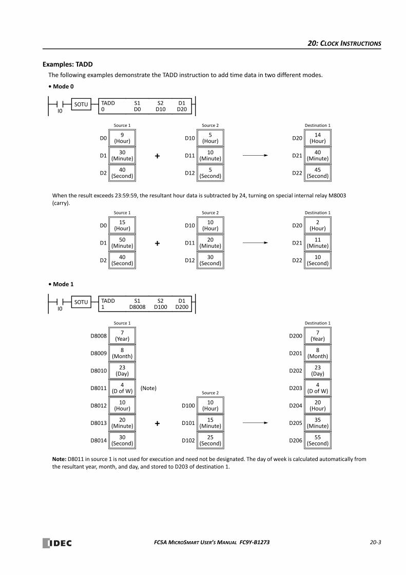
20: CLOCK INSTRUCTIONS
Examples: TADD
The following examples demonstrate the TADD instruction to add time data in two different modes.
• Mode 0
• Mode 1
I0
D1D20
S1D0
S2D10
TADD0
Source 1
9D0 (Hour)
30D1 (Minute)
40D2 (Second)
Source 2
5D10 (Hour)
10D11 (Minute)
5D12 (Second)
+
Destination 1
14D20 (Hour)
40D21 (Minute)
45D22 (Second)
When the result exceeds 23:59:59, the resultant hour data is subtracted by 24, turning on special internal relay M8003 (carry).
Source 1
15D0 (Hour)
50D1 (Minute)
40D2 (Second)
Source 2
10D10 (Hour)
20D11 (Minute)
30D12 (Second)
+
Destination 1
2D20 (Hour)
11D21 (Minute)
10D22 (Second)
SOTU
I0
D1D200
S1D8008
S2D100
TADD1
Source 2
10D100 (Hour)
15D101 (Minute)
25D102 (Second)
Source 1
7D8008 (Year)
8D8009 (Month)
23D8010 (Day)
+
Destination 1
10D8012 (Hour)
20D8013 (Minute)
30D8014 (Second)
D8011 (Note)
7D200 (Year)
8D201 (Month)
23D202 (Day)
20D204 (Hour)
35D205 (Minute)
55D206 (Second)
4D203 (D of W)
Note: D8011 in source 1 is not used for execution and need not be designated. The day of week is calculated automatically from the resultant year, month, and day, and stored to D203 of destination 1.
4(D of W)
SOTU
FC5A MICROSMART USER’S MANUAL FC9Y‐B1273 20‐3

20: CLOCK INSTRUCTIONS
Source 2
30D100 (Hour)
35D101 (Minute)
15D102 (Second)
When the result exceeds 23:59:59, the resultant hour data is subtracted by a multiple of 24 and the day data is incremented.
Source 1
7D8008 (Year)
8D8009 (Month)
23D8010 (Day)
+
Destination 1
20D8012 (Hour)
30D8013 (Minute)
40D8014 (Second)
4D8011 (D of W)
7D200 (Year)
8D201 (Month)
25D202 (Day)
3D204 (Hour)
5D205 (Minute)
55D206 (Second)
6D203 (D of W)(Note)
Note: D8011 in source 1 is not used for execution and need not be designated. The day of week is calculated automatically from the resultant year, month, and day, and stored to D203 of destination 1.
20‐4 FC5A MICROSMART USER’S MANUAL FC9Y‐B1273
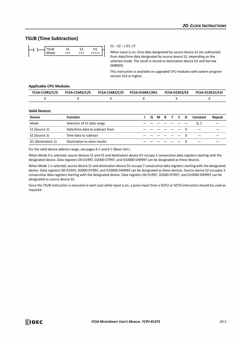
20: CLOCK INSTRUCTIONS
TSUB (Time Subtraction)
Applicable CPU Modules
Valid Devices
For the valid device address range, see pages 6‐1 and 6‐2 (Basic Vol.).
When Mode 0 is selected, source devices S1 and S2 and destination device D1 occupy 3 consecutive data registers starting with the designated device. Data registers D0‐D1997, D2000‐D7997, and D10000‐D49997 can be designated as these devices.
When Mode 1 is selected, source device S1 and destination device D1 occupy 7 consecutive data registers starting with the designated device. Data registers D0‐D1993, D2000‐D7993, and D10000‐D49993 can be designated as these devices. Source device S2 occupies 3 consecutive data registers starting with the designated device. Data registers D0‐D1997, D2000‐D7997, and D10000‐D49997 can be designated as source device S2.
Since the TSUB instruction is executed in each scan while input is on, a pulse input from a SOTU or SOTD instruction should be used as required.
FC5A‐C10R2/C/D FC5A‐C16R2/C/D FC5A‐C24R2/C/D FC5A‐D16RK1/RS1 FC5A‐D32K3/S3 FC5A‐D12K1E/S1E
X X X X X X
Device Function I Q M R T C D Constant Repeat
Mode Selection of S1 data range — — — — — — — 0, 1 —
S1 (Source 1) Date/time data to subtract from — — — — — — X — —
S2 (Source 2) Time data to subtract — — — — — — X — —
D1 (Destination 1) Destination to store results — — — — — — X — —
S1 – S2 D1, CY
When input is on, time data designated by source device S2 are subtracted from date/time data designated by source device S1, depending on the selected mode. The result is stored to destination device D1 and borrow (M8003).
This instruction is available on upgraded CPU modules with system program version 210 or higher.
S1***
S2***
D1*****
TSUBMode
FC5A MICROSMART USER’S MANUAL FC9Y‐B1273 20‐5
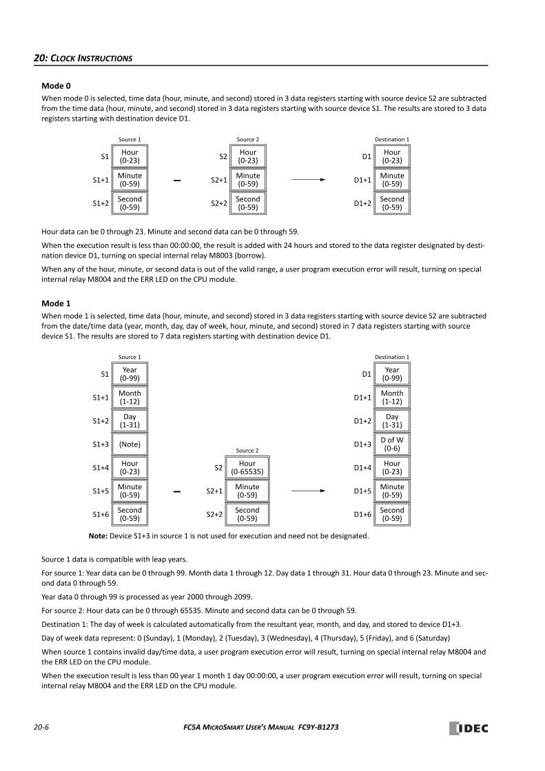
20: CLOCK INSTRUCTIONS
Mode 0
When mode 0 is selected, time data (hour, minute, and second) stored in 3 data registers starting with source device S2 are subtracted from the time data (hour, minute, and second) stored in 3 data registers starting with source device S1. The results are stored to 3 data registers starting with destination device D1.
Hour data can be 0 through 23. Minute and second data can be 0 through 59.
When the execution result is less than 00:00:00, the result is added with 24 hours and stored to the data register designated by desti‐nation device D1, turning on special internal relay M8003 (borrow).
When any of the hour, minute, or second data is out of the valid range, a user program execution error will result, turning on special internal relay M8004 and the ERR LED on the CPU module.
Mode 1
When mode 1 is selected, time data (hour, minute, and second) stored in 3 data registers starting with source device S2 are subtracted from the date/time data (year, month, day, day of week, hour, minute, and second) stored in 7 data registers starting with source device S1. The results are stored to 7 data registers starting with destination device D1.
Source 1 data is compatible with leap years.
For source 1: Year data can be 0 through 99. Month data 1 through 12. Day data 1 through 31. Hour data 0 through 23. Minute and sec‐ond data 0 through 59.
Year data 0 through 99 is processed as year 2000 through 2099.
For source 2: Hour data can be 0 through 65535. Minute and second data can be 0 through 59.
Destination 1: The day of week is calculated automatically from the resultant year, month, and day, and stored to device D1+3.
Day of week data represent: 0 (Sunday), 1 (Monday), 2 (Tuesday), 3 (Wednesday), 4 (Thursday), 5 (Friday), and 6 (Saturday)
When source 1 contains invalid day/time data, a user program execution error will result, turning on special internal relay M8004 and the ERR LED on the CPU module.
When the execution result is less than 00 year 1 month 1 day 00:00:00, a user program execution error will result, turning on special internal relay M8004 and the ERR LED on the CPU module.
Source 1
HourS1 (0‐23)
MinuteS1+1 (0‐59)
SecondS1+2 (0‐59)
Source 2
HourS2 (0‐23)
MinuteS2+1 (0‐59)
SecondS2+2 (0‐59)
–
Destination 1
HourD1 (0‐23)
MinuteD1+1 (0‐59)
SecondD1+2 (0‐59)
Source 1
YearS1 (0‐99)
MonthS1+1 (1‐12)
DayS1+2 (1‐31)
–
Destination 1
YearD1 (0‐99)
MonthD1+1 (1‐12)
DayD1+2 (1‐31)
HourS1+4 (0‐23)
MinuteS1+5 (0‐59)
SecondS1+6 (0‐59)
S1+3
HourD1+4 (0‐23)
MinuteD1+5 (0‐59)
SecondD1+6 (0‐59)
D of WD1+3 (0‐6)Source 2
HourS2 (0‐65535)
MinuteS2+1 (0‐59)
SecondS2+2 (0‐59)
(Note)
Note: Device S1+3 in source 1 is not used for execution and need not be designated.
20‐6 FC5A MICROSMART USER’S MANUAL FC9Y‐B1273
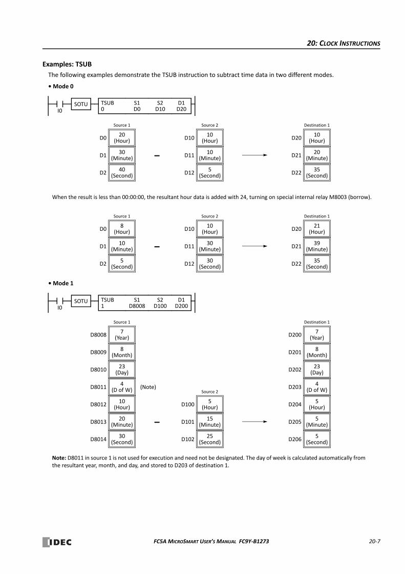
20: CLOCK INSTRUCTIONS
Examples: TSUB
The following examples demonstrate the TSUB instruction to subtract time data in two different modes.
• Mode 0
• Mode 1
I0
D1D20
S1D0
S2D10
TSUB0
Source 1
20D0 (Hour)
30D1 (Minute)
40D2 (Second)
Source 2
10D10 (Hour)
10D11 (Minute)
5D12 (Second)
–
Destination 1
10D20 (Hour)
20D21 (Minute)
35D22 (Second)
When the result is less than 00:00:00, the resultant hour data is added with 24, turning on special internal relay M8003 (borrow).
Source 1
8D0 (Hour)
10D1 (Minute)
5D2 (Second)
Source 2
10D10 (Hour)
30D11 (Minute)
30D12 (Second)
–
Destination 1
21D20 (Hour)
39D21 (Minute)
35D22 (Second)
SOTU
I0
D1D200
S1D8008
S2D100
TSUB1
Source 2
5D100 (Hour)
15D101 (Minute)
25D102 (Second)
Source 1
7D8008 (Year)
8D8009 (Month)
23D8010 (Day)
–
Destination 1
10D8012 (Hour)
20D8013 (Minute)
30D8014 (Second)
4D8011 (D of W)
7D200 (Year)
8D201 (Month)
23D202 (Day)
5D204 (Hour)
5D205 (Minute)
5D206 (Second)
4D203 (D of W)
SOTU
(Note)
Note: D8011 in source 1 is not used for execution and need not be designated. The day of week is calculated automatically from the resultant year, month, and day, and stored to D203 of destination 1.
FC5A MICROSMART USER’S MANUAL FC9Y‐B1273 20‐7
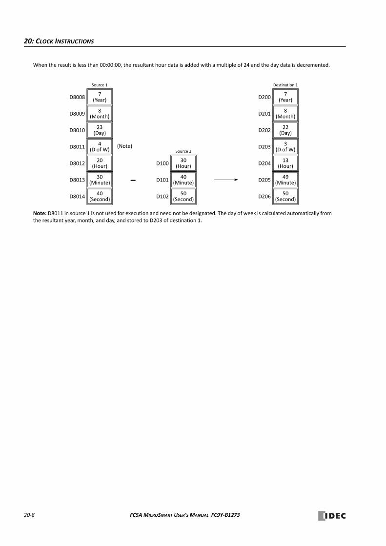
20: CLOCK INSTRUCTIONS
Source 2
30D100 (Hour)
40D101 (Minute)
50D102 (Second)
When the result is less than 00:00:00, the resultant hour data is added with a multiple of 24 and the day data is decremented.
Source 1
7D8008 (Year)
8D8009 (Month)
23D8010 (Day)
–
Destination 1
20D8012 (Hour)
30D8013 (Minute)
40D8014 (Second)
4D8011 (D of W)
7D200 (Year)
8D201 (Month)
22D202 (Day)
13D204 (Hour)
49D205 (Minute)
50D206 (Second)
3D203 (D of W)
(Note)
Note: D8011 in source 1 is not used for execution and need not be designated. The day of week is calculated automatically from the resultant year, month, and day, and stored to D203 of destination 1.
20‐8 FC5A MICROSMART USER’S MANUAL FC9Y‐B1273
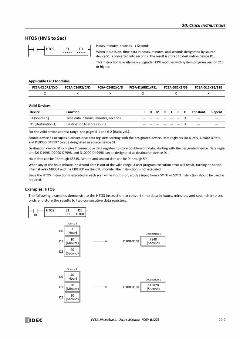
20: CLOCK INSTRUCTIONS
HTOS (HMS to Sec)
Applicable CPU Modules
Valid Devices
For the valid device address range, see pages 6‐1 and 6‐2 (Basic Vol.).
Source device S1 occupies 3 consecutive data registers starting with the designated device. Data registers D0‐D1997, D2000‐D7997, and D10000‐D49997 can be designated as source device S1.
Destination device D1 occupies 2 consecutive data registers to store double‐word data, starting with the designated device. Data regis‐ters D0‐D1998, D2000‐D7998, and D10000‐D49998 can be designated as destination device D1.
Hour data can be 0 through 65535. Minute and second data can be 0 through 59.
When any of the hour, minute, or second data is out of the valid range, a user program execution error will result, turning on special internal relay M8004 and the ERR LED on the CPU module. The instruction is not executed.
Since the HTOS instruction is executed in each scan while input is on, a pulse input from a SOTU or SOTD instruction should be used as required.
Examples: HTOS
The following examples demonstrate the HTOS instruction to convert time data in hours, minutes, and seconds into sec‐onds and store the results to two consecutive data registers.
FC5A‐C10R2/C/D FC5A‐C16R2/C/D FC5A‐C24R2/C/D FC5A‐D16RK1/RS1 FC5A‐D32K3/S3 FC5A‐D12K1E/S1E
X X X X X X
Device Function I Q M R T C D Constant Repeat
S1 (Source 1) Time data in hours, minutes, seconds — — — — — — X — —
D1 (Destination 1) Destination to store results — — — — — — X — —
Hours, minutes, seconds Seconds
When input is on, time data in hours, minutes, and seconds designated by source device S1 is converted into seconds. The result is stored to destination device D1.
This instruction is available on upgraded CPU modules with system program version 210 or higher.
S1*****
D1*****
HTOS
I0
D1D100
S1D0
HTOS
Source 1
2D0 (Hour)
10D1 (Minute)
40D2 (Second)
7840D100∙D101 (Second)
Destination 1
Source 1
40D0 (Hour)
30D1 (Minute)
20D2 (Second)
145820D100∙D101 (Second)
Destination 1
FC5A MICROSMART USER’S MANUAL FC9Y‐B1273 20‐9
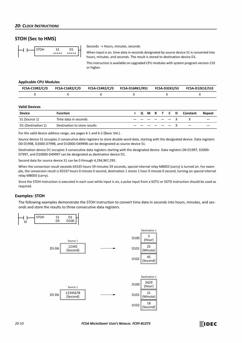
20: CLOCK INSTRUCTIONS
STOH (Sec to HMS)
Applicable CPU Modules
Valid Devices
For the valid device address range, see pages 6‐1 and 6‐2 (Basic Vol.).
Source device S1 occupies 2 consecutive data registers to store double‐word data, starting with the designated device. Data registers D0‐D1998, D2000‐D7998, and D10000‐D49998 can be designated as source device S1.
Destination device D1 occupies 3 consecutive data registers starting with the designated device. Data registers D0‐D1997, D2000‐D7997, and D10000‐D49997 can be designated as destination device D1.
Second data for source device S1 can be 0 through 4,294,967,295.
When the conversion result exceeds 65535 hours 59 minutes 59 seconds, special internal relay M8003 (carry) is turned on. For exam‐ple, the conversion result is 65537 hours 0 minute 0 second, destination 1 stores 1 hour 0 minute 0 second, turning on special internal relay M8003 (carry).
Since the STOH instruction is executed in each scan while input is on, a pulse input from a SOTU or SOTD instruction should be used as required.
Examples: STOH
The following examples demonstrate the STOH instruction to convert time data in seconds into hours, minutes, and sec‐onds and store the results to three consecutive data registers.
FC5A‐C10R2/C/D FC5A‐C16R2/C/D FC5A‐C24R2/C/D FC5A‐D16RK1/RS1 FC5A‐D32K3/S3 FC5A‐D12K1E/S1E
X X X X X X
Device Function I Q M R T C D Constant Repeat
S1 (Source 1) Time data in seconds — — — — — — X X —
D1 (Destination 1) Destination to store results — — — — — — X — —
Seconds Hours, minutes, seconds
When input is on, time data in seconds designated by source device S1 is converted into hours, minutes, and seconds. The result is stored to destination device D1.
This instruction is available on upgraded CPU modules with system program version 210 or higher.
S1*****
D1*****
STOH
I0
D1D100
S1D5
STOH
Destination 1
3D100 (Hour)
25D101 (Minute)
45D102 (Second)
12345D5∙D6 (Second)
Source 1
Destination 1
3429D100 (Hour)
21D101 (Minute)
18D102 (Second)
12345678D5∙D6 (Second)
Source 1
20‐10 FC5A MICROSMART USER’S MANUAL FC9Y‐B1273
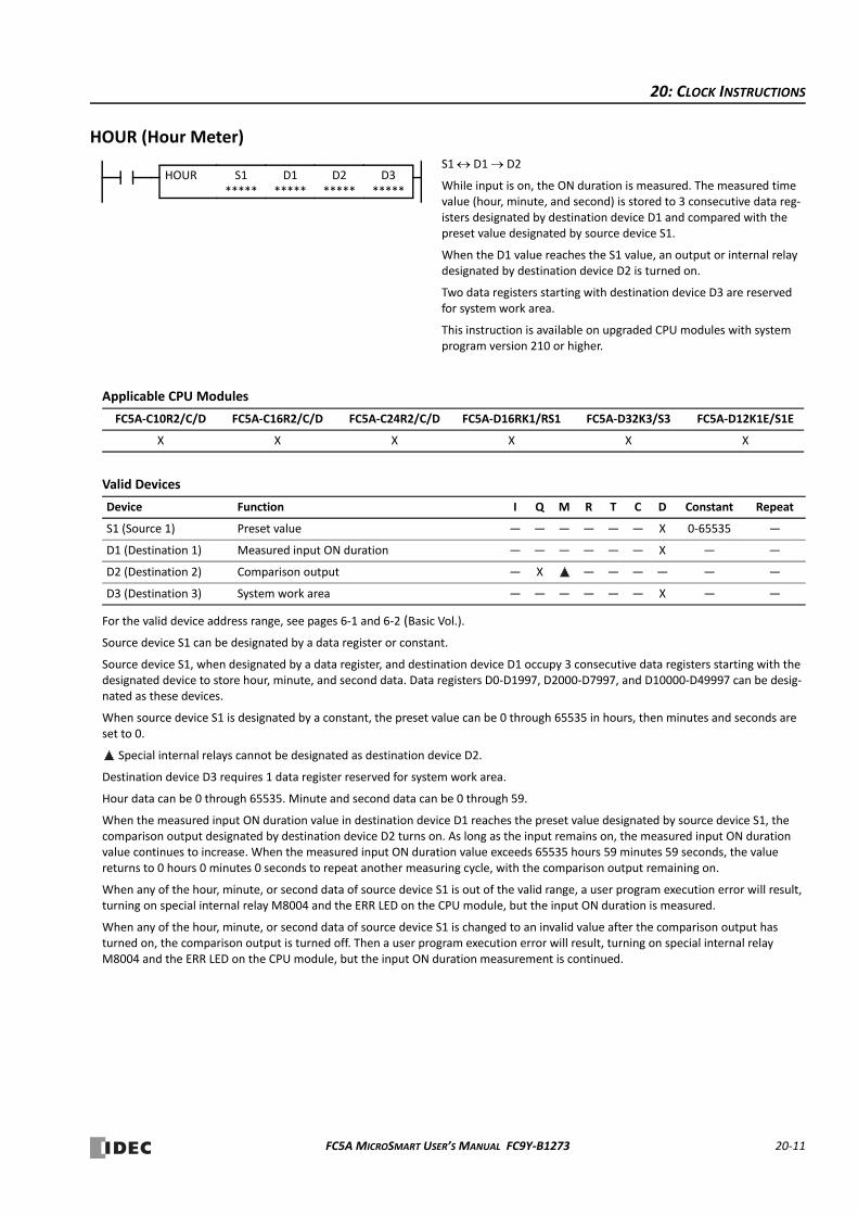
20: CLOCK INSTRUCTIONS
HOUR (Hour Meter)
Applicable CPU Modules
Valid Devices
For the valid device address range, see pages 6‐1 and 6‐2 (Basic Vol.).
Source device S1 can be designated by a data register or constant.
Source device S1, when designated by a data register, and destination device D1 occupy 3 consecutive data registers starting with the designated device to store hour, minute, and second data. Data registers D0‐D1997, D2000‐D7997, and D10000‐D49997 can be desig‐nated as these devices.
When source device S1 is designated by a constant, the preset value can be 0 through 65535 in hours, then minutes and seconds are set to 0.
Special internal relays cannot be designated as destination device D2.
Destination device D3 requires 1 data register reserved for system work area.
Hour data can be 0 through 65535. Minute and second data can be 0 through 59.
When the measured input ON duration value in destination device D1 reaches the preset value designated by source device S1, the comparison output designated by destination device D2 turns on. As long as the input remains on, the measured input ON duration value continues to increase. When the measured input ON duration value exceeds 65535 hours 59 minutes 59 seconds, the value returns to 0 hours 0 minutes 0 seconds to repeat another measuring cycle, with the comparison output remaining on.
When any of the hour, minute, or second data of source device S1 is out of the valid range, a user program execution error will result, turning on special internal relay M8004 and the ERR LED on the CPU module, but the input ON duration is measured.
When any of the hour, minute, or second data of source device S1 is changed to an invalid value after the comparison output has turned on, the comparison output is turned off. Then a user program execution error will result, turning on special internal relay M8004 and the ERR LED on the CPU module, but the input ON duration measurement is continued.
FC5A‐C10R2/C/D FC5A‐C16R2/C/D FC5A‐C24R2/C/D FC5A‐D16RK1/RS1 FC5A‐D32K3/S3 FC5A‐D12K1E/S1E
X X X X X X
Device Function I Q M R T C D Constant Repeat
S1 (Source 1) Preset value — — — — — — X 0‐65535 —
D1 (Destination 1) Measured input ON duration — — — — — — X — —
D2 (Destination 2) Comparison output — X — — — — — —
D3 (Destination 3) System work area — — — — — — X — —
S1 D1 D2
While input is on, the ON duration is measured. The measured time value (hour, minute, and second) is stored to 3 consecutive data reg‐isters designated by destination device D1 and compared with the preset value designated by source device S1.
When the D1 value reaches the S1 value, an output or internal relay designated by destination device D2 is turned on.
Two data registers starting with destination device D3 are reserved for system work area.
This instruction is available on upgraded CPU modules with system program version 210 or higher.
S1*****
D1*****
D3*****
HOUR D2*****
FC5A MICROSMART USER’S MANUAL FC9Y‐B1273 20‐11
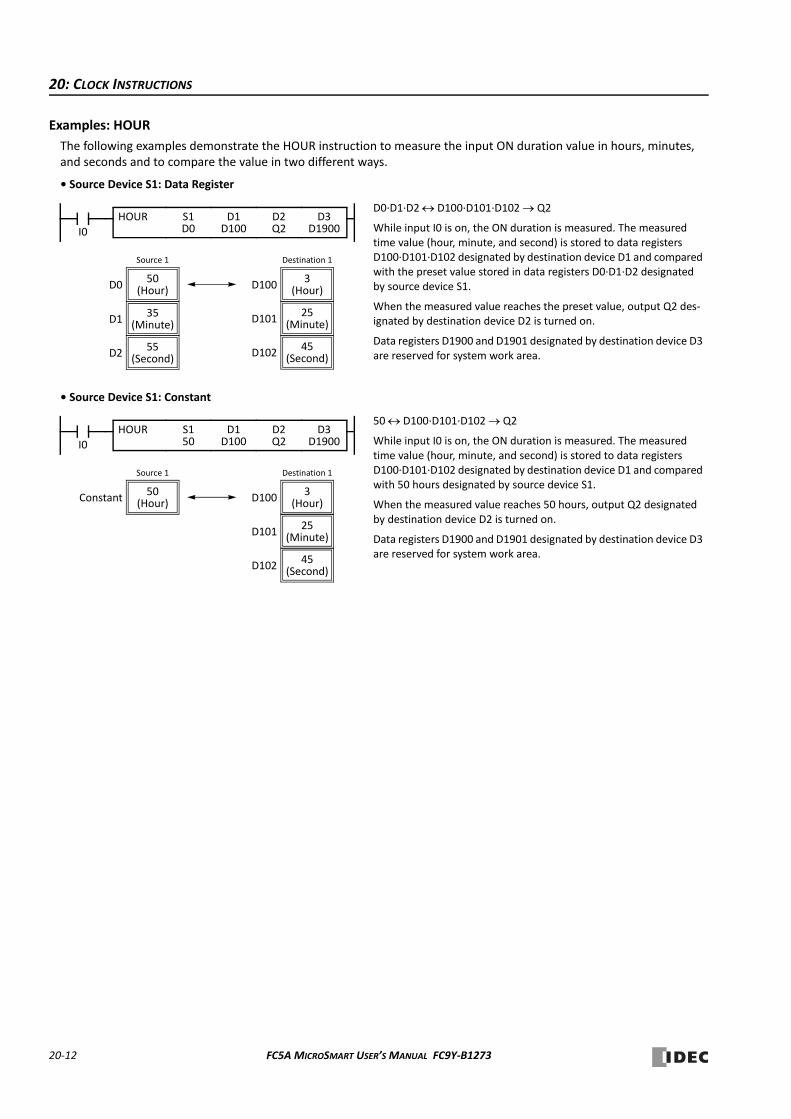
20: CLOCK INSTRUCTIONS
Examples: HOUR
The following examples demonstrate the HOUR instruction to measure the input ON duration value in hours, minutes, and seconds and to compare the value in two different ways.
• Source Device S1: Data Register
• Source Device S1: Constant
I0
D3D1900
S1D0
HOUR
Destination 1
3D100 (Hour)
25D101 (Minute)
45D102 (Second)
D1D100
D2Q2
Source 1
50D0 (Hour)
D0∙D1∙D2 D100∙D101∙D102 Q2
While input I0 is on, the ON duration is measured. The measured time value (hour, minute, and second) is stored to data registers D100∙D101∙D102 designated by destination device D1 and compared with the preset value stored in data registers D0∙D1∙D2 designated by source device S1.
When the measured value reaches the preset value, output Q2 des‐ignated by destination device D2 is turned on.
Data registers D1900 and D1901 designated by destination device D3 are reserved for system work area.
35D1 (Minute)
55D2 (Second)
I0
D3D1900
S150
HOUR
Destination 1
3D100 (Hour)
25D101 (Minute)
45D102 (Second)
D1D100
D2Q2
Source 1
50Constant (Hour)
50 D100∙D101∙D102 Q2
While input I0 is on, the ON duration is measured. The measured time value (hour, minute, and second) is stored to data registers D100∙D101∙D102 designated by destination device D1 and compared with 50 hours designated by source device S1.
When the measured value reaches 50 hours, output Q2 designated by destination device D2 is turned on.
Data registers D1900 and D1901 designated by destination device D3 are reserved for system work area.
20‐12 FC5A MICROSMART USER’S MANUAL FC9Y‐B1273
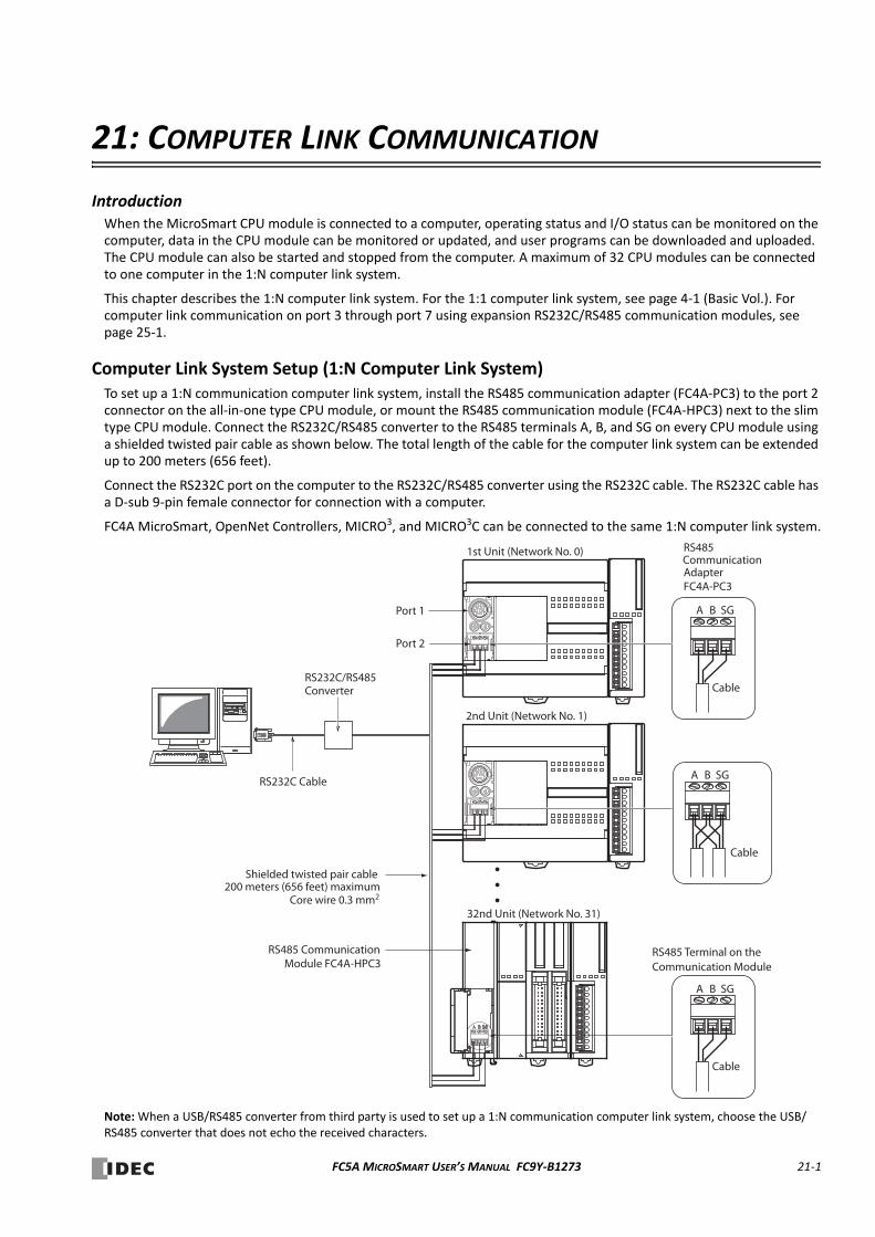
21: COMPUTER LINK COMMUNICATION
IntroductionWhen the MicroSmart CPU module is connected to a computer, operating status and I/O status can be monitored on the computer, data in the CPU module can be monitored or updated, and user programs can be downloaded and uploaded. The CPU module can also be started and stopped from the computer. A maximum of 32 CPU modules can be connected to one computer in the 1:N computer link system.
This chapter describes the 1:N computer link system. For the 1:1 computer link system, see page 4‐1 (Basic Vol.). For computer link communication on port 3 through port 7 using expansion RS232C/RS485 communication modules, see page 25‐1.
Computer Link System Setup (1:N Computer Link System)To set up a 1:N communication computer link system, install the RS485 communication adapter (FC4A‐PC3) to the port 2 connector on the all‐in‐one type CPU module, or mount the RS485 communication module (FC4A‐HPC3) next to the slim type CPU module. Connect the RS232C/RS485 converter to the RS485 terminals A, B, and SG on every CPU module using a shielded twisted pair cable as shown below. The total length of the cable for the computer link system can be extended up to 200 meters (656 feet).
Connect the RS232C port on the computer to the RS232C/RS485 converter using the RS232C cable. The RS232C cable has a D‐sub 9‐pin female connector for connection with a computer.
FC4A MicroSmart, OpenNet Controllers, MICRO3, and MICRO3C can be connected to the same 1:N computer link system.
Note: When a USB/RS485 converter from third party is used to set up a 1:N communication computer link system, choose the USB/RS485 converter that does not echo the received characters.
RS485
RS485 Terminal on the
A B SG
Cable
Port 1
Port 2
RS232C/RS485Converter
RS232C Cable
1st Unit (Network No. 0)
2nd Unit (Network No. 1)
32nd Unit (Network No. 31)
A B SG
Cable
A B SG
Cable
Shielded twisted pair cable
RS485 Communication
200 meters (656 feet) maximumCore wire 0.3 mm2
Module FC4A-HPC3
AdapterCommunication
FC4A-PC3
Communication Module
FC5A MICROSMART USER’S MANUAL FC9Y‐B1273 21‐1

21: COMPUTER LINK COMMUNICATION
Programming WindLDRIn the 1:1 computer link system, a computer can be connected to either port 1 or 2 on the MicroSmart CPU module. In the 1:N computer link system, a computer must be connected to port 2 on the CPU module and every CPU module must have a unique network number 0 through 31. The Communication page in the Function Area Settings must be pro‐grammed for each station in the computer link system. If required, communication parameters can also be changed.
Since these settings relate to the user program, the user program must be downloaded to the MicroSmart after changing any of these settings.
1. From the WindLDR menu bar, select Configuration > Comm. Ports.
The Function Area Settings dialog box for Communication Ports appears.
2. In the Communication Mode pull‐down list for Port 1 or 2, select Maintenance Protocol.
3. Click the Configure button. The Communication Parameters dialog box appears. Change settings, if required.
4. Click the OK button.
Baud Rate (bps)1200, 2400, 4800, 9600, 19200,38400, 57600, 115200
Data Bits 7 or 8
Parity Even, Odd, None
Stop Bits 1 or 2
Receive Timeout (ms)10 to 2540 (10‐ms increments)(Receive timeout is disabled when 2550 is selected.)
Network Number 0 to 31
Mode Selection Input Any input number
Note: When a mode selection input has been designated and the mode selection input is turned on, the selected communica‐tion parameters are enabled. When communication parameters are changed without designating a mode selection input, the changed communication parameters take effect immediately when the user program is downloaded.
21‐2 FC5A MICROSMART USER’S MANUAL FC9Y‐B1273
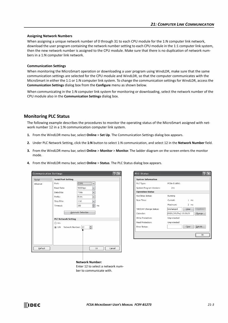
21: COMPUTER LINK COMMUNICATION
Assigning Network Numbers
When assigning a unique network number of 0 through 31 to each CPU module for the 1:N computer link network, download the user program containing the network number setting to each CPU module in the 1:1 computer link system, then the new network number is assigned to the CPU module. Make sure that there is no duplication of network num‐bers in a 1:N computer link network.
Communication Settings
When monitoring the MicroSmart operation or downloading a user program using WindLDR, make sure that the same communication settings are selected for the CPU module and WindLDR, so that the computer communicates with the MicroSmart in either the 1:1 or 1:N computer link system. To change the communication settings for WindLDR, access the Communication Settings dialog box from the Configure menu as shown below.
When communicating in the 1:N computer link system for monitoring or downloading, select the network number of the CPU module also in the Communication Settings dialog box.
Monitoring PLC StatusThe following example describes the procedures to monitor the operating status of the MicroSmart assigned with net‐work number 12 in a 1:N communication computer link system.
1. From the WindLDR menu bar, select Online > Set Up. The Communication Settings dialog box appears.
2. Under PLC Network Setting, click the 1:N button to select 1:N communication, and select 12 in the Network Number field.
3. From the WindLDR menu bar, select Online > Monitor > Monitor. The ladder diagram on the screen enters the monitor mode.
4. From the WindLDR menu bar, select Online > Status. The PLC Status dialog box appears.
Network Number:Enter 12 to select a network num‐ber to communicate with.
FC5A MICROSMART USER’S MANUAL FC9Y‐B1273 21‐3

21: COMPUTER LINK COMMUNICATION
21‐4 FC5A MICROSMART USER’S MANUAL FC9Y‐B1273
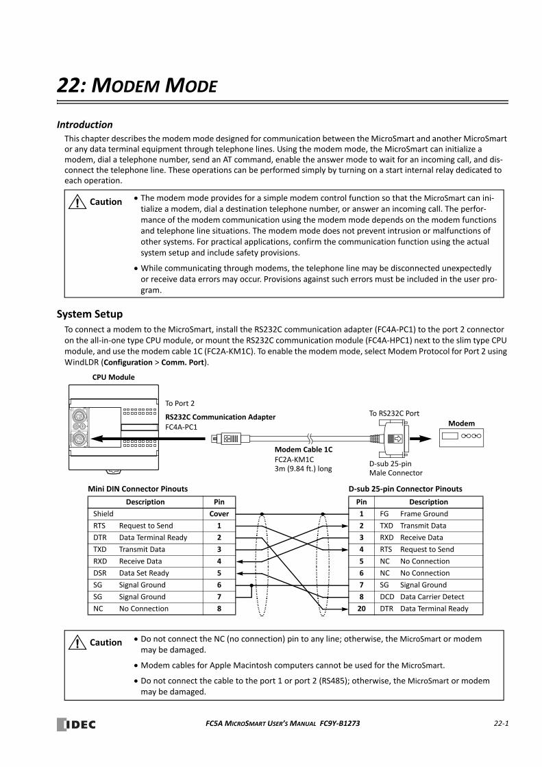
22: MODEM MODE
Introduction This chapter describes the modem mode designed for communication between the MicroSmart and another MicroSmart or any data terminal equipment through telephone lines. Using the modem mode, the MicroSmart can initialize a modem, dial a telephone number, send an AT command, enable the answer mode to wait for an incoming call, and dis‐connect the telephone line. These operations can be performed simply by turning on a start internal relay dedicated to each operation.
System SetupTo connect a modem to the MicroSmart, install the RS232C communication adapter (FC4A‐PC1) to the port 2 connector on the all‐in‐one type CPU module, or mount the RS232C communication module (FC4A‐HPC1) next to the slim type CPU module, and use the modem cable 1C (FC2A‐KM1C). To enable the modem mode, select Modem Protocol for Port 2 using WindLDR (Configuration > Comm. Port).
Caution The modem mode provides for a simple modem control function so that the MicroSmart can ini‐tialize a modem, dial a destination telephone number, or answer an incoming call. The perfor‐mance of the modem communication using the modem mode depends on the modem functions and telephone line situations. The modem mode does not prevent intrusion or malfunctions of other systems. For practical applications, confirm the communication function using the actual system setup and include safety provisions.
While communicating through modems, the telephone line may be disconnected unexpectedly or receive data errors may occur. Provisions against such errors must be included in the user pro‐gram.
Modem Cable 1CFC2A‐KM1C3m (9.84 ft.) long
To RS232C Port
D‐sub 25‐pinMale Connector
D‐sub 25‐pin Connector Pinouts
Pin Description
1 FG Frame Ground
2 TXD Transmit Data
3 RXD Receive Data
4 RTS Request to Send
5 NC No Connection
6 NC No Connection
7 SG Signal Ground
8 DCD Data Carrier Detect
20 DTR Data Terminal Ready
Modem
Mini DIN Connector Pinouts
Description Pin
Shield Cover
RTS Request to Send 1
DTR Data Terminal Ready 2
TXD Transmit Data 3
RXD Receive Data 4
DSR Data Set Ready 5
SG Signal Ground 6
SG Signal Ground 7
NC No Connection 8
Caution Do not connect the NC (no connection) pin to any line; otherwise, the MicroSmart or modem may be damaged.
Modem cables for Apple Macintosh computers cannot be used for the MicroSmart.
Do not connect the cable to the port 1 or port 2 (RS485); otherwise, the MicroSmart or modem may be damaged.
To Port 2
RS232C Communication AdapterFC4A‐PC1
CPU Module
FC5A MICROSMART USER’S MANUAL FC9Y‐B1273 22‐1
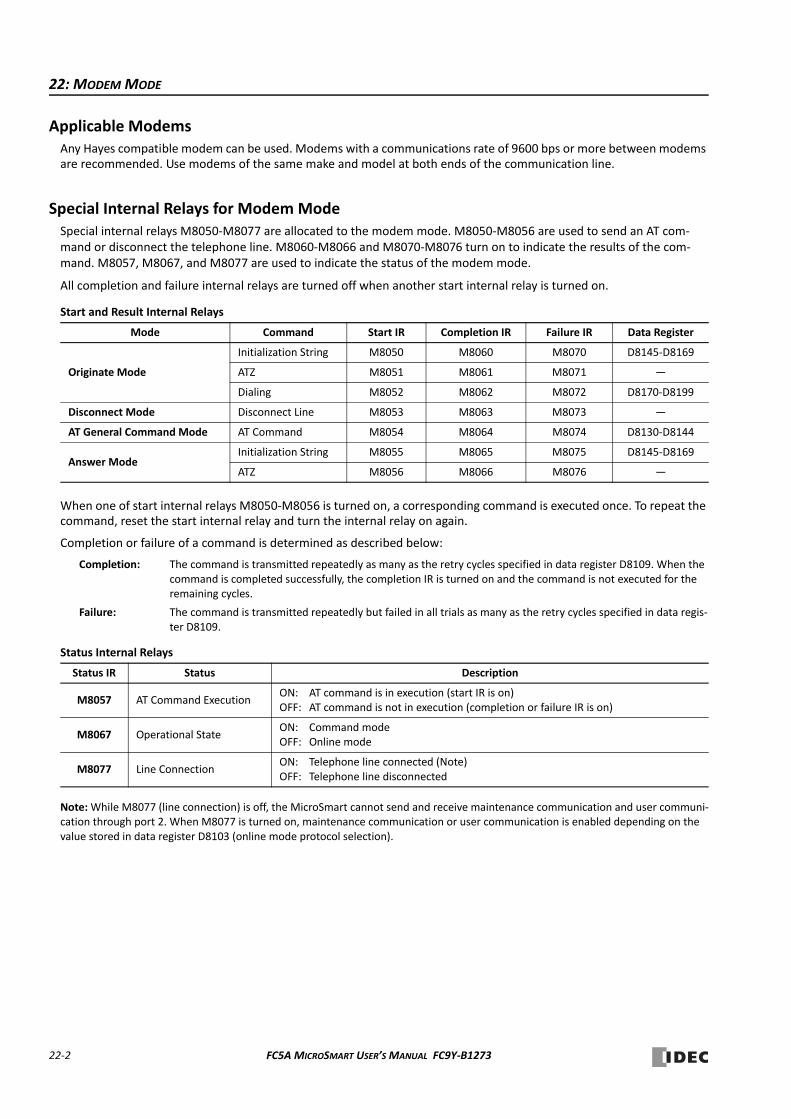
22: MODEM MODE
Applicable ModemsAny Hayes compatible modem can be used. Modems with a communications rate of 9600 bps or more between modems are recommended. Use modems of the same make and model at both ends of the communication line.
Special Internal Relays for Modem ModeSpecial internal relays M8050‐M8077 are allocated to the modem mode. M8050‐M8056 are used to send an AT com‐mand or disconnect the telephone line. M8060‐M8066 and M8070‐M8076 turn on to indicate the results of the com‐mand. M8057, M8067, and M8077 are used to indicate the status of the modem mode.
All completion and failure internal relays are turned off when another start internal relay is turned on.
Start and Result Internal Relays
When one of start internal relays M8050‐M8056 is turned on, a corresponding command is executed once. To repeat the command, reset the start internal relay and turn the internal relay on again.
Completion or failure of a command is determined as described below:
Completion: The command is transmitted repeatedly as many as the retry cycles specified in data register D8109. When the command is completed successfully, the completion IR is turned on and the command is not executed for the remaining cycles.
Failure: The command is transmitted repeatedly but failed in all trials as many as the retry cycles specified in data regis‐ter D8109.
Status Internal Relays
Note: While M8077 (line connection) is off, the MicroSmart cannot send and receive maintenance communication and user communi‐cation through port 2. When M8077 is turned on, maintenance communication or user communication is enabled depending on the value stored in data register D8103 (online mode protocol selection).
Mode Command Start IR Completion IR Failure IR Data Register
Originate Mode
Initialization String M8050 M8060 M8070 D8145‐D8169
ATZ M8051 M8061 M8071 —
Dialing M8052 M8062 M8072 D8170‐D8199
Disconnect Mode Disconnect Line M8053 M8063 M8073 —
AT General Command Mode AT Command M8054 M8064 M8074 D8130‐D8144
Answer ModeInitialization String M8055 M8065 M8075 D8145‐D8169
ATZ M8056 M8066 M8076 —
Status IR Status Description
M8057 AT Command ExecutionON: AT command is in execution (start IR is on)OFF: AT command is not in execution (completion or failure IR is on)
M8067 Operational StateON: Command modeOFF: Online mode
M8077 Line ConnectionON: Telephone line connected (Note)OFF: Telephone line disconnected
22‐2 FC5A MICROSMART USER’S MANUAL FC9Y‐B1273
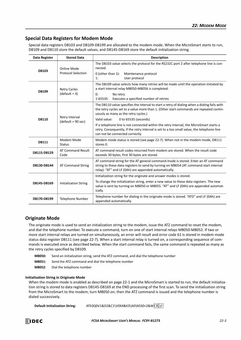
22: MODEM MODE
Special Data Registers for Modem ModeSpecial data registers D8103 and D8109‐D8199 are allocated to the modem mode. When the MicroSmart starts to run, D8109 and D8110 store the default values, and D8145‐D8169 store the default initialization string.
Originate ModeThe originate mode is used to send an initialization string to the modem, issue the ATZ command to reset the modem, and dial the telephone number. To execute a command, turn on one of start internal relays M8050‐M8052. If two or more start internal relays are turned on simultaneously, an error will result and error code 61 is stored in modem mode status data register D8111 (see page 22‐7). When a start internal relay is turned on, a corresponding sequence of com‐mands is executed once as described below. When the start command fails, the same command is repeated as many as the retry cycles specified by D8109.
M8050: Send an initialization string, send the ATZ command, and dial the telephone number
M8051: Send the ATZ command and dial the telephone number
M8052: Dial the telephone number
Initialization String in Originate ModeWhen the modem mode is enabled as described on page 22‐1 and the MicroSmart is started to run, the default initializa‐tion string is stored to data registers D8145‐D8169 at the END processing of the first scan. To send the initialization string from the MicroSmart to the modem, turn M8050 on; then the ATZ command is issued and the telephone number is dialed successively.
Default Initialization String: ATE0Q0V1&D2&C1\V0X4&K3\A0\N5S0=2&W
Data Register Stored Data Description
D8103Online Mode Protocol Selection
The D8103 value selects the protocol for the RS232C port 2 after telephone line is con‐nected.
0 (other than 1): Maintenance protocol1: User protocol
D8109Retry Cycles(default = 3)
The D8109 value selects how many retries will be made until the operation initiated by a start internal relay M8050‐M8056 is completed.
0: No retry1‐65535: Executes a specified number of retries
D8110Retry Interval(default = 90 sec)
The D8110 value specifies the interval to start a retry of dialing when a dialing fails with the retry cycles set to a value more than 1. (Other start commands are repeated contin‐uously as many as the retry cycles.)
Valid value: 0 to 65535 (seconds)
If a telephone line is not connected within the retry interval, the MicroSmart starts a retry. Consequently, if the retry interval is set to a too small value, the telephone line can not be connected correctly.
D8111Modem Mode Status
Modem mode status is stored (see page 22‐7). When not in the modem mode, D8111 stores 0.
D8115‐D8129AT Command Result Code
AT command result codes returned from modem are stored. When the result code exceeds 30 bytes, first 30 bytes are stored.
D8130‐D8144 AT Command StringAT command string for the AT general command mode is stored. Enter an AT command string to these data registers to send by turning on M8054 (AT command start internal relay). “AT” and LF (0Ah) are appended automatically.
D8145‐D8169 Initialization String
Initialization string for the originate and answer modes is stored.
To change the initialization string, enter a new value to these data registers. The new value is sent by turning on M8050 or M8055. “AT” and LF (0Ah) are appended automat‐ically.
D8170‐D8199 Telephone NumberTelephone number for dialing in the originate mode is stored. “ATD” and LF (0Ah) are appended automatically.
CR LF
FC5A MICROSMART USER’S MANUAL FC9Y‐B1273 22‐3
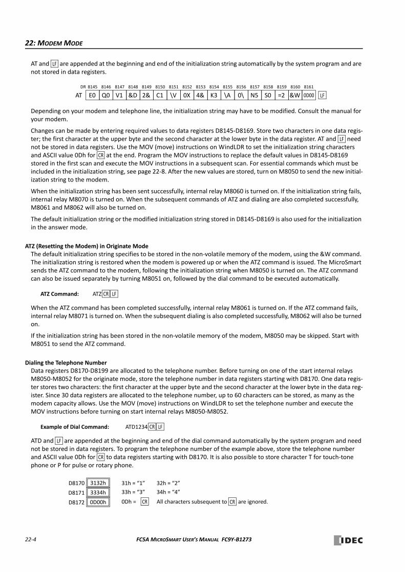
22: MODEM MODE
AT and are appended at the beginning and end of the initialization string automatically by the system program and are not stored in data registers.
Depending on your modem and telephone line, the initialization string may have to be modified. Consult the manual for your modem.
Changes can be made by entering required values to data registers D8145‐D8169. Store two characters in one data regis‐ter; the first character at the upper byte and the second character at the lower byte in the data register. AT and need not be stored in data registers. Use the MOV (move) instructions on WindLDR to set the initialization string characters and ASCII value 0Dh for at the end. Program the MOV instructions to replace the default values in D8145‐D8169 stored in the first scan and execute the MOV instructions in a subsequent scan. For essential commands which must be included in the initialization string, see page 22‐8. After the new values are stored, turn on M8050 to send the new initial‐ization string to the modem.
When the initialization string has been sent successfully, internal relay M8060 is turned on. If the initialization string fails, internal relay M8070 is turned on. When the subsequent commands of ATZ and dialing are also completed successfully, M8061 and M8062 will also be turned on.
The default initialization string or the modified initialization string stored in D8145‐D8169 is also used for the initialization in the answer mode.
ATZ (Resetting the Modem) in Originate ModeThe default initialization string specifies to be stored in the non‐volatile memory of the modem, using the &W command. The initialization string is restored when the modem is powered up or when the ATZ command is issued. The MicroSmart sends the ATZ command to the modem, following the initialization string when M8050 is turned on. The ATZ command can also be issued separately by turning M8051 on, followed by the dial command to be executed automatically.
ATZ Command: ATZ
When the ATZ command has been completed successfully, internal relay M8061 is turned on. If the ATZ command fails, internal relay M8071 is turned on. When the subsequent dialing is also completed successfully, M8062 will also be turned on.
If the initialization string has been stored in the non‐volatile memory of the modem, M8050 may be skipped. Start with M8051 to send the ATZ command.
Dialing the Telephone NumberData registers D8170‐D8199 are allocated to the telephone number. Before turning on one of the start internal relays M8050‐M8052 for the originate mode, store the telephone number in data registers starting with D8170. One data regis‐ter stores two characters: the first character at the upper byte and the second character at the lower byte in the data reg‐ister. Since 30 data registers are allocated to the telephone number, up to 60 characters can be stored, as many as the modem capacity allows. Use the MOV (move) instructions on WindLDR to set the telephone number and execute the MOV instructions before turning on start internal relays M8050‐M8052.
Example of Dial Command: ATD1234
ATD and are appended at the beginning and end of the dial command automatically by the system program and need not be stored in data registers. To program the telephone number of the example above, store the telephone number and ASCII value 0Dh for to data registers starting with D8170. It is also possible to store character T for touch‐tone phone or P for pulse or rotary phone.
LF
0D00
8161
Q0
8146
V1
8147
&D
8148
2&
8149
C1
8150
\V
8151
0X
8152
4&
8153
K3
8154
\A
8155
0\
8156
N5
8157
S0
8158
=2
8159
&W
8160
E0
8145
AT
DR
LF
LF
CR
CR LF
CR LF
LF
CR
3132hD8170
3334hD8171
0D00hD8172
31h = “1” 32h = “2”
33h = “3” 34h = “4”
0Dh = All characters subsequent to CR are ignored.CR
22‐4 FC5A MICROSMART USER’S MANUAL FC9Y‐B1273
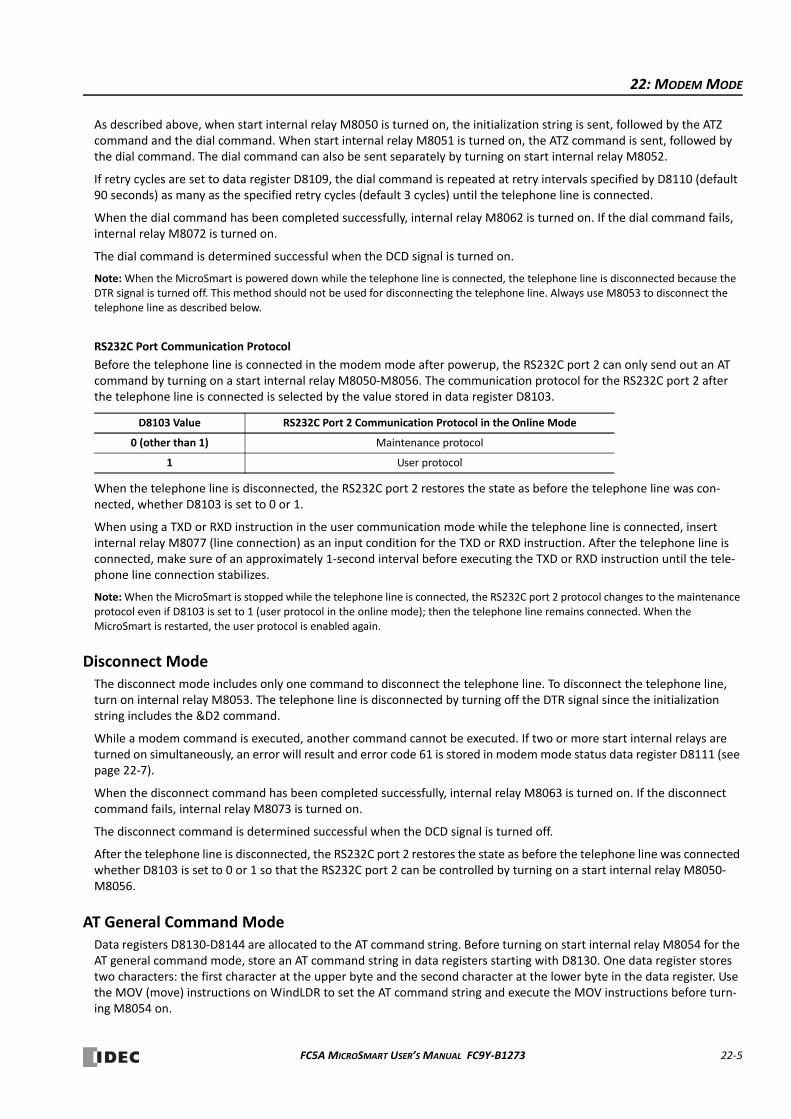
22: MODEM MODE
As described above, when start internal relay M8050 is turned on, the initialization string is sent, followed by the ATZ command and the dial command. When start internal relay M8051 is turned on, the ATZ command is sent, followed by the dial command. The dial command can also be sent separately by turning on start internal relay M8052.
If retry cycles are set to data register D8109, the dial command is repeated at retry intervals specified by D8110 (default 90 seconds) as many as the specified retry cycles (default 3 cycles) until the telephone line is connected.
When the dial command has been completed successfully, internal relay M8062 is turned on. If the dial command fails, internal relay M8072 is turned on.
The dial command is determined successful when the DCD signal is turned on.
Note: When the MicroSmart is powered down while the telephone line is connected, the telephone line is disconnected because the DTR signal is turned off. This method should not be used for disconnecting the telephone line. Always use M8053 to disconnect the telephone line as described below.
RS232C Port Communication Protocol
Before the telephone line is connected in the modem mode after powerup, the RS232C port 2 can only send out an AT command by turning on a start internal relay M8050‐M8056. The communication protocol for the RS232C port 2 after the telephone line is connected is selected by the value stored in data register D8103.
When the telephone line is disconnected, the RS232C port 2 restores the state as before the telephone line was con‐nected, whether D8103 is set to 0 or 1.
When using a TXD or RXD instruction in the user communication mode while the telephone line is connected, insert internal relay M8077 (line connection) as an input condition for the TXD or RXD instruction. After the telephone line is connected, make sure of an approximately 1‐second interval before executing the TXD or RXD instruction until the tele‐phone line connection stabilizes.
Note: When the MicroSmart is stopped while the telephone line is connected, the RS232C port 2 protocol changes to the maintenance protocol even if D8103 is set to 1 (user protocol in the online mode); then the telephone line remains connected. When the MicroSmart is restarted, the user protocol is enabled again.
Disconnect ModeThe disconnect mode includes only one command to disconnect the telephone line. To disconnect the telephone line, turn on internal relay M8053. The telephone line is disconnected by turning off the DTR signal since the initialization string includes the &D2 command.
While a modem command is executed, another command cannot be executed. If two or more start internal relays are turned on simultaneously, an error will result and error code 61 is stored in modem mode status data register D8111 (see page 22‐7).
When the disconnect command has been completed successfully, internal relay M8063 is turned on. If the disconnect command fails, internal relay M8073 is turned on.
The disconnect command is determined successful when the DCD signal is turned off.
After the telephone line is disconnected, the RS232C port 2 restores the state as before the telephone line was connected whether D8103 is set to 0 or 1 so that the RS232C port 2 can be controlled by turning on a start internal relay M8050‐M8056.
AT General Command ModeData registers D8130‐D8144 are allocated to the AT command string. Before turning on start internal relay M8054 for the AT general command mode, store an AT command string in data registers starting with D8130. One data register stores two characters: the first character at the upper byte and the second character at the lower byte in the data register. Use the MOV (move) instructions on WindLDR to set the AT command string and execute the MOV instructions before turn‐ing M8054 on.
D8103 Value RS232C Port 2 Communication Protocol in the Online Mode
0 (other than 1) Maintenance protocol
1 User protocol
FC5A MICROSMART USER’S MANUAL FC9Y‐B1273 22‐5
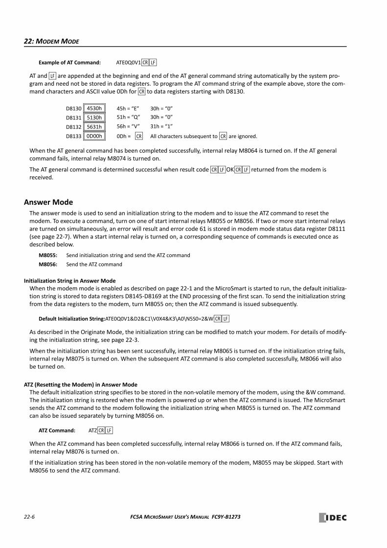
22: MODEM MODE
Example of AT Command: ATE0Q0V1
AT and are appended at the beginning and end of the AT general command string automatically by the system pro‐gram and need not be stored in data registers. To program the AT command string of the example above, store the com‐mand characters and ASCII value 0Dh for to data registers starting with D8130.
When the AT general command has been completed successfully, internal relay M8064 is turned on. If the AT general command fails, internal relay M8074 is turned on.
The AT general command is determined successful when result code OK returned from the modem is received.
Answer ModeThe answer mode is used to send an initialization string to the modem and to issue the ATZ command to reset the modem. To execute a command, turn on one of start internal relays M8055 or M8056. If two or more start internal relays are turned on simultaneously, an error will result and error code 61 is stored in modem mode status data register D8111 (see page 22‐7). When a start internal relay is turned on, a corresponding sequence of commands is executed once as described below.
M8055: Send initialization string and send the ATZ command
M8056: Send the ATZ command
Initialization String in Answer ModeWhen the modem mode is enabled as described on page 22‐1 and the MicroSmart is started to run, the default initializa‐tion string is stored to data registers D8145‐D8169 at the END processing of the first scan. To send the initialization string from the data registers to the modem, turn M8055 on; then the ATZ command is issued subsequently.
Default Initialization String:ATE0Q0V1&D2&C1\V0X4&K3\A0\N5S0=2&W
As described in the Originate Mode, the initialization string can be modified to match your modem. For details of modify‐ing the initialization string, see page 22‐3.
When the initialization string has been sent successfully, internal relay M8065 is turned on. If the initialization string fails, internal relay M8075 is turned on. When the subsequent ATZ command is also completed successfully, M8066 will also be turned on.
ATZ (Resetting the Modem) in Answer ModeThe default initialization string specifies to be stored in the non‐volatile memory of the modem, using the &W command. The initialization string is restored when the modem is powered up or when the ATZ command is issued. The MicroSmart sends the ATZ command to the modem following the initialization string when M8055 is turned on. The ATZ command can also be issued separately by turning M8056 on.
ATZ Command: ATZ
When the ATZ command has been completed successfully, internal relay M8066 is turned on. If the ATZ command fails, internal relay M8076 is turned on.
If the initialization string has been stored in the non‐volatile memory of the modem, M8055 may be skipped. Start with M8056 to send the ATZ command.
CR LF
LF
CR
4530hD8130
5130hD8131
5631hD8132
45h = “E” 30h = “0”
51h = “Q” 30h = “0”
56h = “V” 31h = “1”
0D00hD8133 0Dh = All characters subsequent to CR are ignored.CR
CR LF CR LF
CR LF
CR LF
22‐6 FC5A MICROSMART USER’S MANUAL FC9Y‐B1273
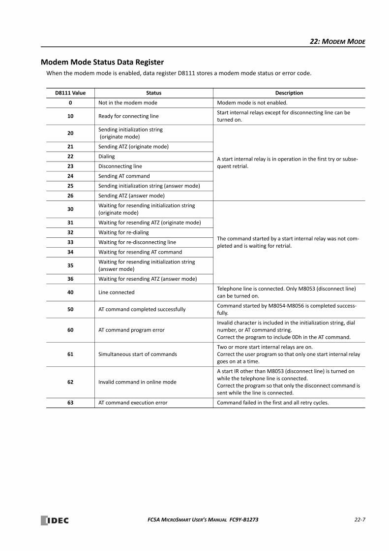
22: MODEM MODE
Modem Mode Status Data RegisterWhen the modem mode is enabled, data register D8111 stores a modem mode status or error code.
D8111 Value Status Description
0 Not in the modem mode Modem mode is not enabled.
10 Ready for connecting lineStart internal relays except for disconnecting line can be turned on.
20Sending initialization string (originate mode)
A start internal relay is in operation in the first try or subse‐quent retrial.
21 Sending ATZ (originate mode)
22 Dialing
23 Disconnecting line
24 Sending AT command
25 Sending initialization string (answer mode)
26 Sending ATZ (answer mode)
30Waiting for resending initialization string(originate mode)
The command started by a start internal relay was not com‐pleted and is waiting for retrial.
31 Waiting for resending ATZ (originate mode)
32 Waiting for re‐dialing
33 Waiting for re‐disconnecting line
34 Waiting for resending AT command
35Waiting for resending initialization string(answer mode)
36 Waiting for resending ATZ (answer mode)
40 Line connectedTelephone line is connected. Only M8053 (disconnect line) can be turned on.
50 AT command completed successfullyCommand started by M8054‐M8056 is completed success‐fully.
60 AT command program errorInvalid character is included in the initialization string, dial number, or AT command string. Correct the program to include 0Dh in the AT command.
61 Simultaneous start of commandsTwo or more start internal relays are on. Correct the user program so that only one start internal relay goes on at a time.
62 Invalid command in online mode
A start IR other than M8053 (disconnect line) is turned on while the telephone line is connected. Correct the program so that only the disconnect command is sent while the line is connected.
63 AT command execution error Command failed in the first and all retry cycles.
FC5A MICROSMART USER’S MANUAL FC9Y‐B1273 22‐7
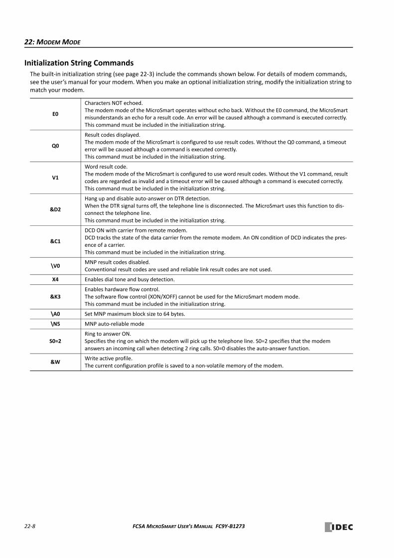
22: MODEM MODE
Initialization String CommandsThe built‐in initialization string (see page 22‐3) include the commands shown below. For details of modem commands, see the user’s manual for your modem. When you make an optional initialization string, modify the initialization string to match your modem.
E0
Characters NOT echoed.The modem mode of the MicroSmart operates without echo back. Without the E0 command, the MicroSmart misunderstands an echo for a result code. An error will be caused although a command is executed correctly.This command must be included in the initialization string.
Q0
Result codes displayed.The modem mode of the MicroSmart is configured to use result codes. Without the Q0 command, a timeout error will be caused although a command is executed correctly.This command must be included in the initialization string.
V1
Word result code.The modem mode of the MicroSmart is configured to use word result codes. Without the V1 command, result codes are regarded as invalid and a timeout error will be caused although a command is executed correctly.This command must be included in the initialization string.
&D2
Hang up and disable auto‐answer on DTR detection.When the DTR signal turns off, the telephone line is disconnected. The MicroSmart uses this function to dis‐connect the telephone line.This command must be included in the initialization string.
&C1
DCD ON with carrier from remote modem.DCD tracks the state of the data carrier from the remote modem. An ON condition of DCD indicates the pres‐ence of a carrier.This command must be included in the initialization string.
\V0MNP result codes disabled.Conventional result codes are used and reliable link result codes are not used.
X4 Enables dial tone and busy detection.
&K3Enables hardware flow control. The software flow control (XON/XOFF) cannot be used for the MicroSmart modem mode.This command must be included in the initialization string.
\A0 Set MNP maximum block size to 64 bytes.
\N5 MNP auto‐reliable mode
S0=2Ring to answer ON.Specifies the ring on which the modem will pick up the telephone line. S0=2 specifies that the modem answers an incoming call when detecting 2 ring calls. S0=0 disables the auto‐answer function.
&WWrite active profile.The current configuration profile is saved to a non‐volatile memory of the modem.
22‐8 FC5A MICROSMART USER’S MANUAL FC9Y‐B1273
22: MODEM MODE
Preparations for Using ModemBefore using a modem, read the user’s manual for your modem.
The required initialization string depends on the model and make of the modem. When the MicroSmart starts to run the user program, the default modem initialization strings is stored to D8145‐D8169. See page 22‐3.
Default Initialization String: ATE0Q0V1&D2&C1\V0X4&K3\A0\N5S0=2&W
Programming Data Registers and Internal RelaysTo enable the modem mode and communicate through the telephone line, the following settings are needed.
1. If the default initialization string does not match your modem, program a proper initialization string and enter the ASCII val‐ues to data registers starting with D8145 (initialization string). To send out the new initialization string, turn on internal relay M8050 (initialization string start IR) after the new values have been stored to the data registers.
2. Program to move 0 or 1 to data register D8103 (online mode protocol selection) to select maintenance protocol or user pro‐tocol for the RS232C port 2 after telephone line is connected.
3. Program the destination telephone number if dialing is required. Enter the ASCII values of the telephone number to data registers starting with D8170 (telephone number). Store two characters each in one data register. Enter 0Dh at the end of the telephone number. See page 22‐4.
4. If you want to change the default value of 3 retry cycles, program to move a required value to data register D8109.
5. Include internal relays M8050‐M8077 in the user program to control the modem communication as required.
Setting Up the CPU Module
1. Install the RS232C communication adapter (FC4A‐PC1) to the port 2 connector on the all‐in‐one type CPU module.
When using any slim type CPU module, mount the RS232C communication module (FC4A‐HPC1) next to the slim type CPU module, and use the port 2 on the RS232C communication module.
When using the HMI base module with any slim type CPU module, install the RS232C communication adapter (FC4A‐PC1) to the port 2 connector on the HMI base module.
2. Connect the MicroSmart CPU module port 2 to a modem using the modem cable 1C (FC2A‐KM1C) as shown on page 22‐1.
CR LF
FC5A MICROSMART USER’S MANUAL FC9Y‐B1273 22‐9

22: MODEM MODE
Programming WindLDRThe Communication page in the Function Area Settings must be programmed to enable the modem communication for port 2. If required, communication parameters of the CPU module port 2 can also be changed.
Since these settings relate to the user program, the user program must be downloaded to the MicroSmart after changing any of these settings.
1. From the WindLDR menu bar, select Configuration > Comm Ports.
The Function Area Settings dialog box for Communication Ports appears.
2. In the Communication Mode pull‐down list for Port 2, select Modem Protocol.
3. Click the Configure button. The Communication Parameters dialog box appears. Change settings, if required.
The default communication parameters shown below are recommended.
4. Click the OK button.
Baud rate 9600 bps Only when the modem connected on the communication line uses differ‐ent communication parameters than the default values of the MicroSmart, set the matching communication parameters. Since the total of modem communication parameters is 10 bits, set the value to a total of 10 bits.
Start bit 1Data bits 7Parity EvenStop bit 1
Total 10 bits
Baud Rate (bps)1200, 2400, 4800, 9600, 19200,38400, 57600
Data Bits 7 or 8
Parity Even, Odd, None
Stop Bits 1 or 2
Receive Timeout (ms)10 to 2540 (10‐ms increments)(Receive timeout is disabled when 2550 is selected.)
Network Number 0 to 31
22‐10 FC5A MICROSMART USER’S MANUAL FC9Y‐B1273
22: MODEM MODE
Operating Procedure for Modem Mode
1. After completing the user program including the Function Area Settings, download the user program to the MicroSmart from a computer running WindLDR.
2. Start the MicroSmart to run the user program.
3. Turn on start internal relay M8050 or M8055 to initialize the modem.
When originating the modem communication, turn on M8050 to send the initialization string, the ATZ command, and the dial command. If the initialization string has been stored in the non‐volatile memory of the modem, turn on M8051 to start with the ATZ command followed by the dial command.
When answering an incoming call, turn on M8055 to send the initialization string and the ATZ command. If the initialization string has been stored in the non‐volatile memory of the modem, turn on M8056 to send the ATZ command only.
4. Transmit or receive communication through the modem.
5. Turn on start internal relay M8053 to disconnect the telephone line.
FC5A MICROSMART USER’S MANUAL FC9Y‐B1273 22‐11

22: MODEM MODE
Sample Program for Modem Originate ModeThis program demonstrates a user program for the modem originate mode to move values to data registers assigned to the modem mode, initialize the modem, dial the telephone number, and disconnect the telephone line. While the tele‐phone line is connected, user communication instruction TXD2 sends a character string “Connect.”
The TXD2 instruction in the sample program for the modem originate mode is programmed using WindLDR with parame‐ters shown below:
M8120 is the initialize pulse special internal relay.
The MOV instruction stores 1 to D8103 to enable user protocol after telephone line is connected.
MOV instructions set a dial command ATD1234 .
“12” (3132h = 12594) D8170
“34” (3334h = 13108) D8171
“CR” (0D00h = 3328) D8172 to enter at the end of the telephone number.
When input I0 is turned on, M8050 (initialization string) is turned on to send the initialization string, ATZ, and dial com‐mand to the modem.
M8077 (line connection status) is on while telephone line is connected.
When I1 is turned on, TXD2 sends seven characters “Connect.” See the WindLDR dialog box shown below.
When input I2 is turned on, M8053 (disconnect line) is turned on to disconnect the telephone line.
CR LF
CR
M8120
REPS1 –1
D1 –D8103
MOV(W)
I0
I1 M8077SOTU D2
D0S17
D1M0
TXD2
I2
M8050
M8053
M8120
REPS1 –12594
D1 –D8170
MOV(W)
REPS1 –13108
D1 –D8171
MOV(W)
REPS1 –3328
D1 –D8172
MOV(W)
22‐12 FC5A MICROSMART USER’S MANUAL FC9Y‐B1273
22: MODEM MODE
Sample Program for Modem Answer ModeThis program demonstrates a user program for the modem answer mode to move a value to a data register assigned to the modem mode and initialize the modem. While the telephone line is connected, user communication instruction RXD2 is executed to receive an incoming communication.
The RXD2 instruction is programmed using WindLDR with parameters shown below:
Source S1: Data register D10, No conversion, 2 digits, Repeat 10
M8120 is the initialize pulse special internal relay.
When the MicroSmart starts to run, M8055 is turned on to send the ini‐tialization string for the modem answer mode.
The MOV instruction stores 1 to D8103 to enable user protocol after telephone line is connected.
M8077 (line connection status) is on while telephone line is connected.
RXD2 receives incoming communication and stores received data to data registers starting with D10.
M8120
M8120
REPS1 –1
D1 –D8103
MOV(W)
M8077
D2D0
S120
D1M0
RXD2
M8055
FC5A MICROSMART USER’S MANUAL FC9Y‐B1273 22‐13
22: MODEM MODE
Troubleshooting in Modem Communication
When a start internal relay is turned on, the data of D8111 (modem mode status) changes, but the modem does not work.
Cause: A wrong cable is used or wiring is incorrect.
Solution: Use the modem cable 1C (FC2A‐KM1C).
The DTR or ER indicator on the modem does not turn on.
Cause: A wrong cable is used or wiring is incorrect.
Solution: Use the modem cable 1C (FC2A‐KM1C).
When a start internal relay is turned on, the data of D8111 (modem mode status) does not change.
Cause: Modem protocol is not selected for port 2.
Solution: Select Modem Protocol for Port 2 using WindLDR (Configure > Function Area Settings > Communication) and download the user program to the CPU module.
When an initialization string is sent, a failure occurs, but sending ATZ completes successfully.
Cause: The initialization string is not valid for the modem.
Solution: Refer to the user’s manual for the modem and correct the initialization string.
When a dial command is sent, a result code “NO DIALTONE” is returned and the telephone line is not connected.
Cause 1: The modular cable is not connected.
Solution 1: Connect the modular cable to the modem.
Cause 2: The modem is used in a PBX environment.
Solution 2: Add X0 or X3 to the initialization string stored in data registers D8145‐D8169, and try initialization again.
Dialing completes successfully, but the telephone line is disconnected in a short period of time.
Cause 1: The modem settings at the both ends of the line are different.
Solution 1: Make the same settings for the modems at the both ends.
Cause 2: The model of the modems at the both ends of the line is different.
Solution 2: Use the same modems at the both ends.
Cause 3: The quality of the telephone line is low.
Solution 3: Decrease the baud rate of the MicroSmart to lower than 9600 bps.
22‐14 FC5A MICROSMART USER’S MANUAL FC9Y‐B1273
23: MODBUS TCP COMMUNICATION
IntroductionThis chapter describes the Modbus TCP master (client) and slave (server) communication function of the FC5A MicroSmart CPU module.
All FC5A MicroSmart CPU modules with system program ver. 210 or higher can use the Modbus TCP communication to send and receive data with Modbus devices through the Ethernet line.
Modbus TCP Communication General InformationWhen connected with the web server module (FC4A‐SX5ES1E), the FC5A MicroSmart CPU module can be used as a mas‐ter (client) or a slave (server) of the Modbus TCP communication.
Using the Modbus TCP master communication, the CPU module can change or monitor data in Modbus server devises through communication port 2.
In the Modbus TCP slave communication, a Modbus master device can change or monitor device values in the MicroSmart CPU module through communication port 1 or port 2.
Modbus TCP master communication functions and configuration are described on page 23‐2. Modbus TCP slave commu‐nication functions and configuration are described on page 23‐5.
To use the Modbus TCP communication, FC5A MicroSmart CPU modules with system program ver. 210 or higher and WindLDR ver. 5.3 or higher are required. The system program version can be confirmed using WindLDR. See page 13‐1 (Basic Vol.).
When the CPU module system program version is lower than 210, you can download the latest system program using WindLDR ver. 5.1 or higher. See page A‐9 (Basic Vol.).
Applicable CPU Modules All FC5A CPU modules
System Program Version 210 or higher
WindLDR Version 5.3 or higher
FC5A MICROSMART USER’S MANUAL FC9Y‐B1273 23‐1
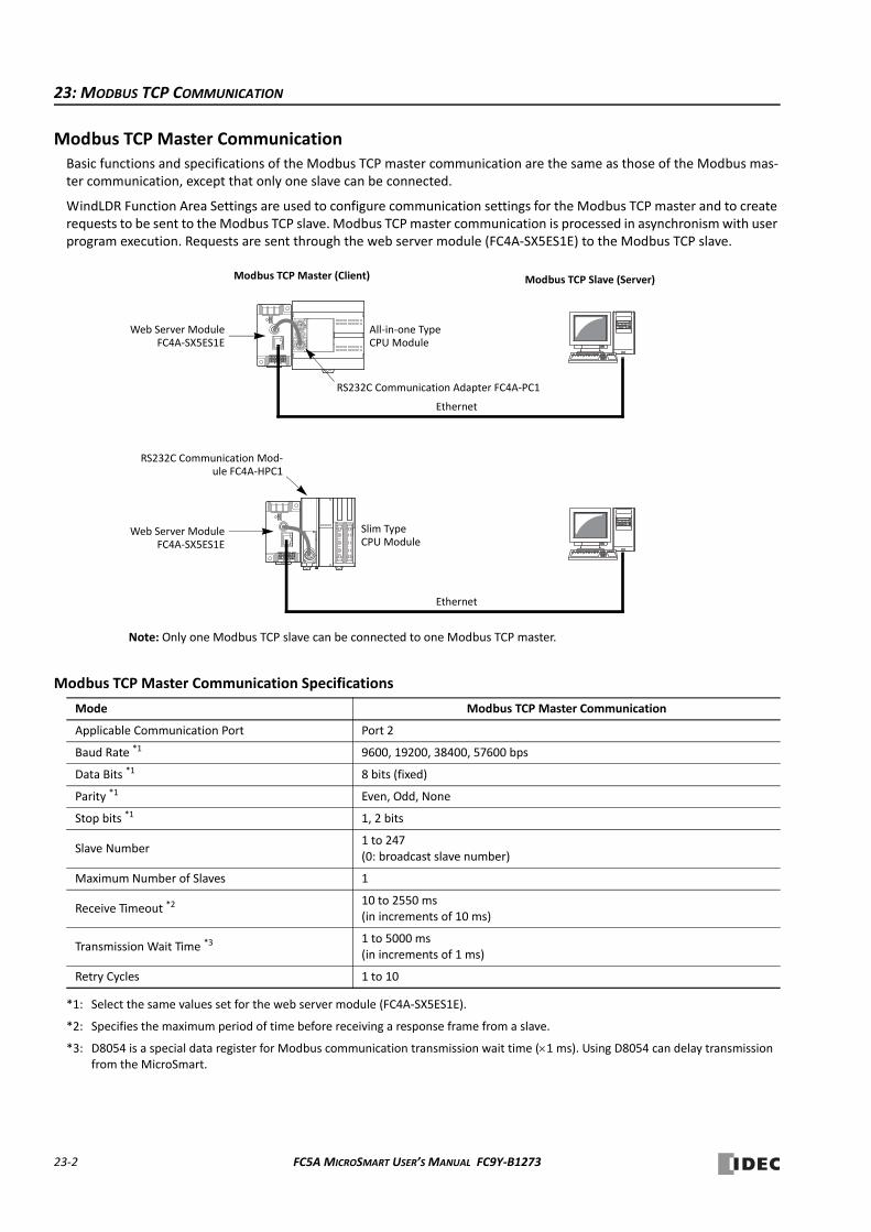
23: MODBUS TCP COMMUNICATION
Modbus TCP Master CommunicationBasic functions and specifications of the Modbus TCP master communication are the same as those of the Modbus mas‐ter communication, except that only one slave can be connected.
WindLDR Function Area Settings are used to configure communication settings for the Modbus TCP master and to create requests to be sent to the Modbus TCP slave. Modbus TCP master communication is processed in asynchronism with user program execution. Requests are sent through the web server module (FC4A‐SX5ES1E) to the Modbus TCP slave.
Modbus TCP Master Communication Specifications
*1: Select the same values set for the web server module (FC4A‐SX5ES1E).
*2: Specifies the maximum period of time before receiving a response frame from a slave.
*3: D8054 is a special data register for Modbus communication transmission wait time (1 ms). Using D8054 can delay transmission from the MicroSmart.
Mode Modbus TCP Master Communication
Applicable Communication Port Port 2
Baud Rate *1 9600, 19200, 38400, 57600 bps
Data Bits *1 8 bits (fixed)
Parity *1 Even, Odd, None
Stop bits *1 1, 2 bits
Slave Number1 to 247(0: broadcast slave number)
Maximum Number of Slaves 1
Receive Timeout *210 to 2550 ms (in increments of 10 ms)
Transmission Wait Time *31 to 5000 ms (in increments of 1 ms)
Retry Cycles 1 to 10
Web Server ModuleFC4A‐SX5ES1E
RS232C Communication Mod‐ule FC4A‐HPC1
Slim Type CPU Module
Ethernet
Web Server ModuleFC4A‐SX5ES1E
All‐in‐one Type CPU Module
Modbus TCP Master (Client) Modbus TCP Slave (Server)
Ethernet
RS232C Communication Adapter FC4A‐PC1
Note: Only one Modbus TCP slave can be connected to one Modbus TCP master.
23‐2 FC5A MICROSMART USER’S MANUAL FC9Y‐B1273
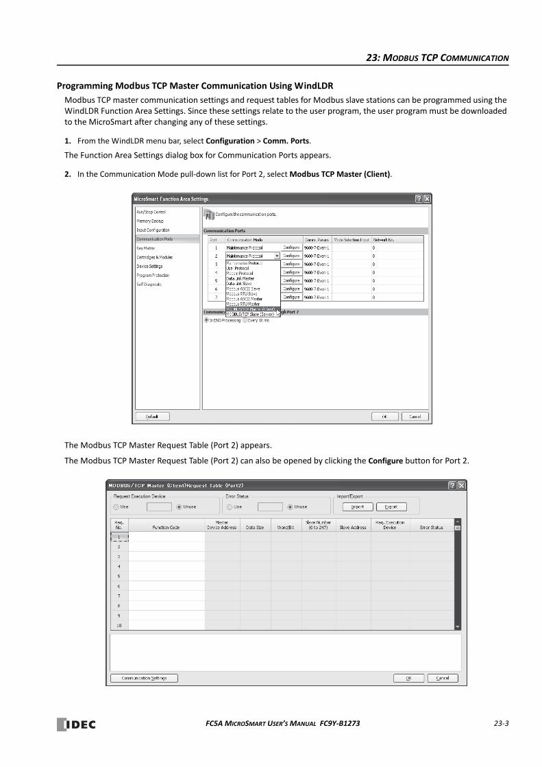
23: MODBUS TCP COMMUNICATION
Programming Modbus TCP Master Communication Using WindLDR
Modbus TCP master communication settings and request tables for Modbus slave stations can be programmed using the WindLDR Function Area Settings. Since these settings relate to the user program, the user program must be downloaded to the MicroSmart after changing any of these settings.
1. From the WindLDR menu bar, select Configuration > Comm. Ports.
The Function Area Settings dialog box for Communication Ports appears.
2. In the Communication Mode pull‐down list for Port 2, select Modbus TCP Master (Client).
The Modbus TCP Master Request Table (Port 2) appears.
The Modbus TCP Master Request Table (Port 2) can also be opened by clicking the Configure button for Port 2.
FC5A MICROSMART USER’S MANUAL FC9Y‐B1273 23‐3

23: MODBUS TCP COMMUNICATION
3. Click the Communication Settings button.
The Communication Settings dialog box appears. Change settings, if required.
4. Click the OK button to return to the Modbus TCP Master Request Table (Port 2). Designate requests under the Function Code. A maximum of 2040 requests can be entered in one request table.
Choose to use Request Execution Device and Error Status data registers. When using Request Execution Device and Error Status data registers, enter the first number of the devices.
Notes for Editing the Request Table
Request execution devices and error status data registers are allocated in the order of request numbers. When deleting a request or changing the order of requests, the relationship of the request to the request execution devices and error status data register is changed. If the internal relay or data register is used in the user program, the device addresses must be changed accordingly. After completing the changes, download the user program again.
5. When editing the Modbus TCP Master Request Table (Port 2) is complete, click the OK button to save changes.
6. Download the user program to the CPU module.
Now, programming for the Modbus TCP master is complete. Parameters and valid values are the same as Modbus master communication. For details, see pages 12‐7 through 12‐9 (Basic Vol.).
*: Select the same values set for the web server module (FC4A‐SX5ES1E).
Baud Rate (bps) * 9600, 19200, 38400, 57600
Parity * Even, Odd, None
Stop Bits * 1 or 2
Retry Cycle 1 to 10
Receive Timeout 1 to 255 (10 ms)
23‐4 FC5A MICROSMART USER’S MANUAL FC9Y‐B1273

23: MODBUS TCP COMMUNICATION
Modbus TCP Slave CommunicationWindLDR Function Area Settings are used to configure communication settings for the Modbus TCP slave communication through communication port 1 or 2 of the MicroSmart CPU module. In the Modbus TCP communication, when the Mod‐bus TCP slave receives a request from the Modbus TCP master, the Modbus TCP slave reads or writes devices according to the request. The request is processed at the END processing of the user program. The web server module (FC4A‐SX5ES1E) is used to set up a Modbus TCP slave.
Web Server ModuleFC4A‐SX5ES1E
RS232C Communication Mod‐ule FC4A‐HPC1
Slim Type CPU Module
Ethernet
Web Server ModuleFC4A‐SX5ES1E
All‐in‐one Type CPU Module
Modbus TCP Master (Client) Modbus TCP Slave (Server)
Ethernet
RS232C Communication Adapter FC4A‐PC1
Note: Only one Modbus TCP slave can be connected to one Modbus TCP master.
FC5A MICROSMART USER’S MANUAL FC9Y‐B1273 23‐5
23: MODBUS TCP COMMUNICATION
Modbus TCP Slave Communication Specifications
*1: Select the values from WindLDR > Function Area Settings > Communication.
*2: Special data register D8054 for Modbus communication transmission wait time (1 ms) is used to set the response time. 0 desig‐nates 1 ms, and 5000 or more designates 5000 ms.
*3: When timeout occurs, the MicroSmart discards the received data and waits for the first frame of the next valid communication.
Communication Completion and Communication Error
Modbus TCP communication finishes when a read or write process is completed successfully or when a communication error occurs. Immediately after a request communication has been completed, Modbus communication completion relay M8080 turns on for 1 scan time. When a communication error occurs, the error code is stored to special data register D8053. The data in D8053 is valid only for the 1 scan time when M8080 is on.
When a communication error occurs, communication error special internal relay M8005 also turns on for 1 scan time immediately after the error.
Mode Modbus TCP Slave (Server) Communication
Applicable Communication Port Port 1 Port 2
Baud Rate *1 9600, 19200, 38400, 57600 bps
Data Bits *1 8 bits (fixed)
Parity *1 Odd, even, none
Stop bits *1 1, 2 bits
Slave Number 1 to 247
Response Time 1.5 ms 1 to 5000 ms (in increments of 1 ms) *2
Receive Timeout *3 10 to 2550 ms (in increments of 10 ms)
Special Internal Relay —M8005: Communication errorM8080: Communication completion relay
Special Data Register —D8053: Error codeD8054: Transmission wait time
(in increments of 1 ms)
Applicable Function Code
01 Read Coil Status02 Read Input Status03 Read Holding Registers04 Read Input Registers05 Force Single Coil06 Preset Single Register15 Force Multiple Coils16 Preset Multiple Registers
23‐6 FC5A MICROSMART USER’S MANUAL FC9Y‐B1273
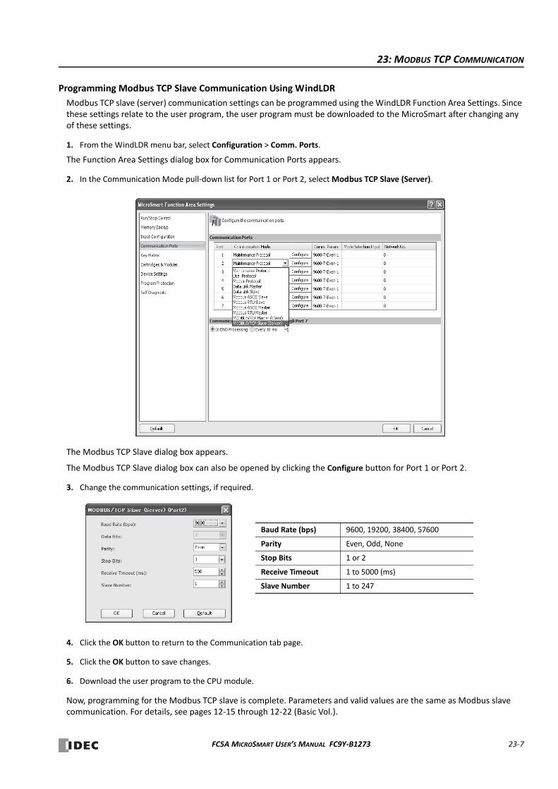
23: MODBUS TCP COMMUNICATION
Programming Modbus TCP Slave Communication Using WindLDR
Modbus TCP slave (server) communication settings can be programmed using the WindLDR Function Area Settings. Since these settings relate to the user program, the user program must be downloaded to the MicroSmart after changing any of these settings.
1. From the WindLDR menu bar, select Configuration > Comm. Ports.
The Function Area Settings dialog box for Communication Ports appears.
2. In the Communication Mode pull‐down list for Port 1 or Port 2, select Modbus TCP Slave (Server).
The Modbus TCP Slave dialog box appears.
The Modbus TCP Slave dialog box can also be opened by clicking the Configure button for Port 1 or Port 2.
3. Change the communication settings, if required.
4. Click the OK button to return to the Communication tab page.
5. Click the OK button to save changes.
6. Download the user program to the CPU module.
Now, programming for the Modbus TCP slave is complete. Parameters and valid values are the same as Modbus slave communication. For details, see pages 12‐15 through 12‐22 (Basic Vol.).
Baud Rate (bps) 9600, 19200, 38400, 57600
Parity Even, Odd, None
Stop Bits 1 or 2
Receive Timeout 1 to 5000 (ms)
Slave Number 1 to 247
FC5A MICROSMART USER’S MANUAL FC9Y‐B1273 23‐7
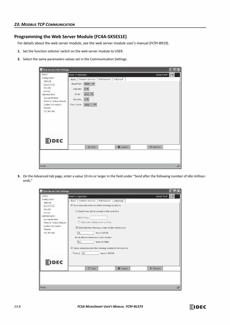
23: MODBUS TCP COMMUNICATION
Programming the Web Server Module (FC4A‐SX5ES1E)For details about the web server module, see the web server module user’s manual (FC9Y‐B919).
1. Set the function selector switch on the web server module to USER.
2. Select the same parameters values set in the Communication Settings.
3. On the Advanced tab page, enter a value 10 ms or larger in the field under “Send after the following number of idle millisec‐onds.”
23‐8 FC5A MICROSMART USER’S MANUAL FC9Y‐B1273
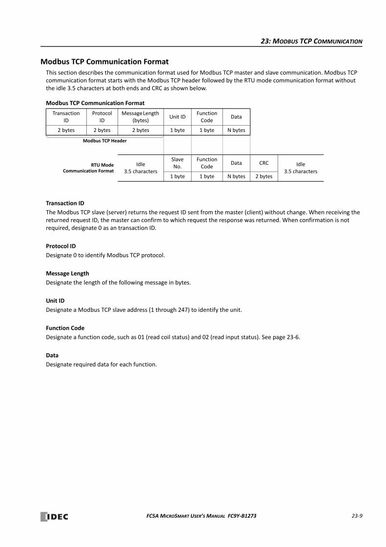
23: MODBUS TCP COMMUNICATION
Modbus TCP Communication FormatThis section describes the communication format used for Modbus TCP master and slave communication. Modbus TCP communication format starts with the Modbus TCP header followed by the RTU mode communication format without the idle 3.5 characters at both ends and CRC as shown below.
Transaction ID
The Modbus TCP slave (server) returns the request ID sent from the master (client) without change. When receiving the returned request ID, the master can confirm to which request the response was returned. When confirmation is not required, designate 0 as an transaction ID.
Protocol ID
Designate 0 to identify Modbus TCP protocol.
Message Length
Designate the length of the following message in bytes.
Unit ID
Designate a Modbus TCP slave address (1 through 247) to identify the unit.
Function Code
Designate a function code, such as 01 (read coil status) and 02 (read input status). See page 23‐6.
Data
Designate required data for each function.
Modbus TCP Communication Format
Transaction ID
Protocol ID
Message Length (bytes)
Unit IDFunction Code
Data
2 bytes 2 bytes 2 bytes 1 byte 1 byte N bytes
RTU ModeCommunication Format
Idle3.5 characters
Slave No.
Function Code
Data CRC Idle3.5 characters
1 byte 1 byte N bytes 2 bytes
Modbus TCP Header
FC5A MICROSMART USER’S MANUAL FC9Y‐B1273 23‐9

23: MODBUS TCP COMMUNICATION
23‐10 FC5A MICROSMART USER’S MANUAL FC9Y‐B1273
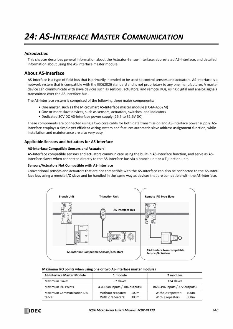
24: AS‐INTERFACE MASTER COMMUNICATION
IntroductionThis chapter describes general information about the Actuator‐Sensor‐Interface, abbreviated AS‐Interface, and detailed information about using the AS‐Interface master module.
About AS‐InterfaceAS‐Interface is a type of field bus that is primarily intended to be used to control sensors and actuators. AS‐Interface is a network system that is compatible with the IEC62026 standard and is not proprietary to any one manufacturer. A master device can communicate with slave devices such as sensors, actuators, and remote I/Os, using digital and analog signals transmitted over the AS‐Interface bus.
The AS‐Interface system is comprised of the following three major components:
One master, such as the MicroSmart AS‐Interface master module (FC4A‐AS62M) One or more slave devices, such as sensors, actuators, switches, and indicators Dedicated 30V DC AS‐Interface power supply (26.5 to 31.6V DC)
These components are connected using a two‐core cable for both data transmission and AS‐Interface power supply. AS‐Interface employs a simple yet efficient wiring system and features automatic slave address assignment function, while installation and maintenance are also very easy.
Applicable Sensors and Actuators for AS‐Interface
AS‐Interface Compatible Sensors and Actuators
AS‐Interface compatible sensors and actuators communicate using the built‐in AS‐Interface function, and serve as AS‐Interface slaves when connected directly to the AS‐Interface bus via a branch unit or a T‐junction unit.
Sensors/Actuators Not Compatible with AS‐Interface
Conventional sensors and actuators that are not compatible with the AS‐Interface can also be connected to the AS‐Inter‐face bus using a remote I/O slave and be handled in the same way as devices that are compatible with the AS‐Interface.
Remote I/O Type SlaveBranch Unit T‐junction Unit
AS‐Interface Non‐compatibleSensors/ActuatorsAS‐Interface Compatible Sensors/Actuators
AS‐Interface Bus
Maximum I/O points when using one or two AS‐Interface master modules
AS‐Interface Master Module 1 module 2 modules
Maximum Slaves 62 slaves 124 slaves
Maximum I/O Points 434 (248 inputs / 186 outputs) 868 (496 inputs / 372 outputs)
Maximum Communication Dis‐tance
Without repeater: 100mWith 2 repeaters: 300m
Without repeater: 100mWith 2 repeaters: 300m
FC5A MICROSMART USER’S MANUAL FC9Y‐B1273 24‐1
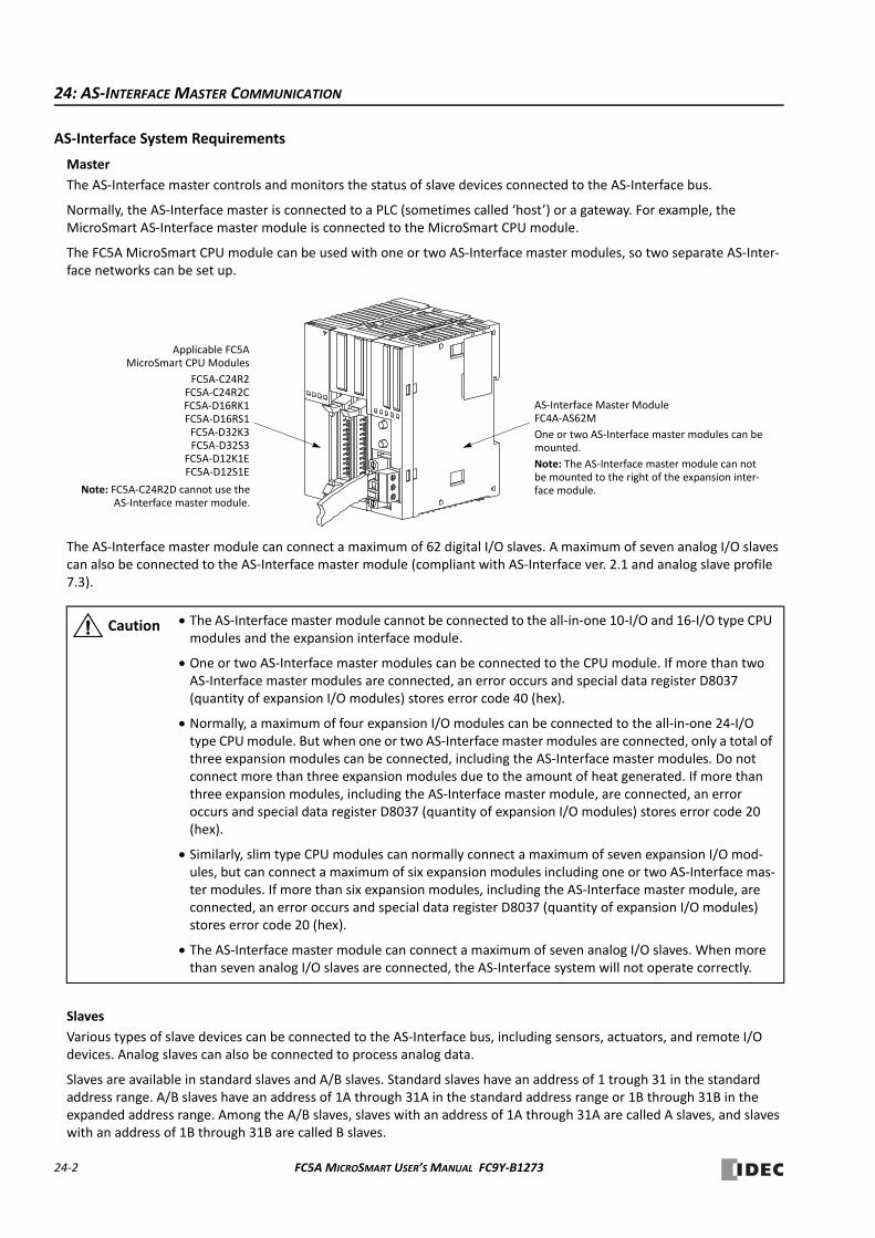
24: AS‐INTERFACE MASTER COMMUNICATION
AS‐Interface System Requirements
Master
The AS‐Interface master controls and monitors the status of slave devices connected to the AS‐Interface bus.
Normally, the AS‐Interface master is connected to a PLC (sometimes called ‘host’) or a gateway. For example, the MicroSmart AS‐Interface master module is connected to the MicroSmart CPU module.
The FC5A MicroSmart CPU module can be used with one or two AS‐Interface master modules, so two separate AS‐Inter‐face networks can be set up.
The AS‐Interface master module can connect a maximum of 62 digital I/O slaves. A maximum of seven analog I/O slaves can also be connected to the AS‐Interface master module (compliant with AS‐Interface ver. 2.1 and analog slave profile 7.3).
Slaves
Various types of slave devices can be connected to the AS‐Interface bus, including sensors, actuators, and remote I/O devices. Analog slaves can also be connected to process analog data.
Slaves are available in standard slaves and A/B slaves. Standard slaves have an address of 1 trough 31 in the standard address range. A/B slaves have an address of 1A through 31A in the standard address range or 1B through 31B in the expanded address range. Among the A/B slaves, slaves with an address of 1A through 31A are called A slaves, and slaves with an address of 1B through 31B are called B slaves.
The AS‐Interface master module cannot be connected to the all‐in‐one 10‐I/O and 16‐I/O type CPU modules and the expansion interface module.
One or two AS‐Interface master modules can be connected to the CPU module. If more than two AS‐Interface master modules are connected, an error occurs and special data register D8037 (quantity of expansion I/O modules) stores error code 40 (hex).
Normally, a maximum of four expansion I/O modules can be connected to the all‐in‐one 24‐I/O type CPU module. But when one or two AS‐Interface master modules are connected, only a total of three expansion modules can be connected, including the AS‐Interface master modules. Do not connect more than three expansion modules due to the amount of heat generated. If more than three expansion modules, including the AS‐Interface master module, are connected, an error occurs and special data register D8037 (quantity of expansion I/O modules) stores error code 20 (hex).
Similarly, slim type CPU modules can normally connect a maximum of seven expansion I/O mod‐ules, but can connect a maximum of six expansion modules including one or two AS‐Interface mas‐ter modules. If more than six expansion modules, including the AS‐Interface master module, are connected, an error occurs and special data register D8037 (quantity of expansion I/O modules) stores error code 20 (hex).
The AS‐Interface master module can connect a maximum of seven analog I/O slaves. When more than seven analog I/O slaves are connected, the AS‐Interface system will not operate correctly.
AS‐Interface Master ModuleFC4A‐AS62M
One or two AS‐Interface master modules can be mounted.
Note: The AS‐Interface master module can not be mounted to the right of the expansion inter‐face module.
Applicable FC5AMicroSmart CPU Modules
FC5A‐C24R2FC5A‐C24R2CFC5A‐D16RK1FC5A‐D16RS1FC5A‐D32K3FC5A‐D32S3
FC5A‐D12K1EFC5A‐D12S1E
Note: FC5A‐C24R2D cannot use theAS‐Interface master module.
Caution
24‐2 FC5A MICROSMART USER’S MANUAL FC9Y‐B1273

24: AS‐INTERFACE MASTER COMMUNICATION
AS‐Interface Power Supply
The AS‐Interface bus uses a dedicated 30V DC power supply (AS‐Interface power supply), which is indicated with the AS‐Interface mark. General‐purpose power sup‐ply units cannot be used for the AS‐Interface bus.
When using two AS‐Interface master modules, two AS‐Interface power supplies are needed. Since the AS‐Interface cable transmits both signals and power, each net‐work requires a separate power supply.
Recommended IDEC AS‐Interface Power Supplies
Cables
The AS‐Interface bus uses only one cable to transmit signals and power. Use one of the following cable types (the wire does not have to be stranded).
Standard yellow unshielded AS‐Interface cable (with polarity)
Ordinary two‐wire flat cable
Applicable Cable Specifications
Note: When using single wires, the maximum cable length is 200 mm. See “Maximum Communication Distance” on page 24‐1.
Use a VLSV (very low safety voltage) to power the AS‐Interface bus. The normal output voltage of the AS‐Interface power supply is 30V DC.
Input Voltage Output Voltage Output Wattage Type No.
100 to 240V AC 30.5V DC73W PS2R‐Q30ABL
145W PS2R‐F30ABL
Cable Type Cable Size/Manufacturer Cross‐sectional View
AS‐Interface Standard Cable
Cable sheath color: YellowConductor cross section: 1.5 mm2
LAPP’s CablesType No: 2170228 (sheath material EPDM)Type No: 2170230 (sheath material TPE)
2‐wire Flat CableorSingle Wires(See Note)
Conductor cross sectionStranded wire: 0.5 to 1.0 mm2
Solid wire: 0.75 to 1.5 mm2
AWG: 20 to 16
AS‐Interface Marks
Caution
AS‐Interface Cable Two‐wire Flat Cable
AS‐Interface – AS‐Interface + (blue) (brown)
AS‐Interface – AS‐Interface + (blue) (brown)
FC5A MICROSMART USER’S MANUAL FC9Y‐B1273 24‐3
24: AS‐INTERFACE MASTER COMMUNICATION
Main Features of AS‐Interface V2 with Slave Expansion Capability
The AS‐Interface is a reliable bus management system in which one master periodically monitors each slave device con‐nected on the AS‐Interface bus in sequence. The master manages the I/O data, parameters, and identification codes of each slave in addition to slave addresses. The management data depends on the type of the slave as follows:
Standard Slaves
A maximum of four inputs and four outputs for each slave Four parameters for setting a slave’s operation mode (P3, P2, P1, P0) Four identification codes (ID code, I/O code, ID2 code, and ID1 code)
A/B Slaves
A maximum of four inputs and three outputs for each slave Three parameters for setting a slave’s operation mode (P2, P1, P0) Four identification codes (ID code, I/O code, ID2 code, and ID1 code)
Note 1: Parameters P3 through P0 are used to set an operation mode of the slave. For details, see the user’s manual for the slave.
Note 2: The slaves connected to the AS‐Interface bus are distinguished from each other by the ID code and I/O code contained in each slave. Some slaves have ID2 code and ID1 code to indicate the internal functions of the slave. For example, analog slaves use the ID2 code to represent the channel number of the slave.
Note 3: The MicroSmart AS‐Interface master module is also compatible with AS‐Interface ver. 2.1 and earlier slaves.
Slave Addresses
Each standard slave connected to the AS‐Interface bus can be allocated an address of 1 through 31. Each A/B slave can be allocated an address of 1A through 31A or 1B through 31B. All slaves are set to address 0 at factory before shipment. The address of a slave can be changed using the “addressing tool.” Using WindLDR, the addresses of slaves connected to the AS‐Interface master modules 1 and 2 can also be changed (see page 24‐35).
When a slave fails during operation and needs to be replaced, if the auto addressing function is enabled on the master module, just replace the slave with a new one (with address 0 and the same identification codes). The new slave will automatically be allocated the same address as the slave that was removed, and you do not have to set the address again. For details of the ASI command to enable auto addressing, see page 24‐30.
Slave Identification
Slaves have the following four identification codes. The master checks the identification codes to determine the type and feature of the slave connected on the AS‐Interface bus.
ID Code
The ID code consists of 4 bits to indicate the type of the slave, such as sensor, actuator, standard slave, or A/B slave. For example, the ID code for a standard remote I/O is 0, and that for an A/B slave is A (hex).
I/O Code
The I/O code consists of 4 bits to indicate the quantity and allocation of I/O points on a slave.
I: input, O: output, B: input and output
ID2 Code
The ID2 code consists of 4 bits to indicate the internal function of the slave.
ID1 Code
The ID1 code consists of 4 bits to indicate additional identification of the slave. Standard slaves can have an ID1 code of 0000 through 1111 (bin). A/B slaves use the MSB to indicate A or B slave, and can have a unique value only for the lower three bits. The MSB of A slaves is set to 0, and that of B slaves is set to 1.
I/O Code Allocation I/O Code Allocation I/O Code Allocation I/O Code Allocation
0h I, I, I, I 4h I, I, B, B 8h O, O, O, O Ch O, O, B, B
1h I, I, I, O 5h I, O, O, O 9h O, O, O, I Dh O, I, I, I
2h I, I, I, B 6h I, B, B, B Ah O, O, O, B Eh O, B, B, B
3h I, I, O, O 7h B, B, B, B Bh O, O, I, I Fh (reserved)
24‐4 FC5A MICROSMART USER’S MANUAL FC9Y‐B1273

24: AS‐INTERFACE MASTER COMMUNICATION
Quantities of Slaves and I/O Points
The quantity of slaves that can be connected to one AS‐Interface master module is as follows.
Standard slaves: 31 maximum
A/B slaves: 62 maximum
The limits for slave quantities given above apply when the slaves are either all standard slaves or are all A/B slaves.
When 62 A/B slaves (with four inputs and three outputs) are connected, a maximum of 434 I/O points (248 inputs and 186 outputs) can be controlled by one AS‐Interface master module.
When using a mix of standard slaves and A/B slaves together, the standard slaves can only use addresses 1(A) through 31(A). Also, when a standard slave takes a certain address, the B address of the same number cannot be used for A/B slaves.
AS‐Interface Bus Topology and Maximum Length
The AS‐Interface bus topology is flexible, and you can wire the bus freely according to your requirements.
When repeaters or extenders are not used, the bus length can be 100m (328 feet) at the maximum.
The FC4A‐AS62M AS‐Interface master module can use two repeaters to extend the bus length to 300m.
AS‐Interface Bus Cycle Time
The AS‐Interface bus cycle time is the amount of time required for a master to cycle through every slave on the bus.
The information for each slave is continuously transmitted over the bus in sequence, so the AS‐Interface bus cycle time depends on the quantity of active slaves.
When up to 19 slaves are active, the bus cycle time is 3 ms.
When 20 to 62 slaves are active, the bus cycle time is 0.156 (1+N) ms where N is the number of slaves.
When A slave and B slave have the same address number (e.g. 12A and 12B), the two slaves are alternately updated each cycle. Therefore, when the system consists of 31 A slaves and 31 B slaves, then the AS‐Interface bus cycle time will be 10 ms.
Maximum AS‐Interface Bus Cycle Time
When 31 slaves are connected, the maximum bus cycle time is 5 ms.
When 62 slaves are connected, the maximum bus cycle time is 10 ms.
High Reliability and Security
The AS‐Interface employs a transfer process of high reliability and high security. The master monitors the AS‐Interface power supply voltage and data transmitted on the bus, and detects slave failures and data errors.
Even when a slave is replaced or a new slave is added during operation, the AS‐Interface master module need not be shut down and can continue uninterrupted communication with other active slaves on the bus.
FC5A MICROSMART USER’S MANUAL FC9Y‐B1273 24‐5

24: AS‐INTERFACE MASTER COMMUNICATION
Operation BasicsThis section describes simple operating procedures for the basic AS‐Interface system from programming WindLDR on a computer to monitoring the slave operation.
AS‐Interface System Setup
The sample AS‐Interface system consists of the following devices:
AS‐Interface Cable Wiring
Before wiring the AS‐Interface cable, remove the AS‐Interface cable terminal block from the AS‐Interface cable connector on the AS‐Interface master module.
AS‐Interface specifies use of brown cables for the AS‐Interface + line, and blue cables for the AS‐Interface – line. Connect the cables to match the color labels on the terminal block. Tighten the terminal screws to a torque of 0.5 to 0.6 N∙m.
Insert the terminal block to the connector on the AS‐Interface master module, and tighten the mounting screws to a torque of 0.3 to 0.5 N∙m.
Name Type No. Description
FC5A MicroSmart Slim Type CPU Module FC5A‐D16RK1 —
MicroSmart AS‐Interface Master Module FC4A‐AS62M —
WindLDR FC9Y‐LP2CDW Version 5.0 or higher
AS‐Interface Standard Slave —1 unitAddress 0ID: 0, I/O: 7, ID2: F, ID1: 7
AS‐Interface Power Supply PS2R‐Q30ABL Output 30.5V DC, 2.4A (73W)
Slim Type CPU ModuleFC5A‐D16RK1
AS‐Interface Master ModuleFC4A‐AS62M
Standard AS‐Interface Cable
Computer Link Cable 4CFC2A‐KC4C3m (9.84 ft.) long
AS‐Interface Power Supply
Standard SlaveAddress 0ID: 0, I/O: 7, ID2: F, ID1: 7
Blue AS‐Interface –
Use a ferrule.
Brown AS‐Interface +
Use a ferrule. Blue Label
Brown Label
24‐6 FC5A MICROSMART USER’S MANUAL FC9Y‐B1273
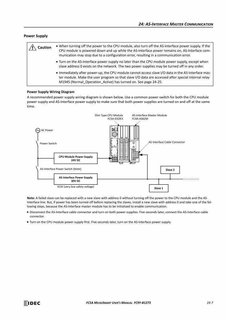
24: AS‐INTERFACE MASTER COMMUNICATION
Power Supply
Power Supply Wiring Diagram
A recommended power supply wiring diagram is shown below. Use a common power switch for both the CPU module power supply and AS‐Interface power supply to make sure that both power supplies are turned on and off at the same time.
Note: A failed slave can be replaced with a new slave with address 0 without turning off the power to the CPU module and the AS‐Interface line. But, if power has been turned off before replacing the slaves, install a new slave with address 0 and take one of the fol‐lowing steps, because the AS‐Interface master module has to be initialized to enable communication.
Disconnect the AS‐Interface cable connector and turn on both power supplies. Five seconds later, connect the AS‐Interface cable connector.
Turn on the CPU module power supply first. Five seconds later, turn on the AS‐Interface power supply.
When turning off the power to the CPU module, also turn off the AS‐Interface power supply. If the CPU module is powered down and up while the AS‐Interface power remains on, AS‐Interface com‐munication may stop due to a configuration error, resulting in a communication error.
Turn on the AS‐Interface power supply no later than the CPU module power supply, except when slave address 0 exists on the network. The two power supplies may be turned off in any order.
Immediately after power‐up, the CPU module cannot access slave I/O data in the AS‐Interface mas‐ter module. Make the user program so that slave I/O data are accessed after special internal relay M1945 (Normal_Operation_Active) has turned on. See page 24‐25.
Caution
AS‐Interface Power Supply30V DC
Slim Type CPU ModuleFC5A‐D32K3
AS‐Interface Master ModuleFC4A‐AS62M
Slave 1
Slave 2
AC Power
CPU Module Power Supply24V DC
Power Switch
AS‐Interface Power Switch (Note)
AS‐Interface Cable Connector
VLSV (very low safety voltage)
FC5A MICROSMART USER’S MANUAL FC9Y‐B1273 24‐7
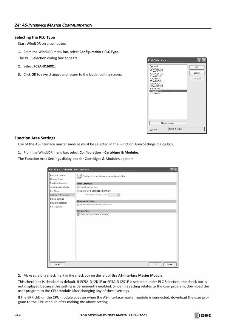
24: AS‐INTERFACE MASTER COMMUNICATION
Selecting the PLC Type
Start WindLDR on a computer.
1. From the WindLDR menu bar, select Configuration > PLC Type.
The PLC Selection dialog box appears.
2. Select FC5A‐D16RX1.
3. Click OK to save changes and return to the ladder editing screen.
Function Area Settings
Use of the AS‐Interface master module must be selected in the Function Area Settings dialog box.
1. From the WindLDR menu bar, select Configuration > Cartridges & Modules.
The Function Area Settings dialog box for Cartridges & Modules appears.
2. Make sure of a check mark in the check box on the left of Use AS‐Interface Master Module.
This check box is checked as default. If FC5A‐D12K1E or FC5A‐D12S1E is selected under PLC Selection, the check box is not displayed because this setting is permanently enabled. Since this setting relates to the user program, download the user program to the CPU module after changing any of these settings.
If the ERR LED on the CPU module goes on when the AS‐Interface master module is connected, download the user pro‐gram to the CPU module after making the above setting.
24‐8 FC5A MICROSMART USER’S MANUAL FC9Y‐B1273

24: AS‐INTERFACE MASTER COMMUNICATION
Assigning a Slave Address
AS‐Interface compatible slave devices are set to address 0 at factory. Connect the slave to the AS‐Interface master mod‐ule as shown on page 24‐6. Do not connect two or more slaves with slave address 0, otherwise the AS‐Interface master module cannot recognize slave addresses correctly.
1. Power up the MicroSmart CPU module first. Approximately 5 seconds later, turn on the AS‐Interface power supply.
Note: When slave address 0 is not mounted on the AS‐Interface bus, the CPU module power supply and the AS‐Interface power supply can be turned on at the same time. See page 24‐7.
2. From the WindLDR menu bar, select Online > Configure Master to open the Configure AS‐Interface Master dialog box. Press Refresh to collect slave information and update the screen display. (When configuration in the master module is complete, you do not have to press Refresh since the screen display is updated automatically.)
On the Configure AS‐Interface Master dialog box, slave address 0 is shaded with yellow. This means that the master mod‐ule has found slave address 0 on the AS‐Interface bus. The CDI for address 0 shows 07F7 (ID: 0, I/O: 7, ID2: F, ID1: 7).
3. Click the slave address “00” to open the Change Slave Address dialog box for slave 0. To assign slave address 1 to the slave, enter 1 in the New Address field and click OK.
The new address “01” is shaded with yellow to indicate that the address assignment is complete.
4. When changing slave addresses on other slaves, continue from step 3 if it is possible to wire the slave with‐out turning off power, or from step 1 if the CPU module is shut down.
Yellow Shade
Click slave address 0 to open theChange Slave Address dialog box.
CDI: Configuration Data ImagePCD: Permanent Configuration Data
Yellow Shade
FC5A MICROSMART USER’S MANUAL FC9Y‐B1273 24‐9
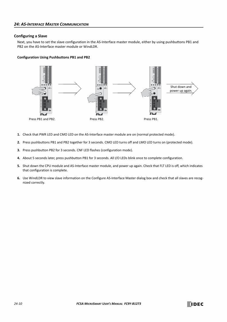
24: AS‐INTERFACE MASTER COMMUNICATION
Configuring a Slave
Next, you have to set the slave configuration in the AS‐Interface master module, either by using pushbuttons PB1 and PB2 on the AS‐Interface master module or WindLDR.
Configuration Using Pushbuttons PB1 and PB2
1. Check that PWR LED and CMO LED on the AS‐Interface master module are on (normal protected mode).
2. Press pushbuttons PB1 and PB2 together for 3 seconds. CMO LED turns off and LMO LED turns on (protected mode).
3. Press pushbutton PB2 for 3 seconds. CNF LED flashes (configuration mode).
4. About 5 seconds later, press pushbutton PB1 for 3 seconds. All I/O LEDs blink once to complete configuration.
5. Shut down the CPU module and AS‐Interface master module, and power up again. Check that FLT LED is off, which indicates that configuration is complete.
6. Use WindLDR to view slave information on the Configure AS‐Interface Master dialog box and check that all slaves are recog‐nized correctly.
Press PB1 and PB2. Press PB2. Press PB1.
Shut down andpower up again.
24‐10 FC5A MICROSMART USER’S MANUAL FC9Y‐B1273
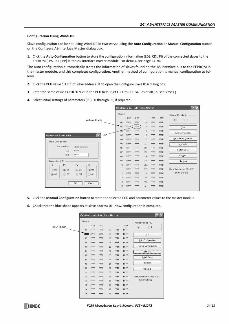
24: AS‐INTERFACE MASTER COMMUNICATION
Configuration Using WindLDR
Slave configuration can be set using WindLDR in two ways; using the Auto Configuration or Manual Configuration button on the Configure AS‐Interface Master dialog box.
1. Click the Auto Configuration button to store the configuration information (LDS, CDI, PI) of the connected slaves to the EEPROM (LPS, PCD, PP) in the AS‐Interface master module. For details, see page 24‐36.
The auto configuration automatically stores the information of slaves found on the AS‐Interface bus to the EEPROM in the master module, and this completes configuration. Another method of configuration is manual configuration as fol‐lows.
2. Click the PCD value “FFFF” of slave address 01 to open the Configure Slave 01A dialog box.
3. Enter the same value as CDI “07F7” in the PCD field. (Set FFFF to PCD values of all unused slaves.)
4. Select initial settings of parameters (PP) P0 through P3, if required.
5. Click the Manual Configuration button to store the selected PCD and parameter values to the master module.
6. Check that the blue shade appears at slave address 01. Now, configuration is complete.
Yellow Shade
Blue Shade
FC5A MICROSMART USER’S MANUAL FC9Y‐B1273 24‐11
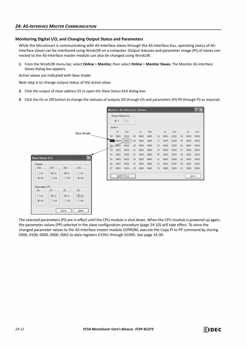
24: AS‐INTERFACE MASTER COMMUNICATION
Monitoring Digital I/O, and Changing Output Status and Parameters
While the MicroSmart is communicating with AS‐Interface slaves through the AS‐Interface bus, operating status of AS‐Interface slaves can be monitored using WindLDR on a computer. Output statuses and parameter image (PI) of slaves con‐nected to the AS‐Interface master module can also be changed using WindLDR.
1. From the WindLDR menu bar, select Online > Monitor, then select Online > Monitor Slaves. The Monitor AS‐Interface Slaves dialog box appears.
Active slaves are indicated with blue shade.
Next step is to change output status of the active slave.
2. Click the output of slave address 01 to open the Slave Status 01A dialog box.
3. Click the On or Off button to change the statuses of outputs O0 through O3 and parameters (PI) P0 through P3 as required.
The selected parameters (PI) are in effect until the CPU module is shut down. When the CPU module is powered up again, the parameter values (PP) selected in the slave configuration procedure (page 24‐10) will take effect. To store the changed parameter values to the AS‐Interface master module EEPROM, execute the Copy PI to PP command by storing 0306, 0100, 0000, 0000, 0001 to data registers D1941 through D1945. See page 24‐30.
Blue Shade
24‐12 FC5A MICROSMART USER’S MANUAL FC9Y‐B1273

24: AS‐INTERFACE MASTER COMMUNICATION
Troubles at System Start‐up
The following table summarizes possible troubles at system start‐up, probable causes and actions to be taken.
Trouble Cause and Action
PWR LED is off.(power)
AS‐Interface power is not supplied to the AS‐Interface master module. Check that wiring is correct and AS‐Interface power is supplied.
Power is not supplied from the CPU module to the AS‐Interface master module. Check the connection between the CPU module and the AS‐Interface master module.
FLT LED is on.(fault)
Slave configuration on the bus is incorrect. Use the WindLDR slave monitor function to check that slaves are connected correctly. Perform configuration, if necessary. For the con‐figuration method, see page 24‐34.
If FLT LED remains on even though slaves are connected correctly and configuration is com‐pleted, either disconnect and reconnect the AS‐Interface connector, or turn off and on the AS‐Interface power supply.
LMO LED is on.(local mode)
The CPU module fails to communicate with the AS‐Interface master module. Check the fol‐lowing points.
Is the CPU module compatible with AS‐Interface? Check the Type No. of the CPU module.
Is a check mark put in the check box “Use AS‐Interface Master Module” in WindLDR Func‐tion Area Settings? The box is checked as default. If not, put a check mark and download the user program to the CPU module.
OFF LED is on.(offline)
While a slave of address 0 was connected, power was turned on. After changing the slave address, power up again. For the address changing method, see page 24‐35.
Slave operation is unstable.
Check if there are two or more slaves with the same address. Each slave must have a unique address. If two slaves have the same address and same identification codes (ID, I/O, ID2, ID1), the AS‐Interface master module may fail to detect an error. When changing the dupli‐cate slave address using WindLDR, remove one of the slaves from the bus.
FC5A MICROSMART USER’S MANUAL FC9Y‐B1273 24‐13
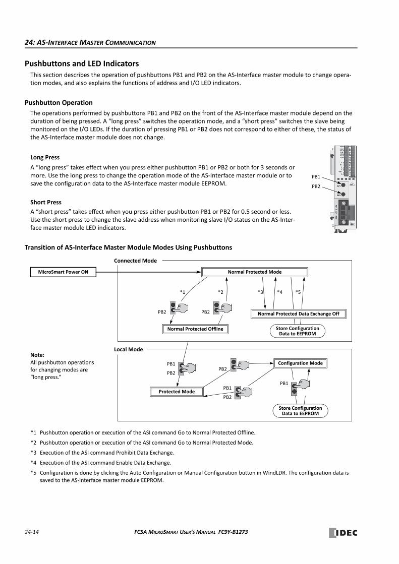
24: AS‐INTERFACE MASTER COMMUNICATION
Pushbuttons and LED IndicatorsThis section describes the operation of pushbuttons PB1 and PB2 on the AS‐Interface master module to change opera‐tion modes, and also explains the functions of address and I/O LED indicators.
Pushbutton Operation
The operations performed by pushbuttons PB1 and PB2 on the front of the AS‐Interface master module depend on the duration of being pressed. A “long press” switches the operation mode, and a “short press” switches the slave being monitored on the I/O LEDs. If the duration of pressing PB1 or PB2 does not correspond to either of these, the status of the AS‐Interface master module does not change.
Long Press
A “long press” takes effect when you press either pushbutton PB1 or PB2 or both for 3 seconds or more. Use the long press to change the operation mode of the AS‐Interface master module or to save the configuration data to the AS‐Interface master module EEPROM.
Short Press
A “short press” takes effect when you press either pushbutton PB1 or PB2 for 0.5 second or less. Use the short press to change the slave address when monitoring slave I/O status on the AS‐Inter‐face master module LED indicators.
Transition of AS‐Interface Master Module Modes Using Pushbuttons
*1 Pushbutton operation or execution of the ASI command Go to Normal Protected Offline.
*2 Pushbutton operation or execution of the ASI command Go to Normal Protected Mode.
*3 Execution of the ASI command Prohibit Data Exchange.
*4 Execution of the ASI command Enable Data Exchange.
*5 Configuration is done by clicking the Auto Configuration or Manual Configuration button in WindLDR. The configuration data is saved to the AS‐Interface master module EEPROM.
PB1
PB2
Normal Protected Offline Store ConfigurationData to EEPROM
Connected Mode
Normal Protected Data Exchange Off
*5*4*3
MicroSmart Power ON
*2*1
Local Mode
Configuration Mode
Protected Mode
Store ConfigurationData to EEPROM
PB1
Note: All pushbutton operations for changing modes are “long press.”
PB2
PB1
Normal Protected Mode
PB2 PB2
PB2
PB2
PB1
24‐14 FC5A MICROSMART USER’S MANUAL FC9Y‐B1273
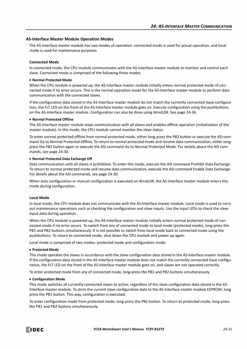
24: AS‐INTERFACE MASTER COMMUNICATION
AS‐Interface Master Module Operation Modes
The AS‐Interface master module has two modes of operation: connected mode is used for actual operation, and local mode is used for maintenance purposes.
Connected Mode
In connected mode, the CPU module communicates with the AS‐Interface master module to monitor and control each slave. Connected mode is comprised of the following three modes.
Normal Protected Mode
When the CPU module is powered up, the AS‐Interface master module initially enters normal protected mode of con‐nected mode if no error occurs. This is the normal operation mode for the AS‐Interface master module to perform data communication with the connected slaves.
If the configuration data stored in the AS‐Interface master module do not match the currently connected slave configura‐tion, the FLT LED on the front of the AS‐Interface master module goes on. Execute configuration using the pushbuttons on the AS‐Interface master module. Configuration can also be done using WindLDR. See page 24‐36.
Normal Protected Offline
The AS‐Interface master module stops communication with all slaves and enables offline operation (initialization of the master module). In this mode, the CPU module cannot monitor the slave status.
To enter normal protected offline from normal protected mode, either long‐press the PB2 button or execute the ASI com‐mand Go to Normal Protected Offline. To return to normal protected mode and resume data communication, either long‐press the PB2 button again or execute the ASI command Go to Normal Protected Mode. For details about the ASI com‐mands, see page 24‐30.
Normal Protected Data Exchange Off
Data communication with all slaves is prohibited. To enter this mode, execute the ASI command Prohibit Data Exchange. To return to normal protected mode and resume data communication, execute the ASI command Enable Data Exchange. For details about the ASI commands, see page 24‐30.
When auto configuration or manual configuration is executed on WindLDR, the AS‐Interface master module enters this mode during configuration.
Local Mode
In local mode, the CPU module does not communicate with the AS‐Interface master module. Local mode is used to carry out maintenance operations such as checking the configuration and slave inputs. Use the input LEDs to check the slave input data during operation.
When the CPU module is powered up, the AS‐Interface master module initially enters normal protected mode of con‐nected mode if no error occurs. To switch from any of connected mode to local mode (protected mode), long‐press the PB1 and PB2 buttons simultaneously. It is not possible to switch from local mode back to connected mode using the pushbuttons. To return to connected mode, shut down the CPU module and power up again.
Local mode is comprised of two modes: protected mode and configuration mode.
Protected Mode
This mode operates the slaves in accordance with the slave configuration data stored in the AS‐Interface master module. If the configuration data stored in the AS‐Interface master module does not match the currently connected slave configu‐ration, the FLT LED on the front of the AS‐Interface master module goes on, and slaves are not operated correctly.
To enter protected mode from any of connected mode, long‐press the PB1 and PB2 buttons simultaneously.
Configuration Mode
This mode switches all currently connected slaves to active, regardless of the slave configuration data stored in the AS‐Interface master module. To store the current slave configuration data to the AS‐Interface master module EEPROM, long press the PB1 button. This way, configuration is executed.
To enter configuration mode from protected mode, long‐press the PB2 button. To return to protected mode, long‐press the PB1 and PB2 buttons simultaneously.
FC5A MICROSMART USER’S MANUAL FC9Y‐B1273 24‐15
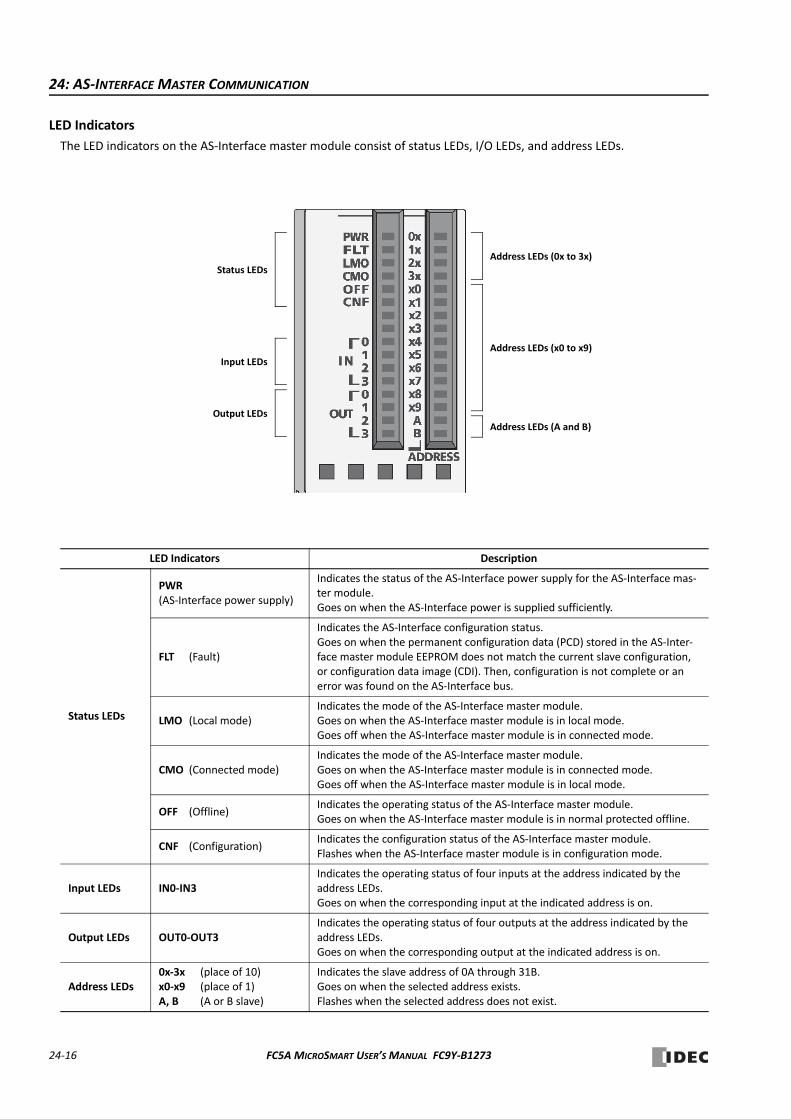
24: AS‐INTERFACE MASTER COMMUNICATION
LED Indicators
The LED indicators on the AS‐Interface master module consist of status LEDs, I/O LEDs, and address LEDs.
LED Indicators Description
Status LEDs
PWR(AS‐Interface power supply)
Indicates the status of the AS‐Interface power supply for the AS‐Interface mas‐ter module.Goes on when the AS‐Interface power is supplied sufficiently.
FLT (Fault)
Indicates the AS‐Interface configuration status. Goes on when the permanent configuration data (PCD) stored in the AS‐Inter‐face master module EEPROM does not match the current slave configuration, or configuration data image (CDI). Then, configuration is not complete or an error was found on the AS‐Interface bus.
LMO (Local mode)Indicates the mode of the AS‐Interface master module.Goes on when the AS‐Interface master module is in local mode.Goes off when the AS‐Interface master module is in connected mode.
CMO (Connected mode)Indicates the mode of the AS‐Interface master module.Goes on when the AS‐Interface master module is in connected mode.Goes off when the AS‐Interface master module is in local mode.
OFF (Offline)Indicates the operating status of the AS‐Interface master module.Goes on when the AS‐Interface master module is in normal protected offline.
CNF (Configuration)Indicates the configuration status of the AS‐Interface master module.Flashes when the AS‐Interface master module is in configuration mode.
Input LEDs IN0‐IN3Indicates the operating status of four inputs at the address indicated by the address LEDs.Goes on when the corresponding input at the indicated address is on.
Output LEDs OUT0‐OUT3Indicates the operating status of four outputs at the address indicated by the address LEDs.Goes on when the corresponding output at the indicated address is on.
Address LEDs0x‐3x (place of 10)x0‐x9 (place of 1)A, B (A or B slave)
Indicates the slave address of 0A through 31B.Goes on when the selected address exists.Flashes when the selected address does not exist.
Status LEDs
Input LEDs
Output LEDs
Address LEDs (x0 to x9)
Address LEDs (0x to 3x)
Address LEDs (A and B)
24‐16 FC5A MICROSMART USER’S MANUAL FC9Y‐B1273
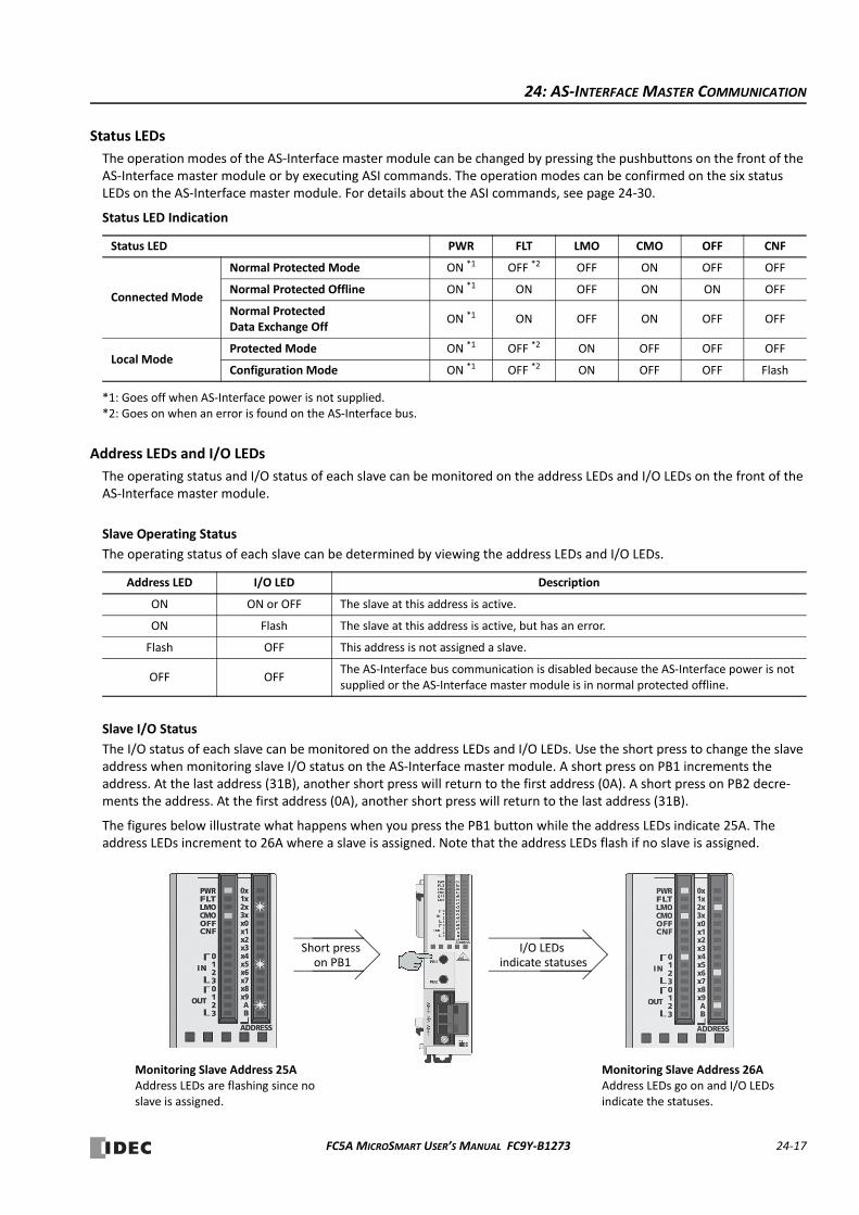
24: AS‐INTERFACE MASTER COMMUNICATION
Status LEDs
The operation modes of the AS‐Interface master module can be changed by pressing the pushbuttons on the front of the AS‐Interface master module or by executing ASI commands. The operation modes can be confirmed on the six status LEDs on the AS‐Interface master module. For details about the ASI commands, see page 24‐30.
Status LED Indication
*1: Goes off when AS‐Interface power is not supplied.*2: Goes on when an error is found on the AS‐Interface bus.
Address LEDs and I/O LEDs
The operating status and I/O status of each slave can be monitored on the address LEDs and I/O LEDs on the front of the AS‐Interface master module.
Slave Operating Status
The operating status of each slave can be determined by viewing the address LEDs and I/O LEDs.
Slave I/O Status
The I/O status of each slave can be monitored on the address LEDs and I/O LEDs. Use the short press to change the slave address when monitoring slave I/O status on the AS‐Interface master module. A short press on PB1 increments the address. At the last address (31B), another short press will return to the first address (0A). A short press on PB2 decre‐ments the address. At the first address (0A), another short press will return to the last address (31B).
The figures below illustrate what happens when you press the PB1 button while the address LEDs indicate 25A. The address LEDs increment to 26A where a slave is assigned. Note that the address LEDs flash if no slave is assigned.
Status LED PWR FLT LMO CMO OFF CNF
Connected Mode
Normal Protected Mode ON *1 OFF *2 OFF ON OFF OFF
Normal Protected Offline ON *1 ON OFF ON ON OFF
Normal Protected Data Exchange Off
ON *1 ON OFF ON OFF OFF
Local ModeProtected Mode ON *1 OFF *2 ON OFF OFF OFF
Configuration Mode ON *1 OFF *2 ON OFF OFF Flash
Address LED I/O LED Description
ON ON or OFF The slave at this address is active.
ON Flash The slave at this address is active, but has an error.
Flash OFF This address is not assigned a slave.
OFF OFFThe AS‐Interface bus communication is disabled because the AS‐Interface power is not supplied or the AS‐Interface master module is in normal protected offline.
Monitoring Slave Address 25AAddress LEDs are flashing since no slave is assigned.
Short press on PB1
I/O LEDs indicate statuses
Monitoring Slave Address 26AAddress LEDs go on and I/O LEDs indicate the statuses.
FC5A MICROSMART USER’S MANUAL FC9Y‐B1273 24‐17
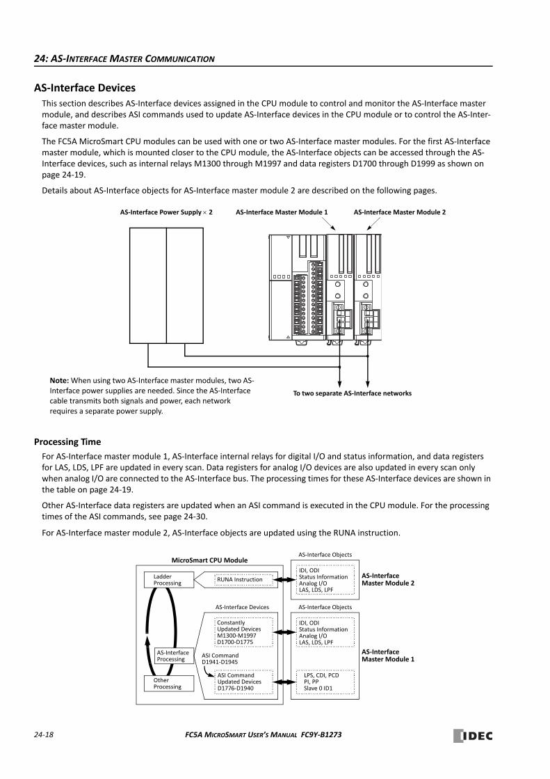
24: AS‐INTERFACE MASTER COMMUNICATION
AS‐Interface DevicesThis section describes AS‐Interface devices assigned in the CPU module to control and monitor the AS‐Interface master module, and describes ASI commands used to update AS‐Interface devices in the CPU module or to control the AS‐Inter‐face master module.
The FC5A MicroSmart CPU modules can be used with one or two AS‐Interface master modules. For the first AS‐Interface master module, which is mounted closer to the CPU module, the AS‐Interface objects can be accessed through the AS‐Interface devices, such as internal relays M1300 through M1997 and data registers D1700 through D1999 as shown on page 24‐19.
Details about AS‐Interface objects for AS‐Interface master module 2 are described on the following pages.
Processing Time
For AS‐Interface master module 1, AS‐Interface internal relays for digital I/O and status information, and data registers for LAS, LDS, LPF are updated in every scan. Data registers for analog I/O devices are also updated in every scan only when analog I/O are connected to the AS‐Interface bus. The processing times for these AS‐Interface devices are shown in the table on page 24‐19.
Other AS‐Interface data registers are updated when an ASI command is executed in the CPU module. For the processing times of the ASI commands, see page 24‐30.
For AS‐Interface master module 2, AS‐Interface objects are updated using the RUNA instruction.
AS‐Interface Master Module 1 AS‐Interface Master Module 2AS‐Interface Power Supply 2
To two separate AS‐Interface networks
Note: When using two AS‐Interface master modules, two AS‐Interface power supplies are needed. Since the AS‐Interface cable transmits both signals and power, each network requires a separate power supply.
LadderProcessing
OtherProcessing
AS‐InterfaceProcessing
Constantly Updated DevicesM1300‐M1997
ASI CommandD1941‐D1945
ASI Command
AS‐Interface
AS‐Interface Objects
IDI, ODI Status InformationAnalog I/OLAS, LDS, LPF
LPS, CDI, PCD PI, PP Slave 0 ID1D1776‐D1940
Updated Devices
D1700‐D1775
AS‐Interface Devices
Master Module 1
MicroSmart CPU Module
AS‐Interface Master Module 2
AS‐Interface Objects
IDI, ODI Status InformationAnalog I/OLAS, LDS, LPF
RUNA Instruction
24‐18 FC5A MICROSMART USER’S MANUAL FC9Y‐B1273
24: AS‐INTERFACE MASTER COMMUNICATION
Accessing AS‐Interface Objects for AS‐Interface Master Module 1
The I/O data and parameters of slaves on the AS‐Interface bus, the status of the AS‐Interface bus, and various list infor‐mation of the slaves are allocated to the AS‐Interface master module EEPROM. This information is called AS‐Interface objects, which can be accessed through the AS‐Interface devices, such as internal relays M1300 through M1997 and data registers D1700 through D1999. The allocation for AS‐Interface master module 1 is shown in the table below.
*1: The time required for the CPU module to update the device data. When using AS‐Interface master module 1, the scan time increases by a minimum of 10 ms. For AS‐Interface master module 2, see page 24‐32.
*2: These AS‐Interface device data can be read or written using WindLDR. For details, see page 24‐34.
*3: The LPS, PCD, and PP are set and downloaded to the CPU module using WindLDR. For details, see page 24‐36.
*4: The analog I/O data is updated only when an analog slave is connected to the AS‐Interface bus.
Accessing AS‐Interface Objects for AS‐Interface Master Module 2
When using two AS‐Interface master modules, the AS‐Interface objects for the second AS‐Interface master module can be assigned to any internal relays and data registers and accessed using RUNA or STPA instructions. See page 24‐32.
MicroSmart CPU Module Device Address Precessing
Time (ms) *1Read/Write
AS‐Interface Master Module EEPROMDevice Updated
DeviceAS‐Interface
Master Module 1AS‐Interface Object
AS‐Interface Internal Relays
M1300‐M1617 3.0 R *2 Digital input (IDI: input data image)
Every scan
M1620‐M1937 3.0 W *2 Digital output (ODI: output data image)
M1940‐M1997 1.0 R Status information
AS‐Interface Data Registers
D1700‐D1731 5.2 R Analog input *4
D1732‐D1763 5.2 W Analog output *4
D1764‐D1767 1.0 R *2 List of active slaves (LAS)
D1768‐D1771 1.0 R *2 List of detected slaves (LDS)
D1772‐D1775 1.0 R *2 List of peripheral fault slaves (LPF)
D1776‐D1779 1.0 R/W *2*3 List of projected slaves (LPS)
Each time ASI command is executed
D1780‐D1811 5.2 R *2 Configuration data image A (CDI)
D1812‐D1843 5.2 R *2 Configuration data image B (CDI)
D1844‐D1875 5.2 R/W *2*3 Permanent configuration data A (PCD)
D1876‐D1907 5.2 R/W *2*3 Permanent configuration data B (PCD)
D1908‐D1923 3.0 R *2 Parameter image (PI)
D1924‐D1939 3.0 R/W *2*3 Permanent parameter (PP)
D1940 0.7 R/W Slave 0 ID1 code
D1941‐D1945 — R/W ASI command description —
D1946‐D1999 — — (reserved) —
FC5A MICROSMART USER’S MANUAL FC9Y‐B1273 24‐19
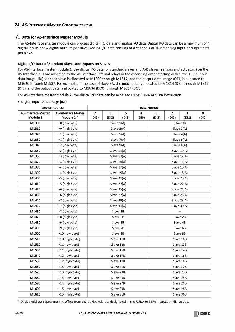
24: AS‐INTERFACE MASTER COMMUNICATION
I/O Data for AS‐Interface Master Module
The AS‐Interface master module can process digital I/O data and analog I/O data. Digital I/O data can be a maximum of 4 digital inputs and 4 digital outputs per slave. Analog I/O data consists of 4 channels of 16‐bit analog input or output data per slave.
Digital I/O Data of Standard Slaves and Expansion Slaves
For AS‐Interface master module 1, the digital I/O data for standard slaves and A/B slaves (sensors and actuators) on the AS‐Interface bus are allocated to the AS‐Interface internal relays in the ascending order starting with slave 0. The input data image (IDI) for each slave is allocated to M1300 through M1617, and the output data image (ODI) is allocated to M1620 through M1937. For example, in the case of slave 3A, the input data is allocated to M1314 (DI0) through M1317 (DI3), and the output data is allocated to M1634 (DO0) through M1637 (DO3).
For AS‐Interface master module 2, the digital I/O data can be accessed using RUNA or STPA instruction.
Digital Input Data Image (IDI)
* Device Address represents the offset from the Device Address designated in the RUNA or STPA instruction dialog box.
Device Address Data Format
AS‐Interface Master Module 1
AS‐Interface Master Module 2 *
7(DI3)
6(DI2)
5(DI1)
4(DI0)
3(DI3)
2(DI2)
1(DI1)
0(DI0)
M1300 +0 (low byte) Slave 1(A) (Slave 0)
M1310 +0 (high byte) Slave 3(A) Slave 2(A)
M1320 +1 (low byte) Slave 5(A) Slave 4(A)
M1330 +1 (high byte) Slave 7(A) Slave 6(A)
M1340 +2 (low byte) Slave 9(A) Slave 8(A)
M1350 +2 (high byte) Slave 11(A) Slave 10(A)
M1360 +3 (low byte) Slave 13(A) Slave 12(A)
M1370 +3 (high byte) Slave 15(A) Slave 14(A)
M1380 +4 (low byte) Slave 17(A) Slave 16(A)
M1390 +4 (high byte) Slave 19(A) Slave 18(A)
M1400 +5 (low byte) Slave 21(A) Slave 20(A)
M1410 +5 (high byte) Slave 23(A) Slave 22(A)
M1420 +6 (low byte) Slave 25(A) Slave 24(A)
M1430 +6 (high byte) Slave 27(A) Slave 26(A)
M1440 +7 (low byte) Slave 29(A) Slave 28(A)
M1450 +7 (high byte) Slave 31(A) Slave 30(A)
M1460 +8 (low byte) Slave 1B —
M1470 +8 (high byte) Slave 3B Slave 2B
M1480 +9 (low byte) Slave 5B Slave 4B
M1490 +9 (high byte) Slave 7B Slave 6B
M1500 +10 (low byte) Slave 9B Slave 8B
M1510 +10 (high byte) Slave 11B Slave 10B
M1520 +11 (low byte) Slave 13B Slave 12B
M1530 +11 (high byte) Slave 15B Slave 14B
M1540 +12 (low byte) Slave 17B Slave 16B
M1550 +12 (high byte) Slave 19B Slave 18B
M1560 +13 (low byte) Slave 21B Slave 20B
M1570 +13 (high byte) Slave 23B Slave 22B
M1580 +14 (low byte) Slave 25B Slave 24B
M1590 +14 (high byte) Slave 27B Slave 26B
M1600 +15 (low byte) Slave 29B Slave 28B
M1610 +15 (high byte) Slave 31B Slave 30B
24‐20 FC5A MICROSMART USER’S MANUAL FC9Y‐B1273
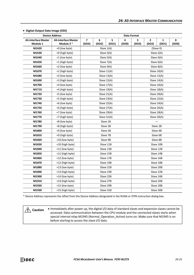
24: AS‐INTERFACE MASTER COMMUNICATION
Digital Output Data Image (ODI)
* Device Address represents the offset from the Device Address designated in the RUNA or STPA instruction dialog box.
Device Address Data Format
AS‐Interface Master Module 1
AS‐Interface Master Module 2 *
7(DO3)
6(DO2)
5(DO1)
4(DO0)
3(DO3)
2(DO2)
1(DO1)
0(DO0)
M1620 +0 (low byte) Slave 1(A) (Slave 0)
M1630 +0 (high byte) Slave 3(A) Slave 2(A)
M1640 +1 (low byte) Slave 5(A) Slave 4(A)
M1650 +1 (high byte) Slave 7(A) Slave 6(A)
M1660 +2 (low byte) Slave 9(A) Slave 8(A)
M1670 +2 (high byte) Slave 11(A) Slave 10(A)
M1680 +3 (low byte) Slave 13(A) Slave 12(A)
M1690 +3 (high byte) Slave 15(A) Slave 14(A)
M1700 +4 (low byte) Slave 17(A) Slave 16(A)
M1710 +4 (high byte) Slave 19(A) Slave 18(A)
M1720 +5 (low byte) Slave 21(A) Slave 20(A)
M1730 +5 (high byte) Slave 23(A) Slave 22(A)
M1740 +6 (low byte) Slave 25(A) Slave 24(A)
M1750 +6 (high byte) Slave 27(A) Slave 26(A)
M1760 +7 (low byte) Slave 29(A) Slave 28(A)
M1770 +7 (high byte) Slave 31(A) Slave 30(A)
M1780 +8 (low byte) Slave 1B —
M1790 +8 (high byte) Slave 3B Slave 2B
M1800 +9 (low byte) Slave 5B Slave 4B
M1810 +9 (high byte) Slave 7B Slave 6B
M1820 +10 (low byte) Slave 9B Slave 8B
M1830 +10 (high byte) Slave 11B Slave 10B
M1840 +11 (low byte) Slave 13B Slave 12B
M1850 +11 (high byte) Slave 15B Slave 14B
M1860 +12 (low byte) Slave 17B Slave 16B
M1870 +12 (high byte) Slave 19B Slave 18B
M1880 +13 (low byte) Slave 21B Slave 20B
M1890 +13 (high byte) Slave 23B Slave 22B
M1900 +14 (low byte) Slave 25B Slave 24B
M1910 +14 (high byte) Slave 27B Slave 26B
M1920 +15 (low byte) Slave 29B Slave 28B
M1930 +15 (high byte) Slave 31B Slave 30B
Immediately after power up, the digital I/O data of standard slaves and expansion slaves cannot be accessed. Data communication between the CPU module and the connected slaves starts when special internal relay M1945 (Normal_Operation_Active) turns on. Make sure that M1945 is on before starting to access the slave I/O data.
Caution
FC5A MICROSMART USER’S MANUAL FC9Y‐B1273 24‐21
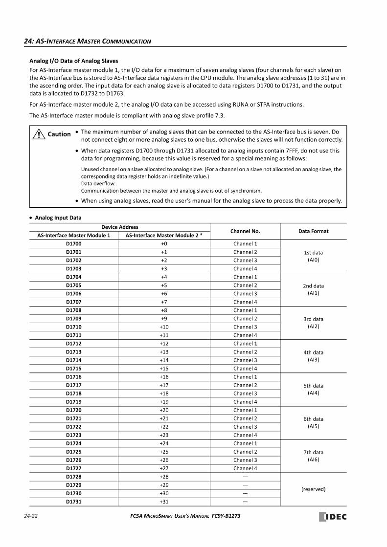
24: AS‐INTERFACE MASTER COMMUNICATION
Analog I/O Data of Analog Slaves
For AS‐Interface master module 1, the I/O data for a maximum of seven analog slaves (four channels for each slave) on the AS‐Interface bus is stored to AS‐Interface data registers in the CPU module. The analog slave addresses (1 to 31) are in the ascending order. The input data for each analog slave is allocated to data registers D1700 to D1731, and the output data is allocated to D1732 to D1763.
For AS‐Interface master module 2, the analog I/O data can be accessed using RUNA or STPA instructions.
The AS‐Interface master module is compliant with analog slave profile 7.3.
Analog Input Data
The maximum number of analog slaves that can be connected to the AS‐Interface bus is seven. Do not connect eight or more analog slaves to one bus, otherwise the slaves will not function correctly.
When data registers D1700 through D1731 allocated to analog inputs contain 7FFF, do not use this data for programming, because this value is reserved for a special meaning as follows:
Unused channel on a slave allocated to analog slave. (For a channel on a slave not allocated an analog slave, the corresponding data register holds an indefinite value.)Data overflow.Communication between the master and analog slave is out of synchronism.
When using analog slaves, read the user’s manual for the analog slave to process the data properly.
Device AddressChannel No. Data Format
AS‐Interface Master Module 1 AS‐Interface Master Module 2 *
D1700 +0 Channel 1
1st data(AI0)
D1701 +1 Channel 2
D1702 +2 Channel 3
D1703 +3 Channel 4
D1704 +4 Channel 1
2nd data(AI1)
D1705 +5 Channel 2
D1706 +6 Channel 3
D1707 +7 Channel 4
D1708 +8 Channel 1
3rd data(AI2)
D1709 +9 Channel 2
D1710 +10 Channel 3
D1711 +11 Channel 4
D1712 +12 Channel 1
4th data(AI3)
D1713 +13 Channel 2
D1714 +14 Channel 3
D1715 +15 Channel 4
D1716 +16 Channel 1
5th data(AI4)
D1717 +17 Channel 2
D1718 +18 Channel 3
D1719 +19 Channel 4
D1720 +20 Channel 1
6th data(AI5)
D1721 +21 Channel 2
D1722 +22 Channel 3
D1723 +23 Channel 4
D1724 +24 Channel 1
7th data(AI6)
D1725 +25 Channel 2
D1726 +26 Channel 3
D1727 +27 Channel 4
D1728 +28 —
(reserved)D1729 +29 —
D1730 +30 —
D1731 +31 —
Caution
24‐22 FC5A MICROSMART USER’S MANUAL FC9Y‐B1273
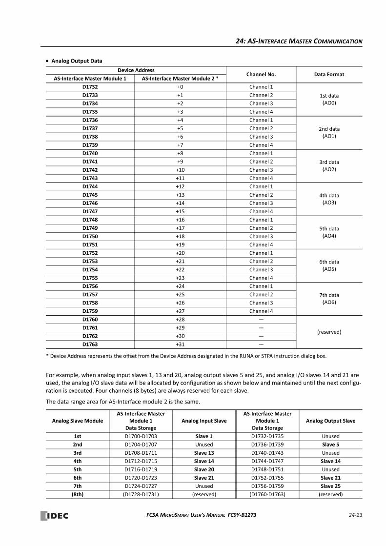
24: AS‐INTERFACE MASTER COMMUNICATION
Analog Output Data
* Device Address represents the offset from the Device Address designated in the RUNA or STPA instruction dialog box.
For example, when analog input slaves 1, 13 and 20, analog output slaves 5 and 25, and analog I/O slaves 14 and 21 are used, the analog I/O slave data will be allocated by configuration as shown below and maintained until the next configu‐ration is executed. Four channels (8 bytes) are always reserved for each slave.
The data range area for AS‐Interface module 2 is the same.
Device AddressChannel No. Data Format
AS‐Interface Master Module 1 AS‐Interface Master Module 2 *
D1732 +0 Channel 1
1st data(AO0)
D1733 +1 Channel 2
D1734 +2 Channel 3
D1735 +3 Channel 4
D1736 +4 Channel 1
2nd data(AO1)
D1737 +5 Channel 2
D1738 +6 Channel 3
D1739 +7 Channel 4
D1740 +8 Channel 1
3rd data(AO2)
D1741 +9 Channel 2
D1742 +10 Channel 3
D1743 +11 Channel 4
D1744 +12 Channel 1
4th data(AO3)
D1745 +13 Channel 2
D1746 +14 Channel 3
D1747 +15 Channel 4
D1748 +16 Channel 1
5th data(AO4)
D1749 +17 Channel 2
D1750 +18 Channel 3
D1751 +19 Channel 4
D1752 +20 Channel 1
6th data(AO5)
D1753 +21 Channel 2
D1754 +22 Channel 3
D1755 +23 Channel 4
D1756 +24 Channel 1
7th data(AO6)
D1757 +25 Channel 2
D1758 +26 Channel 3
D1759 +27 Channel 4
D1760 +28 —
(reserved)D1761 +29 —
D1762 +30 —
D1763 +31 —
Analog Slave ModuleAS‐Interface Master
Module 1 Data Storage
Analog Input SlaveAS‐Interface Master
Module 1 Data Storage
Analog Output Slave
1st D1700‐D1703 Slave 1 D1732‐D1735 Unused
2nd D1704‐D1707 Unused D1736‐D1739 Slave 5
3rd D1708‐D1711 Slave 13 D1740‐D1743 Unused
4th D1712‐D1715 Slave 14 D1744‐D1747 Slave 14
5th D1716‐D1719 Slave 20 D1748‐D1751 Unused
6th D1720‐D1723 Slave 21 D1752‐D1755 Slave 21
7th D1724‐D1727 Unused D1756‐D1759 Slave 25
(8th) (D1728‐D1731) (reserved) (D1760‐D1763) (reserved)
FC5A MICROSMART USER’S MANUAL FC9Y‐B1273 24‐23
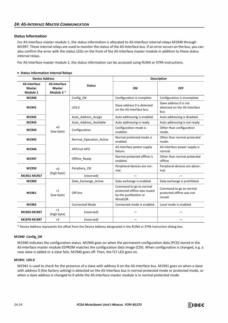
24: AS‐INTERFACE MASTER COMMUNICATION
Status Information
For AS‐Interface master module 1, the status information is allocated to AS‐Interface internal relays M1940 through M1997. These internal relays are used to monitor the status of the AS‐Interface bus. If an error occurs on the bus, you can also confirm the error with the status LEDs on the front of the AS‐Interface master module in addition to these status internal relays.
For AS‐Interface master module 2, the status information can be accessed using RUNA or STPA instructions.
Status Information Internal Relays
* Device Address represents the offset from the Device Address designated in the RUNA or STPA instruction dialog box.
M1940 Config_OK
M1940 indicates the configuration status. M1940 goes on when the permanent configuration data (PCD) stored in the AS‐Interface master module EEPROM matches the configuration data image (CDI). When configuration is changed, e.g. a new slave is added or a slave fails, M1940 goes off. Then, the FLT LED goes on.
M1941 LDS.0
M1941 is used to check for the presence of a slave with address 0 on the AS‐Interface bus. M1941 goes on when a slave with address 0 (the factory setting) is detected on the AS‐Interface bus in normal protected mode or protected mode, or when a slave address is changed to 0 while the AS‐Interface master module is in normal protected mode.
Device Address
Status
Description
AS‐Interface Master
Module 1
AS‐Interface Master
Module 2 *ON OFF
M1940
+0(low byte)
Config_OK Configuration is complete. Configuration is incomplete.
M1941 LDS.0Slave address 0 is detected on the AS‐Interface bus.
Slave address 0 is not detected on the AS‐Interface bus.
M1942 Auto_Address_Assign Auto addressing is enabled. Auto addressing is disabled.
M1943 Auto_Address_Available Auto addressing is ready. Auto addressing is not ready.
M1944 ConfigurationConfiguration mode is enabled.
Other than configuration mode.
M1945 Normal_Operation_ActiveNormal protected mode is enabled.
Other than normal protected mode.
M1946 APF/not APOAS‐Interface power supply failure.
AS‐Interface power supply is normal.
M1947 Offline_ReadyNormal protected offline is enabled.
Other than normal protected offline.
M1950 +0(high byte)
Periphery_OKPeripheral devices are nor‐mal.
Peripheral devices are abnor‐mal.
M1951‐M1957 (reserved) — —
M1960
+1(low byte)
Data_Exchange_Active Data exchange is enabled. Data exchange is prohibited.
M1961 Off‐line
Command to go to normal protected offline was issued by the pushbutton or WindLDR.
Command to go to normal protected offline was not issued.
M1962 Connected Mode Connected mode is enabled. Local mode is enabled.
M1963‐M1967+1
(high byte)(reserved) — —
M1970‐M1997 +2 (reserved) — —
24‐24 FC5A MICROSMART USER’S MANUAL FC9Y‐B1273
24: AS‐INTERFACE MASTER COMMUNICATION
M1942 Auto_Address_Assign
M1942 indicates that the auto addressing function is enabled. The default setting is “enabled,” and M1942 is normally on. This setting can be changed using the ASI commands Enable Auto Addressing and Disable Auto Addressing.
Note: When the auto addressing function is enabled at the AS‐Interface master module and a slave fails, you can replace the slave with a new slave which has the same identification codes without stopping the AS‐Interface bus.
If the replacement slave is assigned the same address and has the same identification codes as the failed slave, the replacement slave is automatically added to the LDS (list of detected slaves) to continue operation. If the assigned address or the identification codes of the replacement slave are different from the failed slave, the FLT LED will go on.
When replacing a failed slave with a new slave which is assigned address 0 (factory setting) and has the same identification codes, the new slave will be assigned the address of the failed slave and added to the LDS and LAS (list of active slaves). If the identification codes of the replacement slave are different from the failed slave, the FLT LED will go on.
The auto addressing function for a replacement slave works only when one slave has failed. This function cannot be used to replace multiple slaves.
M1943 Auto_Address_Available
M1943 indicates whether or not the conditions for the auto addressing function are satisfied. M1943 goes on when the auto addressing function is enabled and there is one faulty slave (a slave which cannot be recognized by the AS‐Interface master module) on the AS‐Interface bus.
M1944 Configuration
M1944 indicates whether the AS‐Interface master module is in configuration mode (on) or other mode (off). While con‐figuration mode is enabled, M1944 remains on, and the CNF LED flashes.
M1945 Normal_Operation_Active
M1945 remains on while the AS‐Interface master module is in normal protected mode. M1945 is off while in other modes. When M1945 turns on, the CPU module starts to exchange data communication with the connected slaves.
M1946 APF/not APO
M1946 goes on when the AS‐Interface power supply has failed, then the PWR LED goes off.
M1947 Offline_Ready
M1947 indicates that the AS‐Interface master module is in normal protected offline. While in normal protected offline, M1947 remains on and the OFF LED also remains on.
M1950 Periphery_OK
M1950 remains on while the AS‐Interface master module does not detect a failure in peripheral devices. When a failure is found, M1950 goes off.
M1960 Data_Exchange_Active
M1960 indicates that data exchange is enabled. While M1960 is on, the AS‐Interface master module is in normal pro‐tected mode, and data exchange between the AS‐Interface master module and slaves is enabled. The data exchange can be enabled and disabled using the ASI commands Enable Data Exchange and Prohibit Data Exchange.
M1961 Off‐line
M1961 goes on when a command to switch to normal protected offline is issued. To switch to normal protected offline from normal protected mode, either press the PB2 button on the AS‐Interface master module or issue the ASI command Go to Normal Protected Offline. M1961 remains on until normal protected offline is exited.
M1962 Connected Mode
M1962 indicates that the AS‐Interface master module is in connected mode. While in connected mode, M1962 remains on. Then, LMO LED remains off and the CMO LED remains on.
FC5A MICROSMART USER’S MANUAL FC9Y‐B1273 24‐25
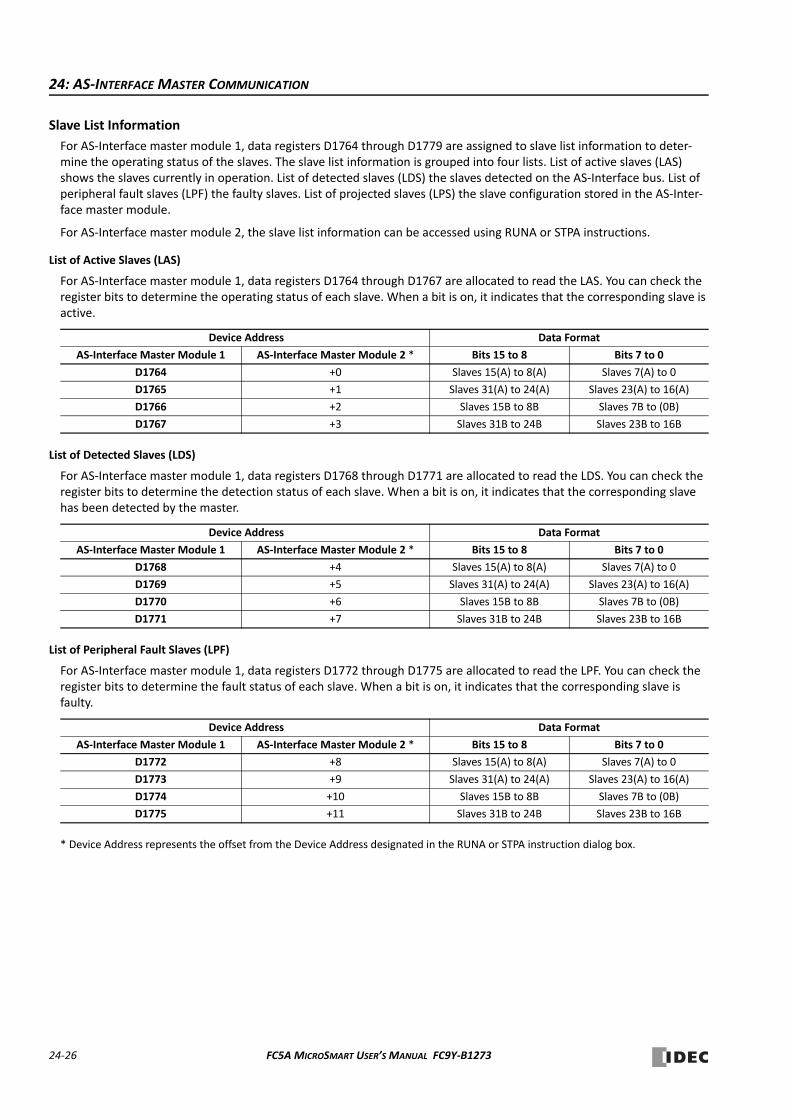
24: AS‐INTERFACE MASTER COMMUNICATION
Slave List Information
For AS‐Interface master module 1, data registers D1764 through D1779 are assigned to slave list information to deter‐mine the operating status of the slaves. The slave list information is grouped into four lists. List of active slaves (LAS) shows the slaves currently in operation. List of detected slaves (LDS) the slaves detected on the AS‐Interface bus. List of peripheral fault slaves (LPF) the faulty slaves. List of projected slaves (LPS) the slave configuration stored in the AS‐Inter‐face master module.
For AS‐Interface master module 2, the slave list information can be accessed using RUNA or STPA instructions.
List of Active Slaves (LAS)
For AS‐Interface master module 1, data registers D1764 through D1767 are allocated to read the LAS. You can check the register bits to determine the operating status of each slave. When a bit is on, it indicates that the corresponding slave is active.
List of Detected Slaves (LDS)
For AS‐Interface master module 1, data registers D1768 through D1771 are allocated to read the LDS. You can check the register bits to determine the detection status of each slave. When a bit is on, it indicates that the corresponding slave has been detected by the master.
List of Peripheral Fault Slaves (LPF)
For AS‐Interface master module 1, data registers D1772 through D1775 are allocated to read the LPF. You can check the register bits to determine the fault status of each slave. When a bit is on, it indicates that the corresponding slave is faulty.
* Device Address represents the offset from the Device Address designated in the RUNA or STPA instruction dialog box.
Device Address Data Format
AS‐Interface Master Module 1 AS‐Interface Master Module 2 * Bits 15 to 8 Bits 7 to 0
D1764 +0 Slaves 15(A) to 8(A) Slaves 7(A) to 0
D1765 +1 Slaves 31(A) to 24(A) Slaves 23(A) to 16(A)
D1766 +2 Slaves 15B to 8B Slaves 7B to (0B)
D1767 +3 Slaves 31B to 24B Slaves 23B to 16B
Device Address Data Format
AS‐Interface Master Module 1 AS‐Interface Master Module 2 * Bits 15 to 8 Bits 7 to 0
D1768 +4 Slaves 15(A) to 8(A) Slaves 7(A) to 0
D1769 +5 Slaves 31(A) to 24(A) Slaves 23(A) to 16(A)
D1770 +6 Slaves 15B to 8B Slaves 7B to (0B)
D1771 +7 Slaves 31B to 24B Slaves 23B to 16B
Device Address Data Format
AS‐Interface Master Module 1 AS‐Interface Master Module 2 * Bits 15 to 8 Bits 7 to 0
D1772 +8 Slaves 15(A) to 8(A) Slaves 7(A) to 0
D1773 +9 Slaves 31(A) to 24(A) Slaves 23(A) to 16(A)
D1774 +10 Slaves 15B to 8B Slaves 7B to (0B)
D1775 +11 Slaves 31B to 24B Slaves 23B to 16B
24‐26 FC5A MICROSMART USER’S MANUAL FC9Y‐B1273

24: AS‐INTERFACE MASTER COMMUNICATION
List of Projected Slaves (LPS)
For AS‐Interface master module 1, D1776 through D1779 are allocated to read and write the LPS. The LPS settings are stored to the AS‐Interface master module when either Auto Configuration or Manual Configuration is executed on WindLDR. The ASI command Read LPS can be used to read the LPS data to data registers D1776 through D1779. Then, you can check the register bits to determine the slave projection. When a bit is on, it indicates that the corresponding slave is set as a projected slave. After changing the LPS settings, execute the ASI command Read LPS, then you can use the updated data for program execution.
For AS‐Interface master module 2, the list of projected slaves cannot be accessed using the RUNA or STPA instruction.
Slave Identification Information (Slave Profile)
For AS‐Interface master module 1, data registers D1780 through D1940 are assigned to the slave identification informa‐tion, or the slave profile. The slave profile includes configuration data and parameters to indicate the slave type and slave operation, respectively.
For AS‐Interface master module 2, the slave identification information can not be accessed using RUNA or STPA instruc‐tions.
Configuration Data Image (CDI)
For AS‐Interface master module 1, data registers D1780 through D1843 are allocated to read the CDI of each slave. The CDI is the current slave configuration data collected by the AS‐Interface master module at power‐up and stored in the AS‐Interface master module.
The CDI is made up of four codes: the ID code, I/O code, ID2 code, and ID1 code. The CDI of slaves not connected to the AS‐Interface bus is FFFFh.
The ASI command Read CDI can be used to read the CDI data to data registers D1780 through D1843. Execute the ASI command Read CDI before using the CDI data for program execution.
Device Address Data Format
AS‐Interface Master Module 1 AS‐Interface Master Module 2 Bits 15 to 8 Bits 7 to 0
D1776 — Slaves 15(A) to 8(A) Slaves 7(A) to 0
D1777 — Slaves 31(A) to 24(A) Slaves 23(A) to 16(A)
D1778 — Slaves 15B to 8B Slaves 7B to (0B)
D1779 — Slaves 31B to 24B Slaves 23B to 16B
Device Address Data Format
AS‐Interface Master Module 1
AS‐Interface Master Module 2
Bits 15 to 12ID Code
Bits 11 to 8I/O Code
Bits 7 to 4ID2 Code
Bits 3 to 0ID1 Code
D1780 — Slave 0
D1781 — Slave 1(A)
D1782 — Slave 2(A)
D(1780+N) — Slave N(A)
D1811 — Slave 31(A)
D1812 — (unused)
D1813 — Slave 1B
D(1812+N) — Slave NB
D1843 — Slave 31B
FC5A MICROSMART USER’S MANUAL FC9Y‐B1273 24‐27

24: AS‐INTERFACE MASTER COMMUNICATION
Permanent Configuration Data (PCD)
For AS‐Interface master module 1, data registers D1844 through D1907 are allocated to read and write the PCD of each slave. Like the CDI, the PCD is made up of four codes: the ID code, I/O code, ID2 code, and ID1 code.
When auto configuration is executed, the CDI is copied to the PCD and stored in the ROM of the AS‐Interface master module. When you execute manual configuration, you can set the PCD using the Configure Slave dialog box on WindLDR. Set the PCD of each slave to the same value as its CDI. If the PCD is different from the CDI for a slave, then that slave does not function correctly. Set FFFFh to the PCD of vacant slave numbers.
The ASI command Read PCD can be used to read the PCD data to data registers D1844 through D1907. Execute the ASI command Read PCD before using the PCD data for program execution.
Parameter Image (PI)
For AS‐Interface master module 1, data registers D1908 through D1923 are allocated to read the PI of each slave. The PI is made up of four parameters: the P3, P2, P1, and P0. The PI is the current slave parameter data collected by the AS‐Inter‐face master module at power‐up and stored in the AS‐Interface master module. To change the PI settings, use WindLDR (Slave Status dialog box) or execute the ASI command Change Slave PI.
The ASI command Read PI can be used to read PI data to data registers D1908 through D1923. After changing the PI set‐tings, execute the ASI command Read PI, then you can use the updated PI data for program execution.
Device Address Data Format
AS‐Interface Master Module 1
AS‐Interface Master Module 2
Bits 15 to 12ID Code
Bits 11 to 8I/O Code
Bits 7 to 4ID2 Code
Bits 3 to 0ID1 Code
D1844 — Slave 0
D1845 — Slave 1(A)
D1846 — Slave 2(A)
D(1844+N) — Slave N(A)
D1875 — Slave 31(A)
D1876 — (unused)
D1877 — Slave 1B
D(1876+N) — Slave NB
D1907 — Slave 31B
Device Address Data Format
AS‐Interface Master Module 1
AS‐Interface Master Module 2
Bits 15 to 12P3/P2/P1/P0
Bits 11 to 8P3/P2/P1/P0
Bits 7 to 4P3/P2/P1/P0
Bits 3 to 0P3/P2/P1/P0
D1908 — Slave 3(A) Slave 2(A) Slave 1(A) Slave 0
D1909 — Slave 7(A) Slave 6(A) Slave 5(A) Slave 4(A)
D1910 — Slave 11(A) Slave 10(A) Slave 9(A) Slave 8(A)
D(1908+N/4) — Slave (N+3)(A) Slave (N+2)(A) Slave (N+1)(A) Slave N(A)
D1915 — Slave 31(A) Slave 30(A) Slave 29(A) Slave 28(A)
D1916 — Slave 3B Slave 2B Slave 1B (unused)
D1917 — Slave 7B Slave 6B Slave 5B Slave 4B
D(1916+N/4) — Slave (N+3)B Slave (N+2)B Slave (N+1)B Slave NB
D1923 — Slave 31B Slave 30B Slave 29B Slave 28B
24‐28 FC5A MICROSMART USER’S MANUAL FC9Y‐B1273
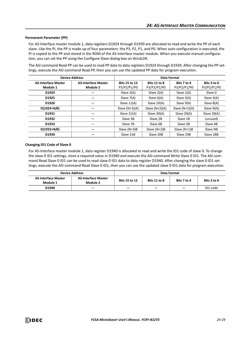
24: AS‐INTERFACE MASTER COMMUNICATION
Permanent Parameter (PP)
For AS‐Interface master module 1, data registers D1924 through D1939 are allocated to read and write the PP of each slave. Like the PI, the PP is made up of four parameters: the P3, P2, P1, and P0. When auto configuration is executed, the PI is copied to the PP and stored in the ROM of the AS‐Interface master module. When you execute manual configura‐tion, you can set the PP using the Configure Slave dialog box on WindLDR.
The ASI command Read PP can be used to read PP data to data registers D1924 through D1939. After changing the PP set‐tings, execute the ASI command Read PP, then you can use the updated PP data for program execution.
Changing ID1 Code of Slave 0
For AS‐Interface master module 1, data register D1940 is allocated to read and write the ID1 code of slave 0. To change the slave 0 ID1 settings, store a required value in D1940 and execute the ASI command Write Slave 0 ID1. The ASI com‐mand Read Slave 0 ID1 can be used to read slave 0 ID1 data to data register D1940. After changing the slave 0 ID1 set‐tings, execute the ASI command Read Slave 0 ID1, then you can use the updated slave 0 ID1 data for program execution.
Device Address Data Format
AS‐Interface Master Module 1
AS‐Interface Master Module 2
Bits 15 to 12P3/P2/P1/P0
Bits 11 to 8P3/P2/P1/P0
Bits 7 to 4P3/P2/P1/P0
Bits 3 to 0P3/P2/P1/P0
D1924 — Slave 3(A) Slave 2(A) Slave 1(A) Slave 0
D1925 — Slave 7(A) Slave 6(A) Slave 5(A) Slave 4(A)
D1926 — Slave 11(A) Slave 10(A) Slave 9(A) Slave 8(A)
D(1924+N/4) — Slave (N+3)(A) Slave (N+2)(A) Slave (N+1)(A) Slave N(A)
D1931 — Slave 31(A) Slave 30(A) Slave 29(A) Slave 28(A)
D1932 — Slave 3B Slave 2B Slave 1B (unused)
D1933 — Slave 7B Slave 6B Slave 5B Slave 4B
D(1932+N/4) — Slave (N+3)B Slave (N+2)B Slave (N+1)B Slave NB
D1939 — Slave 31B Slave 30B Slave 29B Slave 28B
Device Address Data Format
AS‐Interface Master Module 1
AS‐Interface Master Module 2
Bits 15 to 12 Bits 11 to 8 Bits 7 to 4 Bits 3 to 0
D1940 — — — — ID1 code
FC5A MICROSMART USER’S MANUAL FC9Y‐B1273 24‐29
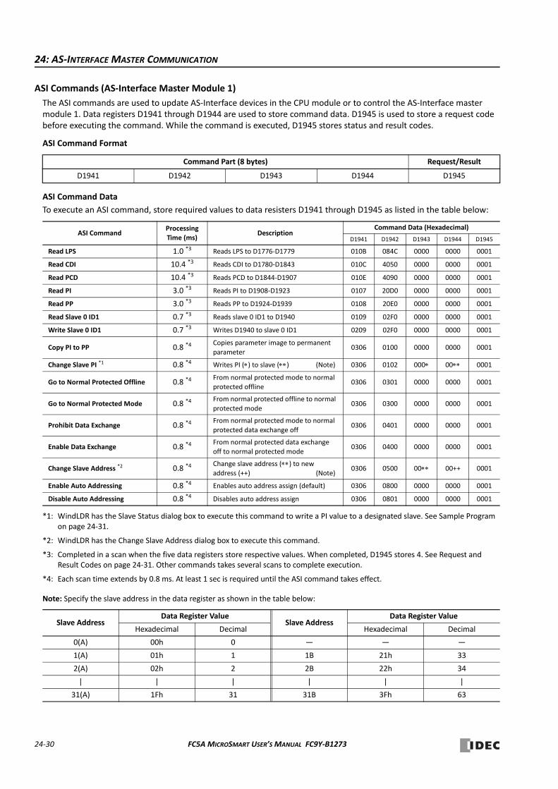
24: AS‐INTERFACE MASTER COMMUNICATION
ASI Commands (AS‐Interface Master Module 1)
The ASI commands are used to update AS‐Interface devices in the CPU module or to control the AS‐Interface master module 1. Data registers D1941 through D1944 are used to store command data. D1945 is used to store a request code before executing the command. While the command is executed, D1945 stores status and result codes.
ASI Command Format
ASI Command Data
To execute an ASI command, store required values to data resisters D1941 through D1945 as listed in the table below:
*1: WindLDR has the Slave Status dialog box to execute this command to write a PI value to a designated slave. See Sample Program on page 24‐31.
*2: WindLDR has the Change Slave Address dialog box to execute this command.
*3: Completed in a scan when the five data registers store respective values. When completed, D1945 stores 4. See Request and Result Codes on page 24‐31. Other commands takes several scans to complete execution.
*4: Each scan time extends by 0.8 ms. At least 1 sec is required until the ASI command takes effect.
Note: Specify the slave address in the data register as shown in the table below:
Command Part (8 bytes) Request/Result
D1941 D1942 D1943 D1944 D1945
ASI CommandProcessing Time (ms)
DescriptionCommand Data (Hexadecimal)
D1941 D1942 D1943 D1944 D1945
Read LPS 1.0 *3 Reads LPS to D1776‐D1779 010B 084C 0000 0000 0001
Read CDI 10.4 *3 Reads CDI to D1780‐D1843 010C 4050 0000 0000 0001
Read PCD 10.4 *3 Reads PCD to D1844‐D1907 010E 4090 0000 0000 0001
Read PI 3.0 *3 Reads PI to D1908‐D1923 0107 20D0 0000 0000 0001
Read PP 3.0 *3 Reads PP to D1924‐D1939 0108 20E0 0000 0000 0001
Read Slave 0 ID1 0.7 *3 Reads slave 0 ID1 to D1940 0109 02F0 0000 0000 0001
Write Slave 0 ID1 0.7 *3 Writes D1940 to slave 0 ID1 0209 02F0 0000 0000 0001
Copy PI to PP 0.8 *4Copies parameter image to permanent
parameter0306 0100 0000 0000 0001
Change Slave PI *1 0.8 *4 Writes PI () to slave () (Note) 0306 0102 000 00 0001
Go to Normal Protected Offline 0.8 *4From normal protected mode to normal protected offline
0306 0301 0000 0000 0001
Go to Normal Protected Mode 0.8 *4From normal protected offline to normal
protected mode0306 0300 0000 0000 0001
Prohibit Data Exchange 0.8 *4From normal protected mode to normal
protected data exchange off0306 0401 0000 0000 0001
Enable Data Exchange 0.8 *4From normal protected data exchange off to normal protected mode
0306 0400 0000 0000 0001
Change Slave Address *2 0.8 *4Change slave address () to new address (++) (Note)
0306 0500 00 00++ 0001
Enable Auto Addressing 0.8 *4 Enables auto address assign (default) 0306 0800 0000 0000 0001
Disable Auto Addressing 0.8 *4 Disables auto address assign 0306 0801 0000 0000 0001
Slave AddressData Register Value
Slave AddressData Register Value
Hexadecimal Decimal Hexadecimal Decimal
0(A) 00h 0 — — —
1(A) 01h 1 1B 21h 33
2(A) 02h 2 2B 22h 34
| | | | | |
31(A) 1Fh 31 31B 3Fh 63
24‐30 FC5A MICROSMART USER’S MANUAL FC9Y‐B1273
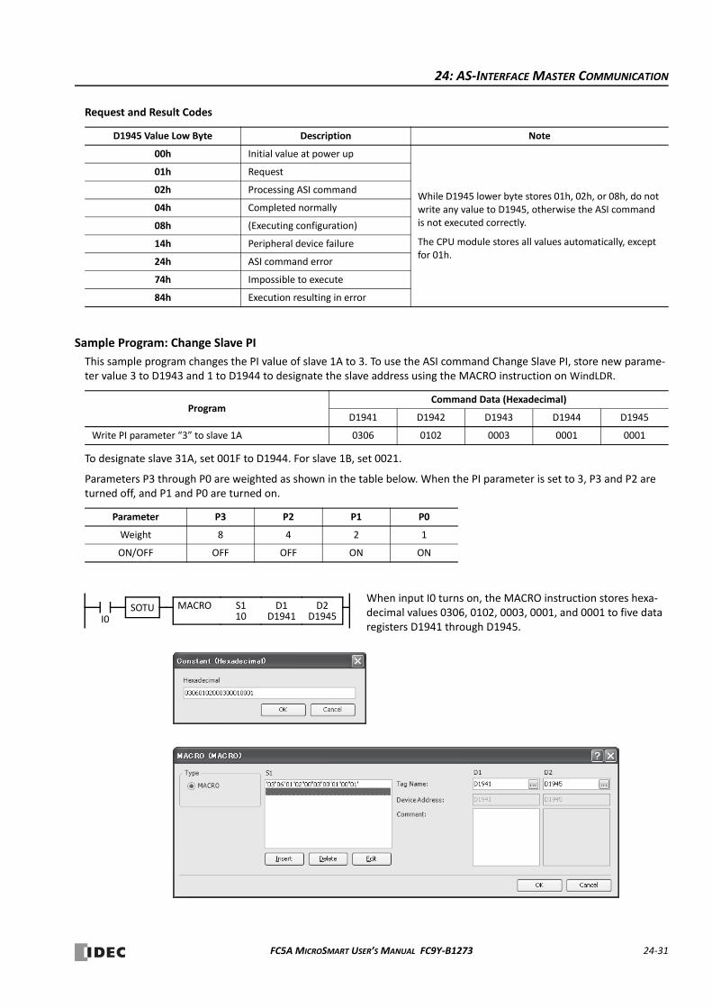
24: AS‐INTERFACE MASTER COMMUNICATION
Request and Result Codes
Sample Program: Change Slave PI
This sample program changes the PI value of slave 1A to 3. To use the ASI command Change Slave PI, store new parame‐ter value 3 to D1943 and 1 to D1944 to designate the slave address using the MACRO instruction on WindLDR.
To designate slave 31A, set 001F to D1944. For slave 1B, set 0021.
Parameters P3 through P0 are weighted as shown in the table below. When the PI parameter is set to 3, P3 and P2 are turned off, and P1 and P0 are turned on.
D1945 Value Low Byte Description Note
00h Initial value at power up
While D1945 lower byte stores 01h, 02h, or 08h, do not write any value to D1945, otherwise the ASI command is not executed correctly.
The CPU module stores all values automatically, except for 01h.
01h Request
02h Processing ASI command
04h Completed normally
08h (Executing configuration)
14h Peripheral device failure
24h ASI command error
74h Impossible to execute
84h Execution resulting in error
ProgramCommand Data (Hexadecimal)
D1941 D1942 D1943 D1944 D1945
Write PI parameter “3” to slave 1A 0306 0102 0003 0001 0001
Parameter P3 P2 P1 P0
Weight 8 4 2 1
ON/OFF OFF OFF ON ON
S110
D1D1941I0
SOTU MACRO D2D1945
When input I0 turns on, the MACRO instruction stores hexa‐decimal values 0306, 0102, 0003, 0001, and 0001 to five data registers D1941 through D1945.
FC5A MICROSMART USER’S MANUAL FC9Y‐B1273 24‐31

24: AS‐INTERFACE MASTER COMMUNICATION
Using Two AS‐Interface Master ModulesThe FC5A MicroSmart CPU modules can be used with one or two AS‐Interface master modules. For the first AS‐Interface master module, which is mounted closer to the CPU module, the AS‐Interface objects can be accessed through the AS‐Interface devices, such as internal relays M1300 through M1997 and data registers D1700 through D1999 as shown on page 24‐19.
Accessing AS‐Interface Objects for AS‐Interface Master Module 2
The I/O data and parameters of slaves on the AS‐Interface bus, the status of the AS‐Interface bus, and various list infor‐mation of the slaves are allocated to the AS‐Interface master module EEPROM. This information is called AS‐Interface objects. The AS‐Interface objects for the second AS‐Interface master module can be assigned to any internal relays and data registers and accessed using RUNA or STPA instructions.
The data addresses for AS‐Interface master module 2 are shown in the table below.
*1: The time required for the CPU module to update the device data for RUNA or STPA instruction. For example, when reading IDI, ODI, status information, LAS, LDS, and LPF continuously in every scan, the scan time increases by 10 ms.
*2: These AS‐Interface device data can be read or written using WindLDR. For details, see page 24‐34.
While performing master configuration or slave monitoring for AS‐Interface master module 2 using WindLDR, RUNA and STPA instructions for AS‐Interface master module 2 cannot be executed.
ASI commands cannot be used for AS‐Interface master module 2. Use pushbuttons PB1 and PB2 on the AS‐Interface master module to go to Normal Protected Mode, Normal Protected Offline, and Normal Protected Data Exchange Off.
AS‐Interface master module 2 does not have the function to change ID1 code of slave 1 and enable/disable auto addressing. Auto addressing is always enabled.
AS‐Interface Master Module 2Precessing Time (ms) *1
Read/Write
AS‐Interface Master Module EEPROM
Device AddressData Size (bytes)
AS‐Interface Object
0 32 3.0 R Digital input (IDI: input data image)
3 32 3.0 W Digital output (ODI: output data image)
2 6 1.0 R Status information
1 64 5.2 R Analog input
4 64 5.2 W Analog output
9 24 3.0 RList of active slaves (LAS)List of detected slaves (LDS)List of peripheral fault slaves (LPF)
— — — — List of projected slaves (LPS) *2
— — — — Configuration data image A (CDI) *2
— — — — Configuration data image B (CDI) *2
— — — — Permanent configuration data A (PCD) *2
— — — — Permanent configuration data B (PCD) *2
— — — — Parameter image (PI) *2
— — — — Permanent parameter (PP) *2
— — — — Slave 0 ID1 code
— — — — ASI command description
Caution
24‐32 FC5A MICROSMART USER’S MANUAL FC9Y‐B1273
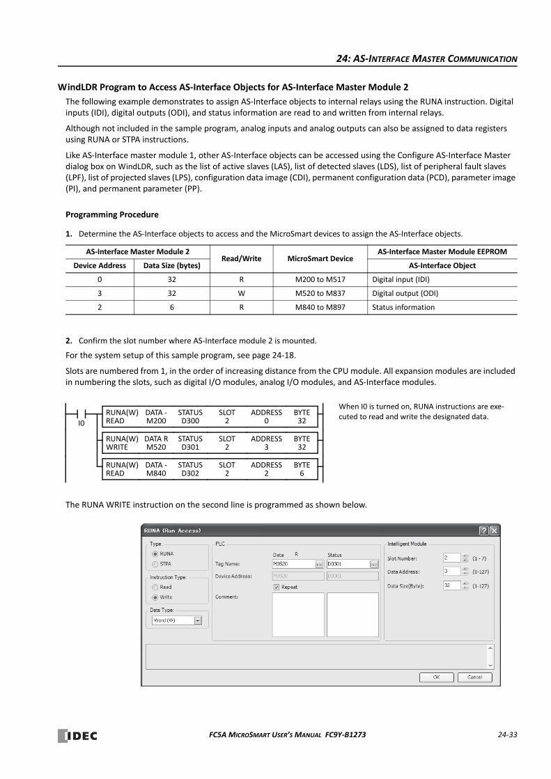
24: AS‐INTERFACE MASTER COMMUNICATION
WindLDR Program to Access AS‐Interface Objects for AS‐Interface Master Module 2
The following example demonstrates to assign AS‐Interface objects to internal relays using the RUNA instruction. Digital inputs (IDI), digital outputs (ODI), and status information are read to and written from internal relays.
Although not included in the sample program, analog inputs and analog outputs can also be assigned to data registers using RUNA or STPA instructions.
Like AS‐Interface master module 1, other AS‐Interface objects can be accessed using the Configure AS‐Interface Master dialog box on WindLDR, such as the list of active slaves (LAS), list of detected slaves (LDS), list of peripheral fault slaves (LPF), list of projected slaves (LPS), configuration data image (CDI), permanent configuration data (PCD), parameter image (PI), and permanent parameter (PP).
Programming Procedure
1. Determine the AS‐Interface objects to access and the MicroSmart devices to assign the AS‐Interface objects.
2. Confirm the slot number where AS‐Interface module 2 is mounted.
For the system setup of this sample program, see page 24‐18.
Slots are numbered from 1, in the order of increasing distance from the CPU module. All expansion modules are included in numbering the slots, such as digital I/O modules, analog I/O modules, and AS‐Interface modules.
The RUNA WRITE instruction on the second line is programmed as shown below.
AS‐Interface Master Module 2Read/Write MicroSmart Device
AS‐Interface Master Module EEPROM
Device Address Data Size (bytes) AS‐Interface Object
0 32 R M200 to M517 Digital input (IDI)
3 32 W M520 to M837 Digital output (ODI)
2 6 R M840 to M897 Status information
When I0 is turned on, RUNA instructions are exe‐cuted to read and write the designated data.
I0
DATA ‐M200
SLOT2
STATUSD300
BYTE32
ADDRESS0READ
RUNA(W)
DATA RM520
SLOT2
STATUSD301
BYTE32
ADDRESS3WRITE
RUNA(W)
DATA ‐M840
SLOT2
STATUSD302
BYTE6
ADDRESS2READ
RUNA(W)
FC5A MICROSMART USER’S MANUAL FC9Y‐B1273 24‐33
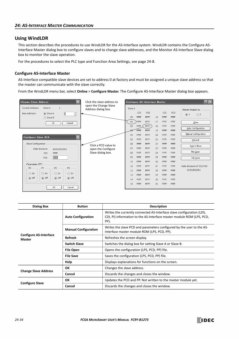
24: AS‐INTERFACE MASTER COMMUNICATION
Using WindLDRThis section describes the procedures to use WindLDR for the AS‐Interface system. WindLDR contains the Configure AS‐Interface Master dialog box to configure slaves and to change slave addresses, and the Monitor AS‐Interface Slave dialog box to monitor the slave operation.
For the procedures to select the PLC type and Function Area Settings, see page 24‐8.
Configure AS‐Interface Master
AS‐Interface compatible slave devices are set to address 0 at factory and must be assigned a unique slave address so that the master can communicate with the slave correctly.
From the WindLDR menu bar, select Online > Configure Master. The Configure AS‐Interface Master dialog box appears.
Dialog Box Button Description
Configure AS‐Interface Master
Auto ConfigurationWrites the currently connected AS‐Interface slave configuration (LDS, CDI, PI) information to the AS‐Interface master module ROM (LPS, PCD, PP).
Manual ConfigurationWrites the slave PCD and parameters configured by the user to the AS‐Interface master module ROM (LPS, PCD, PP).
Refresh Refreshes the screen display.
Switch Slave Switches the dialog box for setting Slave A or Slave B.
File Open Opens the configuration (LPS, PCD, PP) file.
File Save Saves the configuration (LPS, PCD, PP) file.
Help Displays explanations for functions on the screen.
Change Slave AddressOK Changes the slave address.
Cancel Discards the changes and closes the window.
Configure SlaveOK Updates the PCD and PP. Not written to the master module yet.
Cancel Discards the changes and closes the window.
Click the slave address to open the Change Slave Address dialog box.
Click a PCD value to open the Configure Slave dialog box.
24‐34 FC5A MICROSMART USER’S MANUAL FC9Y‐B1273
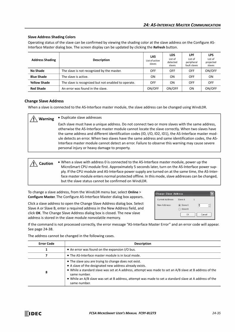
24: AS‐INTERFACE MASTER COMMUNICATION
Slave Address Shading Colors
Operating status of the slave can be confirmed by viewing the shading color at the slave address on the Configure AS‐Interface Master dialog box. The screen display can be updated by clicking the Refresh button.
Change Slave Address
When a slave is connected to the AS‐Interface master module, the slave address can be changed using WindLDR.
To change a slave address, from the WindLDR menu bar, select Online > Configure Master. The Configure AS‐Interface Master dialog box appears.
Click a slave address to open the Change Slave Address dialog box. Select Slave A or Slave B, enter a required address in the New Address field, and click OK. The Change Slave Address dialog box is closed. The new slave address is stored in the slave module nonvolatile memory.
If the command is not processed correctly, the error message “AS‐Interface Master Error” and an error code will appear. See page 24‐38.
The address cannot be changed in the following cases.
Address Shading DescriptionLAS
List of active slaves
LDSList of
detected slaves
LPFList of
peripheral fault slaves
LPSList of
projected slaves
No Shade The slave is not recognized by the master. OFF OFF OFF ON/OFF
Blue Shade The slave is active. ON ON OFF ON
Yellow Shade The slave is recognized but not enabled to operate. OFF ON OFF OFF
Red Shade An error was found in the slave. ON/OFF ON/OFF ON ON/OFF
Duplicate slave addresses
Each slave must have a unique address. Do not connect two or more slaves with the same address, otherwise the AS‐Interface master module cannot locate the slave correctly. When two slaves have the same address and different identification codes (ID, I/O, ID2, ID1), the AS‐Interface master mod‐ule detects an error. When two slaves have the same address and same identification codes, the AS‐Interface master module cannot detect an error. Failure to observe this warning may cause severe personal injury or heavy damage to property.
When a slave with address 0 is connected to the AS‐Interface master module, power up the MicroSmart CPU module first. Approximately 5 seconds later, turn on the AS‐Interface power sup‐ply. If the CPU module and AS‐Interface power supply are turned on at the same time, the AS‐Inter‐face master module enters normal protected offline. In this mode, slave addresses can be changed, but the slave status cannot be confirmed on WindLDR.
Error Code Description
1 An error was found on the expansion I/O bus.
7 The AS‐Interface master module is in local mode.
8
The slave you are trying to change does not exist. A slave of the designated new address already exists. While a standard slave was set at A address, attempt was made to set an A/B slave at B address of the same number.
While an A/B slave was set at B address, attempt was made to set a standard slave at A address of the same number.
Warning
Caution
FC5A MICROSMART USER’S MANUAL FC9Y‐B1273 24‐35
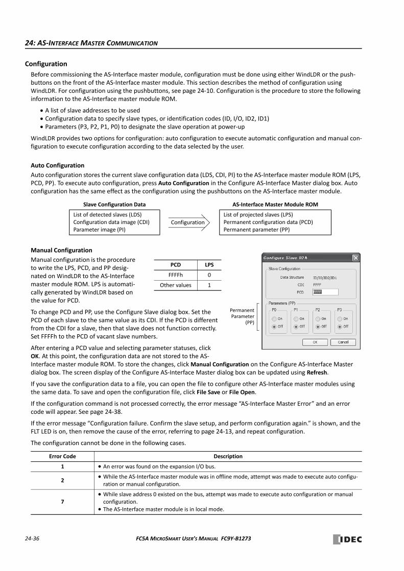
24: AS‐INTERFACE MASTER COMMUNICATION
Configuration
Before commissioning the AS‐Interface master module, configuration must be done using either WindLDR or the push‐buttons on the front of the AS‐Interface master module. This section describes the method of configuration using WindLDR. For configuration using the pushbuttons, see page 24‐10. Configuration is the procedure to store the following information to the AS‐Interface master module ROM.
A list of slave addresses to be used Configuration data to specify slave types, or identification codes (ID, I/O, ID2, ID1) Parameters (P3, P2, P1, P0) to designate the slave operation at power‐up
WindLDR provides two options for configuration: auto configuration to execute automatic configuration and manual con‐figuration to execute configuration according to the data selected by the user.
Auto Configuration
Auto configuration stores the current slave configuration data (LDS, CDI, PI) to the AS‐Interface master module ROM (LPS, PCD, PP). To execute auto configuration, press Auto Configuration in the Configure AS‐Interface Master dialog box. Auto configuration has the same effect as the configuration using the pushbuttons on the AS‐Interface master module.
Manual Configuration
Manual configuration is the procedure to write the LPS, PCD, and PP desig‐nated on WindLDR to the AS‐Interface master module ROM. LPS is automati‐cally generated by WindLDR based on the value for PCD.
To change PCD and PP, use the Configure Slave dialog box. Set the PCD of each slave to the same value as its CDI. If the PCD is different from the CDI for a slave, then that slave does not function correctly. Set FFFFh to the PCD of vacant slave numbers.
After entering a PCD value and selecting parameter statuses, click OK. At this point, the configuration data are not stored to the AS‐Interface master module ROM. To store the changes, click Manual Configuration on the Configure AS‐Interface Master dialog box. The screen display of the Configure AS‐Interface Master dialog box can be updated using Refresh.
If you save the configuration data to a file, you can open the file to configure other AS‐Interface master modules using the same data. To save and open the configuration file, click File Save or File Open.
If the configuration command is not processed correctly, the error message “AS‐Interface Master Error” and an error code will appear. See page 24‐38.
If the error message “Configuration failure. Confirm the slave setup, and perform configuration again.” is shown, and the FLT LED is on, then remove the cause of the error, referring to page 24‐13, and repeat configuration.
The configuration cannot be done in the following cases.
Slave Configuration Data AS‐Interface Master Module ROM
List of detected slaves (LDS)Configuration data image (CDI)Parameter image (PI)
List of projected slaves (LPS)Permanent configuration data (PCD)Permanent parameter (PP)
Error Code Description
1 An error was found on the expansion I/O bus.
2 While the AS‐Interface master module was in offline mode, attempt was made to execute auto configu‐ration or manual configuration.
7 While slave address 0 existed on the bus, attempt was made to execute auto configuration or manual configuration.
The AS‐Interface master module is in local mode.
Configuration
PermanentParameter
(PP)
PCD LPS
FFFFh 0
Other values 1
24‐36 FC5A MICROSMART USER’S MANUAL FC9Y‐B1273
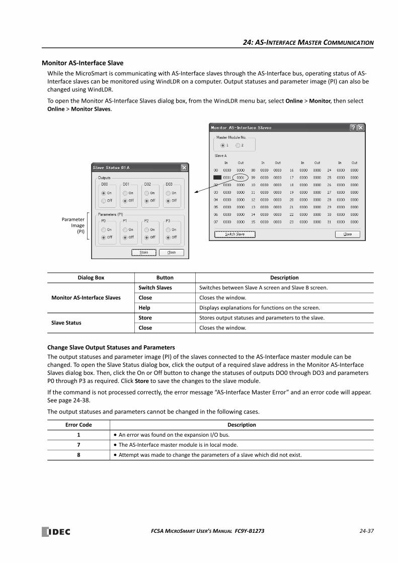
24: AS‐INTERFACE MASTER COMMUNICATION
Monitor AS‐Interface Slave
While the MicroSmart is communicating with AS‐Interface slaves through the AS‐Interface bus, operating status of AS‐Interface slaves can be monitored using WindLDR on a computer. Output statuses and parameter image (PI) can also be changed using WindLDR.
To open the Monitor AS‐Interface Slaves dialog box, from the WindLDR menu bar, select Online > Monitor, then select Online > Monitor Slaves.
Change Slave Output Statuses and Parameters
The output statuses and parameter image (PI) of the slaves connected to the AS‐Interface master module can be changed. To open the Slave Status dialog box, click the output of a required slave address in the Monitor AS‐Interface Slaves dialog box. Then, click the On or Off button to change the statuses of outputs DO0 through DO3 and parameters P0 through P3 as required. Click Store to save the changes to the slave module.
If the command is not processed correctly, the error message “AS‐Interface Master Error” and an error code will appear. See page 24‐38.
The output statuses and parameters cannot be changed in the following cases.
Dialog Box Button Description
Monitor AS‐Interface Slaves
Switch Slaves Switches between Slave A screen and Slave B screen.
Close Closes the window.
Help Displays explanations for functions on the screen.
Slave StatusStore Stores output statuses and parameters to the slave.
Close Closes the window.
Error Code Description
1 An error was found on the expansion I/O bus.
7 The AS‐Interface master module is in local mode.
8 Attempt was made to change the parameters of a slave which did not exist.
ParameterImage
(PI)
FC5A MICROSMART USER’S MANUAL FC9Y‐B1273 24‐37

24: AS‐INTERFACE MASTER COMMUNICATION
Error Messages
When an error is returned from the AS‐Interface master module, WindLDR will display an error message. The error codes and their meanings are given below.
When a reply message is not returned from the AS‐Interface master module, the following error message will be dis‐played.
Error Code Description
1 An error was found on the expansion I/O bus.
2 While the AS‐Interface master module was in offline mode, attempt was made to perform auto config‐uration or manual configuration.
An incorrect command was sent.
7 While slave address 0 existed on the bus, attempt was made to perform auto configuration or manual configuration.
The AS‐Interface master module is in local mode.
8
The slave you are trying to change does not exist. A slave of the designated new address already exists. While a standard slave was set at A address, attempt was made to set an A/B slave at B address of the same number.
While an A/B slave was set at B address, attempt was made to set a standard slave at A address of the same number.
Attempt was made to change the parameters of a slave which did not exist.
24‐38 FC5A MICROSMART USER’S MANUAL FC9Y‐B1273
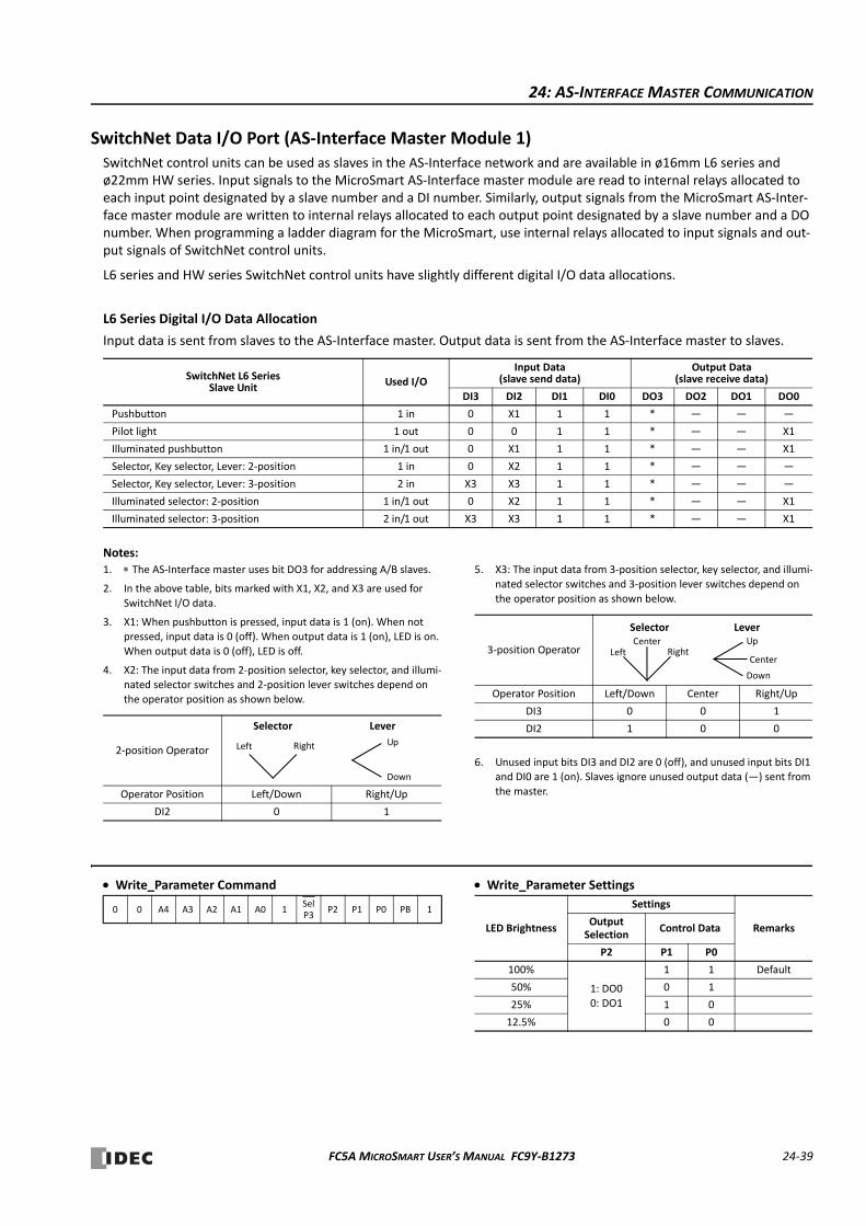
24: AS‐INTERFACE MASTER COMMUNICATION
SwitchNet Data I/O Port (AS‐Interface Master Module 1)SwitchNet control units can be used as slaves in the AS‐Interface network and are available in ø16mm L6 series and ø22mm HW series. Input signals to the MicroSmart AS‐Interface master module are read to internal relays allocated to each input point designated by a slave number and a DI number. Similarly, output signals from the MicroSmart AS‐Inter‐face master module are written to internal relays allocated to each output point designated by a slave number and a DO number. When programming a ladder diagram for the MicroSmart, use internal relays allocated to input signals and out‐put signals of SwitchNet control units.
L6 series and HW series SwitchNet control units have slightly different digital I/O data allocations.
L6 Series Digital I/O Data Allocation
Input data is sent from slaves to the AS‐Interface master. Output data is sent from the AS‐Interface master to slaves.
Notes:
SwitchNet L6 SeriesSlave Unit
Used I/O
Input Data(slave send data)
Output Data(slave receive data)
DI3 DI2 DI1 DI0 DO3 DO2 DO1 DO0
Pushbutton 1 in 0 X1 1 1 * — — —
Pilot light 1 out 0 0 1 1 * — — X1
Illuminated pushbutton 1 in/1 out 0 X1 1 1 * — — X1
Selector, Key selector, Lever: 2‐position 1 in 0 X2 1 1 * — — —
Selector, Key selector, Lever: 3‐position 2 in X3 X3 1 1 * — — —
Illuminated selector: 2‐position 1 in/1 out 0 X2 1 1 * — — X1
Illuminated selector: 3‐position 2 in/1 out X3 X3 1 1 * — — X1
1. The AS‐Interface master uses bit DO3 for addressing A/B slaves.
2. In the above table, bits marked with X1, X2, and X3 are used for
SwitchNet I/O data.
3. X1: When pushbutton is pressed, input data is 1 (on). When not
pressed, input data is 0 (off). When output data is 1 (on), LED is on.
When output data is 0 (off), LED is off.
4. X2: The input data from 2‐position selector, key selector, and illumi‐
nated selector switches and 2‐position lever switches depend on
the operator position as shown below.
5. X3: The input data from 3‐position selector, key selector, and illumi‐
nated selector switches and 3‐position lever switches depend on
the operator position as shown below.
6. Unused input bits DI3 and DI2 are 0 (off), and unused input bits DI1 and DI0 are 1 (on). Slaves ignore unused output data (—) sent from
the master.
2‐position Operator
Operator Position Left/Down Right/Up
DI2 0 1
Selector
Left Right Up
Down
Lever
3‐position Operator
Operator Position Left/Down Center Right/Up
DI3 0 0 1
DI2 1 0 0
Selector
Left RightCenter Up
Center
Down
Lever
Write_Parameter Command Write_Parameter Settings
0 0 A4 A3 A2 A1 A0 1SelP3
P2 P1 P0 PB 1
LED Brightness
Settings
RemarksOutput Selection
Control Data
P2 P1 P0
100%
1: DO00: DO1
1 1 Default
50% 0 1
25% 1 0
12.5% 0 0
FC5A MICROSMART USER’S MANUAL FC9Y‐B1273 24‐39
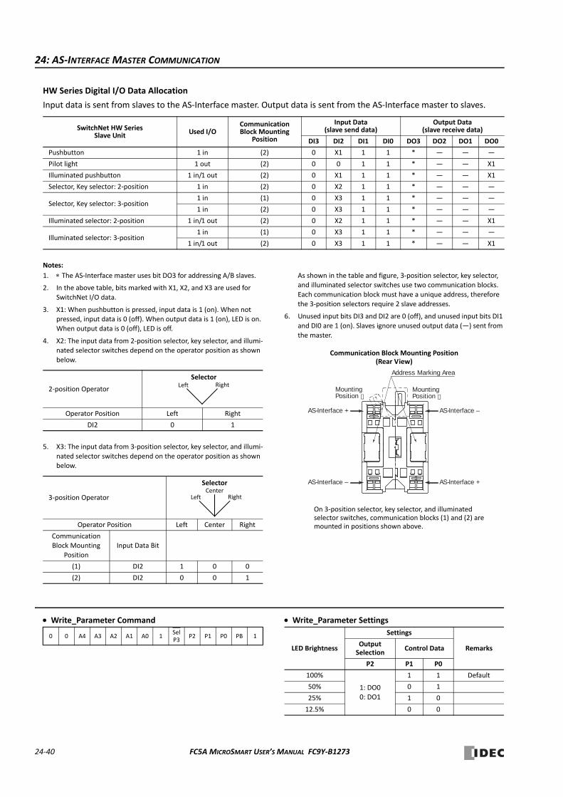
24: AS‐INTERFACE MASTER COMMUNICATION
HW Series Digital I/O Data Allocation
Input data is sent from slaves to the AS‐Interface master. Output data is sent from the AS‐Interface master to slaves.
Notes:
SwitchNet HW SeriesSlave Unit
Used I/OCommunication Block Mounting
Position
Input Data(slave send data)
Output Data(slave receive data)
DI3 DI2 DI1 DI0 DO3 DO2 DO1 DO0
Pushbutton 1 in (2) 0 X1 1 1 * — — —
Pilot light 1 out (2) 0 0 1 1 * — — X1
Illuminated pushbutton 1 in/1 out (2) 0 X1 1 1 * — — X1
Selector, Key selector: 2‐position 1 in (2) 0 X2 1 1 * — — —
Selector, Key selector: 3‐position1 in (1) 0 X3 1 1 * — — —
1 in (2) 0 X3 1 1 * — — —
Illuminated selector: 2‐position 1 in/1 out (2) 0 X2 1 1 * — — X1
Illuminated selector: 3‐position1 in (1) 0 X3 1 1 * — — —
1 in/1 out (2) 0 X3 1 1 * — — X1
1. The AS‐Interface master uses bit DO3 for addressing A/B slaves.
2. In the above table, bits marked with X1, X2, and X3 are used for
SwitchNet I/O data.
3. X1: When pushbutton is pressed, input data is 1 (on). When not pressed, input data is 0 (off). When output data is 1 (on), LED is on.
When output data is 0 (off), LED is off.
4. X2: The input data from 2‐position selector, key selector, and illumi‐nated selector switches depend on the operator position as shown
below.
5. X3: The input data from 3‐position selector, key selector, and illumi‐
nated selector switches depend on the operator position as shown below.
As shown in the table and figure, 3‐position selector, key selector, and illuminated selector switches use two communication blocks.
Each communication block must have a unique address, therefore
the 3‐position selectors require 2 slave addresses.
6. Unused input bits DI3 and DI2 are 0 (off), and unused input bits DI1
and DI0 are 1 (on). Slaves ignore unused output data (—) sent from
the master.
2‐position Operator
Operator Position Left Right
DI2 0 1
3‐position Operator
Operator Position Left Center Right
Communication Block Mounting
Position
Input Data Bit
(1) DI2 1 0 0
(2) DI2 0 0 1
SelectorLeft Right
Selector
Left RightCenter
Address Marking Area
MountingPosition ➀
MountingPosition ➁
AS-Interface –
AS-Interface +
AS-Interface +
AS-Interface –
Communication Block Mounting Position(Rear View)
On 3‐position selector, key selector, and illuminated selector switches, communication blocks (1) and (2) are mounted in positions shown above.
Write_Parameter Command Write_Parameter Settings
0 0 A4 A3 A2 A1 A0 1SelP3
P2 P1 P0 PB 1
LED Brightness
Settings
RemarksOutput Selection
Control Data
P2 P1 P0
100%
1: DO00: DO1
1 1 Default
50% 0 1
25% 1 0
12.5% 0 0
24‐40 FC5A MICROSMART USER’S MANUAL FC9Y‐B1273

24: AS‐INTERFACE MASTER COMMUNICATION
•Internal Relays for SwitchNet Slaves (AS‐Interface Master Module 1)
L6 Series
Slave NumberPushbutton Pilot Light Illuminated Pushbutton
Selector, Key selector, Lever: 2‐position
Input DI2 Output DO0 Input DI2 Output DO0 Input DI2
(Slave 0) M1302 M1620 M1302 M1620 M1302
Slave 1(A) M1306 M1624 M1306 M1624 M1306
Slave 2(A) M1312 M1630 M1312 M1630 M1312
Slave 3(A) M1316 M1634 M1316 M1634 M1316
Slave 4(A) M1322 M1640 M1322 M1640 M1322
Slave 5(A) M1326 M1644 M1326 M1644 M1326
Slave 6(A) M1332 M1650 M1332 M1650 M1332
Slave 7(A) M1336 M1654 M1336 M1654 M1336
Slave 8(A) M1342 M1660 M1342 M1660 M1342
Slave 9(A) M1346 M1664 M1346 M1664 M1346
Slave 10(A) M1352 M1670 M1352 M1670 M1352
Slave 11(A) M1356 M1674 M1356 M1674 M1356
Slave 12(A) M1362 M1680 M1362 M1680 M1362
Slave 13(A) M1366 M1684 M1366 M1684 M1366
Slave 14(A) M1372 M1690 M1372 M1690 M1372
Slave 15(A) M1376 M1694 M1376 M1694 M1376
Slave 16(A) M1382 M1700 M1382 M1700 M1382
Slave 17(A) M1386 M1704 M1386 M1704 M1386
Slave 18(A) M1392 M1710 M1392 M1710 M1392
Slave 19(A) M1396 M1714 M1396 M1714 M1396
Slave 20(A) M1402 M1720 M1402 M1720 M1402
Slave 21(A) M1406 M1724 M1406 M1724 M1406
Slave 22(A) M1412 M1730 M1412 M1730 M1412
Slave 23(A) M1416 M1734 M1416 M1734 M1416
Slave 24(A) M1422 M1740 M1422 M1740 M1422
Slave 25(A) M1426 M1744 M1426 M1744 M1426
Slave 26(A) M1432 M1750 M1432 M1750 M1432
Slave 27(A) M1436 M1754 M1436 M1754 M1436
Slave 28(A) M1442 M1760 M1442 M1760 M1442
Slave 29(A) M1446 M1764 M1446 M1764 M1446
Slave 30(A) M1452 M1770 M1452 M1770 M1452
Slave 31(A) M1456 M1774 M1456 M1774 M1456
Slave 1B M1466 M1784 M1466 M1784 M1466
Slave 2B M1472 M1790 M1472 M1790 M1472
Slave 3B M1476 M1794 M1476 M1794 M1476
Slave 4B M1482 M1800 M1482 M1800 M1482
Slave 5B M1486 M1804 M1486 M1804 M1486
Slave 6B M1492 M1810 M1492 M1810 M1492
Slave 7B M1496 M1814 M1496 M1814 M1496
Slave 8B M1502 M1820 M1502 M1820 M1502
Slave 9B M1506 M1824 M1506 M1824 M1506
Slave 10B M1512 M1830 M1512 M1830 M1512
Slave 11B M1516 M1834 M1516 M1834 M1516
Slave 12B M1522 M1840 M1522 M1840 M1522
Slave 13B M1526 M1844 M1526 M1844 M1526
Slave 14B M1532 M1850 M1532 M1850 M1532
Slave 15B M1536 M1854 M1536 M1854 M1536
Slave 16B M1542 M1860 M1542 M1860 M1542
Slave 17B M1546 M1864 M1546 M1864 M1546
Slave 18B M1552 M1870 M1552 M1870 M1552
Slave 19B M1556 M1874 M1556 M1874 M1556
Slave 20B M1562 M1880 M1562 M1880 M1562
Slave 21B M1566 M1884 M1566 M1884 M1566
Slave 22B M1572 M1890 M1572 M1890 M1572
Slave 23B M1576 M1894 M1576 M1894 M1576
Slave 24B M1582 M1900 M1582 M1900 M1582
Slave 25B M1586 M1904 M1586 M1904 M1586
Slave 26B M1592 M1910 M1592 M1910 M1592
Slave 27B M1596 M1914 M1596 M1914 M1596
Slave 28B M1602 M1920 M1602 M1920 M1602
Slave 29B M1606 M1924 M1606 M1924 M1606
Slave 30B M1612 M1930 M1612 M1930 M1612
Slave 31B M1616 M1934 M1616 M1934 M1616
FC5A MICROSMART USER’S MANUAL FC9Y‐B1273 24‐41
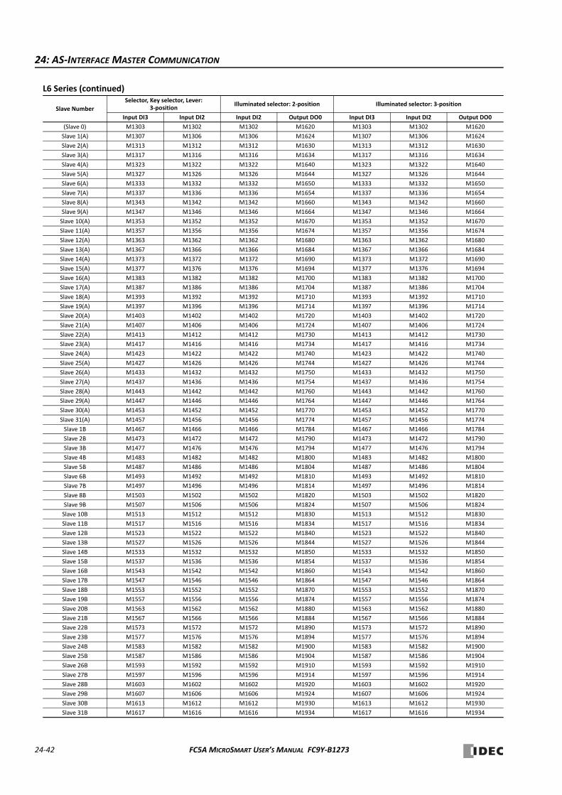
24: AS‐INTERFACE MASTER COMMUNICATION
L6 Series (continued)
Slave Number
Selector, Key selector, Lever: 3‐position
Illuminated selector: 2‐position Illuminated selector: 3‐position
Input DI3 Input DI2 Input DI2 Output DO0 Input DI3 Input DI2 Output DO0
(Slave 0) M1303 M1302 M1302 M1620 M1303 M1302 M1620
Slave 1(A) M1307 M1306 M1306 M1624 M1307 M1306 M1624
Slave 2(A) M1313 M1312 M1312 M1630 M1313 M1312 M1630
Slave 3(A) M1317 M1316 M1316 M1634 M1317 M1316 M1634
Slave 4(A) M1323 M1322 M1322 M1640 M1323 M1322 M1640
Slave 5(A) M1327 M1326 M1326 M1644 M1327 M1326 M1644
Slave 6(A) M1333 M1332 M1332 M1650 M1333 M1332 M1650
Slave 7(A) M1337 M1336 M1336 M1654 M1337 M1336 M1654
Slave 8(A) M1343 M1342 M1342 M1660 M1343 M1342 M1660
Slave 9(A) M1347 M1346 M1346 M1664 M1347 M1346 M1664
Slave 10(A) M1353 M1352 M1352 M1670 M1353 M1352 M1670
Slave 11(A) M1357 M1356 M1356 M1674 M1357 M1356 M1674
Slave 12(A) M1363 M1362 M1362 M1680 M1363 M1362 M1680
Slave 13(A) M1367 M1366 M1366 M1684 M1367 M1366 M1684
Slave 14(A) M1373 M1372 M1372 M1690 M1373 M1372 M1690
Slave 15(A) M1377 M1376 M1376 M1694 M1377 M1376 M1694
Slave 16(A) M1383 M1382 M1382 M1700 M1383 M1382 M1700
Slave 17(A) M1387 M1386 M1386 M1704 M1387 M1386 M1704
Slave 18(A) M1393 M1392 M1392 M1710 M1393 M1392 M1710
Slave 19(A) M1397 M1396 M1396 M1714 M1397 M1396 M1714
Slave 20(A) M1403 M1402 M1402 M1720 M1403 M1402 M1720
Slave 21(A) M1407 M1406 M1406 M1724 M1407 M1406 M1724
Slave 22(A) M1413 M1412 M1412 M1730 M1413 M1412 M1730
Slave 23(A) M1417 M1416 M1416 M1734 M1417 M1416 M1734
Slave 24(A) M1423 M1422 M1422 M1740 M1423 M1422 M1740
Slave 25(A) M1427 M1426 M1426 M1744 M1427 M1426 M1744
Slave 26(A) M1433 M1432 M1432 M1750 M1433 M1432 M1750
Slave 27(A) M1437 M1436 M1436 M1754 M1437 M1436 M1754
Slave 28(A) M1443 M1442 M1442 M1760 M1443 M1442 M1760
Slave 29(A) M1447 M1446 M1446 M1764 M1447 M1446 M1764
Slave 30(A) M1453 M1452 M1452 M1770 M1453 M1452 M1770
Slave 31(A) M1457 M1456 M1456 M1774 M1457 M1456 M1774
Slave 1B M1467 M1466 M1466 M1784 M1467 M1466 M1784
Slave 2B M1473 M1472 M1472 M1790 M1473 M1472 M1790
Slave 3B M1477 M1476 M1476 M1794 M1477 M1476 M1794
Slave 4B M1483 M1482 M1482 M1800 M1483 M1482 M1800
Slave 5B M1487 M1486 M1486 M1804 M1487 M1486 M1804
Slave 6B M1493 M1492 M1492 M1810 M1493 M1492 M1810
Slave 7B M1497 M1496 M1496 M1814 M1497 M1496 M1814
Slave 8B M1503 M1502 M1502 M1820 M1503 M1502 M1820
Slave 9B M1507 M1506 M1506 M1824 M1507 M1506 M1824
Slave 10B M1513 M1512 M1512 M1830 M1513 M1512 M1830
Slave 11B M1517 M1516 M1516 M1834 M1517 M1516 M1834
Slave 12B M1523 M1522 M1522 M1840 M1523 M1522 M1840
Slave 13B M1527 M1526 M1526 M1844 M1527 M1526 M1844
Slave 14B M1533 M1532 M1532 M1850 M1533 M1532 M1850
Slave 15B M1537 M1536 M1536 M1854 M1537 M1536 M1854
Slave 16B M1543 M1542 M1542 M1860 M1543 M1542 M1860
Slave 17B M1547 M1546 M1546 M1864 M1547 M1546 M1864
Slave 18B M1553 M1552 M1552 M1870 M1553 M1552 M1870
Slave 19B M1557 M1556 M1556 M1874 M1557 M1556 M1874
Slave 20B M1563 M1562 M1562 M1880 M1563 M1562 M1880
Slave 21B M1567 M1566 M1566 M1884 M1567 M1566 M1884
Slave 22B M1573 M1572 M1572 M1890 M1573 M1572 M1890
Slave 23B M1577 M1576 M1576 M1894 M1577 M1576 M1894
Slave 24B M1583 M1582 M1582 M1900 M1583 M1582 M1900
Slave 25B M1587 M1586 M1586 M1904 M1587 M1586 M1904
Slave 26B M1593 M1592 M1592 M1910 M1593 M1592 M1910
Slave 27B M1597 M1596 M1596 M1914 M1597 M1596 M1914
Slave 28B M1603 M1602 M1602 M1920 M1603 M1602 M1920
Slave 29B M1607 M1606 M1606 M1924 M1607 M1606 M1924
Slave 30B M1613 M1612 M1612 M1930 M1613 M1612 M1930
Slave 31B M1617 M1616 M1616 M1934 M1617 M1616 M1934
24‐42 FC5A MICROSMART USER’S MANUAL FC9Y‐B1273

24: AS‐INTERFACE MASTER COMMUNICATION
HW Series
Slave NumberPushbutton Pilot Light Illuminated Pushbutton
Selector, Key selector:2‐position
Input DI2 Output DO0 Input DI2 Output DO0 Input DI2
(Slave 0) M1302 M1620 M1302 M1620 M1302
Slave 1(A) M1306 M1624 M1306 M1624 M1306
Slave 2(A) M1312 M1630 M1312 M1630 M1312
Slave 3(A) M1316 M1634 M1316 M1634 M1316
Slave 4(A) M1322 M1640 M1322 M1640 M1322
Slave 5(A) M1326 M1644 M1326 M1644 M1326
Slave 6(A) M1332 M1650 M1332 M1650 M1332
Slave 7(A) M1336 M1654 M1336 M1654 M1336
Slave 8(A) M1342 M1660 M1342 M1660 M1342
Slave 9(A) M1346 M1664 M1346 M1664 M1346
Slave 10(A) M1352 M1670 M1352 M1670 M1352
Slave 11(A) M1356 M1674 M1356 M1674 M1356
Slave 12(A) M1362 M1680 M1362 M1680 M1362
Slave 13(A) M1366 M1684 M1366 M1684 M1366
Slave 14(A) M1372 M1690 M1372 M1690 M1372
Slave 15(A) M1376 M1694 M1376 M1694 M1376
Slave 16(A) M1382 M1700 M1382 M1700 M1382
Slave 17(A) M1386 M1704 M1386 M1704 M1386
Slave 18(A) M1392 M1710 M1392 M1710 M1392
Slave 19(A) M1396 M1714 M1396 M1714 M1396
Slave 20(A) M1402 M1720 M1402 M1720 M1402
Slave 21(A) M1406 M1724 M1406 M1724 M1406
Slave 22(A) M1412 M1730 M1412 M1730 M1412
Slave 23(A) M1416 M1734 M1416 M1734 M1416
Slave 24(A) M1422 M1740 M1422 M1740 M1422
Slave 25(A) M1426 M1744 M1426 M1744 M1426
Slave 26(A) M1432 M1750 M1432 M1750 M1432
Slave 27(A) M1436 M1754 M1436 M1754 M1436
Slave 28(A) M1442 M1760 M1442 M1760 M1442
Slave 29(A) M1446 M1764 M1446 M1764 M1446
Slave 30(A) M1452 M1770 M1452 M1770 M1452
Slave 31(A) M1456 M1774 M1456 M1774 M1456
Slave 1B M1466 M1784 M1466 M1784 M1466
Slave 2B M1472 M1790 M1472 M1790 M1472
Slave 3B M1476 M1794 M1476 M1794 M1476
Slave 4B M1482 M1800 M1482 M1800 M1482
Slave 5B M1486 M1804 M1486 M1804 M1486
Slave 6B M1492 M1810 M1492 M1810 M1492
Slave 7B M1496 M1814 M1496 M1814 M1496
Slave 8B M1502 M1820 M1502 M1820 M1502
Slave 9B M1506 M1824 M1506 M1824 M1506
Slave 10B M1512 M1830 M1512 M1830 M1512
Slave 11B M1516 M1834 M1516 M1834 M1516
Slave 12B M1522 M1840 M1522 M1840 M1522
Slave 13B M1526 M1844 M1526 M1844 M1526
Slave 14B M1532 M1850 M1532 M1850 M1532
Slave 15B M1536 M1854 M1536 M1854 M1536
Slave 16B M1542 M1860 M1542 M1860 M1542
Slave 17B M1546 M1864 M1546 M1864 M1546
Slave 18B M1552 M1870 M1552 M1870 M1552
Slave 19B M1556 M1874 M1556 M1874 M1556
Slave 20B M1562 M1880 M1562 M1880 M1562
Slave 21B M1566 M1884 M1566 M1884 M1566
Slave 22B M1572 M1890 M1572 M1890 M1572
Slave 23B M1576 M1894 M1576 M1894 M1576
Slave 24B M1582 M1900 M1582 M1900 M1582
Slave 25B M1586 M1904 M1586 M1904 M1586
Slave 26B M1592 M1910 M1592 M1910 M1592
Slave 27B M1596 M1914 M1596 M1914 M1596
Slave 28B M1602 M1920 M1602 M1920 M1602
Slave 29B M1606 M1924 M1606 M1924 M1606
Slave 30B M1612 M1930 M1612 M1930 M1612
Slave 31B M1616 M1934 M1616 M1934 M1616
FC5A MICROSMART USER’S MANUAL FC9Y‐B1273 24‐43
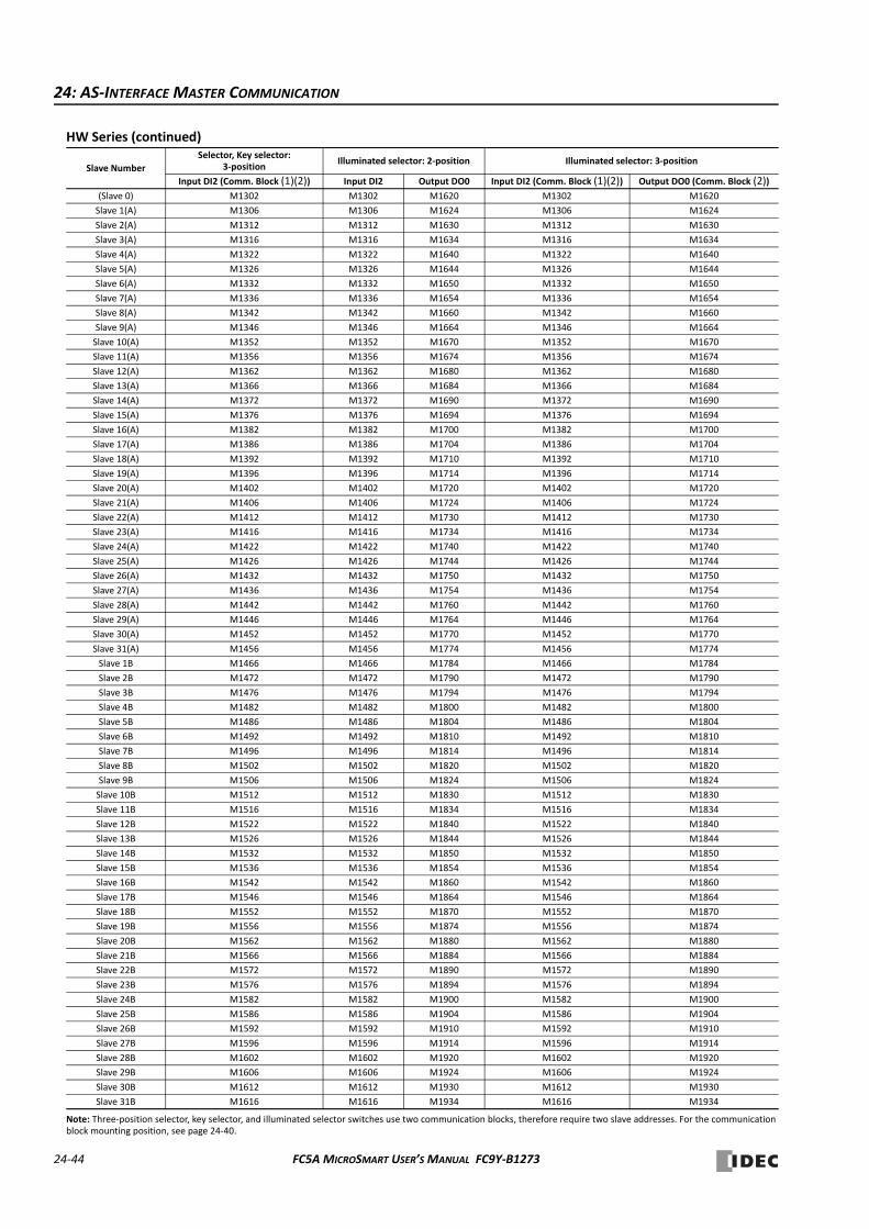
24: AS‐INTERFACE MASTER COMMUNICATION
HW Series (continued)
Note: Three‐position selector, key selector, and illuminated selector switches use two communication blocks, therefore require two slave addresses. For the communication block mounting position, see page 24‐40.
Slave Number
Selector, Key selector: 3‐position
Illuminated selector: 2‐position Illuminated selector: 3‐position
Input DI2 (Comm. Block (1)(2)) Input DI2 Output DO0 Input DI2 (Comm. Block (1)(2)) Output DO0 (Comm. Block (2))
(Slave 0) M1302 M1302 M1620 M1302 M1620
Slave 1(A) M1306 M1306 M1624 M1306 M1624
Slave 2(A) M1312 M1312 M1630 M1312 M1630
Slave 3(A) M1316 M1316 M1634 M1316 M1634
Slave 4(A) M1322 M1322 M1640 M1322 M1640
Slave 5(A) M1326 M1326 M1644 M1326 M1644
Slave 6(A) M1332 M1332 M1650 M1332 M1650
Slave 7(A) M1336 M1336 M1654 M1336 M1654
Slave 8(A) M1342 M1342 M1660 M1342 M1660
Slave 9(A) M1346 M1346 M1664 M1346 M1664
Slave 10(A) M1352 M1352 M1670 M1352 M1670
Slave 11(A) M1356 M1356 M1674 M1356 M1674
Slave 12(A) M1362 M1362 M1680 M1362 M1680
Slave 13(A) M1366 M1366 M1684 M1366 M1684
Slave 14(A) M1372 M1372 M1690 M1372 M1690
Slave 15(A) M1376 M1376 M1694 M1376 M1694
Slave 16(A) M1382 M1382 M1700 M1382 M1700
Slave 17(A) M1386 M1386 M1704 M1386 M1704
Slave 18(A) M1392 M1392 M1710 M1392 M1710
Slave 19(A) M1396 M1396 M1714 M1396 M1714
Slave 20(A) M1402 M1402 M1720 M1402 M1720
Slave 21(A) M1406 M1406 M1724 M1406 M1724
Slave 22(A) M1412 M1412 M1730 M1412 M1730
Slave 23(A) M1416 M1416 M1734 M1416 M1734
Slave 24(A) M1422 M1422 M1740 M1422 M1740
Slave 25(A) M1426 M1426 M1744 M1426 M1744
Slave 26(A) M1432 M1432 M1750 M1432 M1750
Slave 27(A) M1436 M1436 M1754 M1436 M1754
Slave 28(A) M1442 M1442 M1760 M1442 M1760
Slave 29(A) M1446 M1446 M1764 M1446 M1764
Slave 30(A) M1452 M1452 M1770 M1452 M1770
Slave 31(A) M1456 M1456 M1774 M1456 M1774
Slave 1B M1466 M1466 M1784 M1466 M1784
Slave 2B M1472 M1472 M1790 M1472 M1790
Slave 3B M1476 M1476 M1794 M1476 M1794
Slave 4B M1482 M1482 M1800 M1482 M1800
Slave 5B M1486 M1486 M1804 M1486 M1804
Slave 6B M1492 M1492 M1810 M1492 M1810
Slave 7B M1496 M1496 M1814 M1496 M1814
Slave 8B M1502 M1502 M1820 M1502 M1820
Slave 9B M1506 M1506 M1824 M1506 M1824
Slave 10B M1512 M1512 M1830 M1512 M1830
Slave 11B M1516 M1516 M1834 M1516 M1834
Slave 12B M1522 M1522 M1840 M1522 M1840
Slave 13B M1526 M1526 M1844 M1526 M1844
Slave 14B M1532 M1532 M1850 M1532 M1850
Slave 15B M1536 M1536 M1854 M1536 M1854
Slave 16B M1542 M1542 M1860 M1542 M1860
Slave 17B M1546 M1546 M1864 M1546 M1864
Slave 18B M1552 M1552 M1870 M1552 M1870
Slave 19B M1556 M1556 M1874 M1556 M1874
Slave 20B M1562 M1562 M1880 M1562 M1880
Slave 21B M1566 M1566 M1884 M1566 M1884
Slave 22B M1572 M1572 M1890 M1572 M1890
Slave 23B M1576 M1576 M1894 M1576 M1894
Slave 24B M1582 M1582 M1900 M1582 M1900
Slave 25B M1586 M1586 M1904 M1586 M1904
Slave 26B M1592 M1592 M1910 M1592 M1910
Slave 27B M1596 M1596 M1914 M1596 M1914
Slave 28B M1602 M1602 M1920 M1602 M1920
Slave 29B M1606 M1606 M1924 M1606 M1924
Slave 30B M1612 M1612 M1930 M1612 M1930
Slave 31B M1616 M1616 M1934 M1616 M1934
24‐44 FC5A MICROSMART USER’S MANUAL FC9Y‐B1273
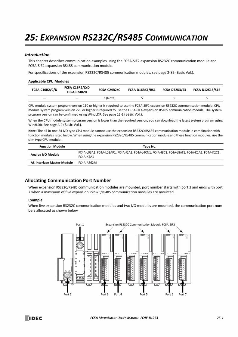
25: EXPANSION RS232C/RS485 COMMUNICATION
IntroductionThis chapter describes communication examples using the FC5A‐SIF2 expansion RS232C communication module and FC5A‐SIF4 expansion RS485 communication module.
For specifications of the expansion RS232C/RS485 communication modules, see page 2‐86 (Basic Vol.).
Applicable CPU Modules
CPU module system program version 110 or higher is required to use the FC5A‐SIF2 expansion RS232C communication module. CPU module system program version 220 or higher is required to use the FC5A‐SIF4 expansion RS485 communication module. The system program version can be confirmed using WindLDR. See page 13‐2 (Basic Vol.).
When the CPU module system program version is lower than the required version, you can download the latest system program using WindLDR. See page A‐9 (Basic Vol.).
Note: The all‐in‐one 24‐I/O type CPU module cannot use the expansion RS232C/RS485 communication module in combination with function modules listed below. When using the expansion RS232C/RS485 communication module and these function modules, use the slim type CPU module.
Allocating Communication Port NumberWhen expansion RS232C/RS485 communication modules are mounted, port number starts with port 3 and ends with port 7 when a maximum of five expansion RS232C/RS485 communication modules are mounted.
Example:
When five expansion RS232C communication modules and two I/O modules are mounted, the communication port num‐bers allocated as shown below.
FC5A‐C10R2/C/DFC5A‐C16R2/C/DFC5A‐C24R2D
FC5A‐C24R2/C FC5A‐D16RK1/RS1 FC5A‐D32K3/S3 FC5A‐D12K1E/S1E
— — 3 (Note) 5 5 5
Function Module Type No.
Analog I/O ModuleFC4A‐L03A1, FC4A‐L03AP1, FC4A‐J2A1, FC4A‐J4CN1, FC4A‐J8C1, FC4A‐J8AT1, FC4A‐K1A1, FC4A‐K2C1, FC4A‐K4A1
AS‐Interface Master Module FC4A‐AS62M
PWRSDRD
RS232C
RS
ER
SD
RD
DR
SG
NC
PWRSDRD
RS232C
RS
ER
SD
RD
DR
SG
NC
PWRSDRD
RS232C
RS
ER
SD
RD
DR
SG
NC
PWRSDRD
RS232C
RS
ER
SD
RD
DR
SG
NC
PWRSDRD
RS232C
RS
ER
SD
RD
DR
SG
NC
Port 2 Port 3 Port 4 Port 5 Port 6 Port 7
Port 1 Expansion RS232C Communication Module FC5A‐SIF2
FC5A MICROSMART USER’S MANUAL FC9Y‐B1273 25‐1

25: EXPANSION RS232C/RS485 COMMUNICATION
Computer Link CommunicationThe computer link communication can be used with WindLDR on a PC connected to the CPU module to perform mainte‐nance operations, such as download/upload user programs, start/stop the PLC, monitor the PLC status, and read/write device values. When the expansion RS232C/RS485 communication module is mounted to the CPU module in a computer link system, the computer link communication functions can be performed, except for Run‐Time Program Download. For details about the computer link communication, see pages 4‐1 (Basic Vol.) and 21‐1.
System Setup Example
Cable Connection and Pinouts (FC5A‐SIF2 Expansion RS232C Communication Module)
+ Ð24VDC
PWRSDRD
RS232C
RS
ER
SD
RD
DR
SG
NC
Computer Link Cable 4CFC2A‐KC4C3m (9.84 ft.) long
To Port 3 (RS232C)
To Port 1 (RS232C)
CPU Module
The communication cable is prepared by the user refer‐ring to the diagram shown below. For the wiring precautions, see page 2‐89 (Basic Vol.).
Expansion RS232C Communication ModuleFC5A‐SIF2
Note: Run‐Time Program Download cannot be used through the expansion RS232C/RS485 communication module.Note: When expansion RS485 communication module is used, connect a PC and the CPU module using a USB/RS485 converter from third party.
Computer (D‐sub 9‐pin)
Pin Description
8 CS
3 SD
2 RD
4 ER
6 DR
1 CD
5 SG
Cover FG
7 RS
9 RI
FC5A‐SIF2
Terminal
RS (RTS)
ER (DTR)
SD (TXD)
RD (RXD)
DR (DSR)
SG (SG)
NC
Shield
25‐2 FC5A MICROSMART USER’S MANUAL FC9Y‐B1273
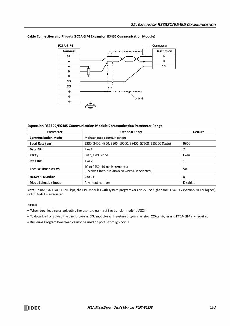
25: EXPANSION RS232C/RS485 COMMUNICATION
Cable Connection and Pinouts (FC5A‐SIF4 Expansion RS485 Communication Module)
Expansion RS232C/RS485 Communication Module Communication Parameter Range
Note: To use 57600 or 115200 bps, the CPU modules with system program version 220 or higher and FC5A‐SIF2 (version 200 or higher) or FC5A‐SIF4 are required.
Notes:
When downloading or uploading the user program, set the transfer mode to ASCII.
To download or upload the user program, CPU modules with system program version 220 or higher and FC5A‐SIF4 are required.
Run‐Time Program Download cannot be used on port 3 through port 7.
Parameter Optional Range Default
Communication Mode Maintenance communication
Baud Rate (bps) 1200, 2400, 4800, 9600, 19200, 38400, 57600, 115200 (Note) 9600
Data Bits 7 or 8 7
Parity Even, Odd, None Even
Stop Bits 1 or 2 1
Receive Timeout (ms)10 to 2550 (10‐ms increments)(Receive timeout is disabled when 0 is selected.)
500
Network Number 0 to 31 0
Mode Selection Input Any input number Disabled
Computer
Description
A
B
SG
FC5A‐SIF4
Terminal
NC
A
A
B
B
SG
SG
Shield
FC5A MICROSMART USER’S MANUAL FC9Y‐B1273 25‐3
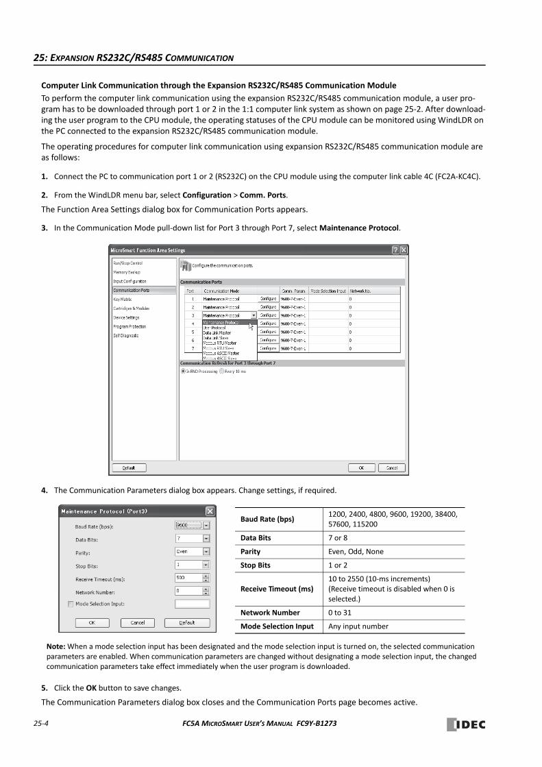
25: EXPANSION RS232C/RS485 COMMUNICATION
Computer Link Communication through the Expansion RS232C/RS485 Communication Module
To perform the computer link communication using the expansion RS232C/RS485 communication module, a user pro‐gram has to be downloaded through port 1 or 2 in the 1:1 computer link system as shown on page 25‐2. After download‐ing the user program to the CPU module, the operating statuses of the CPU module can be monitored using WindLDR on the PC connected to the expansion RS232C/RS485 communication module.
The operating procedures for computer link communication using expansion RS232C/RS485 communication module are as follows:
1. Connect the PC to communication port 1 or 2 (RS232C) on the CPU module using the computer link cable 4C (FC2A‐KC4C).
2. From the WindLDR menu bar, select Configuration > Comm. Ports.
The Function Area Settings dialog box for Communication Ports appears.
3. In the Communication Mode pull‐down list for Port 3 through Port 7, select Maintenance Protocol.
4. The Communication Parameters dialog box appears. Change settings, if required.
5. Click the OK button to save changes.
The Communication Parameters dialog box closes and the Communication Ports page becomes active.
Baud Rate (bps)1200, 2400, 4800, 9600, 19200, 38400, 57600, 115200
Data Bits 7 or 8
Parity Even, Odd, None
Stop Bits 1 or 2
Receive Timeout (ms)10 to 2550 (10‐ms increments)(Receive timeout is disabled when 0 is selected.)
Network Number 0 to 31
Mode Selection Input Any input number
Note: When a mode selection input has been designated and the mode selection input is turned on, the selected communication parameters are enabled. When communication parameters are changed without designating a mode selection input, the changed communication parameters take effect immediately when the user program is downloaded.
25‐4 FC5A MICROSMART USER’S MANUAL FC9Y‐B1273
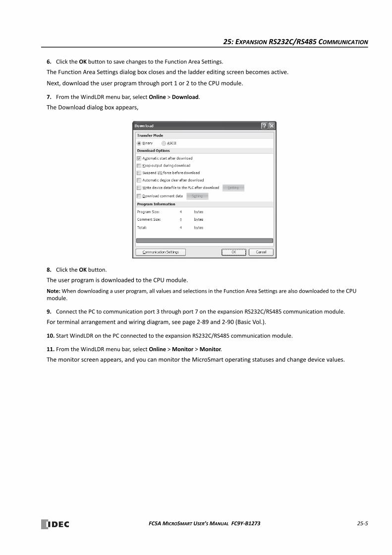
25: EXPANSION RS232C/RS485 COMMUNICATION
6. Click the OK button to save changes to the Function Area Settings.
The Function Area Settings dialog box closes and the ladder editing screen becomes active.
Next, download the user program through port 1 or 2 to the CPU module.
7. From the WindLDR menu bar, select Online > Download.
The Download dialog box appears,
8. Click the OK button.
The user program is downloaded to the CPU module.
Note: When downloading a user program, all values and selections in the Function Area Settings are also downloaded to the CPU module.
9. Connect the PC to communication port 3 through port 7 on the expansion RS232C/RS485 communication module.
For terminal arrangement and wiring diagram, see page 2‐89 and 2‐90 (Basic Vol.).
10. Start WindLDR on the PC connected to the expansion RS232C/RS485 communication module.
11. From the WindLDR menu bar, select Online > Monitor > Monitor.
The monitor screen appears, and you can monitor the MicroSmart operating statuses and change device values.
FC5A MICROSMART USER’S MANUAL FC9Y‐B1273 25‐5
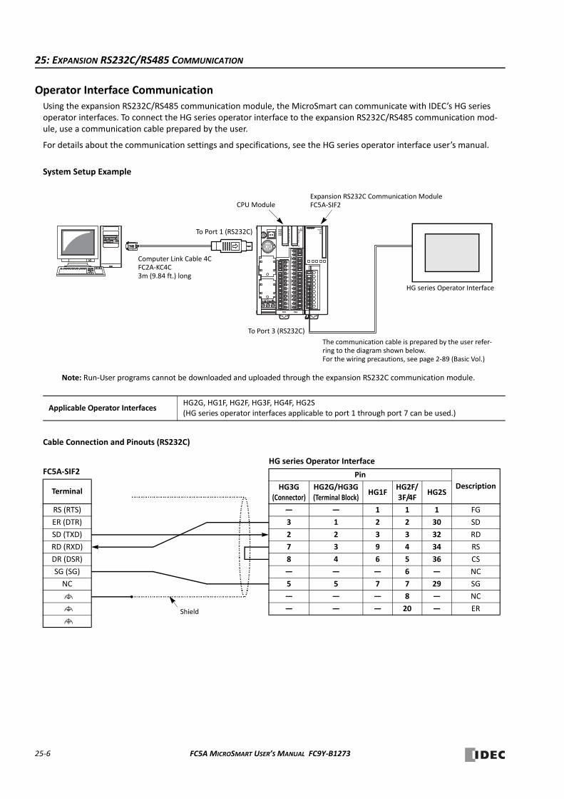
25: EXPANSION RS232C/RS485 COMMUNICATION
Operator Interface CommunicationUsing the expansion RS232C/RS485 communication module, the MicroSmart can communicate with IDEC’s HG series operator interfaces. To connect the HG series operator interface to the expansion RS232C/RS485 communication mod‐ule, use a communication cable prepared by the user.
For details about the communication settings and specifications, see the HG series operator interface user’s manual.
System Setup Example
Cable Connection and Pinouts (RS232C)
Applicable Operator InterfacesHG2G, HG1F, HG2F, HG3F, HG4F, HG2S(HG series operator interfaces applicable to port 1 through port 7 can be used.)
+ Ð24VDC NC
NC
PWRSDRD
RS232C
RS
ER
SD
RD
DR
SG
NC
NC
Computer Link Cable 4CFC2A‐KC4C3m (9.84 ft.) long
To Port 3 (RS232C)
To Port 1 (RS232C)
CPU Module
The communication cable is prepared by the user refer‐ring to the diagram shown below. For the wiring precautions, see page 2‐89 (Basic Vol.)
Expansion RS232C Communication ModuleFC5A‐SIF2
Note: Run‐User programs cannot be downloaded and uploaded through the expansion RS232C communication module.
HG series Operator Interface
HG series Operator Interface
Pin
DescriptionHG3G(Connector)
HG2G/HG3G(Terminal Block)
HG1FHG2F/3F/4F
HG2S
— — 1 1 1 FG
3 1 2 2 30 SD
2 2 3 3 32 RD
7 3 9 4 34 RS
8 4 6 5 36 CS
— — — 6 — NC
5 5 7 7 29 SG
— — — 8 — NC
— — — 20 — ER
FC5A‐SIF2
Terminal
RS (RTS)
ER (DTR)
SD (TXD)
RD (RXD)
DR (DSR)
SG (SG)
NC
Shield
25‐6 FC5A MICROSMART USER’S MANUAL FC9Y‐B1273
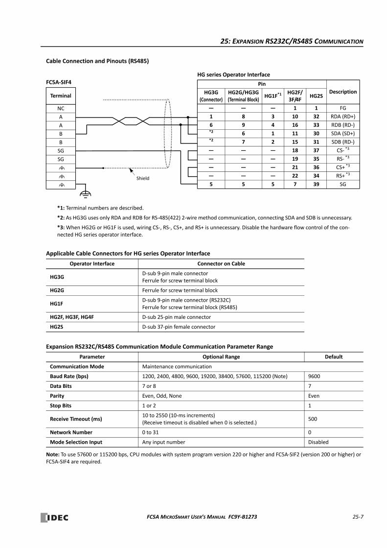
25: EXPANSION RS232C/RS485 COMMUNICATION
Cable Connection and Pinouts (RS485)
Applicable Cable Connectors for HG series Operator Interface
Expansion RS232C/RS485 Communication Module Communication Parameter Range
Note: To use 57600 or 115200 bps, CPU modules with system program version 220 or higher and FC5A‐SIF2 (version 200 or higher) or FC5A‐SIF4 are required.
Operator Interface Connector on Cable
HG3GD‐sub 9‐pin male connectorFerrule for screw terminal block
HG2G Ferrule for screw terminal block
HG1FD‐sub 9‐pin male connector (RS232C)Ferrule for screw terminal block (RS485)
HG2F, HG3F, HG4F D‐sub 25‐pin male connector
HG2S D‐sub 37‐pin female connector
Parameter Optional Range Default
Communication Mode Maintenance communication
Baud Rate (bps) 1200, 2400, 4800, 9600, 19200, 38400, 57600, 115200 (Note) 9600
Data Bits 7 or 8 7
Parity Even, Odd, None Even
Stop Bits 1 or 2 1
Receive Timeout (ms)10 to 2550 (10‐ms increments)(Receive timeout is disabled when 0 is selected.)
500
Network Number 0 to 31 0
Mode Selection Input Any input number Disabled
HG series Operator Interface
Pin
DescriptionHG3G(Connector)
HG2G/HG3G(Terminal Block)
HG1F*1HG2F/3F/4F
HG2S
— — — 1 1 FG
1 8 3 10 32 RDA (RD+)
6 9 4 16 33 RDB (RD‐)*2 6 1 11 30 SDA (SD+)*2 7 2 15 31 SDB (RD‐)
— — — 18 37 CS‐ *3
— — — 19 35 RS‐ *3
— — — 21 36 CS+ *3
— — — 22 34 RS+ *3
5 5 5 7 39 SG
FC5A‐SIF4
Terminal
NC
A
A
B
B
SG
SG
Shield
*1: Terminal numbers are described.
*2: As HG3G uses only RDA and RDB for RS‐485(422) 2‐wire method communication, connecting SDA and SDB is unnecessary.
*3: When HG2G or HG1F is used, wiring CS‐, RS‐, CS+, and RS+ is unnecessary. Disable the hardware flow control of the con‐nected HG series operator interface.
FC5A MICROSMART USER’S MANUAL FC9Y‐B1273 25‐7
25: EXPANSION RS232C/RS485 COMMUNICATION
Operator Interface Communication through the Expansion RS232C/RS485 Communication Module
To perform the operator interface communication using the expansion RS232C/RS485 communication module, a user program has to be downloaded through port 1 or 2 in the 1:1 computer link system as shown on page 25‐6. After down‐loading the user program to the CPU module, the CPU module can communicate with the operator interface through the expansion RS232C/RS485 communication module.
The operating procedures for operator interface communication are as follows:
1. Change the Function Area Settings, if required, and download the user program through communication port 1 or 2 (RS232C) on the CPU module. See step 1 through step 8 shown on pages 25‐4 and 25‐5.
2. Connect the operator interface to communication port 3 through port 7 on the expansion RS232C/RS485 communication module.
For terminal arrangement and wiring diagram, see page 2‐89 and 2‐90 (Basic Vol.).
Now the CPU module can communicate with the operator interface using communication port 3 through port 7.
Note: When the refreshing cycle of display data on the operator interface is slow, see “Communication response is slow” on page 25‐13.
25‐8 FC5A MICROSMART USER’S MANUAL FC9Y‐B1273
25: EXPANSION RS232C/RS485 COMMUNICATION
User CommunicationThe user communication function can be used for the MicroSmart to communicate with a PC, printer, and barcode reader through the expansion RS232C/RS485 communication module. For details about the user communication function, see page 10‐1 (Basic Vol.).
Expansion RS232C/RS485 Communication Module Communication Parameter Range
Note: To use 57600 or 115200 bps, CPU modules with system program version 220 or higher and FC5A‐SIF2 (version 200 or higher) or FC5A‐SIF4 are required.
User Communication through the Expansion RS232C Communication Module
This section describes an example of user communication through the expansion RS232C communication module to send data to a printer. After downloading the user program to the CPU module, the CPU module can communicate with the printer through the expansion RS232C communication module.
The operating procedures for user communication are as follows:
1. Change the Function Area Settings, if required, and download the user program through communication port 1 or 2 (RS232C) on the CPU module. See step 1 through step 8 shown on pages 25‐4 and 25‐5.
2. Connect the printer to communication port 3 through port 7 on the expansion RS232C communication module.
For terminal arrangement and wiring diagram, see page 2‐89 (Basic Vol.).
3. From the WindLDR menu bar, select Configuration > Comm. Ports.
The Function Area Settings dialog box for Communication Ports appears.
Parameter Optional Range Default
Communication Mode User communication
Baud Rate (bps) 1200, 2400, 4800, 9600, 19200, 38400, 57600, 115200 (Note) 9600
Data Bits 7 or 8 7
Parity Even, Odd, None Even
Stop Bits 1 or 2 1
Receive Timeout (ms)10 to 2540 (10‐ms increments)(Receive timeout is disabled when 0 or 2550 is selected.)
500
FC5A MICROSMART USER’S MANUAL FC9Y‐B1273 25‐9
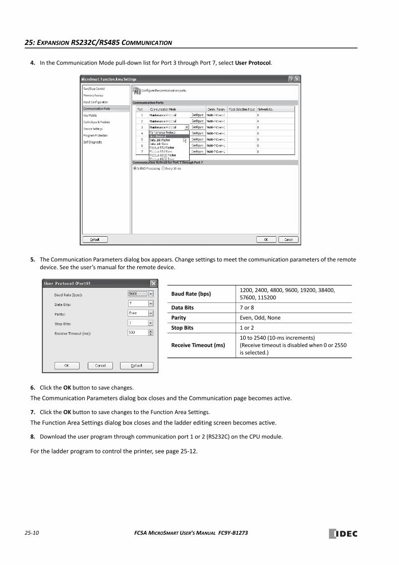
25: EXPANSION RS232C/RS485 COMMUNICATION
4. In the Communication Mode pull‐down list for Port 3 through Port 7, select User Protocol.
5. The Communication Parameters dialog box appears. Change settings to meet the communication parameters of the remote device. See the user’s manual for the remote device.
6. Click the OK button to save changes.
The Communication Parameters dialog box closes and the Communication page becomes active.
7. Click the OK button to save changes to the Function Area Settings.
The Function Area Settings dialog box closes and the ladder editing screen becomes active.
8. Download the user program through communication port 1 or 2 (RS232C) on the CPU module.
For the ladder program to control the printer, see page 25‐12.
Baud Rate (bps)1200, 2400, 4800, 9600, 19200, 38400, 57600, 115200
Data Bits 7 or 8
Parity Even, Odd, None
Stop Bits 1 or 2
Receive Timeout (ms)10 to 2540 (10‐ms increments)(Receive timeout is disabled when 0 or 2550 is selected.)
25‐10 FC5A MICROSMART USER’S MANUAL FC9Y‐B1273
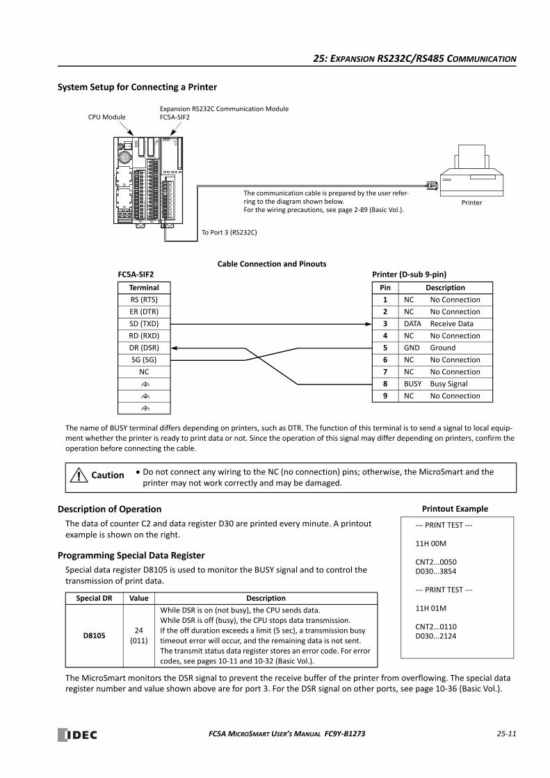
25: EXPANSION RS232C/RS485 COMMUNICATION
System Setup for Connecting a Printer
The name of BUSY terminal differs depending on printers, such as DTR. The function of this terminal is to send a signal to local equip‐ment whether the printer is ready to print data or not. Since the operation of this signal may differ depending on printers, confirm the operation before connecting the cable.
Description of Operation
The data of counter C2 and data register D30 are printed every minute. A printout example is shown on the right.
Programming Special Data Register
Special data register D8105 is used to monitor the BUSY signal and to control the transmission of print data.
The MicroSmart monitors the DSR signal to prevent the receive buffer of the printer from overflowing. The special data register number and value shown above are for port 3. For the DSR signal on other ports, see page 10‐36 (Basic Vol.).
Do not connect any wiring to the NC (no connection) pins; otherwise, the MicroSmart and the printer may not work correctly and may be damaged.
Special DR Value Description
D810524
(011)
While DSR is on (not busy), the CPU sends data.While DSR is off (busy), the CPU stops data transmission.If the off duration exceeds a limit (5 sec), a transmission busy timeout error will occur, and the remaining data is not sent. The transmit status data register stores an error code. For error codes, see pages 10‐11 and 10‐32 (Basic Vol.).
+ Ð24VDC
PWRSDRD
RS232C
RS
ER
SD
RD
DR
SG
NC
To Port 3 (RS232C)
CPU Module
The communication cable is prepared by the user refer‐ring to the diagram shown below. For the wiring precautions, see page 2‐89 (Basic Vol.).
Expansion RS232C Communication ModuleFC5A‐SIF2
Printer
Printer (D‐sub 9‐pin)
Pin Description
1 NC No Connection
2 NC No Connection
3 DATA Receive Data
4 NC No Connection
5 GND Ground
6 NC No Connection
7 NC No Connection
8 BUSY Busy Signal
9 NC No Connection
FC5A‐SIF2
Terminal
RS (RTS)
ER (DTR)
SD (TXD)
RD (RXD)
DR (DSR)
SG (SG)
NC
Cable Connection and Pinouts
Caution
‐‐‐ PRINT TEST ‐‐‐
11H 00M
CNT2...0050D030...3854
‐‐‐ PRINT TEST ‐‐‐
11H 01M
CNT2...0110D030...2124
Printout Example
FC5A MICROSMART USER’S MANUAL FC9Y‐B1273 25‐11
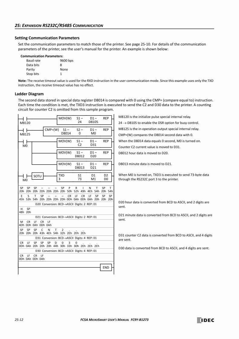
25: EXPANSION RS232C/RS485 COMMUNICATION
Setting Communication Parameters
Set the communication parameters to match those of the printer. See page 25‐10. For details of the communication parameters of the printer, see the user’s manual for the printer. An example is shown below:
Note: The receive timeout value is used for the RXD instruction in the user communication mode. Since this example uses only the TXD instruction, the receive timeout value has no effect.
Ladder Diagram
The second data stored in special data register D8014 is compared with 0 using the CMP= (compare equal to) instruction. Each time the condition is met, the TXD3 instruction is executed to send the C2 and D30 data to the printer. A counting circuit for counter C2 is omitted from this sample program.
Communication Parameters:Baud rate 9600 bpsData bits 8Parity NoneStop bits 1
S1 –24M8120
REPD1 –D8105
S2 –0
REPD1 –M0
M8120 is the initialize pulse special internal relay.
24 D8105 to enable the DSR option for busy control.
M8125 is the in‐operation output special internal relay.
CMP=(W) compares the D8014 second data with 0.
When the D8014 data equals 0 second, M0 is turned on.
Counter C2 current value is moved to D31.
D8012 hour data is moved to D20.
D8013 minute data is moved to D21.
When M0 is turned on, TXD3 is executed to send 73‐byte data through the RS232C port 3 to the printer.
D20 hour data is converted from BCD to ASCII, and 2 digits are sent.
D21 minute data is converted from BCD to ASCII, and 2 digits are sent.
D31 counter C2 data is converted from BCD to ASCII, and 4 digits are sent.
D30 data is converted from BCD to ASCII, and 4 digits are sent.
END
SOTU
SP20h
SP20h
SP20h
–2Dh
–2Dh
–2Dh
SP20h
P50h
R52h
I49h
N4Eh
T54h
SP20h
T54h
E45h
S53h
T54h
SP20h
–2Dh
–2Dh
–2Dh
CR0Dh
LF0Ah
CR0Dh
LF0Ah
SP20h
SP20h
SP20h
D20 Conversion: BCDASCII Digits: 2 REP: 01
H48h
SP20h
D21 Conversion: BCDASCII Digits: 2 REP: 01
M4Dh
CR0Dh
LF0Ah
CR0Dh
LF0Ah
SP20h
SP20h
SP20h
C43h
N4Eh
T54h
232h
.2Eh
.2Eh
.2Eh
D31 Conversion: BCDASCII Digits: 4 REP: 01
CR0Dh
LF0Ah
SP20h
SP20h
SP20h
D44h
030h
333h
030h
.2Eh
.2Eh
.2Eh
D30 Conversion: BCDASCII Digits: 4 REP: 01
CR0Dh
LF0Ah
CR0Dh
LF0Ah
S173
D2D0
D1M1
M0
M0
MOV(W)
TXD3
CMP=(W) S1 –D8014M8125
S1 –C2
REPD1 –D31
MOV(W)
S1 –D8012
REPD1 –D20
MOV(W)
S1 –D8013
REPD1 –D21
MOV(W)
25‐12 FC5A MICROSMART USER’S MANUAL FC9Y‐B1273
25: EXPANSION RS232C/RS485 COMMUNICATION
TroubleshootingThis section describes the procedures to determine the cause of trouble and actions to be taken when any trouble occurs while operating the expansion RS232C/RS485 communication module. When a problem occurred, check the points and take the actions described below. If the problem cannot be solved, call IDEC for assistance.
The PWR (power) LED does not go on.
The expansion RS232C/RS485 communication module cannot communicate with WindLDR.
The expansion RS232C/RS485 communication module cannot communicate with an operator interface.
Communication response is slow.
Check Action Page
Is power supplied to the CPU module? Supply power to the CPU module.Basic Vol.3‐18, 3‐19
Is the power voltage correct?Supply the rated power voltage.All‐in‐one type: 100‐240V AC or 24V DCSlim type: 24V DC
Basic Vol.3‐18, 3‐19
Check Action Page
Is the communication cable connected correctly? Connect the communication cable correctly.Basic Vol.2‐89, 25‐2
Is the PWR LED on the CPU module on? See “The PWR (power) LED does not go on.” 25‐13
Is the PWR LED on the FC5A‐SIF4 module flashing? Supply the rated voltage to the CPU module.Basic Vol.
3‐1
Are the communication settings for WindLDR and expan‐sion communication port the same?
Set the same communication parameters for WindLDR and expansion communication port.
25‐4
Is the CPU module system program version applicable to the expansion RS232C/RS485 communication module?
Upgrade the CPU module system program version to 110 or higher to use the FC5A‐SIF2 or to 220 or higher to use the FC5A‐SIF4.To download or upload a user program, upgrade the system program version to 220 or higher.
Basic Vol.A‐9
Check Action Page
Is the communication cable connected correctly? Connect the communication cable correctly.Basic Vol.2‐89, 25‐6
Is the PWR LED on the CPU module on? See “The PWR (power) LED does not go on.” 25‐13
Is the PWR LED on the FC5A‐SIF4 module flashing? Supply the rated voltage to the CPU module.Basic Vol.
3‐1
Are the communication settings for the operator interface and expansion communication port the same?
Set the same communication parameters for the operator interface and expansion communication port.
25‐7
Is the CPU module system program version applicable to the expansion RS232C/RS485 communication module?
Upgrade the CPU module system program version to 110 or higher to use the FC5A‐SIF2 or to 220 or higher to use the FC5A‐SIF4.
Basic Vol.A‐9
Check Action Page
Is the communication baud rate set to a proper value?Set the communication baud rate to a required value.
25‐3, 25‐7, 25‐9
Is the COMRF instruction used in the user program? Use the COMRF instruction in the user program. 11‐13
FC5A MICROSMART USER’S MANUAL FC9Y‐B1273 25‐13
25: EXPANSION RS232C/RS485 COMMUNICATION
Data is not transmitted at all in the user communication.
Data is not transmitted correctly in the user communication.
Data is not received at all in the user communication.
Check Action Page
Is the communication cable connected correctly? Make sure of correct wiring.Basic Vol.2‐89, 25‐11
Are the communication settings for the remote terminal and expansion RS232C/RS485 communication port the same?
Set the same communication parameters for expan‐sion communication port as the remote terminal.
25‐10
Is the CPU module system program version applicable to the expansion RS232C/RS485 communication module?
Upgrade the CPU module system program version to 110 or higher to use the FC5A‐SIF2 or to 220 or higher to use the FC5A‐SIF4.
Basic Vol.A‐9
Is the correct port number designated in the TXD instruc‐tion?
Designate a correct port number in the TXD instruc‐tion.
Basic Vol.10‐7
Is the start input for the TXD instruction on? Turn on the start input for the TXD instruction. 25‐12
Is the PWR LED on the CPU module on? See “The PWR (power) LED does not go on.” 25‐13
Is the PWR LED on the FC5A‐SIF4 module flashing? Supply the rated voltage to the CPU module.Basic Vol.
3‐1
Check Action Page
Are the communication settings for the external device and expansion communication port the same?
Set the same communication parameters for expan‐sion communication port as the external device.
25‐10
Is the same data register designated as destination device D2 (transmit status) repeatedly?
Change the duplicate device to another data regis‐ter.
Basic Vol.10‐6
Are inputs to more than 5 TXD instructions on simultane‐ously?
Correct the program to make sure that inputs to more than 5 TXD instructions do not go on simulta‐neously.
Basic Vol.10‐6
Is duration of the busy signal at the remote terminal less than 5 sec?
Make sure that the busy signal at the remote termi‐nal does not exceed 5 sec.
Basic Vol.10‐38
Did you make sure of source 1 device of the TXD instruc‐tion?
Make sure that the transmit data designated as source 1 device is correct.
Basic Vol.10‐7
Is the PWR LED on the FC5A‐SIF4 module flashing? Supply the rated voltage to the CPU module.Basic Vol.
3‐1
Check Action Page
Is the communication cable connected correctly? Make sure of correct wiring.Basic Vol.2‐89, 25‐11
Are the communication settings for the remote terminal and expansion RS232C/RS485 communication port the same?
Set the same communication parameters for expan‐sion RS232C communication port as the remote ter‐minal.
25‐10
Is the CPU module system program version applicable to the expansion RS232C/RS485 communication module?
Upgrade the CPU module system program version to 110 or higher to use the FC5A‐SIF2 or to 220 or higher to use the FC5A‐SIF4.
Basic Vol.A‐9
Is the correct port number designated in the RXD instruc‐tion?
Designate a correct port number in the RXD instruc‐tion.
Basic Vol.10‐6
Is the start input for the RXD instruction on? Turn on the start input for the RXD instruction.Basic Vol.10‐39
Is the PWR LED on the CPU module on? See “The PWR (power) LED does not go on.” 25‐13
Is the PWR LED on the FC5A‐SIF4 module flashing? Supply the rated voltage to the CPU module.Basic Vol.
3‐1
25‐14 FC5A MICROSMART USER’S MANUAL FC9Y‐B1273
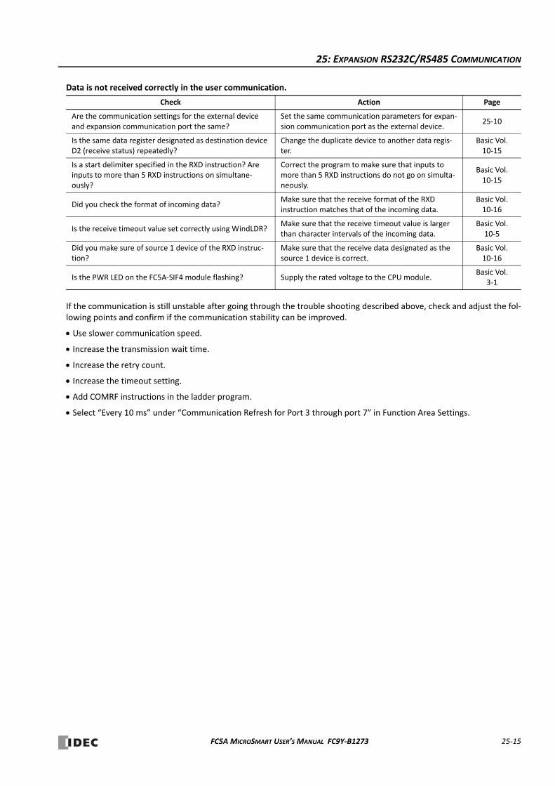
25: EXPANSION RS232C/RS485 COMMUNICATION
Data is not received correctly in the user communication.
If the communication is still unstable after going through the trouble shooting described above, check and adjust the fol‐lowing points and confirm if the communication stability can be improved.
Use slower communication speed.
Increase the transmission wait time.
Increase the retry count.
Increase the timeout setting.
Add COMRF instructions in the ladder program.
Select “Every 10 ms” under “Communication Refresh for Port 3 through port 7” in Function Area Settings.
Check Action Page
Are the communication settings for the external device and expansion communication port the same?
Set the same communication parameters for expan‐sion communication port as the external device.
25‐10
Is the same data register designated as destination device D2 (receive status) repeatedly?
Change the duplicate device to another data regis‐ter.
Basic Vol.10‐15
Is a start delimiter specified in the RXD instruction? Are inputs to more than 5 RXD instructions on simultane‐ously?
Correct the program to make sure that inputs to more than 5 RXD instructions do not go on simulta‐neously.
Basic Vol.10‐15
Did you check the format of incoming data?Make sure that the receive format of the RXD instruction matches that of the incoming data.
Basic Vol.10‐16
Is the receive timeout value set correctly using WindLDR?Make sure that the receive timeout value is larger than character intervals of the incoming data.
Basic Vol.10‐5
Did you make sure of source 1 device of the RXD instruc‐tion?
Make sure that the receive data designated as the source 1 device is correct.
Basic Vol.10‐16
Is the PWR LED on the FC5A‐SIF4 module flashing? Supply the rated voltage to the CPU module.Basic Vol.
3‐1
FC5A MICROSMART USER’S MANUAL FC9Y‐B1273 25‐15

25: EXPANSION RS232C/RS485 COMMUNICATION
25‐16 FC5A MICROSMART USER’S MANUAL FC9Y‐B1273
INDEX
# 1:N computer link 21‐1
100‐msdual timer 15‐1
10‐msdual timer 15‐1
1‐ms dual timer 15‐1
1‐secdual timer 15‐1
A A/B slaves 24‐4
ACOS 17‐7
active slaves (LAS) 24‐26
adapterRS485 communication 21‐1
ADD 5‐1
addition 5‐1
addressLEDs 24‐16
and I/O LEDs 24‐17
addressing tool 24‐4
adjustingclockcartridge accuracy 9‐8
using a user program 9‐7
scan time 10‐4
advanced instruction 2‐1
ACOS 17‐7
ADD 5‐1
ALT 8‐18
ANDW 6‐1
applicable CPU modules 2‐4
ASIN 17‐6
ATAN 17‐8
ATOB 8‐12
ATOH 8‐7
AVRG 12‐7
BCDLS 7‐5
BCNT 8‐17
BMOV 3‐9
BTOA 8‐9
BTOH 8‐3
CMP< 4‐1
CMP<= 4‐1
CMP<> 4‐1
CMP= 4‐1
CMP> 4‐1
CMP>= 4‐2
COMRF 11‐13
COS 17‐4
CVDT 8‐19
CVXTY 12‐2
CVYTX 12‐3
data types 2‐8
DEC 5‐13
DECO 8‐16
DEG 17‐2
DGRD 10‐3
DI 11‐7
FC5A MICROSMART USER
DISP 10‐1
DIV 5‐1
DJNZ 11‐5
DTCB 8‐22
DTDV 8‐21
DTIM 15‐1
DTMH 15‐1
DTML 15‐1
DTMS 15‐1
EI 11‐7
ENCO 8‐15
EXP 18‐3
FIEX 19‐3
FIFOF 19‐1
FOEX 19‐3
FRQRF 11‐12
HOUR 20‐11
HSCRF 11‐11
HTOA 8‐5
HTOB 8‐1
HTOS 20‐9
IBMV 3‐10
IBMVN 3‐12
ICMP>= 4‐6
IMOV 3‐6
IMOVN 3‐8
INC 5‐13
input condition 2‐7
IOREF 11‐9
LABEL 11‐1
LC< 4‐8
LC<= 4‐8
LC<> 4‐8
LC= 4‐8
LC> 4‐8
LC>= 4‐8
LCAL 11‐3
list 2‐1
LJMP 11‐1
LOG10 18‐2
LOGE 18‐1
LRET 11‐3
MOV 3‐1
MOVN 3‐5
MUL 5‐1
NDSRC 19‐5
NOP 2‐10
NRS 3‐14
NSET 3‐13
ORW 6‐1
PID 14‐1
POW 18‐4
PULS1 13‐2
PULS2 13‐2
PULS3 13‐2
PWM1 13‐8
PWM2 13‐8
PWM3 13‐8
’S MANUAL FC9Y‐B1273 i
INDEX
RAD 17‐1
RAMP1 13‐14
RAMP2 13‐14
RNDM 5‐19
ROOT 5‐15
ROTL 7‐8
ROTR 7‐10
RUNA READ 16‐2
RUNA WRITE 16‐3
SFTL 7‐1
SFTR 7‐3
SIN 17‐3
STOH 20‐10
STPA READ 16‐4
STPA WRITE 16‐5
structure 2‐7
SUB 5‐1
SUM 5‐16
SWAP 8‐23
TADD 20‐1
TAN 17‐5
TCCST 3‐16
TSUB 20‐5
TTIM 15‐3
WKTBL 9‐2
WKTIM 9‐1
WSFT 7‐7
XCHG 3‐15
XORW 6‐1
XYFS 12‐1
ZRN1 13‐26
ZRN2 13‐26
ZRN3 13‐26
allocating communication port number 25‐1
ALT 8‐18
alternate output 8‐18
analogI/Odata 24‐22
inputdata 24‐22
outputdata 24‐23
slave profile 24‐22
AND word 6‐1
ANDW 6‐1
answer mode 22‐2, 22‐6APF/not APO 24‐25
applicablesensors and actuators 24‐1
arccosine 17‐7
sine 17‐6
tangent 17‐8
ASCIIto BCD 8‐12
to hex 8‐7
ASI commands 24‐30
ASIN 17‐6
AS‐Interface 24‐1
buscycle time 24‐5
ii FC5A MicroSmart User’s
topology and maximum length 24‐5
cable 24‐3
wiring 24‐6
devices 24‐18
objects 24‐19
power supply 24‐3
standard cable 24‐3
system setup 24‐6
assigning a slave address 24‐9
AT 14‐12
commandexecution 22‐2
result code 22‐3
string 22‐3
general command mode 22‐2, 22‐5ATAN 17‐8
ATOB 8‐12
ATOH 8‐7
ATZ 22‐2, 22‐4, 22‐6auto tuning 14‐12
Auto_Address_Assign 24‐25
Auto_Address_Available 24‐25
average 12‐7
AVRG 12‐7
B backupduration clock cartridge 9‐8
basicinstructions 1‐1
BCDleft shift 7‐5
to ASCII 8‐9
to hex 8‐3
BCDLS 7‐5
BCNT 8‐17
binary arithmetic instructions 5‐1
bit count 8‐17
block move 3‐9
BMOV 3‐9
BMOV/WSFT executing flag M8024 3‐9, 7‐7Boolean computation instructions 6‐1
BTOA 8‐9
BTOH 8‐3
busysignal 25‐11
C cable 24‐3, 25‐2, 25‐3, 25‐6, 25‐7, 25‐11AS‐Interface 24‐3
computer link 4C 24‐6, 25‐2, 25‐6expansion communicationRS232C 25‐2
RS485 25‐3
modem 1C 22‐1
RS232C 21‐1
calendar/clocksetting usinga user program 9‐6
WindLDR 9‐6
carryand borrow 5‐17
or borrow signals 5‐2
CDI 24‐27
changing
Manual FC9Y‐B1273
INDEX
ID1 code of slave 0 24‐29
clockadjusting using a user program 9‐7
cartridgeadjusting accuracy 9‐8
backup duration 9‐8
enable adjustment 9‐8
instructions 20‐1
CMP< 4‐1
CMP<= 4‐1
CMP<> 4‐1
CMP= 4‐1
CMP> 4‐1
CMP>= 4‐2
common logarithm 18‐2
communicationblock mounting position 24‐40
parameters 21‐2, 22‐10, 25‐4, 25‐10, 25‐12portnumber 25‐1
refresh 11‐13
settings 21‐3, 23‐4compareequal to 4‐1
greater than 4‐1
or equal to 4‐2
less than 4‐1
or equal to 4‐1
unequal to 4‐1
comparisonresultM8150, M8151, M8152 4‐2, 4‐6
computer linkcable 4C 24‐6, 25‐2, 25‐6communication 21‐1, 25‐2
COMRF 11‐13
execution time 11‐13
Config_OK 24‐24
Configuration 24‐25
configuration 24‐36
data image (CDI) 24‐27
mode 24‐15
configure AS‐Interface master 24‐34
configuring a slave 24‐10
Connected Mode 24‐25
connected mode 24‐15
connector pinout 22‐1
controlregister 13‐2, 13‐9, 13‐15, 13‐27, 14‐3relay 14‐14
conversion 10‐1, 10‐3linear 12‐5
convertdata type 8‐19
X to Y 12‐2
Y to X 12‐3
coordinate conversion instructions 12‐1
COS 17‐4
cosine 17‐4
CVDT 8‐19
CVXTY 12‐2
CVYTX 12‐3
FC5A MICROSMART USER
cycle time 24‐5
D datacombine 8‐22
comparison instructions 4‐1
conversionerror 12‐3, 12‐4instructions 8‐1
divide 8‐21
phase 10‐1
swap 8‐23
type 2‐7
types for advanced instructions 2‐8
data registerdouble‐worddata move 3‐2
devices 2‐10
Data_Exchange_Active 24‐25
DEC 5‐13
deceleration input 13‐28
decimal values and hexadecimal storage 2‐8
DECO 8‐16
decode 8‐16
decrement 5‐13
jump non‐zero 11‐5
DEG 17‐2
degree 17‐2
destination device 2‐7
detected slaves (LDS) 24‐26
deviceareas discontinuity 2‐10
AS‐Interface 24‐18
DGRD 10‐3
DI 11‐7
dialing 22‐2
telephone number 22‐4
digitalI/O data allocation 24‐39, 24‐40input data image 24‐20
output data image 24‐21
read 10‐3
switch data reading time 10‐3
directcontrol action 14‐14
disableinterrupt 11‐7
disconnectline 22‐2
mode 22‐2, 22‐5discontinuity of device areas 2‐10
DISP 10‐1
display 10‐1
processing time 10‐1
DIV 5‐1
division 5‐1
DJNZ 11‐5
double‐worddata move in data registers 3‐2
devices in data registers 2‐10
DTCB 8‐22
DTDV 8‐21
DTIM 15‐1
DTMH 15‐1
’S MANUAL FC9Y‐B1273 iii
INDEX
DTML 15‐1
DTMS 15‐1
dual/teaching timer instructions 15‐1
E EI 11‐7
enableclock cartridge adjustment 9‐8
interrupt 11‐7
ENCO 8‐15
encode 8‐15
errorcode 24‐35, 24‐36, 24‐37, 24‐38messages 24‐38
exchange 3‐15
exclusive OR word 6‐1
executiontime COMRF 11‐13
EXP 18‐3
expansioncapability 24‐4
RS232C/RS485 communication 25‐1
exponent 18‐3
F FIEX 19‐3
FIFO format 19‐1
FIFOF 19‐1
file data processing instructions 19‐1
first‐in execute 19‐3
first‐out execute 19‐3
flat cable 24‐3
FOEX 19‐3
format number 12‐1, 12‐2, 12‐3frequency measurementrefresh 11‐12
FRQRF 11‐12
functionarea settings 24‐8
H hex toASCII 8‐5
BCD 8‐1
hexadecimal storage decimal values 2‐8
high‐speed counterrefresh 11‐11
HMS to sec 20‐9
HOUR 20‐11
hour meter 20‐11
HSCRF 11‐11
HTOA 8‐5
HTOB 8‐1
HTOS 20‐9
HW series digital I/O data allocation 24‐40
I I/Ocode 24‐4
data 24‐20
refresh 11‐9
IBMV 3‐10
IBMVN 3‐12
ICMP>= 4‐6
ID code 24‐4
ID1 code 24‐4
of slave 0 24‐29
iv FC5A MicroSmart User’s
ID2 code 24‐4
identification 24‐4
IDI 24‐20
IMOV 3‐6
IMOVN 3‐8
INC 5‐13
increment 5‐13
indirectbit move 3‐10
bit move not 3‐12
move 3‐6
move not 3‐8
initialization string 22‐2, 22‐3, 22‐6commands 22‐8
inputcondition for advanced instructions 2‐7
data 24‐39, 24‐40LEDs 24‐16
points 10‐3
instructionsbinary arithmetic 5‐1
Boolean computation 6‐1
clock 20‐1
coordinate conversion 12‐1
data comparison 4‐1
data conversion 8‐1
dual/teaching timer 15‐1
file data processing 19‐1
intelligent module access 16‐1
interface 10‐1
logarithm/power 18‐1
move 3‐1
PID 14‐1
program branching 11‐1
pulse 13‐1
shift/rotate 7‐1
trigonometric function 17‐1
week programmer 9‐1
intelligent module accessinstructions 16‐1
status code 16‐6
interface instructions 10‐1
internalrelayfor SwitchNet slaves 24‐41
interval compare greater than or equal to 4‐6
IOREF 11‐9
L L6 series digital I/O data allocation 24‐39
LABEL 11‐1
label 11‐1
call 11‐3
jump 11‐1
return 11‐3
LAPP?s cables 24‐3
LAS 24‐26
latch phase 10‐1
LC< 4‐8
LC<= 4‐8
LC<> 4‐8
LC= 4‐8
LC> 4‐8
LC>= 4‐8
Manual FC9Y‐B1273
INDEX
LCAL 11‐3
LDS 24‐26
LDS.0 24‐24
LED indicators 24‐14, 24‐16lineconnection 22‐2
linear conversion 12‐5
listadvanced instruction 2‐1
basic instruction 1‐1
of active slaves (LAS) 24‐26
of detected slaves (LDS) 24‐26
of peripheral fault slaves (LPF) 24‐26
of projected slaves (LPS) 24‐27
upgraded and new functions 1‐2
LJMP 11‐1
load compareequal to 4‐8
greater than 4‐8
or equal to 4‐8
less than 4‐8
or equal to 4‐8
unequal to 4‐8
local mode 24‐15
LOG10 18‐2
logarithm/power instructions 18‐1
LOGE 18‐1
long press 24‐14
LPF 24‐26
LPS 24‐27
LRET 11‐3
M maintenanceprotocol 21‐2, 25‐4
manipulated variable 14‐16
maximumAS‐Interface bus cycle time 24‐5
Modbus TCPcommunication 23‐1
format 23‐9
mastercommunication 23‐2
request table 23‐3
slave communication 23‐5
mode 9‐1
modemcable 1C 22‐1
mode 22‐1
status 22‐3
status data register 22‐7
protocol 22‐10
moduleRS485 communication 21‐1
monitorAS‐Interface slave 24‐37
monitoringdigital I/O and changing output status 24‐12
PLC status 21‐3
mountingposition communication block 24‐40
MOV 3‐1
move 3‐1
instructions 3‐1
FC5A MICROSMART USER
not 3‐5
MOVN 3‐5
MUL 5‐1
multiplication 5‐1
N N datarepeat set 3‐14
search 19‐5
set 3‐13
natural logarithm 18‐1
NDSRC 19‐5
network number 21‐3
no operation 2‐10
NOP 2‐10
normalprotecteddata exchange off 24‐15
mode 24‐15
offline 24‐15
Normal_Operation_Active 24‐25
NRS 3‐14
NSET 3‐13
O ODI 24‐21
Off‐line 24‐25
Offline_Ready 24‐25
onlinemode protocol selection 22‐3
opcode 2‐7
operatingproceduremodem mode 22‐11
operationbasics 24‐6
mode 24‐15
operational state 22‐2
operator interface communication 25‐6
OR word 6‐1
originate mode 22‐2, 22‐3ORW 6‐1
outputdata 24‐39, 24‐40LEDs 24‐16
points 10‐1, 10‐3overlapping coordinates 12‐6
P parameter 24‐4
image (PI) 24‐28
PCD 24‐28
peripheral fault slaves (LPF) 24‐26
Periphery_OK 24‐25
permanentconfiguration data (PCD) 24‐28
parameter (PP) 24‐29
PI 24‐28
PIDcontrol 14‐1
instruction 14‐1
notes for using 14‐17
pinout 22‐1
PLC statusmonitoring 21‐3
POW 18‐4
’S MANUAL FC9Y‐B1273 v
INDEX
power 18‐4
supply 24‐7
AS‐Interface 24‐3
wiring 24‐7
PP 24‐29
preparations for using modem 22‐9
printer 25‐11
process variable before conversion 14‐16
processing time 24‐18, 24‐30profile 24‐27
analog slave 24‐22
program branchinginstructions 11‐1
using with SOTU/SOTD instructions 11‐2
using with timer instruction 11‐2
programmingclock cartridge accuracy using WindLDR 9‐8
computer link using WindLDR 21‐2
data registers and internal relays 22‐9
DI or EI using WindLDR 11‐7
Modbus TCPmaster using WindLDR 23‐3
slave using WindLDR 23‐7
modem mode using WindLDR 22‐10
special data register 25‐11
projected slaves (LPS) 24‐27
protected mode 24‐15
PULS1 13‐2
PULS2 13‐2
PULS3 13‐2
pulseinstructions 13‐1
output 13‐2
width modulation 13‐8
pushbutton operation 24‐14
pushbuttons and LED indicators 24‐14
PWM1 13‐8
PWM2 13‐8
PWM3 13‐8
Q quantities of slaves and I/O points 24‐5
R RAD 17‐1
radian 17‐1
ramp control 13‐14
RAMP1 13‐14
RAMP2 13‐14
random 5‐19
readingtime digital switch data 10‐3
receiveslave data 24‐39, 24‐40timeout 21‐2, 25‐3, 25‐4, 25‐7, 25‐9, 25‐10
repeatcycles 2‐7
designation 2‐7
operationADD and SUB instructions 5‐6
ANDW, ORW, and XORW instructions 6‐3
data comparison instructions 4‐4
DIV instruction 5‐10
indirect bit move instruction 3‐11
move instructions 3‐3
vi FC5A MicroSmart User’s
MUL instruction 5‐8
requestand result codes 24‐31
table 23‐4
resettingmodem 22‐4, 22‐6
retrycycles 22‐3
interval 22‐3
reversecontrol action 14‐14
revision history 1‐3
RNDM 5‐19
ROOT 5‐15
rotateleft 7‐8
right 7‐10
ROTL 7‐8
ROTR 7‐10
RS232Ccable 21‐1
communicationadapter 22‐1
expansion communication 25‐1
portcommunication protocol 22‐5
RS232C/RS485 converter 21‐1
RS485communicationadapter 21‐1
module 21‐1
expansion communication 25‐1
run accessread 16‐2
write 16‐3
RUNA READ 16‐2
RUNA WRITE 16‐3
S sample programchange slave PI 24‐31
modem answer mode 22‐13
modem originate mode 22‐12
scan timeadjusting 10‐4
sec to HMS 20‐10
selecting the PLC type 24‐8
send slave data 24‐39, 24‐40set point 14‐16
settingcalendar/clockusing a user program 9‐6
using WindLDR 9‐6
SFTL 7‐1
SFTR 7‐3
shiftleft 7‐1
right 7‐3
shift/rotate instructions 7‐1
short press 24‐14
SIN 17‐3
sine 17‐3
slaveaddresses 24‐4
Manual FC9Y‐B1273
INDEX
expansion capability 24‐4
identification 24‐4
information 24‐27
list information 24‐26
profile 24‐27
analog 24‐22
receive data 24‐39, 24‐40send data 24‐39, 24‐40
SOTU/SOTD instructions using with program branching 11‐2
sourceand destination devices 2‐7
device 2‐7
special data registerfor calendar/clock data 9‐6
for modem mode 22‐3
for pulse outputs 13‐5, 13‐19special internal relayfor calendar/clock data 9‐7
for interrupt status 11‐7
for modem mode 22‐2
specificationsModbus TCPmaster communication 23‐2
slave communication 23‐6
standard slaves 24‐4
startand result internal relays 22‐2
statuscodeintelligent module access 16‐6
data register modem mode 22‐7
information 24‐24
internal relays 24‐24
internal relays 22‐2
LEDs 24‐16, 24‐17relay 13‐4, 13‐10, 13‐19, 13‐29
step response method 14‐12
STOH 20‐10
stopaccessread 16‐4
write 16‐5
STPA READ 16‐4
STPA WRITE 16‐5
structure of an advanced instruction 2‐7
SUB 5‐1
subroutine 11‐4
subtraction 5‐1
SUM 5‐16
sum 5‐16
SWAP 8‐23
SwitchNetdata I/O port 24‐39
slaves internal relays 24‐41
systemrequirements 24‐2
setup 24‐6
modem mode 22‐1
T TADD 20‐1
TAN 17‐5
tangent 17‐5
FC5A MICROSMART USER
TCCST 3‐16
teaching timer 15‐3
telephone number 22‐3, 22‐4timeaddition 20‐1
subtraction 20‐5
timerinstruction using with program branching 11‐2
or counteras destination device 2‐7
as source device 2‐7
timer/countercurrent valuestore 3‐16
timing chartdisable pulse counting 13‐6, 13‐12enable pulse counting 13‐5, 13‐11reversible controldisabled 13‐20
with dual pulse output 13‐22
with single pulse output 13‐21
zero‐return operation 13‐30
topology 24‐5
transition of AS‐Interface master module modes 24‐14
trigonometric function instructions 17‐1
troubles at system start‐up 24‐13
troubleshooting 25‐13
modem communication 22‐14
TSUB 20‐5
TTIM 15‐3
U usercommunication 25‐9
programadjusting clock 9‐7
setting calendar/clock 9‐6
protocol 25‐10
using WindLDR 24‐34
V very low safety voltage 24‐3, 24‐7VLSV 24‐3, 24‐7
W weekprogrammer instructions 9‐1
table 9‐2
timer 9‐1
WindLDRprogrammingclock cartridge accuracy 9‐8
computer link 21‐2
DI or EI 11‐7
Modbus TCPmaster 23‐3
slave 23‐7
modem mode 22‐10
setting calendar/clock 9‐6
WKTBL 9‐2
WKTIM 9‐1
word shift 7‐7
WSFT 7‐7
X XCHG 3‐15
XORW 6‐1
’S MANUAL FC9Y‐B1273 vii

INDEX
XY format set 12‐1
XYFS 12‐1
Z zero return 13‐26
ZRN1 13‐26
ZRN2 13‐26
ZRN3 13‐26
viii FC5A MicroSmart User’s
Manual FC9Y‐B1273
NOTE
FC5A MICROSMART USER’S MANUAL FC9Y‐B1273 1

NOTE
2 FC5A MICROSMART USER’S MANUAL FC9Y‐B1273

© 2009-2014 IDEC Corporation. All rights reserved.http://www.idec.com Manual No. FC9Y-B1273B-1273(2)
UNITED STATESIDEC CORPORATION1175 Elko Drive, Sunnyvale, CA 94089-2209, USATel: +1-408-747-0550Toll Free: (800) 262-IDECFax: +1-408-744-9055Toll Free Fax: (800) 635-6246E-mail: [email protected]
CANADAIDEC CANADA LIMITED3155 Pepper Mill Court, Unit 4,Mississauga, Ontario, L5L 4X7, CanadaTel: +1-905-890-8561Toll Free: (888) 317-4332Fax: +1-905-890-8562E-mail: [email protected]
AUSTRALIAIDEC AUSTRALIA PTY. LTD.17/104 Ferntree Gully Road, Oakleigh, Victoria 3166, AustraliaTel: +61-3-8523-5900Toll Free: 1800-68-4332Fax: +61-3-8523-5999E-mail: [email protected]
UNITED KINGDOMIDEC ELECTRONICS LIMITEDUnit 2, Beechwood, Chineham Business Park, Basingstoke, Hampshire RG24 8WA, UKTel: +44-1256-321000Fax: +44-1256-327755E-mail: [email protected]
GERMANYIDEC ELEKTROTECHNIK GmbHWendenstrasse 331, 20537 Hamburg, GermanyTel: +49-40-25 30 54 - 0Fax: +49-40-25 30 54-24E-mail: [email protected]
JAPANIDEC CORPORATION6-64, Nishi-Miyahara 2-Chome, Yodogawa-ku, Osaka 532-0004, JapanTel: +81-6-6398-2527Fax: +81-6-6398-2547E-mail: [email protected]
CHINAIDEC (SHANGHAI) CORPORATIONRoom 701-702 Chong Hing Finance Center, No.288 Nanjing Road West, Shanghai 200003, P.R.C.Tel: +86-21-6135-1515Fax: +86-21-6135-6225E-mail: [email protected]
IDEC (BEIJING) CORPORATIONRoom 211B, Tower B, The Grand Pacific Building, 8A Guanghua Road, Chaoyang District, Beijing 100026, PRCTEL: +86-10-6581-6131FAX: +86-10-6581-5119
IDEC (SHENZHEN) CORPORATIONUnit AB-3B2, Tian Xiang Building, Tian’an Cyber Park,Fu Tian District, Shenzhen, Guang Dong 518040, PRCTel: +86-755-8356-2977Fax: +86-755-8356-2944
HONG KONGIDEC IZUMI (H.K.) CO., LTD.Unit G & H, 26/F., MG Tower, No. 133 Hoi Bun Road, Kwun Tong, Kowloon, Hong KongTel: +852-2803-8989Fax: +852-2565-0171E-mail: [email protected]
TAIWANIDEC TAIWAN CORPORATION8F-1, No.79, Hsin Tai Wu Road, Sec.1, Hsi-Chih District, 22101 New Taipei City, TaiwanTel: +886-2-2698-3929Fax: +886-2-2698-3931E-mail: [email protected]
SINGAPOREIDEC IZUMI ASIA PTE. LTD.No. 31, Tannery Lane #05-01HB Centre 2, Singapore 347788Tel: +65-6746-1155Fax: +65-6844-5995E-mail: [email protected]
IDEC ASIA (THAILAND) CO.,LTD.20th Fl., Sorachai Bldg., No.23/78, Soi Sukhumvit 63, Sukhumvit Rd., Klongton-Nua, Wattana, Bangkok 10110Tel: +66-2-392-9765Fax: +66-2-392-9768E-mail: [email protected]
THAILAND