Embed Size (px)
Citation preview
Sample Linear fit equation VFB vs.RHE
(x-Intercept)
Dopant
concentration
(cm-1
)
Space charge
region width at
0V (vs. RHE)
ZB GaP Planar y = -2.34E+15x + 2.48E+15 1.06E+00 6.81E+18 14nm
WZ GaP Nanowires y= -1.09E+16x + 1.16E+16 1.06E+00 1.46E+18 30nm
Supplementary Figure 1. Mott-Schottky plots. Impedance measurements were performed in
the dark, in aqueous solution pH0 with HClO4 as supporting electrolyte. Mott-Schottky plots for
(a) ZB GaP planar and (b) WZ GaP nanowire samples were calculated from the Mott-Schottky
equation, which can be written as;
)(21
0
2 q
kTVV
NqCFB
SC
(1)
where CSC is the capacitance of the space charge region, q is the elementary charge, Ɛ0 is the
permittivity of free space, Ɛ is the dielectric constant of ZB GaP, N is the dopant concentration,
V is the applied potential, VFB is the flat band potential and approximate valence band position
(vs. RHE) for a p-type semiconductor, k is the Boltzmann constant and T is the temperature in
Kelvin. The data from the Mott-Schottky equation allows that calculation of the space charge
width, which can be written as;
2
1
2 2
kT
VVqW FB (2)
where W is the space charge region width. The table shows; the flat band potential (VFB), the
dopant concentration, and the width of the space charge region at 0V, for the ZB planar and WZ
nanowire GaP samples used.
-0.4 -0.2 0.0 0.2 0.4
8.0E15
1.2E16
1.6E16
C-2 (
cm
4 F
-2)
V (vs. RHE)
-0.2 -0.1 0.0 0.1 0.2 0.3 0.4 0.5
1.6E15
2.0E15
2.4E15
2.8E15
C-2 (
cm
4 F
-2)
V (vs. RHE)
a b
Supplementary Figure 2. The effect of nanowire length on photoelectrochemical
performance. a) SEM images of Zinc-doped WZ GaP nanowires grown for (i) 6min, (ii) 14min,
and (iii) 22min with lengths of 0.73µm, 1.65µm and 2.16µm respectively. Scale bar 200nm for
all images. b) Linear sweep voltammograms of NW samples with NW lengths of 0.73µm (black/
top), 2.02µm (blue/ middle) and 3.5µm (red/ bottom), performed under chopped 100mW/cm2
AM1.5 illumination, in aqueous solution pH0 with HClO4 as supporting electrolyte. c) Plots of
resistance (black, left y-axis) and ISC (red, right y-axis) against nanowire length. The error bars
were calculated as two standard deviations away from the average value taken from 3 or more
experiments carried out on separate samples with the same specifications
-1.4
-0.7
0.0
-0.2 0.0 0.2 0.4 0.6 0.8
-1.4
-0.7
0.0
-0.2 0.0 0.2 0.4 0.6 0.8
-1.4
-0.7
0.0
I (m
A/c
m2)
0.73µm
I (m
A/c
m2)
2.02µm
I (m
A/c
m2)
V (vs NHE)
3.5µm
0 1 2 3 4 5 6
20
40
60
80
100
120
Resi
stan
ce (
)
Resistance
ISC
Length (µm)
0.0
0.2
0.4
0.6
0.8
1.0
1.2
1.4
1.6 I
SC (
mA
/cm
2)
a (i) (ii) (iii)
b
c
0.5 1.0 1.5 2.0
18
21
24
27
Absorb
ed p
ow
er
(mW
/cm
2)
Length (m)
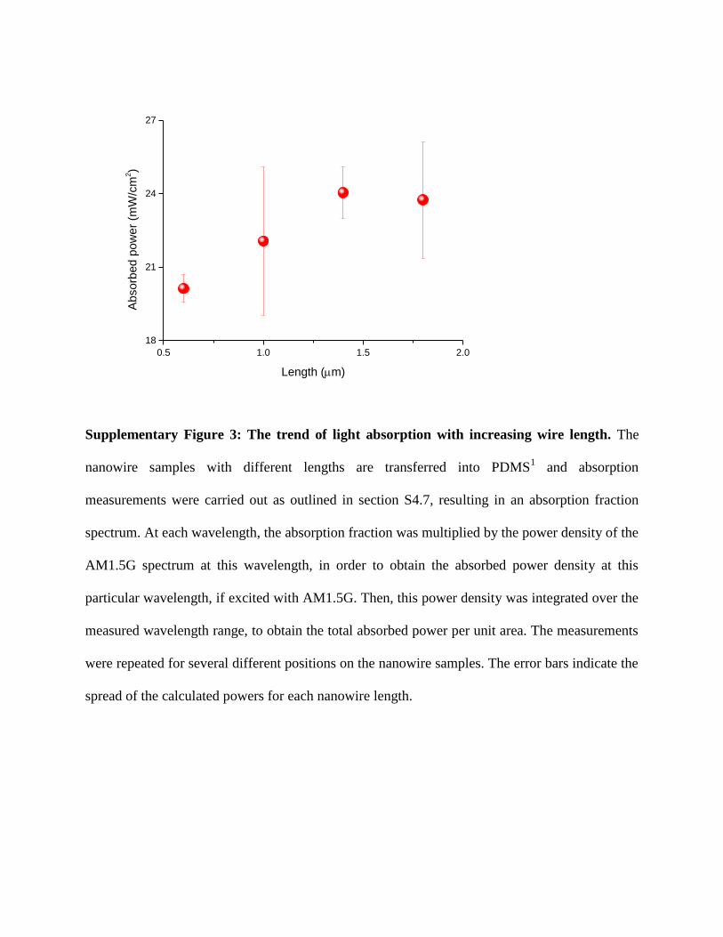
Supplementary Figure 3: The trend of light absorption with increasing wire length. The
nanowire samples with different lengths are transferred into PDMS1 and absorption
measurements were carried out as outlined in section S4.7, resulting in an absorption fraction
spectrum. At each wavelength, the absorption fraction was multiplied by the power density of the
AM1.5G spectrum at this wavelength, in order to obtain the absorbed power density at this
particular wavelength, if excited with AM1.5G. Then, this power density was integrated over the
measured wavelength range, to obtain the total absorbed power per unit area. The measurements
were repeated for several different positions on the nanowire samples. The error bars indicate the
spread of the calculated powers for each nanowire length.
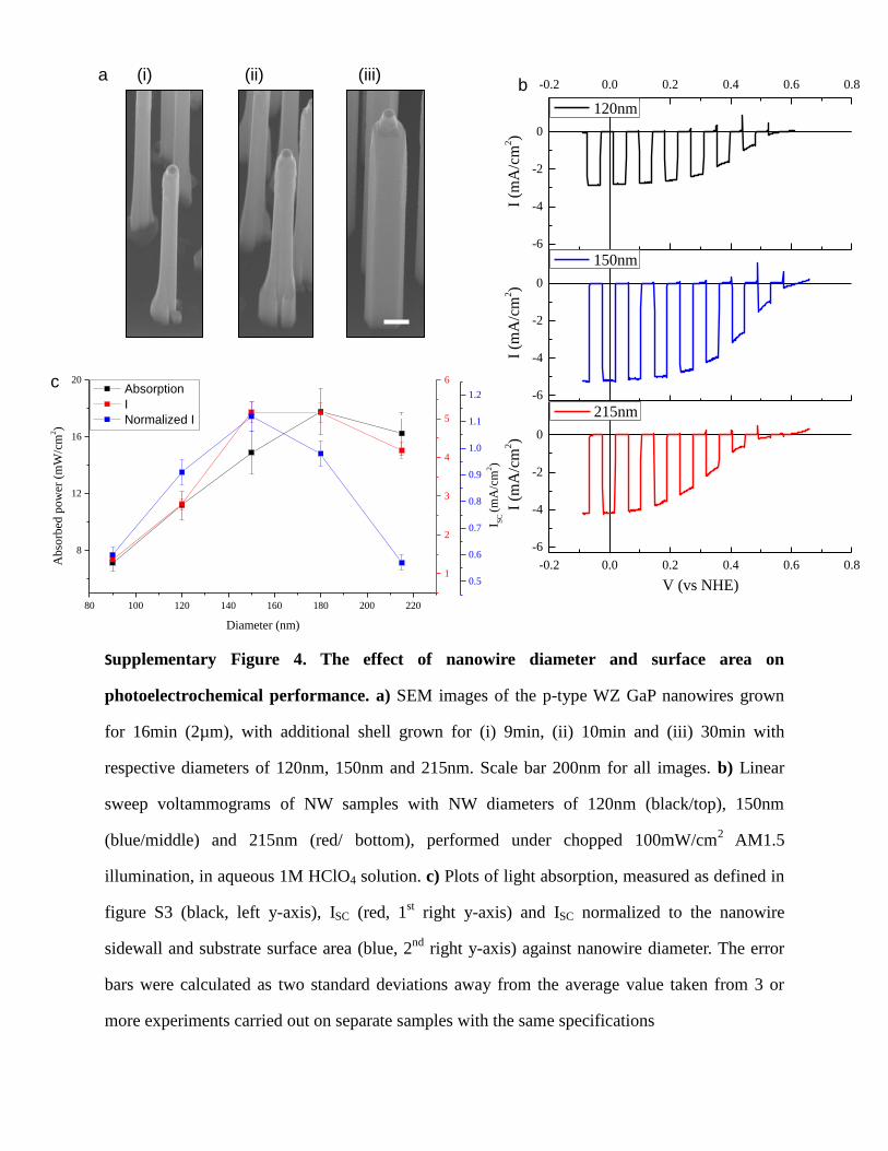
Supplementary Figure 4. The effect of nanowire diameter and surface area on
photoelectrochemical performance. a) SEM images of the p-type WZ GaP nanowires grown
for 16min (2µm), with additional shell grown for (i) 9min, (ii) 10min and (iii) 30min with
respective diameters of 120nm, 150nm and 215nm. Scale bar 200nm for all images. b) Linear
sweep voltammograms of NW samples with NW diameters of 120nm (black/top), 150nm
(blue/middle) and 215nm (red/ bottom), performed under chopped 100mW/cm2 AM1.5
illumination, in aqueous 1M HClO4 solution. c) Plots of light absorption, measured as defined in
figure S3 (black, left y-axis), ISC (red, 1st right y-axis) and ISC normalized to the nanowire
sidewall and substrate surface area (blue, 2nd
right y-axis) against nanowire diameter. The error
bars were calculated as two standard deviations away from the average value taken from 3 or
more experiments carried out on separate samples with the same specifications
80 100 120 140 160 180 200 220
8
12
16
20
Ab
sorb
ed p
ow
er (
mW
/cm
2)
Absorption
I
Normalized I
Diameter (nm)
1
2
3
4
5
6
IS
C (m
A/c
m2)
0.5
0.6
0.7
0.8
0.9
1.0
1.1
1.2
-6
-4
-2
0
-0.2 0.0 0.2 0.4 0.6 0.8
-6
-4
-2
0
-0.2 0.0 0.2 0.4 0.6 0.8
-6
-4
-2
0
I (m
A/c
m2)
120nm
I (m
A/c
m2)
150nm
I (m
A/c
m2)
V (vs NHE)
215nm
a (i) (ii) (iii) b
c
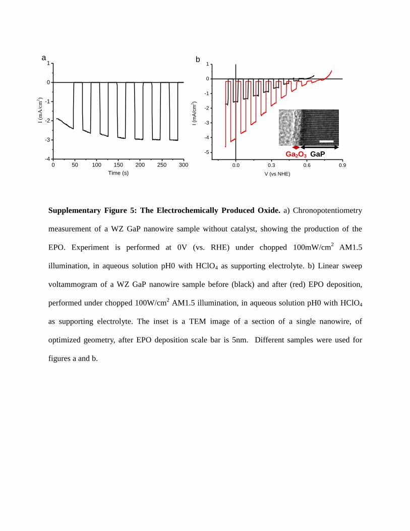
Supplementary Figure 5: The Electrochemically Produced Oxide. a) Chronopotentiometry
measurement of a WZ GaP nanowire sample without catalyst, showing the production of the
EPO. Experiment is performed at 0V (vs. RHE) under chopped 100mW/cm2 AM1.5
illumination, in aqueous solution pH0 with HClO4 as supporting electrolyte. b) Linear sweep
voltammogram of a WZ GaP nanowire sample before (black) and after (red) EPO deposition,
performed under chopped 100W/cm2 AM1.5 illumination, in aqueous solution pH0 with HClO4
as supporting electrolyte. The inset is a TEM image of a section of a single nanowire, of
optimized geometry, after EPO deposition scale bar is 5nm. Different samples were used for
figures a and b.
0.0 0.3 0.6 0.9
-5
-4
-3
-2
-1
0
1
I (m
A/c
m2)
V (vs NHE)
0 50 100 150 200 250 300-4
-3
-2
-1
0
1
I (m
A/c
m2)
Time (s)
a
GaP Ga2O3
b
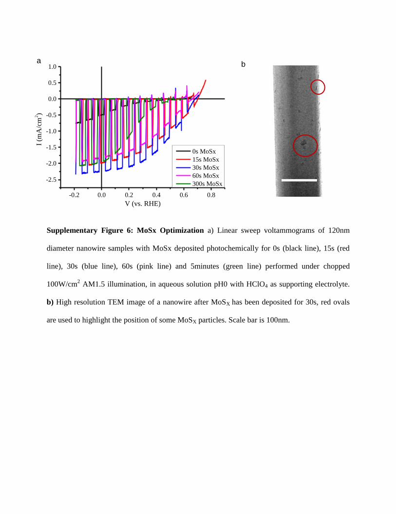
Supplementary Figure 6: MoSx Optimization a) Linear sweep voltammograms of 120nm
diameter nanowire samples with MoSx deposited photochemically for 0s (black line), 15s (red
line), 30s (blue line), 60s (pink line) and 5minutes (green line) performed under chopped
100W/cm2 AM1.5 illumination, in aqueous solution pH0 with HClO4 as supporting electrolyte.
b) High resolution TEM image of a nanowire after MoSX has been deposited for 30s, red ovals
are used to highlight the position of some MoSX particles. Scale bar is 100nm.
-0.2 0.0 0.2 0.4 0.6 0.8
-2.5
-2.0
-1.5
-1.0
-0.5
0.0
0.5
1.0
I (m
A/c
m2)
V (vs. RHE)
0s MoSx
15s MoSx
30s MoSx
60s MoSx
300s MoSx
a b
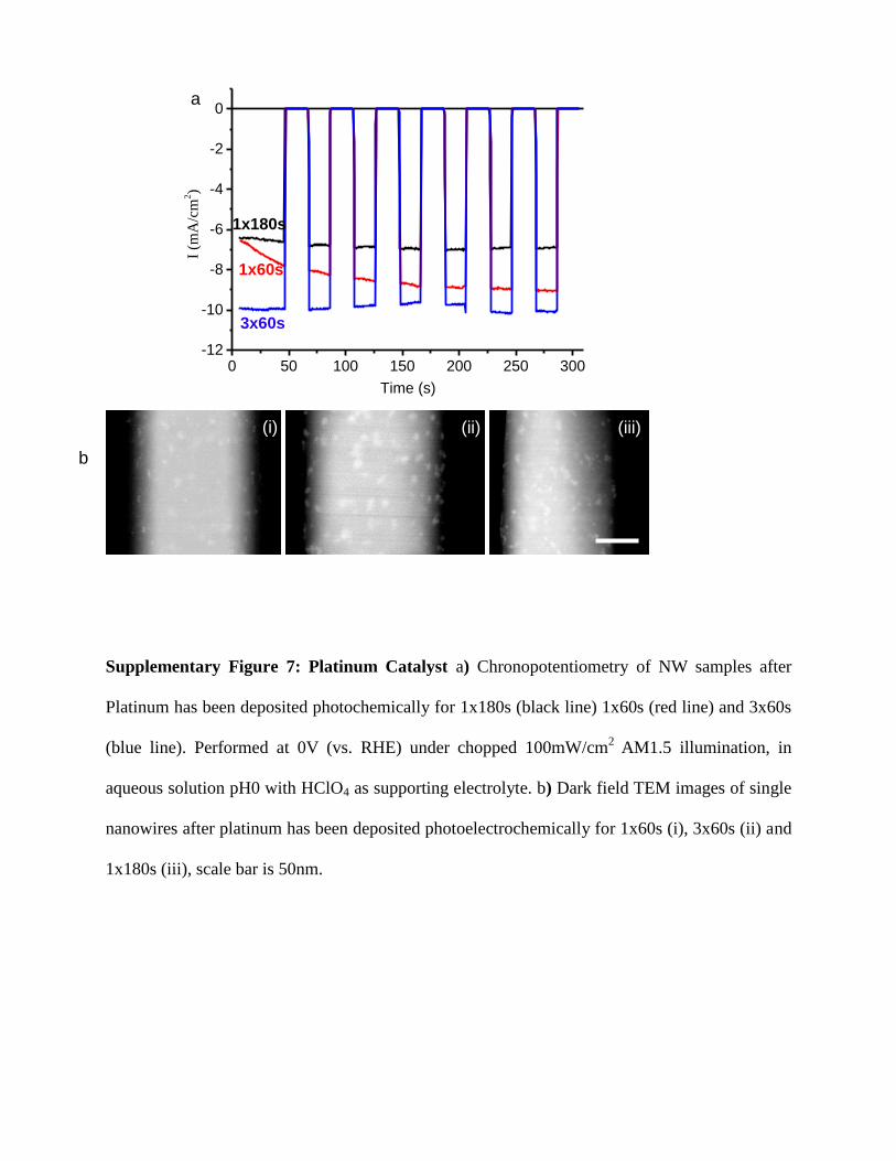
Supplementary Figure 7: Platinum Catalyst a) Chronopotentiometry of NW samples after
Platinum has been deposited photochemically for 1x180s (black line) 1x60s (red line) and 3x60s
(blue line). Performed at 0V (vs. RHE) under chopped 100mW/cm2 AM1.5 illumination, in
aqueous solution pH0 with HClO4 as supporting electrolyte. b) Dark field TEM images of single
nanowires after platinum has been deposited photoelectrochemically for 1x60s (i), 3x60s (ii) and
1x180s (iii), scale bar is 50nm.
0 50 100 150 200 250 300-12
-10
-8
-6
-4
-2
0
I (m
A/c
m2)
Time (s)
1x60s
3x60s
1x180s
a
b
(i) (ii) (iii)
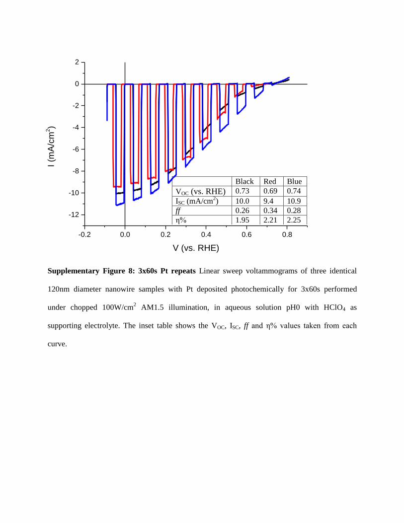
Supplementary Figure 8: 3x60s Pt repeats Linear sweep voltammograms of three identical
120nm diameter nanowire samples with Pt deposited photochemically for 3x60s performed
under chopped 100W/cm2 AM1.5 illumination, in aqueous solution pH0 with HClO4 as
supporting electrolyte. The inset table shows the VOC, ISC, ff and η% values taken from each
curve.
Black Red Blue
VOC (vs. RHE) 0.73 0.69 0.74
ISC (mA/cm2) 10.0 9.4 10.9
ff 0.26 0.34 0.28
η% 1.95 2.21 2.25
-0.2 0.0 0.2 0.4 0.6 0.8
-12
-10
-8
-6
-4
-2
0
2
I (m
A/c
m2)
V (vs. RHE)
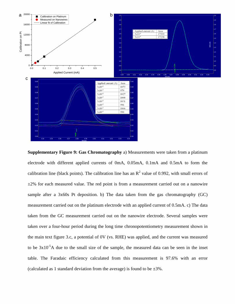
Supplementary Figure 9: Gas Chromatography a) Measurements were taken from a platinum
electrode with different applied currents of 0mA, 0.05mA, 0.1mA and 0.5mA to form the
calibration line (black points). The calibration line has an R2 value of 0.992, with small errors of
±2% for each measured value. The red point is from a measurement carried out on a nanowire
sample after a 3x60s Pt deposition. b) The data taken from the gas chromatography (GC)
measurement carried out on the platinum electrode with an applied current of 0.5mA. c) The data
taken from the GC measurement carried out on the nanowire electrode. Several samples were
taken over a four-hour period during the long time chronopotentiometry measurement shown in
the main text figure 3.c, a potential of 0V (vs. RHE) was applied, and the current was measured
to be 3x10⁻⁵
A due to the small size of the sample, the measured data can be seen in the inset
table. The Faradaic efficiency calculated from this measurement is 97.6% with an error
(calculated as 1 standard deviation from the average) is found to be ±3%.
Minutes
0.34 0.35 0.36 0.37 0.38 0.39 0.40 0.41 0.42 0.43 0.44
Mill
ivolts
0.30
0.31
0.32
0.33
0.34
0.35
0.36
0.37
0.38
0.39
0.40
Mill
ivolts
0.30
0.31
0.32
0.33
0.34
0.35
0.36
0.37
0.38
0.39
0.40
He
/H2
10
73
0.0 0.1 0.2 0.3 0.4 0.5
0
4000
8000
12000
16000
20000
Calibration on Platinum
Measured on Nanowires
Linear fit of CalibrationC
alib
ration o
n P
t
Applied Current (mA)
a
b a
Minutes
0.29 0.30 0.31 0.32 0.33 0.34 0.35 0.36 0.37 0.38 0.39 0.40 0.41 0.42 0.43
Mill
ivolts
0.8
0.9
1.0
1.1
1.2
1.3
1.4
1.5
1.6
1.7
1.8
1.9
2.0
Mill
ivolts
0.8
0.9
1.0
1.1
1.2
1.3
1.4
1.5
1.6
1.7
1.8
1.9
2.0
He
/H2
17
25
8
c
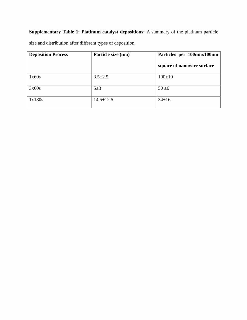
Supplementary Table 1: Platinum catalyst depositions: A summary of the platinum particle
size and distribution after different types of deposition.
Deposition Process Particle size (nm) Particles per 100nmx100nm
square of nanowire surface
1x60s 3.5±2.5 100±10
3x60s 5±3 50 ±6
1x180s 14.5±12.5 34±16
Supplementary note 1. Geometry optimization
1.1 Wire Length:
In the following sections we will discuss the geometry optimization, and catalyst deposition steps
studied to reach high efficiency. We first study the effect of wire length. Supplementary figure
2.a shows SEM images of wires with different lengths without catalysts. In supplementary figure
2.b the I-V behavior, of wires with lengths 0.73µm, 2.02µm and 3.5µm and a constant diameter
of 90nm, is shown. The shortest wires (0.73µm, black line/ top panel) exhibit the highest VOC,
however, when the length is increased to 2.02µm (blue line/ middle panel), the ISC and ff
improve, with only a small decrease in VOC. With a further increase in length to 3.5µm (red line/
bottom panel) a dramatic decrease is observed in VOC, ISC and ff, however the saturation current
appears unchanged. In supplementary figure 2.c the measured series resistance in the system,
obtained from impedance measurements, in the dark (black points, left axis), and the ISC, under
illumination (red points, right axis), are plotted. The lines connecting the points in supplementary
figure 2.c are only added as a guide to the eye. In supplementary figure 2.c (black points) we see
that resistance increases greatly as nanowire length increases, as is expected from the equation;
ALR (3)
where R is the resistance of the wire, ρ is the resistivity of the material, L is the wire length, and
A is the wire cross sectional area. However this is clearly not the only factor affecting
performance as the trend for ISC is not the inverse of resistance. This is due to the light absorption
increasing with nanowire length (supplementary figure 3). Due to the increased surface area, the
flux of electrons through the electrode electrolyte junction per unit area decreases. This causes a
decrease in the quasi-Fermi level, and therefore VOC2–4
. The change in VOC can be calculated by
0
lnI
I
q
TkV SCB
OC
(4)
where γ is the actual junction area and I0 is the saturation current density. This factor, however,
only accounts for a small decrease in VOC on the order of 10s of mV, the further drop in voltage
is due to the resistance and length of the nanowire. As the nanowire length continues to increase,
more voltage is lost due to the increased resistance and surface area, causing the decrease in ISC
observed in supplementary figure 2.c, and the change in the I-V curve shape observed in
supplementary figure 2.b. It is found that the optimum wire length is 2µm, yielding promising
VOC and ffs; this wire length allows for good transport of charge carriers and reasonable
absorption of light without too much voltage drop from the increased resistance and surface area.
The ISC, however, should be able to reach a much larger value of up to the previously mentioned
value of; 12.5mA/cm2.
1.2 Wire diameter:
Using the optimized wire length, the effect of the wire diameter is studied by growing a
shell on the wires, maintaining the pure WZ crystal structure, with nominally the same dopant
concentration as used for the growth of the core. Average wire diameters of 90nm, 120nm,
150nm, 180nm and 215nm are obtained by respective shell growth times of 0, 5, 10, 20 and 30
minutes. Supplementary figure 4.a shows the SEM images of the wires with 5, 10, and 30 minute
shell growth times. It is evident from these SEM images that the wire length also increases with
shell growth; this is due to unavoidable axial growth through the catalytic gold particle from the
initial VLS growth. Supplementary figure 4.b shows the I-V behavior of the samples with growth
times of; 5 minutes (black line/ top panel), 10 minutes (blue line/ middle panel) and 30 minutes
(red line/ bottom panel). Very little change in VOC and ff is observed with increasing the diameter
from 90nm to 180nm; however the ff does decrease with a further increase in diameter to 215nm.
The VOC does not decrease with the increased surface area as would be expected, this is due to
the resistance, as observed from impedance measurements, decreasing as the diameter increases,
leading to a decrease in the resistance dependant voltage drop, allowing the two effects cancel
each other out. The ISC on the other hand increases dramatically from 1.5mA/cm2 to over
5mA/cm2, reaching a plateau for wire diameters of 150-180 nm and decreasing for the thickest
wires. This trend in ISC is shown by the red points in supplementary figure 4.c (the line is added
as a guide to the eye). The blue plot shows the same data, but with the ISC normalized to the
nanowire surface area (again the line is added as a guide to the eye). From the ISC and normalized
ISC plots it is apparent that for WZ GaP the optimum nanowire diameter, for PEC applications, is
150nm. This is an unexpected result, as our absorption measurements show an optimum
absorption at 180nm (supplementary figure 4.c black plot). A decrease in absorption occurs at
diameters greater than 180nm as reflection starts to occur at the top of the array5. Besides light
absorption, bulk recombination also becomes a factor as the nanowire diameter increases past
double the space charge width (as calculated in supplementary figure 1), resulting in a lower ISC
than expected for the larger nanowire diameters. The ISC decreases further with diameter as the
average refractive index is increased causing reflection to become an issue. A possible further
reason for the lower ISC from the thicker nanowires is the axial growth caused by the gold
particle during shell growth. As the axial growth is not intentional during this growth phase
stacking faults are incorporated, which could lead to recombination of charge carriers, and a
lower than expected ISC.
Supplementary note 2. Electrochemically Produced Oxide (EPO)
Due to the large surface area of the 2µm long 150nm wide nanowires, an oxide layer can help to
passivate surface states6–8
, reducing surface recombination. A simple method for the production
of an oxide layer is to apply a reducing potential to the GaP electrode while under illumination in
an aqueous acid. The surface of the GaP will be reduced to gallium metal and phosphine. The
gallium metal is then quickly oxidized by the aqueous acid to gallium oxide, thus forming an
electrochemically produced oxide (EPO), similarly to the process observed on InP7. The
formation of this EPO layer can be observed during electrochemical measurements, by the
increase observed in the current. The chronopotentiometry measurement shown in
supplementary figure 5.a demonstrates this clearly. In the first 150 seconds the current increases
as the oxide layer is formed. Once the oxide layer is conformal over the surface of the nanowire
the current stabilizes, and remains stable for the following 150 seconds. The experiment in
supplementary figure 5.a is carried out under chopped illumination so that the dark current can
also be observed. The fact that the dark current does not increase during the experiment shows
that the current under illumination is purely due to the passivating effect of the oxide layer and
not due to any surface charging, as that would also cause the dark current to increase.
Supplementary Figure 5.b shows the I-V behavior of the nanowires after the production of the
EPO layer, the ISC and VOC are both increased to 4.1mA/cm2 and 0.75V (vs. RHE) respectively.
The inset in this figure shows a TEM image of a section of a nanowire after the production of the
EPO layer. The EPO layer is observed to be approximately 3nm in thickness, and is clearly not
evident prior to the electrochemical treatment in figure 1.c in the main text. This EPO passivates
surface states6–8
, decreasing surface recombination, leading to the observed increase in current.
In the presence of the EPO the ISC is still limited to ~4mA, so a catalyst should still be
implemented to promote charge transfer further.
Supplementary note 3. Catalyst deposition
Supplementary figure 7.a shows chronopotentiometry measurements performed on the
nanowire samples after a single 180s deposition (black line), a single 60s deposition (red line)
and after 3 consecutive 60s depositions (blue line). During the chronopotentiometry
measurements, after a single 60s deposition (red line), an increase in current is observed over
time. The increase is, however, not observed after 3 consecutive 60s depositions (blue line), and
only a slight increase is observed for the 180s deposition (black line). It can be seen from
supplementary figure 5 that the oxide layer increases slightly in thickness after 3 consecutive
platinum depositions. When the platinum coverage is low, as is the case for 1x60s (and to a
lesser extent for 1x180s), reactions will still occur on the nanowire surface without the aid of the
catalyst. This, has in this case, lead to the oxide being reduced back to gallium metal, and
exposing the GaP surface, allowing for the production of a thicker (passivating) oxide layer,
which will act to reduce surface recombination and therefore increase current. Once the catalyst
loading is high enough, as is the case for 3x60s, the catalyst particles are used preferentially for
charge transfer from the semiconductor to the electrolyte, allowing for an increased reaction rate.
The preferential use of the catalyst particles for charge transfer will also reduce the chance of
oxide layer removal and surface reduction, leading to the reasonable stability observed in figure
3.c.
Supplementary References
1. Standing, a J., Assali, S., Haverkort, J. E. M. & Bakkers, E. P. a M. High yield transfer of
ordered nanowire arrays into transparent flexible polymer films. Nanotechnology 23,
495305 (2012).
2. Sim, U., Jeong, H.-Y., Yang, T.-Y. & Nam, K. T. Nanostructural dependence of hydrogen
production in silicon photocathodes. J. Mater. Chem. A 1, 5414–5422 (2013).
3. Maiolo, J. R., Atwater, H. a. & Lewis, N. S. Macroporous Silicon as a Model for Silicon
Wire Array Solar Cells. J. Phys. Chem. C 112, 6194–6201 (2008).
4. Osterloh, F. E. Inorganic nanostructures for photoelectrochemical and photocatalytic
water splitting. Chem. Soc. Rev. 42, 2294–320 (2013).
5. Kupec, J., Stoop, R. & Witzigmann, B. Light absorption and emission in nanowire array
solar cells. Opt. Express 18, 27589–27605 (2010).
6. Panda, J., Roy, A., Gemmi, M. & Husanu, E. Electronic Band Structure of Wurtzite GaP
Nanowires via Resonance Raman Spectroscopy. J. Am. Chem. Soc. 135, 1057–1064
(2013).
7. Munoz, a. G. et al. Photoelectrochemical Conditioning of MOVPE p-InP Films for Light-
Induced Hydrogen Evolution: Chemical, Electronic and Optical Properties. ECS J. Solid
State Sci. Technol. 2, Q51–Q58 (2013).
8. Esposito, D. V, Levin, I., Moffat, T. P. & Talin, a A. H2 evolution at Si-based metal-
insulator-semiconductor photoelectrodes enhanced by inversion channel charge collection
and H spillover. Nat. Mater. 12, 562–8 (2013).