Embed Size (px)
Citation preview

VCE Physics
Unit 3
Electronics &
Photonics

1.0 Unit Outline• apply the concepts of current, voltage, power to the operation of electronic
circuits comprising diodes, resistance, and photonic transducers including light dependent resistors (LDR), photodiodes and light emitting diodes (LED);
• simplify circuits comprising parallel and series resistance and unloaded voltage dividers;
• describe the operation of a transistor in terms of current gain and the effect of biasing on the voltage characteristics in terms of saturation, cut-off and linear operation, including linear gain (∆Vout/∆Vin) and clipping of a single stage npn transistor voltage amplifier;
• explain qualitatively how capacitors act as de-couplers to separate AC from DC signals in transistor circuits;
• use technical specifications related to voltage, current, resistance, power and illumination for electronic components such as diodes, resistance, and opto-electronic converters including light dependent resistors (LDR), photodiodes and light emitting diodes (LED), excluding current–voltage characteristic curves for transistors, to design circuits to operate for particular purposes;
• analyse simple electronic transducer circuits for transducers that respond to changes in illumination and temperature including LDR, photodiode, phototransistor and thermistor;
• describe energy transfers and transformations in electrical–optical, and optical–electrical conversion systems using opto-electronic converters;
• describe the transfer of information in analogue form using optical intensity modulated light;
• use safe and responsible practices when working with electrical, electronic and photonic equipment.

Chapter 1
• Topics covered:
• Electric Charge.
• Electric Current.
• Voltage.
• Electromotive Force.
• Electrical Energy.
• Electric Power.

1.0 Electric Charge• The fundamental unit of electrical
charge is that carried by the electron
(& the proton).
• This is the smallest discrete charge
known to exist independently and is
called the ELEMENTARY CHARGE.
• Electric Charge (symbol Q) is
measured in units called COULOMBS
(C).
• The electron carries - 1.6 x 10⁻¹⁹ C.
• The proton carries +1.6 x 10⁻¹⁹ C.
If 1 electron carries 1.6 x 10⁻¹⁹ CThen the number of electrons in 1 Coulomb of Charge
= 1 C 1.6 x 10-19 = 6.25 x 10¹⁸ electrons

1.1 Flowing Charges• When electric charges (in particular
electrons) are made to move or “flow”, an Electric Current (symbol I) is said to exist.
• The SIZE of this current depends upon the NUMBER OF COULOMBS of charge passing a given point in a given TIME.
Section of Current Carrying Wire
Mathematically:
I = Q/t where: I = Current in Amperes (A) Q = Charge in Coulombs (C) t = Time in Seconds (s)
If 1 Amp of current is flowing past this point,
then 6.25 x 10¹⁸ electrons pass here every second.

1.2 Electric Current• Electric CURRENTS usually flow along
wires made from some kind of CONDUCTING MATERIAL, usually, but not always, a METAL.
• Currents can also flow through a Liquid (electrolysis), through a Vacuum (old style radio “valves”), or through a Semiconductor (Modern Diodes or Transistors).
• A Current can only flow around a COMPLETE CIRCUIT.
• A break ANYWHERE in the circuit means the current stops flowing EVERYWHERE, IMMEDIATLY.
• The current does not get weaker as it flows around the circuit, BUT REMAINS CONSTANT.
• It is the ENERGY possessed by the electrons (obtained from the battery or power supply) which gets used up as the electrons move around the circuit.
• In circuits, currents are measured with AMMETERS, which are connected in series with the power supply.
Typical Electric Circuit
ConnectingWires
Resistor (consumes energy)
BatteryCurrent
A
Measures Current Flow

1.3 Conventional Current vs Electron Current
Positive Terminal Negative Terminal
Conventional vs Electron Current
Resistor
Electron Current: Never shown on Circuit Diagrams
Conventional Current:Always shown on Circuit Diagrams
Well before the discovery of the electron, electric currents were known to exist.
It was thought that these currents were made up of a stream of positive particles and their direction of movement constituted the direction of current flow around a circuit.
This meant that in a Direct Current (D.C.) circuit, the current would flow out of the POSITIVE terminal of the power supply and into the NEGATIVE terminal.Currents of this kind are called Conventional Currents, and ALL CURRENTS SHOWN ON ALL CIRCUIT DIAGRAMS EVERYWHERE are shown as Conventional Current, as opposed to the “real” or ELECTRON CURRENT.

1.4 Voltage• To make a current flow around a
circuit, a DRIVING FORCE is required.
• This driving force is the DIFFERENCE in VOLTAGE (Voltage Drop or Potential Difference) between the start and the end of the circuit.
• The larger the current needed, the larger the voltage required to drive that current.
• VOLTAGE is DEFINED as the ENERGY SUPPLIED TO THE CHARGE CARRIERS FOR THEM TO DO THEIR JOB ie.TRAVEL ONCE AROUND THE CIRCUIT.
• So, in passing through a Voltage of 1 Volt, 1 Coulomb of Charge picks up 1 Joule of Electrical Energy.
• OR • A 12 Volt battery will supply each
Coulomb of Charge passing through it with 12 J of Energy.
Mathematically;
V = W/q where: V = Voltage (Volts) W = Electrical Energy (Joules) q = Charge (Coulombs)
Alessandro Volta

1.5 E.M.F. Voltage is measured with a VOLTMETER.
The term EMF (ELECTROMOTIVE FORCE) describes a particular type of voltage.It is the VOLTAGE of a battery or power supply when NO CURRENT is being drawn.
This is called the “Open Circuit Voltage” of the battery or supply
V
VoltmeterCircuit Symbol
With S closed, a current begins to flow and V drops and now measures voltage available to drive the current through the external circuit
Resistor
A
V
S
V measures EMF
Voltmeters are placed in PARALLEL with the device whose voltage is being measured.Voltmeters have a very high internal resistance, so they have little or no effect the operation of the circuit to which they are attached.
Resistor
A
V

1.6 Electrical Energy
The conversion of Electrical Energy when a current passes through a circuit element (a computer) is shown below.
Mathematically W = VQ ………1, where: W = Electrical energy (Joule) V = Voltage (Volts) Q = Charge (Coulomb)
Current and Charge are related through: Q = It. substituting for Q, in equation 1 we get: W = VIt
Voltage = V volts
Charges (Q) enter with high energy
Charges (Q) leave with low energy
Q Coulombs of Electricity enter
computer
Q Coulombs of Electricity leave
computer
In time t, W units of energy are transformed to heat and light
Electrical Energy (W) is defined as the product of the Voltage (V) across, times the Charge (Q), passing through a circuit element (eg. a light globe).

1.7 Electrical Power• Electrical Power is DEFINED as the
Time Rate of Energy Transfer:
P = W/t where P = Power (Watts, W) W = Electrical Energy (Joule) t = Time (sec)
• From W = VI t we get:
P = VI • From Ohm’s Law (V = IR) [see next
chapter] we get:
P = VI = I2R = V2/R where: I = Current (Amps)
R = Resistance (Ohms) V = Voltage (Volts)
Electrical Power is sold to consumers in units of Kilowatt-Hours. (kW.h)
A 1000 W (1kW) fan heater operating for 1 Hour consumes 1kWh of electrical power.
Since P = W/t or W = P x t, we can say:
1 Joule = 1 Watt.sec
so
1000 J = 1kW.sec
so
3,600,000 J = 1 kW.hour
or
3.6 MJ = 1 kW.h

1.8 A.C. Electricity• There are two basic types of current
electricity:
(a) D.C. (Direct Current) electricity where the current flows in one direction only.
(b) A.C. (Alternating Current) where the current changes direction in a regular and periodic fashion.
• The Electricity Grid supplies domestic and industrial users with A.C. electricity.
• A.C. is favoured because:
(a) it is cheap and easy to generate
(b) it can be “transformed”; its voltage can be raised or lowered at will by passage through a transformer.
• The only large scale use of high voltage D.C. electricity is in public transport, ie. trams and trains.
Voltage
Time
VP VPtoP
T
A.C. ELECTRICITY - PROPERTIES
VPtoP = “Peak to Peak Voltage”
for Domestic Supply VPtoP = 678 V
T = “Period”for Domestic Supply T = 0.02 sec
VP = “Peak Voltage” for Domestic Supply VP = 339 V

1.9 R.M.S. Voltage and Current
V
t339
-339
0
V2
t
1.15 x 10⁵
0 0
Mean V2
5.8 x 10⁴
t0
Mean V2
240 t
GRAPHICAL DEVELOPMENT OF THE RMS VOLTAGE FROM AN A.C. VOLTAGE
With an A.C. supply, the average values for both voltage and current = 0,
so Vav and Iav cannot be used by the Power Companies to calculate the amount of electric power consumed by its customers.
To get around this problem R.M.S. or Root Mean Square values for AC voltage and current were developed.
RMS values are DEFINED as: The AC Voltage/Current which delivers the same voltage/current to an electrical device as a numerically equal D.C. supply would deliver.An AC source operating at 240 V RMS delivers the same power to a device as a DC source of 240 V.
Yet, AC circuits do consume power, so a method of calculating it had to be found.

1.10 Peak versus RMS Values• In AC supplies, the Peak
and RMS values are related through simple formulae:
• For Voltage:
VRMS = VP/2
• For Current:
IRMS = IP/2
• In Australia Domestic Electricity is supplied at 240 V, 50 Hz
• The Voltage quoted is the RMS value for the AC supply.
• Thus the Peak value for voltage is
VP = VRMS x 2 = 240 x 1.414 = 339 V
Voltage (V)
Time (s)
VP
+339 V
- 339 V
VP to P
240 V

Chapter 2
• Topics covered:
• Resistance.
• Ohm’s Law.
• Resistors in Series and Parallel.
• Voltage Dividers
• Impedance Matching

2.0 Resistance• Electrical Resistance is a property of
ALL materials, whether they be classed as conductors, insulators or something in between. (ie Semiconductors)
• The size of the resistance depends upon a number of factors:
(a) The nature of the material. This is measured by “resistivity” ()
(b) The length, L, of the material.
(c) The cross sectional area, A, of the material.
COMPARING RESISTANCE
L
A 2
A 1
Wires 1 and 2 are made from the same material
Wire 1 has ½ the cross sectionalarea of Wire 2
Wire 1 has TWICE the resistance of Wire 2
Combining these mathematically:
R = L/A where:R = Resistance (Ohms) = Resistivity (Ohm.m) .m L = Length (m) A = Cross Sectional Area (m2)

2.1 Ohm’s Law• OHM’S LAW relates the Voltage
across, the Current through and the Resistance of a conductor.
• Mathematically:
V = IR where: V = Voltage (Volts) I = Current (Amps) R = Resistance (Ohms)
• Any conductor which follows Ohm’s Law is called an OHMIC CONDUCTOR.
Ohm’s Law - Graphically
V
I
A graph of V versus I produces a straight line with Slope = R(Remember a straight line graph has formula y = mx + c)
The graph is a straight line, the Resistance of Device 1 is CONSTANT (over the range of values studied).
The slope indicates Device 2has a lower (but still constant)Resistance when compared to Device 1.
Slope = RDevice 1
Slope = RDevice 2
Georg Ohm
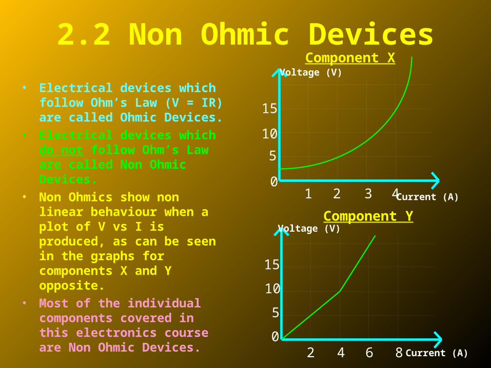
2.2 Non Ohmic Devices
• Electrical devices which follow Ohm’s Law (V = IR) are called Ohmic Devices.
• Electrical devices which do not follow Ohm’s Law are called Non Ohmic Devices.
• Non Ohmics show non linear behaviour when a plot of V vs I is produced, as can be seen in the graphs for components X and Y opposite.
• Most of the individual components covered in this electronics course are Non Ohmic Devices.
Voltage (V)
Current (A)
Component Y
0
5
10
15
2 4 6 8
Current (A)
Voltage (V) Component X
0
5
10
15
1 2 43

2.3 Resistors in Series• Conductors which exhibit a
resistance to current flow are generally called RESISTORS.
• When connected “end to end” or in “SERIES”, the total resistance of the combination = the sum of the individual resistances of the resistors in the “network”.
• Mathematically: RT = R1 + R2 + R3 + … …
IN A SERIES CIRCUIT:(a) Since only ONE pathway around the circuit exists, the current through each resistor is the same.
Thus: I = I1 = I2 = I3
Resistors in SERIES
These three resistors can be replaced by a single resistor of value
RT = R1 + R2 + R3
R1R2 R3
V
V1V2 V3
Resistors in a Series Circuit
(b) The sum of the voltage drops across the resistors = the voltage of the power supply,
Thus: V = V1 + V2 + V3
I
I1 I2I3
The greater the number of resistors in a series network the greater thevalue of the equivalent resistance (RT)
R1 R2 R3
RT

2.4 Resistors in Parallel• Resistors connected “side by side”
are said to be connected in “PARALLEL”.
• The total resistance of a parallel network is found from adding the reciprocals of the individual resistances.
IN A PARALLEL CIRCUIT:(a) The current through each arm varies.
Thus: I = I1 + I2 + I3
R3
R2
R1
These three Resistors can be replaced by a single Resistor ( RT )
Resistors in Parallel
Resistors in a Parallel Circuit
R3
R2
R1
V
I3
I2
I1
I
V1
V3
V2
(b) The voltage drop across each arm is the same. Thus: V = V1 = V2 = V3
The greater the number of resistors in a parallel network the lower the value of the equivalent resistance (RT).
Mathematically: 1/RT = 1/R1 + 1/R2 + 1/R3
RT

2.5 Voltage Dividers - 1
For the circuit above:
V = V1 + V2
Since this is a series circuit ,
the current ( I ) is the same everywhere:
I = V1/R1 and I = V2/R2
So V1/V2 = R1/R2
R1V1
R2V2
V
I
Suppose you have a 12 V battery, but you need only 4 V to power your circuit. How do you get around this problem ?You use a Voltage Divider Circuit.
They are made by using combinations of fixed value resistors or using variable resistors called rheostats.
Voltage dividers are one of the most important circuits types used in electronics. Almost all sensor subsystems (eg Thermistors, LDR’s), use voltage divider circuits, there is just no other way to convert the sensor inputs into useful “electrical” information.

2.6 Voltage Dividers - 2
If the main voltage supply (V) is connected across the ends of the rheostat, then the voltage required by RL is tapped between A and the position of the slider.
V
A
Rheostat
RL
Slider
The further from A the slider moves the larger the voltage drop across the load resistor , RL
Using rheostats, the a voltage divider can be set up as shown.
Slider type rheostat
Various rotary rheostats

2.7 Voltage Divider Formula
For the VOUT circuit:
VIN = I (R1 + R2)
VIN CircuitVOUT CircuitR1
R2
VIN
VOUT
I
For the VIN circuit: Applying Ohm’s Law
The Voltage divider circuit is a SERIES circuit.Thus, the SAME CURRENT flows EVERYWHEREIn other words, the SAME CURRENT flows through R1 AND R2
I = VIN
(R1 + R2) …….(1)
VOUT = IR2
I = VOUT
R2
……..(2)
Combining 1 and 2 we get:VOUT = VIN R2 (R1 + R2)
so, VOUT = VIN.R2
(R1 + R2)
This is the Voltage Divider Formula

2.8 Impedance Matching 1IMPEDANCE is the TOTAL resistance to current flow due to ALL the components in a circuit. In Voltage Divider circuits we only have resistors,
so Total Impedance = Total Resistance.
The current (I) in the circuit is: I = V/RT = 12/1200 = 0.01 A.
In the circuit shown a supply of 12 V is connected across 2 resistors of 500 and 700 in series.
I
R2V2
V
R1V17 V
5 V 500
700 Ω
12
The Voltage Drop across R1 = I x R1
= 0.01 x 700 = 7.0 V
The Voltage Drop across R2
= I x R2
= 0.01 x 500 = 5.0 V

CASE (b): Now RL = 5000 , Then RT = (1/500 + 1/5000)-1 = 454.5 and I = V/RT = 0.011 A.This is only a 10 % increase in current.
CASE (a): Suppose RL has a total impedance of 50
RL and R2 are in parallel, so Total Resistance RT for the parallel network = (1/R2 + 1/RL)-1
= (1/500 + 1/50)-1 = 45.5 I = V/RT = 5.0/45.5 = 0.11 A. This is an 110% increase in the current in the circuit. This will cause a dangerous heating effect in R1 and also decrease the Voltage across RL - both undesirable events !
Suppose a load (RL), requires 5.0 V to operate.Conveniently, 5 V appears across R2.
2.9 Impedance Matching 2
I
R2V2
V
R1V1
500
700 Ω
12
7 V
5 V RL 50 5 V
In other words it is important to “match” the impedance of the load RL to that of resistor R2 such that: RL 10R2
5 V 500 5000
Lets look at 2 cases where the impedance of RL varies.

Chapter 3.
• Topics covered:
• Semiconductors
• Diodes
• p-n junctions
• Forward & Reverse Bias
• Capacitors

3.0 Semiconductors• Most electronic devices, eg. diodes,
thermistors, LED’s and transistors are “solid state semi conductor” devices.
• “Solid State” because they are made up of solid materials and have no moving parts.
• “Semiconductor” because these materials fall roughly in the middle of the range between Pure Conductor and Pure Insulator.
• Semiconductors are usually made from Silicon or Germanium with impurities deliberately added to their crystal structures.
• The impurities either add extra electrons to the lattice producing n type semiconductor material.
N - Type Semiconductor
Si Si
Si Si
P Si
Si Si
extra electron
P - Type Semiconductor
Si Si
Si Si
B Si
Si Si
hole
or create a deficit of electrons (called “holes”) in the lattice producing p type semiconductor material.Holes are regarded as positive (+) charge carriers, moving through the lattice by having electrons jump into the hole leaving behind another hole.

3.1 p-n junctions
p n
Joining together p type and n type material produces a so called “p-n junction”
When brought together, electrons from the n type migrate to fill holes in the p type material.
np
np
As a result, a “depletion layer”, (an insulating region containing very few current carriers), is set up between the two materials.
depletion layer
The “majority” current carriers are holes in p type material and electrons in n type material.However, each also has some “minority” carriers (electrons in p, holes in n) due to impurities in the semiconductor and their dopeants
Note: undoped semiconductor material, pure silicon or germanium, is called “intrinsic semiconductor material”.

3.2 Forward and Reverse Bias
p n
depletion layer
it draws the charge carriers away from the junction and makes the depletion layer bigger meaning current is even less likely to flow and the junction is now “reverse biased”
p n
depletion layer
it draws the charge carriers toward the junction and makes the depletion layer smaller.
If an external supply is now connected as shown
The current carriers now have enough energy to cross the junction which now becomes “conducting” or “forward biased”
If the external supply is now reversed,

3.3 The Diode• Diodes are electronic devices made by sandwiching together n
type and p type semiconductor materials.• This produces a device that has a low resistance to current flow
in one direction, but a high resistance in the other direction.
Cathode (-)Anode (+)
Conventional Current Flow
Current (mA)
Voltage (V) 0.7 V
The “Characteristic Curve” (the I vs V graph) for a typical silicon diode is shown.
This diode will not fully conduct until a forward bias voltage of 0.7 V exists across it.
Notice that when the diode is reverse biased it does still conduct - but the current is in the pA or μA range. This current is due to minority carriers crossing what is for them a forward biased junction.
V (μA)
Circuit Symbol

Chapter 4
Topics Covered:•Capacitors•Capacitance•Charge Storage•Capacitors DC Blockers

4.0 CapacitorsPolarised
Metal Charge Storage Plates Connecting Wires
Dielectric orInsulator
100 uF
•The “sandwich” is then rolled into a cylinder and covered with a protective coating.
Capacitors are devices with the ability to temporarily store electrical charge.They are made from two plates of conducting material separated by a layer of insulation material, called a “dielectric”.
Non Polarised
Each plate has a wire attached which allows for the capacitor’s connection into a circuit.
Others are “non polarised”, it does not matter which way they are connected.
There are many different types of capacitors, some of which are “polarised”- they must be connected in a particular way.

4.1 Capacitance• The ability of capacitors to
store charge is called their CAPACITANCE.
• This capacitance of any capacitor is the ratio of the the amount of Charge (Q) the plates can carry to the Potential Difference or Voltage (V) between the plates.
• The unit of Capacitance is the FARAD.
• This is a very large unit so capacitance is often quoted in microfarads F (10-6F) or picofarads pF (10-12 F)
• Mathematically:
C = Q/V where:
C = Capacitance in Farads
Q = Charge in Coulombs
V = Potential Difference in Volts

4.2 Charge Storage
Current
Time Time
Charge on Plates
When the switch, S, is closed the current (I ) rises to a maximum rapidly. This forces charge onto the plates of the capacitor, as shown.
As the charge builds on the plates the voltage difference between the plates starts to rise until it reaches a maximum value equal to the EMF of the supply.
AV
SS
IIII = 0
This process is shown graphically below.
Time
Voltage across PlatesSupply
EMF
The charge on the plates mirrors the voltage across the plates as shown
Capacitors store charge. How do they perform in a circuit ? Let us set up a circuit to study their operation.
R
As the charge on the capacitor builds , the current flow becomes less until the capacitor becomes fully charged and the current stops completely.

4.3 Capacitors – DC BlockersAs can be seen from the previous slide, current will only flow for a short time in a capacitor circuit powered by a DC supply.Once the capacitor is fully charged the DC Current then stops flowing or is “blocked”
What happens when the DC supply is replaced by an AC supply ?Since the AC supply reverses direction regularly, the capacitor will not have time to fully charge.So it cannot stop the current flow before the supply has switched polarity and the current begins flowing in the reverse direction.
As far as the rest of the circuit elements are concerned; resistor, ammeter and the wires, it appears that the capacitor is not even present – it has no effect on the operation of the circuit.
R
CA
t
IR
Under AC conditions the Capacitor appears not to be there, i.e., it passes AC signals without affecting or changing them. In other words the capacitor acts like a short circuit.

Chapter 5
Topics Covered:
Input Transducers

5.0 Input TransducersTransducers are devices which convert non electrical signals into electrical signals.Input Transducers convert mechanical and other forms of energy eg. Heat, Light or Sound into Electrical Energy.
Light Emitting Diode (LED)
Light is emitted when the diode is forward biased
Light Dependent Resistor (LDR)
The resistance changes as
light intensity varies
Symbol
Examples of a few such devices are shown here.
Photodiodes
Current flows when light of a particular frequency illuminates the diode
Thermistor
The resistance changes as the temperature changes

5.1 Light Emitting Diodes
anode (+)
cathode (-)
flat edge
LEDs emit light when an electric current passes through them.
LEDs must be connected the correct way round.The diagram may be labelled a or + for anode and k or - for cathode (yes, it really is k, not c, for cathode!). The cathode is the short lead and there may be a slight flat region on the body of round LEDs.
Circuit Symbol
a k
LEDs must have a resistor in series to limit the current to a safe value
Notice this is a voltage divider circuit
Most LEDs are limited to a maximum current of 30 mA, with typical VL values varying from 1.7 V for red to 4.5 V for blue

5.2 Light Dependent Resistors (1)
The light-sensitive part of the LDR is a wavy track of cadmium sulphide. Light energy triggers the release of extra charge carriers in this material, so that its resistance falls as the level of illumination increases.
A light sensor uses an LDR as part of a voltage divider.
Suppose the LDR has a resistance of 500Ω , (0.5 kΩ), in bright light, and 200 kΩ in the shade (these values are reasonable).
When the LDR is in the light, Vout will be:
When the LDR is in the dark, Vout will be:
In other words, this circuit gives a LOW voltage when the LDR is in the light, and a HIGH voltage when the LDR is in the shade.
A sensor subsystem which functions like this could be thought of as a 'dark sensor' and could be used to control lighting circuits which are switched on automatically in the evening.

5.3 Light Dependent Resistors (2)The position of the LDR and the fixed resistor are now swapped.
Remember the LDR has a resistance of 500Ω , (0.5 kΩ), in bright light, and 200 kΩ in the shade.
In the light:
In the dark:
This sub system could be thought of as a “light sensor” and could be used to automatically switch off security lighting at sunrise.
How does this change affect the circuit’s operation ?
Vout 10 10 + 0.5
= x 9 = 8.57 V
Vout 10 10 + 200
= x 9 = 0.43 V

5.4 ThermistorsA temperature-sensitive resistor is called a thermistor. There are several different types:The resistance of most common types of thermistor decreases as the temperature rises.
They are called negative temperature coefficient, or ntc, thermistors.
Note the -t° next to the circuit symbol.
Different types of thermistor are manufactured and each has its own characteristic pattern of resistance change with temperature.
Resistance (Ω)
Temp (oC) 20 40 60 80
100
1000
10000
100000
Note the log scale for resistance
The diagram shows characteristic curve for one particular thermistor:

5.5 Thermistor Circuits
R = 10 k
How could you make a sensor circuit for use as a fire alarm?
At 80o RThermistor = 250 Ω (0.25 kΩ)
10 10 + 0.25
= x 9 = 8.78 VVout
R = 10 k
You want a circuit which will deliver a HIGH voltage when hot conditions are detected.
You need a voltage divider with the ntc thermistor in the position shown:
How could you make a sensor circuit to detect temperatures less than 4°C to warn motorists that there may be ice on the road?
You want a circuit which will give a HIGH voltage in cold conditions.
You need a voltage divider with the thermistor in the position shown:
At 4o RThermistor = 40 kΩ
40 10 + 40
= x 9 = 7.2 VVout

5.6 Photodiodes
The photovoltaic detector may operate without external bias voltage.
A good example is the solar cell used on spacecraft and satellites to convert the sun’s light into useful electrical power.
Photodiodes are detectors containing a p-n semiconductor junction.
Photodiodes are commonly used in circuits in which there is a load resistance in series with the detector.The output is read as a change in the voltage drop across the resistor.
The magnitude of the photocurrent generated by a photodiode is dependent upon the wavelength of the incident light. Silicon photodiodes respond to radiation from the ultraviolet through the visible and into the near infrared part of the E-M spectrum.
RL VOUT
+V
0 V
They are unique in that they are the only device that can take an external stimulus and convert it directly to electricity.

Chapter 6Topics covered:
Transistors

Transistor Uses
Transistors are used to perform three basic functions. They can operate as either(a) a switch; or
(b) an amplifier;
There are over 50 million transistors on a singlemicroprocessor chip.(The Intel® Pentium 4 has 55 million transistors)
This is first ever solid state amplifier (transistor) and was created in 1947 at Bell Labs in the US
or (c) an oscillator
The term 'transistor' comes from the phrase 'transfer-resistor' because of the way its input current controls its output resistance.

Transistor ConstructionThere are two general groups of transistors:
•BJT (Bipolar Junction Transistors)•FET (Field Effect Transistors)
This course deals only with BJT’s.
There are two basic types of BJT’s:•NPN Transistors•PNP Transistors
This course deals only with NPN’s
The Construction of a BJT npn type transistor is:
Emitter
Collector
Base
Base
Collector
Emitter
Circuit symbol
N
P
N
Note: npn transistors have the arrow: Not Pointing iN
The arrow points in the direction of conventional current flow
An npn type transistor

Transistor Biasing
For any transistor to conduct, two things must occur:The base - emitter junction must be forward biased. The base - collector junction must be reverse biased.
The miracle of transistor action : A small current injected into the forward biased base-emitter junction
B
C
E
The “secret” to the operation of the transistor is the movement of minority carriers across, what is for them, the forward biased base collector junction.
A transistor can be regarded as two diodes connected such that they share a common anode
IB IC
IE
Base
Collector
Emitter
Biasing is achieved by connecting the transistor to a DC supply and it is used to make sure it is “switched on”, ie, ready for work.
Small Current
Large Current
causes a large current to flow across the collector-emitter, even though the base-collector junction is reverse biased!!

Transistor Parameters
VBE
VCE
IB BC
E
IC
IE
For a transistor to operate in any of its modes it needs to be “powered up” i.e., connected to a voltage source.
+VPositive rail
0VNegative or Neutral rail
This powering up results in a number of voltage drops and current flows;
Firstly the transistor is connected between the Positive and Neutral “rails”.
VBE – the voltage drop between Base and Emitter – must be at last +0.6 V for the transistor to operate.IB – the base current – controls the transistor’s operation - usually very small, in the μA range.
VCE – the voltage drop between Collector and Emitter. VCE is high when the transistor is off and gets lower as Ic grows falling to about 0.2 V at “saturation. Ic – the collector current – larger than (but controlled by) base current - in the mA or A range.
IE – the emitter current – the sum of base and collector currents
IE = IC + IB
IC = βIB
where β is the DC current gain sometimes labelled hFE β can vary from a few tens to a few hundreds

Transistor OperationThe operation of the transistor is shown below:
IC
IB
VCE
VBE
Notice:1. IB will not flow until VBE reaches 0.6 V2. Once IB flows IC begins to flow3. As IC rises VCE falls

Transfer CharacteristicsTransistor parameters can shown on graphs called the transistor’s transfer characteristics. VCE (V)
VBE (V)0.65 V
Cut off region
Linear Amplification
Region
Saturated Region
With VBE between 0.6 and 0.7 volts, current starts to flow, and there is a linear region where VBE is proportional to the current flowing into the base.
here VCE is high, just like the voltage across an open switch.
Base
Collector
EmitterWith VBE below about 0.6 volts, there is no current flowing, and the transistor is turned off.
VCE is the collector – emitter voltage and VBE is the base-emitter voltage.
With VBE above 0.7 V the transistor is “saturated” or fully turned on and VCE is almost zero like the voltage across a closed switch
This is called the cut off region,
When operated in this region the transistor can be used as an amplifier.

The Q Point
A number of performance curves are published on any particular transistor. The Collector Characteristic Curves are among the most useful. This set of curves plots the Collector-Emitter Voltage (VCE ) and the Collector Current ( IC ) for various values of Base Current ( Ib )
VCE (V)
IC(mA)
0 5 10 15 20 25
35
30
25
20
15
10
5 IB = 5 μA
IB = 15 μA
IB = 25 μA
A “Load Line” needs to be produced. This connects the maximum Applied Voltage (VCE) (red dot) with the Maximum allowed Collector Current (IC) yellow dot. The load line allows the selection of the ideal conditions (voltage and current values) for the transistor to operate as an amplifier by setting the Quiescent Point (Q point)
the ideal Q point will be at VCE = 10 V, the green dot, giving an IC of 15 mA
IB = 15 μA
Why this Q point ? Because this will allow the transistor to produce an amplified AC output signal that can “swing” by the maximum amount around this D.C. Q point.
Load Line
Setting IB at 15 μA,
Q Point

Transistor AmplifiersThe course requires the study of only type of transistor amplifier: the single stage common emitter amplifier.
+V
0 V
R1
R2VIN
VOUT
Single stage because it has only 1 transistorCommon emitter because the emitter is common to both input and output.
The voltage divider consisting of R1and R2 provides the forward bias so the base will be positive with respect to the emitter. Resistors are sized to set the quiescent or steady state operating point at the middle of the load line (shown by the green dot on load line).
RL
RE C2
RL is chosen to limit the collector current to the maximum allowed value (the yellow dot).RE is chosen to set VCE at the voltage which will allow the biggest “swing” in the output signal to occur.
C1 is placed in the circuit to block any DC component of the input signal. C2 is placed in the output to provide a resistance free path for an AC output signal.
C1
So this amplifier is now correctly biased and can operate to produce an enlarged (amplified), inverted output.

Clipping+V
0 V
R1
R2VIN
VOUT
C1
C2RE
RLSetting the Q point of the amplifier at an incorrect level can lead to the output signal being distorted, cut off or “clipped”
VCE (V)
VBE (V)
Q
VIN
VOUT
Q set too low – bottom of signal clipped
Q
VIN
VOUT
Q set correctly – no clipping
Q
VIN
VOUT
Q set too high – top of signal clipped
Single stage NPN Transistor Common Emitter Amplifier
The gain of the amplifier can be calculated from:Gain = VOUT/VIN

The Transistor as a Switch
The output device switched by the transistor is usually called the 'load’ e.g. an LEDc
b
e
LED
Therefore,RTHERMISTOR is HIGHITh LOWVR3 below 0.6 VTransistor is OFF
When Temp RISESITh RISESVR3 RISES above 0.7 VTransistor switches ONLED switches ON
Initially,LED is OFFTemp LOW
-to
0 V
+V
R1
R2
R3
Thermistor
ITh
R1, R2 are protection resistors
When a transistor is used as a switch it must be either OFF (at Cut Off) or fully ON (at Saturation).
load
This circuit could be used to operate a temperature warning light is a car

PhototransistorsLike diodes, all transistors are light-sensitive. Phototransistors are designed specifically to take advantage of this fact. The most-common variant is an NPN bipolar transistor with an exposed base region. Here, light striking the base replaces what would ordinarily be voltage applied to the base -- so, a phototransistor amplifies variations in the light striking it. Phototransistors may or may not have a base lead (if they do, the base lead allows you to bias the phototransistor's light response.
Note that photodiodes also can provide a similar function, although with much lower gain (i.e., photodiodes allow much less current to flow than do phototransistors).
Phototransistors are used extensively to detect light pulses and convert them into digital electrical signals. In an optical fibre network these signals can be used directly by computers or converted into analogue voice signals in a telephone.

Phototransistor Applications
RL
+V
0V
VOUT
RL
+V
0V
VOUT
When light is on - VOUT is High
When light is on - VOUT is Low
Phototransistors can be used as light activated switches.
Further applications
1. Optoisolator- the optical equivalent of an electrical transformer. There is no physical connection between input and output.
2. Optical Switch – an object is detected when it enters the space between source and detector.
Chapter 7
Topics Covered:
Opto - Electronic Devices

CD Readers
CD pits
digital
signal
analogue
signal
lase
r photodiode
DAC
digital to analogue converter
amplifier speaker
Compact discs store information in Digital form. This information is extracted by a laser and photodiode combination.The data is passed through a series of electronic processes to emerge from the speaker as sound
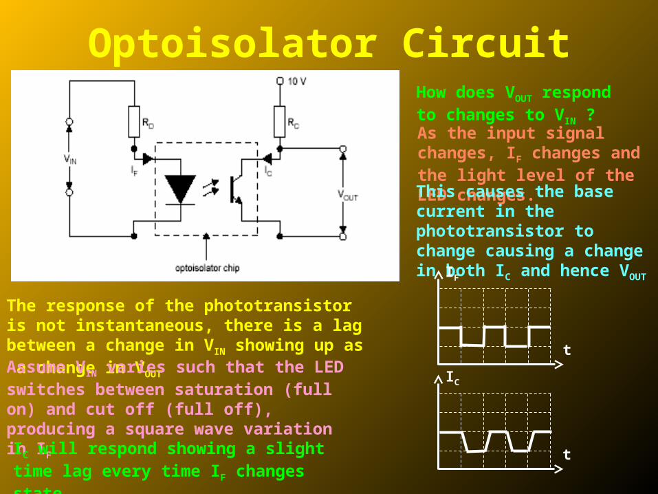
Optoisolator CircuitHow does VOUT respond to changes to VIN ? As the input signal changes, IF changes and the light level of the LED changes.This causes the base current in the phototransistor to change causing a change in both IC and hence VOUT
The response of the phototransistor is not instantaneous, there is a lag between a change in VIN showing up as a change in VOUT
IF
t
IC
t
Assume VIN varies such that the LED switches between saturation (full on) and cut off (full off), producing a square wave variation in IF
IC will respond showing a slight time lag every time IF changes state

Opto-electronic DevicesAn op amp (operational amplifier) is a high gain, linear, DC amplifierThe inputs marked as (+) and (-) do not refer to power supply connections but instead refer to inverting and non inverting capabilities of the amplifier.

The End