Embed Size (px)
Citation preview

Page 1
Verification of ZVS Boost Converter with Resonant circuit & Modelling of an Accurate Two-Diode PV Array System Simulator using MATLAB Simulink
ASHISH MEHER (110EE0206)
PRATEEK K LENKA (110EE0203)
MANISH BHAGAT (110EE0191)
Department of Electrical Engineering
National Institute of Technology, Rourkela
Page 2
END SEMESTER REPORT
Verification of ZVS Boost Converter with Resonant circuit & Modelling of an Accurate Two-Diode PV Array System Simulator
using MATLAB Simulink
A Thesis Submitted in Partial Fulfilment of the Requirements for the Degree of
Bachelor of Technology in “Electrical Engineering”
By:
ASHISH MEHER (110EE0206)
PRATEEK K LENKA (110EE0203)
MANISH BHAGAT (110EE0191)
Under the Supervision of
Prof. K. Ratna Subhashini
Department of Electrical Engineering
National Institute of Technology, Rourkela
Odisha, India-769008
May- 2014
Page 3
DEPARTMENT OF ELECTRICAL ENGINEERING NATIONAL INSTITUTE OF TECHNOLOGY
ROURKELA, ODISHA, INDIA-769008
CERTIFICATE
This is to certify that the thesis entitled “Verification of ZVS Boost Converter with Resonant circuit & Modelling of an Accurate Two-Diode PV Array System Simulator using MATLAB Simulink”, submitted by Ashish Meher(110EE0206), Prateek Kumar Lenka(110EE0203) & Manish Bhagat(110EE0191) in partial fulfilment of the requirements for the award of Bachelor of Technology in Electrical Engineering during session 2013-2014 at National Institute of Technology, Rourkela. A bonafide record of research work carried out by them under my supervision and guidance.
The candidates have fulfilled all the prescribed requirements.
The thesis which is based on candidates’ own work, have not submitted elsewhere for a degree/diploma.
In my opinion, the thesis is of standard required for the award of a bachelor of technology degree in Electrical Engineering.
Place: Rourkela K. Ratna Subhashini
Dept. of Electrical Engineering,
National institute of Technology,
Rourkela-769008, ODISHA.
Page 4
Electrical Engineering Department
National Institute Of Technology -Rourkela
ACKNOWLEDGEMENTS
We would like to express our sincere thanks to our project supervisor Prof. B. Chitti Babu, Department of Electrical Engineering, N.I.T. Rourkela, for his constant support, timely help, guidance & sincere co-operation during the entire period of our work. We are grateful to him for providing all the necessary facilities during the course of the project work.
We would also like to thank Prof. (Mrs.) K. Ratna Subhashini, Assistant Professor, NIT Rourkela, for the help provided during various stages of the project.
Finally, an honourable mention goes to our friends & families for their understanding and support in order to complete this project. Without the help of those mentioned above, this project could not have been completed.
Ashish Meher (110EE0206)
Prateek K. Lenka (110EE0203)
Manish Bhagat (110EE0191)
B.Tech (Electrical Engineering)

Page 5
Dedicated to
Our Parents
Page 6
ABSTRACT
This thesis proposes a MATLAB Simulink simulator for Photo Voltaic (PV) Array system. The main contribution is the utilisation of a Two-Diode model to represent a PV cell. This model is preferred because of its better accuracy at low irradiance levels. A PV of Kyocera (KC200GT) 50*10 Array is taken & the characteristics curves are plotted. The same simulator can be interfaced with MPPT algorithms & Power Electronics converters for better efficiency. The P-V & I-V Curves of this simulator is found in exact with that given by the manufacturers. It is expected that the proposed work can be very useful for PV professionals who require a simple, fast & accurate PV simulator in order to design their systems. A detailed analysis of a resonant circuit based soft-switching boost-converter for PV applications is also performed. The converter operates at Zero Voltage Switching (ZVS) turn-on and turn-off of the main switch, & Zero Current Switching (ZCS) turn-on and ZVS turn-off of the auxiliary switch due to resonant circuit incorporated into the circuit. Detailed operation of the converters, analysis of various modes, simulation as well as experimental results for the design has also been aptly presented. ZVS & ZCS technique is chosen; as it eliminates switching losses and noise due to discharging of junction capacitances. The systems are modelled & simulated in MATLAB 2013a 64-bit version and the output waveforms are shown.

Page 7
ABBREVIATIONS AND ACRONYMS
PV - Photo Voltaic
PVA - Photo Voltaic Array
SPV - Solar Photo Voltaic
ZVS - Zero Voltage Switching
ZCS - Zero Current Switching
MOSFET - Metal Oxide Semiconductor Field Effect Transistor
MATLAB - MATrix LABoratory
MPPT - Maximum Power Point Tracking
EMI - Electro Magnetic Interference
PWM - Pulse Width Modulation
Page 8
Table of Contents ACKNOWLEDGEMENTS ...................................................................................................................... 4
ABSTRACT ......................................................................................................................................... 6
ABBREVIATIONS AND ACRONYMS ..................................................................................................... 7
LIST OF FIGURES .............................................................................................................................. 10
LIST OF TABLES ................................................................................................................................ 10
Chapter 1 ........................................................................................................................................ 11
Introduction .................................................................................................................................... 11
1.1 Introduction: .......................................................................................................................... 12
1.2 Converter Topology Used For Pv Systems: ............................................................................. 13
1.3 Literature Survey: .................................................................................................................. 14
1.4 Motivation: ............................................................................................................................ 15
1.5 Thesis Objective: .................................................................................................................... 15
1.6 Thesis Outline: ....................................................................................................................... 15
1.7 Road Maps: ............................................................................................................................ 16
Chapter 2 ........................................................................................................................................ 17
Photovoltaic Systems ...................................................................................................................... 17
2.1 Photovoltaic Groupings: ......................................................................................................... 18
2.1.1 Photovoltaic cell: ............................................................................................................. 18
2.1.2 Photovoltaic module: ...................................................................................................... 19
2.1.3 Photovoltaic Array: ......................................................................................................... 19
2.2 Working of a PV cell: .............................................................................................................. 20
2.3 Characteristics of a PV cell (Two-Diode Model): ..................................................................... 20
Chapter 3 ........................................................................................................................................ 23
Modelling of PV array ...................................................................................................................... 23
3.1 Representation of PV devices: ................................................................................................ 24
3.1.1. Single diode model:........................................................................................................ 24
3.1.2. Two diode model: .......................................................................................................... 25
3.2 Improved Computational Method: .......................................................................................... 25
3.3 Determination of the 푹푺 & 푹푷 Values: .................................................................................. 26
3.4 Simulation Results: ................................................................................................................ 27

Page 9
Chapter 4 ........................................................................................................................................ 30
DC Chopper Circuits ......................................................................................................................... 30
4.1 Introduction: .......................................................................................................................... 31
4.2 Boost Converter: .................................................................................................................... 31
Chapter 5 ........................................................................................................................................ 33
Soft Switching of DC-DC
Boost Converter .............................................................................................................................. 33
5.1 Introductions: ........................................................................................................................ 34
5.2 Soft Switching In Boost Converters:........................................................................................ 34
5.3 Analysis of Various Operations Intervals:- .............................................................................. 35
A. Interval 1 (풕ퟎ − 풕ퟏ): ............................................................................................................. 35
B. Interval 2 (풕ퟏ − 풕ퟐ): ............................................................................................................. 36
C. Interval 3 (풕ퟐ − 풕ퟑ): ............................................................................................................. 36
D. Interval 4 (풕ퟑ − 풕ퟒ): ............................................................................................................ 37
E. Interval 5 (풕ퟒ − 풕ퟓ): ............................................................................................................. 37
F. Interval 6 (풕ퟓ − 풕ퟔ): ............................................................................................................. 38
G. Interval 7 (풕ퟔ − 풕ퟕ): ............................................................................................................ 38
H. Interval 8 (풕ퟕ − 풕ퟖ): ............................................................................................................ 39
I. Interval 9 (풕ퟖ − 풕ퟗ): .............................................................................................................. 39
5.4 Theory of Main & Auxiliary Switch:- ....................................................................................... 40
Chapter 6 ........................................................................................................................................ 41
Experimental Results
& Conclusions .................................................................................................................................. 41
6.1 PV Modelling Conclusions: ..................................................................................................... 42
6.2 Soft Switching Boost Converter Results: ................................................................................. 42
6.3 Simulation Results of Soft Switching Boost Converter: ........................................................... 43
6.4 Soft Switching Boost Converter Conclusions:.......................................................................... 45
BIBLIOGRAPHY: ............................................................................................................................... 46
Page 10
LIST OF FIGURES
Fig. 1: Basic PV cell structure 17
Fig. 2: Photovoltaic Hierarchy 18
Fig. 3: Characteristics of a PV cell 19
Fig. 4: Two diode model of PV cell 20
Fig. 5: Single diode model of PV cell 13
Fig. 6: PV simulator Block in Simulink 26
Fig. 7: Input parameter window of Kyocera (KG200GT) 50*10 Array 26
Fig. 8: Curves I-V of Kyocera @different Temp & @different Irradiation 27
Fig. 9: Curves P-V of Kyocera @different Temp & @different Irradiation 27
Fig. 10: Curves I-V & P-V of Kyocera for shading pattern 27
Fig. 11: Relative Error for 푉 & 푃 28
Fig. 12: Fly back mode boost converter 31
Fig. 13: Output Voltage waveforms of Boost Converter 31
Fig. 14: The topology for Soft-Switching Boost Converter 33
Fig. 15: Theoretical waveforms for Soft Switching Converter 34
Fig. 16: Soft Switching Boost Converter Simulink Circuit 43
Fig. 17: Various Simulation Result Waveforms 44
Fig. 18: Load Current & Voltage Waveforms 45
LIST OF TABLES
Table No. 1: ISTC Specifications for the 3 Modules used in experiments 28
Table No. 2: Parameters for Proposed Two-Diode Model 28
Table No. 3: Parameters used for the Simulation of Soft switching Boost converter 42

Page 11
Chapter 1
Introduction
Page 12
Chapter 1
1.1 Introduction: Most important worries in our power industry is the continuously
increasing power requirement but the unavailability of adequate resources to encounter its requirement by using the conventional sources of energy. Power demand has increased for the non-conventional sources of energies should be used along with the conventional systems to fulfil the energy demands. Non-conventional energy sources like solar energy and wind energy are the leading sources of energy; which are mainly used in this favour to extract green energy. The daily usage of fossil fuels has affected its deposit to be decreased drastically and has critically affected the environment, thus depleting the biosphere & resulting the global warming.
Solar energy is profusely obtainable on earth that has made it conceivable to harvest & utilize it suitably. Solar energy may be a grid connected generating unit or a standalone one depending on the availability of a grid nearby. As a result it can be implemented to power the rural areas; where the accessibility of grids is very less. Another advantage of using solar energy is the transportable operation wherever & whenever necessary.
Photovoltaic (PVs) are arrays/module (combination of smallest unit called cells) that contain a semiconductor material, which converts solar energy into electrical energy. PV systems include multiple components like mechanical and electrical connections and mountings and various means of regulating and (if required) modifying the electrical outputs. Materials which are used in photovoltaic applications are poly-crystalline silicon, mono-crystalline silicon, micro-crystalline silicon (amorphous) and cadmium telluride. The current and voltage that available at the PV device output terminals can be directly used to feed any small loads like lighting systems or small DC motors.
This PV array can also be interfaced with MPPT algorithm & power electronic converters to extract maximum power.
Due to the further development in the direction of power electronics, it has also been possible to further reduce the losses during switching in the converters, which are being used along with the PV array/module.

Page 13
1.2 Converter Topology Used For Pv Systems: In order to feed the power from non-conventional energy sources like photovoltaic array/module, DC-DC converters has played an important role during interfacing & to supply required AC or DC power. Hence for efficient load management it is necessary that the interfacing converter should be highly efficient. Here DC-DC Boost converter is taken, which is the most popular topology for obtaining the constant value of high DC output. Because of its simplicity which leads to high reliability & high efficiency at lower cost.
Due to overlapping of current & voltage waveforms, in case of the hard switching boost converters, during switching and the reverse recovery of the diode, there lies a high amount of switching loss with each of the switching cycle.
In order to eliminate the above shortcomings, new power electronics circuits are being based on resonant and soft-switching technologies. Hence an increase in the efficiency of the system is obtained as to the non-overlapping of the voltage and current waveforms during switching. This results in the decrease in output ripples at higher values of frequencies. Also, it is possible to use smaller values of inductors and capacitors, with the increase in frequencies, which results in the reduction of the components sizes and thus increasing the power density.
This thesis highlights on a soft switching technique which provides ZVS turn-on and turn-off for the main switch & ZCS turn-on and ZVS turn-off with the use of resonant circuit by the auxiliary switch. An anti-parallel diode is added across the main switch in order to make the voltage zero across it before current starts to builds, thus making ZVS turn-on process and a capacitor is connected across it to reduce the rate of rise of voltage across the main switch, thus making ZVS turn-off process. The auxiliary switch operates with ZCS using the resonance circuit. This soft switching method is selected over other methods used for soft-switching because the resonant circuit implemented for this performs dual operation. It not only makes ZVS turn-off of the main switch and auxiliary switch but also ensures the ZCS turn-on of the auxiliary switch. Hence, along with the conduction losses of the auxiliary switch, the switching losses are also drastically decreased.
Page 14
1.3 Literature Survey: The utilization of solar energy has been looked upon by many scientists
all around the world. It has been known that solar cell operates at very less efficiency (up to 19% max.) and thus there is a need of best control mechanism to increase the efficiency of the solar cell. In this area researchers have developed what are now called as the Maximum Power Point Tracking (MPPT) algorithms.
Mummadi Veerachary has given a detailed report on the use of a SEPIC converter in the area of photovoltaic power control. In his thesis he used a two-input converter for accomplishing the maximum power extraction from the solar cell.
M. G. Villalva in his both reports has presented a comprehensive method to model a solar cell using Simulink. His results were quite similar to the characteristics of the solar cell output plots.
P. S. Revankar has even included the variation of sun’s inclination to track down the maximum possible power from the incoming solar radiations. The control mechanism changes the position of the panel such that the incoming solar radiations are always perpendicular to it.
M. Berrera has compared seven different algorithms for maximum power point tracking using two different solar irradiation functions to depict the variation of the output power in both cases using the MPPT algorithms and optimized MPPT algorithms.
Ramos Hernanz has also successfully presented the modelling of a solar cell and the variation of the current-voltage curve and the power-voltage curve due the solar irradiation changes and the change in ambient temperature.
Soft-switching technique was developed in the middle of 1980s. Power electronic engineers who were familiar with phase-controlled thyristor converters already know that switching loss in this class of converters is much less or negligible, thus contributes to the high conversion efficiency.

Page 15
1.4 Motivation: Photovoltaic power control is one of the burning research fields
these days. Researchers are round the clock to develop better solar cell materials and efficient control mechanisms. The challenge of the project and the new area of study were the motivations behind the project. In India, there are nearly 300 sunny days in a year & abundant solar energy is available in nearly most parts of the country, both in the urban/rural areas.
But still we have lots of distance to cover, in order to effectively utilise the solar power. In contrast to fossil fuels, it became a cheap and effective solution for both commercial & domestic use. With the day-by-day increasing demand for the renewable energy sources, the productivity of photovoltaic modules/ array has advanced dramatically in recent years. Its efficient usage has led to increasing the role of photovoltaic technology as reliable and robust means of harnessing renewable energy.
1.5 Thesis Objective: The following objectives are being achieved at the completion of the project:
1) To design an exact Two-diode Photovoltaic Array system simulator using the Simulink models; which will be more user-friendly & to observe its characteristics.
2) To design & analyse the operation of Boost converter. 3) To study the soft-switching technique of DC-DC Boost converter &
detailed analysis of its operations.
1.6 Thesis Outline: The thesis has been broadly divided into 6 chapters. The first chapter
includes the introduction, converter topology, literature survey, motivation, objectives & road-maps. Chapter 2 is based on PV characteristic. Chapter 3 deals with the modelling of PV Array. Chapter 4 consists of chopper circuit & hardware verification of Boost converter. Chapter 5 deals with the soft switching techniques & various modes of operation. Chapter 6 shows the results of the Simulink model & the conclusions drawn.
Page 16
1.7 Road Maps:
The project has been started from the month of January 2014, when the results of PV array (i.e. the accurate P-V & I-V Characteristics) were obtained. In the same month the accuracy was checked by applying the same model to five PV modules of different kind. In February the results were verified under Partial Shadings conditions & hardware implementation of Boost converter was done. In subsequent months the MATLAB model of the boost converter along with ZVS switching method being simulated & the results were obtained.
Page 17
Chapter 2
Photovoltaic Systems

Page 18
Chapter 2
The effect of the photoelectric was first founded by a French physicist, Edmund Bequerel in back 1839. He noted that certain materials have property to produce small amounts of electric current when exposed to the sunlight. In 1905, Albert Einstein demonstrated the nature of light & the photoelectric effect which has become the basic principle for photovoltaic technology. The first photovoltaic module was built by Bell Laboratories in back 1954.
2.1 Photovoltaic Groupings: PV system consists of 3 types of groups; namely:
2.1.1 Photovoltaic cell
2.1.2 Photovoltaic module
2.1.3 Photovoltaic Array
2.1.1 Photovoltaic cell: PV cells are basically a diode made of semiconductor materials. Like a
diode, this PV cells also has a p-n junction & produces electricity when directly exposed to sun-light. PV cell are basically made up of various types of semi-conductor materials like mono-crystalline, poly-crystalline, amorphous & thin film. Mono-crystalline and Poly-crystalline silicon are widely used for the commercial use because of high efficiency.
Fig. 1 – PV Basic cell structure

Page 19
2.1.2 Photovoltaic module: A single PV cell is incapable to produce the power for general purpose.
Therefore by inter-connecting several PV cell in parallel (for high current requirements) & in series (for high voltage requirements) can fetch us the required power. Normally a series connection is chosen, which is mainly recognized as a module. A module normally comprise of 36 or 72 cells. The modules consist of a transparent front side & an encapsulated PV cell at the back side. The front side materials are usually made up from low-iron and tempered glass. The overall efficiency of a PV module is less than that of a PV cell. This is due to the fact that some radiations are reflected by the glass surface cover, thus by reducing the overall efficiency of the module.
2.1.3 Photovoltaic Array: Photo-voltaic array is made by inter-connecting many modules in series
& parallel manner to meet the power requirement. The energy generated by a single module is hardly enough to use for commercial purpose. So modules are linked in many ways; like Series-Parallel, Bridge-Linked & Totally Crossed Tied; to supply the load with at most efficiency. In metropolitan areas, normally the arrays are attached on the roofs. Also for the agricultural purpose, the array output can be directly supplied to a DC motor.
Fig. 2 - Hierarchy of Photovoltaic

Page 20
2.2 Working of a PV cell: Photoelectric effect is the elementary principle of working of a PV cell. It
can be described as the phenomenon in which a semi-conductor diode absorbs a certain wavelength of sun light mainly of UV/Infrared/visible regions & ejects an electron. When the sunbeam falls on PV cell surface, some part of the solar energy are being scattered & reflected, while others are absorbed by this material. If the absorbed solar energy is much greater than the band gap energy of the semi-conductor material, then an electron migrates from valence band into the conduction band. By this process, lots of hole-electron pairs are generated inside the semiconductor. The electrons formed by this process are much mobile to move by the action of small electric potential. These free electrons are enforced to move in a particular direction by the action of electric field created in the PV cells. These free electrons thus forms current and that can be drained out for peripheral use by attaching a metal plate on the top and the bottom of PV cell. This current and the voltage are basically responsible for the necessary output power.
2.3 Characteristics of a PV cell (Two-Diode Model): PV characteristic consists of mainly three important points namely; Open
circuit voltage (Voc), short circuit current (Isc) and Maximum power point (Impp, Vmpp, Pmpp) i.e. the maximum powers that can be extracted from a PV cell are at the maximum power point. Usually manufacturers provide these parameters in their datasheets for a particular PV cell or module at a particular temperature & irradiance (i.e. @STP- 25°C & 1000w/m²). By using these parameters we can construct a simple model but for designing an accurate model more information are needed.
Fig. 3 -PV cell Characteristics
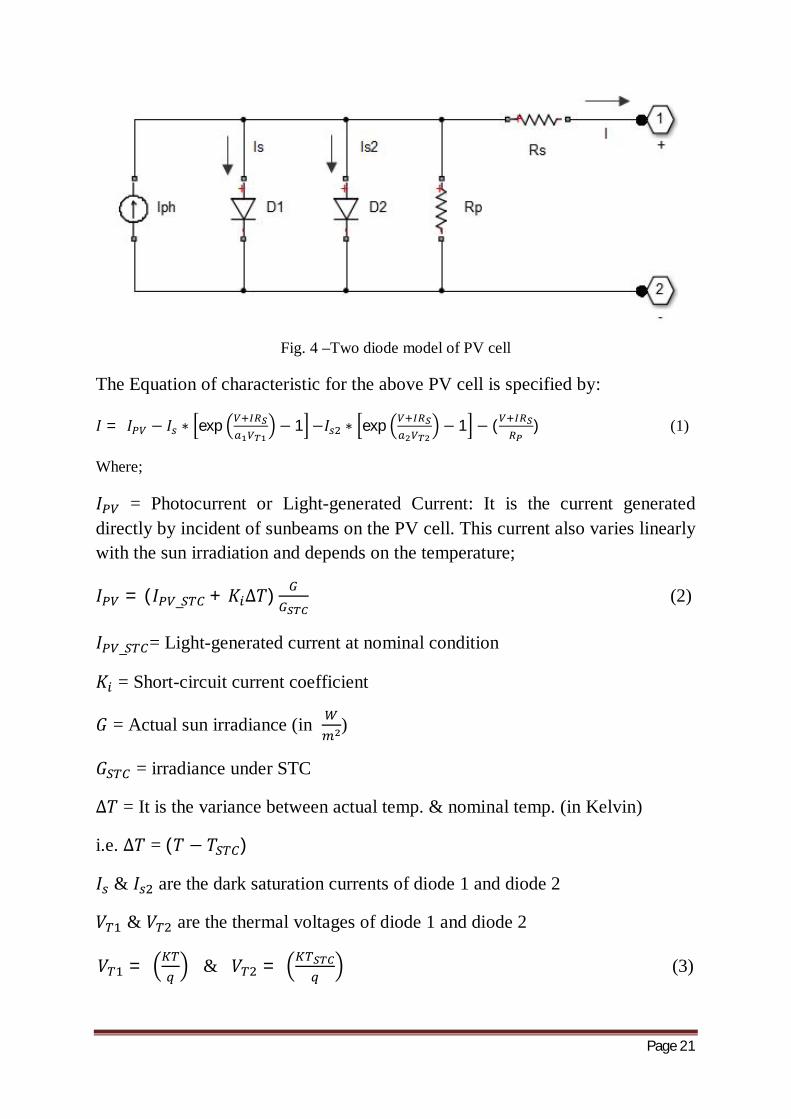
Page 21
Fig. 4 –Two diode model of PV cell
The Equation of characteristic for the above PV cell is specified by:
퐼 = 퐼 − 퐼 ∗ exp − 1 −퐼 ∗ exp − 1 − ( ) (1)
Where;
퐼 = Photocurrent or Light-generated Current: It is the current generated directly by incident of sunbeams on the PV cell. This current also varies linearly with the sun irradiation and depends on the temperature;
퐼 = (퐼 _ + 퐾 ∆푇) (2)
퐼 _ = Light-generated current at nominal condition
퐾 = Short-circuit current coefficient
퐺 = Actual sun irradiance (in )
퐺 = irradiance under STC
∆푇 = It is the variance between actual temp. & nominal temp. (in Kelvin)
i.e. ∆푇 = (푇 − 푇 )
퐼 & 퐼 are the dark saturation currents of diode 1 and diode 2
푉 & 푉 are the thermal voltages of diode 1 and diode 2
푉 = & 푉 = (3)
Page 22
Where,
K= Boltzmann constant = 1.3806503 × 10 J/K
q = electron charge = 1.607 × 10 C
T = Nominal Temperature = 298.15 K
푎 & 푎 represent the diode ideal constants
푅 & 푅 = Due to the presence of internal resistances, (like contact resistances & manufacturing defects) the power loss takes place in the cell. These internal resistances can be isolated into series resistance,푅 and parallel resistance, 푅 . For the ideal case, 푅 would be “zero” & 푅 would be “infinity”.
Under STC: 퐺 = 1000 & 푇 = 25° 퐶 (4)
Page 23
Chapter 3
Modelling of PV array

Page 24
Chapter 3
3.1 Representation of PV devices: In this chapter, we will enlighten the basic models of PV array and their advantages and disadvantages over each other’s. Then, we will go through a new method to extract the unknown parameters using known ones.
The PV devices are essentially represented in two different models viz.
3.1.1. Single diode model
3.1.2. Double diode model
3.1.1. Single diode model: In a single diode model, there is a current source in parallel to a diode. The current source signifies the light-generated current, 퐼 that varies linearly with the solar irradiation. This is the simplest and most widely used model for simulations as it offers a good compromise between simplicity, reliability and accuracy. Figure below indicates the single diode model circuit.
Fig. 5 –Single diode model of PV cell
Disadvantages:
The single diode models were based on the postulation that the recombination losses are absent in the depletion region. But, in a real solar cell, the recombination loss represents a significant loss, especially at low voltages. Whereas in two-diode model the insertion of an additional diode increases the preciseness.

Page 25
3.1.2. Two diode model: In this model an additional diode is attached in parallel to the single diode model circuit. This diode is incorporated to provide an even more accurate & precise I-V characteristic curve that also deliberates for the difference in flow of current at low current values due to charge recombination in the depletion region of the semi-conductor. (Two diode model figure No. 2)
The characteristic equation for PV cell is given by:
퐼 = 퐼 − 퐼 ∗ exp − 1 −퐼 ∗ exp − 1 − ( ) (5)
(Note: All the parameters are explained in previous chapter)
The 퐼 term in the above equation, recompenses the recombination loss in the depletion region.
Although greater accurateness can be achieved by using this model; but it requires the working out of seven parameters, namely 퐼 , 퐼 , 퐼 , 푎 , 푎 ,푅 & 푅 .
To shorten the calculation we have assumed 푎 = 1 & 푎 = 2. These values are guesstimate of the Schokley-Read-Hall recombination in space charge layer.
3.2 Improved Computational Method: To further simplify, both the 퐼 & 퐼 are set to be equal in magnitude:
퐼 = 퐼 = ( _ ∆ )_ ∆
( )/ ∗
(6)
퐾 = the open-circuit voltage coefficient (presented from data-sheets)
The equalisation shortens the computation as no iteration is required.
According to the Shockley’s Diffusion Theory;
푎 Must be unity & (푎 + 푎 )/푝 = 1 (7)
Page 26
Hence the above equation again simplifies to:
퐼 = 퐼 = ( _ ∆ )_ ∆ (8)
Up to this five parameters of this model are easily calculated, i.e. 퐼 , 푎 , 푎 , 퐼 , 퐼 & the values of 푅 , 푅 are achieved through iteration.
3.3 Determination of the 푹푺 & 푹푷 Values: The residual two parameters 푅 & 푅 are attained through successive iteration. The idea is to maximize the power point (푃 ) matching; i.e. to match the calculated peak power (푃 , ) & the experimental/ manufacturer peak power (푃 , ) by iteratively increasing the value of 푅 while concurrently manipulating the value of 푅 .
Under maximum power-point condition, 푅 can be written as
푅 = ( )[ , ]
(9)
Where, 퐼 = 퐼 [exp − 1] (10)
퐼 = 퐼 [exp푉 + 퐼 푅
푎 푉− 1]
The initial circumstances for both resistances are given below:
푅 = 0 & 푅 = − (11)

Page 27
3.4 Simulation Results:
Fig. 6 –PV simulator Block in Simulink
Fig. 7 –Input parameter window of Kyocera (KG200GT) 50*10 Array
Page 28
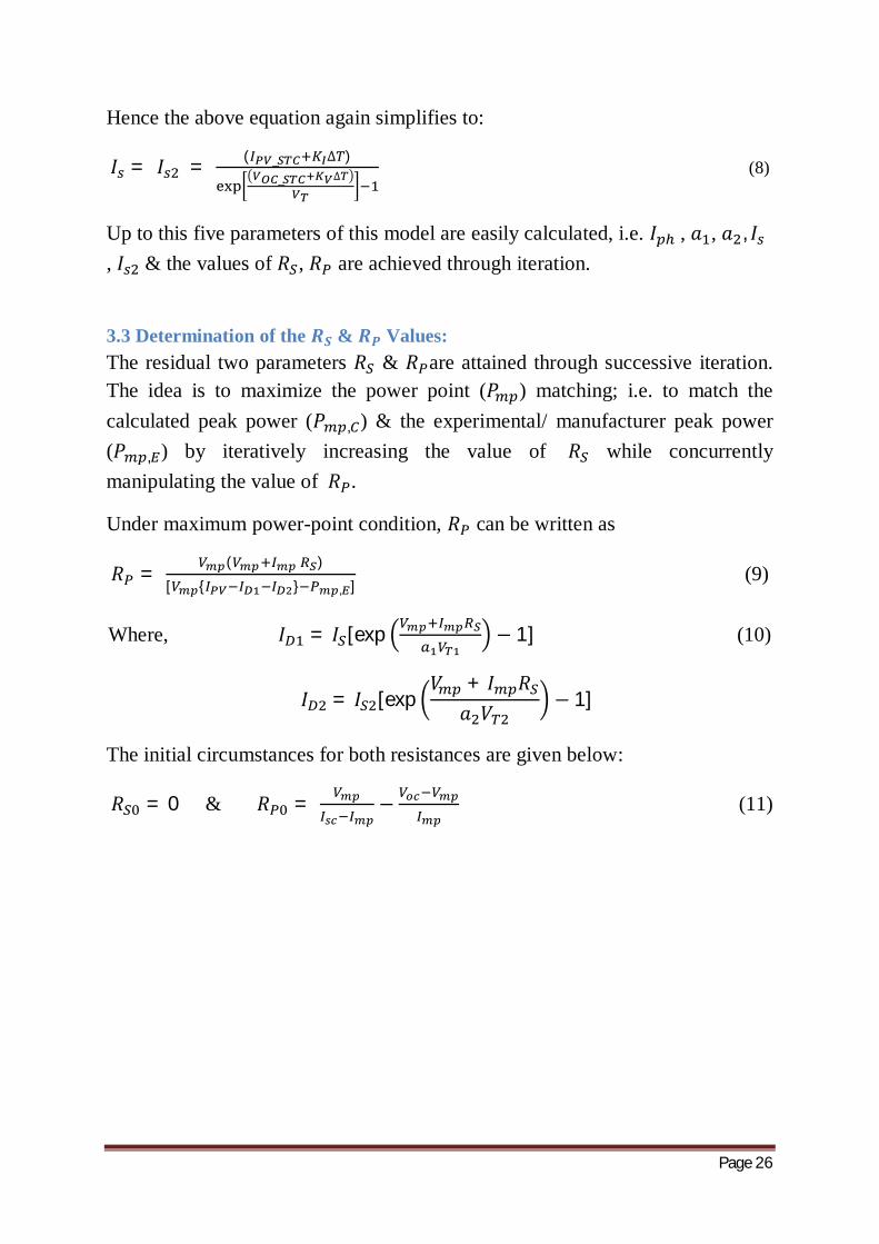
Fig. 8 – Curves I-V of Kyocera @different Temp & @different Irradiation
Fig. 9 – Curves P-V of Kyocera @different Temp & @different Irradiation
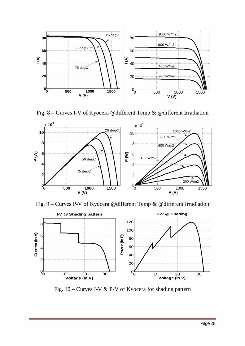
Fig. 10 – Curves I-V & P-V of Kyocera for shading pattern
0 500 1000 15000
20
40
60
80
V (V)
I (A
)25 degC
50 degC
75 degC
0 500 1000 15000
20
40
60
80
V (V)
I (A
)
1000 W/m2
400 W/m2
200 W/m2
800 W/m2
0 500 1000 15000
2
4
6
8
10
x 104
V (V)
P (W
)
50 degC
75 degC
25 degC
0 500 1000 15000
2
4
6
8
10
x 104
V (V)
P (W
)1000 W/m2
800 W/m2
600 W/m2
400 W/m2
200 W/m2
0 10 20 300
2
4
6
8
I-V @ Shading pattern
Voltage (in V)
Cur
rent
(in
A)
0 10 20 300
20
40
60
80
100
120
P-V @ Shading
Voltage (in V)
Pow
er (i
n P)
Page 29
Sl.No
Parameter
Multi-crystalline Mono-crystalline
SP-70
Thin-Film
ST-40 BP Solar MSX-60
Kyocera KG200GT
Shell S36
01 퐼 3.8 A 8.21 A 2.3 A 4.7 A 2.68 A 02 푉 21.1 V 32.9 V 21.4 V 21.4 V 23.3 V 03 퐼 3.5 A 7.61 A 2.18 A 4.25 A 2.41 A 04 푉 17.1 V 26.3 V 16.5 V 16.5 V 16.6 V 05 퐾 -80 mV/°C -123 mV/°C -76 mV/°C -76 mV/°C -100mV/°C
06 퐾 3 mA/°C 3.18 mA/°C 1 mA/°C 2 mA/°C 0.35 mA/°C
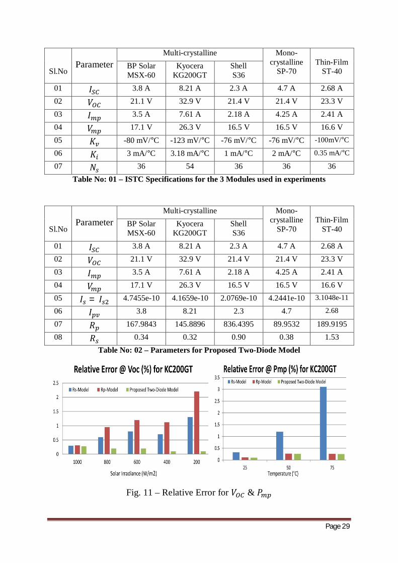
07 푁 36 54 36 36 36 Table No: 01 – ISTC Specifications for the 3 Modules used in experiments
Sl.No
Parameter
Multi-crystalline Mono-crystalline
SP-70
Thin-Film
ST-40 BP Solar MSX-60
Kyocera KG200GT
Shell S36
01 퐼 3.8 A 8.21 A 2.3 A 4.7 A 2.68 A 02 푉 21.1 V 32.9 V 21.4 V 21.4 V 23.3 V 03 퐼 3.5 A 7.61 A 2.18 A 4.25 A 2.41 A 04 푉 17.1 V 26.3 V 16.5 V 16.5 V 16.6 V 05 퐼 = 퐼 4.7455e-10 4.1659e-10 2.0769e-10 4.2441e-10 3.1048e-11
06 퐼 3.8 8.21 2.3 4.7 2.68
07 푅 167.9843 145.8896 836.4395 89.9532 189.9195 08 푅 0.34 0.32 0.90 0.38 1.53
Table No: 02 – Parameters for Proposed Two-Diode Model
Fig. 11 – Relative Error for 푉 & 푃

Page 30
Chapter 4
DC Chopper Circuits
Page 31
Chapter 4
4.1 Introduction: Now-a-days DC power sources are widely used many industrial applications. Variable DC voltage sources however, perform better in order to extract power at maximum efficiency. Examples of such DC system are subway cars, battery-operated vehicles, trolley buses, battery charging etc.
A chopper is a static device that transforms directly a fixed dc voltage to an adjustable dc output voltage. A chopper can also be assumed of as dc-equivalent of an AC transformer as they act in the same identical manner. Since a chopper comprises one stage transformation, these are more effective.
The power semiconductor devices which is used for the chopper circuit can be thyristor, power MOSFET, power BJT, GTO or IGBT. Like transformer, a chopper circuit can also be used to step-up or step-down the stationary input voltage.
Here, the Boost converter topology is used for obtaining a constant value of high DC output voltage.
4.2 Boost Converter: A boost converter (step-up converter) is a DC-to-DC power
converter with an output voltage greater than its input voltage. It is a part of switched-mode power supply (SMPS) containing at least two semiconductor switches (a diode and a transistor) and at least one energy storage constituent, a capacitor/ an inductor, or the two in combinations. Filters prepared of capacitors (occasionally in blend with inductors) are usually added to the output of the converter to shrink output voltage ripples.
There are two modes of action namely;
Continuous Mode: When a boost converter works in this mode, the current through the inductor never decreases to zero.
Discontinuous Mode: If the ripple amplitude of the current is too high, the inductor may be entirely discharged before the completion of the entire commutation cycle. This is commonly occur under light loads conditions. In this case, the current through the inductor falls to zero during part of the operation.
Page 32
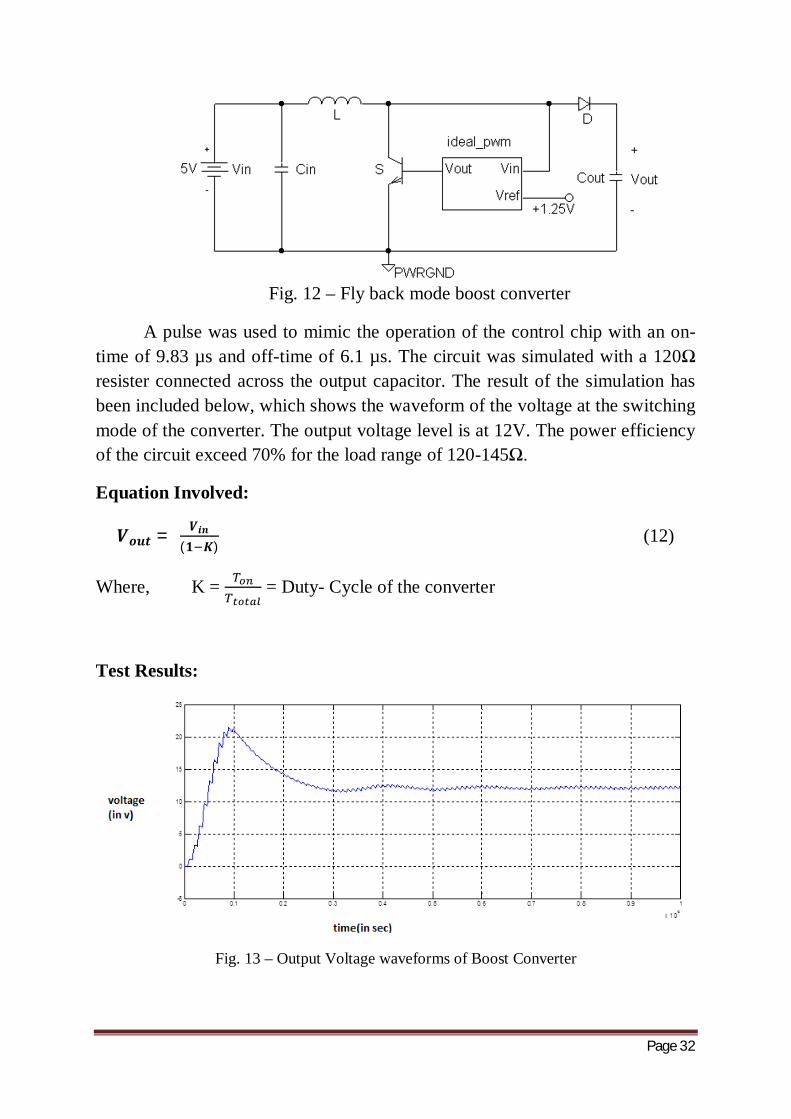
Fig. 12 – Fly back mode boost converter
A pulse was used to mimic the operation of the control chip with an on-time of 9.83 µs and off-time of 6.1 µs. The circuit was simulated with a 120Ω resister connected across the output capacitor. The result of the simulation has been included below, which shows the waveform of the voltage at the switching mode of the converter. The output voltage level is at 12V. The power efficiency of the circuit exceed 70% for the load range of 120-145Ω.
Equation Involved:
푽풐풖풕 = 푽풊풏(ퟏ 푲)
(12)
Where, K = = Duty- Cycle of the converter
Test Results:
Fig. 13 – Output Voltage waveforms of Boost Converter

Page 33
Chapter 5
Soft Switching of DC-DC
Boost Converter

Page 34
5.1 Introductions: Converters which use the conventional way of switching phenomenon are known as Hard Switching converters. When the switch is turn-on, the voltage across the switch tends to decrease while the current increases; which results in considerable switching losses.
Soft switching technique can be incorporated to reduce EMI, switching & conduction losses and switching stresses. If the semiconductor device is prepared to turn off or turn on when current or voltage is zero, then the product of voltage and current during transition period is zero which results to the zero power loss.
5.2 Soft Switching In Boost Converters: PV array can be interfaced with DC-DC Boost converter with soft
switching technique & MPPT tracker to extract maximum efficient power.
Fig. 14 – The topology for Soft-Switching Boost Converter

Page 35
The following assumptions are considered for the operation & analysis of the circuit:
Large input inductor to make the input current constant Large output capacitor to make output voltage constant
Fig. 15 – Theoretical waveforms for Soft Switching Converter
5.3 Analysis of Various Operations Intervals:-
A. Interval 1 (풕ퟎ − 풕ퟏ): In the commencement of this interval, the auxiliary switch 푺풂 is turned on
with ZCS process while the main switch remains off. A resonant loop consisting of 푳풎- 푳풓- 푪풓- 푺풂- 푽풊풏is formed because of the resonance between 푳풓 and 푪풓. The current in 푫풐풖풕 reaches zero (soft turn-off) at the end of the period. Now, when the current through 푳풎becomes equals to the current through 푳풓, mode 1 ends.
Page 36
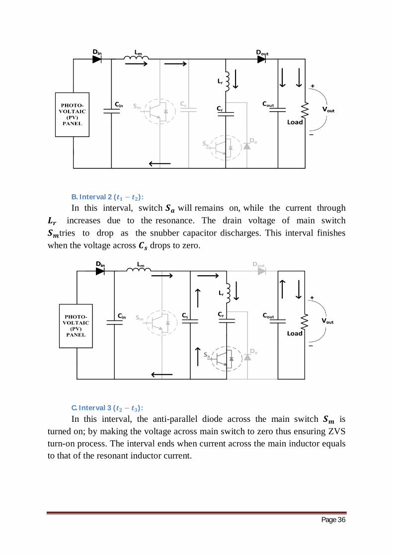
B. Interval 2 (풕ퟏ − 풕ퟐ): In this interval, switch 푺풂 will remains on, while the current through
푳풓 increases due to the resonance. The drain voltage of main switch 푺풎tries to drop as the snubber capacitor discharges. This interval finishes when the voltage across 푪풔 drops to zero.
C. Interval 3 (풕ퟐ − 풕ퟑ): In this interval, the anti-parallel diode across the main switch 푺풎 is turned on; by making the voltage across main switch to zero thus ensuring ZVS turn-on process. The interval ends when current across the main inductor equals to that of the resonant inductor current.

Page 37
D. Interval 4 (풕ퟑ − 풕ퟒ): In this interval, the main switch 푺풎 is being turned on at zero voltage
condition and henceforth, there are no switching losses through it. The resonant capacitor 푪풓 is charged uninterruptedly in this interval. The load current is constantly provided by the output capacitor.
E. Interval 5 (풕ퟒ − 풕ퟓ): In this mode, the current drifts through the anti-parallel diode of 푺풂. Hence, the switch 푺풂 is turned off certifying ZVS process. Thus, there is no switching loss in 푺풂 during the turn-off period. This period finishes when resonant capacitor 푪풓 is being fully charged.

Page 38
F. Interval 6 (풕ퟓ − 풕ퟔ): In this interval, the current drifts through the auxiliary diode 푫풂instead of
anti-parallel diode of switch 푺풂 . This interval split ends, when the main switch 푺풎 is turned off.
G. Interval 7 (풕ퟔ − 풕ퟕ): In this interval, the main switch 푺풎 is turned-off by ZVS process
under the assistance of snubber capacitor 푪풔 . During this time energy is being stored in the capacitor 푪풔 . This interval finishes when 푪풔 is charged fully.
Page 39
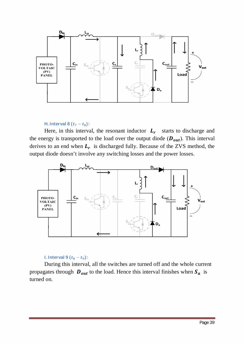
H. Interval 8 (풕ퟕ − 풕ퟖ): Here, in this interval, the resonant inductor 푳풓 starts to discharge and the energy is transported to the load over the output diode (푫풐풖풕). This interval derives to an end when 푳풓 is discharged fully. Because of the ZVS method, the output diode doesn’t involve any switching losses and the power losses.
I. Interval 9 (풕ퟖ − 풕ퟗ): During this interval, all the switches are turned off and the whole current propagates through 푫풐풖풕 to the load. Hence this interval finishes when 푺풂 is turned on.

Page 40
5.4 Theory of Main & Auxiliary Switch:- The duty-cycle of auxiliary switch is such that it forces the main switch to activate with soft switching. When the auxiliary switch is made turn-on then it forms a resonant loop between 푳풓 & 푪풓. ZVS process is mainly initiated during turning on of the auxiliary switch. The PWM pulses of the main switch have to make a delay than that of auxiliary switch. Soft switching with resonance is achieved by properly turning on the switches. During the suspension time auxiliary switch must remain turn on.
The least delay time must be fulfilled by the subsequent equation:
푇 ≥ + √(퐿 퐶 ) (13)
The voltage conversion equation is defined as:
≈ ( )
(14)
where,
퐷 = Duty cycle of the main switch
퐷 = Duty cycle of the auxiliary switch

Page 41
Chapter 6
Experimental Results
& Conclusions

Page 42
6.1 PV Modelling Conclusions: After going through the three arrays (i.e. Multi-crystalline, Mono-
crystalline & Thin-Film) used in the above experiment, we are concluded, regarding the effect of temperature & irradiance, that temperature mainly affects the voltage whereas irradiance affects the current across PV Module.
It was observed from the P-V or I-V curves of
Figure-8(i) that open-circuit voltage drops with the rise in temperature. Figure-8(ii) that short-circuits current drops with reduction in irradiation
which is understandable since, they retain a linear relationship. Figure-9(i) that with the rise in temperature the maximum power-point
drops. Figure-9(ii) that with the reduction in irradiation also the maximum
power-point decreases.
It has also been observed (from Fig. 11) that, under the STC (Standard Testing Conditions) irradiance level, there is a very slight difference in the 푉 values among the three models. When irradiance is reduced then substantial abnormality is witnessed with 푅 & 푅 models; similarly for 푃 .
Hence, from the above comparisons & simulation results it was concluded that the Proposed Two-Diode Model perfectly calculates 푃 under all conditions. This simulator can also be interfaced with MPPT algorithm & power electronic converters to extract maximum power.
6.2 Soft Switching Boost Converter Results: The following table shows all the parameters used during the simulation
& designing. The simulation is executed under resonant switching frequency (i.e. 160 KHz) & a rated power of 230W.
PV Array has an output voltage of 18V. A 10Ω load is attached across the output of the soft switching Boost converter.

Page 43
Parameters Label Value Output Voltage 푉 48.8 V
Rated Power 푃 230 W Main Inductor L 200 uH
Resonant Inductor 퐿 10 uH Resonant Capacitor 퐶 100 nF
Snubber Capacitance 퐶 0.3 uF Switching Frequency 푓 160 KHz
Input Capacitor 퐶 50 uF Output Capacitor 퐶 470 uF
Table No: 03 – Parameters used for the Simulation of Soft switching Boost converter
As we know that, resonance is formed between an inductor (퐿 ) & a capacitor (퐶 ) if the switching is done at resonance frequency (푓 ).
휔 = 2휋푓 = = 10 (15)
From the above equation, switching frequency (푓 = 푓 ) is obtained as 160KHz.
6.3 Simulation Results of Soft Switching Boost Converter: The MATLAB simulated soft switching Boost converter circuit is presented below.
Fig. 16 – Soft Switching Boost Converter Simulink Circuit
Page 44
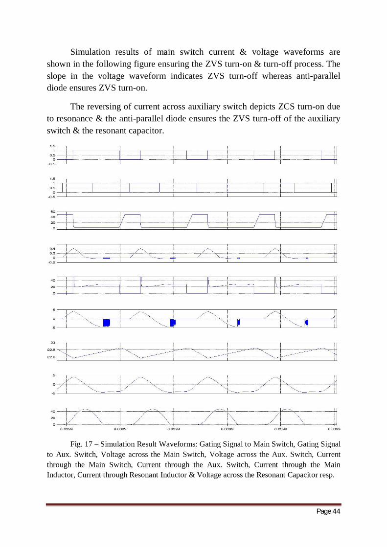
Simulation results of main switch current & voltage waveforms are shown in the following figure ensuring the ZVS turn-on & turn-off process. The slope in the voltage waveform indicates ZVS turn-off whereas anti-parallel diode ensures ZVS turn-on.
The reversing of current across auxiliary switch depicts ZCS turn-on due to resonance & the anti-parallel diode ensures the ZVS turn-off of the auxiliary switch & the resonant capacitor.
Fig. 17 – Simulation Result Waveforms: Gating Signal to Main Switch, Gating Signal to Aux. Switch, Voltage across the Main Switch, Voltage across the Aux. Switch, Current through the Main Switch, Current through the Aux. Switch, Current through the Main Inductor, Current through Resonant Inductor & Voltage across the Resonant Capacitor resp.

Page 45
The output current (퐼 ) & output voltage (푉 ) waveforms across the 10Ω load are also obtained & shown below:
Fig. 18 – Load Current & Voltage Waveforms
6.4 Soft Switching Boost Converter Conclusions:
An auxiliary resonant circuit ensuring Soft switching Boost converter along with the two diode equivalent model of PV Array has been discussed in this thesis. The simulation results ensure the soft switching of both the switches, thus eliminating switching losses, conduction losses, electric stresses & EMI. Proper design of inductor must be taken for appropriate soft switching as the inductor plays a very vital role in the design of Boost converter. A proper difference can be perceived in the effectiveness of Hard Switching & Soft Switching converters. This method of soft switching can be used for low power DC equipment mainly in telecom services. This soft switching method not only eliminates the losses but also increase the overall efficiency of PV systems thus making the overall system to cost-effective & reliable to use.

Page 46
BIBLIOGRAPHY:
[1] IEEE Standard Definitions of Terms for Solar Cells, 1969
[2] Gwinyai Dzimano, B.S. “Modeling of Photovoltaic Systems”, The Ohio State University, Pg.1-18,48-52, 2008.
[3] Ryan C. Campbell, A Circuit-based Photovoltaic Array Model for Power System Studies, Pg.1 Student Member, IEEE.
[4] H. J. M¨oller, Semiconductors for Solar Cells. Norwood, MA: Artech House, 1993.
[5] W. Xiao, W. G. Dunford, and A. Capel, “A novel modeling method for photovoltaic cells,” in Proc. IEEE 35th Annu. Power Electron. Spec. Conf. (PESC), 2004, vol. 3, pp. 1950–1956.
[6] N. Jain,”A Zero Voltage Switching Boost Converter using a Soft Switching Auxiliary Circuit with reduced conduction losses”, M.S.Thesis, Concordia University, Montreal, Canada. December 2000.
[7] G. Walker, “Evaluating MPPT converter topologies using a matlab PV model,” J. Elect. Electron. Eng., Australia, vol. 21, no. 1, pp. 45–55, 2001.
[8] Marcelo Gradella Villalva, Jonas Rafael Gazoli and Ernesto Ruppert Filho “Comprehensive Approach to Modeling and Simulation of Photovoltaic Arrays”, IEEE Transaction on Power Electronics, Vol. 24, No. 5, Pg.1198-1204, May 2009.
[9] A.S. Sedra & K.C. Smith, Microelectronic Circuits. London, U.K. Oxford Univ. Press, 2006.
[10] Daniel S.H. Chan, member IEEE and Jacob C.H. Phang, member IEEE, “Analytical Methods for the Extraction of Solar-Cell Single- and Double-Diode Model Parameters from I- V Characteristics”,IEEE transactions on electron devices, Vol.ED-34 No.2 February 1987.
[11] R. Gurunathan and A. K. S. Bhat, “A zero-voltage transition boost converter using a zero-voltage switching auxiliary circuit,” IEEE Trans. on Power Electronics, vol. 17, no. 5, pp. 658-668, September 2002.
[12] S.H. Park, G.R. Cha, Y.C. Jung and C.Y. Won, “Design and application for PV generation system using a soft switching boost converter with SARC,” IEEE Trans. on Industrial Electronics, vol. 57, no. 2, pp515-522, February (2010).
![Voltage mode control of soft-switched single switch ... · achieving ZVS and ZCS [28]. Quasi resonant converters [29] employ a single switch and provide soft switching condition without](https://img.pdfslide.net/doc/110x75/5e31277ee80634229e625f9c/voltage-mode-control-of-soft-switched-single-switch-achieving-zvs-and-zcs-28.jpg)


![Survey stability of the ZVS phase-shifted full-bridge DC ...journal.it.cas.cz/62(2017)-KHO/Paper Sharif260.pdf · ZVS PWM in [4] is formed by a diode, a resonant capacitor and a resistor](https://img.pdfslide.net/doc/110x75/5e3125c4d23e5149907b5255/survey-stability-of-the-zvs-phase-shifted-full-bridge-dc-2017-khopaper-sharif260pdf.jpg)