Embed Size (px)
Citation preview

Vertex Summary at LCWS2007
Summary Report on VTX R&D
SLAC CERNDESY
KEK
Hwanbae Park (Kyungpook Nat’l Univ.)
- close to IP : reduce extrapolation error - impact parameter resolution: ≤ 5µm 10µm/(p sin3/2 ) - minimal multiple scattering : < 0.1% X0/layer - occupancy small pixel size data sparsification and zero suppression
requires silicon sensors which are substantially thinner and more precise than LHC
motivates new directions for R&D on silicon sensors:
Test Facilities (4 talks) Sensor Technology (6 talks) Background Simulation (2 talks) Integration (3 talks)
outlook
Vertex Summary@DESY, LCWS2007
Progress on Test Facilities - SLAC, LBNL, DESY, CERN, FNAL

Vertex Summary@DESY, LCWS2007
Test Facilities: EMI Studies at SLAC ESA (by M. Woods)
VXD phase-lock loop monitor
Bicon antenna (50mV/div)
YAGI antenna (5mV/div)
40ns/divBeam Trigger
EMI from gaps (toroids, …) downstream
no failures
Placing just the VXD board inside an aluminum foil shielded box, covering the gap stopped failures- failures not due to ground loops or EMI on power/signal cables - failures are due to EMI emitted by gap which are camera windows, BPM feedthroughs, toroid gaps, etc.
(shielded) Pyroelectric Detector at(shielded) ceramic gap

Vertex Summary@DESY, LCWS2007
Test Facilities: Telescopes (1)(by M. Battaglia, L. Reuen, D. Haas, A. Besson)
Layout: 3 layers of thin Mimosa 5 sensors (17μm pixels) (40μm + 50μm + 50μm) + reference detector;
1234
1.5 GeV e- beam• First beam telescope based on thin CMOS pixel sensors at LBNL• Prototype for proposed FNAL MBTF telescope & T966• System test of multi-M pixel detector in realistic conditions
5 DEPFETs
• DEPFET telescope at CERN - 4 DEPFET plane telescope + 1 DEPFET DUT - confirmed DESY test results: (4 planes of 350 t, 50 um strip, dssd +1 DUT)

Vertex Summary@DESY, LCWS2007
Test Facilities: Telescopes (2)(by M. Battaglia, L. Reuen, D. Haas, A. Besson)
EUDET Telescope • pixel beam telescope - 4~6 layers of MAPS detectors - CCD and DEPFET pixel detectors for validation• easy-to-use DAQ system including Trigger Logic Unit• EUDET infrastructure is movable - initial test at DESY - possible move to CERN, FNAL, etc
“Demonstrator” is available in this fall
“Come and Use It”
Final telescope by the end of 2008
Vertex Summary@DESY, LCWS2007
Development on Sensor Technology - CCD, DEPFET. CMOS, SOI&3D

Vertex Summary@DESY, LCWS2007
Sensor Technology: CPCCD (by K. Stefanov)
104
mm Bump-bonded CPR2
Flexible cables
CPC2-70
Two driverchips CPD1
● All ingredients are in place – intensive testing ahead in the next
months
● Getting closer to prototype ladder
●Third generation CMOS readout chips CPR2A in design stage
High-speed busline free CPC2 workingat 45MHz

Vertex Summary@DESY, LCWS2007
Simulation Study of CTI: CCD (by A. Sopczak)
Vertex Summary@DESY, LCWS2007
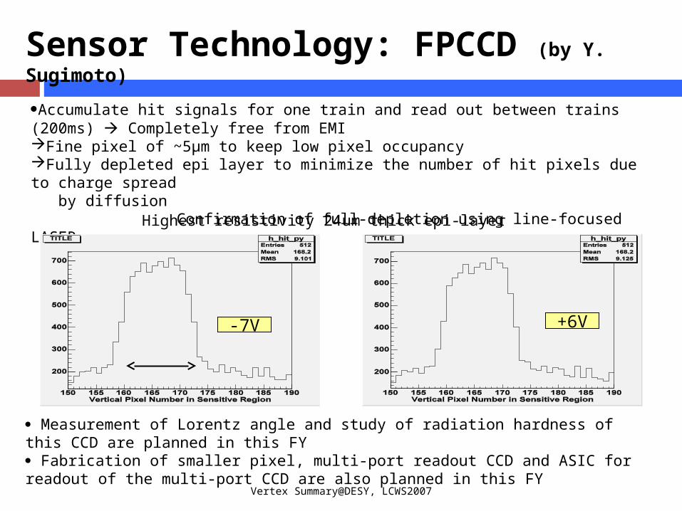
Sensor Technology: FPCCD (by Y. Sugimoto)
Accumulate hit signals for one train and read out between trains (200ms) Completely free from EMIFine pixel of ~5μm to keep low pixel occupancyFully depleted epi layer to minimize the number of hit pixels due to charge spread by diffusion Confirmation of full-depletion using line-focused LASER
-7V +6V
Highest resistivity 24um thick epi-layer
Measurement of Lorentz angle and study of radiation hardness of this CCD are planned in this FY Fabrication of smaller pixel, multi-port readout CCD and ASIC for readout of the multi-port CCD are also planned in this FY

Vertex Summary@DESY, LCWS2007
Sensor Technology: DEPFET (by L. Andricek)
Preparations for the new DEPFET generation are in full swing:
- New Sensors, larger matrices, with improved gain expected end of June 2007
- Steering chip Switcher operational and rad. hard
- New r/o chip submitted
Radiation tolerance of basic pixel cell proven for fluences far beyond the ones expected at the ILC .
irradiation TID / NIEL fluence ∆Vth gm ILeak in int. gate at RT(*)
gamma 60Co 913 krad / ~ 0 ~-4V unchanged 156 fA
neutron ~ 0 / 2.4x10¹¹ n/cm2 ~ 0 unchanged 1.4 pA
proton 283krad / 3x10¹² n/cm2 ~-5V ~ -15% 26 pA
(*) 5..22 fA non irrad.
New generation is almost done - very small pixels (20µm x 20µm) - increase internal amplification
long arrays(256 x 1024, ½ ILC)
wide arrays(512 x 512, full ILC)
various newstandard arrays(64 x 256 pixels,
down to 20x20µm2)
standard arrayscompatible to
existing hybrids
Rainer Richter, MPI HLL
long arrays(256 x 1024, ½ ILC)
wide arrays(512 x 512, full ILC)
various newstandard arrays(64 x 256 pixels,
down to 20x20µm2)
standard arrayscompatible to
existing hybrids
long arrays(256 x 1024, ½ ILC)
wide arrays(512 x 512, full ILC)
various newstandard arrays(64 x 256 pixels,
down to 20x20µm2)
standard arrayscompatible to
existing hybrids
Rainer Richter, MPI HLL

Vertex Summary@DESY, LCWS2007
Sensor Technology: CMOS (by A. Besson)
CMOS sensors developed for running conditions with beam background >> MC simulation (sizeable occupancy uncertainty)
General performances well established eff., S/N, fake hits, resolution, rad. hardness, moderate cooling AMS 0.35 µm OPTO techno assessed. Baseline for R & D new generation of full scale sensors underway:
real experimental conditions: equip EUDET, STAR, CBM demonstrator in 2007/2008 Fast read-out sensors progressing steadily
column // architecture with integrated discri. operationnal ADCs close to final design µcircuits: 1st generation close to fabrication
Milestones EUDET/STAR: final sensors with discri. binary charge encoding (2009 and 2010 resp.) replace discris by ADCs. Increase final read-out frequency find the final fabrication process (~< 0.2 µm)

Vertex Summary@DESY, LCWS2007
Sensor Technology: CMOS (by D. Contarato )
● Two prototypes of LDRD family produced and tested, exploring various pixel designs and architectures;
submission of next prototype with CP readout and 5-bit ADC in Summer
- second prototype chip in AMS 0.35
µm OPTO process, 14 um epilayer
- 20×20 µm2 pitch, 3×3 mm2 and 5×5
mm2 diodes
- Tests underway; study of
performance w.r.t. to clock
frequency, up to 25 MHz
Output
S R
SRAM-FIFO, NX x N
Y x 5 bits
Cref
Diode
Csig

Vertex Summary@DESY, LCWS2007
Sensor Technology: CMOS (by J. Brau )
Macro (50 um pitch) for timing Micro (5 um pitch) for precise position
563 transistors, 2 buffer, 50 um pixel (180nm tech)10~15 um pixel (45 nm tech):Much more tolerant to high background

Vertex Summary@DESY, LCWS2007
Emerging Sensor Technology: SOI & 3D (by S. Cihangir )
OKI 0.15 m SOI process (Mambo SOI X-Ray Chip)Counting pixel detector plus readout circuit - max counting rate ~1 MHz - 64x64 26 um pitch on 350 um thickness, 12 bit counterJust received tests are underway at Laser test stand.
Isolation from the bulk silicon: Lower parasitic capacitance and therefore faster switching and
lower power consumption… Enabling operation at higher temps (250oC)
At LBNL (by D. Contarato)● First prototype in OKI 0.15 um SOI technology (160x150 pixels, 10x10 um2 pixels)
just received, tests underway; next prototype submission in Fall '07 with optimized process.
3D integration (VIP1 chip, fabricated in MIT LL 0.18 m )
Vertex Summary@DESY, LCWS2007
Simulation Study - Effect of beamstrahhlung on VTX performance
- Pamametrization for MAPS response and Geant4 Simulation

Vertex Summary@DESY, LCWS2007
Simulation Study (by P. Luzniak and L. Maczewski)
14 mrad crossing angle MCS and energy loss VTX readout : 20 times per bunch train (1 readout cycle = 131 BX)
may possible distinguish between “physics” and “background” hits with help of variables describing hit cluster shape

Vertex Summary@DESY, LCWS2007
Integration Issue

Vertex Summary@DESY, LCWS2007
Integration: (by E. Johnson, M. Battaglia, L. Andricek)
SiC ladder
ladder block
glue
annulus block
Silicon Carbide Foam Ladder - 20 um thickness silicon - 1.5 mm thickness SiC foam - Silicone adhesive pads~0.14% X0
Reticulated Vitreous Carbon Foam/SiliconSandwich Ladder - 20 um thickness silicon - 1.5 mm thickness RVC foam - Silicone adhesive pads - Tension ~1.5 N~0.08% X0
20 μm deflection due to gravity
Continue prototyping foam ladder Finite Element Analysis is in progress Build and test carbon fibre shell
STAR
0.282% X0
DEPFET

Vertex Summary@DESY, LCWS2007
Outlook Advertise: global effort is starting to address integration issue across regions,technologies and concepts (regular phone meetings)
Oct. 2007 VTX R&D review at FNAL
not later than 2012: complete prototype ladder