Embed Size (px)
Citation preview
DPAK
SO-8
TO-92
Features• AEC-Q100 qualified (DPAK only)• Very low dropout voltage (90 mV typ. at 10 mA load)• Low quiescent current (typ. 2.5 mA, at 100 mA load)• Output current up to 100 mA• Adjustable (from VOUT = 2.5 V only SO-8) and fixed (3.3 V and 5 V) output
voltage version• Internal current and thermal limit• Load dump protection up to 60 V• Reverse transient protection up to - 50 V• Temperature range: - 40 to 125 °C• Package available: TO-92, DPAK, SO-8 (with inhibit control)
DescriptionThe LM2931 are very low drop regulators. The very low drop voltage and the lowquiescent current make them particular suitable for low noise, low power applicationsand in battery-powered systems. In the 8-pin configuration (SO-8), fully compatiblewith the older L78L family, a shutdown logic control function is available. This meansthat when the device is used as a local regulator it is possible to put a part of theboard in standby, decreasing total power consumption. Ideal for automotiveapplications, LM2931 is protected from reverse battery installations or 2 batteryjumps. During the transient, such as a 60 V load dump, when the input voltage canexceed the specified maximum operating input voltage of 26 V, the regulatorautomatically shuts down to protect both internal circuitry and the load.
Maturity status link
LM2931
Very low drop voltage regulators with inhibit function
LM2931
Datasheet
DS1760 - Rev 23 - February 2018For further information contact your local STMicroelectronics sales office.
www.st.com
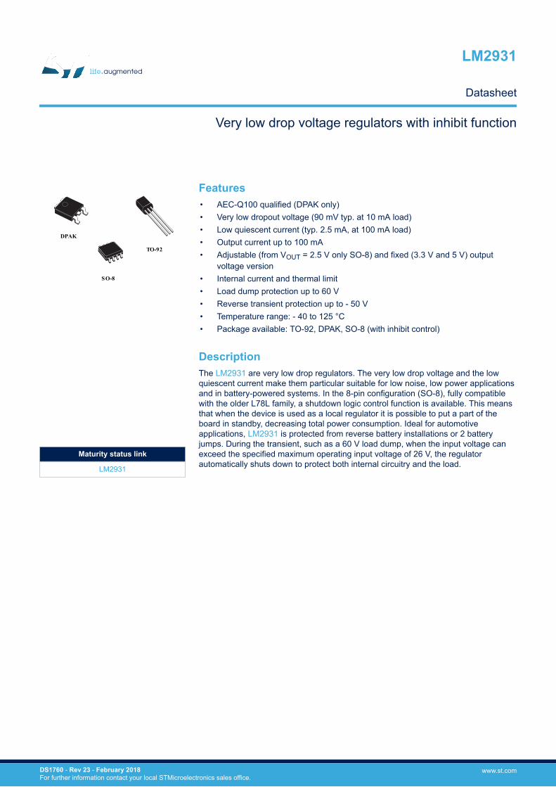
1 Diagram
Figure 2. Schematic diagram
AMG110720161100MT
LM2931Diagram
DS1760 - Rev 23 page 2/26
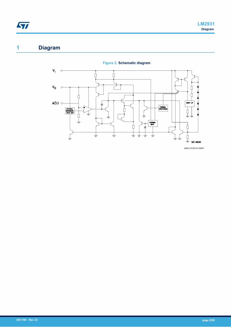
2 Pin configuration
Figure 3. Pin connections (top view)
SO-8DPAK
PIN 1 = VOUTPIN 2 = GNDPIN 3 = VIN
TO-92BOTTOM VIEW
GND
AMG110720161101MT
Note: (*) ADJ pin on the adjustable version, not connected in the fixed output version.
LM2931Pin configuration
DS1760 - Rev 23 page 3/26
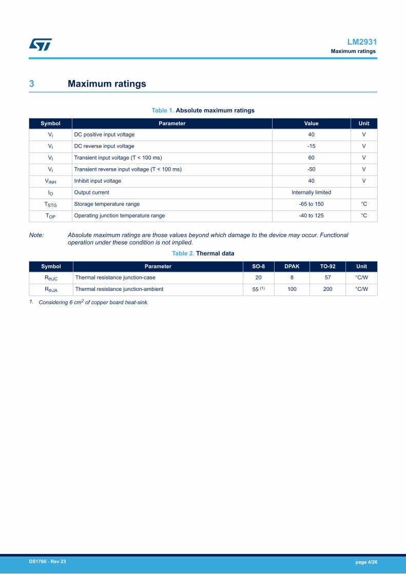
3 Maximum ratings
Table 1. Absolute maximum ratings
Symbol Parameter Value Unit
VI DC positive input voltage 40 V
VI DC reverse input voltage -15 V
VI Transient input voltage (Ƭ < 100 ms) 60 V
VI Transient reverse input voltage (Ƭ < 100 ms) -50 V
VINH Inhibit input voltage 40 V
IO Output current Internally limited
TSTG Storage temperature range -65 to 150 °C
TOP Operating junction temperature range -40 to 125 °C
Note: Absolute maximum ratings are those values beyond which damage to the device may occur. Functionaloperation under these condition is not implied.
Table 2. Thermal data
Symbol Parameter SO-8 DPAK TO-92 Unit
RthJC Thermal resistance junction-case 20 8 57 °C/W
RthJA Thermal resistance junction-ambient 55 (1) 100 200 °C/W
1. Considering 6 cm2 of copper board heat-sink.
LM2931Maximum ratings
DS1760 - Rev 23 page 4/26
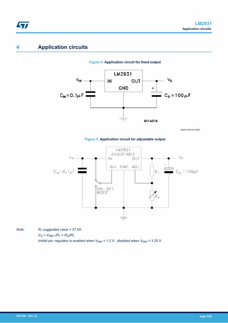
4 Application circuits
Figure 4. Application circuit for fixed output
AMG110720161102MT
Figure 5. Application circuit for adjustable output
Note: R1 suggested value = 27 kΩVO = VREF (R1 + R2)/R1
Inhibit pin: regulator is enabled when VINH < 1.2 V , disabled when VINH > 3.25 V
LM2931Application circuits
DS1760 - Rev 23 page 5/26
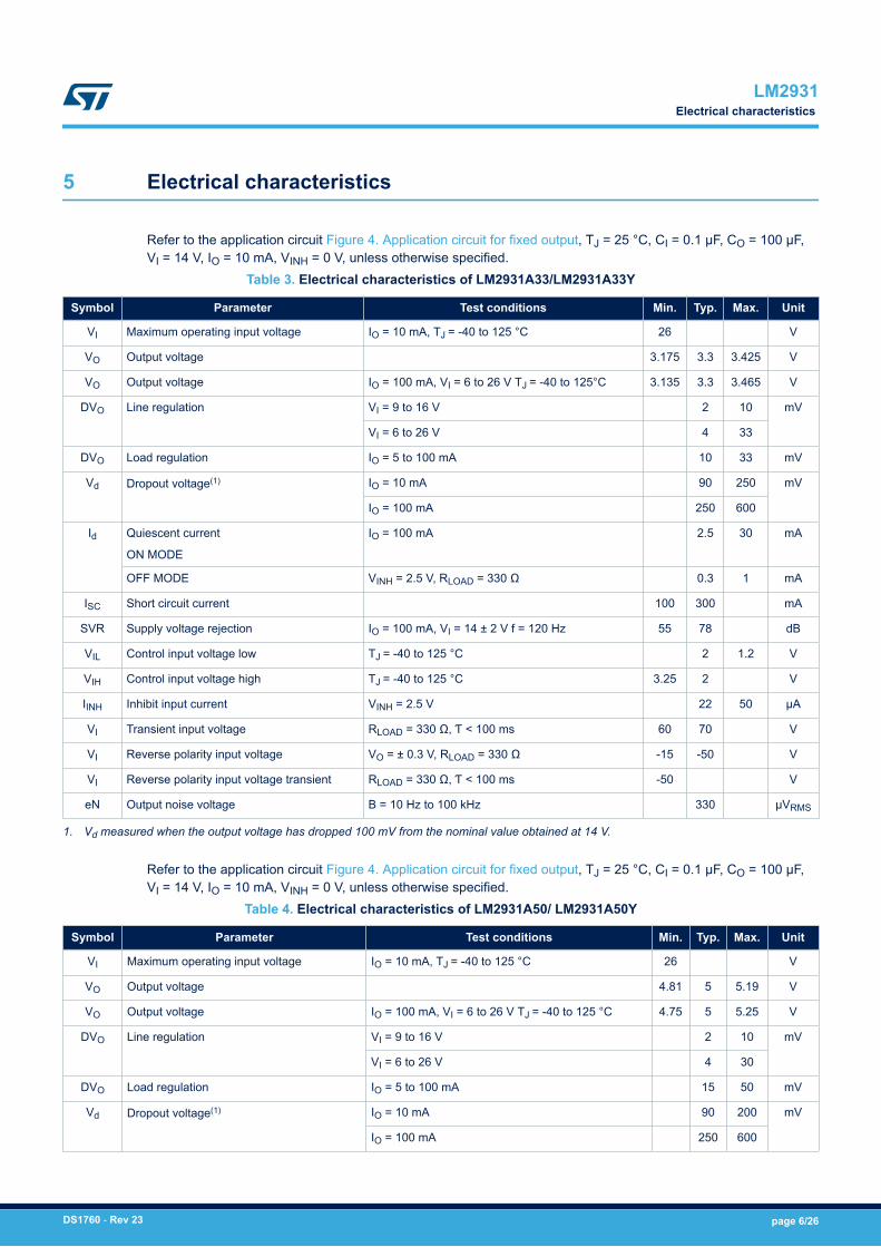
5 Electrical characteristics
Refer to the application circuit Figure 4. Application circuit for fixed output, TJ = 25 °C, CI = 0.1 µF, CO = 100 µF,VI = 14 V, IO = 10 mA, VINH = 0 V, unless otherwise specified.
Table 3. Electrical characteristics of LM2931A33/LM2931A33Y
Symbol Parameter Test conditions Min. Typ. Max. Unit
VI Maximum operating input voltage IO = 10 mA, TJ = -40 to 125 °C 26 V
VO Output voltage 3.175 3.3 3.425 V
VO Output voltage IO = 100 mA, VI = 6 to 26 V TJ = -40 to 125°C 3.135 3.3 3.465 V
DVO Line regulation VI = 9 to 16 V 2 10 mV
VI = 6 to 26 V 4 33
DVO Load regulation IO = 5 to 100 mA 10 33 mV
Vd Dropout voltage(1) IO = 10 mA 90 250 mV
IO = 100 mA 250 600
Id Quiescent current
ON MODE
IO = 100 mA 2.5 30 mA
OFF MODE VINH = 2.5 V, RLOAD = 330 Ω 0.3 1 mA
ISC Short circuit current 100 300 mA
SVR Supply voltage rejection IO = 100 mA, VI = 14 ± 2 V f = 120 Hz 55 78 dB
VIL Control input voltage low TJ = -40 to 125 °C 2 1.2 V
VIH Control input voltage high TJ = -40 to 125 °C 3.25 2 V
IINH Inhibit input current VINH = 2.5 V 22 50 µA
VI Transient input voltage RLOAD = 330 Ω, Ƭ < 100 ms 60 70 V
VI Reverse polarity input voltage VO = ± 0.3 V, RLOAD = 330 Ω -15 -50 V
VI Reverse polarity input voltage transient RLOAD = 330 Ω, Ƭ < 100 ms -50 V
eN Output noise voltage B = 10 Hz to 100 kHz 330 µVRMS
1. Vd measured when the output voltage has dropped 100 mV from the nominal value obtained at 14 V.
Refer to the application circuit Figure 4. Application circuit for fixed output, TJ = 25 °C, CI = 0.1 µF, CO = 100 µF,VI = 14 V, IO = 10 mA, VINH = 0 V, unless otherwise specified.
Table 4. Electrical characteristics of LM2931A50/ LM2931A50Y
Symbol Parameter Test conditions Min. Typ. Max. Unit
VI Maximum operating input voltage IO = 10 mA, TJ = -40 to 125 °C 26 V
VO Output voltage 4.81 5 5.19 V
VO Output voltage IO = 100 mA, VI = 6 to 26 V TJ = -40 to 125 °C 4.75 5 5.25 V
DVO Line regulation VI = 9 to 16 V 2 10 mV
VI = 6 to 26 V 4 30
DVO Load regulation IO = 5 to 100 mA 15 50 mV
Vd Dropout voltage(1) IO = 10 mA 90 200 mV
IO = 100 mA 250 600
LM2931Electrical characteristics
DS1760 - Rev 23 page 6/26
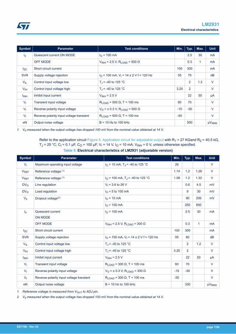
Symbol Parameter Test conditions Min. Typ. Max. Unit
Id Quiescent current ON MODE IO = 100 mA 2.5 30 mA
OFF MODE VINH = 2.5 V, RLOAD = 500 Ω 0.3 1 mA
ISC Short circuit current 100 300 mA
SVR Supply voltage rejection IO = 100 mA, VI = 14 ± 2 V f = 120 Hz 55 75 dB
VIL Control input voltage low TJ = -40 to 125 °C 2 1.2 V
VIH Control input voltage high TJ = -40 to 125 °C 3.25 2 V
IINH Inhibit input current VINH = 2.5 V 22 50 µA
VI Transient input voltage RLOAD = 500 Ω, Ƭ < 100 ms 60 70 V
VI Reverse polarity input voltage VO = ± 0.3 V, RLOAD = 500 Ω -15 -50 V
VI Reverse polarity input voltage transient RLOAD = 500 Ω, Ƭ < 100 ms -50 V
eN Output noise voltage B = 10 Hz to 100 kHz 500 µVRMS
1. Vd measured when the output voltage has dropped 100 mV from the nominal value obtained at 14 V.
Refer to the application circuit Figure 5. Application circuit for adjustable output with R1 = 27 KΩand R2 = 40.5 kΩ,TJ = 25 °C, CI = 0.1 µF, CO = 100 µF, VI = 14 V, IO = 10 mA, VINH = 0 V, unless otherwise specified.
Table 5. Electrical characteristics of LM2931 (adjustable version)
Symbol Parameter Test conditions Min. Typ. Max. Unit
VI Maximum operating input voltage IO = 10 mA, TJ = -40 to 125 °C 26 V
VREF Reference voltage (1) 1.14 1.2 1.26 V
VREF Reference voltage (1) IO = 100 mA, TJ = -40 to 125 °C 1.08 1.2 1.32 V
DVO Line regulation VI = 3.6 to 26 V 0.6 4.5 mV
DVO Load regulation IO = 5 to 100 mA 9 30 mV
Vd Dropout voltage(2) IO = 10 mA 90 200 mV
IO = 100 mA 250 600
Id Quiescent current
ON MODE
IO = 100 mA 2.5 30 mA
OFF MODE VINH = 2.5 V, RLOAD = 300 Ω 0.3 1 mA
ISC Short circuit current 100 300 mA
SVR Supply voltage rejection IO = 100 mA, VI = 14 ± 2 V f = 120 Hz 55 80 dB
VIL Control input voltage low TJ = -40 to 125 °C 2 1.2 V
VIH Control input voltage high TJ = -40 to 125 °C 3.25 2 V
IINH Inhibit input current VINH = 2.5 V 22 50 µA
VI Transient input voltage RLOAD = 300 Ω, Ƭ < 100 ms 60 70 V
VI Reverse polarity input voltage VO = ± 0.3 V, RLOAD = 300 Ω -15 -50 V
VI Reverse polarity input voltage transient RLOAD = 300 Ω, Ƭ < 100 ms -50 V
eN Output noise voltage B = 10 Hz to 100 kHz 330 µVRMS
1. Reference voltage is measured from VOUT to ADJ pin.
2. Vd measured when the output voltage has dropped 100 mV from the nominal value obtained at 14 V.
LM2931Electrical characteristics
DS1760 - Rev 23 page 7/26
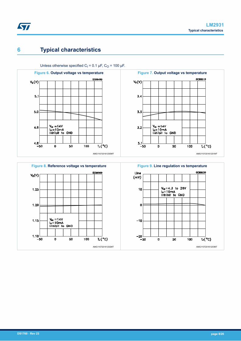
6 Typical characteristics
Unless otherwise specified CI = 0.1 µF, CO = 100 µF.
Figure 6. Output voltage vs temperature
AMG110720161200MT
Figure 7. Output voltage vs temperature
AMG110720161201MT
Figure 8. Reference voltage vs temperature
AMG110720161202MT
Figure 9. Line regulation vs temperature
AMG110720161203MT
LM2931Typical characteristics
DS1760 - Rev 23 page 8/26
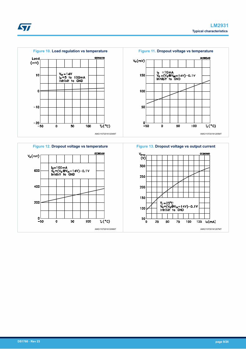
Figure 10. Load regulation vs temperature
AMG110720161204MT
Figure 11. Dropout voltage vs temperature
AMG110720161205MT
Figure 12. Dropout voltage vs temperature
AMG110720161206MT
Figure 13. Dropout voltage vs output current
AMG110720161207MT
LM2931Typical characteristics
DS1760 - Rev 23 page 9/26
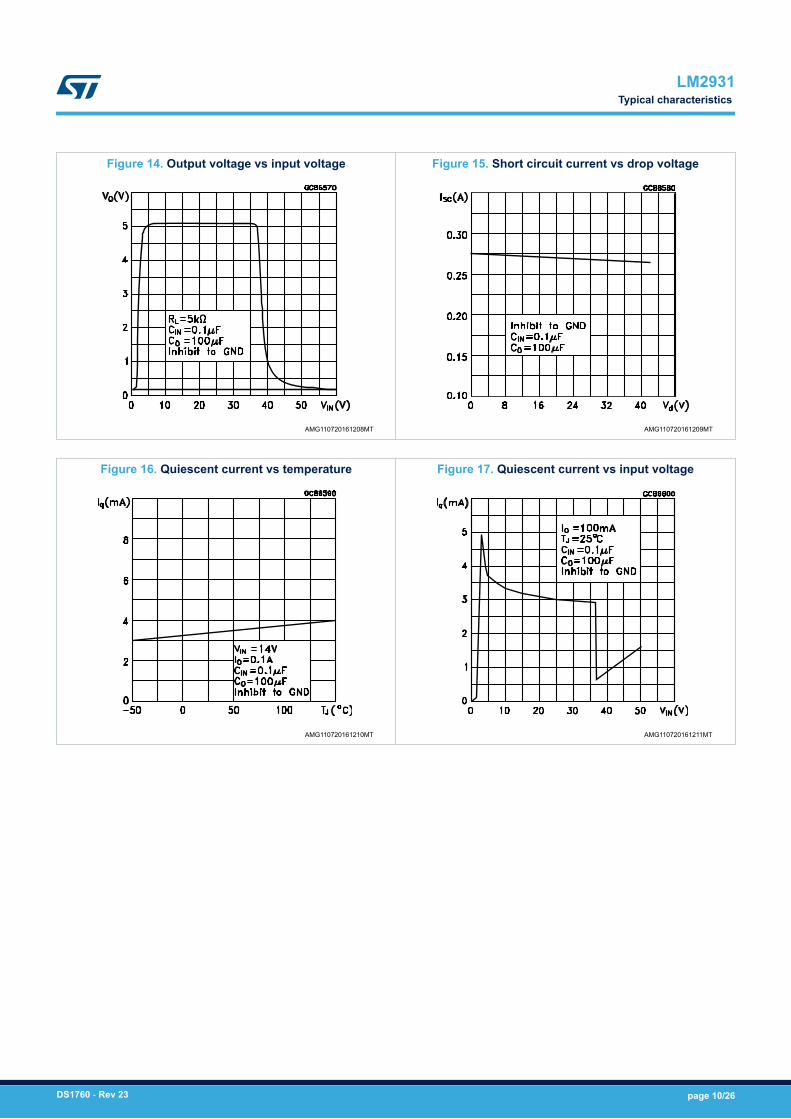
Figure 14. Output voltage vs input voltage
AMG110720161208MT
Figure 15. Short circuit current vs drop voltage
AMG110720161209MT
Figure 16. Quiescent current vs temperature
AMG110720161210MT
Figure 17. Quiescent current vs input voltage
AMG110720161211MT
LM2931Typical characteristics
DS1760 - Rev 23 page 10/26
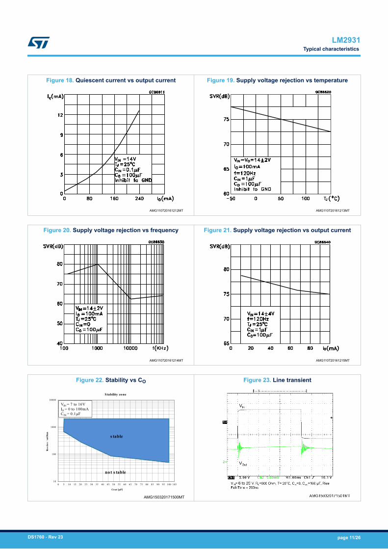
Figure 18. Quiescent current vs output current
AMG110720161212MT
Figure 19. Supply voltage rejection vs temperature
AMG110720161213MT
Figure 20. Supply voltage rejection vs frequency
AMG110720161214MT
Figure 21. Supply voltage rejection vs output current
AMG110720161215MT
Figure 22. Stability vs CO
10
100
1000
10000
0 5 10 15 20 25 30 35 40 45 50 55 60 65 70 75 80 85 90 95 100 105
Rse
ries
/ mO
hm
Cout [µF]
Stability zone
not s table
s table
VIN = 7 to 16VIO = 0 to 100mACIN = 0.1µF
AMG150320171500MT
Figure 23. Line transient
LM2931Typical characteristics
DS1760 - Rev 23 page 11/26
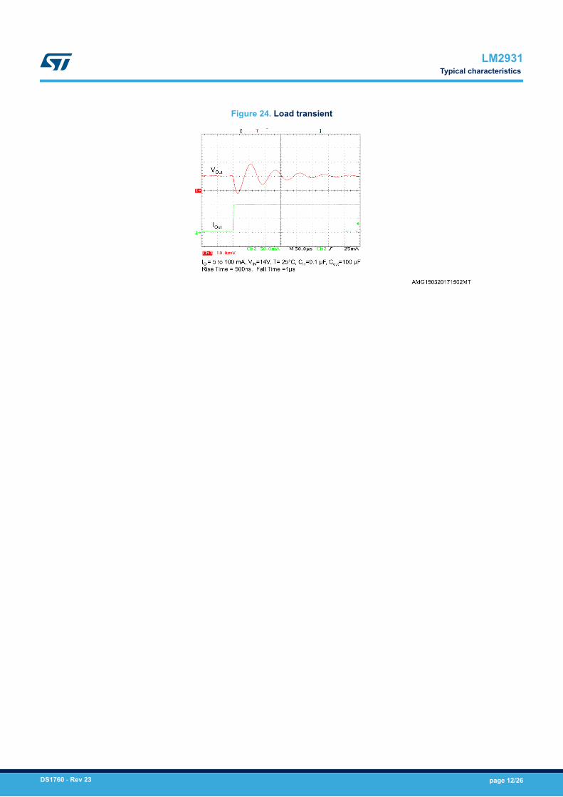
Figure 24. Load transient
LM2931Typical characteristics
DS1760 - Rev 23 page 12/26
7 Package information
In order to meet environmental requirements, ST offers these devices in different grades of ECOPACK®
packages, depending on their level of environmental compliance. ECOPACK® specifications, grade definitionsand product status are available at: www.st.com. ECOPACK® is an ST trademark.
LM2931Package information
DS1760 - Rev 23 page 13/26
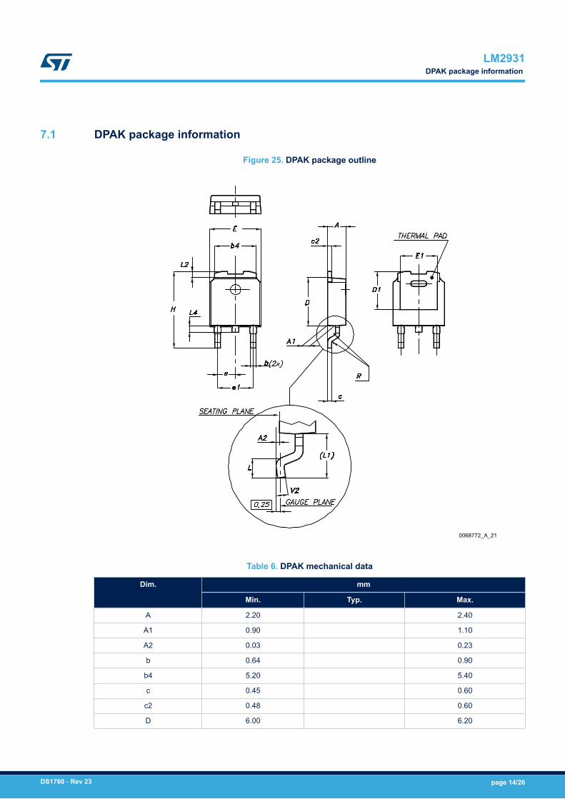
7.1 DPAK package information
Figure 25. DPAK package outline
0068772_A_21
Table 6. DPAK mechanical data
Dim. mm
Min. Typ. Max.
A 2.20 2.40
A1 0.90 1.10
A2 0.03 0.23
b 0.64 0.90
b4 5.20 5.40
c 0.45 0.60
c2 0.48 0.60
D 6.00 6.20
LM2931DPAK package information
DS1760 - Rev 23 page 14/26
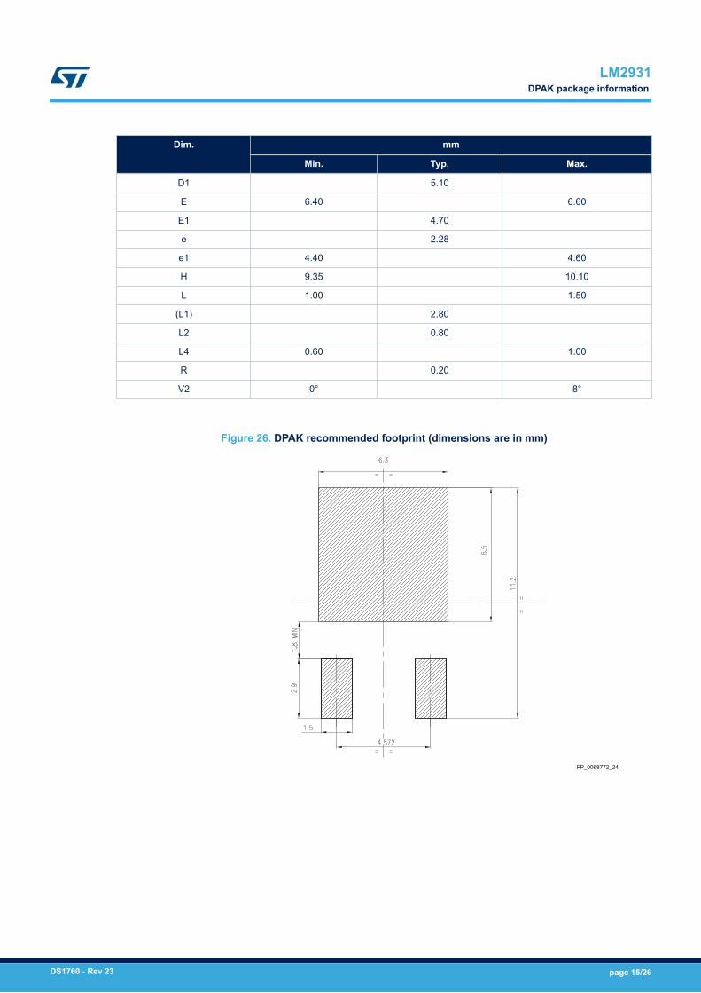
Dim. mm
Min. Typ. Max.
D1 5.10
E 6.40 6.60
E1 4.70
e 2.28
e1 4.40 4.60
H 9.35 10.10
L 1.00 1.50
(L1) 2.80
L2 0.80
L4 0.60 1.00
R 0.20
V2 0° 8°
Figure 26. DPAK recommended footprint (dimensions are in mm)
FP_0068772_24
LM2931DPAK package information
DS1760 - Rev 23 page 15/26
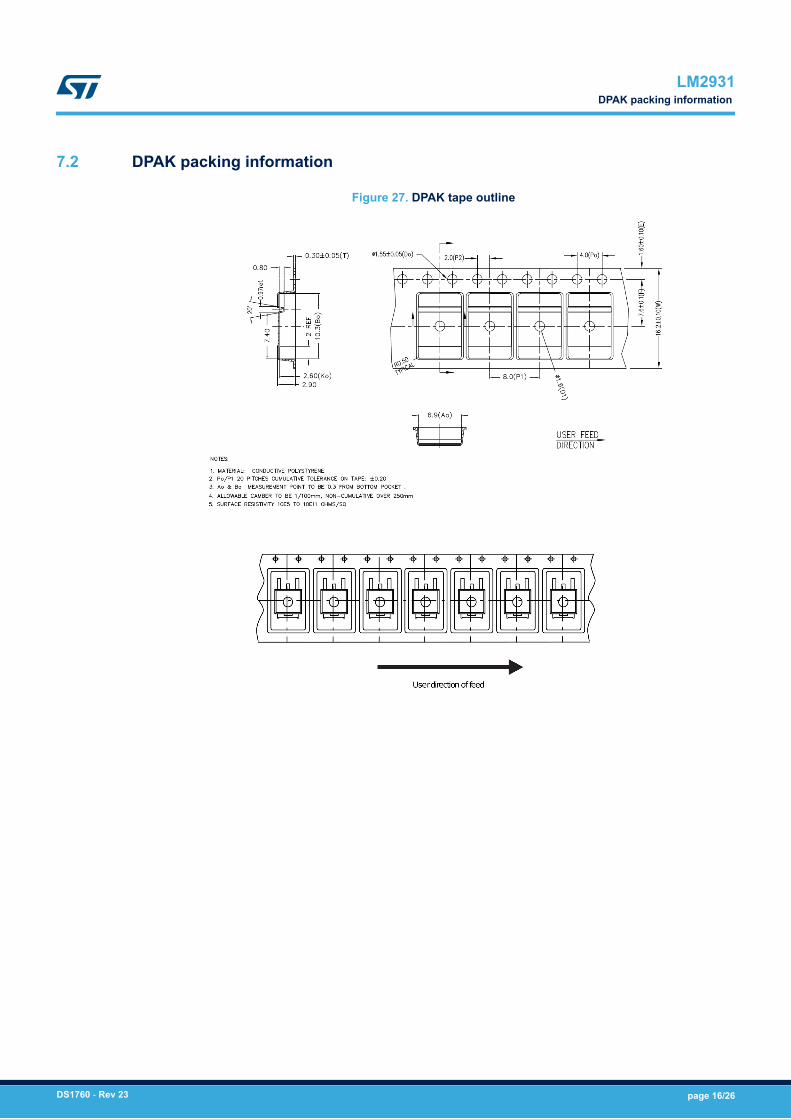
7.2 DPAK packing information
Figure 27. DPAK tape outline
LM2931DPAK packing information
DS1760 - Rev 23 page 16/26
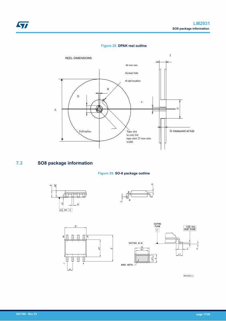
Figure 28. DPAK reel outline
A
D
B
Full radius G measured at hub
C
N
REEL DIMENSIONS
40 mm min.
Access hole
At slot location
T
Tape slot in core fortape start 25 mm min.width
7.3 SO8 package information
Figure 29. SO-8 package outline
0016023_I
LM2931SO8 package information
DS1760 - Rev 23 page 17/26
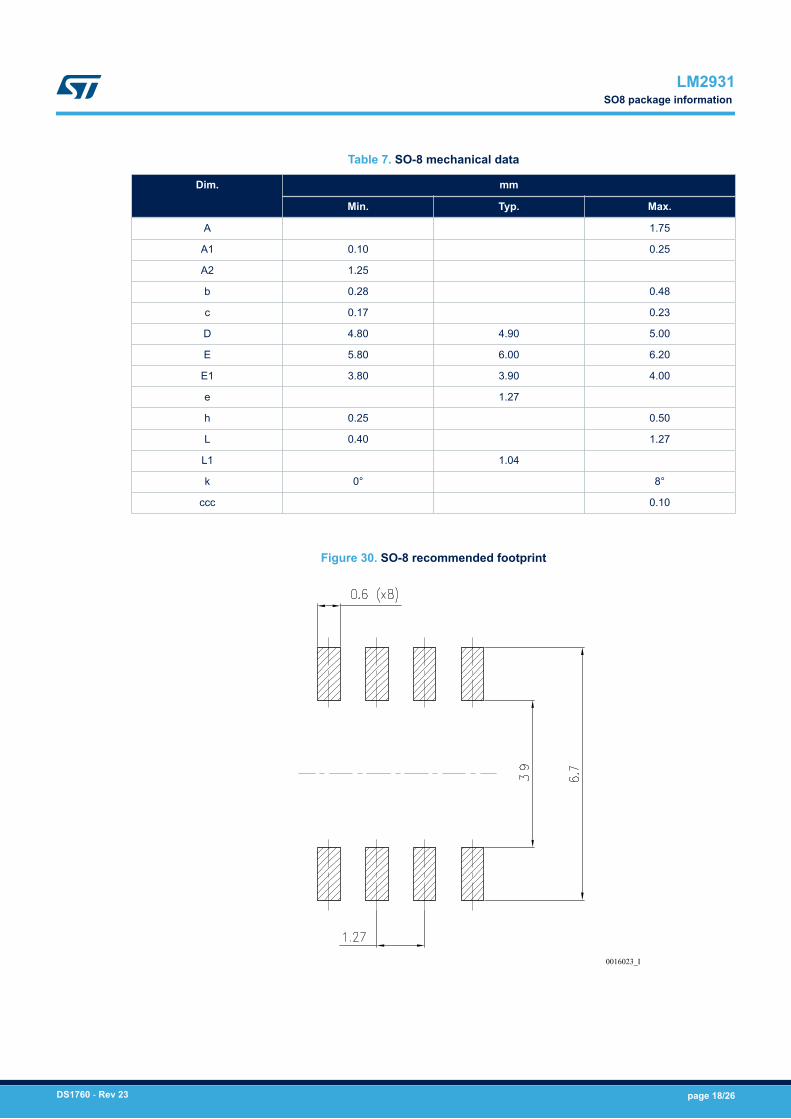
Table 7. SO-8 mechanical data
Dim. mm
Min. Typ. Max.
A 1.75
A1 0.10 0.25
A2 1.25
b 0.28 0.48
c 0.17 0.23
D 4.80 4.90 5.00
E 5.80 6.00 6.20
E1 3.80 3.90 4.00
e 1.27
h 0.25 0.50
L 0.40 1.27
L1 1.04
k 0° 8°
ccc 0.10
Figure 30. SO-8 recommended footprint
0016023_I
LM2931SO8 package information
DS1760 - Rev 23 page 18/26
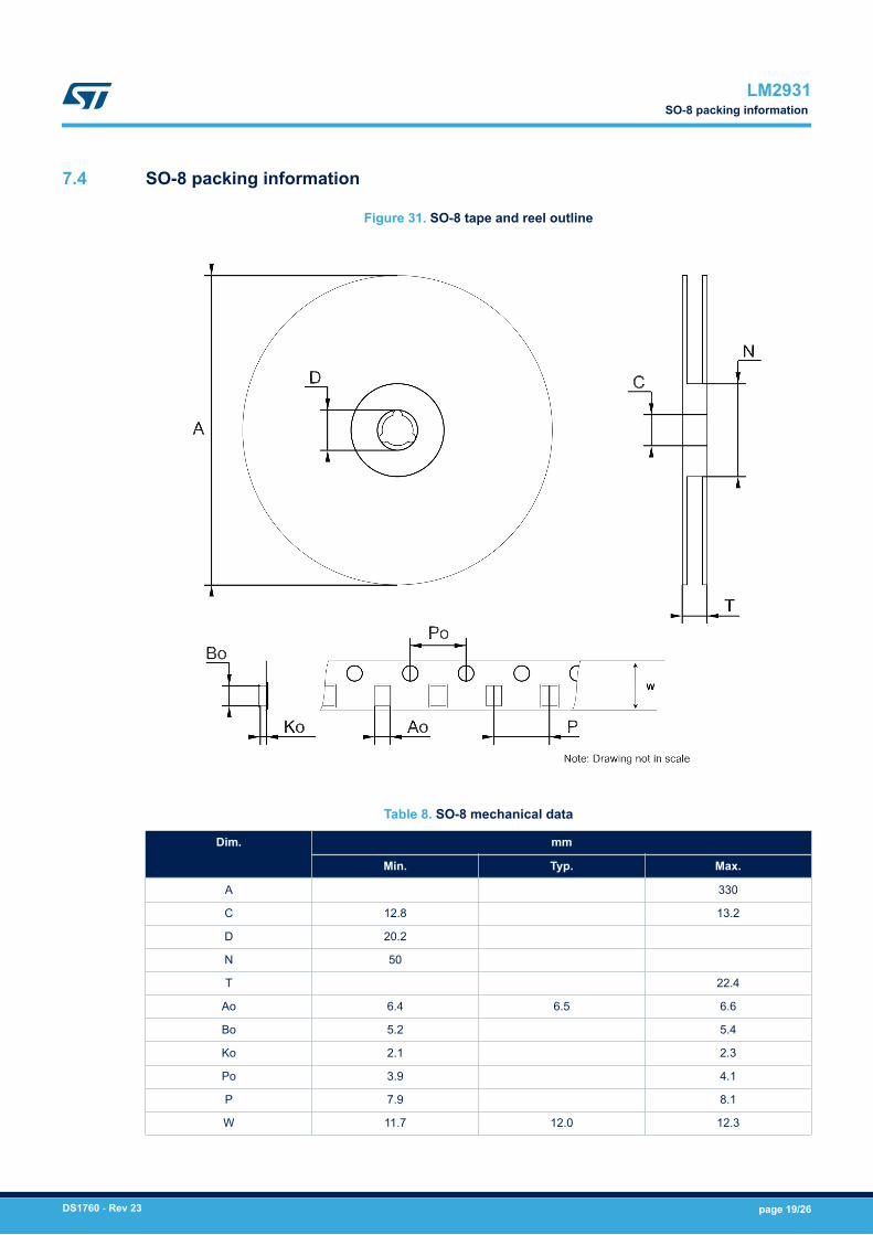
7.4 SO-8 packing information
Figure 31. SO-8 tape and reel outline
Table 8. SO-8 mechanical data
Dim. mm
Min. Typ. Max.
A 330
C 12.8 13.2
D 20.2
N 50
T 22.4
Ao 6.4 6.5 6.6
Bo 5.2 5.4
Ko 2.1 2.3
Po 3.9 4.1
P 7.9 8.1
W 11.7 12.0 12.3
LM2931SO-8 packing information
DS1760 - Rev 23 page 19/26
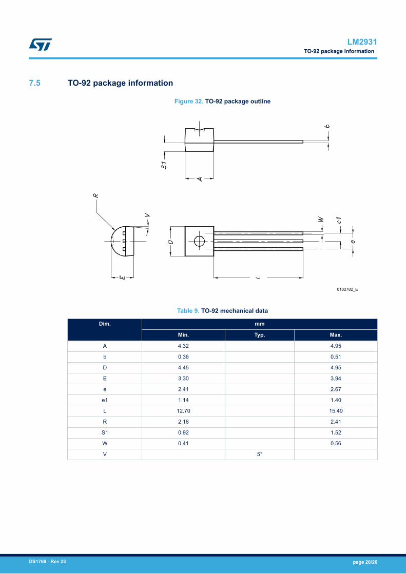
7.5 TO-92 package information
Figure 32. TO-92 package outline
0102782_E
Table 9. TO-92 mechanical data
Dim. mm
Min. Typ. Max.
A 4.32 4.95
b 0.36 0.51
D 4.45 4.95
E 3.30 3.94
e 2.41 2.67
e1 1.14 1.40
L 12.70 15.49
R 2.16 2.41
S1 0.92 1.52
W 0.41 0.56
V 5°
LM2931TO-92 package information
DS1760 - Rev 23 page 20/26
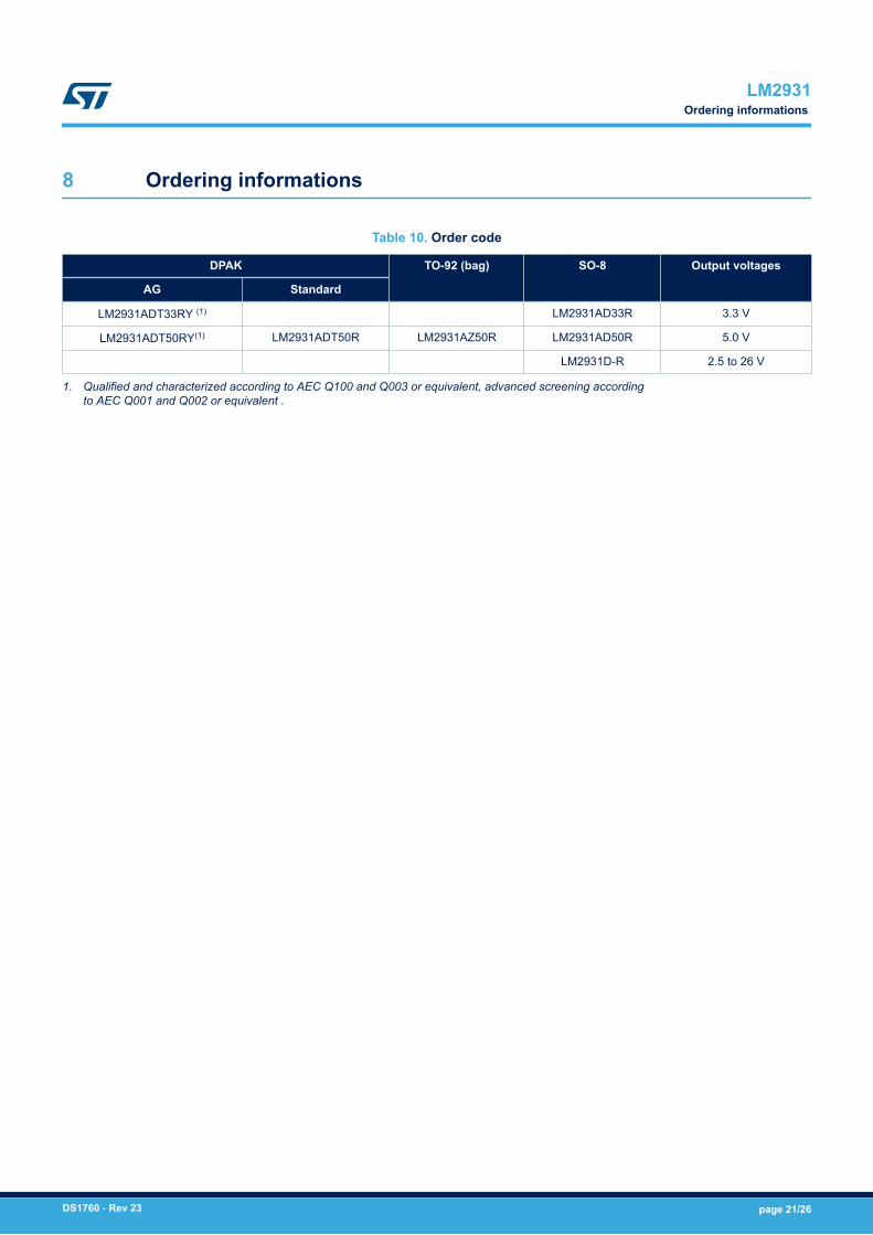
8 Ordering informations
Table 10. Order code
DPAK TO-92 (bag) SO-8 Output voltages
AG Standard
LM2931ADT33RY (1) LM2931AD33R 3.3 V
LM2931ADT50RY(1) LM2931ADT50R LM2931AZ50R LM2931AD50R 5.0 V
LM2931D-R 2.5 to 26 V
1. Qualified and characterized according to AEC Q100 and Q003 or equivalent, advanced screening accordingto AEC Q001 and Q002 or equivalent .
LM2931Ordering informations
DS1760 - Rev 23 page 21/26
Revision history
Table 11. Document revision history
Date Revision Changes
21-Jun-2004 12 Document updated.
16-Jun-2006 13 Order codes updated.
27-Jul-2007 14 Added Table 1 in cover page.
21-Aug-2007 15 Added root part number - (see Table 1).
22-Nov-2007 16 Modified: Table 1.
11-Feb-2008 17 Modified: Table 1 on page 1.
10-Jul-2008 18 Removed package TO-220, modified Table 1 on page 1.
26-May-2010 19 Modified: VI values Table 4 on page 6, Table 5 on page 7 andTable 6 on page 8.
02-Nov-2011 20 Modified: Figure 4 on page 6. Added: (*) ADJ pin on theAdjustable version, Not Connected in the fixed output version.on page 4 and Inhibit pin: regulator is enabled when VINH < 1.2V , disabled when VINH > 3.25 V on page 6.
09-Apr-2014 21 Part numbers LM2931XX, LM2931AXX33 and LM2931AXX50changed to LM2931. Updated the description in cover pageSection 2: Pin configuration and Section 7: Packageinformation. Added Section 8: Revision history. Minor textchanges.
16-Mar-2017 22 Updated features in cover page, removed Table 1. Devicesummary from cover page, Table 3: "Electrical characteristics ofLM2931A33/LM2931A33Y" , Table 4: "Electrical characteristicsof LM2931A50/ LM2931A50Y" and Table 5: "Electricalcharacteristics of LM2931 (adjustable version)".
Updated Section 7: "Package information".
Added Section 8: "Ordering information".
Minor text changes.
23-Feb-2018 23 Updated Figure 5. Application circuit for adjustable output.
LM2931
DS1760 - Rev 23 page 22/26
Contents
1 Diagram . . . . . . . . . . . . . . . . . . . . . . . . . . . . . . . . . . . . . . . . . . . . . . . . . . . . . . . . . . . . . . . . . . . . . . . . . . .2
2 Pin configuration . . . . . . . . . . . . . . . . . . . . . . . . . . . . . . . . . . . . . . . . . . . . . . . . . . . . . . . . . . . . . . . . . .3
3 Maximum ratings . . . . . . . . . . . . . . . . . . . . . . . . . . . . . . . . . . . . . . . . . . . . . . . . . . . . . . . . . . . . . . . . . .4
4 Application circuits . . . . . . . . . . . . . . . . . . . . . . . . . . . . . . . . . . . . . . . . . . . . . . . . . . . . . . . . . . . . . . . .5
5 Electrical characteristics. . . . . . . . . . . . . . . . . . . . . . . . . . . . . . . . . . . . . . . . . . . . . . . . . . . . . . . . . . .6
6 Typical characteristics . . . . . . . . . . . . . . . . . . . . . . . . . . . . . . . . . . . . . . . . . . . . . . . . . . . . . . . . . . . . .8
7 Package information. . . . . . . . . . . . . . . . . . . . . . . . . . . . . . . . . . . . . . . . . . . . . . . . . . . . . . . . . . . . . .13
7.1 DPAK package information . . . . . . . . . . . . . . . . . . . . . . . . . . . . . . . . . . . . . . . . . . . . . . . . . . . . . 14
7.2 DPAK packing information . . . . . . . . . . . . . . . . . . . . . . . . . . . . . . . . . . . . . . . . . . . . . . . . . . . . . 15
7.3 SO8 package information . . . . . . . . . . . . . . . . . . . . . . . . . . . . . . . . . . . . . . . . . . . . . . . . . . . . . . 17
7.4 SO-8 packing information . . . . . . . . . . . . . . . . . . . . . . . . . . . . . . . . . . . . . . . . . . . . . . . . . . . . . . 18
7.5 TO-92 package information . . . . . . . . . . . . . . . . . . . . . . . . . . . . . . . . . . . . . . . . . . . . . . . . . . . . 19
8 Ordering informations . . . . . . . . . . . . . . . . . . . . . . . . . . . . . . . . . . . . . . . . . . . . . . . . . . . . . . . . . . . .21
Revision history . . . . . . . . . . . . . . . . . . . . . . . . . . . . . . . . . . . . . . . . . . . . . . . . . . . . . . . . . . . . . . . . . . . . . . .22
Contents . . . . . . . . . . . . . . . . . . . . . . . . . . . . . . . . . . . . . . . . . . . . . . . . . . . . . . . . . . . . . . . . . . . . . . . . . . . . . .23
List of tables . . . . . . . . . . . . . . . . . . . . . . . . . . . . . . . . . . . . . . . . . . . . . . . . . . . . . . . . . . . . . . . . . . . . . . . . . .24
List of figures. . . . . . . . . . . . . . . . . . . . . . . . . . . . . . . . . . . . . . . . . . . . . . . . . . . . . . . . . . . . . . . . . . . . . . . . . .25
Disclaimer . . . . . . . . . . . . . . . . . . . . . . . . . . . . . . . . . . . . . . . . . . . . . . . . . . . . . . . . . . . . . . . . . . . . . . . . . . . . .26
LM2931Contents
DS1760 - Rev 23 page 23/26
List of tablesTable 1. Absolute maximum ratings . . . . . . . . . . . . . . . . . . . . . . . . . . . . . . . . . . . . . . . . . . . . . . . . . . . . . . . . . . . . . 4Table 2. Thermal data. . . . . . . . . . . . . . . . . . . . . . . . . . . . . . . . . . . . . . . . . . . . . . . . . . . . . . . . . . . . . . . . . . . . . . . 4Table 3. Electrical characteristics of LM2931A33/LM2931A33Y . . . . . . . . . . . . . . . . . . . . . . . . . . . . . . . . . . . . . . . . . . 6Table 4. Electrical characteristics of LM2931A50/ LM2931A50Y. . . . . . . . . . . . . . . . . . . . . . . . . . . . . . . . . . . . . . . . . . 6Table 5. Electrical characteristics of LM2931 (adjustable version) . . . . . . . . . . . . . . . . . . . . . . . . . . . . . . . . . . . . . . . . . 7Table 6. DPAK mechanical data . . . . . . . . . . . . . . . . . . . . . . . . . . . . . . . . . . . . . . . . . . . . . . . . . . . . . . . . . . . . . . . 14Table 7. SO-8 mechanical data . . . . . . . . . . . . . . . . . . . . . . . . . . . . . . . . . . . . . . . . . . . . . . . . . . . . . . . . . . . . . . . 18Table 8. SO-8 mechanical data . . . . . . . . . . . . . . . . . . . . . . . . . . . . . . . . . . . . . . . . . . . . . . . . . . . . . . . . . . . . . . . 19Table 9. TO-92 mechanical data. . . . . . . . . . . . . . . . . . . . . . . . . . . . . . . . . . . . . . . . . . . . . . . . . . . . . . . . . . . . . . . 20Table 10. Order code . . . . . . . . . . . . . . . . . . . . . . . . . . . . . . . . . . . . . . . . . . . . . . . . . . . . . . . . . . . . . . . . . . . . . . . 21Table 11. Document revision history . . . . . . . . . . . . . . . . . . . . . . . . . . . . . . . . . . . . . . . . . . . . . . . . . . . . . . . . . . . . . 22
LM2931List of tables
DS1760 - Rev 23 page 24/26
List of figuresFigure 2. Schematic diagram . . . . . . . . . . . . . . . . . . . . . . . . . . . . . . . . . . . . . . . . . . . . . . . . . . . . . . . . . . . . . . . . . 2Figure 3. Pin connections (top view) . . . . . . . . . . . . . . . . . . . . . . . . . . . . . . . . . . . . . . . . . . . . . . . . . . . . . . . . . . . . 3Figure 4. Application circuit for fixed output . . . . . . . . . . . . . . . . . . . . . . . . . . . . . . . . . . . . . . . . . . . . . . . . . . . . . . . 5Figure 5. Application circuit for adjustable output . . . . . . . . . . . . . . . . . . . . . . . . . . . . . . . . . . . . . . . . . . . . . . . . . . . 5Figure 6. Output voltage vs temperature . . . . . . . . . . . . . . . . . . . . . . . . . . . . . . . . . . . . . . . . . . . . . . . . . . . . . . . . . 8Figure 7. Output voltage vs temperature . . . . . . . . . . . . . . . . . . . . . . . . . . . . . . . . . . . . . . . . . . . . . . . . . . . . . . . . . 8Figure 8. Reference voltage vs temperature. . . . . . . . . . . . . . . . . . . . . . . . . . . . . . . . . . . . . . . . . . . . . . . . . . . . . . . 8Figure 9. Line regulation vs temperature . . . . . . . . . . . . . . . . . . . . . . . . . . . . . . . . . . . . . . . . . . . . . . . . . . . . . . . . . 8Figure 10. Load regulation vs temperature. . . . . . . . . . . . . . . . . . . . . . . . . . . . . . . . . . . . . . . . . . . . . . . . . . . . . . . . . 9Figure 11. Dropout voltage vs temperature . . . . . . . . . . . . . . . . . . . . . . . . . . . . . . . . . . . . . . . . . . . . . . . . . . . . . . . . 9Figure 12. Dropout voltage vs temperature . . . . . . . . . . . . . . . . . . . . . . . . . . . . . . . . . . . . . . . . . . . . . . . . . . . . . . . . 9Figure 13. Dropout voltage vs output current . . . . . . . . . . . . . . . . . . . . . . . . . . . . . . . . . . . . . . . . . . . . . . . . . . . . . . . 9Figure 14. Output voltage vs input voltage . . . . . . . . . . . . . . . . . . . . . . . . . . . . . . . . . . . . . . . . . . . . . . . . . . . . . . . . 10Figure 15. Short circuit current vs drop voltage. . . . . . . . . . . . . . . . . . . . . . . . . . . . . . . . . . . . . . . . . . . . . . . . . . . . . 10Figure 16. Quiescent current vs temperature . . . . . . . . . . . . . . . . . . . . . . . . . . . . . . . . . . . . . . . . . . . . . . . . . . . . . . 10Figure 17. Quiescent current vs input voltage . . . . . . . . . . . . . . . . . . . . . . . . . . . . . . . . . . . . . . . . . . . . . . . . . . . . . 10Figure 18. Quiescent current vs output current . . . . . . . . . . . . . . . . . . . . . . . . . . . . . . . . . . . . . . . . . . . . . . . . . . . . . 11Figure 19. Supply voltage rejection vs temperature. . . . . . . . . . . . . . . . . . . . . . . . . . . . . . . . . . . . . . . . . . . . . . . . . . 11Figure 20. Supply voltage rejection vs frequency . . . . . . . . . . . . . . . . . . . . . . . . . . . . . . . . . . . . . . . . . . . . . . . . . . . 11Figure 21. Supply voltage rejection vs output current . . . . . . . . . . . . . . . . . . . . . . . . . . . . . . . . . . . . . . . . . . . . . . . . 11Figure 22. Stability vs CO . . . . . . . . . . . . . . . . . . . . . . . . . . . . . . . . . . . . . . . . . . . . . . . . . . . . . . . . . . . . . . . . . . . 11Figure 23. Line transient . . . . . . . . . . . . . . . . . . . . . . . . . . . . . . . . . . . . . . . . . . . . . . . . . . . . . . . . . . . . . . . . . . . . 11Figure 24. Load transient . . . . . . . . . . . . . . . . . . . . . . . . . . . . . . . . . . . . . . . . . . . . . . . . . . . . . . . . . . . . . . . . . . . 12Figure 25. DPAK package outline . . . . . . . . . . . . . . . . . . . . . . . . . . . . . . . . . . . . . . . . . . . . . . . . . . . . . . . . . . . . . . 14Figure 26. DPAK recommended footprint (dimensions are in mm). . . . . . . . . . . . . . . . . . . . . . . . . . . . . . . . . . . . . . . . 15Figure 27. DPAK tape outline. . . . . . . . . . . . . . . . . . . . . . . . . . . . . . . . . . . . . . . . . . . . . . . . . . . . . . . . . . . . . . . . . 16Figure 28. DPAK reel outline . . . . . . . . . . . . . . . . . . . . . . . . . . . . . . . . . . . . . . . . . . . . . . . . . . . . . . . . . . . . . . . . . 17Figure 29. SO-8 package outline . . . . . . . . . . . . . . . . . . . . . . . . . . . . . . . . . . . . . . . . . . . . . . . . . . . . . . . . . . . . . . 17Figure 30. SO-8 recommended footprint . . . . . . . . . . . . . . . . . . . . . . . . . . . . . . . . . . . . . . . . . . . . . . . . . . . . . . . . . 18Figure 31. SO-8 tape and reel outline . . . . . . . . . . . . . . . . . . . . . . . . . . . . . . . . . . . . . . . . . . . . . . . . . . . . . . . . . . . 19Figure 32. TO-92 package outline . . . . . . . . . . . . . . . . . . . . . . . . . . . . . . . . . . . . . . . . . . . . . . . . . . . . . . . . . . . . . 20
LM2931List of figures
DS1760 - Rev 23 page 25/26
IMPORTANT NOTICE – PLEASE READ CAREFULLY
STMicroelectronics NV and its subsidiaries (“ST”) reserve the right to make changes, corrections, enhancements, modifications, and improvements to STproducts and/or to this document at any time without notice. Purchasers should obtain the latest relevant information on ST products before placing orders. STproducts are sold pursuant to ST’s terms and conditions of sale in place at the time of order acknowledgement.
Purchasers are solely responsible for the choice, selection, and use of ST products and ST assumes no liability for application assistance or the design ofPurchasers’ products.
No license, express or implied, to any intellectual property right is granted by ST herein.
Resale of ST products with provisions different from the information set forth herein shall void any warranty granted by ST for such product.
ST and the ST logo are trademarks of ST. All other product or service names are the property of their respective owners.
Information in this document supersedes and replaces information previously supplied in any prior versions of this document.
© 2018 STMicroelectronics – All rights reserved
LM2931
DS1760 - Rev 23 page 26/26

![EVOLUTION OF VOLTAGE REGULATOR TO … · Low Drop out (CL-LDO) Voltage Regulator, since CL-LDO architecture is the ... portable, handheld battery operated devices [1]. Voltage regulators](https://img.pdfslide.net/doc/110x75/5b91ca6e09d3f26a278c8323/evolution-of-voltage-regulator-to-low-drop-out-cl-ldo-voltage-regulator-since.jpg)