Embed Size (px)
Citation preview

This is information on a product in full production.
March 2012 Doc ID 2574 Rev 26 1/50
50
LFxxABLFxxC
Very low drop voltage regulators with inhibit
Datasheet − production data
Features■ Very low dropout voltage (0.45 V)
■ Very low quiescent current (typ. 50 µA in OFF mode, 500 µA in ON mode)
■ Output current up to 500 mA
■ Logic-controlled electronic shutdown
■ Output voltages of 1.5; 1.8; 2.5; 3.3; 4.7; 5; 6; 8; 8.5; 9; 12 V
■ Automotive Grade product: 1.8 V, 2.5 V, 3.3 V, 5.0 V, 8.0 V, 8.5 V VOUT in DPAK and PPAK packages
■ Internal current and thermal limit
■ Only 2.2 µF for stability
■ Available in ± 1 % (AB) or ± 2 % (C) selection at 25 °C
■ Supply voltage rejection: 80 db (typ.)
■ Temperature range: -40 to 125 °C
DescriptionThe LFxxAB/LFxxC are very low drop regulators available in PENTAWATT, TO-220, TO-220FP, DPAK and PPAK package and in a wide range of output voltages. The very low drop voltage (0.45 V) and the very low quiescent current make them particularly suitable for low noise, low power applications and specially in battery powered systems. In the 5 pins configuration (PENTAWATT and PPAK) a shutdown logic control function is available (pin 2, TTL compatible). This means that when the device is used as a local regulator, it is possible to put a part of the board in standby,
decreasing the total power consumption. In the three terminal configuration the device has the same electrical performance, but is fixed in the ON state. It requires only a 2.2 µF capacitor for stability allowing space and cost saving. The LFxx is available as Automotive Grade in DPAK and PPAK packages, for the options of output voltages whose commercial part numbers are shown in the order codes. These devices are qualified according to the specification AEC-Q100 of the Automotive market, in the temperature range - 40 °C to 125 °C, and the statistical tests PAT, SYL, SBL are performed.
TO-220FP
PENTAWATT
TO-220
DPAKPPAK
Table 1. Device summary
Part numbers
LF15AB LF25C LF33AB LF60C LF80AB LF120C
LF18C LF25AB LF50C LF60AB LF85C LF120AB
LF18AB LF33C LF50AB LF80C LF90C
www.st.com

Contents LFxxAB, LFxxC
2/50 Doc ID 2574 Rev 26
Contents
1 Diagram . . . . . . . . . . . . . . . . . . . . . . . . . . . . . . . . . . . . . . . . . . . . . . . . . . . 5
2 Pin configuration . . . . . . . . . . . . . . . . . . . . . . . . . . . . . . . . . . . . . . . . . . . 6
3 Maximum ratings . . . . . . . . . . . . . . . . . . . . . . . . . . . . . . . . . . . . . . . . . . . . 7
4 Electrical characteristics . . . . . . . . . . . . . . . . . . . . . . . . . . . . . . . . . . . . . 8
5 Typical performance characteristics . . . . . . . . . . . . . . . . . . . . . . . . . . . 35
6 Package mechanical data . . . . . . . . . . . . . . . . . . . . . . . . . . . . . . . . . . . . 39
7 Order codes . . . . . . . . . . . . . . . . . . . . . . . . . . . . . . . . . . . . . . . . . . . . . . . 48
8 Revision history . . . . . . . . . . . . . . . . . . . . . . . . . . . . . . . . . . . . . . . . . . . 49

LFxxAB, LFxxC List of tables
Doc ID 2574 Rev 26 3/50
List of tables
Table 1. Device summary . . . . . . . . . . . . . . . . . . . . . . . . . . . . . . . . . . . . . . . . . . . . . . . . . . . . . . . . . . 1Table 2. Absolute maximum ratings . . . . . . . . . . . . . . . . . . . . . . . . . . . . . . . . . . . . . . . . . . . . . . . . . . 7Table 3. Thermal data. . . . . . . . . . . . . . . . . . . . . . . . . . . . . . . . . . . . . . . . . . . . . . . . . . . . . . . . . . . . . 7Table 4. Electrical characteristics for LF15AB . . . . . . . . . . . . . . . . . . . . . . . . . . . . . . . . . . . . . . . . . . 8Table 5. Electrical characteristics for LF18AB . . . . . . . . . . . . . . . . . . . . . . . . . . . . . . . . . . . . . . . . . . 9Table 6. Electrical characteristics for LF18C . . . . . . . . . . . . . . . . . . . . . . . . . . . . . . . . . . . . . . . . . . 10Table 7. Electrical characteristics for LF18CDT-TRY (Automotive Grade). . . . . . . . . . . . . . . . . . . . 11Table 8. Electrical characteristics for LF25AB . . . . . . . . . . . . . . . . . . . . . . . . . . . . . . . . . . . . . . . . . 12Table 9. Electrical characteristics for LF25ABDT-TRY (Automotive Grade). . . . . . . . . . . . . . . . . . . 13Table 10. Electrical characteristics for LF25C . . . . . . . . . . . . . . . . . . . . . . . . . . . . . . . . . . . . . . . . . . 14Table 11. Electrical characteristics for LF25CDT-TRY (Automotive Grade). . . . . . . . . . . . . . . . . . . . 15Table 12. Electrical characteristics for LF33AB . . . . . . . . . . . . . . . . . . . . . . . . . . . . . . . . . . . . . . . . . 16Table 13. Electrical characteristics for LF33C . . . . . . . . . . . . . . . . . . . . . . . . . . . . . . . . . . . . . . . . . . 17Table 14. Electrical characteristics for LF33CDT-TRY and LF33CPT-TRY (Automotive Grade) . . . . 18Table 15. Electrical characteristics for LF50AB . . . . . . . . . . . . . . . . . . . . . . . . . . . . . . . . . . . . . . . . . 19Table 16. Electrical characteristics for LF50ABDT-TRY (Automotive Grade). . . . . . . . . . . . . . . . . . . 20Table 17. Electrical characteristics for LF50C . . . . . . . . . . . . . . . . . . . . . . . . . . . . . . . . . . . . . . . . . . 21Table 18. Electrical characteristics for LF50CDT-TRY and LF50CPT-TRY (Automotive Grade) . . . . 22Table 19. Electrical characteristics for LF60AB . . . . . . . . . . . . . . . . . . . . . . . . . . . . . . . . . . . . . . . . . 23Table 20. Electrical characteristics for LF60C . . . . . . . . . . . . . . . . . . . . . . . . . . . . . . . . . . . . . . . . . . 24Table 21. Electrical characteristics for LF80AB . . . . . . . . . . . . . . . . . . . . . . . . . . . . . . . . . . . . . . . . . 25Table 22. Electrical characteristics for LF80C . . . . . . . . . . . . . . . . . . . . . . . . . . . . . . . . . . . . . . . . . . 26Table 23. Electrical characteristics for LF80CDT-TRY (Automotive Grade). . . . . . . . . . . . . . . . . . . . 27Table 24. Electrical characteristics for LF85AB . . . . . . . . . . . . . . . . . . . . . . . . . . . . . . . . . . . . . . . . . 28Table 25. Electrical characteristics for LF85C . . . . . . . . . . . . . . . . . . . . . . . . . . . . . . . . . . . . . . . . . . 29Table 26. Electrical characteristics for LF85CDT-TRY and LF85CPT-TRY (Automotive Grade) . . . . 30Table 27. Electrical characteristics for LF90AB . . . . . . . . . . . . . . . . . . . . . . . . . . . . . . . . . . . . . . . . . 31Table 28. Electrical characteristics for LF90C . . . . . . . . . . . . . . . . . . . . . . . . . . . . . . . . . . . . . . . . . . 32Table 29. Electrical characteristics for LF120AB . . . . . . . . . . . . . . . . . . . . . . . . . . . . . . . . . . . . . . . . 33Table 30. Electrical characteristics for LF120C . . . . . . . . . . . . . . . . . . . . . . . . . . . . . . . . . . . . . . . . . 34Table 31. TO-220 mechanical data . . . . . . . . . . . . . . . . . . . . . . . . . . . . . . . . . . . . . . . . . . . . . . . . . . 39Table 32. Order codes . . . . . . . . . . . . . . . . . . . . . . . . . . . . . . . . . . . . . . . . . . . . . . . . . . . . . . . . . . . . 48Table 33. Document revision history . . . . . . . . . . . . . . . . . . . . . . . . . . . . . . . . . . . . . . . . . . . . . . . . . 49
List of figures LFxxAB, LFxxC
4/50 Doc ID 2574 Rev 26
List of figures
Figure 1. Block diagram . . . . . . . . . . . . . . . . . . . . . . . . . . . . . . . . . . . . . . . . . . . . . . . . . . . . . . . . . . . . 5Figure 2. Pin connections (top view) . . . . . . . . . . . . . . . . . . . . . . . . . . . . . . . . . . . . . . . . . . . . . . . . . . 6Figure 3. Test circuit . . . . . . . . . . . . . . . . . . . . . . . . . . . . . . . . . . . . . . . . . . . . . . . . . . . . . . . . . . . . . . 7Figure 4. Dropout voltage vs. output current . . . . . . . . . . . . . . . . . . . . . . . . . . . . . . . . . . . . . . . . . . . 35Figure 5. Dropout voltage vs. temperature . . . . . . . . . . . . . . . . . . . . . . . . . . . . . . . . . . . . . . . . . . . . 35Figure 6. Supply current vs. input voltage . . . . . . . . . . . . . . . . . . . . . . . . . . . . . . . . . . . . . . . . . . . . . 35Figure 7. Supply current vs. input voltage . . . . . . . . . . . . . . . . . . . . . . . . . . . . . . . . . . . . . . . . . . . . . 35Figure 8. Short circuit current vs. input voltage . . . . . . . . . . . . . . . . . . . . . . . . . . . . . . . . . . . . . . . . . 35Figure 9. Supply current vs. temperature. . . . . . . . . . . . . . . . . . . . . . . . . . . . . . . . . . . . . . . . . . . . . . 35Figure 10. Logic controlled precision 3.3 / 5.0 V selectable output . . . . . . . . . . . . . . . . . . . . . . . . . . . 36Figure 11. Sequential multi-output supply . . . . . . . . . . . . . . . . . . . . . . . . . . . . . . . . . . . . . . . . . . . . . . 36Figure 12. Multiple supply with ON / OFF toggle switch . . . . . . . . . . . . . . . . . . . . . . . . . . . . . . . . . . . 37Figure 13. Basic inhibit functions . . . . . . . . . . . . . . . . . . . . . . . . . . . . . . . . . . . . . . . . . . . . . . . . . . . . . 37Figure 14. Delayed turn-on . . . . . . . . . . . . . . . . . . . . . . . . . . . . . . . . . . . . . . . . . . . . . . . . . . . . . . . . . 38Figure 15. Low voltage bulb blinker . . . . . . . . . . . . . . . . . . . . . . . . . . . . . . . . . . . . . . . . . . . . . . . . . . . 38Figure 16. Drawing dimension TO-220 (type STD-ST Dual Gauge) . . . . . . . . . . . . . . . . . . . . . . . . . . 40Figure 17. Drawing dimension TO-220 (type STD-ST Single Gauge) . . . . . . . . . . . . . . . . . . . . . . . . . 41Figure 18. Drawing dimension tube for TO-220 Dual Gauge (mm.) . . . . . . . . . . . . . . . . . . . . . . . . . . 42Figure 19. Drawing dimension tube for TO-220 Single Gauge (mm.) . . . . . . . . . . . . . . . . . . . . . . . . . 42

LFxxAB, LFxxC Diagram
Doc ID 2574 Rev 26 5/50
1 Diagram
Figure 1. Block diagram

Pin configuration LFxxAB, LFxxC
6/50 Doc ID 2574 Rev 26
2 Pin configuration
Figure 2. Pin connections (top view)
TO-220FP
DPAK
TO-220
PPAK
PENTAWATT

LFxxAB, LFxxC Maximum ratings
Doc ID 2574 Rev 26 7/50
3 Maximum ratings
Table 2. Absolute maximum ratings
Symbol Parameter Value Unit
VI DC input voltage -0.5 to 40(1)
1. For 18 < VI < 40 the regulator is in shut-down
V
IO Output current Internally limited
PTOT Power dissipation Internally limited
TSTG Storage temperature range -40 to 150 °C
TOP Operating junction temperature range -40 to 125 °C
Table 3. Thermal data
Symbol Parameter PENTAWATT TO-220 TO-220FP DPAK/PPAK Unit
RthJC Thermal resistance junction-case 3 5 5 8 °C/W
RthJA Thermal resistance junction-ambient 50 50 60 100 °C/W
Figure 3. Test circuit

Electrical characteristics LFxxAB, LFxxC
8/50 Doc ID 2574 Rev 26
4 Electrical characteristics
Refer to the test circuits, TJ = 25 °C, CI = 0.1 µF, CO = 2.2 µF unless otherwise specified.
Table 4. Electrical characteristics for LF15AB
Symbol Parameter Test conditions Min. Typ. Max. Unit
VO Output voltageIO = 50 mA, VI = 3.5 V 1.485 1.5 1.515
VIO = 50 mA, VI = 3.5 V, Ta = -25 to 85°C 1.470 1.530
VI Operating input voltage IO = 500 mA 2.5 16 V
IO Output current limit 1 A
ΔVO Line regulation VI = 2.5 to 16 V, IO = 5 mA 2 10 mV
ΔVO Load regulation VI = 2.8 V, IO = 5 to 500 mA 2 10 mV
Id Quiescent current
VI = 2.5 to 16V, IO = 0mAON MODE
0.5 1mA
VI = 2.8 to 16V, IO=500mA 12
VI = 6 V OFF MODE 50 100 µA
SVR Supply voltage rejection IO = 5 mA, VI = 3.5 ± 1 V
f = 120 Hz 82
dBf = 1 kHz 77
f = 10 kHz 65
eN Output noise voltage B = 10 Hz to 100 kHz 50 µV
Vd Dropout voltage IO = 200 mA 1 V
VIL Control input logic low Ta = -40 to 125°C 0.8 V
VIH Control input logic high Ta = -40 to 125°C 2 V
II Control input current VI = 6 V, VC = 6 V 10 µA
COOutput bypass capacitance
ESR = 0.1 to 10 Ω, IO = 0 to 500 mA 2 10 µF

LFxxAB, LFxxC Electrical characteristics
Doc ID 2574 Rev 26 9/50
Refer to the test circuits, TJ = 25 °C, CI = 0.1 µF, CO = 2.2 µF unless otherwise specified.
Table 5. Electrical characteristics for LF18AB
Symbol Parameter Test conditions Min. Typ. Max. Unit
VO Output voltageIO = 50 mA, VI = 3.3 V 1.782 1.8 1.818
VIO = 50 mA, VI = 3.3 V, Ta = -25 to 85°C 1.764 1.836
VI Operating input voltage IO = 500 mA 3 16 V
IO Output current limit 1 A
ΔVO Line regulation VI = 2.8 to 16 V, IO = 5 mA 2 12 mV
ΔVO Load regulation VI = 3.3 V, IO = 5 to 500 mA 2 10 mV
Id Quiescent current
VI = 2.5 to 16V, IO = 0mAON MODE
0.5 1mA
VI = 3.1 to 16V, IO=500mA 12
VI = 6 V OFF MODE 50 100 µA
SVR Supply voltage rejection IO = 5 mA, VI = 3.5 ± 1 V
f = 120 Hz 82
dBf = 1 kHz 77
f = 10 kHz 60
eN Output noise voltage B = 10 Hz to 100 kHz 50 µV
Vd Dropout voltage IO = 200 mA 0.7 V
VIL Control input logic low Ta = -40 to 125°C 0.8 V
VIH Control input logic high Ta = -40 to 125°C 2 V
II Control input current VI = 6 V, VC = 6 V 10 µA
COOutput bypass capacitance
ESR = 0.1 to 10 Ω, IO = 0 to 500 mA 2 10 µF

Electrical characteristics LFxxAB, LFxxC
10/50 Doc ID 2574 Rev 26
Refer to the test circuits, TJ = 25 °C, CI = 0.1 µF, CO = 2.2 µF unless otherwise specified.
Table 6. Electrical characteristics for LF18C
Symbol Parameter Test conditions Min. Typ. Max. Unit
VO Output voltageIO = 50 mA, VI = 3.5 V 1.764 1.8 1.836
VIO = 50 mA, VI = 3.5 V, Ta = -25 to 85°C 1.728 1.872
VI Operating input voltage IO = 500 mA 3 16 V
IO Output current limit 1 A
ΔVO Line regulation VI = 2.8 to 16 V, IO = 5 mA 2 12 mV
ΔVO Load regulation VI = 3.3 V, IO = 5 to 500 mA 2 10 mV
Id Quiescent current
VI = 2.5 to 16V, IO = 0mAON MODE
0.5 1mA
VI = 3.1 to 16V, IO=500mA 12
VI = 6 V OFF MODE 50 100 µA
SVR Supply voltage rejection IO = 5 mA, VI = 3.5 ± 1 V
f = 120 Hz 82
dBf = 1 kHz 77
f = 10 kHz 60
eN Output noise voltage B = 10 Hz to 100 kHz 50 µV
Vd Dropout voltage IO = 200 mA 0.7 V
VIL Control input logic low Ta = -40 to 125°C 0.8 V
VIH Control input logic high Ta = -40 to 125°C 2 V
II Control input current VI = 6 V, VC = 6 V 10 µA
COOutput bypass capacitance
ESR = 0.1 to 10 Ω, IO = 0 to 500 mA 2 10 µF

LFxxAB, LFxxC Electrical characteristics
Doc ID 2574 Rev 26 11/50
Refer to the test circuits, TA = -40 to 125°C, CI = 0.1 µF, CO = 2.2 µF unless otherwise specified.
Table 7. Electrical characteristics for LF18CDT-TRY (Automotive Grade)
Symbol Parameter Test conditions Min. Typ. Max. Unit
VO Output voltageIO = 50 mA, VI = 3.5 V, Ta = 25°C 1.764 1.8 1.836
VIO = 50 mA, VI = 3.5 V 1.713 1.887
VI Operating input voltage IO = 500 mA 3 16 V
IO Output current limit Ta = 25°C 1 A
ΔVO Line regulation VI = 2.8 to 16 V, IO = 5 mA 2 15 mV
ΔVO Load regulation VI = 3.3 V, IO = 5 to 500 mA 2 15 mV
Id Quiescent current
VI = 2.5 to 16V, IO = 0mAON MODE
0.5 2mA
VI = 3.1 to 16V, IO=500mA 12
VI = 6 V OFF MODE 50 120 µA
SVR Supply voltage rejectionIO = 5 mA, VI = 3.5 ± 1 V Ta = 25°C
f = 120 Hz 82
dBf = 1 kHz 77
f = 10 kHz 60
eN Output noise voltage B = 10 Hz to 100 kHz, Ta = 25°C 50 µV
Vd Dropout voltageIO = 200 mA 0.2 1.3
VIO = 500 mA 0.4 1.3
VIL Control input logic low 0.8 V
VIH Control input logic high 2 V
II Control input current VI = 6 V, VC = 6 V, Ta = 25°C 10 µA
COOutput bypass capacitance
ESR = 0.1 to 10 Ω, IO = 0 to 500 mA 2 10 µF

Electrical characteristics LFxxAB, LFxxC
12/50 Doc ID 2574 Rev 26
Refer to the test circuits, TJ = 25 °C, CI = 0.1 µF, CO = 2.2 µF unless otherwise specified.
Table 8. Electrical characteristics for LF25AB
Symbol Parameter Test conditions Min. Typ. Max. Unit
VO Output voltageIO = 50 mA, VI = 4.5 V 2.475 2.5 2.525
VIO = 50 mA, VI = 4.5 V, Ta = -25 to 85°C 2.450 2.550
VI Operating input voltage IO = 500 mA 16 V
IO Output current limit 1 A
ΔVO Line regulation VI = 3.5 to 16 V, IO = 5 mA 2 12 mV
ΔVO Load regulation VI = 3.8 V, IO = 5 to 500 mA 2 12 mV
Id Quiescent current
VI = 3.5 to 16V, IO = 0mAON MODE
0.5 1mA
VI = 3.8 to 16V, IO=500mA 12
VI = 6 V OFF MODE 50 100 µA
SVR Supply voltage rejection IO = 5 mA, VI = 4.5 ± 1 V
f = 120 Hz 82
dBf = 1 kHz 77
f = 10 kHz 65
eN Output noise voltage B = 10 Hz to 100 kHz 50 µV
Vd Dropout voltageIO = 200 mA 0.2 0.35
VIO = 500 mA 0.4 0.7
VIL Control input logic low Ta = -40 to 125°C 0.8 V
VIH Control input logic high Ta = -40 to 125°C 2 V
II Control input current VI = 6 V, VC = 6 V 10 µA
COOutput bypass capacitance
ESR = 0.1 to 10 Ω, IO = 0 to 500 mA 2 10 µF

LFxxAB, LFxxC Electrical characteristics
Doc ID 2574 Rev 26 13/50
Refer to the test circuits, TA = -40 to 125°C, CI = 0.1 µF, CO = 2.2 µF unless otherwise specified.
Table 9. Electrical characteristics for LF25ABDT-TRY (Automotive Grade)
Symbol Parameter Test conditions Min. Typ. Max. Unit
VO Output voltageIO = 50 mA, VI = 4.5 V, Ta = 25°C 2.475 2.5 2.525
VIO = 50 mA, VI = 4.5 V 2.435 2.565
VI Operating input voltage IO = 500 mA 16 V
IO Output current limit Ta = 25°C 1 A
ΔVO Line regulation VI = 3.5 to 16 V, IO = 5 mA 2 15 mV
ΔVO Load regulation VI = 3.8 V, IO = 5 to 500 mA 2 15 mV
Id Quiescent current
VI = 3.5 to 16V, IO = 0mAON MODE
0.5 2mA
VI = 3.8 to 16V, IO=500mA 12
VI = 6 V OFF MODE 50 120 µA
SVR Supply voltage rejectionIO = 5 mA, VI = 4.5 ± 1 V Ta = 25°C
f = 120 Hz 82
dBf = 1 kHz 77
f = 10 kHz 65
eN Output noise voltage B = 10 Hz to 100 kHz, Ta = 25°C 50 µV
Vd Dropout voltageIO = 200 mA 0.2 1.3
VIO = 500 mA 0.4 1.3
VIL Control input logic low 0.8 V
VIH Control input logic high 2 V
II Control input current VI = 6 V, VC = 6 V, Ta = 25°C 10 µA
COOutput bypass capacitance
ESR = 0.1 to 10 Ω, IO = 0 to 500 mA 2 10 µF

Electrical characteristics LFxxAB, LFxxC
14/50 Doc ID 2574 Rev 26
Refer to the test circuits, TJ = 25 °C, CI = 0.1 µF, CO = 2.2 µF unless otherwise specified.
Table 10. Electrical characteristics for LF25C
Symbol Parameter Test conditions Min. Typ. Max. Unit
VO Output voltageIO = 50 mA, VI = 4.5 V 2.45 2.5 2.55
VIO = 50 mA, VI = 4.5 V, Ta = -25 to 85°C 2.4 2.6
VI Operating input voltage IO = 500 mA 16 V
IO Output current limit 1 A
ΔVO Line regulation VI = 3.5 to 16 V, IO = 5 mA 2 12 mV
ΔVO Load regulation VI = 3.8 V, IO = 5 to 500 mA 2 12 mV
Id Quiescent current
VI = 3.5 to 16V, IO = 0mAON MODE
0.5 1mA
VI = 3.8 to 16V, IO=500mA 12
VI = 6 V OFF MODE 50 100 µA
SVR Supply voltage rejection IO = 5 mA, VI = 4.5 ± 1 V
f = 120 Hz 82
dBf = 1 kHz 77
f = 10 kHz 65
eN Output noise voltage B = 10 Hz to 100 kHz 50 µV
Vd Dropout voltageIO = 200 mA 0.2 0.35
VIO = 500 mA 0.4 0.7
VIL Control input logic low Ta = -40 to 125°C 0.8 V
VIH Control input logic high Ta = -40 to 125°C 2 V
II Control input current VI = 6 V, VC = 6 V 10 µA
COOutput bypass capacitance
ESR = 0.1 to 10 Ω, IO = 0 to 500 mA 2 10 µF

LFxxAB, LFxxC Electrical characteristics
Doc ID 2574 Rev 26 15/50
Refer to the test circuits, TA = -40 to 125°C, CI = 0.1 µF, CO = 2.2 µF unless otherwise specified.
Table 11. Electrical characteristics for LF25CDT-TRY (Automotive Grade)
Symbol Parameter Test conditions Min. Typ. Max. Unit
VO Output voltageIO = 50 mA, VI = 4.5 V, Ta = 25°C 2.45 2.5 2.55
VIO = 50 mA, VI = 4.5 V 2.385 2.615
VI Operating input voltage IO = 500 mA 16 V
IO Output current limit Ta = 25°C 1 A
ΔVO Line regulation VI = 3.5 to 16 V, IO = 5 mA 2 15 mV
ΔVO Load regulation VI = 3.8 V, IO = 5 to 500 mA 2 15 mV
Id Quiescent current
VI = 3.5 to 16V, IO = 0mAON MODE
0.5 2mA
VI = 3.8 to 16V, IO=500mA 12
VI = 6 V OFF MODE 50 120 µA
SVR Supply voltage rejectionIO = 5 mA, VI = 4.5 ± 1 V Ta = 25°C
f = 120 Hz 82
dBf = 1 kHz 77
f = 10 kHz 65
eN Output noise voltage B = 10 Hz to 100 kHz, Ta = 25°C 50 µV
Vd Dropout voltageIO = 200 mA 0.2 1.3
VIO = 500 mA 0.4 1.3
VIL Control input logic low 0.8 V
VIH Control input logic high 2 V
II Control input current VI = 6 V, VC = 6 V, Ta = 25°C 10 µA
COOutput bypass capacitance
ESR = 0.1 to 10 Ω, IO = 0 to 500 mA 2 10 µF
Electrical characteristics LFxxAB, LFxxC
16/50 Doc ID 2574 Rev 26
Refer to the test circuits, TJ = 25 °C, CI = 0.1 µF, CO = 2.2 µF unless otherwise specified.
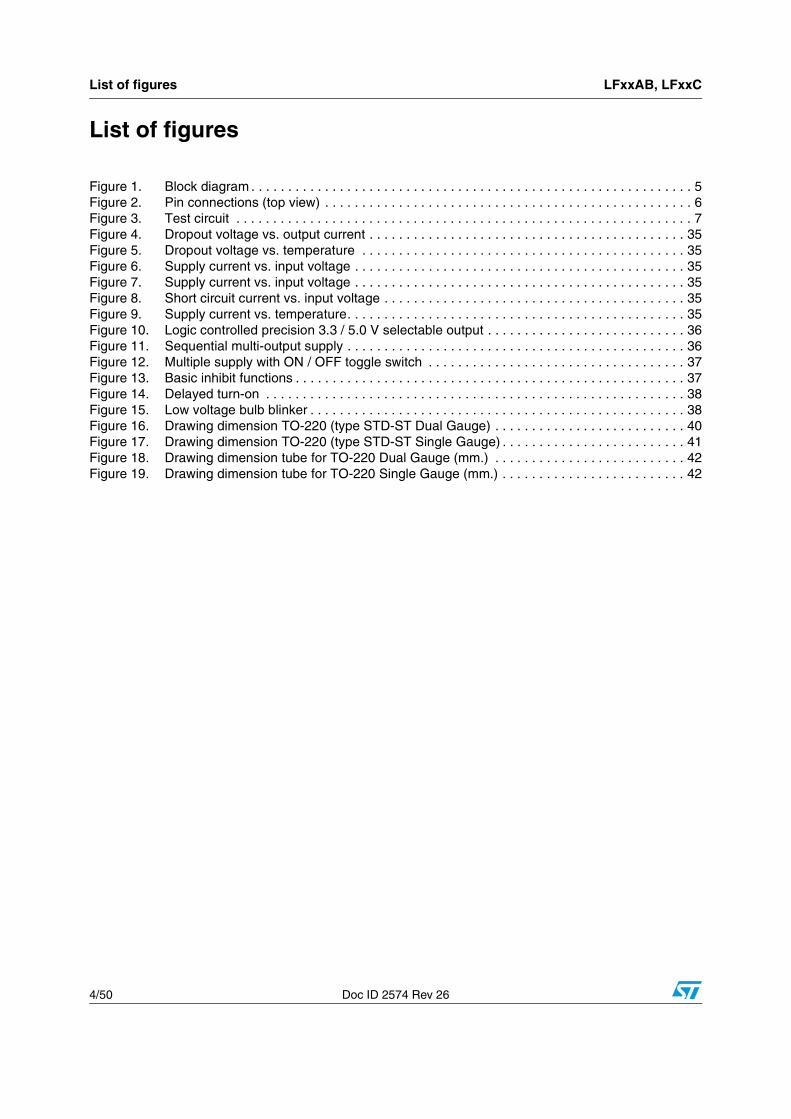
Table 12. Electrical characteristics for LF33AB
Symbol Parameter Test conditions Min. Typ. Max. Unit
VO Output voltageIO = 50 mA, VI = 5.3 V 3.267 3.3 3.333
VIO = 50 mA, VI = 5.3 V, Ta = -25 to 85°C 3.234 3.366
VI Operating input voltage IO = 500 mA 16 V
IO Output current limit 1 A
ΔVO Line regulation VI = 4.3 to 16 V, IO = 5 mA 3 16 mV
ΔVO Load regulation VI = 4.6 V, IO = 5 to 500 mA 3 16 mV
Id Quiescent current
VI = 4.3 to 16V, IO = 0mAON MODE
0.5 1mA
VI = 4.6 to 16V, IO=500mA 12
VI = 6 V OFF MODE 50 100 µA
SVR Supply voltage rejection IO = 5 mA, VI = 5.3 ± 1 V
f = 120 Hz 80
dBf = 1 kHz 75
f = 10 kHz 65
eN Output noise voltage B = 10 Hz to 100 kHz 50 µV
Vd Dropout voltageIO = 200 mA 0.2 0.35
VIO = 500 mA 0.4 0.7
VIL Control input logic low Ta = -40 to 125°C 0.8 V
VIH Control input logic high Ta = -40 to 125°C 2 V
II Control input current VI = 6 V, VC = 6 V 10 µA
COOutput bypass capacitance
ESR = 0.1 to 10 Ω, IO = 0 to 500 mA 2 10 µF

LFxxAB, LFxxC Electrical characteristics
Doc ID 2574 Rev 26 17/50
Refer to the test circuits, TJ = 25 °C, CI = 0.1 µF, CO = 2.2 µF unless otherwise specified.
Table 13. Electrical characteristics for LF33C
Symbol Parameter Test conditions Min. Typ. Max. Unit
VO Output voltageIO = 50 mA, VI = 5.3 V 3.234 3.3 3.366
VIO = 50 mA, VI = 5.3 V, Ta = -25 to 85°C 3.168 3.432
VI Operating input voltage IO = 500 mA 16 V
IO Output current limit 1 A
ΔVO Line regulation VI = 4.3 to 16 V, IO = 5 mA 3 16 mV
ΔVO Load regulation VI = 4.6 V, IO = 5 to 500 mA 3 16 mV
Id Quiescent current
VI = 4.3 to 16V, IO = 0mAON MODE
0.5 1mA
VI = 4.6 to 16V, IO=500mA 12
VI = 6 V OFF MODE 50 100 µA
SVR Supply voltage rejection IO = 5 mA, VI = 5.3 ± 1 V
f = 120 Hz 80
dBf = 1 kHz 75
f = 10 kHz 65
eN Output noise voltage B = 10 Hz to 100 kHz 50 µV
Vd Dropout voltageIO = 200 mA 0.2 0.35
VIO = 500 mA 0.4 0.7
VIL Control input logic low Ta = -40 to 125°C 0.8 V
VIH Control input logic high Ta = -40 to 125°C 2 V
II Control input current VI = 6 V, VC = 6 V 10 µA
COOutput bypass capacitance
ESR = 0.1 to 10 Ω, IO = 0 to 500 mA 2 10 µF

Electrical characteristics LFxxAB, LFxxC
18/50 Doc ID 2574 Rev 26
Refer to the test circuits, TA = -40 to 125°C, CI = 0.1 µF, CO = 2.2 µF unless otherwise specified.
Table 14. Electrical characteristics for LF33CDT-TRY and LF33CPT-TRY (Automotive Grade)
Symbol Parameter Test conditions Min. Typ. Max. Unit
VO Output voltageIO = 50 mA, VI = 5.3 V, Ta = 25°C 3.234 3.3 3.366
VIO = 50 mA, VI = 5.3 V, 3.153 3.447
VI Operating input voltage IO = 500 mA 16 V
IO Output current limit Ta = 25°C 1 A
ΔVO Line regulation VI = 4.3 to 16 V, IO = 5 mA 3 19 mV
ΔVO Load regulation VI = 4.6 V, IO = 5 to 500 mA 3 19 mV
Id Quiescent current
VI = 4.3 to 16V, IO = 0mAON MODE
0.5 2mA
VI = 4.6 to 16V, IO=500mA 12
VI = 6 V OFF MODE 50 120 µA
SVR Supply voltage rejectionIO = 5 mA, VI = 5.3 ± 1 V Ta = 25°C
f = 120 Hz 80
dBf = 1 kHz 75
f = 10 kHz 65
eN Output noise voltage B = 10 Hz to 100 KHz, Ta = 25°C 50 µV
Vd Dropout voltageIO = 200 mA 0.2 1.3
VIO = 500 mA 0.4 1.3
VIL Control input logic low 0.8 V
VIH Control input logic high 2 V
II Control input current VI = 6 V, VC = 6 V, Ta = 25°C 10 µA
COOutput bypass capacitance
ESR = 0.1 to 10 Ω, IO = 0 to 500 mA 2 10 µF

LFxxAB, LFxxC Electrical characteristics
Doc ID 2574 Rev 26 19/50
Refer to the test circuits, TJ = 25 °C, CI = 0.1 µF, CO = 2.2 µF unless otherwise specified.
Table 15. Electrical characteristics for LF50AB
Symbol Parameter Test conditions Min. Typ. Max. Unit
VO Output voltageIO = 50 mA, VI = 7 V 4.95 5 5.05
VIO = 50 mA, VI = 7 V, Ta = -25 to 85°C 4.9 5.1
VI Operating input voltage IO = 500 mA 16 V
IO Output current limit 1 A
ΔVO Line regulation VI = 6 to 16 V, IO = 5 mA 5 25 mV
ΔVO Load regulation VI = 6.3 V, IO = 5 to 500 mA 5 25 mV
Id Quiescent current
VI = 6 to 16V, IO = 0mAON MODE
0.5 1mA
VI = 6.3 to 16V, IO=500mA 12
VI = 6 V OFF MODE 50 100 µA
SVR Supply voltage rejection IO = 5 mA, VI = 7 ± 1 V
f = 120 Hz 76
dBf = 1 kHz 71
f = 10 kHz 60
eN Output noise voltage B = 10 Hz to 100 kHz 50 µV
Vd Dropout voltageIO = 200 mA 0.2 0.35
VIO = 500 mA 0.4 0.7
VIL Control input logic low Ta = -40 to 125°C 0.8 V
VIH Control input logic high Ta = -40 to 125°C 2 V
II Control input current VI = 6 V, VC = 6 V 10 µA
COOutput bypass capacitance
ESR = 0.1 to 10 Ω, IO = 0 to 500 mA 2 10 µF

Electrical characteristics LFxxAB, LFxxC
20/50 Doc ID 2574 Rev 26
Refer to the test circuits, TA = -40 to 125°C, CI = 0.1 µF, CO = 2.2 µF unless otherwise specified.
Table 16. Electrical characteristics for LF50ABDT-TRY (Automotive Grade)
Symbol Parameter Test conditions Min. Typ. Max. Unit
VO Output voltageIO = 50 mA, VI = 7 V, Ta = 25°C 4.95 5 5.05
VIO = 50 mA, VI = 7 V 4.885 5.115
VI Operating input voltage IO = 500 mA 16 V
IO Output current limit Ta = 25°C 1 A
ΔVO Line regulation VI = 6 to 16 V, IO = 5 mA 5 28 mV
ΔVO Load regulation VI = 6.3 V, IO = 5 to 500 mA 5 28 mV
Id Quiescent current
VI = 6 to 16V, IO = 0mAON MODE
0.5 2mA
VI = 6.3 to 16V, IO=500mA 12
VI = 6 V OFF MODE 50 120 µA
SVR Supply voltage rejectionIO = 5 mA, VI = 7 ± 1 V Ta = 25°C
f = 120 Hz 76
dBf = 1 kHz 71
f = 10 kHz 60
eN Output noise voltage B = 10 Hz to 100 kHz, Ta = 25°C 50 µV
Vd Dropout voltageIO = 200 mA 0.2 1.3
VIO = 500 mA 0.4 1.3
VIL Control input logic low 0.8 V
VIH Control input logic high 2 V
II Control input current VI = 6 V, VC = 6 V, Ta = 25°C 10 µA
COOutput bypass capacitance
ESR = 0.1 to 10 Ω, IO = 0 to 500 mA 2 10 µF
LFxxAB, LFxxC Electrical characteristics
Doc ID 2574 Rev 26 21/50
Refer to the test circuits, TJ = 25 °C, CI = 0.1 µF, CO = 2.2 µF unless otherwise specified.
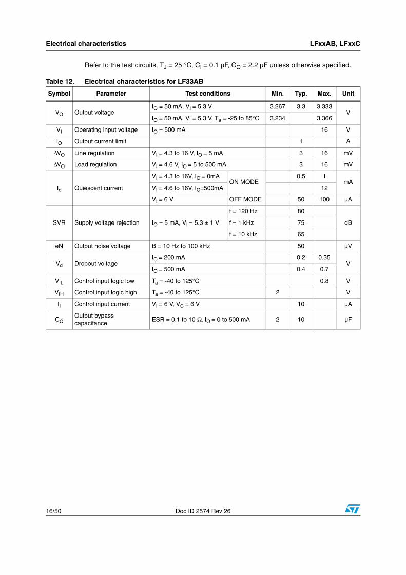
Table 17. Electrical characteristics for LF50C
Symbol Parameter Test conditions Min. Typ. Max. Unit
VO Output voltageIO = 50 mA, VI = 7 V 4.9 5 5.1
VIO = 50 mA, VI = 7 V, Ta = -25 to 85°C 4.8 5.2
VI Operating input voltage IO = 500 mA 16 V
IO Output current limit 1 A
ΔVO Line regulation VI = 6 to 16 V, IO = 5 mA 5 25 mV
ΔVO Load regulation VI = 6.3 V, IO = 5 to 500 mA 5 25 mV
Id Quiescent current
VI = 6 to 16V, IO = 0mAON MODE
0.5 1mA
VI = 6.3 to 16V, IO=500mA 12
VI = 6 V OFF MODE 50 100 µA
SVR Supply voltage rejection IO = 5 mA, VI = 7 ± 1 V
f = 120 Hz 76
dBf = 1 kHz 71
f = 10 kHz 60
eN Output noise voltage B = 10 Hz to 100 kHz 50 µV
Vd Dropout voltageIO = 200 mA 0.2 0.35
VIO = 500 mA 0.4 0.7
VIL Control input logic low Ta = -40 to 125°C 0.8 V
VIH Control input logic high Ta = -40 to 125°C 2 V
II Control input current VI = 6 V, VC = 6 V 10 µA
COOutput bypass capacitance
ESR = 0.1 to 10 Ω, IO = 0 to 500 mA 2 10 µF

Electrical characteristics LFxxAB, LFxxC
22/50 Doc ID 2574 Rev 26
Refer to the test circuits, TA = -40 to 125°C, CI = 0.1 µF, CO = 2.2 µF unless otherwise specified.
Table 18. Electrical characteristics for LF50CDT-TRY and LF50CPT-TRY (Automotive Grade)
Symbol Parameter Test conditions Min. Typ. Max. Unit
VO Output voltageIO = 50 mA, VI = 7 V, Ta = 25°C 4.9 5 5.1
VIO = 50 mA, VI = 7 V 4.785 5.215
VI Operating input voltage IO = 500 mA 16 V
IO Output current limit Ta = 25°C 1 A
ΔVO Line regulation VI = 6 to 16 V, IO = 5 mA 5 28 mV
ΔVO Load regulation VI = 6.3 V, IO = 5 to 500 mA 5 28 mV
Id Quiescent current
VI = 6 to 16V, IO = 0mAON MODE
0.5 2mA
VI = 6.3 to 16V, IO=500mA 12
VI = 6 V OFF MODE 50 120 µA
SVR Supply voltage rejectionIO = 5 mA, VI = 7 ± 1 V Ta = 25°C
f = 120 Hz 76
dBf = 1 kHz 71
f = 10 kHz 60
eN Output noise voltage B = 10 Hz to 100 kHz, Ta = 25°C 50 µV
Vd Dropout voltageIO = 200 mA 0.2 1.3
VIO = 500 mA 0.4 1.3
VIL Control input logic low 0.8 V
VIH Control input logic high 2 V
II Control input current VI = 6 V, VC = 6 V, Ta = 25°C 10 µA
COOutput bypass capacitance
ESR = 0.1 to 10 Ω, IO = 0 to 500 mA 2 10 µF

LFxxAB, LFxxC Electrical characteristics
Doc ID 2574 Rev 26 23/50
Refer to the test circuits, TJ = 25 °C, CI = 0.1 µF, CO = 2.2 µF unless otherwise specified.
Table 19. Electrical characteristics for LF60AB
Symbol Parameter Test conditions Min. Typ. Max. Unit
VO Output voltageIO = 50 mA, VI = 8 V 5.94 6 6.06
VIO = 50 mA, VI = 8 V, Ta = -25 to 85°C 5.88 6.12
VI Operating input voltage IO = 500 mA 16 V
IO Output current limit 1 A
ΔVO Line regulation VI = 7 to 16 V, IO = 5 mA 6 30 mV
ΔVO Load regulation VI = 7.3 V, IO = 5 to 500 mA 6 30 mV
Id Quiescent current
VI = 7 to 16V, IO = 0mAON MODE
0.7 1.5mA
VI = 7.3 to 16V, IO=500mA 12
VI = 9 V OFF MODE 70 140 µA
SVR Supply voltage rejection IO = 5 mA, VI = 8 ± 1 V
f = 120 Hz 75
dBf = 1 kHz 70
f = 10 kHz 60
eN Output noise voltage B = 10 Hz to 100 kHz 50 µV
Vd Dropout voltageIO = 200 mA 0.2 0.35
VIO = 500 mA 0.4 0.7
VIL Control input logic low Ta = -40 to 125°C 0.8 V
VIH Control input logic high Ta = -40 to 125°C 2 V
II Control input current VI = 9 V, VC = 6 V 10 µA
COOutput bypass capacitance
ESR = 0.1 to 10 Ω, IO = 0 to 500 mA 2 10 µF

Electrical characteristics LFxxAB, LFxxC
24/50 Doc ID 2574 Rev 26
Refer to the test circuits, TJ = 25 °C, CI = 0.1 µF, CO = 2.2 µF unless otherwise specified.
Table 20. Electrical characteristics for LF60C
Symbol Parameter Test conditions Min. Typ. Max. Unit
VO Output voltageIO = 50 mA, VI = 8 V 5.88 6 6.12
VIO = 50 mA, VI = 8 V, Ta = -25 to 85°C 5.76 6.24
VI Operating input voltage IO = 500 mA 16 V
IO Output current limit 1 A
ΔVO Line regulation VI = 7 to 16 V, IO = 5 mA 6 30 mV
ΔVO Load regulation VI = 7.3 V, IO = 5 to 500 mA 6 30 mV
Id Quiescent current
VI = 7 to 16V, IO = 0mAON MODE
0.7 1.5mA
VI = 7.3 to 16V, IO=500mA 12
VI = 9 V OFF MODE 70 140 µA
SVR Supply voltage rejection IO = 5 mA, VI = 8 ± 1 V
f = 120 Hz 75
dBf = 1 kHz 70
f = 10 kHz 60
eN Output noise voltage B = 10 Hz to 100 kHz 50 µV
Vd Dropout voltageIO = 200 mA 0.2 0.35
VIO = 500 mA 0.4 0.7
VIL Control input logic low Ta = -40 to 125°C 0.8 V
VIH Control input logic high Ta = -40 to 125°C 2 V
II Control input current VI = 9 V, VC = 6 V 10 µA
COOutput bypass capacitance
ESR = 0.1 to 10 Ω, IO = 0 to 500 mA 2 10 µF

LFxxAB, LFxxC Electrical characteristics
Doc ID 2574 Rev 26 25/50
Refer to the test circuits, TJ = 25 °C, CI = 0.1 µF, CO = 2.2 µF unless otherwise specified.
Table 21. Electrical characteristics for LF80AB
Symbol Parameter Test conditions Min. Typ. Max. Unit
VO Output voltageIO = 50 mA, VI = 10 V 7.92 8 8.08
VIO = 50 mA, VI = 10 V, Ta = -25 to 85°C 7.84 8.16
VI Operating input voltage IO = 500 mA 16 V
IO Output current limit 1 A
ΔVO Line regulation VI = 9 to 16 V, IO = 5 mA 8 40 mV
ΔVO Load regulation VI = 9.3 V, IO = 5 to 500 mA 8 40 mV
Id Quiescent current
VI = 9 to 16V, IO = 0mAON MODE
0.7 1.5mA
VI = 9.3 to 16V, IO=500mA 12
VI = 9 V OFF MODE 70 140 µA
SVR Supply voltage rejection IO = 5 mA, VI = 10 ± 1 V
f = 120 Hz 72
dBf = 1 kHz 67
f = 10 kHz 57
eN Output noise voltage B = 10 Hz to 100 kHz 50 µV
Vd Dropout voltageIO = 200 mA 0.2 0.35
VIO = 500 mA 0.4 0.7
VIL Control input logic low Ta = -40 to 125°C 0.8 V
VIH Control input logic high Ta = -40 to 125°C 2 V
II Control input current VI = 9 V, VC = 6 V 10 µA
COOutput bypass capacitance
ESR = 0.1 to 10 Ω, IO = 0 to 500 mA 2 10 µF

Electrical characteristics LFxxAB, LFxxC
26/50 Doc ID 2574 Rev 26
Refer to the test circuits, TJ = 25 °C, CI = 0.1 µF, CO = 2.2 µF unless otherwise specified.
Table 22. Electrical characteristics for LF80C
Symbol Parameter Test conditions Min. Typ. Max. Unit
VO Output voltageIO = 50 mA, VI = 10 V 7.84 8 8.16
VIO = 50 mA, VI = 10 V, Ta = -25 to 85°C 7.68 8.32
VI Operating input voltage IO = 500 mA 16 V
IO Output current limit 1 A
ΔVO Line regulation VI = 9 to 16 V, IO = 5 mA 8 40 mV
ΔVO Load regulation VI = 9.3 V, IO = 5 to 500 mA 8 40 mV
Id Quiescent current
VI = 9 to 16V, IO = 0mAON MODE
0.7 1.5mA
VI = 9.3 to 16V, IO=500mA 12
VI = 9 V OFF MODE 70 140 µA
SVR Supply voltage rejection IO = 5 mA, VI = 10 ± 1 V
f = 120 Hz 72
dBf = 1 kHz 67
f = 10 kHz 57
eN Output noise voltage B = 10 Hz to 100 kHz 50 µV
Vd Dropout voltageIO = 200 mA 0.2 0.35
VIO = 500 mA 0.4 0.7
VIL Control input logic low Ta = -40 to 125°C 0.8 V
VIH Control input logic high Ta = -40 to 125°C 2 V
II Control input current VI = 9 V, VC = 6 V 10 µA
COOutput bypass capacitance
ESR = 0.1 to 10 Ω, IO = 0 to 500 mA 2 10 µF

LFxxAB, LFxxC Electrical characteristics
Doc ID 2574 Rev 26 27/50
Refer to the test circuits, TA = -40 to 125°C, CI = 0.1 µF, CO = 2.2 µF unless otherwise specified.
Table 23. Electrical characteristics for LF80CDT-TRY (Automotive Grade)
Symbol Parameter Test conditions Min. Typ. Max. Unit
VO Output voltageIO = 50 mA, VI = 10 V, Ta = 25°C 7.84 8 8.16
VIO = 50 mA, VI = 10 V 7.665 8.335
VI Operating input voltage IO = 500 mA 16 V
IO Output current limit Ta = 25°C 1 A
ΔVO Line regulation VI = 9 to 16 V, IO = 5 mA 8 44 mV
ΔVO Load regulation VI = 9.3 V, IO = 5 to 500 mA 8 44 mV
Id Quiescent current
VI = 9 to 16V, IO = 0mAON MODE
0.7 2.5mA
VI = 9.3 to 16V, IO=500mA 12
VI = 9 V OFF MODE 70 160 µA
SVR Supply voltage rejectionIO = 5 mA, VI = 10 ± 1 VTa = 25°C
f = 120 Hz 72
dBf = 1 kHz 67
f = 10 kHz 57
eN Output noise voltage B = 10 Hz to 100 kHz, Ta = 25°C 50 µV
Vd Dropout voltageIO = 200 mA 0.2 1.3
VIO = 500 mA 0.4 1.3
VIL Control input logic low 0.8 V
VIH Control input logic high 2 V
II Control input current VI = 9 V, VC = 6 V, Ta = 25°C 10 µA
COOutput bypass capacitance
ESR = 0.1 to 10 Ω, IO = 0 to 500 mA 2 10 µF

Electrical characteristics LFxxAB, LFxxC
28/50 Doc ID 2574 Rev 26
Refer to the test circuits, TJ = 25 °C, CI = 0.1 µF, CO = 2.2 µF unless otherwise specified.
Table 24. Electrical characteristics for LF85AB
Symbol Parameter Test conditions Min. Typ. Max. Unit
VO Output voltageIO = 50 mA, VI = 10.5 V 8.415 8.5 8.585
VIO = 50 mA, VI = 10.5 V, Ta = -25 to 85°C 8.33 8.67
VI Operating input voltage IO = 500 mA 16 V
IO Output current limit 1 A
ΔVO Line regulation VI = 9.5 to 16 V, IO = 5 mA 8 42 mV
ΔVO Load regulation VI = 9.8 V, IO = 5 to 500 mA 8 42 mV
Id Quiescent current
VI = 9.5 to 16V, IO = 0mAON MODE
0.7 1.5mA
VI = 9.8 to 16V, IO=500mA 12
VI = 9 V OFF MODE 70 140 µA
SVR Supply voltage rejection IO = 5 mA, VI = 10.5 ± 1 V
f = 120 Hz 72
dBf = 1 kHz 67
f = 10 kHz 57
eN Output noise voltage B = 10 Hz to 100 kHz 50 µV
Vd Dropout voltageIO = 200 mA 0.2 0.35
VIO = 500 mA 0.4 0.7
VIL Control input logic low Ta = -40 to 125°C 0.8 V
VIH Control input logic high Ta = -40 to 125°C 2 V
II Control input current VI = 9 V, VC = 6 V 10 µA
COOutput bypass capacitance
ESR = 0.1 to 10 Ω, IO = 0 to 500 mA 2 10 µF

LFxxAB, LFxxC Electrical characteristics
Doc ID 2574 Rev 26 29/50
Refer to the test circuits, TJ = 25 °C, CI = 0.1 µF, CO = 2.2 µF unless otherwise specified.
Table 25. Electrical characteristics for LF85C
Symbol Parameter Test conditions Min. Typ. Max. Unit
VO Output voltageIO = 50 mA, VI = 10.5 V 8.33 8.5 8.67
VIO = 50 mA, VI = 10.5 V, Ta = -25 to 85°C 8.16 8.84
VI Operating input voltage IO = 500 mA 16 V
IO Output current limit 1 A
ΔVO Line regulation VI = 9.5 to 16 V, IO = 5 mA 8 42 mV
ΔVO Load regulation VI = 9.8 V, IO = 5 to 500 mA 8 42 mV
Id Quiescent current
VI = 9.5 to 16V, IO = 0mAON MODE
0.7 1.5mA
VI = 9.8 to 16V, IO=500mA 12
VI = 9 V OFF MODE 70 140 µA
SVR Supply voltage rejection IO = 5 mA, VI = 10.5 ± 1 V
f = 120 Hz 72
dBf = 1 kHz 67
f = 10 kHz 57
eN Output noise voltage B = 10 Hz to 100 kHz 50 µV
Vd Dropout voltageIO = 200 mA 0.2 0.35
VIO = 500 mA 0.4 0.7
VIL Control input logic low Ta = -40 to 125°C 0.8 V
VIH Control input logic high Ta = -40 to 125°C 2 V
II Control input current VI = 9 V, VC = 6 V 10 µA
COOutput bypass capacitance
ESR = 0.1 to 10 Ω, IO = 0 to 500 mA 2 10 µF

Electrical characteristics LFxxAB, LFxxC
30/50 Doc ID 2574 Rev 26
Refer to the test circuits, TA = -40 to 25°C, CI = 0.1 µF, CO = 2.2 µF unless otherwise specified.
Table 26. Electrical characteristics for LF85CDT-TRY and LF85CPT-TRY (Automotive Grade)
Symbol Parameter Test conditions Min. Typ. Max. Unit
VO Output voltageIO = 50 mA, VI = 10.5 V, Ta = 25°C 8.33 8.5 8.67
VIO = 50 mA, VI = 10.5 V 8.145 8.855
VI Operating input voltage IO = 500 mA 16 V
IO Output current limit Ta = 25°C 1 A
ΔVO Line regulation VI = 9.5 to 16 V, IO = 5 mA 8 44 mV
ΔVO Load regulation VI = 9.8 V, IO = 5 to 500 mA 8 44 mV
Id Quiescent current
VI = 9.5 to 16V, IO = 0mAON MODE
0.7 2.5mA
VI = 9.8 to 16V, IO=500mA 12
VI = 9 V OFF MODE 70 160 µA
SVR Supply voltage rejectionIO = 5 mA, VI = 10.5 ± 1 VTa = 25°C
f = 120 Hz 72
dBf = 1 kHz 67
f = 10 kHz 57
eN Output noise voltage B = 10 Hz to 100 kHz, Ta = 25°C 50 µV
Vd Dropout voltageIO = 200 mA 0.2 1.3
VIO = 500 mA 0.4 1.3
VIL Control input logic low 0.8 V
VIH Control input logic high 2 V
II Control input current VI = 9 V, VC = 6 V, Ta = 25°C 10 µA
COOutput bypass capacitance
ESR = 0.1 to 10 Ω, IO = 0 to 500 mA 2 10 µF
LFxxAB, LFxxC Electrical characteristics
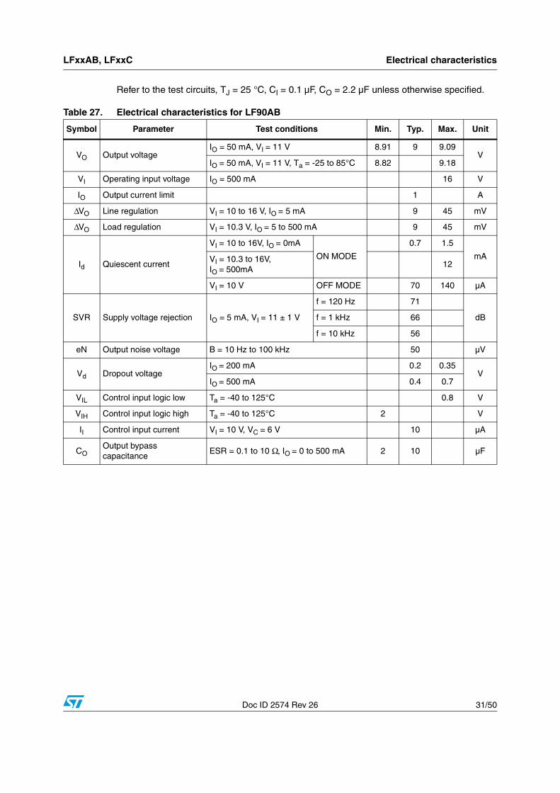
Doc ID 2574 Rev 26 31/50
Refer to the test circuits, TJ = 25 °C, CI = 0.1 µF, CO = 2.2 µF unless otherwise specified.
Table 27. Electrical characteristics for LF90AB
Symbol Parameter Test conditions Min. Typ. Max. Unit
VO Output voltageIO = 50 mA, VI = 11 V 8.91 9 9.09
VIO = 50 mA, VI = 11 V, Ta = -25 to 85°C 8.82 9.18
VI Operating input voltage IO = 500 mA 16 V
IO Output current limit 1 A
ΔVO Line regulation VI = 10 to 16 V, IO = 5 mA 9 45 mV
ΔVO Load regulation VI = 10.3 V, IO = 5 to 500 mA 9 45 mV
Id Quiescent current
VI = 10 to 16V, IO = 0mA
ON MODE
0.7 1.5
mAVI = 10.3 to 16V, IO = 500mA
12
VI = 10 V OFF MODE 70 140 µA
SVR Supply voltage rejection IO = 5 mA, VI = 11 ± 1 V
f = 120 Hz 71
dBf = 1 kHz 66
f = 10 kHz 56
eN Output noise voltage B = 10 Hz to 100 kHz 50 µV
Vd Dropout voltageIO = 200 mA 0.2 0.35
VIO = 500 mA 0.4 0.7
VIL Control input logic low Ta = -40 to 125°C 0.8 V
VIH Control input logic high Ta = -40 to 125°C 2 V
II Control input current VI = 10 V, VC = 6 V 10 µA
COOutput bypass capacitance
ESR = 0.1 to 10 Ω, IO = 0 to 500 mA 2 10 µF

Electrical characteristics LFxxAB, LFxxC
32/50 Doc ID 2574 Rev 26
Refer to the test circuits, TJ = 25 °C, CI = 0.1 µF, CO = 2.2 µF unless otherwise specified.
Table 28. Electrical characteristics for LF90C
Symbol Parameter Test conditions Min. Typ. Max. Unit
VO Output voltageIO = 50 mA, VI = 11 V 8.82 9 9.18
VIO = 50 mA, VI = 11 V, Ta = -25 to 85°C 8.64 9.36
VI Operating input voltage IO = 500 mA 16 V
IO Output current limit 1 A
ΔVO Line regulation VI = 10 to 16 V, IO = 5 mA 9 45 mV
ΔVO Load regulation VI = 10.3 V, IO = 5 to 500 mA 9 45 mV
Id Quiescent current
VI = 10 to 16V, IO = 0mA
ON MODE
0.7 1.5
mAVI = 10.3 to 16V,IO = 500mA
12
VI = 10 V OFF MODE 70 140 µA
SVR Supply voltage rejection IO = 5 mA, VI = 11 ± 1 V
f = 120 Hz 71
dBf = 1 kHz 66
f = 10 kHz 56
eN Output noise voltage B = 10 Hz to 100 kHz 50 µV
Vd Dropout voltageIO = 200 mA 0.2 0.35
VIO = 500 mA 0.4 0.7
VIL Control input logic low Ta = -40 to 125°C 0.8 V
VIH Control input logic high Ta = -40 to 125°C 2 V
II Control input current VI = 10 V, VC = 6 V 10 µA
COOutput bypass capacitance
ESR = 0.1 to 10 Ω, IO = 0 to 500 mA 2 10 µF

LFxxAB, LFxxC Electrical characteristics
Doc ID 2574 Rev 26 33/50
Refer to the test circuits, TJ = 25 °C, CI = 0.1 µF, CO = 2.2 µF unless otherwise specified.
Table 29. Electrical characteristics for LF120AB
Symbol Parameter Test conditions Min. Typ. Max. Unit
VO Output voltageIO = 50 mA, VI = 15 V 11.88 12 12.12
VIO = 50 mA, VI = 15 V, Ta = -25 to 85°C 11.76 12.24
VI Operating input voltage IO = 500 mA 16 V
IO Output current limit 1 A
ΔVO Line regulation VI = 13 to 16 V, IO = 5 mA 12 60 mV
ΔVO Load regulation VI = 13.3 V, IO = 5 to 500 mA 12 60 mV
Id Quiescent current
VI = 13 to 16V, IO = 0mA
ON MODE
0.7 1.5
mAVI = 13.3 to 16V,IO = 500mA
12
VI = 13 V OFF MODE 70 140 µA
SVR Supply voltage rejection IO = 5 mA, VI = 14 ± 1 V
f = 120 Hz 69
dBf = 1 kHz 64
f = 10 kHz 54
eN Output noise voltage B = 10 Hz to 100 kHz 50 µV
Vd Dropout voltageIO = 200 mA 0.2 0.35
VIO = 500 mA 0.4 0.7
VIL Control input logic low Ta = -40 to 125°C 0.8 V
VIH Control input logic high Ta = -40 to 125°C 2 V
II Control input current VI = 13 V, VC = 6 V 10 µA
COOutput bypass capacitance
ESR = 0.1 to 10 Ω, IO = 0 to 500 mA 2 10 µF

Electrical characteristics LFxxAB, LFxxC
34/50 Doc ID 2574 Rev 26
Refer to the test circuits, TJ = 25 °C, CI = 0.1 µF, CO = 2.2 µF unless otherwise specified.
Table 30. Electrical characteristics for LF120C
Symbol Parameter Test conditions Min. Typ. Max. Unit
VO Output voltageIO = 50 mA, VI = 14 V 11.76 12 12.24
VIO = 50 mA, VI = 14 V, Ta = -25 to 85°C 11.52 12.48
VI Operating input voltage IO = 500 mA 16 V
IO Output current limit 1 A
ΔVO Line regulation VI = 13 to 16 V, IO = 5 mA 12 60 mV
ΔVO Load regulation VI = 13.3 V, IO = 5 to 500 mA 12 60 mV
Id Quiescent current
VI = 13 to 16V, IO = 0mA
ON MODE
0.7 1.5
mAVI = 13.3 to 16V,IO = 500mA
12
VI = 13 V OFF MODE 70 140 µA
SVR Supply voltage rejection IO = 5 mA, VI = 14 ± 1 V
f = 120 Hz 69
dBf = 1 kHz 64
f = 10 kHz 54
eN Output noise voltage B = 10 Hz to 100 kHz 50 µV
Vd Dropout voltageIO = 200 mA 0.2 0.35
VIO = 500 mA 0.4 0.7
VIL Control input logic low Ta = -40 to 125°C 0.8 V
VIH Control input logic high Ta = -40 to 125°C 2 V
II Control input current VI = 13 V, VC = 6 V 10 µA
COOutput bypass capacitance
ESR = 0.1 to 10 Ω, IO = 0 to 500 mA 2 10 µF

LFxxAB, LFxxC Typical performance characteristics
Doc ID 2574 Rev 26 35/50
5 Typical performance characteristics
Unless otherwise specified VO(NOM) = 3.3 V.Figure 4. Dropout voltage vs. output current Figure 5. Dropout voltage vs. temperature
Figure 6. Supply current vs. input voltage Figure 7. Supply current vs. input voltage
Figure 8. Short circuit current vs. input voltage
Figure 9. Supply current vs. temperature

Typical performance characteristics LFxxAB, LFxxC
36/50 Doc ID 2574 Rev 26
Figure 10. Logic controlled precision 3.3 / 5.0 V selectable output
Figure 11. Sequential multi-output supply

LFxxAB, LFxxC Typical performance characteristics
Doc ID 2574 Rev 26 37/50
Figure 12. Multiple supply with ON / OFF toggle switch
Figure 13. Basic inhibit functions

Typical performance characteristics LFxxAB, LFxxC
38/50 Doc ID 2574 Rev 26
Figure 14. Delayed turn-on
Figure 15. Low voltage bulb blinker

LFxxAB, LFxxC Package mechanical data
Doc ID 2574 Rev 26 39/50
6 Package mechanical data
In order to meet environmental requirements, ST offers these devices in different grades of ECOPACK® packages, depending on their level of environmental compliance. ECOPACK® specifications, grade definitions and product status are available at: www.st.com. ECOPACK® is an ST trademark.
In spite of some difference in tolerances, the packages are compatible.
Table 31. TO-220 mechanical data
Dim.
Type STD - ST Dual Gauge Type STD - ST Single Gauge
mm. mm.
Min. Typ. Max. Min. Typ. Max.
A 4.40 4.60 4.40 4.60
b 0.61 0.88 0.61 0.88
b1 1.14 1.70 1.14 1.70
c 0.48 0.70 0.48 0.70
D 15.25 15.75 15.25 15.75
D1 1.27
E 10.00 10.40 10.00 10.40
e 2.40 2.70 2.40 2.70
e1 4.95 5.15 4.95 5.15
F 1.23 1.32 0.51 0.60
H1 6.20 6.60 6.20 6.60
J1 2.40 2.72 2.40 2.72
L 13.00 14.00 13.00 14.00
L1 3.50 3.93 3.50 3.93
L20 16.40 16.40
L30 28.90 28.90
∅P 3.75 3.85 3.75 3.85
Q 2.65 2.95 2.65 2.95

Package mechanical data LFxxAB, LFxxC
40/50 Doc ID 2574 Rev 26
Note: 1 Maximum resin gate protrusion: 0.5 mm.
2 Resin gate position is accepted in each of the two positions shown on the drawing, or their symmetrical.
Figure 16. Drawing dimension TO-220 (type STD-ST Dual Gauge)
0015988_S

LFxxAB, LFxxC Package mechanical data
Doc ID 2574 Rev 26 41/50
Figure 17. Drawing dimension TO-220 (type STD-ST Single Gauge)
8174627_B

Package mechanical data LFxxAB, LFxxC
42/50 Doc ID 2574 Rev 26
Figure 18. Drawing dimension tube for TO-220 Dual Gauge (mm.)
Figure 19. Drawing dimension tube for TO-220 Single Gauge (mm.)

LFxxAB, LFxxC Package mechanical data
Doc ID 2574 Rev 26 43/50
Dim.mm. inch.
Min. Typ. Max. Min. Typ. Max.A 4.8 0.189C 1.37 0.054D 2.4 2.8 0.094 0.110D1 1.2 1.35 0.047 0.053E 0.35 0.55 0.014 0.022F 0.8 1.05 0.031 0.041F1 1 1.4 0.039 0.055G 3.2 3.4 3.6 0.126 0.134 0.142
G1 6.6 6.8 7 0.260 0.268 0.276H2 10.4 0.409H3 10.05 10.4 0.396 0.409L 17.85 0.703L1 15.75 0.620L2 21.4 0.843L3 22.5 0.886L5 2.6 3 0.102 0.118L6 15.1 15.8 0.594 0.622L7 6 6.6 0.236 0.260M 4.5 0.177
M1 4 0.157Dia1 3.65 3.85 0.144 0.152
PENTAWATT (Vertical) mechanical data
P010E

Package mechanical data LFxxAB, LFxxC
44/50 Doc ID 2574 Rev 26
Dim.mm. inch.
Min. Typ Max. Min. Typ. Max.
A 4.40 4.60 0.173 0.181
B 2.5 2.7 0.098 0.106
D 2.5 2.75 0.098 0.108
E 0.45 0.70 0.017 0.027
F 0.75 1 0.030 0.039
F1 1.15 1.50 0.045 0.059
F2 1.15 1.50 0.045 0.059
G 4.95 5.2 0.194 0.204
G1 2.4 2.7 0.094 0.106
H 10.0 10.40 0.393 0.409
L2 16 0.630
L3 28.6 30.6 1.126 1.204
L4 9.8 10.6 0.385 0.417
L5 2.9 3.6 0.114 0.142
L6 15.9 16.4 0.626 0.645
L7 9 9.3 0.354 0.366
DIA. 3 3.2 0.118 0.126
TO-220FP mechanical data
7012510A-H

LFxxAB, LFxxC Package mechanical data
Doc ID 2574 Rev 26 45/50
Dim.mm. inch.
Min. Typ. Max. Min. Typ. Max.
A 2.2 2.4 0.086 0.094
A1 0.9 1.1 0.035 0.043
A2 0.03 0.23 0.001 0.009
B 0.64 0.9 0.025 0.035
b4 5.2 5.4 0.204 0.212
C 0.45 0.6 0.017 0.023
C2 0.48 0.6 0.019 0.023
D 6 6.2 0.236 0.244
D1 5.1 0.200
E 6.4 6.6 0.252 0.260
E1 4.7 0.185
e 2.28 0.090
e1 4.4 4.6 0.173 0.181
H 9.35 10.1 0.368 0.397
L 1 0.039
(L1) 2.8 0.110
L2 0.8 0.031
L4 0.6 1 0.023 0.039
R 0.2 0.008
V2 0° 8° 0° 8°
DPAK mechanical data
0068772-F

Package mechanical data LFxxAB, LFxxC
46/50 Doc ID 2574 Rev 26
Dim.mm. inch.
Min. Typ. Max. Min. Typ. Max.
A 2.2 2.4 0.086 0.094
A1 0.9 1.1 0.035 0.043
A2 0.03 0.23 0.001 0.009
B 0.4 0.6 0.015 0.023
B2 5.2 5.4 0.204 0.212
C 0.45 0.6 0.017 0.023
C2 0.48 0.6 0.019 0.023
D 6 6.2 0.236 0.244
D1 5.1 0.201
E 6.4 6.6 0.252 0.260
E1 4.7 0.185
e 1.27 0.050
G 4.9 5.25 0.193 0.206
G1 2.38 2.7 0.093 0.106
H 9.35 10.1 0.368 0.397
L2 0.8 1 0.031 0.039
L4 0.6 1 0.023 0.039
L5 1 0.039
L6 2.8 0.110
PPAK mechanical data
0078180-E

LFxxAB, LFxxC Package mechanical data
Doc ID 2574 Rev 26 47/50
Dim.mm. inch.
Min. Typ. Max. Min. Typ. Max.
A 330 12.992
C 12.8 13.0 13.2 0.504 0.512 0.519
D 20.2 0.795
N 60 2.362
T 22.4 0.882
Ao 6.80 6.90 7.00 0.268 0.272 0.2.76
Bo 10.40 10.50 10.60 0.409 0.413 0.417
Ko 2.55 2.65 2.75 0.100 0.104 0.105
Po 3.9 4.0 4.1 0.153 0.157 0.161
P 7.9 8.0 8.1 0.311 0.315 0.319
Tape & reel DPAK-PPAK mechanical data

Order codes LFxxAB, LFxxC
48/50 Doc ID 2574 Rev 26
7 Order codes
Table 32. Order codes
Packages Output voltagesTO-220 TO-220FP DPAK (tape and reel) PPAK PPAK (tape and reel)
LF15ABV (1)
1. Available on request.
LF15ABP (1) LF15ABDT-TR LF15ABPT (1) 1.5 V
LF18CP(1) LF18CDT-TR LF18CPT-TR 1.8 V
LF18CDT-TRY (2)
2. Automotive Grade products.
1.8 V
LF18ABP (1) LF18ABDT-TR LF18ABPT-TR 1.8 V
LF25CP (1) LF25CDT-TR LF25CPT-TR 2.5 V
LF25CDT-TRY (2) 2.5 V
LF25ABP (1) LF25ABDT-TR LF25ABPT (1) 2.5 V
LF25ABDT-TRY (2) 2.5 V
LF33CV LF33CDT-TR LF33CPT-TR 3.3 V
LF33CV-DG (3)
3. TO-220 Dual Gauge frame.
LF33CDT-TRY (2) LF33CPT-TRY (2) 3.3 V
LF33ABV LF33ABDT-TR 3.3 V
LF33ABV-DG (3) 3.3 V
LF50CV LF50CDT-TR LF50CPT-TR 5 V
LF50CDT-TRY (2) LF50CPT-TRY (2) 5 V
LF50ABV LF50ABP LF50ABDT-TR LF50ABPT-TR 5 V
LF50ABV-DG (3) 5 V
LF50ABDT-TRY (2) 5 V
LF60CV LF60CP (1) LF60CDT-TR LF60CPT-TR (1) 6 V
LF60ABV LF60ABP (1) LF60ABDT-TR LF60ABPT (1) LF60ABPT-TR (1) 6 V
LF80CV LF80CP (1) LF80CDT-TR 8 V
LF80CDT-TRY (2) 8 V
LF80ABV LF80ABP (1) LF80ABDT-TR 8 V
LF85CDT-TR LF85CPT-TR 8.5 V
LF85CDT-TRY (2) LF85CPT-TRY (2) 8.5 V
LF90CV LF90CP (1) LF90CPT-TR 9 V
LF120CP (1) LF120CDT-TR 12 V
LF120ABV LF120ABDT-TR LF120ABPT (1) 12 V

LFxxAB, LFxxC Revision history
Doc ID 2574 Rev 26 49/50
8 Revision history
Table 33. Document revision history
Date Revision Changes
21-Jun-2004 14 Document updating.
24-May-2006 15 Order codes updated.
02-Apr-2007 16 Order codes updated.
14-May-2007 17 Order codes updated.
26-Jul-2007 18 Add Table 1 in cover page.
26-Nov-2007 19 Modified: Table 32.
16-Jan-2008 20Added new order codes for Automotive grade products see Table 32 on page 48.
12-Feb-2008 21 Modified: Table 32 on page 48.
10-Jul-2008 22 Modified: Table 32 on page 48.
05-May-2010 23Added: Table 31 on page 39, Figure 16 on page 40, Figure 17 on page 41, Figure 18 and Figure 19 on page 42.
16-Nov-2010 24 Modified: RthJC value for TO-220 Table 3 on page 7.
10-Feb-2012 25 Added: order code LF33CV-DG and LF33ABV-DG Table 32 on page 48.
09-Mar-2012 26 Added: order code LF50ABV-DG Table 32 on page 48.

LFxxAB, LFxxC
50/50 Doc ID 2574 Rev 26
Please Read Carefully:
Information in this document is provided solely in connection with ST products. STMicroelectronics NV and its subsidiaries (“ST”) reserve theright to make changes, corrections, modifications or improvements, to this document, and the products and services described herein at anytime, without notice.
All ST products are sold pursuant to ST’s terms and conditions of sale.
Purchasers are solely responsible for the choice, selection and use of the ST products and services described herein, and ST assumes noliability whatsoever relating to the choice, selection or use of the ST products and services described herein.
No license, express or implied, by estoppel or otherwise, to any intellectual property rights is granted under this document. If any part of thisdocument refers to any third party products or services it shall not be deemed a license grant by ST for the use of such third party productsor services, or any intellectual property contained therein or considered as a warranty covering the use in any manner whatsoever of suchthird party products or services or any intellectual property contained therein.
UNLESS OTHERWISE SET FORTH IN ST’S TERMS AND CONDITIONS OF SALE ST DISCLAIMS ANY EXPRESS OR IMPLIEDWARRANTY WITH RESPECT TO THE USE AND/OR SALE OF ST PRODUCTS INCLUDING WITHOUT LIMITATION IMPLIEDWARRANTIES OF MERCHANTABILITY, FITNESS FOR A PARTICULAR PURPOSE (AND THEIR EQUIVALENTS UNDER THE LAWSOF ANY JURISDICTION), OR INFRINGEMENT OF ANY PATENT, COPYRIGHT OR OTHER INTELLECTUAL PROPERTY RIGHT.
UNLESS EXPRESSLY APPROVED IN WRITING BY TWO AUTHORIZED ST REPRESENTATIVES, ST PRODUCTS ARE NOTRECOMMENDED, AUTHORIZED OR WARRANTED FOR USE IN MILITARY, AIR CRAFT, SPACE, LIFE SAVING, OR LIFE SUSTAININGAPPLICATIONS, NOR IN PRODUCTS OR SYSTEMS WHERE FAILURE OR MALFUNCTION MAY RESULT IN PERSONAL INJURY,DEATH, OR SEVERE PROPERTY OR ENVIRONMENTAL DAMAGE. ST PRODUCTS WHICH ARE NOT SPECIFIED AS "AUTOMOTIVEGRADE" MAY ONLY BE USED IN AUTOMOTIVE APPLICATIONS AT USER’S OWN RISK.
Resale of ST products with provisions different from the statements and/or technical features set forth in this document shall immediately voidany warranty granted by ST for the ST product or service described herein and shall not create or extend in any manner whatsoever, anyliability of ST.
ST and the ST logo are trademarks or registered trademarks of ST in various countries.
Information in this document supersedes and replaces all information previously supplied.
The ST logo is a registered trademark of STMicroelectronics. All other names are the property of their respective owners.
© 2012 STMicroelectronics - All rights reserved
STMicroelectronics group of companies
Australia - Belgium - Brazil - Canada - China - Czech Republic - Finland - France - Germany - Hong Kong - India - Israel - Italy - Japan - Malaysia - Malta - Morocco - Philippines - Singapore - Spain - Sweden - Switzerland - United Kingdom - United States of America
www.st.com
![Isoflavonoids from Crotalaria albida Inhibit Adipocyte ...€¦ · germacranolidecompounds[18]thatpresent PPAR-γantagonismeffectshavebeenshownto inhibit adipocytedifferentiationandlipidaccumulationin](https://img.pdfslide.net/doc/110x75/5f4dcbe6465a9b47ae7bbf0a/isoflavonoids-from-crotalaria-albida-inhibit-adipocyte-germacranolidecompounds18thatpresent.jpg)