Embed Size (px)
Citation preview

Vivado Design Suite UserGuide
Programming and Debugging
UG908 (v2021.1) June 16, 2021
See all versionsof this document
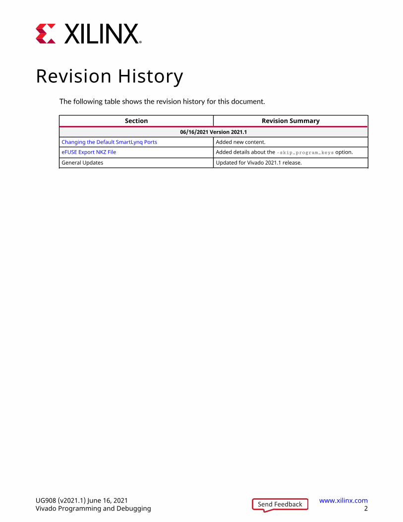
Revision HistoryThe following table shows the revision history for this document.
Section Revision Summary06/16/2021 Version 2021.1
Changing the Default SmartLynq Ports Added new content.
eFUSE Export NKZ File Added details about the -skip_program_keys option.
General Updates Updated for Vivado 2021.1 release.
Revision History
UG908 (v2021.1) June 16, 2021 www.xilinx.comVivado Programming and Debugging 2Send Feedback
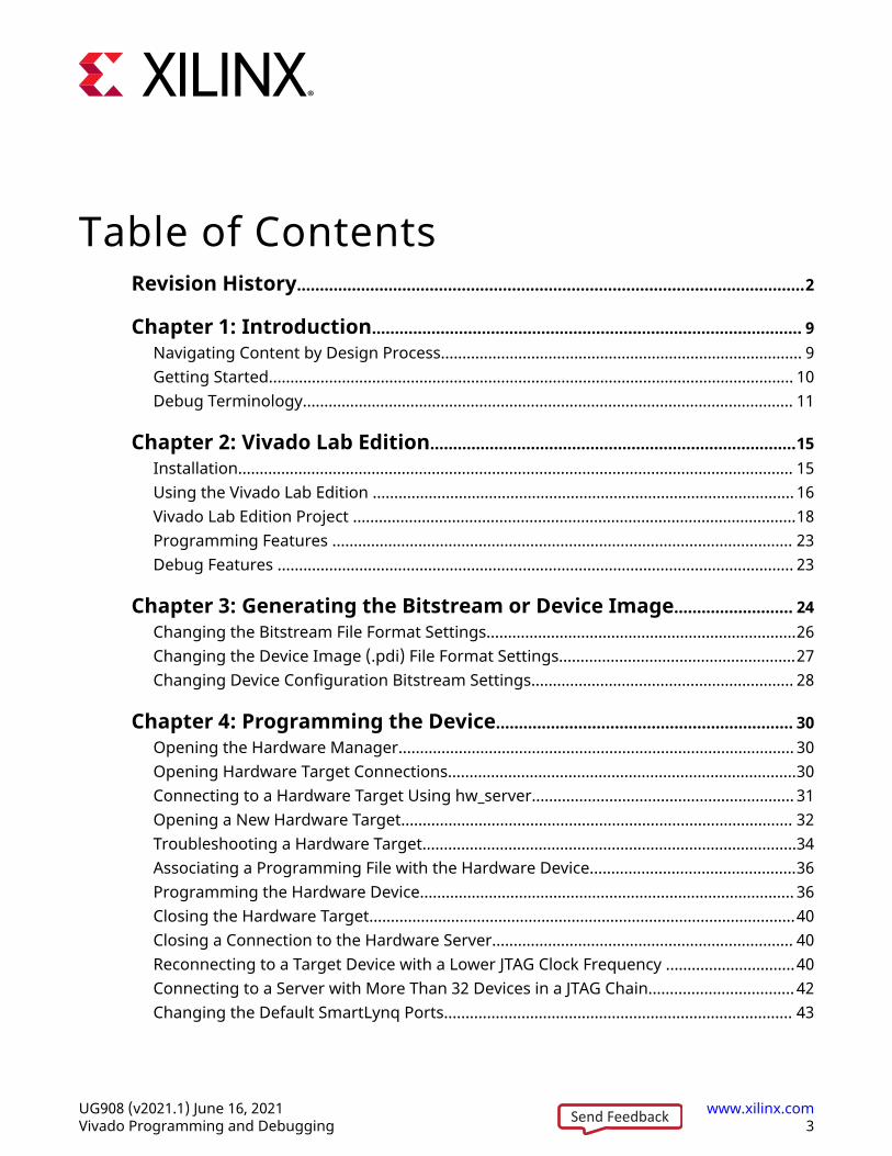
Table of ContentsRevision History...............................................................................................................2
Chapter 1: Introduction.............................................................................................. 9Navigating Content by Design Process.................................................................................... 9Getting Started.......................................................................................................................... 10Debug Terminology.................................................................................................................. 11
Chapter 2: Vivado Lab Edition................................................................................15Installation................................................................................................................................. 15Using the Vivado Lab Edition .................................................................................................. 16Vivado Lab Edition Project .......................................................................................................18Programming Features ........................................................................................................... 23Debug Features ........................................................................................................................ 23
Chapter 3: Generating the Bitstream or Device Image.......................... 24Changing the Bitstream File Format Settings........................................................................26Changing the Device Image (.pdi) File Format Settings.......................................................27Changing Device Configuration Bitstream Settings............................................................. 28
Chapter 4: Programming the Device................................................................. 30Opening the Hardware Manager............................................................................................ 30Opening Hardware Target Connections.................................................................................30Connecting to a Hardware Target Using hw_server............................................................. 31Opening a New Hardware Target........................................................................................... 32Troubleshooting a Hardware Target.......................................................................................34Associating a Programming File with the Hardware Device................................................36Programming the Hardware Device....................................................................................... 36Closing the Hardware Target...................................................................................................40Closing a Connection to the Hardware Server...................................................................... 40Reconnecting to a Target Device with a Lower JTAG Clock Frequency ..............................40Connecting to a Server with More Than 32 Devices in a JTAG Chain.................................. 42Changing the Default SmartLynq Ports................................................................................. 43
UG908 (v2021.1) June 16, 2021 www.xilinx.comVivado Programming and Debugging 3Send Feedback
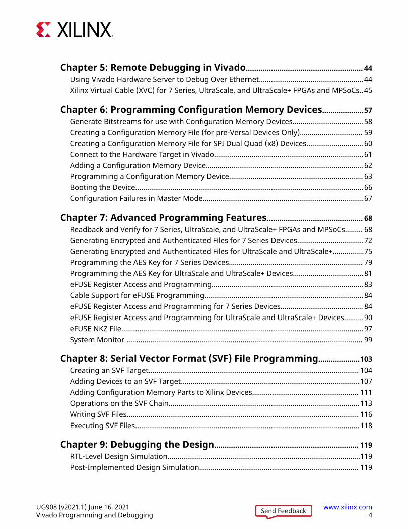
Chapter 5: Remote Debugging in Vivado........................................................ 44Using Vivado Hardware Server to Debug Over Ethernet..................................................... 44Xilinx Virtual Cable (XVC) for 7 Series, UltraScale, and UltraScale+ FPGAs and MPSoCs..45
Chapter 6: Programming Configuration Memory Devices....................57Generate Bitstreams for use with Configuration Memory Devices.................................... 58Creating a Configuration Memory File (for pre-Versal Devices Only)................................ 59Creating a Configuration Memory File for SPI Dual Quad (x8) Devices............................. 60Connect to the Hardware Target in Vivado............................................................................61Adding a Configuration Memory Device................................................................................ 62Programming a Configuration Memory Device.................................................................... 63Booting the Device.................................................................................................................... 66Configuration Failures in Master Mode..................................................................................67
Chapter 7: Advanced Programming Features.............................................. 68Readback and Verify for 7 Series, UltraScale, and UltraScale+ FPGAs and MPSoCs......... 68Generating Encrypted and Authenticated Files for 7 Series Devices..................................72Generating Encrypted and Authenticated Files for UltraScale and UltraScale+................75Programming the AES Key for 7 Series Devices.................................................................... 79Programming the AES Key for UltraScale and UltraScale+ Devices....................................81eFUSE Register Access and Programming............................................................................. 83Cable Support for eFUSE Programming.................................................................................84eFUSE Register Access and Programming for 7 Series Devices.......................................... 84eFUSE Register Access and Programming for UltraScale and UltraScale+ Devices..........90eFUSE NKZ File........................................................................................................................... 97System Monitor ........................................................................................................................ 99
Chapter 8: Serial Vector Format (SVF) File Programming....................103Creating an SVF Target........................................................................................................... 104Adding Devices to an SVF Target...........................................................................................107Adding Configuration Memory Parts to Xilinx Devices...................................................... 111Operations on the SVF Chain................................................................................................. 113Writing SVF Files...................................................................................................................... 116Executing SVF Files.................................................................................................................. 118
Chapter 9: Debugging the Design..................................................................... 119RTL-Level Design Simulation..................................................................................................119Post-Implemented Design Simulation................................................................................. 119
UG908 (v2021.1) June 16, 2021 www.xilinx.comVivado Programming and Debugging 4Send Feedback
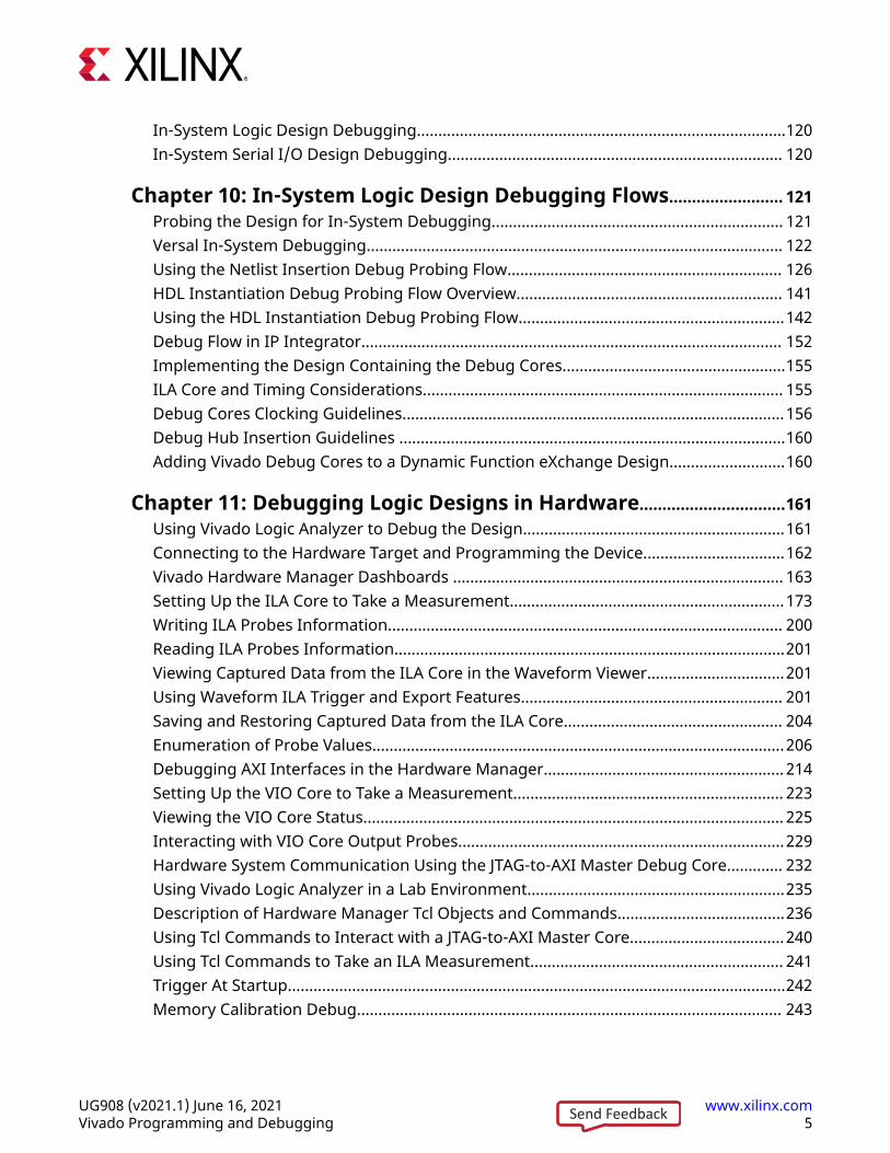
In-System Logic Design Debugging......................................................................................120In-System Serial I/O Design Debugging.............................................................................. 120
Chapter 10: In-System Logic Design Debugging Flows......................... 121Probing the Design for In-System Debugging.................................................................... 121Versal In-System Debugging................................................................................................. 122Using the Netlist Insertion Debug Probing Flow................................................................ 126HDL Instantiation Debug Probing Flow Overview.............................................................. 141Using the HDL Instantiation Debug Probing Flow..............................................................142Debug Flow in IP Integrator.................................................................................................. 152Implementing the Design Containing the Debug Cores....................................................155ILA Core and Timing Considerations.................................................................................... 155Debug Cores Clocking Guidelines.........................................................................................156Debug Hub Insertion Guidelines ..........................................................................................160Adding Vivado Debug Cores to a Dynamic Function eXchange Design...........................160
Chapter 11: Debugging Logic Designs in Hardware................................161Using Vivado Logic Analyzer to Debug the Design.............................................................161Connecting to the Hardware Target and Programming the Device.................................162Vivado Hardware Manager Dashboards ............................................................................. 163Setting Up the ILA Core to Take a Measurement................................................................173Writing ILA Probes Information............................................................................................ 200Reading ILA Probes Information...........................................................................................201Viewing Captured Data from the ILA Core in the Waveform Viewer................................201Using Waveform ILA Trigger and Export Features............................................................. 201Saving and Restoring Captured Data from the ILA Core................................................... 204Enumeration of Probe Values................................................................................................206Debugging AXI Interfaces in the Hardware Manager........................................................ 214Setting Up the VIO Core to Take a Measurement............................................................... 223Viewing the VIO Core Status.................................................................................................. 225Interacting with VIO Core Output Probes............................................................................229Hardware System Communication Using the JTAG-to-AXI Master Debug Core............. 232Using Vivado Logic Analyzer in a Lab Environment............................................................235Description of Hardware Manager Tcl Objects and Commands.......................................236Using Tcl Commands to Interact with a JTAG-to-AXI Master Core....................................240Using Tcl Commands to Take an ILA Measurement........................................................... 241Trigger At Startup....................................................................................................................242Memory Calibration Debug................................................................................................... 243
UG908 (v2021.1) June 16, 2021 www.xilinx.comVivado Programming and Debugging 5Send Feedback
Debugging Dynamic Function eXchange (DFX) Designs in Vivado HardwareManager.............................................................................................................................. 246
High Bandwidth Memory (HBM) Monitor............................................................................246PCI Express Link Debug..........................................................................................................248
Chapter 12: Viewing ILA Probe Data in the Waveform Viewer......... 251ILA Data and Waveform Relationship...................................................................................251Waveform Viewer Layout ...................................................................................................... 252Waveform Viewer Operation ................................................................................................ 253Removing Probes from the Waveform.................................................................................254Adding Probes to the Waveform...........................................................................................255Using Waveform ILA Trigger and Export Features ............................................................ 256Using the Zoom Features ...................................................................................................... 257Waveform Settings..................................................................................................................258Customizing the Configuration............................................................................................. 259Renaming Objects...................................................................................................................263Bus Radixes.............................................................................................................................. 265Viewing Analog Waveforms................................................................................................... 266Bus Plot Viewer........................................................................................................................268Zoom Gestures........................................................................................................................ 271
Chapter 13: Debugging Designs Post Implementation.........................272Using Vivado ECO Flow to Replace Existing Debug Probes............................................... 272Replacing Debug Probes on a Placed and Routed Design Checkpoint............................273Vivado ECO TCL Flow to Replace Existing Debug Probes...................................................279Incremental Compile with Debug Core (ILA) Modifications.............................................. 279
Chapter 14: Serial I/O Hardware Debugging Flows.................................283Serial I/O Hardware Debugging Flows.................................................................................283
Chapter 15: Versal Serial I/O Hardware Debugging Flows..................289
Chapter 16: Debugging the Serial I/O Design in Hardware................290Using Vivado Serial I/O Analyzer to Debug the Design......................................................290Viewing Slicer Eye, Histogram, and Signal-to-Noise Ratio (GTM Transceivers Only)..... 305
Appendix A: Device Configuration Bitstream or PDI Settings.......... 3077 Series Bitstream Settings.................................................................................................... 307Zynq-7000 Bitstream Settings................................................................................................312
UG908 (v2021.1) June 16, 2021 www.xilinx.comVivado Programming and Debugging 6Send Feedback
UltraScale Bitstream Settings................................................................................................ 317Virtex and Kintex UltraScale+ Bitstream Settings............................................................... 323Zynq UltraScale+ MPSoC Bitstream Settings....................................................................... 329Versal ACAP Programmable Device Image (PDI) Settings.................................................331
Appendix B: Trigger State Machine Language Description................333States........................................................................................................................................ 333Goto Action.............................................................................................................................. 333Conditional Branching............................................................................................................334Counters................................................................................................................................... 334Flags..........................................................................................................................................335Conditional Statements..........................................................................................................335
Appendix C: Low Level SVF JTAG Commands...............................................341Header Data Register (HDR), Header Instruction Register (HIR)......................................341TDR, TIR (Trailer Data Register, Trailer Instruction Register) ........................................... 342scan_ir_hw................................................................................................................................ 343scan_dr_hw...............................................................................................................................344Multi Chain SVF Operation..................................................................................................... 345
Appendix D: JTAG Cables and Devices Supported by hw_server...... 349
Appendix E: Configuration Memory Support..............................................350Artix-7 Configuration Memory Devices................................................................................ 350Kintex-7 Configuration Memory Devices..............................................................................354Spartan-7 Configuration Memory Devices...........................................................................358Virtex-7 Configuration Memory Devices.............................................................................. 360Kintex UltraScale Configuration Memory Devices.............................................................. 363Kintex UltraScale+ Configuration Memory Devices............................................................ 368Virtex UltraScale Configuration Memory Devices............................................................... 371Virtex UltraScale+ Configuration Memory Devices............................................................. 375Zynq-7000 Configuration Memory Devices..........................................................................378Zynq UltraScale+ MPSoC Configuration Memory Devices................................................. 396Zynq UltraScale+ RFSoC Configuration Memory Devices...................................................403Versal Configuration Memory Devices................................................................................. 411
Appendix F: Command Line Options for hw_server................................ 420Standard hw_server Options................................................................................................. 420Advanced Options................................................................................................................... 422
UG908 (v2021.1) June 16, 2021 www.xilinx.comVivado Programming and Debugging 7Send Feedback
Appendix G: Additional Resources and Legal Notices........................... 428Xilinx Resources.......................................................................................................................428Solution Centers...................................................................................................................... 428Documentation Navigator and Design Hubs...................................................................... 428References................................................................................................................................429Training Courses..................................................................................................................... 430Please Read: Important Legal Notices................................................................................. 431
UG908 (v2021.1) June 16, 2021 www.xilinx.comVivado Programming and Debugging 8Send Feedback
Chapter 1
Introduction
Navigating Content by Design ProcessXilinx® documentation is organized around a set of standard design processes to help you findrelevant content for your current development task. All Versal™ ACAP design process DesignHubs can be found on the Xilinx.com website. This document covers the following designprocesses:
• Hardware, IP, and Platform Development: Creating the PL IP blocks for the hardwareplatform, creating PL kernels, functional simulation, and evaluating the Vivado® timing,resource use, and power closure. Also involves developing the hardware platform for systemintegration. Topics in this document that apply to this design process include:
• Chapter 9: Debugging the Design
• Chapter 10: In-System Logic Design Debugging Flows
• Chapter 11: Debugging Logic Designs in Hardware
• Chapter 12: Viewing ILA Probe Data in the Waveform Viewer
• Chapter 13: Debugging Designs Post Implementation
• Board System Design: Designing a PCB through schematics and board layout. Also involvespower, thermal, and signal integrity considerations. Topics in this document that apply to thisdesign process include:
• Chapter 4: Programming the Device
• Chapter 5: Remote Debugging in Vivado
• Chapter 6: Programming Configuration Memory Devices
• Chapter 7: Advanced Programming Features
• Chapter 8: Serial Vector Format (SVF) File Programming
• Chapter 14: Serial I/O Hardware Debugging Flows
• Chapter 16: Debugging the Serial I/O Design in Hardware
• Appendix A: Device Configuration Bitstream or PDI Settings
• Appendix C: Low Level SVF JTAG Commands
Chapter 1: Introduction
UG908 (v2021.1) June 16, 2021 www.xilinx.comVivado Programming and Debugging 9Send Feedback
• Appendix D: JTAG Cables and Devices Supported by hw_server
• Appendix E: Configuration Memory Support
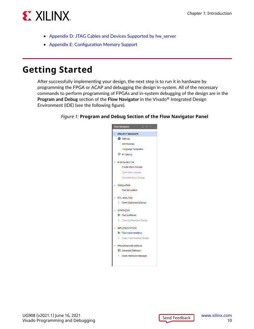
Getting StartedAfter successfully implementing your design, the next step is to run it in hardware byprogramming the FPGA or ACAP and debugging the design in-system. All of the necessarycommands to perform programming of FPGAs and in-system debugging of the design are in theProgram and Debug section of the Flow Navigator in the Vivado® Integrated DesignEnvironment (IDE) (see the following figure).
Figure 1: Program and Debug Section of the Flow Navigator Panel
Chapter 1: Introduction
UG908 (v2021.1) June 16, 2021 www.xilinx.comVivado Programming and Debugging 10Send Feedback
Debug TerminologyILAThe Integrated Logic Analyzer (ILA) feature allows you to perform in-system debugging of post-implemented designs on an FPGA, SoC, or Versal™ device. This feature should be used whenthere is a need to monitor signals in the design. You can also use this feature to trigger onhardware events and capture data at system speeds.
The ILA core can be instantiated in your RTL code or inserted post synthesis in the Vivado designflow. Detailed documentation on the ILA core IP can be found in the Integrated Logic AnalyzerLogiCORE IP Product Guide (PG172).
Related Information
In-System Logic Design Debugging FlowsDebugging Logic Designs in Hardware
VIOThe Virtual Input/Output (VIO) debug feature can both monitor and drive internal FPGA, SoC, orVersal ACAP signals in real time. In the absence of physical access to the target hardware, youcan use this debug feature to drive and monitor signals that are present on the real hardware.
This debug core needs to be instantiated in the RTL code, hence you need to know up-front,what nets to drive. The IP Catalog lists this core under the Debug category. Detaileddocumentation on the VIO core IP can be found in the Virtual Input/Output LogiCORE IP ProductGuide (PG159).
Related Information
Debugging Logic Designs in Hardware
IBERTThe Integrated Bit Error Ratio Tester (IBERT) Serial Analyzer design enables in-system serial I/Ovalidation and debug. This allows you to measure and optimize your high-speed serial I/O links inyour FPGA-based system. Xilinx recommends using the IBERT Serial Analyzer design when youare interested in addressing a range of in-system debug and validation problems from simpleclocking and connectivity issues to complex margin analysis and channel optimization issues.
Chapter 1: Introduction
UG908 (v2021.1) June 16, 2021 www.xilinx.comVivado Programming and Debugging 11Send Feedback
Xilinx recommends using the IBERT Serial Analyzer design when you are interested in measuringthe quality of a signal after a receiver equalization has been applied to the received signal. Thisensures that you are measuring at the optimal point in the TX-to-RX channel thereby ensuringreal and accurate data. Users can access this design by selecting, configuring, and generating theIBERT core from the IP Catalog and selecting the Open Example Design feature of this core. See Serial I/O Hardware Debugging Flows and Chapter 16: Debugging the Serial I/O Design inHardware for more details on the IBERT core and its usage methodology in the Vivado DesignSuite.
Related Information
Debugging the Serial I/O Design in HardwareSerial I/O Hardware Debugging Flows
JTAG-to-AXI MasterNote: The JTAG-to-AXI Master is not supported on Versal ACAP devices as the built-in CIPS AXI Masterinterfaces can be used in combination with the Debug Packet Controller (DPC) to generate AXItransactions without additional IP.
The JTAG-to-AXI Master debug feature is used to generate AXI transactions that interact withvarious AXI full and AXI lite slave cores in a system that is running in hardware. Xilinxrecommends that you use this core to generate AXI transactions and debug/drive AXI signalsinternal to an FPGA at run time. This core can be used in designs without processors as well.
The IP Catalog lists this core under the Debug category. Debugging Logic Designs in Hardware ofthis guide has more details about the JTAG-to-AXI Master core and its usage methodology in theVivado Design Suite. Detailed documentation on the JTAG-to-AXI IP core can be found in theJTAG to AXI Master LogiCORE IP Product Guide (PG174).
Related Information
Debugging Logic Designs in Hardware
Debug HubOn 7 series and UltraScale architectures the Vivado Debug Hub core provides an interfacebetween the JTAG Boundary Scan (BSCAN) interface of the FPGA device and the Vivado Debugcores including the following types of cores:
• Integrated Logic Analyzer (ILA)
• Virtual Input/Output (VIO)
• Integrated Bit Error Ratio Test (IBERT)
• JTAG-to-AXI
Chapter 1: Introduction
UG908 (v2021.1) June 16, 2021 www.xilinx.comVivado Programming and Debugging 12Send Feedback
• Memory IP
IMPORTANT! The Vivado Debug Hub core cannot be instantiated into the design. It is inserted byVivado during the opt_design stage.
AXI4 Debug HubOn Versal™ ACAP architectures the AXI4 Debug Hub is an IP core that provides an interfacebetween the AXI4 Master interface of the CIPS and the AXI4-Stream interface on the VivadoHardware Debug cores including the following:
• Integrated Logic Analyzer (ILA)
• Virtual Input/Output (VIO)
• Soft Memory IP
Note: On Versal devices, the AXI4 Debug Hub can be manually instantiated as an IP or insertedautomatically during opt_design, just as with previous architectures.
System ILAThe System Integrated Logic Analyzer (System ILA) IP core is a logic analyzer that allows you toperform in-system debugging of post-implemented designs on an FPGA device. Use this IP whenyou need to monitor interfaces and signals in the IP integrator Block Design. You can also usethis feature to trigger on interface and signal related hardware events and capture data at systemspeeds. This ensures the intuitive presentation of interface events in the Hardware Managerwhen debugging the design on an FPGA or ACAP. This IP offers AXI interface debug andmonitoring capability along with AXI4-MM and AXI4-Stream protocol checking.
Since the System ILA core is synchronous to the design being monitored, all design clockconstraints that are applied to your design are also applied to the components of the System ILAcore. Detailed documentation on the System ILA core IP can be found in the System IntegratedLogic Analyzer LogiCORE IP Product Guide (PG261).
Note: On Versal™ devices the System ILA functionality is available using the Versal ILA core.
Debug BridgeNote: The Debug Bridge IP is not supported on Versal architectures.
The Debug Bridge IP core is a controller that provides multiple options to communicate with thedebug cores in the design.
The primary use case for a Debug Bridge is to use a Xilinx Virtual Cable (XVC) to remotely debugdesigns through Ethernet or other interfaces without the need for a JTAG cable.
Chapter 1: Introduction
UG908 (v2021.1) June 16, 2021 www.xilinx.comVivado Programming and Debugging 13Send Feedback
The other common use case is for debugging Dynamic Function eXchange and Tandem PCIe withField Updates designs. For more information on the Tandem PCIe with Field Updates flow andDebug Bridge refer to UltraScale+ Devices Integrated Block for PCI Express LogiCORE IP ProductGuide (PG213).
The Debug Bridge can also be used with the PCIe® core in systems where JTAG is not thepreferred communication and debug mechanism. For more information on the using the XVCflow with the PCIe core and Debug Bridge refer to UltraScale+ Devices Integrated Block for PCIExpress LogiCORE IP Product Guide (PG213).
Detailed documentation on the Debug Bridge core IP can be found in the Debug Bridge LogiCOREIP Product Guide (PG245).
In-System IBERTNote: In-System IBERT is supported on UltraScale and UltraScale+ only.
The In-System IBERT IP enables you to perform 2-D eye-scans of UltraScale and UltraScale+transceivers in your design, using the Vivado Serial IO Analyzer. The IP uses data from the designto plot the eye-scan of the transceivers in real time while they interact with the rest of thesystem. This IP can be integrated with user logic in the design or Xilinx transceiver based IPs (forexample GT Wizard, or Aurora, etc.).
Detailed documentation on the In-System IBERT IP can be found in the In-System IBERTLogiCORE IP Product Guide (PG246).
IBERT GTRIBERT UltraScale+ GTR can be used to evaluate and monitor GTR transceivers in Zynq UltraScale+ MPSoC devices. With this feature, you can accomplish the following tasks:
• Perform eye scans with user data
• Change GTR settings
• View link status
• Check the "lock" status of all PLLs used by all GTR lanes
However, IBERT GTR does not provide the following capabilities:
• Perform eye scans with raw PRBS data patterns
• Measure Bit Error Ratio (no bit or error counters)
Note that this solution is software based, meaning that no IP or logic is required in theprogrammable logic of the device.
Chapter 1: Introduction
UG908 (v2021.1) June 16, 2021 www.xilinx.comVivado Programming and Debugging 14Send Feedback

Chapter 2
Vivado Lab EditionVivado® Lab Edition is a standalone installation of the full Vivado Design Suite with all thefeatures and capabilities required to program and debug Xilinx® devices after generating thedevice image. Typical usage is for programming and debug in the lab environment wheremachines have a smaller amount of resources in terms of disk space, memory, and connectivity.Vivado Lab Edition has a reduced product footprint of around 2.4 GB after installation and theinstall package size is 1 GB.
InstallationTo install the Vivado Lab Edition, select Lab Edition from the Unified Installer.
Detailed installation, licensing and release information is available in Vivado Design Suite UserGuide: Release Notes, Installation, and Licensing (UG973).
Launching Vivado Lab Edition on WindowsTo launch Vivado Lab Edition, select the following:
Start → All Programs → Xilinx Design Tools → Vivado Lab 2020.2 → Vivado Lab 2021.1
Launching the Vivado Lab Edition from theCommand Line on Windows or LinuxEnter the following command at the command prompt:
vivado_lab
TIP: To run vivado_lab at the command prompt, set up your environment using the following script:
C:\Xilinx\Vivado_Lab\2020.x\settings64.(bat|sh)
Chapter 2: Vivado Lab Edition
UG908 (v2021.1) June 16, 2021 www.xilinx.comVivado Programming and Debugging 15Send Feedback
You can open the Vivado Lab Edition from any directory. However, Xilinx recommends running itfrom a writable project directory, because the Vivado Lab Edition log and journal files are writtento the launch directory. When running from a command prompt, launch the Vivado IDE from theproject directory, or use the vivado_lab -log and journal options to specify a location.When using a Windows shortcut, you must modify the Start in folder, which is a property of theshortcut. Failure to launch from a writable project directory results in warnings and unpredictablebehavior from the tool.
Using the Vivado Lab EditionWhen you launch the Vivado Lab Edition, the Getting Started page (see the following figure)displays and provides you with different options to help you begin working with the Vivado LabEdition.
Chapter 2: Vivado Lab Edition
UG908 (v2021.1) June 16, 2021 www.xilinx.comVivado Programming and Debugging 16Send Feedback

Figure 2: Vivado Lab Edition Welcome Screen
Starting with a ProjectTo program or debug your design, you can create or open a project, and connect to a targetserver and device. The Quick Start section of the Getting Started Page provides links for easyaccess to the following tasks:
• Create a project.
• Open existing projects
Note: You can also open recently accessed projects from the Recent Projects list.
Chapter 2: Vivado Lab Edition
UG908 (v2021.1) June 16, 2021 www.xilinx.comVivado Programming and Debugging 17Send Feedback
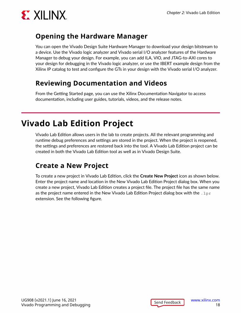
Opening the Hardware ManagerYou can open the Vivado Design Suite Hardware Manager to download your design bitstream toa device. Use the Vivado logic analyzer and Vivado serial I/O analyzer features of the HardwareManager to debug your design. For example, you can add ILA, VIO, and JTAG-to-AXI cores toyour design for debugging in the Vivado logic analyzer, or use the IBERT example design from theXilinx IP catalog to test and configure the GTs in your design with the Vivado serial I/O analyzer.
Reviewing Documentation and VideosFrom the Getting Started page, you can use the Xilinx Documentation Navigator to accessdocumentation, including user guides, tutorials, videos, and the release notes.
Vivado Lab Edition ProjectVivado Lab Edition allows users in the lab to create projects. All the relevant programming andruntime debug preferences and settings are stored in the project. When the project is reopened,the settings and preferences are restored back into the tool. A Vivado Lab Edition project can becreated in both the Vivado Lab Edition tool as well as in Vivado Design Suite.
Create a New ProjectTo create a new project in Vivado Lab Edition, click the Create New Project icon as shown below.Enter the project name and location in the New Vivado Lab Edition Project dialog box. When youcreate a new project, Vivado Lab Edition creates a project file. The project file has the same nameas the project name entered in the New Vivado Lab Edition Project dialog box with the .lprextension. See the following figure.
Chapter 2: Vivado Lab Edition
UG908 (v2021.1) June 16, 2021 www.xilinx.comVivado Programming and Debugging 18Send Feedback
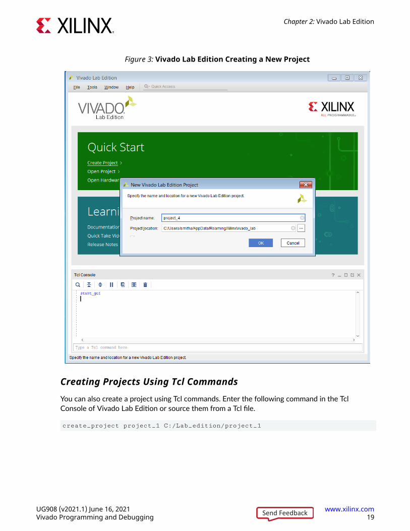
Figure 3: Vivado Lab Edition Creating a New Project
Creating Projects Using Tcl Commands
You can also create a project using Tcl commands. Enter the following command in the TclConsole of Vivado Lab Edition or source them from a Tcl file.
create_project project_1 C:/Lab_edition/project_1
Chapter 2: Vivado Lab Edition
UG908 (v2021.1) June 16, 2021 www.xilinx.comVivado Programming and Debugging 19Send Feedback

Opening the ProjectTo open existing projects, click the open project icon as shown in the following figure or double-click a project in the Recent Projects list. This opens a browser that enables you to open anyVivado Lab Edition project file (.lpr extension). By default, the last ten previously openedprojects are listed in the Recent Projects list. To change this number, click Tools → Settings andupdate the Project options. Vivado Lab Edition checks to ensure that the project data is availablebefore displaying the projects.
Chapter 2: Vivado Lab Edition
UG908 (v2021.1) June 16, 2021 www.xilinx.comVivado Programming and Debugging 20Send Feedback
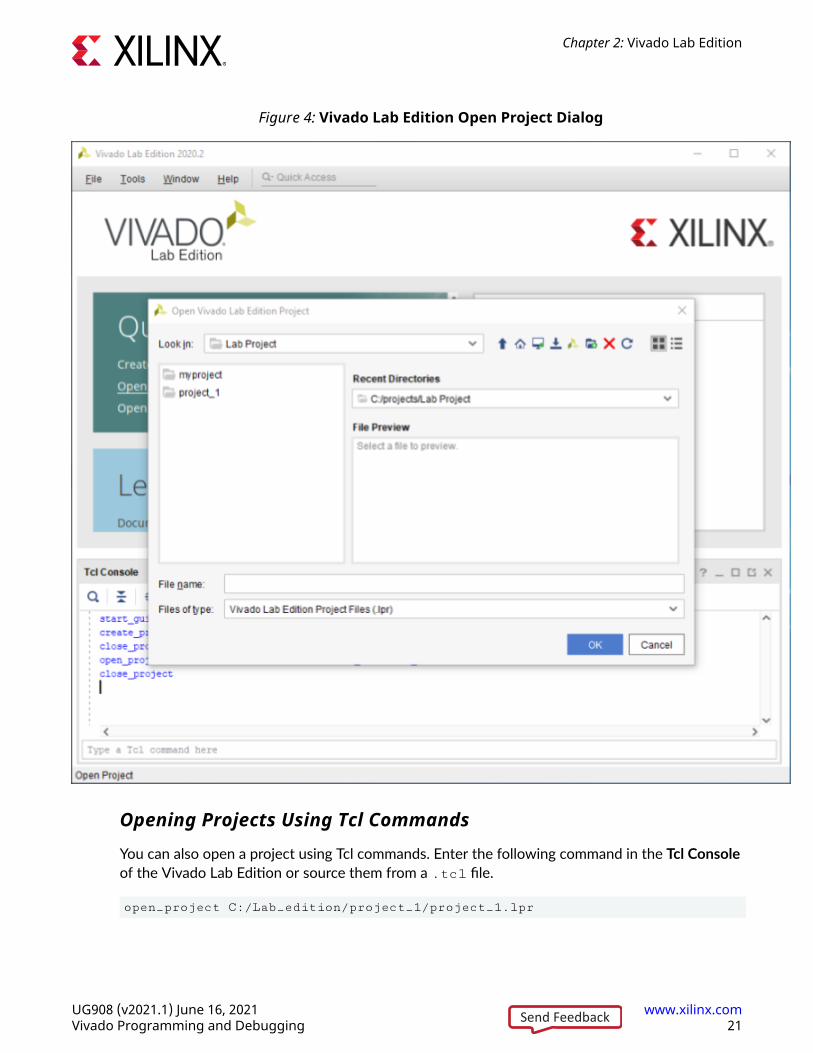
Figure 4: Vivado Lab Edition Open Project Dialog
Opening Projects Using Tcl Commands
You can also open a project using Tcl commands. Enter the following command in the Tcl Consoleof the Vivado Lab Edition or source them from a .tcl file.
open_project C:/Lab_edition/project_1/project_1.lpr
Chapter 2: Vivado Lab Edition
UG908 (v2021.1) June 16, 2021 www.xilinx.comVivado Programming and Debugging 21Send Feedback

Using an Existing Device Image and Debug ProbesFiles in Vivado Lab EditionYou can use the existing device image (.bit or .pdi) and .ltx file from a previousimplementation run in the lab machine where Vivado Lab Edition is installed.
Typical flow would entail the following:
1. Create a new Vivado Lab Edition project.
2. Connect to the board.
3. Specify the .bit or .pdi file and .ltx file for the project.
4. You can either manually copy these files or point to them on a network drive.
5. Program the device.
6. Debug the design in your hardware.
7. Changes are continuously saved to the project
8. User preferences, runtime manager debug dashboard, and window settings are continuouslysaved to the project.
9. User preferences, runtime manager debug dashboard, and window settings are restored atproject reopen.
Using an Existing .lpr Project from Vivado DesignSuite EditionVivado Design Suite creates an .lpr file at project startup and populates this file withappropriate details when you use the Hardware Manager to program and/or debug the design inthe project. This file is located in the project_name.hw directory and is namedproject_name.lpr. This project file can be opened in the Vivado Lab Edition.
Typical flow would entail:
1. Click the Open Project icon on the Vivado Lab Edition start page.
2. Traverse to the project_name.hw directory, which is located inside the Vivado IDE projectdirectory
3. Select the .lpr project file inside the project_name.hw directory and click OK.
4. Connect to your hardware.
5. Program and debug with the correct device image file and .ltx file from the appropriateVivado runs directory
6. User preferences, runtime manager debug dashboard, and window settings are restored atproject open.
Chapter 2: Vivado Lab Edition
UG908 (v2021.1) June 16, 2021 www.xilinx.comVivado Programming and Debugging 22Send Feedback
Programming FeaturesAfter the project is open and the Hardware Manager is connected with a target device, you canuse all the programming features that were available in the Vivado Design Suite from the VivadoLab Edition. All the programming related Tcl commands are supported in Vivado Lab Edition. Formore details on the programming features available refer to Programming Configuration MemoryDevices.
Related Information
Programming Configuration Memory Devices
Debug FeaturesAfter you open the project and connect the Hardware Manager with a target device, you can useall the debug features that were available in the Vivado Design Suite from the Vivado LabEdition. All the debug related Tcl commands are supported in Vivado Lab Edition. For moredetails on the debug features available refer to Debugging Logic Designs in Hardware of this userguide.
Related Information
Debugging Logic Designs in Hardware
Chapter 2: Vivado Lab Edition
UG908 (v2021.1) June 16, 2021 www.xilinx.comVivado Programming and Debugging 23Send Feedback
Chapter 3
Generating the Bitstream or DeviceImage
Before generating a bitstream or device image, it is important to review the settings to make surethey are correct for your design.
There are two types of bitstream and device image settings in Vivado® IDE:
1. Bitstream or Device Image file format settings.
2. Device configuration settings.
Select Settings → Bitstream in the Vivado Flow Navigator or Flow → Settings → BitstreamSettings... menu selection to open the Bitstream Settings popup window (see the followingfigure). Once the settings are correct, the bitstream data file can be generated using thewrite_bistream Tcl command or by using the Generate Bitstream button in the Vivado flownavigator.
If a Versal™ device is targeted, a programmable device image (.pdi) is generated instead of abitstream. The procedure to change the device image settings is similar to previous architectureshowever the menu options, Tcl commands, and available settings will differ. To access the deviceimage settings select Settings → Generate Device Image in the Vivado Flow Navigator or Flow → Settings → Generate Device Image Settings... menu selection to open the Device Image sectionin the Settings popup window (see the following figure). The device image data file can begenerated using the write_device_image Tcl command or by using the Write Device Imagebutton in the Vivado flow navigator. For more details about the PDI format, refer to the BootgenUser Guide (UG1283).
Chapter 3: Generating the Bitstream or Device Image
UG908 (v2021.1) June 16, 2021 www.xilinx.comVivado Programming and Debugging 24Send Feedback
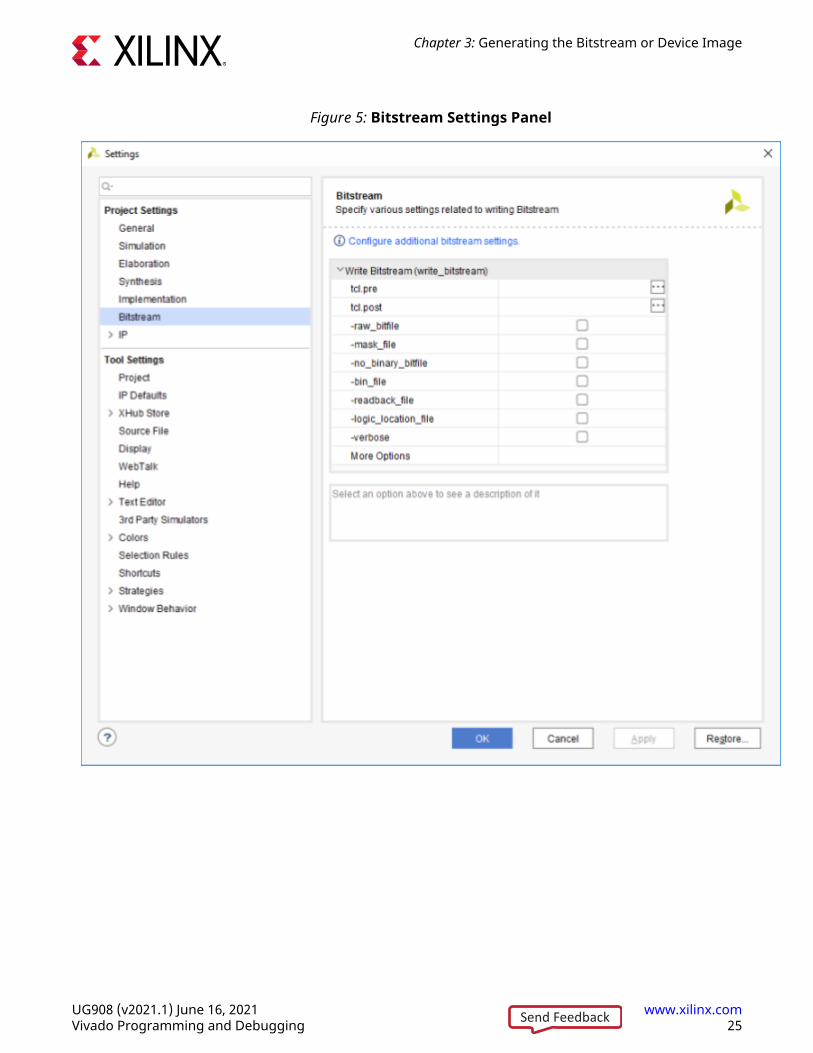
Figure 5: Bitstream Settings Panel
Chapter 3: Generating the Bitstream or Device Image
UG908 (v2021.1) June 16, 2021 www.xilinx.comVivado Programming and Debugging 25Send Feedback
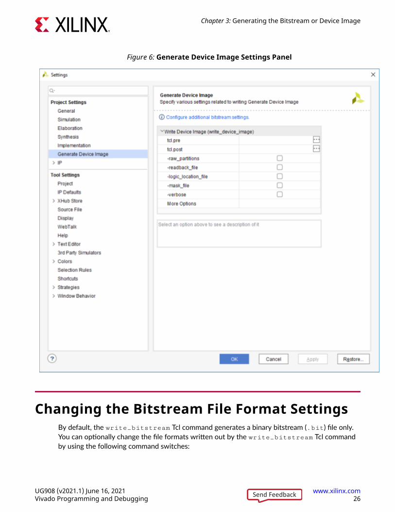
Figure 6: Generate Device Image Settings Panel
Changing the Bitstream File Format SettingsBy default, the write_bitstream Tcl command generates a binary bitstream (.bit) file only.You can optionally change the file formats written out by the write_bitstream Tcl commandby using the following command switches:
Chapter 3: Generating the Bitstream or Device Image
UG908 (v2021.1) June 16, 2021 www.xilinx.comVivado Programming and Debugging 26Send Feedback
• -raw_bitfile: (Optional) This switch causes write_bitstream to write a raw bit file (.rbt), whichcontains the same information as the binary bitstream file, but is in ASCII format. The outputfile is named filename .rbt.
• -mask_file: (Optional) Write a mask file (.msk), which has mask data where the configurationdata is in the bitstream file. This file determines which bits in the bitstream should becompared to readback data for verification purposes. If a mask bit is 0, that bit should beverified against the bitstream data. If a mask bit is 1, that bit should not be verified. Theoutput file is named file.msk.
• -no_binary_bitfile: (Optional) Do not write the binary bitstream file (.bit). Use this commandwhen you want to generate the ASCII bitstream or mask file, or to generate a bitstream report,without generating the binary bitstream file.
• -logic_location_file: (Optional) Creates an ASCII logic location file (.ll) that shows thebitstream position of latches, flip-flops, LUTs, Block RAMs, and I/O block inputs and outputs.Bits are referenced by frame and bit number in the location file to help you observe thecontents of FPGA registers.
• -bin_file: (Optional) Creates a binary file (.bin) containing only device programming data,without the header information found in the standard bitstream file (.bit).
• -reference_bitfile <arg>: (Optional) Read a reference bitstream file, and output an incrementalbitstream file containing only the differences from the specified reference file. This partialbitstream file can be used for incrementally programming an existing device with an updateddesign.
Changing the Device Image (.pdi) File FormatSettings
By default, the write_device_image Tcl command generates a (.pdi) file only. You canoptionally change the file formats written out by the write_device_image Tcl command byusing the following command switches:
• -force (Optional): Overwrite existing file.
• -verbose (Optional): Print write_device_image options.
• -raw_partitions (Optional): Write raw CFI and NPI partition files (.rnpi and .rcdo)
• -mask_file (Optional): Write a mask file (.msk)
• -logic_location_file (Optional): Write logic location file (.ll)
• -cell <arg> (Optional): Create only partial device image for the named cell.
• -no_pdi Do not generate a pdi file. Stop after generating raw partitions files only.
• -no_partial_pdifile (Optional): Do not write partial pdi files for a Dynamic FunctioneXchange design.
Chapter 3: Generating the Bitstream or Device Image
UG908 (v2021.1) June 16, 2021 www.xilinx.comVivado Programming and Debugging 27Send Feedback
• -quiet (Optional): Ignore command errors.
• <file> (Required): The name of the .pdi file to write.
Changing Device Configuration BitstreamSettings
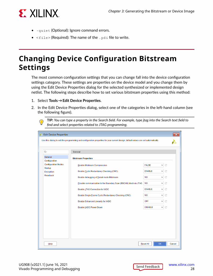
The most common configuration settings that you can change fall into the device configurationsettings category. These settings are properties on the device model and you change them byusing the Edit Device Properties dialog for the selected synthesized or implemented designnetlist. The following steps describe how to set various bitstream properties using this method:
1. Select Tools → Edit Device Properties.
2. In the Edit Device Properties dialog, select one of the categories in the left-hand column (seethe following figure).
TIP: You can type a property in the Search field. For example, type jtag into the Search text field tofind and select properties related to JTAG programming.
Chapter 3: Generating the Bitstream or Device Image
UG908 (v2021.1) June 16, 2021 www.xilinx.comVivado Programming and Debugging 28Send Feedback
3. Set the properties to the desired values, and click OK.
4. Select File → Constraints → Save to save the updated properties to the target XDC file.
You can also set the bitstream properties using the set_property command in an XDC file. Forinstance, here is an example on how to change the start-up DONE cycle property:
set_property BITSTREAM.STARTUP.DONE_CYCLE 4 [current_design]
Additional examples and templates are provided in the Vivado Templates. Device ConfigurationBitstream Settings describes all of the device configuration settings.
IMPORTANT! Edit only the Device Configuration Bitstream Settings relevant to the configuration modebeing used. Leave the other settings at their default values
Related Information
Device Configuration Bitstream or PDI Settings
Chapter 3: Generating the Bitstream or Device Image
UG908 (v2021.1) June 16, 2021 www.xilinx.comVivado Programming and Debugging 29Send Feedback
Chapter 4
Programming the DeviceThe next step after generating the device image is to download it into the target device. VivadoIDE has native in-system device programming capabilities built in to do this.
Vivado Design Suite and Vivado Lab Edition includes functionality that allows you to connect tohardware containing one or more FPGAs or ACAPs to program and interact with those devices.Connecting to hardware can be done from either the Vivado Lab Edition, or Vivado Design Suitegraphical user interface or by using Tcl commands. In either case, the steps to connect tohardware and program the target device are the same:
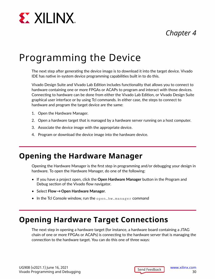
1. Open the Hardware Manager.
2. Open a hardware target that is managed by a hardware server running on a host computer.
3. Associate the device image with the appropriate device.
4. Program or download the device image into the hardware device.
Opening the Hardware ManagerOpening the Hardware Manager is the first step in programming and/or debugging your design inhardware. To open the Hardware Manager, do one of the following:
• If you have a project open, click the Open Hardware Manager button in the Program andDebug section of the Vivado flow navigator.
• Select Flow → Open Hardware Manager.
• In the Tcl Console window, run the open_hw_manager command
Opening Hardware Target ConnectionsThe next step in opening a hardware target (for instance, a hardware board containing a JTAGchain of one or more FPGAs or ACAPs) is connecting to the hardware server that is managing theconnection to the hardware target. You can do this one of three ways:
Chapter 4: Programming the Device
UG908 (v2021.1) June 16, 2021 www.xilinx.comVivado Programming and Debugging 30Send Feedback
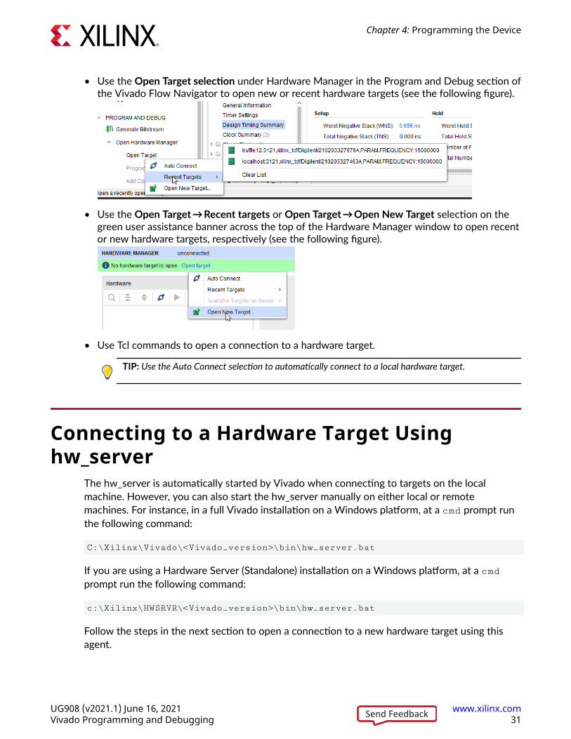
• Use the Open Target selection under Hardware Manager in the Program and Debug section ofthe Vivado Flow Navigator to open new or recent hardware targets (see the following figure).
• Use the Open Target → Recent targets or Open Target → Open New Target selection on thegreen user assistance banner across the top of the Hardware Manager window to open recentor new hardware targets, respectively (see the following figure).
• Use Tcl commands to open a connection to a hardware target.
TIP: Use the Auto Connect selection to automatically connect to a local hardware target.
Connecting to a Hardware Target Usinghw_server
The hw_server is automatically started by Vivado when connecting to targets on the localmachine. However, you can also start the hw_server manually on either local or remotemachines. For instance, in a full Vivado installation on a Windows platform, at a cmd prompt runthe following command:
C:\Xilinx\Vivado\<Vivado_version>\bin\hw_server.bat
If you are using a Hardware Server (Standalone) installation on a Windows platform, at a cmdprompt run the following command:
c:\Xilinx\HWSRVR\<Vivado_version>\bin\hw_server.bat
Follow the steps in the next section to open a connection to a new hardware target using thisagent.
Chapter 4: Programming the Device
UG908 (v2021.1) June 16, 2021 www.xilinx.comVivado Programming and Debugging 31Send Feedback
For a list of compatable JTAG download cables and devices see Appendix D: JTAG Cables andDevices Supported by hw_server.
For more information on using SmartLynq data cables, see the SmartLynq Data Cable User Guide(UG1258).
IMPORTANT! If Vivado Hardware Manager is connected to the hw_server, and the hw_server is stopped,the Hardware Manager detects this condition automatically and disconnects from the server.
Opening a New Hardware TargetThe Open New Hardware Target wizard provides an interactive way for you to connect to ahardware server and target. The wizard process has the following steps:
1. Select a local or remote server, depending on what machine your hardware target isconnected to:
• Local server: Use this setting if your hardware target is connected to the same machine onwhich you are running the Vivado Lab Edition or Vivado IDE (See the following figure). TheVivado software automatically starts the Vivado hardware server (hw_server) applicationon the local machine.
• Remote server: Use this setting if your hardware target is connected to a different machineon which you are running the Vivado Lab Edition or Vivado IDE. Specify the host name orIP address of the remote machine and the port number for the hardware server(hw_server) application that is running on that machine (see the following figures). Refer toConnecting to a Remote hw_server Running on a Lab Machine for more details on remotedebugging.
IMPORTANT! When using remote server, you need to manually start the Vivado hardware server(hw_server) application of the same version of Vivado software that you will use to connect to thehardware server.
TIP: If you only want to connect to your lab machine remotely, you do not need to install the fullVivado design suite on that remote machine. Instead, you can install the light-weight Vivado HardwareServer (Standalone) tool on the remote machine.
Chapter 4: Programming the Device
UG908 (v2021.1) June 16, 2021 www.xilinx.comVivado Programming and Debugging 32Send Feedback
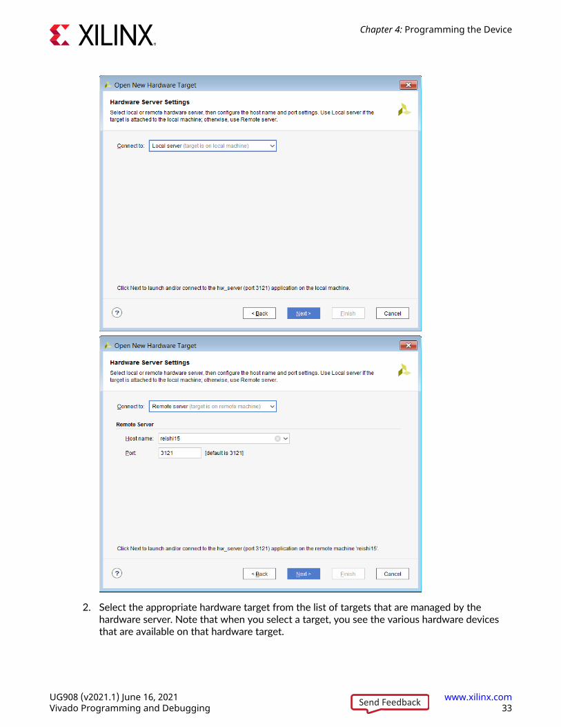
2. Select the appropriate hardware target from the list of targets that are managed by thehardware server. Note that when you select a target, you see the various hardware devicesthat are available on that hardware target.
Chapter 4: Programming the Device
UG908 (v2021.1) June 16, 2021 www.xilinx.comVivado Programming and Debugging 33Send Feedback
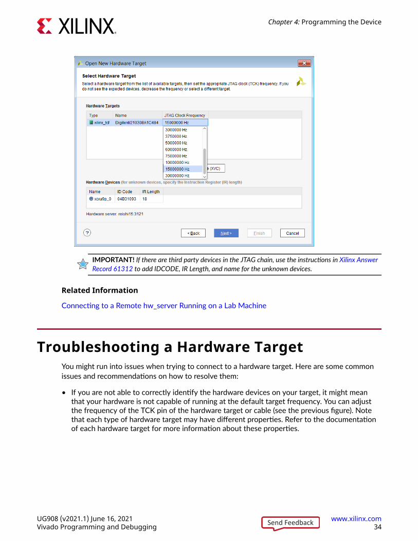
IMPORTANT! If there are third party devices in the JTAG chain, use the instructions in Xilinx AnswerRecord 61312 to add IDCODE, IR Length, and name for the unknown devices.
Related Information
Connecting to a Remote hw_server Running on a Lab Machine
Troubleshooting a Hardware TargetYou might run into issues when trying to connect to a hardware target. Here are some commonissues and recommendations on how to resolve them:
• If you are not able to correctly identify the hardware devices on your target, it might meanthat your hardware is not capable of running at the default target frequency. You can adjustthe frequency of the TCK pin of the hardware target or cable (see the previous figure). Notethat each type of hardware target may have different properties. Refer to the documentationof each hardware target for more information about these properties.
Chapter 4: Programming the Device
UG908 (v2021.1) June 16, 2021 www.xilinx.comVivado Programming and Debugging 34Send Feedback
• While the Vivado hardware server will attempt to automatically determine the instructionregister (IR) length of all devices in the JTAG chain, in some rare circumstances it might not beable to correctly do so. You should check the IR length for each unknown device to make sureit is correct. If you need to specify the IR length, you can do so directly in the HardwareDevices table of the Open New Hardware Target wizard (see Opening a New HardwareTarget).
Related Information
Opening a New Hardware Target
Opening a Recent Hardware TargetThe Open New Hardware Target wizard is also what populates a list of previously connectedhardware targets. Instead of connecting to a hardware target by going through the wizard, youcan re-open a connection to a previously connected hardware target by selecting the Openrecent target link in the Hardware Manager window and selecting one of the recently connectedhardware server/target combinations in the list. You can also access this list of recently usedtargets through the Open Target selection under Hardware Manager in the Program and Debugsection of the Vivado flow navigator.
Opening a Hardware Target Using Tcl CommandsYou can also use Tcl commands to connect to a hardware server/target combination. Forinstance, to connect to the digilent_plugin target (serial number 210203339395A) that ismanaged by the hw_server running on localhost 3121, use the following Tcl commands:
connect_hw_server -url localhost:3121current_hw_target [get_hw_targets */xilinx_tcf/Digilent/210203339395A]set_property PARAM.FREQUENCY 15000000 [get_hw_targets \ */xilinx_tcf/Digilent/210203339395A]open_hw_target
Once you finish opening a connection to a hardware target, the Hardware window is populatedwith the hardware server, hardware target, and various hardware devices for the open target (seethe following figure).
Chapter 4: Programming the Device
UG908 (v2021.1) June 16, 2021 www.xilinx.comVivado Programming and Debugging 35Send Feedback
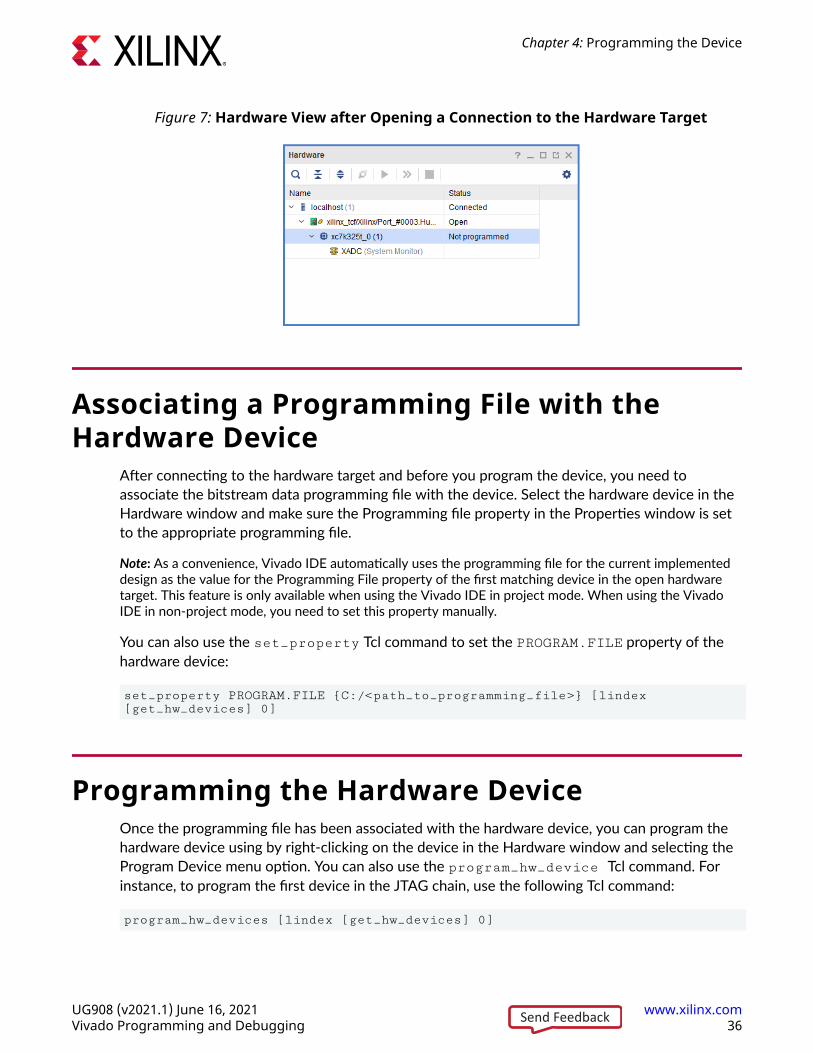
Figure 7: Hardware View after Opening a Connection to the Hardware Target
Associating a Programming File with theHardware Device
After connecting to the hardware target and before you program the device, you need toassociate the bitstream data programming file with the device. Select the hardware device in theHardware window and make sure the Programming file property in the Properties window is setto the appropriate programming file.
Note: As a convenience, Vivado IDE automatically uses the programming file for the current implementeddesign as the value for the Programming File property of the first matching device in the open hardwaretarget. This feature is only available when using the Vivado IDE in project mode. When using the VivadoIDE in non-project mode, you need to set this property manually.
You can also use the set_property Tcl command to set the PROGRAM.FILE property of thehardware device:
set_property PROGRAM.FILE {C:/<path_to_programming_file>} [lindex [get_hw_devices] 0]
Programming the Hardware DeviceOnce the programming file has been associated with the hardware device, you can program thehardware device using by right-clicking on the device in the Hardware window and selecting theProgram Device menu option. You can also use the program_hw_device Tcl command. Forinstance, to program the first device in the JTAG chain, use the following Tcl command:
program_hw_devices [lindex [get_hw_devices] 0]
Chapter 4: Programming the Device
UG908 (v2021.1) June 16, 2021 www.xilinx.comVivado Programming and Debugging 36Send Feedback
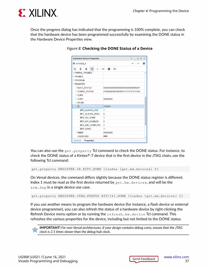
Once the progress dialog has indicated that the programming is 100% complete, you can checkthat the hardware device has been programmed successfully by examining the DONE status inthe Hardware Device Properties view.
Figure 8: Checking the DONE Status of a Device
You can also use the get_property Tcl command to check the DONE status. For instance, tocheck the DONE status of a Kintex®-7 device that is the first device in the JTAG chain, use thefollowing Tcl command:
get_property REGISTER.IR.BIT5_DONE [lindex [get_hw_devices] 0]
On Versal devices, the command differs slightly because the DONE status register is different.Index 1 must be read as the first device returned by get_hw_devices, and will be thearm_dap in a single device use case.
get_property REGISTER.JTAG_STATUS.BIT[34]_DONE [lindex [get_hw_devices] 1]
If you use another means to program the hardware device (for instance, a flash device or externaldevice programmer), you can also refresh the status of a hardware device by right-clicking theRefresh Device menu option or by running the refresh_hw_device Tcl command. Thisrefreshes the various properties for the device, including but not limited to the DONE status.
IMPORTANT! For non-Versal architectures, if your design contains debug cores, ensure that the JTAGclock is 2.5 times slower than the debug hub clock.
Chapter 4: Programming the Device
UG908 (v2021.1) June 16, 2021 www.xilinx.comVivado Programming and Debugging 37Send Feedback
IMPORTANT! User SCAN Chain: For non-Versal architectures, Vivado Programmer tries to detect debugcores on the user scan chain specified in the design by default. It does the detection by issuing aJTAG_CHAIN 1 command to the device. If you have programmed a device with a design that does nothave any debug cores or a debug core with a user scan chain of 2, 3, or 4, you will see a warning.
To determine the user scan chain setting, for non-Versal architectures, open the implementeddesign and use:
get_property C_USER_SCAN_CHAIN [get_debug_cores dbg_hub]
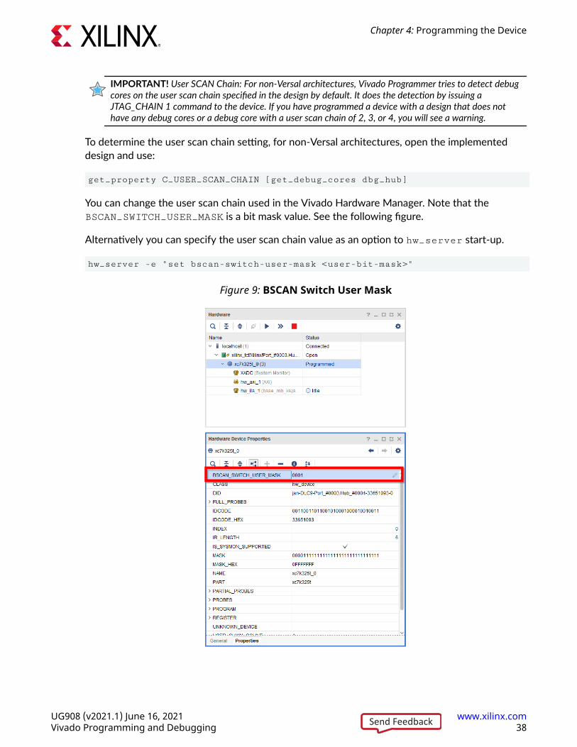
You can change the user scan chain used in the Vivado Hardware Manager. Note that theBSCAN_SWITCH_USER_MASK is a bit mask value. See the following figure.
Alternatively you can specify the user scan chain value as an option to hw_server start-up.
hw_server -e "set bscan-switch-user-mask <user-bit-mask>"
Figure 9: BSCAN Switch User Mask
Chapter 4: Programming the Device
UG908 (v2021.1) June 16, 2021 www.xilinx.comVivado Programming and Debugging 38Send Feedback
TIP: For designs prior to Vivado 2016.3 Xilinx recommends manually launching hw_server with -e "set xsdb-user-bscan <C_USER_SCAN_CHAIN scan_chain_number>" to detect thedebug hub at User Scan Chain of 2 or 4.
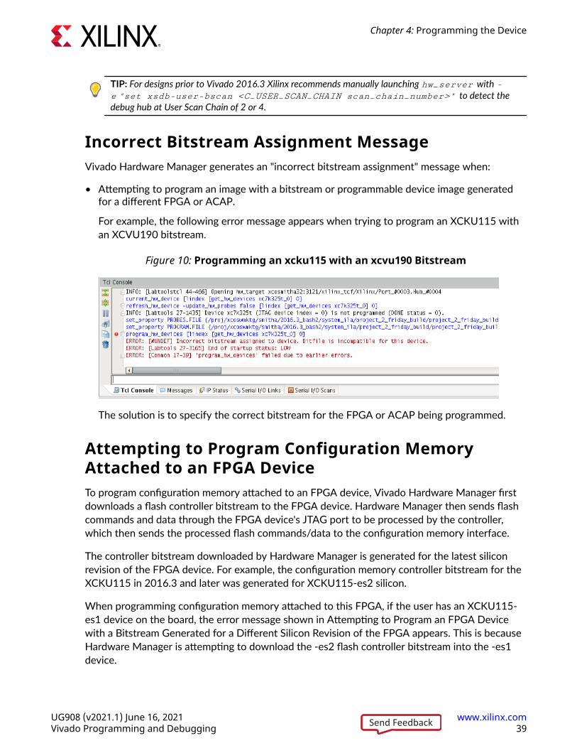
Incorrect Bitstream Assignment MessageVivado Hardware Manager generates an "incorrect bitstream assignment" message when:
• Attempting to program an image with a bitstream or programmable device image generatedfor a different FPGA or ACAP.
For example, the following error message appears when trying to program an XCKU115 withan XCVU190 bitstream.
Figure 10: Programming an xcku115 with an xcvu190 Bitstream
The solution is to specify the correct bitstream for the FPGA or ACAP being programmed.
Attempting to Program Configuration MemoryAttached to an FPGA DeviceTo program configuration memory attached to an FPGA device, Vivado Hardware Manager firstdownloads a flash controller bitstream to the FPGA device. Hardware Manager then sends flashcommands and data through the FPGA device's JTAG port to be processed by the controller,which then sends the processed flash commands/data to the configuration memory interface.
The controller bitstream downloaded by Hardware Manager is generated for the latest siliconrevision of the FPGA device. For example, the configuration memory controller bitstream for theXCKU115 in 2016.3 and later was generated for XCKU115-es2 silicon.
When programming configuration memory attached to this FPGA, if the user has an XCKU115-es1 device on the board, the error message shown in Attempting to Program an FPGA Devicewith a Bitstream Generated for a Different Silicon Revision of the FPGA appears. This is becauseHardware Manager is attempting to download the -es2 flash controller bitstream into the -es1device.
Chapter 4: Programming the Device
UG908 (v2021.1) June 16, 2021 www.xilinx.comVivado Programming and Debugging 39Send Feedback

Closing the Hardware TargetYou can close a hardware target by right-clicking on the hardware target in the Hardwarewindow and selecting Close Target from the popup menu. You can also close the hardware targetusing a Tcl command. For instance, to close the xilinx_platformusb/USB21 target on the localhostserver, use the following Tcl command:
close_hw_target {localhost/xilinx_tcf/Digilent/210203339395A}
IMPORTANT! If the board is powered off or cable disconnected, Vivado IDE closes the hardware target inthe Hardware Manager. Any Vivado operation in the main Vivado thread is also canceled. If the board ispowered back on or the cable is reconnected, the Vivado IDE will attempt to re-open the hardware targetin the Hardware Manager.
Closing a Connection to the Hardware ServerYou can close a hardware server by right-clicking on the hardware server in the Hardwarewindow and selecting Close Server from the popup menu. You can also close the hardwareserver using a Tcl command. For instance, to close the connection to the localhost server, use thefollowing Tcl command:
disconnect_hw_server localhost
IMPORTANT! If Vivado Hardware Manager is connected to the hw_server, and the hw_server is stopped,the Hardware Manager detects this condition automatically and disconnects from the server.
Reconnecting to a Target Device with a LowerJTAG Clock Frequency
The JTAG chain is as fast as the slowest device in the chain. Therefore, to lower the JTAG clockfrequency, connect to a target device whose JTAG clock frequency is less than the default JTAGclock frequency.
You should attempt to open with a default JTAG clock frequency that is 15 MHz for the Digilentcable connection and 6 MHz for the USB cable connection. If it is not possible to connect atthese speeds, Xilinx recommends that you lower the default JTAG clock frequency even furtheras described below.
Chapter 4: Programming the Device
UG908 (v2021.1) June 16, 2021 www.xilinx.comVivado Programming and Debugging 40Send Feedback
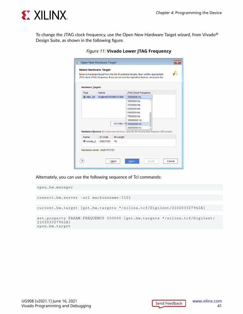
To change the JTAG clock frequency, use the Open New Hardware Target wizard, from Vivado®
Design Suite, as shown in the following figure.
Figure 11: Vivado Lower JTAG Frequency
Alternately, you can use the following sequence of Tcl commands:
open_hw_manager
connect_hw_server -url machinename:3121
current_hw_target [get_hw_targets */xilinx_tcf/Digilent/210203327962A]
set_property PARAM.FREQUENCY 250000 [get_hw_targets */xilinx_tcf/Digilent/210203327962A] open_hw_target
Chapter 4: Programming the Device
UG908 (v2021.1) June 16, 2021 www.xilinx.comVivado Programming and Debugging 41Send Feedback
Connecting to a Server with More Than 32Devices in a JTAG Chain
It is possible to connect to a server which has more than 32 devices in its JTAG chain in Vivado.You need to provide option max-jtag-devices at the startup of hw_server to enable theability to detect more devices in a scan chain. The default value for this setting is 32. Note thatincreasing this number will slow down the device discovery process which in turn can slow downcable access.
Specify the max-jtag-devices option at hw_server start-up as follows:
hw_server -e "set max-jtag-devices 64"
UsageThis option is used to start up the hw_server with the ability to enable ir lengths greater than 64bits. The default value for this setting is 64. You can increase this value for devices in the JTAGchains whose ir length are wider (for example 93). Note that increasing this number will slow thedevice discovery process, which in turn can slow cable access. Therefore, you should onlyincrease this value for systems with long ir lengths and device counts.
This is how you specify the option at hw_server start-up:
hw_server -e "set max-ir-length 93"
Init OptionYou may also use the --init=script.txt option to load this setting through a file. To use theinit option, create a initialization script as shown in the following example. In the script, specifythe set max-jtag-device parameter.
# Sample script.txtset max-ir-length 93
Start the hw_server as shown in the following example:
hw_server --init=script.txt
Chapter 4: Programming the Device
UG908 (v2021.1) June 16, 2021 www.xilinx.comVivado Programming and Debugging 42Send Feedback
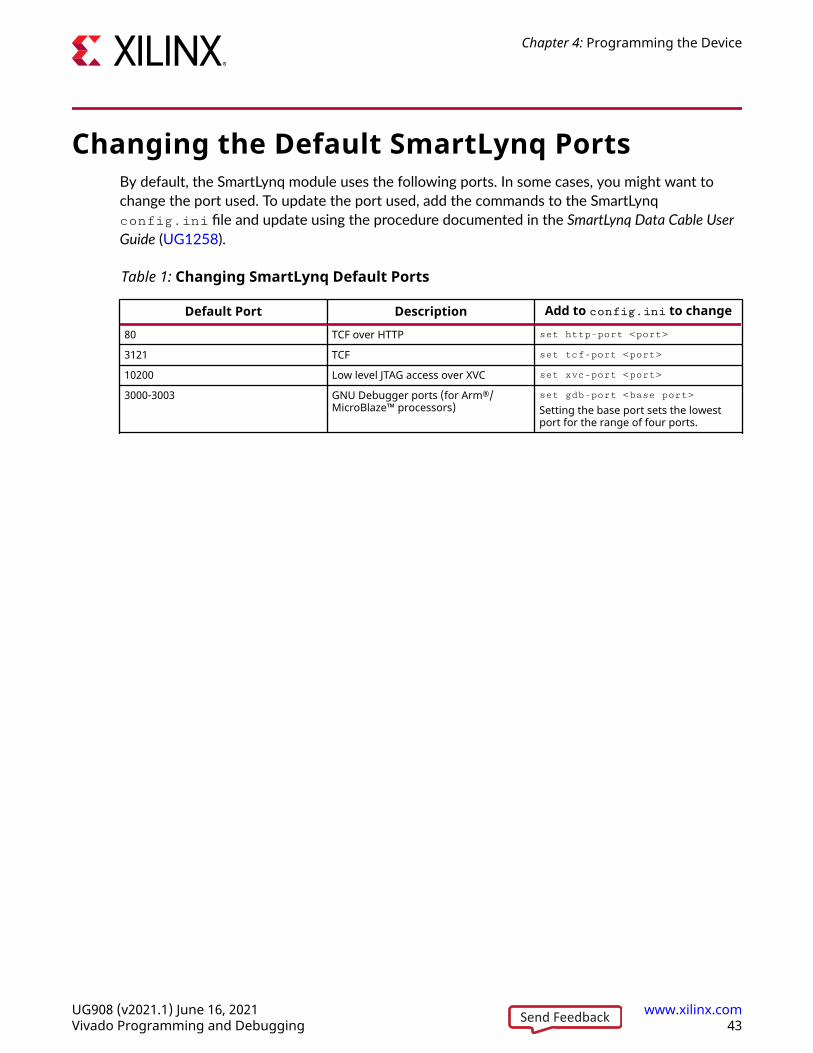
Changing the Default SmartLynq PortsBy default, the SmartLynq module uses the following ports. In some cases, you might want tochange the port used. To update the port used, add the commands to the SmartLynqconfig.ini file and update using the procedure documented in the SmartLynq Data Cable UserGuide (UG1258).
Table 1: Changing SmartLynq Default Ports
Default Port Description Add to config.ini to change
80 TCF over HTTP set http-port <port>
3121 TCF set tcf-port <port>
10200 Low level JTAG access over XVC set xvc-port <port>
3000-3003 GNU Debugger ports (for Arm®/MicroBlaze™ processors)
set gdb-port <base port>
Setting the base port sets the lowestport for the range of four ports.
Chapter 4: Programming the Device
UG908 (v2021.1) June 16, 2021 www.xilinx.comVivado Programming and Debugging 43Send Feedback

Chapter 5
Remote Debugging in VivadoThe need for remote debugging may arise in a variety of situations. It could be required in theprototyping phase of a product, where you might want to debug a design in the lab withoutphysical access to the lab, or where you might want to share resources across your organization.Remote debugging could also be required to perform in-the-field debug to diagnose issues orextend product life cycle.
Xilinx® provides multiple solutions to debug your design remotely. This can be done using theXilinx Hardware Server product to connect to a remote computer in the lab. You could alsoimplement the Xilinx Virtual Cable (XVC) protocol to connect to a network-connected board.Each of these solutions are explained in detail in the sections below.
Using Vivado Hardware Server to Debug OverEthernet
You can connect to a remote lab machine using Vivado Hardware Server product. This is a smallsized (<100 MB) standalone download available for install on the lab machine. This optionrequires intranet or internet access and can be used internally just within your organization aswell.
Figure 12: Debug via Internet/Intranet Using Hardware Server
Desk Lab
INTERNET / INTRANET
HARDWARE SERVER
X14741-062315
Chapter 5: Remote Debugging in Vivado
UG908 (v2021.1) June 16, 2021 www.xilinx.comVivado Programming and Debugging 44Send Feedback

Xilinx Virtual Cable (XVC) for 7 Series,UltraScale, and UltraScale+ FPGAs andMPSoCs
Vivado IDE supports the Xilinx Virtual Cable (XVC) protocol. Xilinx Virtual Cable lets you accessand debug a Xilinx device without using a USB or parallel configuration cable. This capabilityhelps facilitate Vivado IDE to debug for designs that:
• Have the FPGA in a hard-to-access location, where a "lab-PC" is not convenient.
• Do not have direct access to the device pins on the board - for example, if the JTAG pins areonly accessible with a local microprocessor interface.
IMPORTANT! Note that Xilinx Virtual Cable is not supported for Versal architectures.
XVC is an internet-based (TCP/IP) protocol that acts like a JTAG cable. It has very basic cablecommands. This allows XVC to debug a system over an intranet, or even the internet. With thiscapability you can save on costly or impractical travel and reduce the time it takes to debug aremote system.
Another common use of XVC is for shared systems that are not co-located with teams that needaccess to them. It can also be used when there are physical constraints to using the system, suchas when the JTAG connector is not available or accessible. XVC implementation is programminglanguage and platform independent.
Rather than using a dedicated JTAG header, an existing Ethernet connection can be used tocreate the appropriate JTAG commands from a processor to a target device. With the XVC v1.0Protocol, Vivado can communicate the same JTAG commands over an Ethernet connection andstill support all of the existing Vivado debug features.
IMPORTANT! If the Vivado Debug Bridge IP is used for XVC, Vivado IDE does not support programmingfeatures. The assumption is that the device is programmed before using XVC to debug the design. TheDebug Bridge IP is not compatible with Versal ACAP.
Vivado Debug Bridge IP and Xilinx Virtual Cable(XVC) FlowNote: Vivado Debug Bridge IP is not supported on Versal™ devices.
Chapter 5: Remote Debugging in Vivado
UG908 (v2021.1) June 16, 2021 www.xilinx.comVivado Programming and Debugging 45Send Feedback
The Vivado Debug Bridge IP core is a controller that provides multiple options to communicatewith the debug cores in the design. This design can be a flat design or a Dynamic FunctioneXchange design. In addition, the Debug Bridge IP core can also be configured to take advantageof debugging designs using a JTAG cable or remotely through Ethernet, PCIe®, or otherinterfaces without the need for a JTAG cable.
Different modes in Debug Bridge IP facilitate the support of various use cases.
Debug Bridge in XVC Modes
There are five modes in the Debug Bridge that are used in Xilinx Virtual Cable (XVC)implementations.
• From AXI to BSCAN: In this mode, the Debug Bridge receives XVC Commands via AXI4-Liteslave interface.
• From JTAG to BSCAN: In this mode, the Debug Bridge receives XVC Commands via JTAGslave interface driven by user logic.
• From PCIe to BSCAN: In this mode, the Debug Bridge receives XVC Commands via PCIeExtended Configuration slave interface.
• From PCIe to JTAG: In this mode, the Debug Bridge receives XVC Commands via PCIeExtended Configuration interface. This Debug Bridge brings out the JTAG pins out of theFPGA through I/O pins. This mode is mainly used to debug design on another board overXVC.
• From AXI to JTAG: In this mode, the Debug Bridge receives XVC commands via AXI4-Liteinterface to send over the JTAG pins to a target device.
In all of these modes the Debug Bridge can further communicate with other debug cores/ DebugBridge instances in the design via the Soft-BSCAN (Boundary Scan) interface. The Soft BSCANmaster interface enables extension of the JTAG interface to internal USER defined scan chains/Debug Bridge instances.
Using Debug Bridge IP in Dynamic Function eXchange Designs
The Debug Bridge IP can be used in both flat and Dynamic Function eXchange designs. Beloware the details on the Debug Bridge configurations used in the static or Reconfigurable Partition(RP) region of a Dynamic Function eXchange design. Multiple Debug Bridge instances arepermitted in a partition depending on the design requirements.
• BSCAN Primitive: This mode is used when a Debug Bridge containing a BSCAN primitive isrequired in the static region. The BSCAN master interface of this Debug Bridge can beconnected to another Debug Bridge instance in the static and/or PR region(s) providing one ormore communication pathways for debugging those regions.
Chapter 5: Remote Debugging in Vivado
UG908 (v2021.1) June 16, 2021 www.xilinx.comVivado Programming and Debugging 46Send Feedback
• From BSCAN to Debug Hub: In this mode, the Debug Bridge uses the BSCAN slave interfaceto communicate to Vivado Hardware Manager. It uses the Debug Hub interface tocommunicate with the design cores within the relevant static or RP region. You can alsooptionally add additional BSCAN Masters to the output of this Debug Bridge, which enablesdebugging other debug cores like MicroBlaze Debug Module (MDM) or other Debug Bridgeinstances.
Note: The tool automatically connects the debug cores in an RP to the Debug Bridge if this is the onlyDebug Bridge instantiated in the partition.
• From AXI to BSCAN: In this mode, the Debug Bridge receives XVC Commands via AXI4-Liteslave interface. This Debug Bridge can further communicate with other debug cores/ DebugBridge instances in the design via the Soft-BSCAN (Boundary Scan) master interface. The SoftBSCAN interface enables extension of the JTAG interface to internal USER defined scanchains/Debug Bridge instances.
• From JTAG to BSCAN: In this mode, the Debug Bridge receives XVC Commands via JTAGslave interface driven by user logic. This Debug Bridge can further communicate with otherdebug cores/ Debug Bridge instances in the design via the Soft-BSCAN (Boundary Scan)master interface. The Soft BSCAN interface enables extension of the JTAG interface tointernal USER defined scan chains/Debug Bridge instances.
• From PCIe to BSCAN: In this mode, the Debug Bridge receives XVC Commands via PCIeExtended Configuration slave interface. This Debug Bridge can further communicate withother debug cores/ Debug Bridge instances in the design via the Soft-BSCAN (Boundary Scan)interface. The Soft BSCAN master interface enables extension of the JTAG interface tointernal USER defined scan chains/Debug Bridge instances.
Note: This mode is only available for UltraScale+ and UltraScale device architectures
• From PCIe to JTAG: In this mode, the Debug Bridge receives XVC Commands via PCIeExtended Configuration interface. This Debug Bridge brings out the JTAG pins out of theFPGA through I/O pins. This mode is mainly used to debug design on another board overXVC.
Note: This mode is only available for UltraScale+ and UltraScale device architectures.
• From AXI to JTAG: In this mode, the Debug Bridge receives XVC commands via AXI4-Liteinterface to send over the JTAG pins to a target device.
JTAG Fallback Support
The XVC based debug solution can be used with AXI masters such as the PCIe XDMA IP. If theAXI master is in a hang situation or is otherwise not functioning properly, there are no methodsto debug those scenarios. To provide a JTAG-based fall back debug pathway that is parallel to theXVC pathway, Xilinx recommends using the Debug Bridge in BSCAN Primitive mode. A DebugBridge in BSCAN Primitive mode can be instantiated in static region and its BSCAN masterinterface can be connected to the BSCAN slave interface of a second Debug Bridge that isconfigured with the JTAG Fallback Support enabled. There are two JTAG Fallback Support types:
Chapter 5: Remote Debugging in Vivado
UG908 (v2021.1) June 16, 2021 www.xilinx.comVivado Programming and Debugging 47Send Feedback
1. If the Debug Bridge that you want to provide JTAG Fallback for resides in a PR region, youneed to enable the External BSCAN Master JTAG Fallback Support.
2. If the Debug Bridge that you want to provide JTAG Fallback for resides in the static region (orin a flat design), you should enable the Internal BSCAN Master JTAG Fallback Support.
Microblaze Debug Module (MDM) Support
Debug access to Microblaze Debug Module (MDM) is also supported by the Debug Bridge. TheMDM BSCAN slave input can be connected to any Debug Bridge configuration mode thatsupports multiple BSCAN master interfaces at the output (for example, AXI to BSCAN with itsBSCAN Master Count greater than zero).
Multiple Debug Trees
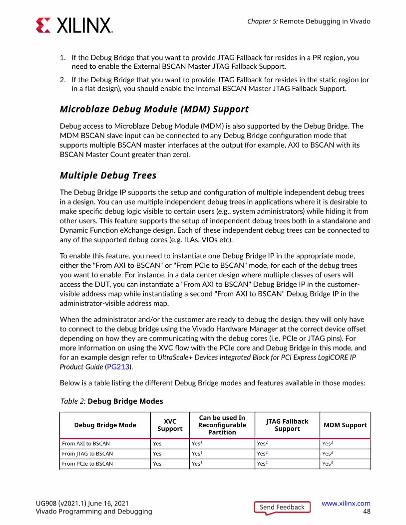
The Debug Bridge IP supports the setup and configuration of multiple independent debug treesin a design. You can use multiple independent debug trees in applications where it is desirable tomake specific debug logic visible to certain users (e.g., system administrators) while hiding it fromother users. This feature supports the setup of independent debug trees both in a standalone andDynamic Function eXchange design. Each of these independent debug trees can be connected toany of the supported debug cores (e.g. ILAs, VIOs etc).
To enable this feature, you need to instantiate one Debug Bridge IP in the appropriate mode,either the "From AXI to BSCAN" or "From PCIe to BSCAN" mode, for each of the debug treesyou want to enable. For instance, in a data center design where multiple classes of users willaccess the DUT, you can instantiate a "From AXI to BSCAN" Debug Bridge IP in the customer-visible address map while instantiating a second "From AXI to BSCAN" Debug Bridge IP in theadministrator-visible address map.
When the administrator and/or the customer are ready to debug the design, they will only haveto connect to the debug bridge using the Vivado Hardware Manager at the correct device offsetdepending on how they are communicating with the debug cores (i.e. PCIe or JTAG pins). Formore information on using the XVC flow with the PCIe core and Debug Bridge in this mode, andfor an example design refer to UltraScale+ Devices Integrated Block for PCI Express LogiCORE IPProduct Guide (PG213).
Below is a table listing the different Debug Bridge modes and features available in those modes:
Table 2: Debug Bridge Modes
Debug Bridge Mode XVCSupport
Can be used InReconfigurable
PartitionJTAG Fallback
Support MDM Support
From AXI to BSCAN Yes Yes1 Yes2 Yes3
From JTAG to BSCAN Yes Yes1 Yes2 Yes3
From PCIe to BSCAN Yes Yes1 Yes2 Yes3
Chapter 5: Remote Debugging in Vivado
UG908 (v2021.1) June 16, 2021 www.xilinx.comVivado Programming and Debugging 48Send Feedback
Table 2: Debug Bridge Modes (cont'd)
Debug Bridge Mode XVCSupport
Can be used InReconfigurable
PartitionJTAG Fallback
Support MDM Support
From PCIe to JTAG Yes Yes1 NA NA
From BSCAN to DebugHub No Yes1 NA Yes3
BSCAN Primitive No No NA Yes3
From AXI to JTAG Yes Yes NA NA
Notes:1. BSCAN Master Count can be greater than 0 and can be connected to other Debug Bridge instances or
MicroBlaze/MDM core within the same RP only.2. Internal BSCAN Mode can only be used when the Debug Bridge is in static partition while External BSCAN Mode can
be used when the Debug Bridge is in either the static or RPs.3. BSCAN Master Count can be greater than 0 and can be connected to other Debug Bridge instances or
MicroBlaze/MDM core within the same RP only.
Below is an illustration of a design with the XVC Debug Bridge in an RP.
Figure 13: Dynamic Function eXchange Design with the XVC Debug Bridge in an RP
This is a PR design with two reconfigurable partitions, Counter RP and Shifter RPs. This figureillustrates the different Debug Bridge modes used in both static and RP regions.
Chapter 5: Remote Debugging in Vivado
UG908 (v2021.1) June 16, 2021 www.xilinx.comVivado Programming and Debugging 49Send Feedback
The static partition of design has two Debug Bridge IPs. The first Debug Bridge IP is in BSCANPrimitive mode and configured to have three BSCAN master interfaces. Two of the BSCANmaster interfaces are connected to the Debug Bridge instances in Counter-RP and Shifter-RPpartitions providing a parallel path for debug. The third BSCAN master interface is connected toanother Debug Bridge instance within the static partition configured in the From BSCAN toDebug Hub mode. The Debug Bridge configured in From BSCAN to Debug Hub mode cancommunicates to the various Debug IPs (ILA, VIO, JTAG-to-AXI, etc.) in the design, which in thiscase is the ILA IP.
In this system the Counter-RP partition contains a Debug Bridge instantiated in the AXI-to-BSCAN mode. You can use this Debug Bridge in XVC mode, the Debug Bridge receives XVCCommands via AXI4-Lite interface. This Debug Bridge can further communicate with otherDebug Bridge instances in the design via the Soft-BSCAN (Boundary Scan) interface. Since thisDebug Bridge is configured to contain two BSCAN master interfaces it communicates with theMDM and the Debug Bridge instance configured in From BSCAN to Debug Hub mode. TheDebug Bridge configured in From BSCAN to Debug Hub mode can communicates to the variousDebug IPs (ILA, VIO, JTAG-to-AXI etc.) in the design, which in this case is the ILA IP.
On the other hand, the Shifter-RP partition contains only one Debug Bridge instance configuredin From BSCAN to Debug Hub mode that can communicate with the various Debug IPs (ILA, VIO,JTAG-to-AXI etc.) in the design, which in this case is the ILA IP.
For more information see the Debug Bridge LogiCORE IP Product Guide (PG245).
An illustration of some of the Debug Bridge modes is presented below.
From AXI to BSCANThis bridge type is intended for designs using Xilinx Virtual Cable (XVC) to remotely debug anFPGA or SoC device through Ethernet or other interfaces without the need for JTAG cable. Inthis mode, the Debug Bridge expects to receive Xilinx Virtual Cable commands via AXI4-Liteinterface. Use this mode to debug designs on the FPGA device over the Xilinx Virtual Cable.
For more information, see the Debug Bridge LogiCORE IP Product Guide (PG245).
Chapter 5: Remote Debugging in Vivado
UG908 (v2021.1) June 16, 2021 www.xilinx.comVivado Programming and Debugging 50Send Feedback
Figure 14: AXI to BSCAN Debug Bridge
Data Center
XVC over TCP/IP
hw_server
ZynqProcessor
XVC Server AXI
Debug Bridge
(From AXI to BSCAN)
BSCAN
User Solution
Vivado Solution
Target Board/FPGA
Debug Hub
Debug IP 1 (eg ILA, VIO etc)……Debug IP n (eg ILA, VIO etc)
X17961-092816
From PCIe to BSCANIn a typical PCIe setup - you can use the Debug Bridge in the PCIe to BSCAN mode tocommunicate with the debug cores. In this mode, Debug Bridge connects to the ExtendedConfiguration Interface of the PCIe IP. This is a common data center use case where PCIe is thepreferred communication pathway to the Host PC instead of JTAG. For more information onusing the XVC flow with the PCIe core and Debug Bridge in this mode, and for an example designrefer to UltraScale+ Devices Integrated Block for PCI Express LogiCORE IP Product Guide (PG213).
Figure 15: PCIe to BSCAN Debug Bridge Used with PCIe Extended ConfigurationInterface
ProcessorXVC Server
PCIe
hw_server
XVC overTCP/IP
PCIe(Extended
Configuration) PCIe extcfg
Debug Bridge
(From AXI to BSCAN)
BSCAN
User Solution
Vivado Solution
Target FPGA
Debug Hub
Debug Core 1 ……
Debug Core n
X17962-040517
From JTAG to BSCANThis bridge type is intended for designs that use Xilinx Virtual Cable (XVC) to remotely debug anFPGA or SoC device through Ethernet or other interfaces without the need for JTAG cable. Inthis mode, the Debug Bridge expects to receive XVC commands via JTAG interface driven byuser logic. For more information see the Debug Bridge LogiCORE IP Product Guide (PG245).
Chapter 5: Remote Debugging in Vivado
UG908 (v2021.1) June 16, 2021 www.xilinx.comVivado Programming and Debugging 51Send Feedback
Figure 16: JTAG to BSCAN Debug Bridge
Target Board
Data Center
ProcessorXVC Server GPIO/Custom
Interface
hw_server
User LogicJTAG
Debug Bridge
(From JTAG to BSCAN)
BSCAN
User Solution
Vivado Solution
Target FPGA
Debug Hub
Debug IP 1 (eg ILA, VIO etc)……Debug IP n (eg ILA, VIO etc)
XVC overTCP/IP
X17963-092816
From PCIe to JTAGIn a PCIe setup, you can use the Debug Bridge in the PCIe to JTAG mode to communicate withthe debug cores. In this mode, Debug Bridge connects to the Extended Configuration Interface ofthe PCIe® IP, which in turn can communicate over JTAG to the debug hub on a different targetFPGA.
Figure 17: PCIe® to JTAG Debug Bridge Used with PCIe Extended ConfigurationInterface
Target Board
PCIeMaster PCIe ext
cfg
hw_server
PCIe
Debug Bridge
(From PCIe to JTAG)
Debug Hub
User Responsibility
Vivado Solution
FPGA #2
JTAG
FPGA #1
Debug Core 1 ……
Debug Core n
X17964-040517
From AXI to JTAGThis bridge type is intended for designs that use Xilinx Virtual Cable (XVC) to remotely debug anFPGA or SoC device through Ethernet or other interfaces. In this mode, the Debug Bridgereceives XVC commands via AXI4-Lite interface to send over the JTAG pins to a target device.For more information see the Debug Bridge LogiCORE IP Product Guide (PG245).
Chapter 5: Remote Debugging in Vivado
UG908 (v2021.1) June 16, 2021 www.xilinx.comVivado Programming and Debugging 52Send Feedback
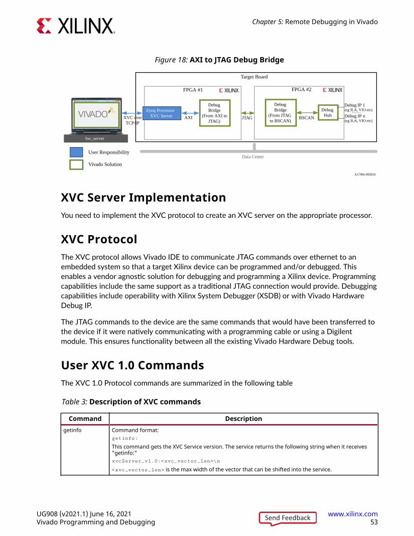
Figure 18: AXI to JTAG Debug Bridge
Target Board
Data Center
Zynq ProcessorXVC Server AXI
hw_server
XVC overTCP/IP
Debug Bridge
(From AXI to JTAG)
BSCAN
Debug Hub
User Responsibility
Vivado Solution
FPGA #2
JTAG
Debug Bridge
(From JTAG to BSCAN)
FPGA #1
Debug IP 1 (eg ILA, VIO etc)……Debug IP n (eg ILA, VIO etc)
X17966-092816
XVC Server ImplementationYou need to implement the XVC protocol to create an XVC server on the appropriate processor.
XVC ProtocolThe XVC protocol allows Vivado IDE to communicate JTAG commands over ethernet to anembedded system so that a target Xilinx device can be programmed and/or debugged. Thisenables a vendor agnostic solution for debugging and programming a Xilinx device. Programmingcapabilities include the same support as a traditional JTAG connection would provide. Debuggingcapabilities include operability with Xilinx System Debugger (XSDB) or with Vivado HardwareDebug IP.
The JTAG commands to the device are the same commands that would have been transferred tothe device if it were natively communicating with a programming cable or using a Digilentmodule. This ensures functionality between all the existing Vivado Hardware Debug tools.
User XVC 1.0 CommandsThe XVC 1.0 Protocol commands are summarized in the following table
Table 3: Description of XVC commands
Command Descriptiongetinfo Command format:
getinfo:
This command gets the XVC Service version. The service returns the following string when it receives"getinfo:"xvcServer_v1.0:<xvc_vector_len>\n
<xvc_vector_len> is the max width of the vector that can be shifted into the service.
Chapter 5: Remote Debugging in Vivado
UG908 (v2021.1) June 16, 2021 www.xilinx.comVivado Programming and Debugging 53Send Feedback
Table 3: Description of XVC commands (cont'd)
Command Descriptionshift Command format:
shift:[num bits][tms vector][tdi vector]
This command shifts in num_bits using the byte vectors tms_vector and tdi_vectornum_bits is an integer in little-endian mode.This represents the number of TCK clk toggles needed to shift the vectors out.tms_vector is a byte sized vector with all the TMS shift bits.Bit 0 in Byte 0 of this vector is shifted out first.The vector is num_bits and rounds up to the nearest byte.tdi_vector is like tms_vector but this represents all the tdi vectors to be shifted in.This command returns a byte vector of the same size as tms_vector with the corresponding tdo bitssampled for every bit shifted in.Bit 0 in Byte 0 of this vector is the first tdo value read from the shift
settck Command format:settck:[period]
This command attempts to set the service tck period to [period].[period] is specified in ns.This is a little-endian integer valueThis command returns the applied period when it completes settck:.Returned value is specified in ns.This is a little-endian integer value
Initializing Vivado IDE hw_serverWhen Vivado IDE hw_server is initialized with an XVC connection Vivado IDE discovers the XVCcable just like any USB cable. To do that, start the Vivado IDE hw_server with these arguments
hw_server -e "set auto-open-servers xilinx-xvc:localhost:10200"
The auto-open-servers option enables the XVC cable to be initialized by hw_server at startup. You can initialize the hardware server to force a connection to an existing XVC cable. Theserver will automatically discover the XVC cables in future connections.
The argument to auto-open-servers is as follows
xilinx-xvc:<xvc_host_name>:<xvc_port>
Multiple servers can be specified using comma separated strings. When the hardware serverstarts, it attempts to establish connections to the specified XVC servers. Alternatively you canprovide the XVC server details when connecting to the target using the Vivado HardwareManager Open New Hardware Target wizard as shown in the following figure.
Chapter 5: Remote Debugging in Vivado
UG908 (v2021.1) June 16, 2021 www.xilinx.comVivado Programming and Debugging 54Send Feedback
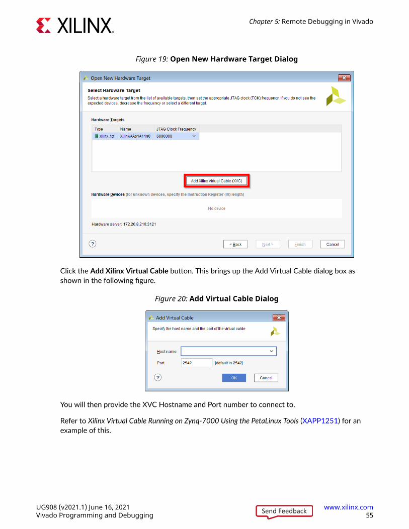
Figure 19: Open New Hardware Target Dialog
Click the Add Xilinx Virtual Cable button. This brings up the Add Virtual Cable dialog box asshown in the following figure.
Figure 20: Add Virtual Cable Dialog
You will then provide the XVC Hostname and Port number to connect to.
Refer to Xilinx Virtual Cable Running on Zynq-7000 Using the PetaLinux Tools (XAPP1251) for anexample of this.
Chapter 5: Remote Debugging in Vivado
UG908 (v2021.1) June 16, 2021 www.xilinx.comVivado Programming and Debugging 55Send Feedback
This application note shows how to get a Xilinx Virtual Cable (XVC) server running on aZynq®-7000 device with a Linux operating system generated with the PetaLinux Tools. Areference design is provided for the Avnet MicroZed board. The target device in this applicationnote is on an AC701 board and will be programmed and debugged by the MicroZed boardrunning XVC on Linux.
Note: For an example XVC server implementation over TCP/IP, refer to the following github repository: https://github.com/Xilinx/XilinxVirtualCable.
Chapter 5: Remote Debugging in Vivado
UG908 (v2021.1) June 16, 2021 www.xilinx.comVivado Programming and Debugging 56Send Feedback

Chapter 6
Programming ConfigurationMemory Devices
The Vivado® device programmer feature enables you to directly program Xilinx® FPGA devicesvia JTAG. Vivado can also indirectly program select Flash-based configuration memory devicesvia JTAG. Do this by first programming the Xilinx FPGA device with a special configuration thatprovides a data path between JTAG and the Flash device interface followed by programming theconfiguration memory device contents using this data path.
The Vivado device configuration feature enables you to directly configure Xilinx FPGAs orMemory Devices using either Xilinx or Digilent cables. See Connecting to a Hardware TargetUsing hw_server for a list of appropriate cables. Operating in Boundary-Scan mode, Vivado canconfigure or program Xilinx FPGAs, and Configuration Memory Devices.
Refer to JTAG Cables and Devices Supported by hw_server for a complete list of configurationmemory devices supported by Vivado.
To program and boot from a Configuration Memory Device in Vivado follow the steps below.
1. Generate bitstreams for use with configuration memory devices.
2. Create a Configuration Memory File (.mcs or .bin).
3. Connect to the Hardware target in Vivado.
4. Add the configuration memory device.
5. Program the configuration memory device using the Vivado IDE.
6. Boot the FPGA device (optional).
Related Information
Connecting to a Hardware Target Using hw_serverConfiguration Memory Support
Chapter 6: Programming Configuration Memory Devices
UG908 (v2021.1) June 16, 2021 www.xilinx.comVivado Programming and Debugging 57Send Feedback
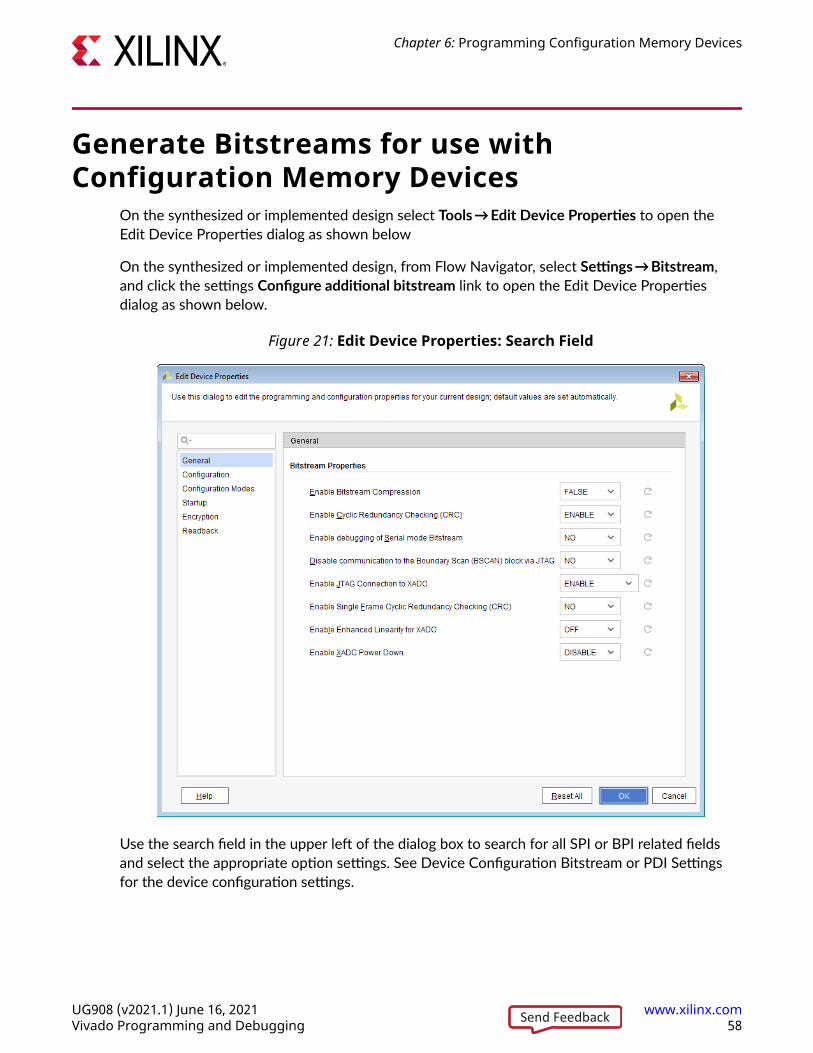
Generate Bitstreams for use withConfiguration Memory Devices
On the synthesized or implemented design select Tools → Edit Device Properties to open theEdit Device Properties dialog as shown below
On the synthesized or implemented design, from Flow Navigator, select Settings → Bitstream,and click the settings Configure additional bitstream link to open the Edit Device Propertiesdialog as shown below.
Figure 21: Edit Device Properties: Search Field
Use the search field in the upper left of the dialog box to search for all SPI or BPI related fieldsand select the appropriate option settings. See Device Configuration Bitstream or PDI Settingsfor the device configuration settings.
Chapter 6: Programming Configuration Memory Devices
UG908 (v2021.1) June 16, 2021 www.xilinx.comVivado Programming and Debugging 58Send Feedback
Related Information
Device Configuration Bitstream or PDI Settings
Creating a Configuration Memory File (forpre-Versal Devices Only)
Use the write_cfgmem Tcl command to create the .mcs or .bin programming file. This file willbe used in programming the configuration memory device.
For example, to generate an .mcs file for a single 1 Gbit BPI configuration memory device:
write_cfgmem -format mcs -interface bpix16 -size 128 \ -loadbit "up 0x0 design.bit"-file design.mcs
Note: The -size argument to write_cfgmem is in megabytes, different from flash device capacity whichis based on megabits. Hence, a 1 Gbit sized flash device is provided as 128 megabytes to write_cfgmemin the example above. Note that write_cfgmem automatically sizes the configuration memory file to thesize of the bitstream.
Vivado IDE supports the ability to chain multiple .bit files together using the write_cfgmemcommand. To generate an .mcs file for a single 1 Gbit BPI configuration memory devicecontaining multiple bitstreams:
write_cfgmem -format mcs -interface bpix16 -size 128 \ -loadbit "up 0 design1.bit up 0xFFFFF design2.bit" \ -file design1_design2.mcs
For more information on write_cfgmem command refer to the Vivado Design Suite Tcl CommandReference Guide (UG835).
TIP: You can create configuration memory files in Vivado Lab Edition.
You can also create the Configuration Memory file in Vivado IDE. Click on Tools → GenerateMemory Configuration File. This will bring up the Write Memory Configuration File dialog box asshown below.
Chapter 6: Programming Configuration Memory Devices
UG908 (v2021.1) June 16, 2021 www.xilinx.comVivado Programming and Debugging 59Send Feedback
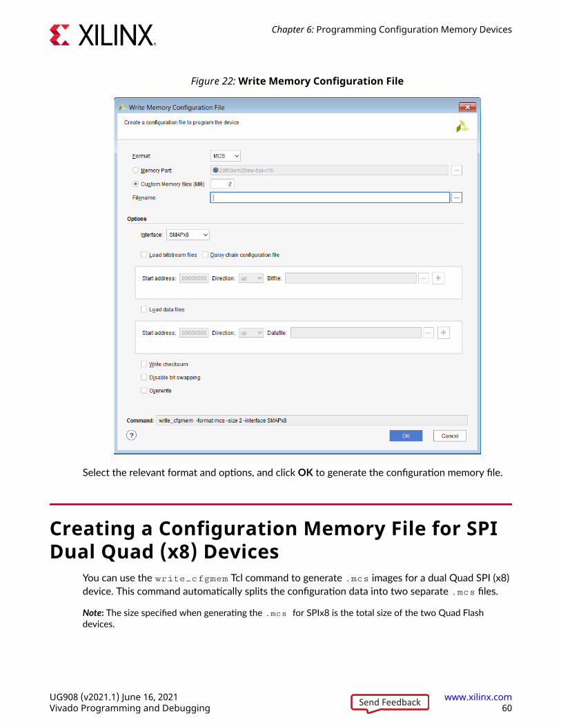
Figure 22: Write Memory Configuration File
Select the relevant format and options, and click OK to generate the configuration memory file.
Creating a Configuration Memory File for SPIDual Quad (x8) Devices
You can use the write_cfgmem Tcl command to generate .mcs images for a dual Quad SPI (x8)device. This command automatically splits the configuration data into two separate .mcs files.
Note: The size specified when generating the .mcs for SPIx8 is the total size of the two Quad Flashdevices.
Chapter 6: Programming Configuration Memory Devices
UG908 (v2021.1) June 16, 2021 www.xilinx.comVivado Programming and Debugging 60Send Feedback
Note: The write_cfgmem Tcl command divides the start address by 2 when building .mcs files for dualquad SPI (x8) mode.
Example write_cfgmem UsageThis example shows how to generate the .mcs files for a multiboot design with the "golden"bitstream loaded at address 0 and the multiboot bitstream loaded at address 0x0100_0000.
Devices: 2x 256 Mib Quad SPI Flash devices: 256 Mib = 32 MiB
Total storage size: 2 * 32 MiB = 64 MiB
Load addresses:
Golden: 0 * 2 = 0
Multiboot: 0x0100_0000 * 2 = 0x0200_0000
write_cfgmem -format mcs -interface spix8 -size 32 \ -loadbit "up 0 ./design1_spix8.bit up 0x02000000 ./design2_spix8.bit" \ -file design1_design2_spix8.mcs
Connect to the Hardware Target in VivadoTo connect to a hardware target in Vivado, do the following:
1. Ensure the appropriate configuration mode (Master SPI or Master BPI) is selected on theFPGA mode pins of the hardware target to configure the FPGA from a configuration memorydevice.
For more information, see the appropriate Configuration User Guide for the device you aretargeting.
2. Follow the steps in Programming the FPGA Device to connect to the hardware target.
IMPORTANT! If the board is powered off or cable disconnected, Vivado IDE closes the hardwaretarget. Any Vivado operation in the main Vivado thread is also canceled.
Related Information
Programming the Device
Chapter 6: Programming Configuration Memory Devices
UG908 (v2021.1) June 16, 2021 www.xilinx.comVivado Programming and Debugging 61Send Feedback
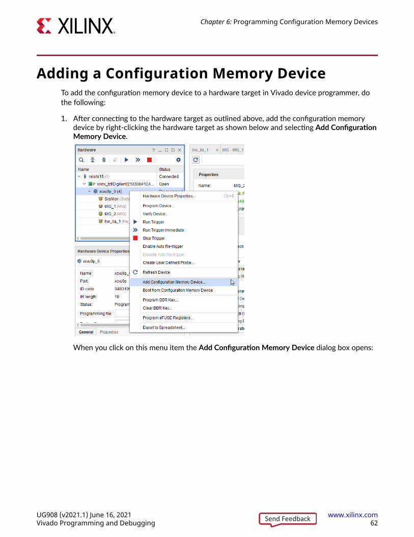
Adding a Configuration Memory DeviceTo add the configuration memory device to a hardware target in Vivado device programmer, dothe following:
1. After connecting to the hardware target as outlined above, add the configuration memorydevice by right-clicking the hardware target as shown below and selecting Add ConfigurationMemory Device.
When you click on this menu item the Add Configuration Memory Device dialog box opens:
Chapter 6: Programming Configuration Memory Devices
UG908 (v2021.1) June 16, 2021 www.xilinx.comVivado Programming and Debugging 62Send Feedback
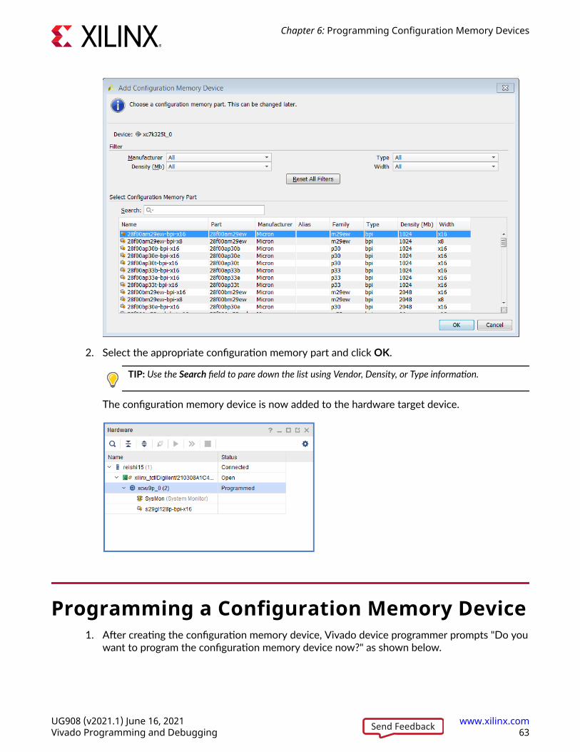
2. Select the appropriate configuration memory part and click OK.
TIP: Use the Search field to pare down the list using Vendor, Density, or Type information.
The configuration memory device is now added to the hardware target device.
Programming a Configuration Memory Device1. After creating the configuration memory device, Vivado device programmer prompts "Do you
want to program the configuration memory device now?" as shown below.
Chapter 6: Programming Configuration Memory Devices
UG908 (v2021.1) June 16, 2021 www.xilinx.comVivado Programming and Debugging 63Send Feedback
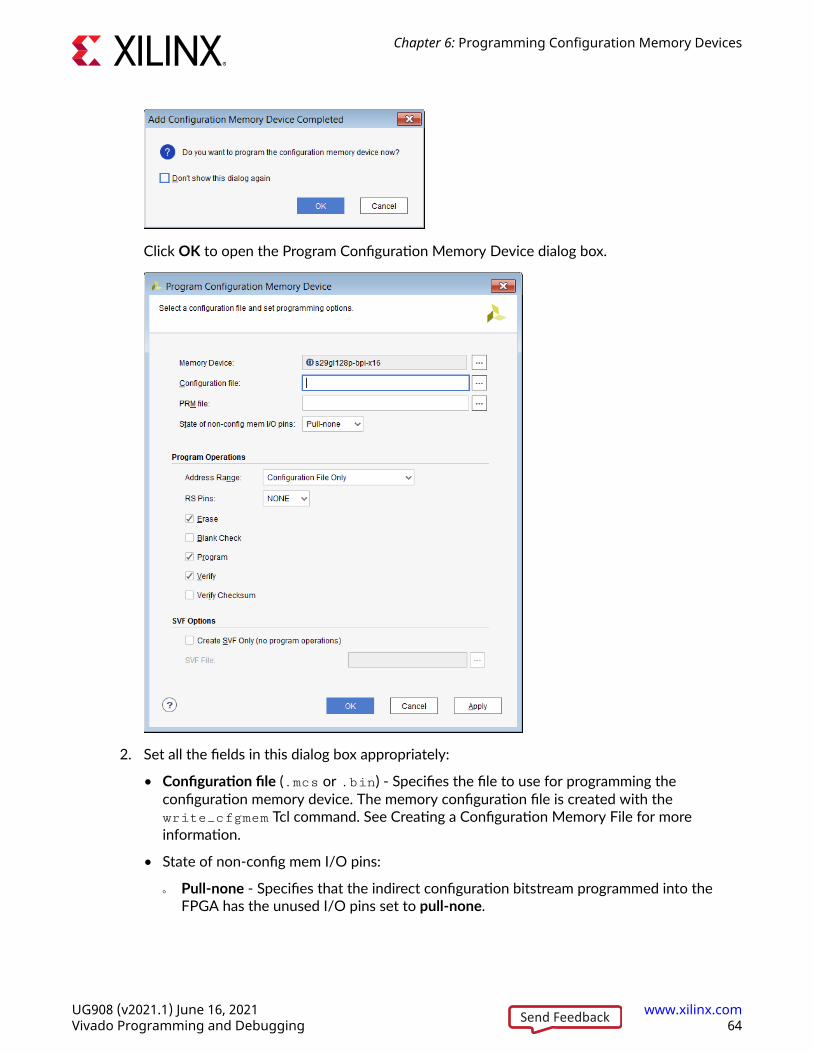
Click OK to open the Program Configuration Memory Device dialog box.
2. Set all the fields in this dialog box appropriately:
• Configuration file (.mcs or .bin) - Specifies the file to use for programming theconfiguration memory device. The memory configuration file is created with thewrite_cfgmem Tcl command. See Creating a Configuration Memory File for moreinformation.
• State of non-config mem I/O pins:
○ Pull-none - Specifies that the indirect configuration bitstream programmed into theFPGA has the unused I/O pins set to pull-none.
Chapter 6: Programming Configuration Memory Devices
UG908 (v2021.1) June 16, 2021 www.xilinx.comVivado Programming and Debugging 64Send Feedback
○ Pull-up - Specifies that the indirect configuration bitstream programmed into the FPGAhas the unused I/O pins set to pull-up.
○ Pull-down - Specifies that the indirect configuration bitstream programmed into theFPGA has the unused I/O pins set to pull-down.
IMPORTANT! Ensure the state of non-config mem I/O pins matches what you set in thewrite_bitstream properties. The default value for this property is pull-down.
• Program Operations (performed on the configuration memory device):
○ Address Range - Specifies the address range of the configuration memory device toprogram. The address range values can be:
- Configuration File Only - Use only the address space required by the memoryconfiguration file to erase, blank check, program, and verify.
- Entire Configuration Memory Device - Erase, blank check, program, and verify willbe performed on the entire device.
• RS Pins - Optional. Revision Select Pin Mapping that is used with BPI configurationmemory devices only (where the upper two FPGA address pins on the flash are tied to theFPGA RS[1:0]). When the option is enabled, Vivado drives the FPGA RS[1:0] forprogramming. Refer to the appropriate FPGA Configuration User Guide on applicationusage.
• Erase - Erases the contents of the configuration memory device.
• Blank Check - Checks the configuration memory device to make sure the device is void ofdata prior to programming.
• Program - Programs the configuration memory device with the specified ConfigurationFile (.mcs or .bin).
• Verify - Verifies that the configuration memory device contents match the ConfigurationFile (.mcs or .bin) after programming.
• Verify Checksum - Validates the data programmed in the configuration memory device.The tool calculates the checksum value based on the data programmed in theconfiguration memory device and compares it to the checksum value specified inthe .prm file.
TIP: User generates cfgmem file and specifies -checksum write_cftmem option. This stepcreates the .prm files that contain checksum information about the cfgmem output file.
• Create SVF Only - Enabling this option allows for the creation of an .svf file with theprogram operations that you specified. Other third party tools can use the .svf file toprogram configuration memory devices outside of Vivado.
IMPORTANT! When this option is enabled, Vivado just generates the .svf file with the relevantprogram options. It does not actually program the configuration memory device.
Chapter 6: Programming Configuration Memory Devices
UG908 (v2021.1) June 16, 2021 www.xilinx.comVivado Programming and Debugging 65Send Feedback
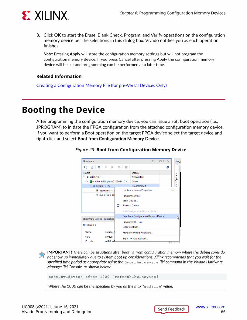
3. Click OK to start the Erase, Blank Check, Program, and Verify operations on the configurationmemory device per the selections in this dialog box. Vivado notifies you as each operationfinishes.
Note: Pressing Apply will store the configuration memory settings but will not program theconfiguration memory device. If you press Cancel after pressing Apply the configuration memorydevice will be set and programming can be performed at a later time.
Related Information
Creating a Configuration Memory File (for pre-Versal Devices Only)
Booting the DeviceAfter programming the configuration memory device, you can issue a soft boot operation (i.e.,JPROGRAM) to initiate the FPGA configuration from the attached configuration memory device.If you want to perform a Boot operation on the target FPGA device select the target device andright-click and select Boot from Configuration Memory Device.
Figure 23: Boot from Configuration Memory Device
IMPORTANT! There can be situations after booting from configuration memory where the debug cores donot show up immediately due to system boot up considerations. Xilinx recommends that you wait for thespecified time period as appropriate using the boot_hw_device Tcl command in the Vivado HardwareManager Tcl Console, as shown below:
boot_hw_device after 1000 [refresh_hw_device]
Where the 1000 can be the specified by you as the max "wait_on" value.
Chapter 6: Programming Configuration Memory Devices
UG908 (v2021.1) June 16, 2021 www.xilinx.comVivado Programming and Debugging 66Send Feedback
Configuration Failures in Master ModeNote: The following is not supported on MPSoC or Versal architectures.
Configuration failures can occur when a board is in Master BPI or Master SPI mode and the JTAGcable is connected to the Vivado Hardware Manager. When the Hardware Manager polling andrecover feature interrupts the Master mode configuration, intermittent configuration failuresoccur on power up. To avoid this issue, set the following parameter in the Vivado HardwareManager Tcl console to ensure that the configuration status registers are not updated:
set_param xicom.allow_cfgin_commands false
Note: This parameter affects all devices in the chain.
Chapter 6: Programming Configuration Memory Devices
UG908 (v2021.1) June 16, 2021 www.xilinx.comVivado Programming and Debugging 67Send Feedback

Chapter 7
Advanced Programming Features
Readback and Verify for 7 Series, UltraScale,and UltraScale+ FPGAs and MPSoCs
Bitstream Verify and ReadbackNote: The following is not applicable to Versal architectures.
Vivado® IDE can verify and/or readback the configuration data (i.e., .bit file) downloaded intoan FPGA. When using write_bitstream to generate the .bit file, use the -mask_fileoption to create a corresponding mask (.msk) file. Run write_bitstream-help in the VivadoIDE Tcl Console for details on bitstream generation options.
When performing a verify operation, the verify_hw_devices Tcl command reads data backfrom the FPGA and uses the .msk file to determine which readback data bits to skip and whichones to compare against the corresponding bits in the .bit file.
Following is an example of a bitstream verify Tcl command sequence (the .bit and .msk fileswere generated by a previous call to write_bitstream):
create_hw_bitstream -hw_device [current_hw_device] \ -mask kcu105_cnt_ila_uncmpr.msk kcu105_cnt_ila_uncmpr.bitverify_hw_devices [current_hw_device]
You can use the Vivado Hardware Manager to verify the configuration data. Right click thedevice, select Verify Device as shown below.
Chapter 7: Advanced Programming Features
UG908 (v2021.1) June 16, 2021 www.xilinx.comVivado Programming and Debugging 68Send Feedback
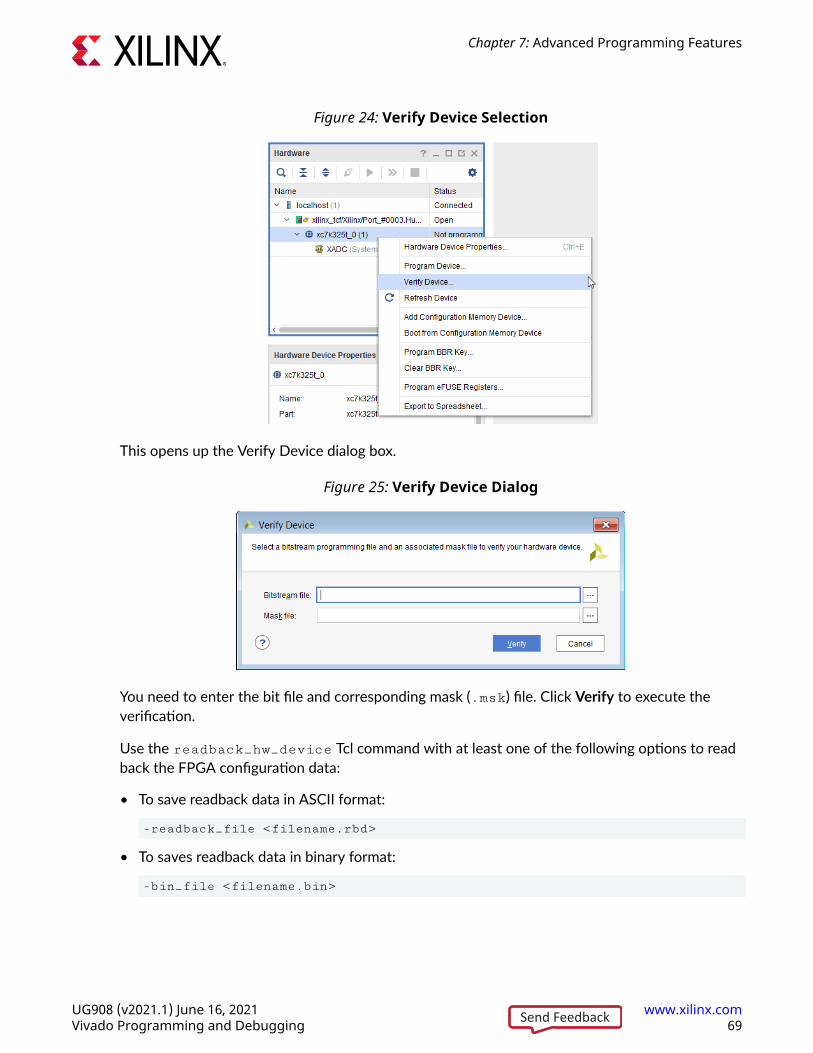
Figure 24: Verify Device Selection
This opens up the Verify Device dialog box.
Figure 25: Verify Device Dialog
You need to enter the bit file and corresponding mask (.msk) file. Click Verify to execute theverification.
Use the readback_hw_device Tcl command with at least one of the following options to readback the FPGA configuration data:
• To save readback data in ASCII format:
-readback_file <filename.rbd>
• To saves readback data in binary format:
-bin_file <filename.bin>
Chapter 7: Advanced Programming Features
UG908 (v2021.1) June 16, 2021 www.xilinx.comVivado Programming and Debugging 69Send Feedback
Example: Readback FPGA configuration data in both ASCII and binary formats:
readback_hw_device [current_hw_device] \ -readback_file kcu105_cnt_ila_uncmpr_rb.rbd \ -bin_file kcu105_cnt_ila_uncmpr_rb.bin
1. Bitstream, and readback operations are done through the Tcl Console.
2. Verify and readback operations do not work for FPGAs programmed with encryptedbitstreams. Encrypted bitstreams contain commands that disable readback. Readback is re-enabled by pulsing the FPGA PROG pin, or if the FPGA/board is powered down and poweredback up again.
3. The data readback using readback_hw_device contains configuration data only (noconfiguration commands are included).
For more information on the readback and mask files, see the "Verifying Readback Data" sectionin the UltraScale Architecture Configuration User Guide (UG570) or the 7 Series FPGAs ConfigurationUser Guide (UG470).
Configuration Memory Verify and ReadbackYou can convert a bitstream file (.bit) to an .mcs or .bin file and then program it into aconfiguration memory device, such as serial/SPI or parallel/BPI flash, via the write_cfgmemcommand. See theVivado Design Suite Tcl Command Reference Guide (UG835) for details.
Verify the configuration memory device through the Vivado Design Suite Hardware Manager asshown in the following figure.
Chapter 7: Advanced Programming Features
UG908 (v2021.1) June 16, 2021 www.xilinx.comVivado Programming and Debugging 70Send Feedback
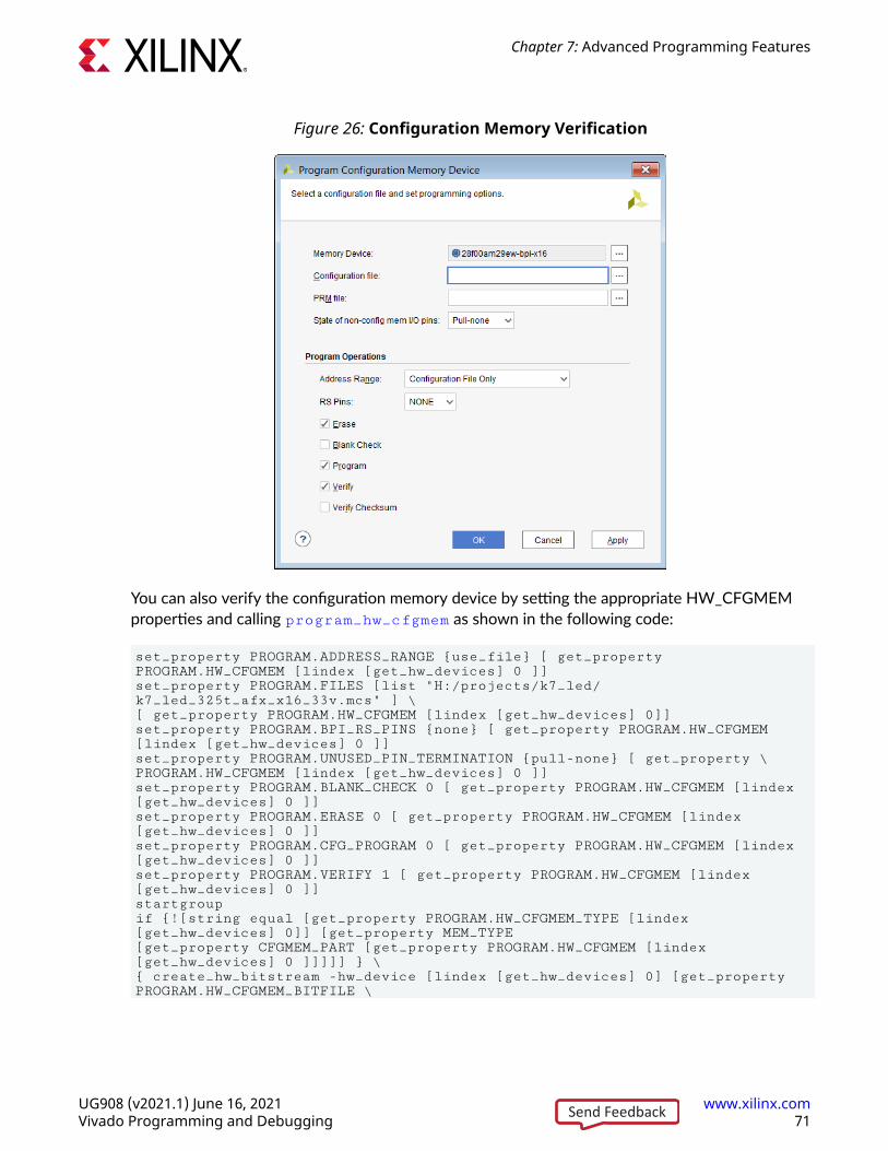
Figure 26: Configuration Memory Verification
You can also verify the configuration memory device by setting the appropriate HW_CFGMEMproperties and calling program_hw_cfgmem as shown in the following code:
set_property PROGRAM.ADDRESS_RANGE {use_file} [ get_property PROGRAM.HW_CFGMEM [lindex [get_hw_devices] 0 ]]set_property PROGRAM.FILES [list "H:/projects/k7_led/k7_led_325t_afx_x16_33v.mcs" ] \[ get_property PROGRAM.HW_CFGMEM [lindex [get_hw_devices] 0]]set_property PROGRAM.BPI_RS_PINS {none} [ get_property PROGRAM.HW_CFGMEM [lindex [get_hw_devices] 0 ]]set_property PROGRAM.UNUSED_PIN_TERMINATION {pull-none} [ get_property \PROGRAM.HW_CFGMEM [lindex [get_hw_devices] 0 ]]set_property PROGRAM.BLANK_CHECK 0 [ get_property PROGRAM.HW_CFGMEM [lindex [get_hw_devices] 0 ]]set_property PROGRAM.ERASE 0 [ get_property PROGRAM.HW_CFGMEM [lindex [get_hw_devices] 0 ]]set_property PROGRAM.CFG_PROGRAM 0 [ get_property PROGRAM.HW_CFGMEM [lindex [get_hw_devices] 0 ]]set_property PROGRAM.VERIFY 1 [ get_property PROGRAM.HW_CFGMEM [lindex [get_hw_devices] 0 ]]startgroupif {![string equal [get_property PROGRAM.HW_CFGMEM_TYPE [lindex [get_hw_devices] 0]] [get_property MEM_TYPE[get_property CFGMEM_PART [get_property PROGRAM.HW_CFGMEM [lindex [get_hw_devices] 0 ]]]]] } \{ create_hw_bitstream -hw_device [lindex [get_hw_devices] 0] [get_property PROGRAM.HW_CFGMEM_BITFILE \
Chapter 7: Advanced Programming Features
UG908 (v2021.1) June 16, 2021 www.xilinx.comVivado Programming and Debugging 71Send Feedback
[ lindex [get_hw_devices] 0]]; program_hw_devices [lindex [get_hw_devices] 0]; };program_hw_cfgmem -hw_cfgmem [get_property PROGRAM.HW_CFGMEM [lindex [get_hw_devices] 0 ]]endgroup
The contents of the configuration memory can be readback through the Vivado Design Suite TclConsole using the following command sequence:
readback_hw_cfgmem -file test.bin -hw_cfgmem \ [get_property PROGRAM.HW_CFGMEM [lindex [get_hw_devices] 0]]
Note: Perform configuration memory readback operations through the Tcl Console only.
For more information on these features, see the UltraScale Architecture Configuration User Guide(UG570) or the 7 Series FPGAs Configuration User Guide (UG470).
Generating Encrypted and Authenticated Filesfor 7 Series Devices
Note: For additional information please refer to Using Encryption to Secure a 7 Series FPGA Bitstream(XAPP1239).
To generate an encrypted bitstream, open an implemented design in Vivado IDE. From the maintoolbar Select Flow → Bitstream Settings to make the Settings dialog box appear. At the top ofthe dialog box click Configure Additional Bitstream Settings.
Chapter 7: Advanced Programming Features
UG908 (v2021.1) June 16, 2021 www.xilinx.comVivado Programming and Debugging 72Send Feedback
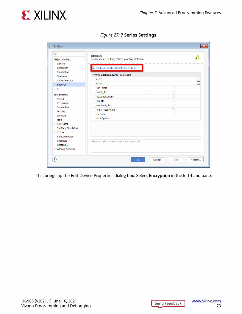
Figure 27: 7 Series Settings
This brings up the Edit Device Properties dialog box. Select Encryption in the left-hand pane.
Chapter 7: Advanced Programming Features
UG908 (v2021.1) June 16, 2021 www.xilinx.comVivado Programming and Debugging 73Send Feedback
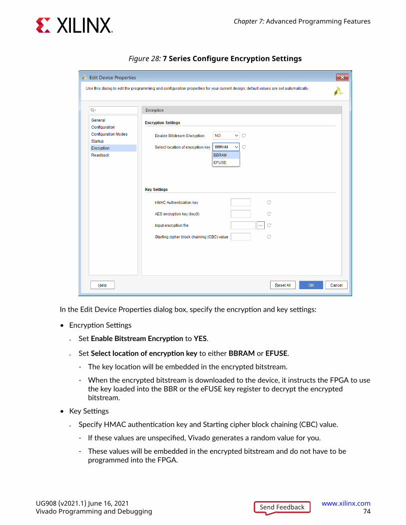
Figure 28: 7 Series Configure Encryption Settings
In the Edit Device Properties dialog box, specify the encryption and key settings:
• Encryption Settings
○ Set Enable Bitstream Encryption to YES.
○ Set Select location of encryption key to either BBRAM or EFUSE.
- The key location will be embedded in the encrypted bitstream.
- When the encrypted bitstream is downloaded to the device, it instructs the FPGA to usethe key loaded into the BBR or the eFUSE key register to decrypt the encryptedbitstream.
• Key Settings
○ Specify HMAC authentication key and Starting cipher block chaining (CBC) value.
- If these values are unspecified, Vivado generates a random value for you.
- These values will be embedded in the encrypted bitstream and do not have to beprogrammed into the FPGA.
Chapter 7: Advanced Programming Features
UG908 (v2021.1) June 16, 2021 www.xilinx.comVivado Programming and Debugging 74Send Feedback
Note: These values will be stored in the current project constraints file unless an input encryption fileis specified. To avoid storing this value in the constraints file, specify the input encryption file.
○ Specify the AES encryption key to use when encrypting the bitstream. You can use up to64 hex characters to specify the 256-bit key.
- The key will be written to a file with the .nky file extension. Use this file when loadingthe key into the BBR or when programming the key into the eFUSE key register.
Note: These values will be stored in the current project constraints file unless an input encryption fileis specified. To avoid storing this value in the constraints file, specify the input encryption file.
○ Specify Input encryption file.
- Specify an existing .nky file to obtain the encryption key settings. This field is optionaland can be omitted if specifying the AES, HMAC and CBC manually.
After specifying the encryption settings, click OK to apply the settings to the project andregenerate your bitstream. Upon successful completion of the write_bitstream operationyou will have a programming file along with a .nky, encryption file.
Generating Encrypted and Authenticated Filesfor UltraScale and UltraScale+
Note: For additional information refer to Using Encryption and Authentication to Secure an UltraScale/UltraScale+ FPGA Bitstream (XAPP1267).
To generate an encrypted bitstream, open an implemented design in Vivado IDE. From the maintoolbar select Flow → Bitstream Settings to make the Settings dialog box appear. At the top ofthe dialog box, click Configure Additional Bitstream Settings.
Chapter 7: Advanced Programming Features
UG908 (v2021.1) June 16, 2021 www.xilinx.comVivado Programming and Debugging 75Send Feedback
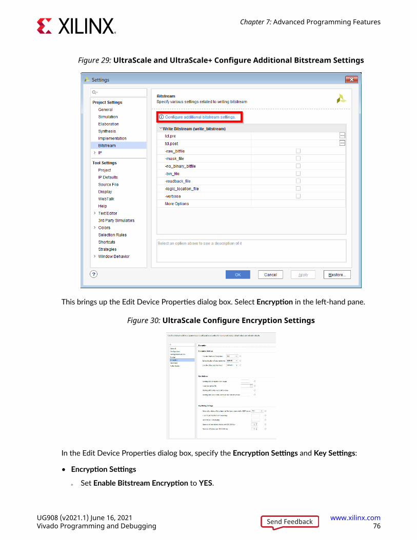
Figure 29: UltraScale and UltraScale+ Configure Additional Bitstream Settings
This brings up the Edit Device Properties dialog box. Select Encryption in the left-hand pane.
Figure 30: UltraScale Configure Encryption Settings
In the Edit Device Properties dialog box, specify the Encryption Settings and Key Settings:
• Encryption Settings
○ Set Enable Bitstream Encryption to YES.
Chapter 7: Advanced Programming Features
UG908 (v2021.1) June 16, 2021 www.xilinx.comVivado Programming and Debugging 76Send Feedback
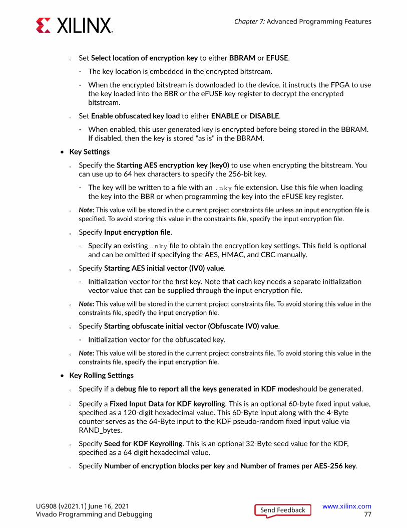
○ Set Select location of encryption key to either BBRAM or EFUSE.
- The key location is embedded in the encrypted bitstream.
- When the encrypted bitstream is downloaded to the device, it instructs the FPGA to usethe key loaded into the BBR or the eFUSE key register to decrypt the encryptedbitstream.
○ Set Enable obfuscated key load to either ENABLE or DISABLE.
- When enabled, this user generated key is encrypted before being stored in the BBRAM.If disabled, then the key is stored "as is" in the BBRAM.
• Key Settings
○ Specify the Starting AES encryption key (key0) to use when encrypting the bitstream. Youcan use up to 64 hex characters to specify the 256-bit key.
- The key will be written to a file with an .nky file extension. Use this file when loadingthe key into the BBR or when programming the key into the eFUSE key register.
○ Note: This value will be stored in the current project constraints file unless an input encryption file isspecified. To avoid storing this value in the constraints file, specify the input encryption file.
○ Specify Input encryption file.
- Specify an existing .nky file to obtain the encryption key settings. This field is optionaland can be omitted if specifying the AES, HMAC, and CBC manually.
○ Specify Starting AES initial vector (IV0) value.
- Initialization vector for the first key. Note that each key needs a separate initializationvector value that can be supplied through the input encryption file.
○ Note: This value will be stored in the current project constraints file. To avoid storing this value in theconstraints file, specify the input encryption file.
○ Specify Starting obfuscate initial vector (Obfuscate IV0) value.
- Initialization vector for the obfuscated key.
○ Note: This value will be stored in the current project constraints file. To avoid storing this value in theconstraints file, specify the input encryption file.
• Key Rolling Settings
○ Specify if a debug file to report all the keys generated in KDF modeshould be generated.
○ Specify a Fixed Input Data for KDF keyrolling. This is an optional 60-byte fixed input value,specified as a 120-digit hexadecimal value. This 60-Byte input along with the 4-Bytecounter serves as the 64-Byte input to the KDF pseudo-random fixed input value viaRAND_bytes.
○ Specify Seed for KDF Keyrolling. This is an optional 32-Byte seed value for the KDF,specified as a 64 digit hexadecimal value.
○ Specify Number of encryption blocks per key and Number of frames per AES-256 key.
Chapter 7: Advanced Programming Features
UG908 (v2021.1) June 16, 2021 www.xilinx.comVivado Programming and Debugging 77Send Feedback
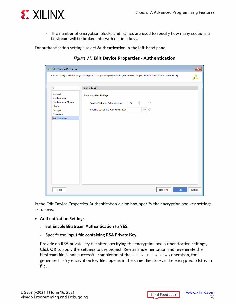
- The number of encryption blocks and frames are used to specify how many sections abitstream will be broken into with distinct keys.
For authentication settings select Authentication in the left-hand pane
Figure 31: Edit Device Properties - Authentication
In the Edit Device Properties-Authentication dialog box, specify the encryption and key settingsas follows:
• Authentication Settings
○ Set Enable Bitstream Authentication to YES.
○ Specify the Input file containing RSA Private Key.
Provide an RSA private key file after specifying the encryption and authentication settings,Click OK to apply the settings to the project. Re-run Implementation and regenerate thebitstream file. Upon successful completion of the write_bitstream operation, thegenerated .nky encryption key file appears in the same directory as the encrypted bitstreamfile.
Chapter 7: Advanced Programming Features
UG908 (v2021.1) June 16, 2021 www.xilinx.comVivado Programming and Debugging 78Send Feedback
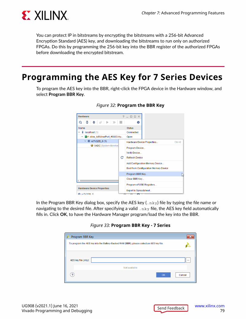
You can protect IP in bitstreams by encrypting the bitstreams with a 256-bit AdvancedEncryption Standard (AES) key, and downloading the bitstreams to run only on authorizedFPGAs. Do this by programming the 256-bit key into the BBR register of the authorized FPGAsbefore downloading the encrypted bitstream.
Programming the AES Key for 7 Series DevicesTo program the AES key into the BBR, right-click the FPGA device in the Hardware window, andselect Program BBR Key.
Figure 32: Program the BBR Key
In the Program BBR Key dialog box, specify the AES key (.nky) file by typing the file name ornavigating to the desired file. After specifying a valid .nky file, the AES key field automaticallyfills in. Click OK, to have the Hardware Manager program/load the key into the BBR.
Figure 33: Program BBR Key - 7 Series
Chapter 7: Advanced Programming Features
UG908 (v2021.1) June 16, 2021 www.xilinx.comVivado Programming and Debugging 79Send Feedback
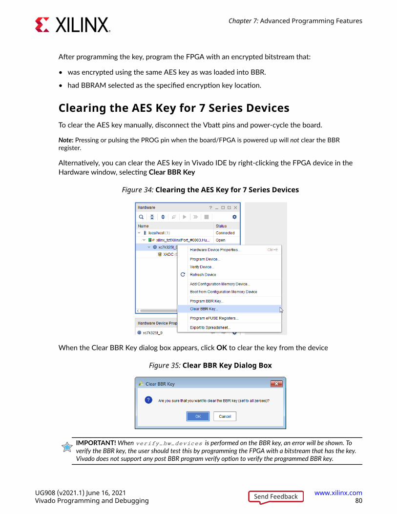
After programming the key, program the FPGA with an encrypted bitstream that:
• was encrypted using the same AES key as was loaded into BBR.
• had BBRAM selected as the specified encryption key location.
Clearing the AES Key for 7 Series DevicesTo clear the AES key manually, disconnect the Vbatt pins and power-cycle the board.
Note: Pressing or pulsing the PROG pin when the board/FPGA is powered up will not clear the BBRregister.
Alternatively, you can clear the AES key in Vivado IDE by right-clicking the FPGA device in theHardware window, selecting Clear BBR Key
Figure 34: Clearing the AES Key for 7 Series Devices
When the Clear BBR Key dialog box appears, click OK to clear the key from the device
Figure 35: Clear BBR Key Dialog Box
IMPORTANT! When verify_hw_devices is performed on the BBR key, an error will be shown. Toverify the BBR key, the user should test this by programming the FPGA with a bitstream that has the key.Vivado does not support any post BBR program verify option to verify the programmed BBR key.
Chapter 7: Advanced Programming Features
UG908 (v2021.1) June 16, 2021 www.xilinx.comVivado Programming and Debugging 80Send Feedback
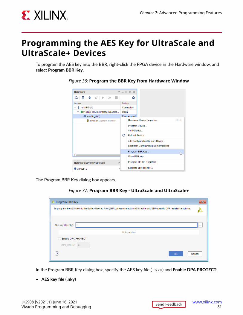
Programming the AES Key for UltraScale andUltraScale+ Devices
To program the AES key into the BBR, right-click the FPGA device in the Hardware window, andselect Program BBR Key.
Figure 36: Program the BBR Key from Hardware Window
The Program BBR Key dialog box appears.
Figure 37: Program BBR Key - UltraScale and UltraScale+
In the Program BBR Key dialog box, specify the AES key file (.nky) and Enable DPA PROTECT:
• AES key file (.nky)
Chapter 7: Advanced Programming Features
UG908 (v2021.1) June 16, 2021 www.xilinx.comVivado Programming and Debugging 81Send Feedback
○ Specify the AES key file (.nky) by typing the file name or navigating to the desired file. Afterspecifying a valid .nky file, the AES key field automatically fills in.
• Enable DPA PROTECT
○ Check the Enable DPA PROTECT check box.
○ Specify the DPA_COUNT value. The valid range is 1-256 when enabled.
Note: For more details on the BBR AES key and DPA_PROTECT feature refer to the UltraScaleArchitecture Configuration User Guide (UG570).
Click OK, to have the Hardware Manager program load the key into the BBR.
After programming the key, program the FPGA with an encrypted bitstream that:
• was encrypted using the same AES key as was loaded into BBR.
• had BBRAM selected as the specified encryption key location.
IMPORTANT! For UltraScale devices, if you download an encrypted bitstream (which uses the BBR asthe key source) before programming the key into the BBR register, the FPGA device will lock up and youwill not be able to load the BBR key. You can still download unencrypted bitstreams, but you will not beable to download encrypted bitstreams because the FPGA device will prevent you from downloading akey into BBR. You must power-cycle the board to unlock the UltraScale device and then reload the BBRkey.
IMPORTANT! When verify_hw_devices is performed on the BBR key, an error will be shown. Toverify the BBR key, the user should test this by programming the FPGA with a bitstream that has thekey. Vivado does not support any post BBR program verify option to verify the programmed BBR key.
Clearing the AES Key for UltraScale, and UltraScale+DevicesTo clear the AES key manually, disconnect the Vbatt pins and power-cycle the board.
Note: Pressing or pulsing the PROG pin when the board/FPGA is powered up will not clear the BBRregister.
Alternatively, you can clear the AES key in Vivado IDE by right-clicking the FPGA device in theHardware window, selecting Clear BBR Key
Chapter 7: Advanced Programming Features
UG908 (v2021.1) June 16, 2021 www.xilinx.comVivado Programming and Debugging 82Send Feedback
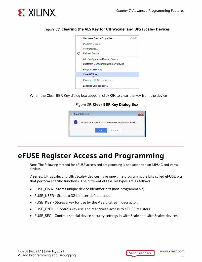
Figure 38: Clearing the AES Key for UltraScale, and UltraScale+ Devices
When the Clear BBR Key dialog box appears, click OK to clear the key from the device
Figure 39: Clear BBR Key Dialog Box
eFUSE Register Access and ProgrammingNote: The following method for eFUSE access and programming is not supported on MPSoC and Versaldevices.
7 series, UltraScale, and UltraScale+ devices have one-time programmable bits called eFUSE bitsthat perform specific functions. The different eFUSE bit types are as follows:
• FUSE_DNA - Stores unique device identifier bits (non-programmable).
• FUSE_USER - Stores a 32-bit user-defined code.
• FUSE_KEY - Stores a key for use by the AES bitstream decryptor.
• FUSE_CNTL - Controls key use and read/write access to eFUSE registers.
• FUSE_SEC - Controls special device security settings in UltraScale and UltraScale+ devices.
Chapter 7: Advanced Programming Features
UG908 (v2021.1) June 16, 2021 www.xilinx.comVivado Programming and Debugging 83Send Feedback

IMPORTANT! Programming eFUSE register bits is a one-time only operation. Once eFUSE register bitsare programmed (i.e., from unprogrammed state 0 to programmed 1 state), they cannot be reset to 0and/or programmed again. You should take great care to double-check your settings beforeprogramming any eFUSE registers.
CAUTION! If any eFUSE register bits have been previously programmed (i.e., from unprogrammedstate 0 to programmed state 1) and an attempt is made to program them again, the Vivado hardwaremanager issues a critical warning indicating that some bits have already been programmed. However,despite this warning, subsequent eFUSE register bits that have not been programmed during theprevious operation (in unprogrammed state 0) will be programmed.
IMPORTANT! Xilinx recommends programming the FUSE_USER, FUSE_KEY, and FUSE_RSA registersfirst, then rerunning the eFUSE programming wizard to program the FUSE_SEC bits to control the FPGAsecurity settings, and then finally, the FUSE_CNTL bits to control read/write access to these eFUSE bits.
Cable Support for eFUSE ProgrammingThe list of compatible JTAG download cables and devices that support efuse programming are:
• Xilinx® SmartLynq Data Cable (HW-SMARTLYNQ-G/DLC20)
• Xilinx Platform Cable USB II (DLC10)
• Digilent JTAG-HS1
• Digilent JTAG-HS2
• Digilent JTAG-HS3
eFUSE Register Access and Programming for 7Series Devices
FUSE_DNA: Unique Device DNAEach 7 series device has a unique device ID called device DNA that has already beenprogrammed into it by Xilinx. 7 series devices have a 64-bit DNA. You can read these bits byrunning the following Tcl command in the Vivado Design Suite Tcl Console:
get_property [lindex [get_hw_device] 0] REGISTER.EFUSE.FUSE_DNA
You can also access the device DNA by viewing the eFUSE registers in the Hardware DeviceProperties window in Vivado Design Suite as shown in the following figure.
Chapter 7: Advanced Programming Features
UG908 (v2021.1) June 16, 2021 www.xilinx.comVivado Programming and Debugging 84Send Feedback
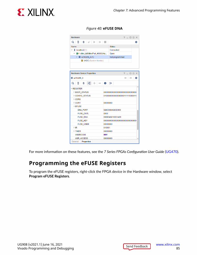
Figure 40: eFUSE DNA
For more information on these features, see the 7 Series FPGAs Configuration User Guide (UG470).
Programming the eFUSE RegistersTo program the eFUSE registers, right-click the FPGA device in the Hardware window, selectProgram eFUSE Registers.
Chapter 7: Advanced Programming Features
UG908 (v2021.1) June 16, 2021 www.xilinx.comVivado Programming and Debugging 85Send Feedback
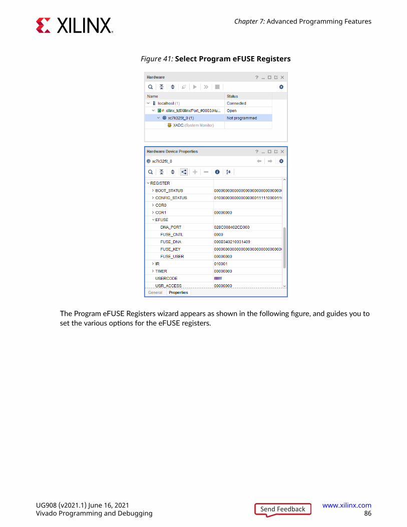
Figure 41: Select Program eFUSE Registers
The Program eFUSE Registers wizard appears as shown in the following figure, and guides you toset the various options for the eFUSE registers.
Chapter 7: Advanced Programming Features
UG908 (v2021.1) June 16, 2021 www.xilinx.comVivado Programming and Debugging 86Send Feedback
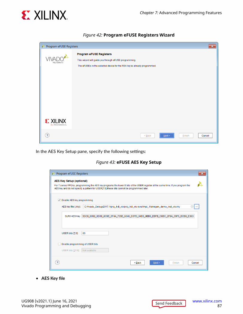
Figure 42: Program eFUSE Registers Wizard
In the AES Key Setup pane, specify the following settings:
Figure 43: eFUSE AES Key Setup
• AES Key file
Chapter 7: Advanced Programming Features
UG908 (v2021.1) June 16, 2021 www.xilinx.comVivado Programming and Debugging 87Send Feedback
○ Specify the AES key file (.nky) by typing the file name or navigating to the desired file.After specifying a valid .nky file, the AES key field automatically fills in.
• USER bits [7:0] and USER bits [31:8]
○ The USER eFUSEs bits are provided to allow users to program their own special 32-bitpattern. The lower eight FUSE_USER bits are programmed at the same time as the 256-bitAdvanced Encryption Engine (AES) key. The upper 24 user bits can be programmedconcurrently with AES key or at a later time
In the Control Register Settings pane, specify the following settings:
Figure 44: Control Register Setup
• CFG_AES_Only: When set, forces the use of the stored AES key.
• AES_Exclusive: When set, disables use of partial reconfiguration.
• W_EN_B_Key_User: When set, disables programing of AES key and User register.
• R_EN_B_Key: When set, disables reading of AES key.
• R_EN_B_User: When set, disables reading of user code.
• W_EN_B_Cntl: When set, disables programing of this control register.
For more information on these features, see the 7 Series FPGAs Configuration User Guide (UG470).
Review the eFUSE settings in the Program eFUSE Registers Summary page.
Chapter 7: Advanced Programming Features
UG908 (v2021.1) June 16, 2021 www.xilinx.comVivado Programming and Debugging 88Send Feedback
Figure 45: Program eFUSE Registers Summary
All bits set in the Program eFUSE Registers wizard panels are shown in this pane. In this pane youwill see individual bit settings in order to review the specific programming settings. Review thissummary page carefully to ensure every bit that is intended to be programmed is set.
Click Finish to bring up the Program eFUSE confirmation dialog box:
Figure 46: Program eFUSE Confirmation
Click OK the to program the specified fuse bits.
Forcing eFUSE ProgrammingTo force any bit to be set regardless of where it is in the register or whether it has beenpreviously programmed the -force_efuse option to program_hw_devices can be used.When used, only basic register boundary checking will occur.
Chapter 7: Advanced Programming Features
UG908 (v2021.1) June 16, 2021 www.xilinx.comVivado Programming and Debugging 89Send Feedback
eFUSE Register Access and Programming forUltraScale and UltraScale+ Devices
FUSE_DNA: Unique Device DNAEach UltraScale device has a unique device ID called device DNA that has already beenprogrammed into it by Xilinx. The FUSE_DNA is not user programmable. UltraScale devices havea 96-bit DNA. You can read the FUSE_DNA by running the following Tcl command in the VivadoDesign Suite Tcl Console:
get_property [lindex [get_hw_device] 0] REGISTER.EFUSE.FUSE_DNA
You can also access the device DNA by viewing the eFUSE registers in the Hardware DeviceProperties window in Vivado Design Suite as shown in the following figure.
Figure 47: eFUSE DNA UltraScale, UltraScale+
Chapter 7: Advanced Programming Features
UG908 (v2021.1) June 16, 2021 www.xilinx.comVivado Programming and Debugging 90Send Feedback
For more information on these features, see the UltraScale Architecture Configuration User Guide(UG570).
Programming the eFUSE RegistersTo program the eFUSE registers, right-click the FPGA device in the Hardware window, selectProgram eFUSE Registers.
Figure 48: Select Program eFUSE Registers UltraScale, UltraScale+
The Program eFUSE Registers wizard appears as shown in the following figure, and guides you toset the various options for the eFUSE registers.
Chapter 7: Advanced Programming Features
UG908 (v2021.1) June 16, 2021 www.xilinx.comVivado Programming and Debugging 91Send Feedback
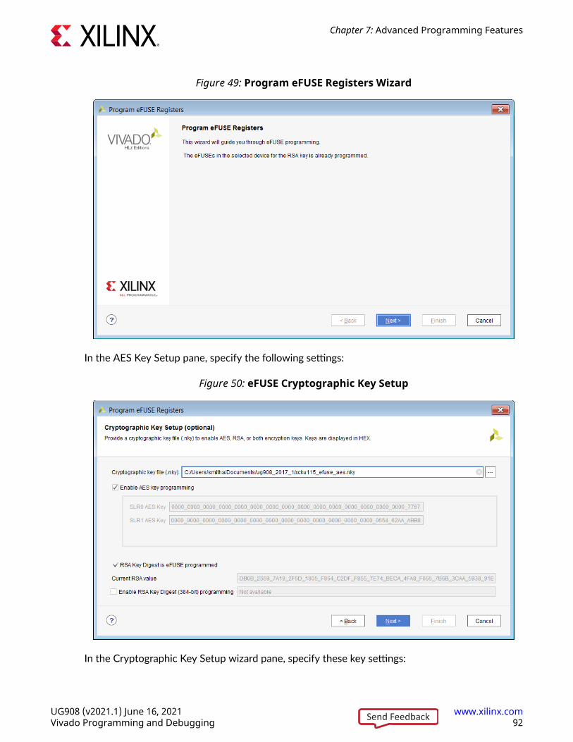
Figure 49: Program eFUSE Registers Wizard
In the AES Key Setup pane, specify the following settings:
Figure 50: eFUSE Cryptographic Key Setup
In the Cryptographic Key Setup wizard pane, specify these key settings:
Chapter 7: Advanced Programming Features
UG908 (v2021.1) June 16, 2021 www.xilinx.comVivado Programming and Debugging 92Send Feedback
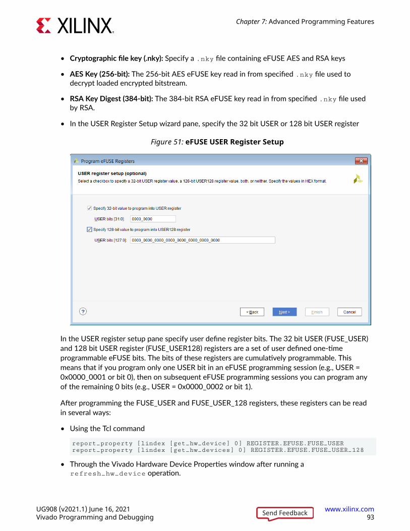
• Cryptographic file key (.nky): Specify a .nky file containing eFUSE AES and RSA keys
• AES Key (256-bit): The 256-bit AES eFUSE key read in from specified .nky file used todecrypt loaded encrypted bitstream.
• RSA Key Digest (384-bit): The 384-bit RSA eFUSE key read in from specified .nky file usedby RSA.
• In the USER Register Setup wizard pane, specify the 32 bit USER or 128 bit USER register
Figure 51: eFUSE USER Register Setup
In the USER register setup pane specify user define register bits. The 32 bit USER (FUSE_USER)and 128 bit USER register (FUSE_USER128) registers are a set of user defined one-timeprogrammable eFUSE bits. The bits of these registers are cumulatively programmable. Thismeans that if you program only one USER bit in an eFUSE programming session (e.g., USER =0x0000_0001 or bit 0), then on subsequent eFUSE programming sessions you can program anyof the remaining 0 bits (e.g., USER = 0x0000_0002 or bit 1).
After programming the FUSE_USER and FUSE_USER_128 registers, these registers can be readin several ways:
• Using the Tcl command
report_property [lindex [get_hw_device] 0] REGISTER.EFUSE.FUSE_USERreport_property [lindex [get_hw_devices] 0] REGISTER.EFUSE.FUSE_USER_128
• Through the Vivado Hardware Device Properties window after running arefresh_hw_device operation.
Chapter 7: Advanced Programming Features
UG908 (v2021.1) June 16, 2021 www.xilinx.comVivado Programming and Debugging 93Send Feedback
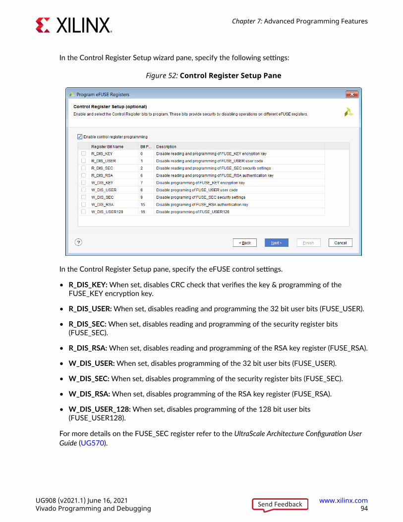
In the Control Register Setup wizard pane, specify the following settings:
Figure 52: Control Register Setup Pane
In the Control Register Setup pane, specify the eFUSE control settings.
• R_DIS_KEY: When set, disables CRC check that verifies the key & programming of theFUSE_KEY encryption key.
• R_DIS_USER: When set, disables reading and programming the 32 bit user bits (FUSE_USER).
• R_DIS_SEC: When set, disables reading and programming of the security register bits(FUSE_SEC).
• R_DIS_RSA: When set, disables reading and programming of the RSA key register (FUSE_RSA).
• W_DIS_USER: When set, disables programming of the 32 bit user bits (FUSE_USER).
• W_DIS_SEC: When set, disables programming of the security register bits (FUSE_SEC).
• W_DIS_RSA: When set, disables programming of the RSA key register (FUSE_RSA).
• W_DIS_USER_128: When set, disables programming of the 128 bit user bits(FUSE_USER128).
For more details on the FUSE_SEC register refer to the UltraScale Architecture Configuration UserGuide (UG570).
Chapter 7: Advanced Programming Features
UG908 (v2021.1) June 16, 2021 www.xilinx.comVivado Programming and Debugging 94Send Feedback
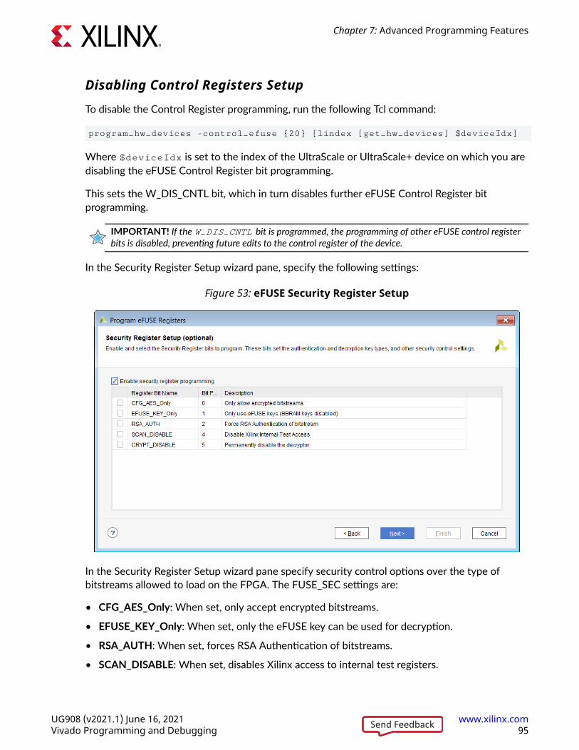
Disabling Control Registers Setup
To disable the Control Register programming, run the following Tcl command:
program_hw_devices -control_efuse {20} [lindex [get_hw_devices] $deviceIdx]
Where $deviceIdx is set to the index of the UltraScale or UltraScale+ device on which you aredisabling the eFUSE Control Register bit programming.
This sets the W_DIS_CNTL bit, which in turn disables further eFUSE Control Register bitprogramming.
IMPORTANT! If the W_DIS_CNTL bit is programmed, the programming of other eFUSE control registerbits is disabled, preventing future edits to the control register of the device.
In the Security Register Setup wizard pane, specify the following settings:
Figure 53: eFUSE Security Register Setup
In the Security Register Setup wizard pane specify security control options over the type ofbitstreams allowed to load on the FPGA. The FUSE_SEC settings are:
• CFG_AES_Only: When set, only accept encrypted bitstreams.
• EFUSE_KEY_Only: When set, only the eFUSE key can be used for decryption.
• RSA_AUTH: When set, forces RSA Authentication of bitstreams.
• SCAN_DISABLE: When set, disables Xilinx access to internal test registers.
Chapter 7: Advanced Programming Features
UG908 (v2021.1) June 16, 2021 www.xilinx.comVivado Programming and Debugging 95Send Feedback
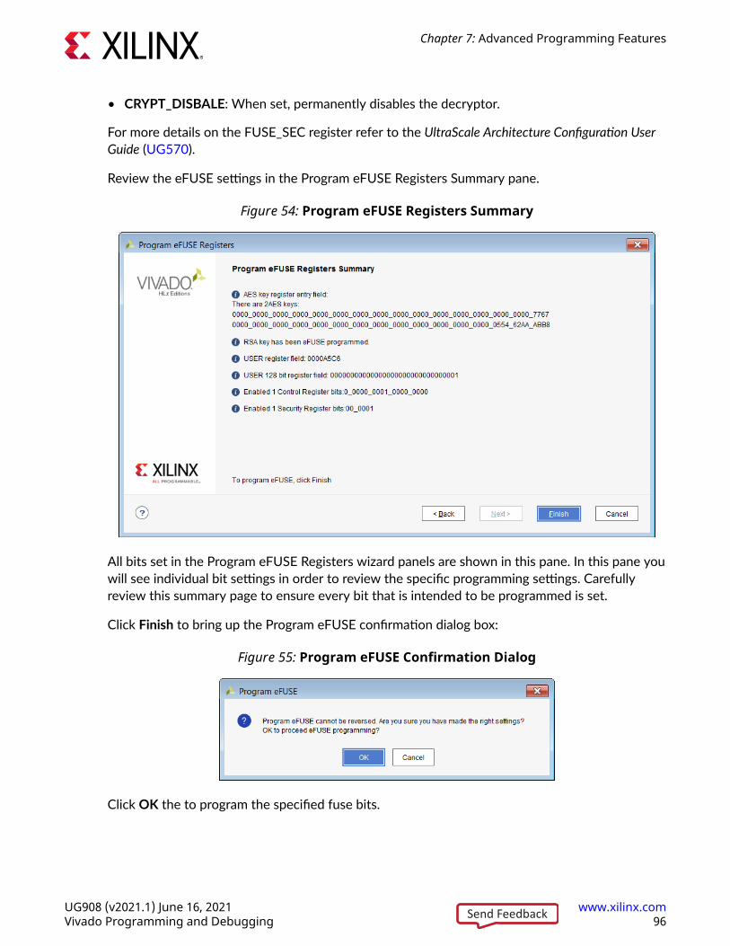
• CRYPT_DISBALE: When set, permanently disables the decryptor.
For more details on the FUSE_SEC register refer to the UltraScale Architecture Configuration UserGuide (UG570).
Review the eFUSE settings in the Program eFUSE Registers Summary pane.
Figure 54: Program eFUSE Registers Summary
All bits set in the Program eFUSE Registers wizard panels are shown in this pane. In this pane youwill see individual bit settings in order to review the specific programming settings. Carefullyreview this summary page to ensure every bit that is intended to be programmed is set.
Click Finish to bring up the Program eFUSE confirmation dialog box:
Figure 55: Program eFUSE Confirmation Dialog
Click OK the to program the specified fuse bits.
Chapter 7: Advanced Programming Features
UG908 (v2021.1) June 16, 2021 www.xilinx.comVivado Programming and Debugging 96Send Feedback
Disabling the JTAG interfaceTo disable the JTAG interface through the eFUSE registers, run the following Tcl command:
program_hw_devices -force_efuse -security_efuse {08} [lindex [get_hw_devices] $deviceIdx]
Where $deviceIdx is set to the index of the UltraScale or UltraScale+ device that will have itsJTAG interface disabled.
IMPORTANT! The Tcl command to disable the JTAG interface for 7 series differs from command usedabove for UltraScale or UltraScale+ devices. If a 7 series device is used, see the entry forXSK_EFUSEPL_DISABLE_JTAG_CHAIN listed in Xilinx Answer Record 65110.
Note: This programming step should be performed as the last and final step after all desired eFUSE bitshave been programmed.
IMPORTANT! If the JTAG Disable bit is programmed, the JTAG interface will be disabled, preventingfuture test and configuration access to the device. This bit should only be programmed if JTAG access tothe device is no longer required.
Forcing eFUSE ProgrammingTo force any bit to be set regardless of where it is in the register or whether it has beenpreviously programmed the -force_efuse option to program_hw_devices can be used.When used, only basic register boundary checking will occur.
eFUSE NKZ FileIn order to capture all eFUSE programming settings in one file, and so make it easier to exporteFUSE settings to other eFUSE programmer implementations, as well as to mass-program thesame eFUSE settings into many devices, Xilinx has defined a file format called NKZ, designatedby the file extension .nkz. The NKZ format is a superset of the existing NKY format; that is,NKZ supports all NKY fields as well as any programmable eFUSE register settings.
eFUSE Export NKZ FileBecause you are advised to program eFUSE settings in multiple passes, eFUSE settings arealways exported to an externally visible NKZ file which is updated during each eFUSE operation.The intent of this file is to accumulate all eFUSE settings applied to a device, even if they areapplied over multiple eFUSE operations. This file is tracked by Vivado so that there is always asingle eFUSE export file containing the cumulative eFUSE settings for a device in NKZ format.
Chapter 7: Advanced Programming Features
UG908 (v2021.1) June 16, 2021 www.xilinx.comVivado Programming and Debugging 97Send Feedback
If no options are specified, the default name of this file is as follows, where <FUSE_DNA> is theFUSE_DNA register value of the device.
export_<FUSE_DNA>.nkz
This default file is located in the launch directory of the Vivado IDE. You can change this file byusing the -efuse_export_file option on the program_hw_devices Tcl command, as inthe following example:
program_hw_devices -user_efuse {1} -efuse_export_file {my_settings.nkz}
The Vivado IDE then starts using the specified NKZ file for exported eFUSE settings withouthaving to repeatedly specify this file in the Tcl options. Any previously created eFUSE export filewill not be removed; it will contain all the eFUSE settings applied prior to changing the eFUSEexport file name. After all eFUSE operations are performed, all eFUSE settings are stored in thecurrent eFUSE export file.
There is also an option to only export eFUSE settings instead of actually programming the device.This can be useful for creating an NKZ file containing all the desired eFUSE settings withoutaffecting the device. Any eFUSE programming mistakes made in this mode can easily becorrected by removing the eFUSE export file and starting over. This export-only mode can beused with the following Tcl command:
program_hw_devices -user_efuse {1} -only_export_efuse
This option applies only to each individual command, so the option must be used in every eFUSEoperation to keep the device from being programmed. Because eFUSE settings are alwaysexported to an NKZ file regardless of whether or not programming occurs, it is recommended notto intermix the programming flow with the export-only flow. Otherwise, the resulting eFUSEexport file might contain a mix of eFUSE settings actually programmed into the device and thoseonly exported to the NKZ file, which makes the true state of the eFUSE registers in the deviceunclear. Using this export-only mode, the same exact eFUSE export file in NKZ format is createdas in the programming case, but no programming is performed on the device.
It is also possible to skip programming the encryption keys that are specified in the NKZ file byusing the -skip_program_keys option on the program-hw_devices Tcl command.
• For 7 series devices, if -skip_program_keys is specified, the programming of FUSE_AES isskipped, no check to validate AES keys in the encryption file is performed, and theprogramming continues.
• For 7 series devices, -skip_program_keys must not be used if the NKZ also contains anon-zero FUSE_USER setting because FUSE_AES and FUSE_USER values must beprogrammed together in the 7 series device.
• For UltraScale and UltraScale+ devices, the setting of FUSE_SEC[6] is skipped if -skip_program_keys is used when programming obfuscated keys.
Chapter 7: Advanced Programming Features
UG908 (v2021.1) June 16, 2021 www.xilinx.comVivado Programming and Debugging 98Send Feedback
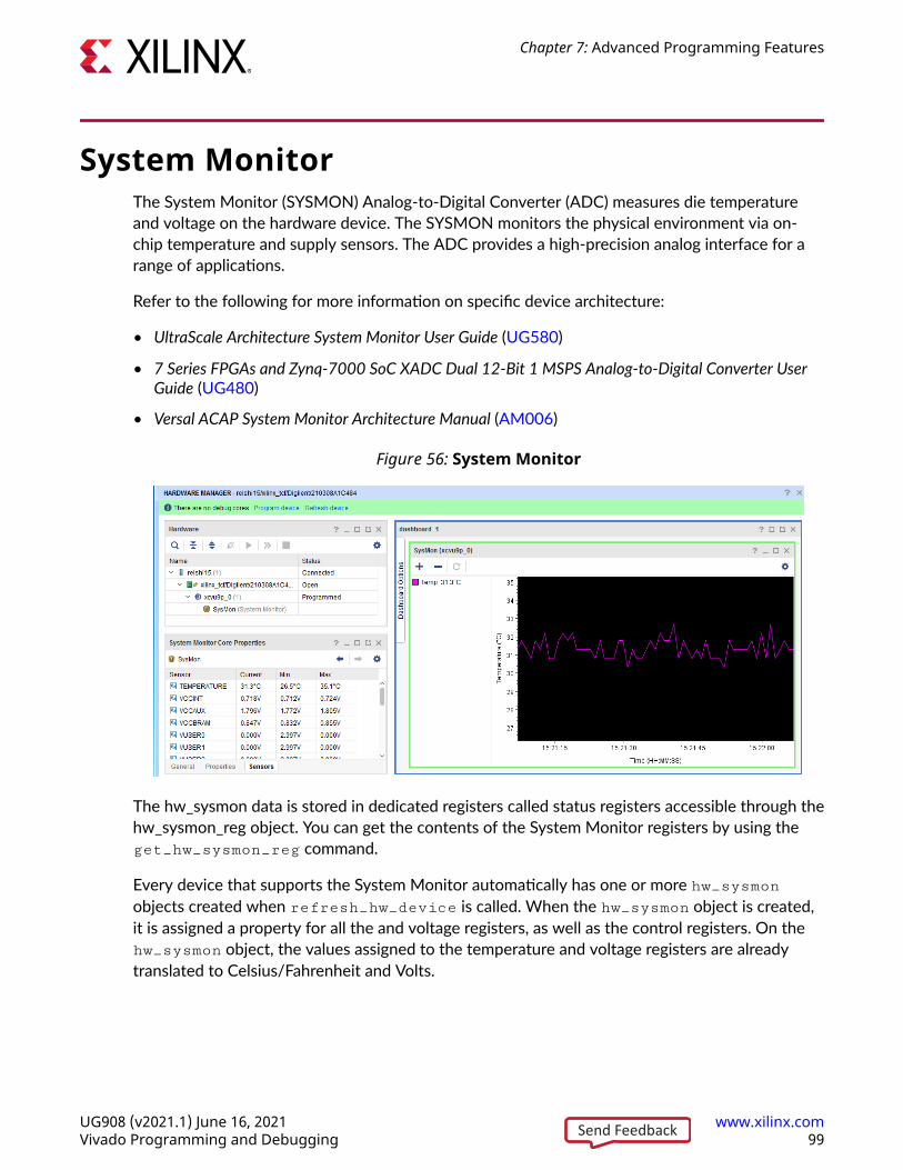
System MonitorThe System Monitor (SYSMON) Analog-to-Digital Converter (ADC) measures die temperatureand voltage on the hardware device. The SYSMON monitors the physical environment via on-chip temperature and supply sensors. The ADC provides a high-precision analog interface for arange of applications.
Refer to the following for more information on specific device architecture:
• UltraScale Architecture System Monitor User Guide (UG580)
• 7 Series FPGAs and Zynq-7000 SoC XADC Dual 12-Bit 1 MSPS Analog-to-Digital Converter UserGuide (UG480)
• Versal ACAP System Monitor Architecture Manual (AM006)
Figure 56: System Monitor
The hw_sysmon data is stored in dedicated registers called status registers accessible through thehw_sysmon_reg object. You can get the contents of the System Monitor registers by using theget_hw_sysmon_reg command.
Every device that supports the System Monitor automatically has one or more hw_sysmonobjects created when refresh_hw_device is called. When the hw_sysmon object is created,it is assigned a property for all the and voltage registers, as well as the control registers. On thehw_sysmon object, the values assigned to the temperature and voltage registers are alreadytranslated to Celsius/Fahrenheit and Volts.
Chapter 7: Advanced Programming Features
UG908 (v2021.1) June 16, 2021 www.xilinx.comVivado Programming and Debugging 99Send Feedback
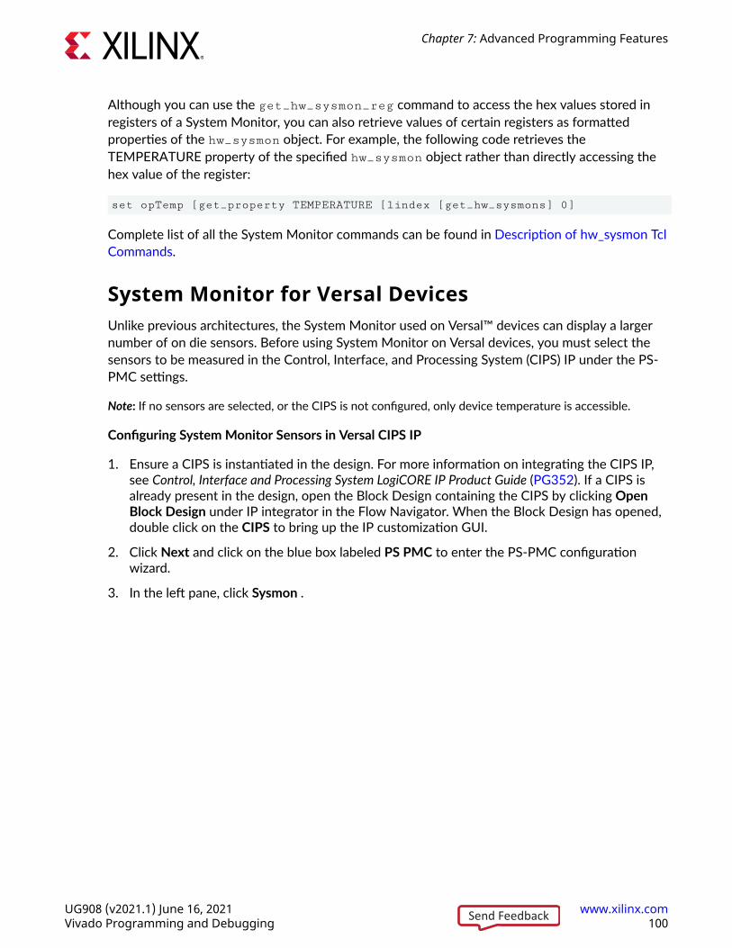
Although you can use the get_hw_sysmon_reg command to access the hex values stored inregisters of a System Monitor, you can also retrieve values of certain registers as formattedproperties of the hw_sysmon object. For example, the following code retrieves theTEMPERATURE property of the specified hw_sysmon object rather than directly accessing thehex value of the register:
set opTemp [get_property TEMPERATURE [lindex [get_hw_sysmons] 0]
Complete list of all the System Monitor commands can be found in Description of hw_sysmon TclCommands.
System Monitor for Versal DevicesUnlike previous architectures, the System Monitor used on Versal™ devices can display a largernumber of on die sensors. Before using System Monitor on Versal devices, you must select thesensors to be measured in the Control, Interface, and Processing System (CIPS) IP under the PS-PMC settings.
Note: If no sensors are selected, or the CIPS is not configured, only device temperature is accessible.
Configuring System Monitor Sensors in Versal CIPS IP
1. Ensure a CIPS is instantiated in the design. For more information on integrating the CIPS IP,see Control, Interface and Processing System LogiCORE IP Product Guide (PG352). If a CIPS isalready present in the design, open the Block Design containing the CIPS by clicking OpenBlock Design under IP integrator in the Flow Navigator. When the Block Design has opened,double click on the CIPS to bring up the IP customization GUI.
2. Click Next and click on the blue box labeled PS PMC to enter the PS-PMC configurationwizard.
3. In the left pane, click Sysmon .
Chapter 7: Advanced Programming Features
UG908 (v2021.1) June 16, 2021 www.xilinx.comVivado Programming and Debugging 100Send Feedback
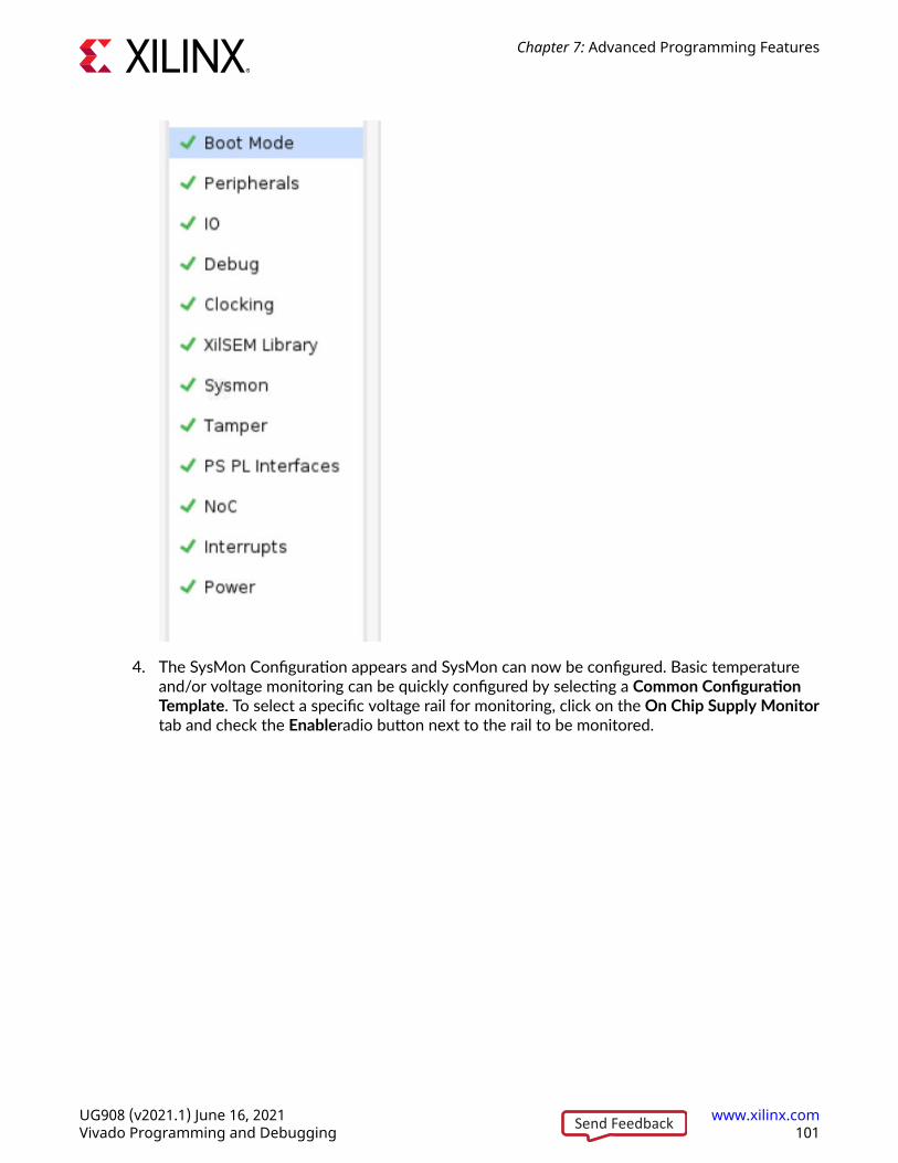
4. The SysMon Configuration appears and SysMon can now be configured. Basic temperatureand/or voltage monitoring can be quickly configured by selecting a Common ConfigurationTemplate. To select a specific voltage rail for monitoring, click on the On Chip Supply Monitortab and check the Enableradio button next to the rail to be monitored.
Chapter 7: Advanced Programming Features
UG908 (v2021.1) June 16, 2021 www.xilinx.comVivado Programming and Debugging 101Send Feedback
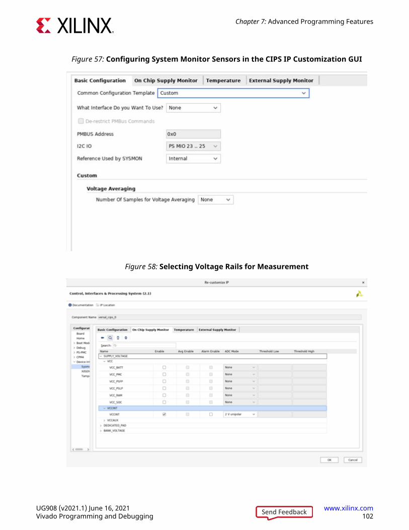
Figure 57: Configuring System Monitor Sensors in the CIPS IP Customization GUI
Figure 58: Selecting Voltage Rails for Measurement
Chapter 7: Advanced Programming Features
UG908 (v2021.1) June 16, 2021 www.xilinx.comVivado Programming and Debugging 102Send Feedback
Chapter 8
Serial Vector Format (SVF) FileProgramming
Note: Serial Vector Format (SVF) programming is not supported on Versal™ devices.
An alternative way to program FPGAs and configuration memory devices is through the use of aserial vector format (SVF) file. The SVF file generated through Vivado® Design Suite and VivadoLab Edition contains low level JTAG instructions and data required to program these devices.Once the file is generated it can be used by boundary scan test tools independent of the VivadoIDE.
The general steps to create an SVF file are as follows:
1. Create an SVF offline target.
2. Open the created SVF target.
3. Add devices to the target to define the SVF JTAG scan chain.
4. Program FPGAs or configuration memory devices.
5. Write SVF.
6. Close SVF target.
7. (Optional) Execute SVF.
In step 4, the program operations are recorded in sequential order and stored a cached file. Thecached file is then written out to a target destination in step 5. After the file is created, it can beused by boundary scan tools or executed through Vivado Design Suite or Vivado Lab Editiontools.
IMPORTANT! The XSVF file format is not supported in Vivado IDE.
Chapter 8: Serial Vector Format (SVF) File Programming
UG908 (v2021.1) June 16, 2021 www.xilinx.comVivado Programming and Debugging 103Send Feedback
Creating an SVF TargetThe SVF target is similar to a live Xilinx Platform Cable USB or Digilent JTAG cable hardwaretarget. The properties and Tcl commands are all the same with the main distinction being that theSVF target is not an active live cable. This means that any operations performed on this targetwill not affect the hardware until the SVF is executed. Note that you do not need to have a cableconnected to your system to create an SVF.
Using Vivado IDETo create an SVF target in the Vivado Hardware Manager, open the Vivado Hardware Managerby either launching Vivado or Vivado Lab Edition. You can create an SVF Target by selectingTools → Create SVF Target. This automatically opens a server on the local host, and also opensthe Create SVF Target dialog as box shown in the following figure.
On any available server you can create an offline SVF target as shown below.
Figure 59: Create SVF Target
The Create SVF Target dialog box opens as shown below.
Chapter 8: Serial Vector Format (SVF) File Programming
UG908 (v2021.1) June 16, 2021 www.xilinx.comVivado Programming and Debugging 104Send Feedback
Figure 60: Create SVF Target Dialog Box
TIP: You can copy an existing SVF chain by enabling the Copy from target option. Alternatively you canspecify an SVF file that you created using the Vivado Hardware Manager from an earlier run of the flow.Vivado IDE saves specifics of the SVF chain, so when it is read back, the SVF chain can be recreated.
The SVF Target that you just created appears Open under the your server in the Hardwarewindow in Vivado Hardware Manager.
Figure 61: SVF Target in Hardware Window
To delete an existing SVF target, right-click the SVF target in the Hardware window and selectDelete.
Chapter 8: Serial Vector Format (SVF) File Programming
UG908 (v2021.1) June 16, 2021 www.xilinx.comVivado Programming and Debugging 105Send Feedback
Figure 62: Delete SVF Target in Hardware Window
IMPORTANT! When you delete a target, all the devices created for that target are also deleted. Moreover,a deleted target is also closed if it was previously opened.
You can also use the Vivado Tcl mode or the Tcl Console in the Vivado IDE to create the SVFTarget.
Following are the steps needed to create an SVF target after initially launching Vivado or VivadoLab Edition:
Using the Command LineFollowing are the steps needed to create an SVF target after initially launching Vivado or VivadoLab Edition:
open_hw_managerconnect_hw_servercreate_hw_target my_svf_targetif {[string length [get_hw_targets -quiet -filter{IS_OPENED == TRUE}]] > 0} \{close_hw_target [get_hw_targets * -filter {IS_OPENED == TRUE}] }; \open_hw_target [get_hw_targets *my_svf_target]current_hw_target
The first two commands can be omitted if already connected to a server. When executed, thecreate_hw_target command defines the my_svf_target. Note that you cannot have twotargets with the same name in a session. Finally, after closing any open target and opening thesvf target, the create_hw_target command is run. As a result, the final command shows the fullhardware target handle name of the created my_svf_target.
Chapter 8: Serial Vector Format (SVF) File Programming
UG908 (v2021.1) June 16, 2021 www.xilinx.comVivado Programming and Debugging 106Send Feedback
All standard operations on the target, such as get_hw_targets and open_hw_targetcommandsare supported. You can use the IS_SVF hardware target property to distinguishbetween a live target and an SVF target. For instance, the following is a sample command linethat reads the IS_SVF property from a target named "my_svf_target".
get_property IS_SVF [get_hw_targets -regexp .*my_svf_target]
Additionally, all the SVF hw_targets created in this session can be displayed by issuing thefollowing command:
get_hw_targets -filter {IS_SVF}
To delete the created target, use the delete_hw_target command. For instance, by issuingthe following command, the my_svf_target is deleted:
delete_hw_target [get_hw_targets -regexp .*my_svf_target]
IMPORTANT! When a target is deleted, all the devices created for the target are also deleted. Moreover adeleted target is also closed if it was previously opened.
Adding Devices to an SVF TargetAfter the SVF target is created, devices can be added to it in order to define the SVF JTAG devicechain configuration. The SVF JTAG device chain configuration should match the target hardwarechain to ensure proper SVF file execution.
Using Vivado IDEClick the + button to add Xilinx or non-Xilinx parts to the SVF chain.
Figure 63: Add Devices to SVF Target
When you click Add Xilinx Part, the Add Xilinx Device dialog box opens. You can now choose theappropriate Xilinx device to append to the SVF chain.
Chapter 8: Serial Vector Format (SVF) File Programming
UG908 (v2021.1) June 16, 2021 www.xilinx.comVivado Programming and Debugging 107Send Feedback
Note: Devices can only be appended to an SVF device chain.
Figure 64: Add Xilinx Device Dialog Box
TIP: This dialog box is slightly different in Vivado ML Enterprise.
On selecting a Xilinx Device and clicking OK, the Xilinx Device is added to the SVF chain asshown in the following figure.
Figure 65: Xilinx Device in SVF Chain
You can also add non-Xilinx parts to the SVF device chain by right-clicking the SVF chain andselecting Add Non-Xilinx Part as shown below.
Chapter 8: Serial Vector Format (SVF) File Programming
UG908 (v2021.1) June 16, 2021 www.xilinx.comVivado Programming and Debugging 108Send Feedback
Figure 66: Adding a Non-Xilinx Part
This opens the Add Non-Xilinx Device dialog box as shown below.
Figure 67: Add Non-Xilinx Device Dialog Box
Fill in the dialog box as follows:
• The Part Name can be any part name you choose.
• The ID Code is a Hex value that represents a valid device ID code.
• The IR length is a decimal numerical value that represents the Instruction Register length.
• The Mask is a Hex bit mask value.
Note: The ID code, IR Length, and Mask values are typically provided by silicon vendors through deviceBSDL files.
Click OK, and the Non-Xilinx part is added to the SVF Device chain.
Chapter 8: Serial Vector Format (SVF) File Programming
UG908 (v2021.1) June 16, 2021 www.xilinx.comVivado Programming and Debugging 109Send Feedback
Figure 68: Non-Xilinx Device in SVF Chain
Using the Command LineTo create the chain using the Vivado Tcl mode or the Tcl Console in the Vivado IDE, performsequential create_hw_device operations on an open SVF target. For instance, to add anxcku9p part followed by an xcvu095 part perform the following steps:
current_hw_target my_svf_targetopen_hw_targetcreate_hw_device -part xcku9p create_hw_device -part xcvu095 refresh_hw_targetget_hw_devices
In this example, the first two steps can be skipped if the SVF is already created and opened. Thecreate_hw_device commands in the example define the devices of the JTAG chain startingwith the first device on the chain and onward.
Note: The create_hw_device command only creates devices on an open SVF hardware target.
To add user defined devices to the chain, add the -idcode, -irlength, and -mask valuesalong with the part type name using the -part options. For instance, if you have a part called"my_part" with a JTAG idcode of 1234567, an ir length of 8, mask of ffffffff, then you wouldcreate the device as shown below:
open_hw_target [current_hw_target]create_hw_device -idcode 01234567 -irlength 8 -mask ffffffff -part my_part# print IR length for user defined devicesputs [get_property IR_LENGTH [lindex [get_hw_devices -filter {PART == my_part}] 0]]puts $idcode_hexclose_hw_target
Note: The idcode for the create_hw_device should be a valid device ID code. ID code values and IRlengths are typically provided by silicon vendors through device BSDL files.
Chapter 8: Serial Vector Format (SVF) File Programming
UG908 (v2021.1) June 16, 2021 www.xilinx.comVivado Programming and Debugging 110Send Feedback

To see a report of the target and its devices, run the report_hw_targets command. Thereport shows details for all active targets in the system. Use this report to obtain properties ofthe server, target, and device as shown below:
report_hw_targetsINFO: Server Property Information: localhost:3121 CLASS: hw_server HOST: localhost NAME: localhost:3121 PORT: 3121 SID: TCP:localhost:3121INFO: Target Property Information: localhost:3121/xilinx_tcf/Xilinx/my_svf_target CLASS: hw_target DEVICE_COUNT: 3 HW_JTAG: 0 IS_OPENED: 1 MAX_DEVICE_COUNT: 32 NAME: localhost:3121/xilinx_tcf/Xilinx/my_svf_target FREQUENCY: 10000000 TYPE: xilinx_tcf TID: jsn-XNC-my_svf_target UID: Xilinx/my_svf_target SVF: 1 Device: xcku9p_0 Device: xcvu095_1 Device: my_part_2
Adding Configuration Memory Parts to XilinxDevices
Using Vivado IDEWhen you right-click on a Xilinx device part in an SVF chain, you have the option of creating andassociating a Configuration Memory device to it.
Chapter 8: Serial Vector Format (SVF) File Programming
UG908 (v2021.1) June 16, 2021 www.xilinx.comVivado Programming and Debugging 111Send Feedback
Figure 69: Adding a Configuration Memory Device
This opens up the Add Configuration Memory Device dialog box as shown below.
Figure 70: Add Configuration Memory Device Dialog Box
Select the appropriate memory device and click OK. The device is associated with the Xilinxdevice and appears in the SVF device chain as shown below.
Chapter 8: Serial Vector Format (SVF) File Programming
UG908 (v2021.1) June 16, 2021 www.xilinx.comVivado Programming and Debugging 112Send Feedback
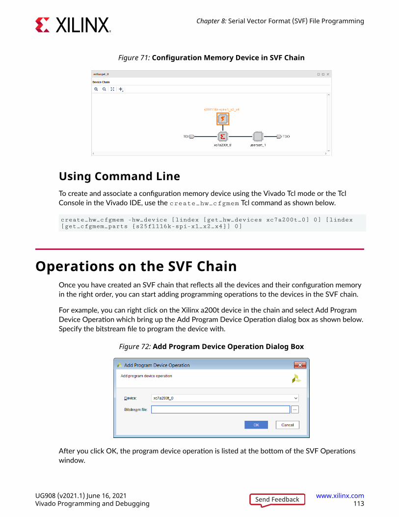
Figure 71: Configuration Memory Device in SVF Chain
Using Command LineTo create and associate a configuration memory device using the Vivado Tcl mode or the TclConsole in the Vivado IDE, use the create_hw_cfgmem Tcl command as shown below.
create_hw_cfgmem -hw_device [lindex [get_hw_devices xc7a200t_0] 0] [lindex [get_cfgmem_parts {s25fl116k-spi-x1_x2_x4}] 0]
Operations on the SVF ChainOnce you have created an SVF chain that reflects all the devices and their configuration memoryin the right order, you can start adding programming operations to the devices in the SVF chain.
For example, you can right click on the Xilinx a200t device in the chain and select Add ProgramDevice Operation which bring up the Add Program Device Operation dialog box as shown below.Specify the bitstream file to program the device with.
Figure 72: Add Program Device Operation Dialog Box
After you click OK, the program device operation is listed at the bottom of the SVF Operationswindow.
Chapter 8: Serial Vector Format (SVF) File Programming
UG908 (v2021.1) June 16, 2021 www.xilinx.comVivado Programming and Debugging 113Send Feedback
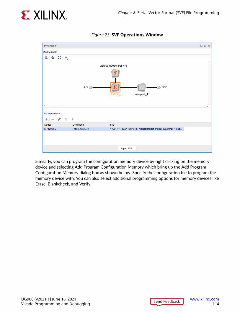
Figure 73: SVF Operations Window
Similarly, you can program the configuration memory device by right clicking on the memorydevice and selecting Add Program Configuration Memory which bring up the Add ProgramConfiguration Memory dialog box as shown below. Specify the configuration file to program thememory device with. You can also select additional programming options for memory devices likeErase, Blankcheck, and Verify.
Chapter 8: Serial Vector Format (SVF) File Programming
UG908 (v2021.1) June 16, 2021 www.xilinx.comVivado Programming and Debugging 114Send Feedback
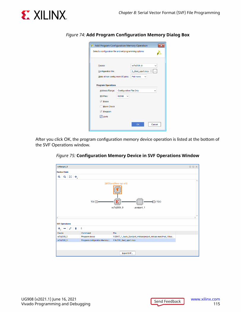
Figure 74: Add Program Configuration Memory Dialog Box
After you click OK, the program configuration memory device operation is listed at the bottom ofthe SVF Operations window.
Figure 75: Configuration Memory Device in SVF Operations Window
Chapter 8: Serial Vector Format (SVF) File Programming
UG908 (v2021.1) June 16, 2021 www.xilinx.comVivado Programming and Debugging 115Send Feedback
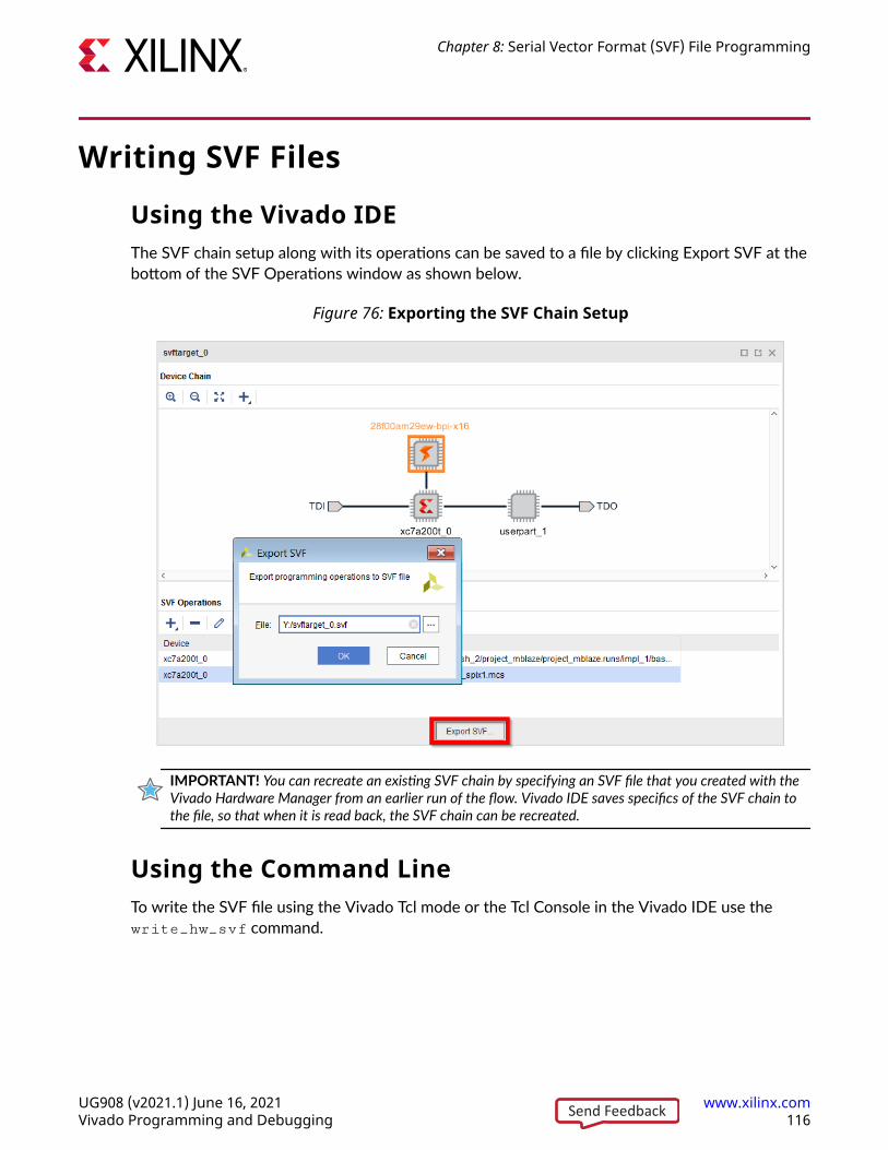
Writing SVF FilesUsing the Vivado IDEThe SVF chain setup along with its operations can be saved to a file by clicking Export SVF at thebottom of the SVF Operations window as shown below.
Figure 76: Exporting the SVF Chain Setup
IMPORTANT! You can recreate an existing SVF chain by specifying an SVF file that you created with theVivado Hardware Manager from an earlier run of the flow. Vivado IDE saves specifics of the SVF chain tothe file, so that when it is read back, the SVF chain can be recreated.
Using the Command LineTo write the SVF file using the Vivado Tcl mode or the Tcl Console in the Vivado IDE use thewrite_hw_svf command.
Chapter 8: Serial Vector Format (SVF) File Programming
UG908 (v2021.1) June 16, 2021 www.xilinx.comVivado Programming and Debugging 116Send Feedback
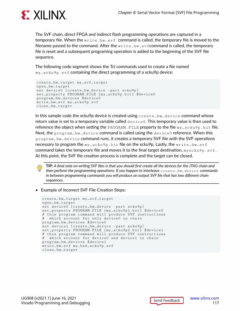
The SVF chain, direct FPGA and indirect flash programming operations are captured in atemporary file. When the write_hw_svf command is called, the temporary file is moved to thefilename passed to the command. After the write_hw_svfcommand is called, the temporaryfile is reset and a subsequent programing operation is added to the beginning of the SVF filesequence.
The following code segment shows the Tcl commands used to create a file namedmy_xcku9p.svf containing the direct programming of a xcku9p device:
create_hw_target my_svf_targetopen_hw_targetset device0 [create_hw_device -part xcku9p]set_property PROGRAM.FILE {my_xcku9p.bit} $device0program_hw_devices $device0write_hw_svf my_xcku9p.svfclose_hw_target
In this sample code the xcku9p device is created using create_hw_device command whosereturn value is set to a temporary variable called device0. This temporary value is then used toreference the object when setting the PROGRAM.FILE property to the file my_xcku9p.bit file.Next, the program_hw_device command is called using the device0 reference. When thisprogram_hw_device command runs, it creates a temporary SVF file with the SVF operationsnecessary to program the my_xcku9p.bit file on the xcku9p. Lastly, the write_hw_svfcommand takes the temporary file and moves it to the final target destination, myxcku9p.svf.At this point, the SVF file creation process is complete and the target can be closed.
TIP: A final note on writing SVF files is that you should first create all the devices for the JTAG chain andthen perform the programming operations. If you happen to interleave create_hw_device commandsin between programming commands you will produce an output SVF file that has two different chainsequences.
• Example of Incorrect SVF File Creation Steps:
create_hw_target my_svf_targetopen_hw_targetset device0 [create_hw_device -part xcku9p]set_property PROGRAM.FILE {my_xcku9p1.bit} $device0# this program command will produce SVF instructions # which account for only device0 in chainprogram_hw_devices $device0set device1 [create_hw_device -part xcku9p]set_property PROGRAM.FILE {my_xcku9p2.bit} $device1# this program command will produce SVF instructions # which account for device0 and device1 in chainprogram_hw_devices $device1write_hw_svf my_bad_xcku9p.svfclose_hw_target
Chapter 8: Serial Vector Format (SVF) File Programming
UG908 (v2021.1) June 16, 2021 www.xilinx.comVivado Programming and Debugging 117Send Feedback
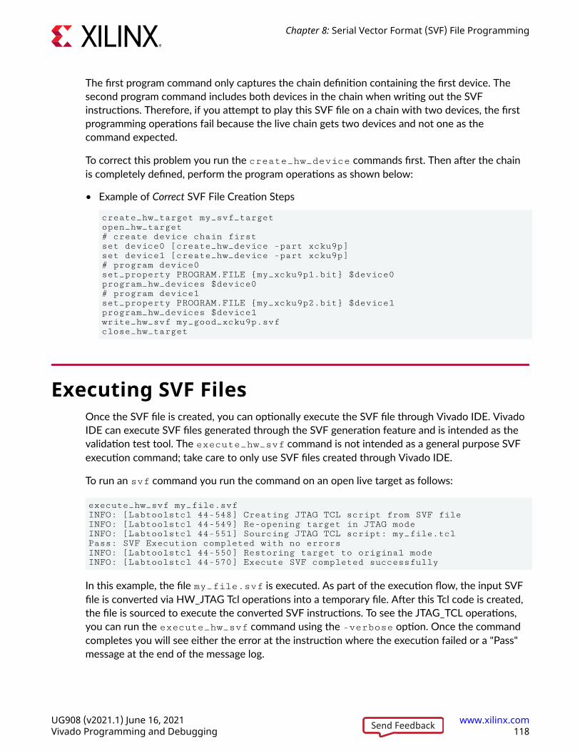
The first program command only captures the chain definition containing the first device. Thesecond program command includes both devices in the chain when writing out the SVFinstructions. Therefore, if you attempt to play this SVF file on a chain with two devices, the firstprogramming operations fail because the live chain gets two devices and not one as thecommand expected.
To correct this problem you run the create_hw_device commands first. Then after the chainis completely defined, perform the program operations as shown below:
• Example of Correct SVF File Creation Steps
create_hw_target my_svf_targetopen_hw_target# create device chain firstset device0 [create_hw_device -part xcku9p]set device1 [create_hw_device -part xcku9p]# program device0set_property PROGRAM.FILE {my_xcku9p1.bit} $device0program_hw_devices $device0# program device1set_property PROGRAM.FILE {my_xcku9p2.bit} $device1program_hw_devices $device1write_hw_svf my_good_xcku9p.svfclose_hw_target
Executing SVF FilesOnce the SVF file is created, you can optionally execute the SVF file through Vivado IDE. VivadoIDE can execute SVF files generated through the SVF generation feature and is intended as thevalidation test tool. The execute_hw_svf command is not intended as a general purpose SVFexecution command; take care to only use SVF files created through Vivado IDE.
To run an svf command you run the command on an open live target as follows:
execute_hw_svf my_file.svfINFO: [Labtoolstcl 44-548] Creating JTAG TCL script from SVF fileINFO: [Labtoolstcl 44-549] Re-opening target in JTAG modeINFO: [Labtoolstcl 44-551] Sourcing JTAG TCL script: my_file.tclPass: SVF Execution completed with no errorsINFO: [Labtoolstcl 44-550] Restoring target to original modeINFO: [Labtoolstcl 44-570] Execute SVF completed successfully
In this example, the file my_file.svf is executed. As part of the execution flow, the input SVFfile is converted via HW_JTAG Tcl operations into a temporary file. After this Tcl code is created,the file is sourced to execute the converted SVF instructions. To see the JTAG_TCL operations,you can run the execute_hw_svf command using the -verbose option. Once the commandcompletes you will see either the error at the instruction where the execution failed or a "Pass"message at the end of the message log.
Chapter 8: Serial Vector Format (SVF) File Programming
UG908 (v2021.1) June 16, 2021 www.xilinx.comVivado Programming and Debugging 118Send Feedback
Chapter 9
Debugging the DesignDebugging an FPGA or ACAP design is a multi-step, iterative process. Like most complexproblems, it is best to break the FPGA or ACAP design debugging process down into smallerparts by focusing on getting smaller sections of the design working one at a time rather thantrying to get the whole design to work at once. Iterating through the design flow by adding onemodule at a time and getting it to function properly in the context of the whole design is oneexample of a proven design and debug methodology. You can use this design and debugmethodology in any combination of the following design flow stages:
• RTL-level design simulation
• Post-implemented design simulation
• In-system debugging
RTL-Level Design SimulationThe design can be functionally debugged during the simulation verification process. Xilinxprovides a full design simulation feature in the Vivado® IDE. The Vivado design simulator can beused to perform RTL simulation of your design. The benefits of debugging your design in an RTL-level simulation environment include full visibility of the entire design and ability to quicklyiterate through the design/debug cycle. The limitations of debugging your design using RTL-levelsimulation includes the difficulty of simulating larger designs in a reasonable amount of time inaddition to the difficulty of accurately simulating the actual system environment. For moreinformation about using the Vivado simulator, refer to the Vivado Design Suite User Guide: LogicSimulation (UG900).
Post-Implemented Design SimulationThe Vivado simulator can also be used to simulate the post-implemented design. One of thebenefits of debugging the post-implemented design using the Vivado simulator includes havingaccess to a timing-accurate model for the design. The limitations of performing post-implemented design simulation include those mentioned in the previous section: long run-timesand system model accuracy.
Chapter 9: Debugging the Design
UG908 (v2021.1) June 16, 2021 www.xilinx.comVivado Programming and Debugging 119Send Feedback
In-System Logic Design DebuggingThe Vivado Design Suite also includes a logic analysis feature that enables you to perform in-system debugging of the post-implemented design in an FPGA or ACAP. The benefits fordebugging your design in-system include debugging your timing-accurate, post-implementeddesign in the actual system environment at system speeds. The limitations of in-systemdebugging includes somewhat lower visibility of debug signals compared to using simulationmodels and potentially longer design/implementation/debug iterations, depending on the sizeand complexity of the design.
In general, the Vivado tool provides several different ways to debug your design. You can use oneor more of these methods to debug your design, depending on your needs. In-System LogicDesign Debugging Flows focuses on the in-system logic debugging capabilities of the VivadoDesign Suite.
Related Information
In-System Logic Design Debugging Flows
In-System Serial I/O Design DebuggingTo enable in-system serial I/O validation and debug, the Vivado Design Suite includes a serial I/Oanalysis feature. This allows you to measure and optimize your high-speed serial I/O links in yourFPGA-based system. The Vivado serial I/O analyzer features are designed to help you address arange of in-system debug and validation problems from simple clocking and connectivity issuesto complex margin analysis and channel optimization issues. The main benefit of using the Vivadoserial I/O analyzer over some other external instrumentation techniques is that you aremeasuring the quality of the signal after the receiver equalization has been applied to thereceived signal. This ensures that you are measuring at the optimal point in the TX-to-RX channelthereby ensuring real and accurate data.
The Vivado tool provides the means to generate the design used to exercise the gigabittransceiver endpoints as well as the run-time software to take measurements and help youoptimize your high-speed serial I/O channels. Serial I/O Hardware Debugging Flows guides youthrough the process of generating the IBERT design. Debugging the Serial I/O Design inHardware guides you through the use of the run time Vivado serial I/O analyzer feature.
Related Information
Serial I/O Hardware Debugging FlowsDebugging the Serial I/O Design in Hardware
Chapter 9: Debugging the Design
UG908 (v2021.1) June 16, 2021 www.xilinx.comVivado Programming and Debugging 120Send Feedback

Chapter 10
In-System Logic Design DebuggingFlows
The Vivado® tool provides many features to debug a design in-system in an actual hardwaredevice. The in-system debugging flow has three distinct phases:
1. Probing phase: Identifying what signals in your design you want to probe and how you wantto probe them.
2. Implementation phase: Implementing the design that includes the additional debug IP that isattached to the probed nets.
3. Analysis phase: Interacting with the debug IP contained in the design to debug and verifyfunctional issues.
This in-system debug flow is designed to work using the iterative design/debug flow described inthe previous section. If you choose to use the in-system debugging flow, it is advisable to get apart of your design working in hardware as early in the design cycle as possible. The rest of thischapter describes the three phases of the in-system debugging flow and how to use the Vivadologic debug feature to get your design working in hardware as quickly as possible.
Probing the Design for In-System DebuggingThe probing phase of the in-system debugging flow is split into two steps:
1. Identifying what signals or nets you want to probe
2. Deciding how you want to add debug cores to your design
In many cases, the decision you make on what signals to probe or how to probe them can affectone another. It helps to start by deciding if you want to manually add the debug IP componentinstances to your design source code (called the HDL instantiation probing flow) or if you wantthe Vivado tool to automatically insert the debug cores into your post-synthesis netlist (calledthe netlist insertion probing flow). The following table describes some of the advantages andtrade-offs of the different debugging approaches.
Chapter 10: In-System Logic Design Debugging Flows
UG908 (v2021.1) June 16, 2021 www.xilinx.comVivado Programming and Debugging 121Send Feedback
Table 4: Debugging Strategies
Debugging Goal Recommended Debug Programming FlowIdentify debug signals in the HDL sourcecode while retaining flexibility to enable/disable debugging later in the flow.
Use mark_debug property to tag signals for debugging in HDL.Use the Set up Debug wizard to guide you through the Netlist Insertionprobing flow.
Identify debug nets in synthesized designnetlist without having to modify the HDLsource code.
Use the Mark Debug right-click menu option to select nets for debugging inthe synthesized design netlist.Use the Set up Debug wizard to guide you through the Netlist Insertionprobing flow.
Automated debug probing flow using Tclcommands.
Use set_property Tcl command to set the mark_debug property on debugnets.Use Netlist Insertion probing flow Tcl commands to create debug cores andconnect to them to debug nets.
Explicitly attach signals in the HDL sourceto an ILA debug core instance.
Identify HDL signals for debugging.Use the HDL Instantiation probing flow to generate and instantiate anIntegrated Logic Analyzer (ILA) core and connect it to the debug signals in thedesign.
Versal In-System DebuggingWhile the Xilinx® Versal™ ACAP architecture differs from previous FPGA architectures, and usesdifferent debug IP and infrastructure to connect the debug cores the in-system, the debuggingflow is similar in many ways to previous FPGA architectures. There are a few differences to beaware of as detailed in this section.
Adding a Control, Interface, and Processing System(CIPS)1. If the design does not already contain a block design, click Create Block Design under the IP
integrator category in the Flow Navigator to create one.
2. Click + to add new IP to the IP integrator Canvas and type cips to search for the CIPS IP (asshown in the following figure). Once found, double click to add it to the IP integrator canvas.
3. Once added, a green bar displays near the top of the tool bar indicating that designerassistance is available. It is not necessary to run block automation unless there is a need toconfigure additional options.
Chapter 10: In-System Logic Design Debugging Flows
UG908 (v2021.1) June 16, 2021 www.xilinx.comVivado Programming and Debugging 122Send Feedback
4. Click the button to validate the block design, then click the button to save the block design.
5. Generate the HDL wrapper for the Block Design by returning to the Project Manager, rightclicking on the newly created block design and selecting Create HDL Wrapper.
6. Once created, ensure this block design is instantiated as part of the design.
7. Proceed with using either the Netlist Insertion Debug Probing Flow, HDL Instantiation DebugProbing Flow, or the IP integrator Debug Flow. If the design contains any debug cores, theAXI4 Debug Hub will be automatically added to the netlist during opt_design and thedebug cores will be connected automatically
Note: By default, this block design will not have any input or output ports unless additional IPs areadded requiring I/O.
Note: For most applications it is not necessary to manually connect instantiated debug cores to the AXI4Debug Hub. During opt_design an instance of the AXI4 Debug Hub and NoC will be inserted into thenetlist and the connections between the debug cores, debug hub, and CIPS core will be automaticallystitched.
Note: For more information on design creation, simulation, and debug using the CIPS core, see Control,Interface and Processing System LogiCORE IP Product Guide (PG352).
AXI4-Debug HubVersal devices use the AXI4-Debug Hub, which is similar to the debug hub used in previousarchitectures and provides connectivity between the Versal Control, Interface, and Processing(CIPS) IP and the debug cores in the design. Just as in previous architectures Vivado inserts thiscore automatically without user intervention. It is also possible to manually instantiate the AXI4-Debug Hub. Manual instantiation is only recommended if using DFX, or the design's addressingscheme that requires setting a manual address for the AXI4-Debug Hub.
Chapter 10: In-System Logic Design Debugging Flows
UG908 (v2021.1) June 16, 2021 www.xilinx.comVivado Programming and Debugging 123Send Feedback
AXI4-Stream ILAVersal devices use the AXI4-Stream ILA that includes both ILA and System-ILA functionality. TheAXI4-Stream ILA also provides two choices for trace memory: Block RAM (BRAM) and UltraRAM(URAM).
AXI4-Debug Hub ConnectivityTo use the Vivado® debug cores, the design must contain an AXI4 debug hub. The AXI4 debughub connects an AXI-MM interface of the CIPS with the AXI4-Stream interface. The interfaceconnects to Vivado debug cores, which includes the following types of cores:
• AXI4-Stream Integrated Logic Analyzer (AXIS-ILA)
• AXI4-Stream Virtual Input/Output (AXIS-VIO)
• PCI Express® Link Debugger
Table 5: AXI4 Debug Hub Auto-Insertion
AXI4-Debug Hub Connectivity Debug Flow
Automatic AXI4-Debug Hub post-synthesis netlist insertionand connection.
This method is recommended for most usecases as itprovides the most flexibility.
1. During opt_designthe Vivado debug flow will detect ifthe design contains any debug cores that require AXI4-Debug Hub connectivity. The Vivado debug flow willalso detect if the design contains an instance of theControl, Interface, and Processing (CIPS) IP.
2. The Vivado debug flow will insert an instance of theAXI4-Debug Hub into the synthesized netlist andautomatically connect it to the debug cores used in thedesign.
Note: This method can not be used on designs that utilizeDynamic Function eXchange (DFX).
Chapter 10: In-System Logic Design Debugging Flows
UG908 (v2021.1) June 16, 2021 www.xilinx.comVivado Programming and Debugging 124Send Feedback
Table 5: AXI4 Debug Hub Auto-Insertion (cont'd)
AXI4-Debug Hub Connectivity Debug Flow
Manual AXI4-Debug Hub instantiation, automatic post-synthesis netlist debug core connection.
This method should be used when it is desired to manuallyassign the address used by the AXI4-Debug Hub or whenDynamic Function eXchange (DFX) is used. In this case thedesign should have a manually instantiated AXI4-DebugHub with a connection to an AXI-MM master from theControl, Interface, and Processing (CIPS) IP.
1. During opt_designthe Vivado debug flow will detect ifthe design contains any debug cores that require AXI4-Debug Hub Connectivity. The Vivado debug flow willalso detect if the design contains an instance of theControl, Interface, and Processing (CIPS) IP.
2. The Vivado debug flow will locate the manually addedAXI4-Debug Hub. This instance of the AXI4-Debug Hubwill be replaced with an AXI4-Debug Hub configuredwith a suitable number of AXI4-Stream interfaces toconnect to each debug core used in the design.
Note: The AXI4-Debug Hub that is replaced by the Vivadodebug flow in the above steps will retain the user specifiedaddress and properties.
Manual AXI4-Debug Hub instantiation, manual debug coreconnection.
This method should be used when it is desired to manuallydefine all connectivity between the AXI4-Debug Hub, CIPS,and all debug cores in the design. This method can also beused when the design uses Dynamic Function eXchange(DFX).
1. When building the design, one or more instances of theAXI4-Debug Hub are added to the design withconnectivity to an appropriate AXI-MM master on theCIPS IP.
2. The AXI4-Debug Hub should be customized to includethe exactnumber of AXI4-Stream interfaces as thereare debug cores in the design.
3. Each debug core in the design should have the optionto enable AXI4-Stream ports for manual connectivityturned on.
4. It is the user's responsibility to connect each debugcore's AXI4-Stream master and slave to acorresponding slave and master on the AXI4-DebugHub.
Manually Connecting Versal Debug CoresThe Versal AXI4-Debug Hub IP and debug cores (such as AXI4-Stream ILA, AXI4-Stream VIO)offer the option to manually define the connectivity between the debug cores and the AXI4-Debug Hub. This option is not required for most designs.
To enable manual connectivity to between the AXI4-Debug Hub and a debug core:
1. Generate and instantiate an instance of the AXI4-Debug Hub IP and connect it to theControl, Interface, and Processing (CIPS) IP in the design using the PMC.
Chapter 10: In-System Logic Design Debugging Flows
UG908 (v2021.1) June 16, 2021 www.xilinx.comVivado Programming and Debugging 125Send Feedback
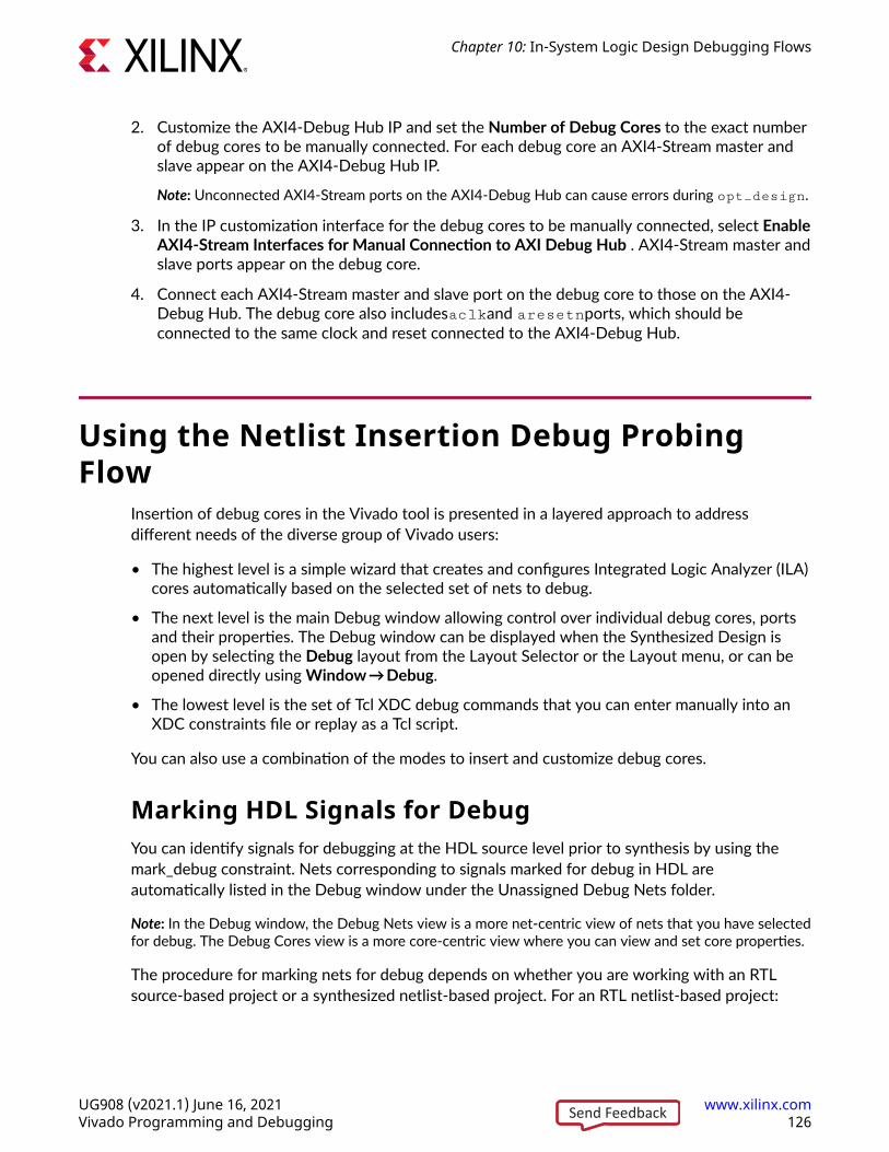
2. Customize the AXI4-Debug Hub IP and set the Number of Debug Cores to the exact numberof debug cores to be manually connected. For each debug core an AXI4-Stream master andslave appear on the AXI4-Debug Hub IP.
Note: Unconnected AXI4-Stream ports on the AXI4-Debug Hub can cause errors during opt_design.
3. In the IP customization interface for the debug cores to be manually connected, select EnableAXI4-Stream Interfaces for Manual Connection to AXI Debug Hub . AXI4-Stream master andslave ports appear on the debug core.
4. Connect each AXI4-Stream master and slave port on the debug core to those on the AXI4-Debug Hub. The debug core also includesaclkand aresetnports, which should beconnected to the same clock and reset connected to the AXI4-Debug Hub.
Using the Netlist Insertion Debug ProbingFlow
Insertion of debug cores in the Vivado tool is presented in a layered approach to addressdifferent needs of the diverse group of Vivado users:
• The highest level is a simple wizard that creates and configures Integrated Logic Analyzer (ILA)cores automatically based on the selected set of nets to debug.
• The next level is the main Debug window allowing control over individual debug cores, portsand their properties. The Debug window can be displayed when the Synthesized Design isopen by selecting the Debug layout from the Layout Selector or the Layout menu, or can beopened directly using Window → Debug.
• The lowest level is the set of Tcl XDC debug commands that you can enter manually into anXDC constraints file or replay as a Tcl script.
You can also use a combination of the modes to insert and customize debug cores.
Marking HDL Signals for DebugYou can identify signals for debugging at the HDL source level prior to synthesis by using themark_debug constraint. Nets corresponding to signals marked for debug in HDL areautomatically listed in the Debug window under the Unassigned Debug Nets folder.
Note: In the Debug window, the Debug Nets view is a more net-centric view of nets that you have selectedfor debug. The Debug Cores view is a more core-centric view where you can view and set core properties.
The procedure for marking nets for debug depends on whether you are working with an RTLsource-based project or a synthesized netlist-based project. For an RTL netlist-based project:
Chapter 10: In-System Logic Design Debugging Flows
UG908 (v2021.1) June 16, 2021 www.xilinx.comVivado Programming and Debugging 126Send Feedback
• Using the Vivado synthesis feature you can optionally mark HDL signals for debug using themark_debug constraint in VHDL and Verilog source files. The valid values for the mark_debugconstraint are "TRUE" or “FALSE”. The Vivado synthesis feature does not support the “SOFT”value.
For a synthesized netlist-based project:
• Using the Synopsys® Synplify® synthesis tool, you can optionally mark nets for debug usingthe mark_debug and syn_keep constraints in VHDL or Verilog, or using the mark_debugconstraint alone in the Synopsys Design Constraints (SDC) file. Synplify does not support the“SOFT” value, as this behavior is controlled by the syn_keep attribute.
• Using the Mentor Graphics® Precision® synthesis tool, you can optionally mark nets for debugusing the mark_debug constraint in VHDL or Verilog.
The following subsections provide syntactical examples for Vivado synthesis, XST, Synplify, andPrecision source files.
Icons and ILA Core
• The hollow green icon indicates nets with MARK_DEBUG property set, but not connectedto any ILA core.
• The full green icon indicates nets with MARK_DEBUG property set, and connected to anILA core.
• The yellow icon indicates that there is no MARK_DEBUG on the net, but it is connected toan ILA core.
Vivado Synthesis mark_debug Syntax ExamplesThe following are examples of VHDL and Verilog syntax when using Vivado synthesis.
• VHDL Syntax Example
attribute mark_debug : string;attribute mark_debug of char_fifo_dout: signal is "true";
• Verilog Syntax Example
(* mark_debug = "true" *) wire [7:0] char_fifo_dout;
Synplify mark_debug Syntax ExamplesThe following are examples of Synplify syntax for VHDL, Verilog, and SDC.
Chapter 10: In-System Logic Design Debugging Flows
UG908 (v2021.1) June 16, 2021 www.xilinx.comVivado Programming and Debugging 127Send Feedback

• VHDL Syntax Example
attribute syn_keep : boolean;attribute mark_debug : string;attribute syn_keep of char_fifo_dout: signal is true;attribute mark_debug of char_fifo_dout: signal is "true";
• Verilog Syntax Example
(* syn_keep = "true", mark_debug = "true" *) wire [7:0] char_fifo_dout;
• SDC Syntax Example
define_attribute {n:char_fifo_din[*]} {mark_debug} {"true"}define_attribute {n:char_fifo_din[*]} {syn_keep} {"true"}
IMPORTANT! Net names in an SDC source must be prefixed with the "n:" qualifier.
Note: Synopsys Design Constraints (SDC) is an accepted industry standard for communicating designintent to tools, particularly for timing analysis. A reference copy of the SDC specification is availablefrom Synopsys by registering for the TAP-in program at: https://www.synopsys.com/Community/Interoperability/Pages/TapinSDC.aspx
Precision mark_debug Syntax ExamplesThe following are examples of VHDL and Verilog syntax when using Precision.
• VHDL Syntax Example
attribute mark_debug : string;attribute mark_debug of char_fifo_dout: signal is "true";
• Verilog Syntax Example
(* mark_debug = "true" *) wire [7:0] char_fifo_dout;
Synthesizing the DesignThe next step is to synthesize the design containing the debug cores by clicking Run Synthesis inthe Vivado Design Suite or by running the following Tcl commands:
launch_runs synth_1wait_on_run synth_1
You can also use the synth_design Tcl command to synthesize the design. Refer to the VivadoDesign Suite User Guide: Synthesis (UG901) for more details on the various ways you cansynthesize your design.
Chapter 10: In-System Logic Design Debugging Flows
UG908 (v2021.1) June 16, 2021 www.xilinx.comVivado Programming and Debugging 128Send Feedback
Marking Nets for Debug in the Synthesized DesignOpen the synthesized design by clicking Open Synthesized Design in the Flow Navigator andselect the Debug window layout to see the Debug window. Any nets that correspond to HDLsignals that were marked for debugging are shown in the Unassigned Debug Nets folder in theDebug window.
Figure 77: Unassigned Debug Nets
• Selecting a net in any of the design views (such as the Netlist or Schematic windows), thenright-click select the Mark Debug option.
• Selecting a net in any of the design views, then dragging and dropping the nets into theUnassigned Debug Nets folder.
• Using the net selector in the Set up Debug wizard (see Using the Set Up Debug Wizard toInsert Debug Cores for details).
Related Information
Using the Set Up Debug Wizard to Insert Debug Cores
Using the Set Up Debug Wizard to Insert DebugCoresThe next step after marking nets for debugging is to assign them to debug cores. The VivadoDesign Suite provides an easy to use Set up Debug wizard to help guide you through the processof automatically creating the debug cores and assigning the debug nets to the inputs of thecores.
To use the Set up Debug wizard to insert the debug cores:
1. Optionally, select a set of nets for debugging either using the unassigned nets list or directnet selection.
2. Select Tools → Set up Debug from the Vivado Design Suite main menu, or click Set up Debugin the Flow Navigator under the Synthesized Design section.
Chapter 10: In-System Logic Design Debugging Flows
UG908 (v2021.1) June 16, 2021 www.xilinx.comVivado Programming and Debugging 129Send Feedback
3. Click Next to get to the Specify Nets to Debug panel (see the following figure).
4. Optionally, click Find Nets to Add to add more nets or remove existing nets from the table.You can also right-click a debug net and select Remove Nets to remove nets from the table.
IMPORTANT! You can also select nets in the Netlist or other windows, then drag them to the list ofNets to Debug.
5. Right-click a debug net and select Select Clock Domain to change the clock domain to beused to sample value on the net.
Note: The Set up Debug wizard attempts to automatically select the appropriate clock domain for thedebug net by searching the path for synchronous elements. Use the Select Clock Domain dialogwindow to modify this selection as needed, but be aware that each clock domain present in the tableresults in a separate ILA core instance.
TIP: Refer to ILA Core and Timing Considerations in UltraFast Design Methodology Guide for XilinxFPGAs and SoCs (UG949) for tips on helping to minimize timing impact of the ILA Core.
6. Once you are satisfied with the debug net selection, click Next.
Note: The Set up Debug wizard inserts one ILA core per clock domain. The nets that were selected fordebug are assigned automatically to the probe ports of the inserted ILA cores. The last wizard screenshows the core creation summary displaying the number of clocks found and ILA cores to be createdand/or removed.
7. If you want to enable either advanced trigger mode or basic capture mode, use thecorresponding check boxes to do so. Click Next to move to the last panel.
Note: The advanced trigger mode and basic capture mode features, when used in the Vivado HardwareManager, are described in more detail in Debugging Logic Designs in Hardware.
8. If you are satisfied with the results, click Finish to insert and connect the ILA cores in yoursynthesized design netlist.
Chapter 10: In-System Logic Design Debugging Flows
UG908 (v2021.1) June 16, 2021 www.xilinx.comVivado Programming and Debugging 130Send Feedback
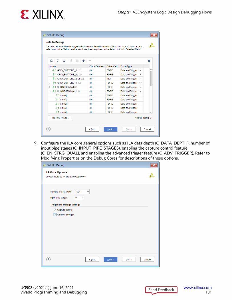
9. Configure the ILA core general options such as ILA data depth (C_DATA_DEPTH), number ofinput pipe stages (C_INPUT_PIPE_STAGES), enabling the capture control feature(C_EN_STRG_QUAL), and enabling the advanced trigger feature (C_ADV_TRIGGER). Refer toModifying Properties on the Debug Cores for descriptions of these options.
Chapter 10: In-System Logic Design Debugging Flows
UG908 (v2021.1) June 16, 2021 www.xilinx.comVivado Programming and Debugging 131Send Feedback

10. The debug nets are now assigned to the ILA debug core, as shown in the following figure.
Related Information
ILA Core and Timing ConsiderationsDebugging Logic Designs in HardwareModifying Properties on the Debug Cores
Using the Debug Window to Add and CustomizeDebug CoresThe Debug Cores tab in the Debug window provides more fine-grained control over ILA core anddebug core hub insertion than what is available in the Set up Debug wizard. The controlsavailable in this window allow core creation, core deletion, debug net connection, and coreparameter changes.
The Debug Cores tab of the Debug window:
• Shows the list of debug cores that are connected to the Debug Hub (dbg_hub) core.
• Maintains the list of unassigned debug nets at the bottom of the window.
You can manipulate debug cores and ports from the popup menu or the toolbar buttons on thetop of the window.
Creating and Removing Debug CoresTo create debug cores in the Debug window, click Create Debug Core. Using this interface, youcan change the parent instance, debug core name, and set parameters for the core. To remove anexisting debug core, right-click the core in the Debug window and select Delete. Refer toModifying Properties on the Debug Cores for a description of the ILA core options found in theCreate Debug Core dialog.
Chapter 10: In-System Logic Design Debugging Flows
UG908 (v2021.1) June 16, 2021 www.xilinx.comVivado Programming and Debugging 132Send Feedback
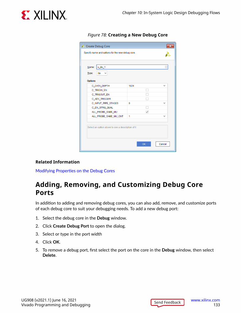
Figure 78: Creating a New Debug Core
Related Information
Modifying Properties on the Debug Cores
Adding, Removing, and Customizing Debug CorePortsIn addition to adding and removing debug cores, you can also add, remove, and customize portsof each debug core to suit your debugging needs. To add a new debug port:
1. Select the debug core in the Debug window.
2. Click Create Debug Port to open the dialog.
3. Select or type in the port width
4. Click OK.
5. To remove a debug port, first select the port on the core in the Debug window, then selectDelete.
Chapter 10: In-System Logic Design Debugging Flows
UG908 (v2021.1) June 16, 2021 www.xilinx.comVivado Programming and Debugging 133Send Feedback
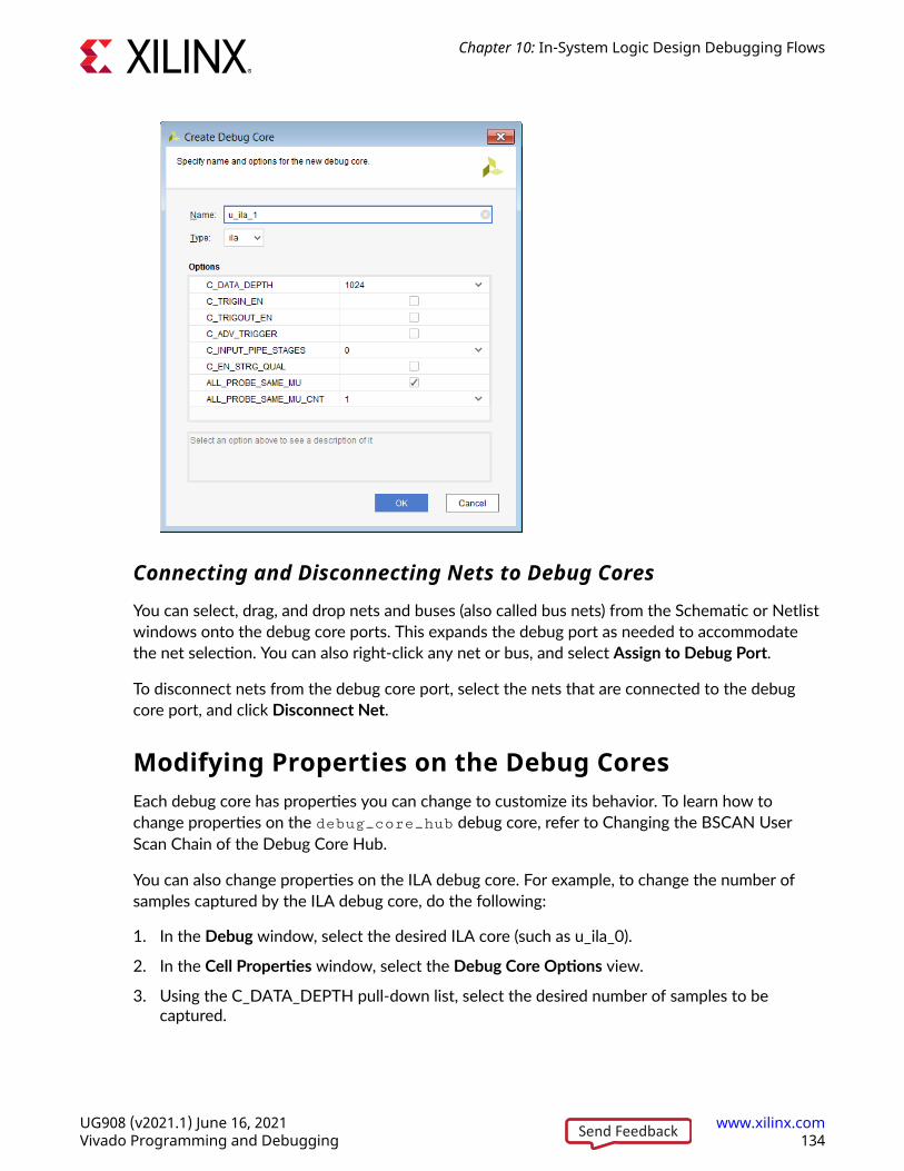
Connecting and Disconnecting Nets to Debug Cores
You can select, drag, and drop nets and buses (also called bus nets) from the Schematic or Netlistwindows onto the debug core ports. This expands the debug port as needed to accommodatethe net selection. You can also right-click any net or bus, and select Assign to Debug Port.
To disconnect nets from the debug core port, select the nets that are connected to the debugcore port, and click Disconnect Net.
Modifying Properties on the Debug CoresEach debug core has properties you can change to customize its behavior. To learn how tochange properties on the debug_core_hub debug core, refer to Changing the BSCAN UserScan Chain of the Debug Core Hub.
You can also change properties on the ILA debug core. For example, to change the number ofsamples captured by the ILA debug core, do the following:
1. In the Debug window, select the desired ILA core (such as u_ila_0).
2. In the Cell Properties window, select the Debug Core Options view.
3. Using the C_DATA_DEPTH pull-down list, select the desired number of samples to becaptured.
Chapter 10: In-System Logic Design Debugging Flows
UG908 (v2021.1) June 16, 2021 www.xilinx.comVivado Programming and Debugging 134Send Feedback
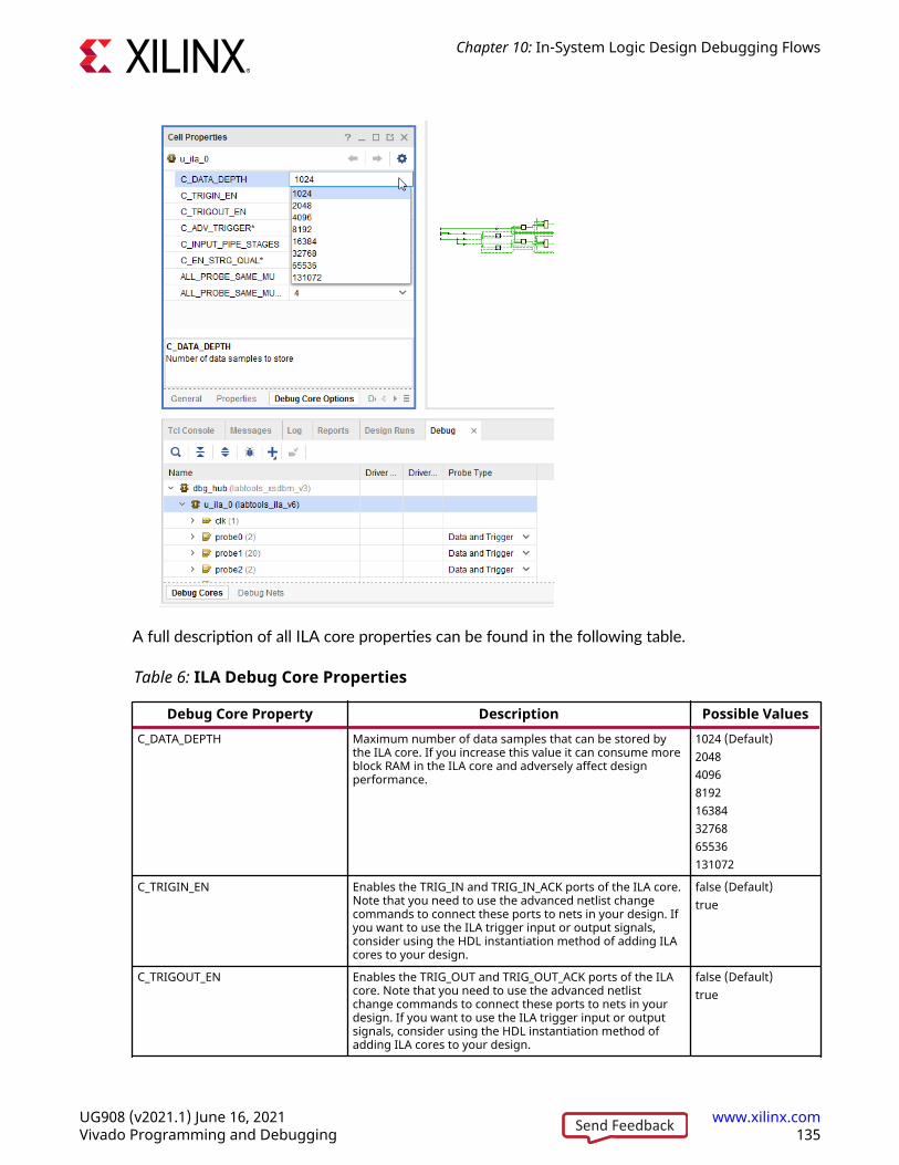
A full description of all ILA core properties can be found in the following table.
Table 6: ILA Debug Core Properties
Debug Core Property Description Possible ValuesC_DATA_DEPTH Maximum number of data samples that can be stored by
the ILA core. If you increase this value it can consume moreblock RAM in the ILA core and adversely affect designperformance.
1024 (Default)204840968192163843276865536131072
C_TRIGIN_EN Enables the TRIG_IN and TRIG_IN_ACK ports of the ILA core.Note that you need to use the advanced netlist changecommands to connect these ports to nets in your design. Ifyou want to use the ILA trigger input or output signals,consider using the HDL instantiation method of adding ILAcores to your design.
false (Default)true
C_TRIGOUT_EN Enables the TRIG_OUT and TRIG_OUT_ACK ports of the ILAcore. Note that you need to use the advanced netlistchange commands to connect these ports to nets in yourdesign. If you want to use the ILA trigger input or outputsignals, consider using the HDL instantiation method ofadding ILA cores to your design.
false (Default)true
Chapter 10: In-System Logic Design Debugging Flows
UG908 (v2021.1) June 16, 2021 www.xilinx.comVivado Programming and Debugging 135Send Feedback
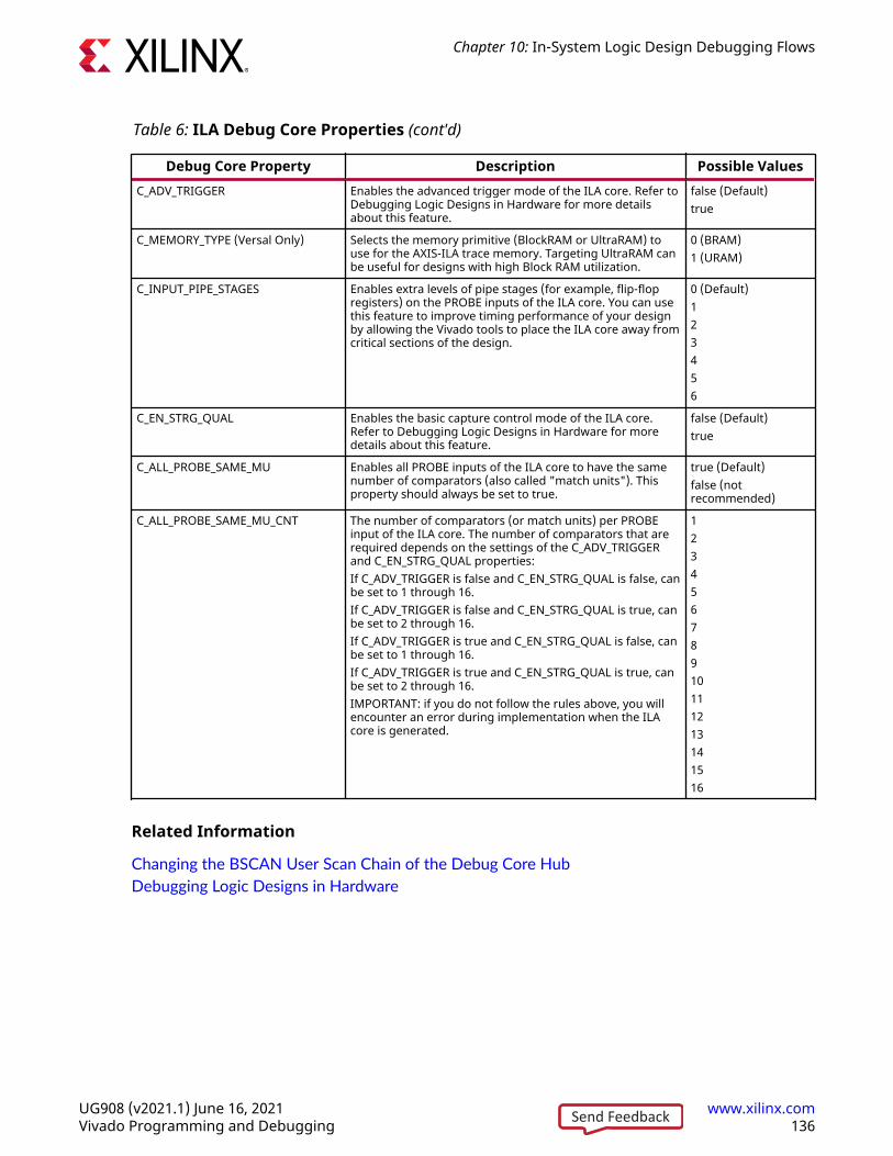
Table 6: ILA Debug Core Properties (cont'd)
Debug Core Property Description Possible ValuesC_ADV_TRIGGER Enables the advanced trigger mode of the ILA core. Refer to
Debugging Logic Designs in Hardware for more detailsabout this feature.
false (Default)true
C_MEMORY_TYPE (Versal Only) Selects the memory primitive (BlockRAM or UltraRAM) touse for the AXIS-ILA trace memory. Targeting UltraRAM canbe useful for designs with high Block RAM utilization.
0 (BRAM)1 (URAM)
C_INPUT_PIPE_STAGES Enables extra levels of pipe stages (for example, flip-flopregisters) on the PROBE inputs of the ILA core. You can usethis feature to improve timing performance of your designby allowing the Vivado tools to place the ILA core away fromcritical sections of the design.
0 (Default)123456
C_EN_STRG_QUAL Enables the basic capture control mode of the ILA core.Refer to Debugging Logic Designs in Hardware for moredetails about this feature.
false (Default)true
C_ALL_PROBE_SAME_MU Enables all PROBE inputs of the ILA core to have the samenumber of comparators (also called "match units"). Thisproperty should always be set to true.
true (Default)false (notrecommended)
C_ALL_PROBE_SAME_MU_CNT The number of comparators (or match units) per PROBEinput of the ILA core. The number of comparators that arerequired depends on the settings of the C_ADV_TRIGGERand C_EN_STRG_QUAL properties:If C_ADV_TRIGGER is false and C_EN_STRG_QUAL is false, canbe set to 1 through 16.If C_ADV_TRIGGER is false and C_EN_STRG_QUAL is true, canbe set to 2 through 16.If C_ADV_TRIGGER is true and C_EN_STRG_QUAL is false, canbe set to 1 through 16.If C_ADV_TRIGGER is true and C_EN_STRG_QUAL is true, canbe set to 2 through 16.IMPORTANT: if you do not follow the rules above, you willencounter an error during implementation when the ILAcore is generated.
12345678910111213141516
Related Information
Changing the BSCAN User Scan Chain of the Debug Core HubDebugging Logic Designs in Hardware
Chapter 10: In-System Logic Design Debugging Flows
UG908 (v2021.1) June 16, 2021 www.xilinx.comVivado Programming and Debugging 136Send Feedback
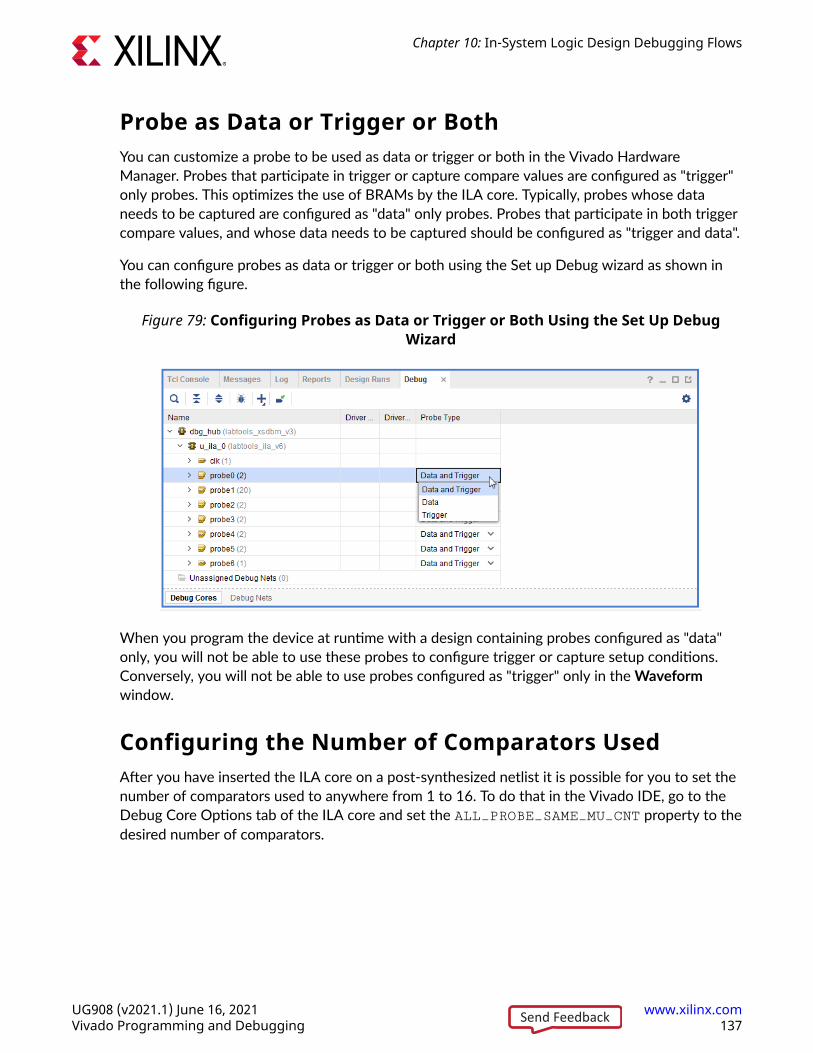
Probe as Data or Trigger or BothYou can customize a probe to be used as data or trigger or both in the Vivado HardwareManager. Probes that participate in trigger or capture compare values are configured as "trigger"only probes. This optimizes the use of BRAMs by the ILA core. Typically, probes whose dataneeds to be captured are configured as "data" only probes. Probes that participate in both triggercompare values, and whose data needs to be captured should be configured as "trigger and data".
You can configure probes as data or trigger or both using the Set up Debug wizard as shown inthe following figure.
Figure 79: Configuring Probes as Data or Trigger or Both Using the Set Up DebugWizard
When you program the device at runtime with a design containing probes configured as "data"only, you will not be able to use these probes to configure trigger or capture setup conditions.Conversely, you will not be able to use probes configured as "trigger" only in the Waveformwindow.
Configuring the Number of Comparators UsedAfter you have inserted the ILA core on a post-synthesized netlist it is possible for you to set thenumber of comparators used to anywhere from 1 to 16. To do that in the Vivado IDE, go to theDebug Core Options tab of the ILA core and set the ALL_PROBE_SAME_MU_CNT property to thedesired number of comparators.
Chapter 10: In-System Logic Design Debugging Flows
UG908 (v2021.1) June 16, 2021 www.xilinx.comVivado Programming and Debugging 137Send Feedback
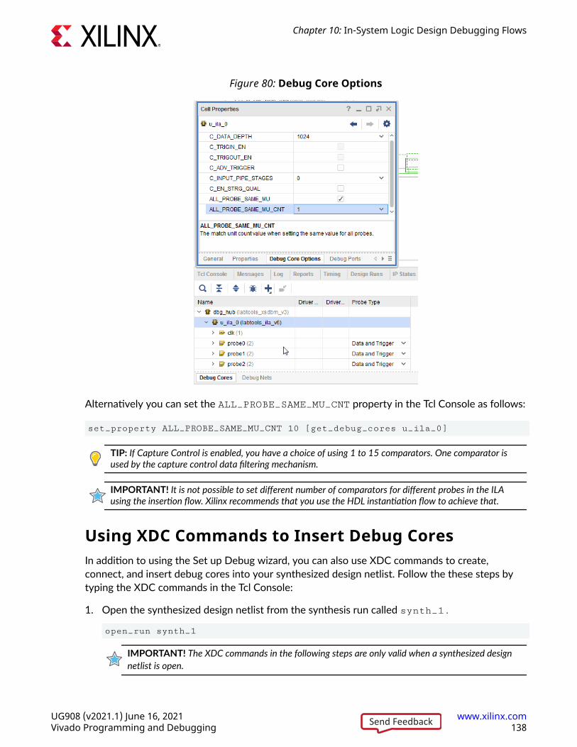
Figure 80: Debug Core Options
Alternatively you can set the ALL_PROBE_SAME_MU_CNT property in the Tcl Console as follows:
set_property ALL_PROBE_SAME_MU_CNT 10 [get_debug_cores u_ila_0]
TIP: If Capture Control is enabled, you have a choice of using 1 to 15 comparators. One comparator isused by the capture control data filtering mechanism.
IMPORTANT! It is not possible to set different number of comparators for different probes in the ILAusing the insertion flow. Xilinx recommends that you use the HDL instantiation flow to achieve that.
Using XDC Commands to Insert Debug CoresIn addition to using the Set up Debug wizard, you can also use XDC commands to create,connect, and insert debug cores into your synthesized design netlist. Follow the these steps bytyping the XDC commands in the Tcl Console:
1. Open the synthesized design netlist from the synthesis run called synth_1.
open_run synth_1
IMPORTANT! The XDC commands in the following steps are only valid when a synthesized designnetlist is open.
Chapter 10: In-System Logic Design Debugging Flows
UG908 (v2021.1) June 16, 2021 www.xilinx.comVivado Programming and Debugging 138Send Feedback
2. Create the ILA core black box.
create_debug_core u_ila_0 ila
3. Set the various properties of the ILA core.
set_property C_DATA_DEPTH 1024 [get_debug_cores u_ila_0]set_property C_TRIGIN_EN false [get_debug_cores u_ila_0]set_property C_TRIGOUT_EN false [get_debug_cores u_ila_0]set_property C_ADV_TRIGGER false [get_debug_cores u_ila_0]set_property C_INPUT_PIPE_STAGES 0 [get_debug_cores u_ila_0]set_property C_EN_STRG_QUAL false [get_debug_cores u_ila_0]set_property ALL_PROBE_SAME_MU true [get_debug_cores u_ila_0]set_property ALL_PROBE_SAME_MU_CNT 1 [get_debug_cores u_ila_0]
4. Set the width of the clk port of the ILA core to 1 and connect it to the desired clock net.
set_property port_width 1 [get_debug_ports u_ila_0/clk]connect_debug_port u_ila_0/clk [get_nets [list clk ]]
Note: You do not have to create the clk port of the ILA core because it is automatically created by thecreate_debug_core command.
IMPORTANT! All debug port names of the debug cores are lower case. Using upper-case or mixed-case debug port names will result in an error.
5. Set the width of the probe0 port to the number of nets you plan to connect to the port.
Note: You do not have to create the first probe port (probe0) of the ILA core because it is automaticallycreated by the create_debug_core command. set_property port_width 1 [get_debug_ports u_ila_0/probe0]
6. Connect the probe0 port to the nets you want to attach to that port.
connect_debug_port u_ila_0/probe0 [get_nets [list A_or_B]]
7. Optionally, create more probe ports, set their width, and connect them to the nets you wantto debug.
create_debug_port u_ila_0 probeset_property port_width 2 [get_debug_ports u_ila_0/probe1]connect_debug_port u_ila_0/probe1 [get_nets [list {A[0]} {A[1]}]]
For more information on these and other related Tcl commands, type help -categoryChipScope in the Tcl Console of the Vivado Design Suite.
Saving Constraints After Running Debug XDCCommandsYou need to save constraints after using the Set up Debug wizard, using Vivado Design Suite tocreate debug cores or ports, and/or running the following XDC commands:
Chapter 10: In-System Logic Design Debugging Flows
UG908 (v2021.1) June 16, 2021 www.xilinx.comVivado Programming and Debugging 139Send Feedback

• create_debug_core
• create_debug_port
• connect_debug_port
• set_property (on any debug_core or debug_port object)
The corresponding XDC commands are saved to a constraints file with the suffix _debug.xdcand are used during implementation to insert and connect the debug cores.
IMPORTANT! Saving constraints while in project mode may cause the synthesis and implementationsteps to go out-of-date. However, you do not need to re-synthesize the design since the debug XDCconstraints are only used during implementation. You can force the synthesis step up-to-date by selectingthe Design Runs window, right-clicking the synthesis run (for example, synth_1), and selecting Force up-to-date.
Implementing the DesignAfter inserting, connecting and customizing your debug cores, you are now ready forimplementing your design (refer to Implementing the Design Containing the Debug Cores).
Related Information
Implementing the Design Containing the Debug Cores
Debug Core Insertion in Non-Project ModeDebug cores can be inserted in either Project Mode or Non-Project Mode. The following sampleTcl script shows how to create the debug core, set debug core attributes, and connect the debugcore probes to the signals in the design being probed. In Non-Project Mode, the insertion of thedebug core needs to happen after synthesizing the design, and prior to the opt_design step asshown below.
IMPORTANT! Debug core insertion is only supported for ILA cores.
The following Tcl script is an example of using the debug core insertion commands in a Non-Project flow.
#read relevant design source filesread_vhdl [glob ./*.vhdl] read_verilog [ glob ./Sources/*.v ]read_xdc ./target.xdc#Synthesize Designsynth_design -top top -part xc7k325tffg900-2 #Create the debug core create_debug_core u_ila_0 ila#set debug core propertiesset_property C_DATA_DEPTH 1024 [get_debug_cores u_ila_0]set_property C_TRIGIN_EN false [get_debug_cores u_ila_0]
Chapter 10: In-System Logic Design Debugging Flows
UG908 (v2021.1) June 16, 2021 www.xilinx.comVivado Programming and Debugging 140Send Feedback
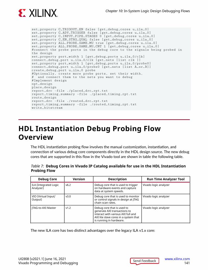
set_property C_TRIGOUT_EN false [get_debug_cores u_ila_0]set_property C_ADV_TRIGGER false [get_debug_cores u_ila_0]set_property C_INPUT_PIPE_STAGES 0 [get_debug_cores u_ila_0]set_property C_EN_STRG_QUAL false [get_debug_cores u_ila_0]set_property ALL_PROBE_SAME_MU true [get_debug_cores u_ila_0]set_property ALL_PROBE_SAME_MU_CNT 1 [get_debug_cores u_ila_0]#connect the probe ports in the debug core to the signals being probed in the designset_property port_width 1 [get_debug_ports u_ila_0/clk]connect_debug_port u_ila_0/clk [get_nets [list clk ]]set_property port_width 1 [get_debug_ports u_ila_0/probe0]connect_debug_port u_ila_0/probe0 [get_nets [list A_or_B]]create_debug_port u_ila_0 probe#Optionally, create more probe ports, set their width, # and connect them to the nets you want to debug#Implement designopt_design place_design report_drc -file ./placed_drc_rpt.txtreport_timing_summary -file ./placed_timing_rpt.txtroute_design report_drc -file ./routed_drc_rpt.txtreport_timing_summary -file ./routed_timing_rpt.txtwrite_bitstream
HDL Instantiation Debug Probing FlowOverview
The HDL instantiation probing flow involves the manual customization, instantiation, andconnection of various debug core components directly in the HDL design source. The new debugcores that are supported in this flow in the Vivado tool are shown in table the following table.
Table 7: Debug Cores in Vivado IP Catalog available for use in the HDL InstantiationProbing Flow
Debug Core Version Description Run Time Analyzer ToolILA (Integrated LogicAnalyzer)
v6.2 Debug core that is used to triggeron hardware events and capturedata at system speeds.
Vivado logic analyzer
VIO (Virtual Input/Output)
v3.0 Debug core that is used to monitoror control signals in design at JTAGchain scan rates.
Vivado logic analyzer
JTAG-to-AXI Master v1.2 Debug core that is used togenerate AXI transactions tointeract with various AXI full andAXI lite slave cores in a system thatis running in hardware.
Vivado logic analyzer
The new ILA core has two distinct advantages over the legacy ILA v1.x core:
Chapter 10: In-System Logic Design Debugging Flows
UG908 (v2021.1) June 16, 2021 www.xilinx.comVivado Programming and Debugging 141Send Feedback
• Works with the integrated Vivado logic analyzer feature (refer to Debugging Logic Designs inHardware).
• No ICON core instance or connection is required.
Related Information
Debugging Logic Designs in Hardware
Using the HDL Instantiation Debug ProbingFlow
The steps required to perform the HDL instantiation flow are:
1. Customize and generate the ILA and/or VIO debug cores that have the right number of probeports for the signals you want to probe.
2. (Optional) Customize and generate the JTAG-to-AXI Master debug core and connect it to anAXI slave interface of an AXI peripheral or interconnect core in your design.
3. Synthesize the design containing the debug cores.
4. (Optional) Modify debug hub core properties.
5. Implement the design containing the debug cores.
Customizing and Generating the Debug CoresUse the IP Catalog button in the Project Manager to locate, select, and customize the desireddebug core. The debug cores are located in the Debug & Verification > Debug category of the IPCatalog (see the following figure). You can customize the debug core by double-clicking on the IPcore or by right-click selecting the Customize IP menu selection.
• For more information on customizing the ILA core, refer to Integrated Logic Analyzer LogiCOREIP Product Guide (PG172) .
• For more information on customizing the VIO core, refer to Virtual Input/Output LogiCORE IPProduct Guide (PG159).
• For more information on customizing the JTAG-to-AXI Master core, refer to JTAG to AXIMaster LogiCORE IP Product Guide (PG174).
After customizing the core, click the Generate button in the IP customization wizard. Thisgenerates the customized debug core and add it to the Sources view of your project.
Chapter 10: In-System Logic Design Debugging Flows
UG908 (v2021.1) June 16, 2021 www.xilinx.comVivado Programming and Debugging 142Send Feedback
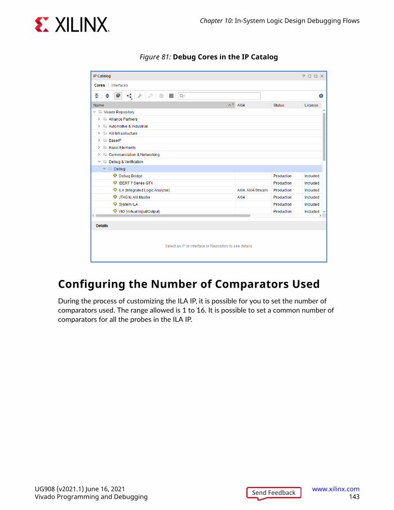
Figure 81: Debug Cores in the IP Catalog
Configuring the Number of Comparators UsedDuring the process of customizing the ILA IP, it is possible for you to set the number ofcomparators used. The range allowed is 1 to 16. It is possible to set a common number ofcomparators for all the probes in the ILA IP.
Chapter 10: In-System Logic Design Debugging Flows
UG908 (v2021.1) June 16, 2021 www.xilinx.comVivado Programming and Debugging 143Send Feedback
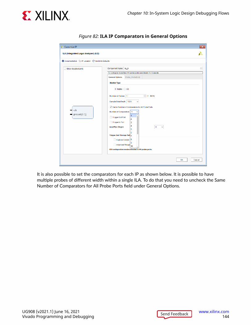
Figure 82: ILA IP Comparators in General Options
It is also possible to set the comparators for each IP as shown below. It is possible to havemultiple probes of different width within a single ILA. To do that you need to uncheck the SameNumber of Comparators for All Probe Ports field under General Options.
Chapter 10: In-System Logic Design Debugging Flows
UG908 (v2021.1) June 16, 2021 www.xilinx.comVivado Programming and Debugging 144Send Feedback
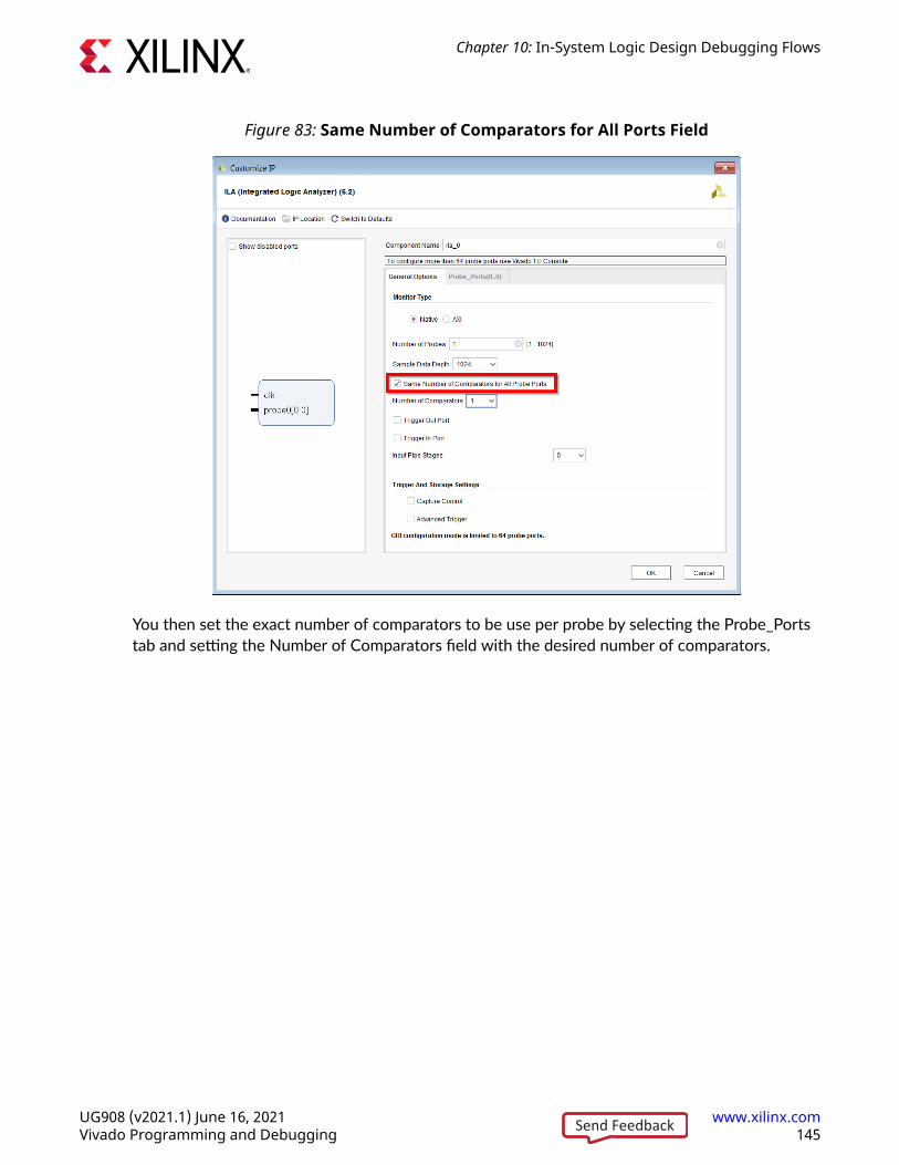
Figure 83: Same Number of Comparators for All Ports Field
You then set the exact number of comparators to be use per probe by selecting the Probe_Portstab and setting the Number of Comparators field with the desired number of comparators.
Chapter 10: In-System Logic Design Debugging Flows
UG908 (v2021.1) June 16, 2021 www.xilinx.comVivado Programming and Debugging 145Send Feedback
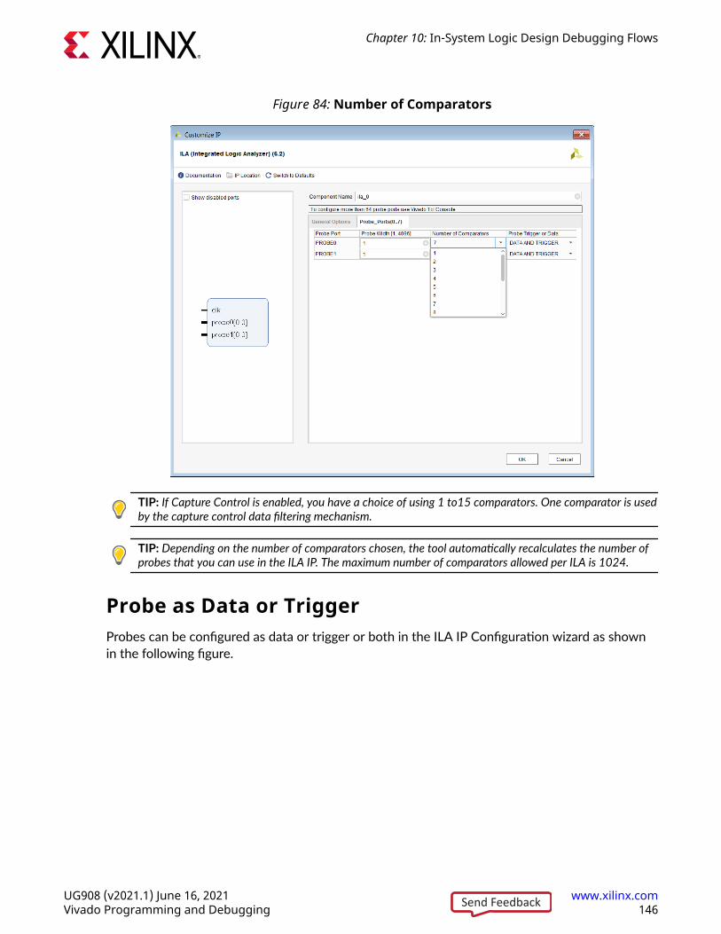
Figure 84: Number of Comparators
TIP: If Capture Control is enabled, you have a choice of using 1 to15 comparators. One comparator is usedby the capture control data filtering mechanism.
TIP: Depending on the number of comparators chosen, the tool automatically recalculates the number ofprobes that you can use in the ILA IP. The maximum number of comparators allowed per ILA is 1024.
Probe as Data or TriggerProbes can be configured as data or trigger or both in the ILA IP Configuration wizard as shownin the following figure.
Chapter 10: In-System Logic Design Debugging Flows
UG908 (v2021.1) June 16, 2021 www.xilinx.comVivado Programming and Debugging 146Send Feedback
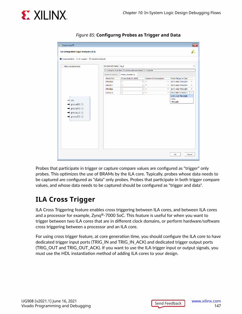
Figure 85: Configurng Probes as Trigger and Data
Probes that participate in trigger or capture compare values are configured as "trigger" onlyprobes. This optimizes the use of BRAMs by the ILA core. Typically, probes whose data needs tobe captured are configured as "data" only probes. Probes that participate in both trigger comparevalues, and whose data needs to be captured should be configured as "trigger and data".
ILA Cross TriggerILA Cross Triggering feature enables cross triggering between ILA cores, and between ILA coresand a processor for example, Zynq®-7000 SoC. This feature is useful for when you want totrigger between two ILA cores that are in different clock domains, or perform hardware/softwarecross triggering between a processor and an ILA core.
For using cross trigger feature, at core generation time, you should configure the ILA core to havededicated trigger input ports (TRIG_IN and TRIG_IN_ACK) and dedicated trigger output ports(TRIG_OUT and TRIG_OUT_ACK). If you want to use the ILA trigger input or output signals, youmust use the HDL instantiation method of adding ILA cores to your design.
Chapter 10: In-System Logic Design Debugging Flows
UG908 (v2021.1) June 16, 2021 www.xilinx.comVivado Programming and Debugging 147Send Feedback
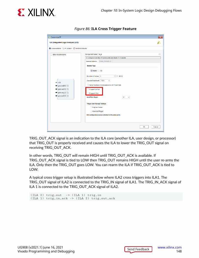
Figure 86: ILA Cross Trigger Feature
TRIG_OUT_ACK signal is an indication to the ILA core (another ILA, user design, or processor)that TRIG_OUT is properly received and causes the ILA to lower the TRIG_OUT signal onreceiving TRIG_OUT_ACK.
In other words, TRIG_OUT will remain HIGH until TRIG_OUT_ACK is available. IfTRIG_OUT_ACK signal is tied to LOW then TRIG_OUT remains HIGH until the user re-arms theILA. Only then the TRIG_OUT goes LOW. You can rearm the ILA if TRIG_OUT_ACK is tied toLOW.
A typical cross trigger setup is illustrated below where ILA2 cross triggers into ILA1. TheTRIG_OUT signal of ILA2 is connected to the TRIG_IN signal of ILA1. The TRIG_IN_ACK signal ofILA 1 is connected to the TRIG_OUT_ACK signal of ILA2.
(ILA 2) trig_out -> (ILA 1) trig_in (ILA 1) trig_in_ack -> (ILA 2) trig_out_ack
Chapter 10: In-System Logic Design Debugging Flows
UG908 (v2021.1) June 16, 2021 www.xilinx.comVivado Programming and Debugging 148Send Feedback

Figure 87: Typical Cross Trigger Setup
ILA 1 ILA 2
trig_in
trig_in_ack
trig_out
trig_out_ack
trig_out
trig_out_ack
trig_in
trig_in_ack
X16408-031616
Figure 88: ILA Cross Trigger Timing
• It is assumed that the logic driving the trig_in port is synchronous to the ILA clk.
• It takes 1 clk cycle for the trig_in_ack signal to get asserted after trig_in is asserted.
• It takes 9 clk cycles for the trig_out signal to get asserted when trig_in is used or triggercondition is met.
• The trig_in_ack and trig_out_ack signals go low only when trigger signals are de-asserted.
For a detailed tutorial that covers using the Cross Trigger feature between the FPGA fabric andthe Zynq-7000 SoC processor, see the Vivado Design Suite Tutorial: Embedded Processor HardwareDesign (UG940).
Chapter 10: In-System Logic Design Debugging Flows
UG908 (v2021.1) June 16, 2021 www.xilinx.comVivado Programming and Debugging 149Send Feedback
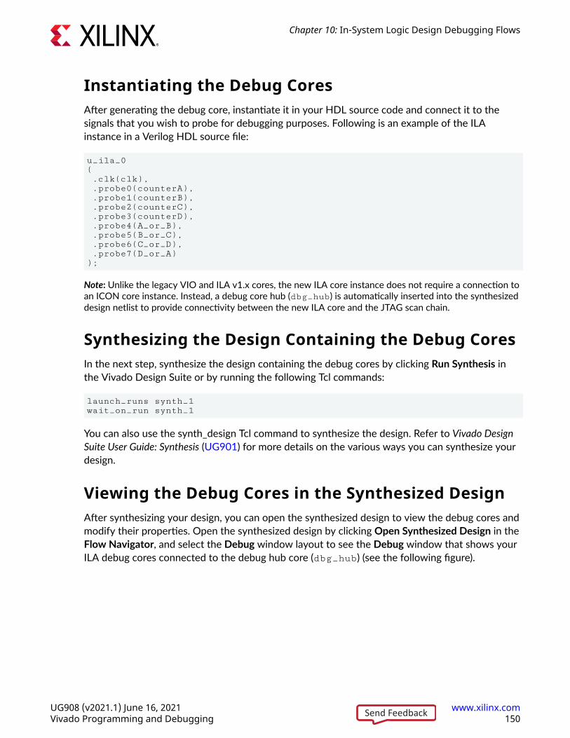
Instantiating the Debug CoresAfter generating the debug core, instantiate it in your HDL source code and connect it to thesignals that you wish to probe for debugging purposes. Following is an example of the ILAinstance in a Verilog HDL source file:
u_ila_0 ( .clk(clk), .probe0(counterA), .probe1(counterB), .probe2(counterC), .probe3(counterD), .probe4(A_or_B), .probe5(B_or_C), .probe6(C_or_D), .probe7(D_or_A));
Note: Unlike the legacy VIO and ILA v1.x cores, the new ILA core instance does not require a connection toan ICON core instance. Instead, a debug core hub (dbg_hub) is automatically inserted into the synthesizeddesign netlist to provide connectivity between the new ILA core and the JTAG scan chain.
Synthesizing the Design Containing the Debug CoresIn the next step, synthesize the design containing the debug cores by clicking Run Synthesis inthe Vivado Design Suite or by running the following Tcl commands:
launch_runs synth_1wait_on_run synth_1
You can also use the synth_design Tcl command to synthesize the design. Refer to Vivado DesignSuite User Guide: Synthesis (UG901) for more details on the various ways you can synthesize yourdesign.
Viewing the Debug Cores in the Synthesized DesignAfter synthesizing your design, you can open the synthesized design to view the debug cores andmodify their properties. Open the synthesized design by clicking Open Synthesized Design in theFlow Navigator, and select the Debug window layout to see the Debug window that shows yourILA debug cores connected to the debug hub core (dbg_hub) (see the following figure).
Chapter 10: In-System Logic Design Debugging Flows
UG908 (v2021.1) June 16, 2021 www.xilinx.comVivado Programming and Debugging 150Send Feedback

Figure 89: Debug Window Showing ILA Core and Debug Core Hub
Changing the BSCAN User Scan Chain of the DebugCore HubYou can view and change the BSCAN user scan chain index of the debug core hub by selectingthe dbg_hub in the Debug window, selecting the Debug Core Options view in the Propertieswindow, then changing the value of the C_USER_SCAN_CHAIN property (see the followingfigure).
IMPORTANT! The default values for C_USER_SCAN_CHAIN is 1 for the debug hub core. If using a scanchain value other than 1 for the debug hub core, you must manually change them on the device in theHardware Manager. Refer to Programming the Hardware Device for more details.
IMPORTANT! If you plan to use the Microprocessor Debug Module (MDM) or other IP that uses theBSCAN primitive with the Vivado logic debug cores, you need to set the C_USER_SCAN_CHAIN propertyof the dbg_hub to a user scan chain that does not conflict with the other IPs Boundary Scan Chainsetting. Failure to do so results in errors later in the implementation flow.
Chapter 10: In-System Logic Design Debugging Flows
UG908 (v2021.1) June 16, 2021 www.xilinx.comVivado Programming and Debugging 151Send Feedback
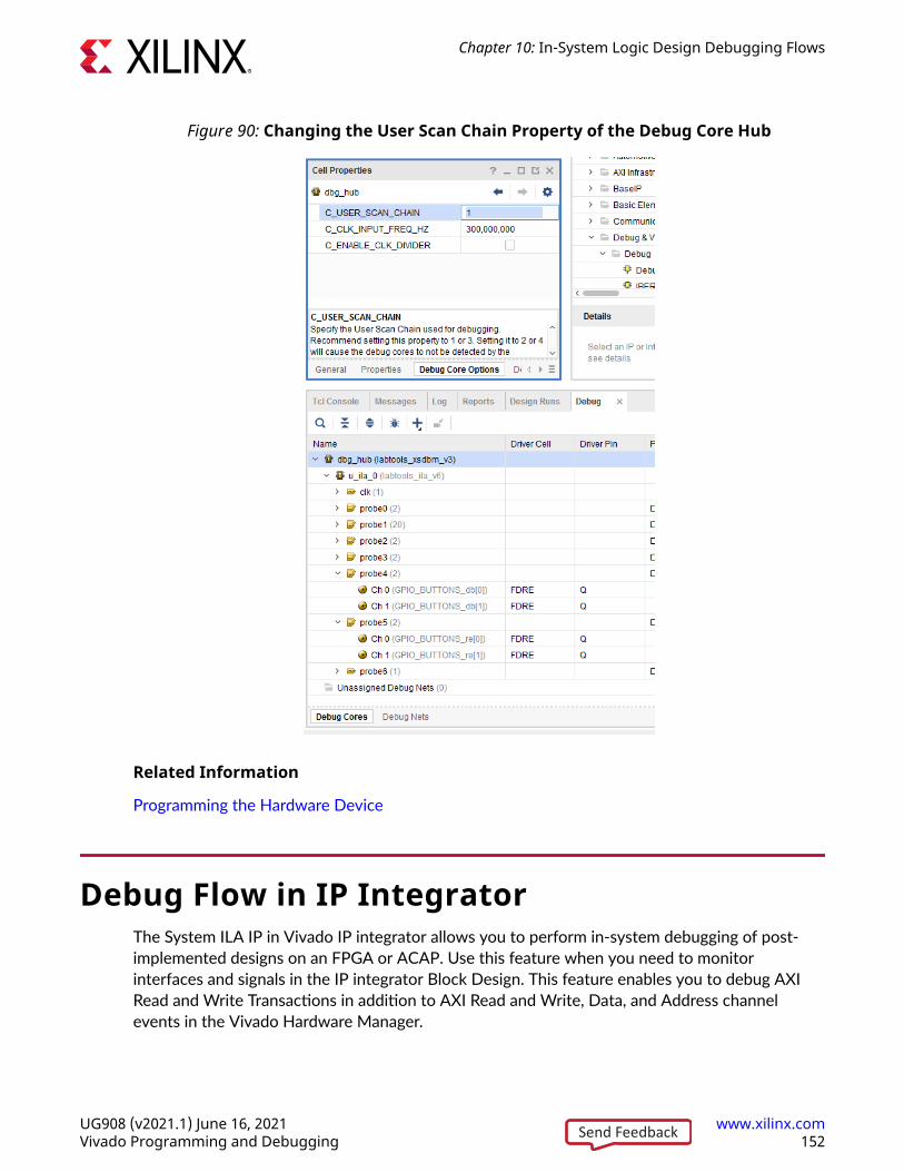
Figure 90: Changing the User Scan Chain Property of the Debug Core Hub
Related Information
Programming the Hardware Device
Debug Flow in IP IntegratorThe System ILA IP in Vivado IP integrator allows you to perform in-system debugging of post-implemented designs on an FPGA or ACAP. Use this feature when you need to monitorinterfaces and signals in the IP integrator Block Design. This feature enables you to debug AXIRead and Write Transactions in addition to AXI Read and Write, Data, and Address channelevents in the Vivado Hardware Manager.
Chapter 10: In-System Logic Design Debugging Flows
UG908 (v2021.1) June 16, 2021 www.xilinx.comVivado Programming and Debugging 152Send Feedback
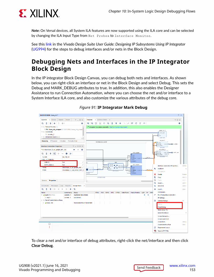
Note: On Versal devices, all System ILA features are now supported using the ILA core and can be selectedby changing the ILA Input Type from Net Probes to Interface Monitor.
See this link in the Vivado Design Suite User Guide: Designing IP Subsystems Using IP Integrator(UG994) for the steps to debug interfaces and/or nets in the Block Design.
Debugging Nets and Interfaces in the IP IntegratorBlock DesignIn the IP integrator Block Design Canvas, you can debug both nets and interfaces. As shownbelow, you can right-click an interface or net in the Block Design and select Debug. This sets theDebug and MARK_DEBUG attributes to true. In addition, this also enables the DesignerAssistance to run Connection Automation, where you can choose the net and/or interface to aSystem Interface ILA core, and also customize the various attributes of the debug core.
Figure 91: IP Integrator Mark Debug
To clear a net and/or interface of debug attributes, right-click the net/interface and then clickClear Debug.
Chapter 10: In-System Logic Design Debugging Flows
UG908 (v2021.1) June 16, 2021 www.xilinx.comVivado Programming and Debugging 153Send Feedback
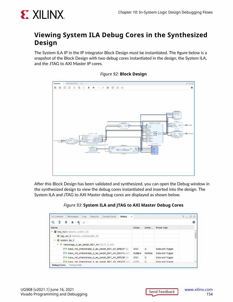
Viewing System ILA Debug Cores in the SynthesizedDesignThe System ILA IP in the IP integrator Block Design must be instantiated. The figure below is asnapshot of the Block Design with two debug cores instantiated in the design, the System ILA,and the JTAG to AXI Master IP cores.
Figure 92: Block Design
After this Block Design has been validated and synthesized, you can open the Debug window inthe synthesized design to view the debug cores instantiated and inserted into the design. TheSystem ILA and JTAG to AXI Master debug cores are displayed as shown below.
Figure 93: System ILA and JTAG to AXI Master Debug Cores
Chapter 10: In-System Logic Design Debugging Flows
UG908 (v2021.1) June 16, 2021 www.xilinx.comVivado Programming and Debugging 154Send Feedback
For more details on how these interfaces can be used for debug in the Hardware Manager and totake advantage of the AXI Event level debug, see Debugging AXI Interfaces in the HardwareManager.
Related Information
Debugging AXI Interfaces in the Hardware Manager
Implementing the Design Containing theDebug Cores
The Vivado software creates the debug core hub initially as a black box. This core must beimplemented prior to running the placer and router.
Implementing the DesignImplement the design containing the debug core by clicking Run Implementation in the VivadoDesign Suite or by running the following Tcl commands:
launch_runs impl_1wait_on_run impl_1
You can also implement the design using the implementation commands opt_design,place_design, and route_design. Refer to the Vivado Design Suite User Guide:Implementation (UG904) for more details on the various ways you can implement your design.
ILA Core and Timing ConsiderationsThe configuration of the ILA core has an impact in meeting the overall design timing goals. Followthe recommendations below to minimize the impact on timing:
• Choose probe width judiciously. The bigger the probe width the greater the impact on bothresource utilization and timing.
• Choose ILA core data depth judiciously. The bigger the data depth, the greater the impact onboth block RAM resource utilization and timing.
• Ensure that the clocks chosen for the ILA cores are free-running clocks. Failure to do so couldresult in an inability to communicate with the debug core when the design is loaded onto thedevice.
Chapter 10: In-System Logic Design Debugging Flows
UG908 (v2021.1) June 16, 2021 www.xilinx.comVivado Programming and Debugging 155Send Feedback
• Close timing on the design prior to adding the debug cores. Xilinx does not recommend usingthe debug cores to debug timing related issues.
• Make sure the clock input to the ILA core is synchronous to the signals being probed. Failureto do so results in timing issues and communication failures with the debug core when thedesign is programmed into the device.
• Make sure that the design meets timing before running it on hardware. Failure to do so resultsin unreliable results.
• For Non-Versal architectures: Ensure that the clock going to the dbg_hub is a free runningclock. Failure to do so could result in an inability to communicate with the debug core whenthe design is loaded onto the device. You can use the connect_debug_port Tcl commandto connect the clk pin of the debug hub to a free-running clock.
• For Non-Versal architectures: If you still notice that timing has degraded due to adding theILA debug core, and the critical path is in the dbg_hub, perform the following steps:
1. Open the synthesized design.
2. Find the dbg_hub cell in the netlist.
3. Go to the Properties of the dbg_hub.
4. Find property C_CLK_INPUT_FREQ_HZ.
5. Set it to frequency (in Hz) of the clock that is connected to the dbg_hub.
6. Find property C_ENABLE_CLK_DIVIDER and enable it.
7. Re-implement design.
Debug Cores Clocking GuidelinesNote: The following section applies to 7 series, UltraScale, and UltraScale+ devices. The Versal DebugCores use AXI based connectivity and are not subject to the clocking guidelines in this section.
The Vivado Hardware Manager uses the JTAG interface to communicate with the Vivado DebugHub core, which provides an interface between the JTAG Boundary Scan (BSCAN) interface ofthe FPGA device and the Vivado Debug cores.
• JTAG Clock: This clock synchronizes the internal state machine operation of the JTAGBoundary Scan (BSCAN) interface. You will typically choose the JTAG clock frequency in theVivado Hardware Manager while connecting to the target device. If your design containsdebug cores, ensure that the JTAG clock is 2.5x times slower than the debug hub clock.
You can modify the JTAG frequency by using the Open New Hardware Target wizard or thefollowing Tcl command:
set_property PARAM.FREQUENCY 250000 [get_hw_targets */xilinx_tcf/Digilent/210203327962A]
Chapter 10: In-System Logic Design Debugging Flows
UG908 (v2021.1) June 16, 2021 www.xilinx.comVivado Programming and Debugging 156Send Feedback
• Debug Hub Clock:
The Vivado Debug Hub core, which provides an interface between the JTAG Boundary Scan(BSCAN) interface of the FPGA device and the Vivado Debug cores. The Debug Hub core isinserted automatically by the Vivado IDE during the design implementation step if it detectsdebug cores in the design. The Vivado IDE chooses the clock driving the Debug Hub coreduring the design implementation step.
Xilinx recommends that the Debug Hub clock frequency be around 100 MHz or less becausethe JTAG clock speeds do not require a particularly high frequency.
You can change the Debug Hub Clock using the following TCL command.
connect_debug_port dbg_hub/clk [get_nets <clock net name>]
Note: You need to run this command after the design has been synthesized, but before implementation.
You can also reduce the Debug Hub Clock Frequency to a 100 MHz using the following TCLcommands.
set_property C_CLK_INPUT_FREQ_HZ 200000000 [get_debug_cores dbg_hub]set_property C_ENABLE_CLK_DIVIDER true [get_debug_cores dbg_hub]
Note: You need to run this command after the design has been synthesized, but before implementation.This is recommended for designs which have very high speed clocks. This command enables theinclusion of an MMCM based clock divider inside of the Debug Hub core to achieve a clock frequencyof 100 MHz.
Debug Core ClocksAll of the debug cores available in the Vivado IP catalog require a clock, that ensuressynchronization with the input probes being monitored or any output signals being driven by thedebug cores. During core discovery and debug measurement phase, it is expected that the clockis free running and stable. It is also expected that the clock is synchronous to the signals beingmonitored or driven. Failure to do so could result in cycle inaccurate data.
The Debug Hub IP bridges between host machine (through BSCAN Primitive which supports aserial interface) and debug cores on the chip (through XSDB interface which supports a parallelinterface). The BSCAN primitive clock shifts the data in and out of the chip to the Debug Hub IPserially. The Debug Hub IP collects the data and sends it to all the debug cores on parallelinterface using the Debug Hub clock and vice versa. If any of the debug core clocks are not freerunning or not stable, we end up with corrupted data which results in a "Debug Cores notdetected" message. To avoid any corruption of data, it is important to ensure that the JTAGclock and Debug Hub clocks are stable and free running during the debug core detection process.
1. The Debug Hub Clock must be free running and stable. Xilinx recommends that the clock bedriven from a clock driver that is properly constrained and whose timing is met.
Chapter 10: In-System Logic Design Debugging Flows
UG908 (v2021.1) June 16, 2021 www.xilinx.comVivado Programming and Debugging 157Send Feedback
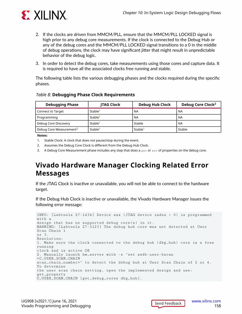
2. If the clocks are driven from MMCM/PLL, ensure that the MMCM/PLL LOCKED signal ishigh prior to any debug core measurements. If the clock is connected to the Debug Hub orany of the debug cores and the MMCM/PLL LOCKED signal transitions to a 0 in the middleof debug operations, the clock may have significant jitter that might result in unpredictablebehavior of the debug logic.
3. In order to detect the debug cores, take measurements using those cores and capture data. Itis required to have all the associated clocks free running and stable.
The following table lists the various debugging phases and the clocks required during the specificphases.
Table 8: Debugging Phase Clock Requirements
Debugging Phase JTAG Clock Debug Hub Clock Debug Core Clock2
Connect to Target Stable1 NA NA
Programming Stable1 NA NA
Debug Core Discovery Stable1 Stable NA
Debug Core Measurement3 Stable1 Stable1 Stable
Notes:1. Stable Clock: A clock that does not pause/stop during the event.2. Assumes the Debug Core Clock is different from the Debug Hub Clock.3. A Debug Core Measurement phase includes any step that does a get or set of properties on the debug core.
Vivado Hardware Manager Clocking Related ErrorMessagesIf the JTAG Clock is inactive or unavailable, you will not be able to connect to the hardwaretarget.
If the Debug Hub Clock is inactive or unavailable, the Vivado Hardware Manager issues thefollowing error message:
INFO: [Labtools 27-1434] Device xxx (JTAG device index = 0) is programmed with a design that has no supported debug core(s) in it.WARNING: [Labtools 27-3123] The debug hub core was not detected at User Scan Chain 1 or 3. Resolution:1. Make sure the clock connected to the debug hub (dbg_hub) core is a free running clock and is active OR2. Manually launch hw_server with -e "set xsdb-user-bscan <C_USER_SCAN_CHAIN scan_chain_number>" to detect the debug hub at User Scan Chain of 2 or 4. To determine the user scan chain setting, open the implemented design and use: get_property C_USER_SCAN_CHAIN [get_debug_cores dbg_hub].
Chapter 10: In-System Logic Design Debugging Flows
UG908 (v2021.1) June 16, 2021 www.xilinx.comVivado Programming and Debugging 158Send Feedback
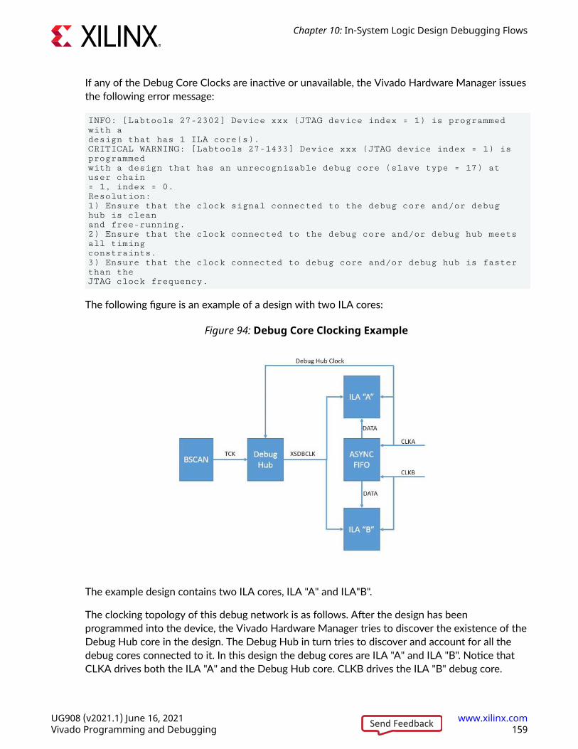
If any of the Debug Core Clocks are inactive or unavailable, the Vivado Hardware Manager issuesthe following error message:
INFO: [Labtools 27-2302] Device xxx (JTAG device index = 1) is programmed with a design that has 1 ILA core(s).CRITICAL WARNING: [Labtools 27-1433] Device xxx (JTAG device index = 1) is programmed with a design that has an unrecognizable debug core (slave type = 17) at user chain = 1, index = 0.Resolution: 1) Ensure that the clock signal connected to the debug core and/or debug hub is clean and free-running.2) Ensure that the clock connected to the debug core and/or debug hub meets all timing constraints.3) Ensure that the clock connected to debug core and/or debug hub is faster than the JTAG clock frequency.
The following figure is an example of a design with two ILA cores:
Figure 94: Debug Core Clocking Example
The example design contains two ILA cores, ILA "A" and ILA"B".
The clocking topology of this debug network is as follows. After the design has beenprogrammed into the device, the Vivado Hardware Manager tries to discover the existence of theDebug Hub core in the design. The Debug Hub in turn tries to discover and account for all thedebug cores connected to it. In this design the debug cores are ILA "A" and ILA "B". Notice thatCLKA drives both the ILA "A" and the Debug Hub core. CLKB drives the ILA "B" debug core.
Chapter 10: In-System Logic Design Debugging Flows
UG908 (v2021.1) June 16, 2021 www.xilinx.comVivado Programming and Debugging 159Send Feedback
When you connect to the target and program the device, we expect an active JTAG clk. In theDebug Core Discovery Phase, we expect a free running and stable clock driving the Debug Hubcore, which in this case is CLKA. During Debug Core Measurement phase (i.e. anything thatinvolves getting/setting properties on the debug core), we expect an active JTAG, Debug Huband Debug Core clocks. If we expect to trigger and capture data on ILA "B", we expect freerunning and stable JTAG, Debug Hub (CLKA), and Debug Core (CLKB) Clocks.
Debug Hub Insertion GuidelinesIn some cases, a design might contain an instance of the Debug Bridge IP that appears to preventthe debug flow from successfully inserting a debug hub and the following error might appear:
[Chipscope 16-336] Failed to find or create hub core for debug slave <debug core name>. Insertion of debug hub is not supported when there are instantiated debug bridge cores in either master mode or switch enabled in the design. Either remove debug slave core or instantiate a debug bridge master in the region of the debug slave
This issue occurs because the debug flow detects the presence of a Debug Bridge IP and doesnot attempt to automatically insert a Debug Hub IP. However, the instance of the Debug BridgeIP in the design is not in the correct mode to connect to a debug core. To resolve this issue,ensure that the design has at least one instance of a Debug Bridge IP in BSCAN-to-Debug Hubmode.
Adding Vivado Debug Cores to a DynamicFunction eXchange Design
Vivado Debug cores can be instantiated in a Dynamic Function eXchange design including withinthe Reconfigurable Modules. There are specific requirements and a methodology to adding andconnecting these cores. See this link in the Vivado Design Suite User Guide: Dynamic FunctioneXchange (UG909) for the methodology needed to add and connect these Vivado Debug cores.
For an example of instantiating debug cores in a Dynamic Function eXchange design as well as adescription of the functionality within the Vivado Hardware Manager, see this link in VivadoDesign Suite Tutorial: Dynamic Function eXchange (UG947).
Chapter 10: In-System Logic Design Debugging Flows
UG908 (v2021.1) June 16, 2021 www.xilinx.comVivado Programming and Debugging 160Send Feedback

Chapter 11
Debugging Logic Designs inHardware
Once you have the debug cores in your design, you can use the run time logic analyzer featuresto debug the design in hardware.
Using Vivado Logic Analyzer to Debug theDesign
The Vivado® logic analyzer feature is used to interact with new ILA, VIO, and JTAG-to-AXIMaster debug cores that are in your design. To access the Vivado logic analyzer feature, click theOpen Hardware Manager button in the Program and Debug section of the Flow Navigator.
The steps to debug your design in hardware using an ILA debug core are:
1. Connect to the hardware target and program the FPGA or ACAP with the .pdi file.
2. Set up the ILA debug core trigger and capture controls.
3. Arm the ILA debug core trigger.
4. View the captured data from the ILA debug core in the Waveform window.
5. Use the VIO debug core to drive control signals and/or view design status signals.
6. Use the JTAG-to-AXI Master debug core to run transactions to interact with various AXIslave cores in your design.
Chapter 11: Debugging Logic Designs in Hardware
UG908 (v2021.1) June 16, 2021 www.xilinx.comVivado Programming and Debugging 161Send Feedback
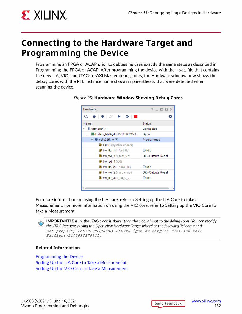
Connecting to the Hardware Target andProgramming the Device
Programming an FPGA or ACAP prior to debugging uses exactly the same steps as described inProgramming the FPGA or ACAP. After programming the device with the .pdi file that containsthe new ILA, VIO, and JTAG-to-AXI Master debug cores, the Hardware window now shows thedebug cores with the RTL instance name shown in parenthesis, that were detected whenscanning the device.
Figure 95: Hardware Window Showing Debug Cores
For more information on using the ILA core, refer to Setting up the ILA Core to take aMeasurement. For more information on using the VIO core, refer to Setting up the VIO Core totake a Measurement.
IMPORTANT! Ensure the JTAG clock is slower than the clocks input to the debug cores. You can modifythe JTAG frequency using the Open New Hardware Target wizard or the following Tcl command:set_property PARAM.FREQUENCY 250000 [get_hw_targets */xilinx_tcf/Digilent/210203327962A]
Related Information
Programming the DeviceSetting Up the ILA Core to Take a MeasurementSetting Up the VIO Core to Take a Measurement
Chapter 11: Debugging Logic Designs in Hardware
UG908 (v2021.1) June 16, 2021 www.xilinx.comVivado Programming and Debugging 162Send Feedback
Vivado Hardware Manager DashboardsThe Vivado Hardware Manager Dashboards help you manage the various windows for yourSystem Monitor, ILA, and VIO Debug cores. The dashboards enable you to create, modify, andsave the configuration of these windows in your Vivado Design Suite project.
Default DashboardsWhen debug cores are detected upon refreshing a hardware device, the default dashboard foreach debug core is automatically opened.
Default Dashboard WindowsEvery default dashboard contains windows relevant to the debug core the dashboard is createdfor. The default dashboard created for the ILA debug core contains five windows:
• Settings window
• Status window
• Trigger Setup window
• Capture Setup window
• Waveform window
An example of the default ILA Dashboard can be seen below.
Chapter 11: Debugging Logic Designs in Hardware
UG908 (v2021.1) June 16, 2021 www.xilinx.comVivado Programming and Debugging 163Send Feedback
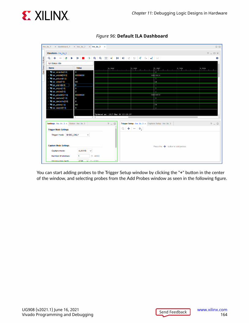
Figure 96: Default ILA Dashboard
You can start adding probes to the Trigger Setup window by clicking the "+" button in the centerof the window, and selecting probes from the Add Probes window as seen in the following figure.
Chapter 11: Debugging Logic Designs in Hardware
UG908 (v2021.1) June 16, 2021 www.xilinx.comVivado Programming and Debugging 164Send Feedback
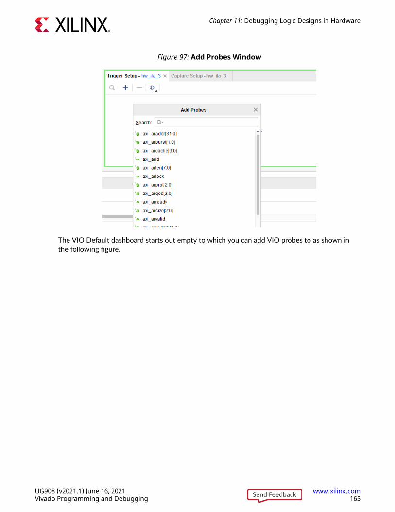
Figure 97: Add Probes Window
The VIO Default dashboard starts out empty to which you can add VIO probes to as shown inthe following figure.
Chapter 11: Debugging Logic Designs in Hardware
UG908 (v2021.1) June 16, 2021 www.xilinx.comVivado Programming and Debugging 165Send Feedback
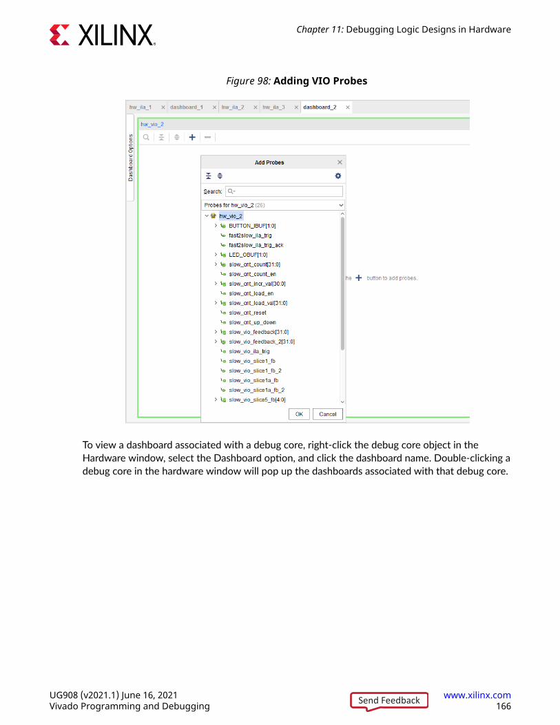
Figure 98: Adding VIO Probes
To view a dashboard associated with a debug core, right-click the debug core object in theHardware window, select the Dashboard option, and click the dashboard name. Double-clicking adebug core in the hardware window will pop up the dashboards associated with that debug core.
Chapter 11: Debugging Logic Designs in Hardware
UG908 (v2021.1) June 16, 2021 www.xilinx.comVivado Programming and Debugging 166Send Feedback
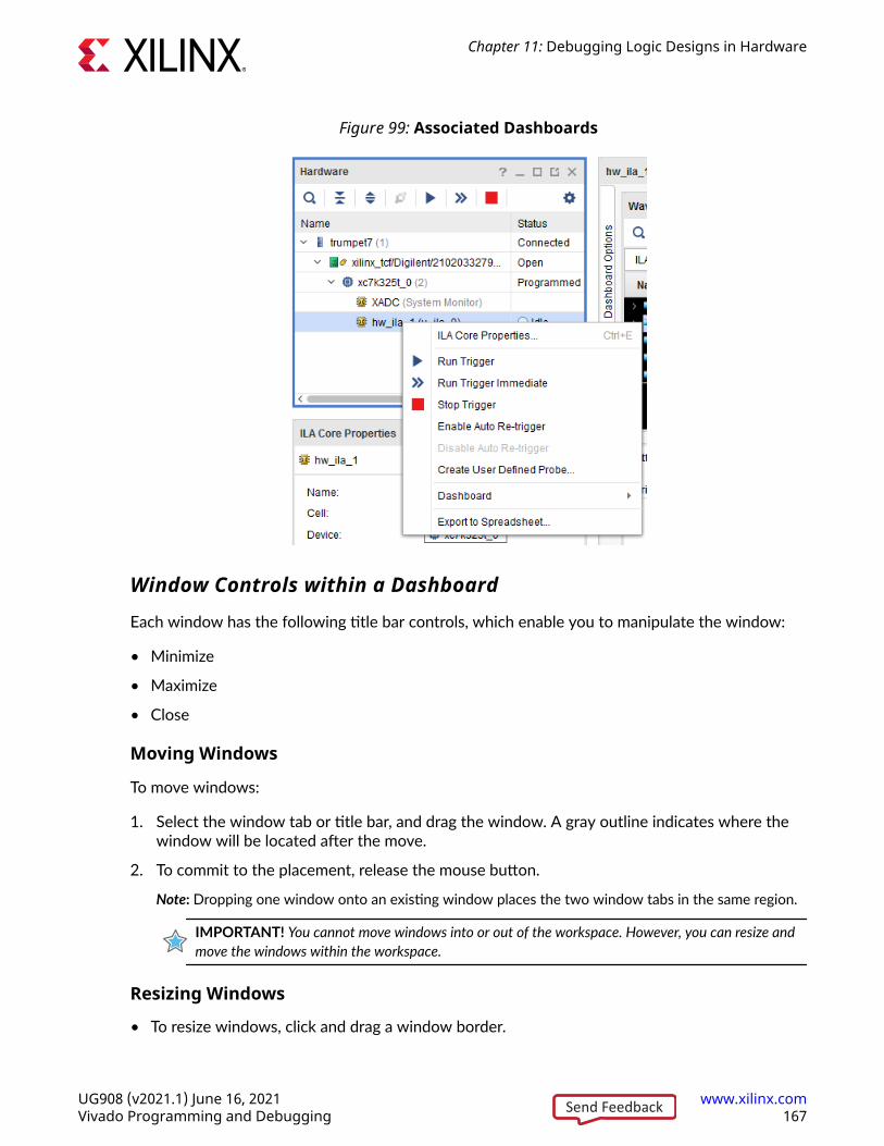
Figure 99: Associated Dashboards
Window Controls within a Dashboard
Each window has the following title bar controls, which enable you to manipulate the window:
• Minimize
• Maximize
• Close
Moving Windows
To move windows:
1. Select the window tab or title bar, and drag the window. A gray outline indicates where thewindow will be located after the move.
2. To commit to the placement, release the mouse button.
Note: Dropping one window onto an existing window places the two window tabs in the same region.
IMPORTANT! You cannot move windows into or out of the workspace. However, you can resize andmove the windows within the workspace.
Resizing Windows
• To resize windows, click and drag a window border.
Chapter 11: Debugging Logic Designs in Hardware
UG908 (v2021.1) June 16, 2021 www.xilinx.comVivado Programming and Debugging 167Send Feedback
Note: The mouse cursor changes to a resize cursor when positioned over a window border or draghandle, indicating that you can click and drag the window border to resize the window.
• To expand a window to use the all of the viewing environment, click the Maximize button inthe upper right corner of the window.
• To restore a window to its original size, double-click the window title bar or tab.
Closing Windows
• To close windows, click the Close button in the upper right corner of the window.
Note: In some cases, this button is also available in the window tab.
• Right-click a window tab or title bar, and select Close from the popup menu.
Window Tabs
Each window has a tab that you can select to make that the window is active. The tab is at thebottom of some windows, such as the Trigger Setup and Capture Setup windows.
TIP: To make the next tab active, press Ctrl+Tab. To make the previous tab active, press Ctrl+Shift+Tab. Tomaximize or minimize the window, double-click the window tab.
Customizing DashboardsTypically the windows in the default dashboards should be enough to debug your design andview the results. However there are times when you might want to move windows around (i.e.customize your dashboards). For example you may want to be able to view both the ILA statusand Waveform window in addition to controlling VIO probes in the same dashboard. In thosesituations Xilinx recommends customizing the dashboard to fit your needs.
Dashboard Options
Every dashboard has a Dashboard Options slideout on the left. Use the Dashboard Optionsbutton on the left side of a dashboard to open its Dashboard Options settings. The DashboardOptions settings allow you to control the windows that appear in a specific dashboard. Forexample you may want to customize the ILA dashboard to include one of the VIO windows aswell. As shown below you click on the VIO window to include it in the Dashboard Options andthe VIO window shows up in the ILA Dashboard. You can now add the VIO probes you areinterested in and trigger the ILA window.
Chapter 11: Debugging Logic Designs in Hardware
UG908 (v2021.1) June 16, 2021 www.xilinx.comVivado Programming and Debugging 168Send Feedback
Figure 100: Adding Dashboard Options
Click the Dashboard Options button on the left side of a dashboard to open and close theDashboard Options slideout.
Creating New Dashboards
In addition to customizing Default Dashboards using the Dashboard Options, you can also createbrand new dashboards. To do that right-click the debug core object in the Hardware window andselect the Dashboard → New Dashboard option as shown in the following figure.
Chapter 11: Debugging Logic Designs in Hardware
UG908 (v2021.1) June 16, 2021 www.xilinx.comVivado Programming and Debugging 169Send Feedback
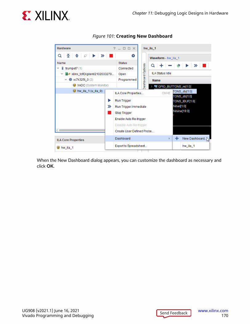
Figure 101: Creating New Dashboard
When the New Dashboard dialog appears, you can customize the dashboard as necessary andclick OK.
Chapter 11: Debugging Logic Designs in Hardware
UG908 (v2021.1) June 16, 2021 www.xilinx.comVivado Programming and Debugging 170Send Feedback
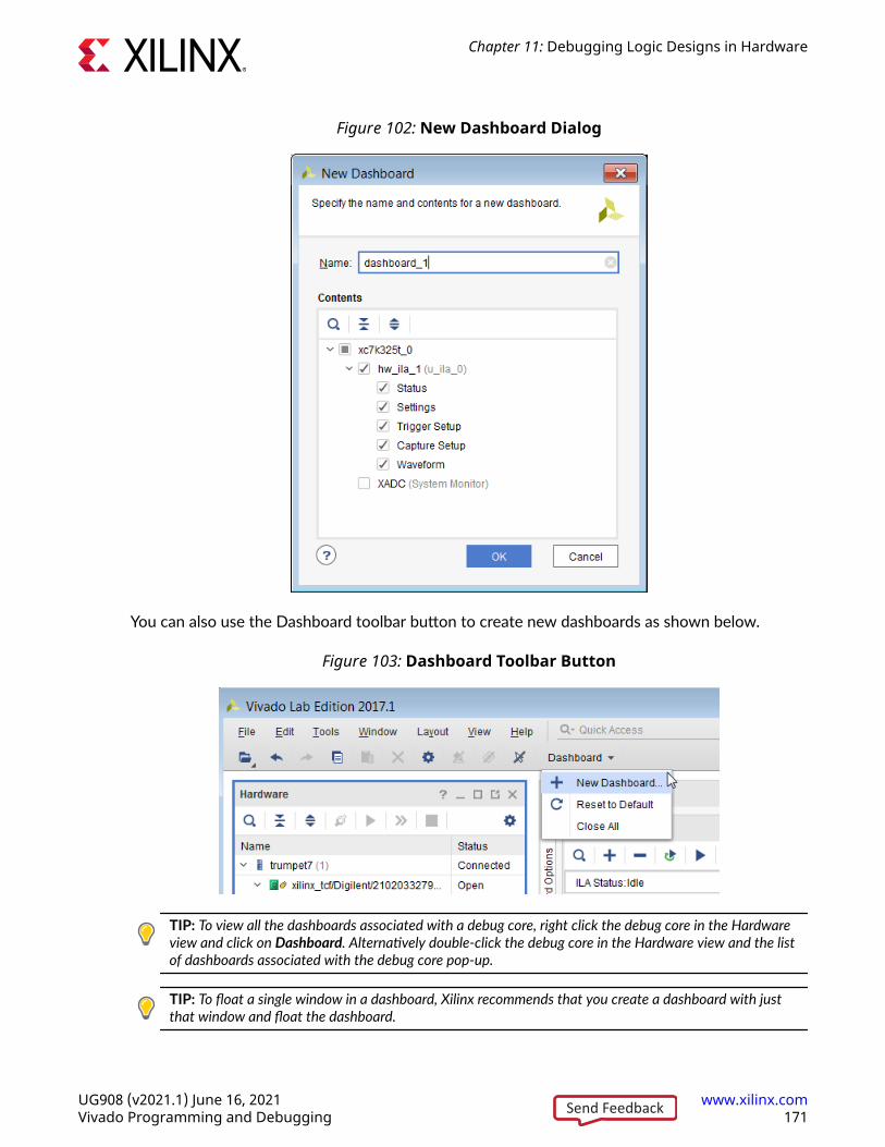
Figure 102: New Dashboard Dialog
You can also use the Dashboard toolbar button to create new dashboards as shown below.
Figure 103: Dashboard Toolbar Button
TIP: To view all the dashboards associated with a debug core, right click the debug core in the Hardwareview and click on Dashboard. Alternatively double-click the debug core in the Hardware view and the listof dashboards associated with the debug core pop-up.
TIP: To float a single window in a dashboard, Xilinx recommends that you create a dashboard with justthat window and float the dashboard.
Chapter 11: Debugging Logic Designs in Hardware
UG908 (v2021.1) June 16, 2021 www.xilinx.comVivado Programming and Debugging 171Send Feedback
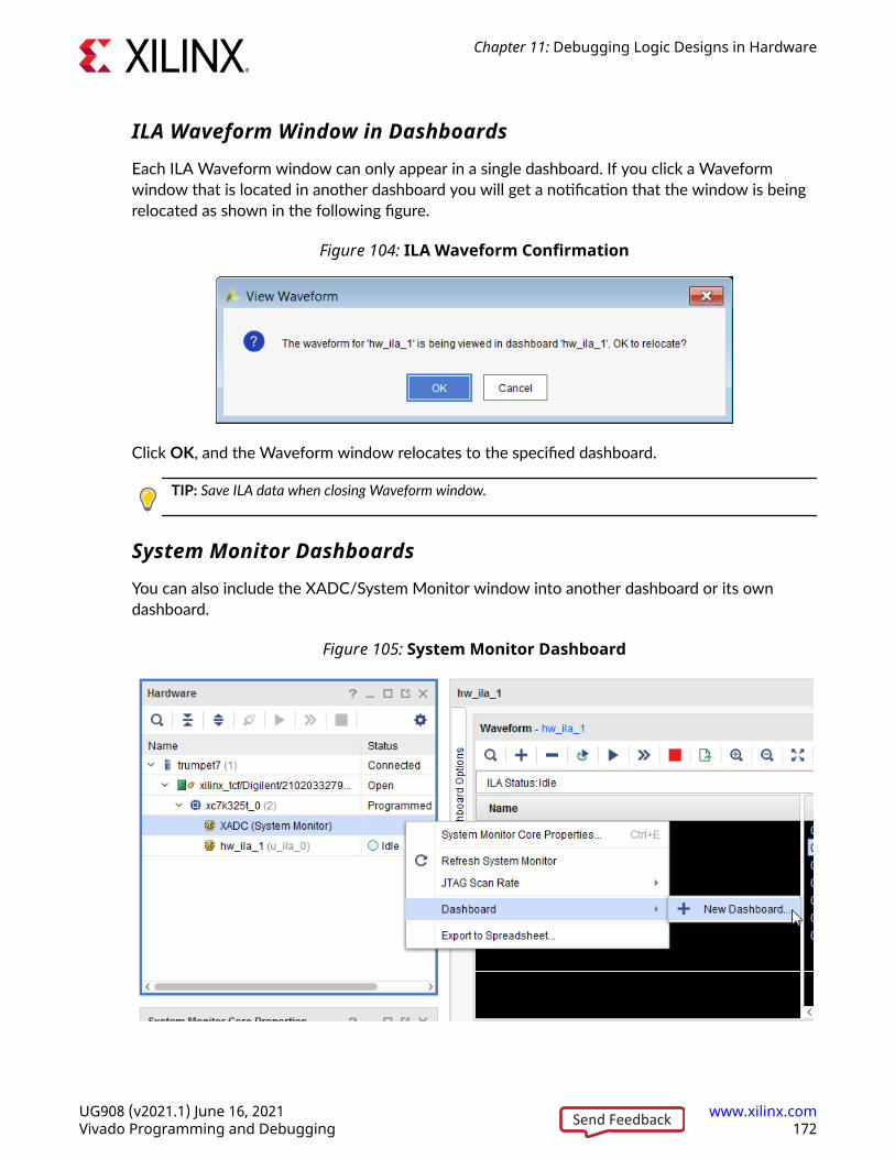
ILA Waveform Window in Dashboards
Each ILA Waveform window can only appear in a single dashboard. If you click a Waveformwindow that is located in another dashboard you will get a notification that the window is beingrelocated as shown in the following figure.
Figure 104: ILA Waveform Confirmation
Click OK, and the Waveform window relocates to the specified dashboard.
TIP: Save ILA data when closing Waveform window.
System Monitor Dashboards
You can also include the XADC/System Monitor window into another dashboard or its owndashboard.
Figure 105: System Monitor Dashboard
Chapter 11: Debugging Logic Designs in Hardware
UG908 (v2021.1) June 16, 2021 www.xilinx.comVivado Programming and Debugging 172Send Feedback
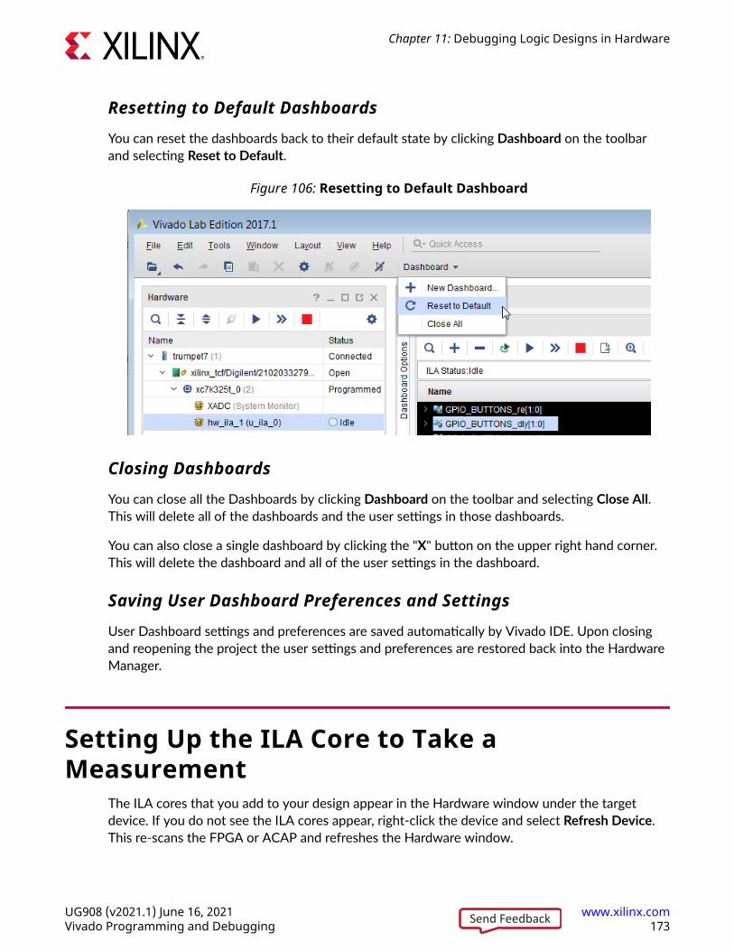
Resetting to Default Dashboards
You can reset the dashboards back to their default state by clicking Dashboard on the toolbarand selecting Reset to Default.
Figure 106: Resetting to Default Dashboard
Closing Dashboards
You can close all the Dashboards by clicking Dashboard on the toolbar and selecting Close All.This will delete all of the dashboards and the user settings in those dashboards.
You can also close a single dashboard by clicking the "X" button on the upper right hand corner.This will delete the dashboard and all of the user settings in the dashboard.
Saving User Dashboard Preferences and Settings
User Dashboard settings and preferences are saved automatically by Vivado IDE. Upon closingand reopening the project the user settings and preferences are restored back into the HardwareManager.
Setting Up the ILA Core to Take aMeasurement
The ILA cores that you add to your design appear in the Hardware window under the targetdevice. If you do not see the ILA cores appear, right-click the device and select Refresh Device.This re-scans the FPGA or ACAP and refreshes the Hardware window.
Chapter 11: Debugging Logic Designs in Hardware
UG908 (v2021.1) June 16, 2021 www.xilinx.comVivado Programming and Debugging 173Send Feedback
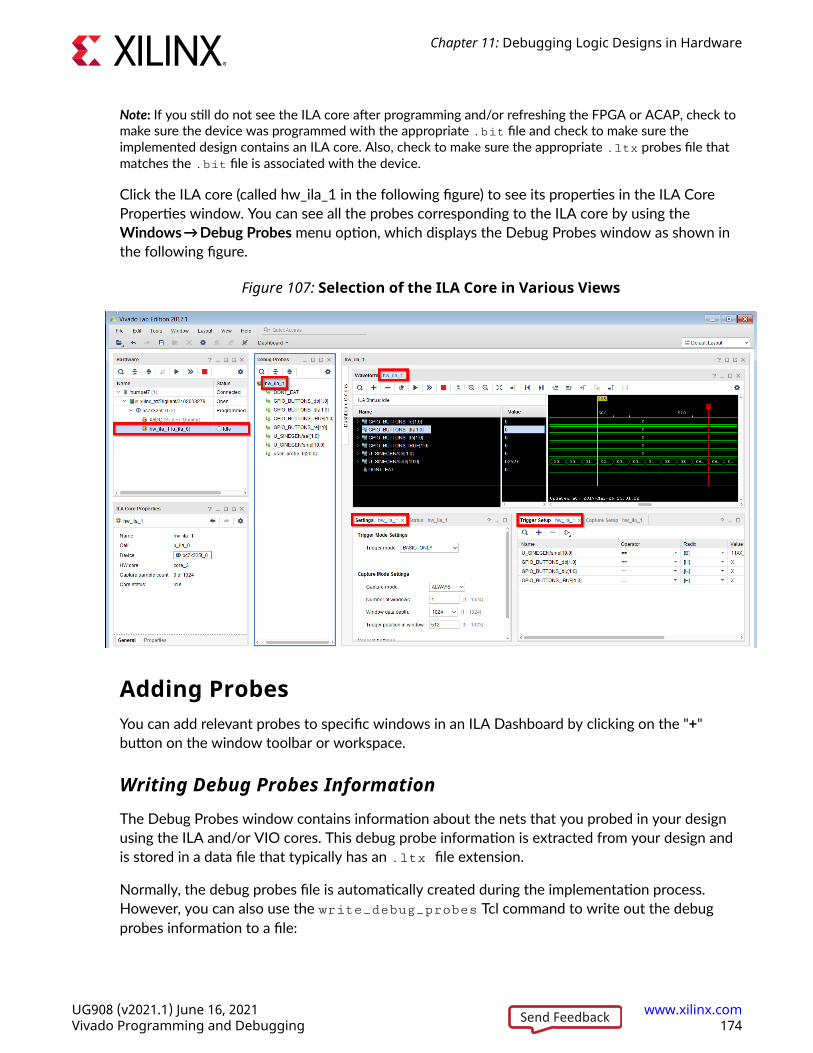
Note: If you still do not see the ILA core after programming and/or refreshing the FPGA or ACAP, check tomake sure the device was programmed with the appropriate .bit file and check to make sure theimplemented design contains an ILA core. Also, check to make sure the appropriate .ltx probes file thatmatches the .bit file is associated with the device.
Click the ILA core (called hw_ila_1 in the following figure) to see its properties in the ILA CoreProperties window. You can see all the probes corresponding to the ILA core by using theWindows → Debug Probes menu option, which displays the Debug Probes window as shown inthe following figure.
Figure 107: Selection of the ILA Core in Various Views
Adding ProbesYou can add relevant probes to specific windows in an ILA Dashboard by clicking on the "+"button on the window toolbar or workspace.
Writing Debug Probes Information
The Debug Probes window contains information about the nets that you probed in your designusing the ILA and/or VIO cores. This debug probe information is extracted from your design andis stored in a data file that typically has an .ltx file extension.
Normally, the debug probes file is automatically created during the implementation process.However, you can also use the write_debug_probes Tcl command to write out the debugprobes information to a file:
Chapter 11: Debugging Logic Designs in Hardware
UG908 (v2021.1) June 16, 2021 www.xilinx.comVivado Programming and Debugging 174Send Feedback
1. Open the Synthesized or Netlist Design.
2. Run the write_debug_probes filename.ltx Tcl command.
IMPORTANT! If you are using non-project mode, you must manually call thewrite_debug_probes command immediately following the opt_design command.
Reading Debug Probes Information
The debug probes file is automatically associated with the hardware device if the Vivado IDE is inproject mode and a probes file is called debug_nets.ltx is found in the same directory as thebitstream programming (.bit) file that is associated with the device.
You can also specify the location of the probes file:
1. Select the hardware device in the Hardware window.
2. Set the Probes file location in the Hardware Device Properties window.
3. Right-click the hardware device in the Hardware window and select Refresh Device to readthe contents of the debug probes file and associate and validate the information with thedebug cores found in the design running in the hardware device.
You can also set the location using the following Tcl commands to associate a debug probes filecalled C:\myprobes.ltx with the first device on the target board:
% set_property PROBES.FILE {C:/myprobes.ltx} [lindex [get_hw_devices] 0]% refresh_hw_device [lindex [get_hw_devices] 0]
Renaming Debug Probes
You can use the Debug Probes window to rename debug probes that belong to an ILA or VIOcore. You can rename the debug probes and add them to an existing Waveform Viewer for thecore, or you can add them to the various trigger and/or capture windows of the ILA Dashboard.These names could be the custom, long or short name associated with the debug probe.
To perform these operations, right-click an ILA/VIO core's debug probe(s) and select one of thefollowing:
• Rename: Prompts you to rename the probe to a custom name.
• Name: Allows you to select the long, short, or custom name of the debug probe. Subsequentreferences to the debug probe in the Vivado IDE window will use the name that you selected.
• Long: Displays the full hierarchical name of the signal or bus being probed.
• Short: Displays the name of the signal or bus being probed.
• Custom: Displays the custom name given to the signal or bus when renamed.
Chapter 11: Debugging Logic Designs in Hardware
UG908 (v2021.1) June 16, 2021 www.xilinx.comVivado Programming and Debugging 175Send Feedback
Using Multiple ComparatorsIf you have customized the probes and/or ILA debug cores to use more than 1 comparator in theBasic/Advanced mode, you can use these comparators both in the Basic and Advanced TriggerSetup window.
You can add the probe into the Basic trigger setup window and set up the trigger conditions. Thecomparator usage column gives you information on the comparator used within the probe for thespecific compare condition out of the total number of comparators associated with the probe.
Figure 108: Basic Trigger Setup - Comparator Usage
TIP: The Comparator Usage column is a hidden column. To enable this column right-click the Trigger Setupcolumn title row as shown below and select Comparator Usage.
Chapter 11: Debugging Logic Designs in Hardware
UG908 (v2021.1) June 16, 2021 www.xilinx.comVivado Programming and Debugging 176Send Feedback
Figure 109: Comparator Usage Column
Using the ILA Default DashboardThe ILA Dashboard (see the following figure) is a central location for all status and controlinformation pertaining to a given ILA core. When an ILA core is first detected upon refreshing ahardware device, the Default ILA Dashboard for the core is automatically opened. If you need tomanually open or re-open the dashboard, just right-click the ILA core object in the Hardwarewindow and select Default Dashboard.
Figure 110: ILA Dashboard
Chapter 11: Debugging Logic Designs in Hardware
UG908 (v2021.1) June 16, 2021 www.xilinx.comVivado Programming and Debugging 177Send Feedback
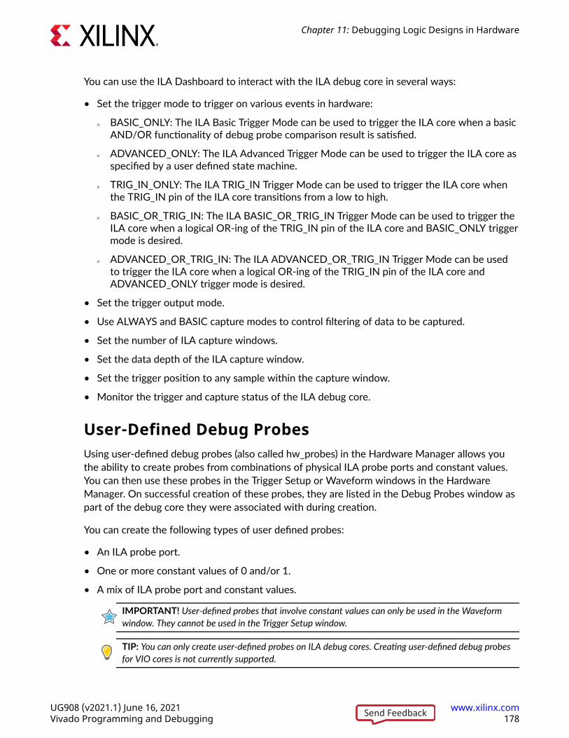
You can use the ILA Dashboard to interact with the ILA debug core in several ways:
• Set the trigger mode to trigger on various events in hardware:
○ BASIC_ONLY: The ILA Basic Trigger Mode can be used to trigger the ILA core when a basicAND/OR functionality of debug probe comparison result is satisfied.
○ ADVANCED_ONLY: The ILA Advanced Trigger Mode can be used to trigger the ILA core asspecified by a user defined state machine.
○ TRIG_IN_ONLY: The ILA TRIG_IN Trigger Mode can be used to trigger the ILA core whenthe TRIG_IN pin of the ILA core transitions from a low to high.
○ BASIC_OR_TRIG_IN: The ILA BASIC_OR_TRIG_IN Trigger Mode can be used to trigger theILA core when a logical OR-ing of the TRIG_IN pin of the ILA core and BASIC_ONLY triggermode is desired.
○ ADVANCED_OR_TRIG_IN: The ILA ADVANCED_OR_TRIG_IN Trigger Mode can be usedto trigger the ILA core when a logical OR-ing of the TRIG_IN pin of the ILA core andADVANCED_ONLY trigger mode is desired.
• Set the trigger output mode.
• Use ALWAYS and BASIC capture modes to control filtering of data to be captured.
• Set the number of ILA capture windows.
• Set the data depth of the ILA capture window.
• Set the trigger position to any sample within the capture window.
• Monitor the trigger and capture status of the ILA debug core.
User-Defined Debug ProbesUsing user-defined debug probes (also called hw_probes) in the Hardware Manager allows youthe ability to create probes from combinations of physical ILA probe ports and constant values.You can then use these probes in the Trigger Setup or Waveform windows in the HardwareManager. On successful creation of these probes, they are listed in the Debug Probes window aspart of the debug core they were associated with during creation.
You can create the following types of user defined probes:
• An ILA probe port.
• One or more constant values of 0 and/or 1.
• A mix of ILA probe port and constant values.
IMPORTANT! User-defined probes that involve constant values can only be used in the Waveformwindow. They cannot be used in the Trigger Setup window.
TIP: You can only create user-defined probes on ILA debug cores. Creating user-defined debug probesfor VIO cores is not currently supported.
Chapter 11: Debugging Logic Designs in Hardware
UG908 (v2021.1) June 16, 2021 www.xilinx.comVivado Programming and Debugging 178Send Feedback
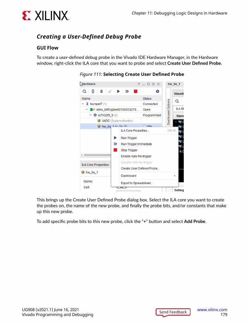
Creating a User-Defined Debug Probe
GUI Flow
To create a user-defined debug probe in the Vivado IDE Hardware Manager, in the Hardwarewindow, right-click the ILA core that you want to probe and select Create User Defined Probe.
Figure 111: Selecting Create User Defined Probe
This brings up the Create User Defined Probe dialog box. Select the ILA core you want to createthe probes on, the name of the new probe, and finally the probe bits, and/or constants that makeup this new probe.
To add specific probe bits to this new probe, click the "+" button and select Add Probe.
Chapter 11: Debugging Logic Designs in Hardware
UG908 (v2021.1) June 16, 2021 www.xilinx.comVivado Programming and Debugging 179Send Feedback
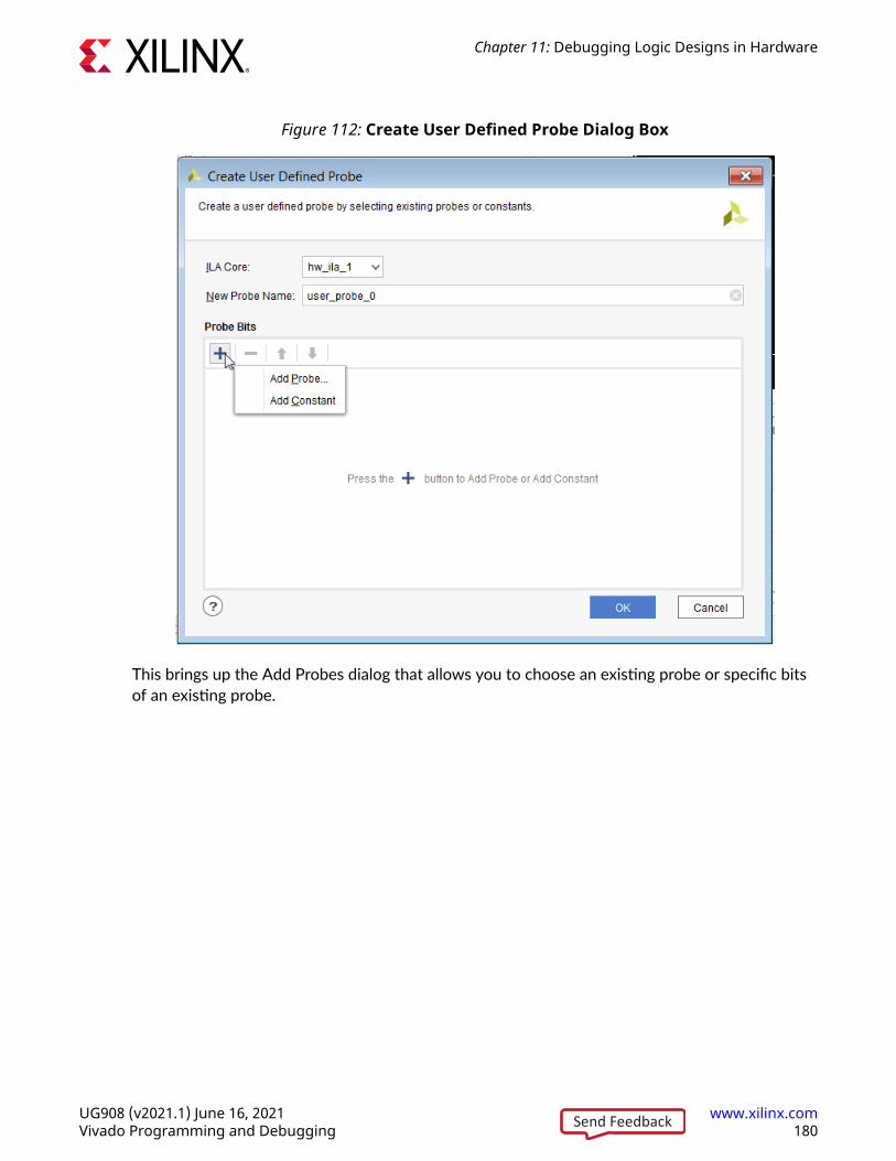
Figure 112: Create User Defined Probe Dialog Box
This brings up the Add Probes dialog that allows you to choose an existing probe or specific bitsof an existing probe.
Chapter 11: Debugging Logic Designs in Hardware
UG908 (v2021.1) June 16, 2021 www.xilinx.comVivado Programming and Debugging 180Send Feedback
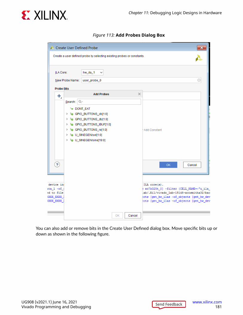
Figure 113: Add Probes Dialog Box
You can also add or remove bits in the Create User Defined dialog box. Move specific bits up ordown as shown in the following figure.
Chapter 11: Debugging Logic Designs in Hardware
UG908 (v2021.1) June 16, 2021 www.xilinx.comVivado Programming and Debugging 181Send Feedback
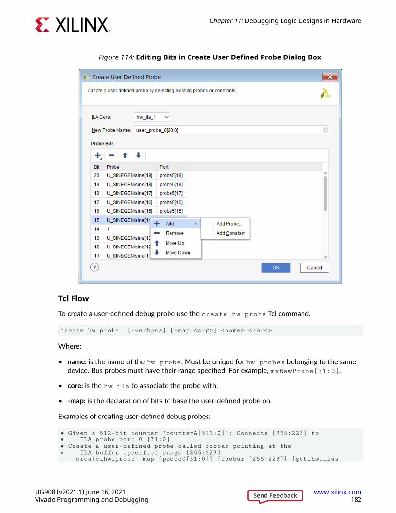
Figure 114: Editing Bits in Create User Defined Probe Dialog Box
Tcl Flow
To create a user-defined debug probe use the create_hw_probe Tcl command.
create_hw_probe [-verbose] [-map <arg>] <name> <core>
Where:
• name: is the name of the hw_probe. Must be unique for hw_probes belonging to the samedevice. Bus probes must have their range specified. For example, myNewProbe[31:0].
• core: is the hw_ila to associate the probe with.
• -map: is the declaration of bits to base the user-defined probe on.
Examples of creating user-defined debug probes:
# Given a 512-bit counter "counterA[511:0]": Connects [255:223] to # ILA probe port 0 [31:0]# Create a user-defined probe called foobar pointing at the # ILA buffer specified range [255:223] create_hw_probe -map {probe0[31:0]} {foobar [255:223]} [get_hw_ilas
Chapter 11: Debugging Logic Designs in Hardware
UG908 (v2021.1) June 16, 2021 www.xilinx.comVivado Programming and Debugging 182Send Feedback
hw_ila_1]# Constant only probe. NO triggering allowed on constant ONLY probes. create_hw_probe -map {0} {my_constant_gnd[0:0]} [get_hw_ilas hw_ila_1]# Create a user-defined probe as a mix of constants and ILA probe ports create_hw_probe -map {0000 probe0[31:0] 1010} {my_mixed_probe[47:8]} [get_hw_ilas hw_ila_1] # Creating scalar hw_probe called "foobar" from probe1:create_hw_probe -map {probe1} foobar [get_hw_ilas hw_ila_1]# Creating scalar hw_probe called "foobar" from bit 3 of probe0:create_hw_probe -map {probe0[3]} foobar [get_hw_ilas hw_ila_1]# Creating vector hw_probe called "foobar[0:0]" from probe1:create_hw_probe -map {probe1} foobar[0:0] [get_hw_ilas hw_ila_1]# Creating vector probe called "foobar[3:0]" from probe0:create_hw_probe -map {probe0} foobar[3:0] [get_hw_ilas hw_ila_1]# Creating vector probe called "foobar[3:2]" from probe0[1:0]:create_hw_probe -map {probe0[1:0]} foobar[3:2] [get_hw_ilas hw_ila_1]
Deleting a User-Defined Debug Probe
GUI Flow
To delete a user defined probe in the Vivado IDE Hardware Manager, select Window → DebugProbe. This will bring up the Debug Probes window beside the Hardware Manager dashboards.Right-click the appropriate probe in this window and click Delete as shown below.
Chapter 11: Debugging Logic Designs in Hardware
UG908 (v2021.1) June 16, 2021 www.xilinx.comVivado Programming and Debugging 183Send Feedback
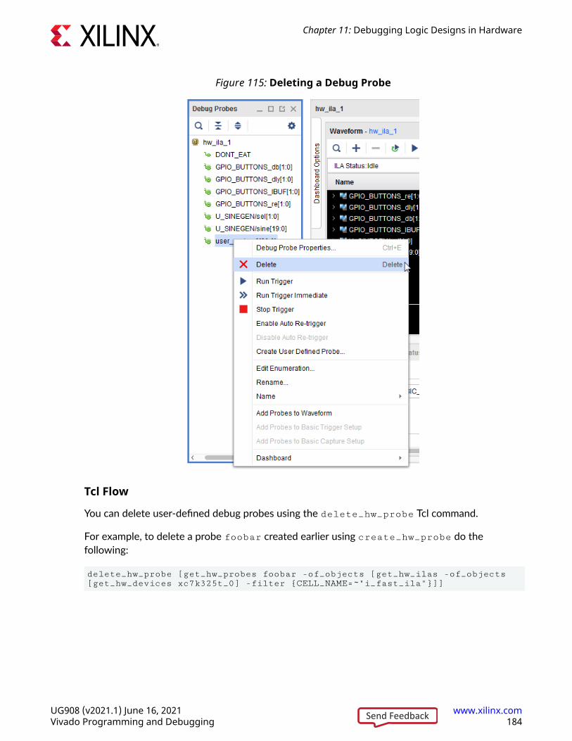
Figure 115: Deleting a Debug Probe
Tcl Flow
You can delete user-defined debug probes using the delete_hw_probe Tcl command.
For example, to delete a probe foobar created earlier using create_hw_probe do thefollowing:
delete_hw_probe [get_hw_probes foobar -of_objects [get_hw_ilas -of_objects [get_hw_devices xc7k325t_0] -filter {CELL_NAME=~"i_fast_ila"}]]
Chapter 11: Debugging Logic Designs in Hardware
UG908 (v2021.1) June 16, 2021 www.xilinx.comVivado Programming and Debugging 184Send Feedback
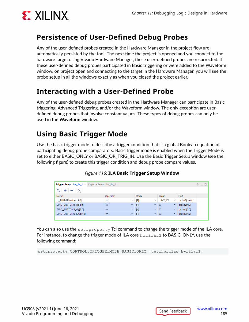
Persistence of User-Defined Debug ProbesAny of the user-defined probes created in the Hardware Manager in the project flow areautomatically persisted by the tool. The next time the project is opened and you connect to thehardware target using Vivado Hardware Manager, these user-defined probes are resurrected. Ifthese user-defined debug probes participated in Basic triggering or were added to the Waveformwindow, on project open and connecting to the target in the Hardware Manager, you will see theprobe setup in all the windows exactly as when you closed the project earlier.
Interacting with a User-Defined ProbeAny of the user-defined debug probes created in the Hardware Manager can participate in Basictriggering, Advanced Triggering, and/or the Waveform window. The only exception are user-defined debug probes that involve constant values. These types of debug probes can only beused in the Waveform window.
Using Basic Trigger ModeUse the basic trigger mode to describe a trigger condition that is a global Boolean equation ofparticipating debug probe comparators. Basic trigger mode is enabled when the Trigger Mode isset to either BASIC_ONLY or BASIC_OR_TRIG_IN. Use the Basic Trigger Setup window (see thefollowing figure) to create this trigger condition and debug probe compare values.
Figure 116: ILA Basic Trigger Setup Window
You can also use the set_property Tcl command to change the trigger mode of the ILA core.For instance, to change the trigger mode of ILA core hw_ila_1 to BASIC_ONLY, use thefollowing command:
set_property CONTROL.TRIGGER_MODE BASIC_ONLY [get_hw_ilas hw_ila_1]
Chapter 11: Debugging Logic Designs in Hardware
UG908 (v2021.1) June 16, 2021 www.xilinx.comVivado Programming and Debugging 185Send Feedback
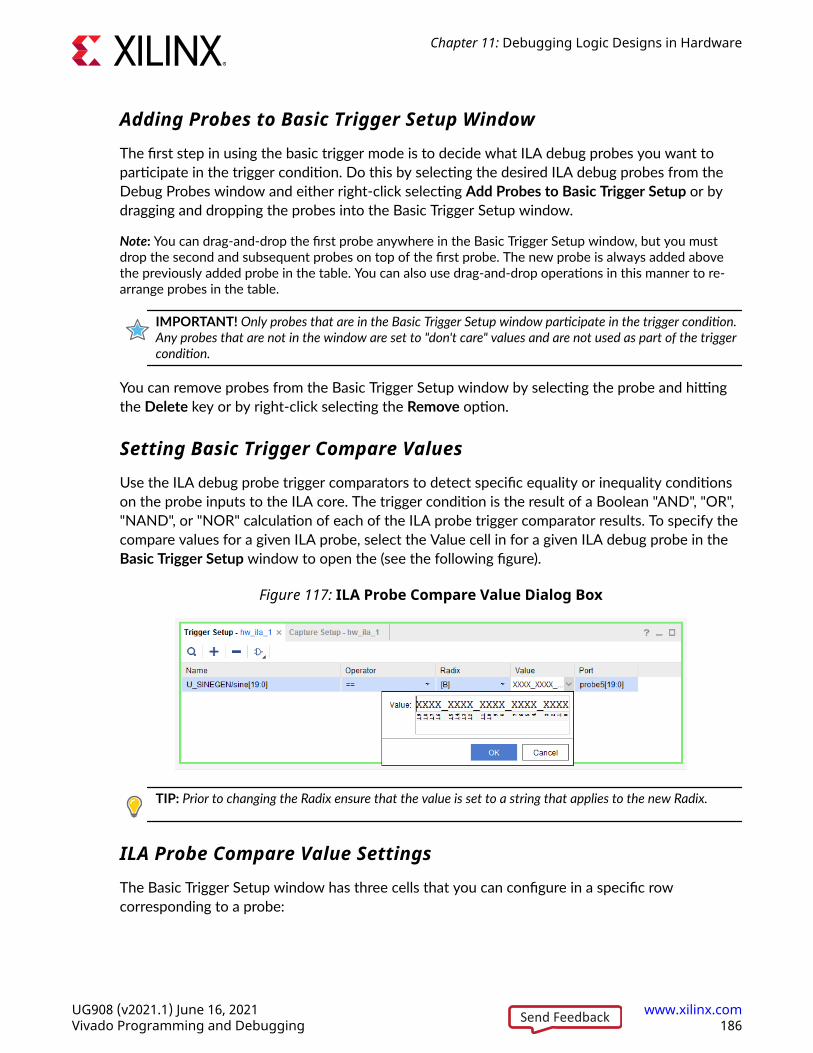
Adding Probes to Basic Trigger Setup Window
The first step in using the basic trigger mode is to decide what ILA debug probes you want toparticipate in the trigger condition. Do this by selecting the desired ILA debug probes from theDebug Probes window and either right-click selecting Add Probes to Basic Trigger Setup or bydragging and dropping the probes into the Basic Trigger Setup window.
Note: You can drag-and-drop the first probe anywhere in the Basic Trigger Setup window, but you mustdrop the second and subsequent probes on top of the first probe. The new probe is always added abovethe previously added probe in the table. You can also use drag-and-drop operations in this manner to re-arrange probes in the table.
IMPORTANT! Only probes that are in the Basic Trigger Setup window participate in the trigger condition.Any probes that are not in the window are set to "don't care" values and are not used as part of the triggercondition.
You can remove probes from the Basic Trigger Setup window by selecting the probe and hittingthe Delete key or by right-click selecting the Remove option.
Setting Basic Trigger Compare Values
Use the ILA debug probe trigger comparators to detect specific equality or inequality conditionson the probe inputs to the ILA core. The trigger condition is the result of a Boolean "AND", "OR","NAND", or "NOR" calculation of each of the ILA probe trigger comparator results. To specify thecompare values for a given ILA probe, select the Value cell in for a given ILA debug probe in theBasic Trigger Setup window to open the (see the following figure).
Figure 117: ILA Probe Compare Value Dialog Box
TIP: Prior to changing the Radix ensure that the value is set to a string that applies to the new Radix.
ILA Probe Compare Value Settings
The Basic Trigger Setup window has three cells that you can configure in a specific rowcorresponding to a probe:
Chapter 11: Debugging Logic Designs in Hardware
UG908 (v2021.1) June 16, 2021 www.xilinx.comVivado Programming and Debugging 186Send Feedback
1. Operator: This is the comparison operator that you can set to the following values:
• == (equal)
• != (not equal)
• < (less than)
• <= (less than or equal)
• > (greater than)
• >= (greater than or equal)
2. Radix: This is the radix or base of the Value that you can set to the following values:
• [B] Binary
• [H] Hexadecimal
• [O] Octal
• [U] Unsigned Decimal
• [S] Signed Decimal
3. Value: This is the comparison value that will be compared (using the Operator) with the real-time value on the net(s) in the design that are connected to the probe input of the ILA debugcore. Depending on the Radix settings, the Value string is as follows:
• Binary
○ 0: logical zero
○ 1: logical one
○ X: don't care
○ R: rising or low-to-high transition
○ F: falling or high-to-low transition
○ B: either low-to-high or high-to-low transitions
○ N: no transition (current sample value is the same as the previous value)
• Hexadecimal
○ X: All bits corresponding to the value string character are "don't care" values
○ 0-9: Values 0 through 9
○ A-F: Values 10 through 15
• Octal
○ X: All bits corresponding to the value string character are "don't care" values
○ 0-7: Values 0 through 7
Chapter 11: Debugging Logic Designs in Hardware
UG908 (v2021.1) June 16, 2021 www.xilinx.comVivado Programming and Debugging 187Send Feedback
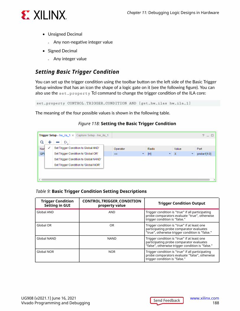
• Unsigned Decimal
○ Any non-negative integer value
• Signed Decimal
○ Any integer value
Setting Basic Trigger Condition
You can set up the trigger condition using the toolbar button on the left side of the Basic TriggerSetup window that has an icon the shape of a logic gate on it (see the following figure). You canalso use the set_property Tcl command to change the trigger condition of the ILA core:
set_property CONTROL.TRIGGER_CONDITION AND [get_hw_ilas hw_ila_1]
The meaning of the four possible values is shown in the following table.
Figure 118: Setting the Basic Trigger Condition
Table 9: Basic Trigger Condition Setting Descriptions
Trigger ConditionSetting in GUI
CONTROL.TRIGGER_CONDITIONproperty value Trigger Condition Output
Global AND AND Trigger condition is "true" if all participatingprobe comparators evaluate “true”, otherwisetrigger condition is “false.”
Global OR OR Trigger condition is "true" if at least oneparticipating probe comparator evaluates"true", otherwise trigger condition is "false."
Global NAND NAND Trigger condition is “true” if at least oneparticipating probe comparator evaluates“false”, otherwise trigger condition is “false.”
Global NOR NOR Trigger condition is "true" if all participatingprobe comparators evaluate "false", otherwisetrigger condition is "false."
Chapter 11: Debugging Logic Designs in Hardware
UG908 (v2021.1) June 16, 2021 www.xilinx.comVivado Programming and Debugging 188Send Feedback
IMPORTANT! If the ILA core has two or more debug probes that concatenated together to share a singlephysical probe port of the ILA core, then only the "Global AND" (AND) and "Global NAND" (NAND) triggercondition settings are supported. The "Global OR" (OR) and "Global NOR" (NOR) functions are notsupported due to limitations of the probe port comparator logic. If you want to use the "Global OR" (OR) or"Global NOR" (NOR) trigger condition settings, then make sure you assign each unique net or bus net toseparate probe ports of the ILA core.
Using Advanced Trigger ModeThe ILA core can be configured at core generation or insertion time to have advanced triggercapabilities that include the following features:
• Trigger state machine consisting of up to 16 states.
• Each state can consist of one-, two-, or three-way conditional branching.
• Up to four counters can be used in a trigger state machine program to keep track of multipleevents.
• Up to four flags can be used in a trigger state machine program to indicate when certainbranches are taken.
• The state machine can execute "goto", "trigger", and various counter- and flag-related actions.
If the ILA core in the design that is running in the hardware device has advanced triggercapabilities, the advanced trigger mode features can be enabled by setting the Trigger modecontrol in the ILA Properties window of the ILA Dashboard to ADVANCED_ONLY orADVANCED_OR_TRIG_IN.
Specifying the Trigger State Machine Program File
When you set the Trigger mode to ADVANCED_ONLY or ADVANCED_OR_TRIG_IN, twochanges happen in the ILA Dashboard:
1. A new control called Trigger State Machine appears in the ILA Properties window
2. The Basic Trigger Setup window is replaced by a Trigger State Machine code editor window.
If you are specifying an ILA trigger state machine program for the first time, the Trigger StateMachine code editor window will appear as the one shown in the following figure.
Chapter 11: Debugging Logic Designs in Hardware
UG908 (v2021.1) June 16, 2021 www.xilinx.comVivado Programming and Debugging 189Send Feedback
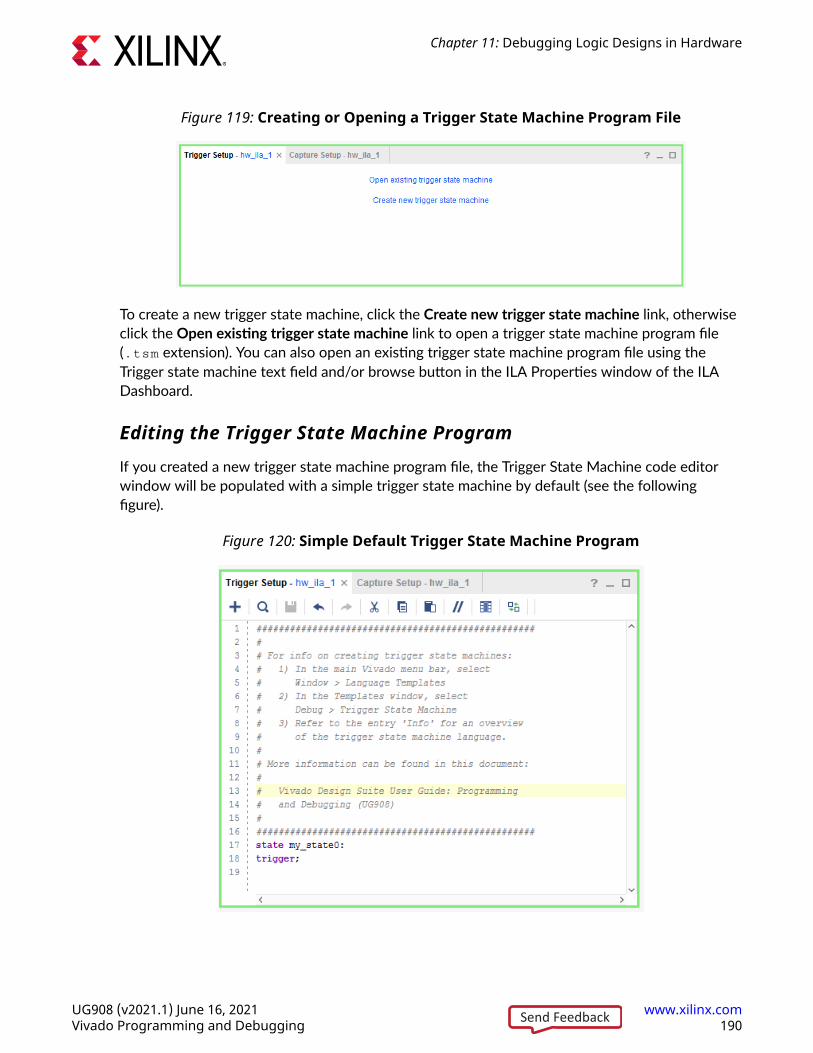
Figure 119: Creating or Opening a Trigger State Machine Program File
To create a new trigger state machine, click the Create new trigger state machine link, otherwiseclick the Open existing trigger state machine link to open a trigger state machine program file(.tsm extension). You can also open an existing trigger state machine program file using theTrigger state machine text field and/or browse button in the ILA Properties window of the ILADashboard.
Editing the Trigger State Machine Program
If you created a new trigger state machine program file, the Trigger State Machine code editorwindow will be populated with a simple trigger state machine by default (see the followingfigure).
Figure 120: Simple Default Trigger State Machine Program
Chapter 11: Debugging Logic Designs in Hardware
UG908 (v2021.1) June 16, 2021 www.xilinx.comVivado Programming and Debugging 190Send Feedback
The simple default trigger state machine program is designed to be valid for any ILA coreconfiguration regardless of debug probe or trigger settings. This means that you can click the RunTrigger for the ILA core without modifying the trigger state machine program.
However, it is likely that you will want to modify the trigger state machine program to implementsome advanced trigger condition. The comment block at the top of the simple state machineshown in the previous figure gives some instructions on how to use the built-in languagetemplates in the Vivado IDE to construct a trigger state machine program (see the followingfigure). A full description of the ILA trigger state machine language, including examples, is foundin Trigger State Machine Language Description.
Figure 121: Trigger State Machine Language Templates
Related Information
Trigger State Machine Language Description
Compiling the Trigger State Machine
The trigger state machine is compiled every time you run the ILA trigger. If you would like tocompile the trigger state machine without running or arming the ILA trigger, click the Compiletrigger state machine button in the ILA Dashboard (see the following figure).
Chapter 11: Debugging Logic Designs in Hardware
UG908 (v2021.1) June 16, 2021 www.xilinx.comVivado Programming and Debugging 191Send Feedback
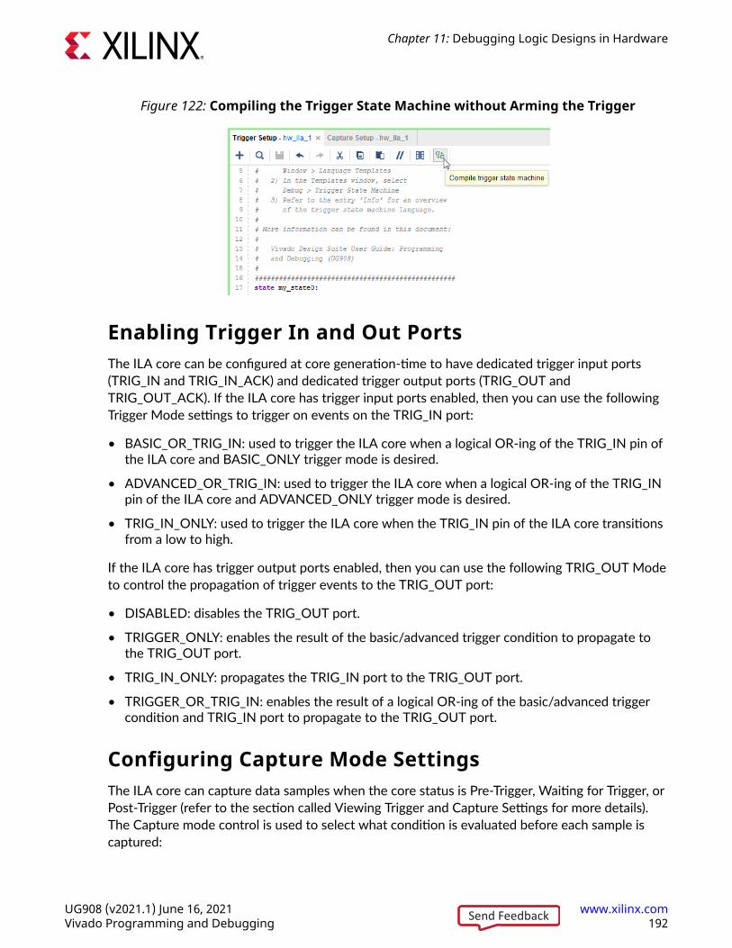
Figure 122: Compiling the Trigger State Machine without Arming the Trigger
Enabling Trigger In and Out PortsThe ILA core can be configured at core generation-time to have dedicated trigger input ports(TRIG_IN and TRIG_IN_ACK) and dedicated trigger output ports (TRIG_OUT andTRIG_OUT_ACK). If the ILA core has trigger input ports enabled, then you can use the followingTrigger Mode settings to trigger on events on the TRIG_IN port:
• BASIC_OR_TRIG_IN: used to trigger the ILA core when a logical OR-ing of the TRIG_IN pin ofthe ILA core and BASIC_ONLY trigger mode is desired.
• ADVANCED_OR_TRIG_IN: used to trigger the ILA core when a logical OR-ing of the TRIG_INpin of the ILA core and ADVANCED_ONLY trigger mode is desired.
• TRIG_IN_ONLY: used to trigger the ILA core when the TRIG_IN pin of the ILA core transitionsfrom a low to high.
If the ILA core has trigger output ports enabled, then you can use the following TRIG_OUT Modeto control the propagation of trigger events to the TRIG_OUT port:
• DISABLED: disables the TRIG_OUT port.
• TRIGGER_ONLY: enables the result of the basic/advanced trigger condition to propagate tothe TRIG_OUT port.
• TRIG_IN_ONLY: propagates the TRIG_IN port to the TRIG_OUT port.
• TRIGGER_OR_TRIG_IN: enables the result of a logical OR-ing of the basic/advanced triggercondition and TRIG_IN port to propagate to the TRIG_OUT port.
Configuring Capture Mode SettingsThe ILA core can capture data samples when the core status is Pre-Trigger, Waiting for Trigger, orPost-Trigger (refer to the section called Viewing Trigger and Capture Settings for more details).The Capture mode control is used to select what condition is evaluated before each sample iscaptured:
Chapter 11: Debugging Logic Designs in Hardware
UG908 (v2021.1) June 16, 2021 www.xilinx.comVivado Programming and Debugging 192Send Feedback
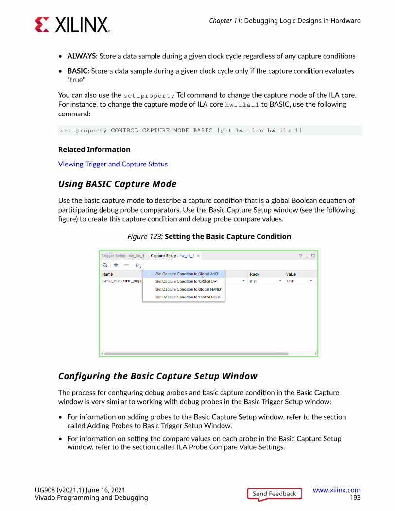
• ALWAYS: Store a data sample during a given clock cycle regardless of any capture conditions
• BASIC: Store a data sample during a given clock cycle only if the capture condition evaluates"true"
You can also use the set_property Tcl command to change the capture mode of the ILA core.For instance, to change the capture mode of ILA core hw_ila_1 to BASIC, use the followingcommand:
set_property CONTROL.CAPTURE_MODE BASIC [get_hw_ilas hw_ila_1]
Related Information
Viewing Trigger and Capture Status
Using BASIC Capture Mode
Use the basic capture mode to describe a capture condition that is a global Boolean equation ofparticipating debug probe comparators. Use the Basic Capture Setup window (see the followingfigure) to create this capture condition and debug probe compare values.
Figure 123: Setting the Basic Capture Condition
Configuring the Basic Capture Setup Window
The process for configuring debug probes and basic capture condition in the Basic Capturewindow is very similar to working with debug probes in the Basic Trigger Setup window:
• For information on adding probes to the Basic Capture Setup window, refer to the sectioncalled Adding Probes to Basic Trigger Setup Window.
• For information on setting the compare values on each probe in the Basic Capture Setupwindow, refer to the section called ILA Probe Compare Value Settings.
Chapter 11: Debugging Logic Designs in Hardware
UG908 (v2021.1) June 16, 2021 www.xilinx.comVivado Programming and Debugging 193Send Feedback
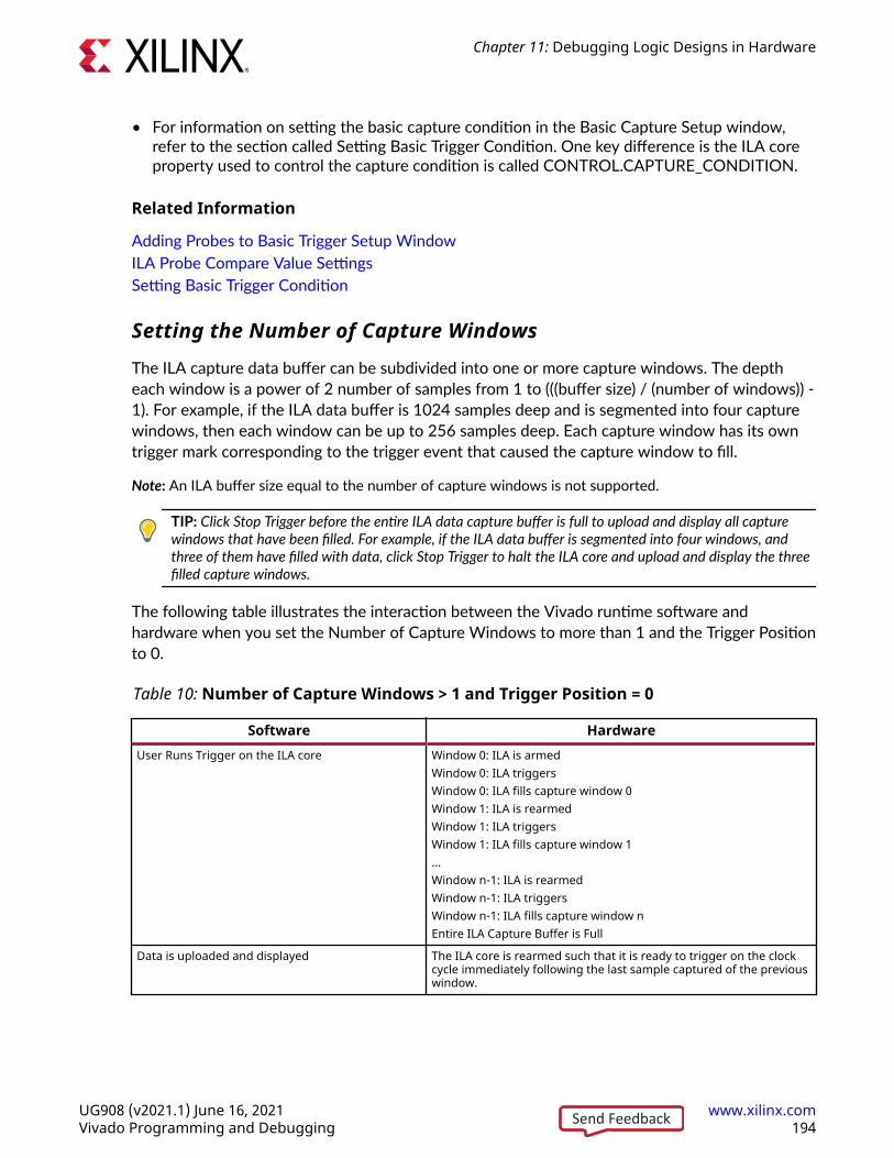
• For information on setting the basic capture condition in the Basic Capture Setup window,refer to the section called Setting Basic Trigger Condition. One key difference is the ILA coreproperty used to control the capture condition is called CONTROL.CAPTURE_CONDITION.
Related Information
Adding Probes to Basic Trigger Setup WindowILA Probe Compare Value SettingsSetting Basic Trigger Condition
Setting the Number of Capture Windows
The ILA capture data buffer can be subdivided into one or more capture windows. The deptheach window is a power of 2 number of samples from 1 to (((buffer size) / (number of windows)) -1). For example, if the ILA data buffer is 1024 samples deep and is segmented into four capturewindows, then each window can be up to 256 samples deep. Each capture window has its owntrigger mark corresponding to the trigger event that caused the capture window to fill.
Note: An ILA buffer size equal to the number of capture windows is not supported.
TIP: Click Stop Trigger before the entire ILA data capture buffer is full to upload and display all capturewindows that have been filled. For example, if the ILA data buffer is segmented into four windows, andthree of them have filled with data, click Stop Trigger to halt the ILA core and upload and display the threefilled capture windows.
The following table illustrates the interaction between the Vivado runtime software andhardware when you set the Number of Capture Windows to more than 1 and the Trigger Positionto 0.
Table 10: Number of Capture Windows > 1 and Trigger Position = 0
Software HardwareUser Runs Trigger on the ILA core Window 0: ILA is armed
Window 0: ILA triggersWindow 0: ILA fills capture window 0Window 1: ILA is rearmedWindow 1: ILA triggersWindow 1: ILA fills capture window 1...Window n-1: ILA is rearmedWindow n-1: ILA triggersWindow n-1: ILA fills capture window nEntire ILA Capture Buffer is Full
Data is uploaded and displayed The ILA core is rearmed such that it is ready to trigger on the clockcycle immediately following the last sample captured of the previouswindow.
Chapter 11: Debugging Logic Designs in Hardware
UG908 (v2021.1) June 16, 2021 www.xilinx.comVivado Programming and Debugging 194Send Feedback

The following table illustrates the interaction between the Vivado runtime software andhardware when you set the Number of Capture Windows to more than 1 and the TriggerPosition to greater than 0.
Table 11: Number of Capture Windows > 1 and Trigger Position > 0
Software HardwareUser Runs Trigger on the ILA core Window 0: ILA is armed
Window 0: ILA fills capture buffer up to trigger positionWindow 0: ILA triggersWindow 0: ILA fills the rest of capture window 0Window 1: ILA is rearmedWindow 1: ILA fills capture buffer up to trigger positionWindow 1: ILA triggersWindow 1: ILA fills capture bufferWindow 1: ILA fills window 1...Window n-1: ILA is rearmedWindow n-1: ILA fills capture buffer up to trigger positionWindow n-1: ILA triggersWindow n-1: ILA fills capture bufferWindow n-1: ILA fills window nEntire ILA Capture Buffer is Full
Data is uploaded and displayed Triggers could be missed between two windows since the ILA nowhas to fill the capture data up to the trigger position.
Setting the Trigger Position in the Capture Window
Use the Trigger position control in the Capture Mode Settings window (or the Trigger Positionproperty in the ILA Core Properties window) to set the position of the trigger marker in thecaptured data window. You can set the trigger position to any sample number in the captureddata window. For instance, in the case of a captured data window that is 1024 samples deep:
• Sample number 0 corresponds to the first (left-most) sample in the captured data window.
• Sample number 1023 corresponds to the last (right-most) sample in the captured datawindow.
• Samples numbers 511 and 512 correspond to the two "center" samples in the captured datawindow.
You can also use the set_property Tcl command to change the ILA core trigger position:
set_property CONTROL.TRIGGER_POSITION 512 [get_hw_ilas hw_ila_1]
Chapter 11: Debugging Logic Designs in Hardware
UG908 (v2021.1) June 16, 2021 www.xilinx.comVivado Programming and Debugging 195Send Feedback

Setting the Data Depth of the Capture Window
Use the Data Depth control in the Capture Mode Settings window (or the Capture data depthproperty in the ILA Core Properties window) to set the data depth of the ILA core's captured datawindow. You can set the data depth to any power of two from 1 to the maximum data depth ofthe ILA core (set during core generation or insertion time).
Note: Refer to the section called Modifying Properties on the Debug Cores for more details on how to setthe maximum capture buffer data depth on ILA cores that are added to the design using the NetlistInsertion probing flow.
You can also use the set_property Tcl command to change the ILA core data depth:
set_property CONTROL.DATA_DEPTH 512 [get_hw_ilas hw_ila_1]
Related Information
Modifying Properties on the Debug Cores
Running the TriggerYou can run or arm the ILA core trigger in two different modes:
• Run Trigger: Selecting the ILA core(s) to be armed followed by clicking the Run Trigger buttonon the ILA Dashboard or Hardware window toolbar arms the ILA core to detect the triggerevent that is defined by the ILA core basic or advanced trigger settings.
• Run Trigger Immediate: Selecting the ILA core(s) to be armed followed by clicking the RunTrigger Immediate button on the ILA Dashboard or Hardware window toolbar arms the ILAcore to trigger immediately regardless of the ILA core trigger settings. This command is usefulfor detecting the "aliveness" of the design by capturing any activity at the probe inputs of theILA core.
You can also arm the trigger by selecting and right-clicking on the ILA core and selecting RunTrigger or Run Trigger Immediate from the popup menu (see the following figure).
Chapter 11: Debugging Logic Designs in Hardware
UG908 (v2021.1) June 16, 2021 www.xilinx.comVivado Programming and Debugging 196Send Feedback
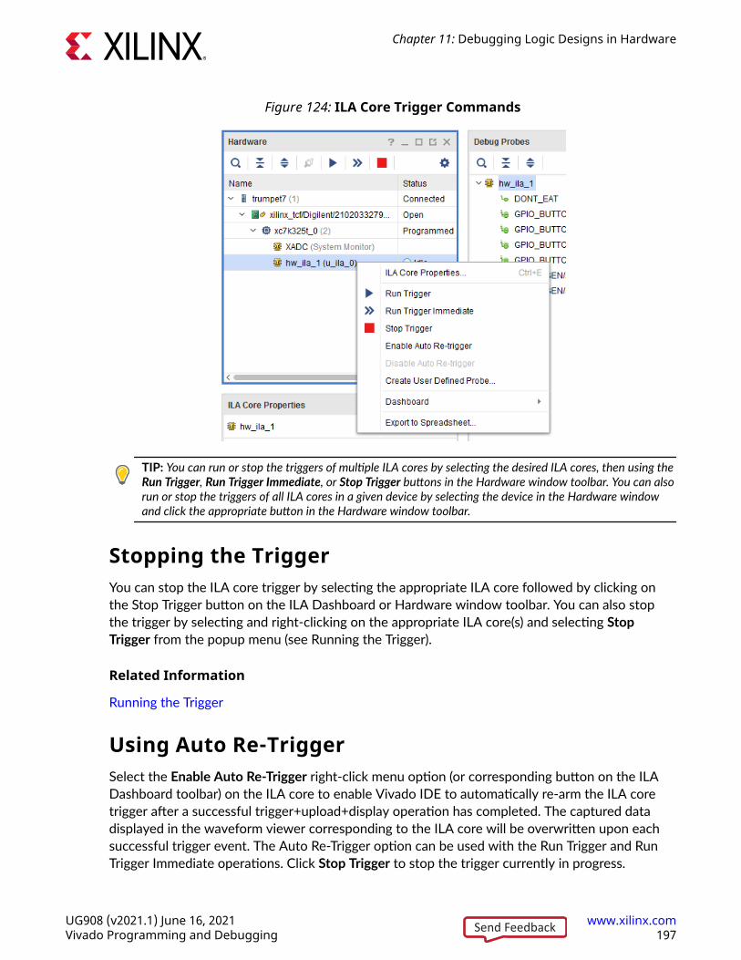
Figure 124: ILA Core Trigger Commands
TIP: You can run or stop the triggers of multiple ILA cores by selecting the desired ILA cores, then using theRun Trigger, Run Trigger Immediate, or Stop Trigger buttons in the Hardware window toolbar. You can alsorun or stop the triggers of all ILA cores in a given device by selecting the device in the Hardware windowand click the appropriate button in the Hardware window toolbar.
Stopping the TriggerYou can stop the ILA core trigger by selecting the appropriate ILA core followed by clicking onthe Stop Trigger button on the ILA Dashboard or Hardware window toolbar. You can also stopthe trigger by selecting and right-clicking on the appropriate ILA core(s) and selecting StopTrigger from the popup menu (see Running the Trigger).
Related Information
Running the Trigger
Using Auto Re-TriggerSelect the Enable Auto Re-Trigger right-click menu option (or corresponding button on the ILADashboard toolbar) on the ILA core to enable Vivado IDE to automatically re-arm the ILA coretrigger after a successful trigger+upload+display operation has completed. The captured datadisplayed in the waveform viewer corresponding to the ILA core will be overwritten upon eachsuccessful trigger event. The Auto Re-Trigger option can be used with the Run Trigger and RunTrigger Immediate operations. Click Stop Trigger to stop the trigger currently in progress.
Chapter 11: Debugging Logic Designs in Hardware
UG908 (v2021.1) June 16, 2021 www.xilinx.comVivado Programming and Debugging 197Send Feedback
The table below illustrates the interaction between the Vivado IDE runtime software andhardware when you invoke the Auto Re-Trigger option.
Table 12: Auto Re-Trigger
Software HardwareClick the Auto Re-trigger option on the ILA core ILA is armed
ILA triggersILA fills capture bufferILA is full
Data is uploaded and displayed ILA is rearmedILA triggersILA fills capture bufferILA is fullLots of cycles are missed between the ILA "full" event and display ofthe ILA data
IMPORTANT! As there is a delay between the time the ILA data is full and the data is uploaded anddisplayed in the GUI, there is a very high probability of missing cycles between these events where the ILAcould have triggered.
Viewing Trigger and Capture StatusThe ILA debug core trigger and capture status is displayed in two places in Vivado IDE:
• In the Hardware window Status column of the row(s) corresponding to the ILA debug core(s).
• In the Trigger Capture Status window of the ILA Dashboard.
The Status column in the Hardware window indicates the current state or status of each ILA core(see the following table).
Table 13: ILA Core Status Description
ILA CoreStatus Description
Idle The ILA core is idle and waiting for its trigger to be run. If the trigger position is 0, then the ILA core willtransition to the Waiting for Trigger status once the trigger is run, otherwise the ILA core will transitionto the Pre-Trigger status.
Pre-Trigger The ILA core is capturing pre-trigger data into its data capture window. Once the pre-trigger data hasbeen captured, the ILA core will transition to the Waiting for Trigger status.
Waiting forTrigger
The ILA core trigger is armed and is waiting for the trigger event to occur as described by the basic oradvanced trigger settings. Once the trigger occurs, the ILA core will transition to the Full status if thetrigger position is set to the last data sample in the capture window, otherwise it will transition to thePost-Trigger status.
Post-Trigger The ILA core is capturing post-trigger data into its data capture window. Once the post-trigger data hasbeen captured, the ILA core will transition to the Full status.
Full The ILA core capture buffer is full and is being uploaded to the host for display. The ILA core willtransition to the Idle status once the data has been uploaded and displayed.
Chapter 11: Debugging Logic Designs in Hardware
UG908 (v2021.1) June 16, 2021 www.xilinx.comVivado Programming and Debugging 198Send Feedback
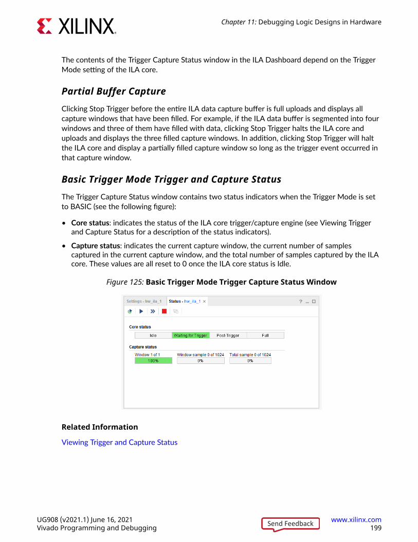
The contents of the Trigger Capture Status window in the ILA Dashboard depend on the TriggerMode setting of the ILA core.
Partial Buffer Capture
Clicking Stop Trigger before the entire ILA data capture buffer is full uploads and displays allcapture windows that have been filled. For example, if the ILA data buffer is segmented into fourwindows and three of them have filled with data, clicking Stop Trigger halts the ILA core anduploads and displays the three filled capture windows. In addition, clicking Stop Trigger will haltthe ILA core and display a partially filled capture window so long as the trigger event occurred inthat capture window.
Basic Trigger Mode Trigger and Capture Status
The Trigger Capture Status window contains two status indicators when the Trigger Mode is setto BASIC (see the following figure):
• Core status: indicates the status of the ILA core trigger/capture engine (see Viewing Triggerand Capture Status for a description of the status indicators).
• Capture status: indicates the current capture window, the current number of samplescaptured in the current capture window, and the total number of samples captured by the ILAcore. These values are all reset to 0 once the ILA core status is Idle.
Figure 125: Basic Trigger Mode Trigger Capture Status Window
Related Information
Viewing Trigger and Capture Status
Chapter 11: Debugging Logic Designs in Hardware
UG908 (v2021.1) June 16, 2021 www.xilinx.comVivado Programming and Debugging 199Send Feedback
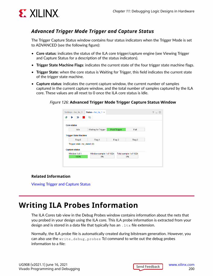
Advanced Trigger Mode Trigger and Capture Status
The Trigger Capture Status window contains four status indicators when the Trigger Mode is setto ADVANCED (see the following figure):
• Core status: indicates the status of the ILA core trigger/capture engine (see Viewing Triggerand Capture Status for a description of the status indicators).
• Trigger State Machine Flags: indicates the current state of the four trigger state machine flags.
• Trigger State: when the core status is Waiting for Trigger, this field indicates the current stateof the trigger state machine.
• Capture status: indicates the current capture window, the current number of samplescaptured in the current capture window, and the total number of samples captured by the ILAcore. These values are all reset to 0 once the ILA core status is Idle.
Figure 126: Advanced Trigger Mode Trigger Capture Status Window
Related Information
Viewing Trigger and Capture Status
Writing ILA Probes InformationThe ILA Cores tab view in the Debug Probes window contains information about the nets thatyou probed in your design using the ILA core. This ILA probe information is extracted from yourdesign and is stored in a data file that typically has an .ltx file extension.
Normally, the ILA probe file is automatically created during bitstream generation. However, youcan also use the write_debug_probes Tcl command to write out the debug probesinformation to a file:
Chapter 11: Debugging Logic Designs in Hardware
UG908 (v2021.1) June 16, 2021 www.xilinx.comVivado Programming and Debugging 200Send Feedback
1. If you are in project mode, open the Implemented Design. If you are in non-project mode,open the implemented design checklist.
2. Run the write_debug_probes filename.ltx Tcl command.
Reading ILA Probes InformationThe ILA probe file is automatically associated with the FPGA or ACAP hardware device if theprobes file is called debug_nets.ltx and is found in the same directory as the bitstreamprogramming (.bit) file that is associated with the device.
You can also specify the location of the probes file:
1. Select the FPGA or ACAP in the Hardware window.
2. Set the Probes file location in the Hardware Device Properties window.
3. Click Apply to apply the change.
You can also set the location using the set_property Tcl command:
set_property PROBES.FILE {C:/myprobes.ltx} [lindex [get_hw_devices] 0]
Viewing Captured Data from the ILA Core inthe Waveform Viewer
Once the ILA core captured data has been uploaded to the Vivado IDE, it is displayed in theWaveform Viewer. See Viewing ILA Probe Data for details on using the Waveform Viewer toview captured data from the ILA core.
Related Information
Viewing ILA Probe Data in the Waveform Viewer
Using Waveform ILA Trigger and ExportFeatures
You can use the icons in the waveform window to arm ILAs and run trigger, stop the trigger, andexport ILA data as shown below.
Chapter 11: Debugging Logic Designs in Hardware
UG908 (v2021.1) June 16, 2021 www.xilinx.comVivado Programming and Debugging 201Send Feedback
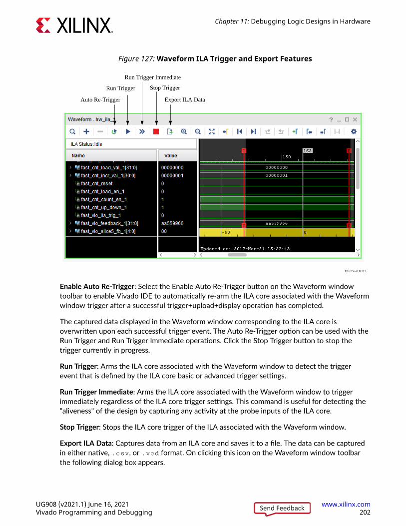
Figure 127: Waveform ILA Trigger and Export Features
Auto Re-Trigger
Run Trigger
Run Trigger Immediate
Stop Trigger
Export ILA Data
X16755-032717
Enable Auto Re-Trigger: Select the Enable Auto Re-Trigger button on the Waveform windowtoolbar to enable Vivado IDE to automatically re-arm the ILA core associated with the Waveformwindow trigger after a successful trigger+upload+display operation has completed.
The captured data displayed in the Waveform window corresponding to the ILA core isoverwritten upon each successful trigger event. The Auto Re-Trigger option can be used with theRun Trigger and Run Trigger Immediate operations. Click the Stop Trigger button to stop thetrigger currently in progress.
Run Trigger: Arms the ILA core associated with the Waveform window to detect the triggerevent that is defined by the ILA core basic or advanced trigger settings.
Run Trigger Immediate: Arms the ILA core associated with the Waveform window to triggerimmediately regardless of the ILA core trigger settings. This command is useful for detecting the"aliveness" of the design by capturing any activity at the probe inputs of the ILA core.
Stop Trigger: Stops the ILA core trigger of the ILA associated with the Waveform window.
Export ILA Data: Captures data from an ILA core and saves it to a file. The data can be capturedin either native, .csv, or .vcd format. On clicking this icon on the Waveform window toolbarthe following dialog box appears.
Chapter 11: Debugging Logic Designs in Hardware
UG908 (v2021.1) June 16, 2021 www.xilinx.comVivado Programming and Debugging 202Send Feedback
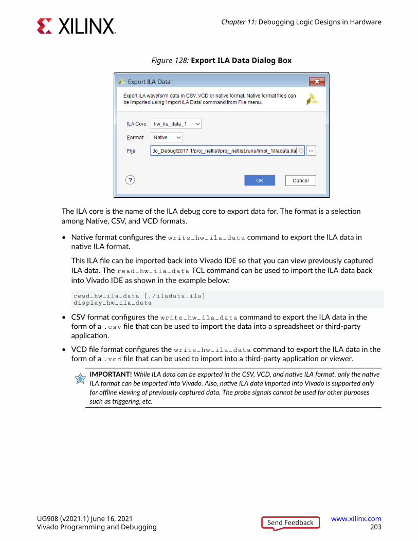
Figure 128: Export ILA Data Dialog Box
The ILA core is the name of the ILA debug core to export data for. The format is a selectionamong Native, CSV, and VCD formats.
• Native format configures the write_hw_ila_data command to export the ILA data innative ILA format.
This ILA file can be imported back into Vivado IDE so that you can view previously capturedILA data. The read_hw_ila_data TCL command can be used to import the ILA data backinto Vivado IDE as shown in the example below:
read_hw_ila_data {./iladata.ila}display_hw_ila_data
• CSV format configures the write_hw_ila_data command to export the ILA data in theform of a .csv file that can be used to import the data into a spreadsheet or third-partyapplication.
• VCD file format configures the write_hw_ila_data command to export the ILA data in theform of a .vcd file that can be used to import into a third-party application or viewer.
IMPORTANT! While ILA data can be exported in the CSV, VCD, and native ILA format, only the nativeILA format can be imported into Vivado. Also, native ILA data imported into Vivado is supported onlyfor offline viewing of previously captured data. The probe signals cannot be used for other purposessuch as triggering, etc.
Chapter 11: Debugging Logic Designs in Hardware
UG908 (v2021.1) June 16, 2021 www.xilinx.comVivado Programming and Debugging 203Send Feedback
Saving and Restoring Captured Data from theILA Core
In addition to displaying the captured data that is directly uploaded from the ILA core, you canalso write the captured data to a file then read the data from a file and display it in the waveformviewer.
Saving Captured ILA Data to a FileCurrently, the only way to upload captured data from an ILA core and save it to a file is to use thefollowing Tcl command:
write_hw_ila_data my_hw_ila_data_file.ila [upload_hw_ila_data hw_ila_1]
This Tcl command sequence uploads the captured data from the ILA core and writes it to anarchive file called my_hw_ila_data_file.ila. The archive file contains the waveformdatabase file, the waveform configuration file, a waveform comma separated value file, and adebug probes file.
TIP: Use the -csv_file option to generate a comma-separated values (CSV) file. This configures thewrite_hw_ila_data command to export the ILA data in the form of a CSV file that can be used toimport into a spreadsheet or third-party application, rather than the default binary ILA file format.
TIP: Use the -vcd_file option to generate a value change dump (VCD) file. This configures thewrite_hw_ila_data command to export the ILA data in the form of a VCD file that can be used toimport into a third-party application or viewer, rather than the default binary ILA file format.
Probe Data Radix
Every probe has a DISPLAY_RADIX property associated with it. This property is set to HEX for amulti-bit probe and BINARY for a one-bit probe by default. The exported probe data in the .csvfiles use probe radix.
You can change the DISPLAY_RADIX property of all the probes of all ILAs in the design asfollows in the Vivado Hardware Manager Tcl Console:
foreach probe [get_hw_probes -of [get_hw_ilas]] { set_property DISPLAY_RADIX binary $probe set_property DISPLAY_AS_ENUM false $probe }
Chapter 11: Debugging Logic Designs in Hardware
UG908 (v2021.1) June 16, 2021 www.xilinx.comVivado Programming and Debugging 204Send Feedback
Note: Here we are changing the radix of all the probes in all the ILAs to BINARY. To change the radix toHEX, use the script below.
foreach probe [get_hw_probes -of [get_hw_ilas]] { set_property DISPLAY_RADIX hex $probe set_property DISPLAY_AS_ENUM false $probe }
Listing data samples associated with a single probe
You can also list data samples associated with individual probes using the list_hw_samplesTcl command.
An example of listing the samples associated with probe fast_cnt_incr_val_1 on ILAnamed i_fast_ila is shown below:
list_hw_samples [get_hw_probes fast_cnt_incr_val_1 -of_objects [get_hw_ilas -of_objects [get_hw_devices xc7k325t_0] -filter {CELL_NAME=~"i_fast_ila"}]]00000001 00000001 00000001 00000001 00000001 00000001 00000001 00000001 00000001 00000001 00000001 00000001 00000001 00000001 00000001 00000001 00000001 00000001 00000001 00000001 00000001 00000001 00000001 00000001 00000001 00000001 00000001 00000001 00000001 00000001 00000001 00000001 00000001 00000001 00000001 00000001...
Restoring Captured ILA Data from a FileCurrently, the only way to restore captured data from a file and display it in the waveform vieweris to use the following Tcl command:
display_hw_ila_data [read_hw_ila_data my_hw_ila_data_file.ila]
This Tcl command sequence reads the previously saved captured data from the ILA core anddisplays it in the Waveform window.
Note: The waveform configuration settings (dividers, markers, colors, probe radices, etc.) for the ILA DataWaveform window is also saved in the ILA captured data archive file. Restoring and displaying anypreviously saved ILA data uses these stored waveform configuration settings.
IMPORTANT! Do NOT use the open_wave_config command to open a waveform created from ILAcaptured data. This is a simulator-only command and will not function correctly with ILA captured datawaveforms.
Chapter 11: Debugging Logic Designs in Hardware
UG908 (v2021.1) June 16, 2021 www.xilinx.comVivado Programming and Debugging 205Send Feedback
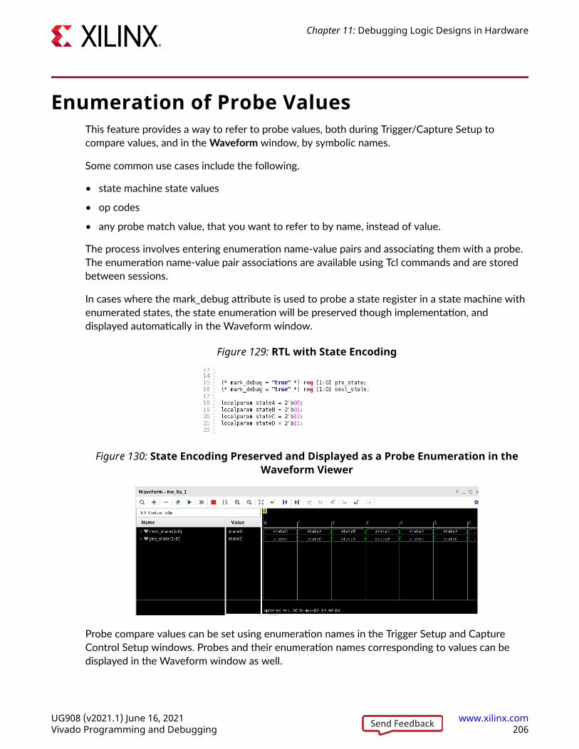
Enumeration of Probe ValuesThis feature provides a way to refer to probe values, both during Trigger/Capture Setup tocompare values, and in the Waveform window, by symbolic names.
Some common use cases include the following.
• state machine state values
• op codes
• any probe match value, that you want to refer to by name, instead of value.
The process involves entering enumeration name-value pairs and associating them with a probe.The enumeration name-value pair associations are available using Tcl commands and are storedbetween sessions.
In cases where the mark_debug attribute is used to probe a state register in a state machine withenumerated states, the state enumeration will be preserved though implementation, anddisplayed automatically in the Waveform window.
Figure 129: RTL with State Encoding
Figure 130: State Encoding Preserved and Displayed as a Probe Enumeration in theWaveform Viewer
Probe compare values can be set using enumeration names in the Trigger Setup and CaptureControl Setup windows. Probes and their enumeration names corresponding to values can bedisplayed in the Waveform window as well.
Chapter 11: Debugging Logic Designs in Hardware
UG908 (v2021.1) June 16, 2021 www.xilinx.comVivado Programming and Debugging 206Send Feedback
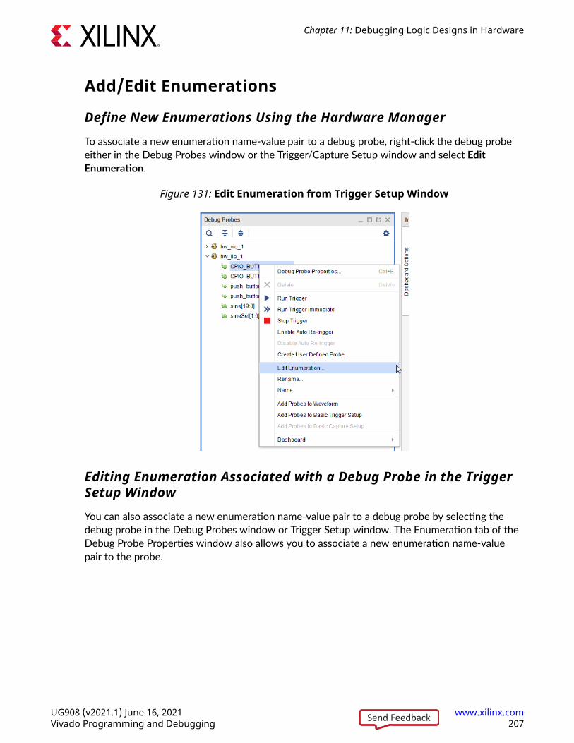
Add/Edit Enumerations
Define New Enumerations Using the Hardware Manager
To associate a new enumeration name-value pair to a debug probe, right-click the debug probeeither in the Debug Probes window or the Trigger/Capture Setup window and select EditEnumeration.
Figure 131: Edit Enumeration from Trigger Setup Window
Editing Enumeration Associated with a Debug Probe in the TriggerSetup Window
You can also associate a new enumeration name-value pair to a debug probe by selecting thedebug probe in the Debug Probes window or Trigger Setup window. The Enumeration tab of theDebug Probe Properties window also allows you to associate a new enumeration name-valuepair to the probe.
Chapter 11: Debugging Logic Designs in Hardware
UG908 (v2021.1) June 16, 2021 www.xilinx.comVivado Programming and Debugging 207Send Feedback
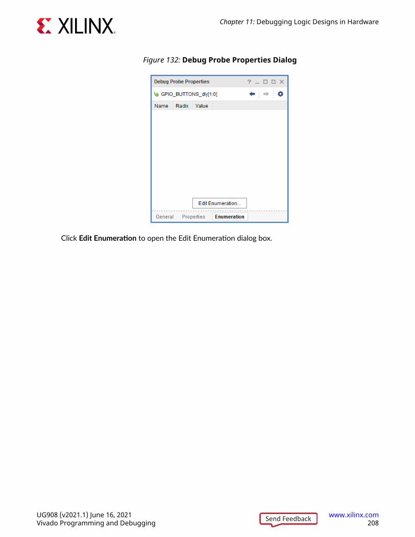
Figure 132: Debug Probe Properties Dialog
Click Edit Enumeration to open the Edit Enumeration dialog box.
Chapter 11: Debugging Logic Designs in Hardware
UG908 (v2021.1) June 16, 2021 www.xilinx.comVivado Programming and Debugging 208Send Feedback
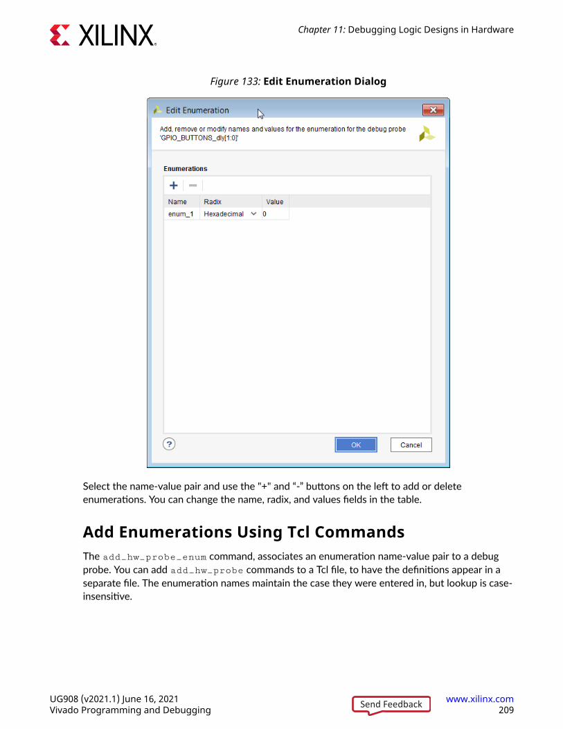
Figure 133: Edit Enumeration Dialog
Select the name-value pair and use the "+" and “-” buttons on the left to add or deleteenumerations. You can change the name, radix, and values fields in the table.
Add Enumerations Using Tcl CommandsThe add_hw_probe_enum command, associates an enumeration name-value pair to a debugprobe. You can add add_hw_probe commands to a Tcl file, to have the definitions appear in aseparate file. The enumeration names maintain the case they were entered in, but lookup is case-insensitive.
Chapter 11: Debugging Logic Designs in Hardware
UG908 (v2021.1) June 16, 2021 www.xilinx.comVivado Programming and Debugging 209Send Feedback
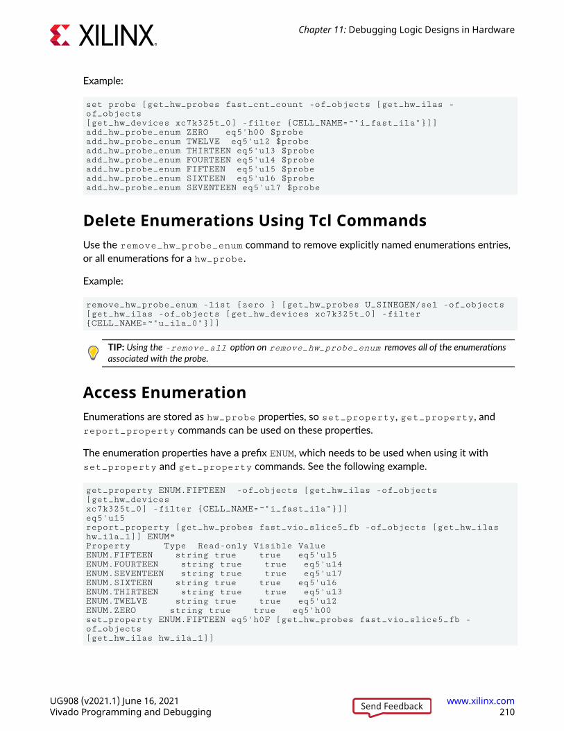
Example:
set probe [get_hw_probes fast_cnt_count -of_objects [get_hw_ilas -of_objects [get_hw_devices xc7k325t_0] -filter {CELL_NAME=~"i_fast_ila"}]]add_hw_probe_enum ZERO eq5'h00 $probeadd_hw_probe_enum TWELVE eq5'u12 $probeadd_hw_probe_enum THIRTEEN eq5'u13 $probeadd_hw_probe_enum FOURTEEN eq5'u14 $probeadd_hw_probe_enum FIFTEEN eq5'u15 $probeadd_hw_probe_enum SIXTEEN eq5'u16 $probeadd_hw_probe_enum SEVENTEEN eq5'u17 $probe
Delete Enumerations Using Tcl CommandsUse the remove_hw_probe_enum command to remove explicitly named enumerations entries,or all enumerations for a hw_probe.
Example:
remove_hw_probe_enum -list {zero } [get_hw_probes U_SINEGEN/sel -of_objects [get_hw_ilas -of_objects [get_hw_devices xc7k325t_0] -filter {CELL_NAME=~"u_ila_0"}]]
TIP: Using the -remove_all option on remove_hw_probe_enum removes all of the enumerationsassociated with the probe.
Access EnumerationEnumerations are stored as hw_probe properties, so set_property, get_property, andreport_property commands can be used on these properties.
The enumeration properties have a prefix ENUM, which needs to be used when using it withset_property and get_property commands. See the following example.
get_property ENUM.FIFTEEN -of_objects [get_hw_ilas -of_objects [get_hw_devices xc7k325t_0] -filter {CELL_NAME=~"i_fast_ila"}]]eq5'u15report_property [get_hw_probes fast_vio_slice5_fb -of_objects [get_hw_ilas hw_ila_1]] ENUM*Property Type Read-only Visible ValueENUM.FIFTEEN string true true eq5'u15ENUM.FOURTEEN string true true eq5'u14ENUM.SEVENTEEN string true true eq5'u17ENUM.SIXTEEN string true true eq5'u16ENUM.THIRTEEN string true true eq5'u13ENUM.TWELVE string true true eq5'u12ENUM.ZERO string true true eq5'h00set_property ENUM.FIFTEEN eq5'h0F [get_hw_probes fast_vio_slice5_fb -of_objects [get_hw_ilas hw_ila_1]]
Chapter 11: Debugging Logic Designs in Hardware
UG908 (v2021.1) June 16, 2021 www.xilinx.comVivado Programming and Debugging 210Send Feedback
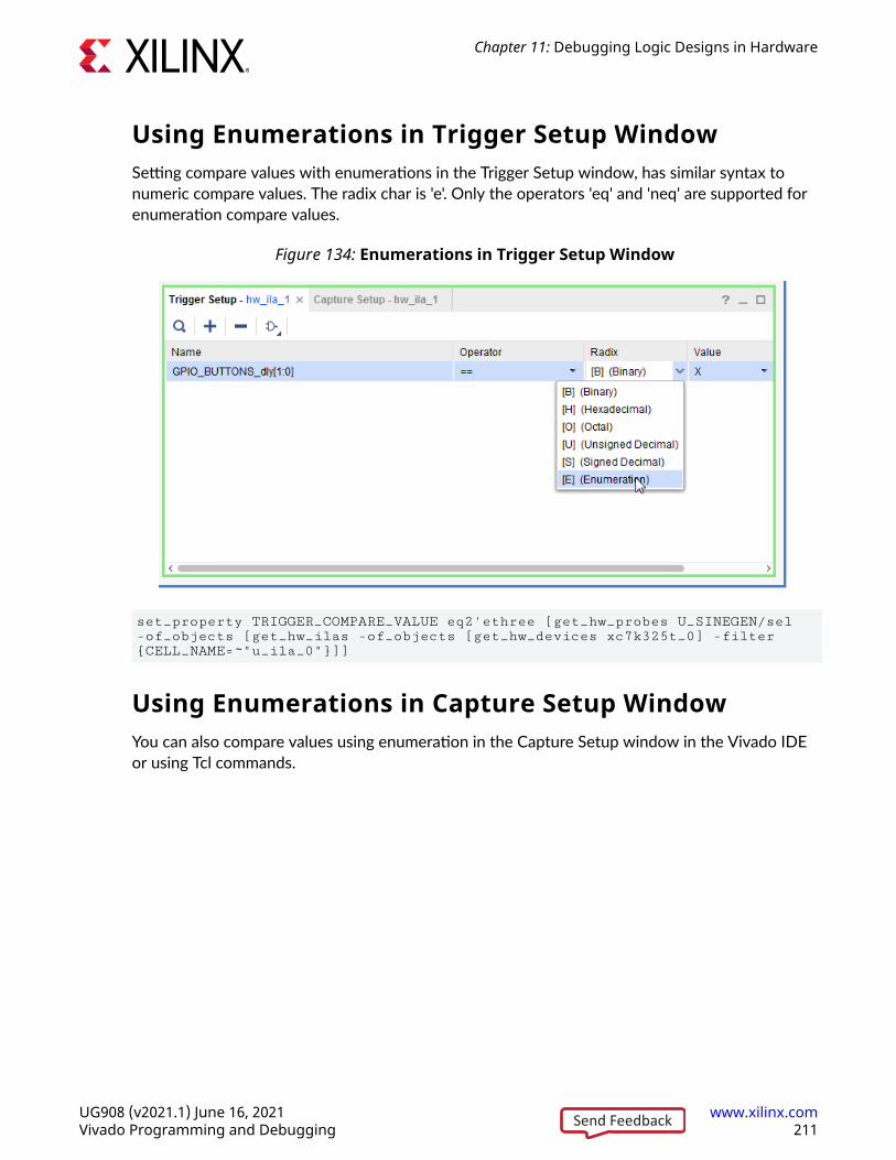
Using Enumerations in Trigger Setup WindowSetting compare values with enumerations in the Trigger Setup window, has similar syntax tonumeric compare values. The radix char is 'e'. Only the operators 'eq' and 'neq' are supported forenumeration compare values.
Figure 134: Enumerations in Trigger Setup Window
set_property TRIGGER_COMPARE_VALUE eq2'ethree [get_hw_probes U_SINEGEN/sel -of_objects [get_hw_ilas -of_objects [get_hw_devices xc7k325t_0] -filter {CELL_NAME=~"u_ila_0"}]]
Using Enumerations in Capture Setup WindowYou can also compare values using enumeration in the Capture Setup window in the Vivado IDEor using Tcl commands.
Chapter 11: Debugging Logic Designs in Hardware
UG908 (v2021.1) June 16, 2021 www.xilinx.comVivado Programming and Debugging 211Send Feedback
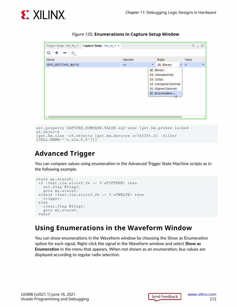
Figure 135: Enumerations in Capture Setup Window
set_property CAPTURE_COMPARE_VALUE eq2'eone [get_hw_probes locked -of_objects [get_hw_ilas -of_objects [get_hw_devices xc7k325t_0] -filter {CELL_NAME=~"u_ila_0_0"}]]
Advanced TriggerYou can compare values using enumeration in the Advanced Trigger State Machine scripts as inthe following example.
state my_state0: if (fast_ila_slice5_fb == 5'eFIFTEEN) then set_flag $flag1; goto my_state0; elseif (fast_ila_slice5_fb == 5'eTWELVE) then trigger; else clear_flag $flag1; goto my_state0; endif
Using Enumerations in the Waveform WindowYou can show enumerations in the Waveform window by choosing the Show as Enumerationoption for each signal. Right-click the signal in the Waveform window and select Show asEnumeration in the menu that appears. When not shown as an enumeration, bus values aredisplayed according to regular radix selection.
Chapter 11: Debugging Logic Designs in Hardware
UG908 (v2021.1) June 16, 2021 www.xilinx.comVivado Programming and Debugging 212Send Feedback
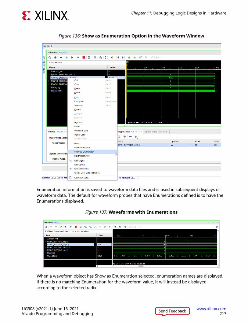
Figure 136: Show as Enumeration Option in the Waveform Window
Enumeration information is saved to waveform data files and is used in subsequent displays ofwaveform data. The default for waveform probes that have Enumerations defined is to have theEnumerations displayed.
Figure 137: Waveforms with Enumerations
When a waveform object has Show as Enumeration selected, enumeration names are displayed.If there is no matching Enumeration for the waveform value, it will instead be displayedaccording to the selected radix.
Chapter 11: Debugging Logic Designs in Hardware
UG908 (v2021.1) June 16, 2021 www.xilinx.comVivado Programming and Debugging 213Send Feedback
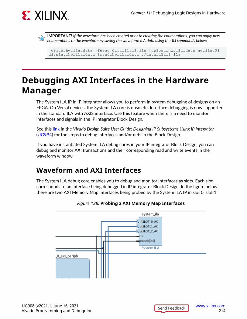
IMPORTANT! If the waveform has been created prior to creating the enumerations, you can apply newenumerations to the waveform by saving the waveform ILA data using the Tcl commands below:
write_hw_ila_data -force data_ila_3.ila [upload_hw_ila_data hw_ila_3]display_hw_ila_data [read_hw_ila_data ./data_ila_3.ila]
Debugging AXI Interfaces in the HardwareManager
The System ILA IP in IP integrator allows you to perform in-system debugging of designs on anFPGA. On Versal devices, the System ILA core is obsolete. Interface debugging is now supportedin the standard ILA with AXIS interface. Use this feature when there is a need to monitorinterfaces and signals in the IP integrator Block Design.
See this link in the Vivado Design Suite User Guide: Designing IP Subsystems Using IP Integrator(UG994) for the steps to debug interfaces and/or nets in the Block Design.
If you have instantiated System ILA debug cores in your IP integrator Block Design, you candebug and monitor AXI transactions and their corresponding read and write events in thewaveform window.
Waveform and AXI InterfacesThe System ILA debug core enables you to debug and monitor interfaces as slots. Each slotcorresponds to an interface being debugged in IP integrator Block Design. In the figure belowthere are two AXI Memory Map interfaces being probed by the System ILA IP in slot 0, slot 1.
Figure 138: Probing 2 AXI Memory Map Interfaces
Chapter 11: Debugging Logic Designs in Hardware
UG908 (v2021.1) June 16, 2021 www.xilinx.comVivado Programming and Debugging 214Send Feedback
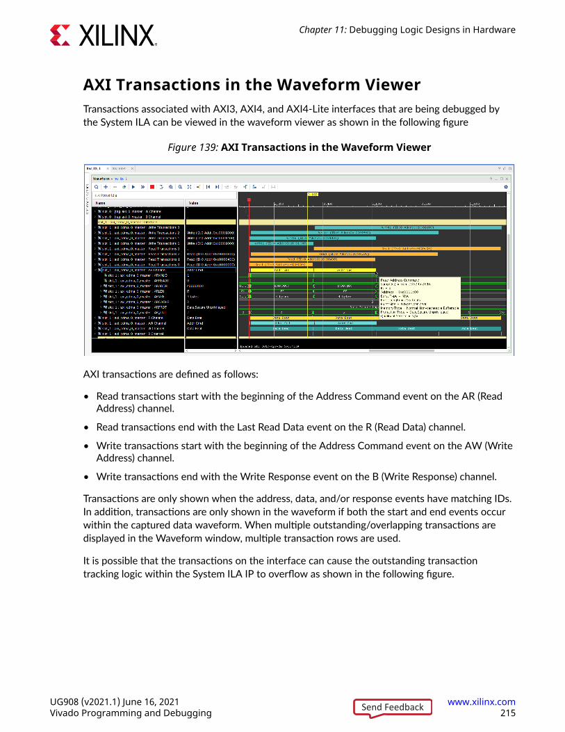
AXI Transactions in the Waveform ViewerTransactions associated with AXI3, AXI4, and AXI4-Lite interfaces that are being debugged bythe System ILA can be viewed in the waveform viewer as shown in the following figure
Figure 139: AXI Transactions in the Waveform Viewer
AXI transactions are defined as follows:
• Read transactions start with the beginning of the Address Command event on the AR (ReadAddress) channel.
• Read transactions end with the Last Read Data event on the R (Read Data) channel.
• Write transactions start with the beginning of the Address Command event on the AW (WriteAddress) channel.
• Write transactions end with the Write Response event on the B (Write Response) channel.
Transactions are only shown when the address, data, and/or response events have matching IDs.In addition, transactions are only shown in the waveform if both the start and end events occurwithin the captured data waveform. When multiple outstanding/overlapping transactions aredisplayed in the Waveform window, multiple transaction rows are used.
It is possible that the transactions on the interface can cause the outstanding transactiontracking logic within the System ILA IP to overflow as shown in the following figure.
Chapter 11: Debugging Logic Designs in Hardware
UG908 (v2021.1) June 16, 2021 www.xilinx.comVivado Programming and Debugging 215Send Feedback
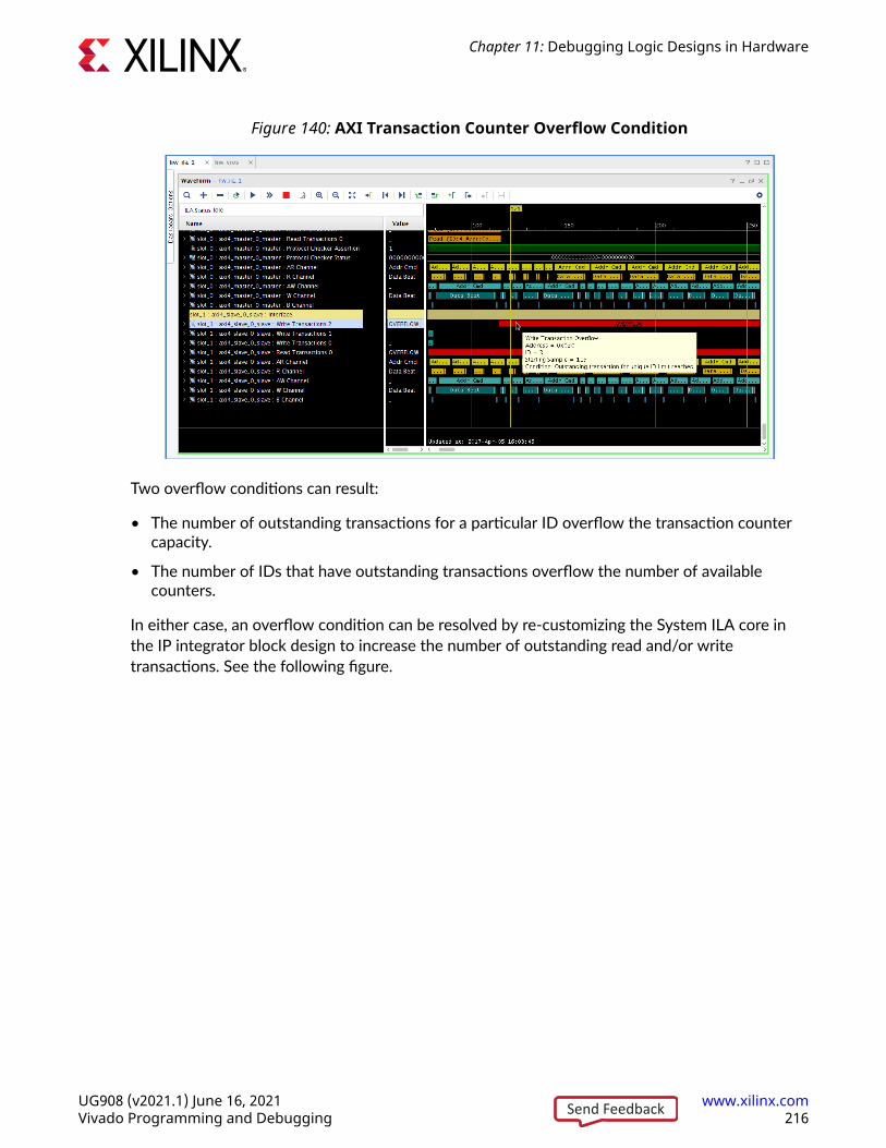
Figure 140: AXI Transaction Counter Overflow Condition
Two overflow conditions can result:
• The number of outstanding transactions for a particular ID overflow the transaction countercapacity.
• The number of IDs that have outstanding transactions overflow the number of availablecounters.
In either case, an overflow condition can be resolved by re-customizing the System ILA core inthe IP integrator block design to increase the number of outstanding read and/or writetransactions. See the following figure.
Chapter 11: Debugging Logic Designs in Hardware
UG908 (v2021.1) June 16, 2021 www.xilinx.comVivado Programming and Debugging 216Send Feedback
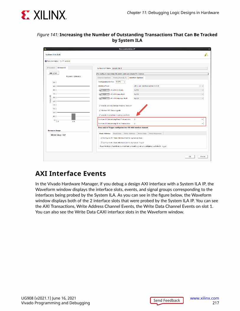
Figure 141: Increasing the Number of Outstanding Transactions That Can Be Trackedby System ILA
AXI Interface EventsIn the Vivado Hardware Manager, if you debug a design AXI interface with a System ILA IP, theWaveform window displays the interface slots, events, and signal groups corresponding to theinterfaces being probed by the System ILA. As you can see in the figure below, the Waveformwindow displays both of the 2 interface slots that were probed by the System ILA IP. You can seethe AXI Transactions, Write Address Channel Events, the Write Data Channel Events on slot 1.You can also see the Write Data CAXI interface slots in the Waveform window.
Chapter 11: Debugging Logic Designs in Hardware
UG908 (v2021.1) June 16, 2021 www.xilinx.comVivado Programming and Debugging 217Send Feedback
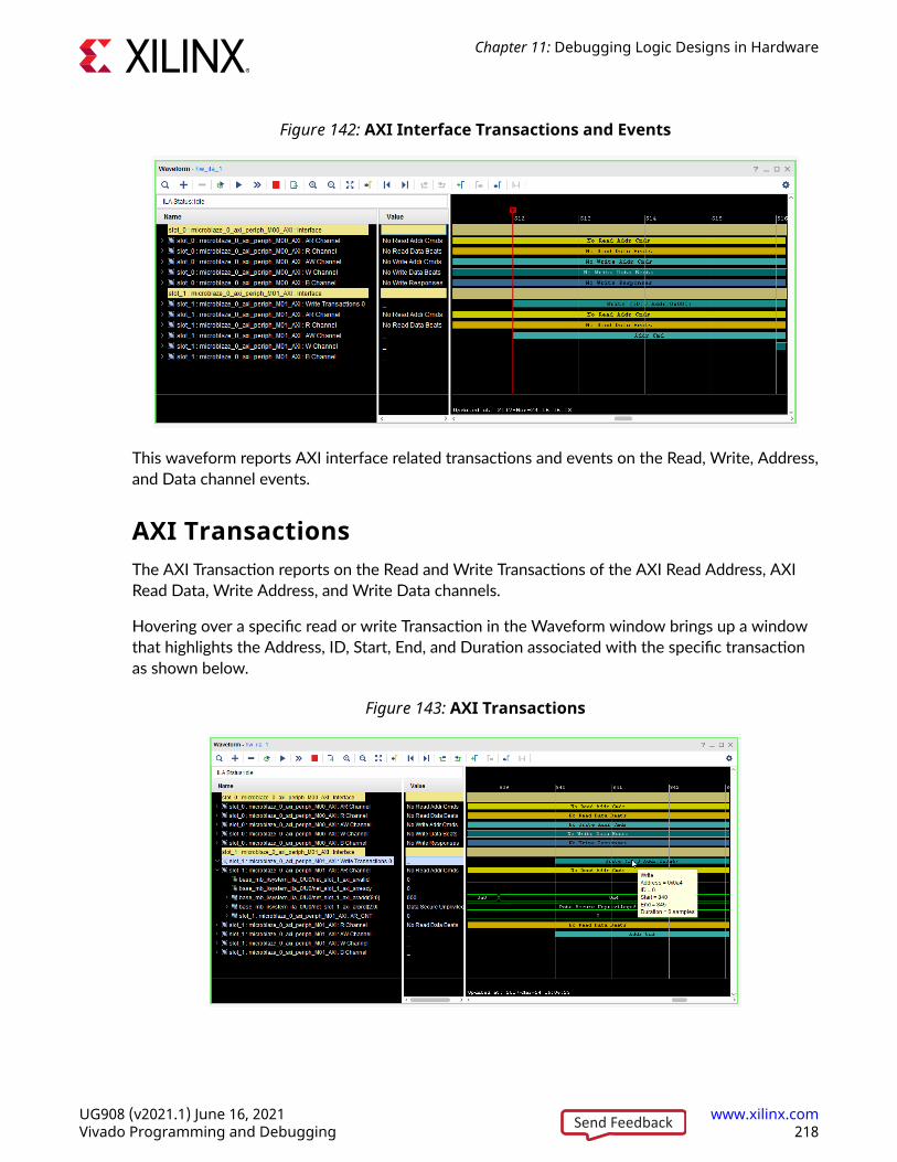
Figure 142: AXI Interface Transactions and Events
This waveform reports AXI interface related transactions and events on the Read, Write, Address,and Data channel events.
AXI TransactionsThe AXI Transaction reports on the Read and Write Transactions of the AXI Read Address, AXIRead Data, Write Address, and Write Data channels.
Hovering over a specific read or write Transaction in the Waveform window brings up a windowthat highlights the Address, ID, Start, End, and Duration associated with the specific transactionas shown below.
Figure 143: AXI Transactions
Chapter 11: Debugging Logic Designs in Hardware
UG908 (v2021.1) June 16, 2021 www.xilinx.comVivado Programming and Debugging 218Send Feedback
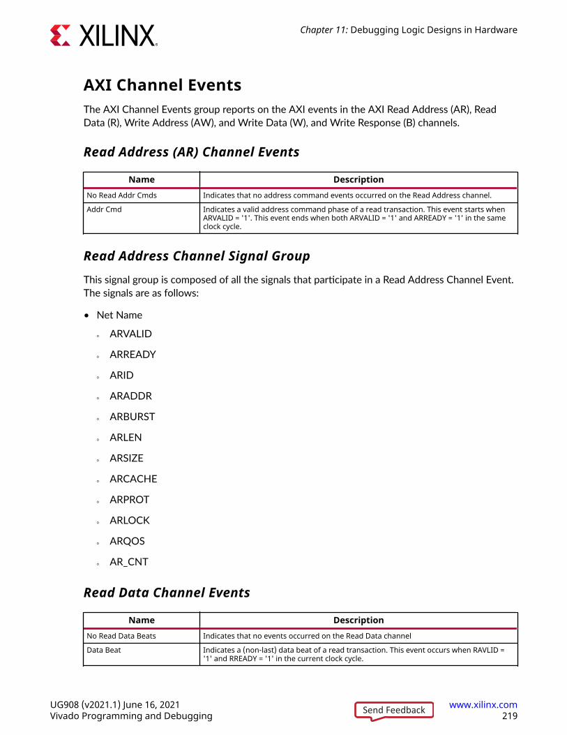
AXI Channel EventsThe AXI Channel Events group reports on the AXI events in the AXI Read Address (AR), ReadData (R), Write Address (AW), and Write Data (W), and Write Response (B) channels.
Read Address (AR) Channel Events
Name DescriptionNo Read Addr Cmds Indicates that no address command events occurred on the Read Address channel.
Addr Cmd Indicates a valid address command phase of a read transaction. This event starts whenARVALID = '1'. This event ends when both ARVALID = '1' and ARREADY = '1' in the sameclock cycle.
Read Address Channel Signal Group
This signal group is composed of all the signals that participate in a Read Address Channel Event.The signals are as follows:
• Net Name
○ ARVALID
○ ARREADY
○ ARID
○ ARADDR
○ ARBURST
○ ARLEN
○ ARSIZE
○ ARCACHE
○ ARPROT
○ ARLOCK
○ ARQOS
○ AR_CNT
Read Data Channel Events
Name DescriptionNo Read Data Beats Indicates that no events occurred on the Read Data channel
Data Beat Indicates a (non-last) data beat of a read transaction. This event occurs when RAVLID ='1' and RREADY = '1' in the current clock cycle.
Chapter 11: Debugging Logic Designs in Hardware
UG908 (v2021.1) June 16, 2021 www.xilinx.comVivado Programming and Debugging 219Send Feedback
Name DescriptionLast Data Indicates the last data beat of a read transaction. This event occurs when RVALID = '1'
and RREADY = '1' and RLAST = '1' in the current clock cycle.
Read Data Channel Signal Group
This signal group is composed of all the signals that participate in a Read Data Channel Event.The signals are as follows:
• Net Name
○ RVALID
○ RREADY
○ RLAST
○ RID
○ RDATA
○ RRESP
○ R_CNT
Write Address Channel Events
Name DescriptionNo Write Addr Cmds Indicates that no address command events occurred on the Write Address channel.
Addr Cmd Indicates a valid address command phase of a write transaction. This event starts whenAWVALID = '1'. This event ends when both AWVALID = '1' and AWREADY = '1' in the sameclock cycle.
Write Address Channel Signal Group
This signal group is composed of all the signals that participate in a Write Address Channel Event.The signals are as follows:
• Net Name
○ AWVALID
○ AWREADY
○ AWID
○ AWADDR
○ AWBURST
○ AWLEN
Chapter 11: Debugging Logic Designs in Hardware
UG908 (v2021.1) June 16, 2021 www.xilinx.comVivado Programming and Debugging 220Send Feedback
○ AWSIZE
○ AWCACHE
○ AWPROT
○ AWLOCK
○ AWQOS
○ AW_CNT
Write Data Channel Events
Name DescriptionNo Write Data Beats Indicates that no events occurred on the Write Data channel.
Data Beat Indicates a (non-last) data beat of a write transaction. This event occurs when WVALID ='1' and WREADY = '1' in the current clock cycle, and either of the two signals were '0' inthe previous clock cycle.
Last Data Indicates the last data beat of a write transaction. This event occurs when WVALID = '1'and WREADY = '1' and WLAST = '1' in the current clock cycle.
Write Data Channel Signal Group
This signal group is composed of all the signals that participate in a Write Data Channel Event.The signals are as follows:
• Net Name
○ WVALID
○ WREADY
○ WLAST
○ WDATA
○ WSTRB
Write Response Channel Events
Name DescriptionNo Write Responses Indicates that no events occurred on the Write Response channel.
Write Response Indicates response phase of a write transaction. This event occurs when BVALID = '1' andBREADY = '1' in the current clock cycle.
Chapter 11: Debugging Logic Designs in Hardware
UG908 (v2021.1) June 16, 2021 www.xilinx.comVivado Programming and Debugging 221Send Feedback
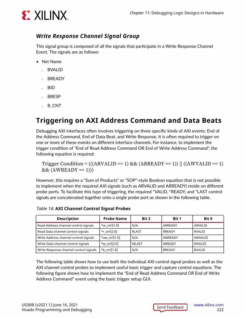
Write Response Channel Signal Group
This signal group is composed of all the signals that participate in a Write Response ChannelEvent. The signals are as follows:
• Net Name
○ BVALID
○ BREADY
○ BID
○ BRESP
○ B_CNT
Triggering on AXI Address Command and Data BeatsDebugging AXI interfaces often involves triggering on three specific kinds of AXI events: End ofthe Address Command, End of Data Beat, and Write Response. It is often required to trigger onone or more of these events on different interface channels. For instance, to implement thetrigger condition of "End of Read Address Command OR End of Write Address Command", thefollowing equation is required:
Trigger Condition = (((ARVALID == 1) && (ARREADY == 1)) || ((AWVALID == 1)&& (AWREADY == 1)))
However, this requires a "Sum of Products" or "SOP"-style Boolean equation that is not possibleto implement when the required AXI signals (such as ARVALID and ARREADY) reside on differentprobe ports. To facilitate this type of triggering, the required *VALID, *READY, and *LAST controlsignals are concatenated together onto a single probe port as shown in the following table.
Table 14: AXI Channel Control Signal Probes
Description Probe Name Bit 2 Bit 1 Bit 0Read Address channel control signals *ar_ctrl[1:0] N/A ARREADY ARVALID
Read Data channel control signals *r_ctrl[2:0] RLAST RREADY RVALID
Write Address channel control signals *aw_ctrl[1:0] N/A AWREADY AWVALID
Write Data channel control signals *w_ctrl[2:0] WLAST WREADY WVALID
Write Response channel control signals *b_ctrl[1:0] N/A BREADY BVALID
The following table shows how to use both the individual AXI control signal probes as well as theAXI channel control probes to implement useful basic trigger and capture control equations. Thefollowing figure shows how to implement the "End of Read Address Command OR End of WriteAddress Command" event using the basic trigger setup GUI.
Chapter 11: Debugging Logic Designs in Hardware
UG908 (v2021.1) June 16, 2021 www.xilinx.comVivado Programming and Debugging 222Send Feedback

Table 15: Trigger and/or Capture Control Event
AXI Event Individual AXI Control SignalsCombined AXI
Channel ControlProbe
End of the Read Address Command ((ARVALID == 1) && (ARREADY == 1)) (*ar_ctrl == 2'b11)
End of the Last Read Data Beat ((RVALID == 1) && (RREADY == 1) && (RLAST == 1)) (*r_ctrl == 3'b111)
End of the (Non-Last) Read DataBeat
((RVALID == 1) && (RREADY == 1) && (RLAST == 0)) (*r_ctrl == 3'b011)
End of the Write Address Command ((AWVALID == 1) && (AWREADY == 1)) (*aw_ctrl == 2'b11)
End of the Write Read Data Beat ((WVALID == 1) && (WREADY == 1) && (WLAST == 1)) (*w_ctrl == 3'b111)
End of the (Non-Last) Read DataBeat
((WVALID == 1) && (WREADY == 1) && (WLAST == 0)) (*w_ctrl == 3'b011)
Figure 144: Basic Trigger Setup for "End of Read Address Command OR End of WriteAddress Command" Event
Setting Up the VIO Core to Take aMeasurement
The VIO cores that you add to your design appear in the Hardware window under the targetdevice. If you do not see the VIO cores appear, right-click the device and select RefreshHardware. This re-scans the FPGA or ACAP and refreshes the Hardware window.
Note: If you still do not see the VIO core after programming and/or refreshing the FPGA or ACAP, check tomake sure the device was programmed with the appropriate .pdi file and check to make sure theimplemented design contains an VIO core. Also, check to make sure the appropriate .ltx probes file thatmatches the .bit file is associated with the device.
Click the VIO core (called hw_vio_1 in the following figure) to see its properties in the VIO CoreProperties window. By selecting the VIO core, you should also see the probes corresponding tothe VIO core in the Debug Probes window as well as the corresponding VIO Dashboard in theVivado IDE workspace (see the following figure).
Chapter 11: Debugging Logic Designs in Hardware
UG908 (v2021.1) June 16, 2021 www.xilinx.comVivado Programming and Debugging 223Send Feedback
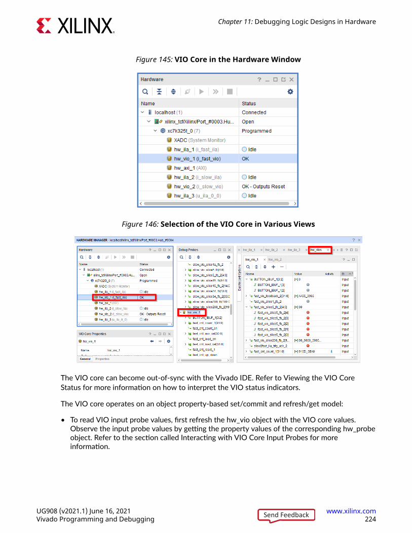
Figure 145: VIO Core in the Hardware Window
Figure 146: Selection of the VIO Core in Various Views
The VIO core can become out-of-sync with the Vivado IDE. Refer to Viewing the VIO CoreStatus for more information on how to interpret the VIO status indicators.
The VIO core operates on an object property-based set/commit and refresh/get model:
• To read VIO input probe values, first refresh the hw_vio object with the VIO core values.Observe the input probe values by getting the property values of the corresponding hw_probeobject. Refer to the section called Interacting with VIO Core Input Probes for moreinformation.
Chapter 11: Debugging Logic Designs in Hardware
UG908 (v2021.1) June 16, 2021 www.xilinx.comVivado Programming and Debugging 224Send Feedback
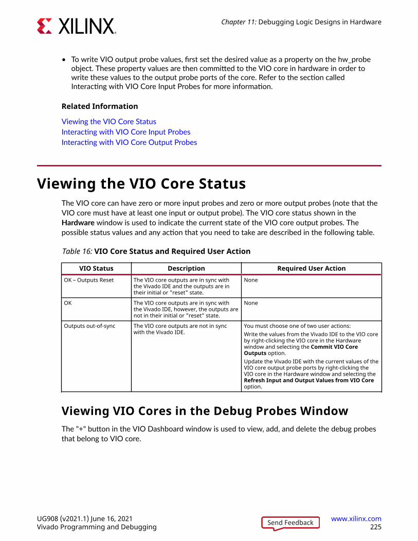
• To write VIO output probe values, first set the desired value as a property on the hw_probeobject. These property values are then committed to the VIO core in hardware in order towrite these values to the output probe ports of the core. Refer to the section calledInteracting with VIO Core Input Probes for more information.
Related Information
Viewing the VIO Core StatusInteracting with VIO Core Input ProbesInteracting with VIO Core Output Probes
Viewing the VIO Core StatusThe VIO core can have zero or more input probes and zero or more output probes (note that theVIO core must have at least one input or output probe). The VIO core status shown in theHardware window is used to indicate the current state of the VIO core output probes. Thepossible status values and any action that you need to take are described in the following table.
Table 16: VIO Core Status and Required User Action
VIO Status Description Required User ActionOK – Outputs Reset The VIO core outputs are in sync with
the Vivado IDE and the outputs are intheir initial or "reset" state.
None
OK The VIO core outputs are in sync withthe Vivado IDE, however, the outputs arenot in their initial or "reset” state.
None
Outputs out-of-sync The VIO core outputs are not in syncwith the Vivado IDE.
You must choose one of two user actions:Write the values from the Vivado IDE to the VIO coreby right-clicking the VIO core in the Hardwarewindow and selecting the Commit VIO CoreOutputs option.Update the Vivado IDE with the current values of theVIO core output probe ports by right-clicking theVIO core in the Hardware window and selecting theRefresh Input and Output Values from VIO Coreoption.
Viewing VIO Cores in the Debug Probes WindowThe "+" button in the VIO Dashboard window is used to view, add, and delete the debug probesthat belong to VIO core.
Chapter 11: Debugging Logic Designs in Hardware
UG908 (v2021.1) June 16, 2021 www.xilinx.comVivado Programming and Debugging 225Send Feedback
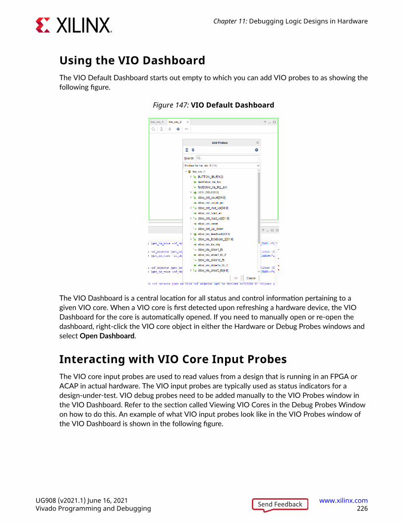
Using the VIO DashboardThe VIO Default Dashboard starts out empty to which you can add VIO probes to as showing thefollowing figure.
Figure 147: VIO Default Dashboard
The VIO Dashboard is a central location for all status and control information pertaining to agiven VIO core. When a VIO core is first detected upon refreshing a hardware device, the VIODashboard for the core is automatically opened. If you need to manually open or re-open thedashboard, right-click the VIO core object in either the Hardware or Debug Probes windows andselect Open Dashboard.
Interacting with VIO Core Input ProbesThe VIO core input probes are used to read values from a design that is running in an FPGA orACAP in actual hardware. The VIO input probes are typically used as status indicators for adesign-under-test. VIO debug probes need to be added manually to the VIO Probes window inthe VIO Dashboard. Refer to the section called Viewing VIO Cores in the Debug Probes Windowon how to do this. An example of what VIO input probes look like in the VIO Probes window ofthe VIO Dashboard is shown in the following figure.
Chapter 11: Debugging Logic Designs in Hardware
UG908 (v2021.1) June 16, 2021 www.xilinx.comVivado Programming and Debugging 226Send Feedback

Figure 148: Core Input Probes
Related Information
Viewing VIO Cores in the Debug Probes Window
Reading VIO Inputs Using the VIO Cores ViewThe VIO input probes can be viewed using the VIO Probes window of the VIO Dashboardwindow. Each input probe is viewed as a separate row in the table. The value of the VIO inputprobes are shown in the Value column of the table (see Interacting with VIO Core Input Probes).The VIO core input values are periodically updated based on the value of the refresh rate of theVIO core. You can set the refresh rate by changing the Refresh Rate (ms) in the VIO Propertieswindow or by running the following Tcl command:
set_property CORE_REFRESH_RATE_MS 1000 [get_hw_vios hw_vio_1]
Note: Setting the refresh rate to 0 causes all automatic refreshes from the VIO core to stop. Also note thatvery small refresh values may cause your Vivado IDE to become sluggish. Xilinx recommends a refresh rateof 500 ms or longer.
If you want to manually read a VIO input probe value, you can use Tcl commands to do so. Forinstance, if you wanted to refresh and get the value of the input probe called BUTTON_IBUF ofthe VIO core hw_vio_1, run the following Tcl commands:
refresh_hw_vio [get_hw_vios {hw_vio_1}]get_property INPUT_VALUE [get_hw_probes BUTTON_IBUF]
Related Information
Interacting with VIO Core Input Probes
Chapter 11: Debugging Logic Designs in Hardware
UG908 (v2021.1) June 16, 2021 www.xilinx.comVivado Programming and Debugging 227Send Feedback
Setting the VIO Input Display Type and RadixThe display type of VIO input probes can be set by right-clicking a VIO input probe in the VIOProbes window of the VIO Dashboard window and selecting:
• Text to display the input as a text field. This is the only display type for VIO input probevectors (more than one bit wide).
• LED to display the input as a graphical representation of a light-emitting diode (LED). Thisdisplay type is only applicable to VIO input probe scalars and individual elements of VIO inputprobe vectors. You can set the high and low values to one of four colors:
○ Gray (off)
○ Red
○ Green
○ Blue
When the display type of the VIO input probe is set to Text, you can change the radix byright-clicking a VIO input probe in the VIO Probes window of the VIO Dashboard window andselecting:
• Radix > Binary to change the radix to binary.
• Radix > Octal to change the radix to octal.
• Radix > Hex to change the radix to hexadecimal.
• Radix > Unsigned to change the radix to unsigned decimal.
• Radix > Signed to change the radix to signed decimal.
You can also set the radix of the VIO input probe using a Tcl command. For instance, to changethe radix of a VIO input probe called "BUTTON_IBUF", run the following Tcl command:
set_property INPUT_VALUE_RADIX HEX [get_hw_probes BUTTON_IBUF]
Observing and Controlling VIO Input ActivityIn addition to reading values from the VIO input probes, you can also monitor the activity of theVIO input probes. The activity detectors are used to indicate when the values on the VIO inputshave changed in between periodic updates to the Vivado IDE.
The VIO input probe activity values are shown as arrows in the activity column of the VIOProbes window of the VIO Dashboard window:
• An up arrow indicates that the input probe value has transitioned from a 0 to a 1 during theactivity persistence interval.
Chapter 11: Debugging Logic Designs in Hardware
UG908 (v2021.1) June 16, 2021 www.xilinx.comVivado Programming and Debugging 228Send Feedback
• A down arrow indicates that the input probe value has transitioned from a 1 to a 0 during theactivity persistence interval.
• A double-sided arrow indicates that the input probe value has transitioned from a 1 to a 0 andfrom a 0 to a 1 at least once during the activity persistence interval.
The persistence of how long the input activity status is displayed can be controlled by right-clicking a VIO input probe in the VIO Probes window of the VIO Dashboard window andselecting:
• Activity Persistence > Infinite to accumulate and retain the activity value until you reset it.
• Activity Persistence > Long (80 samples) to accumulate and retain the activity for a longerperiod of time.
• Activity Persistence > Short (8 samples) to accumulate and retain the activity for a shorterperiod of time.
You can also set the activity persistence using a Tcl command. For instance, to change the activitypersistence on the VIO input probe called BUTTON_IBUF to a long interval, run the following Tclcommand:
set_property ACTIVITY_PERSISTENCE LONG [get_hw_probes BUTTON_IBUF]
The activity for all input probes for a given core can be reset by right-clicking the VIO core in theHardware window and selecting Reset All Input Activity. You can also do this by running thefollowing Tcl command:
reset_hw_vio_activity [get_hw_vios {hw_vio_1}]
TIP: You can change the type, radix, and/or activity persistence of multiple scalar members of a VIO inputprobe vector by right-clicking the whole probe or multiple members of the probe, then making a menuchoice. The menu choice applies to all selected probe scalars.
Interacting with VIO Core Output ProbesThe VIO core output probes are used to write values to a design that is running in an FPGA orACAP in actual hardware. The VIO output probes are typically used as low-bandwidth controlsignals for a design-under-test. VIO debug probes need to be added manually to the VIO Probeswindow in the VIO Dashboard. Refer to the section called Viewing VIO Cores in the DebugProbes Window on how to do this. An example of what VIO output probes look like in the VIOProbes window of the VIO Dashboard is shown in the following figure.
Chapter 11: Debugging Logic Designs in Hardware
UG908 (v2021.1) June 16, 2021 www.xilinx.comVivado Programming and Debugging 229Send Feedback

Figure 149: VIO Outputs in the VIO Probes Window of the VIO Dashboard
Related Information
Viewing VIO Cores in the Debug Probes Window
Writing VIO Outputs Using the VIO Cores ViewThe VIO output probes can be set using the VIO Probes window of the VIO Dashboard window.Each output probe is viewed as a separate row in the table. The value of the VIO output probesare shown in the Value column of the table (see Interacting with VIO Core output Probes). TheVIO core output values are updated whenever a new value is entered into the Value column.Clicking on the Value column causes a pull-down dialog to appear. Type the desired value intothe Value text field and click OK.
You can also write out a new value to the VIO core using Tcl commands. For instance, if youwanted to write a binary value of "11111" to the VIO output probe called vio_slice5_fb_2whose radix is already set to BINARY, run the following Tcl commands:
set_property OUTPUT_VALUE 11111 [get_hw_probes vio_slice5_fb_2]commit_hw_vio [get_hw_probes {vio_slice5_fb_2}]
Related Information
Interacting with VIO Core Output Probes
Chapter 11: Debugging Logic Designs in Hardware
UG908 (v2021.1) June 16, 2021 www.xilinx.comVivado Programming and Debugging 230Send Feedback

Setting the VIO Output Display Type and RadixThe display type of VIO output probes can be set by right-clicking a VIO output probe in the VIOProbes window of the VIO Dashboard window and selecting:
• Text to display the output as a text field. This is the only display type for VIO input probevectors (more than one bit wide).
• Toggle Button to display the output as a graphical representation of a toggle button. Thisdisplay type is only applicable to VIO output probe scalars and individual elements of VIOinput probe vectors.
When the display type of the VIO output probe is set to "Text", you can change the radix byright-clicking a VIO output probe in the VIO Cores tabbed view of the Debug Probes windowand selecting:
• Radix → Binary to change the radix to binary.
• Radix → Octal to change the radix to octal.
• Radix → Hex to change the radix to hexadecimal.
• Radix → Unsigned to change the radix to unsigned decimal.
• Radix → Signed to change the radix to signed decimal.
You can also set the radix of the VIO output probe using a Tcl command. For instance, to changethe radix of a VIO output probe called “vio_slice5_fb_2” to hexadecimal, run the following Tclcommand:
set_property OUTPUT_VALUE_RADIX HEX [get_hw_probes vio_slice5_fb_2]
Resetting the VIO Core Output ValuesThe VIO v2.0 core has a feature that allows you to specify an initial value for each output probeport. You can reset the VIO core output probe ports to these initial values by right-clicking theVIO core in the Hardware window and selecting the Reset VIO Core Outputs option. You canalso reset the VIO core outputs using a Tcl command:
reset_hw_vio_outputs [get_hw_vios {hw_vio_1}]
Note: Resetting the VIO output probes to their initial values may cause the output probe values to becomeout-of-sync with the Vivado IDE. Refer to the section called Synchronizing the VIO Core Output Values tothe Vivado IDE on how to handle this situation.
Related Information
Synchronizing the VIO Core Output Values to the Vivado IDE
Chapter 11: Debugging Logic Designs in Hardware
UG908 (v2021.1) June 16, 2021 www.xilinx.comVivado Programming and Debugging 231Send Feedback
Synchronizing the VIO Core Output Values to theVivado IDEThe output probes of a VIO core can become out-of-sync with the Vivado IDE after resetting theVIO outputs, re-programming the FPGA or ACAP, or by another Vivado tool instance settingoutput values before the current instance has started. In any case, if the VIO status indicates"Outputs out-of-sync", you need to take one of two actions:
• Write the values from the Vivado IDE to the VIO core by right-clicking the VIO core in theHardware window and selecting the Commit VIO Core Outputs option. You can also do thisrunning a Tcl command:
commit_hw_vio [get_hw_vios {hw_vio_1}]
• Update the Vivado IDE with the current values of the VIO core output probe ports by right-clicking the VIO core in the Hardware window and selecting the Refresh Input and OutputValues from VIO Core option. You can also do this running a Tcl command:
refresh_hw_vio -update_output_values 1 [get_hw_vios {hw_vio_1}]
Hardware System Communication Using theJTAG-to-AXI Master Debug Core
The JTAG-to-AXI Master debug core is a customizable core that can generate the AXItransactions and drive the AXI signals internal to an FPGA at run time. The core supports allmemory mapped AXI and AXI-Lite interfaces and can support 32- or 64-bit wide data interfaces.
The JTAG-to-AXI Master (JTAG-AXI) cores that you add to your design appear in the Hardwarewindow under the target device. If you do not see the JTAG-AXI cores appear, right-click thedevice and select Refresh Hardware. This re-scans the FPGA device and refreshes the Hardwarewindow.
Note: If you still do not see the ILA core after programming and/or refreshing the FPGA device, check tomake sure the device was programmed with the appropriate .bit file and check to make sure theimplemented design contains an ILA core.
Click to select the JTAG-AXI core (called hw_axi_1 in the following figure) to see its properties inthe AXI Core Properties window.
Chapter 11: Debugging Logic Designs in Hardware
UG908 (v2021.1) June 16, 2021 www.xilinx.comVivado Programming and Debugging 232Send Feedback
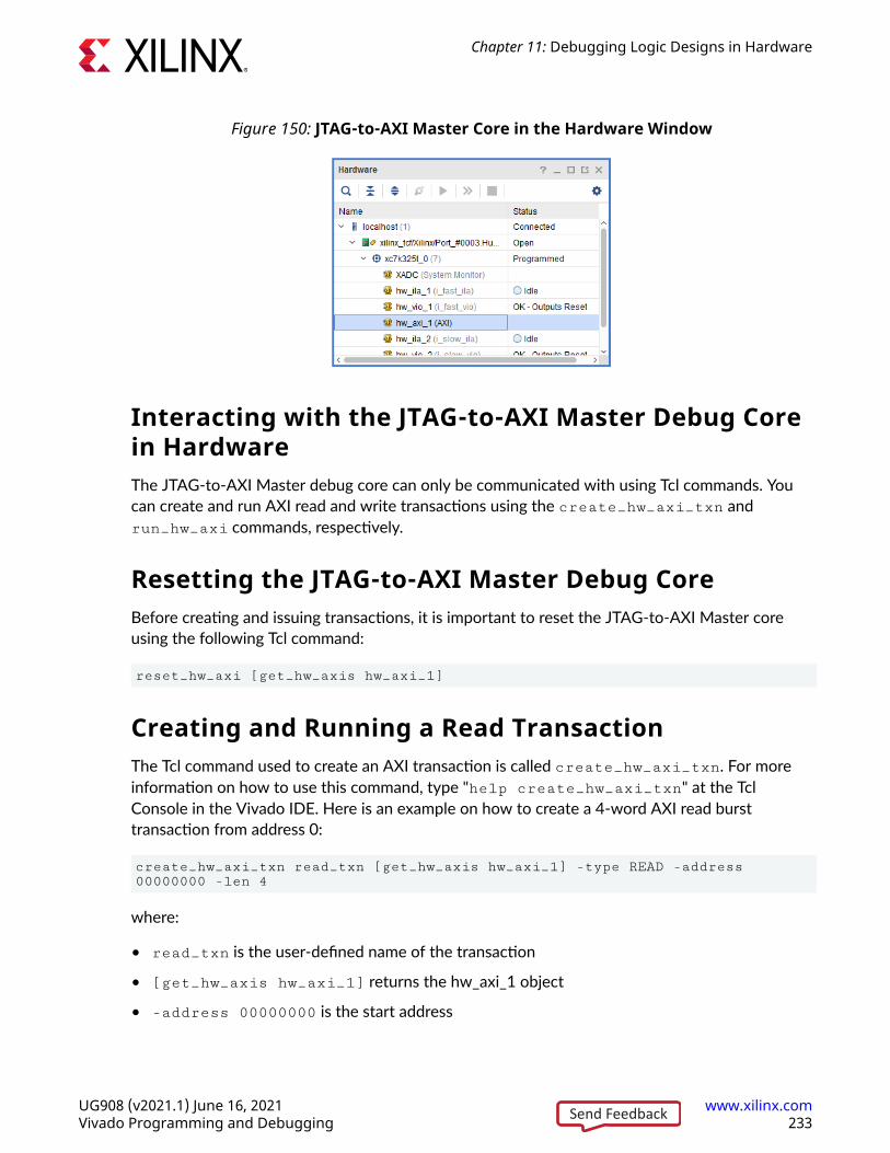
Figure 150: JTAG-to-AXI Master Core in the Hardware Window
Interacting with the JTAG-to-AXI Master Debug Corein HardwareThe JTAG-to-AXI Master debug core can only be communicated with using Tcl commands. Youcan create and run AXI read and write transactions using the create_hw_axi_txn andrun_hw_axi commands, respectively.
Resetting the JTAG-to-AXI Master Debug CoreBefore creating and issuing transactions, it is important to reset the JTAG-to-AXI Master coreusing the following Tcl command:
reset_hw_axi [get_hw_axis hw_axi_1]
Creating and Running a Read TransactionThe Tcl command used to create an AXI transaction is called create_hw_axi_txn. For moreinformation on how to use this command, type "help create_hw_axi_txn" at the TclConsole in the Vivado IDE. Here is an example on how to create a 4-word AXI read bursttransaction from address 0:
create_hw_axi_txn read_txn [get_hw_axis hw_axi_1] -type READ -address 00000000 -len 4
where:
• read_txn is the user-defined name of the transaction
• [get_hw_axis hw_axi_1] returns the hw_axi_1 object
• -address 00000000 is the start address
Chapter 11: Debugging Logic Designs in Hardware
UG908 (v2021.1) June 16, 2021 www.xilinx.comVivado Programming and Debugging 233Send Feedback
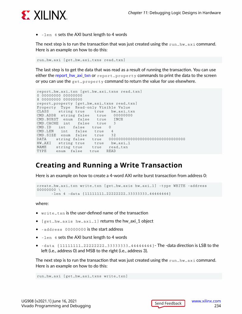
• -len 4 sets the AXI burst length to 4 words
The next step is to run the transaction that was just created using the run_hw_axi command.Here is an example on how to do this:
run_hw_axi [get_hw_axi_txns read_txn]
The last step is to get the data that was read as a result of running the transaction. You can useeither the report_hw_axi_txn or report_property commands to print the data to the screenor you can use the get_property command to return the value for use elsewhere.
report_hw_axi_txn [get_hw_axi_txns read_txn]0 00000000 000000008 00000000 00000000report_property [get_hw_axi_txns read_txn]Property Type Read-only Visible ValueCLASS string true true hw_axi_txnCMD.ADDR string false true 00000000CMD.BURST enum false true INCRCMD.CACHE int false true 3CMD.ID int false true 0CMD.LEN int false true 4CMD.SIZE enum false true 32DATA string false true 00000000000000000000000000000000HW_AXI string true true hw_axi_1NAME string true true read_txnTYPE enum false true READ
Creating and Running a Write TransactionHere is an example on how to create a 4-word AXI write burst transaction from address 0:
create_hw_axi_txn write_txn [get_hw_axis hw_axi_1] -type WRITE -address 00000000 \ -len 4 -data {11111111_22222222_33333333_44444444}
where:
• write_txn is the user-defined name of the transaction
• [get_hw_axis hw_axi_1] returns the hw_axi_1 object
• -address 00000000 is the start address
• -len 4 sets the AXI burst length to 4 words
• -data {11111111_22222222_33333333_44444444}- The -data direction is LSB to theleft (i.e., address 0) and MSB to the right (i.e., address 3).
The next step is to run the transaction that was just created using the run_hw_axi command.Here is an example on how to do this:
run_hw_axi [get_hw_axi_txns write_txn]
Chapter 11: Debugging Logic Designs in Hardware
UG908 (v2021.1) June 16, 2021 www.xilinx.comVivado Programming and Debugging 234Send Feedback
IMPORTANT! If you reprogram the device, all the existing jtag_axi transactions will be deleted. You mayneed to recreate these transactions again.
TIP: The -queue optional argument to the run_hw_axi Tcl command allows you to specify hw_axitransactions in queue mode. Queued operation allows up to 16 read and 16 write transactions to bequeued in the JTAG to AXI Master FIFO and issued back-to-back for low latency and higher performancebetween the transactions. Non-queued transactions are simply run as submitted.
Using Vivado Logic Analyzer in a LabEnvironment
The Vivado logic analyzer feature is integrated into the Vivado IDE and Vivado Lab Edition. Touse Vivado logic analyzer feature to debug a design that is running on a target board that is in alab environment, you need to do one of three things:
• Install and run the Vivado Lab Edition on your lab machine. For more details refer to VivadooLab Edition of this user guide.
• Install and run the full Vivado IDE on your lab machine.
• Install latest version of the Vivado Design Suite or Vivado Hardware Server (Standalone) onyour remote lab machine, and use the Vivado logic analyzer feature on your local machine toconnect to a remote instance of the Vivado Hardware Server (hw_server).
Related Information
Vivado Lab Edition
Connecting to a Remote hw_server Running on a LabMachineIf you have a network connection to your lab machine, you can also connect to the target boardby connecting to a Hardware Server that is running on that remote lab machine. Here are thesteps to using the Vivado logic analyzer feature to connect to a Vivado Hardware Server(hw_server.bat on Windows platforms or hw_server on Linux platforms) that is running onthe lab machine:
1. Install the latest version of the Vivado Design Suite or Vivado Hardware Server (Standalone)on the lab machine.
Chapter 11: Debugging Logic Designs in Hardware
UG908 (v2021.1) June 16, 2021 www.xilinx.comVivado Programming and Debugging 235Send Feedback
IMPORTANT! You do NOT need to install the full Vivado Design Suite or Vivado Lab Edition on thelab machine to only use the remote hardware server feature. However, if you do want to use theVivado Hardware Manager features (such as the Vivado logic analyzer or Vivado serial I/O analyzer)on the lab machine, then you will need to install the Vivado Lab Edition on the lab machine. Also, youdo NOT need any software licenses to run the Hardware Server, any of the Hardware Managerfeatures of the Vivado Design Suite, or the Vivado Lab Edition.
2. Start up the hw_server application on the remote lab machine. Assuming you installed theVivado Hardware Server (Standalone) to the default location and your lab machine is a 64-bitWindows machine, here is the command line:
C:\Xilinx\VivadoHWSRV\vivado_release.version\bin\hw_server.bat
3. Start Vivado IDE in GUI mode on a different machine than your lab machine.
4. Follow the steps in the Connecting to the Hardware Target and Programming the Devicesection to open a connection to the target board that is connected to your lab machine.However, instead of connecting to a Vivado CSE server running on localhost, use the hostname of your lab machine.
5. Follow the steps in the Setting up the ILA Core to Take a Measurement section and beyond todebug your design in hardware.
Related Information
Connecting to the Hardware Target and Programming the DeviceSetting Up the ILA Core to Take a Measurement
Description of Hardware Manager Tcl Objectsand Commands
You can use Tcl commands to interact with your hardware under test. The hardware is organizedin a set of hierarchical first class Tcl objects (see the following table).
Table 17: Hardware Manager Tcl Objects
Tcl Object Descriptionhw_server Object referring to hardware server. Each hw_server can have one or more hw_target
objects associated with it.
hw_target Object referring to JTAG cable or board. Each hw_target can have one or more hw_deviceobjects associated with it.
hw_device Object referring to a device in the JTAG chain, including Xilinx FPGAs or ACAPs. Eachhw_device can have one or more hw_ila objects associated with it.
hw_ila Object referring to an ILA core in the Xilinx FPGA or ACAP. Each hw_ila object can haveonly one hw_ila_data object associated with it. Each hw_ila object can have one or morehw_probe objects associated with it.
Chapter 11: Debugging Logic Designs in Hardware
UG908 (v2021.1) June 16, 2021 www.xilinx.comVivado Programming and Debugging 236Send Feedback
Table 17: Hardware Manager Tcl Objects (cont'd)
Tcl Object Descriptionhw_ila_data Object referring to data uploaded from an ILA debug core.
hw_probe Object referring to the probe input of an ILA debug core.
hw_vio Object referring to a VIO core in the Xilinx FPGA or ACAP.
For more information about the Hardware Manager commands, run the help -categoryhardware Tcl command in the Tcl Console.
Description of hw_server Tcl CommandsThe following table contains descriptions of all Tcl commands used to interact with hardwareservers.
Table 18: Descriptions of hw_server Tcl Commands
Tcl Command Descriptionconnect_hw_server Open a connection to a hardware server.
current_hw_server Get or set the current hardware server.
disconnect_hw_server Close a connection to a hardware server.
get_hw_servers Get list of hardware server names for the hardware servers.
refresh_hw_server Refresh a connection to a hardware server.
Description of hw_target Tcl CommandsThe following table contains descriptions of all Tcl commands used to interact with hardwaretargets.
Table 19: Descriptions of hw_target Tcl Commands
Tcl Command Descriptionclose_hw_target Close a hardware target.
current_hw_target Get or set the current hardware target.
get_hw_targets Get list of hardware targets for the hardware servers.
open_hw_target Open a connection to a hardware target on the hardware server.
refresh_hw_target Refresh a connection to a hardware target.
Description of hw_device Tcl CommandsThe following table contains descriptions of hw_device Tcl Commands contains descriptions of allTcl commands used to interact with hardware devices.
Chapter 11: Debugging Logic Designs in Hardware
UG908 (v2021.1) June 16, 2021 www.xilinx.comVivado Programming and Debugging 237Send Feedback
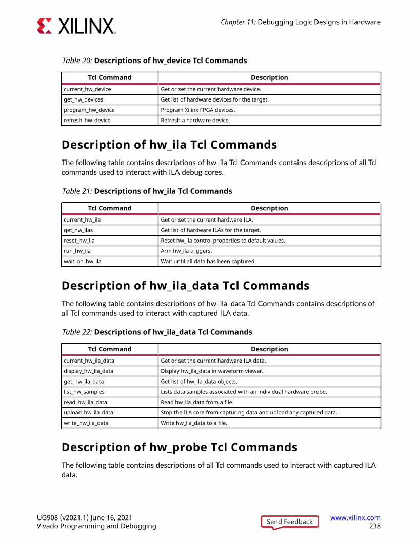
Table 20: Descriptions of hw_device Tcl Commands
Tcl Command Descriptioncurrent_hw_device Get or set the current hardware device.
get_hw_devices Get list of hardware devices for the target.
program_hw_device Program Xilinx FPGA devices.
refresh_hw_device Refresh a hardware device.
Description of hw_ila Tcl CommandsThe following table contains descriptions of hw_ila Tcl Commands contains descriptions of all Tclcommands used to interact with ILA debug cores.
Table 21: Descriptions of hw_ila Tcl Commands
Tcl Command Descriptioncurrent_hw_ila Get or set the current hardware ILA.
get_hw_ilas Get list of hardware ILAs for the target.
reset_hw_ila Reset hw_ila control properties to default values.
run_hw_ila Arm hw_ila triggers.
wait_on_hw_ila Wait until all data has been captured.
Description of hw_ila_data Tcl CommandsThe following table contains descriptions of hw_ila_data Tcl Commands contains descriptions ofall Tcl commands used to interact with captured ILA data.
Table 22: Descriptions of hw_ila_data Tcl Commands
Tcl Command Descriptioncurrent_hw_ila_data Get or set the current hardware ILA data.
display_hw_ila_data Display hw_ila_data in waveform viewer.
get_hw_ila_data Get list of hw_ila_data objects.
list_hw_samples Lists data samples associated with an individual hardware probe.
read_hw_ila_data Read hw_ila_data from a file.
upload_hw_ila_data Stop the ILA core from capturing data and upload any captured data.
write_hw_ila_data Write hw_ila_data to a file.
Description of hw_probe Tcl CommandsThe following table contains descriptions of all Tcl commands used to interact with captured ILAdata.
Chapter 11: Debugging Logic Designs in Hardware
UG908 (v2021.1) June 16, 2021 www.xilinx.comVivado Programming and Debugging 238Send Feedback
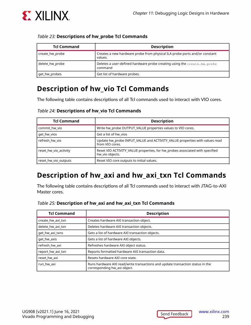
Table 23: Descriptions of hw_probe Tcl Commands
Tcl Command Descriptioncreate_hw_probe Creates a new hardware probe from physical ILA probe ports and/or constant
values.
delete_hw_probe Deletes a user-defined hardware probe creating using the create_hw_probecommand
get_hw_probes Get list of hardware probes.
Description of hw_vio Tcl CommandsThe following table contains descriptions of all Tcl commands used to interact with VIO cores.
Table 24: Descriptions of hw_vio Tcl Commands
Tcl Command Descriptioncommit_hw_vio Write hw_probe OUTPUT_VALUE properties values to VIO cores.
get_hw_vios Get a list of hw_vios
refresh_hw_vio Update hw_probe INPUT_VALUE and ACTIVITY_VALUE properties with values readfrom VIO cores.
reset_hw_vio_activity Reset VIO ACTIVITY_VALUE properties, for hw_probes associated with specifiedhw_vio objects.
reset_hw_vio_outputs Reset VIO core outputs to initial values.
Description of hw_axi and hw_axi_txn Tcl CommandsThe following table contains descriptions of all Tcl commands used to interact with JTAG-to-AXIMaster cores.
Table 25: Description of hw_axi and hw_axi_txn Tcl Commands
Tcl Command Descriptioncreate_hw_axi_txn Creates hardware AXI transaction object.
delete_hw_axi_txn Deletes hardware AXI transaction objects.
get_hw_axi_txns Gets a list of hardware AXI transaction objects.
get_hw_axis Gets a list of hardware AXI objects.
refresh_hw_axi Refreshes hardware AXI object status.
report_hw_axi_txn Reports formatted hardware AXI transaction data.
reset_hw_axi Resets hardware AXI core state.
run_hw_axi Runs hardware AXI read/write transactions and update transaction status in thecorresponding hw_axi object.
Chapter 11: Debugging Logic Designs in Hardware
UG908 (v2021.1) June 16, 2021 www.xilinx.comVivado Programming and Debugging 239Send Feedback
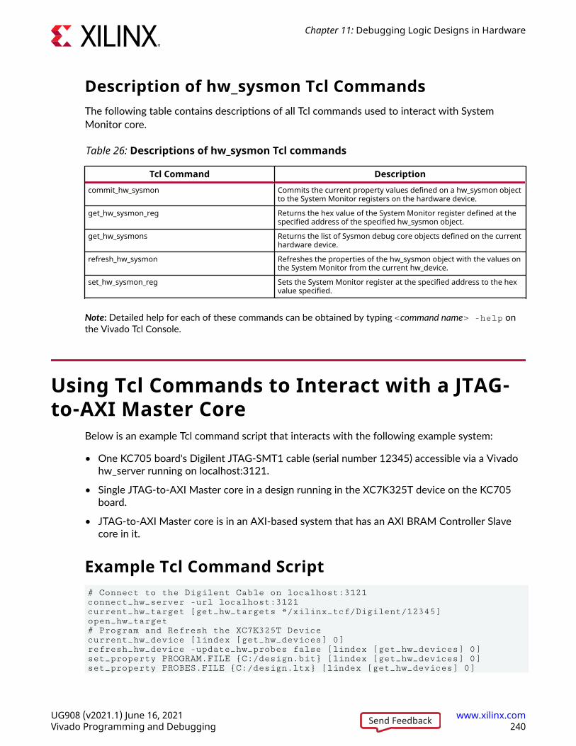
Description of hw_sysmon Tcl CommandsThe following table contains descriptions of all Tcl commands used to interact with SystemMonitor core.
Table 26: Descriptions of hw_sysmon Tcl commands
Tcl Command Descriptioncommit_hw_sysmon Commits the current property values defined on a hw_sysmon object
to the System Monitor registers on the hardware device.
get_hw_sysmon_reg Returns the hex value of the System Monitor register defined at thespecified address of the specified hw_sysmon object.
get_hw_sysmons Returns the list of Sysmon debug core objects defined on the currenthardware device.
refresh_hw_sysmon Refreshes the properties of the hw_sysmon object with the values onthe System Monitor from the current hw_device.
set_hw_sysmon_reg Sets the System Monitor register at the specified address to the hexvalue specified.
Note: Detailed help for each of these commands can be obtained by typing <command name> -help onthe Vivado Tcl Console.
Using Tcl Commands to Interact with a JTAG-to-AXI Master Core
Below is an example Tcl command script that interacts with the following example system:
• One KC705 board's Digilent JTAG-SMT1 cable (serial number 12345) accessible via a Vivadohw_server running on localhost:3121.
• Single JTAG-to-AXI Master core in a design running in the XC7K325T device on the KC705board.
• JTAG-to-AXI Master core is in an AXI-based system that has an AXI BRAM Controller Slavecore in it.
Example Tcl Command Script# Connect to the Digilent Cable on localhost:3121 connect_hw_server -url localhost:3121 current_hw_target [get_hw_targets */xilinx_tcf/Digilent/12345]open_hw_target# Program and Refresh the XC7K325T Devicecurrent_hw_device [lindex [get_hw_devices] 0]refresh_hw_device -update_hw_probes false [lindex [get_hw_devices] 0]set_property PROGRAM.FILE {C:/design.bit} [lindex [get_hw_devices] 0]set_property PROBES.FILE {C:/design.ltx} [lindex [get_hw_devices] 0]
Chapter 11: Debugging Logic Designs in Hardware
UG908 (v2021.1) June 16, 2021 www.xilinx.comVivado Programming and Debugging 240Send Feedback
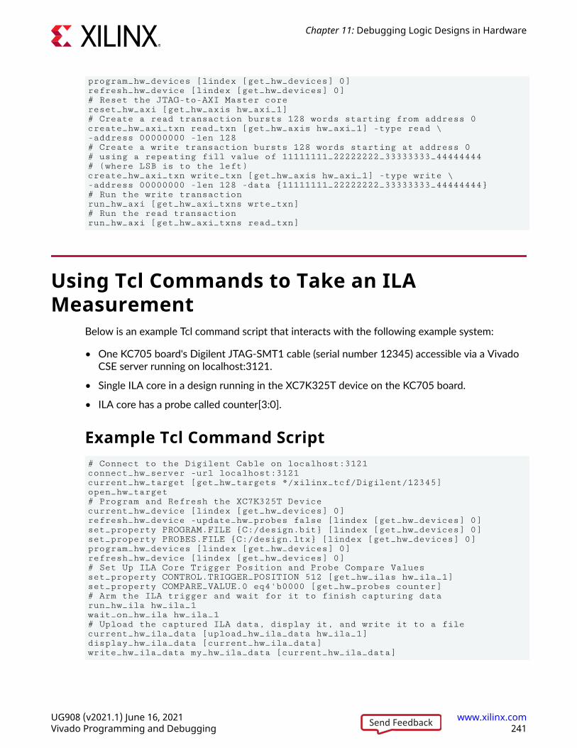
program_hw_devices [lindex [get_hw_devices] 0]refresh_hw_device [lindex [get_hw_devices] 0]# Reset the JTAG-to-AXI Master corereset_hw_axi [get_hw_axis hw_axi_1]# Create a read transaction bursts 128 words starting from address 0create_hw_axi_txn read_txn [get_hw_axis hw_axi_1] -type read \-address 00000000 -len 128# Create a write transaction bursts 128 words starting at address 0# using a repeating fill value of 11111111_22222222_33333333_44444444# (where LSB is to the left)create_hw_axi_txn write_txn [get_hw_axis hw_axi_1] -type write \-address 00000000 -len 128 -data {11111111_22222222_33333333_44444444}# Run the write transactionrun_hw_axi [get_hw_axi_txns wrte_txn]# Run the read transactionrun_hw_axi [get_hw_axi_txns read_txn]
Using Tcl Commands to Take an ILAMeasurement
Below is an example Tcl command script that interacts with the following example system:
• One KC705 board's Digilent JTAG-SMT1 cable (serial number 12345) accessible via a VivadoCSE server running on localhost:3121.
• Single ILA core in a design running in the XC7K325T device on the KC705 board.
• ILA core has a probe called counter[3:0].
Example Tcl Command Script# Connect to the Digilent Cable on localhost:3121connect_hw_server -url localhost:3121current_hw_target [get_hw_targets */xilinx_tcf/Digilent/12345]open_hw_target# Program and Refresh the XC7K325T Devicecurrent_hw_device [lindex [get_hw_devices] 0]refresh_hw_device -update_hw_probes false [lindex [get_hw_devices] 0]set_property PROGRAM.FILE {C:/design.bit} [lindex [get_hw_devices] 0]set_property PROBES.FILE {C:/design.ltx} [lindex [get_hw_devices] 0]program_hw_devices [lindex [get_hw_devices] 0]refresh_hw_device [lindex [get_hw_devices] 0]# Set Up ILA Core Trigger Position and Probe Compare Valuesset_property CONTROL.TRIGGER_POSITION 512 [get_hw_ilas hw_ila_1]set_property COMPARE_VALUE.0 eq4'b0000 [get_hw_probes counter]# Arm the ILA trigger and wait for it to finish capturing datarun_hw_ila hw_ila_1wait_on_hw_ila hw_ila_1# Upload the captured ILA data, display it, and write it to a filecurrent_hw_ila_data [upload_hw_ila_data hw_ila_1]display_hw_ila_data [current_hw_ila_data]write_hw_ila_data my_hw_ila_data [current_hw_ila_data]
Chapter 11: Debugging Logic Designs in Hardware
UG908 (v2021.1) June 16, 2021 www.xilinx.comVivado Programming and Debugging 241Send Feedback
Trigger At StartupThe Trigger at Startup feature is used to configure the trigger settings of an ILA core in adesign .bit file so that it is pre-armed to trigger immediately after device startup. You do thisby taking the various trigger settings that ordinarily get applied to an ILA core running in a designin hardware, and applying them to the ILA core in the implemented design.
IMPORTANT! The following process for using Trigger at Startup assumes that you are have a valid ILAdesign working in hardware, and that the ILA core has NOT been flattened during the synthesis flow.
To use the Trigger at Startup feature perform the following steps:
1. Run through the first pass of the ILA flow as usual to set up the trigger condition.
a. Open the target, configure the device, and bring up the ILA Dashboard.
b. Enter the trigger equations for the ILA core in the ILA Dashboard.
2. From the Vivado Tcl command line, export the trigger register map file for the ILA core. Thisfile contains all of the register settings to "stamp" back on to the implemented netlist. Theoutput from this is a single file.
% run_hw_ila -file ila_trig.tas [get_hw_ilas hw_ila_1]
3. Go back and open the previously implemented routed design in Vivado IDE. There are twoways to do this depending on your project flow.
a. Project Mode: Use the Flow Navigator to open the implemented design.
b. Non-Project Mode: Open your routed checkpoint: %open_checkpoint <file>.dcp
4. At the Implemented Design Tcl Console, apply the trigger settings to the current design inmemory, which is your routed netlist.
%apply_hw_ila_trigger ila_trig.tas
Note: If you see an ERROR indicating that the ILA core has been flattened during synthesis, you willneed to regenerate your design and force synthesis to preserve hierarchy for the ILA core. Ensure thatyou are have a valid ILA design working in hardware, and that the ILA core has NOT been flattenedduring the synthesis flow.
5. At the Implemented Design Tcl Console, write the bitstream with Trigger at Startup settings.
IMPORTANT! To pick up the routed design changes do this at the Tcl command console only: write_bitstream trig_at_startup.bit
6. Go back to the Hardware Manager and reconfigure with the new .bit file that yougenerated in the previous step. You will have to set the property for the updated .bit filelocation either through the GUI or through a Tcl command. Make sure you set the new .bitfile as the one to use for configuration in the hardware tool.
a. Select the device in the hardware tree.
Chapter 11: Debugging Logic Designs in Hardware
UG908 (v2021.1) June 16, 2021 www.xilinx.comVivado Programming and Debugging 242Send Feedback
b. Assign the .bit file generated in step 5.
7. Program the device using the new .bit file.
Once programmed, the new ILA core should immediately arm at startup. You should see anindication in the Trigger Capture Status for the ILA core. If trigger or capture events haveoccurred, the ILA core is now populated with captured data samples.
Memory Calibration DebugMemory Interface IPs in Vivado support calibration debug. They store useful core configuration,calibration, and data window information that is accessible in the Vivado Hardware Manager. TheMemory Calibration Debug can be used at any point to read out this information and getvaluable statistics and feedback from the memory interface IPs. The information can be viewedthrough a Memory Calibration Debug GUI in the Vivado Hardware Manager or through availableMemory Calibration Debug Tcl commands.
Memory Calibration Debug GUI UsageUpon configuring the device, the memory interfaces are visible in the Vivado Hardware Manager.
Memory calibration content are shown in a a debug interface that can be used to very quicklyidentify calibration status, and read and write window margin. This debug interface is alwaysincluded in the generated Memory Interface (UltraScale, and UltraScale+) designs.
Figure 151: Memory Calibration Debug Interface
Chapter 11: Debugging Logic Designs in Hardware
UG908 (v2021.1) June 16, 2021 www.xilinx.comVivado Programming and Debugging 243Send Feedback
Memory Calibration Debug Tcl UsageUse the following Tcl commands in the Vivado Tcl Console when connected to the hardware inVivado Hardware Manager to output all memory calibration debug content that is displayed inthe Vivado IDE.
• get_hw_migs
○ Displays what memory interfaces exist in the design.
• refresh_hw_mig [lindex [get_hw_migs] 0]
○ Refreshes only the memory interfaces denoted by index (index begins with 0).
• report_propery[lindex [get_hw_migs] 0]
○ Reports all of the parameters available for the memory interface.
○ Where 0 is the index of the memory interface to be reported (index begins with 0).
For more specific details see the UltraScale or 7 Series Memory Calibration debug commandsin the following documents:
• Xilinx Answer 43879, MIG 7 Series DDR3/DDR2 - Hardware Debug Guide.
• UltraScale Architecture-Based FPGAs Memory IP LogiCORE IP Product Guide (PG150)
DDRMC Calibration Debug GUI UsageThe DDRMC is one of the many integrated blocks included in the Versal architecture. Uponconfiguring the Versal device, both the enabled and disabled memory interfaces are visible in theVivado Hardware Manager.
Chapter 11: Debugging Logic Designs in Hardware
UG908 (v2021.1) June 16, 2021 www.xilinx.comVivado Programming and Debugging 244Send Feedback
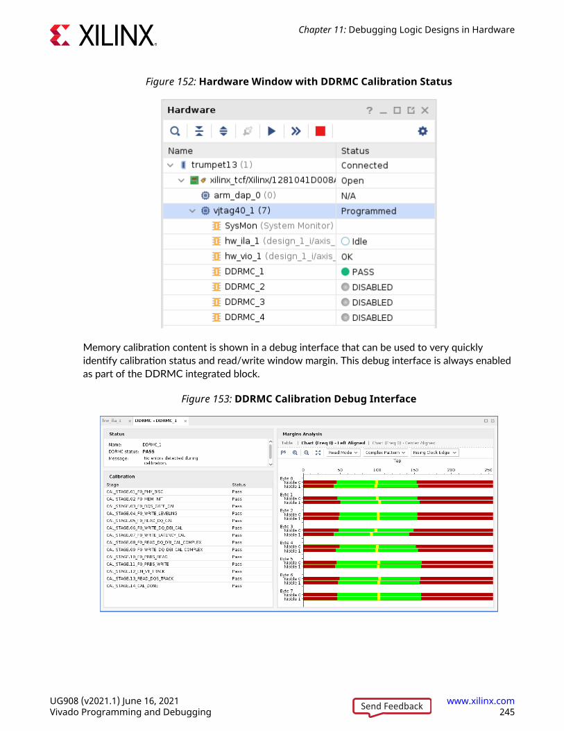
Figure 152: Hardware Window with DDRMC Calibration Status
Memory calibration content is shown in a debug interface that can be used to very quicklyidentify calibration status and read/write window margin. This debug interface is always enabledas part of the DDRMC integrated block.
Figure 153: DDRMC Calibration Debug Interface
Chapter 11: Debugging Logic Designs in Hardware
UG908 (v2021.1) June 16, 2021 www.xilinx.comVivado Programming and Debugging 245Send Feedback
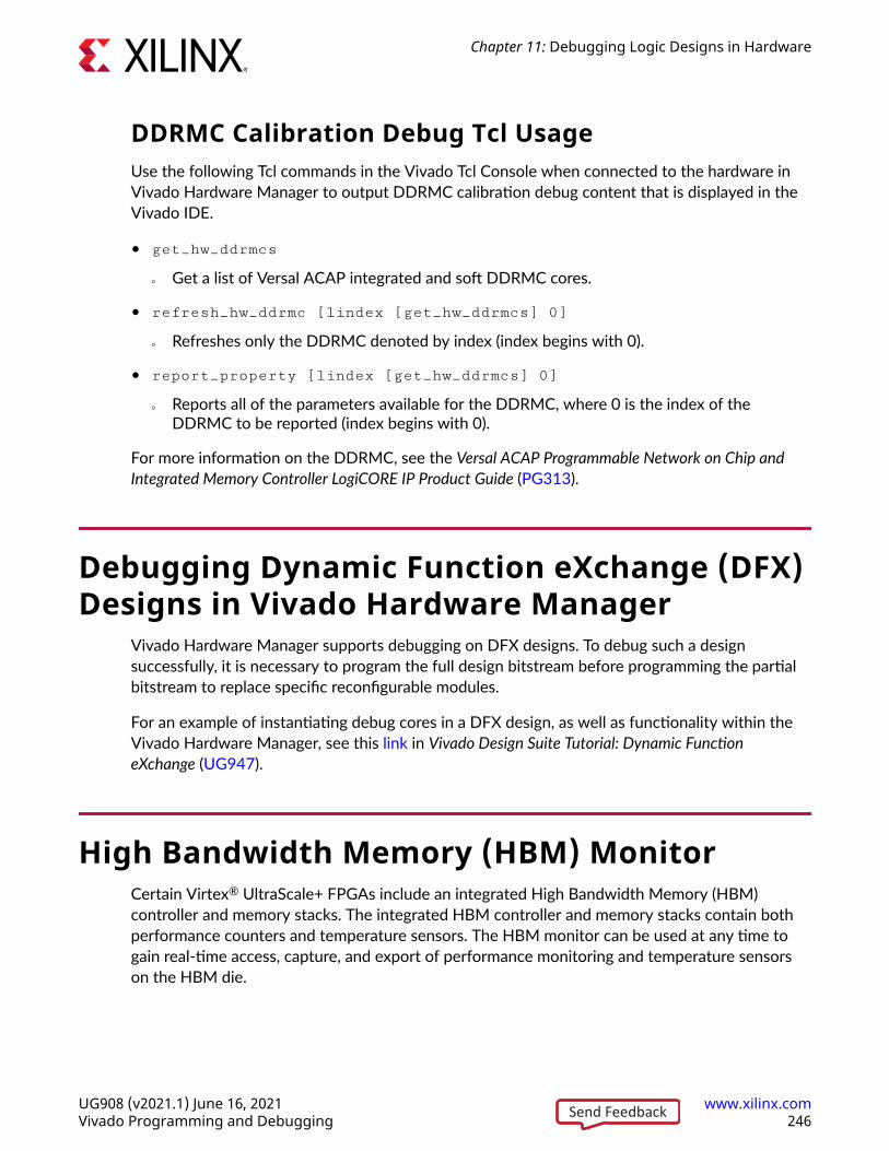
DDRMC Calibration Debug Tcl UsageUse the following Tcl commands in the Vivado Tcl Console when connected to the hardware inVivado Hardware Manager to output DDRMC calibration debug content that is displayed in theVivado IDE.
• get_hw_ddrmcs
○ Get a list of Versal ACAP integrated and soft DDRMC cores.
• refresh_hw_ddrmc [lindex [get_hw_ddrmcs] 0]
○ Refreshes only the DDRMC denoted by index (index begins with 0).
• report_property [lindex [get_hw_ddrmcs] 0]
○ Reports all of the parameters available for the DDRMC, where 0 is the index of theDDRMC to be reported (index begins with 0).
For more information on the DDRMC, see the Versal ACAP Programmable Network on Chip andIntegrated Memory Controller LogiCORE IP Product Guide (PG313).
Debugging Dynamic Function eXchange (DFX)Designs in Vivado Hardware Manager
Vivado Hardware Manager supports debugging on DFX designs. To debug such a designsuccessfully, it is necessary to program the full design bitstream before programming the partialbitstream to replace specific reconfigurable modules.
For an example of instantiating debug cores in a DFX design, as well as functionality within theVivado Hardware Manager, see this link in Vivado Design Suite Tutorial: Dynamic FunctioneXchange (UG947).
High Bandwidth Memory (HBM) MonitorCertain Virtex® UltraScale+ FPGAs include an integrated High Bandwidth Memory (HBM)controller and memory stacks. The integrated HBM controller and memory stacks contain bothperformance counters and temperature sensors. The HBM monitor can be used at any time togain real-time access, capture, and export of performance monitoring and temperature sensorson the HBM die.
Chapter 11: Debugging Logic Designs in Hardware
UG908 (v2021.1) June 16, 2021 www.xilinx.comVivado Programming and Debugging 246Send Feedback
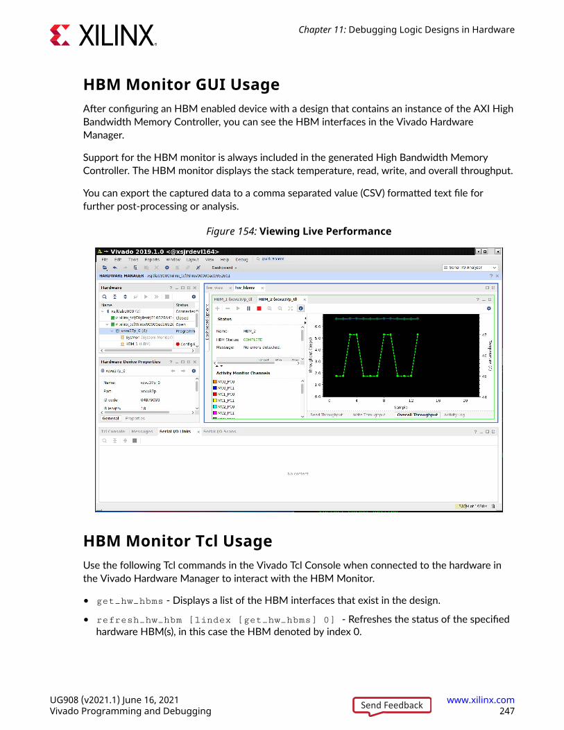
HBM Monitor GUI UsageAfter configuring an HBM enabled device with a design that contains an instance of the AXI HighBandwidth Memory Controller, you can see the HBM interfaces in the Vivado HardwareManager.
Support for the HBM monitor is always included in the generated High Bandwidth MemoryController. The HBM monitor displays the stack temperature, read, write, and overall throughput.
You can export the captured data to a comma separated value (CSV) formatted text file forfurther post-processing or analysis.
Figure 154: Viewing Live Performance
HBM Monitor Tcl UsageUse the following Tcl commands in the Vivado Tcl Console when connected to the hardware inthe Vivado Hardware Manager to interact with the HBM Monitor.
• get_hw_hbms - Displays a list of the HBM interfaces that exist in the design.
• refresh_hw_hbm [lindex [get_hw_hbms] 0] - Refreshes the status of the specifiedhardware HBM(s), in this case the HBM denoted by index 0.
Chapter 11: Debugging Logic Designs in Hardware
UG908 (v2021.1) June 16, 2021 www.xilinx.comVivado Programming and Debugging 247Send Feedback
• report_property [lindex [get_hw_hbms] 0] - Reports all the parameters availablefor the HBM interface specified, in this case for the HBM interface denoted by index 0.
• run_hw_hbm_amon [lindex [get_hw_hbms] 0] - Enables the activity monitor runs forthe specified hardware HBM(s).
• stop_hw_hbm_amon [lindex [get_hw_hbms] 0] - Disables the Activity Monitor runsfor the specified hardware HBM(s).
More specific details and examples can be found in Appendix D of AXI High Bandwidth ControllerLogiCORE IP Product Guide (PG276).
PCI Express Link DebugThe Versal PCI Express® Integrated Block in Vivado supports link debug. If enabled, the core willstore the Link Training and Status State Machine (LTSSM) state transitions which is accessible inthe Vivado Hardware Manager.
Enabling PCI Express Link DebugTo use PCI Express Link Debug, it must be enabled in the Versal PCI Express Integrated Block IP.
To enable the PCI Express Link Debug feature:
1. Invoke the Versal PCI Express Integrated Block IP configuration GUI.
2. Under the Basic tab, change the Mode to Advanced.
3. Under Other Settings, check PCIe-Link Debug.
Chapter 11: Debugging Logic Designs in Hardware
UG908 (v2021.1) June 16, 2021 www.xilinx.comVivado Programming and Debugging 248Send Feedback
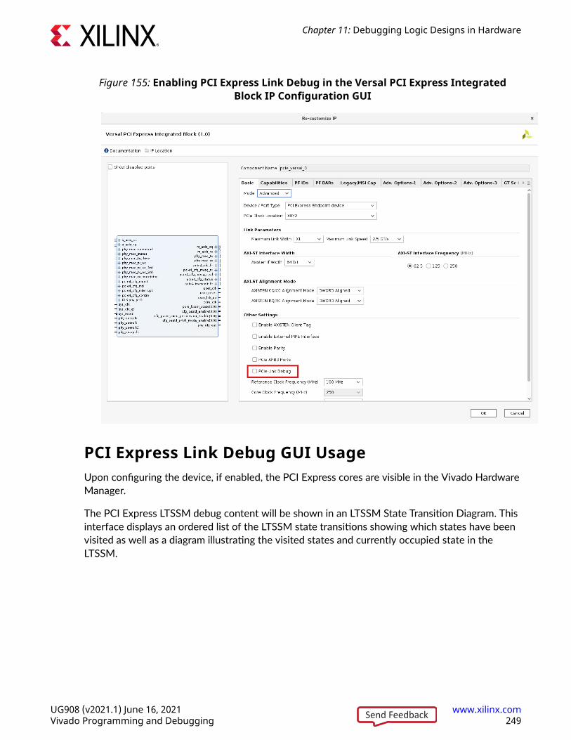
Figure 155: Enabling PCI Express Link Debug in the Versal PCI Express IntegratedBlock IP Configuration GUI
PCI Express Link Debug GUI UsageUpon configuring the device, if enabled, the PCI Express cores are visible in the Vivado HardwareManager.
The PCI Express LTSSM debug content will be shown in an LTSSM State Transition Diagram. Thisinterface displays an ordered list of the LTSSM state transitions showing which states have beenvisited as well as a diagram illustrating the visited states and currently occupied state in theLTSSM.
Chapter 11: Debugging Logic Designs in Hardware
UG908 (v2021.1) June 16, 2021 www.xilinx.comVivado Programming and Debugging 249Send Feedback
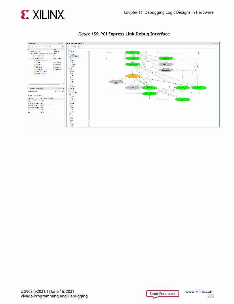
Figure 156: PCI Express Link Debug Interface
Chapter 11: Debugging Logic Designs in Hardware
UG908 (v2021.1) June 16, 2021 www.xilinx.comVivado Programming and Debugging 250Send Feedback
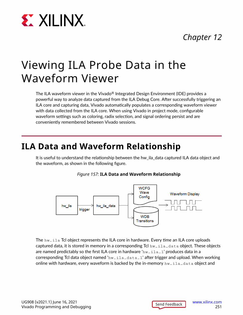
Chapter 12
Viewing ILA Probe Data in theWaveform Viewer
The ILA waveform viewer in the Vivado® Integrated Design Environment (IDE) provides apowerful way to analyze data captured from the ILA Debug Core. After successfully triggering anILA core and capturing data, Vivado automatically populates a corresponding waveform viewerwith data collected from the ILA core. When using Vivado in project mode, configurablewaveform settings such as coloring, radix selection, and signal ordering persist and areconveniently remembered between Vivado sessions.
ILA Data and Waveform RelationshipIt is useful to understand the relationship between the hw_ila_data captured ILA data object andthe waveform, as shown in the following figure.
Figure 157: ILA Data and Waveform Relationship
The hw_ila Tcl object represents the ILA core in hardware. Every time an ILA core uploadscaptured data, it is stored in memory in a corresponding Tcl hw_ila_data object. These objectsare named predictably so the first ILA core in hardware 'hw_ila_1' produces data in acorresponding Tcl data object named 'hw_ila_data_1' after trigger and upload. When workingonline with hardware, every waveform is backed by the in-memory hw_ila_data object and
Chapter 12: Viewing ILA Probe Data in the Waveform Viewer
UG908 (v2021.1) June 16, 2021 www.xilinx.comVivado Programming and Debugging 251Send Feedback
has a 1:1 correspondence with this object illustrated by the diagram in the previous figure. Foreach Tcl hw_ila_data object, a wave database (WDB) file and wave configuration (WCFG) fileare created and automatically tracked in a directory of the Vivado project. The previous figureillustrates the flow of data from the hardware hw_ila on the left through to the waveform displayon the right.
The combination of the wave configuration, WCFG, file and wave transition database, WDB, filecontain the waveform database and customizations displayed in the Vivado waveform userinterface. These waveform files are automatically managed in the Vivado ILA flow and users arenot expected to modify the WDB or WCFG files directly. The wave configuration can bemodified by changing objects in the waveform viewer (such as signal color, bus radix, signal order,markers, etc). This automatically saves the wave configuration changes to the appropriate WCFGfile in the Vivado project.
It is possible to archive waveform configurations and data for later viewing by using the Tclcommand write_hw_ila_data. This stores the hw_ila_data, wave database and waveconfiguration in an archive for later viewing offline. See the section, Saving and RestoringCaptured Data from the ILA Core for details on using read_hw_ila_data andwrite_hw_ila_data for offline storage and retrieval of waveforms.
Related Information
Saving and Restoring Captured Data from the ILA Core
Waveform Viewer LayoutThe ILA waveform viewer (sometimes referred to as waveform configuration) is composed ofseveral dynamic objects working together to provide a complete visualization tool for thecaptured ILA data, as shown in the following figure.
Chapter 12: Viewing ILA Probe Data in the Waveform Viewer
UG908 (v2021.1) June 16, 2021 www.xilinx.comVivado Programming and Debugging 252Send Feedback
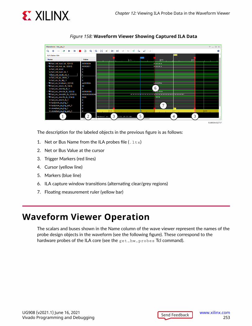
Figure 158: Waveform Viewer Showing Captured ILA Data
1 2 3 5 4
6
7
3
X18959-032717
The description for the labeled objects in the previous figure is as follows:
1. Net or Bus Name from the ILA probes file (.ltx)
2. Net or Bus Value at the cursor
3. Trigger Markers (red lines)
4. Cursor (yellow line)
5. Markers (blue line)
6. ILA capture window transitions (alternating clear/grey regions)
7. Floating measurement ruler (yellow bar)
Waveform Viewer OperationThe scalars and buses shown in the Name column of the wave viewer represent the names of theprobe design objects in the waveform (see the following figure). These correspond to thehardware probes of the ILA core (see the get_hw_probes Tcl command).
Chapter 12: Viewing ILA Probe Data in the Waveform Viewer
UG908 (v2021.1) June 16, 2021 www.xilinx.comVivado Programming and Debugging 253Send Feedback
Figure 159: ILA Probe Names and Values Shown in Waveform Viewer
Immediately after triggering and uploading ILA data for the first time, the waveform viewerpopulates with all probes connected to the ILA core. It is possible to customize probes in theviewer in addition to removing existing probes or adding new probes to the viewer. This sectioncovers the basic operation of the waveform viewer.
Removing Probes from the WaveformAll probes by default are added to the waveform during the first trigger and upload operation. Ifyou do not want the waveform to contain all probes, it is simple to remove probes from theviewer.
To remove a probe from the waveform viewer, right-click the scalar or bus to delete in the Namecolumn and select Delete from the pop up menu. Alternatively, select the signal or bus to deleteand press the Delete key. Probe transition data is not actually deleted from memory it is justhidden from view when probes are removed.
Chapter 12: Viewing ILA Probe Data in the Waveform Viewer
UG908 (v2021.1) June 16, 2021 www.xilinx.comVivado Programming and Debugging 254Send Feedback
Adding Probes to the WaveformTo add probes to the waveform, select the Probes to add for the associated ILA core in theDebug Probes window, right-click, and select Add Probes to Waveform from the pop-up menu.
To add another copy of a signal or bus to the Waveform window, select the signal or bus in theWaveform window. Then select Edit → Copy or type Ctrl+C. This copies the object to theclipboard. Select Edit → Paste or type Ctrl+V to paste a copy of the object in the waveform.
You can do the same using the Tcl command add_wave as shown below.
add_wave -into {hw_ila_data_1.wcfg} -radix hex { {counter1} }
In this example, probe counter1 is added to the Waveform Configuration window ofhw_ila_1 and its display radix in the Waveform window is set to hex.
Chapter 12: Viewing ILA Probe Data in the Waveform Viewer
UG908 (v2021.1) June 16, 2021 www.xilinx.comVivado Programming and Debugging 255Send Feedback
Using Waveform ILA Trigger and ExportFeatures
Figure 160: Waveform ILA Trigger and Export Features
Auto Re-Trigger
Run Trigger
Run Trigger Immediate
Stop Trigger
Export ILA Data
X16755-032717
• Enable Auto Re-Trigger: Select the Enable Auto Re-Trigger button on the Waveform windowtoolbar to enable Vivado IDE to automatically re-arm the ILA core associated with theWaveform window trigger after a successful trigger+upload+display operation has completed.
The captured data displayed in the Waveform window corresponding to the ILA core isoverwritten upon each successful trigger event. The Auto Re-Trigger option can be used withthe Run Trigger and Run Trigger Immediate operations. Click the Stop Trigger button to stopthe trigger currently in progress.
• Run Trigger: Arms the ILA core associated with the Waveform window to detect the triggerevent that is defined by the ILA core basic or advanced trigger settings.
• Run Trigger Immediate: Arms the ILA core associated with the Waveform window to triggerimmediately regardless of the ILA core trigger settings. This command is useful for detectingthe "aliveness" of the design by capturing any activity at the probe inputs of the ILA core.
• Stop Trigger: Stops the ILA core trigger of the ILA associated with the Waveform window.
Chapter 12: Viewing ILA Probe Data in the Waveform Viewer
UG908 (v2021.1) June 16, 2021 www.xilinx.comVivado Programming and Debugging 256Send Feedback
• Export ILA Data: Captures data from an ILA core and saves it to a file. The data can becaptured in either native, .csv, or .vcd format. On clicking this icon on the Waveformwindow toolbar the following dialog box appears.
Figure 161: Export ILA Data Dialog Box
The ILA core is the name of the ILA debug core to export data for. The format is a selectionamong Native, CSV, and VCD formats.
• Native format configures the write_hw_ila_data command to export the ILA data in theform of a default ILA file format file that can be used to import into Vivado and back again atanother point in time so that you can view previously captured ILA data.
• CSV format configures the write_hw_ila_data command to export the ILA data in theform of a .csv file that can be used to import the data into a spreadsheet or third-partyapplication.
• VCD file format configures the write_hw_ila_data command to export the ILA data in theform of a .vcd file that can be used to import into a third-party application or viewer.
IMPORTANT! While ILA data can be exported in the CSV, VCD, and native ILA format, only the native ILAformat can be imported into Vivado. Also, native ILA data imported into Vivado is supported only foroffline viewing of previously captured data. The probe signals cannot be used for other purposes such astriggering, etc.
Using the Zoom FeaturesToolbar buttons provide quick access to waveform zooming features (see the following figure).Alternatively, use the mouse wheel combined with the Ctrl key to zoom in and out of thecurrently selected waveform. It is important to note the zoom level is not persistent and will bereset between Vivado sessions.
Chapter 12: Viewing ILA Probe Data in the Waveform Viewer
UG908 (v2021.1) June 16, 2021 www.xilinx.comVivado Programming and Debugging 257Send Feedback
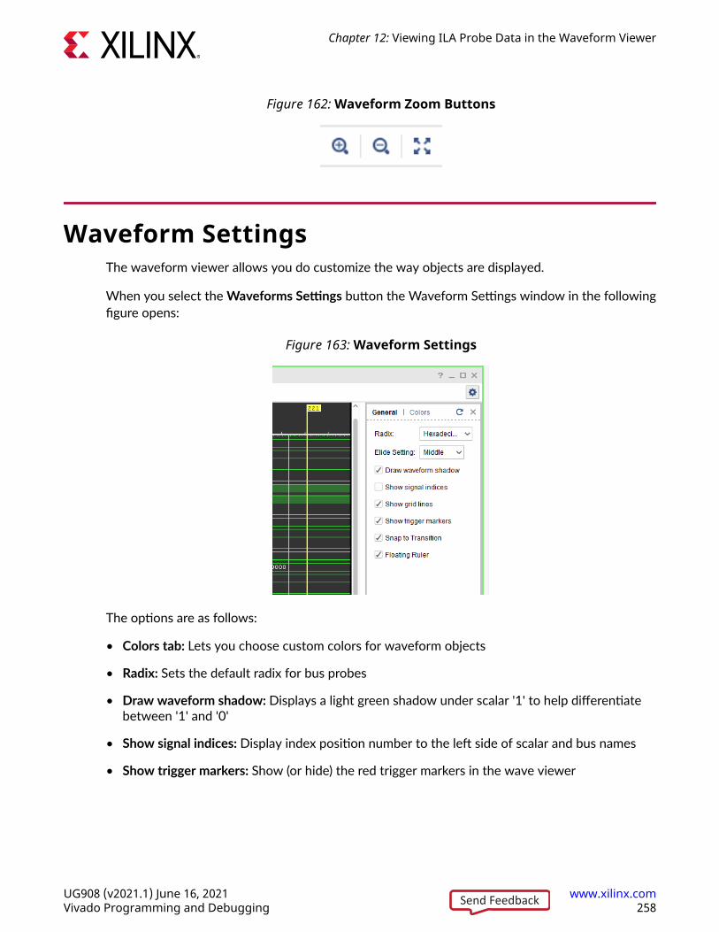
Figure 162: Waveform Zoom Buttons
Waveform SettingsThe waveform viewer allows you do customize the way objects are displayed.
When you select the Waveforms Settings button the Waveform Settings window in the followingfigure opens:
Figure 163: Waveform Settings
The options are as follows:
• Colors tab: Lets you choose custom colors for waveform objects
• Radix: Sets the default radix for bus probes
• Draw waveform shadow: Displays a light green shadow under scalar '1' to help differentiatebetween '1' and '0'
• Show signal indices: Display index position number to the left side of scalar and bus names
• Show trigger markers: Show (or hide) the red trigger markers in the wave viewer
Chapter 12: Viewing ILA Probe Data in the Waveform Viewer
UG908 (v2021.1) June 16, 2021 www.xilinx.comVivado Programming and Debugging 258Send Feedback
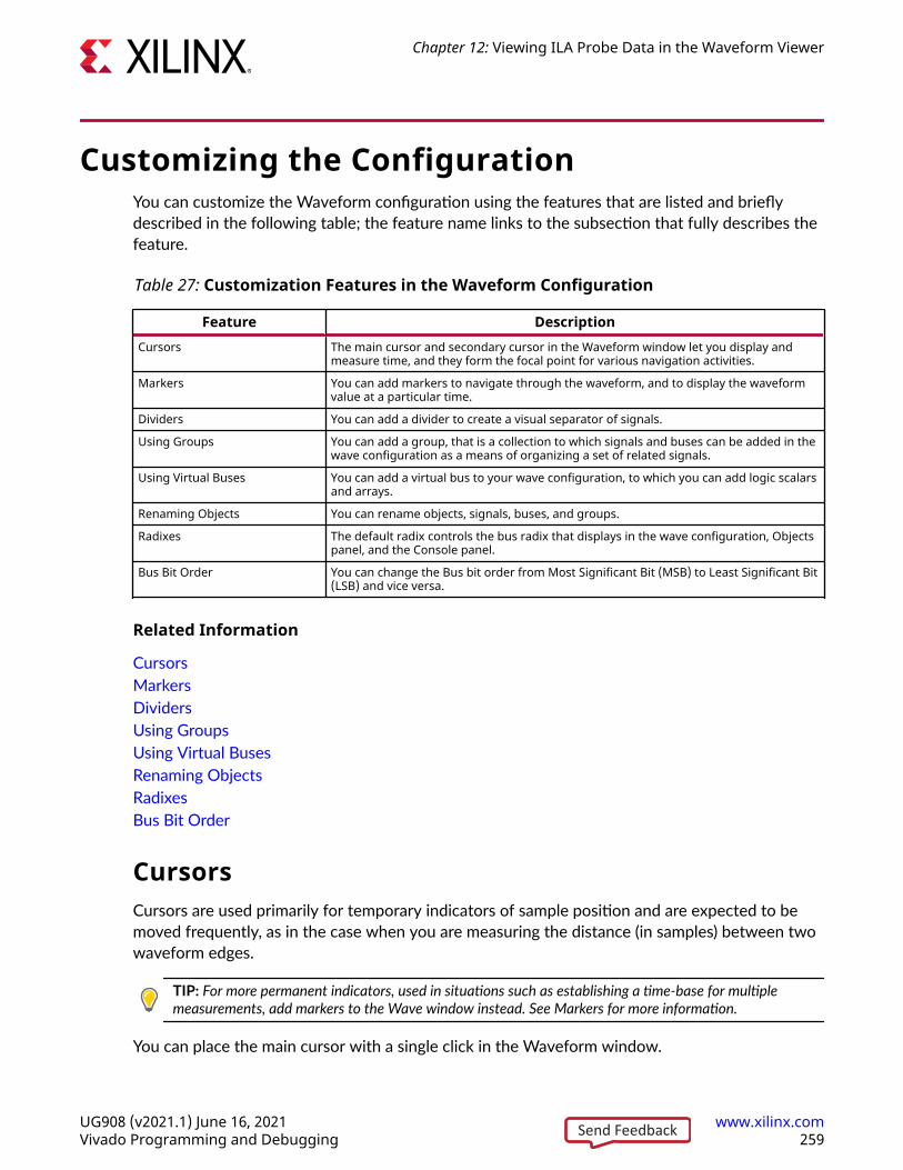
Customizing the ConfigurationYou can customize the Waveform configuration using the features that are listed and brieflydescribed in the following table; the feature name links to the subsection that fully describes thefeature.
Table 27: Customization Features in the Waveform Configuration
Feature DescriptionCursors The main cursor and secondary cursor in the Waveform window let you display and
measure time, and they form the focal point for various navigation activities.
Markers You can add markers to navigate through the waveform, and to display the waveformvalue at a particular time.
Dividers You can add a divider to create a visual separator of signals.
Using Groups You can add a group, that is a collection to which signals and buses can be added in thewave configuration as a means of organizing a set of related signals.
Using Virtual Buses You can add a virtual bus to your wave configuration, to which you can add logic scalarsand arrays.
Renaming Objects You can rename objects, signals, buses, and groups.
Radixes The default radix controls the bus radix that displays in the wave configuration, Objectspanel, and the Console panel.
Bus Bit Order You can change the Bus bit order from Most Significant Bit (MSB) to Least Significant Bit(LSB) and vice versa.
Related Information
CursorsMarkersDividersUsing GroupsUsing Virtual BusesRenaming ObjectsRadixesBus Bit Order
CursorsCursors are used primarily for temporary indicators of sample position and are expected to bemoved frequently, as in the case when you are measuring the distance (in samples) between twowaveform edges.
TIP: For more permanent indicators, used in situations such as establishing a time-base for multiplemeasurements, add markers to the Wave window instead. See Markers for more information.
You can place the main cursor with a single click in the Waveform window.
Chapter 12: Viewing ILA Probe Data in the Waveform Viewer
UG908 (v2021.1) June 16, 2021 www.xilinx.comVivado Programming and Debugging 259Send Feedback
To place a secondary cursor, Ctrl+Click and hold the waveform, and drag either left or right. Youcan see a flag that labels the location at the top of the cursor.
Alternatively, you can hold the Shift key and click a point in the waveform. The main cursorremains the original position, and the other cursor is at the point in the waveform that youclicked.
Note: To preserve the location of the secondary cursor while positioning the main cursor, hold the Shift keywhile clicking. When placing the secondary cursor by dragging, you must drag a minimum distance beforethe secondary cursor appears.
To move a cursor, hover over the cursor until you see the grab symbol, and click and drag thecursor to the new location.
As you drag the cursor in the Waveform window, you see a hollow or filled-in circle if the Snap toTransition button is selected, which is the default behavior.
• A hollow circle indicates that you are between transitions in the waveform of the selectedsignal.
• A filled-in circle indicates that you are hovering over the waveform transition of theselected signal. A secondary cursor can be hidden by clicking anywhere in the Waveformwindow where there is no cursor, marker, or floating ruler.
Related Information
Markers
MarkersUse a marker when you want to mark a significant event within your waveform in a permanentfashion. Markers allow you to measure distance (in samples) relevant to that marked event.
You can add, move, and delete markers as follows:
• You add markers to the wave configuration at the location of the main cursor.
1. Place the main cursor at the sample number where you want to add the marker by clickingin the Waveform window at the sample number or on the transition.
2. Select Edit → Markers → Add Marker, or click the Add Marker button.
A marker is placed at the cursor, or slightly offset if a marker already exists at the locationof the cursor. The sample number of the marker displays at the top of the line.
• You can move the marker to another location in the waveform using the drag and dropmethod. Click the marker label (at the top of the marker) and drag it to the location.
Chapter 12: Viewing ILA Probe Data in the Waveform Viewer
UG908 (v2021.1) June 16, 2021 www.xilinx.comVivado Programming and Debugging 260Send Feedback
○ The drag symbol indicates that the marker can be moved. As you drag the marker in theWaveform window, you see a hollow or filled-in circle if the Snap to Transition button isselected, which is the default behavior.
○ A filled-in circle indicates that you are hovering over a transition of the waveform for theselected signal or over another marker.
○ For markers, the filled-in circle is white.
○ A hollow circle indicates that are you between transitions in the waveform of theselected signal.
○ Release the mouse key to drop the marker to the new location.
• You can delete one or all markers with one command. Right-click over a marker, and do one ofthe following:
○ Select Delete Marker from the popup menu to delete a single marker.
○ Select Delete All Markers from the popup menu to delete all markers.
Note: You can also use the Delete key to delete a selected marker.
○ Use Edit → Undo to reverse a marker deletion.
Trigger MarkersThe red trigger marker (whose label is a red letter 'T') a special marker that indicates theoccurrence of the trigger event in the capture buffer. The position of the trigger marker in thebuffer directly corresponds to the Trigger Position setting (see Using the ILA Default Dashboard).
Note: The trigger markers are not movable using the same technique as regular markers. Set their positionusing the ILA core's Trigger Position property setting.
Related Information
Using the ILA Default Dashboard
DividersDividers create a visual separator between signals. You can add a divider to your waveconfiguration to create a visual separator of signals, as follows:
1. In a Name column of the Waveform window, click a signal to add a divider below that signal.
2. From the popup menu, select Edit → New Divider, or right-click and select New Divider.
The change is visual and nothing is added to the HDL code. The new divider is saved with thewave configuration file when you save the file.
You can move or delete Dividers as follows:
Chapter 12: Viewing ILA Probe Data in the Waveform Viewer
UG908 (v2021.1) June 16, 2021 www.xilinx.comVivado Programming and Debugging 261Send Feedback

• Move a Divider to another location in the waveform by dragging and dropping the dividername.
• To delete a Divider, highlight the divider, and click the Delete key, or right-click and selectDelete from the popup menu.
You can also rename Dividers; see Renaming Objects.
Related Information
Renaming Objects
Using GroupsA Group is a collection of expandable and collapsible categories, to which you can add signalsand buses in the wave configuration to organize related sets of signals. The group itself displaysno waveform data but can be expanded to show its contents or collapsed to hide them. You canadd, change, and remove groups.
To add a Group:
1. In a wave configuration, select one or more signals or buses to add to a group.
Note: A group can include dividers, virtual buses, and other groups.
2. Select Edit → New Group, or right-click and select New Group from the popup menu.
A Group that contains the selected signal or bus is added to the wave configuration.
A Group is represented with the Group button.
The change is visual and nothing is added to the ILA core.
You can move other signals or buses to the group by dragging and dropping the signal or busname.
You can move or remove Groups as follows:
• Move Groups to another location in the Name column by dragging and dropping the groupname.
• Remove a group, by highlighting it and selecting Edit → Wave Objects → Ungroup, or right-click and select Ungroup from the popup menu. Signals or buses formerly in the group areplaced at the top-level hierarchy in the wave configuration.
Groups can be renamed also; see Renaming Objects.
CAUTION! The Delete key removes the group and its nested signals and buses from the waveconfiguration.
Chapter 12: Viewing ILA Probe Data in the Waveform Viewer
UG908 (v2021.1) June 16, 2021 www.xilinx.comVivado Programming and Debugging 262Send Feedback
Related Information
Renaming Objects
Using Virtual BusesYou can add a virtual bus to your wave configuration, which is a grouping to which you can addlogic scalars and arrays. The virtual bus displays a bus waveform, which shows the signalwaveforms in the vertical order that they appear under the virtual bus, flattened to a one-dimensional array. You can then change or remove virtual buses after adding them.
To add a virtual bus:
1. In a wave configuration, select one or more signals or buses you want to add to a virtual bus.
2. Select Edit → New Virtual Bus, or right-click and select New Virtual Bus from the popupmenu.
The virtual bus is represented with the Virtual Bus button .
The change is visual and nothing is added to the HDL code.
You can move other signals or buses to the virtual bus by dragging and dropping the signal or busname. The new virtual bus and its nested signals or buses are saved when you save the waveconfiguration file. You can also move it to another location in the waveform by dragging anddropping the virtual bus name.
You can rename a virtual bus; see Renaming Objects.
To remove a virtual bus, and ungroup its contents, highlight the virtual bus, and select Edit → Wave Objects → Ungroup, or right-click and select Ungroup from the popup menu.
CAUTION! The Delete key removes the virtual bus and its nested signals and buses from the waveconfiguration.
Related Information
Renaming Objects
Renaming ObjectsYou can rename any object in the Waveform window, such as signals, dividers, groups, and virtualbuses.
1. Select the object name in the Name column.
2. Select Rename from the popup menu.
Chapter 12: Viewing ILA Probe Data in the Waveform Viewer
UG908 (v2021.1) June 16, 2021 www.xilinx.comVivado Programming and Debugging 263Send Feedback
3. Replace the name with a new one.
4. Press Enter or click outside the name to make the name change take effect.
You can also double-click the object name and then type a new name. The change is effectiveimmediately. Object name changes in the wave configuration do not affect the names of the netsattached to the ILA core probe inputs.
RadixesUnderstanding the type of data on your bus is important. You need to recognize the relationshipbetween the radix setting and the data type to use the waveform options of Digital and Analogeffectively. See Bus Radixes for more information about the radix setting and its effect on Analogwaveform analysis.
You can change the radix of an individual signal (ILA probe) in the Waveform window as follows:
1. Right-click a bus in the Waveform window.
2. Select Radix and the format you want from the drop-down menu:
• Binary
• Hexadecimal
• Unsigned Decimal
• Signed Decimal
• Octal
IMPORTANT! Changes to the radix of an item in the Objects window do not apply to values in theWaveform window or the Tcl Console. To change the radix of an individual signal (ILA probe) in theWaveform window, use the Waveform window popup menu.
• Maximum bus width of 64 bits on real. Incorrect values are possible for buses wider than64 bits.
• Floating point supports only 32- and 64-bit arrays.
Related Information
Bus Radixes
Using the Floating RulerThe floating ruler assists with sample measurements using a sample number base other than theabsolute sample numbers shown on the standard ruler at the top of the Waveform window.
Chapter 12: Viewing ILA Probe Data in the Waveform Viewer
UG908 (v2021.1) June 16, 2021 www.xilinx.comVivado Programming and Debugging 264Send Feedback

You can display (or hide) a floating ruler and move it to a location in the Waveform window. Thesample base (sample 0) of the floating ruler is the secondary cursor, or, if there is no secondarycursor, the selected marker.
The floating ruler button and the floating ruler itself are visible only when the secondary cursor(or selected marker) is present.
1. Do either of the following to display or hide a floating ruler:
• Place the secondary cursor.
• Select a marker.
2. Select View → Floating Ruler.
You only need to follow this procedure the first time. The floating ruler displays each time thesecondary cursor is placed or a marker is selected.
Select the command again to hide the floating ruler.
Bus Bit OrderYou can reverse the bus bit order in the wave configuration to switch between MSB-first andLSB-first signal representation.
To reverse the bit order:
1. Select a bus.
2. Right-click and select Reverse Bit Order.
The bus bit order is reversed. The Reverse Bit Order command is marked to show that this is thecurrent behavior.
Bus RadixesBus values are interpreted as numeric values, which are determined by the radix setting on thebus wave object, as follows:
• Binary, octal, hexadecimal, ASCII, and unsigned decimal radixes cause the bus values to beinterpreted as unsigned integers. The format of data on the bus must match the radix setting.
• Any non-0 or -1 bits cause the entire value to be interpreted as 0.
• The signed decimal radix causes the bus values to be interpreted as signed integers.
Chapter 12: Viewing ILA Probe Data in the Waveform Viewer
UG908 (v2021.1) June 16, 2021 www.xilinx.comVivado Programming and Debugging 265Send Feedback
Viewing Analog WaveformsTo convert a digital waveform to analog, do the following:
1. In the Name area of a Waveform window, right-click the bus.
2. Select Waveform Style and then Analog Settings to choose an appropriate drawing setting.
The digital drawing of the bus converts to an analog format.
You can adjust the height of either an analog waveform or a digital waveform by selecting andthen dragging the rows.
The following figure shows the Analog Settings dialog box with the settings for analog waveformdrawing.
Figure 164: Analog Settings Dialog Box
The Analog Settings dialog box options are as follows:
• Row Height: Specifies how tall to make the select wave objects, in pixels. Changing the rowheight does not change how much of a waveform is exposed or hidden vertically, but ratherstretches or contracts the height of the waveform.
When switching between Analog and Digital waveform styles, the row height is set to anappropriate default for the style (20 for digital, 100 for analog).
Chapter 12: Viewing ILA Probe Data in the Waveform Viewer
UG908 (v2021.1) June 16, 2021 www.xilinx.comVivado Programming and Debugging 266Send Feedback

• Y Range: Specifies the range of numeric values to be shown in the waveform area.
• Auto: Specifies that the range should continually expand whenever values in the visibletime range of the window are discovered to lie outside the current range.
• Fixed: Specifies that the time range is to remain at a constant interval.
• Min: Specifies the value displays at the bottom of the waveform area.
• Max: Specifies the value displays at the top.
Both values can be specified as floating point; however, if radix of the wave object radix isintegral, the values are truncated to integers.
• Interpolation Style: Specifies how the line connecting data points is to be drawn.
• Linear: Specifies a straight line between two data points.
• Hold: Specifies that of two data points, a horizontal line is drawn from the left point to theX-coordinate of the right point, then another line is drawn connecting that line to the rightdata point, in an L shape.
• Off Scale: Specifies how to draw waveform values that lie outside the Y range of thewaveform area.
• Hide: Specifies that outlying values are not shown, such that a waveform that reaches theupper or lower bound of the waveform area disappears until values are again within therange.
• Clip: Specifies that outlying values be altered so that they are at the top or bottom of thewaveform area, such that a waveform that reaches the upper- or lower-bound of thewaveform area follows the bound as a horizontal line until values are again within therange.
• Overlap: Specifies that the waveform be drawn wherever its values are, even if they lieoutside the bounds of the waveform area and overlap other waveforms, up to the limits ofthe wave window itself.
• Horizontal Line: Specifies whether to draw a horizontal rule at the given value. If the check-box is on, a horizontal grid line is drawn at the vertical position of the specified Y value, if thatvalue is within the Y range of the waveform.
As with Min and Max, the Y value accepts a floating point number but truncates it to aninteger if the radix of the selected wave objects is integral.
IMPORTANT! Analog settings are saved in a wave configuration; however, because control of zooming inthe Y dimension is highly interactive, unlike other wave object properties such as radix, they do not affectthe modification state of the wave configuration. Consequently, zoom settings are not saved with the waveconfiguration.
Chapter 12: Viewing ILA Probe Data in the Waveform Viewer
UG908 (v2021.1) June 16, 2021 www.xilinx.comVivado Programming and Debugging 267Send Feedback
Bus Plot ViewerIn addition to the analog waveform viewer the Vivado® Hardware Manager also supports the BusPlot Viewer, which allows viewing a bus's values over time, or one bus' values vs. another bus'values plotted on an X vs Y axis.
It can be helpful to view a Bus Plot when it is necessary to perform either of the following:
• Plotting analog sample data vs. time
• Plotting analog sample data vs. analog sample data
Figure 165: Bus Plot Showing Trigger Data vs. the Sample in Buffer
Creating a Bus PlotThe Bus Plot viewer can be used to plot previously captured ILA trace data. As such, it requiresthe path to an ILA bus plot data file (either .csv or .ila). By default, the Show Bus Plot dialogselects the last auto-saved ILA trigger data.
Example of Bus Plot Creation1. To create a Bus Plot, open the Vivado Hardware Manager and select Tools → Show Bus Plot.
Chapter 12: Viewing ILA Probe Data in the Waveform Viewer
UG908 (v2021.1) June 16, 2021 www.xilinx.comVivado Programming and Debugging 268Send Feedback
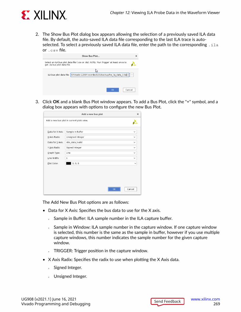
2. The Show Bus Plot dialog box appears allowing the selection of a previously saved ILA datafile. By default, the auto-saved ILA data file corresponding to the last ILA trace is auto-selected. To select a previously saved ILA data file, enter the path to the corresponding .ilaor .csv file.
3. Click OK and a blank Bus Plot window appears. To add a Bus Plot, click the "+" symbol, and adialog box appears with options to configure the new Bus Plot.
The Add New Bus Plot options are as follows:
• Data for X Axis: Specifies the bus data to use for the X axis.
○ Sample in Buffer: ILA sample number in the ILA capture buffer.
○ Sample in Window: ILA sample number in the capture window. If one capture windowis selected, this number is the same as the sample in buffer, however if you use multiplecapture windows, this number indicates the sample number for the given capturewindow.
○ TRIGGER: Trigger position in the capture window.
• X Axis Radix: Specifies the radix to use when plotting the X Axis data.
○ Signed Integer.
○ Unsigned Integer.
Chapter 12: Viewing ILA Probe Data in the Waveform Viewer
UG908 (v2021.1) June 16, 2021 www.xilinx.comVivado Programming and Debugging 269Send Feedback
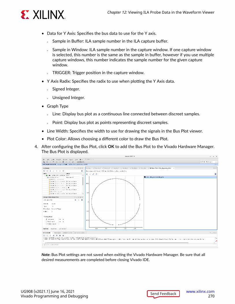
• Data for Y Axis: Specifies the bus data to use for the Y axis.
○ Sample in Buffer: ILA sample number in the ILA capture buffer.
○ Sample in Window: ILA sample number in the capture window. If one capture windowis selected, this number is the same as the sample in buffer, however if you use multiplecapture windows, this number indicates the sample number for the given capturewindow.
○ TRIGGER: Trigger position in the capture window.
• Y Axis Radix: Specifies the radix to use when plotting the Y Axis data.
○ Signed Integer.
○ Unsigned Integer.
• Graph Type
○ Line: Display bus plot as a continuous line connected between discreet samples.
○ Point: Display bus plot as points representing discreet samples.
• Line Width: Specifies the width to use for drawing the signals in the Bus Plot viewer.
• Plot Color: Allows choosing a different color to draw the Bus Plot.
4. After configuring the Bus Plot, click OK to add the Bus Plot to the Vivado Hardware Manager.The Bus Plot is displayed.
Note: Bus Plot settings are not saved when exiting the Vivado Hardware Manager. Be sure that alldesired measurements are completed before closing Vivado IDE.
Chapter 12: Viewing ILA Probe Data in the Waveform Viewer
UG908 (v2021.1) June 16, 2021 www.xilinx.comVivado Programming and Debugging 270Send Feedback
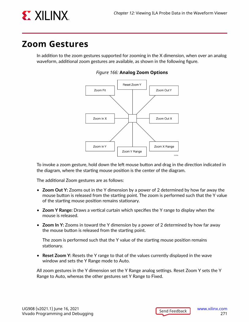
Zoom GesturesIn addition to the zoom gestures supported for zooming in the X dimension, when over an analogwaveform, additional zoom gestures are available, as shown in the following figure.
Figure 166: Analog Zoom Options
To invoke a zoom gesture, hold down the left mouse button and drag in the direction indicated inthe diagram, where the starting mouse position is the center of the diagram.
The additional Zoom gestures are as follows:
• Zoom Out Y: Zooms out in the Y dimension by a power of 2 determined by how far away themouse button is released from the starting point. The zoom is performed such that the Y valueof the starting mouse position remains stationary.
• Zoom Y Range: Draws a vertical curtain which specifies the Y range to display when themouse is released.
• Zoom In Y: Zooms in toward the Y dimension by a power of 2 determined by how far awaythe mouse button is released from the starting point.
The zoom is performed such that the Y value of the starting mouse position remainsstationary.
• Reset Zoom Y: Resets the Y range to that of the values currently displayed in the wavewindow and sets the Y Range mode to Auto.
All zoom gestures in the Y dimension set the Y Range analog settings. Reset Zoom Y sets the YRange to Auto, whereas the other gestures set Y Range to Fixed.
Chapter 12: Viewing ILA Probe Data in the Waveform Viewer
UG908 (v2021.1) June 16, 2021 www.xilinx.comVivado Programming and Debugging 271Send Feedback
Chapter 13
Debugging Designs PostImplementation
You might want to modify, add, or delete your debug cores post implementation. There are twoways to do it in Vivado® Design Suite.
If you want to replace the existing connections to the ILA cores, Xilinx recommends that you usethe ECO flow. The ECO flow operates on an implemented checkpoint (DCP) and could save youtime that could otherwise be spent in a complete re-route of the design.
If you want to add new ILA cores, delete existing ILA cores, or modify existing ILA cores (egresizing probe width, changing the data depth, etc.), Xilinx recommends that you use theIncremental Compile flow. The Incremental flow for debug cores operates on a synthesizeddesign or checkpoint (DCP) and uses a reference implemented checkpoint (ideally from aprevious run of implementation). This could save you time that could otherwise be spent in acomplete re-implementation of the design.
The sections below discuss each of these debug related flows in detail.
Using Vivado ECO Flow to Replace ExistingDebug Probes
It is possible to replace debug nets connected to an ILA core in a placed and routed designcheckpoint. You can do this by using the Engineering Change Order (ECO) flow. This is anadvanced design flow used for designs that are nearing completion, where you need to swapnets connected to an ILA probe port. This method serves two purposes:
• It saves you time. This feature lets you swap existing debug nets that are being probed fordifferent nets.
• It is minimally invasive. After replacing probed nets, it is necessary to route those nets to theinputs of the debug core. The rest of the design remains intact, thereby not only preservingprevious implementation results, but also reducing the possibility that a re-implementationwill hide the bug you are trying to find.
Chapter 13: Debugging Designs Post Implementation
UG908 (v2021.1) June 16, 2021 www.xilinx.comVivado Programming and Debugging 272Send Feedback
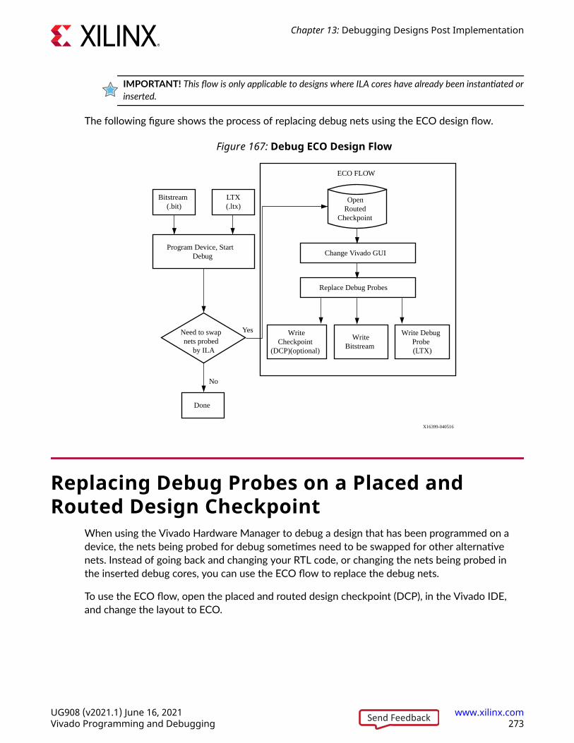
IMPORTANT! This flow is only applicable to designs where ILA cores have already been instantiated orinserted.
The following figure shows the process of replacing debug nets using the ECO design flow.
Figure 167: Debug ECO Design Flow
Need to swapnets probed
by ILA
Program Device, StartDebug
Bitstream(.bit)
LTX(.ltx)
Done
Open Routed
Checkpoint
Change Vivado GUI
Write Checkpoint
(DCP)(optional)
WriteBitstream
Write Debug Probe(LTX)
ECO FLOW
Yes
No
Replace Debug Probes
X16399-040516
Replacing Debug Probes on a Placed andRouted Design Checkpoint
When using the Vivado Hardware Manager to debug a design that has been programmed on adevice, the nets being probed for debug sometimes need to be swapped for other alternativenets. Instead of going back and changing your RTL code, or changing the nets being probed inthe inserted debug cores, you can use the ECO flow to replace the debug nets.
To use the ECO flow, open the placed and routed design checkpoint (DCP), in the Vivado IDE,and change the layout to ECO.
Chapter 13: Debugging Designs Post Implementation
UG908 (v2021.1) June 16, 2021 www.xilinx.comVivado Programming and Debugging 273Send Feedback
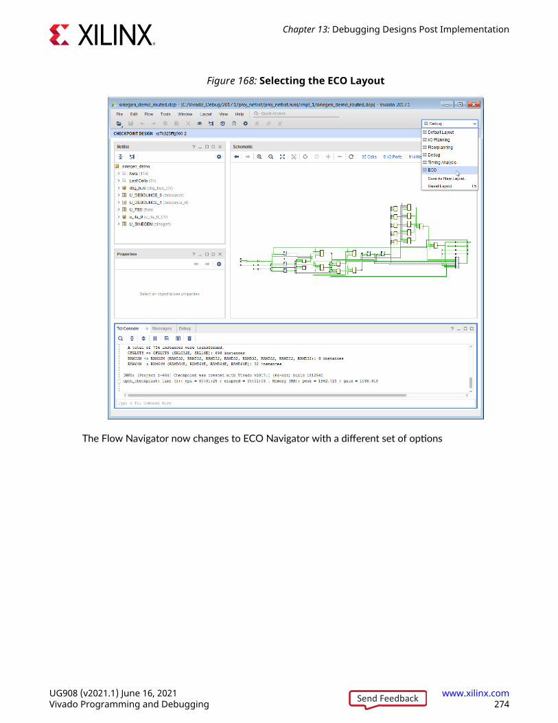
Figure 168: Selecting the ECO Layout
The Flow Navigator now changes to ECO Navigator with a different set of options
Chapter 13: Debugging Designs Post Implementation
UG908 (v2021.1) June 16, 2021 www.xilinx.comVivado Programming and Debugging 274Send Feedback
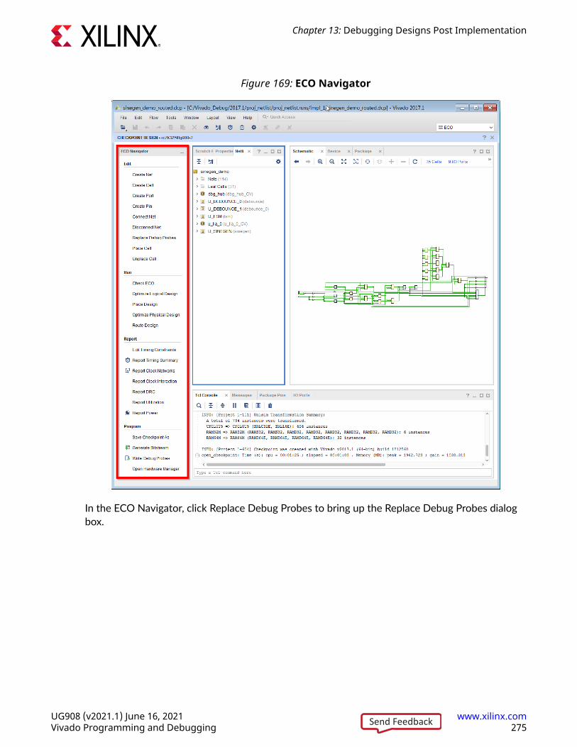
Figure 169: ECO Navigator
In the ECO Navigator, click Replace Debug Probes to bring up the Replace Debug Probes dialogbox.
Chapter 13: Debugging Designs Post Implementation
UG908 (v2021.1) June 16, 2021 www.xilinx.comVivado Programming and Debugging 275Send Feedback
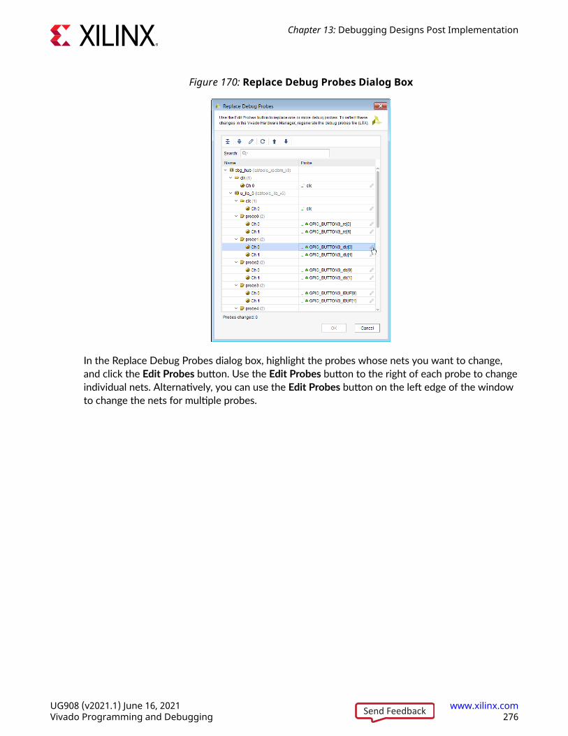
Figure 170: Replace Debug Probes Dialog Box
In the Replace Debug Probes dialog box, highlight the probes whose nets you want to change,and click the Edit Probes button. Use the Edit Probes button to the right of each probe to changeindividual nets. Alternatively, you can use the Edit Probes button on the left edge of the windowto change the nets for multiple probes.
Chapter 13: Debugging Designs Post Implementation
UG908 (v2021.1) June 16, 2021 www.xilinx.comVivado Programming and Debugging 276Send Feedback
Figure 171: Edit Probes Button
Click the Edit Probes button to bring up the Choose Nets dialog box, where you can choose netsto replace the existing ones.
Enter the Find criterion to select the nets you want to replace the existing nets. If the Findcriterion returns more than 10000 nets, refine you criterion and try again. Select the preferrednets on the Find Results on the left and click the arrow (->) to add those nets to the SelectedNames column on the right. Ensure the nets in the Selected Names column on the rightcorrespond to the number of nets being replaced. Click OK to continue.
Chapter 13: Debugging Designs Post Implementation
UG908 (v2021.1) June 16, 2021 www.xilinx.comVivado Programming and Debugging 277Send Feedback
Figure 172: Choose Nets Dialog Box
IMPORTANT! Once you have completed replacing all the debug probes necessary, rerouted them, andregenerated the bitstream, you must regenerate the debug probes file (.ltx).
TIP: You can also choose multiple nets or a bus by clicking on the Edit Probes button on the left in theReplace Debug Probes dialog box.
After you replace all the desired nets on the debug cores, click OK to bring up a confirmationdialog box to confirm the changes about to be made.
IMPORTANT! Check the Tcl Console to ensure that there are no Warnings/Errors.
Figure 173: Modify Debug Probe Tcl Messages
Chapter 13: Debugging Designs Post Implementation
UG908 (v2021.1) June 16, 2021 www.xilinx.comVivado Programming and Debugging 278Send Feedback
Deleting any net segment on the path of a net being probed could have an impact on the probenames displayed in the Hardware Manager. Vivado IDE picks the net segment closest to the netbeing probed with a MARK_DEBUG attribute on it. If there is no net segment with aMARK_DEBUG attribute, then the top level net is picked. If there is more than one net segmentwith a MARK_DEBUG attribute, the tool randomly selects one of those nets.
After you have replaced all the debug probe ports, you can save your modifications to a newcheckpoint using the Save Checkpoint As option in the ECO Navigator. The Replace DebugProbes command in the ECO Navigator needs to be run to generate a new .ltx file for thedebug probes. You should then generate a new bit file to program the device. You can thenconnect to the Vivado Hardware Manager to debug the design with the new changes.
Vivado ECO TCL Flow to Replace ExistingDebug Probes
You can use the Vivado Tcl flow as an alternative to the GUI flow described in the previoussections. Use the following Tcl command to modify nets being probed by the debug cores.
modify_debug_ports -probes [list {top/x_ila/probe0 0 top/inst_A/net_0} \ {top/x_ila/probe1 1 top/inst_A/net_a} {top/x_ila/probe1 2 top/inst_A/net_b}]
This command performs all of the netlist modifications to disconnect existing net connections tothe specified probe ports. In this example the existing net connections to probe port 0 at index 0,probe port 1 at index 1 and index 2 of the ILA are disconnected. Then each of these probes areconnected to the net specified net_0, net_a, and net_b respectively. The modifiedconnections are also routed automatically. Nets that become disconnected during the processare left unconnected.
Incremental Compile with Debug Core (ILA)Modifications
Incremental Compile is an advanced design flow for designs that are nearing completion, wheresmall changes are required. After resynthesizing these small changes, the flow:
• Speeds up place and route run time.
• Preserves QoR predictability by reusing prior placement and routing from a reference design.The flow is most effective when synthesis changes result in at least 95 percent similarity tothe reference design.
Chapter 13: Debugging Designs Post Implementation
UG908 (v2021.1) June 16, 2021 www.xilinx.comVivado Programming and Debugging 279Send Feedback

Incremental Debug changes are applied to a placed and routed design by re-implementing thedesign using the Incremental Compile design flow. This flow is recommended in situations where:
• The debug cores are absent from the existing implemented design or,
• You need to modify existing debug cores by changing probe widths, data depth, etc. or,
• You need to delete debug cores from the design.
Incremental Compile Flow DesignsThe Incremental Compile flow involves two different designs, the reference design and the currentdesign with debug core modifications.
Reference Design
The reference design is usually an earlier iteration or variation of the current design that hasbeen synthesized, placed, and routed. However, you can use a checkpoint that has any amount ofplacement, routing, or both. The reference design checkpoint (DCP) might be the product ofmany design iterations involving code changes, floorplanning, and revised constraints necessaryto close timing. After the current design is loaded, load the reference design checkpoint using theread_checkpoint -incremental <dcp> command. Loading the reference designcheckpoint with the -incremental option enables the Incremental Compile design flow forsubsequent place and route operations.
Current Design
The current design incorporates small debug related design changes or variations from thereference design. These changes or variations can include:
• Debug core RTL instantiation changes
• Debug core insertion changes
• Both debug core related RTL changes and insertion changes
To insert, delete, or modify debug cores to an existing design that has been implemented, openthe synthesized DCP or design, and use the debug insertion flow. Details on the debug insertionflow can be found in Using the Netlist Insertion Debug Probing Flow.
You can also modify existing debug cores or instantiate new debug cores into your existing RTLdesign. The Incremental Compile flow reuses placement and routing from the reference designalong with the new debug related modifications. Details on the debug instantiation flow can befound in HDL Instantiation Debug Probing Flow Overview.
Chapter 13: Debugging Designs Post Implementation
UG908 (v2021.1) June 16, 2021 www.xilinx.comVivado Programming and Debugging 280Send Feedback
Related Information
Using the Netlist Insertion Debug Probing FlowHDL Instantiation Debug Probing Flow Overview
Using Incremental CompileIn both Project Mode and Non-Project Mode, incremental place and route mode is entered whenyou load the reference design checkpoint using the read_checkpoint -incremental<reference_dcp_file> command where <reference_dcp_file> specifies the path andfile name of the reference design checkpoint. Loading the reference design checkpoint with the -incremental option enables the Incremental Compile design flow for subsequent place androute operations. In Non-Project Mode, read_checkpoint -incremental should: (1) followopt_design and; (2) precede place_design. If using the debug insertion flow the debug corerelated XDC commands should precede opt_design.
Using Incremental Compile in Non-Project Mode
To specify a design checkpoint file (DCP) to use as the reference design, and to run incrementalplace in Non-Project Mode:
1. Load the current design.
2. Run debug core commands.
3. Run opt_design.
IMPORTANT! Make sure the opt_design options and directives match those used in the originalreference run as closely as possible.
4. Run read_checkpoint -incremental <reference_dcp_file>.
5. Run place_design.
6. Run route_design.
# to load the current designlink_design;#Create the debug corecreate_debug_core u_ila_0 ila#set debug core propertiesset_property C_DATA_DEPTH 1024 [get_debug_cores u_ila_0]set_property C_TRIGIN_EN false [get_debug_cores u_ila_0]set_property C_TRIGOUT_EN false [get_debug_cores u_ila_0]set_property C_ADV_TRIGGER false [get_debug_cores u_ila_0]set_property C_INPUT_PIPE_STAGES 0 [get_debug_cores u_ila_0]set_property C_EN_STRG_QUAL false [get_debug_cores u_ila_0]set_property ALL_PROBE_SAME_MU true [get_debug_cores u_ila_0]set_property ALL_PROBE_SAME_MU_CNT 1 [get_debug_cores u_ila_0]#connect the probe ports in the debug core to the signals being probed in the designset_property port_width 1 [get_debug_ports u_ila_0/clk]connect_debug_port u_ila_0/clk [get_nets [list clk ]]
Chapter 13: Debugging Designs Post Implementation
UG908 (v2021.1) June 16, 2021 www.xilinx.comVivado Programming and Debugging 281Send Feedback

set_property port_width 1 [get_debug_ports u_ila_0/probe0]connect_debug_port u_ila_0/probe0 [get_nets [list A_or_B]]create_debug_port u_ila_0 probe opt_designread_checkpoint -incremental <reference_dcp_file>place_designroute_design
IMPORTANT! You must open the synthesized checkpoint to modify the debug cores in the design.Insertion of debug cores by opening a post-routed checkpoint is not supported.
Using Incremental Compile in Project Mode
In Project Mode, you can set the incremental compile option in the Design Runs window.
To set the incremental compile option:
1. Select a run in the Design Runs window.
2. Click Set Incremental Compile from the context menu.
3. In the Set Incremental Compile window, select a reference design checkpoint. This enablesincremental compile mode for the run.
4. Open the Synthesized netlist and optionally modify/add the debug cores instantiated in theRTL.
5. Use the Set Up Debug wizard to insert/delete/modify debug cores inserted into the design.
6. Implement Design.
IMPORTANT! You must open the synthesized design to modify the debug cores in the design.Insertion of debug cores by opening a post-routed design is not supported.
For more information on the Incremental Compile feature, see this link in the Vivado Design SuiteUser Guide: Implementation (UG904).
Examining the Similarity Between the ReferenceDesign and the Current DesignRun report_incremental_reuse to examine and report the similarity between a referencedesign checkpoint file and the current design. The report_incremental_reuse commandcompares the netlist from the reference design checkpoint with the current in-memory design,and reports the percentage of matching of cells, nets, and ports.
A higher degree of design similarity results in more effective reuse of placement and routing fromthe reference design. The greater the percentage of similarity between the reference design andcurrent design, the greater the opportunity for placement and routing reuse.
Chapter 13: Debugging Designs Post Implementation
UG908 (v2021.1) June 16, 2021 www.xilinx.comVivado Programming and Debugging 282Send Feedback
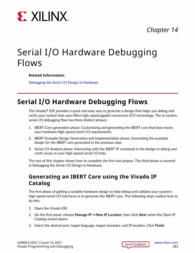
Chapter 14
Serial I/O Hardware DebuggingFlows
Related Information
Debugging the Serial I/O Design in Hardware
Serial I/O Hardware Debugging FlowsThe Vivado® IDE provides a quick and easy way to generate a design that helps you debug andverify your system that uses Xilinx high-speed gigabit transceiver (GT) technology. The in-systemserial I/O debugging flow has three distinct phases:
1. IBERT Core generation phase: Customizing and generating the IBERT core that best meetsyour hardware high-speed serial I/O requirements.
2. IBERT Example Design Generation and Implementation phase: Generating the exampledesign for the IBERT core generated in the previous step.
3. Serial I/O Analysis phase: Interacting with the IBERT IP contained in the design to debug andverify issues in your high-speed serial I/O links.
The rest of this chapter shows how to complete the first two phases. The third phase is coveredin Debugging the Serial I/O Design in Hardware.
Generating an IBERT Core using the Vivado IPCatalogThe first phase of getting a suitable hardware design to help debug and validate your system'shigh-speed serial I/O interfaces is to generate the IBERT core. The following steps outline how todo this:
1. Open the Vivado IDE.
2. On the first panel, choose Manage IP → New IP Location, then click Next when the Open IPCatalog wizard opens.
3. Select the desired part, target language, target simulator, and IP location. Click Finish.
Chapter 14: Serial I/O Hardware Debugging Flows
UG908 (v2021.1) June 16, 2021 www.xilinx.comVivado Programming and Debugging 283Send Feedback
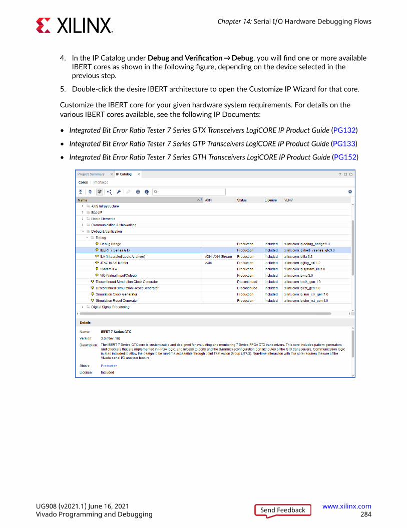
4. In the IP Catalog under Debug and Verification → Debug, you will find one or more availableIBERT cores as shown in the following figure, depending on the device selected in theprevious step.
5. Double-click the desire IBERT architecture to open the Customize IP Wizard for that core.
Customize the IBERT core for your given hardware system requirements. For details on thevarious IBERT cores available, see the following IP Documents:
• Integrated Bit Error Ratio Tester 7 Series GTX Transceivers LogiCORE IP Product Guide (PG132)
• Integrated Bit Error Ratio Tester 7 Series GTP Transceivers LogiCORE IP Product Guide (PG133)
• Integrated Bit Error Ratio Tester 7 Series GTH Transceivers LogiCORE IP Product Guide (PG152)
Chapter 14: Serial I/O Hardware Debugging Flows
UG908 (v2021.1) June 16, 2021 www.xilinx.comVivado Programming and Debugging 284Send Feedback

Generating and Implementing the IBERT ExampleDesignAfter generating the IBERT IP core, it appears in the Sources window as ibert_7series_gtxor something similar. To generate the example design, right-click the IBERT IP in the Sourceswindow and select Open IP Example Design, then specify the desired location of the exampledesign project in the resulting dialog window. This command opens a new Vivado projectwindow for the example design and adds the proper top-level wrapper and constraints file to theproject, as shown in the following figure.
IMPORTANT! Modification of the IBERT IP example design is not reccomended and may result infunctional issues when interacting with the IBERT IP core in hardware.
Once the example design is generated, you can implement the IBERT example design throughbitstream creation core by clicking Generate Bitstream in the Program and Debug section of theVivado IDE flow navigator or by running the following Tcl commands:
launch_runs impl_1 -to_step write_bitstreamwait_on_run impl_1
Refer to the Vivado Design Suite User Guide: Design Flows Overview (UG892) for more details onthe various ways you can implement your design.
Chapter 14: Serial I/O Hardware Debugging Flows
UG908 (v2021.1) June 16, 2021 www.xilinx.comVivado Programming and Debugging 285Send Feedback
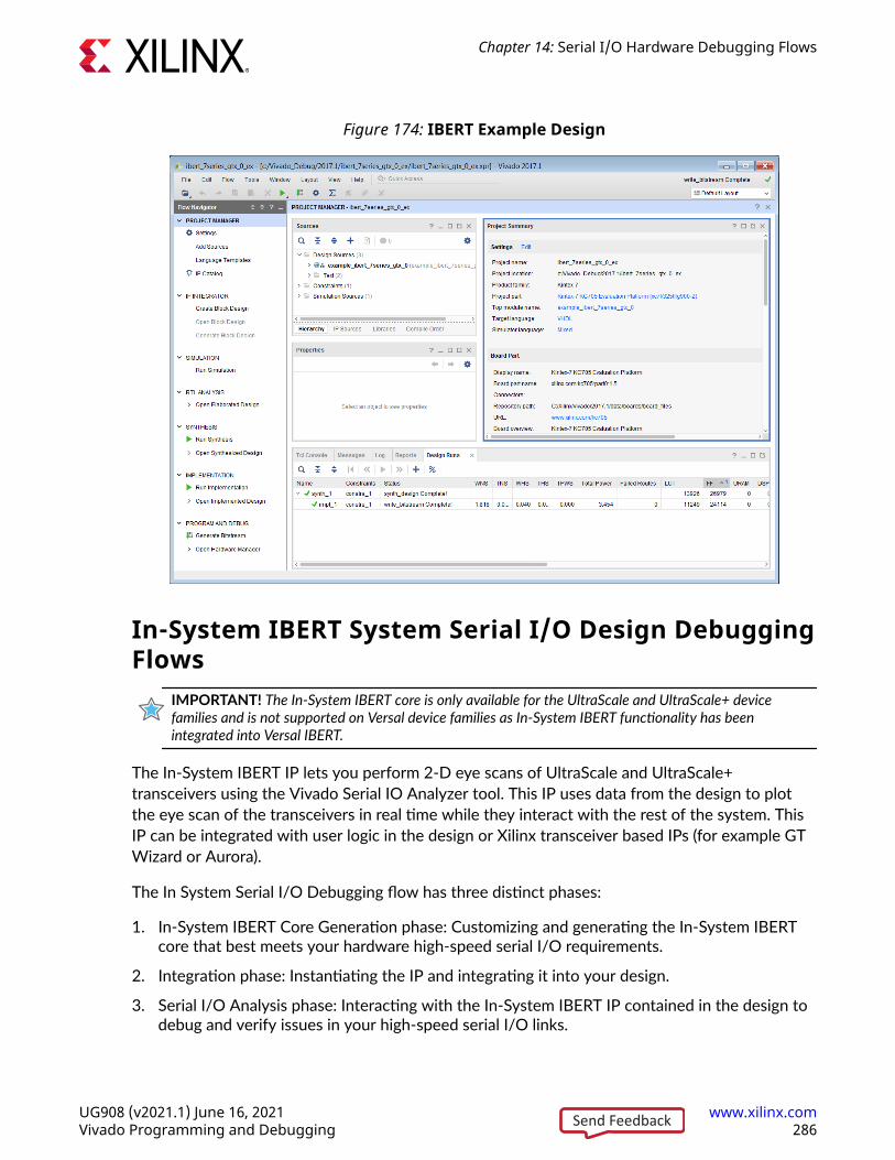
Figure 174: IBERT Example Design
In-System IBERT System Serial I/O Design DebuggingFlows
IMPORTANT! The In-System IBERT core is only available for the UltraScale and UltraScale+ devicefamilies and is not supported on Versal device families as In-System IBERT functionality has beenintegrated into Versal IBERT.
The In-System IBERT IP lets you perform 2-D eye scans of UltraScale and UltraScale+transceivers using the Vivado Serial IO Analyzer tool. This IP uses data from the design to plotthe eye scan of the transceivers in real time while they interact with the rest of the system. ThisIP can be integrated with user logic in the design or Xilinx transceiver based IPs (for example GTWizard or Aurora).
The In System Serial I/O Debugging flow has three distinct phases:
1. In-System IBERT Core Generation phase: Customizing and generating the In-System IBERTcore that best meets your hardware high-speed serial I/O requirements.
2. Integration phase: Instantiating the IP and integrating it into your design.
3. Serial I/O Analysis phase: Interacting with the In-System IBERT IP contained in the design todebug and verify issues in your high-speed serial I/O links.
Chapter 14: Serial I/O Hardware Debugging Flows
UG908 (v2021.1) June 16, 2021 www.xilinx.comVivado Programming and Debugging 286Send Feedback

Details about the In-System IBERT Core Generation phase and the Integration phase are coveredthe remainder of this section. For details of the Serial I/O Analysis phase, see Debugging theSerial I/O Design in Hardware.
Related Information
Debugging the Serial I/O Design in Hardware
Generating an In-System IBERT Core Using the Vivado IP Catalog
The first phase of debugging your design's high-speed serial I/O interfaces is to generate the In-System IBERT core.
To do this, follow these steps:
1. Open the Vivado IDE
2. On the first panel, choose Manage IP → New IP Location, then click Next when the Open IPCatalog wizard opens.
3. Select the desired part, target language, target simulator, and IP location. Click Finish.
4. In the IP Catalog under Debug and Verification → Debug , you will find one or more availableIn-System IBERT cores depending on the device selected in the previous step.
5. Double-click the desired In-System IBERT architecture to open the Customize IP Wizard forthat core
Customize the In-System IBERT core for your given hardware system requirements. For detailson the In-System IBERT cores, see the In-System IBERT LogiCORE IP Product Guide (PG246).
Instantiating the IP and integrating In-System IBERT IP in the UserDesign
After generating the In-System IBERT IP core do the following:
1. Open your top level RTL file to edit and add the In-System IBERT core generated in the abovestep.
2. Copy the instantiation template of the In-System IBERT core generated by the tool andinstantiate it in the RTL file.
3. Connect the ports of your transceiver to the In-System IBERT IP.
For a detailed example of how to integrate In-System IBERT into the user design, see Chapter 5"Example Designs" of the following IP Document: In-System IBERT LogiCORE IP Product Guide(PG246).
Chapter 14: Serial I/O Hardware Debugging Flows
UG908 (v2021.1) June 16, 2021 www.xilinx.comVivado Programming and Debugging 287Send Feedback
TIP: Ensure that you have read the FAQ section of the In-System IBERT LogiCORE IP Product Guide(PG246), which lists some recommendations for issues you could encounter while integrating this IP intoyour design.
4. Synthesize and implement the design.
Chapter 14: Serial I/O Hardware Debugging Flows
UG908 (v2021.1) June 16, 2021 www.xilinx.comVivado Programming and Debugging 288Send Feedback
Chapter 15
Versal Serial I/O HardwareDebugging Flows
Versal™ ACAPs no longer require the generation of IBERT IP as the necessary logic required touse in-system. Serial I/O debug is now integrated into the GTY transceiver architecture. Anydesign that uses the GTY transceivers can be used for Serial I/O hardware debugging. The VersalSerial I/O hardware debugging flow has two distinct phases:
1. Design creation. Customizing and generating a design that uses the device's GTYtransceivers, typically using the Versal ACAP transceivers wizard.
2. Serial I/O analysis. Interacting with the GTY transceivers in the design using the Vivado®
Hardware Manager to debug and verify issues in your high-speed serial I/O links.
Note: Versal IBERT can use internal pattern generators such as PRBS and user data from the design. Forthis reason the In-System IBERT core is not supported for Versal devices. To gain functionality similar to In-System IBERT change the pattern to user data.
For more information, see the Versal ACAP Transceivers Wizard LogiCORE IP Product Guide(PG331).
Chapter 15: Versal Serial I/O Hardware Debugging Flows
UG908 (v2021.1) June 16, 2021 www.xilinx.comVivado Programming and Debugging 289Send Feedback

Chapter 16
Debugging the Serial I/O Design inHardware
Once you have IBERT core implemented, you can use the run time serial I/O analyzer features todebug the design in hardware. Only IBERT cores version v3.0 and later can be accessed using theserial I/O analyzer feature.
Using Vivado Serial I/O Analyzer to Debug theDesign
The Vivado® serial I/O analyzer feature is used to interact with IBERT debug IP cores that are inyour design. To access the Vivado serial I/O analyzer feature, click the Open Hardware Managerbutton in the Program and Debug section of the Flow Navigator.
The steps to debug your design in hardware are:
1. Connect to the hardware target and programming the FPGA with the bit file.
2. Create Links.
3. Modify link settings and examine status.
4. Run scans as needed.
Connecting to the Hardware Target andProgramming the DeviceProgramming an FPGA or ACAP prior to debugging involves exactly the same steps described inProgramming the FPGA or ACAP. After programming the device with the .pdi file that containsthe IBERT core, the Hardware window now shows the components of the IBERT core with theRTL instance name shown in parenthesis, that were detected when scanning the device (see thefollowing figure).
IMPORTANT! In designs using the In-System IBERT IP for UltraScale and UltraScale+ designs, you will seethe In-System IBERT core being detected in the Hardware window.
Chapter 16: Debugging the Serial I/O Design in Hardware
UG908 (v2021.1) June 16, 2021 www.xilinx.comVivado Programming and Debugging 290Send Feedback
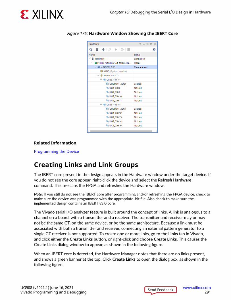
Figure 175: Hardware Window Showing the IBERT Core
Related Information
Programming the Device
Creating Links and Link GroupsThe IBERT core present in the design appears in the Hardware window under the target device. Ifyou do not see the core appear, right-click the device and select the Refresh Hardwarecommand. This re-scans the FPGA and refreshes the Hardware window.
Note: If you still do not see the IBERT core after programming and/or refreshing the FPGA device, check tomake sure the device was programmed with the appropriate .bit file. Also check to make sure theimplemented design contains an IBERT v3.0 core.
The Vivado serial I/O analyzer feature is built around the concept of links. A link is analogous to achannel on a board, with a transmitter and a receiver. The transmitter and receiver may or maynot be the same GT, on the same device, or be the same architecture. Because a link must beassociated with both a transmitter and receiver, connecting an external pattern generator to asingle GT receiver is not supported. To create one or more links, go to the Links tab in Vivado,and click either the Create Links button, or right-click and choose Create Links. This causes theCreate Links dialog window to appear, as shown in the following figure.
When an IBERT core is detected, the Hardware Manager notes that there are no links present,and shows a green banner at the top. Click Create Links to open the dialog box, as shown in thefollowing figure.
Chapter 16: Debugging the Serial I/O Design in Hardware
UG908 (v2021.1) June 16, 2021 www.xilinx.comVivado Programming and Debugging 291Send Feedback
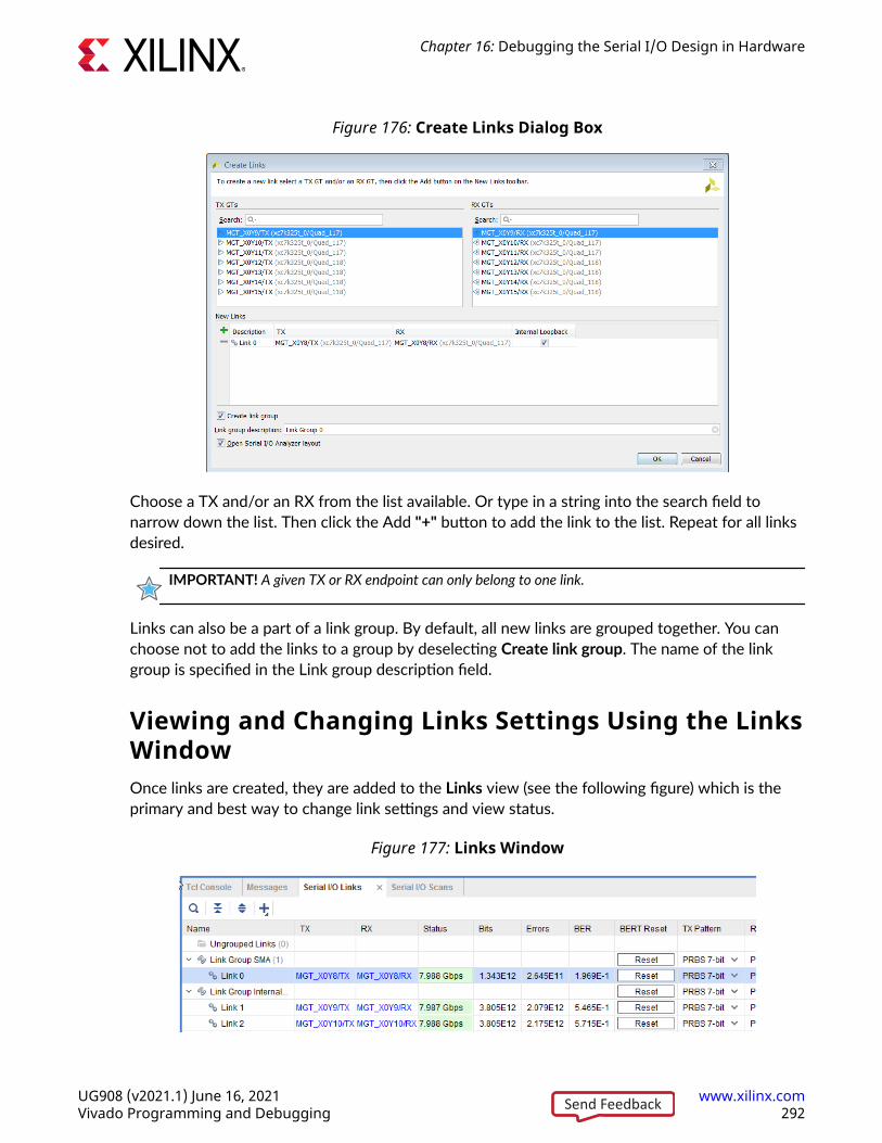
Figure 176: Create Links Dialog Box
Choose a TX and/or an RX from the list available. Or type in a string into the search field tonarrow down the list. Then click the Add "+" button to add the link to the list. Repeat for all linksdesired.
IMPORTANT! A given TX or RX endpoint can only belong to one link.
Links can also be a part of a link group. By default, all new links are grouped together. You canchoose not to add the links to a group by deselecting Create link group. The name of the linkgroup is specified in the Link group description field.
Viewing and Changing Links Settings Using the LinksWindowOnce links are created, they are added to the Links view (see the following figure) which is theprimary and best way to change link settings and view status.
Figure 177: Links Window
Chapter 16: Debugging the Serial I/O Design in Hardware
UG908 (v2021.1) June 16, 2021 www.xilinx.comVivado Programming and Debugging 292Send Feedback
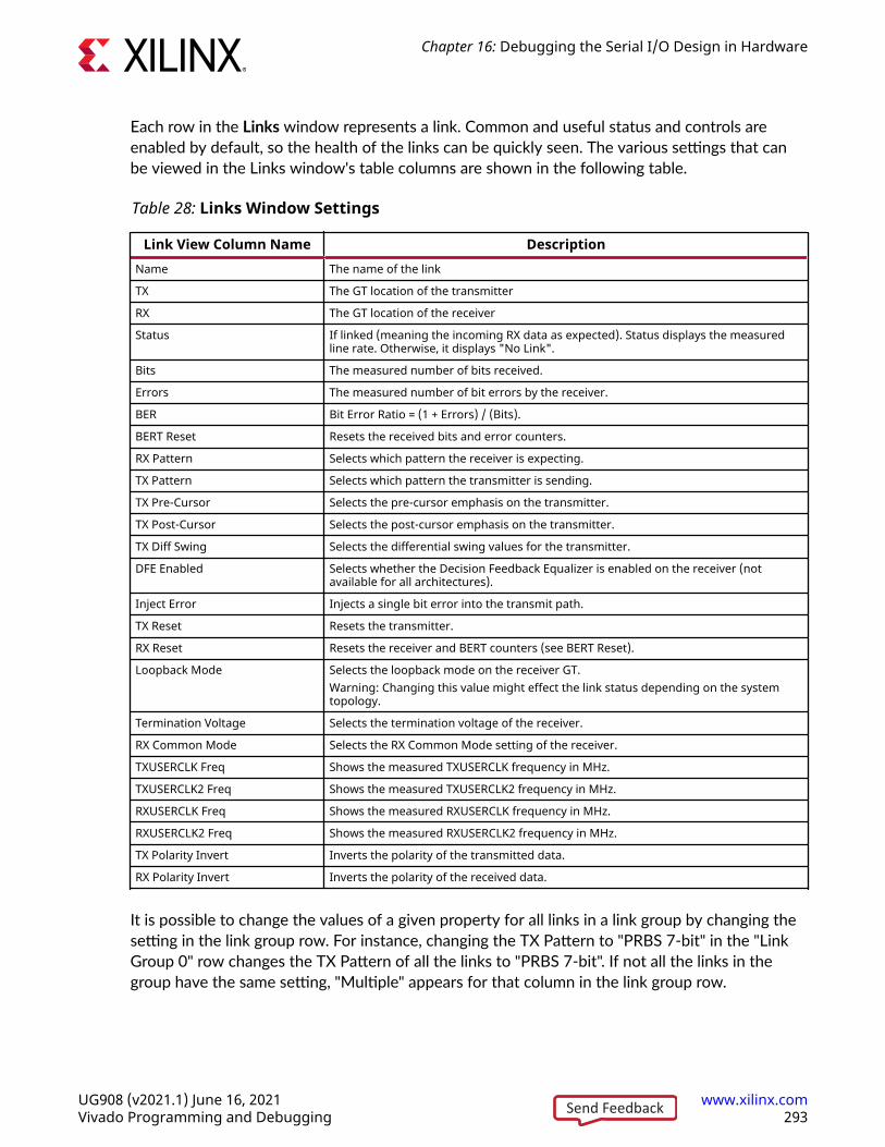
Each row in the Links window represents a link. Common and useful status and controls areenabled by default, so the health of the links can be quickly seen. The various settings that canbe viewed in the Links window's table columns are shown in the following table.
Table 28: Links Window Settings
Link View Column Name DescriptionName The name of the link
TX The GT location of the transmitter
RX The GT location of the receiver
Status If linked (meaning the incoming RX data as expected). Status displays the measuredline rate. Otherwise, it displays "No Link".
Bits The measured number of bits received.
Errors The measured number of bit errors by the receiver.
BER Bit Error Ratio = (1 + Errors) / (Bits).
BERT Reset Resets the received bits and error counters.
RX Pattern Selects which pattern the receiver is expecting.
TX Pattern Selects which pattern the transmitter is sending.
TX Pre-Cursor Selects the pre-cursor emphasis on the transmitter.
TX Post-Cursor Selects the post-cursor emphasis on the transmitter.
TX Diff Swing Selects the differential swing values for the transmitter.
DFE Enabled Selects whether the Decision Feedback Equalizer is enabled on the receiver (notavailable for all architectures).
Inject Error Injects a single bit error into the transmit path.
TX Reset Resets the transmitter.
RX Reset Resets the receiver and BERT counters (see BERT Reset).
Loopback Mode Selects the loopback mode on the receiver GT.Warning: Changing this value might effect the link status depending on the systemtopology.
Termination Voltage Selects the termination voltage of the receiver.
RX Common Mode Selects the RX Common Mode setting of the receiver.
TXUSERCLK Freq Shows the measured TXUSERCLK frequency in MHz.
TXUSERCLK2 Freq Shows the measured TXUSERCLK2 frequency in MHz.
RXUSERCLK Freq Shows the measured RXUSERCLK frequency in MHz.
RXUSERCLK2 Freq Shows the measured RXUSERCLK2 frequency in MHz.
TX Polarity Invert Inverts the polarity of the transmitted data.
RX Polarity Invert Inverts the polarity of the received data.
It is possible to change the values of a given property for all links in a link group by changing thesetting in the link group row. For instance, changing the TX Pattern to "PRBS 7-bit" in the "LinkGroup 0" row changes the TX Pattern of all the links to "PRBS 7-bit". If not all the links in thegroup have the same setting, "Multiple" appears for that column in the link group row.
Chapter 16: Debugging the Serial I/O Design in Hardware
UG908 (v2021.1) June 16, 2021 www.xilinx.comVivado Programming and Debugging 293Send Feedback
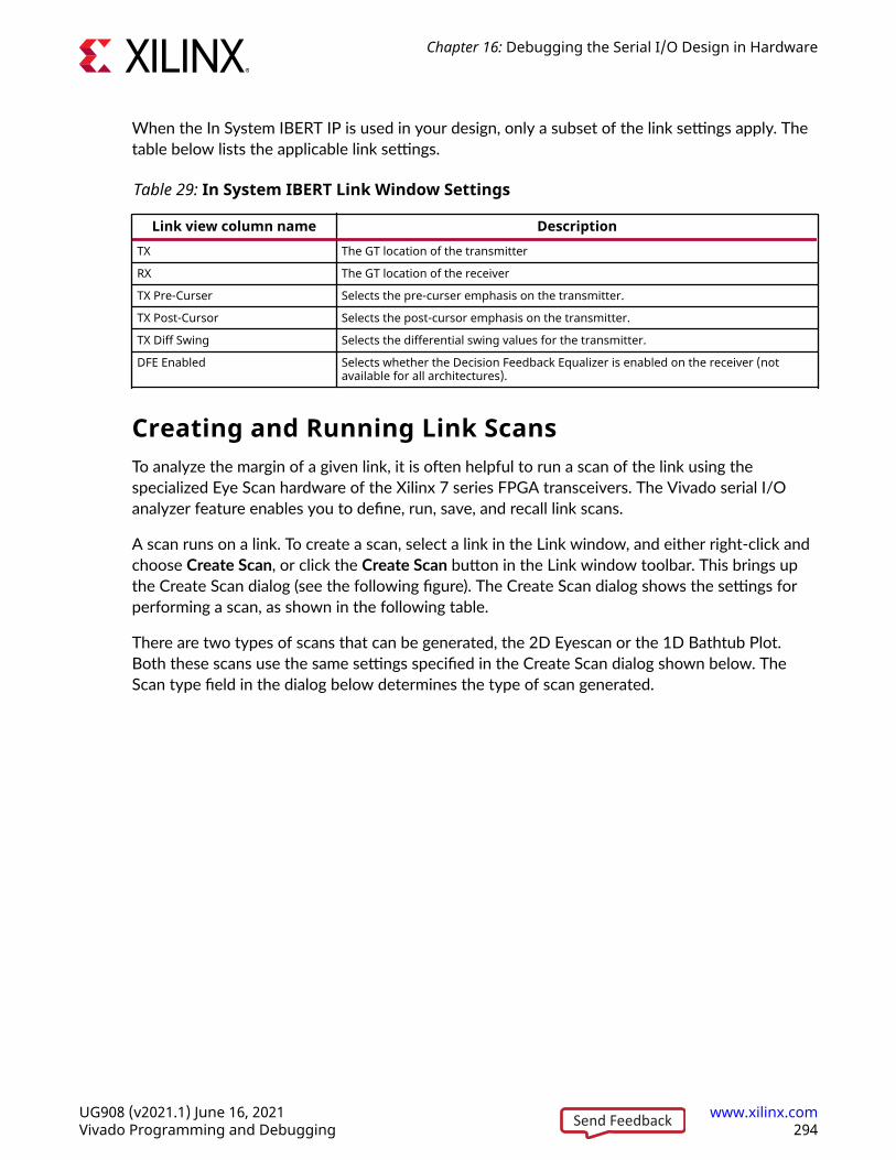
When the In System IBERT IP is used in your design, only a subset of the link settings apply. Thetable below lists the applicable link settings.
Table 29: In System IBERT Link Window Settings
Link view column name DescriptionTX The GT location of the transmitter
RX The GT location of the receiver
TX Pre-Curser Selects the pre-curser emphasis on the transmitter.
TX Post-Cursor Selects the post-cursor emphasis on the transmitter.
TX Diff Swing Selects the differential swing values for the transmitter.
DFE Enabled Selects whether the Decision Feedback Equalizer is enabled on the receiver (notavailable for all architectures).
Creating and Running Link ScansTo analyze the margin of a given link, it is often helpful to run a scan of the link using thespecialized Eye Scan hardware of the Xilinx 7 series FPGA transceivers. The Vivado serial I/Oanalyzer feature enables you to define, run, save, and recall link scans.
A scan runs on a link. To create a scan, select a link in the Link window, and either right-click andchoose Create Scan, or click the Create Scan button in the Link window toolbar. This brings upthe Create Scan dialog (see the following figure). The Create Scan dialog shows the settings forperforming a scan, as shown in the following table.
There are two types of scans that can be generated, the 2D Eyescan or the 1D Bathtub Plot.Both these scans use the same settings specified in the Create Scan dialog shown below. TheScan type field in the dialog below determines the type of scan generated.
Chapter 16: Debugging the Serial I/O Design in Hardware
UG908 (v2021.1) June 16, 2021 www.xilinx.comVivado Programming and Debugging 294Send Feedback
Figure 178: Create Scan Dialog
Table 30: Scan Settings
Scan Setting DescriptionDescription A user-defined name for the scan.
Scan Type The type of scan to run. This can be a 2D Eyescan or a 1D Bathtub plot.
Horizontal Increment Allows you to choose to scan the eye at a reduced resolution, but at increased speed byskipping horizontal codes.
Horizontal Range Reducing the horizontal range increases the scan speed. By default, the entire eye is scanned(-1/2 of a unit interval to +1/2 in reference to the center of the eye).
Vertical Increment Allows you to choose to scan the eye at a reduced resolution, but increased speed by skippingvertical codes.
Vertical Range Reducing the vertical range increases the scan speed. By default, the entire eye is scanned.
Dwell BER Each point in the chart is scanned for a certain amount of time. Dwell BER allows you tochoose the scan depth by selecting the desired Bit Error Ratio.
Dwell Time Dwell Time allows you to choose the scan depth by inputting the desired time in seconds.The Dwell time setting is not supported on designs that use In System IBERT IP.
By default, the scan is run after it is created. If you do not want to run the scan, and only defineit, uncheck the Run Scan check box.
If a scan is created, but not run, it can be subsequently run or run by right-clicking on a scan inthe Scans window and choosing Run Scan (see the following figure). While a scan is running, itcan be prematurely stopped by right-clicking on a scan and choosing Stop Scan, or clicking theStop Scan button in the Scans window toolbar.
Chapter 16: Debugging the Serial I/O Design in Hardware
UG908 (v2021.1) June 16, 2021 www.xilinx.comVivado Programming and Debugging 295Send Feedback
Figure 179: Scans Window
Creating and Running Link SweepsTo analyze the margin of a given link, it can be helpful to run multiple scans of the link withdifferent MGT settings. This helps determine which settings are the best. The Vivado serial I/Oanalyzer feature enables you to define, run, save, and recall link sweeps, which are a collection oflink scans.
A sweep runs on a link. To create a sweep, select a link in the Link window, and either right-clickand choose Create Sweep, or click the Create Sweep button in the Link window toolbar. This willbring up the Create Sweep dialog box, which looks similar to the Create Scan dialog box, exceptthat it has additional options for defining which properties to sweep, and how.
Figure 180: Create Sweep Dialog Box
Chapter 16: Debugging the Serial I/O Design in Hardware
UG908 (v2021.1) June 16, 2021 www.xilinx.comVivado Programming and Debugging 296Send Feedback
Table 31: Sweep Settings
Sweep Setting DescriptionDescription A user-defined name for the sweep.
Scan Type The type of scan to run. This can be a 2D Eyescan or a 1D Bathtub plot.
Horizontal Increment Allows you to scan the eye at a reduced resolution, but at increased speed byskipping horizontal codes.
Horizontal Range Reducing the horizontal range increases the scan speed. By default, the entire eye isscanned (-1/2 of a unit interval to +1/2 in reference to the center of the eye).
Vertical Increment Allows the user to choose to scan the eye at a reduced resolution, but increasedspeed by skipping vertical codes.
Vertical Range Reducing the vertical range increases the scan speed. By default, the entire eye isscanned.
Dwell BER Each point in the chart is scanned for a certain amount of time. Dwell BER allows youto choose the scan depth by selecting the desired Bit Error Ratio (BER).
Dwell Time Dwell Time allows you to choose the scan depth by inputting the desired time inseconds.
Sweep Mode The type of sweep to run. The choices are Semi Custom, Full Custom, and Exhaustive.
After these settings are chosen, the next step is to choose the Sweep Properties. Any writableproperties of the link can be swept. To add a property, click the "+" button on the left to addanother row to the table. Click the Property Name to choose a property to sweep.
To change the values, click the Values to Sweep Cell, and use the chooser to select which valuesto sweep. If the property does not have enumerated values, type one hex value on each line ofthe text area provided.
Chapter 16: Debugging the Serial I/O Design in Hardware
UG908 (v2021.1) June 16, 2021 www.xilinx.comVivado Programming and Debugging 297Send Feedback
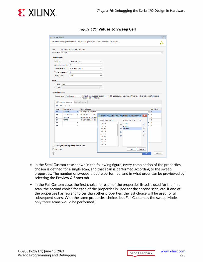
Figure 181: Values to Sweep Cell
• In the Semi Custom case shown in the following figure, every combination of the propertieschosen is defined for a single scan, and that scan is performed according to the sweepproperties. The number of sweeps that are performed, and in what order can be previewed byselecting the Preview & Scans tab.
• In the Full Custom case, the first choice for each of the properties listed is used for the firstscan, the second choice for each of the properties is used for the second scan, etc. If one ofthe properties has fewer choices than other properties, the last choice will be used for allsubsequent scans. With the same properties choices but Full Custom as the sweep Mode,only three scans would be performed.
Chapter 16: Debugging the Serial I/O Design in Hardware
UG908 (v2021.1) June 16, 2021 www.xilinx.comVivado Programming and Debugging 298Send Feedback
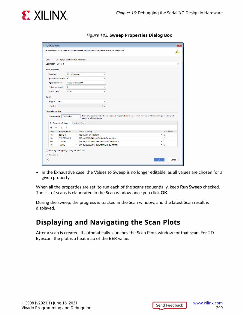
Figure 182: Sweep Properties Dialog Box
• In the Exhaustive case, the Values to Sweep is no longer editable, as all values are chosen for agiven property.
When all the properties are set, to run each of the scans sequentially, keep Run Sweep checked.The list of scans is elaborated in the Scan window once you click OK.
During the sweep, the progress is tracked in the Scan window, and the latest Scan result isdisplayed.
Displaying and Navigating the Scan PlotsAfter a scan is created, it automatically launches the Scan Plots window for that scan. For 2DEyescan, the plot is a heat map of the BER value.
Chapter 16: Debugging the Serial I/O Design in Hardware
UG908 (v2021.1) June 16, 2021 www.xilinx.comVivado Programming and Debugging 299Send Feedback
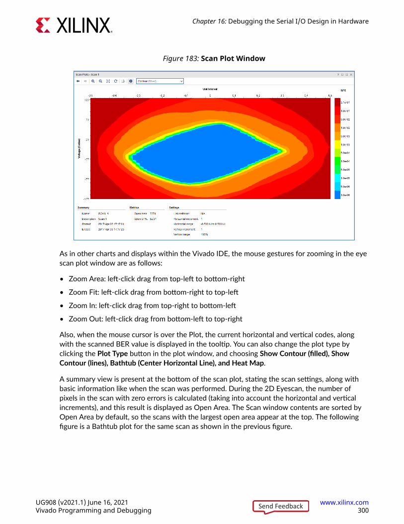
Figure 183: Scan Plot Window
As in other charts and displays within the Vivado IDE, the mouse gestures for zooming in the eyescan plot window are as follows:
• Zoom Area: left-click drag from top-left to bottom-right
• Zoom Fit: left-click drag from bottom-right to top-left
• Zoom In: left-click drag from top-right to bottom-left
• Zoom Out: left-click drag from bottom-left to top-right
Also, when the mouse cursor is over the Plot, the current horizontal and vertical codes, alongwith the scanned BER value is displayed in the tooltip. You can also change the plot type byclicking the Plot Type button in the plot window, and choosing Show Contour (filled), ShowContour (lines), Bathtub (Center Horizontal Line), and Heat Map.
A summary view is present at the bottom of the scan plot, stating the scan settings, along withbasic information like when the scan was performed. During the 2D Eyescan, the number ofpixels in the scan with zero errors is calculated (taking into account the horizontal and verticalincrements), and this result is displayed as Open Area. The Scan window contents are sorted byOpen Area by default, so the scans with the largest open area appear at the top. The followingfigure is a Bathtub plot for the same scan as shown in the previous figure.
Chapter 16: Debugging the Serial I/O Design in Hardware
UG908 (v2021.1) June 16, 2021 www.xilinx.comVivado Programming and Debugging 300Send Feedback
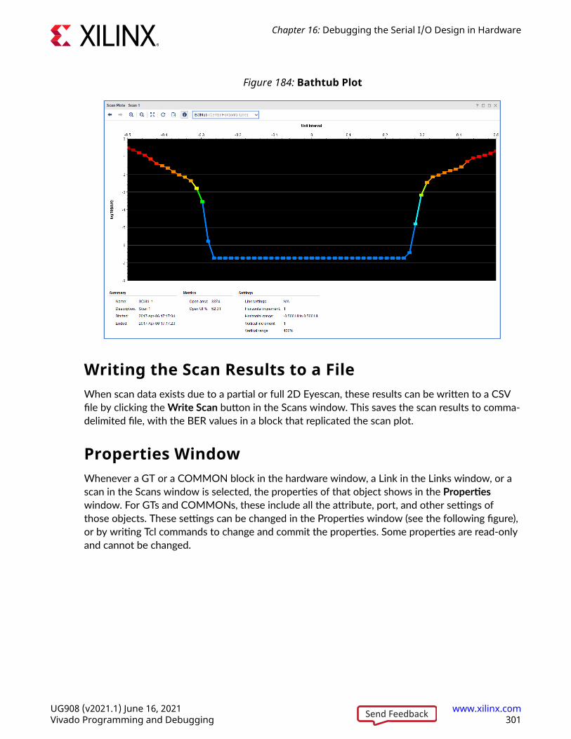
Figure 184: Bathtub Plot
Writing the Scan Results to a FileWhen scan data exists due to a partial or full 2D Eyescan, these results can be written to a CSVfile by clicking the Write Scan button in the Scans window. This saves the scan results to comma-delimited file, with the BER values in a block that replicated the scan plot.
Properties WindowWhenever a GT or a COMMON block in the hardware window, a Link in the Links window, or ascan in the Scans window is selected, the properties of that object shows in the Propertieswindow. For GTs and COMMONs, these include all the attribute, port, and other settings ofthose objects. These settings can be changed in the Properties window (see the following figure),or by writing Tcl commands to change and commit the properties. Some properties are read-onlyand cannot be changed.
Chapter 16: Debugging the Serial I/O Design in Hardware
UG908 (v2021.1) June 16, 2021 www.xilinx.comVivado Programming and Debugging 301Send Feedback
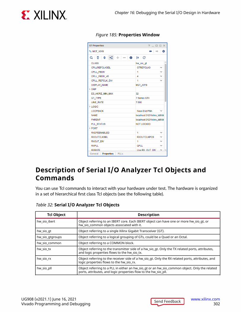
Figure 185: Properties Window
Description of Serial I/O Analyzer Tcl Objects andCommandsYou can use Tcl commands to interact with your hardware under test. The hardware is organizedin a set of hierarchical first class Tcl objects (see the following table).
Table 32: Serial I/O Analyzer Tcl Objects
Tcl Object Descriptionhw_sio_ibert Object referring to an IBERT core. Each IBERT object can have one or more hw_sio_gt, or
hw_sio_common objects associated with it.
hw_sio_gt Object referring to a single Xilinx Gigabit Transceiver (GT).
hw_sio_gtgroups Object referring to a logical grouping of GTs, could be a Quad or an Octal.
hw_sio_common Object referring to a COMMON block.
hw_sio_tx Object referring to the transmitter side of a hw_sio_gt. Only the TX related ports, attributes,and logic properties flows to the hw_sio_tx.
hw_sio_rx Object referring to the receiver side of a hw_sio_gt. Only the RX related ports, attributes, andlogic properties flows to the hw_sio_rx.
hw_sio_pll Object referring to a PLL in either an hw_sio_gt or an hw_sio_common object. Only the relatedports, attributes, and logic properties flow to the hw_sio_pll.
Chapter 16: Debugging the Serial I/O Design in Hardware
UG908 (v2021.1) June 16, 2021 www.xilinx.comVivado Programming and Debugging 302Send Feedback
Table 32: Serial I/O Analyzer Tcl Objects (cont'd)
Tcl Object Descriptionhw_sio_link Object referring to a link, a TX-RX pair.
A link can also consist of a TX only or an RX only.
hw_sio_linkgroup Object referring to a group of links.
hw_sio_scan Object referring to a margin analysis scan.
For more information about the Hardware Manager commands, run the help -categoryhardware Tcl command in the Tcl Console.
Description of Tcl Commands to Access Hardware
The following table contains descriptions of all Tcl commands used to interact with the IBERTcore.
IMPORTANT! Using the get_property or set_property command does not read or write information to/from the IBERT core. You must use the refresh_hw_sio and commit_hw_sio commands to read and writeinformation from/to the hardware, respectively.
Table 33: Descriptions of hw_server Tcl Commands
Tcl Command Descriptionrefresh_hw_sio Read the property values out of the provided object. Works for any hw_sio object that refers to
hardware.
commit_hw_sio Writes property changes to the hardware. Works for any hw_sio object that refers tohardware.
Description of hw_sio_link Tcl Commands
The following table contains descriptions of all Tcl commands used to interact with links.
Table 34: Descriptions of hw_sio_link Tcl Commands
Tcl Command Descriptioncreate_hw_sio_link Create an hw_sio_link object with the given hw_sio_rx and/or hw_sio_tx objects.
remove_hw_sio_link Deletes the given link.
get_hw_sio_links Get list of hw_sio_links for the given object.
Description of hw_sio_linkgroup Tcl Commands
The following table contains descriptions of all Tcl commands used to interact with linkgroups.
Chapter 16: Debugging the Serial I/O Design in Hardware
UG908 (v2021.1) June 16, 2021 www.xilinx.comVivado Programming and Debugging 303Send Feedback
Table 35: Descriptions of hw_sio_linkgroup Tcl Commands
Tcl Command Descriptioncreate_hw_sio_linkgroup Create an hw_sio_linkgroup object with the hw_sio_link objects.
remove_hw_sio_linkgroup Deletes the given linkgroup.
get_hw_sio_linkgroups Get list of hw_sio_linkgroups for the given object.
Description of hw_sio_scan Tcl Commands
The following table contains descriptions of all Tcl commands used to interact with scans.
Table 36: Descriptions of hw_sio_scan Tcl Commands
Tcl Command Descriptioncreate_hw_sio_scan Creates a scan object.
remove_hw_sio_scan Deletes a scan object.
run_hw_sio_scan Runs a scan.
stop_hw_sio_scan Stops a scan.
wait_on_hw_sio_scan Blocks the Tcl console prompt until a given run_hw_sio_scan operation is complete.
display_hw_sio_scan Displays a partial or complete scan in the Scan Plot.
write_hw_sio_scan Writes the scan data to a file.
read_hw_sio_scan Reads scan data from a file into a scan object.
get_hw_sio_scans Get a list of hw_sio_scan objects.
Description of Tcl Commands to Get Objects
The following table contains descriptions of all Tcl commands used to get serial I/O objects.
Table 37: Descriptions of Tcl Commands to Get Objects
Tcl Command Descriptionget_hw_sio_iberts Get list of IBERT objects.
get_hw_sio_gts Get list of GTs.
get_hw_sio_commons Get list of COMMON blocks.
get_hw_sio_txs Get list of transmitters.
get_hw_sio_rxs Get list of receivers.
get_hw_sio_plls Get list of PLLs.
get_hw_sio_links Get list of links.
get_hw_sio_linkgroups Get list of linkgroups.
get_hw_sio_scans Get list of scans.
Chapter 16: Debugging the Serial I/O Design in Hardware
UG908 (v2021.1) June 16, 2021 www.xilinx.comVivado Programming and Debugging 304Send Feedback
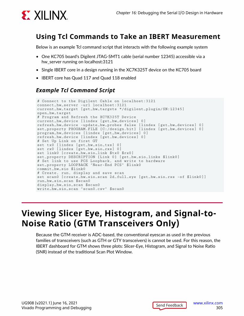
Using Tcl Commands to Take an IBERT MeasurementBelow is an example Tcl command script that interacts with the following example system
• One KC705 board's Digilent JTAG-SMT1 cable (serial number 12345) accessible via ahw_server running on localhost:3121
• Single IBERT core in a design running in the XC7K325T device on the KC705 board
• IBERT core has Quad 117 and Quad 118 enabled
Example Tcl Command Script
# Connect to the Digilent Cable on localhost:3121connect_hw_server -url localhost:3121current_hw_target [get_hw_targets */digilent_plugin/SN:12345]open_hw_target# Program and Refresh the XC7K325T Devicecurrent_hw_device [lindex [get_hw_devices] 0]refresh_hw_device -update_hw_probes false [lindex [get_hw_devices] 0]set_property PROGRAM.FILE {C:/design.bit} [lindex [get_hw_devices] 0]program_hw_devices [lindex [get_hw_devices] 0]refresh_hw_device [lindex [get_hw_devices] 0]# Set Up Link on first GT set tx0 [lindex [get_hw_sio_txs] 0]set rx0 [lindex [get_hw_sio_rxs] 0]set link0 [create_hw_sio_link $tx0 $rx0]set_property DESCRIPTION {Link 0} [get_hw_sio_links $link0]# Set link to use PCS Loopback, and write to hardwareset_property LOOPBACK "Near-End PCS" $link0commit_hw_sio $link0# Create, run, display and save scanset scan0 [create_hw_sio_scan 2d_full_eye [get_hw_sio_rxs -of $link0]]run_hw_sio_scan $scan0display_hw_sio_scan $scan0write_hw_sio_scan "scan0.csv" $scan0
Viewing Slicer Eye, Histogram, and Signal-to-Noise Ratio (GTM Transceivers Only)
Because the GTM receiver is ADC-based, the conventional eyescan as used in the previousfamilies of transceivers (such as GTH or GTY transceivers) is cannot be used. For this reason, theIBERT dashboard for GTM shows three plots: Slicer-Eye, Histogram, and Signal to Noise Ratio(SNR) instead of the traditional Scan Plot Window.
Chapter 16: Debugging the Serial I/O Design in Hardware
UG908 (v2021.1) June 16, 2021 www.xilinx.comVivado Programming and Debugging 305Send Feedback
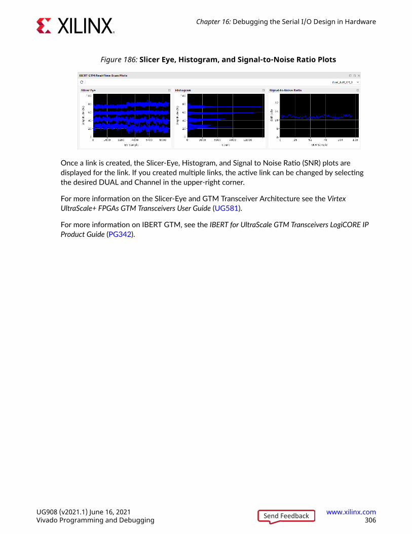
Figure 186: Slicer Eye, Histogram, and Signal-to-Noise Ratio Plots
Once a link is created, the Slicer-Eye, Histogram, and Signal to Noise Ratio (SNR) plots aredisplayed for the link. If you created multiple links, the active link can be changed by selectingthe desired DUAL and Channel in the upper-right corner.
For more information on the Slicer-Eye and GTM Transceiver Architecture see the VirtexUltraScale+ FPGAs GTM Transceivers User Guide (UG581).
For more information on IBERT GTM, see the IBERT for UltraScale GTM Transceivers LogiCORE IPProduct Guide (PG342).
Chapter 16: Debugging the Serial I/O Design in Hardware
UG908 (v2021.1) June 16, 2021 www.xilinx.comVivado Programming and Debugging 306Send Feedback
Appendix A
Device Configuration Bitstream orPDI Settings
7 Series Bitstream SettingsThe device configuration settings for 7 series devices available for use with the set_property<Setting> <Value> [current_design] Vivado® tool Tcl command are shown in thefollowing table.
Note: Bitstream settings for BPI are not valid for Spartan®-7 devices.
Table 38: 7 Series Bitstream Settings
Setting DefaultValue
PossibleValues Description
BITSTREAM.CONFIG.BPI_1ST_READ_CYCLE
1 1, 2, 3, 4 Helps synchronize BPI configuration with the timing ofpage mode operations in flash devices. It allows you toset the cycle number for a valid read of the first page.The BPI_page_size must be set to 4 or 8 for this option tobe available.
BITSTREAM.CONFIG.BPI_PAGE_SIZE
1 1, 4, 8 For BPI configuration, this option lets you specify thepage size which corresponds to the number of readsrequired per page of flash memory.
BITSTREAM.CONFIG.BPI_SYNC_MODE
Disable Disable,Type1, Type2
Sets the BPI synchronous configuration mode fordifferent types of BPI flash devices.Disable (the default) disables the synchronousconfiguration mode.Type1 enables the synchronous configuration mode andsettings to support the Micron G18(F) family.Type2 enables the synchronous configuration mode andsettings to support the Micron (Numonyx) P30 and P33families.
BITSTREAM.CONFIG. CCLKPIN Pullup Pullup,Pullnone
Adds an internal pull-up to the Cclk pin. The Pullnonesetting disables the pullup.
BITSTREAM.CONFIG.CONFIGFALLBACK
Disable Disable,Enable
Enables or disables the loading of a default bitstreamwhen a configuration attempt fails.If the MultiBoot solution settingBITSTREAM.CONFIG.NEXT_CONFIG_ADDR is used thenthe BITSTREAM.CONFIG.FALLBACK setting will beenabled.Fallback MultiBoot is not supported in Virtex-7 HTdevices.
Appendix A: Device Configuration Bitstream or PDI Settings
UG908 (v2021.1) June 16, 2021 www.xilinx.comVivado Programming and Debugging 307Send Feedback
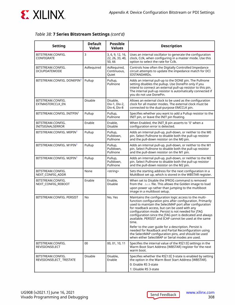
Table 38: 7 Series Bitstream Settings (cont'd)
Setting DefaultValue
PossibleValues Description
BITSTREAM.CONFIG.CONFIGRATE
3 3, 6, 9, 12, 16,22, 26, 33, 40,50, 66
Uses an internal oscillator to generate the configurationclock, Cclk, when configuring in a master mode. Use thisoption to select the rate for Cclk.
BITSTREAM.CONFIG.DCIUPDATEMODE
AsRequired AsRequired,Continuous,Quiet
Controls how often the Digitally Controlled Impedancecircuit attempts to update the impedance match for DCIIOSTANDARDs.
BITSTREAM.CONFIG. DONEPIN1 Pullup Pullup,Pullnone
Adds an internal pull-up to the DONE pin. The Pullnonesetting disables the pullup. Use DonePin only if youintend to connect an external pull-up resistor to this pin.The internal pull-up resistor is automatically connected ifyou do not use DonePin.
BITSTREAM.CONFIG.EXTMASTERCCLK_EN
Disable Disable,Div-1, Div-2,Div-4, Div-8
Allows an external clock to be used as the configurationclock for all master modes. The external clock must beconnected to the dual-purpose EMCCLK pin.
BITSTREAM.CONFIG. INITPIN1 Pullup Pullup,Pullnone
Specifies whether you want to add a Pullup resistor to theINIT pin, or leave the INIT pin floating.
BITSTREAM.CONFIG.INITSIGNALSERROR
Enable Enable,Disable
When Enabled, the INIT_B pin asserts to '0' when aconfiguration error is detected.
BITSTREAM.CONFIG. M0PIN1 Pullup Pullup,Pulldown,Pullnone
Adds an internal pull-up, pull-down, or neither to the M0pin. Select Pullnone to disable both the pull-up resistorand the pull-down resistor on the M0 pin.
BITSTREAM.CONFIG. M1PIN1 Pullup Pullup,Pulldown,Pullnone
Adds an internal pull-up, pull-down, or neither to the M1pin. Select Pullnone to disable both the pull-up resistorand the pull-down resistor on the M1 pin.
BITSTREAM.CONFIG. M2PIN1 Pullup Pullup,Pulldown,Pullnone
Adds an internal pull-up, pull-down, or neither to the M2pin. Select Pullnone to disable both the pull-up resistorand the pull-down resistor on the M2 pin.
BITSTREAM.CONFIG.NEXT_CONFIG_ADDR
None <string> Sets the starting address for the next configuration in aMultiBoot set up, which is stored in the WBSTAR register.
BITSTREAM.CONFIG.NEXT_CONFIG_REBOOT
Enable Enable,Disable
When set to Disable the IPROG command is removedfrom the .bit file. This allows the Golden image to loadupon power up rather than jumping to the multibootimage in a multiboot setup.
BITSTREAM.CONFIG. PERSIST No No, Yes Maintains the configuration logic access to the multi-function configuration pins after configuration. Primarilyused to maintain the SelectMAP port after configurationfor readback access, but can be used with anyconfiguration mode. Persist is not needed for JTAGconfiguration since the JTAG port is dedicated and alwaysavailable. PERSIST and ICAP cannot be used at the sametime.Refer to the user guide for a description. Persist isneeded for Readback and Partial Reconfiguration usingthe SelectMAP configuration pins, and should be usedwhen either SelectMAP or Serial modes are used.
BITSTREAM.CONFIG.REVISIONSELECT
00 00, 01, 10, 11 Specifies the internal value of the RS[1:0] settings in theWarm Boot Start Address (WBSTAR) register for the nextwarm boot.
BITSTREAM.CONFIG.REVISIONSELECT_ TRISTATE
Disable Disable,Enable
Specifies whether the RS[1:0] 3-state is enabled by settingthe option in the Warm Boot Start Address (WBSTAR).0: Enable RS 3-state1: Disable RS 3-state
Appendix A: Device Configuration Bitstream or PDI Settings
UG908 (v2021.1) June 16, 2021 www.xilinx.comVivado Programming and Debugging 308Send Feedback
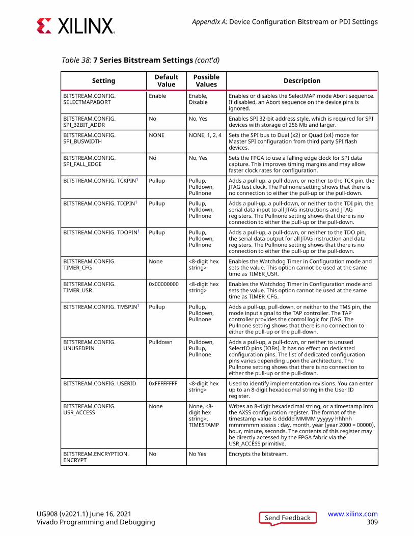
Table 38: 7 Series Bitstream Settings (cont'd)
Setting DefaultValue
PossibleValues Description
BITSTREAM.CONFIG.SELECTMAPABORT
Enable Enable,Disable
Enables or disables the SelectMAP mode Abort sequence.If disabled, an Abort sequence on the device pins isignored.
BITSTREAM.CONFIG.SPI_32BIT_ADDR
No No, Yes Enables SPI 32-bit address style, which is required for SPIdevices with storage of 256 Mb and larger.
BITSTREAM.CONFIG.SPI_BUSWIDTH
NONE NONE, 1, 2, 4 Sets the SPI bus to Dual (x2) or Quad (x4) mode forMaster SPI configuration from third party SPI flashdevices.
BITSTREAM.CONFIG.SPI_FALL_EDGE
No No, Yes Sets the FPGA to use a falling edge clock for SPI datacapture. This improves timing margins and may allowfaster clock rates for configuration.
BITSTREAM.CONFIG. TCKPIN1 Pullup Pullup,Pulldown,Pullnone
Adds a pull-up, a pull-down, or neither to the TCK pin, theJTAG test clock. The Pullnone setting shows that there isno connection to either the pull-up or the pull-down.
BITSTREAM.CONFIG. TDIPIN1 Pullup Pullup,Pulldown,Pullnone
Adds a pull-up, a pull-down, or neither to the TDI pin, theserial data input to all JTAG instructions and JTAGregisters. The Pullnone setting shows that there is noconnection to either the pull-up or the pull-down.
BITSTREAM.CONFIG. TDOPIN1 Pullup Pullup,Pulldown,Pullnone
Adds a pull-up, a pull-down, or neither to the TDO pin,the serial data output for all JTAG instruction and dataregisters. The Pullnone setting shows that there is noconnection to either the pull-up or the pull-down.
BITSTREAM.CONFIG.TIMER_CFG
None <8-digit hexstring>
Enables the Watchdog Timer in Configuration mode andsets the value. This option cannot be used at the sametime as TIMER_USR.
BITSTREAM.CONFIG.TIMER_USR
0x00000000 <8-digit hexstring>
Enables the Watchdog Timer in Configuration mode andsets the value. This option cannot be used at the sametime as TIMER_CFG.
BITSTREAM.CONFIG. TMSPIN1 Pullup Pullup,Pulldown,Pullnone
Adds a pull-up, pull-down, or neither to the TMS pin, themode input signal to the TAP controller. The TAPcontroller provides the control logic for JTAG. ThePullnone setting shows that there is no connection toeither the pull-up or the pull-down.
BITSTREAM.CONFIG.UNUSEDPIN
Pulldown Pulldown,Pullup,Pullnone
Adds a pull-up, a pull-down, or neither to unusedSelectIO pins (IOBs). It has no effect on dedicatedconfiguration pins. The list of dedicated configurationpins varies depending upon the architecture. ThePullnone setting shows that there is no connection toeither the pull-up or the pull-down.
BITSTREAM.CONFIG. USERID 0xFFFFFFFF <8-digit hexstring>
Used to identify implementation revisions. You can enterup to an 8-digit hexadecimal string in the User IDregister.
BITSTREAM.CONFIG.USR_ACCESS
None None, <8-digit hexstring>,TIMESTAMP
Writes an 8-digit hexadecimal string, or a timestamp intothe AXSS configuration register. The format of thetimestamp value is ddddd MMMM yyyyyy hhhhhmmmmmm ssssss : day, month, year (year 2000 = 00000),hour, minute, seconds. The contents of this register maybe directly accessed by the FPGA fabric via theUSR_ACCESS primitive.
BITSTREAM.ENCRYPTION.ENCRYPT
No No Yes Encrypts the bitstream.
Appendix A: Device Configuration Bitstream or PDI Settings
UG908 (v2021.1) June 16, 2021 www.xilinx.comVivado Programming and Debugging 309Send Feedback
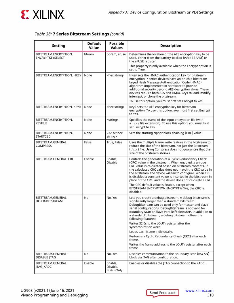
Table 38: 7 Series Bitstream Settings (cont'd)
Setting DefaultValue
PossibleValues Description
BITSTREAM.ENCRYPTION.ENCRYPTKEYSELECT
bbram bbram, efuse Determines the location of the AES encryption key to beused, either from the battery-backed RAM (BBRAM) orthe eFUSE register.This property is only available when the Encrypt option isset to True.
BITSTREAM.ENCRYPTION. HKEY None <hex string> HKey sets the HMAC authentication key for bitstreamencryption. 7 series devices have an on-chip bitstream-keyed Hash Message Authentication Code (HMAC)algorithm implemented in hardware to provideadditional security beyond AES decryption alone. Thesedevices require both AES and HMAC keys to load, modify,intercept, or clone the bitstream.To use this option, you must first set Encrypt to Yes.
BITSTREAM.ENCRYPTION. KEY0 None <hex string> Key0 sets the AES encryption key for bitstreamencryption. To use this option, you must first set Encryptto Yes.
BITSTREAM.ENCRYPTION.KEYFILE
None <string> Specifies the name of the input encryption file (witha .nky file extension). To use this option, you must firstset Encrypt to Yes.
BITSTREAM.ENCRYPTION.STARTCBC
None <32-bit hexstring>
Sets the starting cipher block chaining (CBC) value.
BITSTREAM.GENERAL.COMPRESS
False True, False Uses the multiple frame write feature in the bitstream toreduce the size of the bitstream, not just the Bitstream(.bit) file. Using Compress does not guarantee that thesize of the bitstream shrinks.
BITSTREAM.GENERAL. CRC Enable Enable,Disable
Controls the generation of a Cyclic Redundancy Check(CRC) value in the bitstream. When enabled, a uniqueCRC value is calculated based on bitstream contents. Ifthe calculated CRC value does not match the CRC value inthe bitstream, the device will fail to configure. When CRCis disabled a constant value is inserted in the bitstream inplace of the CRC, and the device does not calculate a CRC.The CRC default value is Enable, except whenBITSTREAM.ENCRYPTION.ENCRYPT is Yes, the CRC isdisabled.
BITSTREAM.GENERAL.DEBUGBITSTREAM
No No, Yes Lets you create a debug bitstream. A debug bitstream issignificantly larger than a standard bitstream.DebugBitstream can be used only for master and slaveserial configurations. DebugBitstream is not valid forBoundary Scan or Slave Parallel/SelectMAP. In addition toa standard bitstream, a debug bitstream offers thefollowing features:Writes 32 0s to the LOUT register after thesynchronization word.Loads each frame individually.Performs a Cyclic Redundancy Check (CRC) after eachframe.Writes the frame address to the LOUT register after eachframe.
BITSTREAM.GENERAL.DISABLE_JTAG
No No, Yes Disables communication to the Boundary Scan (BSCAN)block via JTAG after configuration.
BITSTREAM.GENERAL.JTAG_XADC
Enable Enable,Disable,StatusOnly
Enables or disables the JTAG connection to the XADC.
Appendix A: Device Configuration Bitstream or PDI Settings
UG908 (v2021.1) June 16, 2021 www.xilinx.comVivado Programming and Debugging 310Send Feedback
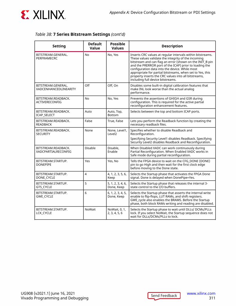
Table 38: 7 Series Bitstream Settings (cont'd)
Setting DefaultValue
PossibleValues Description
BITSTREAM.GENERAL.PERFRAMECRC
No No, Yes Inserts CRC values at regular intervals within bitstreams.These values validate the integrity of the incomingbitstream and can flag an error (shown on the INIT_B pinand the PRERROR port of the ICAP) prior to loading theconfiguration data into the device. While mostappropriate for partial bitstreams, when set to Yes, thisproperty inserts the CRC values into all bitstreams,including full device bitstreams.
BITSTREAM.GENERAL.XADCENHANCEDLINEARITY
Off Off, On Disables some built-in digital calibration features thatmake INL look worse than the actual analogperformance.
BITSTREAM.READBACK.ACTIVERECONFIG
No No, Yes Prevents the assertions of GHIGH and GSR duringconfiguration. This is required for the active partialreconfiguration enhancement features.
BITSTREAM.READBACK.ICAP_SELECT
Auto Auto, Top,Bottom
Selects between the top and bottom ICAP ports.
BITSTREAM.READBACK.READBACK
False True, False Lets you perform the Readback function by creating thenecessary readback files.
BITSTREAM.READBACK.SECURITY
None None, Level1,Level2
Specifies whether to disable Readback andReconfiguration.Specifying Security Level1 disables Readback. SpecifyingSecurity Level2 disables Readback and Reconfiguration.
BITSTREAM.READBACK.XADCPARTIALRECONFIG
Disable Disable,Enable
When Disabled XADC can work continuously duringPartial Reconfiguration. When Enabled XADC works inSafe mode during partial reconfiguration.
BITSTREAM.STARTUP.DONEPIPE
Yes Yes, No Tells the FPGA device to wait on the CFG_DONE (DONE)pin to go High and then wait for the first clock edgebefore moving to the Done state.
BITSTREAM.STARTUP.DONE_CYCLE
4 4, 1, 2, 3, 5, 6,Keep
Selects the Startup phase that activates the FPGA Donesignal. Done is delayed when DonePipe=Yes.
BITSTREAM.STARTUP.GTS_CYCLE
5 5, 1, 2, 3, 4, 6,Done, Keep
Selects the Startup phase that releases the internal 3-state control to the I/O buffers.
BITSTREAM.STARTUP.GWE_CYCLE
6 6, 1, 2, 3, 4, 5,Done, Keep
Selects the Startup phase that asserts the internal writeenable to flip-flops, LUT RAMs, and shift registers.GWE_cycle also enables the BRAMS. Before the Startupphase, both block RAMs writing and reading are disabled.
BITSTREAM.STARTUP.LCK_CYCLE
NoWait NoWait, 0, 1,2, 3, 4, 5, 6
Selects the Startup phase to wait until DLLs/ DCMs/PLLslock. If you select NoWait, the Startup sequence does notwait for DLLs/DCMs/PLLs to lock.
Appendix A: Device Configuration Bitstream or PDI Settings
UG908 (v2021.1) June 16, 2021 www.xilinx.comVivado Programming and Debugging 311Send Feedback
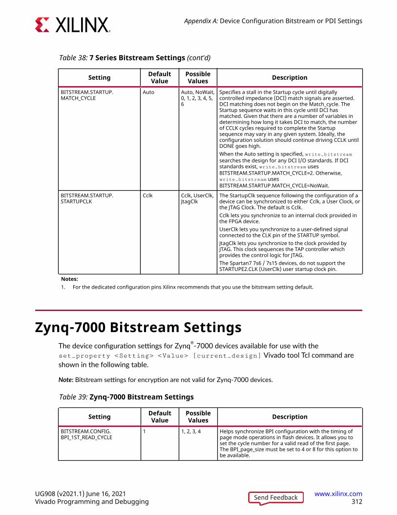
Table 38: 7 Series Bitstream Settings (cont'd)
Setting DefaultValue
PossibleValues Description
BITSTREAM.STARTUP.MATCH_CYCLE
Auto Auto, NoWait,0, 1, 2, 3, 4, 5,6
Specifies a stall in the Startup cycle until digitallycontrolled impedance (DCI) match signals are asserted.DCI matching does not begin on the Match_cycle. TheStartup sequence waits in this cycle until DCI hasmatched. Given that there are a number of variables indetermining how long it takes DCI to match, the numberof CCLK cycles required to complete the Startupsequence may vary in any given system. Ideally, theconfiguration solution should continue driving CCLK untilDONE goes high.When the Auto setting is specified, write_bitstreamsearches the design for any DCI I/O standards. If DCIstandards exist, write_bitstream usesBITSTREAM.STARTUP.MATCH_CYCLE=2. Otherwise,write_bitstream usesBITSTREAM.STARTUP.MATCH_CYCLE=NoWait.
BITSTREAM.STARTUP.STARTUPCLK
Cclk Cclk, UserClk,JtagClk
The StartupClk sequence following the configuration of adevice can be synchronized to either Cclk, a User Clock, orthe JTAG Clock. The default is Cclk.Cclk lets you synchronize to an internal clock provided inthe FPGA device.UserClk lets you synchronize to a user-defined signalconnected to the CLK pin of the STARTUP symbol.JtagClk lets you synchronize to the clock provided byJTAG. This clock sequences the TAP controller whichprovides the control logic for JTAG.The Spartan7 7s6 / 7s15 devices, do not support theSTARTUPE2.CLK (UserClk) user startup clock pin.
Notes:1. For the dedicated configuration pins Xilinx recommends that you use the bitstream setting default.
Zynq-7000 Bitstream SettingsThe device configuration settings for Zynq®-7000 devices available for use with theset_property <Setting> <Value> [current_design] Vivado tool Tcl command areshown in the following table.
Note: Bitstream settings for encryption are not valid for Zynq-7000 devices.
Table 39: Zynq-7000 Bitstream Settings
Setting DefaultValue
PossibleValues Description
BITSTREAM.CONFIG.BPI_1ST_READ_CYCLE
1 1, 2, 3, 4 Helps synchronize BPI configuration with the timing ofpage mode operations in flash devices. It allows you toset the cycle number for a valid read of the first page.The BPI_page_size must be set to 4 or 8 for this option tobe available.
Appendix A: Device Configuration Bitstream or PDI Settings
UG908 (v2021.1) June 16, 2021 www.xilinx.comVivado Programming and Debugging 312Send Feedback
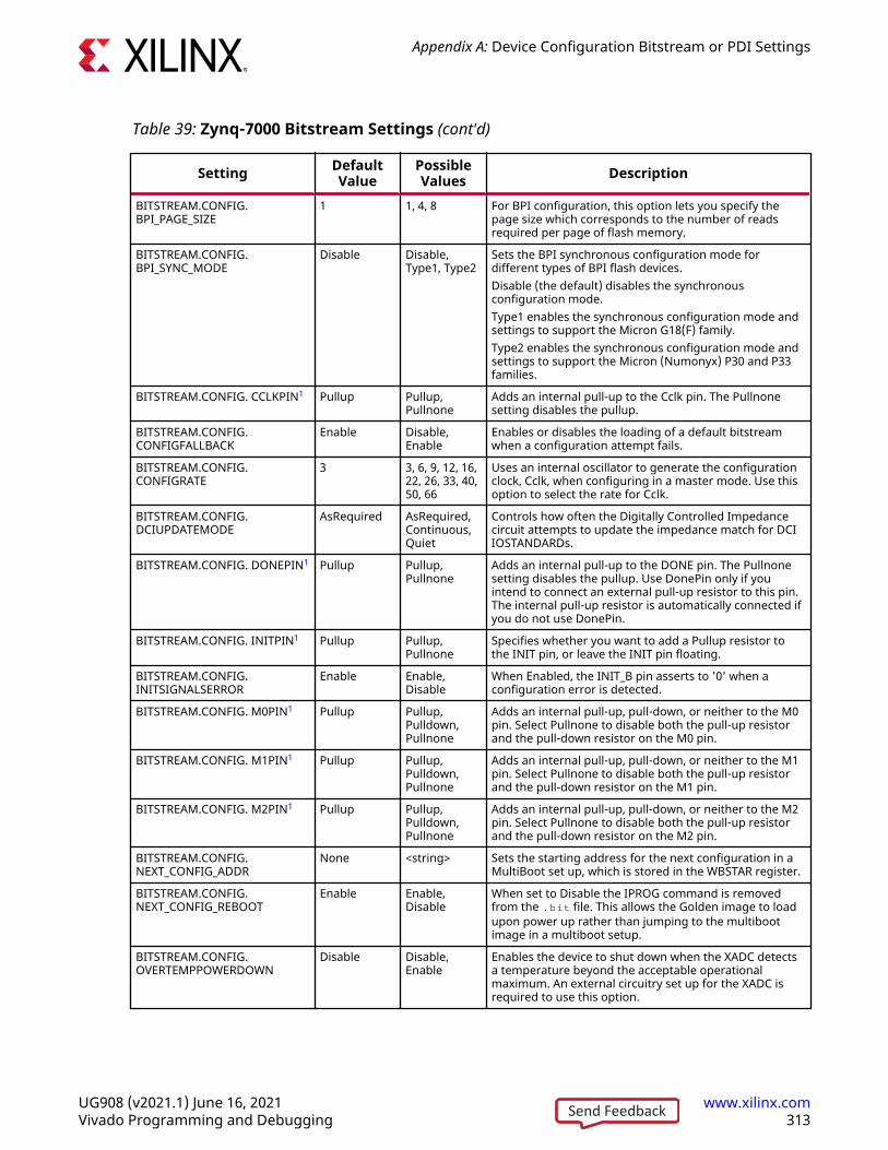
Table 39: Zynq-7000 Bitstream Settings (cont'd)
Setting DefaultValue
PossibleValues Description
BITSTREAM.CONFIG.BPI_PAGE_SIZE
1 1, 4, 8 For BPI configuration, this option lets you specify thepage size which corresponds to the number of readsrequired per page of flash memory.
BITSTREAM.CONFIG.BPI_SYNC_MODE
Disable Disable,Type1, Type2
Sets the BPI synchronous configuration mode fordifferent types of BPI flash devices.Disable (the default) disables the synchronousconfiguration mode.Type1 enables the synchronous configuration mode andsettings to support the Micron G18(F) family.Type2 enables the synchronous configuration mode andsettings to support the Micron (Numonyx) P30 and P33families.
BITSTREAM.CONFIG. CCLKPIN1 Pullup Pullup,Pullnone
Adds an internal pull-up to the Cclk pin. The Pullnonesetting disables the pullup.
BITSTREAM.CONFIG.CONFIGFALLBACK
Enable Disable,Enable
Enables or disables the loading of a default bitstreamwhen a configuration attempt fails.
BITSTREAM.CONFIG.CONFIGRATE
3 3, 6, 9, 12, 16,22, 26, 33, 40,50, 66
Uses an internal oscillator to generate the configurationclock, Cclk, when configuring in a master mode. Use thisoption to select the rate for Cclk.
BITSTREAM.CONFIG.DCIUPDATEMODE
AsRequired AsRequired,Continuous,Quiet
Controls how often the Digitally Controlled Impedancecircuit attempts to update the impedance match for DCIIOSTANDARDs.
BITSTREAM.CONFIG. DONEPIN1 Pullup Pullup,Pullnone
Adds an internal pull-up to the DONE pin. The Pullnonesetting disables the pullup. Use DonePin only if youintend to connect an external pull-up resistor to this pin.The internal pull-up resistor is automatically connected ifyou do not use DonePin.
BITSTREAM.CONFIG. INITPIN1 Pullup Pullup,Pullnone
Specifies whether you want to add a Pullup resistor tothe INIT pin, or leave the INIT pin floating.
BITSTREAM.CONFIG.INITSIGNALSERROR
Enable Enable,Disable
When Enabled, the INIT_B pin asserts to '0' when aconfiguration error is detected.
BITSTREAM.CONFIG. M0PIN1 Pullup Pullup,Pulldown,Pullnone
Adds an internal pull-up, pull-down, or neither to the M0pin. Select Pullnone to disable both the pull-up resistorand the pull-down resistor on the M0 pin.
BITSTREAM.CONFIG. M1PIN1 Pullup Pullup,Pulldown,Pullnone
Adds an internal pull-up, pull-down, or neither to the M1pin. Select Pullnone to disable both the pull-up resistorand the pull-down resistor on the M1 pin.
BITSTREAM.CONFIG. M2PIN1 Pullup Pullup,Pulldown,Pullnone
Adds an internal pull-up, pull-down, or neither to the M2pin. Select Pullnone to disable both the pull-up resistorand the pull-down resistor on the M2 pin.
BITSTREAM.CONFIG.NEXT_CONFIG_ADDR
None <string> Sets the starting address for the next configuration in aMultiBoot set up, which is stored in the WBSTAR register.
BITSTREAM.CONFIG.NEXT_CONFIG_REBOOT
Enable Enable,Disable
When set to Disable the IPROG command is removedfrom the .bit file. This allows the Golden image to loadupon power up rather than jumping to the multibootimage in a multiboot setup.
BITSTREAM.CONFIG.OVERTEMPPOWERDOWN
Disable Disable,Enable
Enables the device to shut down when the XADC detectsa temperature beyond the acceptable operationalmaximum. An external circuitry set up for the XADC isrequired to use this option.
Appendix A: Device Configuration Bitstream or PDI Settings
UG908 (v2021.1) June 16, 2021 www.xilinx.comVivado Programming and Debugging 313Send Feedback
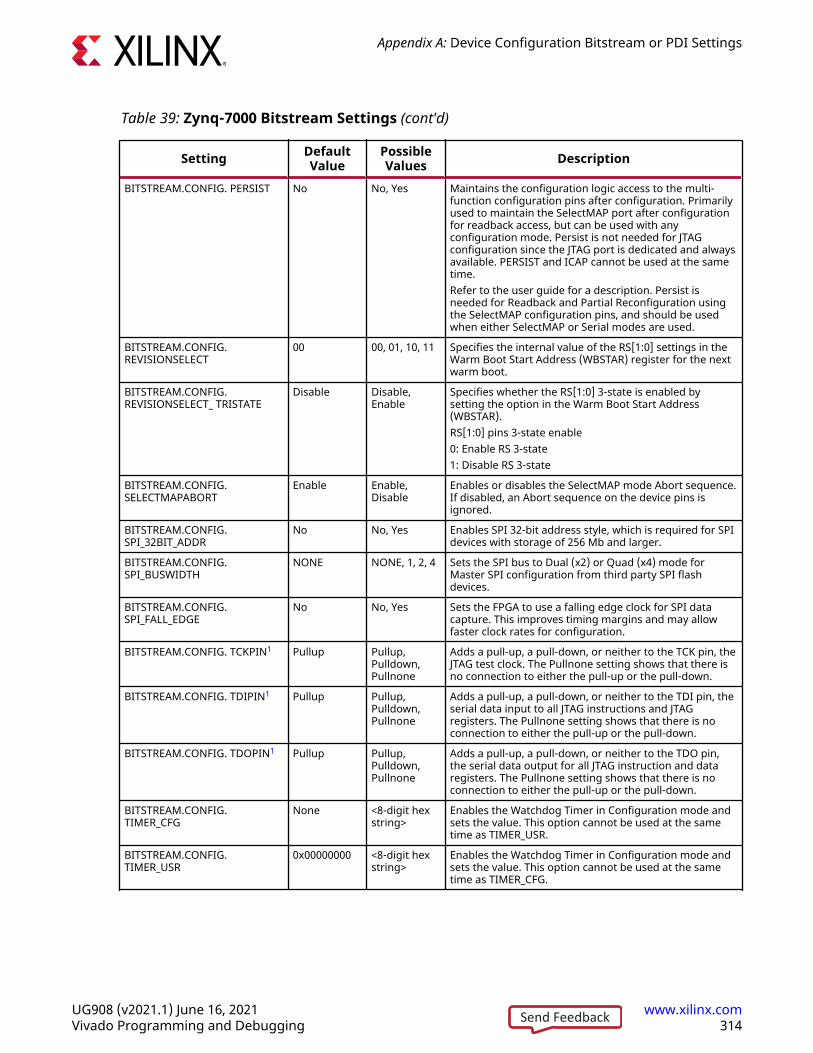
Table 39: Zynq-7000 Bitstream Settings (cont'd)
Setting DefaultValue
PossibleValues Description
BITSTREAM.CONFIG. PERSIST No No, Yes Maintains the configuration logic access to the multi-function configuration pins after configuration. Primarilyused to maintain the SelectMAP port after configurationfor readback access, but can be used with anyconfiguration mode. Persist is not needed for JTAGconfiguration since the JTAG port is dedicated and alwaysavailable. PERSIST and ICAP cannot be used at the sametime.Refer to the user guide for a description. Persist isneeded for Readback and Partial Reconfiguration usingthe SelectMAP configuration pins, and should be usedwhen either SelectMAP or Serial modes are used.
BITSTREAM.CONFIG.REVISIONSELECT
00 00, 01, 10, 11 Specifies the internal value of the RS[1:0] settings in theWarm Boot Start Address (WBSTAR) register for the nextwarm boot.
BITSTREAM.CONFIG.REVISIONSELECT_ TRISTATE
Disable Disable,Enable
Specifies whether the RS[1:0] 3-state is enabled bysetting the option in the Warm Boot Start Address(WBSTAR).RS[1:0] pins 3-state enable0: Enable RS 3-state1: Disable RS 3-state
BITSTREAM.CONFIG.SELECTMAPABORT
Enable Enable,Disable
Enables or disables the SelectMAP mode Abort sequence.If disabled, an Abort sequence on the device pins isignored.
BITSTREAM.CONFIG.SPI_32BIT_ADDR
No No, Yes Enables SPI 32-bit address style, which is required for SPIdevices with storage of 256 Mb and larger.
BITSTREAM.CONFIG.SPI_BUSWIDTH
NONE NONE, 1, 2, 4 Sets the SPI bus to Dual (x2) or Quad (x4) mode forMaster SPI configuration from third party SPI flashdevices.
BITSTREAM.CONFIG.SPI_FALL_EDGE
No No, Yes Sets the FPGA to use a falling edge clock for SPI datacapture. This improves timing margins and may allowfaster clock rates for configuration.
BITSTREAM.CONFIG. TCKPIN1 Pullup Pullup,Pulldown,Pullnone
Adds a pull-up, a pull-down, or neither to the TCK pin, theJTAG test clock. The Pullnone setting shows that there isno connection to either the pull-up or the pull-down.
BITSTREAM.CONFIG. TDIPIN1 Pullup Pullup,Pulldown,Pullnone
Adds a pull-up, a pull-down, or neither to the TDI pin, theserial data input to all JTAG instructions and JTAGregisters. The Pullnone setting shows that there is noconnection to either the pull-up or the pull-down.
BITSTREAM.CONFIG. TDOPIN1 Pullup Pullup,Pulldown,Pullnone
Adds a pull-up, a pull-down, or neither to the TDO pin,the serial data output for all JTAG instruction and dataregisters. The Pullnone setting shows that there is noconnection to either the pull-up or the pull-down.
BITSTREAM.CONFIG.TIMER_CFG
None <8-digit hexstring>
Enables the Watchdog Timer in Configuration mode andsets the value. This option cannot be used at the sametime as TIMER_USR.
BITSTREAM.CONFIG.TIMER_USR
0x00000000 <8-digit hexstring>
Enables the Watchdog Timer in Configuration mode andsets the value. This option cannot be used at the sametime as TIMER_CFG.
Appendix A: Device Configuration Bitstream or PDI Settings
UG908 (v2021.1) June 16, 2021 www.xilinx.comVivado Programming and Debugging 314Send Feedback
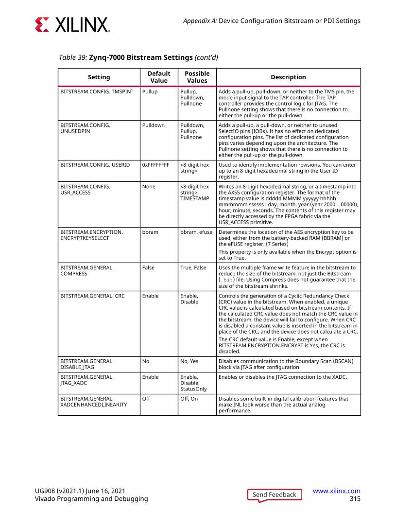
Table 39: Zynq-7000 Bitstream Settings (cont'd)
Setting DefaultValue
PossibleValues Description
BITSTREAM.CONFIG. TMSPIN1 Pullup Pullup,Pulldown,Pullnone
Adds a pull-up, pull-down, or neither to the TMS pin, themode input signal to the TAP controller. The TAPcontroller provides the control logic for JTAG. ThePullnone setting shows that there is no connection toeither the pull-up or the pull-down.
BITSTREAM.CONFIG.UNUSEDPIN
Pulldown Pulldown,Pullup,Pullnone
Adds a pull-up, a pull-down, or neither to unusedSelectIO pins (IOBs). It has no effect on dedicatedconfiguration pins. The list of dedicated configurationpins varies depending upon the architecture. ThePullnone setting shows that there is no connection toeither the pull-up or the pull-down.
BITSTREAM.CONFIG. USERID 0xFFFFFFFF <8-digit hexstring>
Used to identify implementation revisions. You can enterup to an 8-digit hexadecimal string in the User IDregister.
BITSTREAM.CONFIG.USR_ACCESS
None <8-digit hexstring>,TIMESTAMP
Writes an 8-digit hexadecimal string, or a timestamp intothe AXSS configuration register. The format of thetimestamp value is ddddd MMMM yyyyyy hhhhhmmmmmm ssssss : day, month, year (year 2000 = 00000),hour, minute, seconds. The contents of this register maybe directly accessed by the FPGA fabric via theUSR_ACCESS primitive.
BITSTREAM.ENCRYPTION.ENCRYPTKEYSELECT
bbram bbram, efuse Determines the location of the AES encryption key to beused, either from the battery-backed RAM (BBRAM) orthe eFUSE register. (7 Series)This property is only available when the Encrypt option isset to True.
BITSTREAM.GENERAL.COMPRESS
False True, False Uses the multiple frame write feature in the bitstream toreduce the size of the bitstream, not just the Bitstream(.bit) file. Using Compress does not guarantee that thesize of the bitstream shrinks.
BITSTREAM.GENERAL. CRC Enable Enable,Disable
Controls the generation of a Cyclic Redundancy Check(CRC) value in the bitstream. When enabled, a uniqueCRC value is calculated based on bitstream contents. Ifthe calculated CRC value does not match the CRC value inthe bitstream, the device will fail to configure. When CRCis disabled a constant value is inserted in the bitstream inplace of the CRC, and the device does not calculate a CRC.The CRC default value is Enable, except whenBITSTREAM.ENCRYPTION.ENCRYPT is Yes, the CRC isdisabled.
BITSTREAM.GENERAL.DISABLE_JTAG
No No, Yes Disables communication to the Boundary Scan (BSCAN)block via JTAG after configuration.
BITSTREAM.GENERAL.JTAG_XADC
Enable Enable,Disable,StatusOnly
Enables or disables the JTAG connection to the XADC.
BITSTREAM.GENERAL.XADCENHANCEDLINEARITY
Off Off, On Disables some built-in digital calibration features thatmake INL look worse than the actual analogperformance.
Appendix A: Device Configuration Bitstream or PDI Settings
UG908 (v2021.1) June 16, 2021 www.xilinx.comVivado Programming and Debugging 315Send Feedback
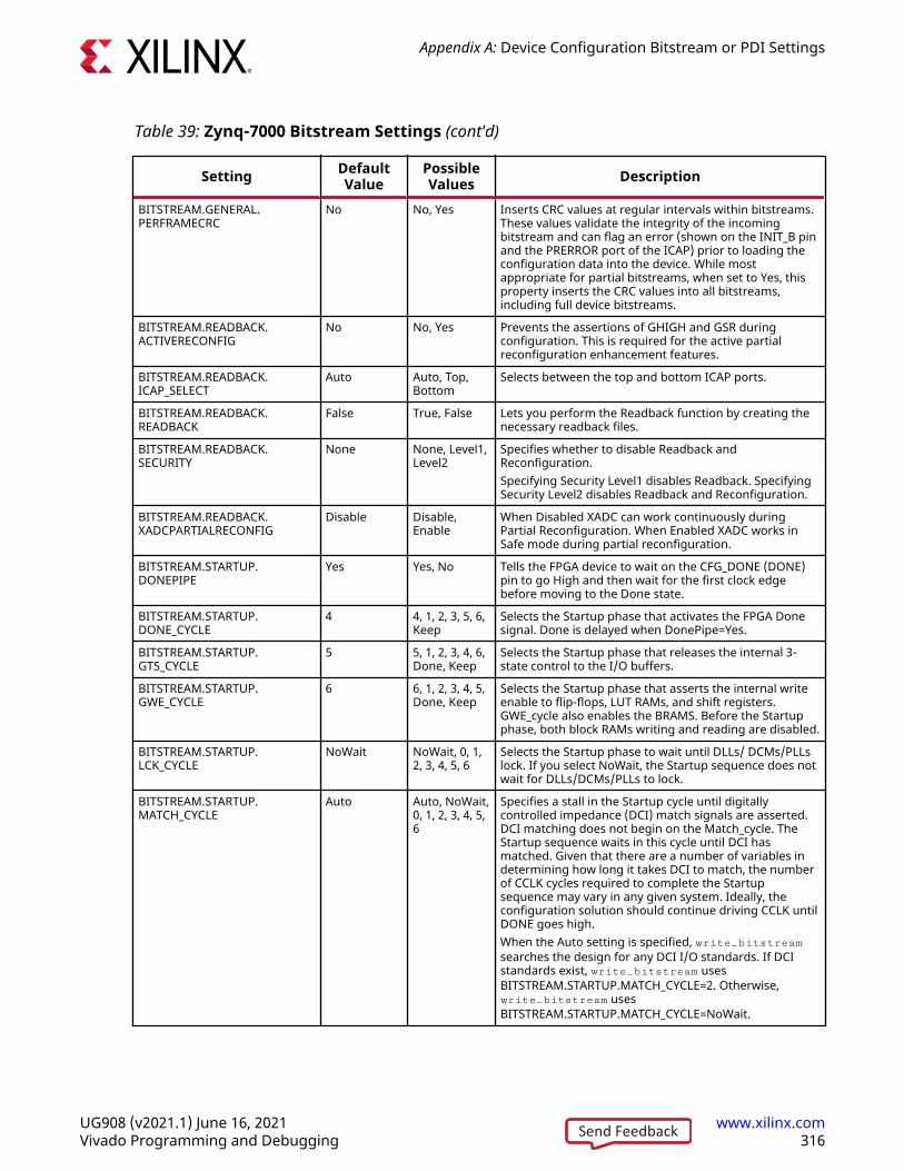
Table 39: Zynq-7000 Bitstream Settings (cont'd)
Setting DefaultValue
PossibleValues Description
BITSTREAM.GENERAL.PERFRAMECRC
No No, Yes Inserts CRC values at regular intervals within bitstreams.These values validate the integrity of the incomingbitstream and can flag an error (shown on the INIT_B pinand the PRERROR port of the ICAP) prior to loading theconfiguration data into the device. While mostappropriate for partial bitstreams, when set to Yes, thisproperty inserts the CRC values into all bitstreams,including full device bitstreams.
BITSTREAM.READBACK.ACTIVERECONFIG
No No, Yes Prevents the assertions of GHIGH and GSR duringconfiguration. This is required for the active partialreconfiguration enhancement features.
BITSTREAM.READBACK.ICAP_SELECT
Auto Auto, Top,Bottom
Selects between the top and bottom ICAP ports.
BITSTREAM.READBACK.READBACK
False True, False Lets you perform the Readback function by creating thenecessary readback files.
BITSTREAM.READBACK.SECURITY
None None, Level1,Level2
Specifies whether to disable Readback andReconfiguration.Specifying Security Level1 disables Readback. SpecifyingSecurity Level2 disables Readback and Reconfiguration.
BITSTREAM.READBACK.XADCPARTIALRECONFIG
Disable Disable,Enable
When Disabled XADC can work continuously duringPartial Reconfiguration. When Enabled XADC works inSafe mode during partial reconfiguration.
BITSTREAM.STARTUP.DONEPIPE
Yes Yes, No Tells the FPGA device to wait on the CFG_DONE (DONE)pin to go High and then wait for the first clock edgebefore moving to the Done state.
BITSTREAM.STARTUP.DONE_CYCLE
4 4, 1, 2, 3, 5, 6,Keep
Selects the Startup phase that activates the FPGA Donesignal. Done is delayed when DonePipe=Yes.
BITSTREAM.STARTUP.GTS_CYCLE
5 5, 1, 2, 3, 4, 6,Done, Keep
Selects the Startup phase that releases the internal 3-state control to the I/O buffers.
BITSTREAM.STARTUP.GWE_CYCLE
6 6, 1, 2, 3, 4, 5,Done, Keep
Selects the Startup phase that asserts the internal writeenable to flip-flops, LUT RAMs, and shift registers.GWE_cycle also enables the BRAMS. Before the Startupphase, both block RAMs writing and reading are disabled.
BITSTREAM.STARTUP.LCK_CYCLE
NoWait NoWait, 0, 1,2, 3, 4, 5, 6
Selects the Startup phase to wait until DLLs/ DCMs/PLLslock. If you select NoWait, the Startup sequence does notwait for DLLs/DCMs/PLLs to lock.
BITSTREAM.STARTUP.MATCH_CYCLE
Auto Auto, NoWait,0, 1, 2, 3, 4, 5,6
Specifies a stall in the Startup cycle until digitallycontrolled impedance (DCI) match signals are asserted.DCI matching does not begin on the Match_cycle. TheStartup sequence waits in this cycle until DCI hasmatched. Given that there are a number of variables indetermining how long it takes DCI to match, the numberof CCLK cycles required to complete the Startupsequence may vary in any given system. Ideally, theconfiguration solution should continue driving CCLK untilDONE goes high.When the Auto setting is specified, write_bitstreamsearches the design for any DCI I/O standards. If DCIstandards exist, write_bitstream usesBITSTREAM.STARTUP.MATCH_CYCLE=2. Otherwise,write_bitstream usesBITSTREAM.STARTUP.MATCH_CYCLE=NoWait.
Appendix A: Device Configuration Bitstream or PDI Settings
UG908 (v2021.1) June 16, 2021 www.xilinx.comVivado Programming and Debugging 316Send Feedback
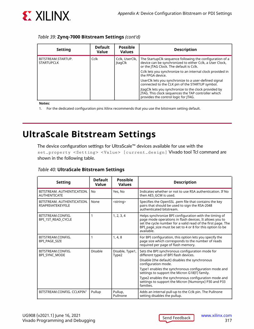
Table 39: Zynq-7000 Bitstream Settings (cont'd)
Setting DefaultValue
PossibleValues Description
BITSTREAM.STARTUP.STARTUPCLK
Cclk Cclk, UserClk,JtagClk
The StartupClk sequence following the configuration of adevice can be synchronized to either Cclk, a User Clock,or the JTAG Clock. The default is Cclk.Cclk lets you synchronize to an internal clock provided inthe FPGA device.UserClk lets you synchronize to a user-defined signalconnected to the CLK pin of the STARTUP symbol.JtagClk lets you synchronize to the clock provided byJTAG. This clock sequences the TAP controller whichprovides the control logic for JTAG.
Notes:1. For the dedicated configuration pins Xilinx recommends that you use the bitstream setting default.
UltraScale Bitstream SettingsThe device configuration settings for UltraScale™ devices available for use with theset_property <Setting> <Value> [current_design] Vivado tool Tcl command areshown in the following table.
Table 40: UltraScale Bitstream Settings
Setting DefaultValue
PossibleValues Description
BITSTREAM. AUTHENTICATION.AUTHENTICATE
No Yes, No Indicates whether or not to use RSA authentication. If Nothen AES_GCM is used.
BITSTREAM. AUTHENTICATION.RSAPRIVATEKEYFILE
None <string> Specifies the OpenSSL .pem file that contains the keypairs that should be used to sign the RSA-2048authenticated bitstream.
BITSTREAM.CONFIG.BPI_1ST_READ_CYCLE
1 1, 2, 3, 4 Helps synchronize BPI configuration with the timing ofpage mode operations in flash devices. It allows you toset the cycle number for a valid read of the first page. TheBPI_page_size must be set to 4 or 8 for this option to beavailable.
BITSTREAM.CONFIG.BPI_PAGE_SIZE
1 1, 4, 8 For BPI configuration, this option lets you specify thepage size which corresponds to the number of readsrequired per page of flash memory.
BITSTREAM.CONFIG.BPI_SYNC_MODE
Disable Disable, Type1,Type2
Sets the BPI synchronous configuration mode fordifferent types of BPI flash devices.Disable (the default) disables the synchronousconfiguration mode.Type1 enables the synchronous configuration mode andsettings to support the Micron G18(F) family.Type2 enables the synchronous configuration mode andsettings to support the Micron (Numonyx) P30 and P33families.
BITSTREAM.CONFIG. CCLKPIN1 Pullup Pullup,Pullnone
Adds an internal pull-up to the Cclk pin. The Pullnonesetting disables the pullup.
Appendix A: Device Configuration Bitstream or PDI Settings
UG908 (v2021.1) June 16, 2021 www.xilinx.comVivado Programming and Debugging 317Send Feedback
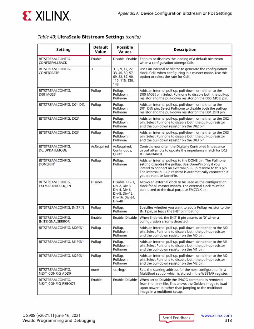
Table 40: UltraScale Bitstream Settings (cont'd)
Setting DefaultValue
PossibleValues Description
BITSTREAM.CONFIG.CONFIGFALLBACK
Enable Disable, Enable Enables or disables the loading of a default bitstreamwhen a configuration attempt fails.
BITSTREAM.CONFIG.CONFIGRATE
3 3, 6, 9, 12, 22,33, 40, 50, 57,69, 82, 87, 90,110, 115, 130,148
Uses an internal oscillator to generate the configurationclock, Cclk, when configuring in a master mode. Use thisoption to select the rate for Cclk.
BITSTREAM.CONFIG.D00_MOSI1
Pullup Pullup,Pulldown,Pullnone
Adds an internal pull-up, pull-down, or neither to theD00_MOSI pin. Select Pullnone to disable both the pull-upresistor and the pull-down resistor on the D00_MOSI pin.
BITSTREAM.CONFIG. D01_DIN1 Pullup Pullup,Pulldown,Pullnone
Adds an internal pull-up, pull-down, or neither to theD01_DIN pin. Select Pullnone to disable both the pull-upresistor and the pull-down resistor on the D01_DIN pin.
BITSTREAM.CONFIG. D021 Pullup Pullup,Pulldown,Pullnone
Adds an internal pull-up, pull-down, or neither to the D02pin. Select Pullnone to disable both the pull-up resistorand the pull-down resistor on the D02 pin.
BITSTREAM.CONFIG. D031 Pullup Pullup,Pulldown,Pullnone
Adds an internal pull-up, pull-down, or neither to the D03pin. Select Pullnone to disable both the pull-up resistorand the pull-down resistor on the D03 pin.
BITSTREAM.CONFIG.DCIUPDATEMODE
AsRequired AsRequired,Continuous,Quiet
Controls how often the Digitally Controlled Impedancecircuit attempts to update the impedance match for DCIIOSTANDARDs.
BITSTREAM.CONFIG.DONEPIN1
Pullup Pullup,Pullnone
Adds an internal pull-up to the DONE pin. The Pullnonesetting disables the pullup. Use DonePin only if youintend to connect an external pull-up resistor to this pin.The internal pull-up resistor is automatically connected ifyou do not use DonePin.
BITSTREAM.CONFIG.EXTMASTERCCLK_EN
Disable Disable, Div-1,Div-2, Div-3,Div-4, Div-6,Div-8, Div-12,Div-16, Div-24,Div-48
Allows an external clock to be used as the configurationclock for all master modes. The external clock must beconnected to the dual-purpose EMCCLK pin.
BITSTREAM.CONFIG. INITPIN1 Pullup Pullup,Pullnone
Specifies whether you want to add a Pullup resistor to theINIT pin, or leave the INIT pin floating.
BITSTREAM.CONFIG.INITSIGNALSERROR
Enable Enable, Disable When Enabled, the INIT_B pin asserts to '0' when aconfiguration error is detected.
BITSTREAM.CONFIG. M0PIN1 Pullup Pullup,Pulldown,Pullnone
Adds an internal pull-up, pull-down, or neither to the M0pin. Select Pullnone to disable both the pull-up resistorand the pull-down resistor on the M0 pin.
BITSTREAM.CONFIG. M1PIN1 Pullup Pullup,Pulldown,Pullnone
Adds an internal pull-up, pull-down, or neither to the M1pin. Select Pullnone to disable both the pull-up resistorand the pull-down resistor on the M1 pin.
BITSTREAM.CONFIG. M2PIN1 Pullup Pullup,Pulldown,Pullnone
Adds an internal pull-up, pull-down, or neither to the M2pin. Select Pullnone to disable both the pull-up resistorand the pull-down resistor on the M2 pin.
BITSTREAM.CONFIG.NEXT_CONFIG_ADDR
none <string> Sets the starting address for the next configuration in aMultiBoot set up, which is stored in the WBSTAR register.
BITSTREAM.CONFIG.NEXT_CONFIG_REBOOT
Enable Enable, Disable When set to Disable the IPROG command is removedfrom the .bit file. This allows the Golden image to loadupon power up rather than jumping to the multibootimage in a multiboot setup.
Appendix A: Device Configuration Bitstream or PDI Settings
UG908 (v2021.1) June 16, 2021 www.xilinx.comVivado Programming and Debugging 318Send Feedback
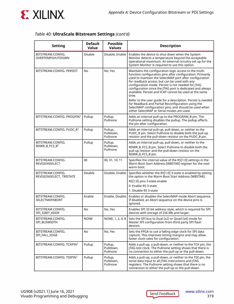
Table 40: UltraScale Bitstream Settings (cont'd)
Setting DefaultValue
PossibleValues Description
BITSTREAM.CONFIG.OVERTEMPSHUTDOWN
Disable Disable, Enable Enables the device to shut down when the SystemMonitor detects a temperature beyond the acceptableoperational maximum. An external circuitry set up for theSystem Monitor is required to use this option.
BITSTREAM.CONFIG. PERSIST No No, Yes Maintains the configuration logic access to the multi-function configuration pins after configuration. Primarilyused to maintain the SelectMAP port after configurationfor readback access, but can be used with anyconfiguration mode. Persist is not needed for JTAGconfiguration since the JTAG port is dedicated and alwaysavailable. Persist and ICAP cannot be used at the sametime.Refer to the user guide for a description. Persist is neededfor Readback and Partial Reconfiguration using theSelectMAP configuration pins, and should be used wheneither SelectMAP or Serial modes are used.
BITSTREAM.CONFIG. PROGPIN1 Pullup Pullup,Pullnone
Adds an internal pull-up to the PROGRAM_B pin. ThePullnone setting disables the pullup. The pullup affectsthe pin after configuration.
BITSTREAM.CONFIG. PUDC_B1 Pullup Pullup,Pulldown,Pullnone
Adds an internal pull-up, pull-down, or neither to thePUDC_B pin. Select Pullnone to disable both the pull-upresistor and the pull-down resistor on the PUDC_B pin.
BITSTREAM.CONFIG.RDWR_B_FCS_B1
Pullup Pullup,Pulldown,Pullnone
Adds an internal pull-up, pull-down, or neither to theRDWR_B_FCS_B pin. Select Pullnone to disable both thepull-up resistor and the pull-down resistor on theRDWR_B_FCS_B pin.
BITSTREAM.CONFIG.REVISIONSELECT
00 00, 01, 10, 11 Specifies the internal value of the RS[1:0] settings in theWarm Boot Start Address (WBSTAR) register for the nextwarm boot.
BITSTREAM.CONFIG.REVISIONSELECT_ TRISTATE
Disable Disable, Enable Specifies whether the RS[1:0] 3-state is enabled by settingthe option in the Warm Boot Start Address (WBSTAR).RS[1:0] pins 3-state enable0: Enable RS 3-state1: Disable RS 3-state
BITSTREAM.CONFIG.SELECTMAPABORT
Enable Enable, Disable Enables or disables the SelectMAP mode Abort sequence.If disabled, an Abort sequence on the device pins isignored.
BITSTREAM.CONFIG.SPI_32BIT_ADDR
No No, Yes Enables SPI 32-bit address style, which is required for SPIdevices with storage of 256 Mb and larger.
BITSTREAM.CONFIG.SPI_BUSWIDTH
NONE NONE, 1, 2, 4, 8 Sets the SPI bus to Dual (x2) or Quad (x4) mode forMaster SPI configuration from third party SPI flashdevices.
BITSTREAM.CONFIG.SPI_FALL_EDGE
No No, Yes Sets the FPGA to use a falling edge clock for SPI datacapture. This improves timing margins and may allowfaster clock rates for configuration.
BITSTREAM.CONFIG. TCKPIN1 Pullup Pullup,Pulldown,Pullnone
Adds a pull-up, a pull-down, or neither to the TCK pin, theJTAG test clock. The Pullnone setting shows that there isno connection to either the pull-up or the pull-down.
BITSTREAM.CONFIG. TDIPIN1 Pullup Pullup,Pulldown,Pullnone
Adds a pull-up, a pull-down, or neither to the TDI pin, theserial data input to all JTAG instructions and JTAGregisters. The Pullnone setting shows that there is noconnection to either the pull-up or the pull-down.
Appendix A: Device Configuration Bitstream or PDI Settings
UG908 (v2021.1) June 16, 2021 www.xilinx.comVivado Programming and Debugging 319Send Feedback
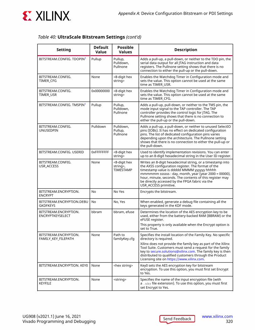
Table 40: UltraScale Bitstream Settings (cont'd)
Setting DefaultValue
PossibleValues Description
BITSTREAM.CONFIG. TDOPIN1 Pullup Pullup,Pulldown,Pullnone
Adds a pull-up, a pull-down, or neither to the TDO pin, theserial data output for all JTAG instruction and dataregisters. The Pullnone setting shows that there is noconnection to either the pull-up or the pull-down.
BITSTREAM.CONFIG.TIMER_CFG
None <8-digit hexstring>
Enables the Watchdog Timer in Configuration mode andsets the value. This option cannot be used at the sametime as TIMER_USR.
BITSTREAM.CONFIG.TIMER_USR
0x00000000 <8-digit hexstring>
Enables the Watchdog Timer in Configuration mode andsets the value. This option cannot be used at the sametime as TIMER_CFG.
BITSTREAM.CONFIG. TMSPIN1 Pullup Pullup,Pulldown,Pullnone
Adds a pull-up, pull-down, or neither to the TMS pin, themode input signal to the TAP controller. The TAPcontroller provides the control logic for JTAG. ThePullnone setting shows that there is no connection toeither the pull-up or the pull-down.
BITSTREAM.CONFIG.UNUSEDPIN
Pulldown Pulldown,Pullup,Pullnone
Adds a pull-up, a pull-down, or neither to unused SelectIOpins (IOBs). It has no effect on dedicated configurationpins. The list of dedicated configuration pins variesdepending upon the architecture. The Pullnone settingshows that there is no connection to either the pull-up orthe pull-down.
BITSTREAM.CONFIG. USERID 0xFFFFFFFF <8-digit hexstring>
Used to identify implementation revisions. You can enterup to an 8-digit hexadecimal string in the User ID register.
BITSTREAM.CONFIG.USR_ACCESS
None <8-digit hexstring>,TIMESTAMP
Writes an 8-digit hexadecimal string, or a timestamp intothe AXSS configuration register. The format of thetimestamp value is ddddd MMMM yyyyyy hhhhhmmmmmm ssssss : day, month, year (year 2000 = 00000),hour, minute, seconds. The contents of this register maybe directly accessed by the FPGA fabric via theUSR_ACCESS primitive.
BITSTREAM.ENCRYPTION.ENCRYPT
No No Yes Encrypts the bitstream.
BITSTREAM.ENCRYPTION.DEBUGKDFKEYS
No No, Yes When enabled, generate a debug file containing all thekeys generated in the KDF mode.
BITSTREAM.ENCRYPTION.ENCRYPTKEYSELECT
bbram bbram, efuse Determines the location of the AES encryption key to beused, either from the battery-backed RAM (BBRAM) or theeFUSE register.This property is only available when the Encrypt option isset to True.
BITSTREAM.ENCRYPTION.FAMILY_KEY_FILEPATH
None Path tofamilyKey.cfg
Specifies the install location of the Family Key. No specificdirectory is required.Xilinx does not provide the family key as part of the XilinxTool Suite. Customers must send a request for the familykey to [email protected]. The family key is thendistributed to qualified customers through the ProductLicensing site on https://www.xilinx.com.
BITSTREAM.ENCRYPTION. KEY0 None <hex string> Key0 sets the AES encryption key for bitstreamencryption. To use this option, you must first set Encryptto Yes.
BITSTREAM.ENCRYPTION.KEYFILE
None <string> Specifies the name of the input encryption file (witha .nky file extension). To use this option, you must firstset Encrypt to Yes.
Appendix A: Device Configuration Bitstream or PDI Settings
UG908 (v2021.1) June 16, 2021 www.xilinx.comVivado Programming and Debugging 320Send Feedback
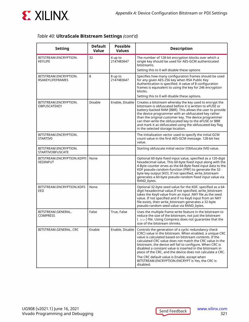
Table 40: UltraScale Bitstream Settings (cont'd)
Setting DefaultValue
PossibleValues Description
BITSTREAM.ENCRYPTION.KEYLIFE
32 4 up to2147483647
The number of 128-bit encryption blocks over which asingle key should be used for AES-GCM authenticatedbitstreams.Setting this to 0 will disable these options
BITSTREAM.ENCRYPTION.RSAKEYLIFEFRAMES
8 8 up to2147483647
Specifies how many configuration frames should be usedfor any given AES-256 key when RSA Public KeyAuthentication is specified. A value of 8 configurationframes is equivalent to using the key for 246 encryptionblocks.Setting this to 0 will disable these options.
BITSTREAM.ENCRYPTION.OBFUSCATEKEY
Disable Enable, Disable Creates a bitstream whereby the key used to encrypt thebitstream is obfuscated before it is written to eFUSE orbattery-backed RAM (BBR). This allows the user to providethe device programmer with an obfuscated key ratherthan the original customer key. The device programmercan then write the obfuscated key to the eFUSE or BBRand mark it as obfuscated using the obfuscated-key flagin the selected storage location.
BITSTREAM.ENCRYPTION.STARTIV0
The initialization vector used to specify the initial GCMcount value in the first AES-GCM message. 128-bit hexvalue.
BITSTREAM.ENCRYPTION.STARTIVOBFUSCATE
Starting obfuscate initial vector (Obfuscate IV0) value.
BITSTREAM.ENCRYPTION.KDFFIXEDINPUT
None Optional 60-byte fixed input value, specified as a 120-digithexadecimal value. This 60-byte fixed input along with the4-Byte counter erves as the 64-Byte fixed input data to theKDF pseudo-random-function (PRF) to generate the 32-byte key output (KO). If not specified, write_bitstreamgenerates a 60-byte pseudo-random fixed input value viaRAND_bytes.
BITSTREAM.ENCRYPTION.KDFSEED
None Optional 32-byte seed value for the KDF, specified as a 64-digit hexadecimal value.If not specified, write_bitstreamtakes the Key0 value from an input .NKY file as the seedvalue. If not specified and if no Key0 input from an NKYfile exists, then write_bitstream generates a 32-bytepseudo-random seed value via RAND_bytes.
BITSTREAM.GENERAL.COMPRESS
False True, False Uses the multiple frame write feature in the bitstream toreduce the size of the bitstream, not just the bitstream(.bit) file. Using Compress does not guarantee that thesize of the bitstream shrinks.
BITSTREAM.GENERAL. CRC Enable Enable, Disable Controls the generation of a cyclic redundancy check(CRC) value in the bitstream. When enabled, a unique CRCvalue is calculated based on bitstream contents. If thecalculated CRC value does not match the CRC value in thebitstream, the device will fail to configure. When CRC isdisabled a constant value is inserted in the bitstream inplace of the CRC, and the device does not calculate a CRC.The CRC default value is Enable, except whenBITSTREAM.ENCRYPTION.ENCRYPT is Yes, the CRC isdisabled.
Appendix A: Device Configuration Bitstream or PDI Settings
UG908 (v2021.1) June 16, 2021 www.xilinx.comVivado Programming and Debugging 321Send Feedback
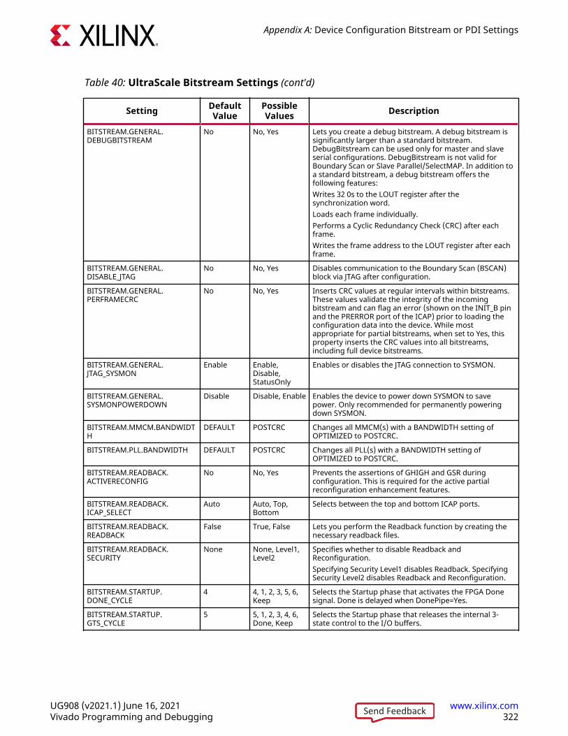
Table 40: UltraScale Bitstream Settings (cont'd)
Setting DefaultValue
PossibleValues Description
BITSTREAM.GENERAL.DEBUGBITSTREAM
No No, Yes Lets you create a debug bitstream. A debug bitstream issignificantly larger than a standard bitstream.DebugBitstream can be used only for master and slaveserial configurations. DebugBitstream is not valid forBoundary Scan or Slave Parallel/SelectMAP. In addition toa standard bitstream, a debug bitstream offers thefollowing features:Writes 32 0s to the LOUT register after thesynchronization word.Loads each frame individually.Performs a Cyclic Redundancy Check (CRC) after eachframe.Writes the frame address to the LOUT register after eachframe.
BITSTREAM.GENERAL.DISABLE_JTAG
No No, Yes Disables communication to the Boundary Scan (BSCAN)block via JTAG after configuration.
BITSTREAM.GENERAL.PERFRAMECRC
No No, Yes Inserts CRC values at regular intervals within bitstreams.These values validate the integrity of the incomingbitstream and can flag an error (shown on the INIT_B pinand the PRERROR port of the ICAP) prior to loading theconfiguration data into the device. While mostappropriate for partial bitstreams, when set to Yes, thisproperty inserts the CRC values into all bitstreams,including full device bitstreams.
BITSTREAM.GENERAL.JTAG_SYSMON
Enable Enable,Disable,StatusOnly
Enables or disables the JTAG connection to SYSMON.
BITSTREAM.GENERAL.SYSMONPOWERDOWN
Disable Disable, Enable Enables the device to power down SYSMON to savepower. Only recommended for permanently poweringdown SYSMON.
BITSTREAM.MMCM.BANDWIDTH
DEFAULT POSTCRC Changes all MMCM(s) with a BANDWIDTH setting ofOPTIMIZED to POSTCRC.
BITSTREAM.PLL.BANDWIDTH DEFAULT POSTCRC Changes all PLL(s) with a BANDWIDTH setting ofOPTIMIZED to POSTCRC.
BITSTREAM.READBACK.ACTIVERECONFIG
No No, Yes Prevents the assertions of GHIGH and GSR duringconfiguration. This is required for the active partialreconfiguration enhancement features.
BITSTREAM.READBACK.ICAP_SELECT
Auto Auto, Top,Bottom
Selects between the top and bottom ICAP ports.
BITSTREAM.READBACK.READBACK
False True, False Lets you perform the Readback function by creating thenecessary readback files.
BITSTREAM.READBACK.SECURITY
None None, Level1,Level2
Specifies whether to disable Readback andReconfiguration.Specifying Security Level1 disables Readback. SpecifyingSecurity Level2 disables Readback and Reconfiguration.
BITSTREAM.STARTUP.DONE_CYCLE
4 4, 1, 2, 3, 5, 6,Keep
Selects the Startup phase that activates the FPGA Donesignal. Done is delayed when DonePipe=Yes.
BITSTREAM.STARTUP.GTS_CYCLE
5 5, 1, 2, 3, 4, 6,Done, Keep
Selects the Startup phase that releases the internal 3-state control to the I/O buffers.
Appendix A: Device Configuration Bitstream or PDI Settings
UG908 (v2021.1) June 16, 2021 www.xilinx.comVivado Programming and Debugging 322Send Feedback

Table 40: UltraScale Bitstream Settings (cont'd)
Setting DefaultValue
PossibleValues Description
BITSTREAM.STARTUP.GWE_CYCLE
6 6, 1, 2, 3, 4, 5,Done, Keep
Selects the Startup phase that asserts the internal writeenable to flip-flops, LUT RAMs, and shift registers.GWE_cycle also enables the BRAMS. Before the Startupphase, both block RAMs writing and reading are disabled.
BITSTREAM.STARTUP.LCK_CYCLE
NoWait NoWait, 0, 1, 2,3, 4, 5, 6
Selects the Startup phase to wait until DLLs/DCMs/PLLslock. If you select NoWait, the Startup sequence does notwait for DLLs/DCMs/PLLs to lock.
BITSTREAM.STARTUP.MATCH_CYCLE
Auto Auto, NoWait,0, 1, 2, 3, 4, 5, 6
Specifies a stall in the Startup cycle until digitallycontrolled impedance (DCI) match signals are asserted.DCI matching does not begin on the Match_cycle. TheStartup sequence waits in this cycle until DCI hasmatched. Given that there are a number of variables indetermining how long it takes DCI to match, the numberof CCLK cycles required to complete the Startup sequencemay vary in any given system. Ideally, the configurationsolution should continue driving CCLK until DONE goesHigh.When the Auto setting is specified, write_bitstreamsearches the design for any DCI I/O standards. If DCIstandards exist, write_bitstream usesBITSTREAM.STARTUP.MATCH_CYCLE=2. Otherwise,write_bitstream usesBITSTREAM.STARTUP.MATCH_CYCLE=NoWait.
Notes:1. For the dedicated configuration pins Xilinx recommends that you use the default bitstream setting.
Virtex and Kintex UltraScale+ BitstreamSettings
The device configuration settings for the Virtex® UltraScale™ and Kintex® UltraScale+™ devicesavailable for use with the set_property <Setting> <Value> [current_design]Vivado® tool Tcl command are shown in the following table.
Table 41: Virtex UltraScale and Kintex UltraScale+ Bitstream Settings
Setting DefaultValues
PossibleValues Description
BITSTREAM. AUTHENTICATION.AUTHENTICATE
No No, Yes Indicates whether or not to use RSA authentication. If Nothen AES_GCM is used.
BITSTREAM. AUTHENTICATION.RSAPRIVATEKEYFILE
Specifies the OpenSSL .pem file that contains the keypairs that should be used to sign the RSA-2048authenticated bitstream.
BITSTREAM.CONFIG.BPI_1ST_READ_CYCLE
1 1, 2, 3, 4 Helps synchronize BPI configuration with the timing ofpage mode operations in flash devices. It allows you toset the cycle number for a valid read of the first page.The BPI_page_size must be set to 4 or 8 for this option tobe available.
Appendix A: Device Configuration Bitstream or PDI Settings
UG908 (v2021.1) June 16, 2021 www.xilinx.comVivado Programming and Debugging 323Send Feedback
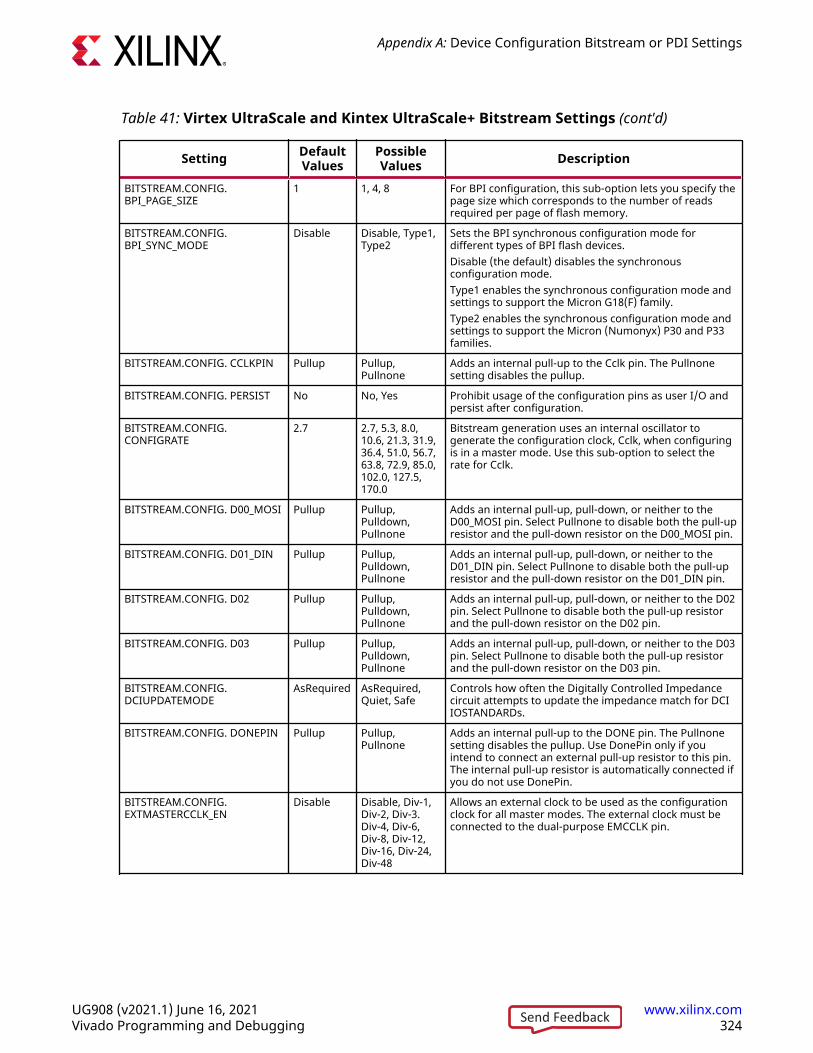
Table 41: Virtex UltraScale and Kintex UltraScale+ Bitstream Settings (cont'd)
Setting DefaultValues
PossibleValues Description
BITSTREAM.CONFIG.BPI_PAGE_SIZE
1 1, 4, 8 For BPI configuration, this sub-option lets you specify thepage size which corresponds to the number of readsrequired per page of flash memory.
BITSTREAM.CONFIG.BPI_SYNC_MODE
Disable Disable, Type1,Type2
Sets the BPI synchronous configuration mode fordifferent types of BPI flash devices.Disable (the default) disables the synchronousconfiguration mode.Type1 enables the synchronous configuration mode andsettings to support the Micron G18(F) family.Type2 enables the synchronous configuration mode andsettings to support the Micron (Numonyx) P30 and P33families.
BITSTREAM.CONFIG. CCLKPIN Pullup Pullup,Pullnone
Adds an internal pull-up to the Cclk pin. The Pullnonesetting disables the pullup.
BITSTREAM.CONFIG. PERSIST No No, Yes Prohibit usage of the configuration pins as user I/O andpersist after configuration.
BITSTREAM.CONFIG.CONFIGRATE
2.7 2.7, 5.3, 8.0,10.6, 21.3, 31.9,36.4, 51.0, 56.7,63.8, 72.9, 85.0,102.0, 127.5,170.0
Bitstream generation uses an internal oscillator togenerate the configuration clock, Cclk, when configuringis in a master mode. Use this sub-option to select therate for Cclk.
BITSTREAM.CONFIG. D00_MOSI Pullup Pullup,Pulldown,Pullnone
Adds an internal pull-up, pull-down, or neither to theD00_MOSI pin. Select Pullnone to disable both the pull-upresistor and the pull-down resistor on the D00_MOSI pin.
BITSTREAM.CONFIG. D01_DIN Pullup Pullup,Pulldown,Pullnone
Adds an internal pull-up, pull-down, or neither to theD01_DIN pin. Select Pullnone to disable both the pull-upresistor and the pull-down resistor on the D01_DIN pin.
BITSTREAM.CONFIG. D02 Pullup Pullup,Pulldown,Pullnone
Adds an internal pull-up, pull-down, or neither to the D02pin. Select Pullnone to disable both the pull-up resistorand the pull-down resistor on the D02 pin.
BITSTREAM.CONFIG. D03 Pullup Pullup,Pulldown,Pullnone
Adds an internal pull-up, pull-down, or neither to the D03pin. Select Pullnone to disable both the pull-up resistorand the pull-down resistor on the D03 pin.
BITSTREAM.CONFIG.DCIUPDATEMODE
AsRequired AsRequired,Quiet, Safe
Controls how often the Digitally Controlled Impedancecircuit attempts to update the impedance match for DCIIOSTANDARDs.
BITSTREAM.CONFIG. DONEPIN Pullup Pullup,Pullnone
Adds an internal pull-up to the DONE pin. The Pullnonesetting disables the pullup. Use DonePin only if youintend to connect an external pull-up resistor to this pin.The internal pull-up resistor is automatically connected ifyou do not use DonePin.
BITSTREAM.CONFIG.EXTMASTERCCLK_EN
Disable Disable, Div-1,Div-2, Div-3.Div-4, Div-6,Div-8, Div-12,Div-16, Div-24,Div-48
Allows an external clock to be used as the configurationclock for all master modes. The external clock must beconnected to the dual-purpose EMCCLK pin.
Appendix A: Device Configuration Bitstream or PDI Settings
UG908 (v2021.1) June 16, 2021 www.xilinx.comVivado Programming and Debugging 324Send Feedback
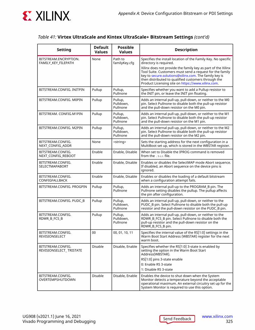
Table 41: Virtex UltraScale and Kintex UltraScale+ Bitstream Settings (cont'd)
Setting DefaultValues
PossibleValues Description
BITSTREAM.ENCRYPTION.FAMILY_KEY_FILEPATH
None Path tofamilyKey.cfg
Specifies the install location of the Family Key. No specificdirectory is required.Xilinx does not provide the family key as part of the XilinxTool Suite. Customers must send a request for the familykey to [email protected]. The family key isthen distributed to qualified customers through theProduct Licensing site on https://www.xilinx.com.
BITSTREAM.CONFIG. INITPIN Pullup Pullup,Pullnone
Specifies whether you want to add a Pullup resistor tothe INIT pin, or leave the INIT pin floating.
BITSTREAM.CONFIG. M0PIN Pullup Pullup,Pulldown,Pullnone
Adds an internal pull-up, pull-down, or neither to the M0pin. Select Pullnone to disable both the pull-up resistorand the pull-down resistor on the M0 pin.
BITSTREAM. CONFIG.M1PIN Pullup Pullup,Pulldown,Pullnone
Adds an internal pull-up, pull-down, or neither to the M1pin. Select Pullnone to disable both the pull-up resistorand the pull-down resistor on the M1 pin.
BITSTREAM.CONFIG. M2PIN Pullup Pullup,Pulldown,Pullnone
Adds an internal pull-up, pull-down, or neither to the M2pin. Select Pullnone to disable both the pull-up resistorand the pull-down resistor on the M2 pin.
BITSTREAM.CONFIG.NEXT_CONFIG_ADDR
None <string> Sets the starting address for the next configuration in aMultiBoot set up, which is stored in the WBSTAR register.
BITSTREAM.CONFIG.NEXT_CONFIG_REBOOT
Enable Enable, Disable When set to Disable the IPROG command is removedfrom the .bit file.
BITSTREAM.CONFIG.SELECTMAPABORT
Enable Enable, Disable Enables or disables the SelectMAP mode Abort sequence.If disabled, an Abort sequence on the device pins isignored.
BITSTREAM.CONFIG.CONFIGFALLBACK
Enable Enable, Disable Enables or disables the loading of a default bitstreamwhen a configuration attempt fails.
BITSTREAM.CONFIG. PROGPIN Pullup Pullup,Pullnone
Adds an internal pull-up to the PROGRAM_B pin. ThePullnone setting disables the pullup. The pullup affectsthe pin after configuration.
BITSTREAM.CONFIG. PUDC_B Pullup Pullup,Pulldown,Pullnone
Adds an internal pull-up, pull-down, or neither to thePUDC_B pin. Select Pullnone to disable both the pull-upresistor and the pull-down resistor on the PUDC_B pin.
BITSTREAM.CONFIG.RDWR_B_FCS_B
Pullup Pullup,Pulldown,Pullnone
Adds an internal pull-up, pull-down, or neither to theRDWR_B_FCS_B pin. Select Pullnone to disable both thepull-up resistor and the pull-down resistor on theRDWR_B_FCS_B pin.
BITSTREAM.CONFIG.REVISIONSELECT
00 00, 01, 10, 11 Specifies the internal value of the RS[1:0] settings in theWarm Boot Start Address (WBSTAR) register for the nextwarm boot.
BITSTREAM.CONFIG.REVISIONSELECT_ TRISTATE
Disable Disable, Enable Specifies whether the RS[1:0] 3-state is enabled bysetting the option in the Warm Boot StartAddress(WBSTAR).RS[1:0] pins 3-state enable0: Enable RS 3-state1: Disable RS 3-state
BITSTREAM.CONFIG.OVERTEMPSHUTDOWN
Disable Disable, Enable Enables the device to shut down when the SystemMonitor detects a temperature beyond the acceptableoperational maximum. An external circuitry set up for theSystem Monitor is required to use this option.
Appendix A: Device Configuration Bitstream or PDI Settings
UG908 (v2021.1) June 16, 2021 www.xilinx.comVivado Programming and Debugging 325Send Feedback
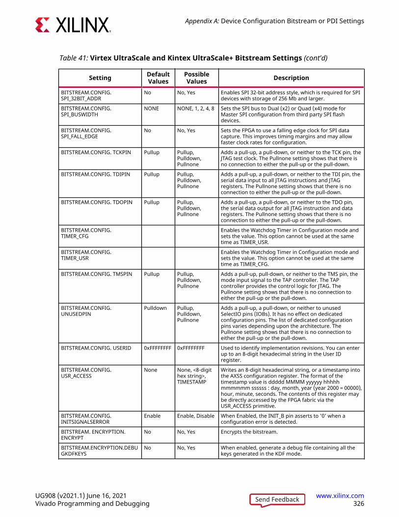
Table 41: Virtex UltraScale and Kintex UltraScale+ Bitstream Settings (cont'd)
Setting DefaultValues
PossibleValues Description
BITSTREAM.CONFIG.SPI_32BIT_ADDR
No No, Yes Enables SPI 32-bit address style, which is required for SPIdevices with storage of 256 Mb and larger.
BITSTREAM.CONFIG.SPI_BUSWIDTH
NONE NONE, 1, 2, 4, 8 Sets the SPI bus to Dual (x2) or Quad (x4) mode forMaster SPI configuration from third party SPI flashdevices.
BITSTREAM.CONFIG.SPI_FALL_EDGE
No No, Yes Sets the FPGA to use a falling edge clock for SPI datacapture. This improves timing margins and may allowfaster clock rates for configuration.
BITSTREAM.CONFIG. TCKPIN Pullup Pullup,Pulldown,Pullnone
Adds a pull-up, a pull-down, or neither to the TCK pin, theJTAG test clock. The Pullnone setting shows that there isno connection to either the pull-up or the pull-down.
BITSTREAM.CONFIG. TDIPIN Pullup Pullup,Pulldown,Pullnone
Adds a pull-up, a pull-down, or neither to the TDI pin, theserial data input to all JTAG instructions and JTAGregisters. The Pullnone setting shows that there is noconnection to either the pull-up or the pull-down.
BITSTREAM.CONFIG. TDOPIN Pullup Pullup,Pulldown,Pullnone
Adds a pull-up, a pull-down, or neither to the TDO pin,the serial data output for all JTAG instruction and dataregisters. The Pullnone setting shows that there is noconnection to either the pull-up or the pull-down.
BITSTREAM.CONFIG.TIMER_CFG
Enables the Watchdog Timer in Configuration mode andsets the value. This option cannot be used at the sametime as TIMER_USR.
BITSTREAM.CONFIG.TIMER_USR
Enables the Watchdog Timer in Configuration mode andsets the value. This option cannot be used at the sametime as TIMER_CFG.
BITSTREAM.CONFIG. TMSPIN Pullup Pullup,Pulldown,Pullnone
Adds a pull-up, pull-down, or neither to the TMS pin, themode input signal to the TAP controller. The TAPcontroller provides the control logic for JTAG. ThePullnone setting shows that there is no connection toeither the pull-up or the pull-down.
BITSTREAM.CONFIG.UNUSEDPIN
Pulldown Pullup,Pulldown,Pullnone
Adds a pull-up, a pull-down, or neither to unusedSelectIO pins (IOBs). It has no effect on dedicatedconfiguration pins. The list of dedicated configurationpins varies depending upon the architecture. ThePullnone setting shows that there is no connection toeither the pull-up or the pull-down.
BITSTREAM.CONFIG. USERID 0xFFFFFFFF 0xFFFFFFFF Used to identify implementation revisions. You can enterup to an 8-digit hexadecimal string in the User IDregister.
BITSTREAM.CONFIG.USR_ACCESS
None None, <8-digithex string>,TIMESTAMP
Writes an 8-digit hexadecimal string, or a timestamp intothe AXSS configuration register. The format of thetimestamp value is ddddd MMMM yyyyyy hhhhhmmmmmm ssssss : day, month, year (year 2000 = 00000),hour, minute, seconds. The contents of this register maybe directly accessed by the FPGA fabric via theUSR_ACCESS primitive.
BITSTREAM.CONFIG.INITSIGNALSERROR
Enable Enable, Disable When Enabled, the INIT_B pin asserts to '0' when aconfiguration error is detected.
BITSTREAM. ENCRYPTION.ENCRYPT
No No, Yes Encrypts the bitstream.
BITSTREAM.ENCRYPTION.DEBUGKDFKEYS
No No, Yes When enabled, generate a debug file containing all thekeys generated in the KDF mode.
Appendix A: Device Configuration Bitstream or PDI Settings
UG908 (v2021.1) June 16, 2021 www.xilinx.comVivado Programming and Debugging 326Send Feedback
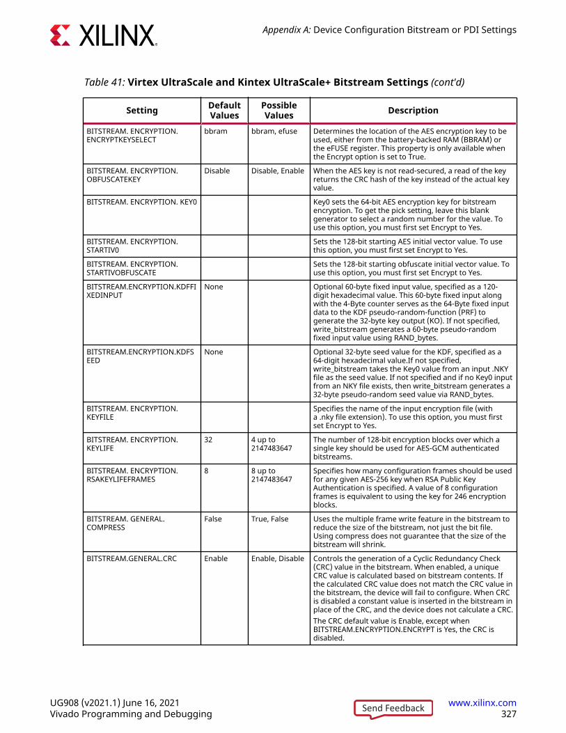
Table 41: Virtex UltraScale and Kintex UltraScale+ Bitstream Settings (cont'd)
Setting DefaultValues
PossibleValues Description
BITSTREAM. ENCRYPTION.ENCRYPTKEYSELECT
bbram bbram, efuse Determines the location of the AES encryption key to beused, either from the battery-backed RAM (BBRAM) orthe eFUSE register. This property is only available whenthe Encrypt option is set to True.
BITSTREAM. ENCRYPTION.OBFUSCATEKEY
Disable Disable, Enable When the AES key is not read-secured, a read of the keyreturns the CRC hash of the key instead of the actual keyvalue.
BITSTREAM. ENCRYPTION. KEY0 Key0 sets the 64-bit AES encryption key for bitstreamencryption. To get the pick setting, leave this blankgenerator to select a random number for the value. Touse this option, you must first set Encrypt to Yes.
BITSTREAM. ENCRYPTION.STARTIV0
Sets the 128-bit starting AES initial vector value. To usethis option, you must first set Encrypt to Yes.
BITSTREAM. ENCRYPTION.STARTIVOBFUSCATE
Sets the 128-bit starting obfuscate initial vector value. Touse this option, you must first set Encrypt to Yes.
BITSTREAM.ENCRYPTION.KDFFIXEDINPUT
None Optional 60-byte fixed input value, specified as a 120-digit hexadecimal value. This 60-byte fixed input alongwith the 4-Byte counter serves as the 64-Byte fixed inputdata to the KDF pseudo-random-function (PRF) togenerate the 32-byte key output (KO). If not specified,write_bitstream generates a 60-byte pseudo-randomfixed input value using RAND_bytes.
BITSTREAM.ENCRYPTION.KDFSEED
None Optional 32-byte seed value for the KDF, specified as a64-digit hexadecimal value.If not specified,write_bitstream takes the Key0 value from an input .NKYfile as the seed value. If not specified and if no Key0 inputfrom an NKY file exists, then write_bitstream generates a32-byte pseudo-random seed value via RAND_bytes.
BITSTREAM. ENCRYPTION.KEYFILE
Specifies the name of the input encryption file (witha .nky file extension). To use this option, you must firstset Encrypt to Yes.
BITSTREAM. ENCRYPTION.KEYLIFE
32 4 up to2147483647
The number of 128-bit encryption blocks over which asingle key should be used for AES-GCM authenticatedbitstreams.
BITSTREAM. ENCRYPTION.RSAKEYLIFEFRAMES
8 8 up to2147483647
Specifies how many configuration frames should be usedfor any given AES-256 key when RSA Public KeyAuthentication is specified. A value of 8 configurationframes is equivalent to using the key for 246 encryptionblocks.
BITSTREAM. GENERAL.COMPRESS
False True, False Uses the multiple frame write feature in the bitstream toreduce the size of the bitstream, not just the bit file.Using compress does not guarantee that the size of thebitstream will shrink.
BITSTREAM.GENERAL.CRC Enable Enable, Disable Controls the generation of a Cyclic Redundancy Check(CRC) value in the bitstream. When enabled, a uniqueCRC value is calculated based on bitstream contents. Ifthe calculated CRC value does not match the CRC value inthe bitstream, the device will fail to configure. When CRCis disabled a constant value is inserted in the bitstream inplace of the CRC, and the device does not calculate a CRC.The CRC default value is Enable, except whenBITSTREAM.ENCRYPTION.ENCRYPT is Yes, the CRC isdisabled.
Appendix A: Device Configuration Bitstream or PDI Settings
UG908 (v2021.1) June 16, 2021 www.xilinx.comVivado Programming and Debugging 327Send Feedback
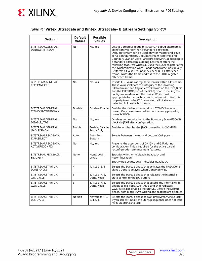
Table 41: Virtex UltraScale and Kintex UltraScale+ Bitstream Settings (cont'd)
Setting DefaultValues
PossibleValues Description
BITSTREAM.GENERAL.DEBUGBITSTREAM
No No, Yes Lets you create a debug bitstream. A debug bitstream issignificantly larger than a standard bitstream.DebugBitstream can be used only for master and slaveserial configurations. DebugBitstream is not valid forBoundary Scan or Slave Parallel/SelectMAP. In addition toa standard bitstream, a debug bitstream offers thefollowing features: Writes 32 0s to the LOUT register afterthe synchronization word. Loads each frame individually.Performs a Cyclic Redundancy Check (CRC) after eachframe. Writes the frame address to the LOUT registerafter each frame.
BITSTREAM.GENERAL.PERFRAMECRC
No No, Yes Inserts CRC values at regular intervals within bitstreams.These values validate the integrity of the incomingbitstream and can flag an error (shown on the INIT_B pinand the PRERROR port of the ICAP) prior to loading theconfiguration data into the device. While mostappropriate for partial bitstreams, when set to Yes, thisproperty inserts the CRC values into all bitstreams,including full device bitstreams.
BITSTREAM.GENERAL.SYSMONPOWERDOWN
Disable Disable, Enable Enables the device to power down SYSMON to savepower. Only recommended for permanently poweringdown SYSMON.
BITSTREAM.GENERAL.DISABLE_JTAG
No No, Yes Disables communication to the Boundary Scan (BSCAN)block via JTAG after configuration.
BITSTREAM.GENERAL.JTAG_SYSMON
Enable Enable, Disable,StatusOnly
Enables or disables the JTAG connection to SYSMON.
BITSTREAM.READBACK.ICAP_SELECT
Auto Auto, Top,Bottom
Selects between the top and bottom ICAP ports.
BITSTREAM.READBACK.ACTIVERECONFIG
No No, Yes Prevents the assertions of GHIGH and GSR duringconfiguration. This is required for the active partialreconfiguration enhancement features.
BITSTREAM. READBACK.SECURITY
None None, Level1,Level2
Specifies whether to disable Readback andReconfiguration.Specifying Security Level1 disables Readback.
BITSTREAM.STARTUP.DONE_CYCLE
4 4, 1, 2, 3, 5, 6 Selects the Startup phase that activates the FPGA Donesignal. Done is delayed when DonePipe=Yes.
BITSTREAM.STARTUP.GTS_CYCLE
5 5, 1, 2, 3, 4, 6,Done, Keep
Selects the Startup phase that releases the internal 3-state control to the I/O buffers.
BITSTREAM.STARTUP.GWE_CYCLE
6 6, 1, 2, 3, 4, 5,Done, Keep
Selects the Startup phase that asserts the internal writeenable to flip-flops, LUT RAMs, and shift registers.GWE_cycle also enables the BRAMS. Before the Startupphase, both block RAMs writing and reading are disabled.
BITSTREAM.STARTUP.LCK_CYCLE
NoWait NoWait, 0, 1, 2,3, 4, 5, 6
Selects the Startup phase to wait until MMCM/PLLs lock.If you select NoWait, the Startup sequence does not waitfor MMCM/PLLs to lock.
Appendix A: Device Configuration Bitstream or PDI Settings
UG908 (v2021.1) June 16, 2021 www.xilinx.comVivado Programming and Debugging 328Send Feedback
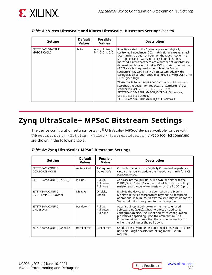
Table 41: Virtex UltraScale and Kintex UltraScale+ Bitstream Settings (cont'd)
Setting DefaultValues
PossibleValues Description
BITSTREAM.STARTUP.MATCH_CYCLE
Auto Auto, NoWait,0, 1, 2, 3, 4, 5, 6
Specifies a stall in the Startup cycle until digitallycontrolled impedance (DCI) match signals are asserted.DCI matching does not begin on the Match_cycle. TheStartup sequence waits in this cycle until DCI hasmatched. Given that there are a number of variables indetermining how long it takes DCI to match, the numberof CCLK cycles required to complete the Startupsequence may vary in any given system. Ideally, theconfiguration solution should continue driving CCLK untilDONE goes High.When the Auto setting is specified, write_bitstreamsearches the design for any DCI I/O standards. If DCIstandards exist, write_bitstream usesBITSTREAM.STARTUP.MATCH_CYCLE=2. Otherwise,write_bitstream usesBITSTREAM.STARTUP.MATCH_CYCLE=NoWait.
Zynq UltraScale+ MPSoC Bitstream SettingsThe device configuration settings for Zynq® UltraScale+ MPSoC devices available for use withthe set_property <Setting> <Value> [current_design] Vivado tool Tcl commandare shown in the following table.
Table 42: Zynq UltraScale+ MPSoC Bitstream Settings
Setting DefaultValues
PossibleValue Description
BITSTREAM.CONFIG.DCIUPDATEMODE
AsRequired AsRequired,Quiet, Safe
Controls how often the Digitally Controlled Impedancecircuit attempts to update the impedance match for DCIIOSTANDARDs.
BITSTREAM.CONFIG. PUDC_B Pullup Pullup,Pulldown,Pullnone
Adds an internal pull-up, pull-down, or neither to thePUDC_B pin. Select Pullnone to disable both the pull-upresistor and the pull-down resistor on the PUDC_B pin.
BITSTREAM.CONFIG.OVERTEMPSHUTDOWN
Disable Disable,Enable
Enables the device to shut down when the SystemMonitor detects a temperature beyond the acceptableoperational maximum. An external circuitry set up for theSystem Monitor is required to use this option.
BITSTREAM.CONFIG.UNUSEDPIN
Pulldown Pullup,Pulldown,Pullnone
Adds a pull-up, a pull-down, or neither to unusedSelectIO pins (IOBs). It has no effect on dedicatedconfiguration pins. The list of dedicated configurationpins varies depending upon the architecture. ThePullnone setting shows that there is no connection toeither the pull-up or the pull-down.
BITSTREAM.CONFIG. USERID 0xFFFFFFFF 0xFFFFFFFF Used to identify implementation revisions. You can enterup to an 8-digit hexadecimal string in the User IDregister.
Appendix A: Device Configuration Bitstream or PDI Settings
UG908 (v2021.1) June 16, 2021 www.xilinx.comVivado Programming and Debugging 329Send Feedback
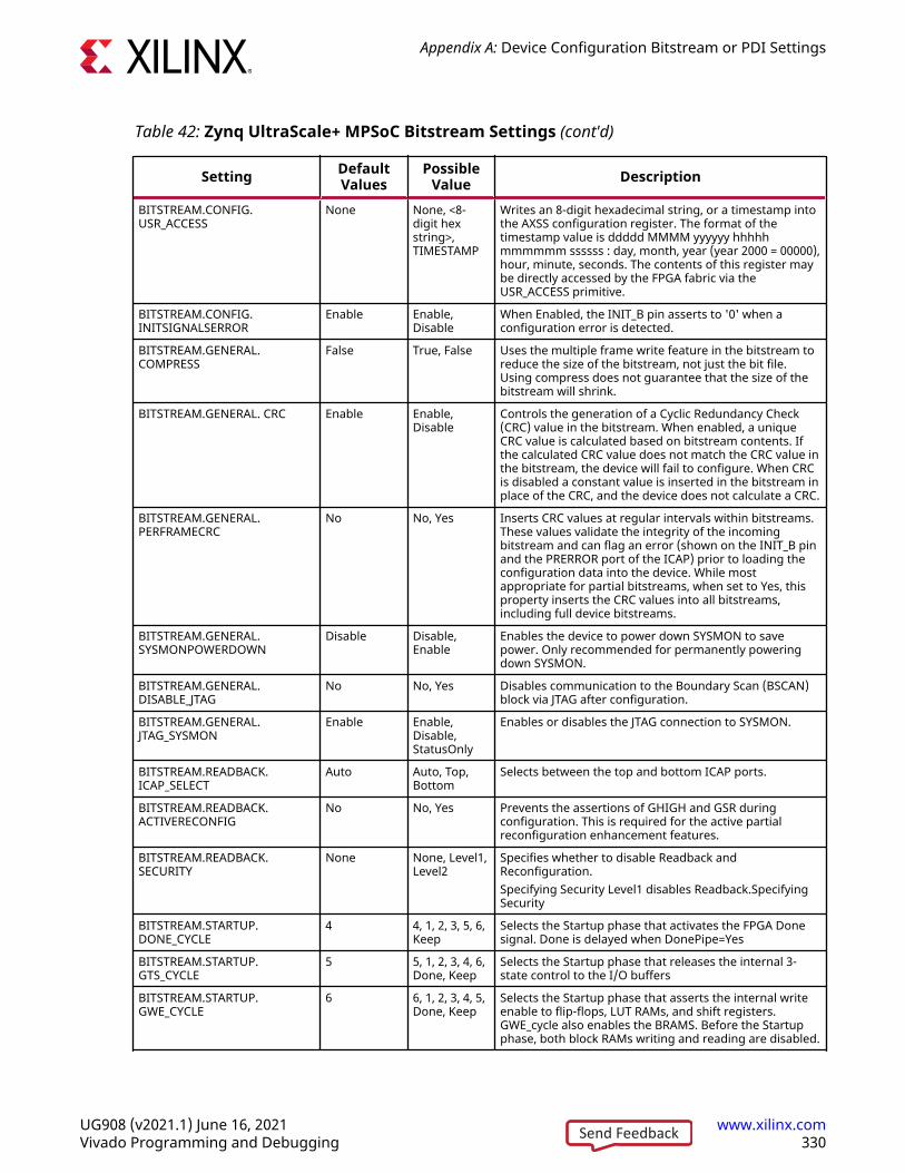
Table 42: Zynq UltraScale+ MPSoC Bitstream Settings (cont'd)
Setting DefaultValues
PossibleValue Description
BITSTREAM.CONFIG.USR_ACCESS
None None, <8-digit hexstring>,TIMESTAMP
Writes an 8-digit hexadecimal string, or a timestamp intothe AXSS configuration register. The format of thetimestamp value is ddddd MMMM yyyyyy hhhhhmmmmmm ssssss : day, month, year (year 2000 = 00000),hour, minute, seconds. The contents of this register maybe directly accessed by the FPGA fabric via theUSR_ACCESS primitive.
BITSTREAM.CONFIG.INITSIGNALSERROR
Enable Enable,Disable
When Enabled, the INIT_B pin asserts to '0' when aconfiguration error is detected.
BITSTREAM.GENERAL.COMPRESS
False True, False Uses the multiple frame write feature in the bitstream toreduce the size of the bitstream, not just the bit file.Using compress does not guarantee that the size of thebitstream will shrink.
BITSTREAM.GENERAL. CRC Enable Enable,Disable
Controls the generation of a Cyclic Redundancy Check(CRC) value in the bitstream. When enabled, a uniqueCRC value is calculated based on bitstream contents. Ifthe calculated CRC value does not match the CRC value inthe bitstream, the device will fail to configure. When CRCis disabled a constant value is inserted in the bitstream inplace of the CRC, and the device does not calculate a CRC.
BITSTREAM.GENERAL.PERFRAMECRC
No No, Yes Inserts CRC values at regular intervals within bitstreams.These values validate the integrity of the incomingbitstream and can flag an error (shown on the INIT_B pinand the PRERROR port of the ICAP) prior to loading theconfiguration data into the device. While mostappropriate for partial bitstreams, when set to Yes, thisproperty inserts the CRC values into all bitstreams,including full device bitstreams.
BITSTREAM.GENERAL.SYSMONPOWERDOWN
Disable Disable,Enable
Enables the device to power down SYSMON to savepower. Only recommended for permanently poweringdown SYSMON.
BITSTREAM.GENERAL.DISABLE_JTAG
No No, Yes Disables communication to the Boundary Scan (BSCAN)block via JTAG after configuration.
BITSTREAM.GENERAL.JTAG_SYSMON
Enable Enable,Disable,StatusOnly
Enables or disables the JTAG connection to SYSMON.
BITSTREAM.READBACK.ICAP_SELECT
Auto Auto, Top,Bottom
Selects between the top and bottom ICAP ports.
BITSTREAM.READBACK.ACTIVERECONFIG
No No, Yes Prevents the assertions of GHIGH and GSR duringconfiguration. This is required for the active partialreconfiguration enhancement features.
BITSTREAM.READBACK.SECURITY
None None, Level1,Level2
Specifies whether to disable Readback andReconfiguration.Specifying Security Level1 disables Readback.SpecifyingSecurity
BITSTREAM.STARTUP.DONE_CYCLE
4 4, 1, 2, 3, 5, 6,Keep
Selects the Startup phase that activates the FPGA Donesignal. Done is delayed when DonePipe=Yes
BITSTREAM.STARTUP.GTS_CYCLE
5 5, 1, 2, 3, 4, 6,Done, Keep
Selects the Startup phase that releases the internal 3-state control to the I/O buffers
BITSTREAM.STARTUP.GWE_CYCLE
6 6, 1, 2, 3, 4, 5,Done, Keep
Selects the Startup phase that asserts the internal writeenable to flip-flops, LUT RAMs, and shift registers.GWE_cycle also enables the BRAMS. Before the Startupphase, both block RAMs writing and reading are disabled.
Appendix A: Device Configuration Bitstream or PDI Settings
UG908 (v2021.1) June 16, 2021 www.xilinx.comVivado Programming and Debugging 330Send Feedback
Table 42: Zynq UltraScale+ MPSoC Bitstream Settings (cont'd)
Setting DefaultValues
PossibleValue Description
BITSTREAM.STARTUP.LCK_CYCLE
NoWait NoWait, 0, 1,2, 3, 4, 5, 6
Selects the Startup phase to wait until MMCM/PLLs lock.If you select NoWait, the Startup sequence does not waitfor MMCM/PLLs to lock.
BITSTREAM.STARTUP.MATCH_CYCLE
Auto Auto, NoWait,0, 1, 2, 3, 4, 5,6
Specifies a stall in the Startup cycle until digitallycontrolled impedance (DCI) match signals are asserted.DCI matching does not begin on the Match_cycle. TheStartup sequence waits in this cycle until DCI hasmatched. Given that there are a number of variables indetermining how long it takes DCI to match, the numberof CCLK cycles required to complete the Startupsequence may vary in any given system. Ideally, theconfiguration solution should continue driving CCLK untilDONE goes high.When the Auto setting is specified, write_bitstreamsearches the design for any DCI I/O standards. If DCIstandards exist, write_bitstream usesBITSTREAM.STARTUP.MATCH_CYCLE=2. Otherwise,write_bitstream usesBITSTREAM.STARTUP.MATCH_CYCLE=NoWait.
Versal ACAP Programmable Device Image(PDI) Settings
The device configuration settings for Versal ACAP devices are available for use with theset_property <Setting> <Value> [current_design] Vivado tool Tcl command areshown in the following table.
Note: On the Versal ACAP architecture, most programmable device image settings previously supported asa Bitstream setting are configured in either the Control, Interface, and Processing System (CIPS) IP or asBootgen settings. See the Control, Interface and Processing System LogiCORE IP Product Guide (PG352) or theBootgen User Guide (UG1283) for more information.
Table 43: Versal ACAP Programmable Device Image Settings
Setting Default Value PossibleValues Description
BITSTREAM.GENERAL.COMPRESS True True, False Use the run length encodingalgorithm to reduce the size of thePL configuration data. In most casesthis can reduce the size of the PLconfiguration data.
Appendix A: Device Configuration Bitstream or PDI Settings
UG908 (v2021.1) June 16, 2021 www.xilinx.comVivado Programming and Debugging 331Send Feedback
Table 43: Versal ACAP Programmable Device Image Settings (cont'd)
Setting Default Value PossibleValues Description
BITSTREAM.GENERAL.CRC False True, False Controls the generation of a CyclicRedundancy Check (CRC) value inthe PL portion of the PDI. Whenenabled, a unique CRC value iscalculated based on the PL portionof the PDI contents. If the calculatedCRC value does not match the CRCvalue in the PDI the device will failto configure.
BITSTREAM.GENERAL.PERFRAMECRC False True, False Inserts CRC values at regularintervals in the PL portion of thePDI. These values validate theintegrity of the incomingconfiguration data and can flag anerror prior to loading theconfiguration data into the device.While most appropriate for partialPDI's, when set to Yes this propertyinserts the CRC values into all PDI'sincluding full device images.
Appendix A: Device Configuration Bitstream or PDI Settings
UG908 (v2021.1) June 16, 2021 www.xilinx.comVivado Programming and Debugging 332Send Feedback
Appendix B
Trigger State Machine LanguageDescription
The trigger state machine language is used to describe complex trigger conditions that map tothe advanced trigger logic of the ILA debug core. The trigger state machine has the followingfeatures:
• Up to 16 states.
• One-, two-, and three-way conditional branching used for complex state transitions.
• Four built-in 16-bit counters used to count events, implement timers, etc.
• Four built-in flags used for monitoring trigger state machine execution status.
• Trigger action.
StatesEach state machine program can have up to 16 states declared. Each state is composed of a statedeclaration and a body:
state <state_name>: <state_body>
Goto ActionThe goto action is used to transition between states. Here is an example of using the gotoaction to transition from one state to another before triggering:
state my_state_0: goto my_state_1; state my_state_1: trigger;
Appendix B: Trigger State Machine Language Description
UG908 (v2021.1) June 16, 2021 www.xilinx.comVivado Programming and Debugging 333Send Feedback
Conditional BranchingThe trigger state machine language supports one-, two-, and three-way conditional branching perstate.
• One-way branching involves using goto actions without any if/elseif/else/endifconstructs:
state my_state_0: goto my_state_1;
• Two-way conditional branching uses goto actions with if/else/endif constructs:
state my_state_0: if (<condition1>) then goto my_state_1; else goto my_state_0; endif
• Three-way conditional branching uses goto actions with if/else/elseif/endifconstructs:
state my_state_0: if (<condition1>) then goto my_state_1; elseif (<condition2>) then goto my_state_2; else goto my_state_0; endif
For more information on how to construct conditional statements represented above with<condition1> and <condition2>, refer to the section Conditional Statements.
Related Information
Conditional Statements
CountersThe four built-in 16-bit counters have fixed names and are called $counter0, $counter1,$counter2, $counter3. The counters can be reset, incremented, and used in conditionalstatements.
Appendix B: Trigger State Machine Language Description
UG908 (v2021.1) June 16, 2021 www.xilinx.comVivado Programming and Debugging 334Send Feedback
• To reset a counter, use the reset_counter action:
state my_state_0: reset_counter $counter0; goto my_state_1;
• To increment a counter, use the increment_counter action:
state my_state_0: increment_counter $counter3; goto my_state_1;
For more information on how to use counters in conditional statements, refer to ConditionalStatements.
Related Information
Conditional Statements
FlagsFlags can be used to monitor progress of the trigger state machine program as it executes. Thefour built-in flags have fixed names and are called $flag0, $flag1, $flag2, and $flag3. Theflags can be set and cleared.
• To set a flag, use the set_flag action:
state my_state_0: set_flag $flag0; goto my_state_1;
• To clear a flag, use the clear_flag action:
state my_state_0: clear_flag $flag2; goto my_state_1;
Conditional StatementsDebug Probe ConditionsDebug probe conditions can be used in two-way and three-way branching conditionalstatements. Each debug probe condition consumes one trigger comparator on the PROBE port ofthe ILA to which the debug probe is attached.
Appendix B: Trigger State Machine Language Description
UG908 (v2021.1) June 16, 2021 www.xilinx.comVivado Programming and Debugging 335Send Feedback
IMPORTANT! Each PROBE port can have from 1 to 16 trigger comparators as configured at compile time.This means that you can only use a particular debug probe in a debug probe condition up from 1 to 16times in the entire trigger state machine program, depending on the number of comparators configured onthe PROBE port.
The debug probe conditions consist of a comparison operator and a value. The valid debug probecondition comparison operators are:
• == (equals)
• != (not equals)
• > (greater than)
• < (less than)
• >= (greater than or equal to)
• <= (less than or equal to)
Valid values are of the form:
<bit_width>'<radix><value>
Where:
• <bit width> is the width of the probe (in bits)
• <radix> is one of
○ b (binary)
○ h (hexadecimal)
○ u (unsigned decimal)
• <value> is one of
○ 0 (Logical zero)
○ 1 (Logical one)
○ X (dont care)
○ R (0-to-1 transition) - Valid only for 1 bit probes
○ F (1-to-0 transition) - Valid only for 1 bit probes
○ B (both transitions) - Valid only for 1 bit probes
○ N (No transitions) - Valid only for 1 bit probes
Examples of valid debug probe condition values are:
Appendix B: Trigger State Machine Language Description
UG908 (v2021.1) June 16, 2021 www.xilinx.comVivado Programming and Debugging 336Send Feedback
• 1-bit binary value of 0
1'b0
• 12-bit hex value of 7A
12'h07A
• 9-bit integer value of 123
9'u123
Examples of debug probe condition statements are:
• A single-bit debug probe called abc equals 0
if (abc == 1'b0) then
• A 23-bit debug probe xyz equals 456
if (xyz >= 23'u456) then
• A 23-bit debug probe klm does not equal hex A5
if (klm != 23'h0000A5) then
Examples of multiple debug probe condition statements are:
• Two debug probe comparisons combined with an "OR" function:
if ((xyz >= 23'u456) || (abc == 1'b0)) then
• Two debug probe comparisons combined with an "AND" function:
if ((xyz >= 23'u456) && (abc == 1'b0)) then
• Three debug probe comparisons combined with an "OR" function:
if ((xyz >= 23'u456) || (abc == 1'b0) || (klm != 23'h0000A5)) then
• Three debug probe comparisons combined with an "AND" function:
if ((xyz >= 23'u456) && (abc == 1'b0) && (klm != 23'h0000A5)) then
Counter ConditionsCounter conditions can be used in two-way and three-way branching conditional statements.Each counter condition consumes one counter comparator.
IMPORTANT! Each counter has only one counter comparator. This means that you can only use aparticular counter in a counter condition once in the entire trigger state machine program.
The probe port conditions consist of a comparison operator and a value. The valid probecondition comparison operators are:
Appendix B: Trigger State Machine Language Description
UG908 (v2021.1) June 16, 2021 www.xilinx.comVivado Programming and Debugging 337Send Feedback
• == (equals)
• != (not equals)
IMPORTANT! Each counter is always 16 bits wide.
Examples of valid counter condition values are:
• 16-bit binary value of 0
16'b0000_0000_0000_000016'b0000000000000000
• 16-bit hex value of 7A
16'h007A
• 16-bit integer value of 123
16'u123
Examples of counter condition statements:
• Counter $counter0 equals binary 0
($counter0 == 16'b0000000000000000)
• Counter $counter2 does not equal decimal 23
($counter2 != 16'u23)
Combined Debug Probe and Counter Conditions
Debug probe conditions and counter conditions can be combined together to form a singlecondition using the following rules:
• All debug probe comparisons must be combined together using the same "||" (OR) or "&&"(AND) operators.
• The combined debug probe condition can be combined with the counter condition usingeither the "||" (OR) or "&&" (AND) operators, regardless of the operator used to combine thedebug probe comparisons together.
Examples of multiple debug probe and counter condition statements are:
• Two debug probe comparisons combined with an "OR" function, then combined with counterconditional using "AND" function:
if (((xyz >= 23'u456) || (abc == 1'b0)) && ($counter0 == 16'u0023)) then
Appendix B: Trigger State Machine Language Description
UG908 (v2021.1) June 16, 2021 www.xilinx.comVivado Programming and Debugging 338Send Feedback
• Two debug probe comparisons combined with an "AND" function, then combined withcounter conditional using "OR" function:
if (((xyz >= 23'u456) && (abc == 1'b0)) || ($counter0 == 16'u0023)) then
• Three debug probe comparisons combined with an "OR" function, then combined withcounter conditional using "AND" function:
if (((xyz >= 23'u456) || (abc == 1'b0) || (klm != 23'h0000A5)) && ($counter0 == 16'u0023)) then
• Three debug probe comparisons combined with an "AND" function, then combined withcounter conditional using "OR" function:
if (((xyz >= 23'u456) && (abc == 1'b0) && (klm != 23'h0000A5)) || ($counter0 == 16'u0023)) then
Trigger State Machine Language GrammarNote:
• The language is case insensitive
• Comment character is hash '#' character. Anything including and after a # character is ignored.
• 'THING' = THING is a terminal
• {<thing>} = 0 or more thing
• [<thing>] = 0 or 1 thing
<program> ::= <state_list><state_list> ::= <state_list> <state> | <state><state> ::= 'STATE' <state_label> ':' <if_condition> | <action_block>
<action_block> ::= <action_list> 'GOTO' <state_label> ';'| <action_list> 'TRIGGER' ';'| 'GOTO' <state_label> ';'| 'TRIGGER' ';'<action_list> ::= <action_statement> | <action_list> <action_statement><action_statement> ::= 'SET_FLAG' <flag_name> ';'| 'CLEAR_FLAG' <flag_name> ';'| 'INCREMENT_COUNTER' <counter_name> ';'| 'RESET_COUNTER' <counter_name> ';'<if_condition> ::= 'IF' '(' <condition> ')' 'THEN' <actionblock> ['ELSEIF' '(' <condition> ')' 'THEN' <actionblock>] 'ELSE' <actionblock> 'ENDIF'<condition> ::= <probe_match_list>| <counter_match>| <probe_counter_match><probe_counter_match> ::= '(' <probe_counter_match> ')'| <probe_match_list> <boolean_logic_op> <counter_match>| <counter_match> <boolean_logic_op> <probe_match_list><probe_match_list> ::= '(' <probe_match> ')'| <probe_match><probe_match> ::= <probe_match_list> <boolean_logic_op> <probe_match_list>
Appendix B: Trigger State Machine Language Description
UG908 (v2021.1) June 16, 2021 www.xilinx.comVivado Programming and Debugging 339Send Feedback
| <probe_name> <compare_op> <constant>| <constant> <compare_op> <probe_name><counter_match> ::= '(' <counter_match> ')'| <counter_name> <compare_op> <constant>| <constant> <compare_op> <counter_name><constant> ::= <integer_constant>| <hex_constant>| <binary_constant><compare_op> ::= '==' | '!=' | '>' | '>=' | '<' | '<='<boolean_logic_op> ::= '&&' | '||'--- The following are in regular expression format to simplify expressions:--- [A-Z0-9] means match any single character in AB...Z,0..9--- [AB]+ means match [AB] one or more times like A, AB, ABAB, AAA, etc--- [AB]* means match [AB] zero or more times<probe_name> ::= [A-Z_\[\]<>/][A-Z_0-9\[\]<>/]+<state_label> ::= [A-Z_][A-Z_0-9]+<flag_name> ::= \$FLAG[0-3]<counter_name> ::= \$COUNTER[0-3]<hex_constant> ::= <integer>*'h<hex_digit>+<binary_constant> ::= <integer>*'b<binary_digit>+<integer_constant> ::= <integer>*'u<integer_digit>+<integer> ::= <digit>+<hex_digit> ::= [0-9ABCDEFBN_]<binary_digit> ::= [01XRFBN_]<digit> ::= [0-9]
Appendix B: Trigger State Machine Language Description
UG908 (v2021.1) June 16, 2021 www.xilinx.comVivado Programming and Debugging 340Send Feedback
Appendix C
Low Level SVF JTAG CommandsNote: SVF is not supported on Versal™ devices.
Low level JTAG commands allow you to scan multiple FPGA JTAG chains. The SVF commandsgenerated for chain operations use these low-level commands to access the FPGAs in the chain.
This appendix is an overview of these commands. A detailed explanation can be found in theSerial Vector Format Specification document that can be found at: http://www.jtagtest.com/pdf/svf_specification.pdf.
Header Data Register (HDR), HeaderInstruction Register (HIR)
SyntaxHDR length [TDI (tdi)] [TDO (tdo)] [MASK (mask)] [SMASK (smask)];HIR length [TDI (tdi)] [TDO (tdo)] [MASK (mask)] [SMASK (smask)];
PurposeSpecifies a default header pattern that is shifted in before every scan operation. The headerpattern specifies how to pad the scan statements with a set of leading bits that accommodate thedevices located on the scan path beyond the component of interest.
General InformationThe Header Data Register (HDR) specifies a default header pattern that is pre-pended to thebeginning of all subsequent SDR commands. The Header Instruction Register (HIR) specifies adefault header pattern that is pre-pended to the beginning of all subsequent SIR commands. Theheader commands have a set of counterpart trailer commands (TIR, TDR) that are described in afollowing section. A header can be removed by setting its length to 0.
Appendix C: Low Level SVF JTAG Commands
UG908 (v2021.1) June 16, 2021 www.xilinx.comVivado Programming and Debugging 341Send Feedback
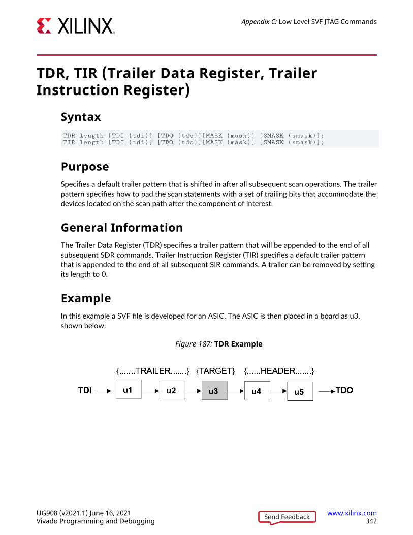
TDR, TIR (Trailer Data Register, TrailerInstruction Register)
SyntaxTDR length [TDI (tdi)] [TDO (tdo)][MASK (mask)] [SMASK (smask)]; TIR length [TDI (tdi)] [TDO (tdo)][MASK (mask)] [SMASK (smask)];
PurposeSpecifies a default trailer pattern that is shifted in after all subsequent scan operations. The trailerpattern specifies how to pad the scan statements with a set of trailing bits that accommodate thedevices located on the scan path after the component of interest.
General InformationThe Trailer Data Register (TDR) specifies a trailer pattern that will be appended to the end of allsubsequent SDR commands. Trailer Instruction Register (TIR) specifies a default trailer patternthat is appended to the end of all subsequent SIR commands. A trailer can be removed by settingits length to 0.
ExampleIn this example a SVF file is developed for an ASIC. The ASIC is then placed in a board as u3,shown below:
Figure 187: TDR Example
Appendix C: Low Level SVF JTAG Commands
UG908 (v2021.1) June 16, 2021 www.xilinx.comVivado Programming and Debugging 342Send Feedback
The set of SVF statements originally developed for the ASIC can be reused with minimalmodification if the appropriate header and trailer statements are defined to accommodate thedevices in front of and behind u3. In this example, a header pattern would be defined for devicesu4 and u5, and a trailer pattern would be defined for u2 and u1. The optional parameters can bespecified in any order. Each optional parameter can only be specified once. Hex strings specifiedfor TDI, TDO, MASK, or SMASK cannot be a value larger than the maximum implied by thelength parameter. Leading zeros are assumed for a hex string if not explicitly specified.
scan_ir_hwPerform shift IR on hw_jtag.
Syntaxscan_ir_hw_jtag [-tdi <arg>] [-tdo <arg>] [-mask <arg>] [-smask <arg>] [-quiet] [-verbose] <length>
General InformationThe scan_ir_hw_jtag command specifies a scan pattern to be scanned into the JTAGinterface target instruction register. The command targets a hw_jtag object which is createdwhen the hw_target is opened in JTAG mode through the use of the open_hw_target -jtag_mode command. When targeting the hw_jtag object prior to shifting the scan patternspecified in the scan_ir_hw_jtag command, the last defined header property (HIR) is pre-pendedto the beginning of the specified data pattern. The last defined trailer property (TIR) is appendedto the end of the data pattern.
The number of bits represented by the hex strings specified for -tdi, -tdo, -mask, or -smaskcannot be greater than the maximum specified by <length>.
The scan_ir_hw_jtag command returns a hex array containing captured TDO data from thehw_jtag, or returns an error if it fails.
ExampleThe following example scans the JTAG instruction register for a 24 bit value:
scan_ir_hw_jtag 24
Appendix C: Low Level SVF JTAG Commands
UG908 (v2021.1) June 16, 2021 www.xilinx.comVivado Programming and Debugging 343Send Feedback
The following example sends a 24 bit value 0x00_0010 (LSB first) to TDI, then captures the TDOoutput, applies a mask with 0xF3_FFFF, and compares the returned TDO value against thespecified value -tdo 0x81_8181.
scan_ir_hw_jtag 24 -tdi 000010 -tdo 818181 -mask F3FFFF -smask 0
scan_dr_hwPerform shift DR on 'hw_jtag'.
Syntaxscan_dr_hw_jtag [-tdi <arg>] [-tdo <arg>] [-mask <arg>] [-smask <arg>] [-quiet] [-verbose] <length>
General InformationThe scan_dr_hw_jtag command specifies a scan pattern to be scanned into the JTAGinterface target data register. The command targets a hw_jtag object which is created when thehw_target is opened in JTAG mode through the use of the open_hw_target -jtag_modecommand. When targeting the hw_jtag object prior to shifting the scan pattern specified in thescan_dr_hw_jtag command, the last defined header property (HDR) is pre-pended to thebeginning of the specified data pattern. The last defined trailer property (TDR) is appended to theend of the data pattern.
The scan_dr_hw_jtag command returns a hex array containing captured TDO data from thehw_jtag, or returns an error if it fails.
ExampleThe following example scans the JTAG data register for a 24 bit value:
scan_dr_hw_jtag 24
The following example sends a 24 bit value 0x00_0010 (LSB first) to TDI, then captures the dataoutput, TDO, applies a mask with 0xF3_FFFF, and compares the returned TDO value against thespecified value -tdo 0x81_8181.
scan_dr_hw_jtag 24 -tdi 000010 -tdo 818181 -mask F3FFFF -smask 0
Appendix C: Low Level SVF JTAG Commands
UG908 (v2021.1) June 16, 2021 www.xilinx.comVivado Programming and Debugging 344Send Feedback
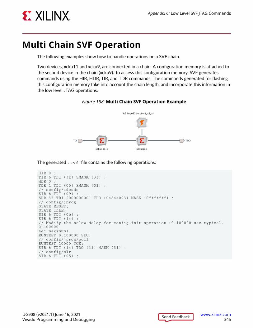
Multi Chain SVF OperationThe following examples show how to handle operations on a SVF chain.
Two devices, xcku11 and xcku9, are connected in a chain. A configuration memory is attached tothe second device in the chain (xcku9). To access this configuration memory, SVF generatescommands using the HIR, HDR, TIR, and TDR commands. The commands generated for flashingthis configuration memory take into account the chain length, and incorporate this information inthe low level JTAG operations.
Figure 188: Multi Chain SVF Operation Example
The generated .svf file contains the following operations:
HIR 0 ;TIR 6 TDI (3f) SMASK (3f) ;HDR 0 ;TDR 1 TDI (00) SMASK (01) ;// config/idcodeSIR 6 TDI (09) ;SDR 32 TDI (00000000) TDO (0484a093) MASK (0fffffff) ;// config/jprogSTATE RESET;STATE IDLE;SIR 6 TDI (0b) ;SIR 6 TDI (14) ;// Modify the below delay for config_init operation (0.100000 sec typical, 0.100000 sec maximum)RUNTEST 0.100000 SEC;// config/jprog/pollRUNTEST 10000 TCK;SIR 6 TDI (14) TDO (11) MASK (31) ;// config/slrSIR 6 TDI (05) ;
Appendix C: Low Level SVF JTAG Commands
UG908 (v2021.1) June 16, 2021 www.xilinx.comVivado Programming and Debugging 345Send Feedback
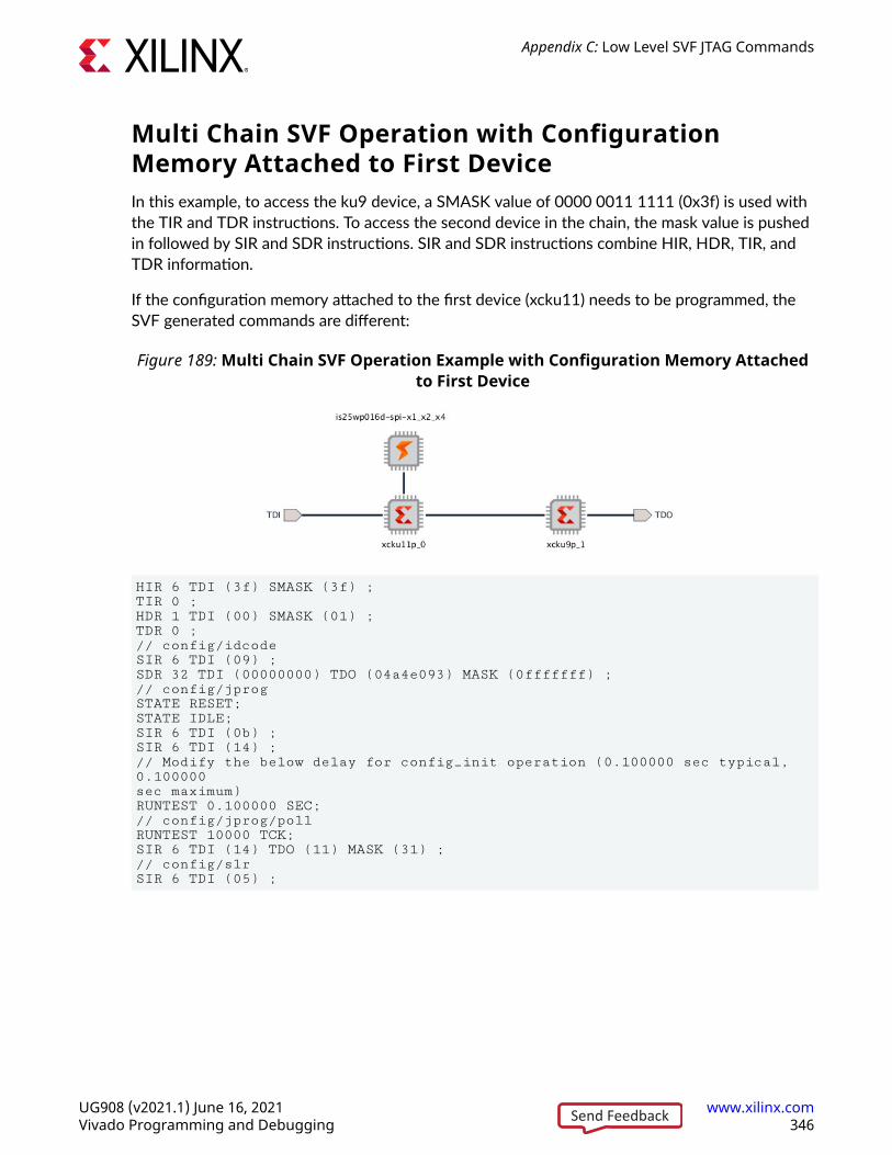
Multi Chain SVF Operation with ConfigurationMemory Attached to First DeviceIn this example, to access the ku9 device, a SMASK value of 0000 0011 1111 (0x3f) is used withthe TIR and TDR instructions. To access the second device in the chain, the mask value is pushedin followed by SIR and SDR instructions. SIR and SDR instructions combine HIR, HDR, TIR, andTDR information.
If the configuration memory attached to the first device (xcku11) needs to be programmed, theSVF generated commands are different:
Figure 189: Multi Chain SVF Operation Example with Configuration Memory Attachedto First Device
HIR 6 TDI (3f) SMASK (3f) ;TIR 0 ;HDR 1 TDI (00) SMASK (01) ;TDR 0 ;// config/idcodeSIR 6 TDI (09) ;SDR 32 TDI (00000000) TDO (04a4e093) MASK (0fffffff) ;// config/jprogSTATE RESET;STATE IDLE;SIR 6 TDI (0b) ;SIR 6 TDI (14) ;// Modify the below delay for config_init operation (0.100000 sec typical, 0.100000 sec maximum)RUNTEST 0.100000 SEC;// config/jprog/pollRUNTEST 10000 TCK;SIR 6 TDI (14) TDO (11) MASK (31) ;// config/slrSIR 6 TDI (05) ;
Appendix C: Low Level SVF JTAG Commands
UG908 (v2021.1) June 16, 2021 www.xilinx.comVivado Programming and Debugging 346Send Feedback
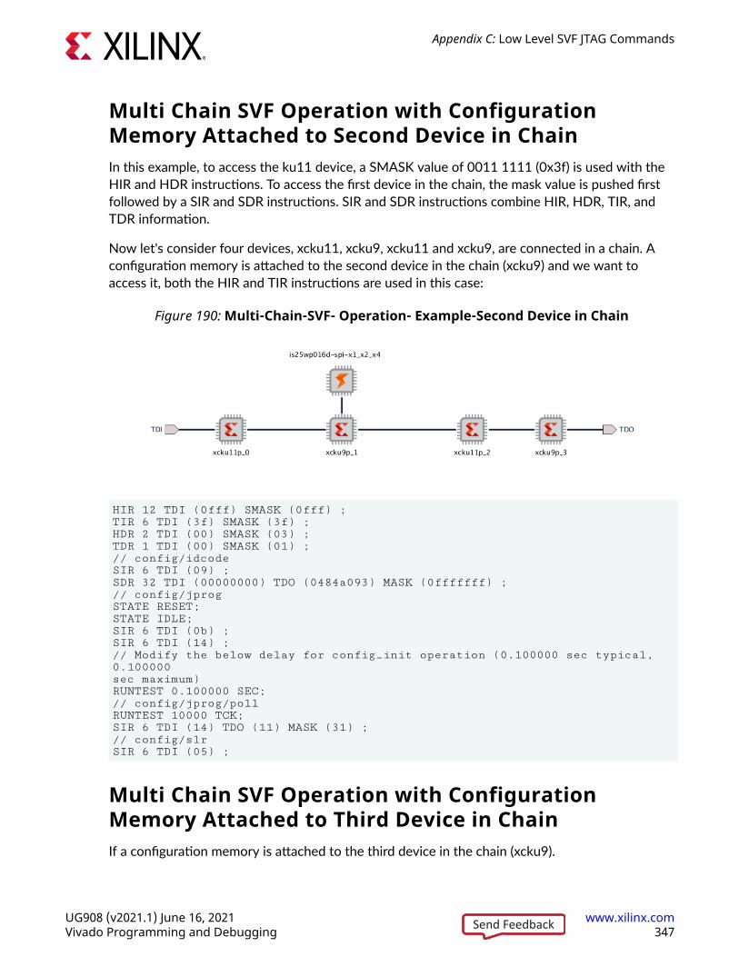
Multi Chain SVF Operation with ConfigurationMemory Attached to Second Device in ChainIn this example, to access the ku11 device, a SMASK value of 0011 1111 (0x3f) is used with theHIR and HDR instructions. To access the first device in the chain, the mask value is pushed firstfollowed by a SIR and SDR instructions. SIR and SDR instructions combine HIR, HDR, TIR, andTDR information.
Now let's consider four devices, xcku11, xcku9, xcku11 and xcku9, are connected in a chain. Aconfiguration memory is attached to the second device in the chain (xcku9) and we want toaccess it, both the HIR and TIR instructions are used in this case:
Figure 190: Multi-Chain-SVF- Operation- Example-Second Device in Chain
HIR 12 TDI (0fff) SMASK (0fff) ;TIR 6 TDI (3f) SMASK (3f) ;HDR 2 TDI (00) SMASK (03) ;TDR 1 TDI (00) SMASK (01) ;// config/idcodeSIR 6 TDI (09) ;SDR 32 TDI (00000000) TDO (0484a093) MASK (0fffffff) ;// config/jprogSTATE RESET;STATE IDLE;SIR 6 TDI (0b) ;SIR 6 TDI (14) ;// Modify the below delay for config_init operation (0.100000 sec typical, 0.100000 sec maximum)RUNTEST 0.100000 SEC;// config/jprog/pollRUNTEST 10000 TCK;SIR 6 TDI (14) TDO (11) MASK (31) ;// config/slrSIR 6 TDI (05) ;
Multi Chain SVF Operation with ConfigurationMemory Attached to Third Device in ChainIf a configuration memory is attached to the third device in the chain (xcku9).
Appendix C: Low Level SVF JTAG Commands
UG908 (v2021.1) June 16, 2021 www.xilinx.comVivado Programming and Debugging 347Send Feedback
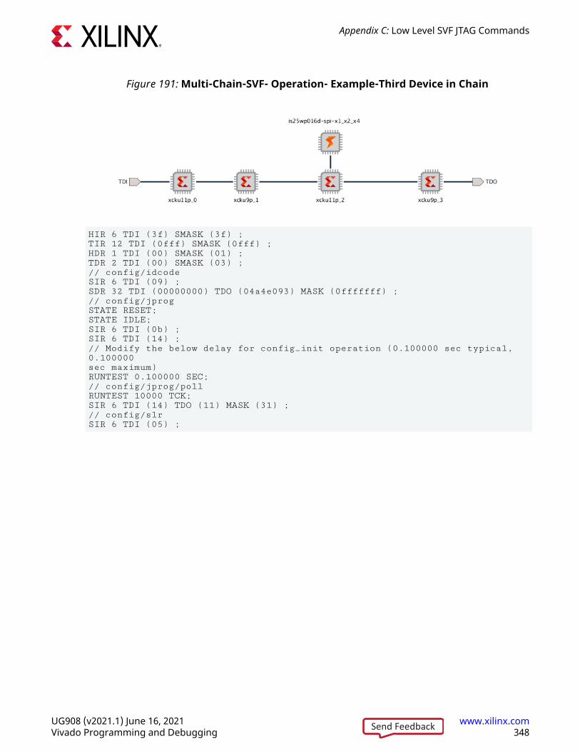
Figure 191: Multi-Chain-SVF- Operation- Example-Third Device in Chain
HIR 6 TDI (3f) SMASK (3f) ;TIR 12 TDI (0fff) SMASK (0fff) ;HDR 1 TDI (00) SMASK (01) ;TDR 2 TDI (00) SMASK (03) ;// config/idcodeSIR 6 TDI (09) ;SDR 32 TDI (00000000) TDO (04a4e093) MASK (0fffffff) ;// config/jprogSTATE RESET;STATE IDLE;SIR 6 TDI (0b) ;SIR 6 TDI (14) ;// Modify the below delay for config_init operation (0.100000 sec typical, 0.100000 sec maximum)RUNTEST 0.100000 SEC;// config/jprog/pollRUNTEST 10000 TCK;SIR 6 TDI (14) TDO (11) MASK (31) ;// config/slrSIR 6 TDI (05) ;
Appendix C: Low Level SVF JTAG Commands
UG908 (v2021.1) June 16, 2021 www.xilinx.comVivado Programming and Debugging 348Send Feedback
Appendix D
JTAG Cables and Devices Supportedby hw_server
The list of compatible JTAG download cables and devices that are supported by hw_server are:
• Xilinx® SmartLynq+ Module (HW-SMARTLYNQ-PLUS-G)
• Xilinx® SmartLynq Data Cable (HW-SMARTLYNQ-G/DLC20)
• Xilinx® Platform Cable USB II (DLC10)
• Xilinx® Platform Cable USB (DLC9G, DLC9LP, DLC9)
• Digilent JTAG-HS1
• Digilent JTAG-HS2
• Digilent JTAG-HS3
• Digilent JTAG-SMT1
• Digilent JTAG-SMT2
Appendix D: JTAG Cables and Devices Supported by hw_server
UG908 (v2021.1) June 16, 2021 www.xilinx.comVivado Programming and Debugging 349Send Feedback
Appendix E
Configuration Memory SupportThis section covers the various non-volatile device memories that are supported by Vivado®
software. Use this section as a guide to select the appropriate configuration memory device foryour application by Xilinx® family, interface, manufacturer, density, and data width.
Artix-7 Configuration Memory DevicesThe Flash devices supported for configuration of Artix®-7 devices that can be erased, blankchecked, programmed, and verified by Vivado® software are shown in the following table.
The tables in this Appendix are running lists per Xilinx® family of non-volatile memories whichVivado software is capable of erasing, blank checking, programming, and verifying. Xilinx strivesto retain components on this list even after they are no longer appropriate for new designs, tosupport long-term maintenance of end products which may contain them.
IMPORTANT! Given the evolving nature of the commodity non-volatile memory market, Xilinxrecommends contacting your non-volatile memory supplier to confirm device availability and life cycle.References to specific devices in the tables are not an assurance of their current or future availability.
Table 44: Supported Flash Memory Devices for Artix-7 Memory Devices
Interface Manufacturer ManufacturerFamily Device Alias Density
MbitsData Width
BitsBPI Micron g18 28f128g18f 128 x16
BPI Micron g18 mt28gu256aax1e [28f256g18f-bpi-x16] 256 x16
BPI Micron g18 mt28gu512aax1e [28f512g18f-bpi-x16] 512 x16
BPI Micron g18 mt28gu01gaax1e [28f00ag18f-bpi-x16] 1,024 x16
BPI Micron m29ew 28f064m29ewb 64 x16, x8
BPI Micron m29ew 28f064m29ewh 64 x16, x8
BPI Micron m29ew 28f064m29ewl 64 x16, x8
BPI Micron m29ew 28f064m29ewt 64 x16, x8
BPI Micron m29ew 28f128m29ew 128 x16, x8
BPI Micron m29ew 28f256m29ew 256 x16, x8
BPI Micron m29ew 28f512m29ew 512 x16, x8
BPI Micron m29ew 28f00am29ew 1,024 x16, x8
Appendix E: Configuration Memory Support
UG908 (v2021.1) June 16, 2021 www.xilinx.comVivado Programming and Debugging 350Send Feedback

Table 44: Supported Flash Memory Devices for Artix-7 Memory Devices (cont'd)
Interface Manufacturer ManufacturerFamily Device Alias Density
MbitsData Width
BitsBPI Micron m29ew 28f00bm29ew 2,048 x16, x8
BPI Micron m29w m29w640gh 64 x16, x8
BPI Micron m29w m29w640gl 64 x16, x8
BPI Micron m29w m29w128gh 128 x16, x8
BPI Micron m29w m29w128gl 128 x16, x8
BPI Micron m29w m29w256gh 256 x16, x8
BPI Micron m29w m29w256gl 256 x16, x8
BPI Micron mt28ew mt28ew128a 128 x16, x8
BPI Micron mt28ew mt28ew256a 256 x16, x8
BPI Micron mt28ew mt28ew512a 512 x16, x8
BPI Micron mt28ew mt28ew01ga 1,024 x16, x8
BPI Micron mt28fw mt28fw02gb 2,048 x16
BPI Micron p30 28f640p30b 64 x16
BPI Micron p30 28f640p30t 64 x16
BPI Micron p30 28f128p30b 128 x16
BPI Micron p30 28f128p30t 128 x16
BPI Micron p30 28f256p30b 256 x16
BPI Micron p30 28f256p30t 256 x16
BPI Micron p30 28f512p30b 512 x16
BPI Micron p30 28f512p30e 512 x16
BPI Micron p30 28f512p30t 512 x16
BPI Micron p30 28f00ap30b 1,024 x16
BPI Micron p30 28f00ap30e 1,024 x16
BPI Micron p30 28f00ap30t 1,024 x16
BPI Micron p30 28f00bp30e 2,048 x16
BPI Micron p33 28f640p33b 64 x16
BPI Micron p33 28f640p33t 64 x16
BPI Micron p33 28f128p33b 128 x16
BPI Micron p33 28f128p33t 128 x16
BPI Micron p33 28f256p33b 256 x16
BPI Micron p33 28f256p33t 256 x16
BPI Micron p33 28f512p33b 512 x16
BPI Micron p33 28f512p33e 512 x16
BPI Micron p33 28f512p33t 512 x16
BPI Micron p33 28f00ap33b 1,024 x16
BPI Micron p33 28f00ap33e 1,024 x16
BPI Micron p33 28f00ap33t 1,024 x16
Appendix E: Configuration Memory Support
UG908 (v2021.1) June 16, 2021 www.xilinx.comVivado Programming and Debugging 351Send Feedback
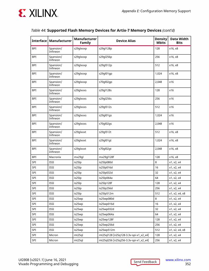
Table 44: Supported Flash Memory Devices for Artix-7 Memory Devices (cont'd)
Interface Manufacturer ManufacturerFamily Device Alias Density
MbitsData Width
BitsBPI Spansion/
Infineons29glxxxp s29gl128p 128 x16, x8
BPI Spansion/Infineon
s29glxxxp s29gl256p 256 x16, x8
BPI Spansion/Infineon
s29glxxxp s29gl512p 512 x16, x8
BPI Spansion/Infineon
s29glxxxp s29gl01gp 1,024 x16, x8
BPI Spansion/Infineon
s29glxxxp s70gl02gp 2,048 x16
BPI Spansion/Infineon
s29glxxxs s29gl128s 128 x16
BPI Spansion/Infineon
s29glxxxs s29gl256s 256 x16
BPI Spansion/Infineon
s29glxxxs s29gl512s 512 x16
BPI Spansion/Infineon
s29glxxxs s29gl01gs 1,024 x16
BPI Spansion/Infineon
s29glxxxs s70gl02gs 2,048 x16
BPI Spansion/Infineon
s29glxxxt s29gl512t 512 x16, x8
BPI Spansion/Infineon
s29glxxxt s29gl01gt 1,024 x16, x8
BPI Spansion/Infineon
s29glxxxt s70gl02gt 2,048 x16, x8
BPI Macronix mx29gl mx29gl128f 128 x16, x8
SPI ISSI is25lp is25lp080d 8 x1, x2, x4
SPI ISSI is25lp is25lp016d 16 x1, x2, x4
SPI ISSI is25lp is25lp032d 32 x1, x2, x4
SPI ISSI is25lp is25lp064a 64 x1, x2, x4
SPI ISSI is25lp is25lp128f 128 x1, x2, x4
SPI ISSI is25lp is25lp256d 256 x1, x2, x4
SPI ISSI is25lp is25lp512m 512 x1, x2, x4, x8
SPI ISSI is25wp is25wp080d 8 x1, x2, x4
SPI ISSI is25wp is25wp016d 16 x1, x2, x4
SPI ISSI is25wp is25wp032d 32 x1, x2, x4
SPI ISSI is25wp is25wp064a 64 x1, x2, x4
SPI ISSI is25wp is25wp128f 128 x1, x2, x4
SPI ISSI is25wp is25wp256d 256 x1, x2, x4
SPI ISSI is25wp is25wp512m 512 x1, x2, x4, x8
SPI Micron mt25ql mt25ql128 [n25q128-3.3v-spi-x1_x2_x4] 128 x1, x2, x4
SPI Micron mt25ql mt25ql256 [n25q256-3.3v-spi-x1_x2_x4] 256 x1, x2, x4
Appendix E: Configuration Memory Support
UG908 (v2021.1) June 16, 2021 www.xilinx.comVivado Programming and Debugging 352Send Feedback
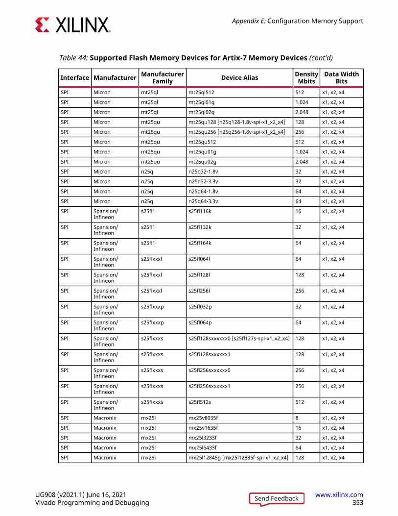
Table 44: Supported Flash Memory Devices for Artix-7 Memory Devices (cont'd)
Interface Manufacturer ManufacturerFamily Device Alias Density
MbitsData Width
BitsSPI Micron mt25ql mt25ql512 512 x1, x2, x4
SPI Micron mt25ql mt25ql01g 1,024 x1, x2, x4
SPI Micron mt25ql mt25ql02g 2,048 x1, x2, x4
SPI Micron mt25qu mt25qu128 [n25q128-1.8v-spi-x1_x2_x4] 128 x1, x2, x4
SPI Micron mt25qu mt25qu256 [n25q256-1.8v-spi-x1_x2_x4] 256 x1, x2, x4
SPI Micron mt25qu mt25qu512 512 x1, x2, x4
SPI Micron mt25qu mt25qu01g 1,024 x1, x2, x4
SPI Micron mt25qu mt25qu02g 2,048 x1, x2, x4
SPI Micron n25q n25q32-1.8v 32 x1, x2, x4
SPI Micron n25q n25q32-3.3v 32 x1, x2, x4
SPI Micron n25q n25q64-1.8v 64 x1, x2, x4
SPI Micron n25q n25q64-3.3v 64 x1, x2, x4
SPI Spansion/Infineon
s25fl1 s25fl116k 16 x1, x2, x4
SPI Spansion/Infineon
s25fl1 s25fl132k 32 x1, x2, x4
SPI Spansion/Infineon
s25fl1 s25fl164k 64 x1, x2, x4
SPI Spansion/Infineon
s25flxxxl s25fl064l 64 x1, x2, x4
SPI Spansion/Infineon
s25flxxxl s25fl128l 128 x1, x2, x4
SPI Spansion/Infineon
s25flxxxl s25fl256l 256 x1, x2, x4
SPI Spansion/Infineon
s25flxxxp s25fl032p 32 x1, x2, x4
SPI Spansion/Infineon
s25flxxxp s25fl064p 64 x1, x2, x4
SPI Spansion/Infineon
s25flxxxs s25fl128sxxxxxx0 [s25fl127s-spi-x1_x2_x4] 128 x1, x2, x4
SPI Spansion/Infineon
s25flxxxs s25fl128sxxxxxx1 128 x1, x2, x4
SPI Spansion/Infineon
s25flxxxs s25fl256sxxxxxx0 256 x1, x2, x4
SPI Spansion/Infineon
s25flxxxs s25fl256sxxxxxx1 256 x1, x2, x4
SPI Spansion/Infineon
s25flxxxs s25fl512s 512 x1, x2, x4
SPI Macronix mx25l mx25v8035f 8 x1, x2, x4
SPI Macronix mx25l mx25v1635f 16 x1, x2, x4
SPI Macronix mx25l mx25l3233f 32 x1, x2, x4
SPI Macronix mx25l mx25l6433f 64 x1, x2, x4
SPI Macronix mx25l mx25l12845g [mx25l12835f-spi-x1_x2_x4] 128 x1, x2, x4
Appendix E: Configuration Memory Support
UG908 (v2021.1) June 16, 2021 www.xilinx.comVivado Programming and Debugging 353Send Feedback
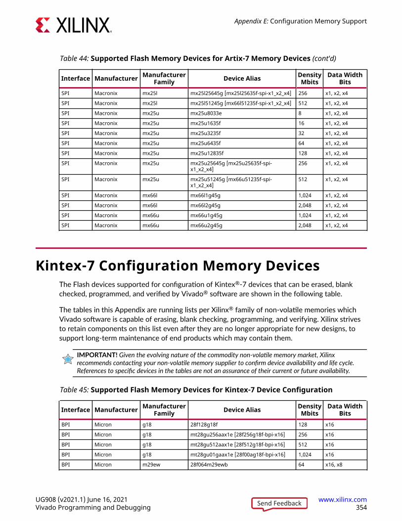
Table 44: Supported Flash Memory Devices for Artix-7 Memory Devices (cont'd)
Interface Manufacturer ManufacturerFamily Device Alias Density
MbitsData Width
BitsSPI Macronix mx25l mx25l25645g [mx25l25635f-spi-x1_x2_x4] 256 x1, x2, x4
SPI Macronix mx25l mx25l51245g [mx66l51235f-spi-x1_x2_x4] 512 x1, x2, x4
SPI Macronix mx25u mx25u8033e 8 x1, x2, x4
SPI Macronix mx25u mx25u1635f 16 x1, x2, x4
SPI Macronix mx25u mx25u3235f 32 x1, x2, x4
SPI Macronix mx25u mx25u6435f 64 x1, x2, x4
SPI Macronix mx25u mx25u12835f 128 x1, x2, x4
SPI Macronix mx25u mx25u25645g [mx25u25635f-spi-x1_x2_x4]
256 x1, x2, x4
SPI Macronix mx25u mx25u51245g [mx66u51235f-spi-x1_x2_x4]
512 x1, x2, x4
SPI Macronix mx66l mx66l1g45g 1,024 x1, x2, x4
SPI Macronix mx66l mx66l2g45g 2,048 x1, x2, x4
SPI Macronix mx66u mx66u1g45g 1,024 x1, x2, x4
SPI Macronix mx66u mx66u2g45g 2,048 x1, x2, x4
Kintex-7 Configuration Memory DevicesThe Flash devices supported for configuration of Kintex®-7 devices that can be erased, blankchecked, programmed, and verified by Vivado® software are shown in the following table.
The tables in this Appendix are running lists per Xilinx® family of non-volatile memories whichVivado software is capable of erasing, blank checking, programming, and verifying. Xilinx strivesto retain components on this list even after they are no longer appropriate for new designs, tosupport long-term maintenance of end products which may contain them.
IMPORTANT! Given the evolving nature of the commodity non-volatile memory market, Xilinxrecommends contacting your non-volatile memory supplier to confirm device availability and life cycle.References to specific devices in the tables are not an assurance of their current or future availability.
Table 45: Supported Flash Memory Devices for Kintex-7 Device Configuration
Interface Manufacturer ManufacturerFamily Device Alias Density
MbitsData Width
BitsBPI Micron g18 28f128g18f 128 x16
BPI Micron g18 mt28gu256aax1e [28f256g18f-bpi-x16] 256 x16
BPI Micron g18 mt28gu512aax1e [28f512g18f-bpi-x16] 512 x16
BPI Micron g18 mt28gu01gaax1e [28f00ag18f-bpi-x16] 1,024 x16
BPI Micron m29ew 28f064m29ewb 64 x16, x8
Appendix E: Configuration Memory Support
UG908 (v2021.1) June 16, 2021 www.xilinx.comVivado Programming and Debugging 354Send Feedback
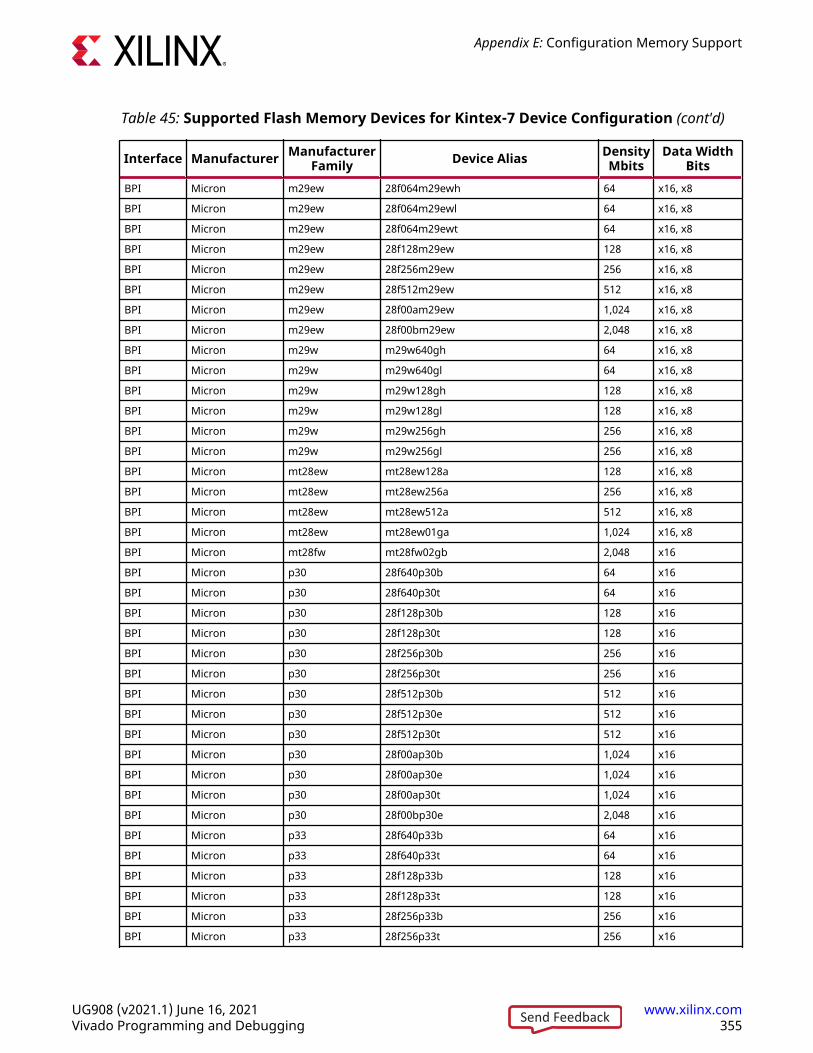
Table 45: Supported Flash Memory Devices for Kintex-7 Device Configuration (cont'd)
Interface Manufacturer ManufacturerFamily Device Alias Density
MbitsData Width
BitsBPI Micron m29ew 28f064m29ewh 64 x16, x8
BPI Micron m29ew 28f064m29ewl 64 x16, x8
BPI Micron m29ew 28f064m29ewt 64 x16, x8
BPI Micron m29ew 28f128m29ew 128 x16, x8
BPI Micron m29ew 28f256m29ew 256 x16, x8
BPI Micron m29ew 28f512m29ew 512 x16, x8
BPI Micron m29ew 28f00am29ew 1,024 x16, x8
BPI Micron m29ew 28f00bm29ew 2,048 x16, x8
BPI Micron m29w m29w640gh 64 x16, x8
BPI Micron m29w m29w640gl 64 x16, x8
BPI Micron m29w m29w128gh 128 x16, x8
BPI Micron m29w m29w128gl 128 x16, x8
BPI Micron m29w m29w256gh 256 x16, x8
BPI Micron m29w m29w256gl 256 x16, x8
BPI Micron mt28ew mt28ew128a 128 x16, x8
BPI Micron mt28ew mt28ew256a 256 x16, x8
BPI Micron mt28ew mt28ew512a 512 x16, x8
BPI Micron mt28ew mt28ew01ga 1,024 x16, x8
BPI Micron mt28fw mt28fw02gb 2,048 x16
BPI Micron p30 28f640p30b 64 x16
BPI Micron p30 28f640p30t 64 x16
BPI Micron p30 28f128p30b 128 x16
BPI Micron p30 28f128p30t 128 x16
BPI Micron p30 28f256p30b 256 x16
BPI Micron p30 28f256p30t 256 x16
BPI Micron p30 28f512p30b 512 x16
BPI Micron p30 28f512p30e 512 x16
BPI Micron p30 28f512p30t 512 x16
BPI Micron p30 28f00ap30b 1,024 x16
BPI Micron p30 28f00ap30e 1,024 x16
BPI Micron p30 28f00ap30t 1,024 x16
BPI Micron p30 28f00bp30e 2,048 x16
BPI Micron p33 28f640p33b 64 x16
BPI Micron p33 28f640p33t 64 x16
BPI Micron p33 28f128p33b 128 x16
BPI Micron p33 28f128p33t 128 x16
BPI Micron p33 28f256p33b 256 x16
BPI Micron p33 28f256p33t 256 x16
Appendix E: Configuration Memory Support
UG908 (v2021.1) June 16, 2021 www.xilinx.comVivado Programming and Debugging 355Send Feedback
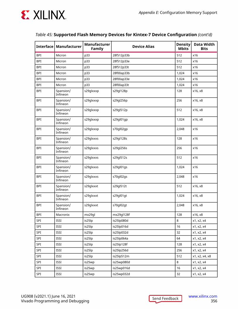
Table 45: Supported Flash Memory Devices for Kintex-7 Device Configuration (cont'd)
Interface Manufacturer ManufacturerFamily Device Alias Density
MbitsData Width
BitsBPI Micron p33 28f512p33b 512 x16
BPI Micron p33 28f512p33e 512 x16
BPI Micron p33 28f512p33t 512 x16
BPI Micron p33 28f00ap33b 1,024 x16
BPI Micron p33 28f00ap33e 1,024 x16
BPI Micron p33 28f00ap33t 1,024 x16
BPI Spansion/Infineon
s29glxxxp s29gl128p 128 x16, x8
BPI Spansion/Infineon
s29glxxxp s29gl256p 256 x16, x8
BPI Spansion/Infineon
s29glxxxp s29gl512p 512 x16, x8
BPI Spansion/Infineon
s29glxxxp s29gl01gp 1,024 x16, x8
BPI Spansion/Infineon
s29glxxxp s70gl02gp 2,048 x16
BPI Spansion/Infineon
s29glxxxs s29gl128s 128 x16
BPI Spansion/Infineon
s29glxxxs s29gl256s 256 x16
BPI Spansion/Infineon
s29glxxxs s29gl512s 512 x16
BPI Spansion/Infineon
s29glxxxs s29gl01gs 1,024 x16
BPI Spansion/Infineon
s29glxxxs s70gl02gs 2,048 x16
BPI Spansion/Infineon
s29glxxxt s29gl512t 512 x16, x8
BPI Spansion/Infineon
s29glxxxt s29gl01gt 1,024 x16, x8
BPI Spansion/Infineon
s29glxxxt s70gl02gt 2,048 x16, x8
BPI Macronix mx29gl mx29gl128f 128 x16, x8
SPI ISSI is25lp is25lp080d 8 x1, x2, x4
SPI ISSI is25lp is25lp016d 16 x1, x2, x4
SPI ISSI is25lp is25lp032d 32 x1, x2, x4
SPI ISSI is25lp is25lp064a 64 x1, x2, x4
SPI ISSI is25lp is25lp128f 128 x1, x2, x4
SPI ISSI is25lp is25lp256d 256 x1, x2, x4
SPI ISSI is25lp is25lp512m 512 x1, x2, x4, x8
SPI ISSI is25wp is25wp080d 8 x1, x2, x4
SPI ISSI is25wp is25wp016d 16 x1, x2, x4
SPI ISSI is25wp is25wp032d 32 x1, x2, x4
Appendix E: Configuration Memory Support
UG908 (v2021.1) June 16, 2021 www.xilinx.comVivado Programming and Debugging 356Send Feedback
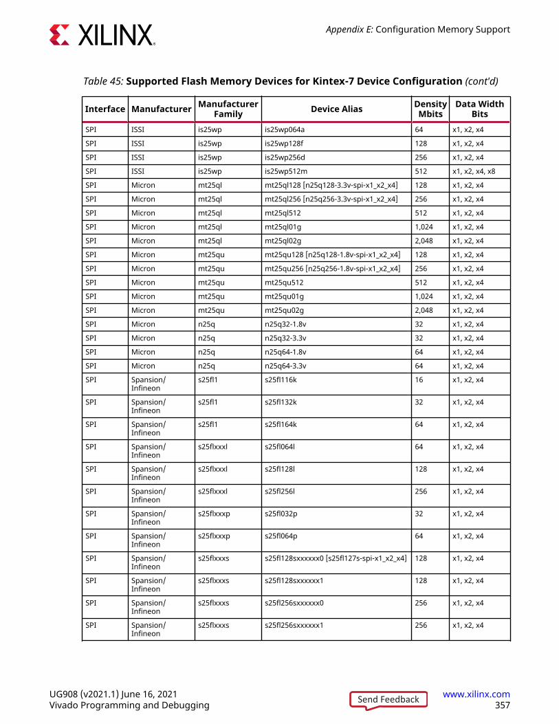
Table 45: Supported Flash Memory Devices for Kintex-7 Device Configuration (cont'd)
Interface Manufacturer ManufacturerFamily Device Alias Density
MbitsData Width
BitsSPI ISSI is25wp is25wp064a 64 x1, x2, x4
SPI ISSI is25wp is25wp128f 128 x1, x2, x4
SPI ISSI is25wp is25wp256d 256 x1, x2, x4
SPI ISSI is25wp is25wp512m 512 x1, x2, x4, x8
SPI Micron mt25ql mt25ql128 [n25q128-3.3v-spi-x1_x2_x4] 128 x1, x2, x4
SPI Micron mt25ql mt25ql256 [n25q256-3.3v-spi-x1_x2_x4] 256 x1, x2, x4
SPI Micron mt25ql mt25ql512 512 x1, x2, x4
SPI Micron mt25ql mt25ql01g 1,024 x1, x2, x4
SPI Micron mt25ql mt25ql02g 2,048 x1, x2, x4
SPI Micron mt25qu mt25qu128 [n25q128-1.8v-spi-x1_x2_x4] 128 x1, x2, x4
SPI Micron mt25qu mt25qu256 [n25q256-1.8v-spi-x1_x2_x4] 256 x1, x2, x4
SPI Micron mt25qu mt25qu512 512 x1, x2, x4
SPI Micron mt25qu mt25qu01g 1,024 x1, x2, x4
SPI Micron mt25qu mt25qu02g 2,048 x1, x2, x4
SPI Micron n25q n25q32-1.8v 32 x1, x2, x4
SPI Micron n25q n25q32-3.3v 32 x1, x2, x4
SPI Micron n25q n25q64-1.8v 64 x1, x2, x4
SPI Micron n25q n25q64-3.3v 64 x1, x2, x4
SPI Spansion/Infineon
s25fl1 s25fl116k 16 x1, x2, x4
SPI Spansion/Infineon
s25fl1 s25fl132k 32 x1, x2, x4
SPI Spansion/Infineon
s25fl1 s25fl164k 64 x1, x2, x4
SPI Spansion/Infineon
s25flxxxl s25fl064l 64 x1, x2, x4
SPI Spansion/Infineon
s25flxxxl s25fl128l 128 x1, x2, x4
SPI Spansion/Infineon
s25flxxxl s25fl256l 256 x1, x2, x4
SPI Spansion/Infineon
s25flxxxp s25fl032p 32 x1, x2, x4
SPI Spansion/Infineon
s25flxxxp s25fl064p 64 x1, x2, x4
SPI Spansion/Infineon
s25flxxxs s25fl128sxxxxxx0 [s25fl127s-spi-x1_x2_x4] 128 x1, x2, x4
SPI Spansion/Infineon
s25flxxxs s25fl128sxxxxxx1 128 x1, x2, x4
SPI Spansion/Infineon
s25flxxxs s25fl256sxxxxxx0 256 x1, x2, x4
SPI Spansion/Infineon
s25flxxxs s25fl256sxxxxxx1 256 x1, x2, x4
Appendix E: Configuration Memory Support
UG908 (v2021.1) June 16, 2021 www.xilinx.comVivado Programming and Debugging 357Send Feedback
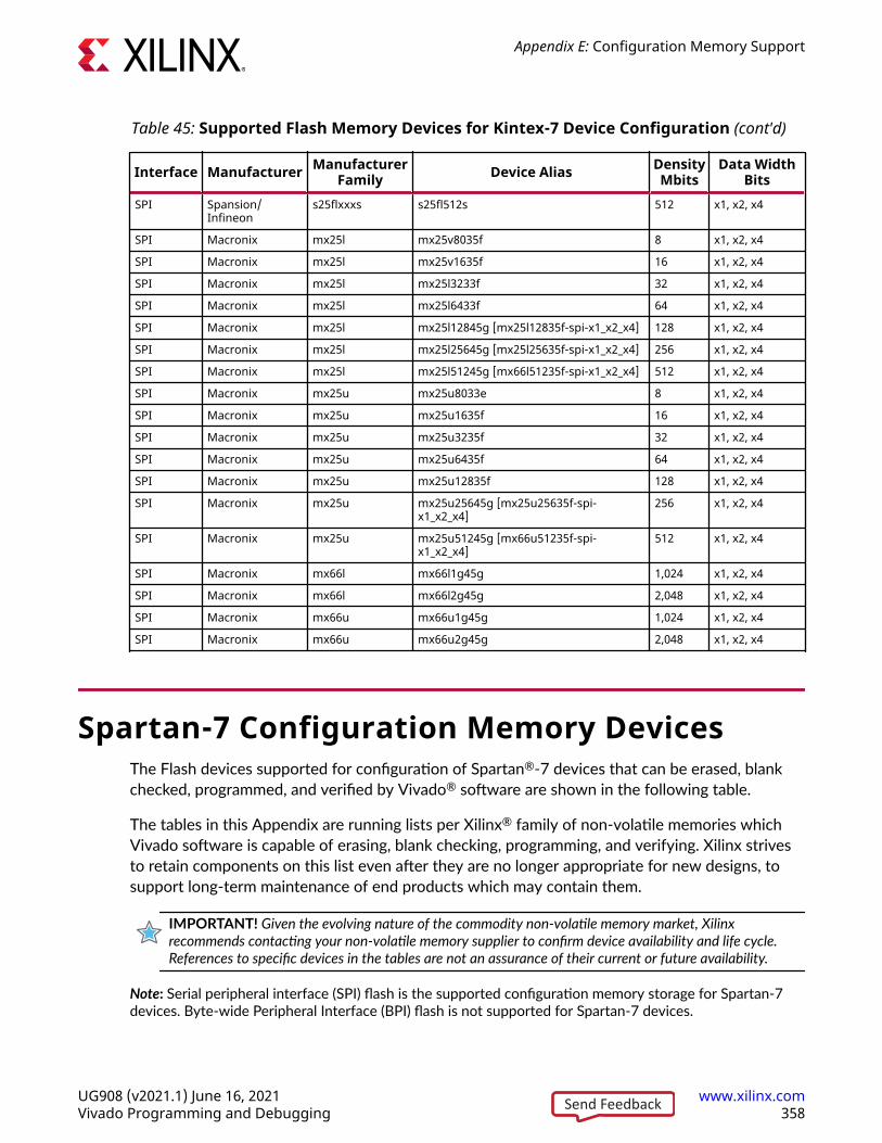
Table 45: Supported Flash Memory Devices for Kintex-7 Device Configuration (cont'd)
Interface Manufacturer ManufacturerFamily Device Alias Density
MbitsData Width
BitsSPI Spansion/
Infineons25flxxxs s25fl512s 512 x1, x2, x4
SPI Macronix mx25l mx25v8035f 8 x1, x2, x4
SPI Macronix mx25l mx25v1635f 16 x1, x2, x4
SPI Macronix mx25l mx25l3233f 32 x1, x2, x4
SPI Macronix mx25l mx25l6433f 64 x1, x2, x4
SPI Macronix mx25l mx25l12845g [mx25l12835f-spi-x1_x2_x4] 128 x1, x2, x4
SPI Macronix mx25l mx25l25645g [mx25l25635f-spi-x1_x2_x4] 256 x1, x2, x4
SPI Macronix mx25l mx25l51245g [mx66l51235f-spi-x1_x2_x4] 512 x1, x2, x4
SPI Macronix mx25u mx25u8033e 8 x1, x2, x4
SPI Macronix mx25u mx25u1635f 16 x1, x2, x4
SPI Macronix mx25u mx25u3235f 32 x1, x2, x4
SPI Macronix mx25u mx25u6435f 64 x1, x2, x4
SPI Macronix mx25u mx25u12835f 128 x1, x2, x4
SPI Macronix mx25u mx25u25645g [mx25u25635f-spi-x1_x2_x4]
256 x1, x2, x4
SPI Macronix mx25u mx25u51245g [mx66u51235f-spi-x1_x2_x4]
512 x1, x2, x4
SPI Macronix mx66l mx66l1g45g 1,024 x1, x2, x4
SPI Macronix mx66l mx66l2g45g 2,048 x1, x2, x4
SPI Macronix mx66u mx66u1g45g 1,024 x1, x2, x4
SPI Macronix mx66u mx66u2g45g 2,048 x1, x2, x4
Spartan-7 Configuration Memory DevicesThe Flash devices supported for configuration of Spartan®-7 devices that can be erased, blankchecked, programmed, and verified by Vivado® software are shown in the following table.
The tables in this Appendix are running lists per Xilinx® family of non-volatile memories whichVivado software is capable of erasing, blank checking, programming, and verifying. Xilinx strivesto retain components on this list even after they are no longer appropriate for new designs, tosupport long-term maintenance of end products which may contain them.
IMPORTANT! Given the evolving nature of the commodity non-volatile memory market, Xilinxrecommends contacting your non-volatile memory supplier to confirm device availability and life cycle.References to specific devices in the tables are not an assurance of their current or future availability.
Note: Serial peripheral interface (SPI) flash is the supported configuration memory storage for Spartan-7devices. Byte-wide Peripheral Interface (BPI) flash is not supported for Spartan-7 devices.
Appendix E: Configuration Memory Support
UG908 (v2021.1) June 16, 2021 www.xilinx.comVivado Programming and Debugging 358Send Feedback
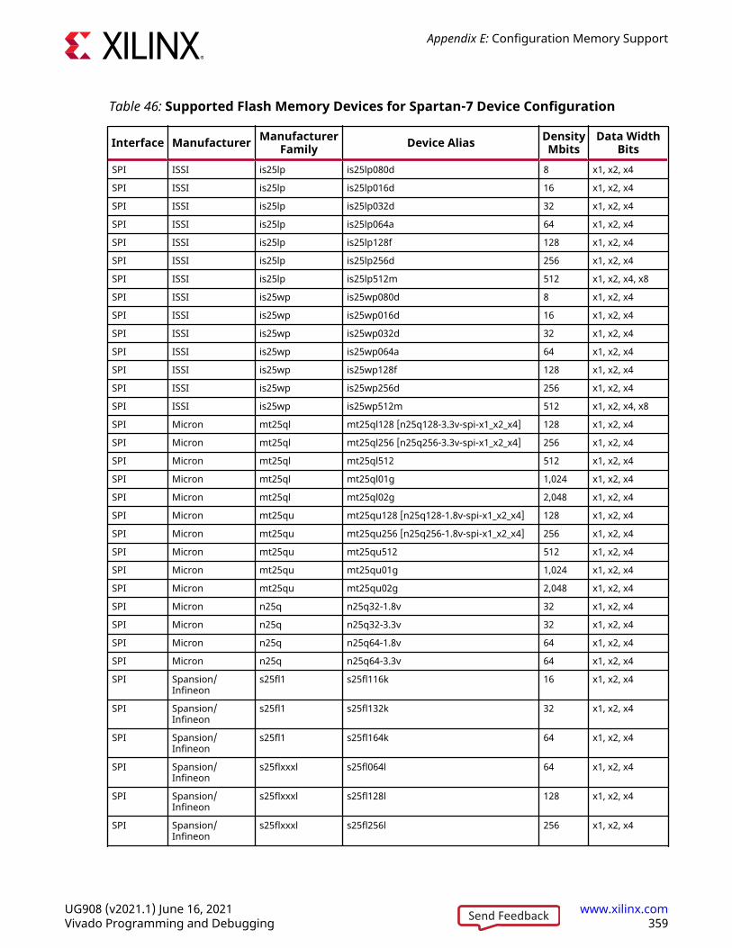
Table 46: Supported Flash Memory Devices for Spartan-7 Device Configuration
Interface Manufacturer ManufacturerFamily Device Alias Density
MbitsData Width
BitsSPI ISSI is25lp is25lp080d 8 x1, x2, x4
SPI ISSI is25lp is25lp016d 16 x1, x2, x4
SPI ISSI is25lp is25lp032d 32 x1, x2, x4
SPI ISSI is25lp is25lp064a 64 x1, x2, x4
SPI ISSI is25lp is25lp128f 128 x1, x2, x4
SPI ISSI is25lp is25lp256d 256 x1, x2, x4
SPI ISSI is25lp is25lp512m 512 x1, x2, x4, x8
SPI ISSI is25wp is25wp080d 8 x1, x2, x4
SPI ISSI is25wp is25wp016d 16 x1, x2, x4
SPI ISSI is25wp is25wp032d 32 x1, x2, x4
SPI ISSI is25wp is25wp064a 64 x1, x2, x4
SPI ISSI is25wp is25wp128f 128 x1, x2, x4
SPI ISSI is25wp is25wp256d 256 x1, x2, x4
SPI ISSI is25wp is25wp512m 512 x1, x2, x4, x8
SPI Micron mt25ql mt25ql128 [n25q128-3.3v-spi-x1_x2_x4] 128 x1, x2, x4
SPI Micron mt25ql mt25ql256 [n25q256-3.3v-spi-x1_x2_x4] 256 x1, x2, x4
SPI Micron mt25ql mt25ql512 512 x1, x2, x4
SPI Micron mt25ql mt25ql01g 1,024 x1, x2, x4
SPI Micron mt25ql mt25ql02g 2,048 x1, x2, x4
SPI Micron mt25qu mt25qu128 [n25q128-1.8v-spi-x1_x2_x4] 128 x1, x2, x4
SPI Micron mt25qu mt25qu256 [n25q256-1.8v-spi-x1_x2_x4] 256 x1, x2, x4
SPI Micron mt25qu mt25qu512 512 x1, x2, x4
SPI Micron mt25qu mt25qu01g 1,024 x1, x2, x4
SPI Micron mt25qu mt25qu02g 2,048 x1, x2, x4
SPI Micron n25q n25q32-1.8v 32 x1, x2, x4
SPI Micron n25q n25q32-3.3v 32 x1, x2, x4
SPI Micron n25q n25q64-1.8v 64 x1, x2, x4
SPI Micron n25q n25q64-3.3v 64 x1, x2, x4
SPI Spansion/Infineon
s25fl1 s25fl116k 16 x1, x2, x4
SPI Spansion/Infineon
s25fl1 s25fl132k 32 x1, x2, x4
SPI Spansion/Infineon
s25fl1 s25fl164k 64 x1, x2, x4
SPI Spansion/Infineon
s25flxxxl s25fl064l 64 x1, x2, x4
SPI Spansion/Infineon
s25flxxxl s25fl128l 128 x1, x2, x4
SPI Spansion/Infineon
s25flxxxl s25fl256l 256 x1, x2, x4
Appendix E: Configuration Memory Support
UG908 (v2021.1) June 16, 2021 www.xilinx.comVivado Programming and Debugging 359Send Feedback
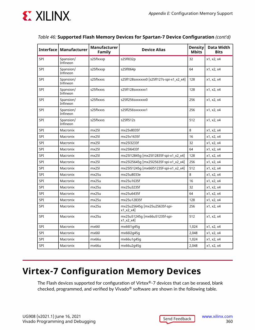
Table 46: Supported Flash Memory Devices for Spartan-7 Device Configuration (cont'd)
Interface Manufacturer ManufacturerFamily Device Alias Density
MbitsData Width
BitsSPI Spansion/
Infineons25flxxxp s25fl032p 32 x1, x2, x4
SPI Spansion/Infineon
s25flxxxp s25fl064p 64 x1, x2, x4
SPI Spansion/Infineon
s25flxxxs s25fl128sxxxxxx0 [s25fl127s-spi-x1_x2_x4] 128 x1, x2, x4
SPI Spansion/Infineon
s25flxxxs s25fl128sxxxxxx1 128 x1, x2, x4
SPI Spansion/Infineon
s25flxxxs s25fl256sxxxxxx0 256 x1, x2, x4
SPI Spansion/Infineon
s25flxxxs s25fl256sxxxxxx1 256 x1, x2, x4
SPI Spansion/Infineon
s25flxxxs s25fl512s 512 x1, x2, x4
SPI Macronix mx25l mx25v8035f 8 x1, x2, x4
SPI Macronix mx25l mx25v1635f 16 x1, x2, x4
SPI Macronix mx25l mx25l3233f 32 x1, x2, x4
SPI Macronix mx25l mx25l6433f 64 x1, x2, x4
SPI Macronix mx25l mx25l12845g [mx25l12835f-spi-x1_x2_x4] 128 x1, x2, x4
SPI Macronix mx25l mx25l25645g [mx25l25635f-spi-x1_x2_x4] 256 x1, x2, x4
SPI Macronix mx25l mx25l51245g [mx66l51235f-spi-x1_x2_x4] 512 x1, x2, x4
SPI Macronix mx25u mx25u8033e 8 x1, x2, x4
SPI Macronix mx25u mx25u1635f 16 x1, x2, x4
SPI Macronix mx25u mx25u3235f 32 x1, x2, x4
SPI Macronix mx25u mx25u6435f 64 x1, x2, x4
SPI Macronix mx25u mx25u12835f 128 x1, x2, x4
SPI Macronix mx25u mx25u25645g [mx25u25635f-spi-x1_x2_x4]
256 x1, x2, x4
SPI Macronix mx25u mx25u51245g [mx66u51235f-spi-x1_x2_x4]
512 x1, x2, x4
SPI Macronix mx66l mx66l1g45g 1,024 x1, x2, x4
SPI Macronix mx66l mx66l2g45g 2,048 x1, x2, x4
SPI Macronix mx66u mx66u1g45g 1,024 x1, x2, x4
SPI Macronix mx66u mx66u2g45g 2,048 x1, x2, x4
Virtex-7 Configuration Memory DevicesThe Flash devices supported for configuration of Virtex®-7 devices that can be erased, blankchecked, programmed, and verified by Vivado® software are shown in the following table.
Appendix E: Configuration Memory Support
UG908 (v2021.1) June 16, 2021 www.xilinx.comVivado Programming and Debugging 360Send Feedback
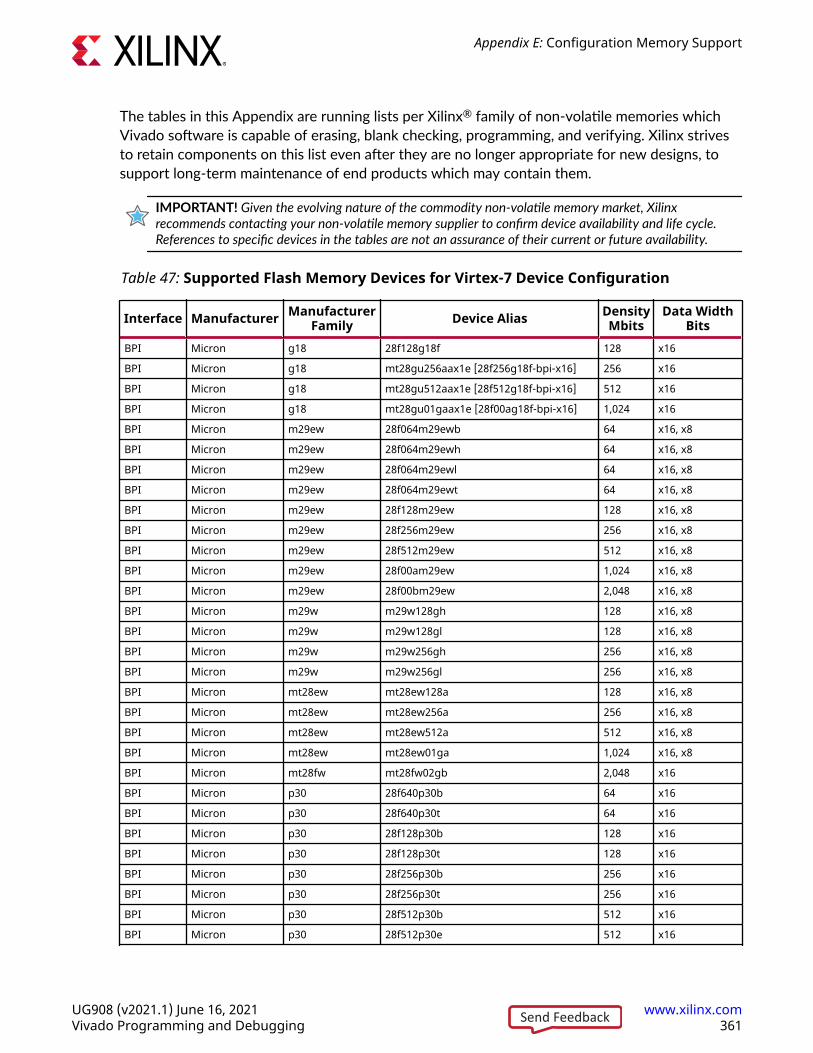
The tables in this Appendix are running lists per Xilinx® family of non-volatile memories whichVivado software is capable of erasing, blank checking, programming, and verifying. Xilinx strivesto retain components on this list even after they are no longer appropriate for new designs, tosupport long-term maintenance of end products which may contain them.
IMPORTANT! Given the evolving nature of the commodity non-volatile memory market, Xilinxrecommends contacting your non-volatile memory supplier to confirm device availability and life cycle.References to specific devices in the tables are not an assurance of their current or future availability.
Table 47: Supported Flash Memory Devices for Virtex-7 Device Configuration
Interface Manufacturer ManufacturerFamily Device Alias Density
MbitsData Width
BitsBPI Micron g18 28f128g18f 128 x16
BPI Micron g18 mt28gu256aax1e [28f256g18f-bpi-x16] 256 x16
BPI Micron g18 mt28gu512aax1e [28f512g18f-bpi-x16] 512 x16
BPI Micron g18 mt28gu01gaax1e [28f00ag18f-bpi-x16] 1,024 x16
BPI Micron m29ew 28f064m29ewb 64 x16, x8
BPI Micron m29ew 28f064m29ewh 64 x16, x8
BPI Micron m29ew 28f064m29ewl 64 x16, x8
BPI Micron m29ew 28f064m29ewt 64 x16, x8
BPI Micron m29ew 28f128m29ew 128 x16, x8
BPI Micron m29ew 28f256m29ew 256 x16, x8
BPI Micron m29ew 28f512m29ew 512 x16, x8
BPI Micron m29ew 28f00am29ew 1,024 x16, x8
BPI Micron m29ew 28f00bm29ew 2,048 x16, x8
BPI Micron m29w m29w128gh 128 x16, x8
BPI Micron m29w m29w128gl 128 x16, x8
BPI Micron m29w m29w256gh 256 x16, x8
BPI Micron m29w m29w256gl 256 x16, x8
BPI Micron mt28ew mt28ew128a 128 x16, x8
BPI Micron mt28ew mt28ew256a 256 x16, x8
BPI Micron mt28ew mt28ew512a 512 x16, x8
BPI Micron mt28ew mt28ew01ga 1,024 x16, x8
BPI Micron mt28fw mt28fw02gb 2,048 x16
BPI Micron p30 28f640p30b 64 x16
BPI Micron p30 28f640p30t 64 x16
BPI Micron p30 28f128p30b 128 x16
BPI Micron p30 28f128p30t 128 x16
BPI Micron p30 28f256p30b 256 x16
BPI Micron p30 28f256p30t 256 x16
BPI Micron p30 28f512p30b 512 x16
BPI Micron p30 28f512p30e 512 x16
Appendix E: Configuration Memory Support
UG908 (v2021.1) June 16, 2021 www.xilinx.comVivado Programming and Debugging 361Send Feedback
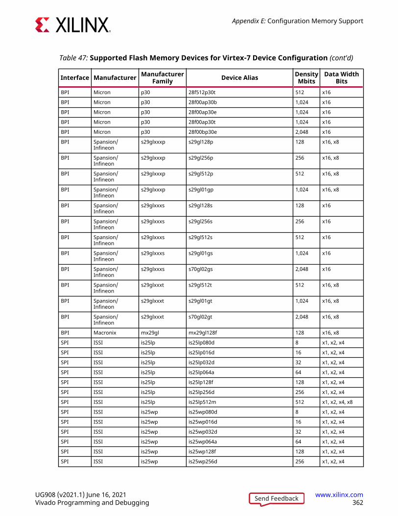
Table 47: Supported Flash Memory Devices for Virtex-7 Device Configuration (cont'd)
Interface Manufacturer ManufacturerFamily Device Alias Density
MbitsData Width
BitsBPI Micron p30 28f512p30t 512 x16
BPI Micron p30 28f00ap30b 1,024 x16
BPI Micron p30 28f00ap30e 1,024 x16
BPI Micron p30 28f00ap30t 1,024 x16
BPI Micron p30 28f00bp30e 2,048 x16
BPI Spansion/Infineon
s29glxxxp s29gl128p 128 x16, x8
BPI Spansion/Infineon
s29glxxxp s29gl256p 256 x16, x8
BPI Spansion/Infineon
s29glxxxp s29gl512p 512 x16, x8
BPI Spansion/Infineon
s29glxxxp s29gl01gp 1,024 x16, x8
BPI Spansion/Infineon
s29glxxxs s29gl128s 128 x16
BPI Spansion/Infineon
s29glxxxs s29gl256s 256 x16
BPI Spansion/Infineon
s29glxxxs s29gl512s 512 x16
BPI Spansion/Infineon
s29glxxxs s29gl01gs 1,024 x16
BPI Spansion/Infineon
s29glxxxs s70gl02gs 2,048 x16
BPI Spansion/Infineon
s29glxxxt s29gl512t 512 x16, x8
BPI Spansion/Infineon
s29glxxxt s29gl01gt 1,024 x16, x8
BPI Spansion/Infineon
s29glxxxt s70gl02gt 2,048 x16, x8
BPI Macronix mx29gl mx29gl128f 128 x16, x8
SPI ISSI is25lp is25lp080d 8 x1, x2, x4
SPI ISSI is25lp is25lp016d 16 x1, x2, x4
SPI ISSI is25lp is25lp032d 32 x1, x2, x4
SPI ISSI is25lp is25lp064a 64 x1, x2, x4
SPI ISSI is25lp is25lp128f 128 x1, x2, x4
SPI ISSI is25lp is25lp256d 256 x1, x2, x4
SPI ISSI is25lp is25lp512m 512 x1, x2, x4, x8
SPI ISSI is25wp is25wp080d 8 x1, x2, x4
SPI ISSI is25wp is25wp016d 16 x1, x2, x4
SPI ISSI is25wp is25wp032d 32 x1, x2, x4
SPI ISSI is25wp is25wp064a 64 x1, x2, x4
SPI ISSI is25wp is25wp128f 128 x1, x2, x4
SPI ISSI is25wp is25wp256d 256 x1, x2, x4
Appendix E: Configuration Memory Support
UG908 (v2021.1) June 16, 2021 www.xilinx.comVivado Programming and Debugging 362Send Feedback
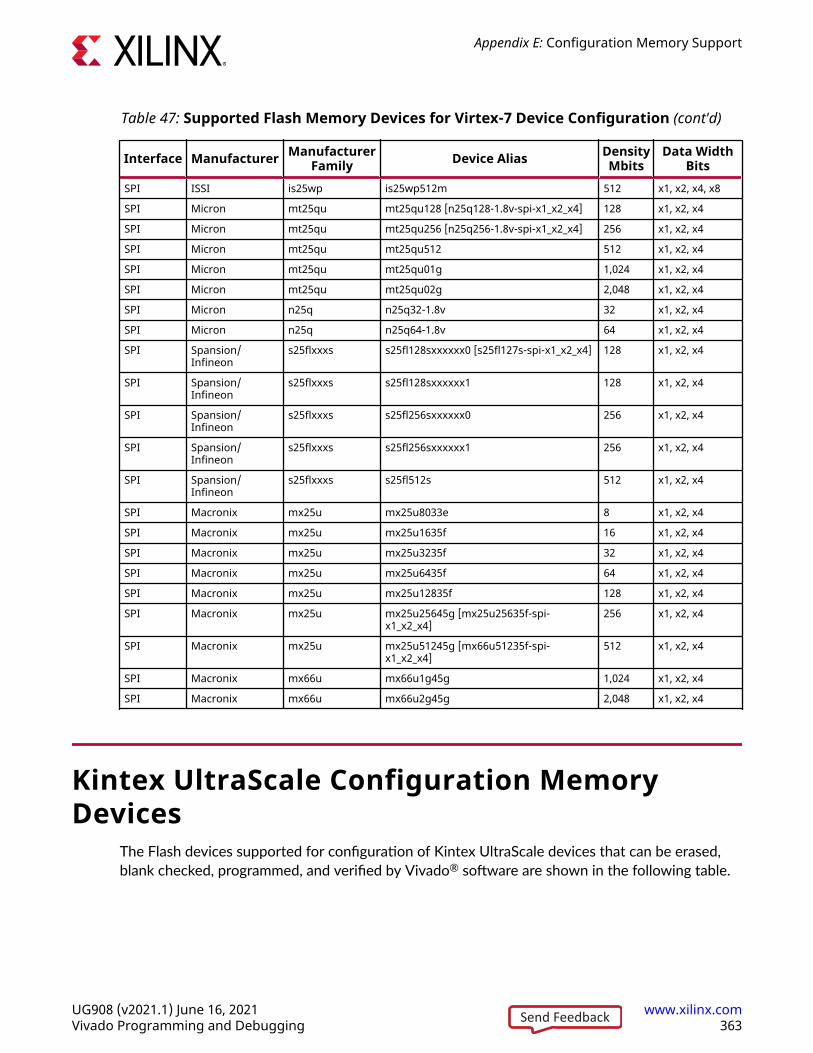
Table 47: Supported Flash Memory Devices for Virtex-7 Device Configuration (cont'd)
Interface Manufacturer ManufacturerFamily Device Alias Density
MbitsData Width
BitsSPI ISSI is25wp is25wp512m 512 x1, x2, x4, x8
SPI Micron mt25qu mt25qu128 [n25q128-1.8v-spi-x1_x2_x4] 128 x1, x2, x4
SPI Micron mt25qu mt25qu256 [n25q256-1.8v-spi-x1_x2_x4] 256 x1, x2, x4
SPI Micron mt25qu mt25qu512 512 x1, x2, x4
SPI Micron mt25qu mt25qu01g 1,024 x1, x2, x4
SPI Micron mt25qu mt25qu02g 2,048 x1, x2, x4
SPI Micron n25q n25q32-1.8v 32 x1, x2, x4
SPI Micron n25q n25q64-1.8v 64 x1, x2, x4
SPI Spansion/Infineon
s25flxxxs s25fl128sxxxxxx0 [s25fl127s-spi-x1_x2_x4] 128 x1, x2, x4
SPI Spansion/Infineon
s25flxxxs s25fl128sxxxxxx1 128 x1, x2, x4
SPI Spansion/Infineon
s25flxxxs s25fl256sxxxxxx0 256 x1, x2, x4
SPI Spansion/Infineon
s25flxxxs s25fl256sxxxxxx1 256 x1, x2, x4
SPI Spansion/Infineon
s25flxxxs s25fl512s 512 x1, x2, x4
SPI Macronix mx25u mx25u8033e 8 x1, x2, x4
SPI Macronix mx25u mx25u1635f 16 x1, x2, x4
SPI Macronix mx25u mx25u3235f 32 x1, x2, x4
SPI Macronix mx25u mx25u6435f 64 x1, x2, x4
SPI Macronix mx25u mx25u12835f 128 x1, x2, x4
SPI Macronix mx25u mx25u25645g [mx25u25635f-spi-x1_x2_x4]
256 x1, x2, x4
SPI Macronix mx25u mx25u51245g [mx66u51235f-spi-x1_x2_x4]
512 x1, x2, x4
SPI Macronix mx66u mx66u1g45g 1,024 x1, x2, x4
SPI Macronix mx66u mx66u2g45g 2,048 x1, x2, x4
Kintex UltraScale Configuration MemoryDevices
The Flash devices supported for configuration of Kintex UltraScale devices that can be erased,blank checked, programmed, and verified by Vivado® software are shown in the following table.
Appendix E: Configuration Memory Support
UG908 (v2021.1) June 16, 2021 www.xilinx.comVivado Programming and Debugging 363Send Feedback
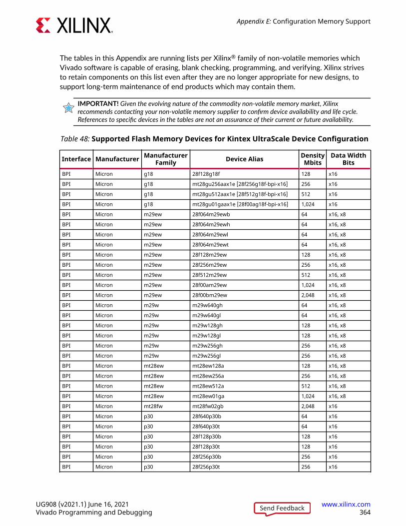
The tables in this Appendix are running lists per Xilinx® family of non-volatile memories whichVivado software is capable of erasing, blank checking, programming, and verifying. Xilinx strivesto retain components on this list even after they are no longer appropriate for new designs, tosupport long-term maintenance of end products which may contain them.
IMPORTANT! Given the evolving nature of the commodity non-volatile memory market, Xilinxrecommends contacting your non-volatile memory supplier to confirm device availability and life cycle.References to specific devices in the tables are not an assurance of their current or future availability.
Table 48: Supported Flash Memory Devices for Kintex UltraScale Device Configuration
Interface Manufacturer ManufacturerFamily Device Alias Density
MbitsData Width
BitsBPI Micron g18 28f128g18f 128 x16
BPI Micron g18 mt28gu256aax1e [28f256g18f-bpi-x16] 256 x16
BPI Micron g18 mt28gu512aax1e [28f512g18f-bpi-x16] 512 x16
BPI Micron g18 mt28gu01gaax1e [28f00ag18f-bpi-x16] 1,024 x16
BPI Micron m29ew 28f064m29ewb 64 x16, x8
BPI Micron m29ew 28f064m29ewh 64 x16, x8
BPI Micron m29ew 28f064m29ewl 64 x16, x8
BPI Micron m29ew 28f064m29ewt 64 x16, x8
BPI Micron m29ew 28f128m29ew 128 x16, x8
BPI Micron m29ew 28f256m29ew 256 x16, x8
BPI Micron m29ew 28f512m29ew 512 x16, x8
BPI Micron m29ew 28f00am29ew 1,024 x16, x8
BPI Micron m29ew 28f00bm29ew 2,048 x16, x8
BPI Micron m29w m29w640gh 64 x16, x8
BPI Micron m29w m29w640gl 64 x16, x8
BPI Micron m29w m29w128gh 128 x16, x8
BPI Micron m29w m29w128gl 128 x16, x8
BPI Micron m29w m29w256gh 256 x16, x8
BPI Micron m29w m29w256gl 256 x16, x8
BPI Micron mt28ew mt28ew128a 128 x16, x8
BPI Micron mt28ew mt28ew256a 256 x16, x8
BPI Micron mt28ew mt28ew512a 512 x16, x8
BPI Micron mt28ew mt28ew01ga 1,024 x16, x8
BPI Micron mt28fw mt28fw02gb 2,048 x16
BPI Micron p30 28f640p30b 64 x16
BPI Micron p30 28f640p30t 64 x16
BPI Micron p30 28f128p30b 128 x16
BPI Micron p30 28f128p30t 128 x16
BPI Micron p30 28f256p30b 256 x16
BPI Micron p30 28f256p30t 256 x16
Appendix E: Configuration Memory Support
UG908 (v2021.1) June 16, 2021 www.xilinx.comVivado Programming and Debugging 364Send Feedback
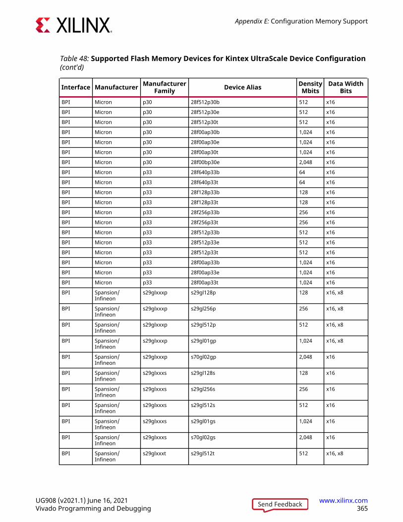
Table 48: Supported Flash Memory Devices for Kintex UltraScale Device Configuration(cont'd)
Interface Manufacturer ManufacturerFamily Device Alias Density
MbitsData Width
BitsBPI Micron p30 28f512p30b 512 x16
BPI Micron p30 28f512p30e 512 x16
BPI Micron p30 28f512p30t 512 x16
BPI Micron p30 28f00ap30b 1,024 x16
BPI Micron p30 28f00ap30e 1,024 x16
BPI Micron p30 28f00ap30t 1,024 x16
BPI Micron p30 28f00bp30e 2,048 x16
BPI Micron p33 28f640p33b 64 x16
BPI Micron p33 28f640p33t 64 x16
BPI Micron p33 28f128p33b 128 x16
BPI Micron p33 28f128p33t 128 x16
BPI Micron p33 28f256p33b 256 x16
BPI Micron p33 28f256p33t 256 x16
BPI Micron p33 28f512p33b 512 x16
BPI Micron p33 28f512p33e 512 x16
BPI Micron p33 28f512p33t 512 x16
BPI Micron p33 28f00ap33b 1,024 x16
BPI Micron p33 28f00ap33e 1,024 x16
BPI Micron p33 28f00ap33t 1,024 x16
BPI Spansion/Infineon
s29glxxxp s29gl128p 128 x16, x8
BPI Spansion/Infineon
s29glxxxp s29gl256p 256 x16, x8
BPI Spansion/Infineon
s29glxxxp s29gl512p 512 x16, x8
BPI Spansion/Infineon
s29glxxxp s29gl01gp 1,024 x16, x8
BPI Spansion/Infineon
s29glxxxp s70gl02gp 2,048 x16
BPI Spansion/Infineon
s29glxxxs s29gl128s 128 x16
BPI Spansion/Infineon
s29glxxxs s29gl256s 256 x16
BPI Spansion/Infineon
s29glxxxs s29gl512s 512 x16
BPI Spansion/Infineon
s29glxxxs s29gl01gs 1,024 x16
BPI Spansion/Infineon
s29glxxxs s70gl02gs 2,048 x16
BPI Spansion/Infineon
s29glxxxt s29gl512t 512 x16, x8
Appendix E: Configuration Memory Support
UG908 (v2021.1) June 16, 2021 www.xilinx.comVivado Programming and Debugging 365Send Feedback
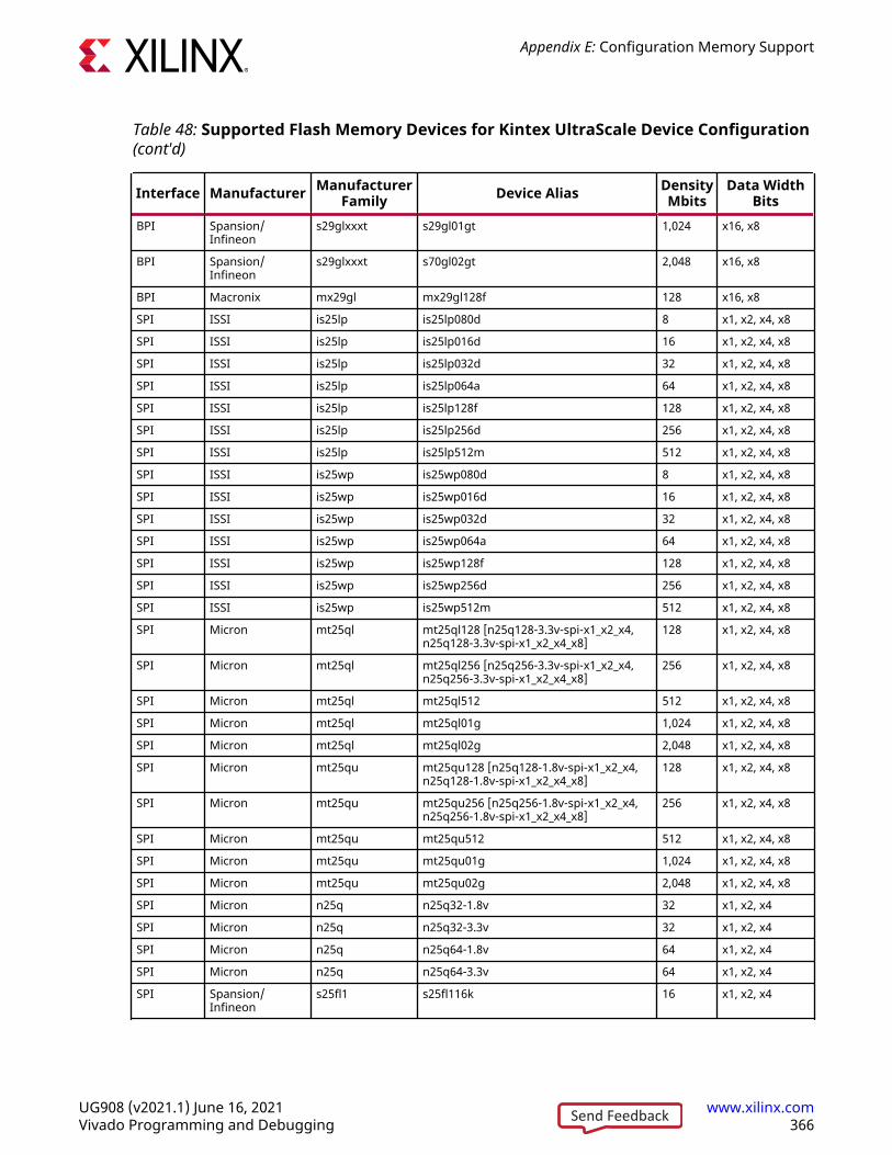
Table 48: Supported Flash Memory Devices for Kintex UltraScale Device Configuration(cont'd)
Interface Manufacturer ManufacturerFamily Device Alias Density
MbitsData Width
BitsBPI Spansion/
Infineons29glxxxt s29gl01gt 1,024 x16, x8
BPI Spansion/Infineon
s29glxxxt s70gl02gt 2,048 x16, x8
BPI Macronix mx29gl mx29gl128f 128 x16, x8
SPI ISSI is25lp is25lp080d 8 x1, x2, x4, x8
SPI ISSI is25lp is25lp016d 16 x1, x2, x4, x8
SPI ISSI is25lp is25lp032d 32 x1, x2, x4, x8
SPI ISSI is25lp is25lp064a 64 x1, x2, x4, x8
SPI ISSI is25lp is25lp128f 128 x1, x2, x4, x8
SPI ISSI is25lp is25lp256d 256 x1, x2, x4, x8
SPI ISSI is25lp is25lp512m 512 x1, x2, x4, x8
SPI ISSI is25wp is25wp080d 8 x1, x2, x4, x8
SPI ISSI is25wp is25wp016d 16 x1, x2, x4, x8
SPI ISSI is25wp is25wp032d 32 x1, x2, x4, x8
SPI ISSI is25wp is25wp064a 64 x1, x2, x4, x8
SPI ISSI is25wp is25wp128f 128 x1, x2, x4, x8
SPI ISSI is25wp is25wp256d 256 x1, x2, x4, x8
SPI ISSI is25wp is25wp512m 512 x1, x2, x4, x8
SPI Micron mt25ql mt25ql128 [n25q128-3.3v-spi-x1_x2_x4,n25q128-3.3v-spi-x1_x2_x4_x8]
128 x1, x2, x4, x8
SPI Micron mt25ql mt25ql256 [n25q256-3.3v-spi-x1_x2_x4,n25q256-3.3v-spi-x1_x2_x4_x8]
256 x1, x2, x4, x8
SPI Micron mt25ql mt25ql512 512 x1, x2, x4, x8
SPI Micron mt25ql mt25ql01g 1,024 x1, x2, x4, x8
SPI Micron mt25ql mt25ql02g 2,048 x1, x2, x4, x8
SPI Micron mt25qu mt25qu128 [n25q128-1.8v-spi-x1_x2_x4,n25q128-1.8v-spi-x1_x2_x4_x8]
128 x1, x2, x4, x8
SPI Micron mt25qu mt25qu256 [n25q256-1.8v-spi-x1_x2_x4,n25q256-1.8v-spi-x1_x2_x4_x8]
256 x1, x2, x4, x8
SPI Micron mt25qu mt25qu512 512 x1, x2, x4, x8
SPI Micron mt25qu mt25qu01g 1,024 x1, x2, x4, x8
SPI Micron mt25qu mt25qu02g 2,048 x1, x2, x4, x8
SPI Micron n25q n25q32-1.8v 32 x1, x2, x4
SPI Micron n25q n25q32-3.3v 32 x1, x2, x4
SPI Micron n25q n25q64-1.8v 64 x1, x2, x4
SPI Micron n25q n25q64-3.3v 64 x1, x2, x4
SPI Spansion/Infineon
s25fl1 s25fl116k 16 x1, x2, x4
Appendix E: Configuration Memory Support
UG908 (v2021.1) June 16, 2021 www.xilinx.comVivado Programming and Debugging 366Send Feedback
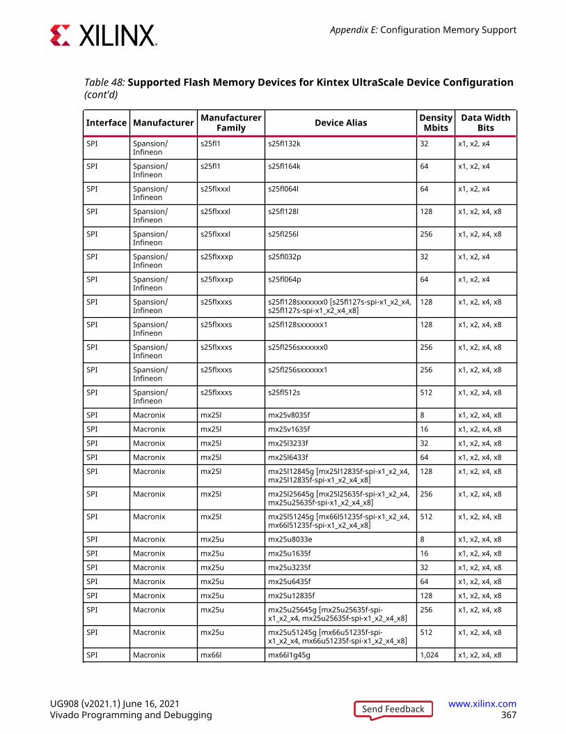
Table 48: Supported Flash Memory Devices for Kintex UltraScale Device Configuration(cont'd)
Interface Manufacturer ManufacturerFamily Device Alias Density
MbitsData Width
BitsSPI Spansion/
Infineons25fl1 s25fl132k 32 x1, x2, x4
SPI Spansion/Infineon
s25fl1 s25fl164k 64 x1, x2, x4
SPI Spansion/Infineon
s25flxxxl s25fl064l 64 x1, x2, x4
SPI Spansion/Infineon
s25flxxxl s25fl128l 128 x1, x2, x4, x8
SPI Spansion/Infineon
s25flxxxl s25fl256l 256 x1, x2, x4, x8
SPI Spansion/Infineon
s25flxxxp s25fl032p 32 x1, x2, x4
SPI Spansion/Infineon
s25flxxxp s25fl064p 64 x1, x2, x4
SPI Spansion/Infineon
s25flxxxs s25fl128sxxxxxx0 [s25fl127s-spi-x1_x2_x4,s25fl127s-spi-x1_x2_x4_x8]
128 x1, x2, x4, x8
SPI Spansion/Infineon
s25flxxxs s25fl128sxxxxxx1 128 x1, x2, x4, x8
SPI Spansion/Infineon
s25flxxxs s25fl256sxxxxxx0 256 x1, x2, x4, x8
SPI Spansion/Infineon
s25flxxxs s25fl256sxxxxxx1 256 x1, x2, x4, x8
SPI Spansion/Infineon
s25flxxxs s25fl512s 512 x1, x2, x4, x8
SPI Macronix mx25l mx25v8035f 8 x1, x2, x4, x8
SPI Macronix mx25l mx25v1635f 16 x1, x2, x4, x8
SPI Macronix mx25l mx25l3233f 32 x1, x2, x4, x8
SPI Macronix mx25l mx25l6433f 64 x1, x2, x4, x8
SPI Macronix mx25l mx25l12845g [mx25l12835f-spi-x1_x2_x4,mx25l12835f-spi-x1_x2_x4_x8]
128 x1, x2, x4, x8
SPI Macronix mx25l mx25l25645g [mx25l25635f-spi-x1_x2_x4,mx25u25635f-spi-x1_x2_x4_x8]
256 x1, x2, x4, x8
SPI Macronix mx25l mx25l51245g [mx66l51235f-spi-x1_x2_x4,mx66l51235f-spi-x1_x2_x4_x8]
512 x1, x2, x4, x8
SPI Macronix mx25u mx25u8033e 8 x1, x2, x4, x8
SPI Macronix mx25u mx25u1635f 16 x1, x2, x4, x8
SPI Macronix mx25u mx25u3235f 32 x1, x2, x4, x8
SPI Macronix mx25u mx25u6435f 64 x1, x2, x4, x8
SPI Macronix mx25u mx25u12835f 128 x1, x2, x4, x8
SPI Macronix mx25u mx25u25645g [mx25u25635f-spi-x1_x2_x4, mx25u25635f-spi-x1_x2_x4_x8]
256 x1, x2, x4, x8
SPI Macronix mx25u mx25u51245g [mx66u51235f-spi-x1_x2_x4, mx66u51235f-spi-x1_x2_x4_x8]
512 x1, x2, x4, x8
SPI Macronix mx66l mx66l1g45g 1,024 x1, x2, x4, x8
Appendix E: Configuration Memory Support
UG908 (v2021.1) June 16, 2021 www.xilinx.comVivado Programming and Debugging 367Send Feedback

Table 48: Supported Flash Memory Devices for Kintex UltraScale Device Configuration(cont'd)
Interface Manufacturer ManufacturerFamily Device Alias Density
MbitsData Width
BitsSPI Macronix mx66l mx66l2g45g 2,048 x1, x2, x4, x8
SPI Macronix mx66u mx66u1g45g 1,024 x1, x2, x4, x8
SPI Macronix mx66u mx66u2g45g 2,048 x1, x2, x4, x8
Kintex UltraScale+ Configuration MemoryDevices
The Flash devices supported for configuration of Kintex UltraScale+ devices that can be erased,blank checked, programmed, and verified by Vivado® software are shown in the following table.
The tables in this Appendix are running lists per Xilinx® family of non-volatile memories whichVivado software is capable of erasing, blank checking, programming, and verifying. Xilinx strivesto retain components on this list even after they are no longer appropriate for new designs, tosupport long-term maintenance of end products which may contain them.
IMPORTANT! Given the evolving nature of the commodity non-volatile memory market, Xilinxrecommends contacting your non-volatile memory supplier to confirm device availability and life cycle.References to specific devices in the tables are not an assurance of their current or future availability.
Table 49: Supported Flash Memory Devices for Kintex UltraScale+ DeviceConfiguration
Interface Manufacturer ManufacturerFamily Device Alias Density
MbitsData Width
BitsBPI Micron g18 28f128g18f 128 x16
BPI Micron g18 mt28gu256aax1e [28f256g18f-bpi-x16] 256 x16
BPI Micron g18 mt28gu512aax1e [28f512g18f-bpi-x16] 512 x16
BPI Micron g18 mt28gu01gaax1e [28f00ag18f-bpi-x16] 1,024 x16
BPI Micron m29ew 28f064m29ewb 64 x16, x8
BPI Micron m29ew 28f064m29ewh 64 x16, x8
BPI Micron m29ew 28f064m29ewl 64 x16, x8
BPI Micron m29ew 28f064m29ewt 64 x16, x8
BPI Micron m29ew 28f128m29ew 128 x16, x8
BPI Micron m29ew 28f256m29ew 256 x16, x8
BPI Micron m29ew 28f512m29ew 512 x16, x8
BPI Micron m29ew 28f00am29ew 1,024 x16, x8
Appendix E: Configuration Memory Support
UG908 (v2021.1) June 16, 2021 www.xilinx.comVivado Programming and Debugging 368Send Feedback
Table 49: Supported Flash Memory Devices for Kintex UltraScale+ DeviceConfiguration (cont'd)
Interface Manufacturer ManufacturerFamily Device Alias Density
MbitsData Width
BitsBPI Micron m29ew 28f00bm29ew 2,048 x16, x8
BPI Micron m29w m29w128gh 128 x16, x8
BPI Micron m29w m29w128gl 128 x16, x8
BPI Micron m29w m29w256gh 256 x16, x8
BPI Micron m29w m29w256gl 256 x16, x8
BPI Micron mt28ew mt28ew128a 128 x16, x8
BPI Micron mt28ew mt28ew256a 256 x16, x8
BPI Micron mt28ew mt28ew512a 512 x16, x8
BPI Micron mt28ew mt28ew01ga 1,024 x16, x8
BPI Micron mt28fw mt28fw02gb 2,048 x16
BPI Micron p30 28f640p30b 64 x16
BPI Micron p30 28f640p30t 64 x16
BPI Micron p30 28f128p30b 128 x16
BPI Micron p30 28f128p30t 128 x16
BPI Micron p30 28f256p30b 256 x16
BPI Micron p30 28f256p30t 256 x16
BPI Micron p30 28f512p30b 512 x16
BPI Micron p30 28f512p30e 512 x16
BPI Micron p30 28f512p30t 512 x16
BPI Micron p30 28f00ap30b 1,024 x16
BPI Micron p30 28f00ap30e 1,024 x16
BPI Micron p30 28f00ap30t 1,024 x16
BPI Micron p30 28f00bp30e 2,048 x16
BPI Spansion/Infineon
s29glxxxp s29gl128p 128 x16, x8
BPI Spansion/Infineon
s29glxxxp s29gl256p 256 x16, x8
BPI Spansion/Infineon
s29glxxxp s29gl512p 512 x16, x8
BPI Spansion/Infineon
s29glxxxp s29gl01gp 1,024 x16, x8
BPI Spansion/Infineon
s29glxxxs s29gl128s 128 x16
BPI Spansion/Infineon
s29glxxxs s29gl256s 256 x16
BPI Spansion/Infineon
s29glxxxs s29gl512s 512 x16
BPI Spansion/Infineon
s29glxxxs s29gl01gs 1,024 x16
BPI Spansion/Infineon
s29glxxxs s70gl02gs 2,048 x16
Appendix E: Configuration Memory Support
UG908 (v2021.1) June 16, 2021 www.xilinx.comVivado Programming and Debugging 369Send Feedback
Table 49: Supported Flash Memory Devices for Kintex UltraScale+ DeviceConfiguration (cont'd)
Interface Manufacturer ManufacturerFamily Device Alias Density
MbitsData Width
BitsBPI Spansion/
Infineons29glxxxt s29gl512t 512 x16, x8
BPI Spansion/Infineon
s29glxxxt s29gl01gt 1,024 x16, x8
BPI Spansion/Infineon
s29glxxxt s70gl02gt 2,048 x16, x8
BPI Macronix mx29gl mx29gl128f 128 x16, x8
SPI ISSI is25wp is25wp080d 8 x1, x2, x4, x8
SPI ISSI is25wp is25wp016d 16 x1, x2, x4, x8
SPI ISSI is25wp is25wp032d 32 x1, x2, x4, x8
SPI ISSI is25wp is25wp064a 64 x1, x2, x4, x8
SPI ISSI is25wp is25wp128f 128 x1, x2, x4, x8
SPI ISSI is25wp is25wp256d 256 x1, x2, x4, x8
SPI ISSI is25wp is25wp512m 512 x1, x2, x4, x8
SPI Micron mt25qu mt25qu128 [n25q128-1.8v-spi-x1_x2_x4,n25q128-1.8v-spi-x1_x2_x4_x8]
128 x1, x2, x4, x8
SPI Micron mt25qu mt25qu256 [n25q256-1.8v-spi-x1_x2_x4,n25q256-1.8v-spi-x1_x2_x4_x8]
256 x1, x2, x4, x8
SPI Micron mt25qu mt25qu512 512 x1, x2, x4, x8
SPI Micron mt25qu mt25qu01g 1,024 x1, x2, x4, x8
SPI Micron mt25qu mt25qu02g 2,048 x1, x2, x4, x8
SPI Micron n25q n25q32-1.8v 32 x1, x2, x4
SPI Micron n25q n25q64-1.8v 64 x1, x2, x4
SPI Spansion/Infineon
s25fl1 s25fl116k 16 x1, x2, x4
SPI Spansion/Infineon
s25fl1 s25fl132k 32 x1, x2, x4
SPI Spansion/Infineon
s25fl1 s25fl164k 64 x1, x2, x4
SPI Spansion/Infineon
s25flxxxl s25fl064l 64 x1, x2, x4
SPI Spansion/Infineon
s25flxxxl s25fl128l 128 x1, x2, x4, x8
SPI Spansion/Infineon
s25flxxxl s25fl256l 256 x1, x2, x4, x8
SPI Spansion/Infineon
s25flxxxp s25fl032p 32 x1, x2, x4
SPI Spansion/Infineon
s25flxxxp s25fl064p 64 x1, x2, x4
SPI Spansion/Infineon
s25flxxxs s25fl128sxxxxxx0 [s25fl127s-spi-x1_x2_x4,s25fl127s-spi-x1_x2_x4_x8]
128 x1, x2, x4, x8
SPI Spansion/Infineon
s25flxxxs s25fl128sxxxxxx1 128 x1, x2, x4, x8
Appendix E: Configuration Memory Support
UG908 (v2021.1) June 16, 2021 www.xilinx.comVivado Programming and Debugging 370Send Feedback

Table 49: Supported Flash Memory Devices for Kintex UltraScale+ DeviceConfiguration (cont'd)
Interface Manufacturer ManufacturerFamily Device Alias Density
MbitsData Width
BitsSPI Spansion/
Infineons25flxxxs s25fl256sxxxxxx0 256 x1, x2, x4, x8
SPI Spansion/Infineon
s25flxxxs s25fl256sxxxxxx1 256 x1, x2, x4, x8
SPI Spansion/Infineon
s25flxxxs s25fl512s 512 x1, x2, x4, x8
SPI Macronix mx25u mx25u8033e 8 x1, x2, x4, x8
SPI Macronix mx25u mx25u1635f 16 x1, x2, x4, x8
SPI Macronix mx25u mx25u3235f 32 x1, x2, x4, x8
SPI Macronix mx25u mx25u6435f 64 x1, x2, x4, x8
SPI Macronix mx25u mx25u12835f 128 x1, x2, x4, x8
SPI Macronix mx25u mx25u25645g [mx25u25635f-spi-x1_x2_x4, mx25u25635f-spi-x1_x2_x4_x8]
256 x1, x2, x4, x8
SPI Macronix mx25u mx25u51245g [mx66u51235f-spi-x1_x2_x4, mx66u51235f-spi-x1_x2_x4_x8]
512 x1, x2, x4, x8
SPI Macronix mx66u mx66u1g45g 1,024 x1, x2, x4, x8
SPI Macronix mx66u mx66u2g45g 2,048 x1, x2, x4, x8
Virtex UltraScale Configuration MemoryDevices
The Flash devices supported for configuration of Virtex® UltraScale™ devices that can be erased,blank checked, programmed, and verified by Vivado® software are shown in the following table.
The tables in this Appendix are running lists per Xilinx® family of non-volatile memories whichVivado software is capable of erasing, blank checking, programming, and verifying. Xilinx strivesto retain components on this list even after they are no longer appropriate for new designs, tosupport long-term maintenance of end products which may contain them.
IMPORTANT! Given the evolving nature of the commodity non-volatile memory market, Xilinxrecommends contacting your non-volatile memory supplier to confirm device availability and life cycle.References to specific devices in the tables are not an assurance of their current or future availability.
Table 50: Supported Flash Memory Devices for Virtex UltraScale Device Configuration
Interface Manufacturer ManufacturerFamily Device Alias Density
MbitsData Width
BitsBPI Micron g18 28f128g18f 128 x16
BPI Micron g18 mt28gu256aax1e [28f256g18f-bpi-x16] 256 x16
Appendix E: Configuration Memory Support
UG908 (v2021.1) June 16, 2021 www.xilinx.comVivado Programming and Debugging 371Send Feedback
Table 50: Supported Flash Memory Devices for Virtex UltraScale Device Configuration(cont'd)
Interface Manufacturer ManufacturerFamily Device Alias Density
MbitsData Width
BitsBPI Micron g18 mt28gu512aax1e [28f512g18f-bpi-x16] 512 x16
BPI Micron g18 mt28gu01gaax1e [28f00ag18f-bpi-x16] 1,024 x16
BPI Micron m29ew 28f064m29ewb 64 x16, x8
BPI Micron m29ew 28f064m29ewh 64 x16, x8
BPI Micron m29ew 28f064m29ewl 64 x16, x8
BPI Micron m29ew 28f064m29ewt 64 x16, x8
BPI Micron m29ew 28f128m29ew 128 x16, x8
BPI Micron m29ew 28f256m29ew 256 x16, x8
BPI Micron m29ew 28f512m29ew 512 x16, x8
BPI Micron m29ew 28f00am29ew 1,024 x16, x8
BPI Micron m29ew 28f00bm29ew 2,048 x16, x8
BPI Micron m29w m29w128gh 128 x16, x8
BPI Micron m29w m29w128gl 128 x16, x8
BPI Micron m29w m29w256gh 256 x16, x8
BPI Micron m29w m29w256gl 256 x16, x8
BPI Micron mt28ew mt28ew128a 128 x16, x8
BPI Micron mt28ew mt28ew256a 256 x16, x8
BPI Micron mt28ew mt28ew512a 512 x16, x8
BPI Micron mt28ew mt28ew01ga 1,024 x16, x8
BPI Micron mt28fw mt28fw02gb 2,048 x16
BPI Micron p30 28f640p30b 64 x16
BPI Micron p30 28f640p30t 64 x16
BPI Micron p30 28f128p30b 128 x16
BPI Micron p30 28f128p30t 128 x16
BPI Micron p30 28f256p30b 256 x16
BPI Micron p30 28f256p30t 256 x16
BPI Micron p30 28f512p30b 512 x16
BPI Micron p30 28f512p30e 512 x16
BPI Micron p30 28f512p30t 512 x16
BPI Micron p30 28f00ap30b 1,024 x16
BPI Micron p30 28f00ap30e 1,024 x16
BPI Micron p30 28f00ap30t 1,024 x16
BPI Micron p30 28f00bp30e 2,048 x16
BPI Spansion/Infineon
s29glxxxp s29gl128p 128 x16, x8
BPI Spansion/Infineon
s29glxxxp s29gl256p 256 x16, x8
Appendix E: Configuration Memory Support
UG908 (v2021.1) June 16, 2021 www.xilinx.comVivado Programming and Debugging 372Send Feedback
Table 50: Supported Flash Memory Devices for Virtex UltraScale Device Configuration(cont'd)
Interface Manufacturer ManufacturerFamily Device Alias Density
MbitsData Width
BitsBPI Spansion/
Infineons29glxxxp s29gl512p 512 x16, x8
BPI Spansion/Infineon
s29glxxxp s29gl01gp 1,024 x16, x8
BPI Spansion/Infineon
s29glxxxs s29gl128s 128 x16
BPI Spansion/Infineon
s29glxxxs s29gl256s 256 x16
BPI Spansion/Infineon
s29glxxxs s29gl512s 512 x16
BPI Spansion/Infineon
s29glxxxs s29gl01gs 1,024 x16
BPI Spansion/Infineon
s29glxxxs s70gl02gs 2,048 x16
BPI Spansion/Infineon
s29glxxxt s29gl512t 512 x16, x8
BPI Spansion/Infineon
s29glxxxt s29gl01gt 1,024 x16, x8
BPI Spansion/Infineon
s29glxxxt s70gl02gt 2,048 x16, x8
BPI Macronix mx29gl mx29gl128f 128 x16, x8
SPI ISSI is25lp is25lp080d 8 x1, x2, x4, x8
SPI ISSI is25lp is25lp016d 16 x1, x2, x4, x8
SPI ISSI is25lp is25lp032d 32 x1, x2, x4, x8
SPI ISSI is25lp is25lp064a 64 x1, x2, x4, x8
SPI ISSI is25lp is25lp128f 128 x1, x2, x4, x8
SPI ISSI is25lp is25lp256d 256 x1, x2, x4, x8
SPI ISSI is25lp is25lp512m 512 x1, x2, x4, x8
SPI ISSI is25wp is25wp080d 8 x1, x2, x4, x8
SPI ISSI is25wp is25wp016d 16 x1, x2, x4, x8
SPI ISSI is25wp is25wp032d 32 x1, x2, x4, x8
SPI ISSI is25wp is25wp064a 64 x1, x2, x4, x8
SPI ISSI is25wp is25wp128f 128 x1, x2, x4, x8
SPI ISSI is25wp is25wp256d 256 x1, x2, x4, x8
SPI ISSI is25wp is25wp512m 512 x1, x2, x4, x8
SPI Micron mt25ql mt25ql128 [n25q128-3.3v-spi-x1_x2_x4] 128 x1, x2, x4
SPI Micron mt25ql mt25ql256 [n25q256-3.3v-spi-x1_x2_x4] 256 x1, x2, x4
SPI Micron mt25ql mt25ql512 512 x1, x2, x4
SPI Micron mt25ql mt25ql01g 1,024 x1, x2, x4
SPI Micron mt25ql mt25ql02g 2,048 x1, x2, x4
Appendix E: Configuration Memory Support
UG908 (v2021.1) June 16, 2021 www.xilinx.comVivado Programming and Debugging 373Send Feedback
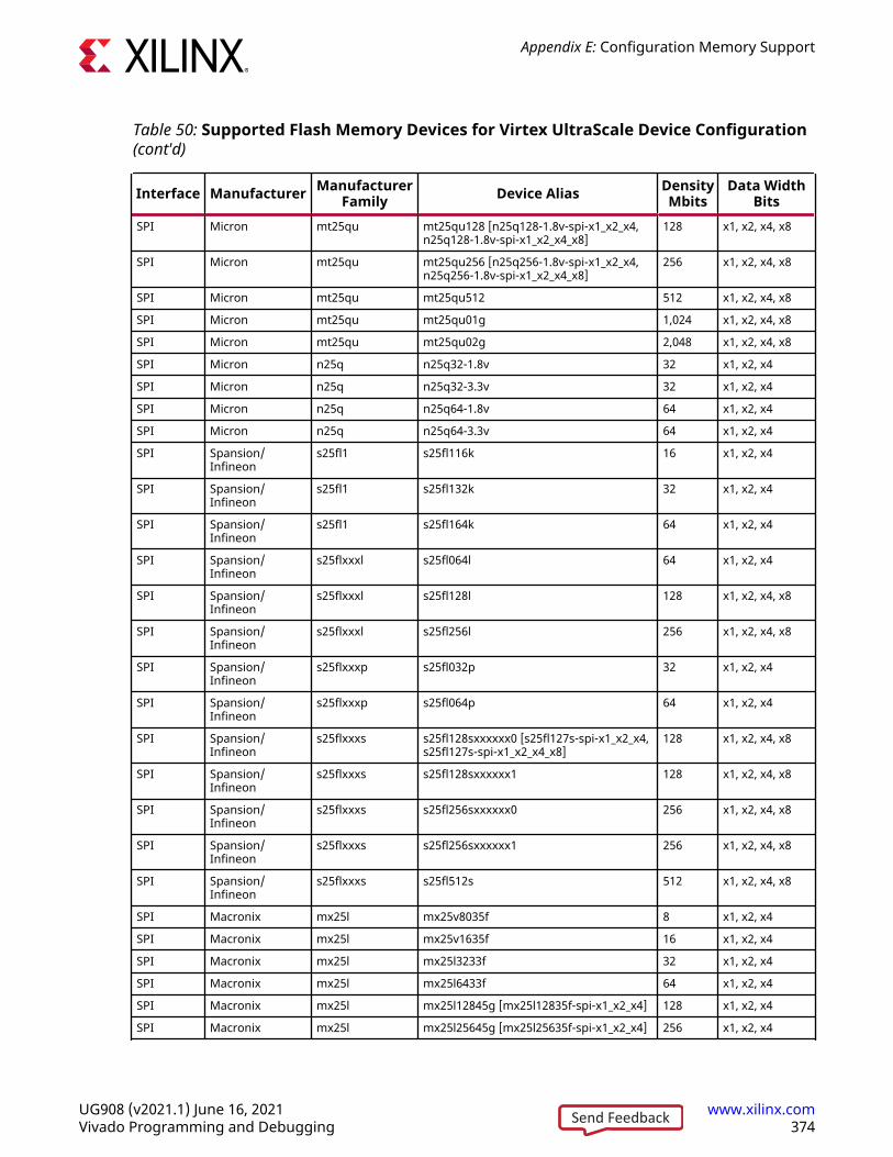
Table 50: Supported Flash Memory Devices for Virtex UltraScale Device Configuration(cont'd)
Interface Manufacturer ManufacturerFamily Device Alias Density
MbitsData Width
BitsSPI Micron mt25qu mt25qu128 [n25q128-1.8v-spi-x1_x2_x4,
n25q128-1.8v-spi-x1_x2_x4_x8]128 x1, x2, x4, x8
SPI Micron mt25qu mt25qu256 [n25q256-1.8v-spi-x1_x2_x4,n25q256-1.8v-spi-x1_x2_x4_x8]
256 x1, x2, x4, x8
SPI Micron mt25qu mt25qu512 512 x1, x2, x4, x8
SPI Micron mt25qu mt25qu01g 1,024 x1, x2, x4, x8
SPI Micron mt25qu mt25qu02g 2,048 x1, x2, x4, x8
SPI Micron n25q n25q32-1.8v 32 x1, x2, x4
SPI Micron n25q n25q32-3.3v 32 x1, x2, x4
SPI Micron n25q n25q64-1.8v 64 x1, x2, x4
SPI Micron n25q n25q64-3.3v 64 x1, x2, x4
SPI Spansion/Infineon
s25fl1 s25fl116k 16 x1, x2, x4
SPI Spansion/Infineon
s25fl1 s25fl132k 32 x1, x2, x4
SPI Spansion/Infineon
s25fl1 s25fl164k 64 x1, x2, x4
SPI Spansion/Infineon
s25flxxxl s25fl064l 64 x1, x2, x4
SPI Spansion/Infineon
s25flxxxl s25fl128l 128 x1, x2, x4, x8
SPI Spansion/Infineon
s25flxxxl s25fl256l 256 x1, x2, x4, x8
SPI Spansion/Infineon
s25flxxxp s25fl032p 32 x1, x2, x4
SPI Spansion/Infineon
s25flxxxp s25fl064p 64 x1, x2, x4
SPI Spansion/Infineon
s25flxxxs s25fl128sxxxxxx0 [s25fl127s-spi-x1_x2_x4,s25fl127s-spi-x1_x2_x4_x8]
128 x1, x2, x4, x8
SPI Spansion/Infineon
s25flxxxs s25fl128sxxxxxx1 128 x1, x2, x4, x8
SPI Spansion/Infineon
s25flxxxs s25fl256sxxxxxx0 256 x1, x2, x4, x8
SPI Spansion/Infineon
s25flxxxs s25fl256sxxxxxx1 256 x1, x2, x4, x8
SPI Spansion/Infineon
s25flxxxs s25fl512s 512 x1, x2, x4, x8
SPI Macronix mx25l mx25v8035f 8 x1, x2, x4
SPI Macronix mx25l mx25v1635f 16 x1, x2, x4
SPI Macronix mx25l mx25l3233f 32 x1, x2, x4
SPI Macronix mx25l mx25l6433f 64 x1, x2, x4
SPI Macronix mx25l mx25l12845g [mx25l12835f-spi-x1_x2_x4] 128 x1, x2, x4
SPI Macronix mx25l mx25l25645g [mx25l25635f-spi-x1_x2_x4] 256 x1, x2, x4
Appendix E: Configuration Memory Support
UG908 (v2021.1) June 16, 2021 www.xilinx.comVivado Programming and Debugging 374Send Feedback
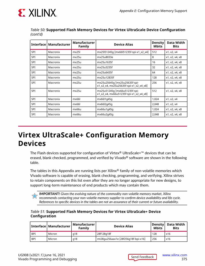
Table 50: Supported Flash Memory Devices for Virtex UltraScale Device Configuration(cont'd)
Interface Manufacturer ManufacturerFamily Device Alias Density
MbitsData Width
BitsSPI Macronix mx25l mx25l51245g [mx66l51235f-spi-x1_x2_x4] 512 x1, x2, x4
SPI Macronix mx25u mx25u8033e 8 x1, x2, x4, x8
SPI Macronix mx25u mx25u1635f 16 x1, x2, x4, x8
SPI Macronix mx25u mx25u3235f 32 x1, x2, x4, x8
SPI Macronix mx25u mx25u6435f 64 x1, x2, x4, x8
SPI Macronix mx25u mx25u12835f 128 x1, x2, x4, x8
SPI Macronix mx25u mx25u25645g [mx25u25635f-spi-x1_x2_x4, mx25u25635f-spi-x1_x2_x4_x8]
256 x1, x2, x4, x8
SPI Macronix mx25u mx25u51245g [mx66u51235f-spi-x1_x2_x4, mx66u51235f-spi-x1_x2_x4_x8]
512 x1, x2, x4, x8
SPI Macronix mx66l mx66l1g45g 1,024 x1, x2, x4
SPI Macronix mx66l mx66l2g45g 2,048 x1, x2, x4
SPI Macronix mx66u mx66u1g45g 1,024 x1, x2, x4, x8
SPI Macronix mx66u mx66u2g45g 2,048 x1, x2, x4, x8
Virtex UltraScale+ Configuration MemoryDevices
The Flash devices supported for configuration of Virtex® UltraScale+™ devices that can beerased, blank checked, programmed, and verified by Vivado® software are shown in the followingtable.
The tables in this Appendix are running lists per Xilinx® family of non-volatile memories whichVivado software is capable of erasing, blank checking, programming, and verifying. Xilinx strivesto retain components on this list even after they are no longer appropriate for new designs, tosupport long-term maintenance of end products which may contain them.
IMPORTANT! Given the evolving nature of the commodity non-volatile memory market, Xilinxrecommends contacting your non-volatile memory supplier to confirm device availability and life cycle.References to specific devices in the tables are not an assurance of their current or future availability.
Table 51: Supported Flash Memory Devices for Virtex UltraScale+ DeviceConfiguration
Interface Manufacturer ManufacturerFamily Device Alias Density
MbitsData Width
BitsBPI Micron g18 28f128g18f 128 x16
BPI Micron g18 mt28gu256aax1e [28f256g18f-bpi-x16] 256 x16
Appendix E: Configuration Memory Support
UG908 (v2021.1) June 16, 2021 www.xilinx.comVivado Programming and Debugging 375Send Feedback
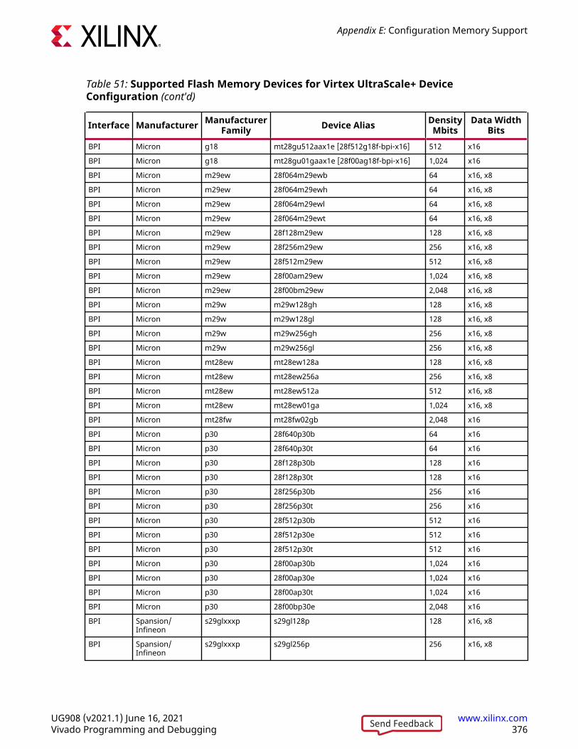
Table 51: Supported Flash Memory Devices for Virtex UltraScale+ DeviceConfiguration (cont'd)
Interface Manufacturer ManufacturerFamily Device Alias Density
MbitsData Width
BitsBPI Micron g18 mt28gu512aax1e [28f512g18f-bpi-x16] 512 x16
BPI Micron g18 mt28gu01gaax1e [28f00ag18f-bpi-x16] 1,024 x16
BPI Micron m29ew 28f064m29ewb 64 x16, x8
BPI Micron m29ew 28f064m29ewh 64 x16, x8
BPI Micron m29ew 28f064m29ewl 64 x16, x8
BPI Micron m29ew 28f064m29ewt 64 x16, x8
BPI Micron m29ew 28f128m29ew 128 x16, x8
BPI Micron m29ew 28f256m29ew 256 x16, x8
BPI Micron m29ew 28f512m29ew 512 x16, x8
BPI Micron m29ew 28f00am29ew 1,024 x16, x8
BPI Micron m29ew 28f00bm29ew 2,048 x16, x8
BPI Micron m29w m29w128gh 128 x16, x8
BPI Micron m29w m29w128gl 128 x16, x8
BPI Micron m29w m29w256gh 256 x16, x8
BPI Micron m29w m29w256gl 256 x16, x8
BPI Micron mt28ew mt28ew128a 128 x16, x8
BPI Micron mt28ew mt28ew256a 256 x16, x8
BPI Micron mt28ew mt28ew512a 512 x16, x8
BPI Micron mt28ew mt28ew01ga 1,024 x16, x8
BPI Micron mt28fw mt28fw02gb 2,048 x16
BPI Micron p30 28f640p30b 64 x16
BPI Micron p30 28f640p30t 64 x16
BPI Micron p30 28f128p30b 128 x16
BPI Micron p30 28f128p30t 128 x16
BPI Micron p30 28f256p30b 256 x16
BPI Micron p30 28f256p30t 256 x16
BPI Micron p30 28f512p30b 512 x16
BPI Micron p30 28f512p30e 512 x16
BPI Micron p30 28f512p30t 512 x16
BPI Micron p30 28f00ap30b 1,024 x16
BPI Micron p30 28f00ap30e 1,024 x16
BPI Micron p30 28f00ap30t 1,024 x16
BPI Micron p30 28f00bp30e 2,048 x16
BPI Spansion/Infineon
s29glxxxp s29gl128p 128 x16, x8
BPI Spansion/Infineon
s29glxxxp s29gl256p 256 x16, x8
Appendix E: Configuration Memory Support
UG908 (v2021.1) June 16, 2021 www.xilinx.comVivado Programming and Debugging 376Send Feedback
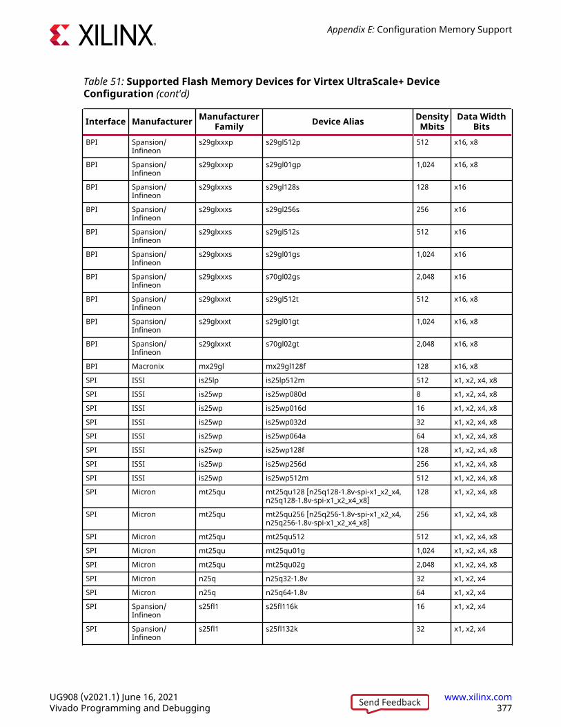
Table 51: Supported Flash Memory Devices for Virtex UltraScale+ DeviceConfiguration (cont'd)
Interface Manufacturer ManufacturerFamily Device Alias Density
MbitsData Width
BitsBPI Spansion/
Infineons29glxxxp s29gl512p 512 x16, x8
BPI Spansion/Infineon
s29glxxxp s29gl01gp 1,024 x16, x8
BPI Spansion/Infineon
s29glxxxs s29gl128s 128 x16
BPI Spansion/Infineon
s29glxxxs s29gl256s 256 x16
BPI Spansion/Infineon
s29glxxxs s29gl512s 512 x16
BPI Spansion/Infineon
s29glxxxs s29gl01gs 1,024 x16
BPI Spansion/Infineon
s29glxxxs s70gl02gs 2,048 x16
BPI Spansion/Infineon
s29glxxxt s29gl512t 512 x16, x8
BPI Spansion/Infineon
s29glxxxt s29gl01gt 1,024 x16, x8
BPI Spansion/Infineon
s29glxxxt s70gl02gt 2,048 x16, x8
BPI Macronix mx29gl mx29gl128f 128 x16, x8
SPI ISSI is25lp is25lp512m 512 x1, x2, x4, x8
SPI ISSI is25wp is25wp080d 8 x1, x2, x4, x8
SPI ISSI is25wp is25wp016d 16 x1, x2, x4, x8
SPI ISSI is25wp is25wp032d 32 x1, x2, x4, x8
SPI ISSI is25wp is25wp064a 64 x1, x2, x4, x8
SPI ISSI is25wp is25wp128f 128 x1, x2, x4, x8
SPI ISSI is25wp is25wp256d 256 x1, x2, x4, x8
SPI ISSI is25wp is25wp512m 512 x1, x2, x4, x8
SPI Micron mt25qu mt25qu128 [n25q128-1.8v-spi-x1_x2_x4,n25q128-1.8v-spi-x1_x2_x4_x8]
128 x1, x2, x4, x8
SPI Micron mt25qu mt25qu256 [n25q256-1.8v-spi-x1_x2_x4,n25q256-1.8v-spi-x1_x2_x4_x8]
256 x1, x2, x4, x8
SPI Micron mt25qu mt25qu512 512 x1, x2, x4, x8
SPI Micron mt25qu mt25qu01g 1,024 x1, x2, x4, x8
SPI Micron mt25qu mt25qu02g 2,048 x1, x2, x4, x8
SPI Micron n25q n25q32-1.8v 32 x1, x2, x4
SPI Micron n25q n25q64-1.8v 64 x1, x2, x4
SPI Spansion/Infineon
s25fl1 s25fl116k 16 x1, x2, x4
SPI Spansion/Infineon
s25fl1 s25fl132k 32 x1, x2, x4
Appendix E: Configuration Memory Support
UG908 (v2021.1) June 16, 2021 www.xilinx.comVivado Programming and Debugging 377Send Feedback
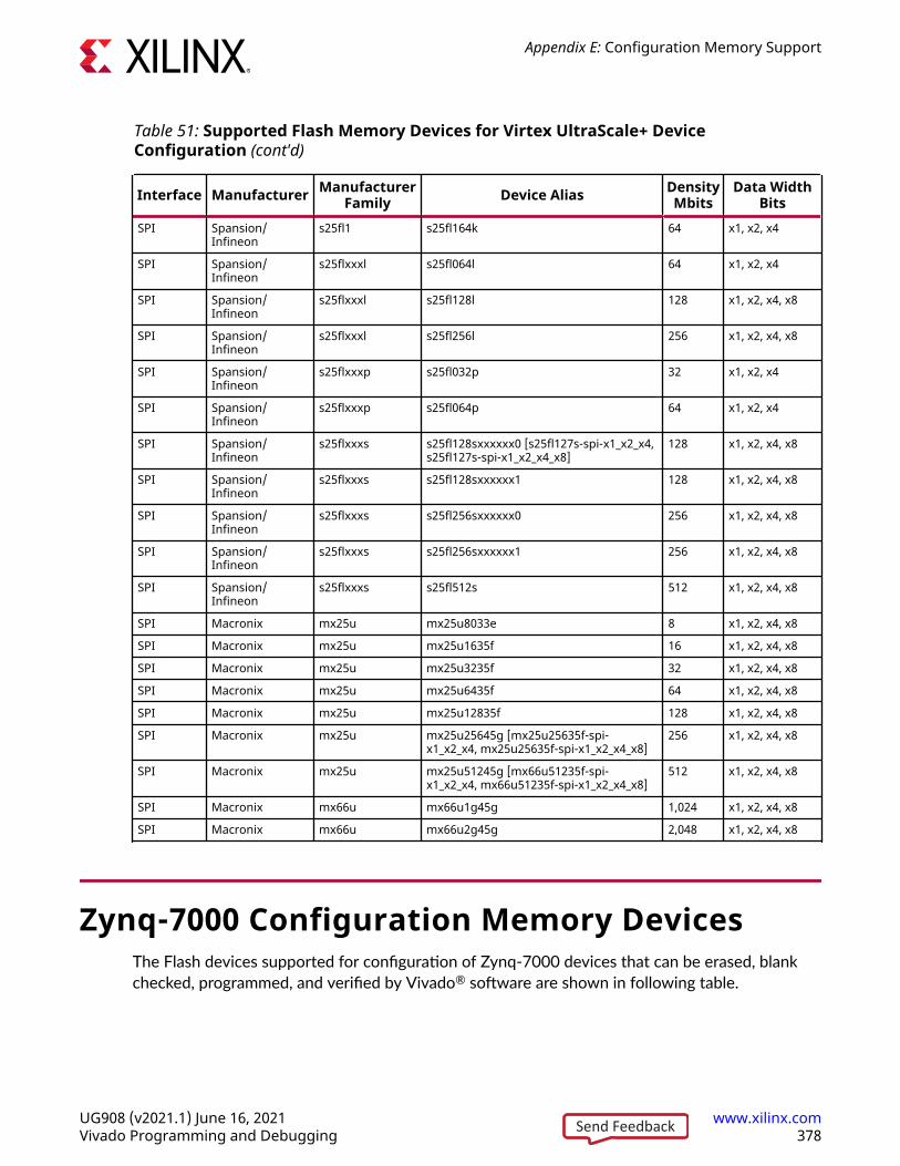
Table 51: Supported Flash Memory Devices for Virtex UltraScale+ DeviceConfiguration (cont'd)
Interface Manufacturer ManufacturerFamily Device Alias Density
MbitsData Width
BitsSPI Spansion/
Infineons25fl1 s25fl164k 64 x1, x2, x4
SPI Spansion/Infineon
s25flxxxl s25fl064l 64 x1, x2, x4
SPI Spansion/Infineon
s25flxxxl s25fl128l 128 x1, x2, x4, x8
SPI Spansion/Infineon
s25flxxxl s25fl256l 256 x1, x2, x4, x8
SPI Spansion/Infineon
s25flxxxp s25fl032p 32 x1, x2, x4
SPI Spansion/Infineon
s25flxxxp s25fl064p 64 x1, x2, x4
SPI Spansion/Infineon
s25flxxxs s25fl128sxxxxxx0 [s25fl127s-spi-x1_x2_x4,s25fl127s-spi-x1_x2_x4_x8]
128 x1, x2, x4, x8
SPI Spansion/Infineon
s25flxxxs s25fl128sxxxxxx1 128 x1, x2, x4, x8
SPI Spansion/Infineon
s25flxxxs s25fl256sxxxxxx0 256 x1, x2, x4, x8
SPI Spansion/Infineon
s25flxxxs s25fl256sxxxxxx1 256 x1, x2, x4, x8
SPI Spansion/Infineon
s25flxxxs s25fl512s 512 x1, x2, x4, x8
SPI Macronix mx25u mx25u8033e 8 x1, x2, x4, x8
SPI Macronix mx25u mx25u1635f 16 x1, x2, x4, x8
SPI Macronix mx25u mx25u3235f 32 x1, x2, x4, x8
SPI Macronix mx25u mx25u6435f 64 x1, x2, x4, x8
SPI Macronix mx25u mx25u12835f 128 x1, x2, x4, x8
SPI Macronix mx25u mx25u25645g [mx25u25635f-spi-x1_x2_x4, mx25u25635f-spi-x1_x2_x4_x8]
256 x1, x2, x4, x8
SPI Macronix mx25u mx25u51245g [mx66u51235f-spi-x1_x2_x4, mx66u51235f-spi-x1_x2_x4_x8]
512 x1, x2, x4, x8
SPI Macronix mx66u mx66u1g45g 1,024 x1, x2, x4, x8
SPI Macronix mx66u mx66u2g45g 2,048 x1, x2, x4, x8
Zynq-7000 Configuration Memory DevicesThe Flash devices supported for configuration of Zynq-7000 devices that can be erased, blankchecked, programmed, and verified by Vivado® software are shown in following table.
Appendix E: Configuration Memory Support
UG908 (v2021.1) June 16, 2021 www.xilinx.comVivado Programming and Debugging 378Send Feedback
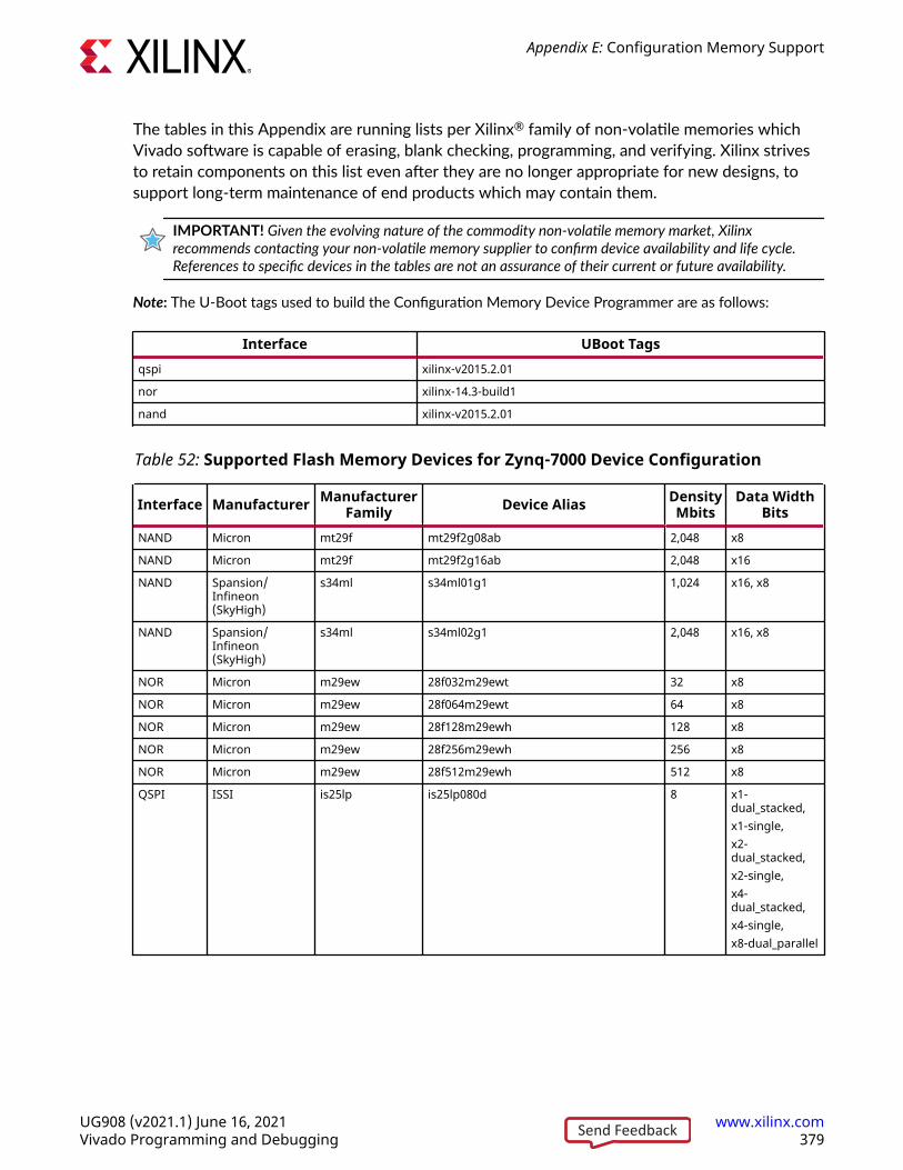
The tables in this Appendix are running lists per Xilinx® family of non-volatile memories whichVivado software is capable of erasing, blank checking, programming, and verifying. Xilinx strivesto retain components on this list even after they are no longer appropriate for new designs, tosupport long-term maintenance of end products which may contain them.
IMPORTANT! Given the evolving nature of the commodity non-volatile memory market, Xilinxrecommends contacting your non-volatile memory supplier to confirm device availability and life cycle.References to specific devices in the tables are not an assurance of their current or future availability.
Note: The U-Boot tags used to build the Configuration Memory Device Programmer are as follows:
Interface UBoot Tagsqspi xilinx-v2015.2.01
nor xilinx-14.3-build1
nand xilinx-v2015.2.01
Table 52: Supported Flash Memory Devices for Zynq-7000 Device Configuration
Interface Manufacturer ManufacturerFamily Device Alias Density
MbitsData Width
BitsNAND Micron mt29f mt29f2g08ab 2,048 x8
NAND Micron mt29f mt29f2g16ab 2,048 x16
NAND Spansion/Infineon(SkyHigh)
s34ml s34ml01g1 1,024 x16, x8
NAND Spansion/Infineon(SkyHigh)
s34ml s34ml02g1 2,048 x16, x8
NOR Micron m29ew 28f032m29ewt 32 x8
NOR Micron m29ew 28f064m29ewt 64 x8
NOR Micron m29ew 28f128m29ewh 128 x8
NOR Micron m29ew 28f256m29ewh 256 x8
NOR Micron m29ew 28f512m29ewh 512 x8
QSPI ISSI is25lp is25lp080d 8 x1-dual_stacked,x1-single,x2-dual_stacked,x2-single,x4-dual_stacked,x4-single,x8-dual_parallel
Appendix E: Configuration Memory Support
UG908 (v2021.1) June 16, 2021 www.xilinx.comVivado Programming and Debugging 379Send Feedback
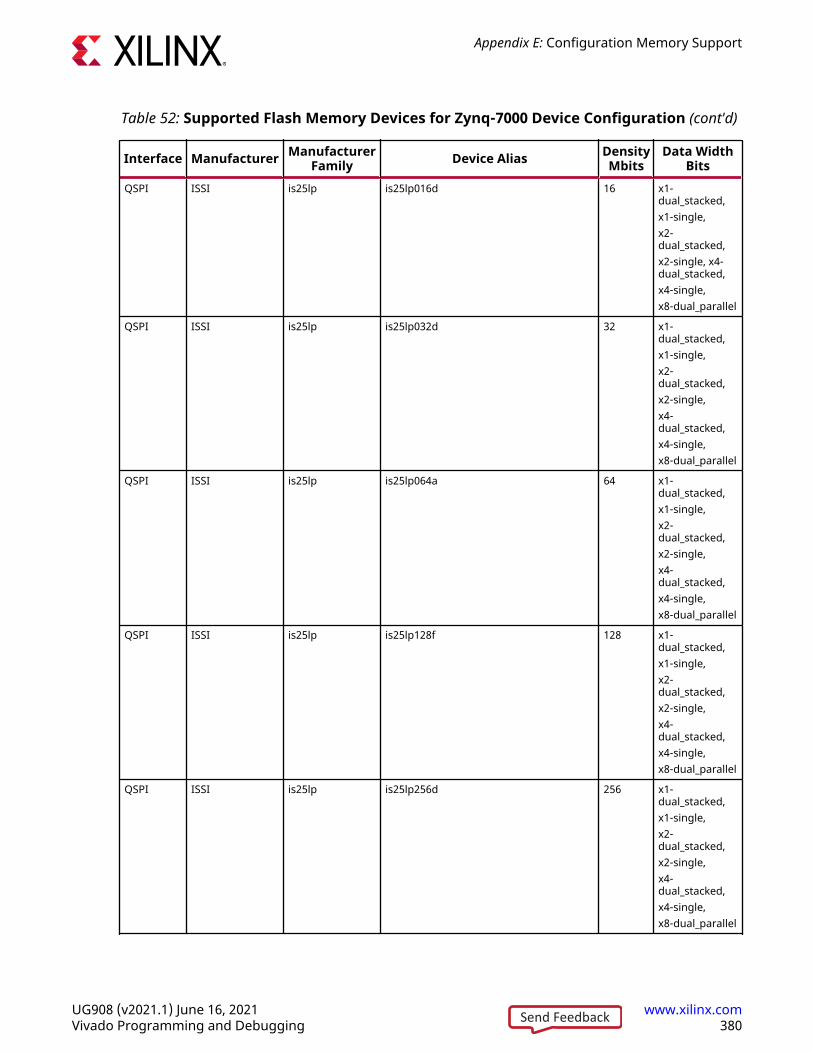
Table 52: Supported Flash Memory Devices for Zynq-7000 Device Configuration (cont'd)
Interface Manufacturer ManufacturerFamily Device Alias Density
MbitsData Width
BitsQSPI ISSI is25lp is25lp016d 16 x1-
dual_stacked,x1-single,x2-dual_stacked,x2-single, x4-dual_stacked,x4-single,x8-dual_parallel
QSPI ISSI is25lp is25lp032d 32 x1-dual_stacked,x1-single,x2-dual_stacked,x2-single,x4-dual_stacked,x4-single,x8-dual_parallel
QSPI ISSI is25lp is25lp064a 64 x1-dual_stacked,x1-single,x2-dual_stacked,x2-single,x4-dual_stacked,x4-single,x8-dual_parallel
QSPI ISSI is25lp is25lp128f 128 x1-dual_stacked,x1-single,x2-dual_stacked,x2-single,x4-dual_stacked,x4-single,x8-dual_parallel
QSPI ISSI is25lp is25lp256d 256 x1-dual_stacked,x1-single,x2-dual_stacked,x2-single,x4-dual_stacked,x4-single,x8-dual_parallel
Appendix E: Configuration Memory Support
UG908 (v2021.1) June 16, 2021 www.xilinx.comVivado Programming and Debugging 380Send Feedback

Table 52: Supported Flash Memory Devices for Zynq-7000 Device Configuration (cont'd)
Interface Manufacturer ManufacturerFamily Device Alias Density
MbitsData Width
BitsQSPI ISSI is25lp is25lp512m 512 x1-
dual_stacked,x1-single,x2-dual_stacked,x2-single,x4-dual_stacked,x4-single,x8-dual_parallel
QSPI ISSI is25wp is25wp080d 8 x1-dual_stacked,x1-single,x2-dual_stacked,x2-single,x4-dual_stacked,x4-single,x8-dual_parallel
QSPI ISSI is25wp is25wp016d 16 x1-dual_stacked,x1-single,x2-dual_stacked,x2-single,x4-dual_stacked,x4-single,x8-dual_parallel
QSPI ISSI is25wp is25wp032d 32 x1-dual_stacked,x1-single,x2-dual_stacked,x2-single,x4-dual_stacked,x4-single,x8-dual_parallel
QSPI ISSI is25wp is25wp064a 64 x1-dual_stacked,x1-single, x2-dual_stacked,x2-single, x4-dual_stacked,x4-single, x8-dual_parallel
Appendix E: Configuration Memory Support
UG908 (v2021.1) June 16, 2021 www.xilinx.comVivado Programming and Debugging 381Send Feedback
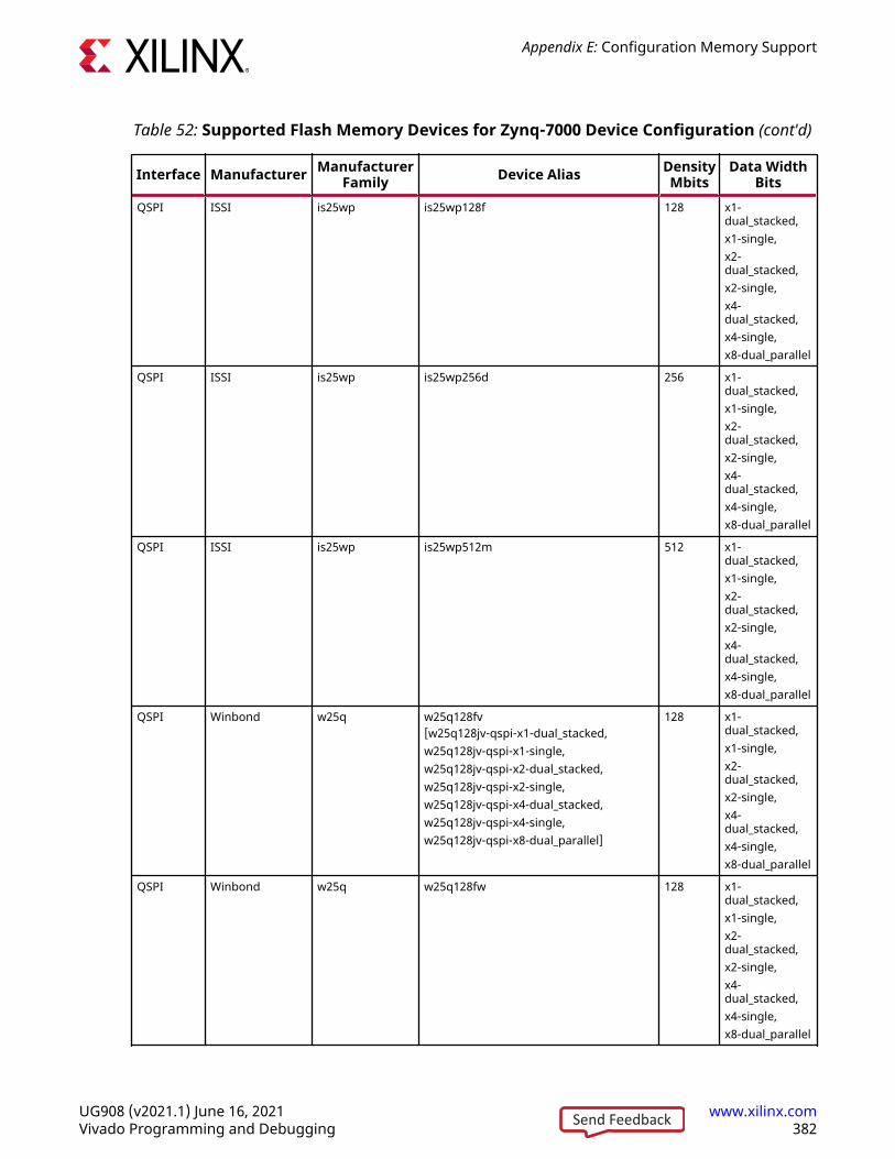
Table 52: Supported Flash Memory Devices for Zynq-7000 Device Configuration (cont'd)
Interface Manufacturer ManufacturerFamily Device Alias Density
MbitsData Width
BitsQSPI ISSI is25wp is25wp128f 128 x1-
dual_stacked,x1-single,x2-dual_stacked,x2-single,x4-dual_stacked,x4-single,x8-dual_parallel
QSPI ISSI is25wp is25wp256d 256 x1-dual_stacked,x1-single,x2-dual_stacked,x2-single,x4-dual_stacked,x4-single,x8-dual_parallel
QSPI ISSI is25wp is25wp512m 512 x1-dual_stacked,x1-single,x2-dual_stacked,x2-single,x4-dual_stacked,x4-single,x8-dual_parallel
QSPI Winbond w25q w25q128fv[w25q128jv-qspi-x1-dual_stacked,w25q128jv-qspi-x1-single,w25q128jv-qspi-x2-dual_stacked,w25q128jv-qspi-x2-single,w25q128jv-qspi-x4-dual_stacked,w25q128jv-qspi-x4-single,w25q128jv-qspi-x8-dual_parallel]
128 x1-dual_stacked,x1-single,x2-dual_stacked,x2-single,x4-dual_stacked,x4-single,x8-dual_parallel
QSPI Winbond w25q w25q128fw 128 x1-dual_stacked,x1-single,x2-dual_stacked,x2-single,x4-dual_stacked,x4-single,x8-dual_parallel
Appendix E: Configuration Memory Support
UG908 (v2021.1) June 16, 2021 www.xilinx.comVivado Programming and Debugging 382Send Feedback
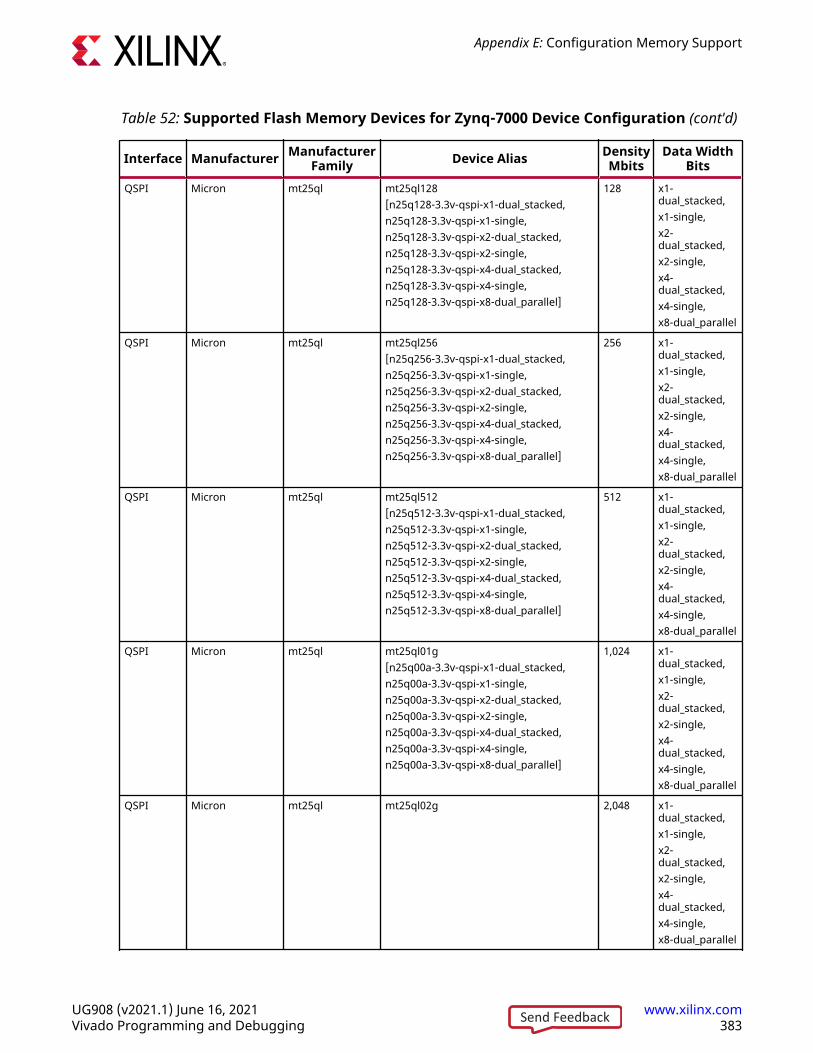
Table 52: Supported Flash Memory Devices for Zynq-7000 Device Configuration (cont'd)
Interface Manufacturer ManufacturerFamily Device Alias Density
MbitsData Width
BitsQSPI Micron mt25ql mt25ql128
[n25q128-3.3v-qspi-x1-dual_stacked,n25q128-3.3v-qspi-x1-single,n25q128-3.3v-qspi-x2-dual_stacked,n25q128-3.3v-qspi-x2-single,n25q128-3.3v-qspi-x4-dual_stacked,n25q128-3.3v-qspi-x4-single,n25q128-3.3v-qspi-x8-dual_parallel]
128 x1-dual_stacked,x1-single,x2-dual_stacked,x2-single,x4-dual_stacked,x4-single,x8-dual_parallel
QSPI Micron mt25ql mt25ql256[n25q256-3.3v-qspi-x1-dual_stacked,n25q256-3.3v-qspi-x1-single,n25q256-3.3v-qspi-x2-dual_stacked,n25q256-3.3v-qspi-x2-single,n25q256-3.3v-qspi-x4-dual_stacked,n25q256-3.3v-qspi-x4-single,n25q256-3.3v-qspi-x8-dual_parallel]
256 x1-dual_stacked,x1-single,x2-dual_stacked,x2-single,x4-dual_stacked,x4-single,x8-dual_parallel
QSPI Micron mt25ql mt25ql512[n25q512-3.3v-qspi-x1-dual_stacked,n25q512-3.3v-qspi-x1-single,n25q512-3.3v-qspi-x2-dual_stacked,n25q512-3.3v-qspi-x2-single,n25q512-3.3v-qspi-x4-dual_stacked,n25q512-3.3v-qspi-x4-single,n25q512-3.3v-qspi-x8-dual_parallel]
512 x1-dual_stacked,x1-single,x2-dual_stacked,x2-single,x4-dual_stacked,x4-single,x8-dual_parallel
QSPI Micron mt25ql mt25ql01g[n25q00a-3.3v-qspi-x1-dual_stacked,n25q00a-3.3v-qspi-x1-single,n25q00a-3.3v-qspi-x2-dual_stacked,n25q00a-3.3v-qspi-x2-single,n25q00a-3.3v-qspi-x4-dual_stacked,n25q00a-3.3v-qspi-x4-single,n25q00a-3.3v-qspi-x8-dual_parallel]
1,024 x1-dual_stacked,x1-single,x2-dual_stacked,x2-single,x4-dual_stacked,x4-single,x8-dual_parallel
QSPI Micron mt25ql mt25ql02g 2,048 x1-dual_stacked,x1-single,x2-dual_stacked,x2-single,x4-dual_stacked,x4-single,x8-dual_parallel
Appendix E: Configuration Memory Support
UG908 (v2021.1) June 16, 2021 www.xilinx.comVivado Programming and Debugging 383Send Feedback

Table 52: Supported Flash Memory Devices for Zynq-7000 Device Configuration (cont'd)
Interface Manufacturer ManufacturerFamily Device Alias Density
MbitsData Width
BitsQSPI Micron mt25qu mt25qu128
[n25q128-1.8v-qspi-x1-dual_stacked,n25q128-1.8v-qspi-x1-single,n25q128-1.8v-qspi-x2-dual_stacked,n25q128-1.8v-qspi-x2-single,n25q128-1.8v-qspi-x4-dual_stacked,n25q128-1.8v-qspi-x4-single,n25q128-1.8v-qspi-x8-dual_parallel]
128 x1-dual_stacked,x1-single,x2-dual_stacked,x2-single,x4-dual_stacked,x4-single,x8-dual_parallel
QSPI Micron mt25qu mt25qu256[n25q256-1.8v-qspi-x1-dual_stacked,n25q256-1.8v-qspi-x1-single,n25q256-1.8v-qspi-x2-dual_stacked,n25q256-1.8v-qspi-x2-single,n25q256-1.8v-qspi-x4-dual_stacked,n25q256-1.8v-qspi-x4-single,n25q256-1.8v-qspi-x8-dual_parallel]
256 x1-dual_stacked,x1-single,x2-dual_stacked,x2-single,x4-dual_stacked,x4-single,x8-dual_parallel
QSPI Micron mt25qu mt25qu512[n25q512-1.8v-qspi-x1-dual_stacked,n25q512-1.8v-qspi-x1-single,n25q512-1.8v-qspi-x2-dual_stacked,n25q512-1.8v-qspi-x2-single,n25q512-1.8v-qspi-x4-dual_stacked,n25q512-1.8v-qspi-x4-single,n25q512-1.8v-qspi-x8-dual_parallel]
512 x1-dual_stacked,x1-single,x2-dual_stacked,x2-single,x4-dual_stacked,x4-single,x8-dual_parallel
QSPI Micron mt25qu mt25qu01g[n25q00a-1.8v-qspi-x1-dual_stacked,n25q00a-1.8v-qspi-x1-single,n25q00a-1.8v-qspi-x2-dual_stacked,n25q00a-1.8v-qspi-x2-single,n25q00a-1.8v-qspi-x4-dual_stacked,n25q00a-1.8v-qspi-x4-single,n25q00a-1.8v-qspi-x8-dual_parallel]
1,024 x1-dual_stacked,x1-single,x2-dual_stacked,x2-single,x4-dual_stacked,x4-single,x8-dual_parallel
QSPI Micron mt25qu mt25qu02g 2,048 x1-dual_stacked,x1-single,x2-dual_stacked,x2-single,x4-dual_stacked,x4-single,x8-dual_parallel
Appendix E: Configuration Memory Support
UG908 (v2021.1) June 16, 2021 www.xilinx.comVivado Programming and Debugging 384Send Feedback
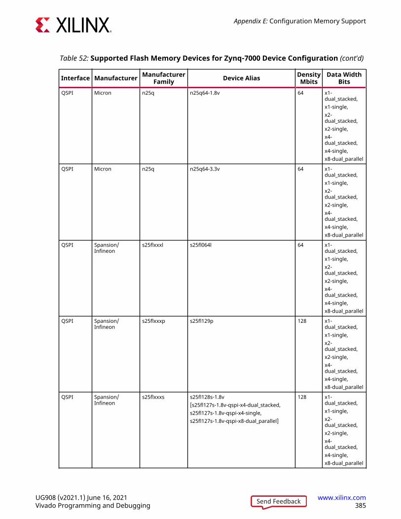
Table 52: Supported Flash Memory Devices for Zynq-7000 Device Configuration (cont'd)
Interface Manufacturer ManufacturerFamily Device Alias Density
MbitsData Width
BitsQSPI Micron n25q n25q64-1.8v 64 x1-
dual_stacked,x1-single,x2-dual_stacked,x2-single,x4-dual_stacked,x4-single,x8-dual_parallel
QSPI Micron n25q n25q64-3.3v 64 x1-dual_stacked,x1-single,x2-dual_stacked,x2-single,x4-dual_stacked,x4-single,x8-dual_parallel
QSPI Spansion/Infineon
s25flxxxl s25fl064l 64 x1-dual_stacked,x1-single,x2-dual_stacked,x2-single,x4-dual_stacked,x4-single,x8-dual_parallel
QSPI Spansion/Infineon
s25flxxxp s25fl129p 128 x1-dual_stacked,x1-single,x2-dual_stacked,x2-single,x4-dual_stacked,x4-single,x8-dual_parallel
QSPI Spansion/Infineon
s25flxxxs s25fl128s-1.8v[s25fl127s-1.8v-qspi-x4-dual_stacked,s25fl127s-1.8v-qspi-x4-single,s25fl127s-1.8v-qspi-x8-dual_parallel]
128 x1-dual_stacked,x1-single,x2-dual_stacked,x2-single,x4-dual_stacked,x4-single,x8-dual_parallel
Appendix E: Configuration Memory Support
UG908 (v2021.1) June 16, 2021 www.xilinx.comVivado Programming and Debugging 385Send Feedback
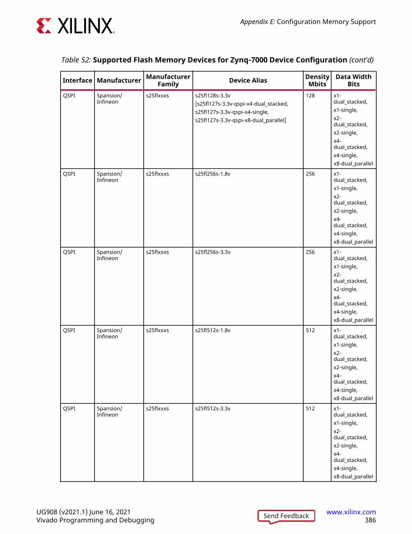
Table 52: Supported Flash Memory Devices for Zynq-7000 Device Configuration (cont'd)
Interface Manufacturer ManufacturerFamily Device Alias Density
MbitsData Width
BitsQSPI Spansion/
Infineons25flxxxs s25fl128s-3.3v
[s25fl127s-3.3v-qspi-x4-dual_stacked,s25fl127s-3.3v-qspi-x4-single,s25fl127s-3.3v-qspi-x8-dual_parallel]
128 x1-dual_stacked,x1-single,x2-dual_stacked,x2-single,x4-dual_stacked,x4-single,x8-dual_parallel
QSPI Spansion/Infineon
s25flxxxs s25fl256s-1.8v 256 x1-dual_stacked,x1-single,x2-dual_stacked,x2-single,x4-dual_stacked,x4-single,x8-dual_parallel
QSPI Spansion/Infineon
s25flxxxs s25fl256s-3.3v 256 x1-dual_stacked,x1-single,x2-dual_stacked,x2-single,x4-dual_stacked,x4-single,x8-dual_parallel
QSPI Spansion/Infineon
s25flxxxs s25fl512s-1.8v 512 x1-dual_stacked,x1-single,x2-dual_stacked,x2-single,x4-dual_stacked,x4-single,x8-dual_parallel
QSPI Spansion/Infineon
s25flxxxs s25fl512s-3.3v 512 x1-dual_stacked,x1-single,x2-dual_stacked,x2-single,x4-dual_stacked,x4-single,x8-dual_parallel
Appendix E: Configuration Memory Support
UG908 (v2021.1) June 16, 2021 www.xilinx.comVivado Programming and Debugging 386Send Feedback
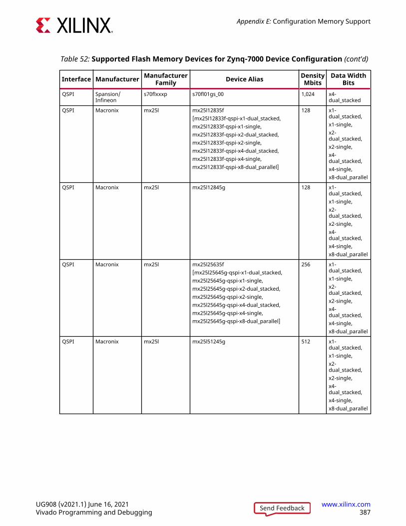
Table 52: Supported Flash Memory Devices for Zynq-7000 Device Configuration (cont'd)
Interface Manufacturer ManufacturerFamily Device Alias Density
MbitsData Width
BitsQSPI Spansion/
Infineons70flxxxp s70fl01gs_00 1,024 x4-
dual_stacked
QSPI Macronix mx25l mx25l12835f[mx25l12833f-qspi-x1-dual_stacked,mx25l12833f-qspi-x1-single,mx25l12833f-qspi-x2-dual_stacked,mx25l12833f-qspi-x2-single,mx25l12833f-qspi-x4-dual_stacked,mx25l12833f-qspi-x4-single,mx25l12833f-qspi-x8-dual_parallel]
128 x1-dual_stacked,x1-single,x2-dual_stacked,x2-single,x4-dual_stacked,x4-single,x8-dual_parallel
QSPI Macronix mx25l mx25l12845g 128 x1-dual_stacked,x1-single,x2-dual_stacked,x2-single,x4-dual_stacked,x4-single,x8-dual_parallel
QSPI Macronix mx25l mx25l25635f[mx25l25645g-qspi-x1-dual_stacked,mx25l25645g-qspi-x1-single,mx25l25645g-qspi-x2-dual_stacked,mx25l25645g-qspi-x2-single,mx25l25645g-qspi-x4-dual_stacked,mx25l25645g-qspi-x4-single,mx25l25645g-qspi-x8-dual_parallel]
256 x1-dual_stacked,x1-single,x2-dual_stacked,x2-single,x4-dual_stacked,x4-single,x8-dual_parallel
QSPI Macronix mx25l mx25l51245g 512 x1-dual_stacked,x1-single,x2-dual_stacked,x2-single,x4-dual_stacked,x4-single,x8-dual_parallel
Appendix E: Configuration Memory Support
UG908 (v2021.1) June 16, 2021 www.xilinx.comVivado Programming and Debugging 387Send Feedback
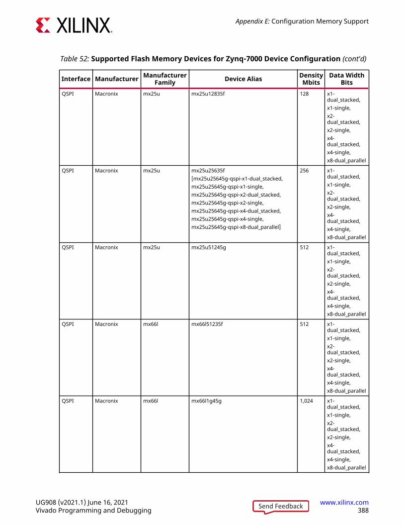
Table 52: Supported Flash Memory Devices for Zynq-7000 Device Configuration (cont'd)
Interface Manufacturer ManufacturerFamily Device Alias Density
MbitsData Width
BitsQSPI Macronix mx25u mx25u12835f 128 x1-
dual_stacked,x1-single,x2-dual_stacked,x2-single,x4-dual_stacked,x4-single,x8-dual_parallel
QSPI Macronix mx25u mx25u25635f[mx25u25645g-qspi-x1-dual_stacked,mx25u25645g-qspi-x1-single,mx25u25645g-qspi-x2-dual_stacked,mx25u25645g-qspi-x2-single,mx25u25645g-qspi-x4-dual_stacked,mx25u25645g-qspi-x4-single,mx25u25645g-qspi-x8-dual_parallel]
256 x1-dual_stacked,x1-single,x2-dual_stacked,x2-single,x4-dual_stacked,x4-single,x8-dual_parallel
QSPI Macronix mx25u mx25u51245g 512 x1-dual_stacked,x1-single,x2-dual_stacked,x2-single,x4-dual_stacked,x4-single,x8-dual_parallel
QSPI Macronix mx66l mx66l51235f 512 x1-dual_stacked,x1-single,x2-dual_stacked,x2-single,x4-dual_stacked,x4-single,x8-dual_parallel
QSPI Macronix mx66l mx66l1g45g 1,024 x1-dual_stacked,x1-single,x2-dual_stacked,x2-single,x4-dual_stacked,x4-single,x8-dual_parallel
Appendix E: Configuration Memory Support
UG908 (v2021.1) June 16, 2021 www.xilinx.comVivado Programming and Debugging 388Send Feedback
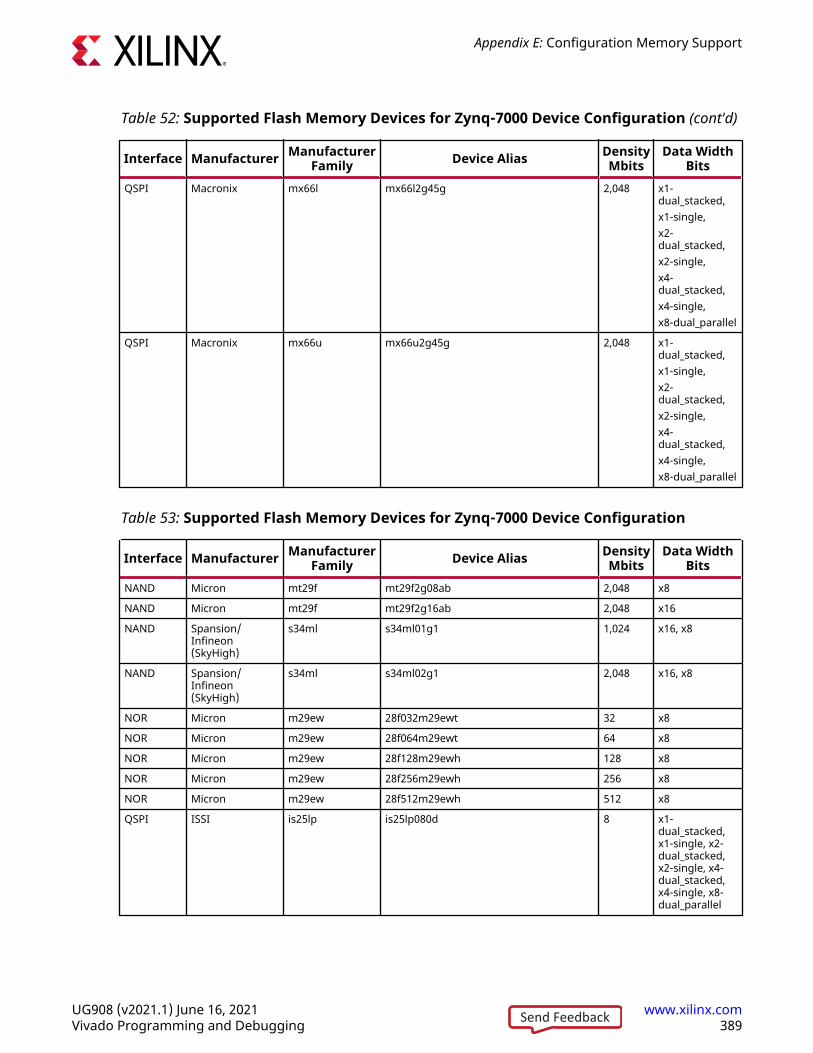
Table 52: Supported Flash Memory Devices for Zynq-7000 Device Configuration (cont'd)
Interface Manufacturer ManufacturerFamily Device Alias Density
MbitsData Width
BitsQSPI Macronix mx66l mx66l2g45g 2,048 x1-
dual_stacked,x1-single,x2-dual_stacked,x2-single,x4-dual_stacked,x4-single,x8-dual_parallel
QSPI Macronix mx66u mx66u2g45g 2,048 x1-dual_stacked,x1-single,x2-dual_stacked,x2-single,x4-dual_stacked,x4-single,x8-dual_parallel
Table 53: Supported Flash Memory Devices for Zynq-7000 Device Configuration
Interface Manufacturer ManufacturerFamily Device Alias Density
MbitsData Width
BitsNAND Micron mt29f mt29f2g08ab 2,048 x8
NAND Micron mt29f mt29f2g16ab 2,048 x16
NAND Spansion/Infineon(SkyHigh)
s34ml s34ml01g1 1,024 x16, x8
NAND Spansion/Infineon(SkyHigh)
s34ml s34ml02g1 2,048 x16, x8
NOR Micron m29ew 28f032m29ewt 32 x8
NOR Micron m29ew 28f064m29ewt 64 x8
NOR Micron m29ew 28f128m29ewh 128 x8
NOR Micron m29ew 28f256m29ewh 256 x8
NOR Micron m29ew 28f512m29ewh 512 x8
QSPI ISSI is25lp is25lp080d 8 x1-dual_stacked,x1-single, x2-dual_stacked,x2-single, x4-dual_stacked,x4-single, x8-dual_parallel
Appendix E: Configuration Memory Support
UG908 (v2021.1) June 16, 2021 www.xilinx.comVivado Programming and Debugging 389Send Feedback
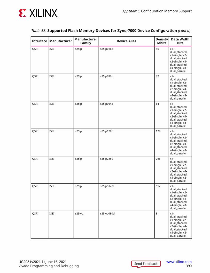
Table 53: Supported Flash Memory Devices for Zynq-7000 Device Configuration (cont'd)
Interface Manufacturer ManufacturerFamily Device Alias Density
MbitsData Width
BitsQSPI ISSI is25lp is25lp016d 16 x1-
dual_stacked,x1-single, x2-dual_stacked,x2-single, x4-dual_stacked,x4-single, x8-dual_parallel
QSPI ISSI is25lp is25lp032d 32 x1-dual_stacked,x1-single, x2-dual_stacked,x2-single, x4-dual_stacked,x4-single, x8-dual_parallel
QSPI ISSI is25lp is25lp064a 64 x1-dual_stacked,x1-single, x2-dual_stacked,x2-single, x4-dual_stacked,x4-single, x8-dual_parallel
QSPI ISSI is25lp is25lp128f 128 x1-dual_stacked,x1-single, x2-dual_stacked,x2-single, x4-dual_stacked,x4-single, x8-dual_parallel
QSPI ISSI is25lp is25lp256d 256 x1-dual_stacked,x1-single, x2-dual_stacked,x2-single, x4-dual_stacked,x4-single, x8-dual_parallel
QSPI ISSI is25lp is25lp512m 512 x1-dual_stacked,x1-single, x2-dual_stacked,x2-single, x4-dual_stacked,x4-single, x8-dual_parallel
QSPI ISSI is25wp is25wp080d 8 x1-dual_stacked,x1-single, x2-dual_stacked,x2-single, x4-dual_stacked,x4-single, x8-dual_parallel
Appendix E: Configuration Memory Support
UG908 (v2021.1) June 16, 2021 www.xilinx.comVivado Programming and Debugging 390Send Feedback
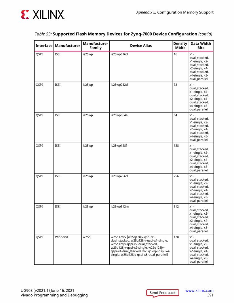
Table 53: Supported Flash Memory Devices for Zynq-7000 Device Configuration (cont'd)
Interface Manufacturer ManufacturerFamily Device Alias Density
MbitsData Width
BitsQSPI ISSI is25wp is25wp016d 16 x1-
dual_stacked,x1-single, x2-dual_stacked,x2-single, x4-dual_stacked,x4-single, x8-dual_parallel
QSPI ISSI is25wp is25wp032d 32 x1-dual_stacked,x1-single, x2-dual_stacked,x2-single, x4-dual_stacked,x4-single, x8-dual_parallel
QSPI ISSI is25wp is25wp064a 64 x1-dual_stacked,x1-single, x2-dual_stacked,x2-single, x4-dual_stacked,x4-single, x8-dual_parallel
QSPI ISSI is25wp is25wp128f 128 x1-dual_stacked,x1-single, x2-dual_stacked,x2-single, x4-dual_stacked,x4-single, x8-dual_parallel
QSPI ISSI is25wp is25wp256d 256 x1-dual_stacked,x1-single, x2-dual_stacked,x2-single, x4-dual_stacked,x4-single, x8-dual_parallel
QSPI ISSI is25wp is25wp512m 512 x1-dual_stacked,x1-single, x2-dual_stacked,x2-single, x4-dual_stacked,x4-single, x8-dual_parallel
QSPI Winbond w25q w25q128fv [w25q128jv-qspi-x1-dual_stacked, w25q128jv-qspi-x1-single,w25q128jv-qspi-x2-dual_stacked,w25q128jv-qspi-x2-single, w25q128jv-qspi-x4-dual_stacked, w25q128jv-qspi-x4-single, w25q128jv-qspi-x8-dual_parallel]
128 x1-dual_stacked,x1-single, x2-dual_stacked,x2-single, x4-dual_stacked,x4-single, x8-dual_parallel
Appendix E: Configuration Memory Support
UG908 (v2021.1) June 16, 2021 www.xilinx.comVivado Programming and Debugging 391Send Feedback
Table 53: Supported Flash Memory Devices for Zynq-7000 Device Configuration (cont'd)
Interface Manufacturer ManufacturerFamily Device Alias Density
MbitsData Width
BitsQSPI Winbond w25q w25q128fw 128 x1-
dual_stacked,x1-single, x2-dual_stacked,x2-single, x4-dual_stacked,x4-single, x8-dual_parallel
QSPI Micron mt25ql mt25ql128 [n25q128-3.3v-qspi-x1-dual_stacked, n25q128-3.3v-qspi-x1-single, n25q128-3.3v-qspi-x2-dual_stacked, n25q128-3.3v-qspi-x2-single, n25q128-3.3v-qspi-x4-dual_stacked, n25q128-3.3v-qspi-x4-single, n25q128-3.3v-qspi-x8-dual_parallel]
128 x1-dual_stacked,x1-single, x2-dual_stacked,x2-single, x4-dual_stacked,x4-single, x8-dual_parallel
QSPI Micron mt25ql mt25ql256 [n25q256-3.3v-qspi-x1-dual_stacked, n25q256-3.3v-qspi-x1-single, n25q256-3.3v-qspi-x2-dual_stacked, n25q256-3.3v-qspi-x2-single, n25q256-3.3v-qspi-x4-dual_stacked, n25q256-3.3v-qspi-x4-single, n25q256-3.3v-qspi-x8-dual_parallel]
256 x1-dual_stacked,x1-single, x2-dual_stacked,x2-single, x4-dual_stacked,x4-single, x8-dual_parallel
QSPI Micron mt25ql mt25ql512 [n25q512-3.3v-qspi-x1-dual_stacked, n25q512-3.3v-qspi-x1-single, n25q512-3.3v-qspi-x2-dual_stacked, n25q512-3.3v-qspi-x2-single, n25q512-3.3v-qspi-x4-dual_stacked, n25q512-3.3v-qspi-x4-single, n25q512-3.3v-qspi-x8-dual_parallel]
512 x1-dual_stacked,x1-single, x2-dual_stacked,x2-single, x4-dual_stacked,x4-single, x8-dual_parallel
QSPI Micron mt25ql mt25ql01g [n25q00a-3.3v-qspi-x1-dual_stacked, n25q00a-3.3v-qspi-x1-single, n25q00a-3.3v-qspi-x2-dual_stacked, n25q00a-3.3v-qspi-x2-single, n25q00a-3.3v-qspi-x4-dual_stacked, n25q00a-3.3v-qspi-x4-single, n25q00a-3.3v-qspi-x8-dual_parallel]
1,024 x1-dual_stacked,x1-single, x2-dual_stacked,x2-single, x4-dual_stacked,x4-single, x8-dual_parallel
QSPI Micron mt25ql mt25ql02g 2,048 x1-dual_stacked,x1-single, x2-dual_stacked,x2-single, x4-dual_stacked,x4-single, x8-dual_parallel
QSPI Micron mt25qu mt25qu128 [n25q128-1.8v-qspi-x1-dual_stacked, n25q128-1.8v-qspi-x1-single, n25q128-1.8v-qspi-x2-dual_stacked, n25q128-1.8v-qspi-x2-single, n25q128-1.8v-qspi-x4-dual_stacked, n25q128-1.8v-qspi-x4-single, n25q128-1.8v-qspi-x8-dual_parallel]
128 x1-dual_stacked,x1-single, x2-dual_stacked,x2-single, x4-dual_stacked,x4-single, x8-dual_parallel
Appendix E: Configuration Memory Support
UG908 (v2021.1) June 16, 2021 www.xilinx.comVivado Programming and Debugging 392Send Feedback
Table 53: Supported Flash Memory Devices for Zynq-7000 Device Configuration (cont'd)
Interface Manufacturer ManufacturerFamily Device Alias Density
MbitsData Width
BitsQSPI Micron mt25qu mt25qu256 [n25q256-1.8v-qspi-x1-
dual_stacked, n25q256-1.8v-qspi-x1-single, n25q256-1.8v-qspi-x2-dual_stacked, n25q256-1.8v-qspi-x2-single, n25q256-1.8v-qspi-x4-dual_stacked, n25q256-1.8v-qspi-x4-single, n25q256-1.8v-qspi-x8-dual_parallel]
256 x1-dual_stacked,x1-single, x2-dual_stacked,x2-single, x4-dual_stacked,x4-single, x8-dual_parallel
QSPI Micron mt25qu mt25qu512 [n25q512-1.8v-qspi-x1-dual_stacked, n25q512-1.8v-qspi-x1-single, n25q512-1.8v-qspi-x2-dual_stacked, n25q512-1.8v-qspi-x2-single, n25q512-1.8v-qspi-x4-dual_stacked, n25q512-1.8v-qspi-x4-single, n25q512-1.8v-qspi-x8-dual_parallel]
512 x1-dual_stacked,x1-single, x2-dual_stacked,x2-single, x4-dual_stacked,x4-single, x8-dual_parallel
QSPI Micron mt25qu mt25qu01g [n25q00a-1.8v-qspi-x1-dual_stacked, n25q00a-1.8v-qspi-x1-single, n25q00a-1.8v-qspi-x2-dual_stacked, n25q00a-1.8v-qspi-x2-single, n25q00a-1.8v-qspi-x4-dual_stacked, n25q00a-1.8v-qspi-x4-single, n25q00a-1.8v-qspi-x8-dual_parallel]
1,024 x1-dual_stacked,x1-single, x2-dual_stacked,x2-single, x4-dual_stacked,x4-single, x8-dual_parallel
QSPI Micron mt25qu mt25qu02g 2,048 x1-dual_stacked,x1-single, x2-dual_stacked,x2-single, x4-dual_stacked,x4-single, x8-dual_parallel
QSPI Micron n25q n25q64-1.8v 64 x1-dual_stacked,x1-single, x2-dual_stacked,x2-single, x4-dual_stacked,x4-single, x8-dual_parallel
QSPI Micron n25q n25q64-3.3v 64 x1-dual_stacked,x1-single, x2-dual_stacked,x2-single, x4-dual_stacked,x4-single, x8-dual_parallel
QSPI Spansion/Infineon
s25flxxxl s25fl064l 64 x1-dual_stacked,x1-single, x2-dual_stacked,x2-single, x4-dual_stacked,x4-single, x8-dual_parallel
Appendix E: Configuration Memory Support
UG908 (v2021.1) June 16, 2021 www.xilinx.comVivado Programming and Debugging 393Send Feedback
Table 53: Supported Flash Memory Devices for Zynq-7000 Device Configuration (cont'd)
Interface Manufacturer ManufacturerFamily Device Alias Density
MbitsData Width
BitsQSPI Spansion/
Infineons25flxxxp s25fl129p 128 x1-
dual_stacked,x1-single, x2-dual_stacked,x2-single, x4-dual_stacked,x4-single, x8-dual_parallel
QSPI Spansion/Infineon
s25flxxxs s25fl128s-1.8v [s25fl127s-1.8v-qspi-x4-dual_stacked, s25fl127s-1.8v-qspi-x4-single, s25fl127s-1.8v-qspi-x8-dual_parallel]
128 x1-dual_stacked,x1-single, x2-dual_stacked,x2-single, x4-dual_stacked,x4-single, x8-dual_parallel
QSPI Spansion/Infineon
s25flxxxs s25fl128s-3.3v [s25fl127s-3.3v-qspi-x4-dual_stacked, s25fl127s-3.3v-qspi-x4-single, s25fl127s-3.3v-qspi-x8-dual_parallel]
128 x1-dual_stacked,x1-single, x2-dual_stacked,x2-single, x4-dual_stacked,x4-single, x8-dual_parallel
QSPI Spansion/Infineon
s25flxxxs s25fl256s-1.8v 256 x1-dual_stacked,x1-single, x2-dual_stacked,x2-single, x4-dual_stacked,x4-single, x8-dual_parallel
QSPI Spansion/Infineon
s25flxxxs s25fl256s-3.3v 256 x1-dual_stacked,x1-single, x2-dual_stacked,x2-single, x4-dual_stacked,x4-single, x8-dual_parallel
QSPI Spansion/Infineon
s25flxxxs s25fl512s-1.8v 512 x1-dual_stacked,x1-single, x2-dual_stacked,x2-single, x4-dual_stacked,x4-single, x8-dual_parallel
QSPI Spansion/Infineon
s25flxxxs s25fl512s-3.3v 512 x1-dual_stacked,x1-single, x2-dual_stacked,x2-single, x4-dual_stacked,x4-single, x8-dual_parallel
QSPI Spansion/Infineon
s70flxxxp s70fl01gs_00 1,024 x4-dual_stacked
Appendix E: Configuration Memory Support
UG908 (v2021.1) June 16, 2021 www.xilinx.comVivado Programming and Debugging 394Send Feedback
Table 53: Supported Flash Memory Devices for Zynq-7000 Device Configuration (cont'd)
Interface Manufacturer ManufacturerFamily Device Alias Density
MbitsData Width
BitsQSPI Macronix mx25l mx25l12835f [mx25l12833f-qspi-x1-
dual_stacked, mx25l12833f-qspi-x1-single,mx25l12833f-qspi-x2-dual_stacked,mx25l12833f-qspi-x2-single, mx25l12833f-qspi-x4-dual_stacked, mx25l12833f-qspi-x4-single, mx25l12833f-qspi-x8-dual_parallel]
128 x1-dual_stacked,x1-single, x2-dual_stacked,x2-single, x4-dual_stacked,x4-single, x8-dual_parallel
QSPI Macronix mx25l mx25l12845g 128 x1-dual_stacked,x1-single, x2-dual_stacked,x2-single, x4-dual_stacked,x4-single, x8-dual_parallel
QSPI Macronix mx25l mx25l25635f [mx25l25645g-qspi-x1-dual_stacked, mx25l25645g-qspi-x1-single, mx25l25645g-qspi-x2-dual_stacked, mx25l25645g-qspi-x2-single, mx25l25645g-qspi-x4-dual_stacked, mx25l25645g-qspi-x4-single, mx25l25645g-qspi-x8-dual_parallel]
256 x1-dual_stacked,x1-single, x2-dual_stacked,x2-single, x4-dual_stacked,x4-single, x8-dual_parallel
QSPI Macronix mx25l mx25l51245g 512 x1-dual_stacked,x1-single, x2-dual_stacked,x2-single, x4-dual_stacked,x4-single, x8-dual_parallel
QSPI Macronix mx25u mx25u12835f [mx25u12832f-qspi-x1-dual_stacked, mx25u12832f-qspi-x1-single, mx25u12832f-qspi-x2-dual_stacked, mx25u12832f-qspi-x2-single, mx25u12832f-qspi-x4-dual_stacked, mx25u12832f-qspi-x4-single, mx25u12832f-qspi-x8-dual_parallel]
128 x1-dual_stacked,x1-single, x2-dual_stacked,x2-single, x4-dual_stacked,x4-single, x8-dual_parallel
QSPI Macronix mx25u mx25u25635f [mx25u25645g-qspi-x1-dual_stacked, mx25u25645g-qspi-x1-single, mx25u25645g-qspi-x2-dual_stacked, mx25u25645g-qspi-x2-single, mx25u25645g-qspi-x4-dual_stacked, mx25u25645g-qspi-x4-single, mx25u25645g-qspi-x8-dual_parallel]
256 x1-dual_stacked,x1-single, x2-dual_stacked,x2-single, x4-dual_stacked,x4-single, x8-dual_parallel
QSPI Macronix mx25u mx25u51245g 512 x1-dual_stacked,x1-single, x2-dual_stacked,x2-single, x4-dual_stacked,x4-single, x8-dual_parallel
Appendix E: Configuration Memory Support
UG908 (v2021.1) June 16, 2021 www.xilinx.comVivado Programming and Debugging 395Send Feedback
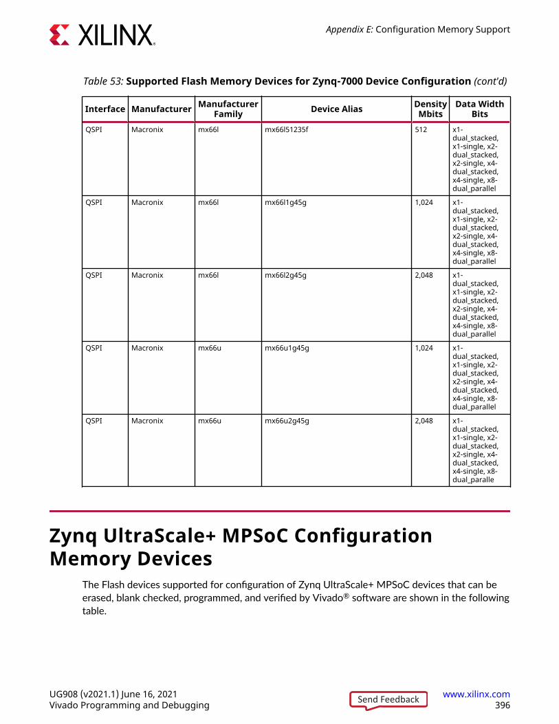
Table 53: Supported Flash Memory Devices for Zynq-7000 Device Configuration (cont'd)
Interface Manufacturer ManufacturerFamily Device Alias Density
MbitsData Width
BitsQSPI Macronix mx66l mx66l51235f 512 x1-
dual_stacked,x1-single, x2-dual_stacked,x2-single, x4-dual_stacked,x4-single, x8-dual_parallel
QSPI Macronix mx66l mx66l1g45g 1,024 x1-dual_stacked,x1-single, x2-dual_stacked,x2-single, x4-dual_stacked,x4-single, x8-dual_parallel
QSPI Macronix mx66l mx66l2g45g 2,048 x1-dual_stacked,x1-single, x2-dual_stacked,x2-single, x4-dual_stacked,x4-single, x8-dual_parallel
QSPI Macronix mx66u mx66u1g45g 1,024 x1-dual_stacked,x1-single, x2-dual_stacked,x2-single, x4-dual_stacked,x4-single, x8-dual_parallel
QSPI Macronix mx66u mx66u2g45g 2,048 x1-dual_stacked,x1-single, x2-dual_stacked,x2-single, x4-dual_stacked,x4-single, x8-dual_paralle
Zynq UltraScale+ MPSoC ConfigurationMemory Devices
The Flash devices supported for configuration of Zynq UltraScale+ MPSoC devices that can beerased, blank checked, programmed, and verified by Vivado® software are shown in the followingtable.
Appendix E: Configuration Memory Support
UG908 (v2021.1) June 16, 2021 www.xilinx.comVivado Programming and Debugging 396Send Feedback
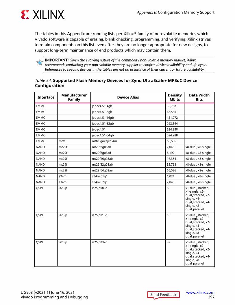
The tables in this Appendix are running lists per Xilinx® family of non-volatile memories whichVivado software is capable of erasing, blank checking, programming, and verifying. Xilinx strivesto retain components on this list even after they are no longer appropriate for new designs, tosupport long-term maintenance of end products which may contain them.
IMPORTANT! Given the evolving nature of the commodity non-volatile memory market, Xilinxrecommends contacting your non-volatile memory supplier to confirm device availability and life cycle.References to specific devices in the tables are not an assurance of their current or future availability.
Table 54: Supported Flash Memory Devices for Zynq UltraScale+ MPSoC DeviceConfiguration
Interface ManufacturerFamily Device Alias Density
MbitsData Width
BitsEMMC jedec4.51-4gb 32,768
EMMC jedec4.51-8gb 65,536
EMMC jedec4.51-16gb 131,072
EMMC jedec4.51-32gb 262,144
EMMC jedec4.51 524,288
EMMC jedec4.51-64gb 524,288
EMMC mtfc mtfc8gakajcn-4m 65,536
NAND mt29f mt29f2g08ab 2,048 x8-dual, x8-single
NAND mt29f mt29f8g08ad 8,192 x8-dual, x8-single
NAND mt29f mt29f16g08ab 16,384 x8-dual, x8-single
NAND mt29f mt29f32g08ab 32,768 x8-dual, x8-single
NAND mt29f mt29f64g08ae 65,536 x8-dual, x8-single
NAND s34ml s34ml01g1 1,024 x8-dual, x8-single
NAND s34ml s34ml02g1 2,048 x8-dual, x8-single
QSPI is25lp is25lp080d 8 x1-dual_stacked,x1-single, x2-dual_stacked, x2-single, x4-dual_stacked, x4-single, x8-dual_parallel
QSPI is25lp is25lp016d 16 x1-dual_stacked,x1-single, x2-dual_stacked, x2-single, x4-dual_stacked, x4-single, x8-dual_parallel
QSPI is25lp is25lp032d 32 x1-dual_stacked,x1-single, x2-dual_stacked, x2-single, x4-dual_stacked, x4-single, x8-dual_parallel
Appendix E: Configuration Memory Support
UG908 (v2021.1) June 16, 2021 www.xilinx.comVivado Programming and Debugging 397Send Feedback
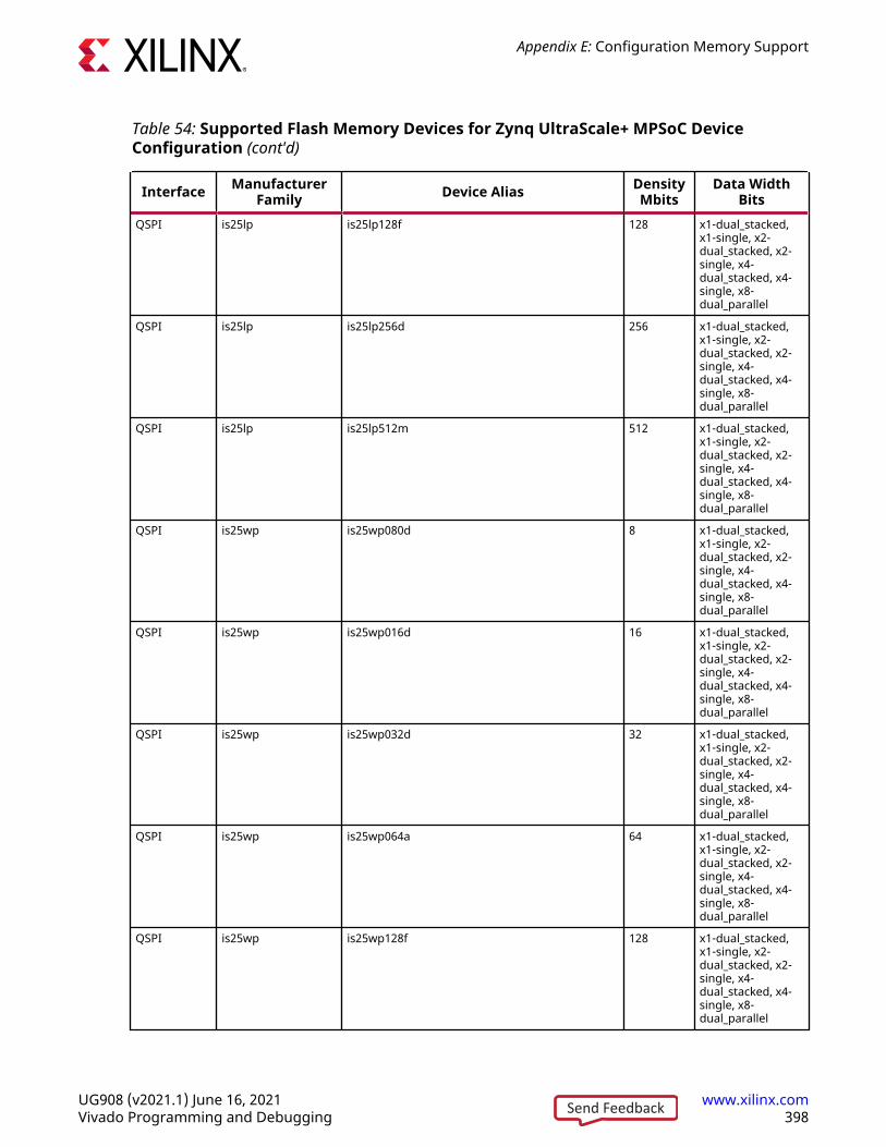
Table 54: Supported Flash Memory Devices for Zynq UltraScale+ MPSoC DeviceConfiguration (cont'd)
Interface ManufacturerFamily Device Alias Density
MbitsData Width
BitsQSPI is25lp is25lp128f 128 x1-dual_stacked,
x1-single, x2-dual_stacked, x2-single, x4-dual_stacked, x4-single, x8-dual_parallel
QSPI is25lp is25lp256d 256 x1-dual_stacked,x1-single, x2-dual_stacked, x2-single, x4-dual_stacked, x4-single, x8-dual_parallel
QSPI is25lp is25lp512m 512 x1-dual_stacked,x1-single, x2-dual_stacked, x2-single, x4-dual_stacked, x4-single, x8-dual_parallel
QSPI is25wp is25wp080d 8 x1-dual_stacked,x1-single, x2-dual_stacked, x2-single, x4-dual_stacked, x4-single, x8-dual_parallel
QSPI is25wp is25wp016d 16 x1-dual_stacked,x1-single, x2-dual_stacked, x2-single, x4-dual_stacked, x4-single, x8-dual_parallel
QSPI is25wp is25wp032d 32 x1-dual_stacked,x1-single, x2-dual_stacked, x2-single, x4-dual_stacked, x4-single, x8-dual_parallel
QSPI is25wp is25wp064a 64 x1-dual_stacked,x1-single, x2-dual_stacked, x2-single, x4-dual_stacked, x4-single, x8-dual_parallel
QSPI is25wp is25wp128f 128 x1-dual_stacked,x1-single, x2-dual_stacked, x2-single, x4-dual_stacked, x4-single, x8-dual_parallel
Appendix E: Configuration Memory Support
UG908 (v2021.1) June 16, 2021 www.xilinx.comVivado Programming and Debugging 398Send Feedback
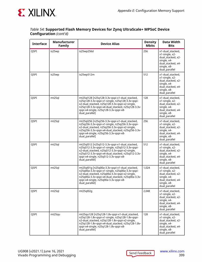
Table 54: Supported Flash Memory Devices for Zynq UltraScale+ MPSoC DeviceConfiguration (cont'd)
Interface ManufacturerFamily Device Alias Density
MbitsData Width
BitsQSPI is25wp is25wp256d 256 x1-dual_stacked,
x1-single, x2-dual_stacked, x2-single, x4-dual_stacked, x4-single, x8-dual_parallel
QSPI is25wp is25wp512m 512 x1-dual_stacked,x1-single, x2-dual_stacked, x2-single, x4-dual_stacked, x4-single, x8-dual_parallel
QSPI mt25ql mt25ql128 [n25q128-3.3v-qspi-x1-dual_stacked,n25q128-3.3v-qspi-x1-single, n25q128-3.3v-qspi-x2-dual_stacked, n25q128-3.3v-qspi-x2-single,n25q128-3.3v-qspi-x4-dual_stacked, n25q128-3.3v-qspi-x4-single, n25q128-3.3v-qspi-x8-dual_parallel]
128 x1-dual_stacked,x1-single, x2-dual_stacked, x2-single, x4-dual_stacked, x4-single, x8-dual_parallel
QSPI mt25ql mt25ql256 [n25q256-3.3v-qspi-x1-dual_stacked,n25q256-3.3v-qspi-x1-single, n25q256-3.3v-qspi-x2-dual_stacked, n25q256-3.3v-qspi-x2-single,n25q256-3.3v-qspi-x4-dual_stacked, n25q256-3.3v-qspi-x4-single, n25q256-3.3v-qspi-x8-dual_parallel]
256 x1-dual_stacked,x1-single, x2-dual_stacked, x2-single, x4-dual_stacked, x4-single, x8-dual_parallel
QSPI mt25ql mt25ql512 [n25q512-3.3v-qspi-x1-dual_stacked,n25q512-3.3v-qspi-x1-single, n25q512-3.3v-qspi-x2-dual_stacked, n25q512-3.3v-qspi-x2-single,n25q512-3.3v-qspi-x4-dual_stacked, n25q512-3.3v-qspi-x4-single, n25q512-3.3v-qspi-x8-dual_parallel]
512 x1-dual_stacked,x1-single, x2-dual_stacked, x2-single, x4-dual_stacked, x4-single, x8-dual_parallel
QSPI mt25ql mt25ql01g [n25q00a-3.3v-qspi-x1-dual_stacked,n25q00a-3.3v-qspi-x1-single, n25q00a-3.3v-qspi-x2-dual_stacked, n25q00a-3.3v-qspi-x2-single,n25q00a-3.3v-qspi-x4-dual_stacked, n25q00a-3.3v-qspi-x4-single, n25q00a-3.3v-qspi-x8-dual_parallel]
1,024 x1-dual_stacked,x1-single, x2-dual_stacked, x2-single, x4-dual_stacked, x4-single, x8-dual_parallel
QSPI mt25ql mt25ql02g 2,048 x1-dual_stacked,x1-single, x2-dual_stacked, x2-single, x4-dual_stacked, x4-single, x8-dual_parallel
QSPI mt25qu mt25qu128 [n25q128-1.8v-qspi-x1-dual_stacked,n25q128-1.8v-qspi-x1-single, n25q128-1.8v-qspi-x2-dual_stacked, n25q128-1.8v-qspi-x2-single,n25q128-1.8v-qspi-x4-dual_stacked, n25q128-1.8v-qspi-x4-single, n25q128-1.8v-qspi-x8-dual_parallel]
128 x1-dual_stacked,x1-single, x2-dual_stacked, x2-single, x4-dual_stacked, x4-single, x8-dual_parallel
Appendix E: Configuration Memory Support
UG908 (v2021.1) June 16, 2021 www.xilinx.comVivado Programming and Debugging 399Send Feedback
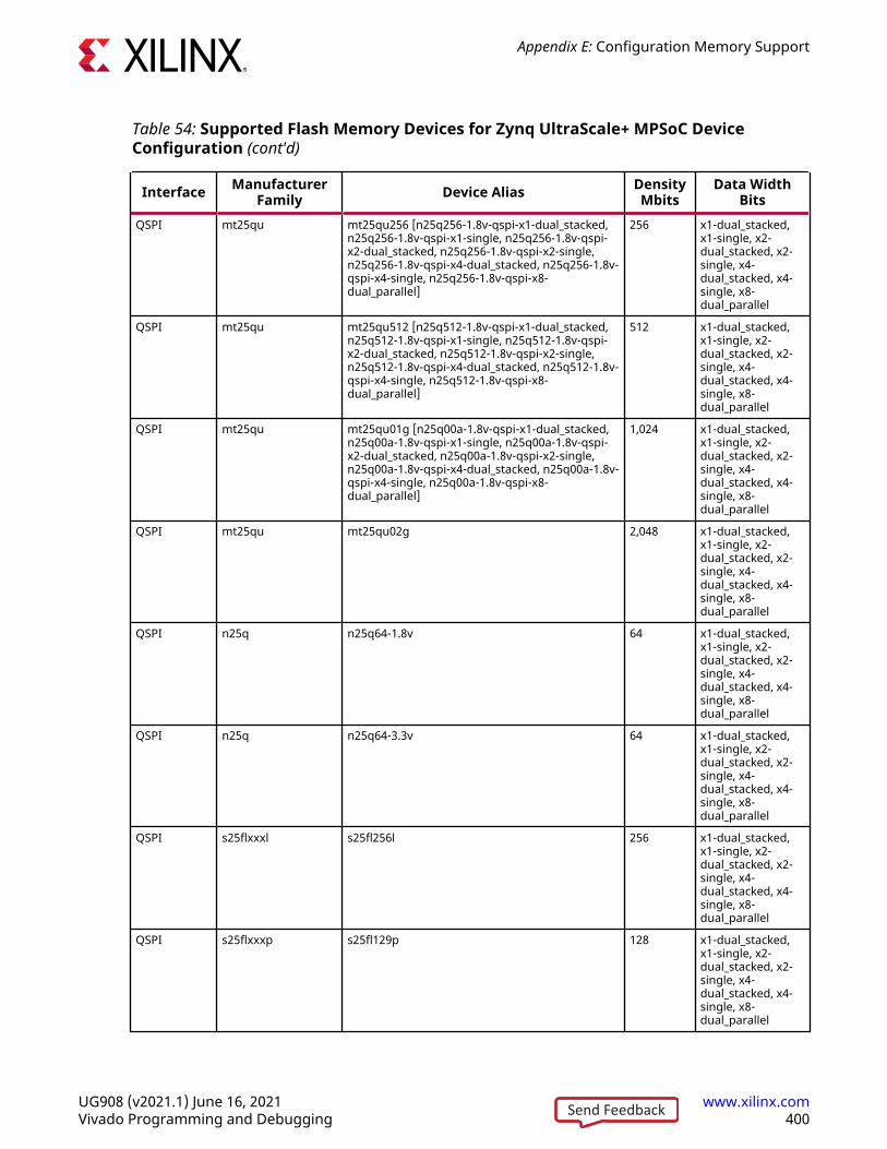
Table 54: Supported Flash Memory Devices for Zynq UltraScale+ MPSoC DeviceConfiguration (cont'd)
Interface ManufacturerFamily Device Alias Density
MbitsData Width
BitsQSPI mt25qu mt25qu256 [n25q256-1.8v-qspi-x1-dual_stacked,
n25q256-1.8v-qspi-x1-single, n25q256-1.8v-qspi-x2-dual_stacked, n25q256-1.8v-qspi-x2-single,n25q256-1.8v-qspi-x4-dual_stacked, n25q256-1.8v-qspi-x4-single, n25q256-1.8v-qspi-x8-dual_parallel]
256 x1-dual_stacked,x1-single, x2-dual_stacked, x2-single, x4-dual_stacked, x4-single, x8-dual_parallel
QSPI mt25qu mt25qu512 [n25q512-1.8v-qspi-x1-dual_stacked,n25q512-1.8v-qspi-x1-single, n25q512-1.8v-qspi-x2-dual_stacked, n25q512-1.8v-qspi-x2-single,n25q512-1.8v-qspi-x4-dual_stacked, n25q512-1.8v-qspi-x4-single, n25q512-1.8v-qspi-x8-dual_parallel]
512 x1-dual_stacked,x1-single, x2-dual_stacked, x2-single, x4-dual_stacked, x4-single, x8-dual_parallel
QSPI mt25qu mt25qu01g [n25q00a-1.8v-qspi-x1-dual_stacked,n25q00a-1.8v-qspi-x1-single, n25q00a-1.8v-qspi-x2-dual_stacked, n25q00a-1.8v-qspi-x2-single,n25q00a-1.8v-qspi-x4-dual_stacked, n25q00a-1.8v-qspi-x4-single, n25q00a-1.8v-qspi-x8-dual_parallel]
1,024 x1-dual_stacked,x1-single, x2-dual_stacked, x2-single, x4-dual_stacked, x4-single, x8-dual_parallel
QSPI mt25qu mt25qu02g 2,048 x1-dual_stacked,x1-single, x2-dual_stacked, x2-single, x4-dual_stacked, x4-single, x8-dual_parallel
QSPI n25q n25q64-1.8v 64 x1-dual_stacked,x1-single, x2-dual_stacked, x2-single, x4-dual_stacked, x4-single, x8-dual_parallel
QSPI n25q n25q64-3.3v 64 x1-dual_stacked,x1-single, x2-dual_stacked, x2-single, x4-dual_stacked, x4-single, x8-dual_parallel
QSPI s25flxxxl s25fl256l 256 x1-dual_stacked,x1-single, x2-dual_stacked, x2-single, x4-dual_stacked, x4-single, x8-dual_parallel
QSPI s25flxxxp s25fl129p 128 x1-dual_stacked,x1-single, x2-dual_stacked, x2-single, x4-dual_stacked, x4-single, x8-dual_parallel
Appendix E: Configuration Memory Support
UG908 (v2021.1) June 16, 2021 www.xilinx.comVivado Programming and Debugging 400Send Feedback
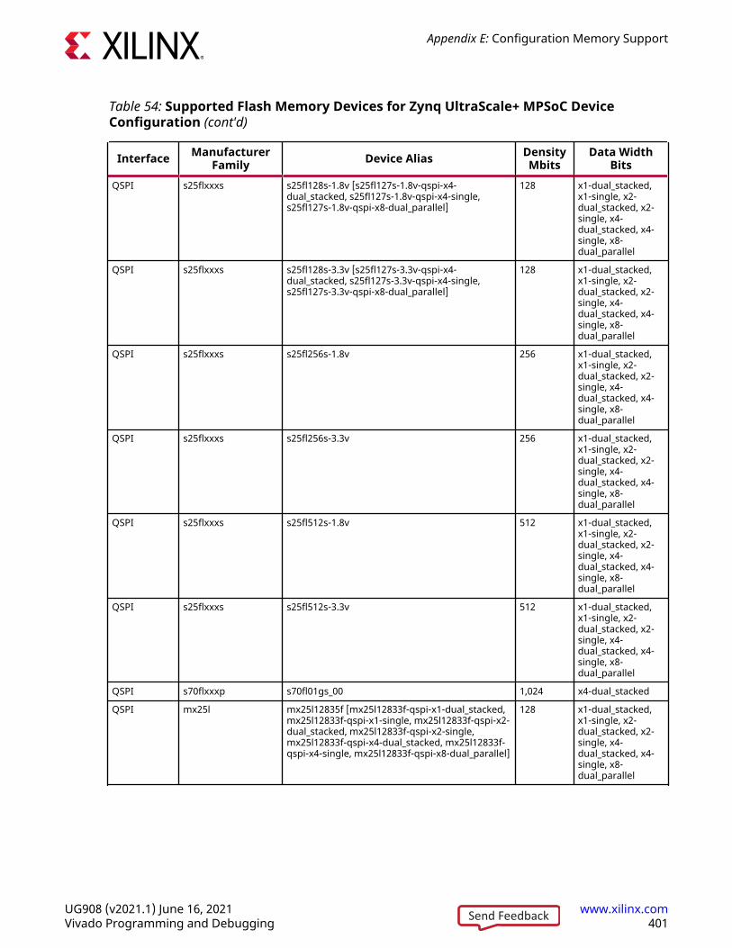
Table 54: Supported Flash Memory Devices for Zynq UltraScale+ MPSoC DeviceConfiguration (cont'd)
Interface ManufacturerFamily Device Alias Density
MbitsData Width
BitsQSPI s25flxxxs s25fl128s-1.8v [s25fl127s-1.8v-qspi-x4-
dual_stacked, s25fl127s-1.8v-qspi-x4-single,s25fl127s-1.8v-qspi-x8-dual_parallel]
128 x1-dual_stacked,x1-single, x2-dual_stacked, x2-single, x4-dual_stacked, x4-single, x8-dual_parallel
QSPI s25flxxxs s25fl128s-3.3v [s25fl127s-3.3v-qspi-x4-dual_stacked, s25fl127s-3.3v-qspi-x4-single,s25fl127s-3.3v-qspi-x8-dual_parallel]
128 x1-dual_stacked,x1-single, x2-dual_stacked, x2-single, x4-dual_stacked, x4-single, x8-dual_parallel
QSPI s25flxxxs s25fl256s-1.8v 256 x1-dual_stacked,x1-single, x2-dual_stacked, x2-single, x4-dual_stacked, x4-single, x8-dual_parallel
QSPI s25flxxxs s25fl256s-3.3v 256 x1-dual_stacked,x1-single, x2-dual_stacked, x2-single, x4-dual_stacked, x4-single, x8-dual_parallel
QSPI s25flxxxs s25fl512s-1.8v 512 x1-dual_stacked,x1-single, x2-dual_stacked, x2-single, x4-dual_stacked, x4-single, x8-dual_parallel
QSPI s25flxxxs s25fl512s-3.3v 512 x1-dual_stacked,x1-single, x2-dual_stacked, x2-single, x4-dual_stacked, x4-single, x8-dual_parallel
QSPI s70flxxxp s70fl01gs_00 1,024 x4-dual_stacked
QSPI mx25l mx25l12835f [mx25l12833f-qspi-x1-dual_stacked,mx25l12833f-qspi-x1-single, mx25l12833f-qspi-x2-dual_stacked, mx25l12833f-qspi-x2-single,mx25l12833f-qspi-x4-dual_stacked, mx25l12833f-qspi-x4-single, mx25l12833f-qspi-x8-dual_parallel]
128 x1-dual_stacked,x1-single, x2-dual_stacked, x2-single, x4-dual_stacked, x4-single, x8-dual_parallel
Appendix E: Configuration Memory Support
UG908 (v2021.1) June 16, 2021 www.xilinx.comVivado Programming and Debugging 401Send Feedback
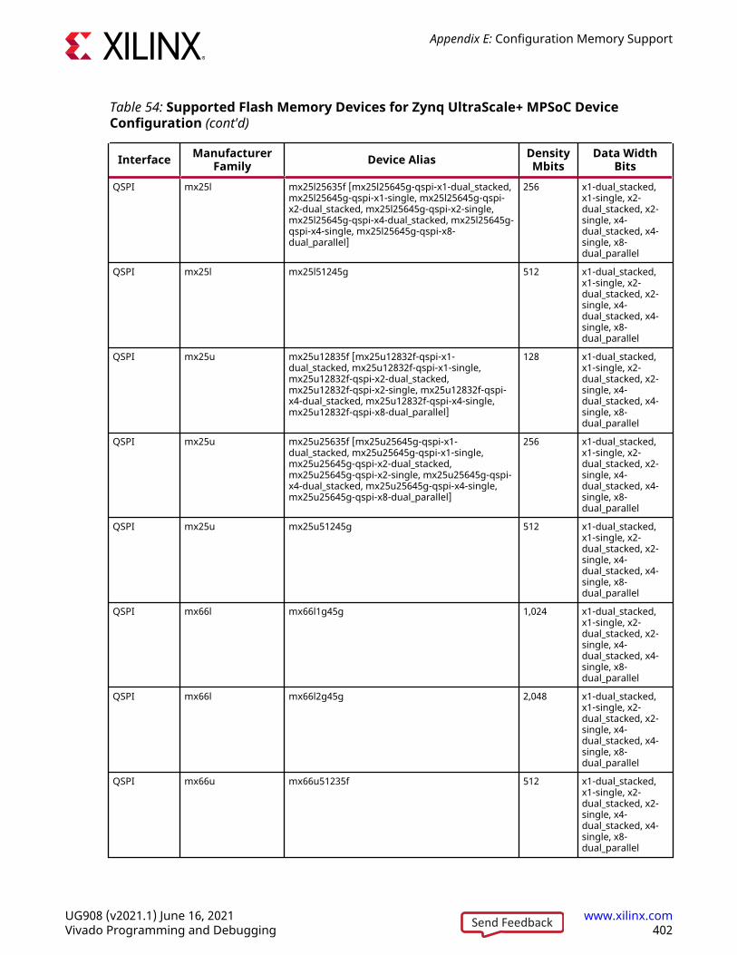
Table 54: Supported Flash Memory Devices for Zynq UltraScale+ MPSoC DeviceConfiguration (cont'd)
Interface ManufacturerFamily Device Alias Density
MbitsData Width
BitsQSPI mx25l mx25l25635f [mx25l25645g-qspi-x1-dual_stacked,
mx25l25645g-qspi-x1-single, mx25l25645g-qspi-x2-dual_stacked, mx25l25645g-qspi-x2-single,mx25l25645g-qspi-x4-dual_stacked, mx25l25645g-qspi-x4-single, mx25l25645g-qspi-x8-dual_parallel]
256 x1-dual_stacked,x1-single, x2-dual_stacked, x2-single, x4-dual_stacked, x4-single, x8-dual_parallel
QSPI mx25l mx25l51245g 512 x1-dual_stacked,x1-single, x2-dual_stacked, x2-single, x4-dual_stacked, x4-single, x8-dual_parallel
QSPI mx25u mx25u12835f [mx25u12832f-qspi-x1-dual_stacked, mx25u12832f-qspi-x1-single,mx25u12832f-qspi-x2-dual_stacked,mx25u12832f-qspi-x2-single, mx25u12832f-qspi-x4-dual_stacked, mx25u12832f-qspi-x4-single,mx25u12832f-qspi-x8-dual_parallel]
128 x1-dual_stacked,x1-single, x2-dual_stacked, x2-single, x4-dual_stacked, x4-single, x8-dual_parallel
QSPI mx25u mx25u25635f [mx25u25645g-qspi-x1-dual_stacked, mx25u25645g-qspi-x1-single,mx25u25645g-qspi-x2-dual_stacked,mx25u25645g-qspi-x2-single, mx25u25645g-qspi-x4-dual_stacked, mx25u25645g-qspi-x4-single,mx25u25645g-qspi-x8-dual_parallel]
256 x1-dual_stacked,x1-single, x2-dual_stacked, x2-single, x4-dual_stacked, x4-single, x8-dual_parallel
QSPI mx25u mx25u51245g 512 x1-dual_stacked,x1-single, x2-dual_stacked, x2-single, x4-dual_stacked, x4-single, x8-dual_parallel
QSPI mx66l mx66l1g45g 1,024 x1-dual_stacked,x1-single, x2-dual_stacked, x2-single, x4-dual_stacked, x4-single, x8-dual_parallel
QSPI mx66l mx66l2g45g 2,048 x1-dual_stacked,x1-single, x2-dual_stacked, x2-single, x4-dual_stacked, x4-single, x8-dual_parallel
QSPI mx66u mx66u51235f 512 x1-dual_stacked,x1-single, x2-dual_stacked, x2-single, x4-dual_stacked, x4-single, x8-dual_parallel
Appendix E: Configuration Memory Support
UG908 (v2021.1) June 16, 2021 www.xilinx.comVivado Programming and Debugging 402Send Feedback
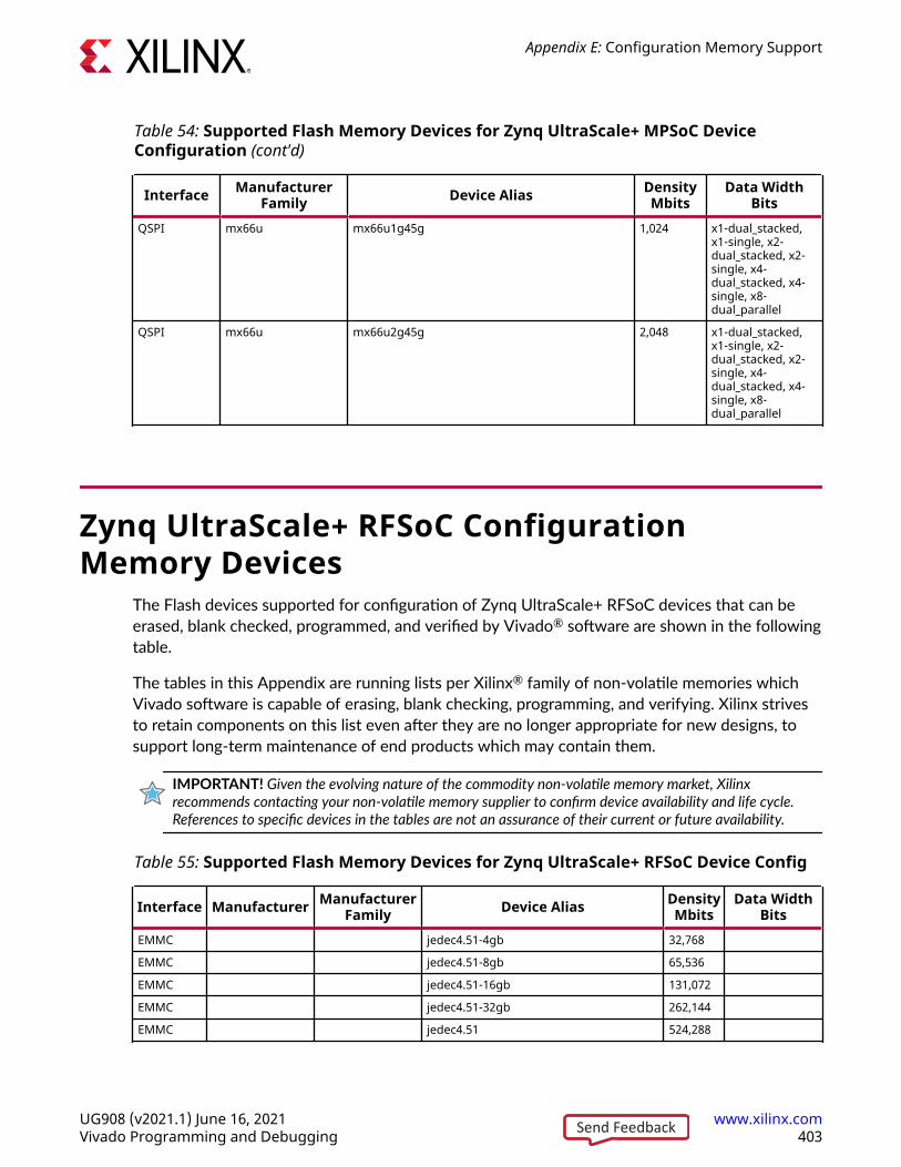
Table 54: Supported Flash Memory Devices for Zynq UltraScale+ MPSoC DeviceConfiguration (cont'd)
Interface ManufacturerFamily Device Alias Density
MbitsData Width
BitsQSPI mx66u mx66u1g45g 1,024 x1-dual_stacked,
x1-single, x2-dual_stacked, x2-single, x4-dual_stacked, x4-single, x8-dual_parallel
QSPI mx66u mx66u2g45g 2,048 x1-dual_stacked,x1-single, x2-dual_stacked, x2-single, x4-dual_stacked, x4-single, x8-dual_parallel
Zynq UltraScale+ RFSoC ConfigurationMemory Devices
The Flash devices supported for configuration of Zynq UltraScale+ RFSoC devices that can beerased, blank checked, programmed, and verified by Vivado® software are shown in the followingtable.
The tables in this Appendix are running lists per Xilinx® family of non-volatile memories whichVivado software is capable of erasing, blank checking, programming, and verifying. Xilinx strivesto retain components on this list even after they are no longer appropriate for new designs, tosupport long-term maintenance of end products which may contain them.
IMPORTANT! Given the evolving nature of the commodity non-volatile memory market, Xilinxrecommends contacting your non-volatile memory supplier to confirm device availability and life cycle.References to specific devices in the tables are not an assurance of their current or future availability.
Table 55: Supported Flash Memory Devices for Zynq UltraScale+ RFSoC Device Config
Interface Manufacturer ManufacturerFamily Device Alias Density
MbitsData Width
BitsEMMC jedec4.51-4gb 32,768
EMMC jedec4.51-8gb 65,536
EMMC jedec4.51-16gb 131,072
EMMC jedec4.51-32gb 262,144
EMMC jedec4.51 524,288
Appendix E: Configuration Memory Support
UG908 (v2021.1) June 16, 2021 www.xilinx.comVivado Programming and Debugging 403Send Feedback
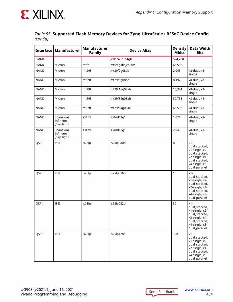
Table 55: Supported Flash Memory Devices for Zynq UltraScale+ RFSoC Device Config(cont'd)
Interface Manufacturer ManufacturerFamily Device Alias Density
MbitsData Width
BitsEMMC jedec4.51-64gb 524,288
EMMC Micron mtfc mtfc8gakajcn-4m 65,536
NAND Micron mt29f mt29f2g08ab 2,048 x8-dual, x8-single
NAND Micron mt29f mt29f8g08ad 8,192 x8-dual, x8-single
NAND Micron mt29f mt29f16g08ab 16,384 x8-dual, x8-single
NAND Micron mt29f mt29f32g08ab 32,768 x8-dual, x8-single
NAND Micron mt29f mt29f64g08ae 65,536 x8-dual, x8-single
NAND Spansion/Infineon(SkyHigh)
s34ml s34ml01g1 1,024 x8-dual, x8-single
NAND Spansion/Infineon(SkyHigh)
s34ml s34ml02g1 2,048 x8-dual, x8-single
QSPI ISSI is25lp is25lp080d 8 x1-dual_stacked,x1-single, x2-dual_stacked,x2-single, x4-dual_stacked,x4-single, x8-dual_parallel
QSPI ISSI is25lp is25lp016d 16 x1-dual_stacked,x1-single, x2-dual_stacked,x2-single, x4-dual_stacked,x4-single, x8-dual_parallel
QSPI ISSI is25lp is25lp032d 32 x1-dual_stacked,x1-single, x2-dual_stacked,x2-single, x4-dual_stacked,x4-single, x8-dual_parallel
QSPI ISSI is25lp is25lp128f 128 x1-dual_stacked,x1-single, x2-dual_stacked,x2-single, x4-dual_stacked,x4-single, x8-dual_parallel
Appendix E: Configuration Memory Support
UG908 (v2021.1) June 16, 2021 www.xilinx.comVivado Programming and Debugging 404Send Feedback
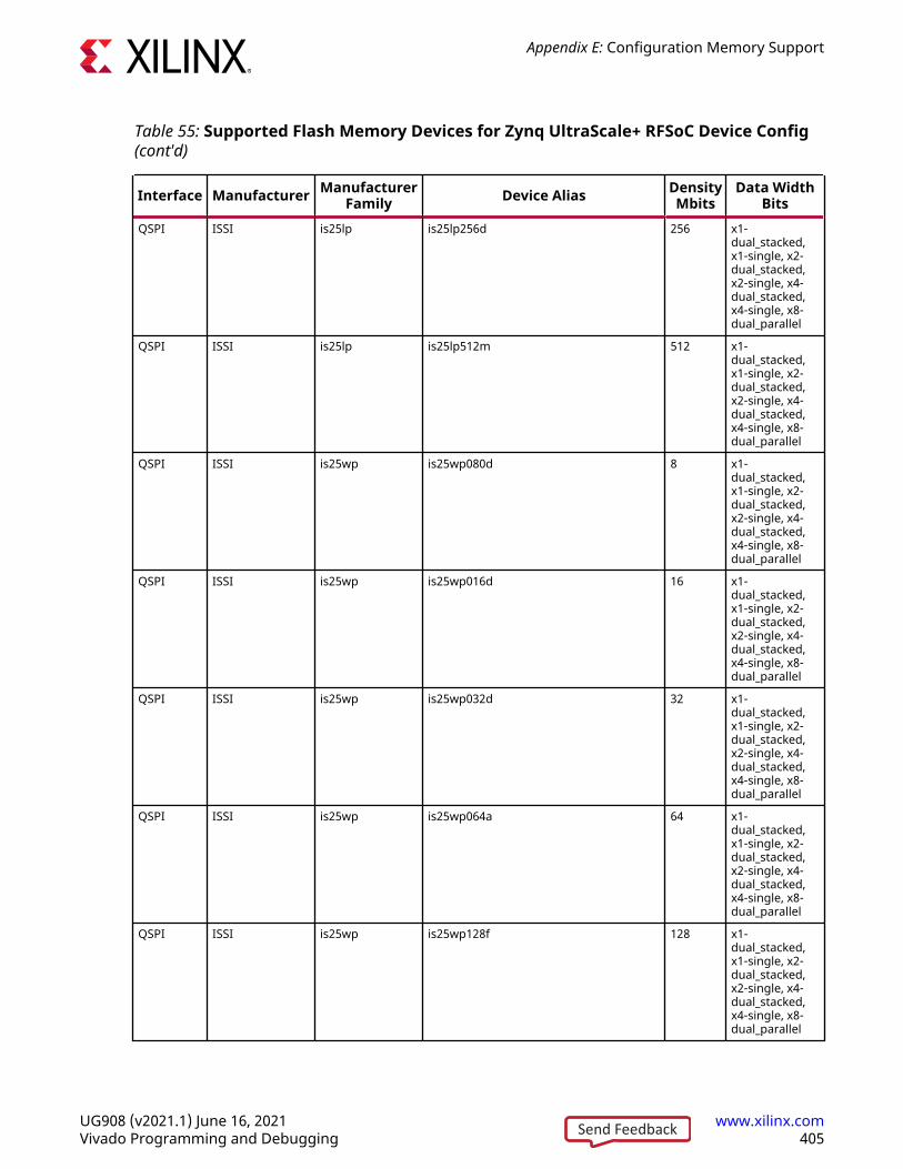
Table 55: Supported Flash Memory Devices for Zynq UltraScale+ RFSoC Device Config(cont'd)
Interface Manufacturer ManufacturerFamily Device Alias Density
MbitsData Width
BitsQSPI ISSI is25lp is25lp256d 256 x1-
dual_stacked,x1-single, x2-dual_stacked,x2-single, x4-dual_stacked,x4-single, x8-dual_parallel
QSPI ISSI is25lp is25lp512m 512 x1-dual_stacked,x1-single, x2-dual_stacked,x2-single, x4-dual_stacked,x4-single, x8-dual_parallel
QSPI ISSI is25wp is25wp080d 8 x1-dual_stacked,x1-single, x2-dual_stacked,x2-single, x4-dual_stacked,x4-single, x8-dual_parallel
QSPI ISSI is25wp is25wp016d 16 x1-dual_stacked,x1-single, x2-dual_stacked,x2-single, x4-dual_stacked,x4-single, x8-dual_parallel
QSPI ISSI is25wp is25wp032d 32 x1-dual_stacked,x1-single, x2-dual_stacked,x2-single, x4-dual_stacked,x4-single, x8-dual_parallel
QSPI ISSI is25wp is25wp064a 64 x1-dual_stacked,x1-single, x2-dual_stacked,x2-single, x4-dual_stacked,x4-single, x8-dual_parallel
QSPI ISSI is25wp is25wp128f 128 x1-dual_stacked,x1-single, x2-dual_stacked,x2-single, x4-dual_stacked,x4-single, x8-dual_parallel
Appendix E: Configuration Memory Support
UG908 (v2021.1) June 16, 2021 www.xilinx.comVivado Programming and Debugging 405Send Feedback
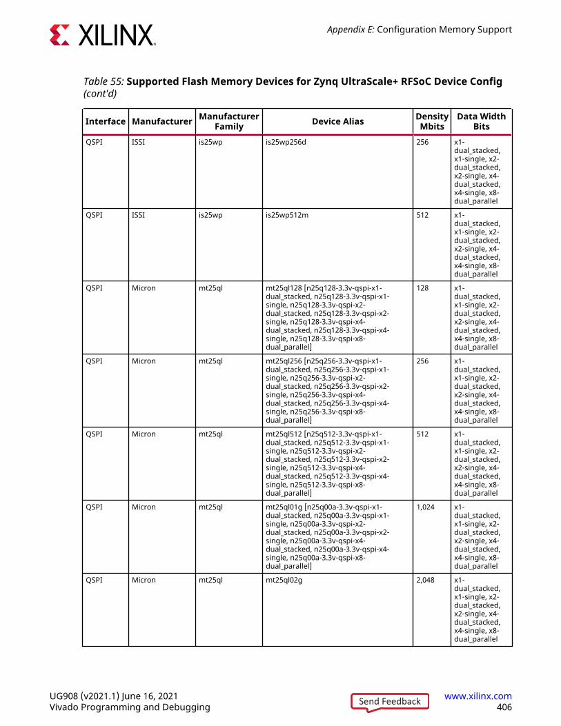
Table 55: Supported Flash Memory Devices for Zynq UltraScale+ RFSoC Device Config(cont'd)
Interface Manufacturer ManufacturerFamily Device Alias Density
MbitsData Width
BitsQSPI ISSI is25wp is25wp256d 256 x1-
dual_stacked,x1-single, x2-dual_stacked,x2-single, x4-dual_stacked,x4-single, x8-dual_parallel
QSPI ISSI is25wp is25wp512m 512 x1-dual_stacked,x1-single, x2-dual_stacked,x2-single, x4-dual_stacked,x4-single, x8-dual_parallel
QSPI Micron mt25ql mt25ql128 [n25q128-3.3v-qspi-x1-dual_stacked, n25q128-3.3v-qspi-x1-single, n25q128-3.3v-qspi-x2-dual_stacked, n25q128-3.3v-qspi-x2-single, n25q128-3.3v-qspi-x4-dual_stacked, n25q128-3.3v-qspi-x4-single, n25q128-3.3v-qspi-x8-dual_parallel]
128 x1-dual_stacked,x1-single, x2-dual_stacked,x2-single, x4-dual_stacked,x4-single, x8-dual_parallel
QSPI Micron mt25ql mt25ql256 [n25q256-3.3v-qspi-x1-dual_stacked, n25q256-3.3v-qspi-x1-single, n25q256-3.3v-qspi-x2-dual_stacked, n25q256-3.3v-qspi-x2-single, n25q256-3.3v-qspi-x4-dual_stacked, n25q256-3.3v-qspi-x4-single, n25q256-3.3v-qspi-x8-dual_parallel]
256 x1-dual_stacked,x1-single, x2-dual_stacked,x2-single, x4-dual_stacked,x4-single, x8-dual_parallel
QSPI Micron mt25ql mt25ql512 [n25q512-3.3v-qspi-x1-dual_stacked, n25q512-3.3v-qspi-x1-single, n25q512-3.3v-qspi-x2-dual_stacked, n25q512-3.3v-qspi-x2-single, n25q512-3.3v-qspi-x4-dual_stacked, n25q512-3.3v-qspi-x4-single, n25q512-3.3v-qspi-x8-dual_parallel]
512 x1-dual_stacked,x1-single, x2-dual_stacked,x2-single, x4-dual_stacked,x4-single, x8-dual_parallel
QSPI Micron mt25ql mt25ql01g [n25q00a-3.3v-qspi-x1-dual_stacked, n25q00a-3.3v-qspi-x1-single, n25q00a-3.3v-qspi-x2-dual_stacked, n25q00a-3.3v-qspi-x2-single, n25q00a-3.3v-qspi-x4-dual_stacked, n25q00a-3.3v-qspi-x4-single, n25q00a-3.3v-qspi-x8-dual_parallel]
1,024 x1-dual_stacked,x1-single, x2-dual_stacked,x2-single, x4-dual_stacked,x4-single, x8-dual_parallel
QSPI Micron mt25ql mt25ql02g 2,048 x1-dual_stacked,x1-single, x2-dual_stacked,x2-single, x4-dual_stacked,x4-single, x8-dual_parallel
Appendix E: Configuration Memory Support
UG908 (v2021.1) June 16, 2021 www.xilinx.comVivado Programming and Debugging 406Send Feedback
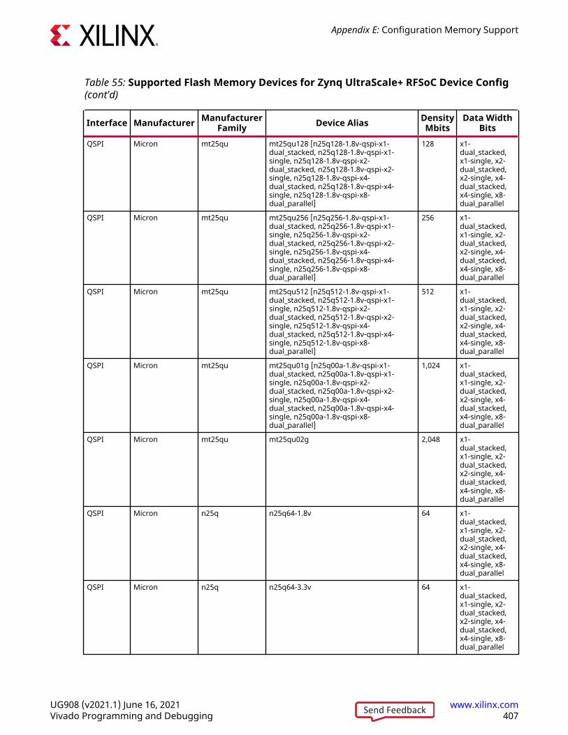
Table 55: Supported Flash Memory Devices for Zynq UltraScale+ RFSoC Device Config(cont'd)
Interface Manufacturer ManufacturerFamily Device Alias Density
MbitsData Width
BitsQSPI Micron mt25qu mt25qu128 [n25q128-1.8v-qspi-x1-
dual_stacked, n25q128-1.8v-qspi-x1-single, n25q128-1.8v-qspi-x2-dual_stacked, n25q128-1.8v-qspi-x2-single, n25q128-1.8v-qspi-x4-dual_stacked, n25q128-1.8v-qspi-x4-single, n25q128-1.8v-qspi-x8-dual_parallel]
128 x1-dual_stacked,x1-single, x2-dual_stacked,x2-single, x4-dual_stacked,x4-single, x8-dual_parallel
QSPI Micron mt25qu mt25qu256 [n25q256-1.8v-qspi-x1-dual_stacked, n25q256-1.8v-qspi-x1-single, n25q256-1.8v-qspi-x2-dual_stacked, n25q256-1.8v-qspi-x2-single, n25q256-1.8v-qspi-x4-dual_stacked, n25q256-1.8v-qspi-x4-single, n25q256-1.8v-qspi-x8-dual_parallel]
256 x1-dual_stacked,x1-single, x2-dual_stacked,x2-single, x4-dual_stacked,x4-single, x8-dual_parallel
QSPI Micron mt25qu mt25qu512 [n25q512-1.8v-qspi-x1-dual_stacked, n25q512-1.8v-qspi-x1-single, n25q512-1.8v-qspi-x2-dual_stacked, n25q512-1.8v-qspi-x2-single, n25q512-1.8v-qspi-x4-dual_stacked, n25q512-1.8v-qspi-x4-single, n25q512-1.8v-qspi-x8-dual_parallel]
512 x1-dual_stacked,x1-single, x2-dual_stacked,x2-single, x4-dual_stacked,x4-single, x8-dual_parallel
QSPI Micron mt25qu mt25qu01g [n25q00a-1.8v-qspi-x1-dual_stacked, n25q00a-1.8v-qspi-x1-single, n25q00a-1.8v-qspi-x2-dual_stacked, n25q00a-1.8v-qspi-x2-single, n25q00a-1.8v-qspi-x4-dual_stacked, n25q00a-1.8v-qspi-x4-single, n25q00a-1.8v-qspi-x8-dual_parallel]
1,024 x1-dual_stacked,x1-single, x2-dual_stacked,x2-single, x4-dual_stacked,x4-single, x8-dual_parallel
QSPI Micron mt25qu mt25qu02g 2,048 x1-dual_stacked,x1-single, x2-dual_stacked,x2-single, x4-dual_stacked,x4-single, x8-dual_parallel
QSPI Micron n25q n25q64-1.8v 64 x1-dual_stacked,x1-single, x2-dual_stacked,x2-single, x4-dual_stacked,x4-single, x8-dual_parallel
QSPI Micron n25q n25q64-3.3v 64 x1-dual_stacked,x1-single, x2-dual_stacked,x2-single, x4-dual_stacked,x4-single, x8-dual_parallel
Appendix E: Configuration Memory Support
UG908 (v2021.1) June 16, 2021 www.xilinx.comVivado Programming and Debugging 407Send Feedback
Table 55: Supported Flash Memory Devices for Zynq UltraScale+ RFSoC Device Config(cont'd)
Interface Manufacturer ManufacturerFamily Device Alias Density
MbitsData Width
BitsQSPI Spansion/
Infineons25flxxxl s25fl256l 256 x1-
dual_stacked,x1-single, x2-dual_stacked,x2-single, x4-dual_stacked,x4-single, x8-dual_parallel
QSPI Spansion/Infineon
s25flxxxp s25fl129p 128 x1-dual_stacked,x1-single, x2-dual_stacked,x2-single, x4-dual_stacked,x4-single, x8-dual_parallel
QSPI Spansion/Infineon
s25flxxxs s25fl128s-1.8v [s25fl127s-1.8v-qspi-x4-dual_stacked, s25fl127s-1.8v-qspi-x4-single, s25fl127s-1.8v-qspi-x8-dual_parallel]
128 x1-dual_stacked,x1-single, x2-dual_stacked,x2-single, x4-dual_stacked,x4-single, x8-dual_parallel
QSPI Spansion/Infineon
s25flxxxs s25fl128s-3.3v [s25fl127s-3.3v-qspi-x4-dual_stacked, s25fl127s-3.3v-qspi-x4-single, s25fl127s-3.3v-qspi-x8-dual_parallel]
128 x1-dual_stacked,x1-single, x2-dual_stacked,x2-single, x4-dual_stacked,x4-single, x8-dual_parallel
QSPI Spansion/Infineon
s25flxxxs s25fl256s-1.8v 256 x1-dual_stacked,x1-single, x2-dual_stacked,x2-single, x4-dual_stacked,x4-single, x8-dual_parallel
QSPI Spansion/Infineon
s25flxxxs s25fl256s-3.3v 256 x1-dual_stacked,x1-single, x2-dual_stacked,x2-single, x4-dual_stacked,x4-single, x8-dual_parallel
QSPI Spansion/Infineon
s25flxxxs s25fl512s-1.8v 512 x1-dual_stacked,x1-single, x2-dual_stacked,x2-single, x4-dual_stacked,x4-single, x8-dual_parallel
Appendix E: Configuration Memory Support
UG908 (v2021.1) June 16, 2021 www.xilinx.comVivado Programming and Debugging 408Send Feedback
Table 55: Supported Flash Memory Devices for Zynq UltraScale+ RFSoC Device Config(cont'd)
Interface Manufacturer ManufacturerFamily Device Alias Density
MbitsData Width
BitsQSPI Spansion/
Infineons25flxxxs s25fl512s-3.3v 512 x1-
dual_stacked,x1-single, x2-dual_stacked,x2-single, x4-dual_stacked,x4-single, x8-dual_parallel
QSPI Spansion/Infineon
s70flxxxp s70fl01gs_00 1,024 x4-dual_stacked
QSPI Macronix mx25l mx25l12835f [mx25l12833f-qspi-x1-dual_stacked, mx25l12833f-qspi-x1-single,mx25l12833f-qspi-x2-dual_stacked,mx25l12833f-qspi-x2-single, mx25l12833f-qspi-x4-dual_stacked, mx25l12833f-qspi-x4-single, mx25l12833f-qspi-x8-dual_parallel]
128 x1-dual_stacked,x1-single, x2-dual_stacked,x2-single, x4-dual_stacked,x4-single, x8-dual_parallel
QSPI Macronix mx25l mx25l25635f [mx25l25645g-qspi-x1-dual_stacked, mx25l25645g-qspi-x1-single, mx25l25645g-qspi-x2-dual_stacked, mx25l25645g-qspi-x2-single, mx25l25645g-qspi-x4-dual_stacked, mx25l25645g-qspi-x4-single, mx25l25645g-qspi-x8-dual_parallel]
256 x1-dual_stacked,x1-single, x2-dual_stacked,x2-single, x4-dual_stacked,x4-single, x8-dual_parallel
QSPI Macronix mx25l mx25l51245g 512 x1-dual_stacked,x1-single, x2-dual_stacked,x2-single, x4-dual_stacked,x4-single, x8-dual_parallel
QSPI Macronix mx25u mx25u12835f [mx25u12832f-qspi-x1-dual_stacked, mx25u12832f-qspi-x1-single, mx25u12832f-qspi-x2-dual_stacked, mx25u12832f-qspi-x2-single, mx25u12832f-qspi-x4-dual_stacked, mx25u12832f-qspi-x4-single, mx25u12832f-qspi-x8-dual_parallel]
128 x1-dual_stacked,x1-single, x2-dual_stacked,x2-single, x4-dual_stacked,x4-single, x8-dual_parallel
QSPI Macronix mx25u mx25u25635f [mx25u25645g-qspi-x1-dual_stacked, mx25u25645g-qspi-x1-single, mx25u25645g-qspi-x2-dual_stacked, mx25u25645g-qspi-x2-single, mx25u25645g-qspi-x4-dual_stacked, mx25u25645g-qspi-x4-single, mx25u25645g-qspi-x8-dual_parallel]
256 x1-dual_stacked,x1-single, x2-dual_stacked,x2-single, x4-dual_stacked,x4-single, x8-dual_parallel
Appendix E: Configuration Memory Support
UG908 (v2021.1) June 16, 2021 www.xilinx.comVivado Programming and Debugging 409Send Feedback
Table 55: Supported Flash Memory Devices for Zynq UltraScale+ RFSoC Device Config(cont'd)
Interface Manufacturer ManufacturerFamily Device Alias Density
MbitsData Width
BitsQSPI Macronix mx25u mx25u51245g 512 x1-
dual_stacked,x1-single, x2-dual_stacked,x2-single, x4-dual_stacked,x4-single, x8-dual_parallel
QSPI Macronix mx66l mx66l1g45g 1,024 x1-dual_stacked,x1-single, x2-dual_stacked,x2-single, x4-dual_stacked,x4-single, x8-dual_parallel
QSPI Macronix mx66l mx66l2g45g 2,048 x1-dual_stacked,x1-single, x2-dual_stacked,x2-single, x4-dual_stacked,x4-single, x8-dual_parallel
QSPI Macronix mx66u mx66u51235f 512 x1-dual_stacked,x1-single, x2-dual_stacked,x2-single, x4-dual_stacked,x4-single, x8-dual_parallel
QSPI Macronix mx66u mx66u1g45g 1,024 x1-dual_stacked,x1-single, x2-dual_stacked,x2-single, x4-dual_stacked,x4-single, x8-dual_parallel
QSPI Macronix mx66u mx66u2g45g 2,048 x1-dual_stacked,x1-single, x2-dual_stacked,x2-single, x4-dual_stacked,x4-single, x8-dual_parallel
Appendix E: Configuration Memory Support
UG908 (v2021.1) June 16, 2021 www.xilinx.comVivado Programming and Debugging 410Send Feedback
Versal Configuration Memory DevicesNote: For flash memory devices with official industry specifications, such as eMMC and SD, the devicesupport is based on compliance to specification versions, rather than by enumeration of specificmanufacturer, manufacturer family, and device part number. This provides designers with a wider range ofpossibilities in initial flash selection and long term design maintenance.
Note: When selecting QSPI or OSPI density, select the maximum, because the maximum density alsosupports lower density devices. For example, selecting 2 Gb density also supports lower density devicessuch as 1 Gb or 512 Mb. This is unlike previous architectures.
Table 56: Supported Flash Memory Devices for Versal Device Configuration
Interface Manufacturer ManufacturerFamily
DeviceName
VivadoSelection
Density(Mb)
Data Width(Bits)
EMMC jedec4.51-4gb
jedec4.51-4gb
32,768
EMMC jedec4.51-8gb
jedec4.51-8gb
65,536
EMMC jedec4.51-16gb
jedec4.51-16gb
131,072
EMMC jedec4.51-32gb
jedec4.51-32gb
262,144
EMMC jedec4.51 jedec4.51 524,288
EMMC jedec4.51-64gb
jedec4.51-64gb
524,288
QSPI ISSI is25lp is25lp080d cfgmem-qspi-<data_width_bits>
8 x1-dual_stacked,x1-single, x2-dual_stacked, x2-single, x4-dual_stacked, x4-single, x8-dual_parallel
QSPI ISSI is25lp is25lp016d cfgmem-qspi-<data_width_bits>
16 x1-dual_stacked,x1-single, x2-dual_stacked, x2-single, x4-dual_stacked, x4-single, x8-dual_parallel
QSPI ISSI is25lp is25lp032d cfgmem-qspi-<data_width_bits>
32 x1-dual_stacked,x1-single, x2-dual_stacked, x2-single, x4-dual_stacked, x4-single, x8-dual_parallel
QSPI ISSI is251p is25lp064a cfgmem-qspi-<data_width_bits>
64 x1-dual_stacked,x1-single, x2-dual_stacked, x2-single, x4-dual_stacked, x4-single, x8-dual_parallel
Appendix E: Configuration Memory Support
UG908 (v2021.1) June 16, 2021 www.xilinx.comVivado Programming and Debugging 411Send Feedback

Table 56: Supported Flash Memory Devices for Versal Device Configuration (cont'd)
Interface Manufacturer ManufacturerFamily
DeviceName
VivadoSelection
Density(Mb)
Data Width(Bits)
QSPI ISSI is25lp is25lp128f cfgmem-qspi-<data_width_bits>
128 x1-dual_stacked,x1-single, x2-dual_stacked, x2-single, x4-dual_stacked, x4-single, x8-dual_parallel
QSPI ISSI is25lp is25lp256d cfgmem-qspi-<data_width_bits>
256 x1-dual_stacked,x1-single, x2-dual_stacked, x2-single, x4-dual_stacked, x4-single, x8-dual_parallel
QSPI ISSI is25lp is25lp512m cfgmem-qspi-<data_width_bits>
512 x1-dual_stacked,x1-single, x2-dual_stacked, x2-single, x4-dual_stacked, x4-single, x8-dual_parallel
QSPI ISSI is25lp is25lp01g cfgmem-qspi-<data_width_bits>
1024 x1-dual_stacked,x1-single, x2-dual_stacked, x2-single, x4-dual_stacked, x4-single, x8-dual_parallel
QSPI ISSI is25wp is25wp080d
cfgmem-qspi-<data_width_bits>
8 x1-dual_stacked,x1-single, x2-dual_stacked, x2-single, x4-dual_stacked, x4-single, x8-dual_parallel
QSPI ISSI is25wp is25wp016d
cfgmem-qspi-<data_width_bits>
16 x1-dual_stacked,x1-single, x2-dual_stacked, x2-single, x4-dual_stacked, x4-single, x8-dual_parallel
QSPI ISSI is25wp is25wp032d
cfgmem-qspi-<data_width_bits>
32 x1-dual_stacked,x1-single, x2-dual_stacked, x2-single, x4-dual_stacked, x4-single, x8-dual_parallel
QSPI ISSI is25wp is25wp064a
cfgmem-qspi-<data_width_bits>
64 x1-dual_stacked,x1-single, x2-dual_stacked, x2-single, x4-dual_stacked, x4-single, x8-dual_parallel
Appendix E: Configuration Memory Support
UG908 (v2021.1) June 16, 2021 www.xilinx.comVivado Programming and Debugging 412Send Feedback
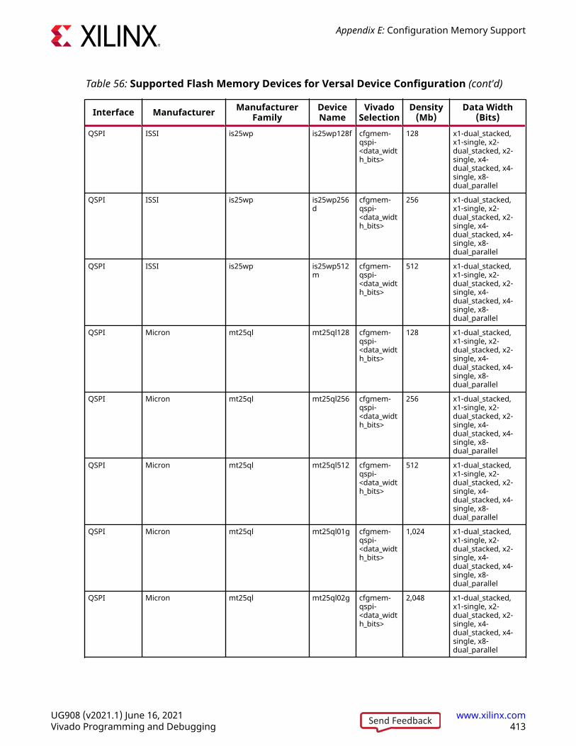
Table 56: Supported Flash Memory Devices for Versal Device Configuration (cont'd)
Interface Manufacturer ManufacturerFamily
DeviceName
VivadoSelection
Density(Mb)
Data Width(Bits)
QSPI ISSI is25wp is25wp128f cfgmem-qspi-<data_width_bits>
128 x1-dual_stacked,x1-single, x2-dual_stacked, x2-single, x4-dual_stacked, x4-single, x8-dual_parallel
QSPI ISSI is25wp is25wp256d
cfgmem-qspi-<data_width_bits>
256 x1-dual_stacked,x1-single, x2-dual_stacked, x2-single, x4-dual_stacked, x4-single, x8-dual_parallel
QSPI ISSI is25wp is25wp512m
cfgmem-qspi-<data_width_bits>
512 x1-dual_stacked,x1-single, x2-dual_stacked, x2-single, x4-dual_stacked, x4-single, x8-dual_parallel
QSPI Micron mt25ql mt25ql128 cfgmem-qspi-<data_width_bits>
128 x1-dual_stacked,x1-single, x2-dual_stacked, x2-single, x4-dual_stacked, x4-single, x8-dual_parallel
QSPI Micron mt25ql mt25ql256 cfgmem-qspi-<data_width_bits>
256 x1-dual_stacked,x1-single, x2-dual_stacked, x2-single, x4-dual_stacked, x4-single, x8-dual_parallel
QSPI Micron mt25ql mt25ql512 cfgmem-qspi-<data_width_bits>
512 x1-dual_stacked,x1-single, x2-dual_stacked, x2-single, x4-dual_stacked, x4-single, x8-dual_parallel
QSPI Micron mt25ql mt25ql01g cfgmem-qspi-<data_width_bits>
1,024 x1-dual_stacked,x1-single, x2-dual_stacked, x2-single, x4-dual_stacked, x4-single, x8-dual_parallel
QSPI Micron mt25ql mt25ql02g cfgmem-qspi-<data_width_bits>
2,048 x1-dual_stacked,x1-single, x2-dual_stacked, x2-single, x4-dual_stacked, x4-single, x8-dual_parallel
Appendix E: Configuration Memory Support
UG908 (v2021.1) June 16, 2021 www.xilinx.comVivado Programming and Debugging 413Send Feedback
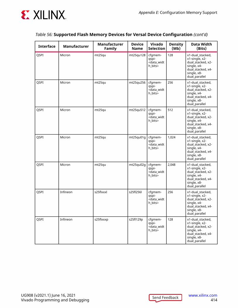
Table 56: Supported Flash Memory Devices for Versal Device Configuration (cont'd)
Interface Manufacturer ManufacturerFamily
DeviceName
VivadoSelection
Density(Mb)
Data Width(Bits)
QSPI Micron mt25qu mt25qu128 cfgmem-qspi-<data_width_bits>
128 x1-dual_stacked,x1-single, x2-dual_stacked, x2-single, x4-dual_stacked, x4-single, x8-dual_parallel
QSPI Micron mt25qu mt25qu256 cfgmem-qspi-<data_width_bits>
256 x1-dual_stacked,x1-single, x2-dual_stacked, x2-single, x4-dual_stacked, x4-single, x8-dual_parallel
QSPI Micron mt25qu mt25qu512 cfgmem-qspi-<data_width_bits>
512 x1-dual_stacked,x1-single, x2-dual_stacked, x2-single, x4-dual_stacked, x4-single, x8-dual_parallel
QSPI Micron mt25qu mt25qu01g cfgmem-qspi-<data_width_bits>
1,024 x1-dual_stacked,x1-single, x2-dual_stacked, x2-single, x4-dual_stacked, x4-single, x8-dual_parallel
QSPI Micron mt25qu mt25qu02g cfgmem-qspi-<data_width_bits>
2,048 x1-dual_stacked,x1-single, x2-dual_stacked, x2-single, x4-dual_stacked, x4-single, x8-dual_parallel
QSPI Infineon s25flxxxl s25fl256l cfgmem-qspi-<data_width_bits>
256 x1-dual_stacked,x1-single, x2-dual_stacked, x2-single, x4-dual_stacked, x4-single, x8-dual_parallel
QSPI Infineon s25flxxxp s25fl129p cfgmem-qspi-<data_width_bits>
128 x1-dual_stacked,x1-single, x2-dual_stacked, x2-single, x4-dual_stacked, x4-single, x8-dual_parallel
Appendix E: Configuration Memory Support
UG908 (v2021.1) June 16, 2021 www.xilinx.comVivado Programming and Debugging 414Send Feedback
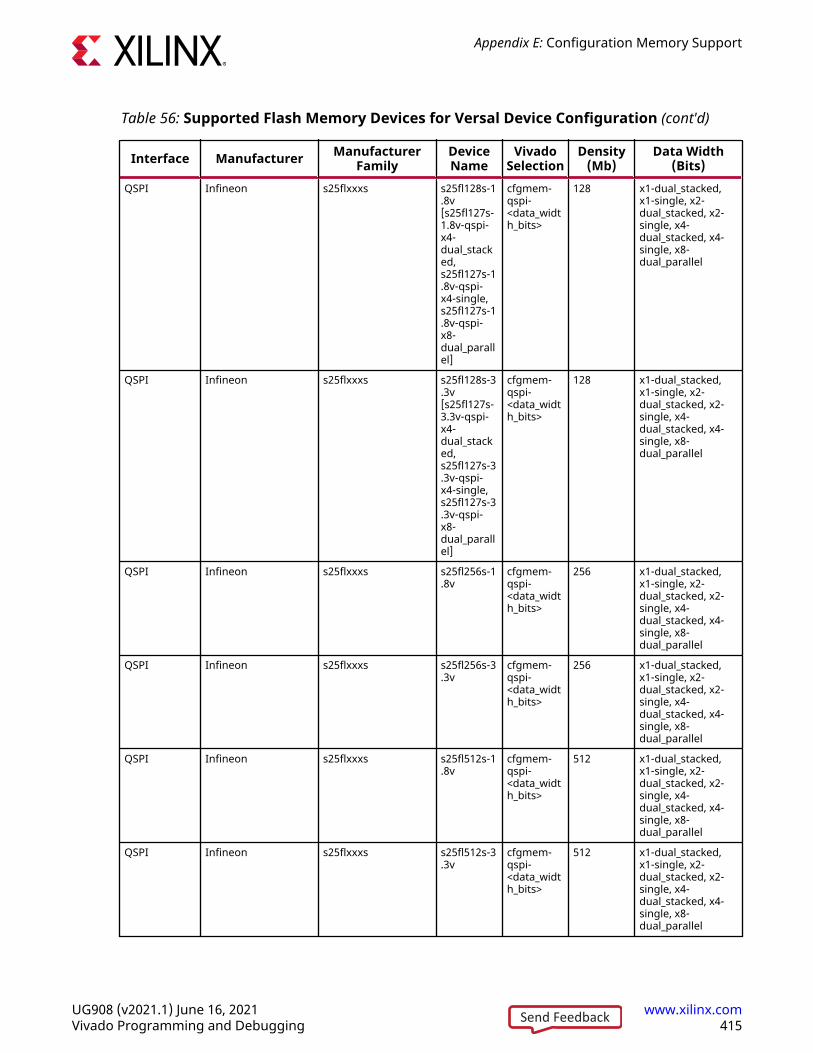
Table 56: Supported Flash Memory Devices for Versal Device Configuration (cont'd)
Interface Manufacturer ManufacturerFamily
DeviceName
VivadoSelection
Density(Mb)
Data Width(Bits)
QSPI Infineon s25flxxxs s25fl128s-1.8v[s25fl127s-1.8v-qspi-x4-dual_stacked,s25fl127s-1.8v-qspi-x4-single,s25fl127s-1.8v-qspi-x8-dual_parallel]
cfgmem-qspi-<data_width_bits>
128 x1-dual_stacked,x1-single, x2-dual_stacked, x2-single, x4-dual_stacked, x4-single, x8-dual_parallel
QSPI Infineon s25flxxxs s25fl128s-3.3v[s25fl127s-3.3v-qspi-x4-dual_stacked,s25fl127s-3.3v-qspi-x4-single,s25fl127s-3.3v-qspi-x8-dual_parallel]
cfgmem-qspi-<data_width_bits>
128 x1-dual_stacked,x1-single, x2-dual_stacked, x2-single, x4-dual_stacked, x4-single, x8-dual_parallel
QSPI Infineon s25flxxxs s25fl256s-1.8v
cfgmem-qspi-<data_width_bits>
256 x1-dual_stacked,x1-single, x2-dual_stacked, x2-single, x4-dual_stacked, x4-single, x8-dual_parallel
QSPI Infineon s25flxxxs s25fl256s-3.3v
cfgmem-qspi-<data_width_bits>
256 x1-dual_stacked,x1-single, x2-dual_stacked, x2-single, x4-dual_stacked, x4-single, x8-dual_parallel
QSPI Infineon s25flxxxs s25fl512s-1.8v
cfgmem-qspi-<data_width_bits>
512 x1-dual_stacked,x1-single, x2-dual_stacked, x2-single, x4-dual_stacked, x4-single, x8-dual_parallel
QSPI Infineon s25flxxxs s25fl512s-3.3v
cfgmem-qspi-<data_width_bits>
512 x1-dual_stacked,x1-single, x2-dual_stacked, x2-single, x4-dual_stacked, x4-single, x8-dual_parallel
Appendix E: Configuration Memory Support
UG908 (v2021.1) June 16, 2021 www.xilinx.comVivado Programming and Debugging 415Send Feedback
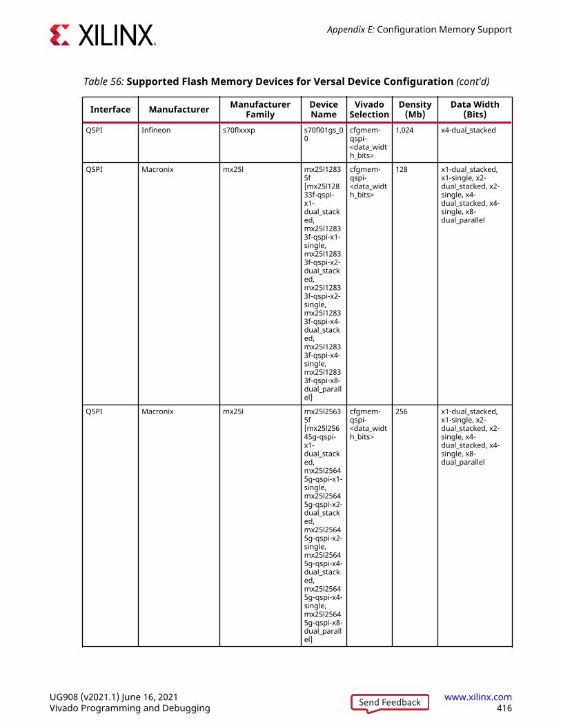
Table 56: Supported Flash Memory Devices for Versal Device Configuration (cont'd)
Interface Manufacturer ManufacturerFamily
DeviceName
VivadoSelection
Density(Mb)
Data Width(Bits)
QSPI Infineon s70flxxxp s70fl01gs_00
cfgmem-qspi-<data_width_bits>
1,024 x4-dual_stacked
QSPI Macronix mx25l mx25l12835f[mx25l12833f-qspi-x1-dual_stacked,mx25l12833f-qspi-x1-single,mx25l12833f-qspi-x2-dual_stacked,mx25l12833f-qspi-x2-single,mx25l12833f-qspi-x4-dual_stacked,mx25l12833f-qspi-x4-single,mx25l12833f-qspi-x8-dual_parallel]
cfgmem-qspi-<data_width_bits>
128 x1-dual_stacked,x1-single, x2-dual_stacked, x2-single, x4-dual_stacked, x4-single, x8-dual_parallel
QSPI Macronix mx25l mx25l25635f[mx25l25645g-qspi-x1-dual_stacked,mx25l25645g-qspi-x1-single,mx25l25645g-qspi-x2-dual_stacked,mx25l25645g-qspi-x2-single,mx25l25645g-qspi-x4-dual_stacked,mx25l25645g-qspi-x4-single,mx25l25645g-qspi-x8-dual_parallel]
cfgmem-qspi-<data_width_bits>
256 x1-dual_stacked,x1-single, x2-dual_stacked, x2-single, x4-dual_stacked, x4-single, x8-dual_parallel
Appendix E: Configuration Memory Support
UG908 (v2021.1) June 16, 2021 www.xilinx.comVivado Programming and Debugging 416Send Feedback
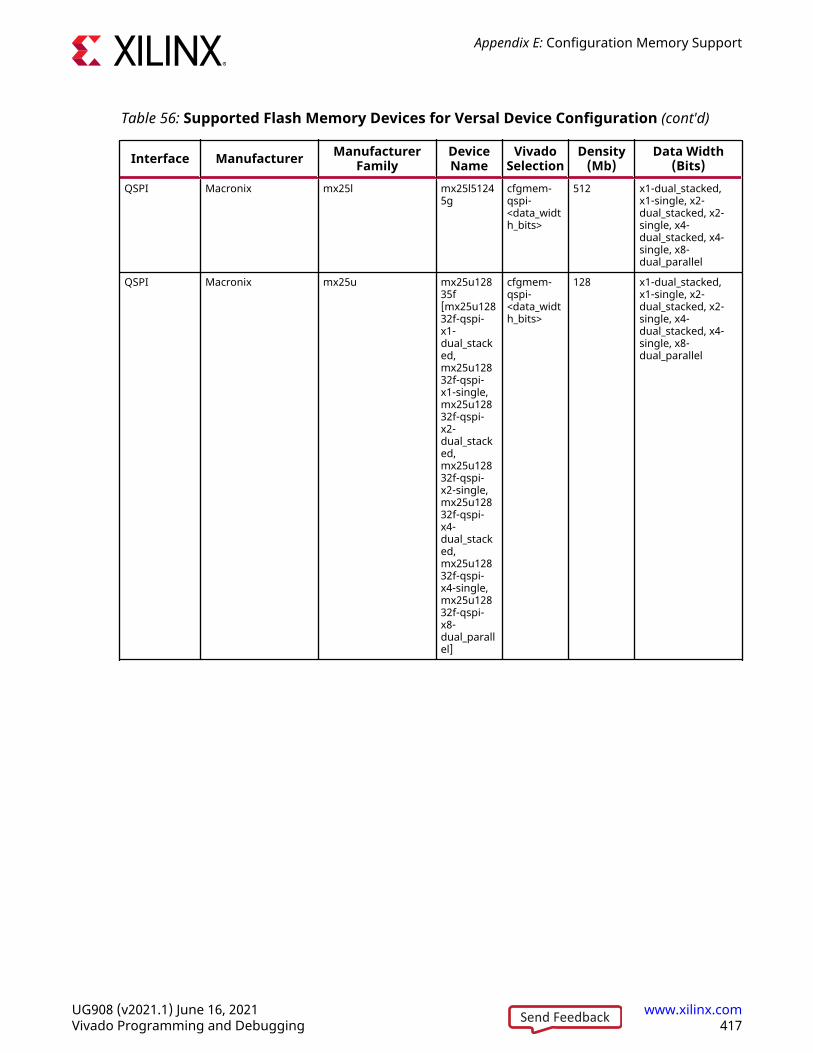
Table 56: Supported Flash Memory Devices for Versal Device Configuration (cont'd)
Interface Manufacturer ManufacturerFamily
DeviceName
VivadoSelection
Density(Mb)
Data Width(Bits)
QSPI Macronix mx25l mx25l51245g
cfgmem-qspi-<data_width_bits>
512 x1-dual_stacked,x1-single, x2-dual_stacked, x2-single, x4-dual_stacked, x4-single, x8-dual_parallel
QSPI Macronix mx25u mx25u12835f[mx25u12832f-qspi-x1-dual_stacked,mx25u12832f-qspi-x1-single,mx25u12832f-qspi-x2-dual_stacked,mx25u12832f-qspi-x2-single,mx25u12832f-qspi-x4-dual_stacked,mx25u12832f-qspi-x4-single,mx25u12832f-qspi-x8-dual_parallel]
cfgmem-qspi-<data_width_bits>
128 x1-dual_stacked,x1-single, x2-dual_stacked, x2-single, x4-dual_stacked, x4-single, x8-dual_parallel
Appendix E: Configuration Memory Support
UG908 (v2021.1) June 16, 2021 www.xilinx.comVivado Programming and Debugging 417Send Feedback
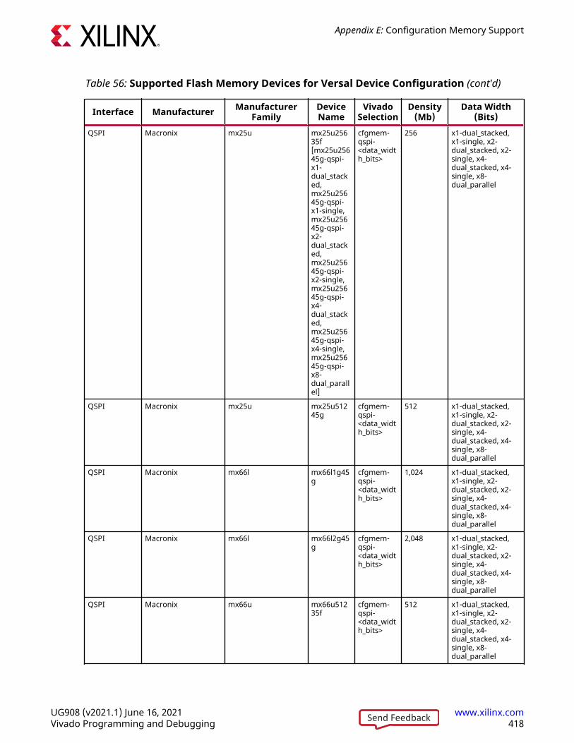
Table 56: Supported Flash Memory Devices for Versal Device Configuration (cont'd)
Interface Manufacturer ManufacturerFamily
DeviceName
VivadoSelection
Density(Mb)
Data Width(Bits)
QSPI Macronix mx25u mx25u25635f[mx25u25645g-qspi-x1-dual_stacked,mx25u25645g-qspi-x1-single,mx25u25645g-qspi-x2-dual_stacked,mx25u25645g-qspi-x2-single,mx25u25645g-qspi-x4-dual_stacked,mx25u25645g-qspi-x4-single,mx25u25645g-qspi-x8-dual_parallel]
cfgmem-qspi-<data_width_bits>
256 x1-dual_stacked,x1-single, x2-dual_stacked, x2-single, x4-dual_stacked, x4-single, x8-dual_parallel
QSPI Macronix mx25u mx25u51245g
cfgmem-qspi-<data_width_bits>
512 x1-dual_stacked,x1-single, x2-dual_stacked, x2-single, x4-dual_stacked, x4-single, x8-dual_parallel
QSPI Macronix mx66l mx66l1g45g
cfgmem-qspi-<data_width_bits>
1,024 x1-dual_stacked,x1-single, x2-dual_stacked, x2-single, x4-dual_stacked, x4-single, x8-dual_parallel
QSPI Macronix mx66l mx66l2g45g
cfgmem-qspi-<data_width_bits>
2,048 x1-dual_stacked,x1-single, x2-dual_stacked, x2-single, x4-dual_stacked, x4-single, x8-dual_parallel
QSPI Macronix mx66u mx66u51235f
cfgmem-qspi-<data_width_bits>
512 x1-dual_stacked,x1-single, x2-dual_stacked, x2-single, x4-dual_stacked, x4-single, x8-dual_parallel
Appendix E: Configuration Memory Support
UG908 (v2021.1) June 16, 2021 www.xilinx.comVivado Programming and Debugging 418Send Feedback
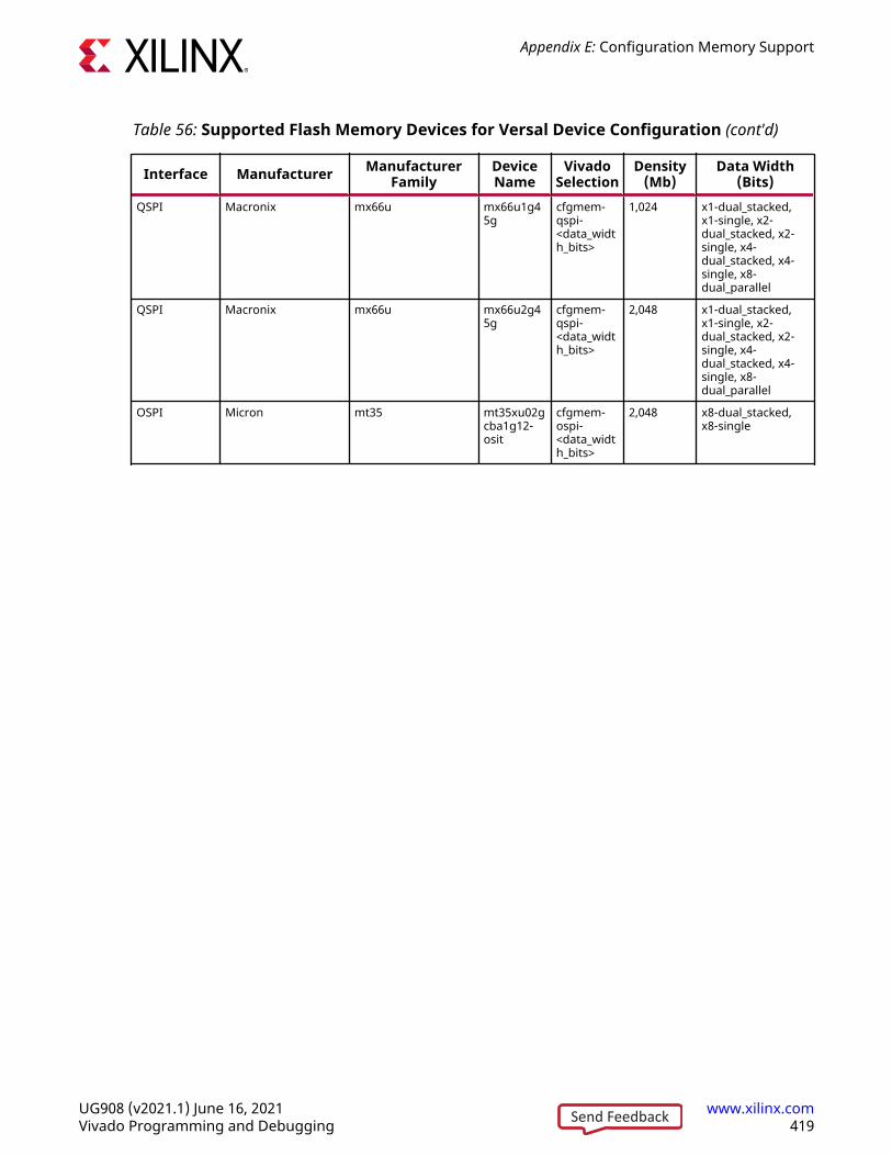
Table 56: Supported Flash Memory Devices for Versal Device Configuration (cont'd)
Interface Manufacturer ManufacturerFamily
DeviceName
VivadoSelection
Density(Mb)
Data Width(Bits)
QSPI Macronix mx66u mx66u1g45g
cfgmem-qspi-<data_width_bits>
1,024 x1-dual_stacked,x1-single, x2-dual_stacked, x2-single, x4-dual_stacked, x4-single, x8-dual_parallel
QSPI Macronix mx66u mx66u2g45g
cfgmem-qspi-<data_width_bits>
2,048 x1-dual_stacked,x1-single, x2-dual_stacked, x2-single, x4-dual_stacked, x4-single, x8-dual_parallel
OSPI Micron mt35 mt35xu02gcba1g12-osit
cfgmem-ospi-<data_width_bits>
2,048 x8-dual_stacked,x8-single
Appendix E: Configuration Memory Support
UG908 (v2021.1) June 16, 2021 www.xilinx.comVivado Programming and Debugging 419Send Feedback
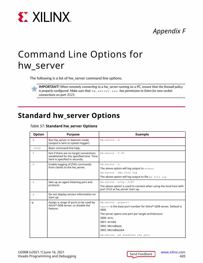
Appendix F
Command Line Options forhw_server
The following is a list of hw_server command line options.
IMPORTANT! When remotely connecting to a hw_server running on a PC, ensure that the firewall policyis properly configured. Make sure that hw_server.exe has permission to listen for new socketconnections on port 3121.
Standard hw_server OptionsTable 57: Standard hw_server Options
Option Purpose Example-d Run hw_server in daemon mode
(output is sent to system logger).hw_server -d
--help Basic command line help.-I Exit if there are no target connections
established for the specified time. Timehere is specified in seconds.
hw_server -I 20
-L Enable logging of JTAG commandsfrom clients to the hw_server.
hw_server -L-
The above option will log output to stdouthw_server -Lmy_file.log
The above option will log output to file my_file.log
-s Sets up an agent listening port andprotocol.
hw_server -stcp::3122
The above option is used to connect when using the local host withport 3122 at hw_server start up.
-q Do not display version information onstart up.
-p Assign a range of ports to be used byXilinx® GDB server, or disable thefeature.
hw_server -p<port>
<port> is the base port number for Xilinx® GDB server. Default is3000The server opens one port per target architecture:3000: Arm;3001: Arm64;3002: MicroBlaze;3003: MicroBlaze64hw_server -p0 disables the port
Appendix F: Command Line Options for hw_server
UG908 (v2021.1) June 16, 2021 www.xilinx.comVivado Programming and Debugging 420Send Feedback
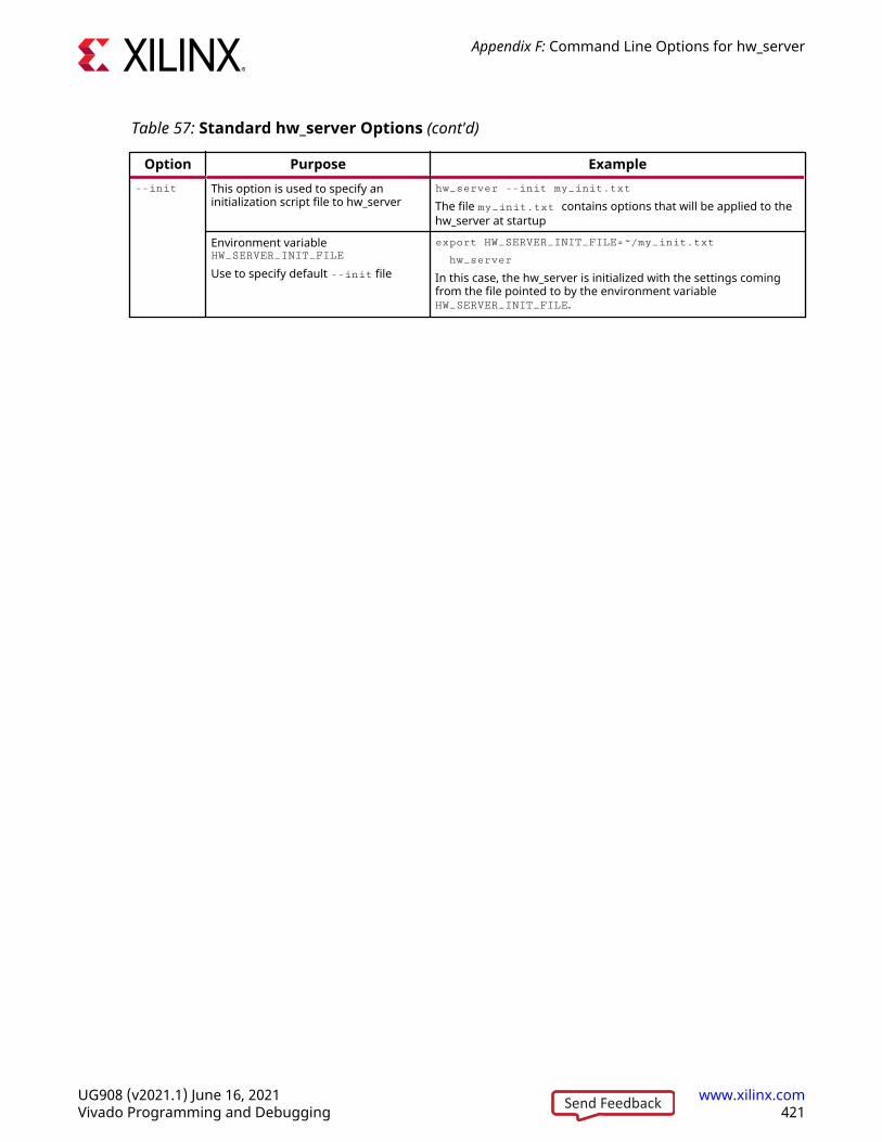
Table 57: Standard hw_server Options (cont'd)
Option Purpose Example--init This option is used to specify an
initialization script file to hw_serverhw_server --init my_init.txt
The file my_init.txt contains options that will be applied to thehw_server at startup
Environment variableHW_SERVER_INIT_FILE
Use to specify default --init file
export HW_SERVER_INIT_FILE=~/my_init.txt
hw_server
In this case, the hw_server is initialized with the settings comingfrom the file pointed to by the environment variableHW_SERVER_INIT_FILE.
Appendix F: Command Line Options for hw_server
UG908 (v2021.1) June 16, 2021 www.xilinx.comVivado Programming and Debugging 421Send Feedback
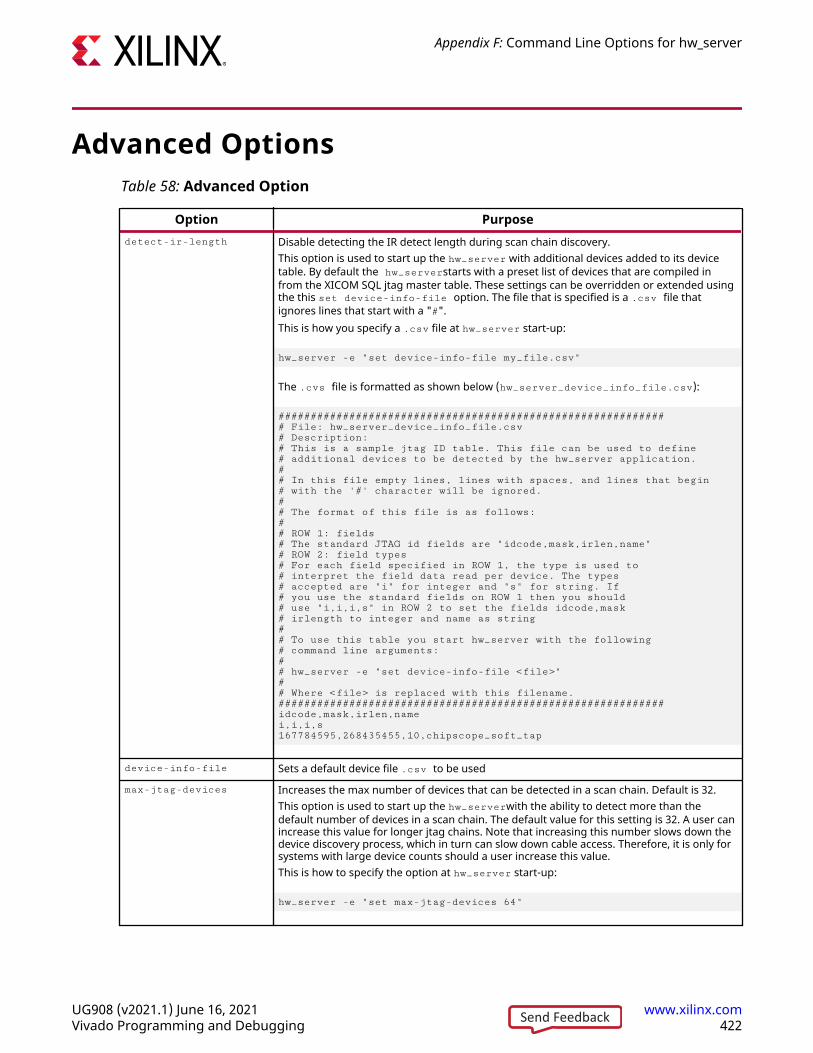
Advanced OptionsTable 58: Advanced Option
Option Purposedetect-ir-length Disable detecting the IR detect length during scan chain discovery.
This option is used to start up the hw_server with additional devices added to its devicetable. By default the hw_serverstarts with a preset list of devices that are compiled infrom the XICOM SQL jtag master table. These settings can be overridden or extended usingthe this set device-info-file option. The file that is specified is a .csv file thatignores lines that start with a "#".This is how you specify a .csv file at hw_server start-up:
hw_server -e "set device-info-file my_file.csv"
The .cvs file is formatted as shown below (hw_server_device_info_file.csv):
############################################################# File: hw_server_device_info_file.csv# Description:# This is a sample jtag ID table. This file can be used to define# additional devices to be detected by the hw_server application.## In this file empty lines, lines with spaces, and lines that begin# with the '#' character will be ignored.## The format of this file is as follows:## ROW 1: fields# The standard JTAG id fields are "idcode,mask,irlen,name"# ROW 2: field types# For each field specified in ROW 1, the type is used to# interpret the field data read per device. The types# accepted are "i" for integer and "s" for string. If# you use the standard fields on ROW 1 then you should# use "i,i,i,s" in ROW 2 to set the fields idcode,mask# irlength to integer and name as string## To use this table you start hw_server with the following# command line arguments:## hw_server -e "set device-info-file <file>"## Where <file> is replaced with this filename.############################################################idcode,mask,irlen,namei,i,i,s167784595,268435455,10,chipscope_soft_tap
device-info-file Sets a default device file .csv to be used
max-jtag-devices Increases the max number of devices that can be detected in a scan chain. Default is 32.This option is used to start up the hw_serverwith the ability to detect more than thedefault number of devices in a scan chain. The default value for this setting is 32. A user canincrease this value for longer jtag chains. Note that increasing this number slows down thedevice discovery process, which in turn can slow down cable access. Therefore, it is only forsystems with large device counts should a user increase this value.This is how to specify the option at hw_server start-up:
hw_server -e "set max-jtag-devices 64"
Appendix F: Command Line Options for hw_server
UG908 (v2021.1) June 16, 2021 www.xilinx.comVivado Programming and Debugging 422Send Feedback
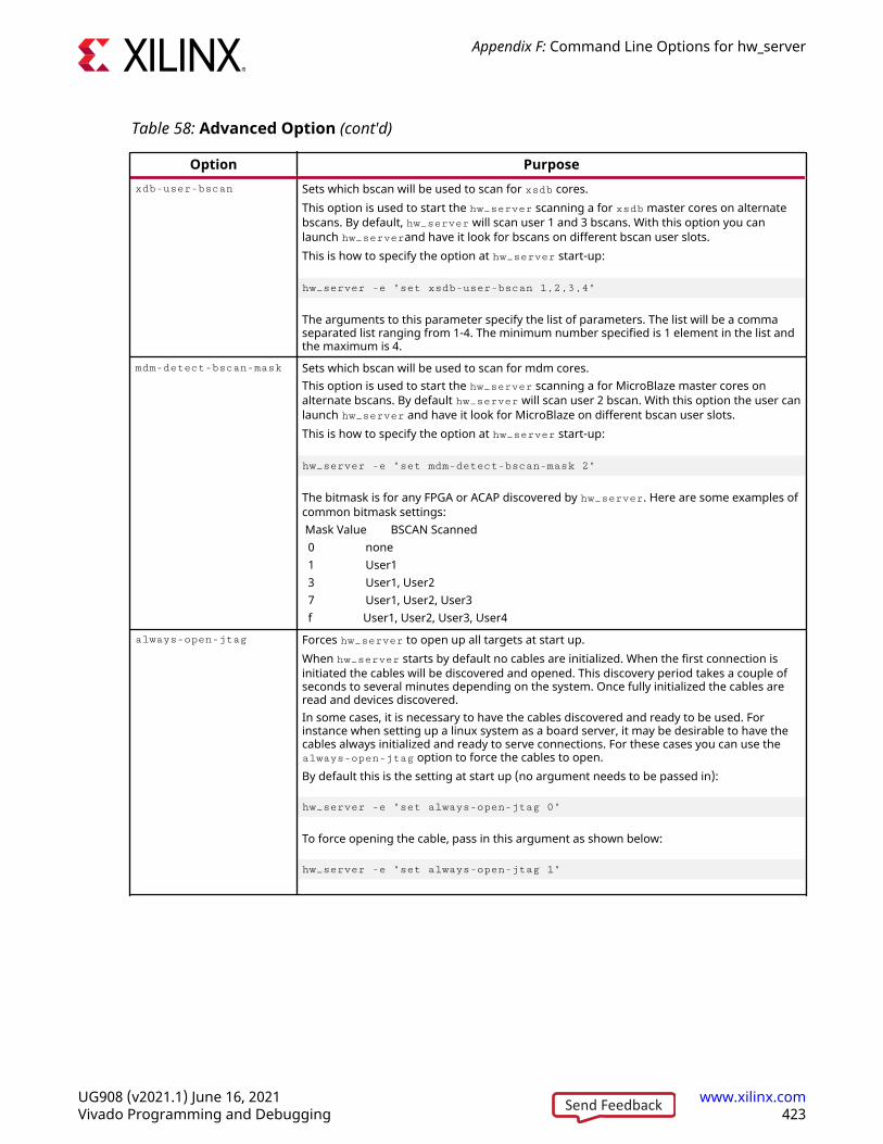
Table 58: Advanced Option (cont'd)
Option Purposexdb-user-bscan Sets which bscan will be used to scan for xsdb cores.
This option is used to start the hw_server scanning a for xsdb master cores on alternatebscans. By default, hw_server will scan user 1 and 3 bscans. With this option you canlaunch hw_serverand have it look for bscans on different bscan user slots.This is how to specify the option at hw_server start-up:
hw_server -e "set xsdb-user-bscan 1,2,3,4"
The arguments to this parameter specify the list of parameters. The list will be a commaseparated list ranging from 1-4. The minimum number specified is 1 element in the list andthe maximum is 4.
mdm-detect-bscan-mask Sets which bscan will be used to scan for mdm cores.This option is used to start the hw_server scanning a for MicroBlaze master cores onalternate bscans. By default hw_server will scan user 2 bscan. With this option the user canlaunch hw_server and have it look for MicroBlaze on different bscan user slots.This is how to specify the option at hw_server start-up:
hw_server -e "set mdm-detect-bscan-mask 2"
The bitmask is for any FPGA or ACAP discovered by hw_server. Here are some examples ofcommon bitmask settings: Mask Value BSCAN Scanned 0 none 1 User1 3 User1, User2 7 User1, User2, User3 f User1, User2, User3, User4
always-open-jtag Forces hw_server to open up all targets at start up.When hw_server starts by default no cables are initialized. When the first connection isinitiated the cables will be discovered and opened. This discovery period takes a couple ofseconds to several minutes depending on the system. Once fully initialized the cables areread and devices discovered.In some cases, it is necessary to have the cables discovered and ready to be used. Forinstance when setting up a linux system as a board server, it may be desirable to have thecables always initialized and ready to serve connections. For these cases you can use thealways-open-jtag option to force the cables to open.By default this is the setting at start up (no argument needs to be passed in):
hw_server -e "set always-open-jtag 0"
To force opening the cable, pass in this argument as shown below:
hw_server -e "set always-open-jtag 1"
Appendix F: Command Line Options for hw_server
UG908 (v2021.1) June 16, 2021 www.xilinx.comVivado Programming and Debugging 423Send Feedback
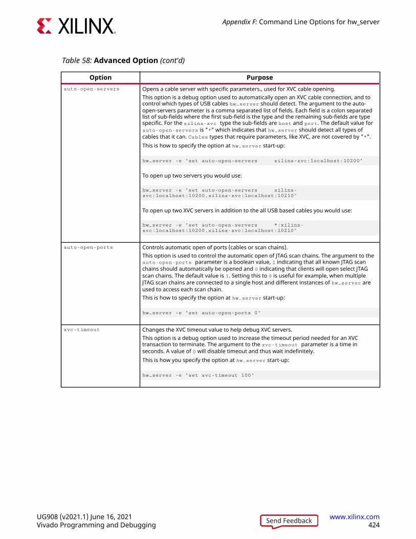
Table 58: Advanced Option (cont'd)
Option Purposeauto-open-servers Opens a cable server with specific parameters., used for XVC cable opening.
This option is a debug option used to automatically open an XVC cable connection, and tocontrol which types of USB cables hw_server should detect. The argument to the auto-open-servers parameter is a comma separated list of fields. Each field is a colon separatedlist of sub-fields where the first sub-field is the type and the remaining sub-fields are typespecific. For the xilinx-xvc type the sub-fields are host and port. The default value forauto-open-servers is "*" which indicates that hw_server should detect all types ofcables that it can. Cables types that require parameters, like XVC, are not covered by "*".This is how to specify the option at hw_server start-up:
hw_server -e "set auto-open-servers xilinx-xvc:localhost:10200"
To open up two servers you would use:
hw_server -e "set auto-open-servers xilinx-xvc:localhost:10200,xilinx-xvc:localhost:10210"
To open up two XVC servers in addition to the all USB based cables you would use:
hw_server -e "set auto-open-servers *:xilinx-xvc:localhost:10200,xilinx-xvc:localhost:10210"
auto-open-ports Controls automatic open of ports (cables or scan chains).This option is used to control the automatic open of JTAG scan chains. The argument to theauto-open-ports parameter is a boolean value, 1 indicating that all known JTAG scanchains should automatically be opened and 0 indicating that clients will open select JTAGscan chains. The default value is 1. Setting this to 0 is useful for example, when multipleJTAG scan chains are connected to a single host and different instances of hw_server areused to access each scan chain.This is how to specify the option at hw_server start-up:
hw_server -e "set auto-open-ports 0"
xvc-timeout Changes the XVC timeout value to help debug XVC servers.This option is a debug option used to increase the timeout period needed for an XVCtransaction to terminate. The argument to the xvc-timeout parameter is a time inseconds. A value of 0 will disable timeout and thus wait indefinitely.This is how you specify the option at hw_server start-up:
hw_server -e "set xvc-timeout 100"
Appendix F: Command Line Options for hw_server
UG908 (v2021.1) June 16, 2021 www.xilinx.comVivado Programming and Debugging 424Send Feedback
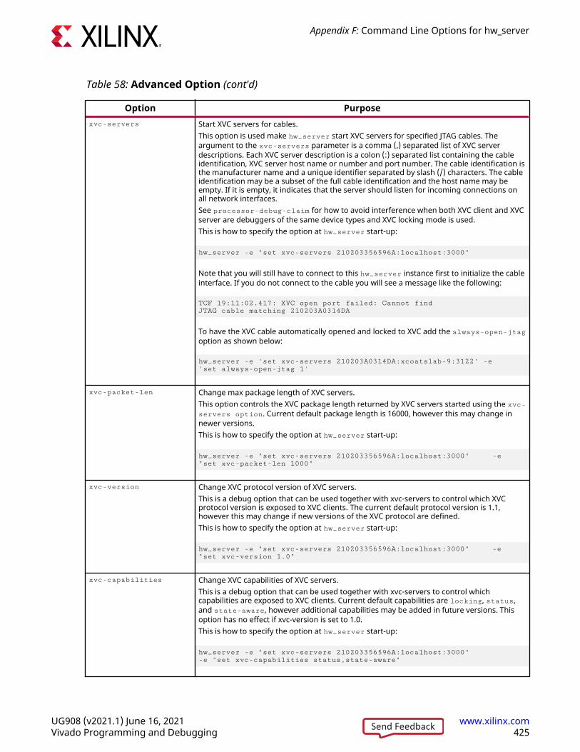
Table 58: Advanced Option (cont'd)
Option Purposexvc-servers Start XVC servers for cables.
This option is used make hw_server start XVC servers for specified JTAG cables. Theargument to the xvc-servers parameter is a comma (,) separated list of XVC serverdescriptions. Each XVC server description is a colon (:) separated list containing the cableidentification, XVC server host name or number and port number. The cable identification isthe manufacturer name and a unique identifier separated by slash (/) characters. The cableidentification may be a subset of the full cable identification and the host name may beempty. If it is empty, it indicates that the server should listen for incoming connections onall network interfaces.See processor-debug-claim for how to avoid interference when both XVC client and XVCserver are debuggers of the same device types and XVC locking mode is used.This is how to specify the option at hw_server start-up:
hw_server -e "set xvc-servers 210203356596A:localhost:3000"
Note that you will still have to connect to this hw_server instance first to initialize the cableinterface. If you do not connect to the cable you will see a message like the following:
TCF 19:11:02.417: XVC open port failed: Cannot findJTAG cable matching 210203A0314DA
To have the XVC cable automatically opened and locked to XVC add the always-open-jtagoption as shown below:
hw_server -e 'set xvc-servers 210203A0314DA:xcoatslab-9:3122' -e'set always-open-jtag 1'
xvc-packet-len Change max package length of XVC servers.This option controls the XVC package length returned by XVC servers started using the xvc-servers option. Current default package length is 16000, however this may change innewer versions.This is how to specify the option at hw_server start-up:
hw_server -e "set xvc-servers 210203356596A:localhost:3000" -e "set xvc-packet-len 1000"
xvc-version Change XVC protocol version of XVC servers.This is a debug option that can be used together with xvc-servers to control which XVCprotocol version is exposed to XVC clients. The current default protocol version is 1.1,however this may change if new versions of the XVC protocol are defined.This is how to specify the option at hw_server start-up:
hw_server -e "set xvc-servers 210203356596A:localhost:3000" -e "set xvc-version 1.0"
xvc-capabilities Change XVC capabilities of XVC servers.This is a debug option that can be used together with xvc-servers to control whichcapabilities are exposed to XVC clients. Current default capabilities are locking, status,and state-aware, however additional capabilities may be added in future versions. Thisoption has no effect if xvc-version is set to 1.0.This is how to specify the option at hw_server start-up:
hw_server -e "set xvc-servers 210203356596A:localhost:3000"-e "set xvc-capabilities status,state-aware"
Appendix F: Command Line Options for hw_server
UG908 (v2021.1) June 16, 2021 www.xilinx.comVivado Programming and Debugging 425Send Feedback
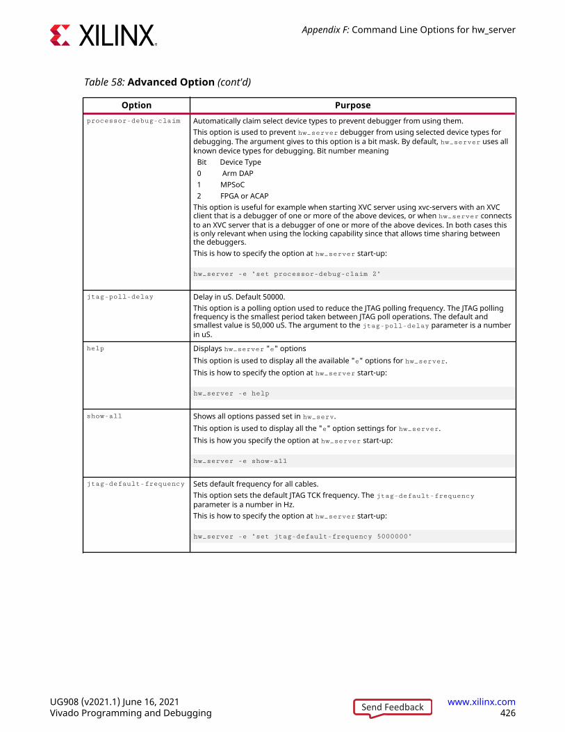
Table 58: Advanced Option (cont'd)
Option Purposeprocessor-debug-claim Automatically claim select device types to prevent debugger from using them.
This option is used to prevent hw_server debugger from using selected device types fordebugging. The argument gives to this option is a bit mask. By default, hw_server uses allknown device types for debugging. Bit number meaning Bit Device Type 0 Arm DAP 1 MPSoC 2 FPGA or ACAPThis option is useful for example when starting XVC server using xvc-servers with an XVCclient that is a debugger of one or more of the above devices, or when hw_server connectsto an XVC server that is a debugger of one or more of the above devices. In both cases thisis only relevant when using the locking capability since that allows time sharing betweenthe debuggers.This is how to specify the option at hw_server start-up:
hw_server -e "set processor-debug-claim 2"
jtag-poll-delay Delay in uS. Default 50000.This option is a polling option used to reduce the JTAG polling frequency. The JTAG pollingfrequency is the smallest period taken between JTAG poll operations. The default andsmallest value is 50,000 uS. The argument to the jtag-poll-delay parameter is a numberin uS.
help Displays hw_server "e" optionsThis option is used to display all the available "e" options for hw_server.This is how to specify the option at hw_server start-up:
hw_server -e help
show-all Shows all options passed set in hw_serv.This option is used to display all the "e" option settings for hw_server.This is how you specify the option at hw_server start-up:
hw_server -e show-all
jtag-default-frequency Sets default frequency for all cables.This option sets the default JTAG TCK frequency. The jtag-default-frequencyparameter is a number in Hz.This is how to specify the option at hw_server start-up:
hw_server -e "set jtag-default-frequency 5000000"
Appendix F: Command Line Options for hw_server
UG908 (v2021.1) June 16, 2021 www.xilinx.comVivado Programming and Debugging 426Send Feedback
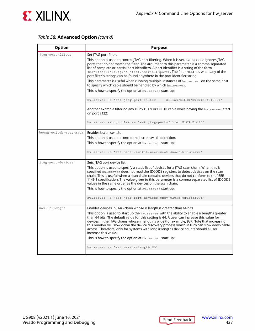
Table 58: Advanced Option (cont'd)
Option Purposejtag-port-filter Set JTAG port filter.
This option is used to control JTAG port filtering. When it is set, hw_server ignores JTAGports that do not match the filter. The argument to this parameter is a comma separatedlist of complete or partial port identifiers. A port identifier is a string of the form<manufacturer>/<productid>/<serial><port>. The filter matches when any of theport filter's strings can be found anywhere in the port identifier string.This parameter is useful when running multiple instances of hw_server on the same hostto specify which cable should be handled by which hw_server.This is how to specify the option at hw_server start-up:
hw_server -e "set jtag-port-filter Xilinx/DLC10/0000128f515601"
Another example filtering any Xilinx DLC9 or DLC10 cable while having the hw_server starton port 3122:
hw_server -stcp::3122 -e "set jtag-port-filter DLC9,DLC10"
bscan-switch-user-mask Enables bscan switch.This option is used to control the bscan switch detection.This is how to specify the option at hw_server start-up:
hw_server -e "set bscan-switch-user-mask <user-bit-mask>"
jtag-port-devices Sets JTAG port device list.This option is used to specify a static list of devices for a JTAG scan chain. When this isspecified hw_server does not read the IDCODE registers to detect devices on the scanchain. This is useful when a scan chain contains devices that do not conform to the IEEE1149.1 specification. The value given to this parameter is a comma separated list of IDCODEvalues in the same order as the devices on the scan chain.This is how to specify the option at hw_server start-up:
hw_server -e "set jtag-port-devices 0xe970203f,0x03632093"
max-ir-length Enables devices in JTAG chain whose ir length is greater than 64 bits.This option is used to start up the hw_server with the ability to enable ir lengths greaterthan 64 bits. The default value for this setting is 64. A user can increase this value fordevices in the JTAG chains whose ir length is wide (for example, 93). Note that increasingthis number will slow down the device discovery process which in turn can slow down cableaccess. Therefore, only for systems with long ir lengths device counts should a userincrease this value.This is how to specify the option at hw_server start-up:
hw_server -e "set max-ir-length 93"
Appendix F: Command Line Options for hw_server
UG908 (v2021.1) June 16, 2021 www.xilinx.comVivado Programming and Debugging 427Send Feedback

Appendix G
Additional Resources and LegalNotices
Xilinx ResourcesFor support resources such as Answers, Documentation, Downloads, and Forums, see XilinxSupport.
Solution CentersSee the Xilinx Solution Centers for support on devices, software tools, and intellectual propertyat all stages of the design cycle. Topics include design assistance, advisories, and troubleshootingtips.
Documentation Navigator and Design HubsXilinx® Documentation Navigator (DocNav) provides access to Xilinx documents, videos, andsupport resources, which you can filter and search to find information. To open DocNav:
• From the Vivado® IDE, select Help → Documentation and Tutorials.
• On Windows, select Start → All Programs → Xilinx Design Tools → DocNav.
• At the Linux command prompt, enter docnav.
Xilinx Design Hubs provide links to documentation organized by design tasks and other topics,which you can use to learn key concepts and address frequently asked questions. To access theDesign Hubs:
• In DocNav, click the Design Hubs View tab.
• On the Xilinx website, see the Design Hubs page.
Appendix G: Additional Resources and Legal Notices
UG908 (v2021.1) June 16, 2021 www.xilinx.comVivado Programming and Debugging 428Send Feedback
Note: For more information on DocNav, see the Documentation Navigator page on the Xilinx website.
ReferencesThese documents provide supplemental material useful with this guide:
1. Vivado Design Suite Documentation
2. Vivado Design Suite User Guide: Logic Simulation (UG900)
3. Vivado Design Suite User Guide: Synthesis (UG901)
4. Vivado Design Suite User Guide: Dynamic Function eXchange (UG909)
5. Vivado Design Suite Tutorial: Dynamic Function eXchange (UG947)
6. UltraFast Design Methodology Guide for Xilinx FPGAs and SoCs (UG949)
7. Vivado Design Suite User Guide: Implementation (UG904)
8. Vivado Design Suite User Guide: Release Notes, Installation, and Licensing (UG973)
9. Vivado Design Suite User Guide: Design Flows Overview (UG892)
10. Vivado Design Suite User Guide: I/O and Clock Planning (UG899)
11. Vivado Design Suite Tutorial: Programming and Debugging (UG936)
12. Vivado Design Suite Tcl Command Reference Guide (UG835)
13. SmartLynq Data Cable User Guide (UG1258)
14. 7 Series FPGAs Configuration User Guide (UG470)
15. 7 Series FPGAs and Zynq-7000 SoC XADC Dual 12-Bit 1 MSPS Analog-to-Digital Converter UserGuide (UG480)
16. UltraScale Architecture Configuration User Guide (UG570)
17. UltraScale Architecture System Monitor User Guide (UG580)
18. Vivado Design Suite User Guide: Designing IP Subsystems Using IP Integrator (UG994)
19. Virtex UltraScale+ FPGAs GTM Transceivers User Guide (UG581)
20. Debug Bridge LogiCORE IP Product Guide (PG245)
21. Xilinx Virtual Cable Running on Zynq-7000 Using the PetaLinux Tools (XAPP1251)
22. Vivado Design Suite Tutorial: Embedded Processor Hardware Design (UG940)
23. Xilinx In-System Programming Using an Embedded Microcontroller (ISE Tools) (XAPP058)
24. Using Encryption to Secure a 7 Series FPGA Bitstream (XAPP1239)
25. Using Encryption and Authentication to Secure an UltraScale/UltraScale+ FPGA Bitstream(XAPP1267)
Appendix G: Additional Resources and Legal Notices
UG908 (v2021.1) June 16, 2021 www.xilinx.comVivado Programming and Debugging 429Send Feedback

26. Virtual Input/Output LogiCORE IP Product Guide (PG159)
27. Integrated Bit Error Ratio Tester 7 Series GTX Transceivers LogiCORE IP Product Guide (PG132)
28. Integrated Bit Error Ratio Tester 7 Series GTP Transceivers LogiCORE IP Product Guide (PG133)
29. Integrated Bit Error Ratio Tester 7 Series GTH Transceivers LogiCORE IP Product Guide (PG152)
30. Integrated Logic Analyzer LogiCORE IP Product Guide (PG172)
31. JTAG to AXI Master LogiCORE IP Product Guide (PG174)
32. System Integrated Logic Analyzer LogiCORE IP Product Guide (PG261)
33. UltraScale+ Devices Integrated Block for PCI Express LogiCORE IP Product Guide (PG213)
34. Debug Bridge LogiCORE IP Product Guide (PG245)
35. In-System IBERT LogiCORE IP Product Guide (PG246)
36. UltraScale Architecture-Based FPGAs Memory IP LogiCORE IP Product Guide (PG150)
37. AXI High Bandwidth Controller LogiCORE IP Product Guide (PG276)
38. IBERT for UltraScale GTM Transceivers LogiCORE IP Product Guide (PG342)
39. Control, Interface and Processing System LogiCORE IP Product Guide (PG352)
Training CoursesXilinx provides a variety of training courses and QuickTake videos to help you learn more aboutthe concepts presented in this document. Use these links to explore related training:
1. Designing FPGAs Using the Vivado Design Suite 1
2. Designing FPGAs Using the Vivado Design Suite 2
3. Designing FPGAs Using the Vivado Design Suite 3
4. Designing FPGAs Using the Vivado Design Suite 4
5. Vivado Design Suite QuickTake Video: Targeting Zynq Devices Using Vivado IP Integrator
6. Vivado Design Suite QuickTake Video: Partial Reconfiguration in Vivado Design Suite
7. Vivado Design Suite QuickTake Video: Using Vivado Design Suite with Revision Control
8. Vivado Design Suite QuickTake Video Tutorials
Appendix G: Additional Resources and Legal Notices
UG908 (v2021.1) June 16, 2021 www.xilinx.comVivado Programming and Debugging 430Send Feedback

Please Read: Important Legal NoticesThe information disclosed to you hereunder (the "Materials") is provided solely for the selectionand use of Xilinx products. To the maximum extent permitted by applicable law: (1) Materials aremade available "AS IS" and with all faults, Xilinx hereby DISCLAIMS ALL WARRANTIES ANDCONDITIONS, EXPRESS, IMPLIED, OR STATUTORY, INCLUDING BUT NOT LIMITED TOWARRANTIES OF MERCHANTABILITY, NON-INFRINGEMENT, OR FITNESS FOR ANYPARTICULAR PURPOSE; and (2) Xilinx shall not be liable (whether in contract or tort, includingnegligence, or under any other theory of liability) for any loss or damage of any kind or naturerelated to, arising under, or in connection with, the Materials (including your use of theMaterials), including for any direct, indirect, special, incidental, or consequential loss or damage(including loss of data, profits, goodwill, or any type of loss or damage suffered as a result of anyaction brought by a third party) even if such damage or loss was reasonably foreseeable or Xilinxhad been advised of the possibility of the same. Xilinx assumes no obligation to correct anyerrors contained in the Materials or to notify you of updates to the Materials or to productspecifications. You may not reproduce, modify, distribute, or publicly display the Materialswithout prior written consent. Certain products are subject to the terms and conditions ofXilinx's limited warranty, please refer to Xilinx's Terms of Sale which can be viewed at https://www.xilinx.com/legal.htm#tos; IP cores may be subject to warranty and support terms containedin a license issued to you by Xilinx. Xilinx products are not designed or intended to be fail-safe orfor use in any application requiring fail-safe performance; you assume sole risk and liability foruse of Xilinx products in such critical applications, please refer to Xilinx's Terms of Sale which canbe viewed at https://www.xilinx.com/legal.htm#tos.
AUTOMOTIVE APPLICATIONS DISCLAIMER
AUTOMOTIVE PRODUCTS (IDENTIFIED AS "XA" IN THE PART NUMBER) ARE NOTWARRANTED FOR USE IN THE DEPLOYMENT OF AIRBAGS OR FOR USE IN APPLICATIONSTHAT AFFECT CONTROL OF A VEHICLE ("SAFETY APPLICATION") UNLESS THERE IS ASAFETY CONCEPT OR REDUNDANCY FEATURE CONSISTENT WITH THE ISO 26262AUTOMOTIVE SAFETY STANDARD ("SAFETY DESIGN"). CUSTOMER SHALL, PRIOR TO USINGOR DISTRIBUTING ANY SYSTEMS THAT INCORPORATE PRODUCTS, THOROUGHLY TESTSUCH SYSTEMS FOR SAFETY PURPOSES. USE OF PRODUCTS IN A SAFETY APPLICATIONWITHOUT A SAFETY DESIGN IS FULLY AT THE RISK OF CUSTOMER, SUBJECT ONLY TOAPPLICABLE LAWS AND REGULATIONS GOVERNING LIMITATIONS ON PRODUCTLIABILITY.
Appendix G: Additional Resources and Legal Notices
UG908 (v2021.1) June 16, 2021 www.xilinx.comVivado Programming and Debugging 431Send Feedback

Copyright
© Copyright 2012-2021 Xilinx, Inc. Xilinx, the Xilinx logo, Alveo, Artix, Kintex, Spartan, Versal,Virtex, Vivado, Zynq, and other designated brands included herein are trademarks of Xilinx in theUnited States and other countries. AMBA, AMBA Designer, Arm, ARM1176JZ-S, CoreSight,Cortex, PrimeCell, Mali, and MPCore are trademarks of Arm Limited in the EU and othercountries. PCI, PCIe, and PCI Express are trademarks of PCI-SIG and used under license. All othertrademarks are the property of their respective owners.
Appendix G: Additional Resources and Legal Notices
UG908 (v2021.1) June 16, 2021 www.xilinx.comVivado Programming and Debugging 432Send Feedback


![Vivado Design Suite User Guide: Implementation...Suite User Guide: Programming and Debugging (UG908) [Ref 12]. Note: The Vivado Design Suite supports Module Analysis, which is the](https://img.pdfslide.net/doc/110x75/60dbb37e5f868c057e2764c3/vivado-design-suite-user-guide-implementation-suite-user-guide-programming.jpg)