Embed Size (px)
Citation preview

Vivado Design Suite User Guide
Power Analysis and Optimization
UG907 (v2012.2) July 25, 2012

Power Analysis and Optimization www.xilinx.com 2UG907 (v2012.2) July 25, 2012
Notice of DisclaimerThe information disclosed to you hereunder (the “Materials”) is provided solely for the selection and use of Xilinx products. To the maximum extent permitted by applicable law: (1) Materials are made available "AS IS" and with all faults, Xilinx hereby DISCLAIMS ALL WARRANTIES AND CONDITIONS, EXPRESS, IMPLIED, OR STATUTORY, INCLUDING BUT NOT LIMITED TO WARRANTIES OF MERCHANTABILITY, NON-INFRINGEMENT, OR FITNESS FOR ANY PARTICULAR PURPOSE; and (2) Xilinx shall not be liable (whether in contract or tort, including negligence, or under any other theory of liability) for any loss or damage of any kind or nature related to, arising under, or in connection with, the Materials (including your use of the Materials), including for any direct, indirect, special, incidental, or consequential loss or damage (including loss of data, profits, goodwill, or any type of loss or damage suffered as a result of any action brought by a third party) even if such damage or loss was reasonably foreseeable or Xilinx had been advised of the possibility of the same. Xilinx assumes no obligation to correct any errors contained in the Materials or to notify you of updates to the Materials or to product specifications. You may not reproduce, modify, distribute, or publicly display the Materials without prior written consent. Certain products are subject to the terms and conditions of the Limited Warranties which can be viewed at http://www.xilinx.com/warranty.htm; IP cores may be subject to warranty and support terms contained in a license issued to you by Xilinx. Xilinx products are not designed or intended to be fail-safe or for use in any application requiring fail-safe performance; you assume sole risk and liability for use of Xilinx products in Critical Applications: http://www.xilinx.com/warranty.htm#critapps.© Copyright 2012 Xilinx, Inc. Xilinx, the Xilinx logo, Artix, ISE, Kintex, Spartan, Virtex, Vivado, Zynq, and other designated brands included herein are trademarks of Xilinx in the United States and other countries. All other trademarks are the property of their respective owners.
Revision HistoryThe following table shows the revision history for this document.
Date Version Revision
07/25/12 2012.2 Initial Xilinx release.
Table of ContentsRevision History . . . . . . . . . . . . . . . . . . . . . . . . . . . . . . . . . . . . . . . . . . . . . . . . . . . . . . . . . . . . . . . . . . . . 2
Chapter 1: Power in FPGAsIntroduction . . . . . . . . . . . . . . . . . . . . . . . . . . . . . . . . . . . . . . . . . . . . . . . . . . . . . . . . . . . . . . . . . . . . . . 5Power Terminology . . . . . . . . . . . . . . . . . . . . . . . . . . . . . . . . . . . . . . . . . . . . . . . . . . . . . . . . . . . . . . . . 5FPGA Power Supplies. . . . . . . . . . . . . . . . . . . . . . . . . . . . . . . . . . . . . . . . . . . . . . . . . . . . . . . . . . . . . . . 9FPGA Power and the Overall Design Process . . . . . . . . . . . . . . . . . . . . . . . . . . . . . . . . . . . . . . . . . . . 10
Chapter 2: Xilinx Power Analysis ToolsIntroduction . . . . . . . . . . . . . . . . . . . . . . . . . . . . . . . . . . . . . . . . . . . . . . . . . . . . . . . . . . . . . . . . . . . . . 12Xilinx Power Estimation and Analysis Tools. . . . . . . . . . . . . . . . . . . . . . . . . . . . . . . . . . . . . . . . . . . . 12User Input . . . . . . . . . . . . . . . . . . . . . . . . . . . . . . . . . . . . . . . . . . . . . . . . . . . . . . . . . . . . . . . . . . . . . . . 16Vector-Based Estimation . . . . . . . . . . . . . . . . . . . . . . . . . . . . . . . . . . . . . . . . . . . . . . . . . . . . . . . . . . . 16Vectorless Estimation . . . . . . . . . . . . . . . . . . . . . . . . . . . . . . . . . . . . . . . . . . . . . . . . . . . . . . . . . . . . . 18
Chapter 3: Power Estimation Methodology - Initial Evaluation StageIntroduction . . . . . . . . . . . . . . . . . . . . . . . . . . . . . . . . . . . . . . . . . . . . . . . . . . . . . . . . . . . . . . . . . . . . . 19Initial Power Estimation in XPower Estimator. . . . . . . . . . . . . . . . . . . . . . . . . . . . . . . . . . . . . . . . . . 19
Chapter 4: Power Estimation Methodology -Design Flow Stage in the Vivado Design SuiteIntroduction . . . . . . . . . . . . . . . . . . . . . . . . . . . . . . . . . . . . . . . . . . . . . . . . . . . . . . . . . . . . . . . . . . . . . 32Expectations . . . . . . . . . . . . . . . . . . . . . . . . . . . . . . . . . . . . . . . . . . . . . . . . . . . . . . . . . . . . . . . . . . . . . 32Methodology . . . . . . . . . . . . . . . . . . . . . . . . . . . . . . . . . . . . . . . . . . . . . . . . . . . . . . . . . . . . . . . . . . . . 32
Chapter 5: Power Analysis and Optimization in the Vivado Design SuiteIntroduction . . . . . . . . . . . . . . . . . . . . . . . . . . . . . . . . . . . . . . . . . . . . . . . . . . . . . . . . . . . . . . . . . . . . . 41Power Analysis . . . . . . . . . . . . . . . . . . . . . . . . . . . . . . . . . . . . . . . . . . . . . . . . . . . . . . . . . . . . . . . . . . . 41Power Optimization. . . . . . . . . . . . . . . . . . . . . . . . . . . . . . . . . . . . . . . . . . . . . . . . . . . . . . . . . . . . . . . 55
Chapter 6: Tips and Techniques for Power ReductionIntroduction . . . . . . . . . . . . . . . . . . . . . . . . . . . . . . . . . . . . . . . . . . . . . . . . . . . . . . . . . . . . . . . . . . . . . 63
Power Analysis and Optimization www.xilinx.com 3UG907 (v2012.2) July 25, 2012

System Level. . . . . . . . . . . . . . . . . . . . . . . . . . . . . . . . . . . . . . . . . . . . . . . . . . . . . . . . . . . . . . . . . . . . . 63Design Level . . . . . . . . . . . . . . . . . . . . . . . . . . . . . . . . . . . . . . . . . . . . . . . . . . . . . . . . . . . . . . . . . . . . . 65
Appendix A: Additional ResourcesXilinx Resources . . . . . . . . . . . . . . . . . . . . . . . . . . . . . . . . . . . . . . . . . . . . . . . . . . . . . . . . . . . . . . . . . . 72Solution Centers. . . . . . . . . . . . . . . . . . . . . . . . . . . . . . . . . . . . . . . . . . . . . . . . . . . . . . . . . . . . . . . . . . 72References . . . . . . . . . . . . . . . . . . . . . . . . . . . . . . . . . . . . . . . . . . . . . . . . . . . . . . . . . . . . . . . . . . . . . . 72
Power Analysis and Optimization www.xilinx.com 4UG907 (v2012.2) July 25, 2012
Chapter 1
Power in FPGAs
IntroductionThis chapter provides the terminology used in describing power when implementing an FPGA on a board. It also puts the FPGA development in the greater context of the system being designed and provides a high level description of what to expect at each stage of the design flow.
Power TerminologyThe following terminology will be used throughout this document.
Quiescent CurrentThe current drawn by a blank configured device with no output current loads, no active input pull-up resistors, and all I/O pins 3-state and floating.
Device Static PowerThe power from transistor leakage on all connected voltage rails and the circuits required for the FPGA to operate normally, post configuration. Device static power is a function of process, voltage and temperature. This represents the steady state, intrinsic leakage in the device.
Design PowerThe power of the user design, due to the input data pattern and the design internal activity. This power is instantaneous and varies at each clock cycle. It depends on voltage levels and logic and routing resources used. This also includes static current from I/O terminations, clock managers, and other circuits which need power when used. It does not include power supplied to off-chip devices.
Power Analysis and Optimization www.xilinx.com 5UG907 (v2012.2) July 25, 2012
Power Terminology
Total On-Chip PowerThe power consumed internally within the FPGA, equal to the sum of Device Static Power and Design Power. It is also known as Thermal Power.
Off-Chip PowerThe current that flows from the supply source through the FPGA power pins then out of the I/Os and dissipated in external board components. The currents supplied by the FPGA are generally consumed in off-chip components such as I/O terminations, LEDs, or the I/O buffers of other chips, and therefore do not contribute to raising the device junction temperature.
Power-On CurrentTransient current which occurs when power is f irst applied to the FPGA. This current varies for each voltage supply and depends on the FPGA construction as well as the ability of the power supply source to ramp up to the nominal voltage. This current also depends on the device's operating conditions, such as temperature, sequencing between the different supplies, etc. Power-on current is generally lower than operating current due to architectural enhancements as well as adherence to proper power-on sequencing.
Junction Temperature (°C)Temperature of the device in operation. Typically when selecting the device you choose a temperature grade. This grade defines a temperature range where Xilinx® guarantees the device will operate as specif ied. If your operating conditions are above the Grade Maximum but remain below the Absolute Maximum temperature then the device operation is no longer guaranteed. Exceeding the Absolute Maximum operating conditions may cause damage to the device.
Junction Temperature = Ambient Temperature + Thermal Power * Effective Thermal Resistance to Air
Ambient Temperature (°C)The temperature of the air immediately surrounding the device under the expected system operating conditions.
Effective Thermal Resistance to Air (Θ JA (°C/W))Also known as Theta-JA, and TJA. This coefficient defines how power is dissipated from the FPGA silicon to the environment (device junction to ambient air). It includes contributions from all elements, from the silicon chip dimensions to the surrounding air, plus any material in between, such as the package, the PCB, any heat sink, airflow, etc. Typically this combines
Power Analysis and Optimization www.xilinx.com 6UG907 (v2012.2) July 25, 2012
Power Terminology
thermal resistance and interdependencies from the two main paths which the generated heat can escape onto the environment:
• Upward from the die to the air (junction to air or ΘJA),
• Downward from the die through the board and into the air (junction to board or ΘJB).
Device Characterization• Advance
Devices with this designation have data models primarily based on simulation results or measurements from early production device lots. This data is typically available within a year of product launch. The Power model data with this designation is considered relatively stable and conservative, although some under or over-reporting may occur. Advance data accuracy is considered lower than the Preliminary and Production data.
• Preliminary
Devices with this designation are based on complete early production silicon. Almost all the blocks in the device fabric are characterized. The probability of accurate power reporting is improved compared to Advance data.
• Production
Devices with this designation are released after enough production silicon of a particular device family member has been characterized to provide full power correlation over numerous production lots. Device models with this characterization data are not expected to evolve further.
Signal RateDefines the number of times the considered element changed state for the duration of the analysis. This sums up the number of positive and negative edges that occurred. For calculations Xilinx tools express this number as a number of millions of transitions per seconds (Mtr/s).
Toggle RateToggle Rate is the rate at which a net or logic element switches compared to its input(s). Toggle rate is expressed as a percentage.
• Synchronous elements: For synchronous elements, the Toggle Rate reflects how often an output changes relative to a given clock input and can be modeled as a percentage between 0-200%. A toggle rate of 100% means that on average the output toggles once during every clock cycle, making the effective output signal frequency half the clock frequency. A toggle rate of 200% implies that the output toggles twice during
Power Analysis and Optimization www.xilinx.com 7UG907 (v2012.2) July 25, 2012

Power Terminology
every clock cycle, changing on both rising and falling clock edges, and making the effective output signal frequency equal to the clock frequency.
• Asynchronous elements: For asynchronous elements such as nets and logic that are not synchronized with a clock, the toggle rate cannot be computed. Vivado™ power analysis displays Async in the Toggle Rate column for such cases.
TIP: The toggle rate of any individual I/O connected to a synchronous element may be adjusted due to an enable rate of the synchronous element (typically Set/Reset/Clock Enable ports).
Static Probability RateDefines the percentage of the analysis duration during which the considered element is driven at a high logic level. Also referred to as percentage high.
Clock Buffer EnableRepresents the average % of time the Clock Buffer is Enabled.
Single/Double Data RateFor Synchronous I/Os this represents the Data Rate for the I/Os in this module.
Power Analysis and Optimization www.xilinx.com 8UG907 (v2012.2) July 25, 2012
FPGA Power Supplies
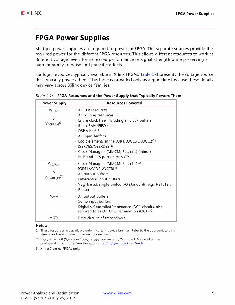
FPGA Power SuppliesMultiple power supplies are required to power an FPGA. The separate sources provide the required power for the different FPGA resources. This allows different resources to work at different voltage levels for increased performance or signal strength while preserving a high immunity to noise and parasitic effects.
For logic resources typically available in Xilinx FPGAs, Table 1-1 presents the voltage source that typically powers them. This table is provided only as a guideline because these details may vary across Xilinx device families.
Table 1-1: FPGA Resources and the Power Supply that Typically Powers Them
Power Supply Resources Powered
VCCINT
&VCCBRAM
(3)
• All CLB resources• All routing resources• Entire clock tree, including all clock buffers• Block RAM/FIFO(1)
• DSP slices(1)
• All input buffers• Logic elements in the IOB (ILOGIC/OLOGIC)(1)
• ISERDES/OSERDES(1)
• Clock Managers (MMCM, PLL, etc.) (minor)• PCIE and PCS portion of MGTs
VCCAUX
&VCCAUX_IO
(3)
• Clock Managers (MMCM, PLL, etc.)(1)
• IODELAY/IDELAYCTRL(1)
• All output buffers• Differential Input buffers• VREF-based, single-ended I/O standards, e.g., HSTL18_I• Phaser
VCCO • All output buffers • Some input buffers• Digitally Controlled Impedance (DCI) circuits, also
referred to as On-Chip Termination (OCT)(2)
MGT* • PMA circuits of transceivers
Notes: 1. These resources are available only in certain device families. Refer to the appropriate data
sheets and user guides for more information.2. VCCO in bank 0 (VCCO_0 or VCCO_CONFIG) powers all I/Os in bank 0 as well as the
configuration circuitry. See the applicable Configuration User Guide.3. Xilinx 7 series FPGAs only.
Power Analysis and Optimization www.xilinx.com 9UG907 (v2012.2) July 25, 2012
FPGA Power and the Overall Design Process
FPGA Power and the Overall Design ProcessFrom project conception to completion there are many different aspects to consider that influence power. Omitting for a moment all other constraints (functionality, performance, cost, and time to market), power related tasks can be sorted into two separate classes.
• Physical domain
Enclosure, board shape, power delivery system, thermal power dissipation system.
• Functional domain
Area, performance, I/O interfaces signal integrity.
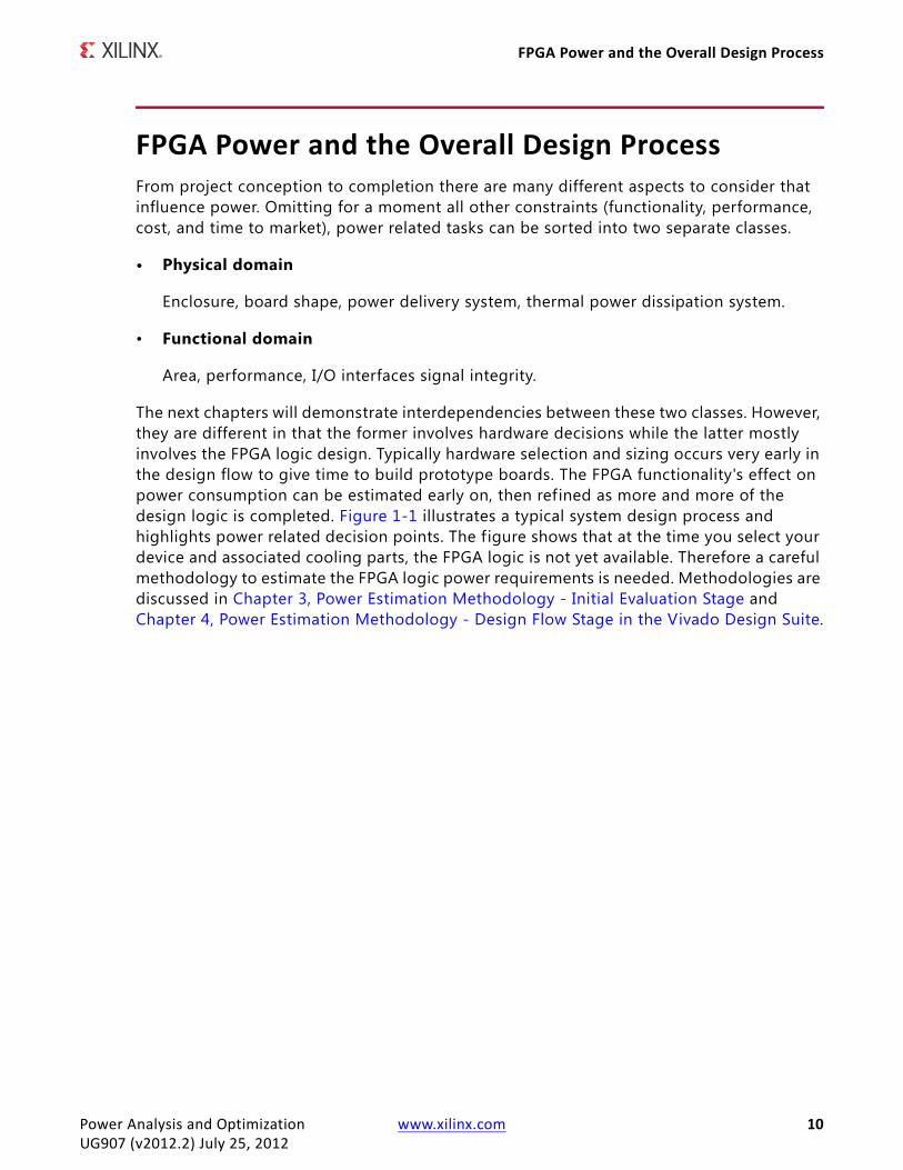
The next chapters will demonstrate interdependencies between these two classes. However, they are different in that the former involves hardware decisions while the latter mostly involves the FPGA logic design. Typically hardware selection and sizing occurs very early in the design flow to give time to build prototype boards. The FPGA functionality's effect on power consumption can be estimated early on, then refined as more and more of the design logic is completed. Figure 1-1 illustrates a typical system design process and highlights power related decision points. The figure shows that at the time you select your device and associated cooling parts, the FPGA logic is not yet available. Therefore a careful methodology to estimate the FPGA logic power requirements is needed. Methodologies are discussed in Chapter 3, Power Estimation Methodology - Initial Evaluation Stage and Chapter 4, Power Estimation Methodology - Design Flow Stage in the Vivado Design Suite.
Power Analysis and Optimization www.xilinx.com 10UG907 (v2012.2) July 25, 2012
FPGA Power and the Overall Design Process
The following chapters provide methodologies to analyze and reduce power consumption throughout the design process.
X-Ref Target - Figure 1-1
Figure 1-1: Power in the FPGA Design Process
Power Analysis and Optimization www.xilinx.com 11UG907 (v2012.2) July 25, 2012
Chapter 2
Xilinx Power Analysis Tools
IntroductionThis chapter describes the power estimation and analysis tools available for the steps in the FPGA design process. Information about device resource usage, configuration, and activity is unclear early on in the design cycle, so the software will use default values. As the design implementation progresses, more of this information can be provided to the software, which will increase the accuracy of the power estimations.
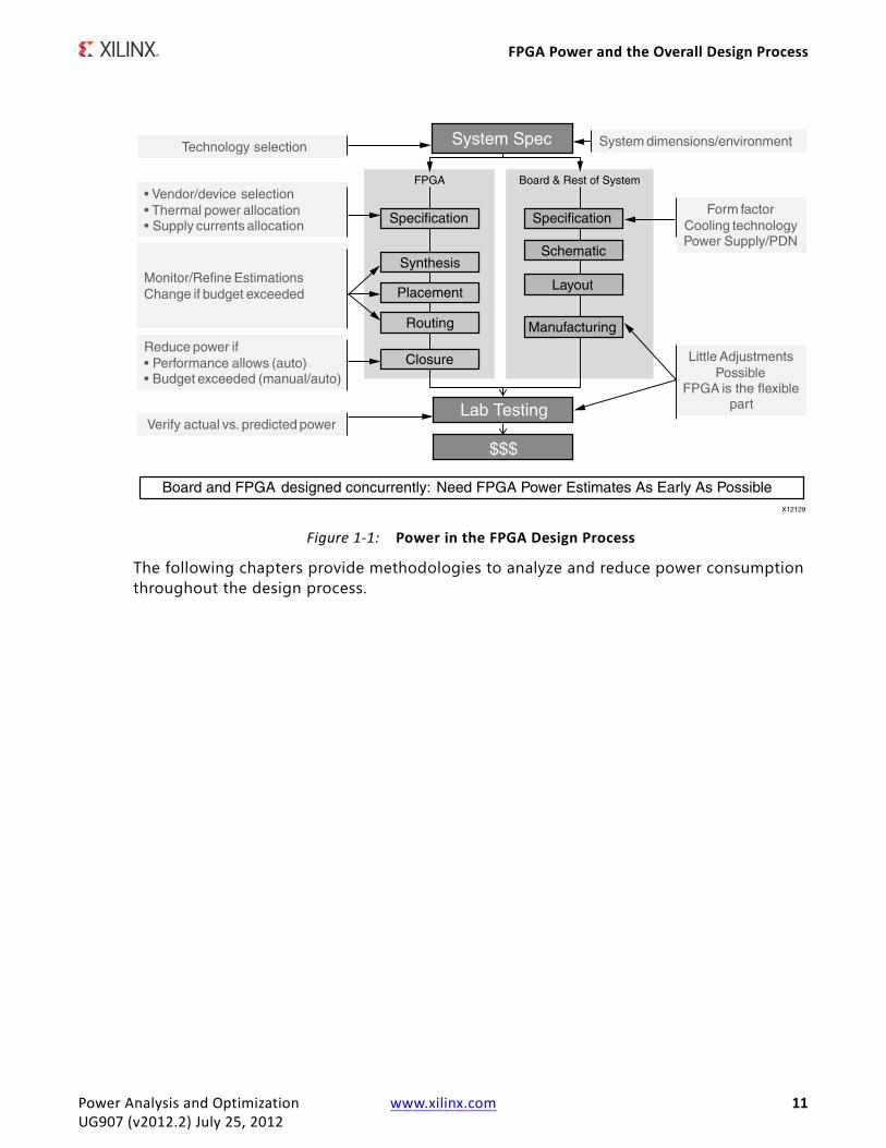
Xilinx Power Estimation and Analysis ToolsXilinx provides a suite of tools and documentation to help you evaluate the thermal and power supply requirements of your FPGA throughout the design cycle. Figure 2-1 highlights the tools available at each stage of the FPGA design cycle. Some of the tools are standalone while others are integrated into the implementation software, to align with the environment and information available to you at each stage of the design process. All the tools have communication channels so you can exchange information back and forth to be most eff icient with your analysis.
X-Ref Target - Figure 2-1
Figure 2-1: Vivado Power Estimation and Analysis Tools in the FPGA Design Process
Power Analysis and Optimization www.xilinx.com 12UG907 (v2012.2) July 25, 2012

Xilinx Power Estimation and Analysis Tools
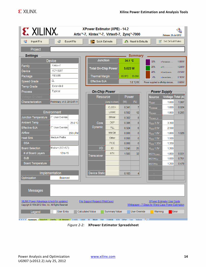
XPower Estimator (XPE)The XPower Estimator (XPE) spreadsheet is a power estimation tool typically used in the pre-design and pre-implementation phases of a project. XPE assists with architecture evaluation and device selection and helps in selecting the appropriate power supply and thermal management components which may be required for your application. The XPE interface (Figure 2-2) lets you specify design resource usage, activity rates, I/O loading, and many other factors which XPE then combines with the device models to calculate the estimated power distribution.
XPE is also commonly used later in the design cycle during implementation and power closure to, for example, evaluate power implications of engineering change orders (ECO). For large designs implemented by multiple teams, the project leader can use XPE to import utilization and activity for each team's module, then monitor the total power and reallocate the power budget to ensure constraints are met.
Power Analysis and Optimization www.xilinx.com 13UG907 (v2012.2) July 25, 2012
Xilinx Power Estimation and Analysis Tools
X-Ref Target - Figure 2-2
Figure 2-2: XPower Estimator Spreadsheet
Power Analysis and Optimization www.xilinx.com 14UG907 (v2012.2) July 25, 2012
Xilinx Power Estimation and Analysis Tools
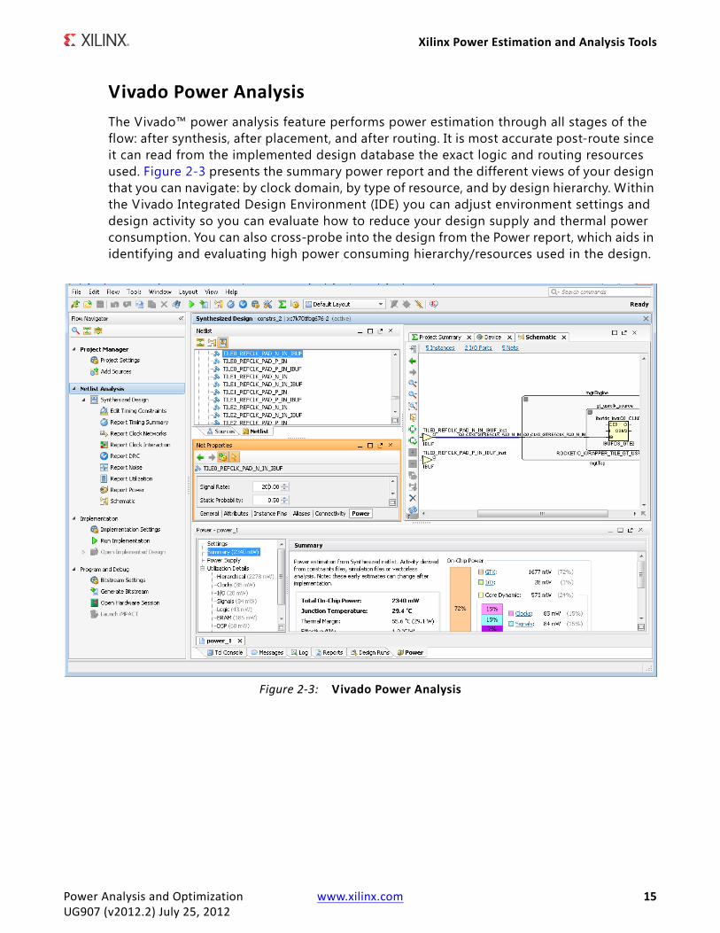
Vivado Power AnalysisThe Vivado™ power analysis feature performs power estimation through all stages of the flow: after synthesis, after placement, and after routing. It is most accurate post-route since it can read from the implemented design database the exact logic and routing resources used. Figure 2-3 presents the summary power report and the different views of your design that you can navigate: by clock domain, by type of resource, and by design hierarchy. Within the Vivado Integrated Design Environment (IDE) you can adjust environment settings and design activity so you can evaluate how to reduce your design supply and thermal power consumption. You can also cross-probe into the design from the Power report, which aids in identifying and evaluating high power consuming hierarchy/resources used in the design.
X-Ref Target - Figure 2-3
Figure 2-3: Vivado Power Analysis
Power Analysis and Optimization www.xilinx.com 15UG907 (v2012.2) July 25, 2012
User Input
User InputIn any design, users typically know the activity of specific nodes since they are imposed by the system specif ication or the interfaces with which the FPGA communicates. Providing this information to the tools, especially for nodes which drive multiple cells in the FPGA (Set, Reset, Clock Enable, or clock signals), will help guide the power estimation algorithms.
These nodes include:
• Clock Activity
Users typically know the exact frequency of all FPGA clock domains, whether externally provided (input ports), internally generated, or externally supplied to the printed circuit board (output ports).
• I/O Data Ports
With your knowledge of the exact protocols and format of the data flowing in and out of the FPGA, you can usually specify signal transition rate and/or signal percentage high rate in the tools for at least some of the I/Os. For example, some protocols have a DC balanced requirement (Signal percentage high rate =50%) or you may know how often data is written or read from your memory interface, so you can set the data rate of strobe and data signals.
• I/O and Internal Control Signals
With your knowledge of the system and the expected functionality you may be able to predict the activity on control signals such as Set, Reset and Clock Enable. These signals typically can turn on or off large pieces of the design logic, so providing this activity information will increase the power estimation accuracy.
Vector-Based EstimationIn parallel with all stages of the design development you will generally perform simulations to verify that the design behaves as expected. Different verif ication techniques are available depending on the design development state, the design complexity, or company policy. The following paragraphs highlight the valuable data you can capture and common pitfalls related to using this data to perform power analysis. An important factor for getting an accurate power estimation is that the design activity needs to be realistic. It should represent the typical or worst case scenario for data coming into the simulated block. This type of information is not necessarily provided while performing verif ication or validating functions. Sometimes invalid data is given as input to verify that the system can handle it and remain stable even when invalid data or commands are given to it. Using such test
Power Analysis and Optimization www.xilinx.com 16UG907 (v2012.2) July 25, 2012
Vector-Based Estimation
cases to perform power analysis may result in inaccurate power estimation since the design logic is not stimulated as it would be under typical system operation.
• System Transaction Level
Very early in the design cycle, you may have created a description of transactions which occur between devices on a PCB or between the different functions of your FPGA application. You can extract from this the expected activity per functional block for certain I/O ports and most of the clock domains. This information will help you f ill in the XPower Estimator spreadsheet.
• FPGA Description Level
While defining the RTL for your application you may want to verify the functionality by performing behavioral simulations. This helps you verify the data flow and the validity of calculations to the clock cycle. At this stage the exact FPGA resources used, count, and configuration is not available. You can manually extrapolate resource utilization and extract activity for I/O ports or internal control signals (Set, Reset, Clock Enable). This information can be applied to refine the XPower Estimator spreadsheet information.
Your simulator should be able to extract node activity and export it in the form of a SAIF f ile. You can save this f ile for more accurate power analysis in the Vivado design flow, for example after place and route, if you do not plan to run post-implementation simulations.
• FPGA Implementation Level
Simulation may be performed at different stages in the implementation process with different outcomes in terms of the power-related information which can be extracted. This additional information may also be used to refine the XPower Estimator spreadsheet and the Vivado power analysis as well. It may also save I/O ports and specific module activity, which can later be reused in the Vivado power analysis feature at any stage of design completion: post-synthesis, post-placement, or post-route.
° Post Synthesis: The netlist is mapped to the actual resources available in the target device.
° Post Placement: The netlist components are placed into the actual device resources. With this packing information the f inal logic resource count and configuration becomes available and you can update the XPower Estimator spreadsheet for your design.
° Post Routing: After routing is complete all the details about routing resources used and exact timing information for each path in the design are defined. In addition to verifying the implemented circuit functionality under best and worst case gate and routing delays, the simulator can also report the exact activity of internal nodes and include glitching. Power analysis at this level will provide you the most accurate power estimation before you actually measure power on your prototype board.
Power Analysis and Optimization www.xilinx.com 17UG907 (v2012.2) July 25, 2012

Vectorless Estimation
Vectorless EstimationWhen design node activity is not provided either from the user or from simulation results, the vectorless power estimation algorithms are capable of predicting this activity. The vectorless engine assigns initial “seeds” (default signal rates and static probability) to all undefined nodes. Then, starting from the design primary inputs it propagates activity to the output of internal nodes, and repeats this operation until the primary outputs are reached. The algorithm understands the design connectivity and resource functionality and configuration. Its heuristics can even approximate the glitching rate for any nodes in the netlist. Glitching occurs when design elements change states multiple times in between active clock edges before settling to a f inal value. The vectorless propagation engine is not as accurate as a post-route simulation with a reasonably long duration and realistic stimulus, but it is an excellent compromise between accuracy and compute eff iciency.
Power Analysis and Optimization www.xilinx.com 18UG907 (v2012.2) July 25, 2012
Chapter 3
Power Estimation Methodology - Initial Evaluation Stage
IntroductionThis chapter describes a methodology to evaluate your design's power consumption during the initial evaluation stage of the design cycle. You will work in XPower Estimator during this stage of the design cycle.
If you have already completed the initial evaluation stage, go to the next chapter, which describes a methodology to evaluate your design’s power consumption in the later stage of the design cycle. At this stage, you will use the Vivado™ Design Suite, which automates and simplif ies power estimation.
Initial Power Estimation in XPower Estimator
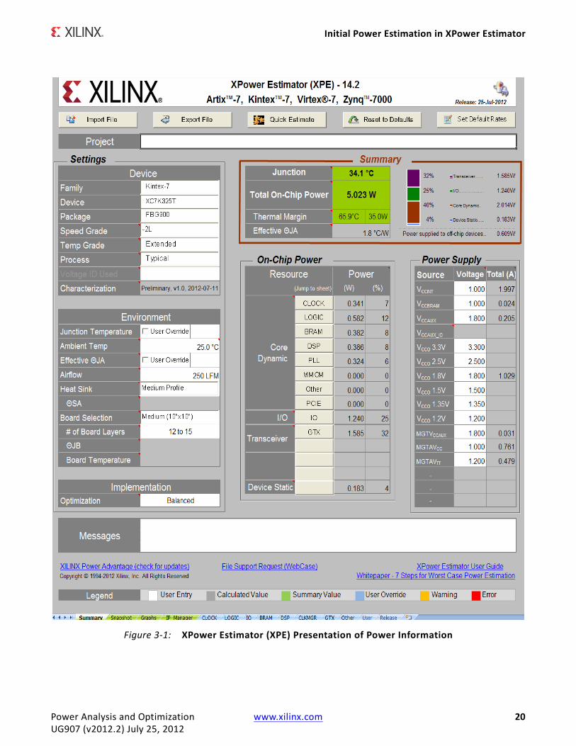
ExpectationsAt this stage you have determined that an FPGA is the most effective technology for your application. Now you need to define which vendor, family, and package can best f it your functionality, performance, cost, and power budgets. In terms of power this means that you need to estimate the total device power requirements even before any logic is developed. Understanding the total power requirements will help you define your power delivery and cooling system specif ications. Questions that you will typically ask yourself are: how many voltage supplies are needed, how much power will each be drawing, and how much of the absorbed energy will generate heat. XPower Estimator can answer these questions. It helps you develop in parallel the FPGA logic and the Printed Circuit Board on which the device will be soldered. This exercise will also help you understand the margin you can expect to have and therefore gain confidence that your system will work within budget once implemented. Figure 3-1 shows the XPower Estimator interface.
Power Analysis and Optimization www.xilinx.com 19UG907 (v2012.2) July 25, 2012
Initial Power Estimation in XPower Estimator
X-Ref Target - Figure 3-1
Figure 3-1: XPower Estimator (XPE) Presentation of Power Information
Power Analysis and Optimization www.xilinx.com 20UG907 (v2012.2) July 25, 2012
Initial Power Estimation in XPower Estimator
MethodologyAs a necessary step in any FPGA design, power and cooling specif ications need to be properly set in order to create a functioning and reliable system. In most cases, these thermal and power specif ications need to be set prior to PCB design and, due to the flexibility of FPGAs, often the FPGA design is not completed or sometimes even started prior to system design and/or PCB fabrication. This creates an interesting challenge for FPGA designers, since thermal and power characteristics can vary dramatically depending on the bitstream (design), clocking, and data put into the chip.
Underdesigning the power or thermal system can make the FPGA operate out of specification, which could result in the FPGA not operating at the expected performance or potentially other more serious consequences. Overdesigning the power system is generally less serious but still not desirable since it can add unnecessary cost and complexity to the overall FPGA design. The task of power estimation is not a trivial one prior to completing the design.
Note that these steps are primarily focused on power analysis. There are several techniques for power optimization that can be explored and applied during the analysis and can result in signif icant power savings. These techniques will be explored in the next chapter.
Step 1: Obtain the latest version of XPower Estimator for the selected target device.
It is important to make sure you are using the latest version of the XPower Estimator (XPE) tool because power information is updated periodically to reflect the latest power modeling and characterization data. The latest version of XPE can be obtained from the Xilinx® web site at http://www.xilinx.com/power. It is also helpful to check this web site occasionally during the design process to determine whether a new version has become available. If a new version is available, you can import the data from a previous version into the updated version using the Import File button on the updated version's Summary sheet. Keeping the XPower Estimator up to date ensures the most current power information will be used in the power analysis at all times during the design cycle.
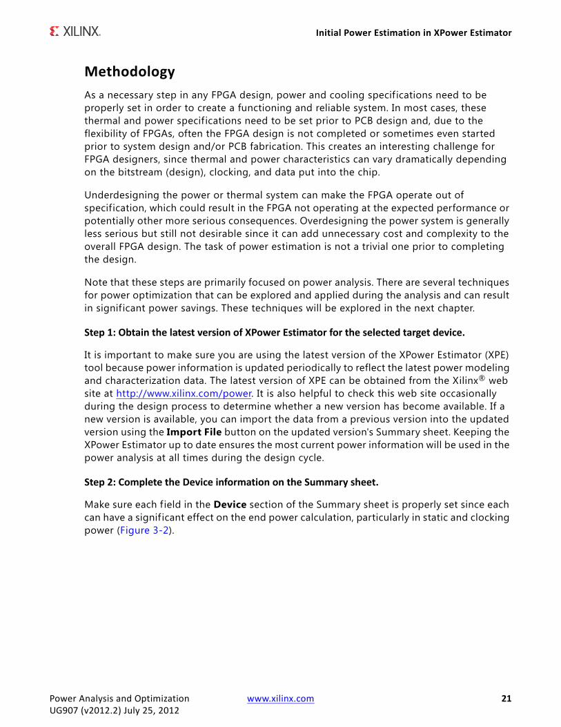
Step 2: Complete the Device information on the Summary sheet.
Make sure each f ield in the Device section of the Summary sheet is properly set since each can have a signif icant effect on the end power calculation, particularly in static and clocking power (Figure 3-2).
Power Analysis and Optimization www.xilinx.com 21UG907 (v2012.2) July 25, 2012
Initial Power Estimation in XPower Estimator
In the Device section, you will enter this information:
• Family and Device: An improperly set Family or Device can lead to incorrect device and design power estimations, such as the design power reported for clocks. It will also result in improperly reported available device resources.
• Package: The package selection can affect the device's heat dissipation and thus affect the end junction temperature. An incorrect junction temperature can result in an incorrect device static power calculation.
• Speed Grade (if available): Choose the speed grade most appropriate to the design needs. Some FPGA families may have different power specif ications for different speed grades.
• Temp Grade: Select the appropriate grade for the device (typically Commercial or Industrial). Some devices may have different device static power specifications depending on this setting. Setting this properly will also allow for the proper display of junction temperature limits for the chosen device.
X-Ref Target - Figure 3-2
Figure 3-2: Device Information - Summary Sheet
Power Analysis and Optimization www.xilinx.com 22UG907 (v2012.2) July 25, 2012
Initial Power Estimation in XPower Estimator
• Process: For the purposes of a worst-case analysis, the recommended process setting is Maximum. The default setting of Typical will give a closer picture to what would be measured statistically, but changing the setting to Maximum will modify the power specification to worst-case values.
• Voltage ID Used: The Voltage ID (VID) voltage is the minimum possible VCCINT voltage at which the FPGA can run and still meet its performance specif ications. This voltage is tested when the FPGA is manufactured and the value is programmed into the DNA eFUSE register on the FPGA. Activating the VID feature in your design to operate the FPGA at this VID voltage can result in a signif icant static power savings over operating the FPGA at its nominal voltage.
Note: This option applies to Virtex®-7, -1 speed grade, Commercial Temp grade, and Maximum Process FPGAs only.
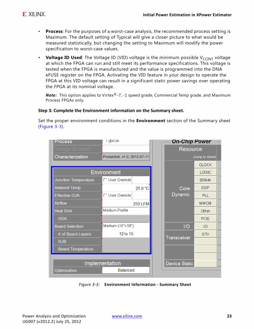
Step 3: Complete the Environment information on the Summary sheet.
Set the proper environment conditions in the Environment section of the Summary sheet (Figure 3-3).
X-Ref Target - Figure 3-3
Figure 3-3: Environment Information - Summary Sheet
Power Analysis and Optimization www.xilinx.com 23UG907 (v2012.2) July 25, 2012
Initial Power Estimation in XPower Estimator
In the Environment section, you will enter this information:
• Ambient Temp (°C): Specify the maximum possible temperature expected inside the enclosure that will house the FPGA design. This, along with airflow and other thermal dissipation paths (for example, the heatsink), will allow an accurate calculation of Junction Temperature which in turn will allow a more accurate calculation of device static power.
• Airflow (LFM): The airflow across the chip is measured in Linear Feet per Minute (LFM). LFM can be calculated from the fan output in CFM (Cubic Feet per Minute) divided by the cross sectional area through which the air passes. Specific placement of the FPGA and/or fan may have an effect on the effective air movement across the FPGA and thus the thermal dissipation. Note that the default for this parameter is 250 LFM. If you plan to operate the FPGA without active air flow (still air operation) then the 250 LFM default has to be changed to 0 LFM.
• Heat Sink (if available): If a heatsink is used and more detailed thermal dissipation information is not available, choose an appropriate profile for the type of heatsink used. This, along with other entered parameters, will be used to help calculate an effective ΘJB, resulting in a more accurate junction temperature and quiescent power calculation. Note that some types of sockets may act as heatsinks, depending on the design and construction of the socket.
• Board Selection and # of Board Layers: Selecting an approximate size and stack of the board will help calculate the effective ΘJB by taking into account the thermal conductivity of the board itself.
• ΘJB: In the event more accurate thermal modeling of the board and system is available, ΘJB (printed circuit board thermal resistance) should be used in order to specify the amount of heat dissipation expected from the FPGA.
The more accurately custom ΘJB can be specified, the more accurate the estimated junction temperature will be, thus affecting device static power calculations.
IMPORTANT: In order to specify a custom ΘJB, the Board Selection must be set to Custom. If you do specify a custom ΘJB, you must also specify a Board Temperature for an accurate power calculation.
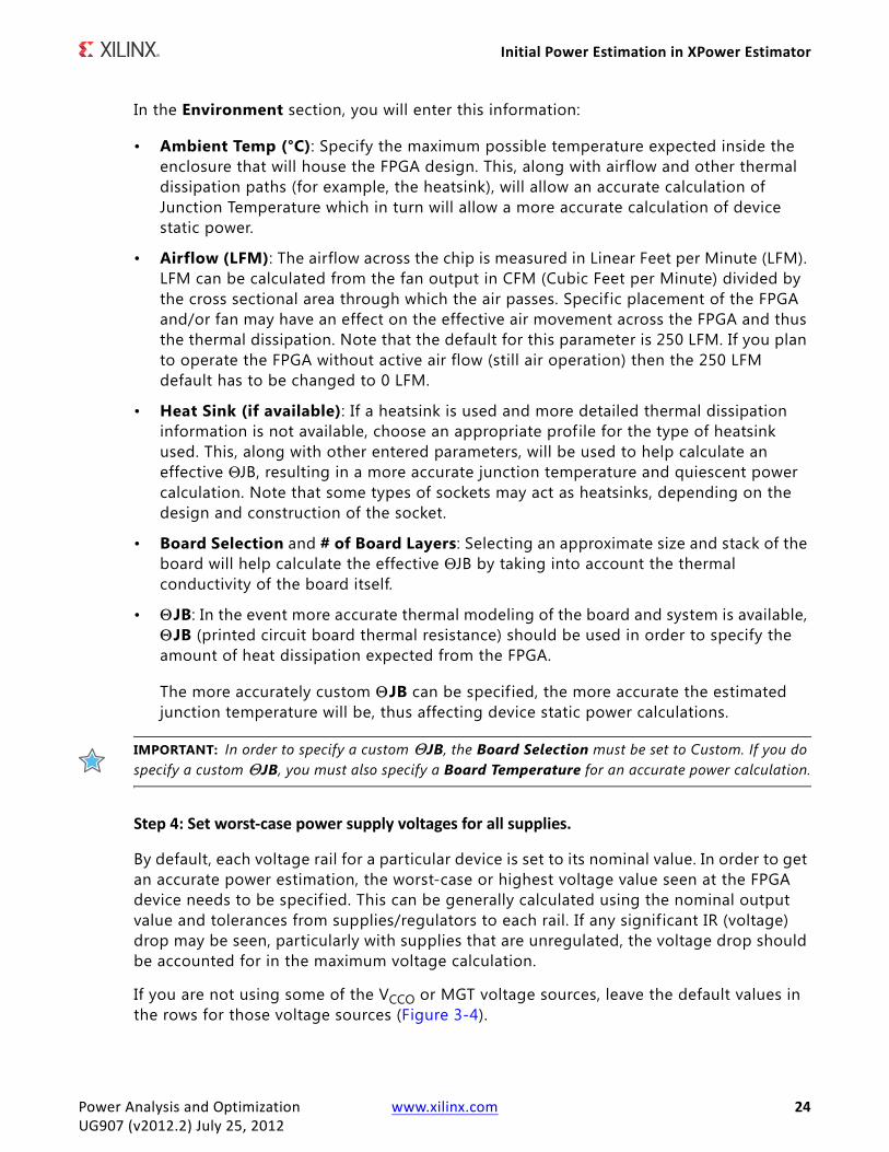
Step 4: Set worst-case power supply voltages for all supplies.
By default, each voltage rail for a particular device is set to its nominal value. In order to get an accurate power estimation, the worst-case or highest voltage value seen at the FPGA device needs to be specif ied. This can be generally calculated using the nominal output value and tolerances from supplies/regulators to each rail. If any significant IR (voltage) drop may be seen, particularly with supplies that are unregulated, the voltage drop should be accounted for in the maximum voltage calculation.
If you are not using some of the VCCO or MGT voltage sources, leave the default values in the rows for those voltage sources (Figure 3-4).
Power Analysis and Optimization www.xilinx.com 24UG907 (v2012.2) July 25, 2012
Initial Power Estimation in XPower Estimator
Step 5: Enter clock and resource information.
If the design has already been run through the Vivado tools or a previous revision of the design has been run and that revision can be used as a good starting point for the analysis, the XPower Export File (.xpe) from the design can be imported into XPE to help f ill out the resource information. To do this, use the Import File button located on the Summary sheet of XPE. Even if you do read in a Vivado XPE import f ile, quickly check to ensure the data is correct and relevant. It is best to consider importing this information as a good starting step for entering the information but not necessarily a complete solution. In any event, for each of the resource tabs, examine and if necessary fill out the expected resources to be used in the design.
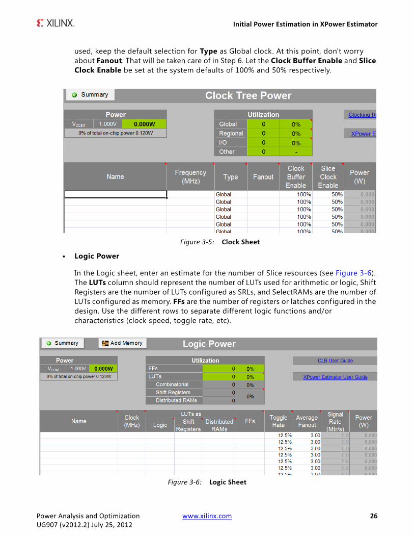
• Clock Tree Power
In the Clock sheet, enter each clock, the expected Frequency, and the expected clocking resource it will use (see Figure 3-5). If you are not certain which clocking resource will be
X-Ref Target - Figure 3-4
Figure 3-4: Power Supply Voltage Source Information - Summary Sheet
Power Analysis and Optimization www.xilinx.com 25UG907 (v2012.2) July 25, 2012
Initial Power Estimation in XPower Estimator
used, keep the default selection for Type as Global clock. At this point, don't worry about Fanout. That will be taken care of in Step 6. Let the Clock Buffer Enable and Slice Clock Enable be set at the system defaults of 100% and 50% respectively.
• Logic Power
In the Logic sheet, enter an estimate for the number of Slice resources (see Figure 3-6). The LUTs column should represent the number of LUTs used for arithmetic or logic, Shift Registers are the number of LUTs configured as SRLs, and SelectRAMs are the number of LUTs configured as memory. FFs are the number of registers or latches configured in the design. Use the different rows to separate different logic functions and/or characteristics (clock speed, toggle rate, etc).
X-Ref Target - Figure 3-5
Figure 3-5: Clock Sheet
X-Ref Target - Figure 3-6
Figure 3-6: Logic Sheet
Power Analysis and Optimization www.xilinx.com 26UG907 (v2012.2) July 25, 2012
Initial Power Estimation in XPower Estimator
In the early stages of the FPGA design, it can be diff icult to get accurate numbers for such resources, so a good suggestion is to work with large round numbers early (when the end resource count isn't well known), and as the design progresses to update the values to better represent the final representation.
TIP: When entering the clock frequency information, use Excel's capabilities to relate that cell to the cell populated in the Clock Tree Power tab. To do this, select the desired Clock (MHz) cell in the logic view, type =, and select the cell in the Clock sheet corresponding to the clock source for that logic. This should populate that cell with the value in the Clock sheet. The primary benefit of this methodology is that if the clock frequency would ever need to be changed, either by a specification change or by exploring power trade-offs vs. frequency, the value would only need to be updated in one place and can be reflected throughout the analysis. This methodology can also reduce the chance of errors and inconsistencies during the data entry.
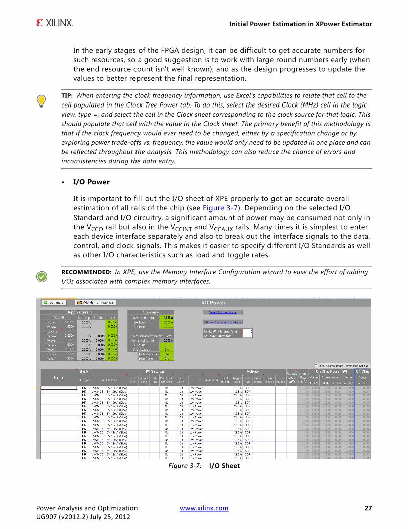
• I/O Power
It is important to fill out the I/O sheet of XPE properly to get an accurate overall estimation of all rails of the chip (see Figure 3-7). Depending on the selected I/O Standard and I/O circuitry, a significant amount of power may be consumed not only in the VCCO rail but also in the VCCINT and VCCAUX rails. Many times it is simplest to enter each device interface separately and also to break out the interface signals to the data, control, and clock signals. This makes it easier to specify different I/O Standards as well as other I/O characteristics such as load and toggle rates.
RECOMMENDED: In XPE, use the Memory Interface Configuration wizard to ease the effort of adding I/Os associated with complex memory interfaces.
X-Ref Target - Figure 3-7
Figure 3-7: I/O Sheet
Power Analysis and Optimization www.xilinx.com 27UG907 (v2012.2) July 25, 2012
Initial Power Estimation in XPower Estimator
For the I/O current calculations, the predicted power assumes standard board trace and termination is applied.
TIP: If using differential I/O each input and output should be specified as a pair. Do not specify two inputs in the spreadsheet to indicate a single differential input.
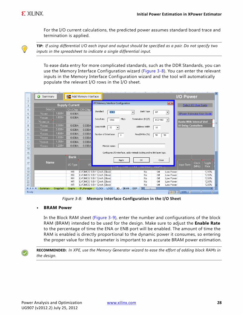
To ease data entry for more complicated standards, such as the DDR Standards, you can use the Memory Interface Configuration wizard (Figure 3-8). You can enter the relevant inputs in the Memory Interface Configuration wizard and the tool will automatically populate the relevant I/O rows in the I/O sheet.
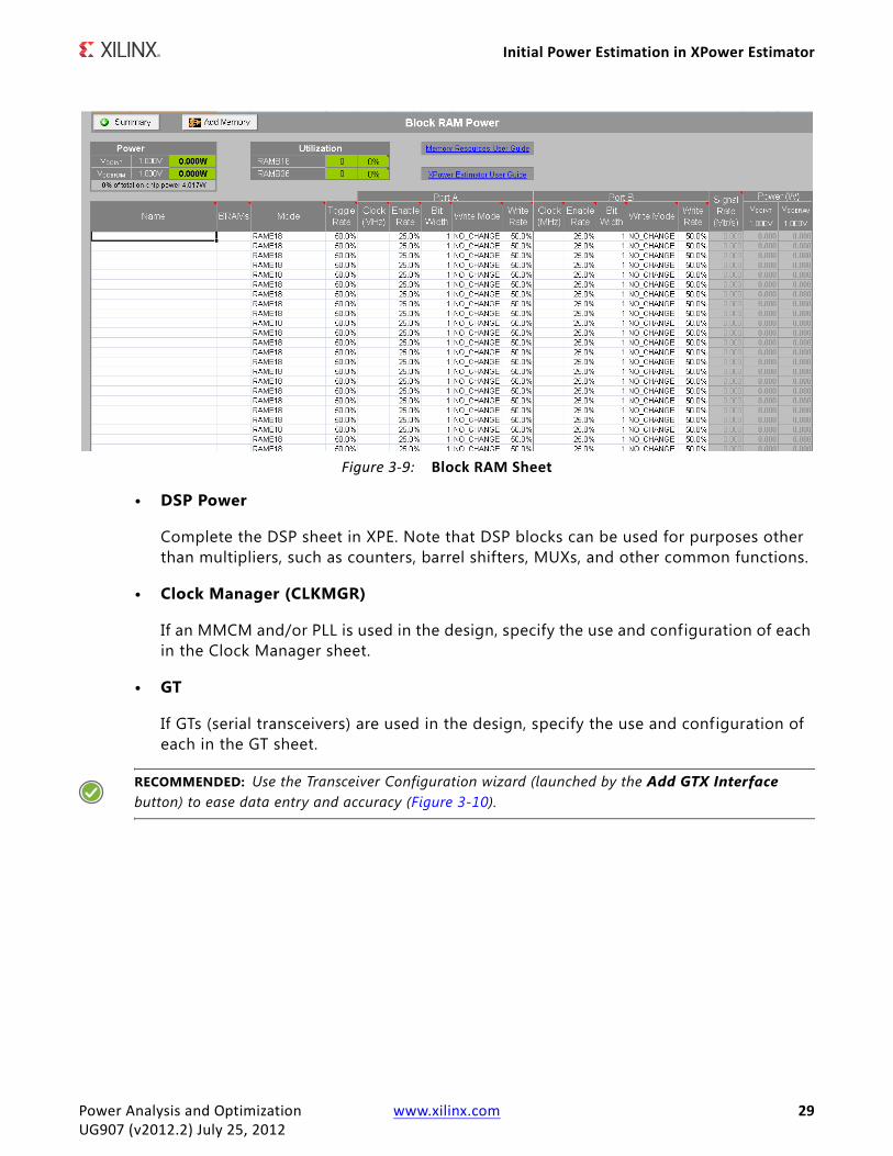
• BRAM Power
In the Block RAM sheet (Figure 3-9), enter the number and configurations of the block RAM (BRAM) intended to be used for the design. Make sure to adjust the Enable Rate to the percentage of time the ENA or ENB port will be enabled. The amount of time the RAM is enabled is directly proportional to the dynamic power it consumes, so entering the proper value for this parameter is important to an accurate BRAM power estimation.
RECOMMENDED: In XPE, use the Memory Generator wizard to ease the effort of adding block RAMs in the design.
X-Ref Target - Figure 3-8
Figure 3-8: Memory Interface Configuration in the I/O Sheet
Power Analysis and Optimization www.xilinx.com 28UG907 (v2012.2) July 25, 2012
Initial Power Estimation in XPower Estimator
• DSP Power
Complete the DSP sheet in XPE. Note that DSP blocks can be used for purposes other than multipliers, such as counters, barrel shifters, MUXs, and other common functions.
• Clock Manager (CLKMGR)
If an MMCM and/or PLL is used in the design, specify the use and configuration of each in the Clock Manager sheet.
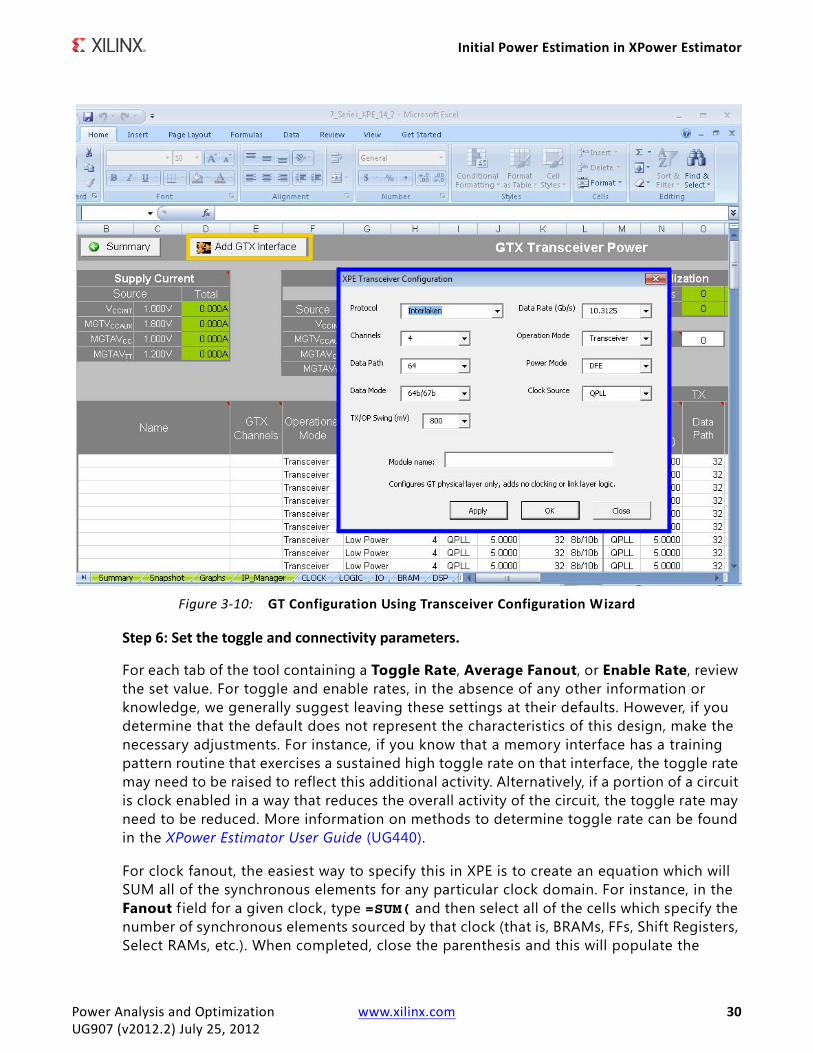
• GT
If GTs (serial transceivers) are used in the design, specify the use and configuration of each in the GT sheet.
RECOMMENDED: Use the Transceiver Configuration wizard (launched by the Add GTX Interface button) to ease data entry and accuracy (Figure 3-10).
X-Ref Target - Figure 3-9
Figure 3-9: Block RAM Sheet
Power Analysis and Optimization www.xilinx.com 29UG907 (v2012.2) July 25, 2012
Initial Power Estimation in XPower Estimator
Step 6: Set the toggle and connectivity parameters.
For each tab of the tool containing a Toggle Rate, Average Fanout, or Enable Rate, review the set value. For toggle and enable rates, in the absence of any other information or knowledge, we generally suggest leaving these settings at their defaults. However, if you determine that the default does not represent the characteristics of this design, make the necessary adjustments. For instance, if you know that a memory interface has a training pattern routine that exercises a sustained high toggle rate on that interface, the toggle rate may need to be raised to reflect this additional activity. Alternatively, if a portion of a circuit is clock enabled in a way that reduces the overall activity of the circuit, the toggle rate may need to be reduced. More information on methods to determine toggle rate can be found in the XPower Estimator User Guide (UG440).
For clock fanout, the easiest way to specify this in XPE is to create an equation which will SUM all of the synchronous elements for any particular clock domain. For instance, in the Fanout f ield for a given clock, type =SUM( and then select all of the cells which specify the number of synchronous elements sourced by that clock (that is, BRAMs, FFs, Shift Registers, Select RAMs, etc.). When completed, close the parenthesis and this will populate the
X-Ref Target - Figure 3-10
Figure 3-10: GT Configuration Using Transceiver Configuration Wizard
Power Analysis and Optimization www.xilinx.com 30UG907 (v2012.2) July 25, 2012
Initial Power Estimation in XPower Estimator
Fanout cell with the appropriate number. This method of entering clock fanout not only is often the easiest, but also has the added advantage of automatically updating when adjustments are made to the spreadsheet resource counts. The resulting Excel equation would be similar to this:
=SUM(LOGIC!E3:G3,IO!E3:G3,BRAM!C4,MULT!C3)
For logic fanout, the nature of the data and control paths need to be thought out. In designs with well structured sequential data paths, such as DSP designs, fanouts generally tend to be lower than the set default. In designs with many data execution paths, such as in some embedded designs, higher fanouts may be seen. As with toggle rates, if this information is not known it is best to leave the setting at the default and adjust later if needed.
For I/O Output Load, enter a simple capacitive load for each design output. This will affect the dynamic power of the driven output. The Output Load value is primarily made up from the sum of the individual input capacitances of each device connected to that output. The input capacitance can generally be obtained from the data sheets of the devices to which the FPGA I/O is connected.
Step 7: Analyze the results.
Before you analyze the results, update Steps 1 through 6, if necessary. After completing these steps, analyze the results. Make sure the junction temperature is not exceeded and the power drawn is within the desired budget for the project. If the thermal dissipation or power characteristics are not within targets, adjust the environmental characteristics (that is, more airflow, a heatsink, etc.) or the resource and power characteristics of the design until an acceptable result is reached. Many times, trade-offs can be made to derive the desired functionality with a tighter power budget, and the best time to explore these options is early in the design process. Once the data is completely entered and the part is operating within the thermal limits of the selected grade, the power reported by XPE can be used to specify the rails for the design. If your confidence in the data entered is not very high, you may pad the numbers to circumvent the possibility of underdesigning the power system for the FPGA. If, however, you are fairly certain of the data entered, no additional padding above the data reported by the tool is necessary.
As the design matures, continue to review and update the information in the spreadsheet to reflect the latest requirements and implementation details. This will present the most current picture of the power used in the design and could potentially allow early identif ication of adjustments to the power budgeting up or down depending on the current power trends of the design.
Refer to Chapter 4, Power Estimation Methodology - Design Flow Stage in the Vivado Design Suite, which describes a methodology to evaluate your design’s power consumption in the later stage of the design cycle, and Chapter 6, Tips and Techniques for Power Reduction for tips and tricks to reduce power in the design.
Power Analysis and Optimization www.xilinx.com 31UG907 (v2012.2) July 25, 2012
Chapter 4
Power Estimation Methodology -Design Flow Stage in the Vivado Design Suite
IntroductionThis chapter describes tool features within the Vivado™ Design Suite which automate or simplify power estimation during the design flow stage. Once you generate and analyze a power estimation within the Vivado Design Suite, go to Chapter 6, Tips and Techniques for Power Reduction for techniques to investigate and eventually modify your system, to minimize the device power consumption.
ExpectationsAs your design flow progresses through the synthesis and implementation stages you will want to monitor and verify the power consumption regularly and make sure thermal dissipation remains within budget so that you can detect and act early on if any area gets close to your constraints. The accuracy of the power estimates varies depending on the design stage when the power was estimated.
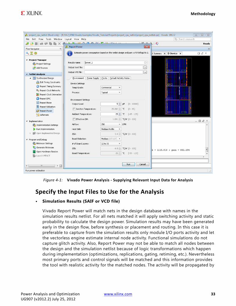
MethodologyThis section covers power analysis using Report Power in the Vivado IDE. We assume this is the f irst time you are setting up a power analysis after Synthesis. You will therefore provide the tool with the relevant activity information. For subsequent runs, you can choose whether to use Report Power in the Vivado IDE to navigate your Power report or use the Tcl equivalent (report_power) to bypass the Vivado IDE and review the text power report directly.
Power Analysis and Optimization www.xilinx.com 32UG907 (v2012.2) July 25, 2012
Methodology
Specify the Input Files to Use for the Analysis• Simulation Results (SAIF or VCD file)
Vivado Report Power will match nets in the design database with names in the simulation results netlist. For all nets matched it will apply switching activity and static probability to calculate the design power. Simulation results may have been generated early in the design flow, before synthesis or placement and routing. In this case it is preferable to capture from the simulation results only module I/O ports activity and let the vectorless engine estimate internal node activity. Functional simulations do not capture glitch activity. Also, Report Power may not be able to match all nodes between the design and the simulation netlist because of logic transformations which happen during implementation (optimizations, replications, gating, retiming, etc.). Nevertheless most primary ports and control signals will be matched and this information provides the tool with realistic activity for the matched nodes. The activity will be propagated by
X-Ref Target - Figure 4-1
Figure 4-1: Vivado Power Analysis - Supplying Relevant Input Data for Analysis
Power Analysis and Optimization www.xilinx.com 33UG907 (v2012.2) July 25, 2012

Methodology
the vectorless engine onto the unmatched design portion and increase the accuracy of the power estimation.
When you provide simulation results, make sure to use this type of simulation results:
° Ensure test vectors and inputs to the simulation represent the typical or expected behavior of the design. Error handling and corner case simulations do not typically stimulate the logic in the way it would be stimulated under normal operation.
° Post-implementation simulation results are preferred over behavioral simulation results.
IMPORTANT: Use the read_saif Tcl command to read an SAIF simulation output file and annotate matched netlist elements with the switching activity described in the file.
IMPORTANT: Use the read_vcd Tcl command to read a VCD simulation output file and annotate matched netlist elements with the switching activity described in the file.
• Known elements
This step is very important for calculating the design dynamic power since your specif ic knowledge of the application behavior can help define the activity of nodes undefined in any of the input files.
° I/O Activity
If you know the data patterns of your I/O interfaces specify this activity (Signal Rate and Static Probability (% High)) in the Power Properties window in the Vivado IDE or using the Tcl command set_switching_activity. Unless you are calculating the total power per supply in a separate tool, such as a spreadsheet, specify the termination technique for your outputs so Report Power can include the amount of power the FPGA supplies to these external components.
° Control Signals Activity
Report Power extracts and lists all the different control signals in the Signal view. You may know from the expected behavior of your application that some Set/Reset signals are not active in normal design operation so you may want to adjust the activity for these signals. Similarly, some signals in your application may disable entire blocks of the design when the blocks are not in use. Adjust their activity according to the expected functionality. Since synthesis tool and place and route algorithms can infer or remap control signals to optimize your RTL description, many of the signals listed in these views will be unfamiliar to you. When unsure of what these signals are, let the tool determine the activity.
For details on how to set the I/O Activity and Control Signals Activity values, see Performing “What If?” Analysis from the Vivado IDE in Chapter 5.
Power Analysis and Optimization www.xilinx.com 34UG907 (v2012.2) July 25, 2012
Methodology
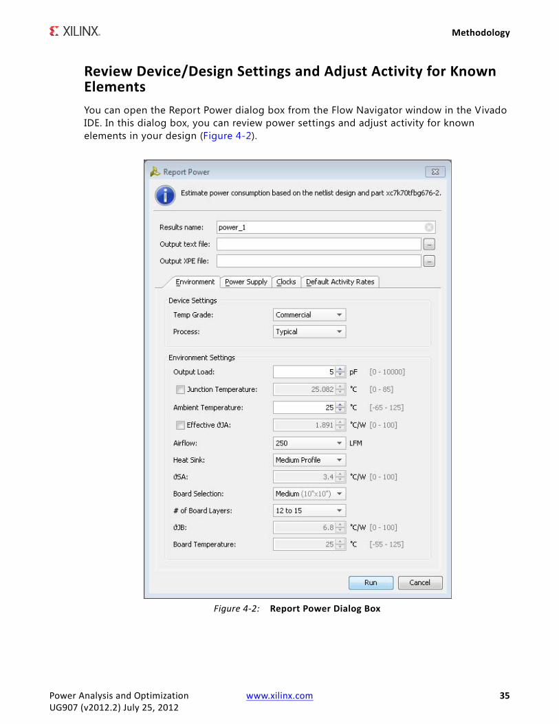
Review Device/Design Settings and Adjust Activity for Known ElementsYou can open the Report Power dialog box from the Flow Navigator window in the Vivado IDE. In this dialog box, you can review power settings and adjust activity for known elements in your design (Figure 4-2).
X-Ref Target - Figure 4-2
Figure 4-2: Report Power Dialog Box
Power Analysis and Optimization www.xilinx.com 35UG907 (v2012.2) July 25, 2012
Methodology
• Output text file
For project documentation you may want to save the power estimation results. In other circumstances you may be experimenting with different mapping, placement, and routing options to close on performance or area constraints. Saving power results for each experiment will help you select the most power-effective solution when several experiments meet your requirements.
• Output XPE file (for XPower Estimator)
Saves all environment information, device usage, and design activity in a file (.xpe) which you can later import into the XPower Estimator spreadsheet. This proves quite useful when your power budget is exceeded and you don't think that software optimization features alone will be able to meet your budgets. In this case, import the current implementation results into XPower Estimator, explore different mapping, gating, folding, and other strategies, and estimate their impact on power before modifying the RTL code or rerunning the implementation. You can also compare your assumptions in the XPower Estimator spreadsheet with these synthesis results and adjust XPE where appropriate.
Review the different input tabs to make sure they accurately represent your expected system.
• Environment: Review the different user-editable selections in the Environment tab. Make sure the process, voltage and environment data closely match your expected environment. These settings have a significant influence on the total estimated power.
The user-editable selections in the Environment tab are:
Device Settings
- Temp Grade: Select the appropriate grade for the device (typically Commercial or Industrial). Some devices may have different device static power specifications depending on this setting. Setting this properly will also allow for the proper display of junction temperature limits for the chosen device.
- Process: For the purposes of a worst-case analysis, the recommended process setting is Maximum. The default setting of Typical will give a closer picture to what would be measured statistically, but changing the setting to Maximum will modify the power specif ication to worst-case values.
Environment Settings
- Output Load (pF): The board and other external capacitance driven by the outputs in the IO ports.
- Ambient Temperature (°C): Specify the maximum possible temperature expected inside the enclosure that will house the FPGA design. This, along with airflow and other thermal dissipation paths (for example, the heatsink), will
Power Analysis and Optimization www.xilinx.com 36UG907 (v2012.2) July 25, 2012
Methodology
allow an accurate calculation of Junction Temperature which in turn will allow a more accurate calculation of device static power.
- Airflow (LFM): The airflow across the chip is measured in Linear Feet per Minute (LFM). LFM can be calculated from the fan output in CFM (Cubic Feet per Minute) divided by the cross sectional area through which the air passes. Specif ic placement of the FPGA and/or fan may have an effect on the effective air movement across the FPGA and thus the thermal dissipation. Note that the default for this parameter is 250 LFM. If you plan to operate the FPGA without active air flow (still air operation) then the 250 LFM default has to be changed to 0 LFM.
- Heat Sink (if available): If a heatsink is used and more detailed thermal dissipation information is not available, choose an appropriate profile for the type of heatsink used. This, along with other entered parameters, will be used to help calculate an effective ΘJB, resulting in a more accurate junction temperature and quiescent power calculation. Note that some types of sockets may act as heatsinks, depending on the design and construction of the socket.
- Board Selection and # of Board Layers (if available): Selecting an approximate size and stack of the board will help calculate the effective ΘJB by taking into account the thermal conductivity of the board itself.
- ΘJB: In the event more accurate thermal modeling of the board and system is available, ΘJB (printed circuit board thermal resistance) should be used in order to specify the amount of heat dissipation expected from the FPGA.
Note: In order to specify a custom ΘJB, the Board Selection must be set to Custom. If you do specify a custom ΘJB, you must also specify a Board Temperature for an accurate power calculation.
The more accurately custom ΘJB can be specif ied, the more accurate the estimated junction temperature will be, thus affecting device static power calculations.
• Default Activity Rates: In the Default Activity Rates tab review the tool's current defaults, estimate if your application departs significantly from these numbers, and decide if adjustments are required. By default, Xilinx® recommends leaving these settings unchanged since they were derived from a suite of representative user designs. These numbers are used as "seeds" for any node for which the user did not provide activity through GUI edits or an input file. The propagation engine will then adjust each node's activity depending on the activity propagated from the driving cone of logic.
• Power Supply: If this information is known, in the Power Supply tab make sure all voltage levels are set correctly for the different supply sources. Voltage is a large factor contributing to both static and dynamic power.
Power Analysis and Optimization www.xilinx.com 37UG907 (v2012.2) July 25, 2012
Methodology
• Clocks:
° Make sure all clocks are specif ied. Although not recommended, sometimes users over-constrain their designs to make the implementation tools work harder and to have more timing margin. For power calculation purposes you will want to use the exact clock frequencies your design will run on the board; otherwise the accuracy of the design dynamic power will be lower.
° Clicking Show Constrained Clocks will list all the clocks that are constrained in the design. Review the clock frequencies and ensure they are accurate.
Run the AnalysisOnce you have provided Report Power with the relevant input data, run the analysis. The tool will start by annotating the netlist with activity from files and user inputs, then apply the tool defaults for the remaining undefined nodes. Next, through an iterative process it will propagate this initial activity from the primary inputs to the primary outputs of your design to refine the activity estimate for the undefined nodes. Finally, it will calculate the dynamic power for each resource used and deduce the additional static power this switching activity generates, to compute the expected junction temperature and total power requirements for the design.
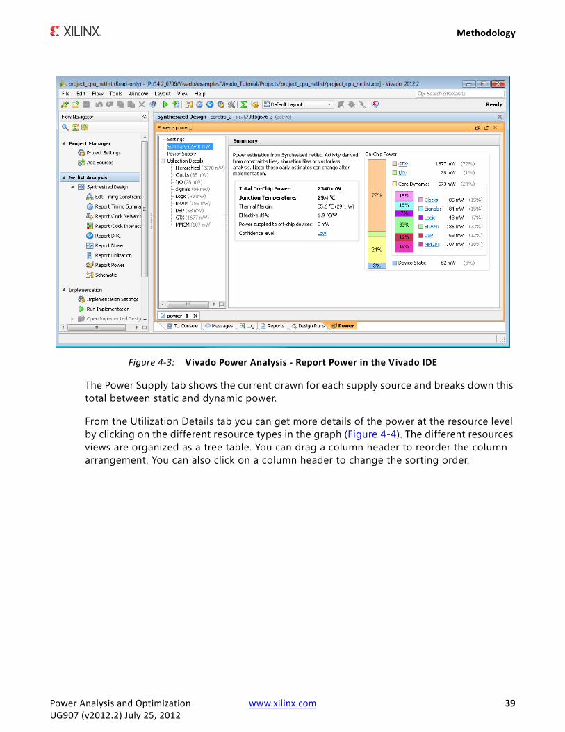
Review Your Design Power DistributionOnce the power analysis is complete you can view the Summary view to review the Total On-Chip Power and thermal properties. The On-Chip Power graph shows the power dissipated in each of the device resource types. With this high-level view you can determine which parts of your design contribute most to the total power (Figure 4-3).
Power Analysis and Optimization www.xilinx.com 38UG907 (v2012.2) July 25, 2012
Methodology
The Power Supply tab shows the current drawn for each supply source and breaks down this total between static and dynamic power.
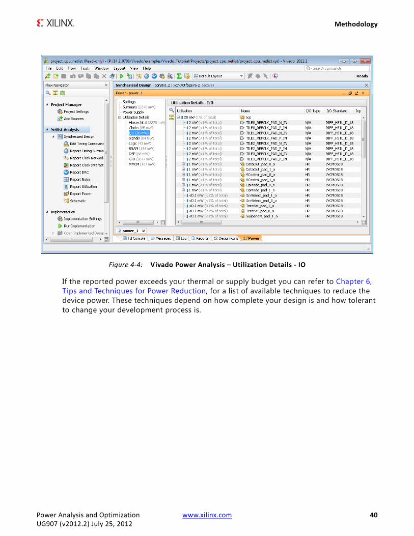
From the Utilization Details tab you can get more details of the power at the resource level by clicking on the different resource types in the graph (Figure 4-4). The different resources views are organized as a tree table. You can drag a column header to reorder the column arrangement. You can also click on a column header to change the sorting order.
X-Ref Target - Figure 4-3
Figure 4-3: Vivado Power Analysis - Report Power in the Vivado IDE
Power Analysis and Optimization www.xilinx.com 39UG907 (v2012.2) July 25, 2012
Methodology
If the reported power exceeds your thermal or supply budget you can refer to Chapter 6, Tips and Techniques for Power Reduction, for a list of available techniques to reduce the device power. These techniques depend on how complete your design is and how tolerant to change your development process is.
X-Ref Target - Figure 4-4
Figure 4-4: Vivado Power Analysis – Utilization Details - IO
Power Analysis and Optimization www.xilinx.com 40UG907 (v2012.2) July 25, 2012
Chapter 5
Power Analysis and Optimization in the Vivado Design Suite
IntroductionThis chapter discusses the power-related features and flows available in the Vivado™ Design Suite to get you quickly started with power estimation, analysis, and optimization.
You can perform power analysis after synthesis, placement or routing. It is not supported after RTL elaboration.
You can perform power optimization after synthesis only.
Using either the Vivado IDE or the Tcl prompt, you can perform power analysis and optimization, and can experiment with “What If?” scenarios in a dynamic manner.
Power AnalysisThe Vivado IDE power-related capabilities enable the following estimation and analysis features throughout the implementation of your design:
• Reporting the thermal characteristics that impact the static power of the design, including:
° Thermal statistics, such as junction and ambient temperature values
° Data on board selection, including number of board layers and board temperature
° Data on the selection of airflow and the head sink profile used by the design
• Reporting the FPGA current requirements from the different power supply sources
• Allowing detailed power distribution analysis to guide power saving strategies to reduce dynamic, thermal or off-chip power
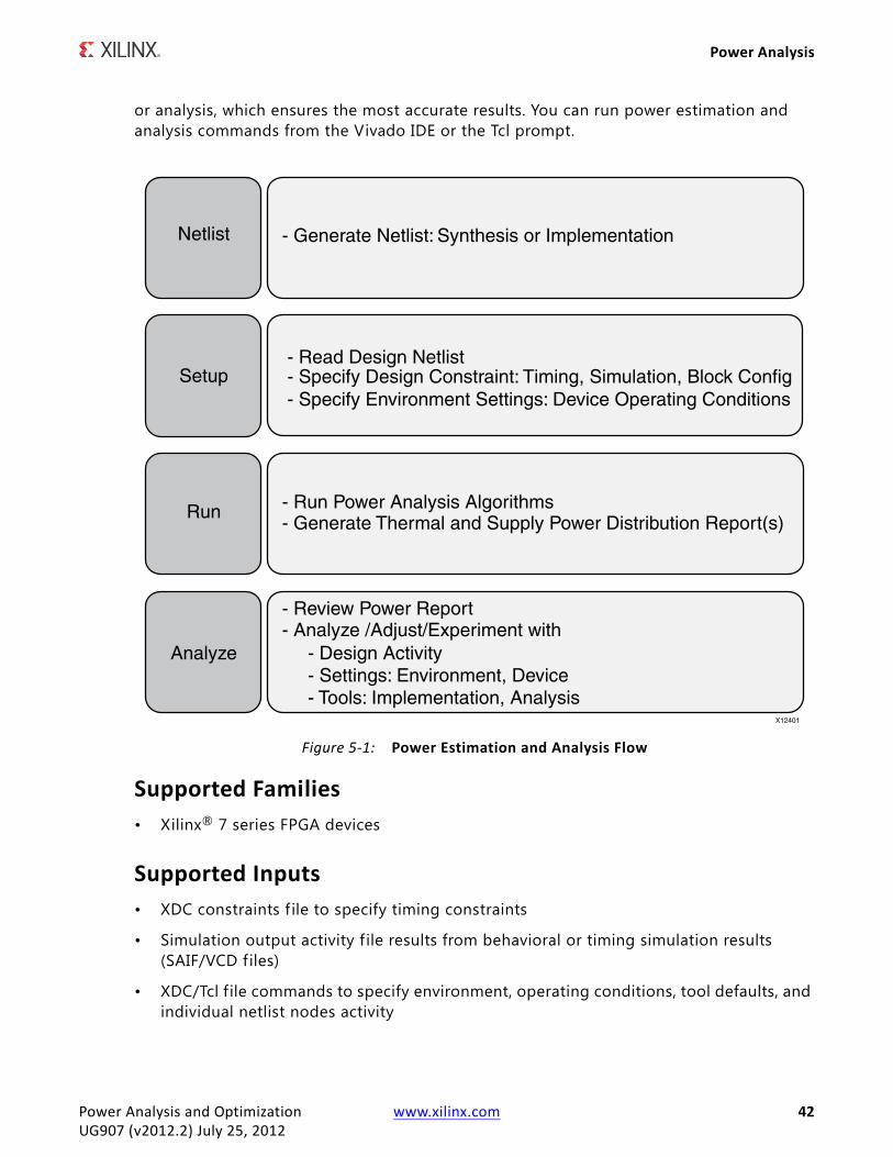
Figure 5-1 shows the typical power estimation and analysis flow. This includes the main steps required to ensure appropriate tool input and settings before running the estimation
Power Analysis and Optimization www.xilinx.com 41UG907 (v2012.2) July 25, 2012
Power Analysis
or analysis, which ensures the most accurate results. You can run power estimation and analysis commands from the Vivado IDE or the Tcl prompt.
Supported Families• Xilinx® 7 series FPGA devices
Supported Inputs• XDC constraints f ile to specify timing constraints
• Simulation output activity f ile results from behavioral or timing simulation results (SAIF/VCD files)
• XDC/Tcl f ile commands to specify environment, operating conditions, tool defaults, and individual netlist nodes activity
X-Ref Target - Figure 5-1
Figure 5-1: Power Estimation and Analysis Flow
Power Analysis and Optimization www.xilinx.com 42UG907 (v2012.2) July 25, 2012
Power Analysis
Supported Outputs• GUI and text power reports
• Tcl commands to get utilization and statistics for the specif ied netlist elements
• Open netlist in the different Vivado IDE views for more analysis
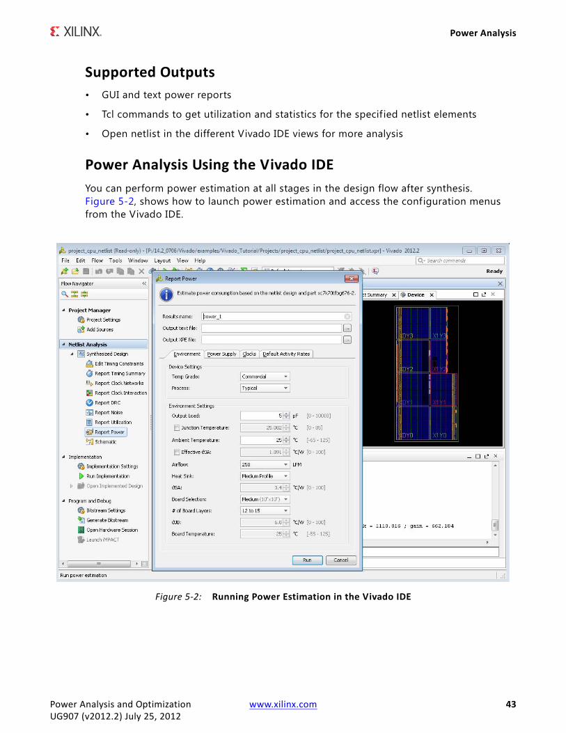
Power Analysis Using the Vivado IDEYou can perform power estimation at all stages in the design flow after synthesis. Figure 5-2, shows how to launch power estimation and access the configuration menus from the Vivado IDE.
X-Ref Target - Figure 5-2
Figure 5-2: Running Power Estimation in the Vivado IDE
Power Analysis and Optimization www.xilinx.com 43UG907 (v2012.2) July 25, 2012

Power Analysis
Setting Up Power Analysis from the Vivado IDETo specify the environment, activity, supply, and tool defaults in the Power Analysis window. See Figure 5-2.
1. Select Flow > Open Synthesized Design or Flow > Open Implemented Design.
Alternatively, you can make this selection in the Flow Navigator.
2. Select Tools > Report Power.
Alternatively, you can select Report Power in the Flow Navigator.
3. In the Report Power dialog box, adjust device environment and tool settings.
° Navigating the different tabs in the Report Power dialog box adjusts all settings to closely match your environment.
° Environment and voltage settings have a large influence on device static power.
° Activity rates and voltage settings largely influence dynamic power calculations.
° When unsure of a particular setting, use the default value.
° If you have an activity f ile from simulation results, you can specify it in this dialog box.
For more information on these settings, see Review Device/Design Settings and Adjust Activity for Known Elements in Chapter 4.
4. Specify the name of the report.
Running Power Analysis from the Vivado IDEClick Run to start the power analysis. The tool does the following:
1. Takes into account the environment, device, and tool options.
2. Reads the netlist connectivity and configuration.
3. Applies activity factors for the nodes you defined.
A node is a component such as a net, pin, or port.
4. Determines activity for any remaining undefined nodes before computing the thermal and supply power.
Power analysis uses different sources of information for activity definition, including:
• Simulation files (SAIF/VCD)
• Automatic calculations using a vectorless power analysis methodology
Power Analysis and Optimization www.xilinx.com 44UG907 (v2012.2) July 25, 2012
Power Analysis
• Manual definition using the set_switching_activity Tcl command.
For more information, see Running Power Analysis from the Tcl Prompt.
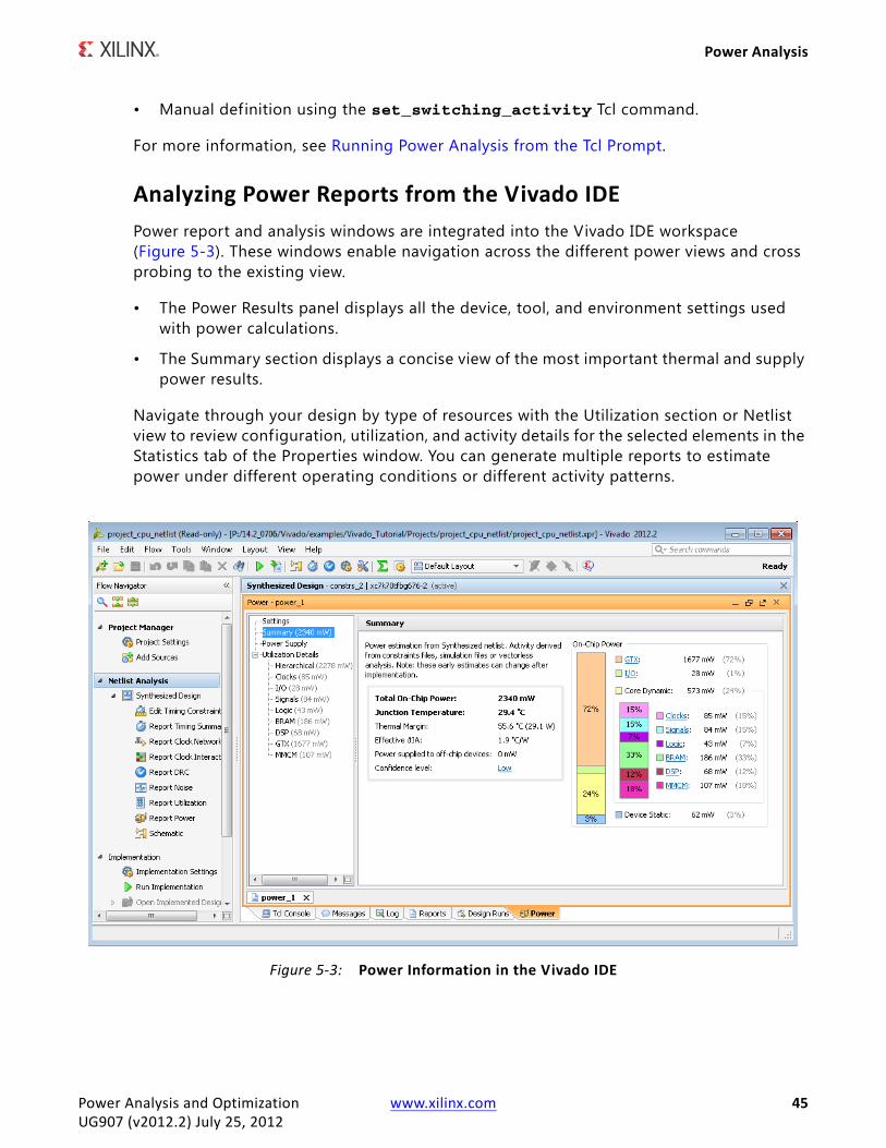
Analyzing Power Reports from the Vivado IDEPower report and analysis windows are integrated into the Vivado IDE workspace (Figure 5-3). These windows enable navigation across the different power views and cross probing to the existing view.
• The Power Results panel displays all the device, tool, and environment settings used with power calculations.
• The Summary section displays a concise view of the most important thermal and supply power results.
Navigate through your design by type of resources with the Utilization section or Netlist view to review configuration, utilization, and activity details for the selected elements in the Statistics tab of the Properties window. You can generate multiple reports to estimate power under different operating conditions or different activity patterns.
X-Ref Target - Figure 5-3
Figure 5-3: Power Information in the Vivado IDE
Power Analysis and Optimization www.xilinx.com 45UG907 (v2012.2) July 25, 2012
Power Analysis
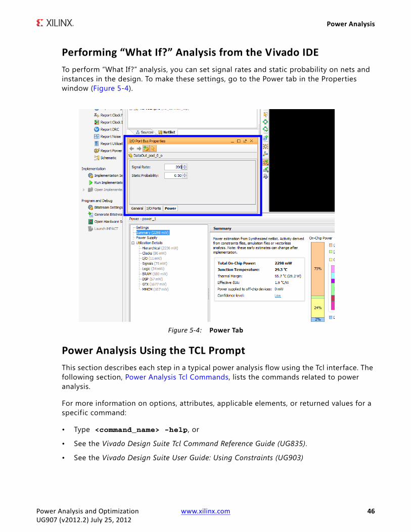
Performing “What If?” Analysis from the Vivado IDETo perform “What If?” analysis, you can set signal rates and static probability on nets and instances in the design. To make these settings, go to the Power tab in the Properties window (Figure 5-4).
Power Analysis Using the TCL PromptThis section describes each step in a typical power analysis flow using the Tcl interface. The following section, Power Analysis Tcl Commands, lists the commands related to power analysis.
For more information on options, attributes, applicable elements, or returned values for a specific command:
• Type <command_name> -help, or
• See the Vivado Design Suite Tcl Command Reference Guide (UG835).
• See the Vivado Design Suite User Guide: Using Constraints (UG903)
X-Ref Target - Figure 5-4
Figure 5-4: Power Tab
Power Analysis and Optimization www.xilinx.com 46UG907 (v2012.2) July 25, 2012
Power Analysis
Power Analysis Tcl Commands
• read_saif
• set_switching_activity
• set_default_switching_activity
• set_operating_conditions
• read_vcd
• report_switching_activity
• reset_default_switching_activity
• report_operating_conditions
• report_power
• reset_switching_activity
• report_default_switching_activity
• reset_operating_conditions
• set_units
Setting Up Power Analysis from the TCL PromptBefore running power estimations, you must provide the tool with information about the device environment and the known switching activity rates for the design netlist. This ensures the accuracy of the power estimation.
• Device Environment
• Netlist Element Activity
• Minimum Input Set
Device Environment
Specify all device operating conditions settings such as:
• Thermal, for example:
° Ambient temperature
° Heat sink
• Voltage, for example:
° VCCINT
° VCCAUX
° VCCO
Power Analysis and Optimization www.xilinx.com 47UG907 (v2012.2) July 25, 2012
Power Analysis
• Device, for example:
° Temperature grade
° Process corner
Use the following commands:
• report_operating_conditions
Report all or the specif ied operating condition settings.
• set_operating_conditions
Modify the specif ied operating condition parameters.
• reset_operating_conditions
Return all or the specif ied operating condition parameters to the default values for the selected device.
Netlist Element Activity
Use the following commands to define the switching activity, including signal rate and static probability, and the clock waveform information for known netlist elements.
• report_switching_activity
° Reports the activity of the specified elements.
° Returns the average activity when multiple elements are specif ied.
• set_switching_activity
Set the activity of the specif ied elements.
• reset_switching_activity
Reset the specified netlist elements activity to the tool default.
• report_default_switching_activity
Report the default activity of the specif ied default types.
• set_default_switching_activity
Set the activity of the specif ied default types.
• reset_default_switching_activity
Reset the activity of the specified default types.
Power Analysis and Optimization www.xilinx.com 48UG907 (v2012.2) July 25, 2012
Power Analysis
• read_saif
Read an SAIF simulation output f ile and annotate matched netlist elements with the switching activity described in the file.
• read_vcd
Read a VCD simulation output file and annotate matched netlist elements with the switching activity described in the file.
• create_clock
Synthesis and implementation constraint to specify clock waveforms.
• create_generated_clock
Synthesis and implementation constraint to specify generated clock waveforms.
By default, create_clock and create_generated_clock are defined in the XDC file and do not need to be defined again.
Minimum Input Set
Before performing power estimation:
• Make sure the activity of all clocks in your netlist is defined.
• If possible, specify the activity of all primary input ports in your design using the Tcl commands or reading a simulation output file. These port activity rates determine the internal logic activity rates. Therefore, if the tool’s default settings do not match your application, the internal logic activity may be overestimated or underestimated.
• If known, specify the activity of any high fanout nets that you defined in your HDL code, such as global set, reset, and clock enable signals.
When reading the simulation result f ile, make sure the activity is representative of the typical or worst case design activity. Using simulation results from atypical scenarios can lead to inaccurate power estimations.
Power Analysis and Optimization www.xilinx.com 49UG907 (v2012.2) July 25, 2012

Power Analysis
Running Power Analysis from the Tcl PromptAfter all environment and activity settings are defined, you can run the power analysis algorithm using the report_power command. The tool does the following:
1. Loads your environment settings and design netlist.
2. Annotates activity for any netlist element you specified with input f iles or Tcl commands.
Note: For all undefined nodes, the tool uses the vectorless propagation engine to estimate activity, taking into account activity of known elements and logic configuration and connectivity.
3. Calculates and reports the design thermal and supply power.
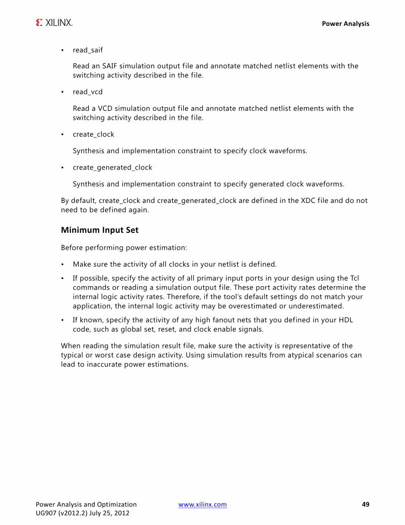
Analyzing Power Reports from the Tcl PromptTo analyze the design power, start by reviewing the total thermal and supply power information in the power report (Figure 5-5).
Then, depending on your design margin against requirements, you can review the resource or hierarchy sections. These sections show the design power distribution at a more detailed level. As a result of your analysis, you may want to return to XPower Estimator and perform design architectural scenarios.
You can also perform "What If?" scenarios to evaluate the impact of changes in the settings for:
• Environment
• Device
• Implementation
• Power tool
Power Analysis and Optimization www.xilinx.com 50UG907 (v2012.2) July 25, 2012
Power Analysis
ExamplesUsing the cpu_hdl design included with the Vivado tools, the following scripts provide examples for most of the commands discussed in the previous sections.
You can perform power reporting dynamically using Tcl commands. For example:
vivado -mode batch -source power_analysis.tcl
You can also use a Tcl script. The script examples below assume you are using the batch mode and sourcing the script.
X-Ref Target - Figure 5-5
Figure 5-5: Text Report Generated for Power and Thermal Information
Power Analysis and Optimization www.xilinx.com 51UG907 (v2012.2) July 25, 2012

Power Analysis
Example 1: Post-Synthesis and Post-Implementation Power Estimation and Comparison in Project Mode
#--------------------- Setup estimation ---------------------
# Open project with HDL source files and timing constraintsopen_project $install_directory/project_cpu_hdl/project_cpu_hdl.ppr
# Display tool default assumed operating conditionsreport_operating_conditions -all
# Set specific device and environment operating conditionsset_operating_conditions -ambient 25set_operating_conditions -voltage {vccint 0.95 vccaux 1.71}
#----------------------- Run Synthesis then Power estimation -----------------
# Run Vivado Design Suite synthesis and automaticallylaunch_runs synth_1
#open designopen_run synth_1
# Generate verbose post-synthesis power reportreport_power -verbose -file ex1_post-synthesis.pwr
#------------------------ Run Implementation then Power estimation -----------launch_runs impl_1
#open designopen_run impl _1
# Generate post-implementation verbose power reportreport_power -file ex1_post-implementation.pwr
# Return operating conditions to default for devicereset_operating_conditions -ambient -voltage {vccint vccaux} # could use '-all'
Example 2: Post-Synthesis and Post-Implementation Power Estimation and Comparison in Projectless Mode
#--------------------- Setup estimation ---------------------
# Open netlist in projectless mode read_edif -name top.edf
# read design constraintsread_xdc -name top_full.xdc
# Display tool default assumed operating conditionsreport_operating_conditions -all
# Set specific device and environment operating conditionsset_operating_conditions -ambient 25set_operating_conditions -voltage {vccint 0.95 vccaux 1.71}
Power Analysis and Optimization www.xilinx.com 52UG907 (v2012.2) July 25, 2012
Power Analysis
#----------------------- Power estimation post synthesis -----------------
# Generate verbose post-synthesis power reportreport_power -verbose -file ex1_post-synthesis.pwr
#----Run various Implementation steps then Power estimation after every step --------opt_designreport_power -verbose -file ex1_post-opt_design.pwrpower_opt_design ;# Optional report_power -verbose -file ex1_post_pwr_opt_design.pwrplace_design report_power -verbose -file ex1_post_place_design.pwrphys_opt_design ;# Optionalreport_power -verbose -file ex1_post_phys_opt_design.pwrroute_design
# Generate post-route verbose power reportreport_power -verbose -file ex1_post_route_design.pwr
# Return operating conditions to default for devicereset_operating_conditions -ambient -voltage {vccint vccaux} # could use '-all'
Example 3: Examine and ensure “% high” values on resets are accurate
# Identify resets in the design
# Query the % high value of the reset identified for the designreport_switching_activity -static_probability reset# Output is - reset: static probability = 0.5 (D)
# Set %high value of reset to 0set_switching_activity -static_probability 0.0 reset
# Generate post-route verbose power reportreport_power -verbose -file ex1_post_route_design.pwr
Example 4: Report, Modify, and Reset Tool and Device Environment Settings
Open the previously implemented design, and then enter or source the following commands. This changes the default activity settings and generates a new power report.
#------------------- Report tool default activity settings -------------------
# Show tool default activity for the different class of netlist elementsreport_default_switching_activity -type all
# Generate power report with tool default settingsreport_power -file ex2_tool-default-activity.pwr
Power Analysis and Optimization www.xilinx.com 53UG907 (v2012.2) July 25, 2012

Power Analysis
#------------------- Modify tool default activity settings -------------------
# Set default clock freq of 100 MHz for all unconstrained clocksset_default_switching_activity -toggle_rate 100 -type clock
# Increase activity of design inputs from 12.5 to 25% of clock rateset_default_switching_activity -type input -static_probability 50 -toggle_rate 25
# Report static and dynamic power implicationsreport_power -file ex2_modified-default-activity.pwr
#------------------- Reset tool default activity settings -------------------
# Return activity of design inputs to defaultreset_default_switching_activity -all
Example 5: What If? Design Analysis/Report, Edit, and Reset Design Activity
Working with power analysis can be very dynamic, allowing you to explore “What If?” scenarios on the fly. Open the previously implemented design, and enter or source the following commands. This modif ies activity for control signals (clock enable and reset) in submodule fftEngine to evaluate the impact on power for this hierarchical level and the entire design.
#---------------- Report power and activity with default settings ------------
# Report power report_power -file ex3_power_before.pwr
# Get activity of signals of interestreport_switching_activity -object_list [get_nets {fftEngine/reset fftEngine/wb_we_i_reg}]
#---------- scenario with no reset and higher CE activity --------------
# disable reset and enable clock enables in module fftEngine most of the timeset_switching_activity -static_probability 0 -object_list [get_nets fftEngine/reset]set_switching_activity -static_probability 1 -object_list [get_nets fftEngine/wb_we_i_reg]report_power -file ex3_power_no_reset_activ.pwrreport_switching_activity -object_list [get_nets fftEngine/reset fftEngine/wb_we_i_reg]
#----------- scenario with active reset and low CE activity ---------
# enable reset and disable clock enable in module fftEngine most of the timeset_switching_activity -static_probability 1 -object_list [get_nets fftEngine/reset]set_switching_activity -static_probability 0 -object_list [get_nets fftEngine/wb_we_i_reg]report_power -file ex3_power_reset_activ.pwrreport_switching_activity -object_list [get_nets fftEngine/reset fftEngine/wb_we_i_reg]
Power Analysis and Optimization www.xilinx.com 54UG907 (v2012.2) July 25, 2012
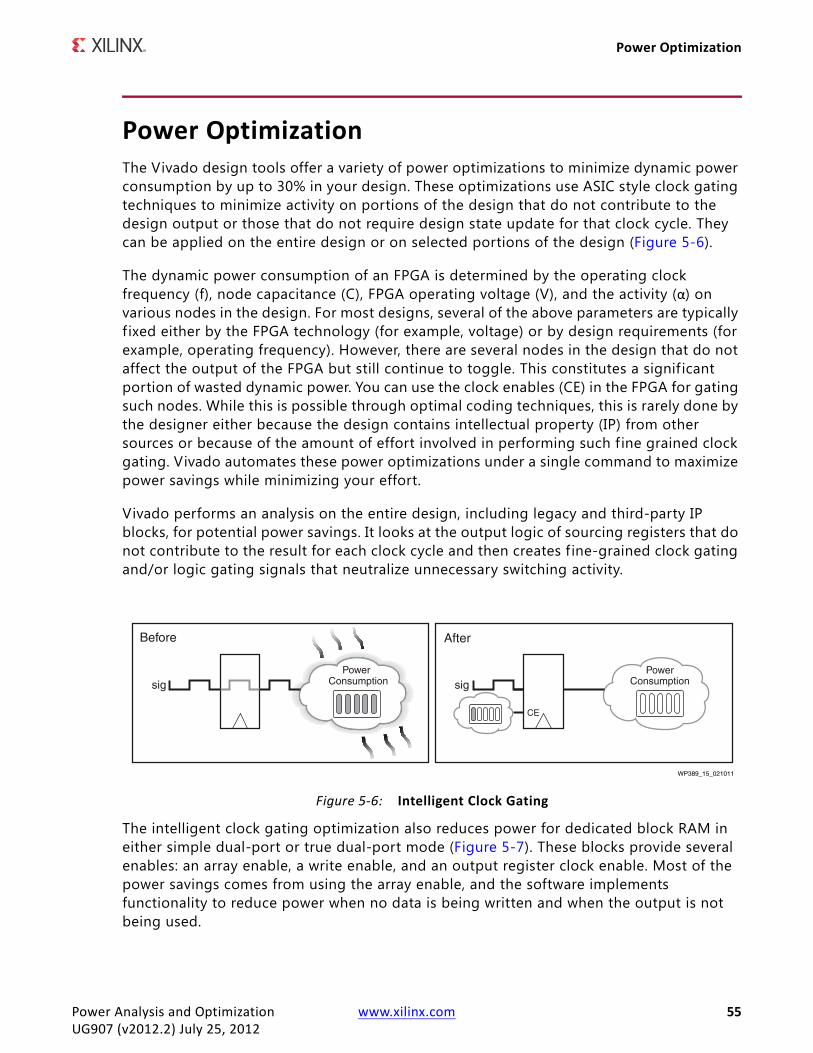
Power Optimization
Power OptimizationThe Vivado design tools offer a variety of power optimizations to minimize dynamic power consumption by up to 30% in your design. These optimizations use ASIC style clock gating techniques to minimize activity on portions of the design that do not contribute to the design output or those that do not require design state update for that clock cycle. They can be applied on the entire design or on selected portions of the design (Figure 5-6).
The dynamic power consumption of an FPGA is determined by the operating clock frequency (f), node capacitance (C), FPGA operating voltage (V), and the activity (α) on various nodes in the design. For most designs, several of the above parameters are typically f ixed either by the FPGA technology (for example, voltage) or by design requirements (for example, operating frequency). However, there are several nodes in the design that do not affect the output of the FPGA but still continue to toggle. This constitutes a signif icant portion of wasted dynamic power. You can use the clock enables (CE) in the FPGA for gating such nodes. While this is possible through optimal coding techniques, this is rarely done by the designer either because the design contains intellectual property (IP) from other sources or because of the amount of effort involved in performing such f ine grained clock gating. Vivado automates these power optimizations under a single command to maximize power savings while minimizing your effort.
Vivado performs an analysis on the entire design, including legacy and third-party IP blocks, for potential power savings. It looks at the output logic of sourcing registers that do not contribute to the result for each clock cycle and then creates f ine-grained clock gating and/or logic gating signals that neutralize unnecessary switching activity.
The intelligent clock gating optimization also reduces power for dedicated block RAM in either simple dual-port or true dual-port mode (Figure 5-7). These blocks provide several enables: an array enable, a write enable, and an output register clock enable. Most of the power savings comes from using the array enable, and the software implements functionality to reduce power when no data is being written and when the output is not being used.
X-Ref Target - Figure 5-6
Figure 5-6: Intelligent Clock Gating
Power Analysis and Optimization www.xilinx.com 55UG907 (v2012.2) July 25, 2012
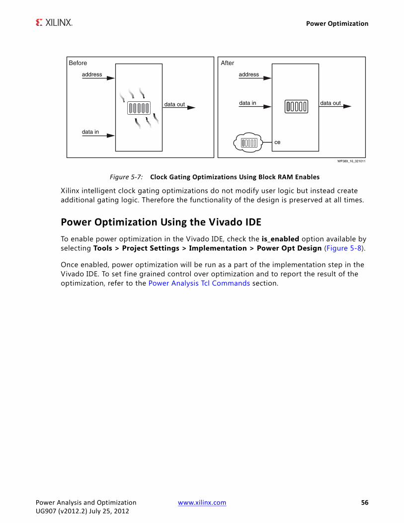
Power Optimization
Xilinx intelligent clock gating optimizations do not modify user logic but instead create additional gating logic. Therefore the functionality of the design is preserved at all times.
Power Optimization Using the Vivado IDETo enable power optimization in the Vivado IDE, check the is_enabled option available by selecting Tools > Project Settings > Implementation > Power Opt Design (Figure 5-8).
Once enabled, power optimization will be run as a part of the implementation step in the Vivado IDE. To set f ine grained control over optimization and to report the result of the optimization, refer to the Power Analysis Tcl Commands section.
X-Ref Target - Figure 5-7
Figure 5-7: Clock Gating Optimizations Using Block RAM Enables
Power Analysis and Optimization www.xilinx.com 56UG907 (v2012.2) July 25, 2012
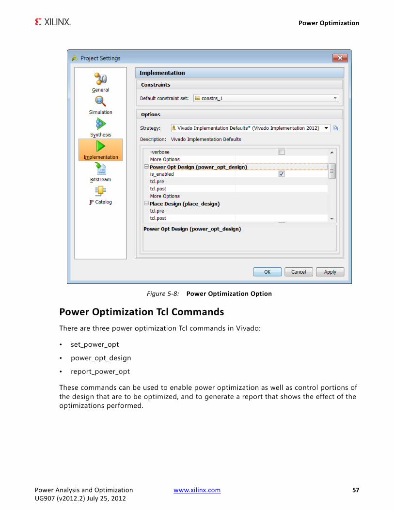
Power Optimization
Power Optimization Tcl CommandsThere are three power optimization Tcl commands in Vivado:
• set_power_opt
• power_opt_design
• report_power_opt
These commands can be used to enable power optimization as well as control portions of the design that are to be optimized, and to generate a report that shows the effect of the optimizations performed.
X-Ref Target - Figure 5-8
Figure 5-8: Power Optimization Option
Power Analysis and Optimization www.xilinx.com 57UG907 (v2012.2) July 25, 2012
Power Optimization
Setting Power Optimization Constraints
Prior to running power optimization, you can optionally set power optimization constraints to identify portions of the design that need to be optimized for power. The set_power_opt command provides you the option to include or exclude cell types, hierarchy levels or clock domains for power optimization.
TIP: You will still need to use the power_opt_design command to enable the power optimization step. The set_power_opt command is used only for targeting the optimization.
The syntax for the set_power_opt command is:
set_power_opt [-include_cells <args>] [-exclude_cells <args>] [-clocks <args>] [-cell_types <args>] [-quiet] [-verbose]
Examples
The following example sets power optimization for BRAM and REG type cells, then adds SRLs:
set_power_opt -cell_types {bram reg}set_power_opt -cell_types {srl}
The following example sets power optimization for BRAM cells only, then excludes the cpuEngine block from optimization, but then includes the cpuEngine/cpu_dbg_dat_i block:
set_power_opt -cell_types bramset_power_opt -exclude_cells cpuEngineset_power_opt -include_cells cpuEngine/cpu_dbg_dat_i
Table 5-1: set_power_opt Options
Option Name Optional Default Description
-include_cells Yes All Include only the listed instances for clock gating
-exclude_cells Yes None Exclude the listed instances from clock gating
-clocks Yes All clocks Clock gate the instances clocked by the listed clocks only
-cell_types Yes All Clock gate the following cell types only: [all|bram|reg|srl|none]
-quiet Yes N/A Ignore command errors
-verbose Yes N/A Suspend message limits during command execution
Power Analysis and Optimization www.xilinx.com 58UG907 (v2012.2) July 25, 2012
Power Optimization
Running Power Optimization
Power optimization runs post-synthesis or post-opt_design and pre-place in the flow. When enabled, the tool optimizes the entire design or portions of the design (when set_power_opt is used) for power.
A typical script would be:
synth_designopt_designpower_opt_designplace_designroute_designreport_power
The syntax for this command is:
power_opt_design [-quiet] [-verbose]
Generating a Power Optimization Report
The report_power_opt command provides you with a hierarchical breakdown of all the instances including block RAMs, SRLs, and registers that have been optimized for power. It provides information on the enables used for each instance and if the enables were created by Vivado (or by the user).
The syntax for this command is:
report_power_opt [-cell <arg>] [-file <arg>] [-quiet] [-verbose]
Table 5-2: power_opt_design Options
Option Name Optional Default Description
-quiet Yes N/A Ignore command errors
-verbose Yes N/A Suspend message limits during command execution
Table 5-3: report_power_opt Options
Option Name Optional Default Description
-cell Yes Top level Report power optimization for a specific cell
-f ile Yes None Write the report into the specified file. The specified file will be overwritten if one already exists
-quiet Yes N/A Ignore command errors
verbose Yes N/A Suspend message limits during command execution
Power Analysis and Optimization www.xilinx.com 59UG907 (v2012.2) July 25, 2012

Power Optimization
Examples
The following example creates a file named myopt.rep and reports power optimization for the entire design:
report_power_opt -file myopt.rep
The following example creates a file named myopt.rep and reports power optimization for the mctrl0 sub-hierarchy of the design:
report_power_opt -file myopt2.rep -cell mcore0/mctrl0
Using Power Optimization to Maximize Power SavingTo maximize power savings when you run power optimization in the Vivado tools, you should run power optimization on the entire design and not exclude portions of the design. If you do not see anticipated power savings after enabling power optimization, the three areas of potential debug are the global set and reset signals, block RAM enable generation, and register clock gating. A low number of power optimization generated enables in this area could indicate the need to review coding practices or options/attributes set for design synthesis and implementation.
• Global set and reset signals
Where possible, minimize the use of asynchronous set/reset signals especially to datapath or pipeline flip-flops as well as block RAMs (BRAM).
You should also consider constraining the global set and reset signals as dont_touch during the power_opt_design step to avoid their use as enables. Note that setting dont_touch attribute in HDL will cause every step in the flow to obey this property. It is recommended that this option is set up as an XDC constraint only for the power optimization step. Here is an example of how to do this:
set_property DONT_TOUCH true [get_cells u1]
Finally, ensure that the signal rate and probabilities of the global set and reset signals are set correctly prior to running power optimization and vectorless power estimation.
• Slice registers and SRLs
A number of different reasons could explain why power_opt_design might not be able to generate clock enables for slice registers or SRLs in the design. Some examples are:
° Having combinatorial loops in the design
° Using set/reset signals at the flip-flops and SRLs that are sourced from primary inputs to the design
° Using asynchronous set/reset signals at the datapath flip-flops
Power Analysis and Optimization www.xilinx.com 60UG907 (v2012.2) July 25, 2012
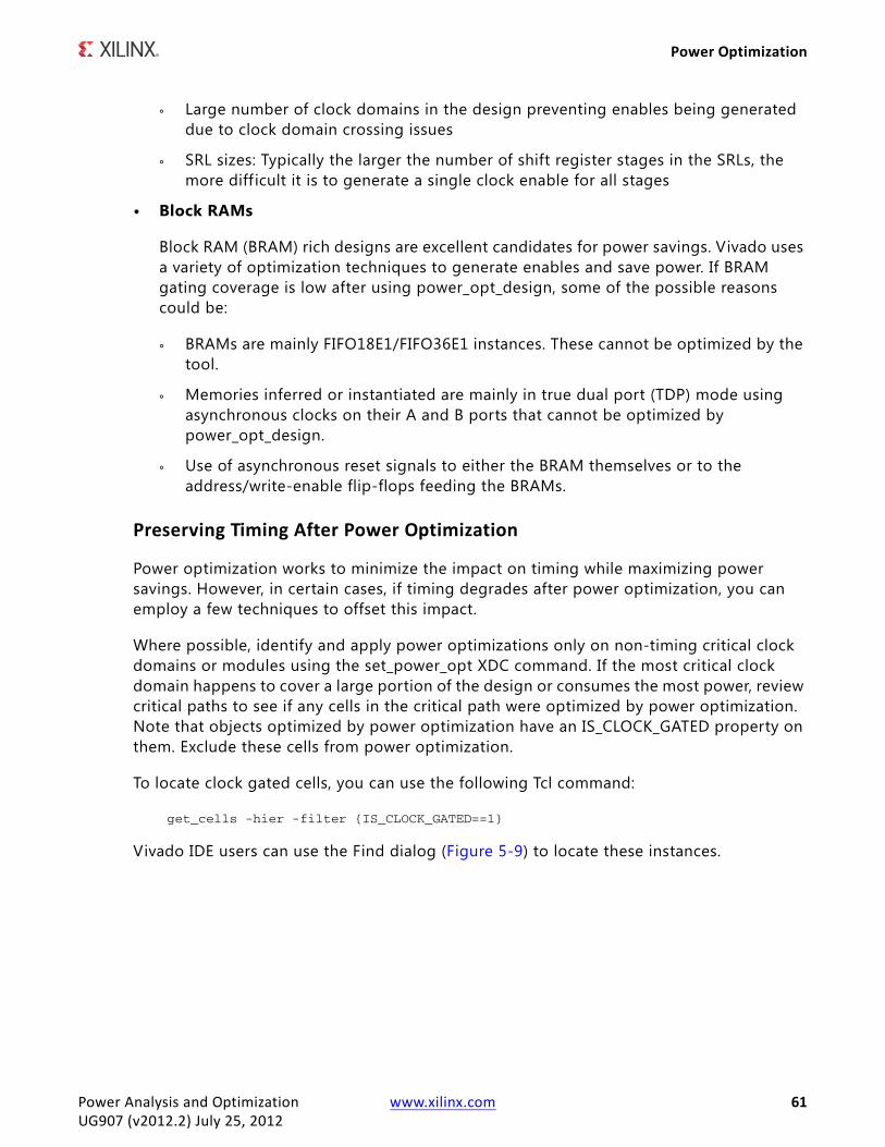
Power Optimization
° Large number of clock domains in the design preventing enables being generated due to clock domain crossing issues
° SRL sizes: Typically the larger the number of shift register stages in the SRLs, the more diff icult it is to generate a single clock enable for all stages
• Block RAMs
Block RAM (BRAM) rich designs are excellent candidates for power savings. Vivado uses a variety of optimization techniques to generate enables and save power. If BRAM gating coverage is low after using power_opt_design, some of the possible reasons could be:
° BRAMs are mainly FIFO18E1/FIFO36E1 instances. These cannot be optimized by the tool.
° Memories inferred or instantiated are mainly in true dual port (TDP) mode using asynchronous clocks on their A and B ports that cannot be optimized by power_opt_design.
° Use of asynchronous reset signals to either the BRAM themselves or to the address/write-enable flip-flops feeding the BRAMs.
Preserving Timing After Power Optimization
Power optimization works to minimize the impact on timing while maximizing power savings. However, in certain cases, if timing degrades after power optimization, you can employ a few techniques to offset this impact.
Where possible, identify and apply power optimizations only on non-timing critical clock domains or modules using the set_power_opt XDC command. If the most critical clock domain happens to cover a large portion of the design or consumes the most power, review critical paths to see if any cells in the critical path were optimized by power optimization. Note that objects optimized by power optimization have an IS_CLOCK_GATED property on them. Exclude these cells from power optimization.
To locate clock gated cells, you can use the following Tcl command:
get_cells -hier -filter {IS_CLOCK_GATED==1}
Vivado IDE users can use the Find dialog (Figure 5-9) to locate these instances.
Power Analysis and Optimization www.xilinx.com 61UG907 (v2012.2) July 25, 2012
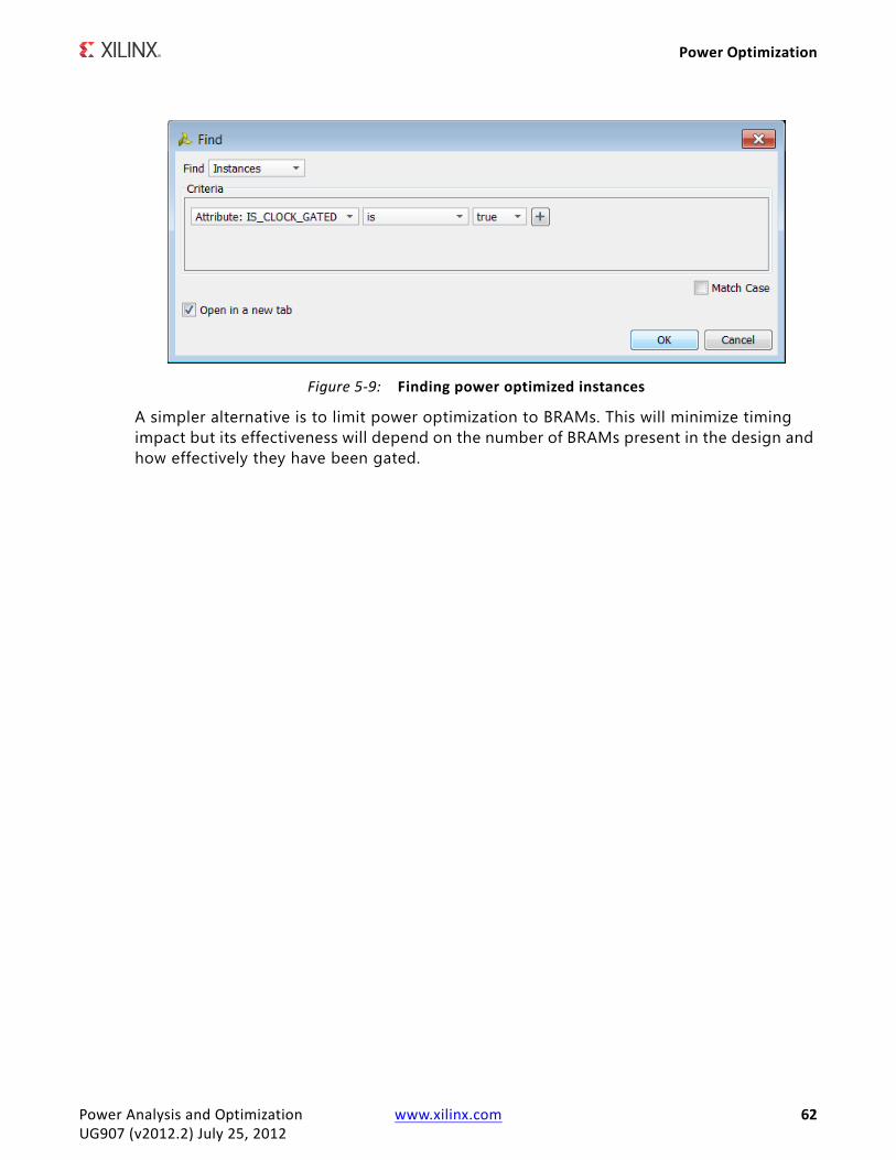
Power Optimization
A simpler alternative is to limit power optimization to BRAMs. This will minimize timing impact but its effectiveness will depend on the number of BRAMs present in the design and how effectively they have been gated.
X-Ref Target - Figure 5-9
Figure 5-9: Finding power optimized instances
Power Analysis and Optimization www.xilinx.com 62UG907 (v2012.2) July 25, 2012

Chapter 6
Tips and Techniques for Power Reduction
IntroductionThis chapter describes power reduction techniques and their expected effect on total device power. This information will help you evaluate your best options depending on your time, power budget, available resources, and freedom to change your design.
System LevelCooling StrategyCooling strategy ensures that heat generated from the device is extracted and absorbed by the environment. These cooling strategies, which are generally available at the beginning of the design and become less feasible in the later stages, have a significant impact on the device static power:
• Increase the airflow.
• Lower the ambient temperature.
• Use a heat sink (or a larger heat sink), or select a different regulator.
Supply StrategyVoltage has a large effect on both static and dynamic power. Active control of the voltage level ensures the desired voltage is applied to the device.
• Use switching regulators.
Switching regulators are more power eff icient than linear regulators, at the expense of requiring a higher component count.
• Use adjustable regulators.
Sense voltage as close as possible to the FPGA and to the highest consuming device if the same supply powers multiple FPGAs.
• Select regulators with tight tolerances.
Power Analysis and Optimization www.xilinx.com 63UG907 (v2012.2) July 25, 2012

System Level
Device Selection• Select the best device for the product.
Increasingly, power is becoming one of the primary factors for selecting a device. Select the device that best meets your density, functionality, and performance requirements and will also meet your power budget.
• Minimize the number of devices.
This saves space, I/O interconnect power, total leakage, and other factors. Typically, replacing multiple components (for example, processor and FPGA) with a single larger FPGA consumes less static power.
• Select the smallest device possible.
This reduces leakage. Typically in an FPGA family the same package may be available with different die sizes. You can, for instance, use a larger die during the prototyping and pre-series phase, then move to a smaller die for volume production.
• Select the largest package possible.
This increases heat dissipation. A larger package has a larger area to dissipate the die heat into the environment. A larger heat sink can be attached to the package upper side and more heat can escape onto the PCB via the bottom ball grid array.
• Use low voltage devices.
Some device families are available with a lower power option. The lower core voltage requirements translate into significant static and dynamic power savings.
• Use low leakage devices.
Some device families are available with a lower leakage or static power options in the form of specif ic speed or temperature grades. These devices may cost a bit more to purchase but you or the end user may be able to more than offset this with savings on the electricity bill or cooling hardware and system maintenance.
Power Analysis and Optimization www.xilinx.com 64UG907 (v2012.2) July 25, 2012

Design Level
Design LevelThe following sections describe tips and techniques that can be applied to the design to meet your design’s power budget.
Your design cycle will include a power closure phase under two main circumstances:
• You want to further optimize your design after constraints are met.
OR
• Your design has exceeded its power budget.
Further Optimizing The Design After it Meets Constraints Typically at this stage in the development process you want to minimize changes to the RTL, board power supply, and cooling parameters, since this involves a lot of verif ication or PCB respin costs. However, you can experiment with different software options and constraints to optimize your logic and routing resource counts, configuration, and activity. This minimizes dynamic power and reduces static power at the same time. Depending on your design margins a 15% to 20% savings for your core dynamic power is a reasonable expectation, with some designs showing even more power reduction.
My Power Budget is Exceeded! What Can I Do?Typically at this stage the pressure to get the system to market is getting high and many parameters in your system are well defined, such as the board environment and cooling options. Even though this restricts the type of engineering rework you can do, the following methodology should help identify and focus on the highest potential areas for power reduction.
Step 1: Which Power Budget is Exceeded?
GUI users can review the Summary view in the Vivado™ Power Analysis report, and command line users can use the Summary section of the report f ile. The On-Chip and Supply Power tables provide a high-level view of the power distribution. Navigate the Summary view to determine the type and amount of power that exceeds your budget.
Step 2: Identify the Area on Which to Focus
Review the different detailed views in the Vivado Power Analysis report or XPower Estimator. Analyze the environment parameters and the power distribution across the different resources used, the design hierarchy, and clock domains. When you f ind an area of the design where power seems high, the information following should help you determine the likely contributing factors.
Power Analysis and Optimization www.xilinx.com 65UG907 (v2012.2) July 25, 2012
Design Level
Step 3: Experiment
With the list of candidate areas in your design for power optimizations derived from the previous step, you can now sort this list from easiest to most involved and decide which optimization or experiment to perform next. The power tools allow you to do What If? analysis so you can quickly enter design changes and estimate the power implications without having to actually edit any code or constraint or rerun the implementation tools.
Use Device Resources More Efficiently
• Block RAM
° The amount of power block RAM consumes is directly proportional to the amount of time it is enabled. To save power, the block RAM enable can be driven Low on clock cycles when the block RAM is not used in the design. Block RAM Enable Rate, along with Clock rate, is an important parameter that must be considered for power optimization.
° Use the NO_CHANGE mode in the TDP mode if the output latches remain unchanged during a write operation. This mode is the most power eff icient. This mode is not available in the SDP mode because it is identical in behavior to WRITE_FIRST mode.
• I/O
I/O interfaces have to drive long distances with potentially more parasitic effects, hence they typically represent a large portion of the device power requirements.
° VCCAUX
Use the lowest VCCAUX possible. This minimizes both the static and dynamic power for this voltage supply.
° Inputs
Limit usage of internally referenced input standards.
° IODELAY
Set the HIGH_PERFORMANCE_MODE attribute on the IDELAY2 to FALSE. When FALSE, this attribute increases the output jitter, but consumes less power.
° IBUF_LOW_PWR
Set the IBUF_LOW_PWR attribute to TRUE on bidirectional and input I/Os. Make sure the design performance allows for this setting.
Power Analysis and Optimization www.xilinx.com 66UG907 (v2012.2) July 25, 2012
Design Level
° I/O Configuration
Review the I/O standard, drive strength, and on-chip termination settings in the context of your performance needs and evaluate if you can use lower drive strength using tristatable DCI I/O standards (T_DCI), get by without terminations, or use external terminations.
° Outputs
- Use the lowest slew/drive/voltage level supported by the receiving chip(s).
- No termination or series termination are preferred over parallel terminations. Signal integrity simulation tools can help with this determination.
- Consider whether using on-chip or off-chip termination is the best option given your device thermal budget, system cost, and board real estate requirements.
- Evaluate using lower voltage swing differential standards.
- Evaluate if your application allows you to use transceivers instead of large parallel busses.
- Evaluate the requirements of I/O features such as IBUF, IO DELAY, and others, and disable when performance allows.
• Transceivers
° The GTX/GTH/GTP transceiver supports a range of power-down modes that may save power if applicable.
° There are two types of adaptive filtering available to the GTX/GTH receiver depending on system level trade-offs between power and performance. Optimized for power with lower channel loss, the GTX/GTH/GTP receiver has a power-eff icient adaptive mode named the low-power mode (LPM).
° Each GTX/GTH/GTP transceiver provides support for generating the out-of-band (OOB) sequences described in the Serial ATA (SATA), Serial Attach SCSI (SAS) specification, and beaconing described in the PCI Express specif ication. If OOB sequence is not used, this could further save power.
° Pack the maximum number of transceivers into a single tile to minimize duplicating supporting circuits.
• Logic
You can optimize the design description using these methods:
° Minimize asynchronous control signals which prevent logic optimization and use more routing resources.
° Minimize the number of control sets. A control set consists of the unique grouping of a clock, clock enable, set, reset, and, in the case of LUT RAM, write enable signals. Control set information is important because count limits or sharing of signals
Power Analysis and Optimization www.xilinx.com 67UG907 (v2012.2) July 25, 2012
Design Level
within a slice may occur. This varies with the FPGA architecture, and when the limit is reached can prevent proximity packing of related logic, which would increase routing resources.
° Add pipeline levels to minimize the size of combinatorial logic cones. This minimizes the propagation of glitches between registers until signals reach their f inal state at each clock cycle.
° Use resource time sharing. These techniques minimize device resource usage by time multiplexing different functions to the same hardware resources. This allows you to use a smaller device or can reduce placement and routing congestion, which will lower both static and dynamic core power.
° Processes which are slow and similar can be performed on the same resources instead of separate resources. This requires careful thinking for how to buffer, multiplex, initialize, and control the data to be processed. Typical applications for such optimization are similar parallel processes, such as processing multiple input sensors. Instead of having as many processing units as inputs, you could use a single processing unit and make it run faster, so it processes input channels one after the other while ensuring the same response time for each output. An XPower Estimator What If? estimation can help you decide whether the power savings are worth the engineering effort.
° Use the DSP and BlockRAM optional registers. For example, in DSP blocks the multiplier or MREG registers, when enabled, are the most power eff icient implementation as they minimize the propagation of internal glitches between clock cycles.
Experiment Using the Vivado Power Optimizer Feature
To maximize power savings when you run the power optimizer in the Vivado tools, you should run power optimization on the entire design and not exclude portions of the design. If you do not see anticipated power savings after enabling power optimization, the three areas of potential debug are the global set and reset signals, block RAM enable generation and register clock gating. A low number of power optimization generated enables in this area could indicate the need to review coding practices or options/attributes set for design synthesis and implementation.
IMPORTANT: In the Vivado tools, power optimization works to minimize the impact on timing while maximizing power savings. However, in certain cases, timing may degrade after power optimization. For techniques to offset this impact, see Preserving Timing After Power Optimization in Chapter 5.
• Global set and reset signals
Where possible, minimize the use of asynchronous set/reset signals especially to datapath or pipeline flip-flops as well as block RAMs (BRAMs).
You should also consider constraining the global set and reset signals as dont_touch during the power_opt_design step to avoid their use as enables. Note that setting the
Power Analysis and Optimization www.xilinx.com 68UG907 (v2012.2) July 25, 2012
Design Level
dont_touch attribute in HDL will cause every step in the flow to obey this property. It is recommended that this option is set up as an XDC constraint only for the power optimization step. Here is an example of how to do this:
set_property DONT_TOUCH true [get_cells u1]
Finally, ensure that the signal rate and probabilities of the global set and reset signals are set correctly prior to running power optimizer and vectorless power estimation.
• Slice registers and SRLs
A number of different reasons could explain why power_opt_design might not be able to generate clock enables for slice registers or SRLs in the design. Some examples are:
° Having combinational loops in the design
° Using set/reset signals at the flip-flops and SRLs that are sourced from primary inputs to the design
° Using asynchronous set/reset signals at the datapath flip-flops
° Large number of clock domains in the design preventing enables being generated due to clock domain crossing issues
° SRL sizes: Typically the larger the number of shift register stages in the SRLs, the more diff icult it is to generate a single clock enable for all stages
• Block RAMs
Block RAM (BRAM) rich designs are excellent candidates for power savings. Vivado uses a variety of optimization techniques to generate enables and save power. If BRAM gating coverage is low after using power_opt_design, some of the possible reasons could be:
° BRAMs are mainly FIFO18E1/FIFO36E1 instances. These cannot be optimized by the tool.
° Memories inferred or instantiated are mainly in true dual port (TDP) mode using asynchronous clocks on their A and B ports that cannot be optimized by power_opt_design.
° Use of asynchronous reset signals to either the BRAMs themselves or to the address/write-enable flip-flops feeding the BRAMs.
Power Analysis and Optimization www.xilinx.com 69UG907 (v2012.2) July 25, 2012
Design Level
Experiment Within the Vivado Power Analysis Feature
In the Vivado Report Power dialog box you can make adjustments then rerun the analysis to review the power implications for these factors:
° Environment: Includes thermal parameters, process, or voltages.
° Design Activity: Adjust the activity of nets or instances in the design. Change one item or change multiple items at a time. You can also change:
- Clock domains: Adjust the switching frequency.
- Glue logic: Adjust the dynamic activity rate.
- I/Os: Adjust both static and dynamic activity probabilities. You can also adjust parameters for the external components connected to the device outputs, such as the load capacitance or the near-end board termination details.
- Signals: Adjust the dynamic activity rate for data signals. For control signals you can also adjust the static probability to evaluate power under different Clock Enable, Set, or Reset scenarios.
- Specif ic blocks: In addition to the dynamic activity probability you can also adjust the activity of control ports such as port enables or write enables on block RAMs.
Experiment Within XPower Estimator (XPE)
In XPE you can import the Vivado power analysis results from modules developed by multiple sources to review the total power once these separate IP blocks are implemented in the device. You can also evaluate situations where you would have to change the netlist, and evaluate the power implications, without having to actually make the code changes. For your design core logic XPE works at a coarser resolution then the Vivado power analysis, since you cannot adjust each logic element or signal individually in XPE.
In XPE, you can also experiment with:
° Resource usage
Explore reducing the resource count. Try remapping pieces of logic from slice logic to dedicated blocks such as BRAM or DSP, and vice versa.
° Resource configuration
Explore using different configuration settings for the design I/Os, block RAMs, clock generators, and other resources.
Power Analysis and Optimization www.xilinx.com 70UG907 (v2012.2) July 25, 2012
Design Level
Experiment Within RTL Code
If you need to modify your RTL code to reduce power you can experiment with adding a pipeline or performing power retiming around high-activity logic such as carry chains and XOR functions. Although long paths with carry chains tend to be on slower clock domains, they exhibit more glitching activity, which increases the design power. Retiming or pipelining these paths is often beneficial.
Step 4: Implement the Changes and Review the Power Saving
Once you have determined the best changes to make given your time, performance, and resource constraints, proceed with implementing them. It is worth mentioning that trying too many options or changes at once may not yield the best results because of potential conflicts or interactions between them. Best practice, if time allows, is to experiment with a few options at a time so you can evaluate their effect on power and other constraints before adding on other changes.
Power Analysis and Optimization www.xilinx.com 71UG907 (v2012.2) July 25, 2012

Power Analysis and Optimization www.xilinx.com 72UG907 (v2012.2) July 25, 2012
Appendix A
Additional Resources
Xilinx ResourcesFor support resources such as Answers, Documentation, Downloads, and Forums, see the Xilinx® Support website at:
www.xilinx.com/support.
For a glossary of technical terms used in Xilinx documentation, see:
www.xilinx.com/company/terms.htm.
Solution CentersSee the Xilinx Solution Centers for support on devices, software tools, and intellectual property at all stages of the design cycle. Topics include design assistance, advisories, and troubleshooting tips.
References• Vivado™ Design Suite 2012.2 Documentation
(http://www.xilinx.com/support/documentation/dt_vivado_vivado2012-2.htm)
• XPower Estimator User Guide (UG440)