Embed Size (px)
Citation preview
© Copyright 2012 Xilinx
Vivado Design Suite
Properties Reference Guide
UG912 (v2012.2) September 4, 2012
© Copyright 2012 Xilinx
Properties Reference Guide UG912 (v2012.2) September 4, 2012 www.xilinx.com 2
Notice of Disclaimer
The information disclosed to you hereunder (the "Materials") is provided solely for the selection and use of Xilinx products. To the
maximum extent permitted by applicable law: (1) Materials are made available "AS IS" and with all faults, Xilinx hereby DISCLAIMS
ALL WARRANTIES AND CONDITIONS, EXPRESS, IMPLIED, OR STATUTORY, INCLUDING BUT NOT LIMITED TO WARRANTIES OF
MERCHANTABILITY, NON-INFRINGEMENT, OR FITNESS FOR ANY PARTICULAR PURPOSE; and (2) Xilinx shall not be liable (whether
in contract or tort, including negligence, or under any other theory of liability) for any loss or damage of any kind or nature related
to, arising under, or in connection with, the Materials (including your use of the Materials), including for any direct, indirect, special,
incidental, or consequential loss or damage (including loss of data, profits, goodwill, or any type of loss or damage suffered as a
result of any action brought by a third party) even if such damage or loss was reasonably foreseeable or Xilinx had been advised of
the possibility of the same. Xilinx assumes no obligation to correct any errors contained in the Materials or to notify you of updates
to the Materials or to product specifications. You may not reproduce, modify, distribute, or publicly display the Materials without
prior written consent. Certain products are subject to the terms and conditions of the Limited Warranties which can be viewed at
http://www.xilinx.com/warranty.htm; IP cores can be subject to warranty and support terms contained in a license issued to you by
Xilinx. Xilinx products are not designed or intended to be fail-safe or for use in any application requiring fail-safe performance; you
assume sole risk and liability for use of Xilinx products in Critical Applications: http://www.xilinx.com/warranty.htm#critapps.
©Copyright 2012 Xilinx, Inc. Xilinx, the Xilinx logo, Artix, ISE, Kintex, Spartan, Virtex, Vivado, Zynq, and other designated brands
included herein are trademarks of Xilinx in the United States and other countries. All other trademarks are the property of their
respective owners.
Revision History
The following table shows the revision history for this document.
Date Version Revision
09/04/12 2012.2 Initial Xilinx release.
© Copyright 2012 Xilinx
Properties Reference Guide UG912 (v2012.2) September 4, 2012 www.xilinx.com 3
Table of Contents
Introduction .................................................................................................................................... 5
About This Guide ................................................................................................................................................... 5
Copying Syntax and Coding Examples from PDF Documents .............................................................. 5
Vivado Design Suite Properties ....................................................................................................... 6
Properties Information ......................................................................................................................................... 6
Properties Included ............................................................................................................................................... 6
ASYNC_REG .............................................................................................................................................................. 8
BEL ............................................................................................................................................................................. 10
CLOCK_DEDICATED_ROUTE ............................................................................................................................. 12
COMPATIBLE_CONFIG_MODES ...................................................................................................................... 14
DCI_CASCADE ........................................................................................................................................................ 16
DIFF_TERM .............................................................................................................................................................. 18
DONT_TOUCH ....................................................................................................................................................... 21
DRIVE ........................................................................................................................................................................ 23
HIODELAY_GROUP .............................................................................................................................................. 27
HLUTNM .................................................................................................................................................................. 30
IN_TERM .................................................................................................................................................................. 34
INTERNAL_VREF .................................................................................................................................................... 36
IOB ............................................................................................................................................................................. 38
IODELAY_GROUP .................................................................................................................................................. 40
IOSTANDARD ........................................................................................................................................................ 43
KEEP_HIERARCHY ................................................................................................................................................. 47
LOC ............................................................................................................................................................................ 49
LUTNM ..................................................................................................................................................................... 51
MARK_DEBUG........................................................................................................................................................ 55
PACKAGE_PIN ........................................................................................................................................................ 57
© Copyright 2012 Xilinx
Properties Reference Guide UG912 (v2012.2) September 4, 2012 www.xilinx.com 4
PROHIBIT ................................................................................................................................................................. 59
SLEW ......................................................................................................................................................................... 60
VCCAUX_IO ............................................................................................................................................................ 63
Additional Resources .................................................................................................................... 65
Xilinx Resources .................................................................................................................................................... 65
Solution Centers ................................................................................................................................................... 65
References .............................................................................................................................................................. 65
© Copyright 2012 Xilinx
Properties Reference Guide UG912 (v2012.2) September 4, 2012 www.xilinx.com 5
Chapter 1
Introduction
About This Guide
This Guide discusses the properties available for the Xilinx® Vivado™ Design Suite. It
consists of the following:
Chapter 1, this Introduction.
Chapter 2, Vivado Design Suite Properties, which contains a list of the Vivado
properties, including, for each property, a description, supported architectures,
applicable elements, values, syntax examples (Verilog, VHDL, and XDC), and affected
steps in the design.
Appendix A, Additional Resources, which contains references to other helpful
resources and documents available on the Xilinx Support Website.
Copying Syntax and Coding Examples from PDF Documents
This guide gives numerous syntax and coding examples to assist you in inserting
properties into your code. Problems may arise if you copy those examples directly from
the PDF document into your code.
PDF documents insert end of line markers into examples that wrap from line to line.
These markers cause errors in your code.
Copying examples that span more than one page carries extraneous header and
footer information along with the example. This information causes errors in your
code.
To avoid these problems, edit the example in an ASCII text editor to remove any
unnecessary markers or information, then paste it into your code.
Note You may skip this process for short examples that do not wrap from line to line.
© Copyright 2012 Xilinx
Properties Reference Guide UG912 (v2012.2) September 4, 2012 www.xilinx.com 6
Chapter 2
Vivado Design Suite Properties
Properties Information
This chapter provides information about Xilinx® Vivado™ Design Suite properties. Each
property contains, where applicable:
A description of the property, including its primary uses.
A list of the architectures which that property supports.
The applicable elements for the property.
The values that can be used with the property.
Syntax examples, including examples for Verilog, VHDL, and XDC.
A list of the affected steps in the design for the property.
Cross references to other related properties.
Properties Included
The properties discussed in this guide include:
ASYNC_REG
BEL
CLOCK_DEDICATED_ROUTE
COMPATIBLE_CONFIG_MODES
DCI_CASCADE
DIFF_TERM
DONT_TOUCH
DRIVE
HIODELAY_GROUP
HLUTNM
Properties Included
© Copyright 2012 Xilinx
Properties Reference Guide UG912 (v2012.2) September 4, 2012 www.xilinx.com 7
IN_TERM
INTERNAL_VREF
IOB
IODELAY_GROUP
IOSTANDARD
KEEP_HIERARCHY
LOC
LUTNM
MARK_DEBUG
PACKAGE_PIN
PROHIBIT
SLEW
VCCAUX_IO
Chapter 2: Vivado Design Suite Properties
© Copyright 2012 Xilinx
Properties Reference Guide UG912 (v2012.2) September 4, 2012 www.xilinx.com 8
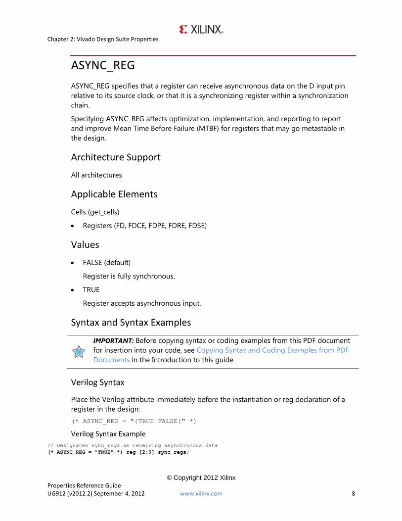
ASYNC_REG
ASYNC_REG specifies that a register can receive asynchronous data on the D input pin
relative to its source clock, or that it is a synchronizing register within a synchronization
chain.
Specifying ASYNC_REG affects optimization, implementation, and reporting to report
and improve Mean Time Before Failure (MTBF) for registers that may go metastable in
the design.
Architecture Support
All architectures
Applicable Elements
Cells (get_cells)
Registers (FD, FDCE, FDPE, FDRE, FDSE)
Values
FALSE (default)
Register is fully synchronous.
TRUE
Register accepts asynchronous input.
Syntax and Syntax Examples
IMPORTANT: Before copying syntax or coding examples from this PDF document
for insertion into your code, see Copying Syntax and Coding Examples from PDF
Documents in the Introduction to this guide.
Verilog Syntax
Place the Verilog attribute immediately before the instantiation or reg declaration of a
register in the design:
(* ASYNC_REG = "{TRUE|FALSE}" *)
Verilog Syntax Example
// Designates sync_regs as receiving asynchronous data
(* ASYNC_REG = "TRUE" *) reg [2:0] sync_regs;
ASYNC_REG
© Copyright 2012 Xilinx
Properties Reference Guide UG912 (v2012.2) September 4, 2012 www.xilinx.com 9
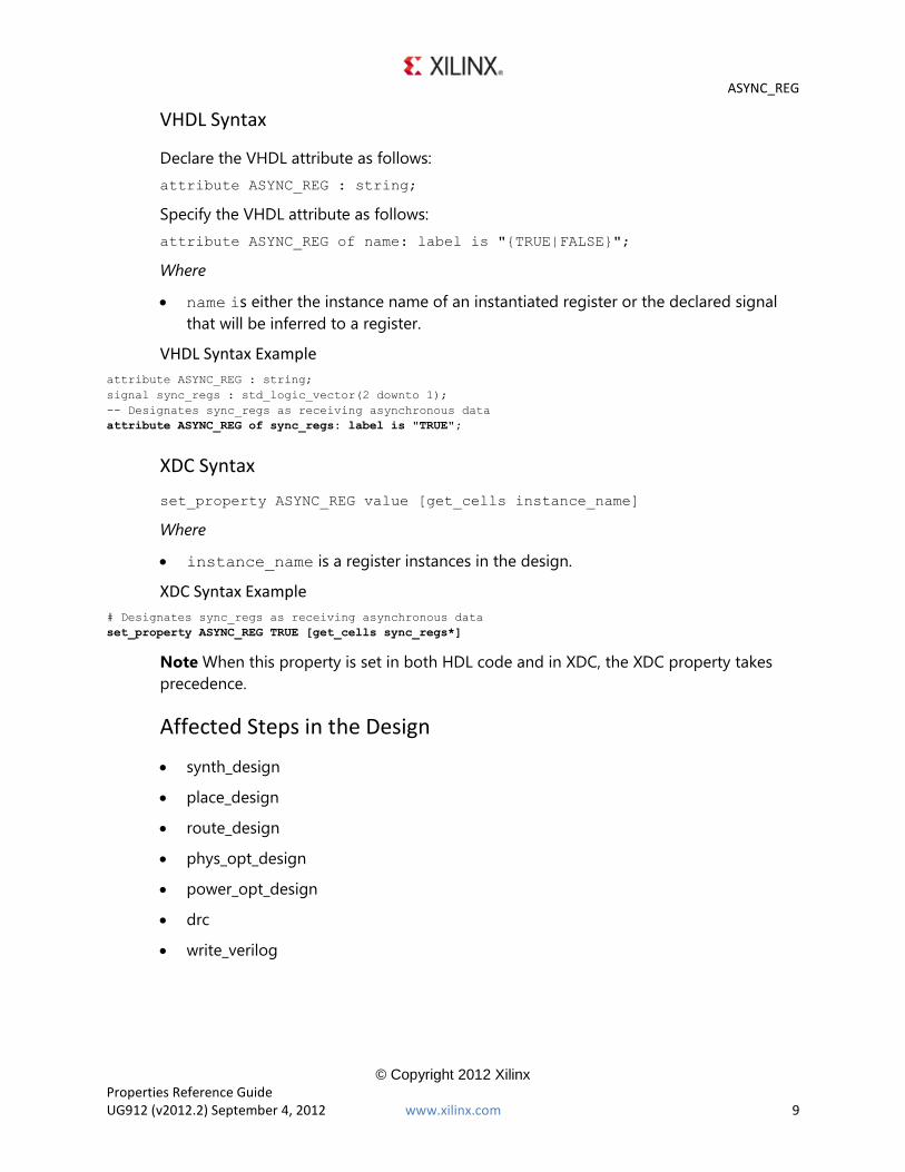
VHDL Syntax
Declare the VHDL attribute as follows:
attribute ASYNC_REG : string;
Specify the VHDL attribute as follows:
attribute ASYNC_REG of name: label is "{TRUE|FALSE}";
Where
name is either the instance name of an instantiated register or the declared signal
that will be inferred to a register.
VHDL Syntax Example
attribute ASYNC_REG : string;
signal sync_regs : std_logic_vector(2 downto 1);
-- Designates sync_regs as receiving asynchronous data
attribute ASYNC_REG of sync_regs: label is "TRUE";
XDC Syntax
set_property ASYNC_REG value [get_cells instance_name]
Where
instance_name is a register instances in the design.
XDC Syntax Example
# Designates sync_regs as receiving asynchronous data
set_property ASYNC_REG TRUE [get_cells sync_regs*]
Note When this property is set in both HDL code and in XDC, the XDC property takes
precedence.
Affected Steps in the Design
synth_design
place_design
route_design
phys_opt_design
power_opt_design
drc
write_verilog
Chapter 2: Vivado Design Suite Properties
© Copyright 2012 Xilinx
Properties Reference Guide UG912 (v2012.2) September 4, 2012 www.xilinx.com 10
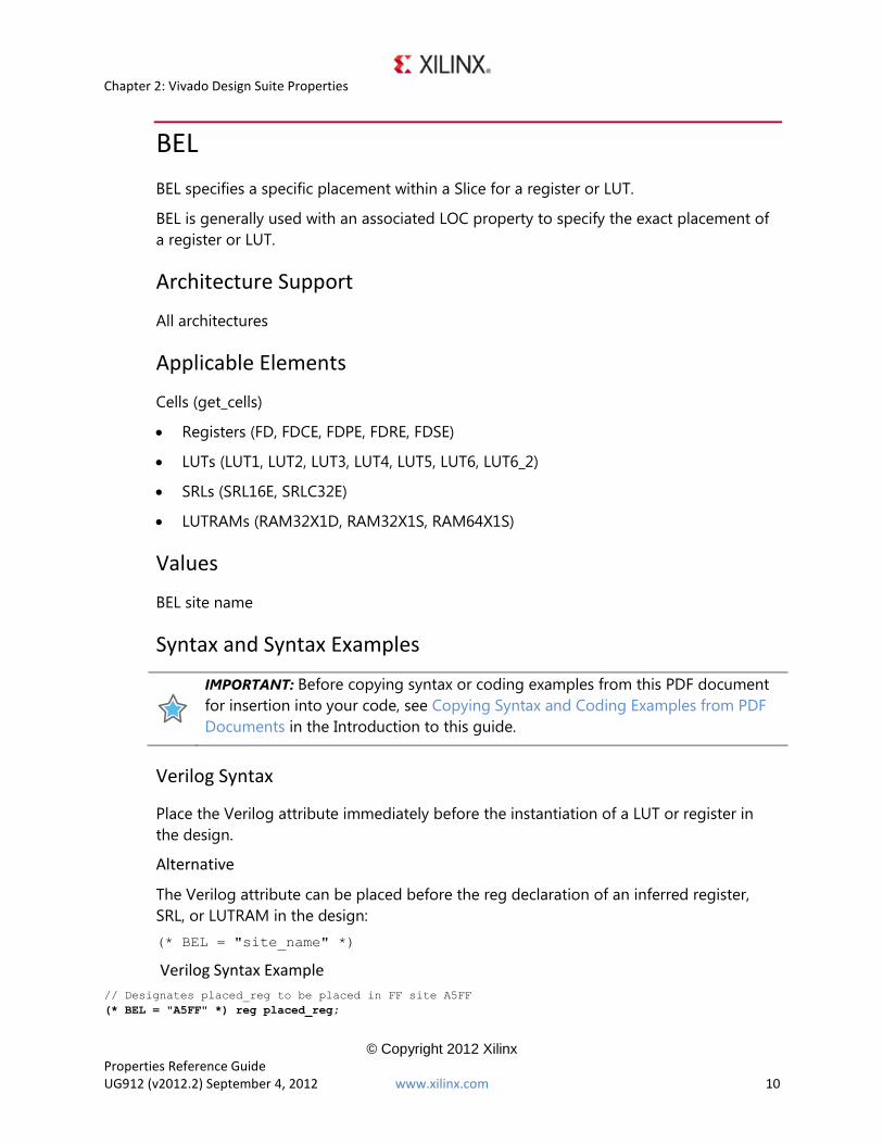
BEL
BEL specifies a specific placement within a Slice for a register or LUT.
BEL is generally used with an associated LOC property to specify the exact placement of
a register or LUT.
Architecture Support
All architectures
Applicable Elements
Cells (get_cells)
Registers (FD, FDCE, FDPE, FDRE, FDSE)
LUTs (LUT1, LUT2, LUT3, LUT4, LUT5, LUT6, LUT6_2)
SRLs (SRL16E, SRLC32E)
LUTRAMs (RAM32X1D, RAM32X1S, RAM64X1S)
Values
BEL site name
Syntax and Syntax Examples
IMPORTANT: Before copying syntax or coding examples from this PDF document
for insertion into your code, see Copying Syntax and Coding Examples from PDF
Documents in the Introduction to this guide.
Verilog Syntax
Place the Verilog attribute immediately before the instantiation of a LUT or register in
the design.
Alternative
The Verilog attribute can be placed before the reg declaration of an inferred register,
SRL, or LUTRAM in the design:
(* BEL = "site_name" *)
Verilog Syntax Example
// Designates placed_reg to be placed in FF site A5FF
(* BEL = "A5FF" *) reg placed_reg;
BEL
© Copyright 2012 Xilinx
Properties Reference Guide UG912 (v2012.2) September 4, 2012 www.xilinx.com 11
VHDL Syntax
Declare the VHDL attribute as follows:
attribute BEL : string;
For an instantiated instance, specify the VHDL attribute as follows:
attribute BEL of instance_name : label is "site_name";
Where
instance_name is the instance name of an instantiated register/LUT/SRL/LUTRAM.
VHDL Syntax Example
-- Designates instantiated register instance placed_reg to be placed in FF site A5FF
attribute BEL of placed_reg : label is "A5FF";
For an inferred instance, specify the VHDL attribute as follows:
attribute BEL of signal_name : signal is "site_name";
Where
signal_name is the signal name of an inferred register/LUT/SRL/LUTRAM.
VHDL Syntax Example
-- Designates instantiated register instance placed_reg to be placed in FF site A5FF
attribute BEL of placed_reg : signal is "A5FF";
XDC Syntax
set_property BEL site_name [get_cells instance_name]
Where
instance_name is a register, LUT, SRL, or LUTRAM instance in the design.
XDC Syntax Example
# Designates placed_reg to be placed in FF site A5FF
set_property BEL A5FF [get_cells placed_reg]
Note When this property is set in both HDL code and in XDC, the XDC property takes
precedence.
Affected Steps in the Design
Design Floorplanning
place_design
See Also
LOC
Chapter 2: Vivado Design Suite Properties
© Copyright 2012 Xilinx
Properties Reference Guide UG912 (v2012.2) September 4, 2012 www.xilinx.com 12
CLOCK_DEDICATED_ROUTE
CLOCK_DEDICATED_ROUTE provides a means to demote a clock placement DRC from an
error to a warning when a clock source is placed in a sub-optimal location compared to
its load clock buffer.
Setting CLOCK_DEDICATED_ROUTE to False may result in sub-optimal clock delays
resulting in potential timing and other issues.
Architecture Support
All architectures
Applicable Elements
Nets (get_nets)
Net connected to the input of a global clock buffer (BUFG, BUFGCE, BUFGMUX,
BUGCTRL)
Values
TRUE
FALSE
BACKBONE
Syntax and Syntax Examples
IMPORTANT: Before copying syntax or coding examples from this PDF document
for insertion into your code, see Copying Syntax and Coding Examples from PDF
Documents in the Introduction to this guide.
Verilog Syntax
Not applicable
VHDL Syntax
Not applicable
XDC Syntax
set_property CLOCK_DEDICATED_ROUTE value [get_nets net_name]
CLOCK_DEDICATED_ROUTE
© Copyright 2012 Xilinx
Properties Reference Guide UG912 (v2012.2) September 4, 2012 www.xilinx.com 13
Where
net_name is the signal name connected to the input of a global clock buffer.
XDC Syntax Example
# Designates clk_net to have relaxed clock placement rules
set_property CLOCK_DEDICATED_ROUTE FALSE [get_nets clk_net]
Affected Steps in the Design
place_design
DRC
Chapter 2: Vivado Design Suite Properties
© Copyright 2012 Xilinx
Properties Reference Guide UG912 (v2012.2) September 4, 2012 www.xilinx.com 14
COMPATIBLE_CONFIG_MODES
COMPATIBLE_CONFIG_MODES communicates which configuration mode to use for pin
allocations and proper DRC messaging.
Architecture Support
All architectures
Applicable Elements
Design (current_design)
Values
Slave Serial
Slave Serial Mode
Master Serial
Master Serial Mode
Slave SelectMap x8
Slave SelectMAP Mode, 8-bit width
Master SelectMap x8
Master SelectMAP Mode , 8-bit width
JTAG/Boundary Scan (default)
Boundary Scan Mode
Master SelectMap x16
Master SelectMAP Mode, 16-bit width
Slave SelectMap x32
Slave SelectMAP Mode, 32-bit width
Slave SelectMap x16
Slave SelectMAP Mode, 16-bit width
Master SPI x1
Serial Peripheral Interface, 1-bit width
Master SPI x2
Serial Peripheral Interface, 2-bit width
COMPATIBLE_CONFIG_MODES
© Copyright 2012 Xilinx
Properties Reference Guide UG912 (v2012.2) September 4, 2012 www.xilinx.com 15
Master SPI x4
Serial Peripheral Interface, 4-bit width
Master BPI-Up x8
Byte Peripheral Interface (Parallel NOR), 8-bit width
Master BPI-Up x16
Byte Peripheral Interface (Parallel NOR), 8-bit width
Syntax and Syntax Examples
IMPORTANT: Before copying syntax or coding examples from this PDF document
for insertion into your code, see Copying Syntax and Coding Examples from PDF
Documents in the Introduction to this guide.
Verilog Syntax
Not applicable
VHDL Syntax
Not applicable
XDC Syntax
set_property COMPATIBLE_CONFIG_MODES {value(s)} [current_design]
Note More than one configuration mode value can be supplied.
XDC Syntax Example
# Specify using Configuration Mode Serial Peripheral Interface, 4-bit width
set_property COMPATIBLE_CONFIG_MODES {{Master SPI x4}} [current_design]
Affected Steps in the Design
I/O Planning
place_design
DRC
Chapter 2: Vivado Design Suite Properties
© Copyright 2012 Xilinx
Properties Reference Guide UG912 (v2012.2) September 4, 2012 www.xilinx.com 16
DCI_CASCADE
DCI_CASCADE specifies which adjacent banks use the DCI Cascade feature, thereby
sharing reference resistors with a master bank.
DCI_CASCADE specifies which bank is the master bank and all associated slave banks for
this feature.
Architecture Support
Kintex™-7 devices
Virtex®-7 devices
Larger Zynq™ devices (XCZ030 and XC7Z045)
Applicable Elements
I/O Bank (get_iobanks)
High Performance (HP) bank type
Values
Valid High Performance (HP) bank numbers
Syntax and Syntax Examples
IMPORTANT: Before copying syntax or coding examples from this PDF document
for insertion into your code, see Copying Syntax and Coding Examples from PDF
Documents in the Introduction to this guide.
Verilog Syntax
Not applicable
VHDL Syntax
Not applicable
XDC Syntax
set_property DCI_CASCADE {slave_banks} [get_iobanks master_bank]
DCI_CASCADE
© Copyright 2012 Xilinx
Properties Reference Guide UG912 (v2012.2) September 4, 2012 www.xilinx.com 17
Where
slave_banks is a list of the bank numbers of the slave banks.
master_bank is the bank number of the designated master bank.
XDC Syntax Example
# Designate Bank 14 as a master DCI Cascade bank and Banks 15 and 16 as its slaves
set_property DCI_CASCADE {15 16} [get_iobanks 14]
Affected Steps in the Design
I/O planning
place_design
drc
write_bitstream
report_power
See Also
DCI_VALUE
Chapter 2: Vivado Design Suite Properties
© Copyright 2012 Xilinx
Properties Reference Guide UG912 (v2012.2) September 4, 2012 www.xilinx.com 18
DIFF_TERM
DIFF_TERM specifies differential termination use on differential input and bi-directional
buffers.
Architecture Support
All architectures
Applicable Elements
Ports (get_ports)
Input or bi-directional ports connected to a differential input buffer
Cells (get_cells)
Differential input or bi-directional buffer (all IBUFDS and IOBUFDS variants)
Values
FALSE (default)
Differential termination is disabled.
TRUE
Differential termination is enabled.
Syntax and Syntax Examples
IMPORTANT: Before copying syntax or coding examples from this PDF document
for insertion into your code, see Copying Syntax and Coding Examples from PDF
Documents in the Introduction to this guide.
Verilog Syntax
DIFF_TERM can be set within the design by assigning the DIFF_TERM parameter on the
instantiated differential buffer in the design.
RECOMMENDED: Use the instantiation template from the Language Templates or
the 7 Series Libraries Guide for HDL Designs (UG768) to specify the proper syntax.
DIFF_TERM
© Copyright 2012 Xilinx
Properties Reference Guide UG912 (v2012.2) September 4, 2012 www.xilinx.com 19
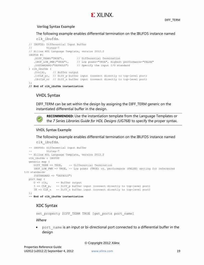
Verilog Syntax Example
The following example enables differential termination on the IBUFDS instance named
clk_ibufds.
// IBUFDS: Differential Input Buffer
// Virtex-7
// Xilinx HDL Language Template, version 2012.2
IBUFDS #(
.DIFF_TERM("TRUE"), // Differential Termination
.IBUF_LOW_PWR("TRUE"), // Low power="TRUE", Highest performance="FALSE"
.IOSTANDARD("DEFAULT") // Specify the input I/O standard
) clk_ibufds (
.O(clk), // Buffer output
.I(CLK_p), // Diff_p buffer input (connect directly to top-level port)
.IB(CLK_n) // Diff_n buffer input (connect directly to top-level port)
);
// End of clk_ibufds instantiation
VHDL Syntax
DIFF_TERM can be set within the design by assigning the DIFF_TERM generic on the
instantiated differential buffer in the design.
RECOMMENDED: Use the instantiation template from the Language Templates or
the 7 Series Libraries Guide for HDL Designs (UG768) to specify the proper syntax.
VHDL Syntax Example
The following example enables differential termination on the IBUFDS instance named
clk_ibufds.
-- IBUFDS: Differential Input Buffer
-- Virtex-7
-- Xilinx HDL Language Template, version 2012.2
clk_ibufds : IBUFDS
generic map (
DIFF_TERM => TRUE, -- Differential Termination
IBUF_LOW_PWR => TRUE, -- Low power (TRUE) vs. performance (FALSE) setting for referenced
I/O standards
IOSTANDARD => "DEFAULT")
port map (
O => clk, -- Buffer output
I => CLK_p, -- Diff_p buffer input (connect directly to top-level port)
IB => CLK_n -- Diff_n buffer input (connect directly to top-level port)
);
-- End of clk_ibufds instantiation
XDC Syntax
set_property DIFF_TERM TRUE [get_ports port_name]
Where
port_name is an input or bi-directional port connected to a differential buffer in the
design
Chapter 2: Vivado Design Suite Properties
© Copyright 2012 Xilinx
Properties Reference Guide UG912 (v2012.2) September 4, 2012 www.xilinx.com 20
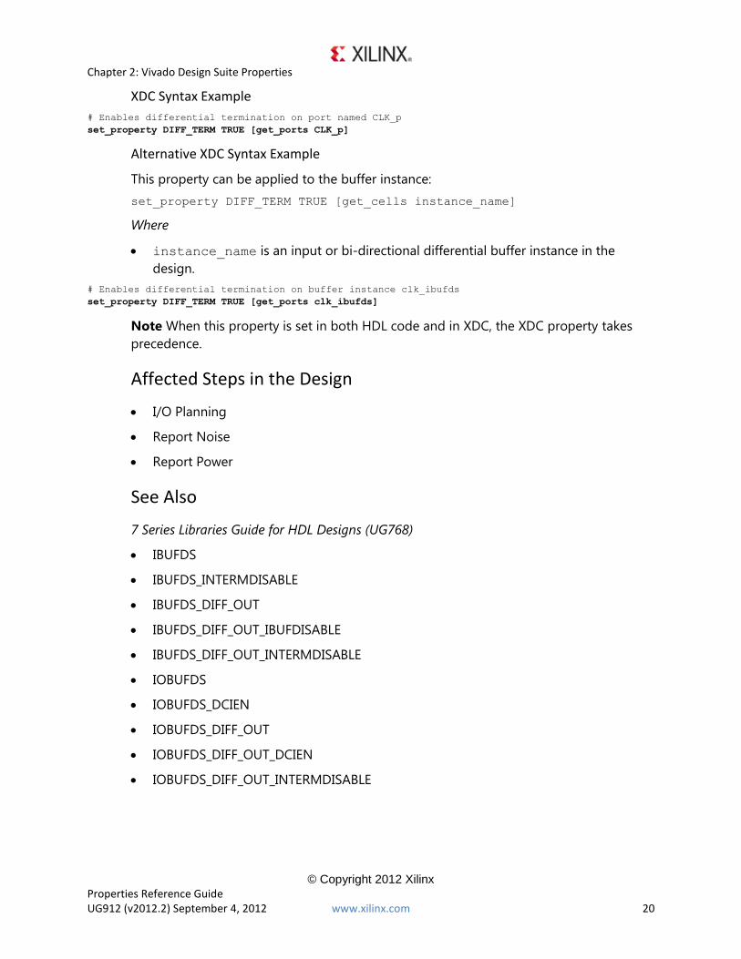
XDC Syntax Example
# Enables differential termination on port named CLK_p
set_property DIFF_TERM TRUE [get_ports CLK_p]
Alternative XDC Syntax Example
This property can be applied to the buffer instance:
set_property DIFF_TERM TRUE [get_cells instance_name]
Where
instance_name is an input or bi-directional differential buffer instance in the
design.
# Enables differential termination on buffer instance clk_ibufds
set_property DIFF_TERM TRUE [get_ports clk_ibufds]
Note When this property is set in both HDL code and in XDC, the XDC property takes
precedence.
Affected Steps in the Design
I/O Planning
Report Noise
Report Power
See Also
7 Series Libraries Guide for HDL Designs (UG768)
IBUFDS
IBUFDS_INTERMDISABLE
IBUFDS_DIFF_OUT
IBUFDS_DIFF_OUT_IBUFDISABLE
IBUFDS_DIFF_OUT_INTERMDISABLE
IOBUFDS
IOBUFDS_DCIEN
IOBUFDS_DIFF_OUT
IOBUFDS_DIFF_OUT_DCIEN
IOBUFDS_DIFF_OUT_INTERMDISABLE
DONT_TOUCH
© Copyright 2012 Xilinx
Properties Reference Guide UG912 (v2012.2) September 4, 2012 www.xilinx.com 21
DONT_TOUCH
DONT_TOUCH directs the tool to not optimize a user hierarchy or instantiated
component in the design so that optimization does not occur across its boundary. This
can be used to assist floorplanning, analysis, and debug efforts, but it may inhibit
optimization. This can result in a larger, slower design.
RECOMMENDED: Register all outputs of a module instance in which a
DONT_TOUCH is attached. To be most effective, apply this attribute before
synthesis.
Architecture Support
All architectures
Applicable Elements
Cells (get_cells)
User defined instance
Values
FALSE (default)
Allow optimization across hierarchy.
TRUE
Preserve hierarchy by not allowing any optimization across hierarchy boundary.
Syntax and Syntax Examples
IMPORTANT: Before copying syntax or coding examples from this PDF document
for insertion into your code, see Copying Syntax and Coding Examples from PDF
Documents in the Introduction to this guide.
Verilog Syntax
Place the Verilog attribute immediately before the user hierarchy instantiation in the
design:
(* DONT_TOUCH = "{TRUE|FALSE}" *)

Chapter 2: Vivado Design Suite Properties
© Copyright 2012 Xilinx
Properties Reference Guide UG912 (v2012.2) September 4, 2012 www.xilinx.com 22
Verilog Syntax Example
// Preserve the hierarchy of instance CLK1_rst_sync
(* DONT_TOUCH = "TRUE" *) reset_sync #(
.STAGES(5)
) CLK1_rst_sync (
.RST_IN(RST | ~LOCKED),
.CLK(clk1_100mhz),
.RST_OUT(rst_clk1)
);
VHDL Syntax
Declare the VHDL attribute as follows:
attribute DONT_TOUCH : string;
Specify the VHDL attribute as follows:
attribute DONT_TOUCH of name: label is "{TRUE|FALSE}";
Where
name is either the instance name of a user defined instance in the design.
VHDL Syntax Example
attribute DONT_TOUCH : string;
-- Preserve the hierarchy of instance CLK1_rst_sync
attribute DONT_TOUCH of CLK1_rst_sync: label is "TRUE";
…
CLK1_rst_sync : reset_sync
PORT MAP (
RST_IN => RST_LOCKED,
CLK => clk1_100mhz,
RST_OUT => rst_clk1
);
XDC Syntax
set_property DONT_TOUCH {TRUE|FALSE} [get_cells instance_name]
Where
instance_name is a register instances in the design.
XDC Syntax Example
# Preserve the hierarchy of instance CLK1_rst_sync
set_property DONT_TOUCH TRUE [get_cells CLK1_rst_sync]
Affected Steps in the Design
synth_design
opt_design
phys_opt_design
floorplanning
DRIVE
© Copyright 2012 Xilinx
Properties Reference Guide UG912 (v2012.2) September 4, 2012 www.xilinx.com 23
DRIVE
DRIVE specifies output buffer drive strength in mA for output buffers configured with I/O
standards that support programmable output drive strengths.
Architecture Support
All architectures
Applicable Elements
Ports (get_ports)
Output or bi-directional ports connected
Cells (get_cells)
Output Buffers (all OBUF variants)
Values
Integer values:
2
4
6
8
12 (default)
16
24
Syntax and Syntax Examples
IMPORTANT: Before copying syntax or coding examples from this PDF document
for insertion into your code, see Copying Syntax and Coding Examples from PDF
Documents in the Introduction to this guide.
Verilog Syntax
When inferring I/O buffers, the DRIVE attribute can be set in the design using the proper
Verilog attribute syntax placed before the top-level output port declaration:
(* DRIVE = "{2|4|6|8|12|16|24}" *)
Chapter 2: Vivado Design Suite Properties
© Copyright 2012 Xilinx
Properties Reference Guide UG912 (v2012.2) September 4, 2012 www.xilinx.com 24
Verilog Syntax Example
// Sets the drive strength on the STATUS output port to 2 mA
(* DRIVE = "2" *) output STATUS,
Alternative Verilog Syntax Example
If the output or bi-directional buffer is instantiated, DRIVE can be set within the design
by assigning the DRIVE parameter on the instantiated output buffer in the design.
RECOMMENDED: Use the instantiation template from the Language Templates or
the 7 Series Libraries Guide for HDL Designs (UG768) to specify the proper syntax.
The following example sets the drive strength on the OBUF instance named
status_obuf to 2 mA:
// OBUF: Single-ended Output Buffer
// Virtex-7
// Xilinx HDL Language Template, version 2012.2
OBUF #(
.DRIVE(2), // Specify the output drive strength
.IOSTANDARD("DEFAULT"), // Specify the output I/O standard
.SLEW("SLOW") // Specify the output slew rate
) status_obuf (
.O(STATUS), // Buffer output (connect directly to top-level port)
.I(status_int) // Buffer input
);
// End of status_obuf instantiation
VHDL Syntax
When inferring I/O buffers, the DRIVE attribute can be set in the design using the proper
VHDL attribute syntax placed before the top-level output port declaration.
Declare the VHDL attribute as follows:
attribute DRIVE : integer;
Specify the VHDL attribute as follows:
attribute DRIVE of port_name : signal is value;
Where
port_name is a top-level output port in the design.
VHDL Syntax Example
STATUS : out std_logic;
attribute DRIVE : integer;
-- Sets the drive strength on the STATUS output port to 2 mA
attribute DRIVE of STATUS : signal is 2;
Alternative VHDL Syntax Example
If the output or bi-directional buffer is instantiated, DRIVE can be set within the design
by assigning the DRIVE generic on the instantiated output buffer in the design.
DRIVE
© Copyright 2012 Xilinx
Properties Reference Guide UG912 (v2012.2) September 4, 2012 www.xilinx.com 25
RECOMMENDED: Use the instantiation template from the Language Templates or
the 7 Series Libraries Guide for HDL Designs (UG768) to specify the proper syntax.
The following example sets the drive strength on the OBUF instance named
status_obuf to 2 mA.
-- OBUF: Single-ended Output Buffer
-- Virtex-7
-- Xilinx HDL Language Template, version 2012.2
status_obuf : OBUF
generic map (
DRIVE => 2,
IOSTANDARD => "DEFAULT",
SLEW => "SLOW")
port map (
O => STATUS, -- Buffer output (connect directly to top-level port)
I => status_int -- Buffer input
);
-- End of status_obuf instantiation
XDC Syntax
set_property DRIVE value [get_ports port_name]
Where
port_name is an output or bi-directional port in the design
XDC Syntax Example
# Sets the drive strength of the port STATUS to 2 mA
set_property DRIVE 2 [get_ports STATUS]
Note When this property is set in both HDL code and in XDC, the XDC property takes
precedence.
Affected Steps in the Design
I/O Planning
Report Noise
Report Power
Chapter 2: Vivado Design Suite Properties
© Copyright 2012 Xilinx
Properties Reference Guide UG912 (v2012.2) September 4, 2012 www.xilinx.com 26
See Also
7 Series Libraries Guide for HDL Designs (UG768)
OBUF
OBUFT
IOBUF
IOBUF_DCIEN
IOBUF_INTERM_DISABLE
HIODELAY_GROUP
© Copyright 2012 Xilinx
Properties Reference Guide UG912 (v2012.2) September 4, 2012 www.xilinx.com 27
HIODELAY_GROUP
HIODELAY_GROUP groups IDELAYCTRL components to their associated IDELAY or
ODELAY instances for proper placement and replication.
Difference Between HIODELAY_GROUP and IODELAY_GROUP
HIODELAY_GROUP is uniquified per hierarchy.
Use HIODELAY_GROUP when:
You expect to have multiple instances of a module that contains an IDELAYCTRL.
and
That instance is not intended to be grouped with any IDELAY or ODELAY instances in
other logical hierarchies.
Architecture Support
All architectures
Applicable Elements
Cells (get_cells)
IDELAY, ODELAY, or IDELAYCTRL instances
Values
Any specified group name
Syntax and Syntax Examples
IMPORTANT: Before copying syntax or coding examples from this PDF document
for insertion into your code, see Copying Syntax and Coding Examples from PDF
Documents in the Introduction to this guide.
Verilog Syntax
Place the Verilog attribute immediately before the instantiation of an IDELAY, ODELAY, or
IDELAYCTRL in the design.
(* HIODELAY_GROUP = "value" *)
Chapter 2: Vivado Design Suite Properties
© Copyright 2012 Xilinx
Properties Reference Guide UG912 (v2012.2) September 4, 2012 www.xilinx.com 28
Verilog Syntax Example
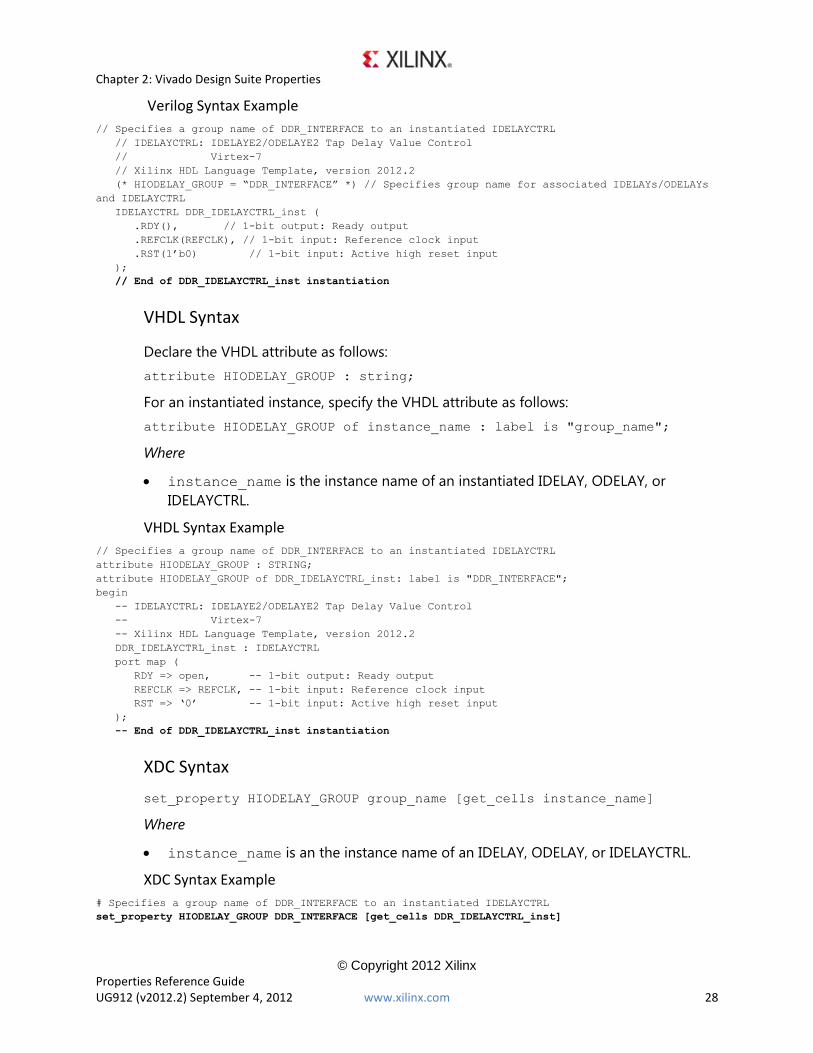
// Specifies a group name of DDR_INTERFACE to an instantiated IDELAYCTRL
// IDELAYCTRL: IDELAYE2/ODELAYE2 Tap Delay Value Control
// Virtex-7
// Xilinx HDL Language Template, version 2012.2
(* HIODELAY_GROUP = “DDR_INTERFACE” *) // Specifies group name for associated IDELAYs/ODELAYs
and IDELAYCTRL
IDELAYCTRL DDR_IDELAYCTRL_inst (
.RDY(), // 1-bit output: Ready output
.REFCLK(REFCLK), // 1-bit input: Reference clock input
.RST(1‟b0) // 1-bit input: Active high reset input
);
// End of DDR_IDELAYCTRL_inst instantiation
VHDL Syntax
Declare the VHDL attribute as follows:
attribute HIODELAY_GROUP : string;
For an instantiated instance, specify the VHDL attribute as follows:
attribute HIODELAY_GROUP of instance_name : label is "group_name";
Where
instance_name is the instance name of an instantiated IDELAY, ODELAY, or
IDELAYCTRL.
VHDL Syntax Example
// Specifies a group name of DDR_INTERFACE to an instantiated IDELAYCTRL
attribute HIODELAY_GROUP : STRING;
attribute HIODELAY_GROUP of DDR_IDELAYCTRL_inst: label is "DDR_INTERFACE";
begin
-- IDELAYCTRL: IDELAYE2/ODELAYE2 Tap Delay Value Control
-- Virtex-7
-- Xilinx HDL Language Template, version 2012.2
DDR_IDELAYCTRL_inst : IDELAYCTRL
port map (
RDY => open, -- 1-bit output: Ready output
REFCLK => REFCLK, -- 1-bit input: Reference clock input
RST => „0‟ -- 1-bit input: Active high reset input
);
-- End of DDR_IDELAYCTRL_inst instantiation
XDC Syntax
set_property HIODELAY_GROUP group_name [get_cells instance_name]
Where
instance_name is an the instance name of an IDELAY, ODELAY, or IDELAYCTRL.
XDC Syntax Example
# Specifies a group name of DDR_INTERFACE to an instantiated IDELAYCTRL
set_property HIODELAY_GROUP DDR_INTERFACE [get_cells DDR_IDELAYCTRL_inst]
HIODELAY_GROUP
© Copyright 2012 Xilinx
Properties Reference Guide UG912 (v2012.2) September 4, 2012 www.xilinx.com 29
Note When this property is set in both HDL code and in XDC, the XDC property takes
precedence.
Affected Steps in the Design
place_design
See Also
IODELAY_GROUP
7 Series Libraries Guide for HDL Designs (UG768)
IDELAYCTRL
IDELAYE2
ODELAYE2
Chapter 2: Vivado Design Suite Properties
© Copyright 2012 Xilinx
Properties Reference Guide UG912 (v2012.2) September 4, 2012 www.xilinx.com 30
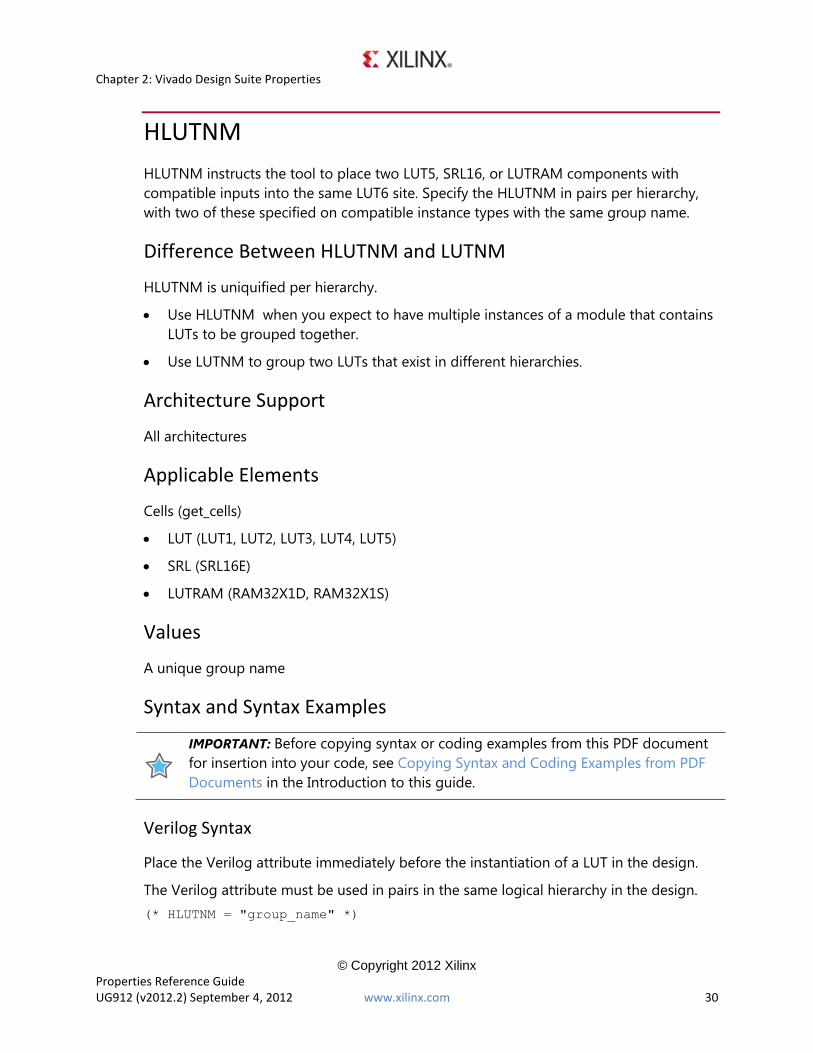
HLUTNM
HLUTNM instructs the tool to place two LUT5, SRL16, or LUTRAM components with
compatible inputs into the same LUT6 site. Specify the HLUTNM in pairs per hierarchy,
with two of these specified on compatible instance types with the same group name.
Difference Between HLUTNM and LUTNM
HLUTNM is uniquified per hierarchy.
Use HLUTNM when you expect to have multiple instances of a module that contains
LUTs to be grouped together.
Use LUTNM to group two LUTs that exist in different hierarchies.
Architecture Support
All architectures
Applicable Elements
Cells (get_cells)
LUT (LUT1, LUT2, LUT3, LUT4, LUT5)
SRL (SRL16E)
LUTRAM (RAM32X1D, RAM32X1S)
Values
A unique group name
Syntax and Syntax Examples
IMPORTANT: Before copying syntax or coding examples from this PDF document
for insertion into your code, see Copying Syntax and Coding Examples from PDF
Documents in the Introduction to this guide.
Verilog Syntax
Place the Verilog attribute immediately before the instantiation of a LUT in the design.
The Verilog attribute must be used in pairs in the same logical hierarchy in the design.
(* HLUTNM = "group_name" *)
HLUTNM
© Copyright 2012 Xilinx
Properties Reference Guide UG912 (v2012.2) September 4, 2012 www.xilinx.com 31
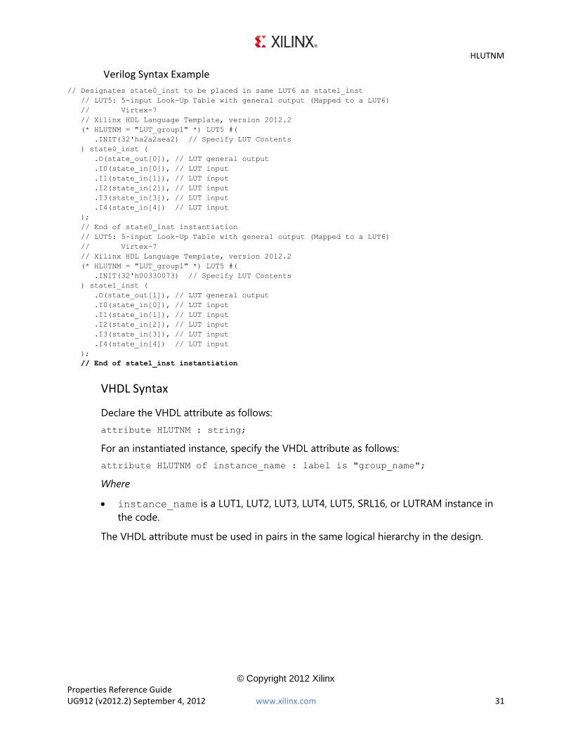
Verilog Syntax Example
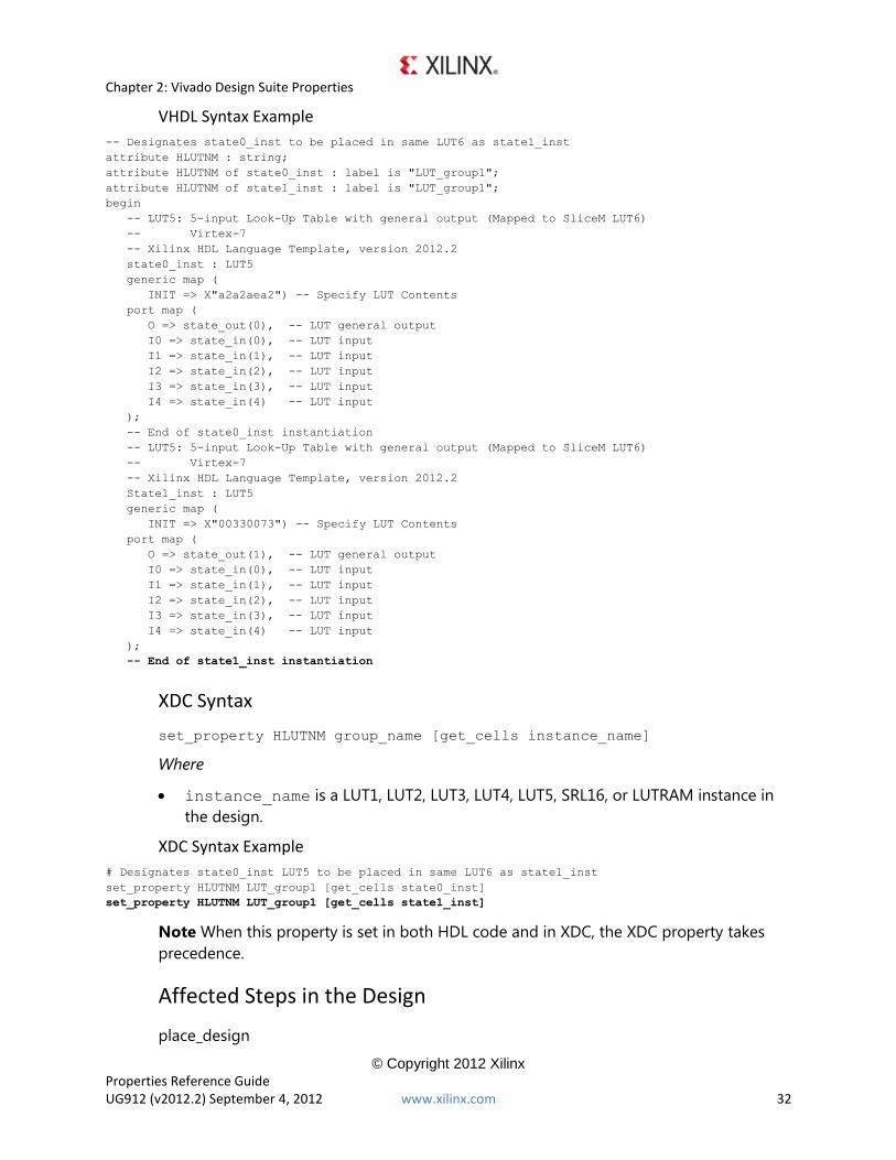
// Designates state0_inst to be placed in same LUT6 as state1_inst
// LUT5: 5-input Look-Up Table with general output (Mapped to a LUT6)
// Virtex-7
// Xilinx HDL Language Template, version 2012.2
(* HLUTNM = "LUT_group1" *) LUT5 #(
.INIT(32'ha2a2aea2) // Specify LUT Contents
) state0_inst (
.O(state_out[0]), // LUT general output
.I0(state_in[0]), // LUT input
.I1(state_in[1]), // LUT input
.I2(state_in[2]), // LUT input
.I3(state_in[3]), // LUT input
.I4(state_in[4]) // LUT input
);
// End of state0_inst instantiation
// LUT5: 5-input Look-Up Table with general output (Mapped to a LUT6)
// Virtex-7
// Xilinx HDL Language Template, version 2012.2
(* HLUTNM = "LUT_group1" *) LUT5 #(
.INIT(32'h00330073) // Specify LUT Contents
) state1_inst (
.O(state_out[1]), // LUT general output
.I0(state_in[0]), // LUT input
.I1(state_in[1]), // LUT input
.I2(state_in[2]), // LUT input
.I3(state_in[3]), // LUT input
.I4(state_in[4]) // LUT input
);
// End of state1_inst instantiation
VHDL Syntax
Declare the VHDL attribute as follows:
attribute HLUTNM : string;
For an instantiated instance, specify the VHDL attribute as follows:
attribute HLUTNM of instance_name : label is "group_name";
Where
instance_name is a LUT1, LUT2, LUT3, LUT4, LUT5, SRL16, or LUTRAM instance in
the code.
The VHDL attribute must be used in pairs in the same logical hierarchy in the design.
Chapter 2: Vivado Design Suite Properties
© Copyright 2012 Xilinx
Properties Reference Guide UG912 (v2012.2) September 4, 2012 www.xilinx.com 32
VHDL Syntax Example
-- Designates state0_inst to be placed in same LUT6 as state1_inst
attribute HLUTNM : string;
attribute HLUTNM of state0_inst : label is "LUT_group1";
attribute HLUTNM of state1_inst : label is "LUT_group1";
begin
-- LUT5: 5-input Look-Up Table with general output (Mapped to SliceM LUT6)
-- Virtex-7
-- Xilinx HDL Language Template, version 2012.2
state0_inst : LUT5
generic map (
INIT => X"a2a2aea2") -- Specify LUT Contents
port map (
O => state_out(0), -- LUT general output
I0 => state_in(0), -- LUT input
I1 => state_in(1), -- LUT input
I2 => state_in(2), -- LUT input
I3 => state_in(3), -- LUT input
I4 => state_in(4) -- LUT input
);
-- End of state0_inst instantiation
-- LUT5: 5-input Look-Up Table with general output (Mapped to SliceM LUT6)
-- Virtex-7
-- Xilinx HDL Language Template, version 2012.2
State1_inst : LUT5
generic map (
INIT => X"00330073") -- Specify LUT Contents
port map (
O => state_out(1), -- LUT general output
I0 => state_in(0), -- LUT input
I1 => state_in(1), -- LUT input
I2 => state_in(2), -- LUT input
I3 => state_in(3), -- LUT input
I4 => state_in(4) -- LUT input
);
-- End of state1_inst instantiation
XDC Syntax
set_property HLUTNM group_name [get_cells instance_name]
Where
instance_name is a LUT1, LUT2, LUT3, LUT4, LUT5, SRL16, or LUTRAM instance in
the design.
XDC Syntax Example
# Designates state0_inst LUT5 to be placed in same LUT6 as state1_inst
set_property HLUTNM LUT_group1 [get_cells state0_inst]
set_property HLUTNM LUT_group1 [get_cells state1_inst]
Note When this property is set in both HDL code and in XDC, the XDC property takes
precedence.
Affected Steps in the Design
place_design
HLUTNM
© Copyright 2012 Xilinx
Properties Reference Guide UG912 (v2012.2) September 4, 2012 www.xilinx.com 33
See Also
LUTNM
Chapter 2: Vivado Design Suite Properties
© Copyright 2012 Xilinx
Properties Reference Guide UG912 (v2012.2) September 4, 2012 www.xilinx.com 34
IN_TERM
IN_TERM specifies an uncalibrated input termination impedance value.
IN_TERM is supported on High Range (HR) bank inputs only.
Note For inputs in High Performance (HP) banks, use Digital Controlled Impedance (DCI)
circuits for on-chip termination.
Architecture Support
All architectures on High Range (HR) bank inputs only
Applicable Elements
Ports (get_ports)
Input or bi-directional ports connected
Cells (get_cells)
Input Buffers (all IBUF variants)
Values
NONE (default)
UNTUNED_SPLIT_25
UNTUNED_SPLIT_50
UNTINED_SPLIT_75
Syntax and Syntax Examples
IMPORTANT: Before copying syntax or coding examples from this PDF document
for insertion into your code, see Copying Syntax and Coding Examples from PDF
Documents in the Introduction to this guide.
Verilog Syntax
The IN_TERM attribute can be set in the design using the proper Verilog attribute syntax
placed before the top-level output port declaration:
(* IN_TERM = "{NONE|UNTUNED_SPLIT_25|UNTUNED_SPLIT_50|UNTUNED_SPLIT_75}" *)
Verilog Syntax Example
// Sets an on-chip input impedance of 50 Ohms to input ACT5
(* IN_TERM = "UNTUNED_SPLIT_50" *) input ACT5,
IN_TERM
© Copyright 2012 Xilinx
Properties Reference Guide UG912 (v2012.2) September 4, 2012 www.xilinx.com 35
VHDL Syntax
The IN_TERM attribute can be set in the design using the proper VHDL attribute syntax
placed before the top-level output port declaration.
Declare the VHDL attribute as follows:
attribute IN_TERM : string;
Specify the VHDL attribute as follows:
attribute IN_TERM of port_name : signal is value;
Where
port_name is a top-level output port in the design.
VHDL Syntax Example
ACT5 : in std_logic;
attribute IN_TERM : string;
-- Sets an on-chip input impedance of 50 Ohms to input ACT5
attribute IN_TERM of ACT5 : signal is “UNTUNED_SPLIT_50”;
XDC Syntax
set_property IN_TERM value [get_ports port_name]
Where
port_name is an output or bi-directional port in the design.
XDC Syntax Example
# Sets an on-chip input impedance of 50 Ohms to input ACT5
set_property IN_TERM UNTUNED_SPLIT_50 [get_ports ACT5]
Note When this property is set in both HDL code and in XDC, the XDC property takes
precedence.
Affected Steps in the Design
I/O Planning
Report Noise
Report Power
See Also
DCI_VALUE
Chapter 2: Vivado Design Suite Properties
© Copyright 2012 Xilinx
Properties Reference Guide UG912 (v2012.2) September 4, 2012 www.xilinx.com 36
INTERNAL_VREF
INTERNAL_VREF specifies the use of an internal regulator on a bank to supply the
voltage reference for standards requiring a reference voltage.
Architecture Support
All architectures
Applicable Elements
I/O Bank (get_iobanks)
Values
0.60
0.675
0.75
0.90
Syntax and Syntax Examples
IMPORTANT: Before copying syntax or coding examples from this PDF document
for insertion into your code, see Copying Syntax and Coding Examples from PDF
Documents in the Introduction to this guide.
Verilog Syntax
Not applicable
VHDL Syntax
Not applicable
XDC Syntax
set_property INTERNAL_VREF {value} [get_iobanks bank]
Where
value is the reference voltage value.
INTERNAL_VREF
© Copyright 2012 Xilinx
Properties Reference Guide UG912 (v2012.2) September 4, 2012 www.xilinx.com 37
XDC Syntax Example
# Designate Bank 14 to have a reference voltage of 0.75 Volts
set_property INTERNAL_VREF 0.75 [get_iobanks 14]
Affected Steps in the Design
I/O planning
place_design
drc
report_power
Chapter 2: Vivado Design Suite Properties
© Copyright 2012 Xilinx
Properties Reference Guide UG912 (v2012.2) September 4, 2012 www.xilinx.com 38
IOB
IOB directs the tool to place a register in the input or output logic to improve I/O timing.
Architecture Support
All architectures
Applicable Elements
Ports (get_ports)
Any port connected to a register
Cells (get_cells)
Registers connected directly to a top-level port
Values
TRUE
FALSE (default)
Syntax and Syntax Examples
IMPORTANT: Before copying syntax or coding examples from this PDF document
for insertion into your code, see Copying Syntax and Coding Examples from PDF
Documents in the Introduction to this guide.
Verilog Syntax
The IOB attribute can be set in the design using the proper Verilog attribute syntax
placed before the top-level output port declaration:
(* IOB = "{TRUE|FALSE}" *)
Verilog Syntax Example
// Place the register connected to ACK in the input logic site
(* IOB = "TRUE" *) input ACK,
Alternative Verilog Syntax Example
The IOB attribute can be placed on an instantiated or inferred register connected to a
top-level port.
IOB
© Copyright 2012 Xilinx
Properties Reference Guide UG912 (v2012.2) September 4, 2012 www.xilinx.com 39
Place the register connected to ACK in the input logic site.
input ACK;
(* IOB = “TRUE” *) reg ack_reg = 1‟b0;
always @(posedge CLK)
ack_reg = 1’b0;
VHDL Syntax
The IOB attribute can be set in the design using the proper VHDL attribute syntax placed
before the top-level output port declaration.
Declare the VHDL attribute as follows:
attribute IOB : string;
Specify the VHDL attribute as follows:
attribute IOB of <port_name>: signal is "{TRUE|FALSE}";
Where
port_name is a top-level output port in the design.
VHDL Syntax Example
ACK : in std_logic;
attribute IOB : string;
-- Place the register connected to ACK in the input logic site
attribute IOB of ACK: signal is "TRUE";
Alternative VHDL Syntax Example
The IOB attribute can be placed on an instantiated or inferred register connected to a
top-level port.
Place the register connected to ACK in the input logic site.
XDC Syntax
set_property IOB value [get_ports port_name]
Where
value is TRUE or FALSE.
XDC Syntax Example
# Place the register connected to ACK in the input logic site
set_property IOB TRUE [get_ports ACK]
Note When this property is set in both HDL code and in XDC, the XDC property takes
precedence.
Affected Steps in the Design
place_design
Chapter 2: Vivado Design Suite Properties
© Copyright 2012 Xilinx
Properties Reference Guide UG912 (v2012.2) September 4, 2012 www.xilinx.com 40
IODELAY_GROUP
IODELAY_GROUP Groups IDELAYCTRL components to their associated IDELAY and
ODELAY instances so that proper placement and replication may occur in the design.
Difference Between IODELAY_GROUP and HIODELAY_GROUP
IODELAY_GROUP can group elements in different hierarchies.
Use IODELAY_GROUP to group I/O delay components in different hierarchies together.
Architecture Support
All architectures
Applicable Elements
Cells (get_cells)
IDELAY, ODELAY, or IDELAYCTRL instances
Values
Any specified group name
Syntax and Syntax Examples
IMPORTANT: Before copying syntax or coding examples from this PDF document
for insertion into your code, see Copying Syntax and Coding Examples from PDF
Documents in the Introduction to this guide.
Verilog Syntax
Place the Verilog attribute immediately before the instantiation of an IDELAY, ODELAY, or
IDELAYCTRL in the design.
(* IODELAY_GROUP = "value" *)
IODELAY_GROUP
© Copyright 2012 Xilinx
Properties Reference Guide UG912 (v2012.2) September 4, 2012 www.xilinx.com 41
Verilog Syntax Example
// Specifies a group name of DDR_INTERFACE to an instantiated IDELAYCTRL
// IDELAYCTRL: IDELAYE2/ODELAYE2 Tap Delay Value Control
// Virtex-7
// Xilinx HDL Language Template, version 2012.2
(* IODELAY_GROUP = “DDR_INTERFACE” *) // Specifies group name for associated IDELAYs/ODELAYs
and IDELAYCTRL
IDELAYCTRL DDR_IDELAYCTRL_inst (
.RDY(), // 1-bit output: Ready output
.REFCLK(REFCLK), // 1-bit input: Reference clock input
.RST(1‟b0) // 1-bit input: Active high reset input
);
// End of DDR_IDELAYCTRL_inst instantiation
VHDL Syntax
Declare the VHDL attribute as follows:
attribute IODELAY_GROUP : string;
For an instantiated instance, specify the VHDL attribute as follows:
attribute IODELAY_GROUP of instance_name : label is "group_name";
Where
instance_name is the instance name of an instantiated IDELAY, ODELAY, or
IDELAYCTRL.
VHDL Syntax Example
// Specifies a group name of DDR_INTERFACE to an instantiated IDELAYCTRL
attribute IODELAY_GROUP : STRING;
attribute IODELAY_GROUP of DDR_IDELAYCTRL_inst: label is "DDR_INTERFACE";
begin
-- IDELAYCTRL: IDELAYE2/ODELAYE2 Tap Delay Value Control
-- Virtex-7
-- Xilinx HDL Language Template, version 2012.2
DDR_IDELAYCTRL_inst : IDELAYCTRL
port map (
RDY => open, -- 1-bit output: Ready output
REFCLK => REFCLK, -- 1-bit input: Reference clock input
RST => „0‟ -- 1-bit input: Active high reset input
);
-- End of DDR_IDELAYCTRL_inst instantiation
XDC Syntax
set_property IODELAY_GROUP group_name [get_cells instance_name]
Where
instance_name is an the instance name of an IDELAY, ODELAY, or IDELAYCTRL.
XDC Syntax Example
# Specifies a group name of DDR_INTERFACE to an instantiated IDELAYCTRL
set_property IODELAY_GROUP DDR_INTERFACE [get_cells DDR_IDELAYCTRL_inst]
Chapter 2: Vivado Design Suite Properties
© Copyright 2012 Xilinx
Properties Reference Guide UG912 (v2012.2) September 4, 2012 www.xilinx.com 42
Note When this property is set in both HDL code and in XDC, the XDC property takes
precedence.
Affected Steps in the Design
place_design
See Also
HIODELAY_GROUP
7 Series Libraries Guide for HDL Designs (UG768)
IDELAYCTRL
IDELAYE2
ODELAYE2
IOSTANDARD
© Copyright 2012 Xilinx
Properties Reference Guide UG912 (v2012.2) September 4, 2012 www.xilinx.com 43
IOSTANDARD
IOSTANDARD specifies which programmable I/O Standard to use to configure input,
output, or bi-directional ports in the design. You must specify an IOSTANDARD on all
ports in the design in order to create a bitstream.
Architecture Support
All architectures
Applicable Elements
Ports (get_ports)
Any port in the design
Cells (get_cells)
I/O Buffers (all IBUF, OBUF, and IOBUF variants)
Values
A valid I/O Standard
See SelectIO Resources User Guide for legal values.
Syntax and Syntax Examples
IMPORTANT: Before copying syntax or coding examples from this PDF document
for insertion into your code, see Copying Syntax and Coding Examples from PDF
Documents in the Introduction to this guide.
Verilog Syntax
When inferring I/O buffers, the DRIVE attribute can be set in the design using the proper
Verilog attribute syntax placed before the top-level output port declaration.
(* IOSTANDARD = "value" *)
Verilog Syntax Example
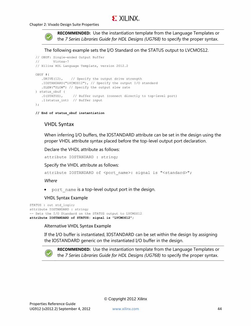
// Sets the I/O Standard on the STATUS output to LVCMOS12
(* IOSATNDARD = "LVCMOS12" *) output STATUS,
Alternative Verilog Syntax Example
If the I/O buffer is instantiated, IOSATNDARD can be set within the design by assigning
the IOSTANDARD parameter on the instantiated I/O buffer in the design.
Chapter 2: Vivado Design Suite Properties
© Copyright 2012 Xilinx
Properties Reference Guide UG912 (v2012.2) September 4, 2012 www.xilinx.com 44
RECOMMENDED: Use the instantiation template from the Language Templates or
the 7 Series Libraries Guide for HDL Designs (UG768) to specify the proper syntax.
The following example sets the I/O Standard on the STATUS output to LVCMOS12.
// OBUF: Single-ended Output Buffer
// Virtex-7
// Xilinx HDL Language Template, version 2012.2
OBUF #(
.DRIVE(12), // Specify the output drive strength
.IOSTANDARD("LVCMOS12"), // Specify the output I/O standard
.SLEW("SLOW") // Specify the output slew rate
) status_obuf (
.O(STATUS), // Buffer output (connect directly to top-level port)
.I(status_int) // Buffer input
);
// End of status_obuf instantiation
VHDL Syntax
When inferring I/O buffers, the IOSTANDARD attribute can be set in the design using the
proper VHDL attribute syntax placed before the top-level output port declaration.
Declare the VHDL attribute as follows:
attribute IOSTANDARD : string;
Specify the VHDL attribute as follows:
attribute IOSTANDARD of <port_name>: signal is "<standard>";
Where
port_name is a top-level output port in the design.
VHDL Syntax Example
STATUS : out std_logic;
attribute IOSTANDARD : string;
-- Sets the I/O Standard on the STATUS output to LVCMOS12
attribute IOSTANDARD of STATUS: signal is "LVCMOS12";
Alternative VHDL Syntax Example
If the I/O buffer is instantiated, IOSTANDARD can be set within the design by assigning
the IOSTANDARD generic on the instantiated I/O buffer in the design.
RECOMMENDED: Use the instantiation template from the Language Templates or
the 7 Series Libraries Guide for HDL Designs (UG768) to specify the proper syntax.
IOSTANDARD
© Copyright 2012 Xilinx
Properties Reference Guide UG912 (v2012.2) September 4, 2012 www.xilinx.com 45
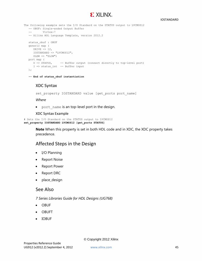
The following example sets the I/O Standard on the STATUS output to LVCMOS12
-- OBUF: Single-ended Output Buffer
-- Virtex-7
-- Xilinx HDL Language Template, version 2012.2
status_obuf : OBUF
generic map (
DRIVE => 12,
IOSTANDARD => "LVCMOS12",
SLEW => "SLOW")
port map (
O => STATUS, -- Buffer output (connect directly to top-level port)
I => status_int -- Buffer input
);
-- End of status_obuf instantiation
XDC Syntax
set_property IOSTANDARD value [get_ports port_name]
Where
port_name is an top-level port in the design.
XDC Syntax Example
# Sets the I/O Standard on the STATUS output to LVCMOS12
set_property IOSTANDARD LVCMOS12 [get_ports STATUS]
Note When this property is set in both HDL code and in XDC, the XDC property takes
precedence.
Affected Steps in the Design
I/O Planning
Report Noise
Report Power
Report DRC
place_design
See Also
7 Series Libraries Guide for HDL Designs (UG768)
OBUF
OBUFT
IOBUF
Chapter 2: Vivado Design Suite Properties
© Copyright 2012 Xilinx
Properties Reference Guide UG912 (v2012.2) September 4, 2012 www.xilinx.com 46
IOBUF_DCIEN
IOBUF_INTERM_DISABLE
For legal values, see the SelectIO Resources User Guide.
KEEP_HIERARCHY
© Copyright 2012 Xilinx
Properties Reference Guide UG912 (v2012.2) September 4, 2012 www.xilinx.com 47
KEEP_HIERARCHY
KEEP_HIERARCHY directs the tool to retain a user hierarchy in the design so that
optimization does not occur across its boundary. This can be used to assist
floorplanning, analysis, and debug efforts, but may inhibit optimization. This can result in
a larger, slower design.
RECOMMENDED: To avoid these negative effects, register all outputs of a module
instance in which a KEEP_HIERARCHY is attached. To be most effective, apply this
attribute before synthesis.
Architecture Support
All architectures
Applicable Elements
Cells (get_cells)
User defined instance
Values
FALSE (default)
Allow optimization across hierarchy.
TRUE
Preserve hierarchy by not allowing any optimization across hierarchy boundary.
Syntax and Syntax Examples
IMPORTANT: Before copying syntax or coding examples from this PDF document
for insertion into your code, see Copying Syntax and Coding Examples from PDF
Documents in the Introduction to this guide.
Verilog Syntax
Place the Verilog attribute immediately before the user hierarchy instantiation in the
design:
(* KEEP_HIERARCHY = "{TRUE|FALSE}" *)
Chapter 2: Vivado Design Suite Properties
© Copyright 2012 Xilinx
Properties Reference Guide UG912 (v2012.2) September 4, 2012 www.xilinx.com 48
Verilog Syntax Example
// Preserve the hierarchy of instance CLK1_rst_sync
(* KEEP_HIERARCHY = "TRUE" *) reset_sync #(
.STAGES(5)
) CLK1_rst_sync (
.RST_IN(RST | ~LOCKED),
.CLK(clk1_100mhz),
.RST_OUT(rst_clk1)
);
VHDL Syntax
Declare the VHDL attribute as follows:
attribute KEEP_HIERARCHY : string;
Specify the VHDL attribute as follows:
attribute KEEP_HIERACHRY of name: label is "{TRUE|FALSE}";
Where
name is either the instance name of a user defined instance in the design.
VHDL Syntax Example
attribute KEEP_HIERARCHY : string;
-- Preserve the hierarchy of instance CLK1_rst_sync
attribute KEEP_HIERARCHY of CLK1_rst_sync: label is "TRUE";
…
CLK1_rst_sync : reset_sync
PORT MAP (
RST_IN => RST_LOCKED,
CLK => clk1_100mhz,
RST_OUT => rst_clk1
);
XDC Syntax
set_property KEEP_HIERARCHY {TRUE|FALSE} [get_cells instance_name]
Where
instance_name is a register instances in the design.
XDC Syntax Example
# Preserve the hierarchy of instance CLK1_rst_sync
set_property KEEP_HIERARCHY TRUE [get_cells CLK1_rst_sync]
Affected Steps in the Design
synth_design
opt_design
phys_opt_design
floorplanning
LOC
© Copyright 2012 Xilinx
Properties Reference Guide UG912 (v2012.2) September 4, 2012 www.xilinx.com 49
LOC
LOC specifies a specific placement of a primitive component within the device.
Architecture Support
All architectures
Applicable Elements
Cells (get_cells)
Any primitive
Values
Site name (for example, SLICE_X15Y14 or RAMB18_X6Y9)
Syntax and Syntax Examples
IMPORTANT: Before copying syntax or coding examples from this PDF document
for insertion into your code, see Copying Syntax and Coding Examples from PDF
Documents in the Introduction to this guide.
Verilog Syntax
Place the Verilog attribute immediately before the instantiation of a component in the
design.
Alternative Verilog Syntax Example
The Verilog attribute can be placed before the reg declaration of an inferred register,
SRL, or LUTRAM in the design when that reg can be placed into a single device site:
(* LOC = "site_name" *)
// Designates placed_reg to be placed in Slice site SLICE_X0Y0
(* LOC = "SLICE_X0Y0" *) reg placed_reg;
VHDL Syntax
Declare the VHDL attribute as follows:
attribute LOC : string;
For an instantiated instance, specify the VHDL attribute as follows:
attribute LOC of instance_name : label is "site_name";
Chapter 2: Vivado Design Suite Properties
© Copyright 2012 Xilinx
Properties Reference Guide UG912 (v2012.2) September 4, 2012 www.xilinx.com 50
Where
instance_name is the instance name of an instantiated primitive.
VHDL Syntax Example
-- Designates instantiated register instance placed_reg to be placed
-- in Slice site SLICE_X0Y0
attribute LOC of placed_reg : label is "SLICE_X0Y0";
For an inferred instance, Specify the VHDL attribute as follows:
attribute LOC of signal_name : signal is "site_name";
Where
signal_name is the signal name of an inferred primitive which can be placed into a
single site.
VHDL Syntax Example
-- Designates inferred register placed_reg to be placed in Slice site SLICE_X0Y0
attribute LOC of placed_reg : signal is "SLICE_X0Y0";
XDC Syntax
set_property LOC site_name [get_cells instance_name]
Where
instance_name is a primitive instance in the design.
XDC Syntax Example
# Designates placed_reg to be placed in Slice site SLICE_X0Y0
set_property LOC SLICE_X0Y0 [get_cells placed_reg]
Note When this property is set in both HDL code and in XDC, the XDC property takes
precedence.
Affected Steps in the Design
Design Floorplanning
place_design
See Also
BEL
PACKAGE_PIN
LUTNM
© Copyright 2012 Xilinx
Properties Reference Guide UG912 (v2012.2) September 4, 2012 www.xilinx.com 51
LUTNM
LUTNM instructs the tool to place two LUT5, SRL16, or LUTRAM components with
compatible inputs into the same LUT6 site. The LUTNM must be specified in pairs, with
two of these specified on compatible instance types with the same group name.
Difference Between LUTNM and HLUTNM
LUTNM can be used to combine two LUTs that exist in different user hierarchy.
Use LUTNM to group two LUTs that exist in the same user hierarchy.
Architecture Support
All architectures
Applicable Elements
Cells (get_cells)
LUTs (LUT1, LUT2, LUT3, LUT4, LUT5)
SRLs (SRL16E)
LUTRAMs (RAM32X1D, RAM32X1S)
Values
A unique group name
Syntax and Syntax Examples
IMPORTANT: Before copying syntax or coding examples from this PDF document
for insertion into your code, see Copying Syntax and Coding Examples from PDF
Documents in the Introduction to this guide.
Verilog Syntax
Place the Verilog attribute immediately before the instantiation of a LUT in the design.
The Verilog attribute must be used in pairs in the same logical hierarchy in the design.
(* LUTNM = "group_name" *)
Chapter 2: Vivado Design Suite Properties
© Copyright 2012 Xilinx
Properties Reference Guide UG912 (v2012.2) September 4, 2012 www.xilinx.com 52
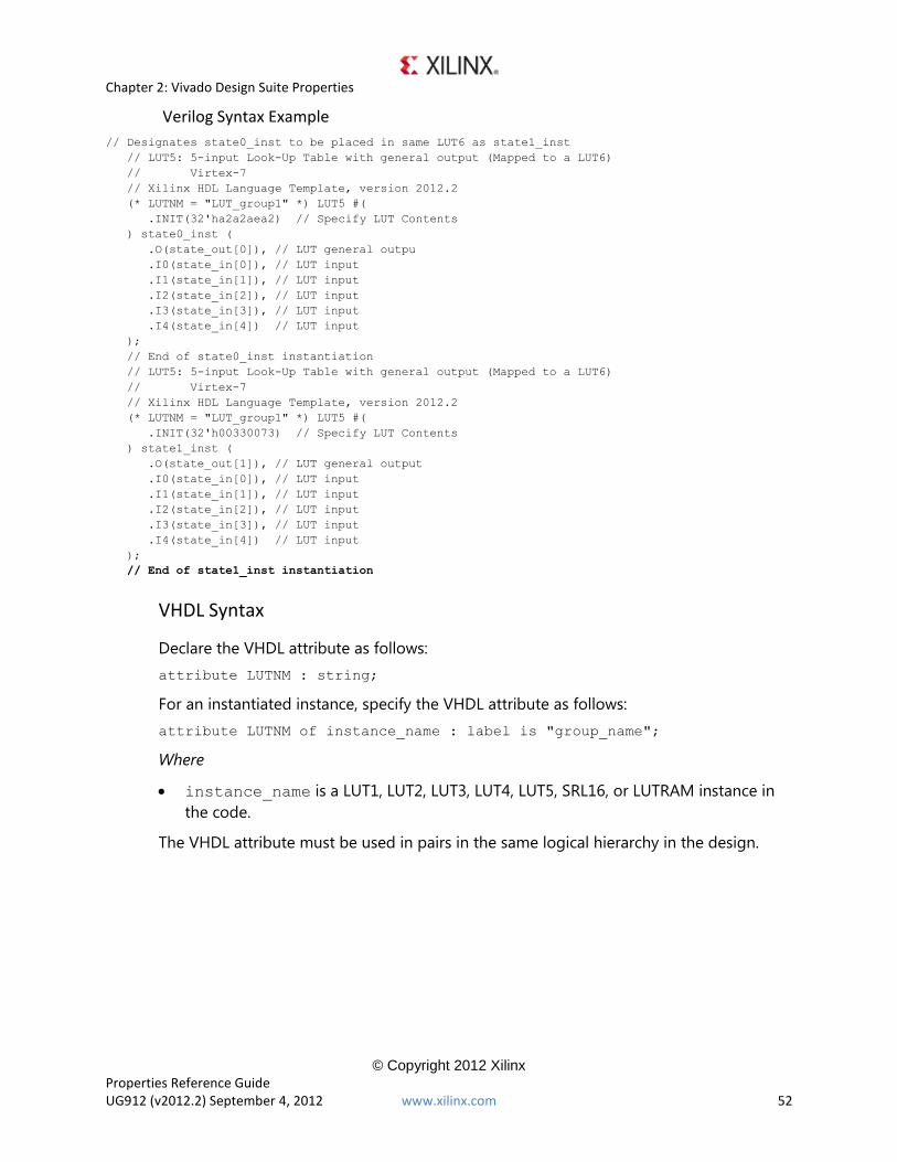
Verilog Syntax Example
// Designates state0_inst to be placed in same LUT6 as state1_inst
// LUT5: 5-input Look-Up Table with general output (Mapped to a LUT6)
// Virtex-7
// Xilinx HDL Language Template, version 2012.2
(* LUTNM = "LUT_group1" *) LUT5 #(
.INIT(32'ha2a2aea2) // Specify LUT Contents
) state0_inst (
.O(state_out[0]), // LUT general outpu
.I0(state_in[0]), // LUT input
.I1(state_in[1]), // LUT input
.I2(state_in[2]), // LUT input
.I3(state_in[3]), // LUT input
.I4(state_in[4]) // LUT input
);
// End of state0_inst instantiation
// LUT5: 5-input Look-Up Table with general output (Mapped to a LUT6)
// Virtex-7
// Xilinx HDL Language Template, version 2012.2
(* LUTNM = "LUT_group1" *) LUT5 #(
.INIT(32'h00330073) // Specify LUT Contents
) state1_inst (
.O(state_out[1]), // LUT general output
.I0(state_in[0]), // LUT input
.I1(state_in[1]), // LUT input
.I2(state_in[2]), // LUT input
.I3(state_in[3]), // LUT input
.I4(state_in[4]) // LUT input
);
// End of state1_inst instantiation
VHDL Syntax
Declare the VHDL attribute as follows:
attribute LUTNM : string;
For an instantiated instance, specify the VHDL attribute as follows:
attribute LUTNM of instance_name : label is "group_name";
Where
instance_name is a LUT1, LUT2, LUT3, LUT4, LUT5, SRL16, or LUTRAM instance in
the code.
The VHDL attribute must be used in pairs in the same logical hierarchy in the design.
LUTNM
© Copyright 2012 Xilinx
Properties Reference Guide UG912 (v2012.2) September 4, 2012 www.xilinx.com 53
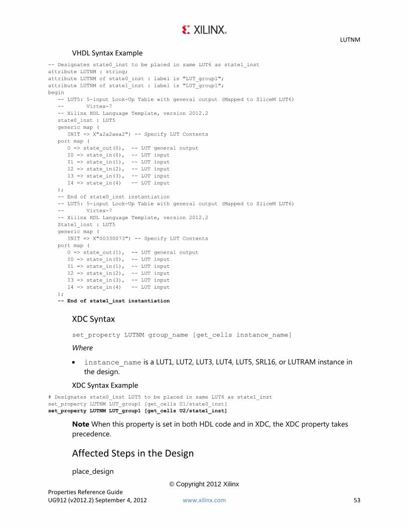
VHDL Syntax Example
-- Designates state0_inst to be placed in same LUT6 as state1_inst
attribute LUTNM : string;
attribute LUTNM of state0_inst : label is "LUT_group1";
attribute LUTNM of state1_inst : label is "LUT_group1";
begin
-- LUT5: 5-input Look-Up Table with general output (Mapped to SliceM LUT6)
-- Virtex-7
-- Xilinx HDL Language Template, version 2012.2
state0_inst : LUT5
generic map (
INIT => X"a2a2aea2") -- Specify LUT Contents
port map (
O => state_out(0), -- LUT general output
I0 => state_in(0), -- LUT input
I1 => state_in(1), -- LUT input
I2 => state_in(2), -- LUT input
I3 => state_in(3), -- LUT input
I4 => state_in(4) -- LUT input
);
-- End of state0_inst instantiation
-- LUT5: 5-input Look-Up Table with general output (Mapped to SliceM LUT6)
-- Virtex-7
-- Xilinx HDL Language Template, version 2012.2
State1_inst : LUT5
generic map (
INIT => X"00330073") -- Specify LUT Contents
port map (
O => state_out(1), -- LUT general output
I0 => state_in(0), -- LUT input
I1 => state_in(1), -- LUT input
I2 => state_in(2), -- LUT input
I3 => state_in(3), -- LUT input
I4 => state_in(4) -- LUT input
);
-- End of state1_inst instantiation
XDC Syntax
set_property LUTNM group_name [get_cells instance_name]
Where
instance_name is a LUT1, LUT2, LUT3, LUT4, LUT5, SRL16, or LUTRAM instance in
the design.
XDC Syntax Example
# Designates state0_inst LUT5 to be placed in same LUT6 as state1_inst
set_property LUTNM LUT_group1 [get_cells U1/state0_inst]
set_property LUTNM LUT_group1 [get_cells U2/state1_inst]
Note When this property is set in both HDL code and in XDC, the XDC property takes
precedence.
Affected Steps in the Design
place_design
Chapter 2: Vivado Design Suite Properties
© Copyright 2012 Xilinx
Properties Reference Guide UG912 (v2012.2) September 4, 2012 www.xilinx.com 54
See Also
HLUTNM
MARK_DEBUG
© Copyright 2012 Xilinx
Properties Reference Guide UG912 (v2012.2) September 4, 2012 www.xilinx.com 55
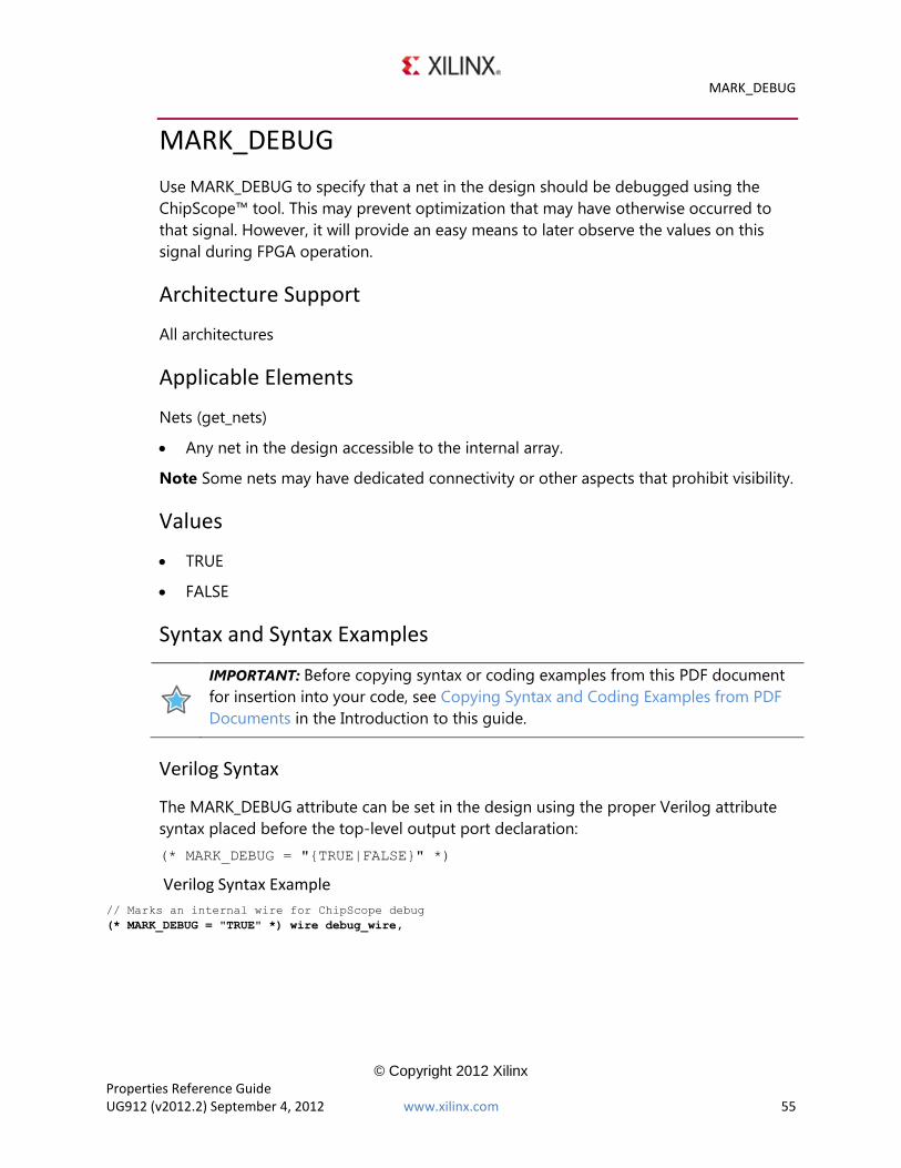
MARK_DEBUG
Use MARK_DEBUG to specify that a net in the design should be debugged using the
ChipScope™ tool. This may prevent optimization that may have otherwise occurred to
that signal. However, it will provide an easy means to later observe the values on this
signal during FPGA operation.
Architecture Support
All architectures
Applicable Elements
Nets (get_nets)
Any net in the design accessible to the internal array.
Note Some nets may have dedicated connectivity or other aspects that prohibit visibility.
Values
TRUE
FALSE
Syntax and Syntax Examples
IMPORTANT: Before copying syntax or coding examples from this PDF document
for insertion into your code, see Copying Syntax and Coding Examples from PDF
Documents in the Introduction to this guide.
Verilog Syntax
The MARK_DEBUG attribute can be set in the design using the proper Verilog attribute
syntax placed before the top-level output port declaration:
(* MARK_DEBUG = "{TRUE|FALSE}" *)
Verilog Syntax Example
// Marks an internal wire for ChipScope debug
(* MARK_DEBUG = "TRUE" *) wire debug_wire,
Chapter 2: Vivado Design Suite Properties
© Copyright 2012 Xilinx
Properties Reference Guide UG912 (v2012.2) September 4, 2012 www.xilinx.com 56
VHDL Syntax
The MARK_DEBUG attribute can be set in the design using the proper VHDL attribute
syntax placed before the top-level output port declaration.
Declare the VHDL attribute as follows:
attribute MARK_DEBUG : string;
Specify the VHDL attribute as follows:
attribute MARK_DEBUG of signal_name : signal is “{TRUE|FALSE}”;
Where
signal_name is an internal signal in the design.
VHDL Syntax Example
signal debug_wire : std_logic;
attribute MARK_DEBUG : string;
-- Marks an internal wire for ChipScope debug
attribute MARK_DEBUG of debug_wire : signal is “TRUE”;
XDC Syntax
set_property MARK_DEBUG value [get_nets net_name]
Where
net_name is a signal name in the design.
XDC Syntax Example
# Marks an internal wire for ChipScope debug
set_property MARK_DEBUG TRUE [get_nets debug_wire]
Affected Steps in the Design
place_design
ChipScope
See Also
DONT_TOUCH
PACKAGE_PIN
© Copyright 2012 Xilinx
Properties Reference Guide UG912 (v2012.2) September 4, 2012 www.xilinx.com 57
PACKAGE_PIN
PACKAGE_PIN specifies a specific placement of a top-level port in the logical design to a
physical package pin on the device.
Architecture Support
All architectures
Applicable Elements
Ports (get_ports)
Any top-level port
Values
Package pin name
Syntax and Syntax Examples
IMPORTANT: Before copying syntax or coding examples from this PDF document
for insertion into your code, see Copying Syntax and Coding Examples from PDF
Documents in the Introduction to this guide.
Verilog Syntax
Place the Verilog attribute immediately before the port declaration in the design:
(* PACKAGE_PIN = "pin_name" *)
Verilog Syntax Example
// Designates port CLK to be placed on pin B26
(* PACKAGE_PIN = "B26" *) input CLK;
VHDL Syntax
Declare the VHDL attribute as follows:
attribute PACKAGE_PIN : string;
Specify the VHDL attribute as follows:
attribute PACKAGE_PIN of port_name : signal is "pin_name";
VHDL Syntax Example
-- Designates CLK to be placed on pin B26
attribute PACKAGE_PIN of CLK : signal is "B26";
Chapter 2: Vivado Design Suite Properties
© Copyright 2012 Xilinx
Properties Reference Guide UG912 (v2012.2) September 4, 2012 www.xilinx.com 58
XDC Syntax
set_property PACKAGE_PIN pin_name [get_ports port_name]
XDC Syntax Example
# Designates CLK to be placed on pin B26
set_property PACKAGE_PIN B26 [get_ports CLK]
Note When this property is set in both HDL code and in XDC, the XDC property takes
precedence.
Affected Steps in the Design
Pin planning
place_design
See Also
LOC
PROHIBIT
© Copyright 2012 Xilinx
Properties Reference Guide UG912 (v2012.2) September 4, 2012 www.xilinx.com 59
PROHIBIT
PROHIBIT specifies that a particular pin or site in the chip cannot be used for placement
of the design.
Architecture Support
All architectures
Applicable Elements
Sites (get_sites)
BELs (get_bels)
Values
1
Syntax and Syntax Examples
IMPORTANT: Before copying syntax or coding examples from this PDF document
for insertion into your code, see Copying Syntax and Coding Examples from PDF
Documents in the Introduction to this guide.
Verilog Syntax
Not applicable
VHDL Syntax
Not applicable
XDC Syntax
set_property PROHIBIT 1 [get_sites site]
XDC Syntax Example
# Prohibit the use of package pin Y32
set_property prohibit 1 [get_sites Y32]
Affected Steps in the Design
I/O planning
place_design
Chapter 2: Vivado Design Suite Properties
© Copyright 2012 Xilinx
Properties Reference Guide UG912 (v2012.2) September 4, 2012 www.xilinx.com 60
SLEW
SLEW specifies output buffer slew rate for output buffers configured with I/O standards
that support programmable output slew rates.
Architecture Support
All architectures
Applicable Elements
Ports (get_ports)
Output or bi-directional ports connected
Cells (get_cells)
Output Buffers (all OBUF variants)
Values
SLOW (default)
FAST
Syntax and Syntax Examples
IMPORTANT: Before copying syntax or coding examples from this PDF document
for insertion into your code, see Copying Syntax and Coding Examples from PDF
Documents in the Introduction to this guide.
Verilog Syntax
When inferring I/O buffers, the SLEW attribute can be set in the design using the proper
Verilog attribute syntax placed before the top-level output port declaration:
(* DRIVE = "{SLOW|FAST}" *)
Verilog Syntax Example
// Sets the Slew rate to be FAST
(* SLEW = "FAST" *) output FAST_DATA,
Alternative Verilog Syntax Example
If the output or bi-directional buffer is instantiated, SLEW can be set within the design by
assigning the SLEW parameter on the instantiated output buffer in the design.
SLEW
© Copyright 2012 Xilinx
Properties Reference Guide UG912 (v2012.2) September 4, 2012 www.xilinx.com 61
RECOMMENDED: Use the instantiation template from the Language Templates or
the 7 Series Libraries Guide for HDL Designs (UG768) to specify the proper syntax.
The following example sets the slew rate on the OBUF instance named
fast_data_obuf to FAST:
// OBUF: Single-ended Output Buffer
// Virtex-7
// Xilinx HDL Language Template, version 2012.2
OBUF #(
.DRIVE(12), // Specify the output drive strength
.IOSTANDARD("DEFAULT"), // Specify the output I/O standard
.SLEW("FAST") // Specify the output slew rate
) fast_data_obuf (
.O(FAST_DATA), // Buffer output (connect directly to top-level port)
.I(fast_data_int) // Buffer input
);
// End of fast_data_obuf instantiation
VHDL Syntax
When inferring I/O buffers, the SLEW attribute can be set in the design using the proper
VHDL attribute syntax placed before the top-level output port declaration.
Declare the VHDL attribute as follows:
attribute SLEW : string;
Specify the VHDL attribute as follows:
attribute SLEW of port_name : signal is value;
Where
port_name is a top-level output port in the design.
VHDL Syntax Example
FAST_DATA : out std_logic;
attribute SLEW : string;
-- Sets the Slew rate to be FAST
attribute SLEW of STATUS : signal is “FAST”;
Alternative VHDL Syntax Example
If the output or bi-directional buffer is instantiated, SLEW can be set within the design by
assigning the SLEW generic on the instantiated output buffer in the design.
RECOMMENDED: Use the instantiation template from the Language Templates or
the 7 Series Libraries Guide for HDL Designs (UG768) to specify the proper syntax.
Chapter 2: Vivado Design Suite Properties
© Copyright 2012 Xilinx
Properties Reference Guide UG912 (v2012.2) September 4, 2012 www.xilinx.com 62
The following example sets the slew rate on the OBUF instance named
fast_data_obuf to FAST.
-- OBUF: Single-ended Output Buffer
-- Virtex-7
-- Xilinx HDL Language Template, version 2012.2
Fast_data_obuf : OBUF
generic map (
DRIVE => 12,
IOSTANDARD => "DEFAULT",
SLEW => "FAST")
port map (
O => FAST_DATA, -- Buffer output (connect directly to top-level port)
I => fast_data_int -- Buffer input
);
-- End of fast_data_obuf instantiation
XDC Syntax
set_property SLEW value [get_ports port_name]
Where
port_name is an output or bi-directional port in the design.
XDC Syntax Example
# Sets the Slew rate to be FAST
set_property SLEW FAST [get_ports FAST_DATA]
Note When this property is set in both HDL code and in XDC, the XDC property takes
precedence.
Affected Steps in the Design
I/O Planning
Report Noise
Report Power
See Also
7 Series Libraries Guide for HDL Designs (UG768)
OBUF
OBUFT
IOBUF
IOBUF_DCIEN
IOBUF_INTERM_DISABLE
VCCAUX_IO
© Copyright 2012 Xilinx
Properties Reference Guide UG912 (v2012.2) September 4, 2012 www.xilinx.com 63
VCCAUX_IO
VCCAUXIO specifies the operating voltage of the VCCAUX_IO rail for a given I/O.
Architecture Support
All architectures on High Performance (HP) bank I/O only
Applicable Elements
Ports (get_ports)
Cells (get_cells)
I/O buffers
Values
DONTCARE (default)
NORMAL
HIGH
Syntax and Syntax Examples
IMPORTANT: Before copying syntax or coding examples from this PDF document
for insertion into your code, see Copying Syntax and Coding Examples from PDF
Documents in the Introduction to this guide.
Verilog Syntax
The VCCAU_IO attribute can be set in the design using the proper Verilog attribute
syntax placed before the top-level output port declaration:
(* VCCAUXIO = "{DONTCARE|NORMAL|HIGH}" *)
Verilog Syntax Example
// Specifies a “HIGH” voltage for the VCCAUX_IO rail connected to this I/O
(* VCCAUX_IO = "HIGH" *) input ACT3,
VHDL Syntax
The VCCAUX_IO attribute can be set in the design using the proper VHDL attribute
syntax placed before the top-level output port declaration.
Declare the VHDL attribute as follows:
attribute VCCAUX_IO : string;
Chapter 2: Vivado Design Suite Properties
© Copyright 2012 Xilinx
Properties Reference Guide UG912 (v2012.2) September 4, 2012 www.xilinx.com 64
Specify the VHDL attribute as follows:
attribute VCCAUX_IO of port_name : signal is value;
Where
port_name is a top-level port in the design.
VHDL Syntax Example
ACT3 : in std_logic;
attribute VCCAUX_IO : string;
-- Specifies a “HIGH” voltage for the VCCAUX_IO rail connected to this I/O
attribute VCCAUX_IO of ACT3 : signal is “HIGH”;
XDC Syntax
set_property VCCAUX_IO value [get_ports port_name]
Where
port_name is a top-level port in the design.
XDC Syntax Example
# Specifies a “HIGH” voltage for the VCCAUX_IO rail connected to this I/O
set_property VCCAUX_IO HIGH [get_ports ACT3]
Note When this property is set in both HDL code and in XDC, the XDC property takes
precedence.
Affected Steps in the Design
I/O Planning
place_design
Report Power
© Copyright 2012 Xilinx
Properties Reference Guide UG912 (v2012.2) September 4, 2012 www.xilinx.com 65
Appendix A
Additional Resources
Xilinx Resources
For support resources such as Answers, Documentation, Downloads, and Forums, see the
Xilinx® Support website at:
www.xilinx.com/support
For a glossary of technical terms used in Xilinx documentation, see:
www.xilinx.com/company/terms.htm
Solution Centers
See the Xilinx Solution Centers for support on devices, software tools, and intellectual
property at all stages of the design cycle. Topics include design assistance, advisories,
and troubleshooting tips.
References
These documents provide supplemental material useful with this guide:
Vivado Design Suite 2012.2 Documentation,
www.xilinx.com/support/documentation/dt_vivado_vivado2012-2.htm