Embed Size (px)
Citation preview


.;^ LIBRARY
^ . vj^; f
A Digital Signal Processing Solution for
Multichannel Base Stations
by
Scott Leyonhjelm, B.Eng (Hons.)
A thesis submitted for the degree of
Doctor of Philosophy
at
Victoria University of Technology
November, 1995.
Department of Electrical and Electronic Engineering,
PO BOX 14428, MCMC, 8001,
Australia.

FTS THESIS 621.38A5 LEY 30001005034048 Leyonhjelm, Scott A digital signal processing solution for multichannel

Abstract
Radio communication systems of the future will require a large increase in user capacity.
To achieve this, cell sizes will reduce and the number of base stations will increase.
Current base station architectures use analogue combining techniques which are
expensive, voluminous and inflexible. This thesis investigates a Digital Signal Processing
(DSP) solution which produces a cheaper, smaller and more flexible multichannel base
station transmitter design. The main design challenges of the new DSP low power
combining architecture are the multichannel combining algorithm, the frequency
translation of the multichannel signal to radio frequency, the Digital to Analogue
Conversion (DAC) interface and the wideband ultra-linear power amplifier. This thesis
considers the pre-power amplifier stages.
Combining the channels in a digital signal processing environment provides considerable
flexibility, but the computational requirements are very high. The minimisation of
computational load is achieved by combining the channels at baseband with efficient
algorithms.
Four upconversion techniques, currentiy used in single channel applications, are
investigated for use in a wideband multichannel environment. Comparisons reveal that
analogue direct upconversion currently provides the most attractive solution because a
lower performance DAC is required and less computation is needed. However, amplitude
and phase mismatch between the In Phase and Quadrature circuits cause undesired
sideband responses that exceed radio system specifications. A novel adaptive
compensation method leads to an improved performance and a lower computational
overhead compared to previous techniques.
Multichannel radio systems can only tolerate very low harmonic and intermodulation
products and the DAC is a major source of these spurious responses. A new
implementation of bandlimited dithering is shown to improve the performance of the DAC
by 2 to 4 dB, with only a small increase in hardware.

Preface
This thesis describes the development of a low power combining digital signal processing
architecture for future radio base station transmitters. The goal of the project is to produce
a base station that is small, cheap and greatly more flexible than the conventional base
station design.
The idea for the low power combining architecture was described in the 1980's and its
advantages over the conventional design have since been well recognised. However, four
technological challenges have impeded the immediate development of the digital signal
processing low power combining technique:
• the large amount of computation required to combine multiple channels in a digital signal processor,
• the high degree of linearity needed to convert the multichannel signal from baseband to RF,
• the high speed and precision of the DAC required to convert the digital multichannel signal to an analogue signal, and
• the ultra-linear power amplifier needed to boost the power level of the multichannel signal for radio frequency transmission.
The ultra-linear power amplifier is seen as the most difficult design obstacle to overcome
and most researchers and manufacturers of radio base stations have, and still are, focusing
much research and deyelopment on this area. Through the use of advanced linearisation
techniques, feedforward, feedback and predistortion, a sufficiently linear and wideband
power amplifier has been developed. These developments haye only occurred since the
thesis began in 1991 although the power amplifier is still limited in total power output.
The objective of the thesis has been to concentrate on the design challenges of the pre-
power amplifier stages. A detailed examination of the combining of multiple channels and
the upconversion of the multichannel signal to RF provide clarification of the pertinent
issues regarding a digital signal processing base station. These discussions lead to the
choice of the analogue direct upconversion technique. A new compensation algorithm
required to ensure that this upconversion technique meets the radio system specifications

Ill
is developed and has been presented in two papers:
I Leyonhjelm, S.A., Faulkner, M. & Macleod, J., "The Effect of
Reconstmction Filter Mismatch in a Digital Signal Processing Multichannel
Combiner", IEEE Intemational Conference on Universal Wireless Access,
World Congress Centre, Melbourne, Australia, April 18-19, 1994, pp 25-30.
n Leyonhjelm, S. & Faulkner, M., "DSP Combining and Direct Conversion for
Multichannel Transmitters", 43'"' lEEEA^TS Vehicular Technology
Conference, Stockholm, Sweden, June 7-10, 1994, Vol. 1 of 3,pp 494-498.
The compensation technique is sensitive to frequency dependant mismatch between the In
Phase and Quadrature reconstmction filters and this has been analysed in a third
publication:
III Leyonhjelm, S.A. & Faulkner, M., "The Effect of Reconstmction Filters on
Direct Upconversion in a Multichannel Environment", IEEE Transactions on
Vehicular Technology, Vol. 44, No. 1, Feb. 1995, pp 95-102.
Papers I and III have an error in Eqns. (5) and (17) respectively, but it does not affect either
conclusion. The error has been corrected in this thesis, Eqn. (4.17).
The digital to analogue converter quantisation nonlinearity introduces harmonic and
intermodulation products, which are troublesome in a multichannel base station.
Improving the DAC linearity has been approached from the point of view that it is a black
box and an external algorithm has been developed to improve the performance of the
DAC. Although the performance increase is small, 2 to 4 dB, it has been implemented
with minimal increase in hardware. The results of this technique have been accepted for
publication by the following journal:
IV Leyonhjelm, S.A., Faulkner, M., & Nilsson, P., "An Efficient Implementation
of Bandlimited Dithering", Wireless Personal Communication, Accepted for
publication on the 27 November, 1996.
It should also be mentioned that the idea of the digital signal processing base station is
currently being exploited by radio communication manufacmrers. However, due to
reasons of commercial sensitivity, much of their work remains unpublished.

IV
Acknowledgments
I would like to thank Dr. Mike Faulkner for providing much inspiration and guidance
throughout the project. Mikes endless effort, encouragement and enthusiasm has been
instmmental in me overcoming the many challenges faced during the PhD.
To Mark Briffa and Victor Taylor for their intellectually stimulating discussions and
technical assistance throughout the project. My gratitude is also extended to Zosia
Golbiowski and John Macleod for carefully reading the manuscript and commenting on
the contents and style of this thesis. Thanks also to the technical officers, Phil & Brian, the
computer doctors, Yauman & Dan, the secretaries. Rose, Shirley and Som, and the Head
of the Electrical and Electronic Engineering Department, Wally, for assisting me in varied
'matters'. Thankyou also to Patto and Haze for helping me arrange the final binding and
delivery of this thesis.
Many thanks must also go to my friends at the Department of Applied Electronics, Lund
University for their open and warm hospitality, and providing the necessary resources
needed to design and fabricate the Application Specific Integrated Circuits (ASIC's).
Special thanks must go to Mats Johansson for his efforts in helping me to organise my trip
to Sweden and being a generous host whilst I was at Lund University, and Peter Nilsson
for teaching me the intricacies of the ASIC development tools.
To David Pope of Signal Processing Associates for his enlightening technical discussions
and lending me digital to analogue converter hardware that was developed by his
company.
The research described in this report obtained financial support from Victoria University
of Technology in the form of a postgraduate scholarship and tutorial work that enabled me
to complete the thesis without financial burden. Additional funding was also obtained
from the following sources:
• The Secomb scholarship that assisted in conference expenses whilst at VTC 94 in Stockholm, Sweden.
The DTTAC Bilateral Science and Technology Co-operation Program which enabled me to travel to Lund University, Sweden to complete the eight weeks necessary to build the ASIC.
• The ATERB Research Project Grant for assisting in the purchasing of the TMSC40 development system.

I am also very appreciative of the patience and support that Rachel has showed during the
final stages of this work. Finally, and most importantiy, I would like to thank my parents,
Josi and Max, for providing immense support throughout all my lifes endeavours. They
are the rock on which I stand.
Scott Leyonhjelm.
November, 1995.

\ 1
List of Principal Symbols and Abbreviations
Symbol or Abbreviation Description
ak(t) ACI ADC
ANT-TXisoiation ASIC
RW " " cavity
BW " " meas BW,y3 BWjdB %BW
Amplitude modulation of channel k Adjacent Channel Interference Analogue to Digital Converter Antenna to transmitter isolation Application Specific Integrated Circuit
3 dB bandwidth of the cavity filter Bandwidth of the channel Bandwidth of the measurement bandpass filter Switching bandwidth of the wireless system 3dB bandwidth of a bandpass filter Fractional 3dB bandwidth of a bandpass filter
First Used in Section
2.2.1 T O T
5.3.1.1 2.2.3 6.4
2.2.4.1 3.2 3.3.1.2 3.2 3.3.2.1 3.3.2.1
c CpTT CGSM
^ADU C|p
Cm C40 CaNAD CNRmuiti CRI
Peak to peak amplitude of uniform dither 5.3.1.1 Computation power of the polyphase FFT combining algorithm. 3.2.2.1 Computation power for the GSM radio system 3.2.2.2 Computation power of Analogue Direst Upconversion 3.3.3.1 Computation power of Digital IF Upconversion 3.3.1.1 Complex co-efficient 4.2 Texas Instrument general purpose DSP 3.2.1 Carrier to Noise And Distortion ratio 6.3 Multichannel carrier to noise power ratio 3.3.1.2 The Control and Radio Interface 1.1
dBc dBm d(n) DAC DC DCS DDS DR DSP
Absolute power level below the reference carrier component Absolute power level with respect to a 1 mW reference Discrete dither signal Digital to Analog Converter Direct Current Digital Communication System Direct Digital Synthesis Dielectric Resonator Digital Signal Processing
6.2.1 2.4.2 1.2 2.1 3.2.2.2 3.3.1.2 1.2
e(t) Error vector caused by mismatch b/n the I&Q reconstruction filters 4.3.2
alias n
fiF fk Af Af alias Afcs Afy f 's-mod f 's-comb fs f 'so FDM FFSK
Centre frequency of the n alias Centre frequency Data bit rate Intermediate frequency of a multichannel signal Centre frequency of channel k Frequency offset from centre frequency Separation between adjacent aliases Channel frequency spacing Filter Transition bandwidth Modulation sampling frequency of a single channel Combining sampling frequency of a multichannel signal Sampling frequency Output sampling frequency - refers to DAC interface Frequency Division Multiplex Fast Frequency Shift Keying
3.3.2.1 2.2.4.1 3.2.2.2 3.3.1 2.2.1 2.2.4.1 3.3.2.1 2.3.1 3.2.2.1 3.2.1 3.2.1 3.2.2.1 3.3.3.1 2.2 3.2.2.1

List of Principal Symbols and Abbreviations VI1
FFT FPGA FSR
g(X)
^amp GSM
h(m), hk H (Af) cavity
I
^isolator
^cavity IF IL
^'^cavity
• '-'isolator IM
Fast Frequency Transform Field Progranmiable Gate Array Full Scale Range of a DAC
DAC quantisation transfer function
DAC average quantisation function Gain of an amplifier Global Speciale Mobile
Impulse response (tap co-efficients) of a digital FIR filter Transfer function of the cavity filter near resonance
In Phase component of a complex signal Isolation (Reverse loss) of the ferrite isolator Isolation (Reverse loss) of the cavity resonator Intermediate Frequency Insertion loss Insertion (forward) loss of the cavity resonator Equivalent insertion loss of (Ncomb"') cavities Insertion (forward) loss of the ferrite isolator InterModulation
3.2.2.1 3.2.1 3.3.1.2
5.2.1
5.4 2.2.3 2.1
3.2.1 2.2.4.1
2.4.2.2 2.2.3 2.2.3 3.3.1 2.3.1 2.2.3 2.3.1 2.2.3 2.2.3
L
^feeder
'^cable LFSR LSB LUT
"itap MOPS MPT1327 MOPS
"b
^comb
Nch
OS
P G ( X ) , P U ( X ) . P T ( X ) P ' ant-mt P J av
Pc
PlM.^
"N-meas
"reflect PREV Ptav PA PCS PDF PMR
Interpolation factor 3.2.1 Forward loss of the feeder cable from the TX to the antenna 2.2.3 Forward loss of the cable in the critical harness. 2.2.3 Linear Feedback Shift Register 5.3.1.1 Least Significant Bit of a binary number 3.2.2.2 Lookup Table 3.2.2.2
Number of taps in an FIR filter. 3.2.2.1 MilHons of Operations Per Second 3.2.2.1 Private Mobile Radio (PMR) trunking system 2.1 Million of Operations Per Second 3.2.2.2
Number of bits or precision of a DAC 3.3.1.2 Number of channels combined onto one antenna 2.2.4 Total number of channels within the BWjys 3.2
Oversampling Ratio 3.2.1
Gaussian,Uniform,Triangular PDFs respectively 5.3.1.1 Power of interference signal received at the antenna. 2.2.3 Average power of a channel (carrier) 2.4.2.2 Power of a carrier signal 2.2.3 Power of the dominant 3'"' order IM product 2.2.3 Noise power measured with a bandpass filter of bandwidth - BWj g j 3.3.1.2 Reflected power of the reverse interferer incident 2.2.3 on the output of the amplifier. Power of the reverse interference signal 2.2.3 Total average power of N channels 2.4.2.2 Power Amplifier 2.2.2 Personal Communication System 2.1 Probability Density Function 5.1 Private Mobile Radio 2.1

List of Principal Symbols and Abbreviations V l l l
qe(X)
qp(n) Q Qo QL
r{t)
rk(n) rkjF(m)
R(m), R(n) R(t)
RRES RAM RF ROM RX
DAC quantisation error transfer function
DAC average quantisation error transfer function Polyphase filter impulse response. Quadrature component of a complex signal Unloaded Q factor of a cavity resonator Loaded Q factor of a cavity resonator
5.2.1
5.4.2 3.2.2.1 2.4.2.2 2.2.4.1 2.2.4.1
Vector representation of a single channel. 4.3.2 Complex baseband modulated single channel 3.2.1 Complex modulated channel, k, residing in its selected channel position 3.2.1 Complex baseband multichannel signal - discrete 3.2.1 Complex baseband multichannel signal - continuous 3.2.1 Resistance at Resonance 2.3.1 Random Access Memory 3.2.2.1 Radio Frequency 2.4.1 Read Only Memory 3.1.2.2 Receiver 1.1
Sk(t)
s(t) S(m), S(n) S(t) SAR SAW SD SF SFDR SNR SR
Single modulated channel at an IF Single modulated channel at RF Multichannel signal at RF or an IF - discrete time Multichannel signal at RF or an IF - continuous Sideband Amplitude Rejection Ratio Surface Acoustic Wave filter Spectrum Dividing filter Shape Factor of a bandpass filter Spurious Free Dynamic Range Signal to Noise Ratio Sideband Rejection ratio
2.2.1 4.3.2 3.3.1.1 3.2 4.3.2 3.3.2.1 2.2 3.3.2.1 2.4.2.2 2.4.2.2 3.3.3.2
t TX TRXl-8 1 A - 1 AjsQimjpn
«,(/)
V,(0
V ' m n v
Peak amplitude of triangular dither Transmitter GSM transmitter classes l->8 Transmitter to transmitter isolation
Desired signal vector Desired signal vector, phased 90° to M,(f)
Sideband signal vector Sideband signal vector, phased 90° to v. Half the full scale range of a DAC
(0
5.3.1,1 1.1 2.2.2 2.2.3
4.3.2 4.3.2
4.3.2 4.3.2 3.3.1.2
Wn Xi(t), Xq(t)
Xi,k(")> '^q,k(n)
Xl(t), XQ(t)
Xk
Y, 'ant
equ
' cavity
Total output noise of quantiser when dither is added In Phase and Quadrature components of r(t) In Phase and Quadrature components of x^in) In Phase and Quadrature components of R(t) Dither sample
Admittance of the antenna Equivalent admittance of (Nj-of t, -1) cavities Admittance of the cavity filter Characteristic Admittance
5.3.1.2 4.3.2 3.2 3.2 5.3
2.3.1 2.3.1 2.3.1 2.3.1
Characteristic impedance of a transmission line-nominally 50 ohm 2.3.1

List of Principal Symbols and Abbreviations ix
a(f), a Gain mismatch between the I & Q paths of the Quad. Upconverter 3.3.3.2 p(f) Normalised transfer characteristic of the Quadrature Upconverter 4.3.2 5s Stopband ripple 3.2.2.1 8p Passband ripple 3.2.2.1 A Step size or a LSB of the DAC 3.3.1.2 Og (f), C>g Phase error between the In Phase and Quadrature Paths (radians) 3.3.3.2 Q^^{t) Phase modulation of a single channel k at IF 2.2.1 6(t) Phase modulation of a single channel 4.3.2 (t)(t) Instantaneous phase of the multichannel signal 3.2 a Average power or variance of a random variable 5.2.1 fi Mean value 5.3.1.1
CONTENTS
Abstract i Preface ii Acknowledgements iv List of Principal Symbols and Abbreviations vi
1 Introduction 1
1.1 The Base Transceiver Station 2
1.2 Organisation of the Thesis 3
2 Base Station Transmitter Architectures 5
2.1 Introduction 5
2.2 Conventional Base Station Transmitter Architectures 6 2.2.1 Modulator 7 2.2.2 Power Amplifier 7 2.2.3 Ferrite Isolators 10 2.2.4 Multicoupling Networks 12
2.2.4.1 Cavity Resonators 14 2.2.4.2 Spectrum Dividing Filters 16
2.3 Limitations of a Conventional Base Station Transmitter 17 2.3.1 Minimum Channel Separation 18 2.3.2 Frequency Flexibility 21
2.3.2.1 Tunable Cavity Resonators 21 2.3.2.2 Dual Window Cavity Combiner 22 2.3.2.3 Hybrid Combining 23
2.3.3 Size 23
2.4 Low Power Combining Base Station Transmitter Architecture. 25 2.4.1 Hybrid Low Power Combining 25 2.4.2 Digital Signal Processing Combining 26
2.4.2.1 Advantages of DSP Combining 27 2.4.2.2 Challenges of DSP Combining 28
2.5 Conclusion 30

Multichannel Combining and Upconversion Techniques 32
3.1 Introduction 32
3.2 Multichannel Combining 33 3.2.1 Generation of the Digital Baseband Multichannel Signal 35 3.2.2 Multichannel Combining Applications 37
3.2.2.1 A Trunking Radio System-MPT 1327 37 3.2.2.2 A Digital Cellular Radio System - GSM 42
3.2.3 Concluding Remarks on Multichannel Combining 44
3.3 Upconversion Techniques 45 3.3.1 Digital IF Upconversion 45
3.3.1.1 Computation Requirements 46 3.3.1.2 DAC Interface 50 3.3.1.3 Summary 54
3.3.2 Subsampling Upconversion 55 3.3.2.1 The Effect of Output Sampling Frequency 56 3.3.2.2 The Effect of Digital to Analogue Conversion 61 3.3.2.3 Summary 64
3.3.3 Analogue Direct Upconversion - Lowpass Reconstruction 65 3.3.3.1 Computational Requirements 66 3.3.3.2 Linear Errors 67 3.3.3.3 DAC Interface 69
3.3.4 Analogue Direct Upconversion - Bandpass Reconstruction 71 3.3.4.1 The Bandpass Reconstruction Filter 71
3.4 Conclusion 73
The Effect of Reconstruction Filters on Analogue Direct Upconversion 76
4.1 Introduction 76
4.2 A Novel Method for the Compensation of Gain and Phase Imbalances 77
4.3 Analysis of Frequency Dependant Imbalances 80 4.3.1 Causes of Frequency Dependant Imbalance in an Analogue
Direct Upconverter 80 4.3.2 Mathematical Analysis - The Effect of Filter Mismatch on the
Sideband Signal 81
4.4 Analysing the Effect of Mismatched Reconstruction Filters. 85 4.4.1 The Methodology 85 4.4.2 Numerical Computation and Analysis 89
4.4.2.1 Filter Mismatch 89 4.4.2.2 ACI Specification 90 4.4.2.3 Filter Type 91 4.4.2.4 Filter Order 92
4.4.3 Application to GSM or MPT 1327 Radio Systems 92
4.5 Bandpass Reconstruction 93
4.6 Conclusion 93
5 Enhancing the Performance of Digital to Analogue Conversion 95
5.1 Introduction 95
5.2 Characteristics of an Ideal and a Practical DAC 96 5.2.1 An Ideal DAC 96 5.2.2 A Practical DAC 98
5.3 Introduction to Dither 99 5.3.1 Review of Dither Techniques 100
5.3.1.1 Probability Density Function 100 5.3.1.2 Scale 102 5.3.1.3 Spectrum 104
5.4 Average Quantisation Transfer Function 104 5.4.1 The Effect of the Scale and PDF of Digital Dither on an Ideal
Quantiser. 105 5.4.2 The Effect of the Scale and PDF of Digital Dither on a
Practical Quantiser. 107
5.5 Introduction of a Novel Bandlimited Dithering Technique 109
5.6 Conclusion 111
6 Implementation of the Bandlimited Dithering Technique 112
6.1 Introduction 112
6.2 Bandlimited Dithering Architecture 113 6.2.1 Design of the Interpolator 113 6.2.2 PDF Selection for the Dither Generator 116
6.3 Bandlimited Dithering Results 119 6.3.1 Wideband Dither 122 6.3.2 DC Offset Effect 122 6.3.3 An Ideal DAC 123 6.3.4 Dithering Remarks 124
6.4 The Bandlimited Dithering ASIC 124 6.4.1 Halfband Interpolator Design 126 6.4.2 Uniform Dither Generator 127 6.4.3 The Actual Bandlimited Dithering ASIC 129
6.5 Conclusion 130
7 Conclusion 132
7.1 Future Work and Critique 135
Appendices
A Parameters Pertaining to Cavity Resonators 137 A. 1 Cavity Resonator Insertion Loss 137 A.2 Expression for the Output Admittance of a Cavity Resonator 139 A.3 Lossless Quarter Wave Transformer 140 A.4 Power Transfer at a Parallel Load. 140

B Interpolation 142 B.l Polyphase Realization of an Interpolator 143 B.2 A Halfband Interpolator 144
C DAC Survey 146
D The Carrier to Noise Ratio of a Quadrature Upconverter 148
E The Schuchman 'Sufficiency Condition' 151
F Measurement Testbed 154
Bibliography 156
List of Included Papers
The Effect of Reconstruction Filter Mismatch in a Digital Signal Processing Multichannel Combiner
DSP Combining and Direct Conversion for Multichannel Transmitters
The Effect of Reconstruction Filters on Direct Upconversion in a Multichannel Environment
An Efficient Implementation of Bandlimited Dithering

Chapter 1
Introduction
Radio system operators require more user capacity to meet the growth in demand for
wireless communications. Reducing the coverage area and employing a more
sophisticated control of the radio channel are two techniques that are currentiy employed
to increase the capacity. This has direct implications on the design of the base transceiver
station (base station), a major component of the radio communication system
infrastructure.
A smaller coverage area means that more base stations must be employed. Unless the unit
base station cost can be reduced this will result in a proportional increase in the capital
investment. With coverage areas shrinking from 5km to 50 meters in radius, it also
becomes necessary to make the physical size of the base station as small and unobtrusive
as possible.
Future radio communication systems will employ advanced channel control techniques
such as dynamic channel assignment, frequency hopping and power control. Base stations
should also be easily reconfigured for new frequency plans or new modulation schemes.
To cater for all these requirements the base station will have to be more flexible.
This thesis investigates a new base station radio architecture which is more flexible,
cheaper, and physically smaller than the present conventional design.

Chapter I - Introdtiction
1.1 The Base Transceiver Station
A modem radio base station can be partitioned into four functional entities [13]. Fig. 1.1:
the Control and Radio Interface (CRI), the modem, the support equipment and the antenna
interface.
Information
Switching~~
Centre
^ Modulator
g
1 r • . n
{^> •• Spectrum Dividing Bandpass Filter
N/
Modem Antenna Interface
Demodulator 4
I I
11 J i - J
1:1 "'"'""' "'•''"'' P""'"'''"''''"''*
Demodulator • 4 ^
T
i;i yU
- Demodulator ft - - L J
I I
I PerD/viulstDrJ
0)
"5. w 1 - -411
Pre-Amp
Spectrum Dividing Bandpass Filter
RX Multicoupler Network
^ _ . ' l^anwiulator, \ - -! Demodulator
' A - I i - • I
>tor]5M .;
Q. C/)
. 0
o CL
Spectrum Dividing Bandpass RIter
Pre-Amp
^i*-* ^ S
J L
Figure 1.1: Current Base Transceiver Station Architecture - dotted lines refer to an architecture with separate Transmit and Receive antenna's employing antenna diversity
The CRI is essentially a software controlled microprocessor that communicates with the
information switching centre. It would typically route the incoming data link to the
modulators and the demodulators to the outgoing data link. It will also facihtate such
functions as monitoring the alarms, interrogating the radio frequency test loop, controlling
the output power and remotely configuring the base station.
The modem converts the digital data to and from a modulated radio signal. It consists of a
software controlled digital signal processor which modulates a coded input data stream.
Coding could include data compression, encryption, error coding and transmission coding.
The coding and modulation can be modified by a change in software.

Chapter 1 - Introduction 3
The support equipment consists of AC and DC power supplies, backup batteries and
power supply monitoring equipment (not shown in Fig. 1.1).
The antenna interface includes both transmitter (TX) and receiver (RX) Radio Frequency
(RF) functions. The receiver is comprised of a bandpass filter followed by a low noise pre-
ampHfier to make up for the losses of the power spUtting network. The performance of the
receiver is judged in terms of the noise figure of the RX multicoupling network which can
be enhanced by employing space (antenna) diversity (shown dashed in Fig 1.1). The
transmitter amplifies each modulated channel before combining these channels together
into one signal which is then fed to the antenna. The base station receiver and transmitter
sections can have separate antennas or be combined onto a single antenna via a bandpass
duplexer.
The TX multicoupling network is responsible for combining the channels onto a single
antenna after power amplification (Fig 1.1). It is the major reason for the high cost, large
bulk and low flexibility of current base stations. This thesis deals with the development of
a low power combining multichannel transmitter that makes the TX multicoupUng
network redundant.
1.2 Organisation of the Thesis
Chapter 2 reviews the conventional base station transmitter architecture and investigates
how each component of the architecture contributes to satisfying the radio system
specifications. The cavity resonators which are an integral part of the TX multicoupling
network are found to constrain the frequency agility of the architecture and limit the
number of channels that can be combined onto one antenna. Their large size and cost also
make cavity based architectures unsuitable for future radio communication systems.
Digital Signal Processing (DSP) techniques can be used to combine channels without the
need for cavity resonators. The new low power combining architecture offers three
significant advantages: increased frequency agility, no restrictions on the number of
channels that can be combined, and a dramatic reduction in size. There are a number of
technical challenges that need to be met before these advantages can be realised.
Two of these technical challenges, efficientiy combining the channels and upconverting
the multichannel signal to RF, are explored in Chapter 3. Another major technical obstacle

Chapter 1 - Introduction 4
is the requirement for an ultra-linear wideband amplifier. This will not be considered in
the thesis.
Digital signal processing provides flexibility in the combining process, but the
computational requirements are shown to be high, and thus must be minimised. This can
be achieved by combining the channels at baseband with efficient algorithms which is
investigated for radio base station applications using two current radio system standards.
The remainder of the Chapter deals with the upconversion of the baseband multichannel
signal to RF. Four upconversion techniques, currently used in single channel applications,
are investigated for use in a multichannel environment. A comparison reveals that the
analogue direct upconversion technique currentiy provides the most attractive solution
because it requires less computation and a lower performance digital to analogue converter
(DAC). The disadvantage with this method is that it requires accurate phase and gain
matching in the analogue quadrature circuits.
The reconstruction filters cause frequency dependence in the quadrature circuit. These
frequency dependent imbalances, and the effect they have on a multichannel signal, are
analysed in Chapter 4. A novel adaptive correction method for these imbalances is also
presented. Its main advantages over previous adaptive compensation techniques is that
UTiplementation occurs at the lower channel samphng frequency and that frequency
dependent imbalances can be corrected.
Multichannel radio systems can only tolerate very low harmonic and intermodulation (IM)
products. The Digital to Analogue Converter (DAC) is a major source of these spurious
responses which can be reduced by adding a dither signal to the multichannel signal prior
to quantisation. This issue is discussed in Chapter 5.
Chapter 6 presents a new technique for implementing bandlimited dither. The technique
improves the performance of the DAC by 2 to 4 dB, with a minimal increase in hardware.
Measurements highlight the benefits of the bandlimited technique over the more
traditional wideband techniques. The dithering algorithm was also implemented on an
integrated circuit.
Chapter 7 concludes the thesis and suggests areas for further research.
Chapter 2
Base Station Transmitter Architectures
2.1 Introduction
Early wireless communication systems, TV and radio, used a single antenna per
transmitter. The rapid growth of TV and radio through the 60's and 70's, and mobile radio
in more recent times, placed enormous pressure on finding suitable transmission sites,
especially in high density areas. The expansion of radio systems also saw the increase in
antenna structures, which started to come under attack from the populace for aesthetic
reasons.
Multiple antenna sites created technical difficulties from the point of view of spurious,
intermodulation and noise emissions. This invariably resulted in the blocking or
desensitising of the co-sited receivers which led to a degraded system performance. The
sum of all these pressures resulted in the science of antenna combining (multicoupling),
which is the transmission of a number of similar frequency channels through a single
antenna.
Initially many unique solutions were implemented to match the numerous systems in
existence. More recentiy however, systems have tended to be designed from the
multicoupling perspective, and it is therefore possible to introduce a generic architecture.
System parameters will still vary for different systems and across the electromagnetic
spectrum.

Chapter 2 - Base Station Transmitter Architectures 6
Two different systems have been chosen as examples of typical radio communication
systems.
MPT1327 is a Private Mobile Radio (PMR) trunking system that was developed by Philips (UK), and adopted in Australia. PMR trunking systems are utilised by private users, such as taxi, train, and fleet orientated specialists, or by the public emergency service sector, such as the police, ambulance, fire, electricity and water providers.
• Global System for Mobile communication (GSM) is a digital cellular European standard that has been adopted by a large niunber of countries, including Australia. It is already in operation in the 900 MHz band. A system with a virtually equivalent specification has been designed for the 1800 MHz band, and more recentiy the 1900 MHz band in the USA. This system is called DCS or Personal Communication System (PCS).
Section 2.2 introduces the main components of the conventional base station transmitter
architecture, and describes how each contributes to the architecture satisfying the radio
system design specifications. The multicoupling network is shown to limit the
performance of the architecture in terms of flexibility, size and minimum channel
separation. These limitations will be explored further in the Section 2.3.
Section 2.4 introduces both an analogue and digital low power combining architecture
which makes the high power multicoupling network redundant; the digital solution is
shown to be more flexible than the analogue solution. The remaining Section of this
Chapter discusses the advantages and technical challenges of the low power combining
digital signal processing architecture. The technical challenges provide the basis for the
thesis.
2.2 Conventional Base Station Transmitter Architectures
A typical base station transmitter has a channelised architecture that complements a
Frequency Division Multiplex (FDM) communication system. That is, each channel
undergoes separate modulation and amplification before being combined onto a single
antenna.
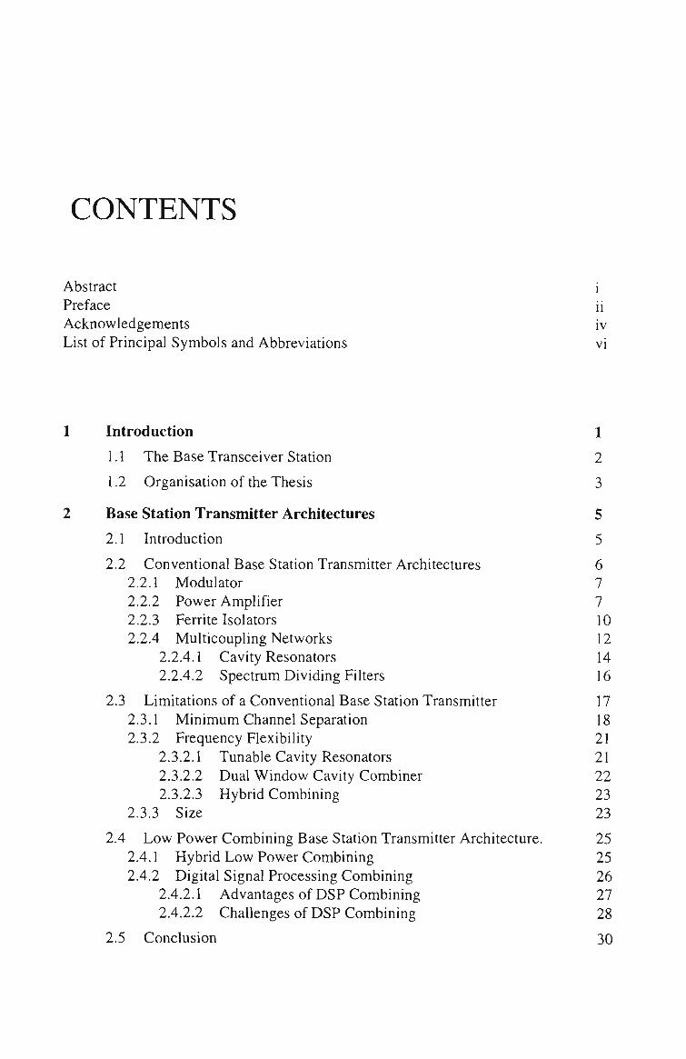
The basic elements that make up the architecture are a modulator, amplifier, ferrite
isolator, cavity resonator and the spectrum dividing (SD) filter. Figure 2.1 illustrates how
these basic building blocks are combined to make up the transmit path of a base station.
Chapter 2 - Base Station Transmilier Architectures
RF Modulator Power Ferrite Amplifier Isolator
Tunable Critical SD Cavity Resonator Harness Filter
Information \ ^ /
Figure 2.1: Conventional multicoupling base station transmitter architecture.
2.2.1 Modulator
The modulator encodes the source information onto a bandpass signal with a centre
frequency of fj . The generic single modulated channel can be written as:
Sk(t) = ak(t) cos( 27ufkt+ek(t)) (2.1)
where ak(t) is the amplitude modulation, f^ represents the centre frequency of the channel,
and 0jj(t) the phase modulation.
2.2.2 Power Amplifier
The Power AmpHfier (PA) increases the level of the modulated signal whilst limiting the
amount of distortion generated. The distortion allowed is set by the specifications of the
radio system. This specification covers the region of the spectrum within the channel
being amplified, 'in channel', and also the region adjacent to the channel in question, 'out
of channel'.
The effect of 'in channel' distortion will be to degrade the noise margin of the link. This is
very important in low noise margin systems with dense signal constellations, such as
satellite and fixed microwave links, but has littie effect on the performance of mobile
systems that require higher noise margins to overcome fading and interference effects.
Very stringent requirements apply to 'out of channel' distortion in afl wireless systems. If
a given channel is unoccupied, a receiver listening to that channel should not detect a

Chapter 2 - Base Station Transmitter Architectures
signal. 'Out of channels' signals must therefore be tightiy controlled. The specification of
the spectrum resulting from the modulation and amplification is usually given in the form
of a modulation mask. Examples of modulation masks for a trunking radio system.
MPT1327, and a cellular radio system, GSM, are shown in Fig. 2.2(a) and Fig. 2.2(b).
dBm i
45(47)
Adjacent Channel
6.25 18.75 Offset frequency from carrier(kHz)
Figure 2.2(a): MPT1327 modulation mask for 12.5 kHz channel spacing and 50 W (47 dBm) average output power. The measurement bandwidth is 8.5 kHz (45 dBm) [11].
Note that the modulation mask is most important in the region of the carrier. The
multicoupling network will have little or no control in this region. The primary role of the
mask is then to specify the allowable Adjacent Channel Interference (ACI). The vertical
axis on Fig. 2.2(a) shows the total power level of the channel written in the parenthesis,
whilst the other value is derived from the fact that the measurement filter is specified as
having 8.5 kHz bandwidth. Consequentiy, if we assume that the whole channel is equally
activated, only a proportion (8.5/12.5) of the actual power will be measured using this
filter.
The ACI specification for the trunked radio system is very stringent, 55 dBc from Fig.
2.2(a). This is due to the near-far^ problem where the physical location of each base
station is uncontrolled and where higher power levels are used to broadcast signals across
large areas (compared to cellular systems).
1. "Ilie adjacent channel interference refers to "that part of the total power output of a transmitter under defined conditions of modulation, which falls within the specified passband centred on the nominal frequency of that of the adjacent channels. This power is the sum of the mean power produced by the modulation, hum and noise of the transmitter" [11] 2. The near far problem is simply due to geographical location of the mobile user. If a user is close to the base station and the base station is transmitting a signal to another mobile some distance away (i.e. high power levels) then the situation could arise whereby the spurious signals generated would be of a sufficient level to open the mute of another mobile hstening at a completely different frequency (or system).

Chapter 2 - Base Station Transmitter Architectures 9
Cellular systems. Fig. 2.2(b), allow for a weaker ACI specification of 30 dBc. primarily
due to the controlled nature of their operation. That is, blocks of frequency are allocated to
a specific system, and the use of frequency planning means that adjacent channels are not
transmitted concurrently in the same basestation (cell). Neighbouring channels (2 or more
channels from the carrier centre frequency) are well protected. For these channels the
specification becomes between -60 dBc and -70 dBc.
Different power classes of transmitters are also highlighted in Fig. 2.2(b). GSM specifies 8
classes ranging from TRX 1 (55 dBm) through to TRX8 (34 dBm). This accounts for
different cell sizes, ranging from large cells (TRX 1) to small cells (TRX 5) and down to
micro cells (TRX 8). The base station can also utilise downlink RF power control. This
consists of 15 power steps in 2 dB increments (30 dB), and has the effect of incrementally
moving the mask through the shaded area as shown in Fig. 2.2(b). The measurement
bandwidth for GSM is specified as 30 kHz and power levels using this bandwidth are
shown prior to the parenthesis.
dBm
46.8(55)
34.8(43)
25.8(34)
4.8(13)
TRX1
TRX5 1 \
TRX 8 ' \ \
\ \ ^
1^ ' ^
i "> i
1 ACI H 30 dBc
1
L 1
k
70 dB
r
1 x ^ ""- --- * ^ i « - "
Channel 1 ^?J^^®"! 1 Neighbouring channels Channel ^
' „ ^ Power Control
Range
^ • 100 200 400 600 Offset frequency
from carrier (kHz)
Figure 2.2(b): GSM modulation masks for three transmitter power output classes; TRX 1 -320W (55 dBm), TRX 5-20W (43 dBm), TRX 8-2.5W (34 dBm). The measurement bandwidth is 30 kHz 19].

Chapter 2 - Base Station Transmitter Architectures 10
2.2.3 Ferrite Isolators
Reverse leakage can allow signal power from transmitters on the same combining
network, or signal power directly received from the transmitting antenna, to enter the
output of another channel's power amphfier. The mixing of the wanted and reverse
interference signals in the power amplifier will generate unwanted InterModulation (IM)
products. A vital component in the protection of the power amplifier from the reverse
interferer is the unidirectional characteristic of the ferrite isolator.
Carrier @ f Output Signal
Mini Ccts Amp ZHL-42 Gamp = 30dB
(a)
Reverse Interferer @ f|
(PREV)
^amp Pc
P|M3 i L "reflect
i L
2fc-fi tc fi
(b)
P|M3 t ,
2frfc
-35 -30 -25 -20 -15 -10 Reverse Interferer Signal (dBm)
(C)
Figure 2.3: (a) Reverse interferer arriving at the output of the amplifier and mixing with the carrier to create an output spectrum consisting of IM products, (b) Spectrum of the amplifiers output signal (c) Reverse interferer (P^Ey) plotted against the dominant third order intermodulation product (PJMS)- Class A amplifier operated at its 1 dB compression point, G^^p.P^ =30 dBm.
The ferrite isolator attenuates the amplified signal, travelling in the forward direction, by a
nominal amount (-0.5 dB), whilst the interfering signal, travelling in the reverse direction,
is significantiy attenuated (-25-50 dB [14]). The amount isolation is related directiy to the
intermodulation attenuation specification, which is specified as 70 dBc for both the GSM
and MPT1327 radio systems.
.3. Intermodulation Attenuation "is a measure of the capability of the transmitter to inhibit the generation of signals in its non-linear elements, caused by the presence of the carrier and an interfering signal reaching the transmitter....." [11].

Chapter 2 - Base Station Transmitter Architectures 11
Calculation of the exact amount of isolation requires knowledge of the relationship
between the return interfering signal level and the resulting intermodulation product level
at the output of the amplifier. Fig. 2.3(a) illustrates the situation more precisely assuming
that the amplifier has a dominant third order characteristic. The amplifier's output signal.
Fig. 2.3(b), consists of a wanted carrier P^, amplified by the gain factor G^ p, an interferer
^reflect' which is directly related to the output reflection coefficient of the amplifier, and the
third order products PJMS^ caused through the mixing of these two signals.
The relationship between the reverse interferer, PREV' ^^'^ ' he dominant third order
intermodulation product, PIMS. was measured for a 'Mini Circuits' class A amplifier with
a rated output power of 30 dBm. This is plotted in Fig. 2.3(c) and it shows that the
relationship can be accurately written as:
PlM3=PREV-18dB (2.2)
Thus to achieve an intermodulation specification of 70 dBc (-40 dBm), the reverse
travelling signal incident on the amplifier must be no larger than -22 dBm.
There are two possible sources of interfering signals: those that come from transmitters on
the same combining network, and those directiy received from the transmitting antenna.
For the transmitters on the same combining network, the amount of reverse power arriving
at the transmitter in question is:
PREV = PC + G^p - TX-TXi,,i,^i,„ dBm (2.3)
where the transmitter to transmitter isolation, TX-TXjsoiation' is giyen by the following
formula [14]:
TX-TXisoiation - I^isolator + ^^cavity "*" ^cavity "*• ^isolator "•• cable + " dB (2.4)
where ILisojatop ILcavity = the insertion loss of tiie isolator and cavity, Lcabie= cable losses
^ d lisoiaton cavity = isolation of the ferrite isolator and cavity filter. Given that the carrier
input power is 0 dBm and tiie gain is 30 dB, tiien from Eqn. (2.3) the amount of TX-
TXisoiation required is 52 dB.
Similarly, for signals arriving from the antenna, the amount of reverse power arriving at
the transmitter is:

Chapter 2 - Base Station Transmitter Architectures 12
PREV = Pant-lm " ^^^T-TXisoiation (2-5)
where Pant-int is the interference power received at the antenna and the amount of antenna
to transmitter isolation is given by:
AN 1-1XjjQi jjQjj = Icavity "*" isolator "•" feeder " Lcable ^^ (2.6)
where Lfee gj. = the loss of the feeder. Given that the typical test interferer power received
at the antenna [11], Pgnt-int' is -30 dBc (0 dBm), the amount of ANT-TXisojation calculated
from Eqn. (2.5) is 22 dB, significantly lower than the required TX-TXisoi tion-
The amount of TX-TXjsoiation required for the GSM or MPT1327 (same intermodulation
attenuation specification) multichannel systems is therefore determined from a
neighbouring transmitter on the same combining network. The value, 52 dB, calculated is
somewhat small compared to the 70-80 dB of TX-TXisoi jjojj quoted as a typical
requirement [14]. The difference can be attributed to the use of higher power amphfiers
with class C output stages and a more stringent intermodulation specification.
For the class C amplifier the dominant intermodulation product is typically only 6 dB
smaller than the reverse interference signal. Eqn. (2.2) is subsequentiy modified for a class
C amphfier such that the amount of TX-TX isolation required is 64 dB. This value will be
further increased for a more stringent intermodulation specification such as that defined
for the maximum spurious level (this is discussed Section 2.2.4.2).
The ferrite isolator is a very important device in the conventional base station architecture
because it is used to provide a significant proportion of the required 70-80 dB of TX-TX
isolation. Only small quantities of isolation are contributed by the other components of the
TX-TX isolation equation, Eqn. (2.4).
2.2.4 Multicoupling Networks
The multicoupling network combines die individual transmitters onto a single antenna. It
consists of high Q cavity resonators coupled togetiier with a critical harness. Fig. 2.4(b).
The cavity resonators are typically two pole bandpass filters which perform the role of
reducing intermodulation products, out of band transmitter noise and spurious products
from the transmitter section. They also provide some isolation between adjacent channels.
Fig. 2.4(a), but this is less than the contribution from the ferrite isolators.
Chapter 2 - Base Station Transmitter Architectures 13
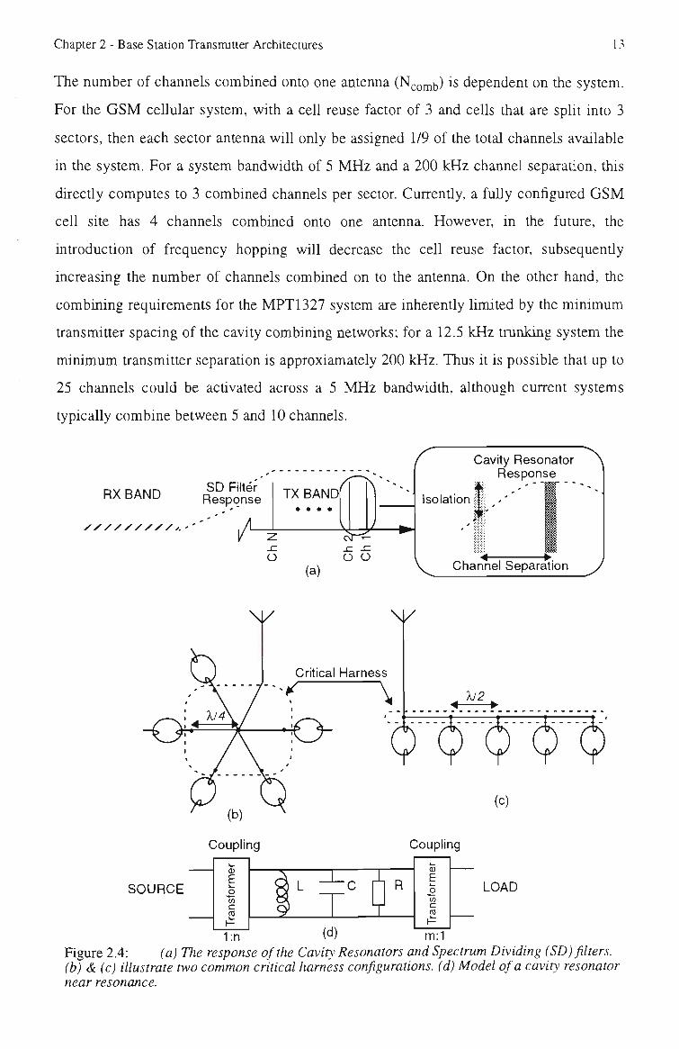
The number of channels combined onto one antenna (N^omb) is dependent on the system.
For the GSM cellular system, with a cell reuse factor of 3 and cells that are split into 3
sectors, then each sector antenna will only be assigned 1/9 of the total channels available
in the system. For a system bandwidth of 5 MHz and a 200 kHz channel separation, this
directly computes to 3 combined channels per sector. Currentiy, a fuUy configured GSM
cell site has 4 channels combined onto one anteima. However, in the future, the
introduction of frequency hopping will decrease the cell reuse factor, subsequentiy
increasing the number of channels combined on to the antenna. On the other hand, the
combining requirements for the MPT1327 system are inherently limited by the minimum
transmitter spacing of the cavity combining networks; for a 12.5 kHz trunking system the
minimum transmitter separation is approxiamately 200 kHz. Thus it is possible that up to
25 channels could be activated across a 5 MHz bandwidth, although current systems
typically combine between 5 and 10 channels.
RX BAND
/ • • • • • / / / > .
SD Filter Response
Cavity Resonator Response
Isolation
Channel Separation
. e i ^
(c)
SOURCE
Coupling
to
(d)
Coupling
I
£
in
c CO
LOAD
1:n W m:1 Figure 2.4: (a) The response of the Cavity Resonators and Spectrum Dividing (SD) filters, (b) & (c) illustrate two common critical harness configurations, (d) Model of a cavity resonator near resonance.

Chapter 2 - Base Station Transmitter Architectures 14
Once combined, and as a final measure to ensure that no interference problems will exist,
the signal passes through another cavity resonator covering the total transmitter
bandwidth. This resonator is used to reduce the transmitter's noise floor (consisting of
broadband noise and spurious products [2]) so that there will be no interaction with other
systems or nearby receivers, which may or may not be connected to the same antenna.
They are commonly referred to as Spectrum Dividing (SD) filters since they isolate
different segments of the spectrum (as shown in Fig. 2.4(a)).
2.2.4.1 Cavity Resonators
As depicted in Fig. 2.1, each amphfied channel is fed into a cavity resonator which is
manually tuned through the means of a tuning stub or screw. The output of each cavity
filter is then coupled into a single output through a critical harness. The critical harness
acts as an impedance transformer, so that the cavity only loads the antenna when resonant.
The behaviour of a cavity resonator is analogous to that of a parallel resonant circuit. Fig.
2.4(d), in the vicinity of resonance, with very high Q values (high selectivity) and low
insertion loss. Coupling into and out of the cavity is modelled as an ideal transformer. At
resonance both the source and load see an impedance that is dependent on the couphng
coefficient into and out of the cavity. It will not be necessarily matched to the source or
load impedances.
The transfer function, H^^^^^yiAf), of the resonator can be approximately modelled near
resonance as:
I H,avity(Af) I = 10 log (1+ (2.Af / BWeavity) ) dB (2.7)
where Af is the offset from the centre frequency, f , and BWcavity is the 3 dB bandwidth of
the cavity. The bandpass response will suppress the IM products, broadband noise and
spurious products, but it is not selective enough to affect the responses in the adjacent
channel or neighbouring channels (as mentioned in Section 2.2.2).
The selectivity of the resonator is directiy related to the loaded Q, QL, of the cavity:
Q L = fc / BWeavity (2-8)
QL must be a large value to obtain sufficient selectivity at UHF frequencies, i.e. for

Chapter 2 - Base Station Transmitter Architectures 15
BWcavity = 600 kHz @ 900 MHz for GSM, QL= 1500. Given that tiie insertion loss of tiie
cavity is approximately (see Appendix A.1):
IL^avity = -20 log (1- Q L / Qo) dB (2.9)
The unloaded Q (Q^) must be sigiuficantiy greater than QL- To keep the insertion loss
lower than 1 dB, Q^ must be at least a factor of 8.2 greater than QL- The design of cavities
is therefore based around attaining large values of QQ. QQ is fundamentally defined as:
Qo = 27t:f . energy stored / power dissipated (2.10)
The volume and the surface area are the mechanisms that store and dissipate energy
respectively. Therefore, the dimensions of the cavity, the use of high quahty materials
(such as silver or copper) and the use of advanced fabrication techniques [15] are
important parameters to achieve large QQ values. As a result, high quality cavities are
expensive, voluminous and heavy.
In the UHF band, the most common kind of cavity is the quarter wavelength coaxial
cavity, operating in TEM mode [3]. These cavities achieve good temperature stability,
high unloaded Q (QQ) values of between 5000 - 10,000 and are relatively compact.
At lower radio frequencies i.e. the VHF band, where the physical size of a quarter
wavelength cavity becomes large, electrically short coaxial cavities, helical resonators and
lumped LC circuits (although these are only practical at the lower end of the VHF
spectrum) become favourable. Helical resonators usually provide Q^ factors of up to 1000.
They can also be used at higher frequencies where they usually perform as wideband
spectrum dividing filters.
More recentiy, high temperamre (70K-100K) superconductor technology has been
developed for cavity filter applications. The surface resistance of such a resonator is a
factor of a thousand times smaller than copper. This translates into Qo values of 40,000 or
more (low insertion loss). The QL value is correspondingly higher (high selectivity) and
the physical size is about one-sixth of copper cavity filters[12]. However, the cost and the
need for a complex cooling system are sufficient obstacles to its universal use in the short
term at least.
Chapter 2 - Base Station Transmitter Architectures 16
2.2.4.2 Spectrum Dividing Filters
The spectrum dividing filter follows the physical channel combination stage. It serves to
attenuate broadband noise and spurious emissions generated by all the prior processes.
Spurious emissions are "emissions at frequencies other than those of the carrier and
sidebands associated with normal modulation" [11]. They are usually specified as an
absolute power level (nominally 0.25uW) measured in a certain measurement bandwidth,
and are a more stringent requirement than either the spectrum mask or intermodulation
attenuation specifications. Additionally, spurious levels are specified at large frequency
offsets from the carrier, as depicted in Fig. 2.5(a).
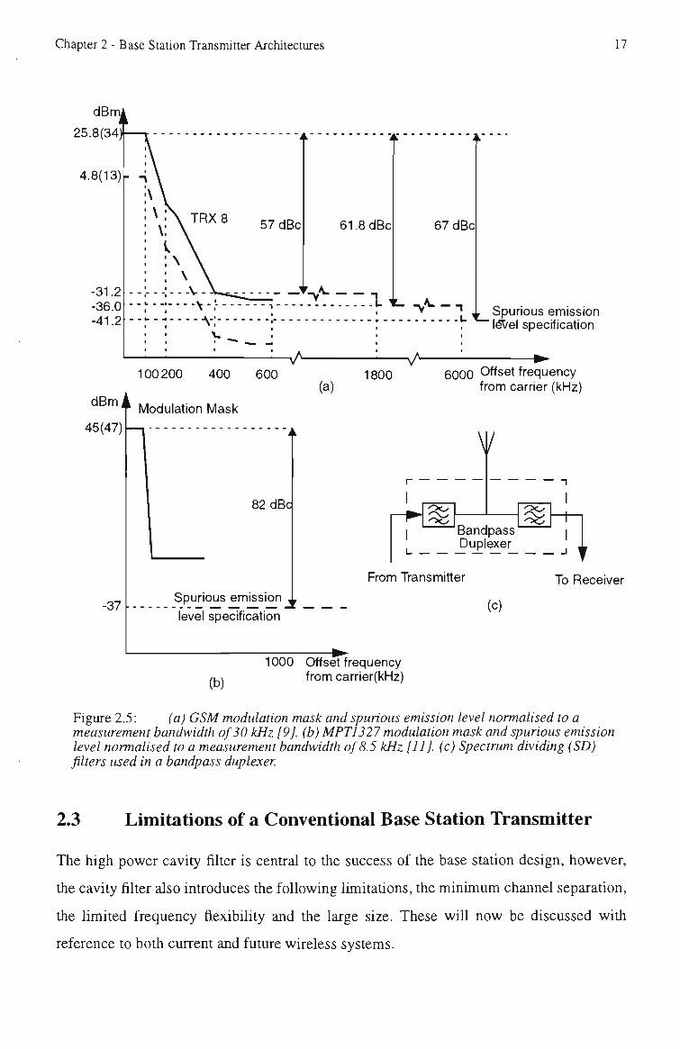
Both Figs. 2.5(a) and (b) are normahsed to a measurement bandwidth, 30 kHz and 8.5 kHz
for GSM and MPT1327 systems respectively. The power is written with respect to the
measurement bandwidth, whilst the power figure given in the parenthesis indicates the
total output power of the channel. Note that the spurious emission level specification takes
precedence over the other specifications. For example, if power control was implemented
for GSM, the lowest level for which the 8* class transmitter (TRX 8) could take would be
4.8(13) dBm. Interference into neighbouring channels should be below -55.2(-47) dBm as
defined by the modulation mask, Fig. 2.5(a), a level substantially below that of the
specified spurious emission level, -41.2 dBm. It is in this situation that the less stringent
spurious emission specification would apply.
The spurious emission level specification sets the transmitter's out of band noise floor
which permits the operation of co-sited receivers without degradation when the
transmitters are turned on. This is particularly important when the transmitter and receiver
are duplexed to the same antenna, as shown in Fig. 2.5(c). The bandpass duplexer achieves
isolation between the receive and transmit paths through the use of bandpass (SD) filters
so tiiat the transmit energy will not desensitise the receiver. A typical requirement in the
transmit path would be for 1 dB insertion loss and 60 dB of isolation [3]. Both coaxial
cavity or helical resonators are used as SD filters.
Chapter 2 - Base Station Transmitter Architectures 17
dBmA
25.8(34
4.8(13).
67 dBc
dBmi
45(47)
-37
100200 400
Modulation Mask
600 (a)
1800
Spurious emission • ISVel specification
6000 Offset frequency from carrier (kHz)
82 dBc
Spurious emission ,^ level specification
V
Bandpass Duplexer
From Transmitter
I
To Receiver
(c)
1000 Offset frequency /u\ from carrier(kHz)
Figure 2.5: (a) GSM modulation mask and spurious emission level normalised to a measurement bandwidth of 30 kHz [9]. (b) MPT1327 modulation mask and spurious emission level normalised to a measurement bandwidth of 8.5 kHz [11]. (c) Spectrum dividing (SD) filters used in a bandpass duplexer.
2.3 Limitations of a Conventional Base Station Transmitter
The high power cavity filter is central to the success of the base station design, however,
the cavity filter also introduces the following limitations, the minimum channel separation,
the limited frequency flexibility and the large size. These will now be discussed with
reference to both current and future wireless systems.
Chapter 2 - Base Station Transmitter Architectures 18
2.3.1 Minimum Chamiel Separation
Future wireless systems have requirements that are based around frequency agihty.
frequency hopping and dynanuc channel allocation. Many more channels will therefore
have to be available for transmission, although not necessarily all at the same time. The
nature of cavity resonators place fundamental restrictions on the minimum channel
separation, which limits the number of channels that can be combined onto a single
antenna. As the channel spacing between the cavities is reduced the insertion (power) loss
increases and the isolation between adjacent transmitters (TX-TXisoiation) decreases.
As the channel spacing is reduced, the isolation between transmitters will decrease
assuming that the cavity is operating at a fixed QL- Ferrite isolators can be used to
compensate for the lost isolation however, it is the problem of increasing insertion loss due
to cavity loading of closely spaced transmitters that is more serious.
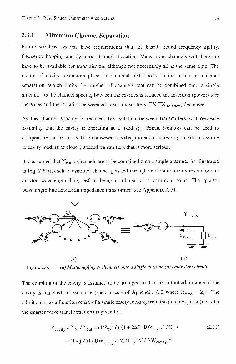
It is assumed that Ncomb channels are to be combined onto a single antenna. As illustrated
in Fig. 2.6(a), each transmitted channel gets fed through an isolator, cavity resonator and
quarter wavelength line, before being combined at a common point. The quarter
wavelength line acts as an impedance transformer (see Appendix A.3).
(a) (b)
Figure 2.6: (a) Multicoupling N channels onto a single antenna (b) equivalent circuit
The couphng of the cavity is assumed to be arranged so that the output admittance of the
cavity is matched at resonance (special case of Appendix A.2 where RRES = Zo). The
admittance, as a function of Af, of a single cavity looking from the junction point (i.e. after
the quarter wave transformation) is given by:
Ycavity = VI Yout = d/Zo)' / ( d + 2Af / B W,,,i,y) IZ^) (2.11)
= (1 - j 2Af / BWeavity) / Zo(l+(2Af / BWeavity)^)
Chapter 2 - Base Station Transmitter Architectures 19
The equivalent circuit has been drawn such that the network is under consideration at the
resonant frequency of one of the cavity resonators. Therefore, the admittance of the
resonant cavity, Y -ayi y, is equal to l/Z^ (from Eqn. (2.11) when Af=0). The antenna is also
assumed to be matched to the characteristic impedance, ZQ, whilst YQ„^ refers to the
equivalent admittance of the remaining (Nj,ojj ,3-l) cavities (Fig. 2.6(b)).
The amount of insertion loss that the channel under consideration undergoes is equal to
the insertion loss of the cavity itself (fL avity as defined in Eqn. (2.8) ) and the insertion
loss caused by the power absorbed in Ygny (see Eqn. (A.22) in Appendix A.4). Total
insertion loss is therefore defined as:
IL = 20 log(l-QL/ Qo) + 10 log( ( l+r)(l+r)*) dB (2.12)
where the reflection coefficient is given by (see Eqn. (A. 17) in Appendix A.4):
r =-Yeq, / (2Y,+Yeq„) (2.13)
When only one resonant cavity is connected to the antenna, Ygqy = 0 and the total insertion
loss is given by that of the cavity itself. The effect of adding more and more cavities to the
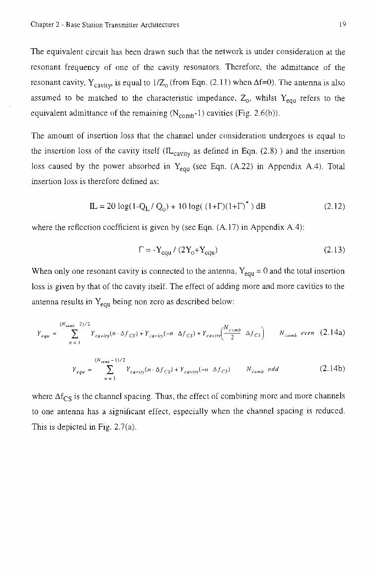
antenna results in Y^^u being non zero as described below:
(W„„,-2)/2
ri= 1
Ye,u = I Yca.ayi" ' ^fcs) + >'c.v,,v(-" ' ^f Cs) + >'cav,;J " f ^ ' ^fcs] ^c.,„fc ^ ^ ^ ^ (2- 14a)
Ye,u = I Yca.i.yi'^ ' ^fcs) + Yca.Uyi'" ^f Cs) ^comb odd (2.14b)
« = 1
where Af^g is the channel spacing. Thus, the effect of combining more and more channels
to one antenna has a significant effect, especially when the channel spacing is reduced.
This is depicted in Fig. 2.7(a).
Chapter 2 - Base Station Transmitter Architectures 20
100 200 300 400 500 600 700 BOO 600 1000 NormaIis.d Chann«l Spacing {KHz)
! i 2 - Tl'-eys
j ^ ^ ' * :
IL:
. ^ "l-cavity
" •
1500 Load«dQ
(a) (b) Figure 2.7: (a) Total insertion loss (IL) for l^comb combined channels. System parameters Qo = 9000, fo = 450 MHz &QL= 1800 (b) Total insertion loss (IL) = IL^ayHy + IL^qu, as a function of the Loaded Q. N=3 and channel spacing = 500 kHz.
In the case when the channels are spaced by large frequencies, Y^^^ will be neghgible (i.e.
open circuit for all resonators at the frequency of consideration) and the additional
insertion loss will also be small. As the channel spacing is reduced, the adjacent cavity
circuits will take on finite values of impedance rather than look like open circuits. This
creates a mismatch at the junction causing both reflection of power and power being
absorbed by the loading of the other cavity circuits. The overall effect is that less power
will arrive at the antenna.
As the channel spacing is further reduced the effect is amplified. Immediately adjacent
channels have a more significant effect on Ygqy, and the other neighbouring cavity circuits
also begin to make contributions. Fig. 2.7(a) shows that the insertion loss rises rapidly as
the channel spacing is reduced. The effect is further pronounced as more channels are
combined onto a single antenna.
The coupling into the cavity was assumed for all previous calculations to be fixed for all
cavities i.e. Q L = 1800. In fact, the coupling into and out of the cavity (directly
proportional to the QL) can be changed to minimise the insertion loss at a given channel
spacing. As the coupling into the cavity is reduced, the loaded Q increases and so does the
cavity insertion loss. However, the high loaded Q shrinks the cavity bandwidth and
reduces the loading effect of the other cavities in the combiner. The insertion loss to other
parallel connected cavities is reduced. Fig. 2.7(b) illustrates the trade-off between IL^avity
Chapter 2 - Base Station Transmitter Architectures 21
and ILgqy. The total insertion loss curve results in an optimum setting of coupling (QL =
1500), to achieve a minimum amount of insertion loss.
Although measures can be taken to minimise the insertion loss, the amount of insertion
loss that can be tolerated within a given system will still restrict the minimum channel
spacing. This is a hmitation of the conventional transmitter architecture.
2.3.2 Frequency Flexibility
Frequency agility is the abihty of a system to rapidly and easily change the channel
frequency, it is seen as an integral component in enhancing the capacity of future radio
systems. For example, the technique of frequency hopping requires the transmitter to
change from one carrier frequency to another in some pre-determined hopping pattern.
The GSM radio system specifies 216.68 hops per second [11]. Frequency agility is also
required to cope with the dynamic load changes within a system. Examples of areas which
may experience large load changes are the main arterials during rush hour, and the CBD
during working hours. Future systems will incorporate flexible frequency plans that
require the dynamic allocation (daily, hourly or even instantaneous changes) of channel
frequencies on a continual process.
The conventional base station architecture as discussed in Section 2.2 has very limited
frequency agility due to the manual tuning mechanism. The architecture can be extended
to achieve limited frequency agility, however, through the use of electro-mechanical
tuning resonators and the dual windows approach. This is at the expense of increased
complexity and cost. Replacing the cavity resonators with a hybrid combiner can achieve
unbridled frequency agility but this technique is very expensive in terms of lost signal
power.
2.3.2.1 lYmable Cavity Resonators
Electro-mechanical tuning resonators are used in the case of a system requiring regular re-
calibration or remote re-tuning of the cavity to a new transmit frequency.
The electro-mechanical solution tunes remotely through the use of stepper motors, RF
sensors, feedback loops and microprocessors. This additional complexity increases the
cost and affects the rehability (mainly due to the introduction of mechanical parts). There
Chapter 2 - Base Station Transmitter Architectures 22
are various techniques for the rapid re-tuning of resonators [17]. The tuning range varies
between 0.05% - 1% of the centre frequency with a degradation in unloaded Q value of
around 50%. Although tuning times in the order of microseconds are achievable, electro
mechanical resonators usually take between 0.1 - 10 seconds to tune [4].
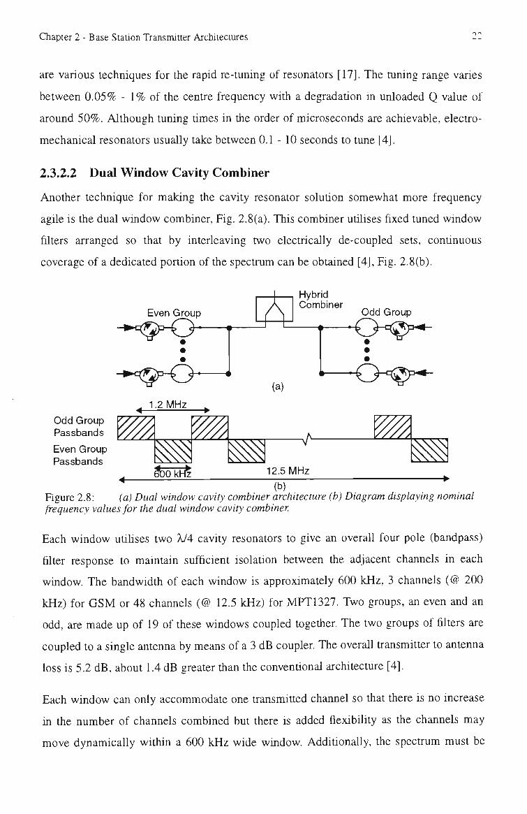
2.3.2.2 Dual Window Cavity Combiner
Another technique for making the cavity resonator solution somewhat more frequency
agile is the dual window combiner. Fig. 2.8(a). This combiner utilises fixed tuned window
filters arranged so that by interleaving two electrically de-coupled sets, continuous
coverage of a dedicated portion of the spectrum can be obtained [4], Fig. 2.8(b).
Even Group
Hybrid Combiner
Odd Group
(a)
1.2 MHz
Odd Group PZ Passbands /////
Even Group Passbands
Vy
^ b
2 V.
N ^
I ^ ^OkHz 12.5 MHz
(b) Figure 2.8: (a) Dual window cavity combiner architecture (b) Diagram displaying nominal frequency values for the dual window cavity combiner
Each window utihses two X/4 cavity resonators to give an overall four pole (bandpass)
filter response to maintain sufficient isolation between the adjacent channels in each
window. The bandwidth of each window is approximately 600 kHz, 3 channels (@ 200
kHz) for GSM or 48 channels (@ 12.5 kHz) for MPT1327. Two groups, an even and an
odd, are made up of 19 of these windows coupled togetiier. The two groups of filters are
coupled to a single antenna by means of a 3 dB coupler. The overall transmitter to antenna
loss is 5.2 dB, about 1.4 dB greater tiian the conventional architecture [4].
Each window can only accommodate one transmitted channel so that there is no increase
in the number of channels combined but there is added flexibility as the channels may
move dynamically within a 600 kHz wide window. Additionally, the spectrum must be

Chapter 2 - Base Station Transmitter Architectures 23
continuous, making it more suitable for cellular systems than for other radio systems
where the spectrum is not allocated in a dedicated block.
2.3.2.3 Hybrid Combining
A technique of combining very closely spaced transmitters (i.e. less than 100 kHz), is
performed through the use of a high power hybrid combiner. Fig. 2.9. There are many
different hybrid topologies [8] that can adequately perform the combining process.
However, they will all exhibit an insertion loss that varies depending upon the phase and
amplitude of the input signals [8]. If the signals are uncorrelated, then the theoretical
average insertion loss that each input undergoes is lOlog^oNcomb' where N omb i ^ c
number of signals being combined. Obviously this is very expensive in terms of lost
power, and this constitutes the major disadvantage of hybrid combining.
RF Modulator A ^ S i e r Circulator High Power SD Hybrid Combiner ' ''*®'' v i ^
Information
Figure 2.9: Hybrid Combining Base Station Transmitter Architecture
A significant advantage of hybrid combining over conventional combining is the ability to
combine channels with no restrictions on channel spacing. However, to maintain high
isolation between ports, it is very important to have a well matched output port. With
accurate manufacturing of the hybrid, only 35 dB of isolation is achievable [2] and so
ferrite isolators will still be needed to achieve the required TX-TXjgoiation-
2.3.3 Size
The need to cope with the increase in eqiupment because of the huge demand for wireless
systems in the future makes size a primary goal for afl system components, including the
base stations [13]. Given that base station sites are both a hmited and expensive resource,
tiie efficient use of space is also essential. Over the last decade this has resulted in the
shrinking in size of base stations. For example, in the NMT (Nordic Mobile Telephone)

Chapter 2 - Base Station Transmitter Architectures 24
system, the volume per channel of a base station was reduced by a factor of around 4
between 1985 and 1990 [13]. If forecasts hold true, the volume of base stations must
continue to be considerably reduced so that the number and area of basestation sites do not
expand at the same rate.
The open market approach to wireless communications, adopted worldwide, allows for
new private operators to compete against the established telecommunication operators.
These operators will also require premises for their infrastrucmre. This will place
enormous pressure on sites in urban environments. Small base stations will be highly
desired to keep site costs minimal.
Future wireless systems, especially cellular, also make provisions for hierarchical cell
structures that consist of very small cell sizes, micro and pico. An unobtrusive base station
might be located on a lamp post, in a mall, or in the comer of an office. It wifl have a major
aesthetic requirement, which will again most easily be met by small size.
Cavity resonators account for the considerable volume in the conventional base station
transmitter. Typically they take up around 30% of the rack space. As highlighted in Table
2.1, the volume and weight of a cavity resonators is very significant. The removal of cavity
filters from the architecture will result is considerable size and weight reductions.
Table 2.1: Nominal Cavity Resonator Data [19]
Frequency Band (MHz)
420-512
900 MHz
Resonator Type
X/4 coaxial
X/4 coaxial
Volume (m ) / Channel
0.05
0.01
Weight / channel
6 Kg
4 Kg
Chapter 2 - Base Station Transmitter Architectures 25
2.4 Low Power Combining Base Station Transmitter Architecture.
By using a low power combining scheme, followed by a high power, hnear and wideband
amphfier a significant improvement can be achieved in terms of flexibihty and
performance. The concept essentially involves the removal of the voluminous and
inflexible cavity resonators, and a subsequent rearrangement in the amplification and
combining processes. The low power combining can occur in either an analogue or digital
environment, giving rise to two architectures, hybrid combining or digital signal
processing combining.
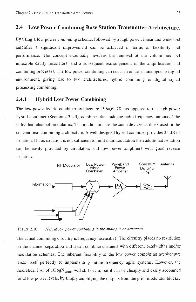
2.4.1 Hybrid Low Power Combining
The low power hybrid combiner architecmre [5,6a,6b,20], as opposed to the high power
hybrid combiner (Section 2.3.2.3), combines the analogue radio frequency outputs of the
individual channel modulators. The modulators are the same devices as those used in the
conventional combining architecture. A well designed hybrid combiner provides 35 dB of
isolation. If this isolation is not sufficient to limit intermodulation then additional isolation
can be easily provided by circulators and low power amphfiers with good reverse
isolation.
RF Modulator Low Power Hybrid
Combiner
Wideband Power
Amplifier
Spectrum Antenna Dividing
Filter
Information P A > — • - •
Figure 2.10: Hybrid low power combining in the analogue environment.
The actual combining circuitry is frequency insensitive. The circuitry places no restriction
on the channel separation and it can combine channels with different bandwidths and/or
modulation schemes. The inherent flexibility of the low power combining architecture
lends itself perfectiy to implementing future frequency agile systems. However, the
tiieoretical loss of lOlogN^ oj b ^iU still occur, but it can be cheaply and easily accounted
for at low power levels, by simply amplifying the outputs from the prior modulator blocks.

Chapter 2 - Base Station Transmitter Architectures 26
The wideband amplifier has been the major technological obstacle. It has low DC-RF
efficiency, high cost and limited total output power. The most important problem,
however, is that the necessary linearity specifications are hard to meet To achieve
sufficient linearity from the amplifier, the technique of 'back-off has traditionally been
used [5,6a,6b]. However, in a multichannel situation, the DC-RF efficiency is
consequently very low, and a large back-off will mean that the amplifier becomes
expensive mainly due to the large amount of over-rating required. Linearisation techniques
are seen as a means of improving the DC-RF efficiency and lowering the device power
rating. Extensive research has been carried out into the linearisation of wideband
amphfiers, utilising techniques such as predistortion and feedforward. Commercial
solutions are now becoming available for small cell sizes.
2.4.2 Digital Signal Processing Combining
The combining can also be implemented in a digital signal processor. This further
increases the overall flexibility of the design by incorporating the modulating and
combining tasks together in a common processor under complete software control.
Ultimately the DSP solution would mean a single hardware platform for the
implementation of a generic base station architecture.
Modulator & Combiner Wideband
Upconverter Power Amplifier
Spectrum Antenna Dividing
Filter
Information w w
^ w
Ik ^ W Digital Analogue
Figure 2.11: DSP low power combining in the digital environment.
There is also a considerable saving in hardware. The hybrid combiner requires a separate
synthesiser, local oscillator and upconverter on a per channel basis, whilst the DSP
solution requires this hardware only on a per system basis. The architecture highhghts the
modulation and combination occurring in a DSP environment. Fig. 2.11. Both the
advantages and chaflenges relating to the DSP low power combining architecture will now
be discussed.

Chapter 2 - Base Station Transmitter Architectures 27
2A.1.1 Advantages of DSP Combining
Software Flexibility
The digital signal processor is inherentiy flexible because the functionality is
programmable. That is, the modulation format or channel frequency can be dynamically
changed by selecting a different subroutine or variable. It is technologically feasible to
produce a generic base station for many different radio system standards.
High TX-TX Isolation
The transmitter to transmitter isolation is set by the precision of the DAC and DSP,
because the modulated channels are combined in a DSP environment. It can be easily
controlled by ensuring sufficient precision in both components.
Low Power Loss
Any power loss that occurs after amplification is critical as it increases the effective power
rating of the amplifier. In the conventional architecture, a significant amount of power loss
occurs due to the cavity resonators, isolators, SD filters and cable loss. Combining at low
power levels means that the power loss after amphfication is somewhat smaUer, equal to
that of the SD filter and the cable only.
No Restrictions on the Minimum Channel Separation
The cavity resonators restrict the minimum separation between channels in the
conventional base station transmitter architecture. In the DSP low power combining
architecture no restriction exists and all channels within a given bandwidth can be
combined and transmitted simultaneously. Channels with different bandwidths and/or
modulation schemes can also be combined. The inherent flexibility of the DSP combining
architecture therefore lends itself perfectiy to implementing future frequency agile
systems.
Silicon Integration
Most components leading up to the wideband amphfier, including die DSP, DAC, mixers
and hybrid combiners, can currentiy be implemented in silicon. As with all types of
electronic equipment, significant reductions in size can be made through silicon
integration. Considering that the cavity resonators have also been removed, a major size
reduction in the base station transmitter will result.

Chapter 2 - Base Station Transmitter Architectures 28
Cost of Equipment and Maintenance
Removal of the expensive precision made cavity resonators from the base station
architecture will contribute to a reduction in the cost of equipment. In addition,
maintenance (calibration) and re-tuning of the cavities requires a technician to make a site
visit to mechanically tune the cavities. This process is both time consuming and
expensive, especially if frequency re-planning of the radio system occurs regularly.
2.4.2.2 Challenges of DSP Combining
Multichannel Combining
A number of channels will require both modulation and combination, and this could occur
across a bandwidth of up to 50 MHz. Consequentiy the computation load will be large.
Efficient algorithms for the combining and modulating process are an essential element
for practical implementation in a DSP environment. The output samphng rate of the
digitally produced multichannel signal will also place large demands on the digital signal
processor. Chapter 3 will investigate efficient DSP combining algorithms.
DAC Interface
The high precision and speed requirements of the DAC interface have always been
considered a limitation of the DSP architecture. This is primarily because the high speed
requirements correspond to lower precision commercially available devices.
The performance of the DAC is measured by the Signal to Noise Ratio (SNR) and the
Spurious Free Dynamic Range (SFDR), both of which are degraded by static and dynamic
errors of the device. These errors will generate harmonic and IM products that will fall
into neighbouring channels, and can exceed the stringent spurious emission specification.
Fig. 2.5(a) & (b). A technique for improving the SFDR will be introduced in Chapters 5
and 6.
Frequency Conversion to RF
Upconversion to RF will incorporate either quadrature or heterodyne techniques, or a
combination of both.
Quadrature upconverters have a well known source of error, namely ampHtude and phase
imbalance between the In Phase (I) and Quadrature (Q) paths [1]. The imbalances result in

Chapter 2 - Base Station Transmitter Architectures 29
undesired sideband signals that will faU into a neighbouring channel. In addition, both
quadrature and heterodyne upconversion stages incorporate mixers, which are nonhnear
devices. Subsequently, the multichannel signal will generate intermodulation components,
or more unwanted spurious responses. The different spurious signals will invariably fall
into neighbouring channels, and therefore must not exceed the spurious emission
specification of the particular system.
Intermodulation caused by mixer nonlinearity can be controlled by incorporating high
intercept point mixers and lowering the input signal level into the mixer. This does not
present any serious technical problems [6b], however the amplitude and phase errors of
analogue quadrature upconverters require correction. A novel compensation circuit will be
introduced in Chapter 4.
Wideband Ultra-Linear Power Amplifier
The wideband power amplifier is a major technical challenge because of the problems of
non-linearity and power output. The nonlinearity of the amplifier will produce
intermodulation components which must not exceed the system specification. From Fig.
2.5(a) (GSM, power class TRX8) tiie spurious emission level must be at least -61.8 dBc
within 6 MHz of the carrier, and from Fig. 2.5(c) the MPT1327 requirement is in the order
of -82 dBc spurious rejection. The spurious rejection must be consistent across a wide
bandwidth; therefore, ultra-linear amplifier behaviour is required. This is technologically
feasible as an amplifier in the 900 MHz cellular band has been reported to suppress third
order products to 70 dBc over a 5 MHz bandwidth [7].
The maximum power output level achieved by wideband, ultra-linear amplifiers also
presents a major technical obstacle. This is aggravated by the fact that the peak power
level of multichannel signals significantly increases the total power rating of the amplifier.
For example, if N omb channels are shnultaneously activated at an average power of P^y,
the total average power of the Ncomb channels is:
Ptav = Ncomb • Pav (2-15)
The actual peak power is significantiy larger than tiiis value. In fact, assuming a worst case
scenario, where all channels peak powers are coherent, tiie Peak Envelope Power (PEP) is
Ncomb times the total average power (Pfav)- For example, witii 4 channels activated, each
Chapter 2 - Base Station Transmitter Architectures 30
having an average channel output of 20 watts (GSM power class TRX5), the PEP is
equivalent to 320 Watts. A good linear amplifier has intermodulation products 30 dB down
at rated power [5] given that the third order distortion is dominant. Therefore to achieve -
72 dBc of spurious rejection, the amplifier must be operated at a backoff of 21 dB. The
rated power of the amphfier required for combining 4 channels would therefore be 40,000
Watts! For the PMR trunking system with more combined channels the situation is even
worse.
A way of decreasing the effective rating of the amplifier is to linearise the amplifier.
Currently commercially available feedforward linearised amplifiers obtain in the order of
60-65 dBc suppression of intermodulation products at up to 25 Watts of total average
power [Microwave Power Devices feedforward amplifier]. For a 4 channel system this
amounts to 6 Watts of average power per channel, matching only the 7* (TRX7) and 8*
(TRX8) power class specifications in the GSM base station transmitter.
It is obvious that high power transmission, using a low power combining architecture is
restricted by the practical size of the ultra-linear amplifier. Current amplifier technology is
capable of meeting only low power outputs, synonymous with small or micro cells.
Therefore, this thesis will consider the GSM TRX8 transmitter specification as an example
of smaller sized cells and the MPT1327 radio system as an example of a larger sized cells.
The wideband amplifier will not be considered any further.
2.5 Conclusion
This chapter has discussed the conventional base station transmitter architecture, central to
which is the cavity resonator. It has been shown that the cavity resonators hmit the
flexibihty and minimum channel separation of the transmitter and they are also very large
and heavy. A low power combining architecture has been introduced to overcome these
hmitations. It rearranges the amplification and combining processes in order to eliminate
tiie requirement for a voluminous and inflexible cavity filter.
Low power combining can occur in the analogue environment through the use of a hybrid
combmer. However, by combining in a digital signal processing environment, a more
flexible solution is possible. The advantages of a DSP combining architecture over the

Chapter 2 - Base Station Transmitter Architectures 31
conventional architecture is the large and easily controlled TX-TXigoiation' 1°^ power loss,
no restriction on the minimum channel separation and the possibihty of silicon integration.
All these factors will result in a smaller, less costiy and more flexible base station
transmitter.
However, there are also a number of challenges presented by the DSP low power
combining architecture. The thesis will concentrate on these design challenges leading up
to but not including the ultra-linear wideband amphfier.
The next chapter will consider both the DSP combining of the channels and the
upconversion of the multichannel signal to RF.

Chapter 3
Multichannel Combining and Upconversion Techniques
3.1 Introduction
This chapter explores the two central issues of the digital signal processing base station
transmitter: the combining of multiple channels and the upconversion of the multichannel
signal to RF.
Section 3.2 defines the relevant parameters of the multichannel RF signal and introduces a
generic architecture for generating the baseband multichannel signal. The architecture is
implemented in a DSP environment and is extremely flexible in terms of channel shaping,
modulation format, power control and frequency allocation. The combining process must
also be computationally efficient. It is shown that the amount of computation is dominated
by the sample rate interpolators and for this reason three efficient interpolation techniques
are investigated.
The remaining sections of the chapter concentrate upon the upconversion of multichannel
signal to RF. This involves digital to analogue conversion and the translation of the
baseband multichannel signal to RF. Section 3.3 investigates the main design issues of
four upconversion techniques:
• digital IF upconversion
• subsampling upconversion
• analogue direct upconversion - lowpass filter reconstruction
• analogue direct upconversion - bandpass filter reconstruction
The Chapter concludes that the two analogue direct upconversion techniques offer a less
complex and a more practical solution than the digital IF techniques. 32

Chapter 3 - Multichannel Combining and Upconversion Techniques 33
3.2 JMultichannel Combining
Multichannel combining involves stacking N modulated channels together into a
Frequency Division Multiplex (FDM) format. An example of a symmetrical stacking
arrangement is shown in Fig. 3.1. The system (or switching) bandwidth, BW^y , is related
to the channel bandwidth, BWc^, and tiie number of channels, Nc^, by:
BW,y3 = Nch X BWch (3.1)
The actual system bandwidth, EWgyg, over which any channel may exist, could be up to 50
MHz. However, this thesis will consider 5 MHz as the system bandwidth, BW^yg, since
this is more representative of the bandwidth allocated to a single operator in Australia (e.g.
Optus, Telecom, Vodafone).
BWsys
/oy iV /kV
Figure 3.1: A multichannel signal centred at a frequency f^.
Figure 3.1 suggests that every channel across the system bandwidth is being combined and
transmitted simultaneously. This is definitely not tiie case, GSM and MPT1327 radio
systems typically only combine up to 4 and 10 channels respectively. However, the need
for more capacity in the future will see radio systems simultaneously transmitting
(combining) more channels.
The multichannel signal as iflustrated in Fig. 3.1 can be written as:
S(t) = Y. «)t(?)cos(w^.r + e^.(0) (3.2) fc = 0
r-Ncomb - 1
= Re k = 0
where the number of combined (or simultaneously activated) channels is denoted by
Ncomb- Th^ multichannel expression can also be rewritten in a number of different ways.

Chapter 3 - Multichannel Combining and Upconversion Techniques 34
For example, the complex baseband signal can be derived by substituting w j.= (wj.-n c +H'C)
into Eqn. (3.2):
S(t) =
fNcomh-'^
J a^(Ocos((w^-^ k = 0
f^comb-^
- X MOsin((w^-
,
w,)f + e^(0) COSVt'^f
)
\
->v^)/ + e^(0) sinw^/ V ^• =
(3.3)
The bracketed terms can be replaced by:
N-l
Xi(t) = Y. «jt(Ocos((w -w )/ + Gjt(r)) ^ = 0
(3.4)
N-\
XQ(t) = ^ a^{t)sini(w^-yvjt + 6^(t)) jt = 0
SO that Eqn. (3.3) can be simply re-written as:
(3.5)
S(t) = xj(t) cos Wet - XQ(t) sin Wct (3.6)
Equations (3.2), (3.3) and (3.6) describe the same multichannel signal transmitted about a
carrier frequency fc- This can be termed a narrowband complex bandpass system if the
bandwidth of the multichannel signal is smaller than the carrier frequency. With no loss of
generality, the multichannel signal can be represented as an equivalent low pass signal or a
complex baseband signal:
R(t)=xi(t)+jXQ(t) (3.7)
The multichannel signal at RF can now be written in the following two forms:
S(t) = IR(t)l cos( Wet + (t)(t)) (3.8)
= Re{R(t)eJ^'^M (3.9)
where the instantaneous amplitude and phase is given by IR(t)l = Jxj(t)^ + XQ(tf , and ())(t) =
-tan"^ ( XQ(t) / Xj(t)) respectively.

Chapter 3 - Multichannel Combining and Upconversion Techniques 35
It is difficult to generate the RF multichannel signal, S(t), due to the high sample rate
requirements. The sample rate requirement can be substantially reduced if the
multichannel complex baseband signal, R(t), is generated in the DSP. Analogue
techniques are then used to translate the signal to RF.
3.2.1 Generation of the Digital Baseband Multichannel Signal
The synthesis of the complex baseband multichannel signal using DSP is shown in Fig.
3.2. The input data for each channel is modulated and frequency translated to the desired
channel location, before being combined with the other channels. The output from the
modulator is in the form of a complex baseband signal, rjj(n), sampled at a much lower
sampling frequency of fg-mod-
;fc( ) = ^i,k^^) + J^q,k^^) (3-10)
= a^{m)e
This signal requires interpolation to the output sampling rate of fs-comb (see appendix B),
before being frequency converted, via digital multiplication, to the desired channel
location (intermediate frequency of fj,). The resultant signal is given by rj jp(m):
/ 271/^. A f 2nf^ \
fi^ipim) =a^(m)cosl-7 m + Q,.{m) \+ ja,^{m)s,\n\- m + 0^(m) J (3.11)
The discrete complex baseband multichannel signal can be written as:
R(m)= X '•A,/M'«) (3.12) k = Q
The output sampling frequency, fs-comb' i selected such that the system bandwidth meets
the Nyquist criteria. Some oversampling is required to reduce the complexity of the
subsequent filtering operations, and it is defined as: OS = fs-comb/BW,y3 (3.13)

Chapter 3 - Multichannel Combining and Upconversion Techniques 36
Baseband Processing •2tfk rr. JrT—^m
Channel
IF Processing
I'•k(m) X rkjF(m)^-R(m)
f, s-comb
4-
(a)
BW,
"'s-comb''^ BWsys ^k f, s-comb' /2
(b) Figure 3.2: (a) Generic architecture (only one channel shown) for generating a complex baseband multichannel signal, R(m). (b) Multichannel complex baseband signal represented in the frequency domain
The multichannel combining technique described and illustrated in Fig 3.2(a) is extremely
flexible. Frequency and power control can be instantaneously apphed at the multiplier and
the channel spectral shaping can be controlled by the interpolating low pass filter, h(m).
However the computational requirements, determined by the complexity of the
interpolation, frequency conversion and summation stages, are very large and optimisation
of these stages is therefore necessary.
The hardware platform places constraints on the optimisation of the computational
requirements. There are two types of hardware platforms: general purpose^ or special
purpose^ digital signal processors. Crochiere and Rabmer [28] present optimal techniques
for general purpose digital signal processors based on minimising the number of
operations per second and the amount of storage (memory) required. Their approach
centres around multistage interpolation, where each stage employs an efficient filter
design, such as a polyphase (Appendix B.l) or a halfband (Appendix B.2) filter. These two
filter designs will be used as a means of approximating the number of operations^ per
second required by a general purpose signal processor.
1. General Purpose -The implementation of algorithms is completed in software, e.g. C40. The main advantage is flexibility. 2. Special Purpxjse - The implementation of algorithms is completed in hardware i.e. ASIC's. FPGA's. The main advantage is the higher computation capabilities.

Chapter 3 - Multichannel Combining and Upconversion Techniques 37
Special purpose digital signal processors (hardware) can use many other optimisation
techniques. For example, the careful choice of filter coefficients [40] or the use of
multiplier-less filters [39] will lower the hardware requirements. The benefits of these
techniques do not necessarily apply to a general purpose digital signal processor, and they
will not be considered in this thesis.
3.2.2 Multichannel Combining Applications
3.2.2.1 A Trunking Radio System - MPT1327
A Private Mobile Radio (PMR) trunking system, such as MPT1327, is an example of an
analogue narrowband wireless system. MPT1327 specifies a channel bandwidth of 12.5
kHz, for frequency modulated speech or data input signals (typically 2.55 kHz deviation).
The modulator is illustrated in Fig. 3.3, and produces a complex baseband signal, ri^(n),
which has a constant amplitude rotating phasor.
A sampling frequency of 12.5 kHz (equal to the channel bandwidth) is sufficient to
represent the FM signal, because the main body of the FM spectrum is contained within
10 kHz' . Cellular systems on the other hand intentionally allow the spectrum to spread
into adjacent channels. This enables a higher data transmission rate, but forces the
complex baseband modulator to operate at a faster sampling rate (fs-mod»BWch).
MPT1327 Complex Baseband Modulator
Audio-
Data-
Signal Conditioning
FFSK encoder
Deviation Limiter
^-mHA Tkln)
Channel Shaping Filter- fcut-off =2-40 kHz
@fs-mod= 12.5kHz
Figure 3.3: MPT1327 Complex Baseband Modulator
PMR wireless systems are also considered to have non-overlapping channels i.e. the
spectrum does not spread across into adjacent channels. The channels are therefore
considered to be well defined segments which are stacked together to form the
3. An operation is classed in terms of a general purpose signal processor as "the amount of work that can be accomplished by a given resource (i.e. a CPU which may include a multiplier, ALU, address multiplexer and internal registers) in a single clock cycle"[35]. For example the add and multiply instructions will take one cycle or operation on most pirocessors. But for a FIR filter implemented using a repeat loop will take {7+(m,ap-l)} cycles or operations to complete (on a C40 [37]). This value will be different for other processors. A C40 operation will be assumed in this thesis. 4. Carlson's rule BWft„= 2*(fd„ia,ion + finput = 2*(2.55+2.4) kHz = 9.9 kHz.

Chapter 3 - Multichannel Combining and Upconversion Techniques 38
multichannel signal. From the modulation mask and maximimi spurious level
specifications. Fig. 2.5, the adjacent channel power must be 82 dB below the maximum
carrier level (82 dBc).
Before combining the channels, the complex baseband modulated signal must be first
mterpolated and frequency translated. Fig. 3.4(a). The amount of computation required to
complete the interpolation, using a single stage polyphase filter, and mititiplication of one
channel is:
Cpoiy(per channel) = {One stage Polyphase Interpolation} + {Multiphcation} (3.14)
- (2 X mtap X fs-mod + + 2 xf3.comb) xlO'^ MOPS-
where m ap is the number of filter taps. The C40^ processor will be used to calculate the
number of operations.
2nfk
X
rkln)
Xq
1
t) 1 -
_ __ ^_ COG m I" Interpolator"^ ^'-"""l
R(m)
f s-mod (a)
s i n i ^ m 's-comb
•s-comb — l- • 'si
82 dB
A. kHz 6.25 12.5 V fs-comb/2^
(b)
Hnterpolato? Interpolato?
Xi,k(n)--t|^J>[h^^}ttH*H^ I II I
2rt(k r — — — -I cos-;—^m Interpolator ''-'•'"'"'
I 11 I I I \
I 11 1 I - - " . oJ^ ^ ^
R(m)
Stage 1 Stage 2
f s-mod
Stage
f, s-comb = ( L i . L 2 . . L j ) . t s-mod
(c) Figure 3.4: (a) Brute force multichannel combining - One stage interpolation and then frequency conversion before the final summation, (b) Specification for the first stage interpolation filter (c) A more efficient multichannel combining technique - Multistage interpolation and then frequency conversion before the final summation.
5. MOPS - Millions of Operations per Second 6. C40 refers to the TMS 320C40 processor, which is capable of 25 MOPS when the processor clock is 50 MHz.

Chapter 3 - Multichannel Combining and Upconversion Techniques 39
The number of taps for the single stage interpolator will be large because the transition
width of the filter is small (2 kHz) compared to the output samphng frequency, as
illustrated in Fig. 3.4(b). A useful approximation for computing the number of taps, m^™,
given a set of specifications [23] (Parks McClellan Technique) is:
f^tap = ( - 2 0 1 o g 5 - 1 3 ) / ,
14.6 • Afj (3.15)
where 5 is equal to the passband and stopband ripple, Afj is the transition region and fg is
the output sampling frequency of the filter. For the MPT1327 radio system. Fig. 3.4(b), the
stopband ripple is equal to 82 dB and the transition bandwidth is 2 kHz. The system
bandwidth, or minimum sampling rate (fs-comb) is assumed to be 5 MHz, resulting in at
least 11,815 taps! The interpolation process can be made more efficient if a multistage
design is employed, Fig. 3.4(c).
It will be assumed that each stage will have an interpolation factor of 2, although other
interpolation factors are possible. Therefore, assuming a system bandwidth of 5 MHz, the
minimum total interpolation factor is 512 i.e. fs.comb - ^^-^ ^^^ x 512 = 6.4 MHz. This
can be achieved by 9 'interpolate by 2' stages. Table 3.1. The efficiency is brought about
by making use of the fact that the transition width increases for each subsequent stage
causing the number of taps per stage to converge to an asymptotic limit. The limit occurs
as the transition width approaches half the sampling frequency; mj™ = 10 (Eqn. (3.15)).
Table 3.1: Multistage interpolation using a cascade of interpolate by 2 stages.
Stage
L
Atyfs
intap
Type
1
2
0.08
60
Poly''
2
2
0.25
19
Half
3
2
0.375
15
Half
4
2
0.438
11
Half
5
2
0.47
11
Half
6
2
0.485
11
Half
7
2
0.493
11
Half
8
2
0.497
11
Half
9
2
0.498
11
Half
a. Poly - Polyphase interpolator b. Half - Halfband interpolator

Chapter 3 - Multichannel Combining and Upconversion Techniques 40
The first stage uses a polyphase interpolation filter because the passband and stopband
frequencies are not symmetrical about a quarter of the output sampling frequency (see
Appendix B.2). However, the remaining stages can use the more efficient half-band filter.
The halfband interpolator is shown to have approximately half the number of operations,
(mtap-t-l)/2, of the polyphase interpolator for a given number of taps (Appendix B).
Additionally, the halfband filter has a lower hardware complexity, making it ideal for
implementation as a special purpose digital signal processor.
Further efficiencies in the multichannel combining algorithm can be gained through the
use of a transmultiplexer algorithm. A transmititiplexer efficiently converts time division
multiplex signals to frequency division multiplex signals. Digital implementation of
transmultiplexors has been subject to a large amount of research and development,
commencing in the 1960's and continuing into the 1980's. A comprehensive survey by
Scheuermann and Cockier [27] presented every type of transmultiplexer proposed as of
June 1981. In this thesis only one transmultiplexer technique, arguably the most
computationally efficient, has been isolated as an example for use as a multichannel
combiner. This technique is called the polyphase Fast Frequency Transform (FFT) filter
bank, illustrated in Fig. 3.5. The efficiency of the algorithm is intuitive if compared to Fig.
3.2(b). The polyphase FFT technique computes the interpolation multiplication and
summation of the channels at the lower sampling rate, fs-mod-
T3 0)
ox|.i(n)
•a
I Xi.2(n)_ « 05
el "BO
|xi.(L._i)(n)_^
CO J:: Q.
c
N Point
Inverse FFT
U, s-mod
Figure 3.5: Polyphase FFT filter Bank. Only showing the In Phase processing path, the Quadrature Phase path is identical.

Chapter 3 - Multichannel Combining and Upconversion Techniques 41
The polyphase FFT filter bank can actually be derived directiy from the single channel
structure described in Fig. 3.2(b). This derivation is completed in detail in reference [28]
and will not be considered here. A few of the important details are:
• The number of channels is made to equal the interpolation rate, L.
The input sampling frequency, fj-mod' sets the channel bandwidth, BWch.
• The original low pass interpolation filter, hj , is decomposed down into L polyphase filters:
qp{n) = h{nL + p) p = 0, 1, ..., L - 1
• The number of channels is made to equal a number that is a power of 2. Therefore, the more efficient FFT as opposed to the discrete fourier transform, can be used.
From previous discussions, an interpolation factor of 512 meets all the above requirements
and the combming sampling frequency of the polyphase FFT algorithm is (512 . 12.5 kHz)
= 6.4 MHz. Given that only 5 MHz of system bandwidth is required, the outer 112 (1.4
MHz) channels will not be used. Using only 400 of the 512 available channels has the
benefit of oversampling the system bandwidth.
The amount of computation power required for the polyphase FFT technique, using the
C40 processor, can be determined using reference [37]. It states that a 512 point inverse
FFT will take 16,067 operations. The number of operations can then be written as:
Cppp = {FFT} + {Polyphase Filter} (3.16)
= 2 X (16,067 . fs-mod + mtap • fs-mod) x 10'^ MOPS
The factor of two in Eqn. (3.16) takes into account both the In Phase and Quadrature
paths.
For each of the techniques discussed, the computation power has been plotted against the
number of combined channels in Fig. 3.6. The following parameters have been used for
tiie calculations: fg-mod = 1 .5 kHz, BW y = 5 MHz and fg-comb = ^.4 MHz.

Chapter 3 - Multichannel Combining and Upconversion Techniques 42
10'
Single Stage Interpolation
20 40 60 60 Number of Combined Channels (Ncomb)
100
Figure 3.6: The number of computations versus the number of channels combined for the MPT 1327 trunking radio system with the following parameters; f^.f^^^j^ = 12.5 kHz, BW^y^ = 5 MHz, f.comb = 6.4 MHz
The Polyphase FFT technique has a constant computation load, regardless of the number
of channels combined, whilst for the other two techniques, the computation load increases
hnearly with the number of combined channels. The polyphase FFT technique requires a
total of 780 MOPS (32 general purpose C40's) of computation whereas the cascaded
halfband interpolator requires 90 MOPS (4 general purpose C40's) per channel.
Figure 3.6 also reveals that the halfband technique is about 4 times more efficient than
single stage interpolation, and is more efficient than the polyphase FFT technique when
the number of channels being combined is less than 8. For the MPT1327 radio system, it is
typical for between 5 and 10 channels to be combined. Either multi-stage interpolation or
the polyphase FFT technique could therefore be used. The polyphase FFT technique
becomes a lot more attractive if we take into consideration future systems, where a larger
number of channels will be combined.
3.2.2.2 A Digital Cellular Radio System - GSM
The GSM radio system specification states that the information bit rate, f^, is 270.833
kbps. To minimise the complexity of the interpolation stage, the output sampling
frequency, fs-comb' is best set to an integer multiple of the input data rate. An overall
interpolation factor of 24 (fs-comb = 24 x f, = 6.5 MHz) will satisfy the above requirement.
The sampling rate is simihar to the previous MPT1327 example, and this will provide a
basis for a fair comparision of computation load between the two systems..
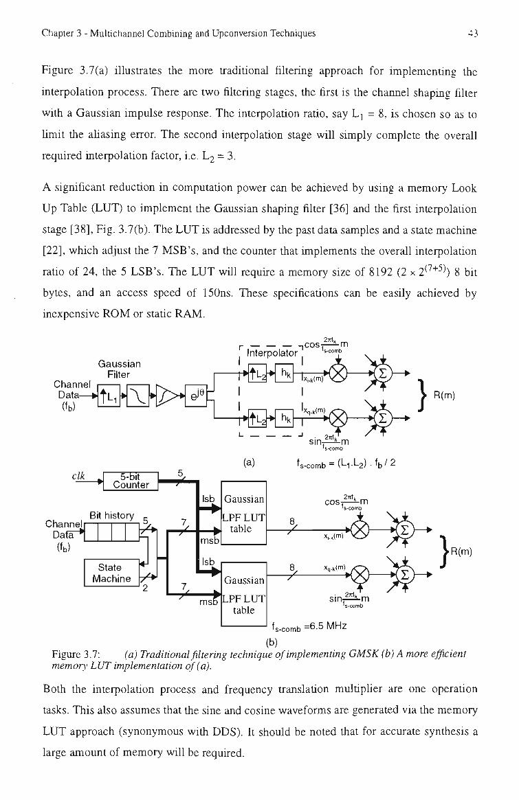
Chapter 3 - Multichannel Combining and Upconversion Techniques 43
Figure 3.7(a) illustrates the more traditional filtering approach for implementing the
interpolation process. There are two filtering stages, the first is the channel shaping filter
with a Gaussian impulse response. The interpolation ratio, say L^ = 8, is chosen so as to
hmit the ahasing error. The second interpolation stage will simply complete the overall
required interpolation factor, i.e. L2 = 3.
A significant reduction in computation power can be achieved by using a memory Look
Up Table (LUT) to implement the Gaussian shaping filter [36] and the first interpolation
stage [38], Fig. 3.7(b). The LUT is addressed by the past data samples and a state machine
[22], which adjust the 7 MSB's, and the counter that implements the overall interpolation
ratio of 24, the 5 LSB's. The LUT wtil requke a memory size of 8192 (2 x 2 " ^ ) 8 bit
bytes, and an access speed of 150ns. These specifications can be easily achieved by
inexpensive ROM or static RAM.
Channel Data—I (fb)
Gaussian Filter
2tfK ^
p — — — -.cos-;—-m Interpolator ^^""^
E J H X H ^ e-" R(m)
sin-i—^m 's-comb
(a) fs-comb = ('-1.1-2) • ^ b / 2
elk 5-bit Counter
Channel Dafa (fb)
Bit history r-
State Machine 7 ^
Isb
msb
Isb
Gaussian
LPF LUT table
2tfk ,v,
cos-;—-m 's-comb
^
^ msi t
Gaussian
ILPFLUT table
"7^
R(m)
sin^—'-m 's-comb
fs-comb =6.5 MHz (b)
Figure 3.7: (a) Traditional filtering technique of implementing GMSK (b) A more efficient memory LUT implementation of (a).
Both the interpolation process and frequency translation multiplier are one operation
tasks. This also assumes that the sine and cosine waveforms are generated via the memory
LUT approach (synonymous with DDS). It should be noted that for accurate synthesis a
large amount of memory will be required.
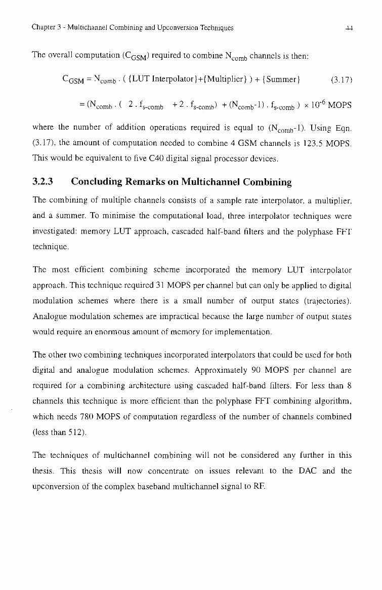
Chapter 3 - Multichannel Combining and Upconversion Techniques 44
The overall computation (C^SM) required to combine Ncomb channels is then:
CGSM = Ncomb • ( {LUT Interpolator}+{Multipher} ) -f {Summer} (3.17)
= (Ncomb • ( 2 . fs.comb + 2 . f comb) + (Ncomb'!) • fs-comb ) ^ 10" MOPS
where the number of addition operations required is equal to (Ncomb" !)• Using Eqn.
(3.17), the amount of computation needed to combine 4 GSM channels is 123.5 MOPS.
This would be equivalent to five C40 digital signal processor devices.
3.2.3 Concluding Remarks on Multichannel Combining
The combining of multiple channels consists of a sample rate interpolator, a multiplier,
and a summer. To minimise the computational load, three interpolator techniques were
investigated: memory LUT approach, cascaded half-band filters and the polyphase FFT
technique.
The most efficient combining scheme incorporated the memory LUT interpolator
approach. This technique required 31 MOPS per channel but can only be applied to digital
modulation schemes where there is a small number of output states (trajectories).
Analogue modulation schemes are impractical because the large number of output states
would require an enormous amount of memory for implementation.
The other two combining techniques incorporated interpolators that could be used for both
digital and analogue modulation schemes. Approximately 90 MOPS per channel are
required for a combining architecture using cascaded half-band filters. For less than 8
channels this technique is more efficient than the polyphase FFT combining algorithm,
which needs 780 MOPS of computation regardless of the number of channels combined
(less than 512).
The techniques of multichannel combining will not be considered any further in this
thesis. This thesis will now concentrate on issues relevant to the DAC and the
upconversion of the complex baseband multichannel signal to RF.
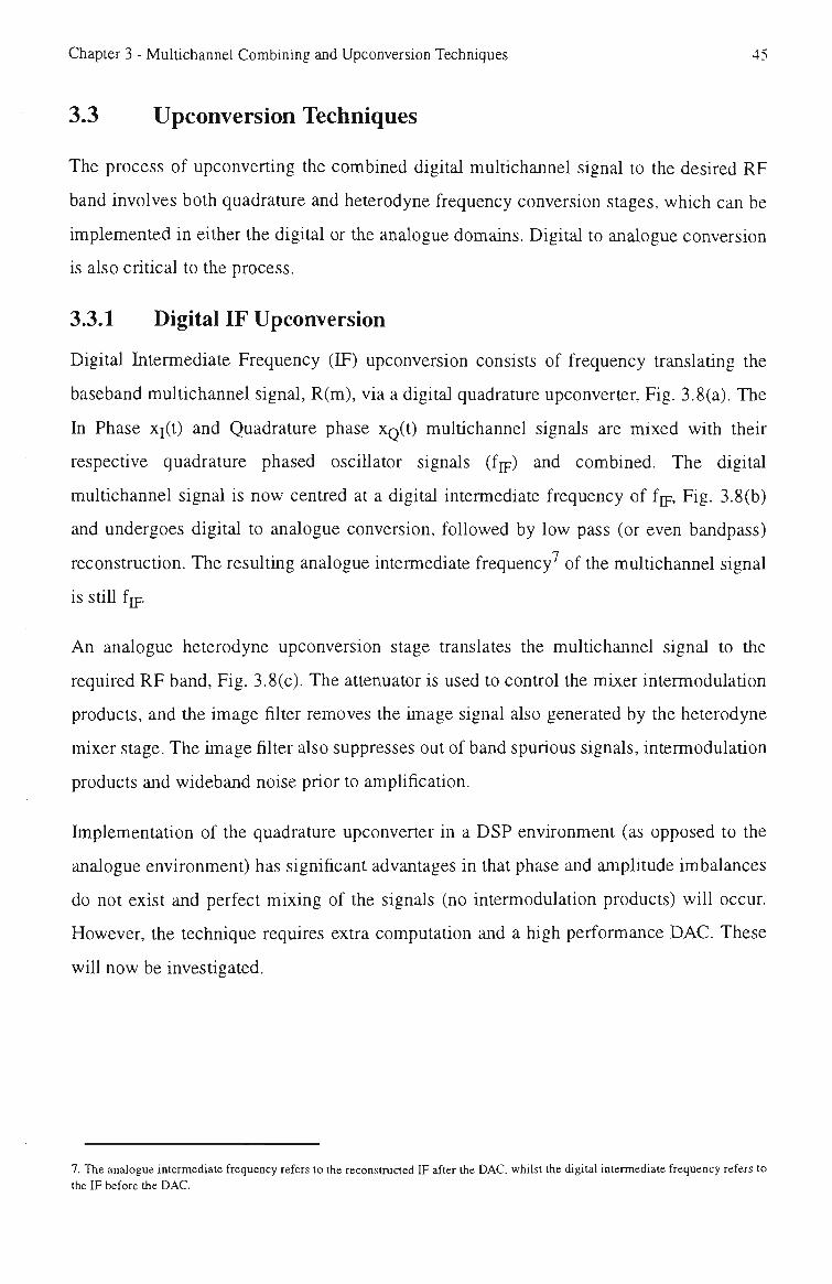
Chapter 3 - Multichannel Combining and Upconversion Techniques 45
3.3 Upconversion Techniques
The process of upconverting the combined digital multichannel signal to the desired RF
band involves both quadrature and heterodyne frequency conversion stages, which can be
implemented in either the digital or the analogue domains. Digital to analogue conversion
is also critical to the process.
3.3.1 Digital IF Upconversion
Digital Intermediate Frequency (IF) upconversion consists of frequency translating the
baseband multichannel signal, R(m), via a digital quadrature upconverter. Fig. 3.8(a). The
In Phase xi(t) and Quadrature phase XQ(t) multichannel signals are mixed with their
respective quadrature phased oscillator signals (fjp) and combined. The digital
multichannel signal is now centred at a digital intermediate frequency of fjp. Fig. 3.8(b)
and undergoes digital to analogue conversion, followed by low pass (or even bandpass)
reconstruction. The resultmg analogue intermediate frequency^ of the multichannel signal
is still fjp.
An analogue heterodyne upconversion stage translates the multichannel signal to the
required RF band. Fig. 3.8(c). The attenuator is used to control the mixer intermodulation
products, and the image filter removes the image signal also generated by the heterodyne
mixer stage. The image filter also suppresses out of band spurious signals, intermodulation
products and wideband noise prior to amplification.
hnplementation of the quadrature upconverter in a DSP environment (as opposed to the
analogue environment) has significant advantages in that phase and amplitude imbalances
do not exist and perfect mixing of the signals (no intermodulation products) will occur.
However, the technique requires extra computation and a high performance DAC. These
will now be investigated.
7. The analogue intermediate frequency refers to the reconstructed IF after the DAC, whilst the digital intermediate frequency refers to the IF before the DAC.

Chapter 3 - Multichannel Combining and Upconversion Techniques 46
[ Quadrature UpconverteP i
X|(m)
R{m)
RF-'IF
DSP I Analogue 1 (a)
BW, sys_
Reconstruction " • - > , Filter - •
(b)
BW
f|F fso/2
sys •^^ Image A ' * ' . Filter
fRF (c)
Figure 3.8: (a) Digital IF upconversion architecture (b) Multichannel signal after DAC (c) Multichannel signal after RF upconversion.
3.3.1.1 Computation Requirements
The frequency of the IF output signal determines the trade-off between analogue
complexity and the computational load. A higher IF requires more computation but
reduces the number of analogue upconversion stages needed to reach the desired RF band.
The additional computation load of digital quadrature upconversion requires careful
consideration.
The baseband multichannel signal, R(m), must be interpolated to the higher output
sampling frequency (fgo) before quadrature mixing and summation, as shown in Figs.
3.9(a) and (b). It is a very similar problem to that discussed in Section 3.2.2. The
calculation of computation will assume a multistage interpolation technique, using
halfband interpolators:
CiF = 2.{stage 1 }.fs.comb + 2.{stage 2}.2.fs.comb + •••• + 2.{stage j}.fso
-I- 2.{multiplier}.fso + {summer}.fso (3.18)

Chapter 3 - Multichannel Combining and Upconversion Techniques 47
The factor of 2 takes into account both I &Q paths. The multipher and summer are 1
operation calculations, where each half-band filter stage takes (mtap+l)/2 operations. The
number of taps is calculated from Eqn. (3.15). Overhead processing, such as trigonometric
generation (via lookup tables) and general program code, is neglected for simplicity. I
r — -^ icosi!ElLFn I Interpolator . u
R(m)
XQ (m) HtL]~^S~r-^^^)-^ •S(t)
f, s-comb (a)
Afj
\ \
BW 's-comb
' ^
'so ~ '- • 's-i
" to i ic_ ' ^
s-comb
Filter atten |20logio8 characteristic
sys (b)
Figure 3.9: (a) Digital signal processing architecture for interpolation and quadrature upconversion. (b) Periodic spectral components of the multichannel signal after interpolation overlaid with tiie filter attenuation characteristics of the interpolation filter.
Additional computational savings can be made by incorporating the multiplier and
summer into the last interpolation stage. Fig. 3.10(a). The savings centre around the
selection of the intermediate frequency to equal a quarter of the output sampling
frequency. The cosine and sine carriers then reduce to:
cos(27rfiFn/fso) = lA-l,0,l,0,-l...&sin(27ufiFn/fso) = 0,1,0,-1,0,1,0... (3.19)
where fjp = f oM
This eliminates the need for generation of the trigonometric functions (although they may
only be in the form of a look-up table). The multiply and addition operations are now
replaced by the multiplexer and negation operations, offering substantial speed and
hardware savmgs. The whole quadrature upconverter (multiphcation and summer) can be
incorporated into the last interpolation operation as shown in Fig 3.10(b) so that the total
amount of computation can be written as:
CiF = 2.{stagel}.fs.comb + 2.{stage2}.2.fs.comb + - - + 2.{stagei-l}.fso/2-h {2 + (stagej)}.fs (3.20)

Chapter 3 - Multichannel Combining and Upconversion Techniques 48
X|(m)
Odd Coefficients
Stage j Interpolator
Centre Coefficient
XQ(m)
Odd Coefficients
Stage] Interpolator
Centre Coefficient
fso/2
X|(m)
XQ(m)
Stage j Interpolator
Centre Coefficient
fso/2
X|(m) — • ! Centre Coefficient
XQ(m) _ Centre Coefficient
fso/2
cosine : 1,0,-1,0,1,0,-1,0....
I ^° ' 'P3f^ |c)_\
_ L J L I
(a)
Odd Coefficients -
> negate
negate
(b)
negate
negate
(c)
> - • S(m)
sine: 0,1,0,-1,0,1,0,-1....
f. 'so
r
- • S(m)
I I
'so
r
T^\ I
->!— I - • S(m)
# J — I
I I
Tso
Figure 3.10: (a) Last halfband interpolator followed by a quadrature upconverter with an intermediate frequency offf/4. (b) Efficient implementation of (a), (c) An even more efficient implementation of (a).
A further simplification can be made by delaying the In Phase path by one sample, as
shown dotted in Fig. 3.10(a). The equivalent circuit is tilustrated in Fig. 3.10(c). The
interpolator, multiplier and summer reduce to two negation operations because the centre
coefficient for a halfband design is equal to 1 (Appendix B.2). The drawback is that the
delay introduces a linear phase shift to the In Phase channel, but not the Quadrature
channel. This establishes a phase imbalance in the quadrature upconverter, which will
generate an unwanted sideband response (Chapter 4 will explore this in detail). The
unwanted sideband can be cancelled by generating the equal and opposite sideband using
tiie original signal, the same technique that is discussed in Chapter 4. This correction

Chapter 3 - Multichannel Combining and Upconversion Techniques 49
scheme will require additional processing. Given that the multichannel wireless
specifications are very stringent, the correction may actually introduce more processing
than what has been saved by introducing the single delay.
The computation power (in MOPS) expressed in Eqn. (3.20) has been plotted for both the
GSM and MPT1327 systems. Fig. 3.11. The system bandwidth for both systems is set to 5
MHz, and the sampling frequency of the combining stage, fs-comb' i taken as 6.5 MHz.
The reason that the GSM system is more efficient than MPT 1327 for any given sampling
frequency is related to the differing maximum spurious level specifications. GSM requires
only -61.8 dBc ahas attenuation, whilst MPT1327 requires -82 dBc.
200 400 600 800 Output Sampling Frequency (IvIHz)
1000
Figure 3.11: Computation power required to interpolate and quadrature upconvert a multichannel signal to an intermediate frequency. Parameters are BW^y^ = 5 MHz. f. comb = 6.5 MHz: MPT1327 - alias attenuation = 82 dBc; GSM - alias attenuation = 61.8 dBc.
From Fig. 3.11, the amount of computation required to upconvert the complex baseband
signal to an intermediate frequency is very large. For example, to achieve an intermediate
frequency of 26 MHz approximately 1100 & 1400 MOPS are required for GSM and
MPT1327 respectively (marked with a ' * ' on Fig. 3.11). This is equivalent to 44 or 56
general purpose digital signal processors which is prohibitive in terms of size, complexity
of hardware, cost, and power consumption.
Some additional reductions could be made by optimising the interpolators or by lowering
the intermediate frequency. Regardless of these savings, implementation using currently
available general purpose digital signal processors is impractical. Special purpose digital
signal processors might be able to handle the processing requirements, by utilizing
optimised filter designs [38-40] and introducing many arithmetic operations in parallel

Chapter 3 - Multichannel Combining and Upconversion Techniques 50
simply by increasing the number of multiphers and adders on the special purpose chip.
Such special purpose chips have recentiy become available. One example is the Harris
HSP50016 Digital Down Converter, which performs the opposite task to that described
here. It achieves an overall decimation factor ranging from 64 to 131072 at a maximum
sampling rate of 75 MSPS. The Harris HSP43216 halfband decimation filter is anotiier
example which downconverts the IF signal to DC (using fso/4 multiphcation) but at a
maximum sampling rate of 90 MSPS.
3.3.1.2 DAC Interface
The high intermediate frequency will place stringent demands on the speed and accuracy
of the DAC interface, both of which affect the output carrier to noise ratio (CNR). This
means that the DAC will hmit the maximum channel power, and it will be the dominant
source of noise, i.e. quantisation noise is greater than any contribution from thermal, shot
or other noise sources.
The following analysis assumes that each transmitted channel is unmodulated with a peak
amphtude of \ , see Eqn. (3.2). The DAC is also assumed to have a Full Scale Range
(FSR) of 2Vnjax- If Ncomb channels are to be combined, then the peak amplitude of each
channel is limited to:
ak = Vmax/Ncomb (3-21)
This assimies the worst case scenario when all the channels are coherent, and the peak
channel voltages add. Allowing for this scenario ensures that the multichannel signal can
not clip. The resulting maximum average power (into one ohm) of each channel is then
defined in terms of the Vr max-
2 , , 2 a,. Vninr
Pav = ^ = ^ (3-22) ^ 2 . NI^^,
Quantisation error will generate noise, which is assumed to be spread evenly across the
Nyquist bandwidth (fso/2) with a tot
defined as the step size of the DAC:
Nyquist bandwidth (fso/2) with a total power into one ohm equal to A /12 [29], where A is
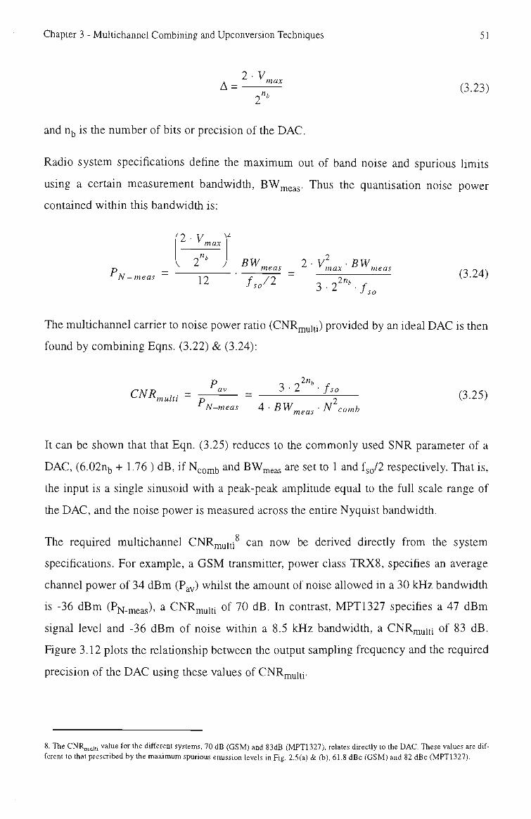
Chapter 3 - Multichannel Combining and Upconversion Techniques 51
2 - y max A = —i^ (3.23)
2
and Uj, is the number of bits or precision of the DAC.
Radio system specifications define the maximum out of band noise and spurious limits
using a certain measurement bandwidth, BW^eas- Thus the quantisation noise power
contained within this bandwidth is:
P — N-meas
(2-V ] max
V 2 J
12 fso/2
2 -V^ • BW max meas
3 - 2 ^ " ' - / „ (3.24)
The multichannel carrier to noise power ratio (CNRjnuiti) provided by an ideal DAC is then
found by combining Eqns. (3.22) & (3.24):
p - -2nfc
CNR^^u, = ; H ^ = ^ ^ T — (3.25) N-meas 4 • BW^,„, • N comb
meas
It can be shown that that Eqn. (3.25) reduces to the commonly used SNR parameter of a
DAC, (6.02nt, + 1.76 ) dB, if Ncomb '^^^ ^^meas ^re set to 1 and fso/2 respectively. That is,
the input is a single sinusoid with a peak-peak amplitude equal to the full scale range of
the DAC, and the noise power is measured across the entire Nyquist bandwidth.
The required multichannel CNRmum^ can now be derived directly from the system
specifications. For example, a GSM transmitter, power class TRX8, specifies an average
channel power of 34 dBm (P^y) whilst the amount of noise allowed in a 30 kHz bandwidth
is -36 dBm (PN-meas)' ^ CNRj um of 70 dB. In contrast, MPT1327 specifies a 47 dBm
signal level and -36 dBm of noise within a 8.5 kHz bandwidth, a CNR^uiti of 83 dB.
Figure 3.12 plots the relationship between the output sampling frequency and the required
precision of the DAC using these values of CNR^uiti-
8. The CNR,„ui,i value for the different systems, 70 dB (GSM) and 83dB (MPT1327), relates directly to the DAC. These values are different to that prescribed by the maximum spurious emission levels in Fig. 2.5(a) & (b), 61.8 dBc (GSM) and 82 dBc (MPT1327).

Chapter 3 - Multichannel Combining and Upconversion Techniques 52
14
its (n
b)
Num
ber o
f I
o
B
c
^ - - ^ P T 1 3 2 7
GSM
•
•
A
^ ^ ^ i
'
10 10 10 Sampling frequency (MHz)
Figure 3.12: The output sampling frequency, f^, versus the number of bits, ny, for GSM and MPT 1327 systems employing the digital IF upconversion technique. GSM (dotted) Ncomb = 4, BW^^^, = 30 kHz and CNR^^ni = 70 dB. MPT1327 (solid) Ncomb= 10, BW^^^, = 8.5 kHz and CNR^ulti = ^^ ^B.
The different CNRj uiti system specification explains the variation between the two curves
(accounting for about 1.5 bits in DAC precision). Additionally, the MPT 1327 system
combines more channels and this wtil account for an additional bit in DAC precision, Eqn.
(3.25). Figure 3.12 also highlights the fact that as the sampling frequency increases the
required precision of the DAC becomes less. On face value this is a very favourable
situation, since commercial high speed DAC's have lower precision. However, can
commercially available DAC's cope with the precision and speed requirements of the
digital IF upconversion technique?
From the survey of DAC's (see Appendix C), the current state of the art is best represented
by the Burr Brown 650, 12 bit @ 500 MHz. This point has been highlighted as a triangle
on Fig 3.12. However, static and dynamic errors cause the real operation of the BB 650 to
exhibit only 9.5 bit precision at 100 MHz sampling frequency (shown as a square on Fig.
3.12). Hence only the GSM system can be converted within the specifications. The
intermediate frequency is also limited to a quarter of the DAC maximum sampling rate
which would be approximately 25 MHz.
It should be highlighted that in the near future the speed and accuracy of commercially
available DAC's should advance considerably. Recently published material suggests that
state of the art DAC techniques are achieving sampling rates in the order of 1 GSample/s
at over 10 bits in precision (see Appendix C). From Fig 3.12, highlighted as a circle, this
would represent enough DAC precision for IP's in the order of 250MHz (assuming fjp =

Chapter 3 - Multichannel Combining and Upconversion Techniques 53
fso/4) to become possible. Regardless of these advances, static and dynamic errors wtil
still compromise DAC performance and need serious consideration.
Static errors
The three static errors which are used to describe the accuracy of the DAC are gain error,
offset error, and step (non)linearity. Step linearity errors are the most important of the
static errors because tiiey carmot be easily cancelled. The other two can be simply
compensated for through calibration.
All calculations thus far have assumed that the step sizes of the DAC are uniform,
resulting in the quantisation noise being white and uniformly distributed across the
Nyquist Bandwidth [29]. However, non-uniform step size is a characteristic of a practical
DAC, and this nonlinearity wiU cause some of the quantisation noise to be concentrated
into harmonic and intermodulation products. These spurious responses are produced
above the theoretical quantisation noise floor and are measured using the Spurious Free
Dynamic Range (SFDR) parameter. The SFDR defines the ratio in power between the
signal of interest (channel power) and the largest spurious or harmonic signal. Spurious
and harmonic levels are of particular importance in a multichannel system because they
can fall into unoccupied channels. Directiy relating this to a radio system specification, the
SFDR of the DAC must be greater than or equal to the CNRjrmjtj.
The SFDR depends on the input signal and the specific quantiser transfer function [31-34].
It can be maximised by making the step sizes as accurate as possible in the fabrication
process or by using a pre-processing algorithm to compensate for the static nonlinearity.
The later technique will be investigated in Chapter 5 and the implementation is discussed
in Chapter 6.
Dynamic Errors
There are many forms of dynamic errors including settiing time, slew rate, glitches,
ringing and sampling jitter. These dynamic errors are time domain effects, that are related
to code dependent transitions and it is therefore difficult to predict the equivalent
frequency-domain effects. Additionally, for high speed DAC's, circuit layout problems
can introduce unwanted effects, such as the feedthrough of clock or data transitions to the
DAC output.

Chapter 3 - Multichannel Combining and Upconversion Techniques 54
As reference [30] explains, "Theoretically relating a DAC's AC time domain
characteristics to its frequency domain performance is neither feasible nor recommended."
"One simple observation about the AC non-Unearities is possible: ..., the DAC spurious
content can be expected to degrade at higher frequencies". Therefore measurement is
required to accurately characterise the dynamic performance of a specific DAC.
3.3.1.3 Summary
Digital IF upconversion requires the multichannel signal to be upconverted to a suitably
high IF in the digital signal processing environment. The main considerations are the large
amount of computation and the need for a high performance DAC.
Table 3.2: Summary of IF upconversion using halfband filters
IF (MHz)
26
208
System
MPT1327
GSM
MPT1327
GSM
CiF (MOPS)
1400
1100
8700
6700
DAC precision (nb)
10.5
8
8.5
6
Currentiy, the maximum sampling frequency and effective precision of the commercially
available DAC limits the maximum intermediate frequency to around 25 MHz. A
significant amount of computation is also needed to achieve this intermediate frequency.
The combination of highly efficient upconversion algorithms and special purpose digital
signal processing devices is essential for implementation.
Higher intermediate frequencies will require a faster DAC but with lower precisions. Table
3.2. PubHshed results suggest that IP's in the order of 100 MHz's will soon be possible
(see Appendix C). The amount of computation is therefore the major obstacle. This may
be considered impractical today, but with costs dropping by a "factor of two every few
years", and "absolute capacities continuing to climb... per chip" [35], this technique will
definitely become possible in the near future.

Chapter 3 - Multichannel Combining and Upconversion Techniques 55
3.3.2 Subsampling Upconversion
Subsampling upconversion. Fig 3.13(a), is similar to the process of digital IF
upconversion, except that the bandpass filter selects an alias of the output signal. The
digital intermediate frequency generated in the DSP environment is lower than the
analogue intermediate frequency after digital to analogue conversion. The main advantage
of the technique is that it minimises the amount of digital signal processing for a given
analogue IF. However, the output signal levels are lower and there is a greater amplitude
variation across the transmitted band. A high performance DAC is sttil required.
- c o s a f n
X|(m)
I 1 .Interpolator .
R{m)=
ts-comb
!• fL
XoWfty ! DSP analogue
(a) Fundamental
BW. sys St
1 Alias nd
2 Alias
A. Amp. Variation Amp.'
3. 1so/4 )so/2 3.fso/4
(b) th
n Alias
4- A"" 1
A(T
- • ^ BW, sys
5.1so/4
Bandpass Reconstruction Filter
£1 y
y Zi •s
iZ i (c)
, Image Bandpass Filter -•m--n '•--;-,
(RF
(d)
Figure 3.13: (a) Subsampling upconversion architecture, (b) Multichannel signal after DAC (c) Multichannel signal after bandpass reconstruction of the n alias, (d) Multichannel signal after RF upconversion.
The output from the DAC consists of the multichannel signal centred at fso/4, and images
(aliases) of the signal centred at frequencies of (2n-i-l) x fso/4, where n refers to the order
(or number) of the alias. Subsampling upconversion makes use of the fact that the alias
spectral components are replicas of the original signal.
Chapter 3 - Multichannel Combining and Upconversion Techniques 56
Instead of reconstructing the signal by low pass filtering, one of the alias components is
selected with a bandpass filter. Fig. 3.13(c). The odd aliases are simply frequency inverted
versions of the even aliases. The higher analogue intermediate frequency can lead to the
elimination of an analogue heterodyne upconversion stage without the large
computational expense of the previous digital IF upconversion technique.
Subsampling is a technique that is being actively used in receiver structures. Although
equally applicable, the use of subsampling in the transmitter has not been as widely
reported. On the basis of the literature search, it seems that the only practical application
of transmitter subsampling used the second alias to produce an analogue IF of 10 MHz,
followed by two heterodyne stages to reach the final RF band of 1.9 GHz [24]. There has
been no published implementations or analysis for multichannel transmitters. Pubhshed
analysis for single channel transmitters has also been superficial. The next sections wiU
present such an analysis for multichannel transmitters which is also apphcable for the less
stringent requirements of single channel systems. The analysis will include:
• the effect of output sampling frequency (fgo) and
• the effect of digital to analogue conversion.
3.3.2.1 The Effect of Output Sampling Frequency
The output sampling frequency affects four important design parameters; the alias
frequency, the separation between adjacent aliases, the computation load and the required
precision of the DAC.
The centre frequency of a given alias will vary with the sampling frequency. Given that the
multichannel signal is centred at a quarter of the output samphng frequency, fso/4, then the
centre frequency of the alias can be written as:
falias_n = fso/4+ nx 1,0/2 (3.26)
As the sampling frequency increases, the aliases will move further apart. Given that the
system bandwidth of the multichannel signal is constant, then the separation between the
edges of each alias, Af j , wtil increase. The separation between adjacent ahas components
is given by:
Afaiias = fso/2-BWsys (3-27)

Chapter 3 - Multichannel Combining and Upconversion Techniques 57
The amount of computation required for the subsamphng technique is the same for digital
IF upconversion, Eqn. (3.20) or Fig. 3.11. Therefore, the least amount of computation wtil
result when the output sampling frequency is minunised. The lowest possible sampling
frequency is 10 MHz (as predicted by Nyquist), given that the 5 MHz multichannel signal
is centred at a quarter of the output sampling frequency, fso/4. However, some
oversampling is necessary for the subsequent bandpass filters (see the next section on
'Bandpass Reconstruction Filter')..
The precision of the DAC is related to the output samphng frequency by Eqn. (3.25),
plotted in Fig. 3.12. Increasing the sampling frequency will lower the required precision of
tiie DAC.
The above discussions have highhghted that separation between adjacent ahas
components, the computational load and the required precision of the DAC are not
dependent on the actual alias selected. They are only dependent on the samphng
frequency.
Two output sampling frequencies, fso = 13 MHz and 26 MHz, will now be used to explore
the subsampling upconversion technique. Table 3.3. The corresponding n* alias and Afj
have been calculated from Eqns. (3.26) & (3.27) respectively. The computation load and
required precision have been calculated for the two radio systems, GSM and MPT1327.
Table 3.3: Comparison of subsampling upconversion for two output sampling frequencies, fg = 13 MHz and 26 MHz. BW^, = 5 MHz andf.^omb = 6.5 MHz.
^so
13MHz (L=2)
26MHz (L=4)
Digital IF
(MHz)
3.25
6.5
n'^ Ahas analogue IF
(MHz)
3.25+(6.5 X n)
6.5+(13xn)
Afj (MHz)
1.5
8
System
GSM
MPT1327
GSM
MPT1327
Cip (MOPS)''
117
156
312
442
DAC precision
n ^
9.5
12
9
11.5
a. Values taken from Fig. 3.11 b. Values taken from Fig. 3.12
The lower output sampling frequency minimises the amount of computation. However, a
higher precision DAC is required and the separation between the aliases is smaller.

Chapter 3 - Multichannel Combining and Upconversion Techniques 58
Doubling the sampling frequency reduces the required DAC precision by half a bit. Eqn.
(3.25), but increases the computational load by more than a factor of two. The separation
between the aliases, Af ijas, is also increased by a factor of 5.3, regardless of the alias
selected. This will significantly decrease the complexity and the bandpass filter and make
its design easier.
Bandpass Reconstruction Filter
The bandpass filter is best discussed with reference to its parameters as illustrated in Fig.
3.14.
0 dB Ret.
Magnitude
Phase
Figure 3.14: Bandpass Filter Parameters. 6 = stopband ripple, 5„ = passband ripple, isfj - transition width, BW^^^ - 3dB bandwidth, IL = Insertion Loss, f^ = centre frequency.
An excellent review of bandpass filter technologies is given in reference [41]. The
fractional 3 dB bandwidth (or %BW for brevity) is used to determine the filter technology
for a specified centre frequency. It is defined as:
%BW = BW 3dB
fc X 100 % (3.28)
Fractional bandwidths greater than 0.1% are seen as being practical for centre frequencies
ranging between 25 MHz and 2 GHz [41].

Chapter 3 - Multichannel Combining and Upconversion Techniques 59
The Shape Factor (SF), defines the attenuation characteristics of the filter, so that a certain
amount of attenuation, 5s, is achieved in a given transition width, Afj:
SF = BW,,s/2+AfT
BW,,,/2 (3.29)
The relationship between the shape factor and the order of a Chebychev filter with a 0.1
dB ripple is shown in Fig. 3.15. Filter realisation is made increasingly difficult for shape
factors less than about 2.5 because the filter order^ is large. For example, a filter order that
is greater than 6 will occur for 61.8 dB of stopband attenuation.
14
. (U
C l 2 (n (0 to Q .
1 10 R3
CD
O
•g 8
O
6
n
h-
I 1 1
= 61.8 dB~~^^ 1 1 1
T 1 1
-
.
-5s = 82 dB —
1 1 i 1.5 2.5 3 3.5
Shape Factor 4.5
Figure 3.15: Shape factor vs. the order of a Chebychev bandpass filter with aO.l dB ripple for two attenuation specifications of 61.8 dBc and 82 dBc.
A trade-off exists between the computational load and the complexity of the bandpass
filter. A higher sampling frequency, or larger amount of computation, is required to
increase the shape factor and consequently lower the filter order. A lower order filter will
have a lower insertion loss, a more linear phase response, a reduced size and cost. For
example, an analogue IF of 29.25 MHz can be achieved from a sampling frequency of
13MHz and selecting the 4'^ alias, or an analogue IF of 32.5 MHz can be achieved from a
sampling frequency of 26 MHz and selecting the 2" ^ alias (Table 3.4).
The most appropriate filter technology for both cases is the lumped element filter [41].
This has been selected using the %BW, which was calculated using a 3 dB filter
bandwidth which is 10% larger than the system bandwidth. A larger bandwidth is a means
of improving the phase response across the signal spectrum.
9. The number of poles for a bandpass filter is 2 times the filter order. This definition is in common use by filter manufacturers.

Chapter 3 - Multichannel Combining and Upconversion Techniques 60
Table 3.4: Example to achieve an analogue IF of approximately 30 MHz.
•'^so
MHz
13
26
Analogue IF MHz (Alias)
29.25 (4th)
32.5 (2nd)
BW3dB (MHz)
5.5
5.5
%BW
18%
17%
Tech^
LC^
LC
Afx (MHz)
1
7.5
SF
1.4
3.7
Ss (dB)
61.8
82
61.8
82
Order^
11
15
5
6
a. Tech - Technology chosen using Reference [41] b. Order - From Fig. 3.15 c. LC - Lumped element filter
The required filter order is calculated using the transition width, Afj, and the stopband
attenuation, Sg (Table 3.4). The lower sampling frequency generates such a small shape
factor that the required order of the filter (> 11) is impractical for a single filter
implementation. The higher sampling frequency significantiy lowers the order which
results in a less complex filter.
The subsampling IF upconversion technique can also generate a higher analogue
intermediate frequency by reconstructing a higher order alias. Table 3.5. Generation of a
250 MHz analogue IF, as opposed to 30 MHz, requires no increase in the output samphng
frequency (computation load), transition width, shape factor and filter order. However, a
number of filter technologies are now possible because of the lower %BW. These include
LC filters, SAW transversal filters, cavity resonators and Dielectric Resonators (DR) [41].
Table 3.5: Example to achieve an analogue IF of approximately 250 MHz.
so
MHz
26
Analogue IF (alias)
253.5MHz (19*)
BW3dB
MHz
5.5
%BW
2.2%
Tech^
LC SAW
Helical DR
Afj
MHz
7.5
SF
3.7
8s
dB
61.8
82
Order''
5
6
a. Tech - Technology chosen using Reference [41] b. Order - From Fig. 3.15

Chapter 3 - Multichannel Combining and Upconversion Techniques 61
The choice of the best filter technology reqidres the consideration of many design issues.
The LC filter is sensitive to temperature and vibration [41], whilst at least two cascaded
SAW transversal filters will be required to achieve the desired attenuation characteristics.
Given that the insertion loss of each SAW filter will be greater than 15 dB, this represents
at least 30 dB of insertion loss! Dielectric resonators have spurious responses which can
be removed by a low Q filtering stage. The hehcal resonator has the lowest amount of
insertion loss, but is larger in size than the other technologies. Selection of the best
bandpass technology will also need the consideration of manufacturer dependent
parameters such as phase response, temperature stabtiity and cost.
In conclusion, tiie analogue intermediate frequency is NOT limited by tiie bandpass filter.
A number of filter technologies are possible, although there is a complicated choice of
design trade-offs.
3.3.2.2 The Effect of Digital to Analogue Conversion
The digital to analogue conversion process will introduce sin(x)/x and nonlinear
distortion. The effect of these distortions on the multichannel signal at the analogue IF will
now be analysed.
Sin(x)/x Distortion
The DAC completes the digital to analogue conversion by holding each sample constant
for the duration of a sample period. The holding action of the DAC distorts the signal with
a roll-off characteristic that can be accurately described by the sin(x)/x function, where x =
K X f / fj. The effect causes significant amplitude variation and attenuation of the aliased
multichannel signal.
Amplitude variation across the multichannel signal can be tilustrated by considering a
multichannel signal centred at fso/4 with a system bandwidth of 5 MHz. The output
sampling frequency, fso, is then varied (Fig. 3.16(a)). At fso=13 MHz the first and second
alias experience huge amplitude variation of 17 dB and 11 dB across the system
bandwidth. This drops to 8 dB and 4 dB at fso=26 MHz. Any other ahas will experience an
amphtude variation bounded by the first and second alias values.

Chapter 3 - Multichannel Combining and Upconversion Techniques 62
-10
-30
-AO
-SO
-60
-70
. .
J 'SjJ
1^^ a l i a s nH rH
2nd grd 4
::::h-- --
UVA/YAJ
V \/ . \! \i
th 5th 1
1
r V ^ ^ ^
•
-
-
-
V . \
Sampling frequency (MHz) 1 1.5 2 Normalised frequency
(a) (b)
Figure 3.16: (a) Amplitude variation (dB) across system bandwidth of 5 MHz vs sampling frequencies for different aliases, (b) Simulated output from an ideal DAC showing the attenuation of the different aliases. The sampling frequency is normalised to 1.
Compensation is necessary for lower sampling frequencies regardless of the actual alias
used. This is not a problem when narrowband channels are being transmitted, i.e.
MPT1327, since it is possible to amplitude correct each channel. Correction for systems
with a large channel bandwidth, i.e. GSM, is more difficult since the amplitude change
across the channel will be significant, requiring equalisation across the channel band
rather than a simple amplitude adjustment. Digital IF upconversion utilises the
fundamental signal and the required sin(x)/x compensation is much less. For example 3
dB of amplitude variation occurs at f o =13 MHz, and this drops to a negligible 0.3 dB at
fso= 100 MHz.
The sin(x)/x roll-off also affects both the aliasing components and the quantisation noise
as illustrated in Fig. 3.16(b). The CNR^uitj for any alias at the output of the DAC will be
unaffected and can therefore be predicted by Eqn. (3.25), provided external sources
(thermal, pickup and shot noise) are less than the quantisation noise. This situation
becomes less likely when selecting a higher order alias. For example. Fig. 3.16(b) shows
that the 2" and 4 aliases undergo 13 dB and 18 dB attenuation respectively. This amount
of attenuation could lower the quantisation level below the external noise levels,
subsequentiy reducing the CNR^^yitj predicted by Eqn. (3.25).
Therefore, as long as the quantisation noise continues to dominate the external sources of
noise, the CNR iuUi for all aliases will be unaffected. However, nonlinear distortion of a
practical DAC does reduce the SFDR performance with increasing frequency and this will
subsequentiy limit the selection of the alias.

Chapter 3 - Multichannel Combining and Upconversion Techniques 63
Nonlinear DAC Distortion
The performance of a practical DAC is compromised by the static and dynamic non-linear
(see Section 3.3.1.2), as tilustrated in Fig. 3.17 (taken from Ref [42]). The signal
spectrum, which consists of the fundamental and alias components, has the characteristic
sin(x)/x roll-off characteristic, whilst the magnitude of the spurious and harmonic
distortion remains approximately constant. The result is a dramatic reduction in the DAC
performance for each successive alias, as measured by the SFDR. An lldB reduction in
the SFDR is experienced in the second alias, whilst an 18dB reduction in SFDR has
occurred by the 4 aliasing component. The level of the sampling clock harmonics also
increases with frequency..
REF 0.0 dBm lOdB/ Fund.! '•
^ 1 Alias
ATT 2D dB ••• —} T '
A viQw BjDlank -; 1
xa
-!--2rld
tn --ro
'so
ill k.
fc :r
I !
RBVi r -30 kHz I
1 kHz I SWP i • •
START 0 MH2
jrd i
GD •a 00 CO
i« ^.
t\
II
-014 LLl
lyylJ^wJiU^ MM STOP 150.0 MH2
Figure 3.17: The wideband spectral plot from DC to 150 MHz (taken from Reference [26]). Fundamental signal frequency = 20 MHz; Output sampling frequency (fj = 50 MHz; 10 bit DAC (AD972IBBN)
The DAC performance therefore degrades with each subsequent alias. This restricts
subsampling upconversion to lower order aliases. Also, the DAC precision would have to
be larger than that determined from Eqn. (3.25) to compensate for the degradation
experienced with increasing frequency. This would make the design substantially more
expensive, if not impractical.

Chapter 3 - Multichannel Combining and Upconversion Techniques 64
3.3.2.3 Summary
Compared to digital IF upconversion, subsampling upconversion minimises the amount of
computation, producing a circuit that is smaller, with lower power consumption and cost.
However, the selection of the analogue IF is limited to lower order aliases by the
decreasing SFDR of a practical DAC when the frequency increases. Therefore, the
analogue IF may still not be enough to reduce the number of analogue heterodyne
upconversion stages.
The sin(x)/x roll-off characteristic of the DAC causes amplitude variation across the band
which requires compensation. For a narrowband system, MPT1327, this compensation
could be a simple amphtude correction, however, for systems with wider channel
bandwidth, GSM, a more complicated equaliser wiU be required.
The bandpass filter is not seen as a limitation m subsampling upconversion.
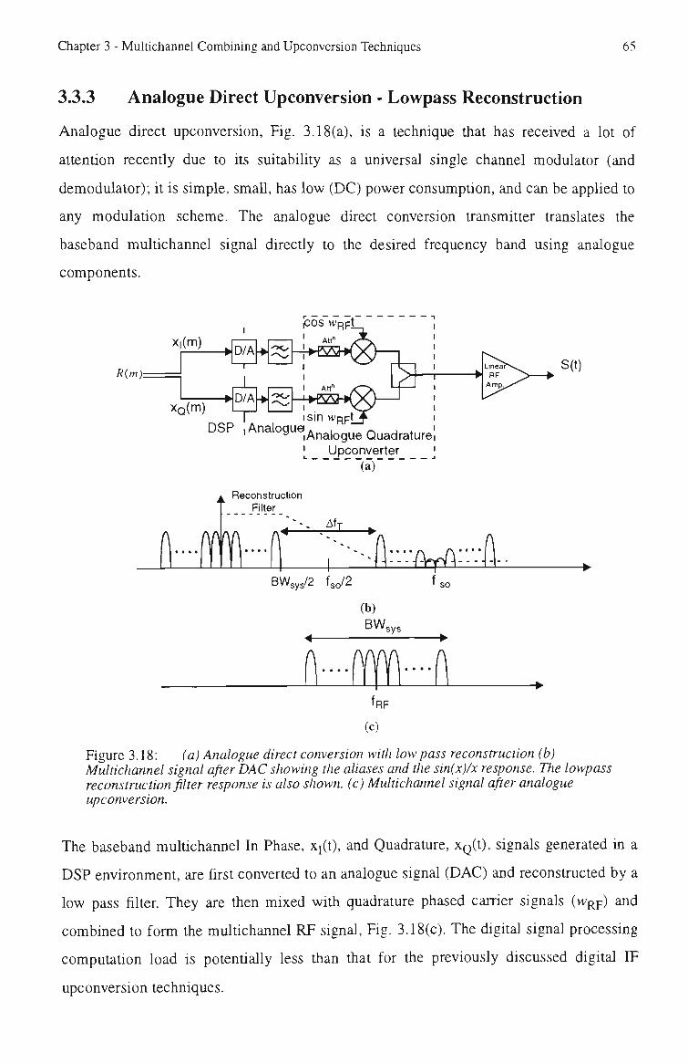
Chapter 3 - Multichannel Combining and Upconversion Techniques 65
3.3.3 Analogue Direct Upconversion - Lowpass Reconstruction
Analogue direct upconversion. Fig. 3.18(a), is a techitique that has received a lot of
attention recentiy due to its suitability as a ultiversal single channel modulator (and
demodulator); it is simple, small, has low (DC) power consumption, and can be applied to
any modulation scheme. The analogue direct conversion transmitter translates the
baseband multichannel signal directly to the desired frequency band using analogue
components.
R(m):
X
—^——
xc
(m)
3(m)
D/A ' • r -
1 D/A
1 DSP (Analogue
sin w Analogue Quadrature ' _ _Upconvej;ter
" ' " ( a )
Reconstruction Filter
Af.
>2Jk BWsys/2 fso/2
•y --' f
so
(b) BWs
M — • 'sys
fRF
(c)
Figure 3.18: (a) Analogue direct conversion with low pass reconstruction (b) Multichannel signal after DAC showing the aliases and the sin(x)/x response. The lowpass reconstruction filter response is also shown, (c) Multichannel signal after analogue upconversion.
The baseband multichannel In Phase, Xj(t), and Quadranire, XQ(t), signals generated in a
DSP environment, are first converted to an analogue signal (DAC) and reconstructed by a
low pass filter. They are then mixed with quadrature phased carrier signals (vv^p) and
combined to form the multichannel RF signal. Fig. 3.18(c). The digital signal processing
computation load is potentially less tiian tiiat for the previously discussed digital IF
upconversion techniques.

Chapter 3 - Multichannel Combining and Upconversion Techniques 66
3.3.3.1 Computational Requirements
Calculation of the analog direct upconversion computational reqturements wtil assume a
multistage interpolation technique using halfband interpolators:
CADU = 2.{stage l}.fs.comb + 2.{stage 2}.2.fs.conib + • - + 2.{(stage j)}.fso (3.30)
The computational power (in MOPS) versus the output sampling frequency has then been
plotted for both the GSM and MPT1327 systems, Fig. 3.19.
20 40 60 80 Output Sampling Frequency (MHz)
100
Figure 3.19: Computation power required to interpolate and quadrature upconvert a multichannel signal for analogue direct conversion. Parameters are BW^j, = 5 MHz, fs-comb 6.5 MHz: MPT 1327 - alias attenuation = 82 dBc; GSM - alias attenuation = 61.8 dBc
The computational load for the analog direct upconversion is greater than that for the two
digital upconversion techniques, Eqn (3.20) and Fig. 3.11, for a given output samphng
frequency. However, the output sampling frequency (computation load) is potentially a lot
lower for analog direct upconversion. Digital IF upconversion requires a samphng
frequency of 104 MHz to achieve an intermediate frequency of 26 MHz, whereas to
achieve approximately the same intermediate frequency, subsampling upconversion will
require a sampling frequency of 26 MHz. The resulting 8 MHz of transition width allows
for the practical implementation of the bandpass reconstruction filter. Analogue direct
upconversion requires only a sampling frequency of only 13 MHz to achieve the same 8
MHz of transition width.

Chapter 3 - Multichannel Combining and Upconversion Techniques 67
A sampling frequency of 13 MHz translates to 208 & 286 MOPs of computation for GSM
and MPT 1327 systems respectively. The computation load for analog direct upconversion
is therefore significantly lower than digital IF upconversion and marginally lower than
subsampling upconversion. Unfortimately, analogue quadrature upconverters have a well
known source of linear error, namely the amphtude and phase imbalance (mismatch)
between the I and Q paths [43], and this is a significant problem.
3.3.3.2 Linear Errors
Different phase and amplitude responses introduce most of the imbalance between the I
and Q paths. Additionally, some phase imbalance can be attributed to the local oscillator
signals not being in exact quadrature; due to the non-ideal characteristics of the mixers
and phase splitter.
Sideband; Carrier Rejection I Leakage
T Undesired A f Sideband [
Desired Sideband
-^ I frequency 'c
Figure 3.20: Error signals in an quadrature upconverter
The imbalances result in an undesired (image) sideband. For example, if a single sideband
(SSB) tone is output through the quadramre upconverter, then the resulting signal wiU
consist of the desired sideband, an undesired sideband and some carrier leakage, as shown
in Fig. 3.20. If the imbalances are small then it can be shown that the power ratio of the
undesired to desired sideband (referred to as the sideband rejection) is [21]:
Sideband ReJec.o„(SR) = lOloJ^-^^^^^^] - W^Ua^ .^^^^Bo (3.31) desired sideband J \4\ ^
where a and Og are the relative gain and phase mismatch between the I and Q paths
respectively. It is reasonable to talk of component imbalances (neglecting the
reconstruction filters) of 0.3 dB and 3° in a weU designed analogue quadrature
upconverter. Imbalances of this magnitude would resuh in -30 dBc of sideband rejection,
sufficient for some single channel applications.
The multichannel apphcation highlights a unique problem due to the need for tighter

Chapter 3 - Multichannel Combining and Upconversion Techniques 68
control of the amplitude and phase imbalance compared to the single channel case. When
a multichannel signal, Fig. 3.21(a), is passed through an unbalanced quadrature
upconverter, the resulting sideband signals. Fig. 3.21(b), wiU either fall into an occupied
channel or an unoccupied channel. Analysis of these two cases gives insight into tiie
amount sideband rejection, or imbalance, that can be tolerated.
-BWsys/2
Power Control
(a) Bwsys/2 frequency
T Sideband Rejection
frequency (b)
Figure 3.21: (a) Ideal multichannel signal before upconversion displayed in complex baseband format, (b) Desired and undesired (image) signals after imbalanced quadrature upconversion. Note that channel 2 is not activated and channel 3 is subject to power control. In both these situations, the image signal of channel 7 and 6 are more of a problem.
If the sideband signal falls into a channel that is currentiy being transmitted, it will cause
distortion (shown shaded in Fig. 3.21(b)). This is similar to the self distortion that occurs
for a single channel quadrature modulator. The required sideband rejection is related to the
carrier to noise performance of the modulation (for a given bit error rate). The GSM
system will operate at a 9dB carrier to noise ratio at the receiver. The distortion introduced
by the imbalances of the transmitter would need a margin of around 6 dB below this level
so that there is no noticable effect. Additionally if power control is employed (30 dB from
GSM specifications, channel 3 in Fig. 3.21(b)) then sideband rejection at the transmitter
should be greater than -45 dBc so not to affect the error rate performance of the system.
The sideband signal could equally fall into a vacant channel position (the image of channel
7 falling into the vacant channel 2, Fig. 3.21(b)). In tiiis situation the system must meet the
spurious emission level specification. For the GSM system with an 8th power class
transmitter. Fig. 2.5(a), the SR specification would be -61.8 dBc, whereas for the
MPT1327 system. Fig. 2.5(b), the SR specification is more stringent at -82 dBc. The

Chapter 3 - Multichannel Combining and Upconversion Techniques 69
tolerance of phase and amplitude unbalance is illustrated in Fig. 3.22. Obviously the
analogue quadrature upconverter is not practically usable in a multichannel environment
without some form of refinement that corrects tiie amplitude and phase imbalance. A
novel technique for correcting these imbalances wiU be introduced in Chapter 4.
-61.8 dBc
-0.2 -0.1 -0,05 0 0.05
Pnase ImbaancB (degrees)
Figure 3.22: To meet a given amount of sideband rejection, the corresponding phase and amplitude imbalance must fall within the boundary indicated.
Carrier leakage. Fig 3.20, is another source of error. It is caused by the lack of local
oscillator isolation in the mixer, and by any DC offsets in the I and Q paths. DC
compensation techniques used in single channel applications [25-26] can be utilised to
suppress the carrier leakage component.
3.3.3.3 DAC Interface
The lower output sampling frequency of analogue quadrature upconversion will lessen the
speed requirements of the DAC interface. The minimum output sampling rate of the DAC
is 6.5 MHz for a system bandwidth of 5 MHz. This is lower than that of the previous two
upconversion techniques. The value of sampling frequency would be higher if
oversampling is incorporated to reduce the reconstruction filter complexity. For a
combining sampling frequency of 6.5 MHz, the filters transition bandwidth (Afj) is 1.4
MHz. Interpolating the complex baseband multichannel signal by a factor of 2 (f ^ = 13
MHz) will increase the transition bandwidth to 8 MHz, a factor of 6 times larger than the
previous value. Therefore the reconstruction filter wiU be much simpler.
Two consequences of increasing the oversampling ratio are the additional computation
and the increased speed of the DAC. The latter is less of a problem compared to the
previous digital IF techniques because the multichannel signal is contained at baseband,
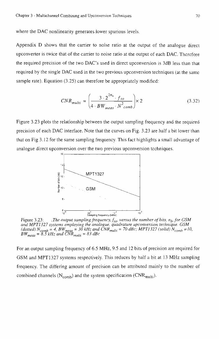
Chapter 3 - Multichannel Combining and Upconversion Techniques 70
where the DAC nonlinearity generates lower spurious levels.
Appendix D shows that the carrier to noise ratio at the output of the analogue direct
upconverter is twice that of the carrier to noise ratio at the output of each DAC. Therefore
the required precision of the two DAC's used in direct upconversion is 3dB less than that
required by the single DAC used in the two previous upconversion techniques (at the same
sample rate). Equation (3.25) can therefore be appropriately modified:
CNR multi 3 - 2 ^ " ^ / .
V4 • BW^^^_^ • N comb) x 2 (3.32)
Figure 3.23 plots the relationship between the output sampling frequency and the required
precision of each DAC interface. Note that the curves on Fig. 3.23 are half a bit lower than
that on Fig 3.12 for the same sampling frequency. This fact highlights a small advantage of
analogue direct upconversion over the two previous upconversion techniques. l E r
10' 10 Sampling frequency (MHz)
Figure 3.23: .The output sampling frequency, f^g, versus the number of bits, ny, for GSM and MPT 1327 systems employing the analogue, quadrature upconversion technique. GSM (dotted) N^g^h = 4, BW^^„, = 30 kHz and CNR^^ij^ = 70 dBc; MPT1327 (solid) N^^^f, =10, B^meas = ^-^ ^^^^ ««^ CNR^^in = 83 dBc
For an output sampling frequency of 6.5 MHz, 9.5 and 12 bits of precision are required for
GSM and MPT 1327 systems respectively. This reduces by half a bit at 13 MHz sampling
frequency. The differing amount of precision can be attributed mainly to the number of
combined channels (N^omb) ^^^ ^^^ system specification (CNR^miti)-

Chapter 3 - Multichannel Combining and Upconversion Techniques 71
3.3.4 Analogue Direct Upconversion - Bandpass Reconstruction
This technique of upconversion utilises the quadramre upconverter structure but rather
than reconstructing the signal using lowpass filters immediately after the DAC's, the
signal reconstruction occurs in a bandpass filter after the quadrature upconverter. Fig
3.24(a). This removes one source of amplitude and phase imbalance, which is significant
in a multichannel situation as will be seen in the chapter 4.
cos WRpt
R{m}.
X
X(
(m)
2(m)
D/A 1
1 D/A
r r^sin vvRpt
DSP ' analogue
(a)
BWsys/2 fs/2
Afj < M -
'L=f{\:
(b)
BW sys Bandpass Reconstruction Filter
JTl ^
fpt u— (c)
Figure 3.24: (a) Analogue direct upconversion- bandpass reconstruction architecture (b) Ideal multichannel signal after DAC showing the alaising components ajid the sinx/x response (c) Multichannel signal after RF upconversion showing the bandpass reconstruction filter characteristic.
The bandpass reconstruction filter must attenuate the digital aliasing signals that are stiU
present from the sampling process. Fig. 3.24(c), and it will have a similar performance
requirement to the previously described sub-samphng upconverter, although the centre
frequency is now the final RF transmitting frequency.
3.3.4.1 The Bandpass Reconstruction Filter
The RF transmitting frequency will depend on the radio system. Currentiy cellular and
trunking radio systems are operated at around 900MHz, whtist future PCS systems wtil
operate in tiie 1.8 GHz frequency band. These two frequencies will now be used to

Chapter 3 - Multichannel Combining and Upconversion Techniques 72
tilustrate the bandpass filter design requirements.
This example will again assume that tiie baseband multichannel signal has been
mterpolated by 2 (f o =13 MHz) to widen the filter transition bandwidth. The amount of
computation power is the same at 208 MOPS for GSM and 286 MOPS for MPT1327.
The filter %BW is quite small because of the high final centre frequency. Table 3.6. The
best choice of technology for both the 900 MHz and the 1.8 GHz band is therefore the
cavity (coaxial) or dielectric resonators, although SAW (transversal or coupled-resonator)
filters could be apphed at the 900MHz band. SAW filters are not practical at 1.8GHz [41].
Table 3.6: Example to achieve a final RF transmission frequency of900MHz and 1.8GHz.
L
2
Centre frequency
900 MHz
1.8 GHz
BW3dB (MHz)
5.5
%BW
0.6%
0.3%
Tech^
SAW Cavity
DR
Cavity DR
Afj (MHz)
7.5
SF
3.7
5s (dB)
61.8
82
Order^
5
6
a. Tech - Technology chosen using Reference [41] b. Order - From Fig. 3.15.
The bandpass filter requires a filter order of 5 or 6 which is practical in at least two
technologies. Table 3.6.

Chapter 3 - Multichannel Combining and Upconversion Techniques 73
3.4 Conclusion
This chapter focused on the use of DSP combining for multiple channels in a frequency
division multiplex format and the frequency translation of the multichannel signal to RF.
The combining of multiple channels consists of a sample rate interpolator, a multiplier and
a summer. To minimise the computational load three interpolator techniques were
investigated. Cascaded halfband interpolator stages were shown to be more efficient than
the polyphase FFT technique for less than 8 channels. The polyphase FFT technique
mcorporates the interpolator, multiplier and summer mto one efficient algorithm and the
computation load is constant regardless of the niunber channels combined. The memory
LUT approach is usable for digital modulation schemes, where the number of output
states (trajectories) is small enough not to require an excessive amount of memory. The
modulated signal is generated at the higher sampling frequency directiy from the LUT,
eliminating the need for an interpolation (filtering) stage. This technique has the lowest
computation load with only modest memory size and access speed requirements.
The computation load of multichannel combining is dependent on the radio system and
the number of channels to be combined, N^Q^H,. The GSM cellular radio system needs 124
MOPS (the equivalent of 5 general purpose C40s) to combine 4 channels using the
memory LUT approach, whereas the trunking radio system, MPT1327, requires 780
MOPS (the equivalent of 32 general purpose C40s) to combine more than 8 channels.
The final sections of the chapter discuss the upconversion of the multichannel signal to RF.
Four dtiferent techniques are summarised in the first column of Table 3.7. All techniques
required further sample rate interpolation before upconversion to RF.
Digital IF upconversion translates the baseband mititichannel signal to an intermediate
frequency at a quarter of the output sampling frequency. There is a need for a very high
performance DAC, which presentiy limits the intermediate frequency to approximately 25
MHz (a samplmg frequency of 100 MHz). However, pubhshed results (Appendix C)
suggest that DAC's capable of 1 GHz sample rates and of sufficient performance witi soon
be available.

Chapter 3 - Multichannel Combining and Upconversion Techniques 74
Table 3.7: Summary of the four different upconversion techniques.
Upconversion Technique
Digital IF
Subsampling
Analogue Direct -LPF
Analogue Direct -BPF
Computation Power (MOPS)
GSM
1100
312
208
208
MPT1327
1400
442
286
286
DAC Precision (nj,)
GSM
8
9
9
9
MPT1327
10.5
11.5
11.5
11.5
Upconverter Stages
Quadrature
1-digital
1 -digital
1-analogue
1-analogue
Heterodyne
2
l->2
0
0
Main design issues (in order of importance)
(i) Computation Power. (ii) DAC Performance
(i) Analogue IF limited by DAC (ii) Sin(x)/x compensation, (iii) Bandpass Filter
(i) Linear Errors - esp. LPF (ii) DAC Performance
(i) Linear errors (ii) DAC performance (iii) Bandpass Filter
The main disadvantage of the digital IF upconversion technique is the computational
requirements of the interpolation process. Between 1100 and 1400 MOPS are required to
achieve an IF of 26 MHz using halfband filters. The implementation of more efficient
interpolation architectures [38-40] could lower the amount of computation required. In
addition improvements in technology witi make this technique more viable in the future.
Subsampling upconversion, substantially lowers the computational requirements of the
previous technique. This technique uses a bandpass filter to select an alias of the DAC
output signal rather than the fundamental. A higher analogue intermediate frequency can
be obtained and thus the potential exists for eliminating one of the following heterodyne
stages.
A disadvantage of subsampling with wide channel bandwidths is the amphtude variation
(up to 20 dB) caused by the sin(x)/x roll-off Correction for amphtude variation is
necessary and will require additional computation. The ultimate analogue IF is also
hmited by the performance of the DAC, which degrades as the frequency increases.
Therefore at the frequency of the selected alias, the DAC must exhibit performance
consistent with the precision stated in Table 3.6. The bandpass filter is not seen as a
hmiting factor here.
The last two techniques consist of translating the baseband multichannel signal directiy to
RF using an analogue quadrature upconverter. Both schemes are very similar in design.

Chapter 3 - Multichannel Combining and Upconversion Techniques 75
one reconstructs the signal with a LPF whilst the other uses a BPF. Compared to the digital
IF techniques, analogue direct upconversion has the advantages of low computation power
and a lower performance DAC. Therefore, analogue direct upconversion justifies further
study.
Unfortunately, amplitude and phase imbalances, inherent in the analogue quadrature
upconverter, require compensation. A new technique of compensation to overcome the
phase and amphtude imbalances will be investigated in the next Chapter.
The performance, in terms of SFDR, of the DAC is degraded by the step nonlinearity. A
pre-processing algorithm used to overcome the step nonlinearity and improve the SFDR
wtil be investigated in Chapter 5 and the implementation discussed in Chapter 6.

Chapter 4
The Effect of Reconstruction Filters on Analogue Direct Upconversion
4.1 Introduction
The previous chapter highlighted the issue of phase and amplitude imbalance in an
analogue quadrature upconverter and the need for circuitry to correct the frequency
dependent phase and amplitude imbalances.
In Section 4.2, an adaptive compensation technique is introduced as a means of
overcoming frequency dependent imbalances. Whereas previous compensation techniques
have only compensated for a single gain and phase imbalance, this novel compensation
method cancels the undesired sideband at a number of frequencies across the system
bandwidth.
Section 4.3 shows that the reconstruction filters are a major contributor to frequency
dependent imbalances across a wide band. Previous analysis [3,44,45,25,26] has generally
neglected the significance of the effect of a mismatch in the reconstruction filters.
Although it has been reported [47] that "in a predistortion linearising system the
reconstruction filters are a major source of ertor", the analysis was restricted to a single
channel (narrowband) system with predistortion.
Section 4.3 also models the effect of frequency dependent imbalances on the sideband
signal. This model is then used to show that the error vector between the reconstruction
filters in the In Phase and Quadrature paths is related directiy to the amount of sideband
rejection.
76

Chapter 4 - The Effect of Reconstruction Filters on Analog Direct Upconversion 77
Section 4.4 uses the relationship found in Section 4.3 to develop a methodology for
analysing the effect of mismatched filters driving an analogue quadrature upconverter.
Two parameters, oversampling ratio and the 'channel to system bandwidth' ratio, are
introduced to objectively judge the performance of the multichannel adaptive
compensation technique.
The analysis of the classical ati-pole filter equations reveals the sensitivity of filter order,
filter type, percentage mismatch and a differing sideband rejection specification in the
novel compensation technique. The results of this analysis for different radio systems
relate the amount of oversampling required for the compensation technique to achieve the
required sideband rejection.
Finally, Section 4.5 proposes the use of bandpass reconstruction to avoid the frequency
dependent mismatch problems of the lowpass reconstruction filters.
4.2 A Novel Method for the Compensation of Gain and Phase
Imbalances
A number single channel correction techniques for amplitude and phase imbalances of
quadrature upconverters currentiy exist [44,45,25,26]. Implementation of one correction
technique which utilised the CRISIS network [26], adjusted the gain and phase imbalances
to 0.02 dB and 0.4° respectively. This is equivalent to -49 dBc of sideband rejection, Eqn.
(3.31), which constitutes a definite improvement, but is unacceptable in multichannel
applications. Additionally, the effectiveness of current compensation techniques decreases
dramatically in the presence of frequency dependent imbalances.
The novelty of the compensation technique presented revolves around the multichannel
combining algorithm, which could take any of the forms discussed in Section 3.2. Figure
4.1 illustrates the proposed technique. Channels 1, 5, 8 and N -h are combined, N -o b = 4,
through a multichannel combining algorithm to form the complex baseband signal. The
resultant signal is then interpolated by a nominal factor of L, before being output through
the digital to analogue converter. The oversampled multichannel signal lessens the
complexity of the reconstruction filters as will be shown later in the chapter. The
oversampled complex baseband signal is finally upconverted to RF via an analogue
quadrature upconverter.

Chapter 4 - The Effect of Reconstruction Filters on Analog Direct Upconversion 78
The inherent gain and phase imbalances of the upconversion scheme will cause undesired
sideband signals. The compensation method deliberately introduces a signal component
into the image (where the undesired sideband exists) channel. From Fig. 4.1. channel 5 is
transmitted and requires correction. The conjugated signal component is then introduced
into the image channel, N(.ij-4, and the complex coefficient (Cj^) is adaptively adjusted
until the undesired sideband is cancelled.
The adaption technique measures the sideband power in a vacant channel using a tuned
receiver (error sensing circuitry in Fig. 4.1) and adjusts the complex coefficient (C^,) to
minimise the power of the undesired signal.
C h 1
Oh 5
C h 8
C h (Neh-4)
ChN,h
s-mod
MTw
v>.t:
>•< O D.
S-comb fso=L . i
Interpolate - I Algorithm
s-comb ( i_ D/A
• D/A
"n n
cos Wopt
i.
DSP f
Sin Wqpt
Adaption Algorithm
Error Sensing Circuitry
(a)
C h 1 .
C h S -
C h 8 .
Ch (Nch-4>
ChNch
s-mod 's-comi:
LUT
LUT
-«LUT
^;LUTi
- • LUT
fso=L . f, S-comb
Interpolate Algorithm
0' i ; ^
DSP
Adaption Algorithm A/D
Error Sensing Circuitry
(b) Figure 4.1: Multichannel adaptive compensation technique for correcting gain and phase imbalances using the (a) polyphase FFT combining algorithm or the (b) LUT algorithm. Channel N^^.4 is the image of Channel 5.
The process described above is repeated for every channel in the system but only whilst
the channel is vacant. The update rate is slow, but this is not considered a problem as the

Chapter 4 - The Effect of Reconstruction Filters on Analog Direct Upconversion 79
gain and phase imbalances drift slowly with time. The polyphase FFT combining
technique. Fig. 4.1(a), gives access to all channels and the correction algorithm will only
require one additional complex multiply operation per active channel at the low fj.mod
sample rate. Other schemes. Fig. 4.1(b), will need the correction algorithm to operate at
the higher fg-comb sample rate.
The compensation technique described has a number of advantages over previous adaptive
correction techniques:
• Reduced Computational Load - The adaption algorithm and the scaling coefficient operate at the channel or combining sampling rate, as opposed to the output sampling rate [25,26,44-46].
• Ability to Correct for Frequency Dependent Imbalances across the System Bandwidth - Previous techniques only compensate for a single bulk gain and phase imbalance across the system band.
• Increased Sensitivity of Feedback Signal - This technique detects only the undesired signal, as opposed to both the desired and undesired signal [26], thus increasing the dynamic range of the correction network.
For an uncorrected analogue quadrature upconverter the power of the sideband will
invariably exceed the spurious emission specification (Fig. 2.5), and it is therefore
necessary to reduce the power in the sideband to comply with this spurious specification.
The amount of sideband rejection required to meet the spurious specification was
calculated in Section 3.3.3.2, for GSM and MPT1327 radio systems; it is -61.8 dBc and
-82 dBc respectively.
The multichannel compensation technique also exploits the fact that there is room for non-
ideal cancellation by cancelling the phase and gain imbalance at a single frequency (bulk
imbalance). The sideband will be completely removed at this frequency. However, the
frequency dependent imbalances mean that a differential phase and gain imbalance will
remain across the remainder of the channel (differential imbalance), causing a residual
sideband response. Fig. 4.2(b). The residual sideband response must be kept below the
sideband rejection specified for the radio system.

Chapter 4 - The Effect of Reconstruction Filters on Analog Direct Upconversion 80
Uncompensated Sideband
BW
BW
Phase Imbalance
sys (a)
GainTmbalance
. frequency
Residual Sideband
Phase Imbalance
hA Cancellation frequency/
(b)
alance frequency
Figure 4.2: (a) Sideband response due to frequency dependent imbalances (b) Sideband response after cancellation of the channels bulk imbalance.
To comply with the amount of the sideband rejection required, the following condition
must hold:
5^^j PowerinSideband ^g^ Power in Signal (4.1)
The ability to quantify the frequency dependent imbalances is the next step in analysing
the performance of the multichannel adaptive compensation technique.
4.3 Analysis of Frequency Dependent Imbalances
4.3.1 Causes of Frequency Dependent Imbalance in an Analogue
Direct Upconverter
Frequency dependent gain and phase imbalances arise from both the quadrature
upconverter and the mismatch in the reconstruction filters.
The quadrature upconverter consists of the mixer, phase splitter and summer components.
The gain and phase through each of these components is to some extent dependent on
frequency, although the amount of dependence will depend on the complex design
strategies employed. However, these issues lie beyond the scope of the thesis.
A typical Mini Circuits IQ modulator was chosen as an example (Table 4.1 generated from

Chapter 4 - The Effect of Reconstruction Filters on Analog Direct Upconversion 81
the Mini Circuits data sheet). It can be seen that over a channel bandwidth of 5 MHz.
around -54 dBc of sideband rejection exists if the bulk imbalance is removed (leaving the
differential imbalance). Over -70 dBc could be achieved if the bandwidth was reduced
below 100 kHz.
Table 4.1: Absolute variation of gain and phase imbalance across a specified bandwidth for a Mini Circuits IQ Modulator (MIQD 895).
_ J . . , Differential gain Variation Differential Phase „. . . ,_ . Bandwidth ,!L, , , , . ^ Sideband Rejection
(dB) Variation (degree)
100 kHz
.500 kHz
5 MHz
0.01
0.02
0.05
0.05
0.10
0.30
70 dBc
64 dBc
54 dBc
In most communication systems utilizing the FDM format the channel bandwidth is less
than 200 kHz. Therefore, the quadrature upconverter, with a single point of cancellation,
will achieve significant suppression of the undesired sideband to around 70 dBc. A larger
amount of sideband rejection will occur when more compensation points are used. Thus,
frequency dependence will be apportioned entirely to the reconstruction filters, which will
now be analysed with respect to the compensation technique.
4.3.2 IMathematical Analysis - The Effect of Filter Mismatch on the
Sideband Signal
To analyse the effects of filter mismatch, the reconstruction filters are modelled with
relative gain mismatch, a(/), and phase error from quadrature, <i> ,(/) (radians). The
variable P(/) is used to account for the absolute attenuation characteristic (or gain transfer
function) of the filter and serves to normalise the magnitude at any frequency.
The gain of the I path will be given by the transfer function, |3(/), of the ideal filter in
question:
P(/) = |i(/)(l+(«(/)/2)) - M/) • a(/)/2 (4.2)
and the gain of the Q path will be given by a percentage change, p(/) «(/) , in the transfer
function of the ideal filter:
P(/)(l+a(/))= |3(/)(l+(a(/)/2)) -|- p(/) • a(/)/2 (4.3)

Chapter 4 - The Effect of Reconstruction Filters on Analog Direct Upconversion 82
Similariy, the phase mismatch between the filters is split equally between the two paths.
o^(/)/2. The quadrature upconverter and DAC's are assumed to be ideal. These
assumptions isolate the reconstruction filters as the source of error. Fig. 4.3 presents the
summary of the model:
Figure 4.3: Modelling the mismatch between reconstruction filters
The quadrature signal that is driven from the DSP, can be represented as a complex signal
with a real (I channel) and an imaginary (Q channel) component. The same signal can be
represented as a vector with an instantaneous magnitude and phase:
r ( r ) = Xf{t)+jx^{!)
(4.4)
If there is no mismatch between the filters then the upconyerted signal is given by:
s(t) = Re\r(t)- e ' (4.5)
The mismatch in the reconstruction filter design causes the original signal to be distorted
(undesired sideband) when it is translated to the carrier frequency. The output, s(t), from
the quadrature upconverter shown in Fig. 4.3 is given by the following equation:
.v(r) = Re
; e ( / ) (^.•sll
P ( / ) h + ^
+ P(/)f^)-
|,(,)|,V-'^C0S^^^J +
.lKOk-'«"'s>n(!£^^) J
; » • '
V 2
^jkOir^^^^sin^-^JJ -ye(o.;_f^c-(/)^
- / v v /
(4.6)

Chapter 4 - The Effect of Reconstruction Filters on Analog Direct Upconversion 83
After mathematical analysis Eqn. (4.6) can be shown to be equivalent to:
|3(/)(l+^]cos(^^j|r(0|cos((o^f + e(/))-
P(/)( l+^)sin(-^)r(f) |s in((o^t-e(r)) + s(t) =
P(/)(^)cos |^^] | r(0 |cos(co,r-e(0) +
P(/)(^)in( '^)k(r) |sm(co^,r + e(r))
(4.7)
Equation (4.7) mathematically describes four signals generated by the mismatch between
the reconstruction filters. By selecting a complex plane referenced to the carrier frequency
of the quadrature upconverter, the four signals can be represented as baseband complex
vectors:
uAt) = P(/) 1 + a(/) eif)\ ;cos f - ^ J •r(t) (4.8)
„ (0 = P(/)(^>.n(^y^-r(r) (4.9)
.,(0 = P ( / ) ( ^ > o s ( ^ l . , - * ( 0 (4.10)
v.CO = P(/) 1 + ) s , n ( ^ (4.11)
The vectors have been classified as a desired (u(t)) signal or a sideband (v(t)) signal. The
desired signals are determined from the fact that they rotate in the same direction as the
original signal, r(t), whereas the sideband signals rotate in the reverse direction, thus
appearing in the image channel position illustrated in Fig. 4.2(b).
v(t).
^s^^y. /V2(t)
, v Vi(t)
(a)
ui(t)
(b)
Figure 4.4: Vector representation of (a) Undistorted signal - r(t) (b) Distorted signals due to direct conversion imbalances.

Chapter 4 - The Effect of Reconstruction Filters on Analog Direct Upconversion 84
Fig. 4.4(a) represents the original signal upconverted to the carrier frequency by an ideal
quadrature upconverter. If the quadrature upconverter is non-ideal, as modelled in Fig. 4.3.
the original signal will be distorted to form four vectors as shown in Fig. 4.4(b). and
described by Eqn. (4.8) to (4.11). The sideband signal is therefore the vector sum of Eqn.
(4.10) and (4.11):
.(,) = .(,).p(,)rr^)]cosr^]./,.«4^),nf^')] (4.12a)
.(0 = .H.)-P(/)("4^./>-.^]^] (4.12b)
Eqn. (4.12a) shows that the sideband signal can be represented as the complex conjugate
of the original signal multiplied by a complex coefficient, which is a function of both gain
and phase imbalance. For small phase error the sideband signal can be approximated by
Eqn. (4.12b) and therefore expressed as an absolute magnitude:
, ,„J.(-)l P ( / ) > ( / ) ^ ^ (4.13)
From the vector addition of Eqn. (4.8) and (4.9), the approximate magnitude of the wanted
signal can be shown to be approximately |r(/)| p(/). Therefore, the amount of Sideband
Amplitude Rejection ratio (SAR) is given as the absolute magnitude of the image vector,
divided by the absolute magnitude of the wanted signal, the form of which is the same as
in the static case analysed in [3]:
SAR= 1^^ (4.14)
2
Note that the sideband rejection (SR) ratio is equal to the SAR ratio squared.
An alternative way of visualising the previous analysis is to consider the I and Q path
filters as vectors. When they are matched, they are both equal in magnitude and phase
(Fig. 4.5(a)), subsequentiy causing no distortion or sideband response. When the filters are
mismatched, there exists a phase and gain difference (frequency dependence). This is
illustrated in Fig. 4.5(b).

Chapter 4 - The Effect of Reconstruction Filters on Analog Direct Upconversion 85
P(/)' P(/) ^(f)-"" ' p(/)a(/)
(a) (b)
Figure 4.5: (a) I and Q path filters matched (b) I and Q path filters mismatched
It can be shown that the error vector is related to the SAR ratio by:
SAR = le(/}l/2xp(/) (4.15)
This can be verified by calculating the magnitude of the error vector in Fig. 4.5(b) for
small gain and phase imbalances and comparing it to the approximate SAR calculated in
Eqn. (4.14). For typical values of sideband rejection in multichannel radio systems, the
sideband has to be of a magnitude that implies very small gain and phase mismatch. The
magnitude of sideband rejection can now be accurately predicted from Eqn. (4.15) and
used as a means of objectively judging the performance of the multichannel compensation
technique.
4.4 Analysing the Effect of Mismatched Reconstruction Filters.
4.4.1 The Methodology
The methodology calls for a relative comparison of performance when adjusting
parameters relevant to filters. It is based on modelling the mismatch between the filters as
a percentage increase in the cut-off frequency of one filter. This has limitations, especially
when considering the real implementation issues of filters, but for practical analysis
purposes it is seen as a realistic yardstick. The relative performance of a particular filter
will then be judged by two parameters, the oversampling ratio and 'channel to system
bandwidth' ratio.

Chapter 4 - The Effect of Reconstruction Filters on Analog Direct Upconversion 86
IN BAND OUT OF BAND
Digital Alias
Sin(x)/x Function
BWsy3/2
Figure 4.6: Overview of Communication System Parameters relevant to Direct Upconversion and a Multichannel Environment.
For the purpose of analysis, the communication system will be described by:
• channel bandwidth - BW^h
• system bandwidth - BW^yj
• and the amount of sideband rejection - SR.
The channel and system bandwidth parameters can be combined to give the total number
of channels across the system bandwidth (not the same as the number of combined
channels [Ncomb])-
BW ch BW
(4.16) ch
The number of channels indicate the total number of cancellation frequencies available
across the system bandwidth, using the novel cancellation technique.
Adherence of the sideband rejection specification implies the following two objectives:
• In System Band: Given a percentage mismatch between the two quadrature filters, the amount of sideband rejection in the image channel must comply with Eqn. (4.1).
• Out of System Band: The digital alias must be attenuated below that indicated by the same sideband rejection specification. This is achieved by the reconstruction filter (A2) and the sin(x)/x response of the digital to analogue converters (Al).
The number of cancellation frequencies, i.e. the number of channels across the system
bandwidth, is derived solely from the Tn System Band' objective. The mismatch between
the filters creates frequency dependent imbalances that require periodic cancellation

Chapter 4 - The Effect of Reconstruction Filters on Analog Direct Upconversion 87
across the system band to meet a given sideband rejection. The worse the mismatch
between the filters, the smaller the channel bandwidth must be so that after cancellation,
the power of the residual sideband complies with the spurious specification. For a fixed
system bandwidth, this can be equally expressed as more channels. The number of
channels, or compensation frequencies, is essentially a measure of the frequency
dependent mismatch in the system.
To illustrate how the number of channels is calculated, a fifth order Butterworth filter is
used as a case study. The error vector between the two filters is used to calculate the
sideband rejection Eqn. (4.15). Fig. 4.7(a) illustrates the amount of sideband amplitude
rejection ratio for a 5% mismatch in the reconstruction filters cut-off frequency. Note that
the filters cut-off frequency has been normalised to 1 radians/second. Here the filters are
perfectly matched at DC (no sideband), whilst a sideband magnitude exists throughout the
passband, due to the frequency dependent imbalance.
To calculate the number of channels needed for effective cancellation of the sidebands, it
is more instructive to view the gradient of the SAR across the passband of the filter, as
illustrated in Fig. 4.7(b), i.e. the larger the gradient, the more frequent cancellation should
occur.
The multichannel adaptive compensation technique will cancel a single frequency in every
channel. Total cancellation across the entire channel band, however, does not occur.
Imperfect cancellation will result in a residual sideband, as shown in Fig. 4.2(b).
T3 c0,04 CO
XI 01 S 0.02
03
Frequency (radians/sec)
(a)
Frequency (radians/sec)
(b) Figure 4.7: Fifth order Butterworth filter with 5% mismatch in the cut-off frequency (a) Sideband a?nplitude rejection ratio (b) Gradient of sideband amplitude rejection ratio.

Chapter 4 - The Effect of Reconstruction Filters on Analog Direct Upconversion 88
If the gradient is assumed constant across the channel band, a first order approximation
can be assumed for calculating the power in the sideband. That means that the sideband
amplitude resembles a triangular function and therefore the sideband power approximates
a square law function. This assumes a uniform distribution of signal power across the
channel bandwidth, Fig. 4.2(b).
It is assumed that in a worst case scenario, the largest gradient to occur across the system
bandwidth (which is a fraction of the cut-off frequency) is taken as the absolute constant
gradient across any channel.
Given the above and using Eqns. (4.1) & (4.16), the minimum number of channels is
related to the systems sideband rejection specification (SR):
Nch =
BW,„><^JHS
10SR/20xVT2 (4.17)
By varying the system bandwidth, the minimum number of channels needed to comply
with the systems SR specification can be plotted as shown in Fig. 4.8(a). As expected,
more channels are needed as the system bandwidth approaches the cut-off frequency of
the filter.
0.2 0.4 0.6 0.8 1 1 2 3 4 5 6 7 8 BWsys normalised to fcgt-off Oversampling ratio - fgo / BWsys
(a) (b) Figure 4.8: Fifth order Butterworth filter with 5% mismatch in the cut-off frequency complying with a -60 dBc SR specification (a) In System Band objective (b) Combination of In and Out Of System Band Objectives.
The second objective. Out of System Band, is achieved by attenuating the sampling aliases
by an amount equal to the sideband rejection. The filter attenuation characteristic will

Chapter 4 - The Effect of Reconstruction Filters on Analog Direct Upconversion 89
determine the output sampling rate, f p, required to achieve this condition. The sampling
frequency has been normalised to the Nyquist sampling rate of the system, BW This is
expressed as the oversampling ratio:
sys
By combining the In and Out of System Band objectives, the minimum number of
channels (or cancellation frequencies) can be related to the oversampling ratio for a given
mismatch and system sideband rejection specification. Fig. 4.8(b). This methodology is
now used to comparatively analyse the performance of the filters by modifying different
parameters.
4.4.2 Numerical Computation and Analysis
The effect of mismatched reconstruction filters driving an analogue quadrature
upconverter has been shown to introduce frequency dependent imbalances. These
imbalances can be corrected by the adaptive compensation technique introduced in
Section 4.2. However, the amount of mismatch in the reconstruction filters will put certain
restrictions on the design, that is, the number of channels and the oversampling ratio
needed to comply with the systems sideband rejection specification.
By varying different filter parameters, the methodology relating the number of channels in
a communication system to the oversampling ratio can be used to analyse the effect of the
reconstruction filters on the analogue direct upconverter.
Four parameters have been considered:
4.4.2.1 Filter Mismatch
Increasing the mismatch between the filters is the same as increasing the tolerance of the
components used in implementing the filter. This effect has been modelled as a percentage
shift in the cut-off frequency.
For a small number of channels, the oversampling ratio increases with an increase in
percentage mismatch. Fig. 4.9(a). However, in a system with a large number of channels,
100 and upwards, the amount of mismatch, as long as it is less than 5%, becomes

Chapter 4 - The Effect of Reconstruction Filters on Analog Direct Upconversion 90
irrelevant as the oversampling lintit (vertical asymptote in Fig. 4.9(a)) for the 5th order
Butterworth filter is reached.
The oversampling limit occurs when the system bandwidth equals the cut-off frequency. It
is possible to go beyond this point by pre-emphasising the outer channels but this
alternative will not be considered here. The In System Band condition therefore
determines the minimum number of channels. Any further increase in the number of
channels will improve the undesired sideband to further below the sideband rejection
specification (In System Band condition) but will have no effect on the oversampling ratio.
This phenomenon occurs because the system bandwidth cannot be extended further and
therefore the Out of System Band objective, or the roll-off of the filter which is not
dependent on percentage mismatch, will govern the lowest oversampling ratio.
It can be concluded that the filters must be able to be designed to meet tight specifications
and also be reliably reproduced in the manufacturing process.
fi 500
m
« 100
CQ
j n 0) c c CO s: o
10 -
0)
E
Oversampling Limit i
.,J0%
-.i "' ^ 1%
500
5 m
M 100
<u c c CO
u
0)
E
10
:.
t:;:::::::::;;::::::::::"-..^ : \ . -82dBr~-~-~-
^^^^"---..-61.8 dBc
2 3 4 5 6 7
Oversampling ratio - fso / BWgys 2 3 4 5 6 7
Oversampling ratio - fjo / BWgys
(a) (b) Figure 4.9: Fifth order Butterworth filter with a 5% mismatch in the cut-off frequency, and a sideband rejection of-61.8 dBc is assumed unless otherwise stated (a) Percentage mismatch of the filter cut-off frequency varied (b) Sideband rejection specification varied.
4.4.2.2 ACI Specification
Increasing the sideband rejection specification has a similar effect to increasing the
percentage mismatch. Fig. 4.9(b) illustrates that the larger the sideband rejection, the
higher the oversampling ratio required for a fixed number of channels. This is especially
important for a small number of channels, say around 10, which for a SR specification of -
70 dBc would require an oversampling ratio greater than 8. Depending on the bandwidth

Chapter 4 - The Effect of Reconstruction Filters on Analog Direct Upconversion 91
of the channel, such a large oversampling ratio will place severe limitations on the
bandwidth of the system, primarily due to the large output sampling frequency that would
be required for the digital processing.
The oversampling limit also decreases with a lowering of the systems sideband rejection
specification. To further lower this limit, the filter order would have to be increased.
4.4.2.3 Filter Type
The filters chosen contribute one desirable characteristic each: maximum flat amplitude
response, maximal flat group delay and the steepest roll-off obtained by the Butterworth,
Bessel and Chebychev filters respectively. The cut-off frequency is defined as the
frequency for which the filter attenuation has reached 3 dB.
The Chebychev filter is shown in Fig. 4.9(c) to have the best overall performance. The
lowest oversampling limit is achieved by a higher ripple in the Chebychev filter, this is due
to the inherently steeper roll-off. It is difficult to discern from Fig. 4.9(c) whether varying
the ripple of the Chebychev filter increases performance below the oversampling limit.
However, as the ripple approaches zero the Chebychev response will approach the
Butterworth response. The Butterworth filter is comparable to the Chebychev filter,
although it consistentiy has slightly worse performance.
The Bessel filter has difficulties achieving a low oversampling ratio which is mainly due to
its relatively slow roll-off and this could be lowered by using a higher order filter. Chcby
l).5dB Chcby O.ldB
500 " ^ ^ 500
m
>• 100
5 <n 0) c c CO
CD
E z
2 3 4 5 6 7
Oversampling ratio - fjo / BWgyg 1 2 3 4 5 5 7
Oversampling ratio - fgo / BWgys
(c) (d)
Figure 4.9: Fifth order Butterworth filter with a 5% mismatch in the cut-off frequency and a sideband rejection of-61.8 dBc is assumed unless otherwise stated (c) Fifth order Chebychev (0.1 dB &0.5 dB ripple), Bessel & Butterworth Filter types (d) Butterworth 4th, 5th & 7th order filters
Chapter 4 - The Effect of Reconstruction Filters on Analog Direct Upconversion 92
4.4.2.4 Filter Order
Increasing the filter order lowers the oversampling limit because of the steeper roll-off.
Fig. 4.9(d). However, for an increase in the order of the filter there is not an equivalent
improvement in performance, because a steeper roll-off is accompanied by a larger In
System Band gradient. For example, a system with 10 channels requires an oversampling
ratio of 5 and 4.5 for a fourth and fifth order filter respectively. Whereas increasing the
order of the filter to 7 only achieves a small gain in performance; the oversampling ratio is
sttil 4.5.
In a system that has many channels it would be better to use a higher order filter as long as
the percentage mismatch could be guaranteed. The higher the filter order, the more
sensitive it is to component tolerances and its overall percentage mismatch will rise.
However, for a system with a small number of channels a lower order filter should be
employed because of its reduced complexity and comparative performance to higher order
filters.
4.4.3 Application to GSM or MPT1327 Radio Systems
The GSM radio system (class TRX 8) has twenty five 200kHz channels within a system
bandwidth of 5 MHz. This equates to 25 cancellation frequencies, using the multichannel
compensation technique. Assuming that the two reconstruction filters can be designed to
an accuracy of 5%, an oversampling ratio of 3.2 will ensure that -61.8 dBc of sideband
rejection can be achieved. Fig. 4.9(b).
The MPT 1327 specification requires a sideband rejection of -82 dBc. However, the
channel bandwidth is only 12.5 kHz, and therefore 400 channels, or cancellation
frequencies, exist across a system bandwidth of 5 MHz. Again assuming that the two
reconstruction filters can be designed to an accuracy of 5%, an oversampling ratio of 5.4
will be sufficient to ensure -82 dBc of sideband rejection. Fig. 4.9(b).
In both systems, a lower oversampling ratio could be achieved by using a similar order
(5'* ) Chebychev filter or by increasing the order of the filter. The 5% tolerance of the filter
must be assured.

Chapter 4 - The Effect of Reconstruction Filters on Analog Direct Upconversion 93
4.5 Bandpass Reconstruction
This chapter has highlighted that most of the frequency dependent imbalance in the
analogue direct upconverter is caused by the mismatch between the I and Q lowpass
reconstruction filters. The proposed design requires a 5% tolerance between the filters so
that the compensation technique can adequately correct the undesired sideband signals.
Although resistors can achieve better than 5% tolerance, capacitors will require manual
tuning to achieve this degree of accuracy. In addition, variations due to temperature will
compromise the match between the two filters. A possible solution is to employ bandpass
reconstruction.
Bandpass reconstruction operates on the RF signal and therefore does not affect the
amplitude and phase mismatch between the In Phase and Quadrature paths. The main
source of frequency dependent mismatch is therefore removed and the oversampling ratio
is also reduced to 2 (Section 3.3.4.1). In theory a single channel correction technique (i.e.
CRISIS circuit [26]) could be used to correct for the bulk amplitude and phase mismatch.
The correction circuit would have to operate at the higher output sampling frequency,
requiring a large amount of computation. The scheme described in this chapter is still the
preferred choice since it will correct for any residual frequency dependence in the
imbalances and in most cases it will normally have a lower computational load.
4.6 Conclusion
The mismatch between the reconstruction filters produces frequency dependent
imbalances which cause undesired sideband responses in an analogue direct upconverter.
A novel adaptive compensation technique has been introduced to reduce these sideband
signals to comply with radio communication system specifications. The ability to correct
frequency dependent imbalances and the fact that the correction occurs at the lower
channel sampling frequency (polyphase FFT combining) are the two distinct advantages
this technique possesses over previous adaptive compensation techniques.
The analysis of the frequency dependent imbalances yielded a relationship between the
error vector of two mismatched filters and the amount of sideband rejection. This
relationship was used to develop a methodology that related the number of channels to the
oversampling ratio, required for the new adaptive compensation technique to achieve the

Chapter 4 - The Effect of Reconstruction Filters on Analog Direct Upconversion 94
sideband rejection specification. The methodology compared the performance of the
system when four parameters were varied. The main objective was to keep the
oversampling ratio as low as possible, both for technology and power consumption
reasons.
It was found that the Chebychev filter offered the best overall performance irrespective to
the number of channels in the system. However, the order of the filter should be chosen on
the size of the system. For small systems (less than 10 channels), a low order filter offers
lower complexity with comparable performance to higher order filters. Larger systems
benefit from higher order filter, although the implementation of a higher order filter
presents an anomaly. Due to their higher complexity, they will be more sensitive to
component tolerances, and therefore their ultimate performance will be degraded.
Ultimately, the achievable tolerance of the filter is the highest priority design issue.
Through the examination of both the GSM and MPT 1327 systems, an oversampling ratio
of approximately 3.2 and 5.4, respectively, was found to be acceptable to meet the
sideband rejection specification whilst assuming that the tolerance of the reconstruction
filters could be kept to around 5%. For a system bandwidth of 5 MHz, this translates to an
output sampling frequency of 16 MHz and 27 MHz, or interpolation by a factor of 2.5 and
4.2, assuming that the original combined baseband multichannel signal is sampled at 6.5
MHz (fs.comb - Chapter 3).
The design requirement of 5% tolerance between the two lowpass reconstruction filters is
difficult to meet in an analogue environment. A way of improving the solution is to use
analogue direct upconversion with bandpass reconstruction which has a lower
oversampling requirement. Compensation for the imbalances using the technique
introduced in this chapter is also suited to this application and often requires less
computation load than previous adaptive compensation techniques.
The next chapter introduces an algorithm that enhances the performance of a DAC when
interpolation of the output sampling frequency is necessary. The algorithm can be used for
analogue direct upconversion with either lowpass or bandpass reconstruction. It is based
on the fact that a 5% mismatch in the lowpass reconstruction filters of an analogue direct
upconverter requires the baseband multichannel signal to be interpolated by a factor of 4.
This interpolation can be achieved by using two halfband stages.

Chapter 5
Enhancing the Performance of Digital to Analogue Conversion
5.1 Introduction
The digital signal processing base station employs digital to analogue conversion to
convert the multichannel signal to an analogue waveform. Chapter 3 calculated the
required DAC precision for the analogue direct upconversion technique to be equal to 9
and 12 bits, for the GSM and MPT1327 radio systems respectively. This calculation used a
system bandwidth of 5 MHz sampled at 26 MHz.
The additive white noise model for the quantisation error of a DAC was assumed in the
above calculations. Section 5.2 reviews the model and its underlying assumptions, one of
which is that the quantisation levels must be evenly spaced. A practical DAC has non-
evenly spaced quantisation levels which will generate harmonic and intermodulation
products. Dynamic errors wiU also contribute similar spurious responses, but these will
not be considered in the thesis.
Spurious responses are very important in a multichannel system, because they will fall
into neighbouring channels, above the theoretical quantisation noise floor. The spurious
free dynamic range of a DAC is therefore a very important specification for the
multichannel application. A means of improving the SFDR performance of a DAC is
through the addition of a random signal prior to quantisation.
The technique of addmg a random signal before quantisation is known as dithering.
95

Chapter 5 - Enhancing the Performance of Digital to Analog Conversion 96
Section 5.3 reviews current dithering techniques which are described by three distinct
qualities; Probability Density Function (PDF), scale and spectrum shape.
Calculation of the average quantisation transfer function in Section 5.4 yields insight into
how dither will perform in the presence of an ideal or non-ideal quantiser. The average
transfer function is used to explore the necessary scale of the digital dither required to
overcome the non-linearity of a quantiser.
Section 5.5 draws upon the previous discussions to introduce the technique of bandlimited
dithering, which is most suitable for application to multichannel base stations.
5.2 Characteristics of an Ideal and a Practical DAC
5.2.1 An Ideal DAC
The use of floating point digital signal processors allows for the very precise generation of
digital signals. In fact, the precision of such DSP's is much greater than that of any
currently avatiable DAC. This is tilustrated in Fig. 5.1(a), where n refers to the number of
information or integer bits, and m is equal to the number of fractional bits. To interface the
DSP to the DAC, the m fractional bits are truncated.
The process of digital to analogue conversion is described by the quantisation transfer
function, g(X), where the infinite precision input signal X is truncated to a multiple of a
step size, A (Fig. 5.1(b). The m least significant bits are simply ignored, whilst the n most
significant bits produce a set of discrete analogue levels. The quantisation error transfer
function, qe(X), is defined as the error between the quantiser and linear transfer function,
shown in Fig. 5.1(c), as:
g(X)=X + qe(X) (5.1)

Chapter 5 - Enhancing the Performance of Digital to Analog Conversion 97
I 1
1 (n+m) bit Internal Precision '—•/•— I I n bits
I I I Digital Signal Processor •—•/•— I i m bits
Truncated
g(X)
Linear transfer function
-3A/2
Quantiser transfer function
whereA = V„ax/2 n-1
(b) (c)
Figure 5.1: (a) The internal precision of the DSP will invariably have higher precision than that of the DAC. Truncating the m LSB's is the simplest way of interfacing the DSP to the DAC. (b) Ideal n bit DAC transfer function, g(X), given truncation of the m LSBs as shown in (a). The Ideal linear transfer function is also shown, (c) Quantisation error, qJX), of an ideal DAC.
The quantisation error is strongly dependent on the characteristics of the input signal, X,
and is quite complex to analyse. However, Bennett [56] showed that the sequence of error
samples that make up the error waveform, qe(X), are uncorrelated with each other and the
mput signal. Further, the quantisation error can be modelled as a random variable that is
uniformly distributed over a step interval. Using this model, the quantiser can be replaced
by the simple additive white noise model. Fig. 5.2, where the average power, or variance,
of the quantisation error is given by A^/12. More importantiy, this model wiU only apply
when the following conditions hold:
the quantisation levels are evenly spaced and small,
there is a large number of quantisation levels (this implies that a large number of levels are exercised), and
the input probability density function of the signal is smooth.

Chapter 5 - Enhancing the Performance of Digital to Analog Conversion 98
AP(qe(X))
.q(X)
1/A
-A/2 A/2
(a) (b)
Figure 5.2: (a) Additive noise model of a quantiser (DAC) (b) Probability density function
of the additive noise i.e. Uniform.
These conditions limit the use of the model in certain simations. For example, in the case
of a periodic sinusoid that is a sub-harmonic of the samphng frequency, only a few
quantisation levels are used, and the quantisation noise is not evenly spread, but is
concentrated into a finite number of frequencies. The additive noise model also does not
apply to Sigma-Delta ADC's because they have relatively few levels and a relatively large
step spacing. Strictly speaking, the additive white noise model does not apply to practical
DAC's because the quantisation levels are not evenly spaced.
5.2.2 A Practical DAC
A non-uniform step size (quantisation levels that are not evenly spaced) is an intrinsic
quality of a practical DAC, Fig. 5.3. This means that the transfer function passing through
the centre of each step tread is not hnear. Abuelma'atti [33-34] examined the effect of non-
ideal quantisation and came up with expressions for the amphtudes of the output
fundamental and the harmonics when the input consists of a single sinusoid [33] or
multiple sinusoids [34]. Both papers showed that the additional non-linearity may reduce
the amplitude of some harmonics, but the total distortion power in all harmonics and IM
products will inevitably be increased.
-24
-26
-28
J - 3 0
i=-32
^ - 3 4 C
^ - 3 6 Z
< -38
-42
-1
- •
l^ 0
'1
• - ^
-a
'
^^
-6
;
-4
'
: . / y
* y\
-2
) ^ . yy:
: J^y • Xy •
i-i
4
0 2 4 DIGITAL INPUT (LSB)
'
j/f
Vf.-i-.-
6
t ^ ^."\ .
• ;
8
— •
...
....
1
Figure 5.3: A practical DAC quantisation transfer characteristic, showing a strong odd order characteristic. Both axis are calibrated to a LSB - the average step size.
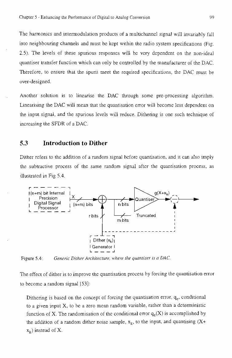
Chapter 5 - Enhancing the Performance of Digital to Analog Conversion 99
The harmonics and intermodulation products of a mititichannel signal will invariably fall
into neighbouring channels and must be kept within the radio system specifications (Fig.
2.5). The levels of these spurious responses will be very dependent on the non-ideal
quantiser transfer function which can only be controUed by the manufacturer of the DAC.
Therefore, to ensure that the spurii meet the required specifications, the DAC must be
over-designed.
Another solution is to linearise the DAC through some pre-processing algorithm.
Linearising the DAC will mean that the quantisation error wtil become less dependent on
the input signal, and the spurious levels will reduce. Dithering is one such technique of
increasing the SFDR of a DAC.
5.3 Introduction to Dither
Dither refers to the addition of a random signal before quantisation, and it can also imply
the subtractive process of the same random signal after the quantisation process, as
illustrated in Fig 5.4.
I (n+m) bit Internal I Precision I Digital Signal ' Processor
1 ' 1 I Dither (Xk) I I Generator I I I
Figure 5.4: Generic Dither Architecture, where the quantiser is a DAC.
The effect of dither is to improve the quantisation process by forcing the quantisation error
to become a random signal [53]:
Dithering is based on the concept of forcing the quantisation error, q , conditional
to a given input X, to be a zero mean random variable, rather than a deterministic
function of X. The randomisation of tiie conditional error qe(X) is accomplished by
tiie addition of a random dither noise sample, x^, to the input, and quantising (X+
Xj.) instead of X.
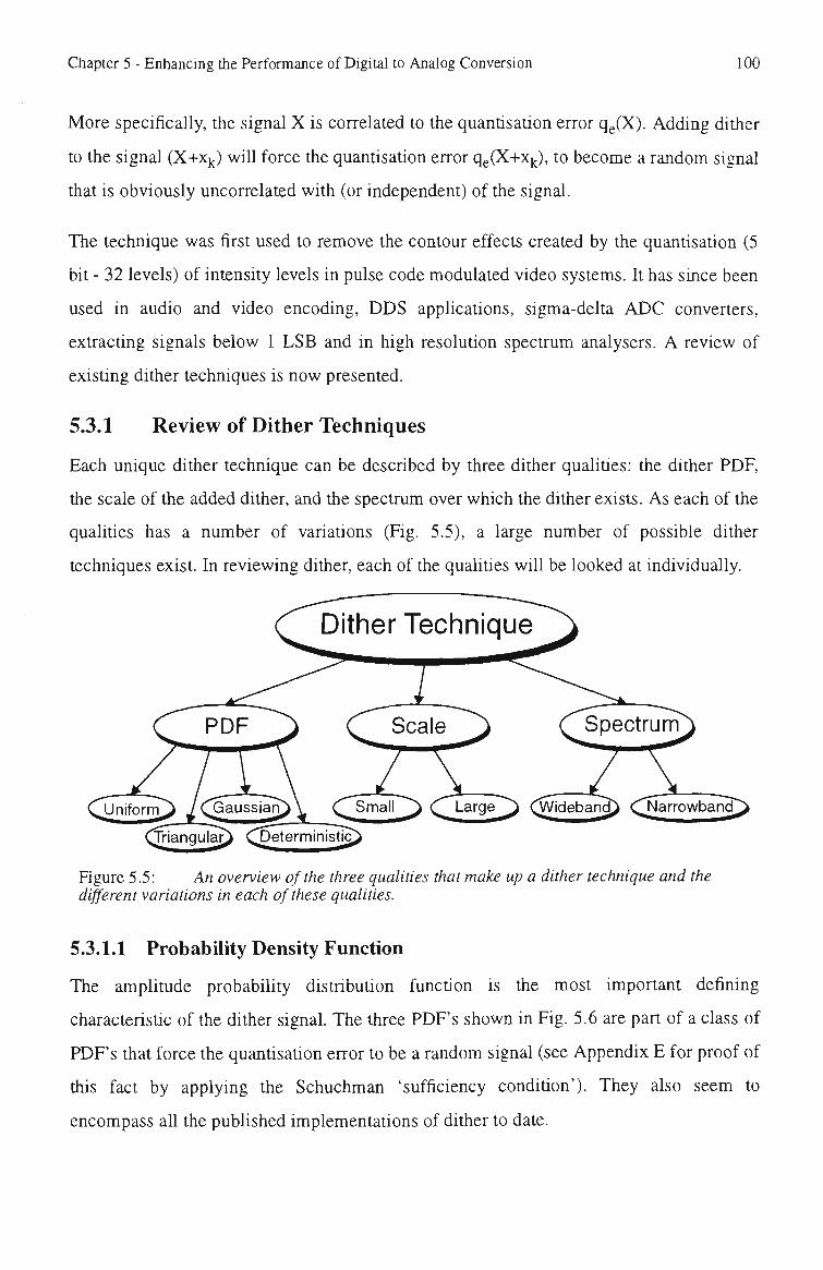
Chapter 5 - Enhancing the Performance of Digital to Analog Conversion 100
More specifically, the signal X is correlated to the quantisation error qe(X). Adding dither
to the signal (X-t-x ) witi force the quantisation error qe(X-hX]j), to become a random signal
that is obviously uncorrelated with (or independent) of the signal.
The technique was first used to remove the contour effects created by the quantisation (5
bit - 32 levels) of intensity levels in pulse code modulated video systems. It has since been
used in audio and video encoding, DDS applications, sigma-delta ADC converters,
extracting signals below 1 LSB and in high resolution spectrum analysers. A review of
existing dither techniques is now presented.
5.3.1 Review of Dither Techniques
Each unique dither technique can be described by three dither qualities: the dither PDF,
the scale of the added dither, and the spectrum over which the dither exists. As each of the
qualities has a number of variations (Fig. 5.5), a large number of possible dither
techniques exist. In reviewing dither, each of the qualities will be looked at individually.
Figure 5.5: An overview of the three qualities that make up a dither technique and the different variations in each of these qualities.
5.3.1.1 Probability Density Function
The amplitude probabihty distribution function is the most important defining
characteristic of the dither signal. The three PDF's shown in Fig. 5.6 are part of a class of
PDF's that force the quantisation error to be a random signal (see Appendix E for proof of
tills fact by applying the Schuchman 'sufficiency condition'). They also seem to
encompass aU the published implementations of dither to date.

Chapter 5 - Enhancing the Performance of Digital to Analog Conversion 101
Figure 5.6:
A PG(X) A PuW
1/c
-c/2 c/2 (a) (b) (c)
Dither probability density functions (a) Gaussian (b) Uniform (c) Triangular
The Gaussian PDF is drawn m Fig. 5.6(a), and can be described by the fotiowing equation:
ix-\if
PGM = 2a' J2n
(5.2) TTO
The power of the distribution is given by the variance cr . The mean \i is set to zero when
the DC power is zero (which is usually the case).
The Gaussian distribution was widely used in the early development of dither techniques
and is the favoured dither PDF in analogue implementations i.e. ADC dithering. This is
primarily due to the ease of generating an analogue Gaussian waveform. In a digital
implementation a large number of bits is required to accurately model the Gaussian PDF,
especially the tail region. In the simulations carried out later in this chapter, the Gaussian
PDF is truncated to -(-/- 3a. This models 97.4% of the function and is considered to be a
reasonable trade-off with the number of bits needed for accurate representation.
Dither with a uniform PDF, Fig. 5.7(b), was found to be an optimal form when the peak to
peak amplitude excursion, c, is equal to 1 LSB [55]. This only applies to quantisers with
uniform step sizes, of 1 LSB. Generation of a digital uniform PDF can be accomplished by
the simple Linear Feedback Shift Register (LFSR) technique. However, in an analogue
dithering application there are additional complications, in converting this sequence from
digital to analogue and adjusting the magnitude to exactiy 1 LSB (in the optimal case). For
digital implementations, uniform dither is a lot less complex to implement than Gaussian
dither
The Triangular PDF, Fig. 5.7(c), is generated by adding together two independent random

Chapter 5 - Enhancing the Performance of Digital to Analog Conversion 102
signals with a uniformly distributed PDF. Recentiy this has been considered to be the
optimal form of dithering [51] for audio apphcations, and is also weti suited to digital
hnplementation.
Deterministic signals, such as a sinusoid with a frequency of half the samphng rate, have
also been investigated as a possible dither source. They are not as effective as random
noise, but the combination of both random and deterministic signals can produce suntiar
benefits to optimal random noise [50].
5.3.1.2 Scale
Adding dither to the signal before quantisation is shown in Fig. 5.7(a). The output of the
quantiser, g(X-(-Xk), is written as:
g{X + x^) = (X + xj^) + q^{X + x^) (5.3)
Assuming that dither forces the quantisation error to be a random variable, tiie total noise
power is given by the sum of two independent random processes, dither, x^, and
quantisation error, qg(X-i-Xk). Thus, the dithermg system. Fig. 5.7(a), can be equivalentiy
modetied in Fig. 5.7(b). The overall error statistics of the total output noise, Wn = xj -i-
qe(X+Xjj), signal are given by [52]:
\^Wn = \^x, + \^q^ (5-4)
^k = 1 + \ (5-5)
Wn^= <5\ + <5\^ + {\i^^ + \i^f (5.6)
where fJ. and c are the mean and variance, or power, of the random signal respectively.
The subscript Xj refers to the original dither signal, q^ refers to the quantisation error, and
Wn refers to the total output noise signal. Wn^ is the total average power of the output
noise signal.
From Eqn. (5.6), the total noise power is equal to a DC term (the sum of the means
squared) and a wideband noise contribution. It is really only the wideband contribution,
Eqn. (5.6), that is important. Adding a dither signal, Xj , increases the total wideband noise
power and reduces the signal to noise ratio. The SNR can be improved by subtracting the
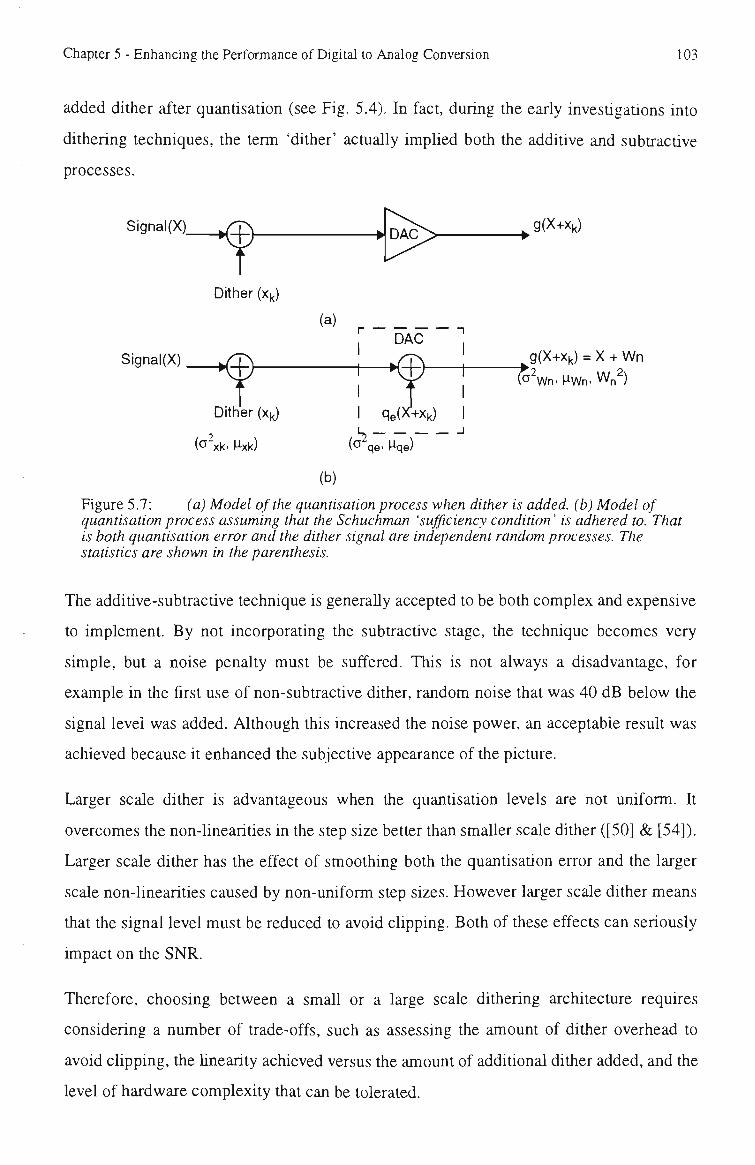
Chapter 5 - Enhancing the Performance of Digital to Analog Conversion 103
added dither after quantisation (see Fig. 5.4). In fact, during the early investigations into
dithering techniques, the term 'dither' actuaUy implied both the additive and subtractive
processes.
Slgnal(X)_
Signal(X)
^
Dither (x^)
-e
g(x+Xk)
(a) DAC
Dither (x^)
(f^^xk. ^ixk)
g(X+Xk) = X + Wn
"^^Wn. tiWn. Wn )
qe(X+Xk)
(CJ qe> Mqe)
(b)
Figure 5.7: (a) Model of the quantisation process when dither is added, (b) Model of quantisation process assuming that the Schuchman 'sufficiency condition' is adhered to. That is both quantisation error and the dither signal are independent random processes. The statistics are shown in the parenthesis.
The additive-subtractive technique is generaUy accepted to be both complex and expensive
to implement. By not incorporating the subtractive stage, the technique becomes very
simple, but a noise penalty must be suffered. This is not always a disadvantage, for
example in the first use of non-subtractive dither, random noise that was 40 dB below the
signal level was added. Although this increased the noise power, an acceptable result was
achieved because it enhanced the subjective appearance of the picture.
Larger scale dither is advantageous when the quantisation levels are not uniform. It
overcomes the non-linearities in the step size better than smaller scale dither ([50] & [54]).
Larger scale dither has the effect of smoothing both the quantisation error and the larger
scale non-linearities caused by non-uniform step sizes. However larger scale dither means
that the signal level must be reduced to avoid chpping. Both of these effects can seriously
impact on the SNR.
Therefore, choosing between a small or a large scale dithering architecture requires
considering a number of trade-offs, such as assessing the amount of dither overhead to
avoid clipping, the hnearity achieved versus the amount of additional dither added, and the
level of hardware complexity that can be tolerated.

Chapter 5 - Enhancing the Performance of Digital to Analog Conversion 104
5.3.1.3 Spectrum
Virtually ati implementations of dither simply consider adding wideband ditiier, using the
three random PDF's discussed in Section 5.3.1.1. However, Blesser and Locanthi [48]
mvestigated using a narrowband dither noise signal, Gaussian PDF, centred at tiie Nyquist
frequency in an ADC application. The bandwidtii of the ditiier signal was 1 kHz in a 22
kHz Nyquist frequency interval. In terms of spectrum, narrowband ditiier centred around
the Nyquist frequency and the wanted signal occupied mutually exclusive parts of the
spectrum.
Narrowband techniques have the disadvantage of requiring a larger amplimde dither signal
[48] to achieve the same performance. Consequently the amplitude of the signal must be
made smaller to avoid clipping. This allowance for the dither signal, called dither
overhead, reduces the SNR. A design trade-off therefore exists between the spectral width
and the required dither amplitude.
5.4 Average Quantisation Transfer Function
The average quantisation transfer function is an objective measure that will be used to
examine the effect of different dither signal properties, PDF and scale, on an arbitrary
DAC transfer function.
To calculate the average quantisation transfer function requires knowledge of only the
original quantisation transfer function, g(X), and the statistical properties, in the form of a
PDF of the dither signal. The average transfer function (averaged over all values of Xj ) can
be defined as:
g(X) = Y^g{X + x,)pix,) (5.7) k
where p{xy.) is the PDF of the dither signal, and g(X-i-Xij) is the instantaneous transfer
function of the quantiser
Equation (5.7) is equivalent to the digital convolution of the PDF and the quantiser
transfer function^ The result witi be a smoothed quantiser transfer function that
approaches the ideal linear response. Equation (5.7) can now be used as a quantitative
1. Note that the general form of convolution is ^ g(.X - x,)p(x.), but this becomes equiviiant to Eqn. (5.7) when the PDF is symmetrical about the origin. i-

Chapter 5 - Enhancing the Performance of Digital to Analog Conversion 105
means of comparing the effect of different types of dither PDF's on arbitrary quantisation
transfer functions. This objective measure consists of comparing the average quantisation
transfer function to an ideal straight fine. The closer the match, the better tiie performance.
5.4.1 The Effect of the Scale and PDF of Digital Dither on an Ideal Quantiser.
Initially, an ideal quantiser will be used to investigate the scale of digital dither on the
average transfer function, Eqn. (5.7). Uniform, triangular and Gaussian dither PDF's witi
be used in the comparisons.
For dither with either a uniform or a triangular PDF, the calculation of the average transfer
function, plotted in Fig. 5.8 (a) & (b), shows that a linear transfer function results when c
and t are equal to nA (Fig. 5.6). This is exactiy what the Schuchman 'sufficiency
condition' predicts (Appendix E). At any other peak to peak amplitude excursion of the
dither signal some deviation from linearity witi occur. For Gaussian dither. Fig. 5.8(c), an
increasingly linear average transfer function will be achieved when the scale increases.
This is also predicted by the Schuchman 'sufficiency condition'.
D.B
f 0.4 CJ
^ 0.2
'to
1 "°-2 §•-0.4
^ - O . B
-o.e
1
y y_
/T \-£
y V •
^ . 5 A
X \c=1A,2A, ...nA (linear)
0.5 1 K (LSB)
0.8
^ 0.6
I D.4
§ 0.2
.a 0 to § -0.2 I-g,-0.4
g - 0 6 < -0 .8
- 1
^ J / ^ \t=1A,2/!
(linej
y =2.5A
\, ...nA • ar)
Q 0.5 1 X (LSB)
(a) gTX) D.a
£ • 0.6 c/l
^ 0.4 g I 0.2 LL
u 0 In
e -0.2
§•-0,4
< -0,6
-0.8
• 0=0.17A yf \ A'
y /X ^ K \ o=A/2
(close to line
/ y^
=p.33A
ar)
(b)
< [LSB)
(C)
Figure 5.8: Effect of scale on the different probability distribution functions (a) Uniform (b) Triangular (c) Gaussian

Chapter 5 - Enhancing the Performance of Digital to Analog Conversion 106
The lowest scale at which linearity is achieved for uniform and triangular dither is when c
and t are equal to A. This corresponds to an increase in the wideband noise quantity of 3
dB (uniform) and 4.77 dB (triangular). For Gaussian ditiier, the Hnearity is perceptively
quite good at a = N2, or a 5 dB increase in noise power, although the 'sufficiency
condition' predicts that o should be greater than A (Appendix E). It can be concluded that
a uniform PDF forces a linear average quantisation transfer function for the lowest amount
of added dither power.
In the case of an ideal quantiser, there is no benefit in using larger scaled uniform or
triangular dither. Larger scales, which are multiples of A, increase the output noise power
but achieve no additional linearity. This is not the case when practical quantisers are
considered.
Incorrect conclusions can be drawn if Eqn. (5.7) is used alone as a quantitative measure.
For example, a uniform, c = A, and a triangular, t= A, PDF have been shown to generate a
perfectly linear average transfer function for an ideal quantiser. However, in audio
applications, an improvement in the perceptible performance of sound occurs when there
is no noise modulation [50]. In other words, the noise modulation, or second central
moment [57], must be constant across the quantisation interval:
hg{X + x,)-g{X))'\= X isi^ ^X,) -giX))"p{x,) (5.8)
= g iX)-{giX)}
It can be shown that only triangular dither satisfies this latter condition [50], and for audio
applications it is considered a better choice than uniform dither.
th The audio application suggests that all n order central moments.
E< {g{X + x,.) - g(X)) > , are potentially unportant and should be considered with the
given application in mind. However, in the context of the simple quantitative analysis that
is to follow, the first order moment is considered sufficient.

Chapter 5 - Enhancing the Performance of Digital to Analog Conversion 107
5.4.2 The Effect of the Scale and PDF of Digital Dither on a Practical
Quantiser.
A measured quantisation (DAC) error transfer function, qe(X), is shown m Fig 5.9. The
characteristic triangular quantisation error waveform, step sizes of approxiamately 1 LSB,
is a dominant feature, but there is also a major discontinmty which occurs at the point
where the DAC digital tiiput goes from negative to positive. The step size here is 2 LSB's,
constituting quite a significant non-linearity.
The average quantisation error transfer function (averaged over all values of Xj.) can be
written as:
q,{X) = X-Y^g{X-^x,)p{x,) (5.9)
and it witi replace the average quantisation transfer function, Eqn. (5.7), in this section as
the quantitative measure.
The average quantisation error transfer function, q^iX), has been calculated for uniform,
triangular and Gaussian dither, with c=A, t=A and a=A/2 respectively. These are the same
conditions as those found in the last section which make g{X) linear (or approximately
linear in the case of Gaussian); Fig 5.9(a). All the dither signals achieve a smoothing or
averaging effect on the original quantisation error transfer function.
By magnifying a small section of Fig. 5.9(a), the effects of the different dither signals can
be more closely observed, Fig. 5.9(c). Uniform dither generates a more angular curve, due
to the abrupt nature of the PDF, whereas both triangular and Gaussian dither generate
somewhat smoother curves.
The use of a larger scale dither can also remove the larger scale non-linearities, i.e. at the
point where the digital input goes from negative to positive. Figures 5.9(b) and (d)
tilustrate the effect of increasing the amplitude of the dither further. In fact, the power for
each of the different dither signals has been made to equal 4A /3 so that a fairer
comparison of the dither signals could be made. By comparing Fig. 5.9(a) and Fig. 5.9(b),
it can be seen that an increase in scale causes further smoothing of QgiX) , especially at
the point of the larger scale non-linearity.

Chapter 5 - Enhancing the Performance of Digital to Analog Conversion 108
Close examination of Fig. 5.9(b) and (d) shows that the Gaussian PDF produces a
smoother, more linear average quantisation transfer function than the other two PDF's.
This would suggest that the spurious levels would be lower in the case of Gaussian dither.
qe(X) qe(X)
(X)
-0.08
-0,09
S -0-1 w
^-0.11 o
| - 0 . 1 2
1 -0.13
i .t-0.14 •"-O.IB
-0.16
-0.17
(a)
^ \
\
Uniform ^
f -
Thanaular
A
Gaussian^ \
qe(X)
0.5
£• 0
c a
c 3 "5-0.5 a
E o
Err
or
-1.5
A-r
x'
Y,
'/ '
// \
'
-\^ \ \ i \
n \ \ / 1
/ ^
/
X (LSB)
(b)
Uniform
tiaoflulai
X(LSB)
(c)
Figure 5.9: Effect of scale on the non-uniform step size quantisation transfer function (a) Average error transfer function, q^(X) shown. Also shown is uniform (c=Aj, triangular (t=A) and Gaussian (a=A/2) dither signals added, (b) Average error transfer function, q^,(X) shown. Also shown is uniform (c=4A), triangular (t=2.82A) and Gaussian (a=l.\55A) dither signals added (Note equal power), (c) Expanded portion of (a), (d) Expanded portion of(b). Uniform dither = solid line. Triangular Dither = dash-dot line, Gaussian dither = dotted line.
In conclusion, a larger scale dither does help to overcome both the local and larger scale
non-linearities in non-uniform step size quantisers, and a Gaussian PDF also provides a
more linear average transfer function than either uniform or triangular dither. However, the
optimal dither amplitude and the corresponding amount of spurious level reduction can
only be examined accurately through measurement.

Chapter 5 - Enhancing the Performance of Digital to Analog Conversion 109
5.5 Introduction of a Novel Bandlimited Dithering Technique
Wideband dithering could be used to reduce the level of harmonic and IM products
introduced by a practical DAC. Large scale dithering wtil also be necessary (Section
5.4.2). However, a degradation in the signal to noise ratio must be endured by adding a
large scale wideband dither signal. Obviously there is a point when the increasing noise
power starts to dominate the spurious levels and at which point no further performance
gain can be made. To rectify this problem, dither could be subtracted after the DAC, Fig.
5.4, but at the expense of dramatically increasing the complexity. Instead, a novel
hnplementation of bandlimited dithering has been chosen for the multichannel
application. The bandlimited dithering technique will minimise the increase of 'in-band'
noise power when the dither signal is added, whilst at the same time reducing the spurious
level.
Implementation of bandlimited dithering also takes advantage of the multichannel signals
oversampling ratio which is required to reduce the design requirements on the
reconstruction filters following the DAC (Chapter 5). The oversampling ratio means that
there exists some frequency spectrum not being utilised by the signal. This unused
spectrum can therefore be used by the dither signal.
The novel implementation of bandlimited dithering is shown in Fig 5.10(a). The
interpolation factor chosen is dependent on oversampling ratio required to meet the
specification of a given radio system. From the conclusions of the previous chapter the
GSM and MPT1327 radio systems require an oversampling ratio of 3.2 and 5.4
respectively, which best translates to an interpolation factor of 4 for both systems.
The multichannel signal and dither spectrums are shown to be mutually exclusive in Fig.
5.10(b). A transition band is required for the digital interpolation filters and the analogue
reconstruction filters. The reconstruction filters must remove the added dither signal so
tiiat it does not cause interference in neighbouring bands. In Chapter 4, these filters were
designed for the suppression of images and not the dither power. Given that the dither
power is closer to the desired signal than are the images, then a higher order reconstruction
filter with better matching will be required.
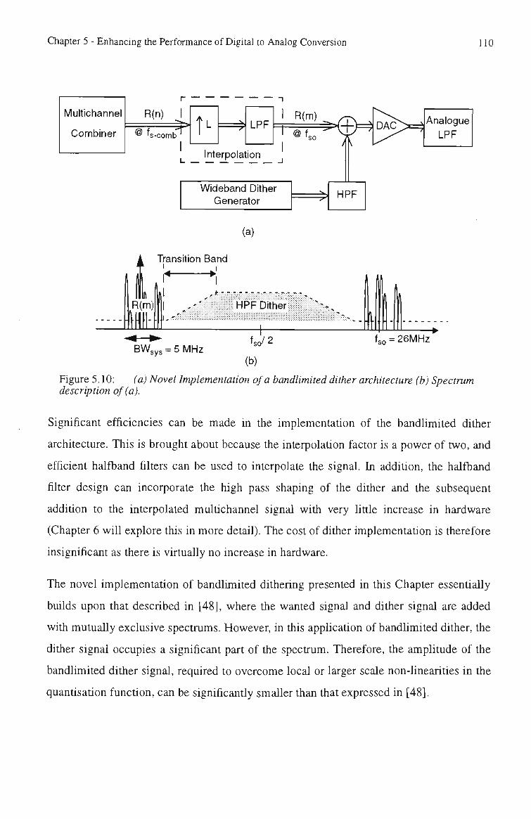
Chapter 5 - Enhancing the Performance of Digital to Analog Conversion 110
Multichannel
Combiner
R(n)
@f s-comb
I t LPF
R(m)
@f < ^ so
Interpolation 1 1 I
Wideband Dither Generator
DAC Analogue LPF
^ HPF
(a)
Transition Band
HPF Dither
A A
It BWsys = 5 MHz
W2 fso = 26MHz
(b)
Figure 5.10: (a) Novel Implementation of a bandlimited dither architecture (b) Spectrum description of (a).
Significant efficiencies can be made m the implementation of the bandlimited dither
architecture. This is brought about because the interpolation factor is a power of two, and
efficient halfband filters can be used to interpolate the signal. In addition, the halfband
filter design can incorporate the high pass shaping of the dither and the subsequent
addition to the interpolated multichannel signal with very httie increase in hardware
(Chapter 6 will explore this in more detail). The cost of dither implementation is therefore
insignificant as there is virtually no increase in hardware.
The novel implementation of bandlimited dithering presented in this Chapter essentially
builds upon that described in [48], where the wanted signal and dither signal are added
with mutually exclusive spectrums. However, in this application of bandlimited dither, the
ditiier signal occupies a significant part of the spectrum. Therefore, the amplitude of the
bandlimited dither signal, required to overcome local or larger scale non-linearities in the
quantisation function, can be significantly smaller than that expressed in [48].
Chapter 5 - Enhancing the Performance of Digital to Analog Conversion 111
5.6 Conclusion
The non-ideal transfer characteristic of the DAC interface wtil introduce signal dependent
harmonic and IM products which cannot be accurately modelled by additive white noise.
The spurious responses are important for the application of a mititichannel transmitter
because they can fall into neighbouring channels, and directly affect the overaU
performance. The use of dithering, addition of a random signal before quantisation, can be
used to minimise the spurious level.
Calculation of the average quantisation transfer fimction highlighted the favourable
properties of the dither PDF for an arbitrary quantiser transfer function. If the quantiser is
ideal, uniform dither was shown to produce a linear result for the least increase in noise
power. For a practical DAC, the average quantisation error transfer function was used to
show that the Gaussian PDF produced a smoother and more linear resitit than ditiier with a
uniform or triangular PDF, indicating lower spurious levels. Large scale dithering was also
shown to be advantageous in overcoming the local and larger scale non-linearities of a
non-ideal quantiser. This will be experimentally verified in Chapter 6.
Many different dithering techniques have been implemented with the aim of reducing the
spurious levels. The dither PDF and scale are unique in most implementations, whereas
tiie dither spectrum is wideband in ah known implementations, except for one [48].
Bandlimited dithering has been selected for the multichannel apphcation primarily to add
large scale dither whtist minimising the increase of 'in-band' noise power. The 'out-of-
band' dither noise power must be removed by higher order and better matched
reconstruction filters than that described in Chapter 4. However, the bandlimited dither can
be added with a small increase in hardware, since the filtering functions required to
spectrally shape the dither signal are already in existence.
The next Chapter will introduce the hardware implementation of bandhmited dithering,
and measurements will be used to quantify the improvement of tiie spurious free dynamic
range for larger scale dither with either a Gaussian or uniform PDF .

Chapter 6
Implementation of the Bandhmited Dithering Technique
6.1 Introduction
The analysis work in the previous chapter helped to devise a new technique, bandlimited
dithering, that can be used to lower the level of the spurious responses introduced by a
digital to analogue converter. This chapter describes the implementation of the
bandlimited dithering algorithm on both general and special purpose digital signal
processors and discusses some measured results.
The design of the halfband interpolators and the dither generator used in the bandlimited
algorithm are described in Section 6.2. These designs were then implemented in hardware
using a general purpose DSP, which was subsequently used to obtain measured results in a
multichannel system. The results in Section 6.3 show that bandlimited dithering reduces
the spurious levels generated by the DAC, producing between 2 and 4 dB improvement in
performance. It is shown that large scale dither is necessary to produce these positive
results and for this reason, the use of wideband dithering techniques is impractical because
of the large increase in the in-band noise floor.
The low sampling frequency achieved using a general purpose DSP was a major
limitation. Section 6.4 describes a special purpose DSP (ASIC) that was designed to
obtain sampling frequencies which are a factor of 100 times faster than the general
purpose DSP.
112

Chapter 6 - Implementation of the Bandlimited Dithering Technique 113
6.2 Bandlimited Dithering Architecture
The bandlimited dithering architecture adds the dither signal to the multichannel signal
during the interpolation process. Fig. 6.1. The architecture consists of two halfband filter
stages which achieve an overall interpolation factor of 4. This was found to be an adequate
value for overcoming a 5% mismatch in the reconstruction filters used in analogue direct
upconversion (Chapter 4). Note that dither is only added in the second stage of
interpolation to ease the analogue reconstruction filter requirements.
^comb
Channels/
1.5 5
Digital Signal Processing
Stage 1
• t2 t2
"A ^ :i
Stage 2
t2 t2
" \
^
Q S o fc-
I IT
analogue Direct Upconverter
cos Wopt
n - •n i^»
T, sin Wjyjt
.J
Figure 6.1: The bandlimited dithering architecture.
The next two sections witi examine the design of the halfband interpolators and the dither
generator.
6.2.1 Design of the Interpolator
The multichannel signal is interpolated by a halfband filter (Appendix B.2) with a lowpass
spectral shape of HLPF(f), whilst the added wideband dither signal is required to be
spectrally shaped by a filter with the opposite frequency specifications. The dither filter
(highpass) parameters are derived from the lowpass parameters as follows:
fstop-HPF - fpass-LPF
fpass-HPF = fstop-LPF
(6.1)
Note that the stopband, 6^, and passband, 5p, ripple specifications for botii filters are equal.
The resulting frequency response for the HPF has the same shape as that of the lowpass
filter but it is frequency translated by half the sampling frequency:
HHPF(f)=HLPF(fs/2-f) (6.2)

Chapter 6 - Implementation of the Bandlimited Dithering Technique 114
The coefficients of the HPF required to shape the dither signal can now be directiy
obtained from the LPF by changing the sign of every second coefficient:
n+l hHPF(n) = (-1)""^. hLPF(n) (6.3)
For a halfband filter the transformation is trivial because the even coefficients are all zero,
except for the centre tap which is simply negated. Each halfband interpolator stage can
then be drawn as shown in Fig. 6.2(a), where the multichannel signal is interpolated,
R(m), by a standard halfband architecture (Appendix B.2) before being added to the
spectrally shaped dither signal, d(m).
R(n)-r-EHi3T-|i3-li3
d(n)-r-EHi3-riiHi3--R(m) + d(m)
z : ) — •
(a)
R(m) -h d(m)
(b) Figure 6.2: (a) Interpolation half-band stage. Addition of the interpolated multichannel signal and the highpass filtered dither signal (b) Optimised architecture of (a)
The filter required to spectrally shape the dither signal is identical to the interpolator,
except tiiat the centre tap, h^tap. is negated. The two filters in Fig. 6.2(a) can therefore be
easily merged to form a highly efficient architecture as shown in Fig. 6.2(b). Note that
each delay shown, z'^ is simply implemented as a register clocked at the output sampling

Chapter 6 - Implementation of the Bandlimited Dithering Technique 115
frequency. Two registers of this type can be combined together into a single register which
is clocked at the lower input sampUng frequency. Compared to the original interpolator,
only two more adders and a delay line (shown shaded in Fig. 6.2(b)) are needed to carry
out the additional dithering tasks. Thus the benefits of bandlimited dithering can be
obtained for very httle increase in circuitry.
The spectral interpretation of the interpolation process is iUustrated in Fig. 6.3. The
original baseband multichannel signal has a system bandwidth of 5 MHz (BW^y ) and is
sampled at 6.5 MHz (fs-comb)' Fig- 6.3(a). After the first interpolation stage, the output
consists of the multichannel signal interpolated by a factor of 2, Fig. 6.3(b). The second
stage interpolates this entire signal and adds an amount of bandlimited dither, as shown m
Fig. 6.3(c). The difference between the two interpolator stages is that the filtering
requirements are less stringent for the second stage.
Afr
h«\ll-#i-i----m-.-f'-.M4-i.-.-^^sys s-comb
Afj =8 MHz
h&r'----iA:i
fk' 1 4§!kA
i nn—d
Uither •<•• I I I ••••
(C) so
Figure 6.3: (a) Multichannel signal, BW^y^ = 5MHz, sampled atfj-.^omb = 6.5MHz. The first stage interpolation filter spectral shape is shown dotted, (b) Spectral interpretation at the output of the first stage interpolation filter The second stage interpolation filter spectral shape is shown dotted, (c) Spectral interpretation at the output of the second stage interpolation filter
Overall the architecture adds 2.5 MHz of dither with a transition width of approxiamately
8 MHz. This added dither signal has to be removed by the reconstruction filters.

Chapter 6 - Implementation of the Bandlimited Dithering Technique 116
6.2.2 PDF Selection for the Dither Generator
The dither source is a random number generator with a given PDF. Selection of the PDF
used in the dither generator is based on two criteria, ease of implementation and
performance.
The dither PDF must be simple to implement in a digital environment. The uniform PDF
is better suited and less complex m a digital implementation than the Gaussian PDF, given
that only a Gaussian and a uniform PDF are considered.
Selection of the PDF based on peri'ormance is not as simple. The previous chapter used the
average quantisation transfer function, Eqn. (5.7), to compare the effect of different dither
PDF's on a practical DAC transfer characteristic. The analysis indicated that a Gaussian
PDF would perform shghtiy better than the uniform PDF. The remainder of this section
uses measurement to quantify the performance of different PDF's in the bandlimited
architecture.
Three dither sources, one with Gaussian and two with uniform PDF's, Table 6.1, are tested
using the hardware described in Appendix F. The difference between the two uniform
sources is the DC bias of the dither generator. In all cases the dither is wideband before it
is shaped and added to the interpolated signal.
Table 6.1: Definition of the bandlimited dithering sources
PDF of tiie dither source
Gaussian
Uniform
Uniform
DC bias of the dither source
NO
NO
YES"
Terminology used in text
Gaussian Bandlimited dithering
Uniform bandlimited dithering
Uniform bandlimited dithering with bias
a. Refers to the input dither source having a finite statistical mean. b. The input dither source has a statistical mean is equal to c/2.
The measurements are based around the operation of a 9 bit DAC, primarily due to the
dynamic range limitations of the spectrum analyser used. A higher precision DAC could
be measured if notch filters are used to eliminate the main signals and low noise amphfiers
are used to enhance the intermodulation products. However, both of these techniques
would increase the complexity of the measurements and have the potential to further

Chapter 6 - Implementation of the Bandlimited Dithering Technique 117
distort the output. The measurements wtil highlight the benefits and disadvantages of the
different dithering techniques that would be equally apphcable to a higher precision DAC.
The 9 bit DAC used is quite nonlinear, as iUustrated via the DAC quantisation error
transfer function, qe(X) in Fig. 6.4(a). The peak to peak error is ahnost 3A, in contrast to
an ideal DAC where qe(X) would be uniformly distributed between -A/2 and A/2 (peak to
peak error of A), Fig. 5.1(c).
qe(X) » • • OW: 7 3 HX. VSW; Oft D: SWEPT gPECTBUM MKr-
H '.a . n.4 S a t
,
" I ' i " '
- SFDR - ." ^HRr T r 1
V,, 11.. 1 . . Ii * ^ -
MJ'^S^IWUN
1
OvX/l^ »J*Vll »J> JU» J V T V 4 V ' ^ V T rfv^lu/<
. -100 0 100
Digital Input (LSB)
8CaP"t.: o Hx. AVERAOZMO AVO: U
Ctoo- SO OOO
(a) (b) Figure 6.4: (a) 9 bit DAC quantisation error transfer function, qg(X). (b) The DAC output spectrum of a sinusoid with no dither added.
The different dither sources will be compared using a single tone generated in a lookup
table, with the signal frequency set to an integer multiple of the samphng frequency.
Although the signal is not what would be typically encountered, it does highhght the
beneficial effects of dithering. The DAC output spectrum of the mterpolated tone with no
dither added is shown in Fig. 6.4(b), where tiie quantisation noise is concentrated into
harmonics of the original signal, resulting in an SFDR of 33 dBc.
The effect of increasing the power of the different dither sources is shown in Fig. 6.5(a).
The signal amplitude has a constant 7 bit full scale amplitude whilst the dither amphtude
is increased. For all dither signals, the worst spurious level is shown to decrease when the
dither power is increased i.e. the SFDR increases. The measurements show that uniform
and Gaussian bandlimited dithering, i.e. sources with no DC bias, perform very similarly.
However, a performance increase of l->2dB is observed for the uniform bandlimited
dithering with bias technique. Fig. 6.5(a). The difference in performance can be attributed
to PDF of the bandlimited dither added and the DC offset of the dither source.
1. All measurements were performed on the 9 least significant bits of a 16 bit DAC device..

Chapter 6 - Implementation of the Bandlimited Dithering Technique 118
45
| 4 0
a LL
35
3D
/ /
/ /
, 7
^ ^ /
• ^^"^ ~ ! I ^ ' ^ - r : ^ — - -
SFDR-no dither added
•
a.5
0.45
0.4
0.35
0.3
Q 0 25
0.2
0.15
0.1
0.05
10 10-^ 10-'
Uniform
Uniform bandlimited / with bias i i
f
/ W ^ bandlimited .' / N •" Gaussian / \<^r^and limited
\
\
10 10 Dither Scale (LSB)
-4 - 2 - 1 0 1 amplitude (LSB)
(a) (b)
Figure 6.5: Plot of SFDR versus power of the added dither signal.(a) Uniform bandlimited dithering '....', Uniform bandlimited dithering with bias '.-.-.-', Gaussian bandlimited dithering- solid (b) PDF's of the bandlimited dither added before quantisation. Power is normalised to A .
If the ditiier source into the halfband shaping filter is Gaussian then the PDF of the
bandlimited dither added to the upconverted signal wiU also be Gaussian, Fig. 6.5(b).
Further, when the dither source is uniformly distributed, with no DC bias, then the
resulting PDF also has a shape simtiar to Gaussian, Fig. 6.5(b). Both of these dither
sources have a similar level of measured performance, as would be predicted through the
calculation of the average quantisation transfer function. However, if the source is
uniformly distributed, with a DC bias, then the PDF is a combination of a uniform
distribution, in the negative region, and a Gaussian PDF, in the positive region. Fig. 6.5(b).
This PDF gives a greater probability of large dither amplitudes than the other two
schemes.
The DC offset of the dither PDF source also generates a sinusoid at half the sampling rate
(see Fig. 6.7(b)). The combination of a random dither signal with a sinusoid at half the
sampling frequency has been reported to result in an improved performance [50]. This
situation has also been observed here.
Based upon the ease of implementation and measured performance, the dither source has
been selected to be uniformly distributed with a DC bias of c/2.

Chapter 6 - Implementation of the Bandlimited Dithering Technique 119
6.3 Bandlimited Dithering Results
This section presents the measured results of bandhmited dithering in a multichannel
system. A scaled version of the GSM radio system has been implemented due to the
sampling rate limitations of the development system. Figure 6.6 shows the fitil GSM
system frequencies and the corresponding scaled system frequencies.
A Second stage Interpolating filter
13 MHz-Full GSM system 47.5 kHz - Scaled system
2.5 MHz-Full GSM system
9.13 kHz - Scaled system
Figure 6.6: Graphical illustration of the frequencies required for a full GSM system with a system bandwidth of 5MHz and the corresponding scaled GSM system used in measurements.
Equation (3.32) predicts that the CNR^^jfj at the output of the quadrature upconverter will
be 73.26 dBc, assuming that 4 channels are combined and that both 9 bit DAC's are ideal.
This is more than sufficient for a GSM transmitter with a power class of 8 (TRX8), which
requires a CNRj uiti of 70dBc. However, the DAC is not ideal, as shown in Fig. 6.4(a), and
the performance will be lower than predicted.
The effect of the non-ideal DAC is demonstrated m Fig. 6.7(a), where four channels are
activated within the system bandwidth. The output spectrum from the DAC shows many
spurious responses occurring across the Nyquist bandwidth. Only the spurious responses
that fall in-band or close to the edges of the system bandwidth are considered in the
calculation of the SFDR. The other spurii wtil be ehminated by tiie subsequent filters. The
calculated SFDR is therefore 47dBc, a massive 23dB less than the 70dBc system
specification.

Chapter 6 - Implementation of the Bandhmited Dithering Technique 120
Hmnom: -20 dBm Ovar«w«ap; o f f 13-Oct- loao 13- o i R«» aw; SB H2 VBH: Off 3wp Tim.; 77. ea Sec B:SHEPT SPECTRUM MKP 2 las MZ - 3 2 . 8 6 OBm
-SO
LogMag
Rang*: -SO aBm Ovarawsap: Off n«a BW: 36 Hx VBM; Off B: SWEPT SPECTRUM M<r
-SO
- 1 2 0 dBm
u '^^ rWVV*
i3-oct-iBas 13! ae SwD Tiwm. T 7 . a 2 ^ c
15= Hr - 3 9 . O H eieiB
iJso/2
SFDR = 53 dBc
v X v ^
z:
^dutoreand ' iSSS
Centar: 23 000 HZ AVERAGZNa Ave: 10
Span: 50 000 Hz Canaan 25 OOO Hz AVERASINO AVG: 9
Span: 60 OOO HZ
(a) (b)
Figure 6.7: (a) Scaled GSM system with no dither added, f^g = 95kHz (b) Scaled GSM system with bandlimited dither added.
The level of the spurious responses can be reduced through the addition of bandlimited
dithering, as is tilustrated in Fig. 6.7(b), where the SFDR has been increased to 53 dBc.
The dither is also shown to be added 'out of band', and so it will not affect the in-band
noise floor. The DC offset of the dither PDF source has also generated a sinusoid al half
the sampling rate. Fig 6.7(b).
The effect of dither power (amplitude) on the SFDR is shown in Fig. 6.8(a). The SFDR
only improves when there is at least lOOA^ of dither power, highhghting the benefit of
larger scale dither on the spurious levels. Note, that as the dither level was increased, the
carrier level was reduced so that the sum of the two signals did not exceed the 9 bit full
scale range of the DAC. hi other words, no chpping was allowed to occur.
The carrier to noise ratio uses a noise measurement bandwidth of BW meas'
As the dither
level increases, the carrier power decreases, whilst the in-band noise floor remains
approximately constant. The carrier to noise ratio witi therefore decrease as shown in Fig
6.8(b). The reduction is substantial at high dither levels.
An ideal DAC has a CNR of 73.3 dBc (dash-dot line on Fig. 6.8(b)) which is substantially
better than the measured DAC, even witii no ditiier added. This is due to the poor
quantisation error of the measured DAC (peak to peak error is 2.6A in Fig 6.4(a), and this
explains the 7 dB of additional quantisation noise.

Chapter 6 - Implementation of the Bandhmited Dithering Technique 121
10 IQ' 10 ' 10" Dither Power (LSB squared)
(a)
I'z
70
BE
" 6 0 CQ -E3
a: g5B
50
45
10
_ - -^ 7dB '
- 1 10°
1 10 l o ' 10
-
-
\ -
\
\.
10 Dither Power (LSE sqiiared)
(b)
Figure 6.8: (a) Plot of the SFDR vs. the Dither power The SFDR when no dither is added isshown '....'. (b) Plot of CNR versus Dither Power The ideal CNR^ulti for a 9 bit DAC when 4 channels are activated is shown '-.-.-.'.
The CNR and the SFDR can now be combined into a quantity called the Carrier to Noise
and Distortion ratio (CaNAD), where the distortion power is the sum of the noise (CNR)
and spurious power (SFDR) measured within a bandwidth of EWj gag. The carrier to noise
and distortion ratio of the worst channel is defined as:
CaNAD = (SFDR-i + CNR"^)'^ (6.4)
where the SFDR and CNR are expressed as linear power ratios, not in decibels.
The CaNAD has been plotted in Fig. 6.9(a), shown with a dashed line. The SFDR
dominates the CNR for small values of dither power, whilst the reverse is true for larger
values of dither power. The resulting CaNAD therefore arrives at an optimum value of 50
dBc when the SFDR and CNR are approxiamately equal. Although the addition of
bandlunited dither resulted in a 2 dB improvement, the level of improvement is sttil not
enough to meet the GSM CNRj uiti system specification of 70 dBc.
Dither power equal to 2000A^ or a dither amplitude equal to half of the 9 bit full scale
range of the DAC is required to achieve this 2 dB of improvement. Therefore, large scale
dither is necessary to overcome nonlinearity in a practical DAC. Small scale dither
(amplitude variation is the order of 1 LSB) has no affect on performance.

Chapter 6 - Implementation of the Bandlimited Dithering Technique ] T 0
u BO
10 10 10 ' 10 ' Dither Power (LSB squared)
10 1C' 10" 10" Dither Pcwer (LSB squared)
(a) (b)
Figure 6.9: (a) The effect of adding bandlimited dither The CaNAD is shown dotted, (b) The effect of adding wideband dither The CaNAD is shown '---'. The SFDR when no dither is added is shown '....'and the ideal CNR^nuitifor a 9 bit DAC when 4 channels are activated is shown '.-.-.-'.
6.3.1 Wideband Dither
One of the main advantages of bandlimited dither over wideband dither is that the dither
power is added out of band. The addition of wideband dither increases the in-band noise
power and causes the CNR curve to decrease at a much faster rate. This is illustrated in
Fig. 6.9(b), where the CNR curve dominates the SFDR curve before any enhancements in
the level of the spuriouses can be made. Adding wideband dither for this application
therefore provides no benefits unless the added dither can be successfully subtracted after
tiie DAC.
6.3.2 DC Offset Effect
The perforaiance of bandhmited dithering was found to be enhanced by removing the DC
offset from the DAC transfer characteristic.
It was noticed that the odd harmonics or intermodulation products dominated for small
amounts of dither. This can be attributed to the odd order transfer characteristic of the
DAC, Fig. 6.10(a). However, the even harmonics became more significant as the dither
power increased and dominated at the point of optimal performance. It is well known that
even harmonics and intermodulation products can be generated from a third order transfer
characteristic if a DC offset exists. The DAC transfer characteristic has a DC offset of 34
LSBs, Fig. 6.10(a).

Chapter 6 - Implementation of the Bandhmited Dithering Technique 12.-
.
CNR
SFDR
•
- ^ . ^ ^ ^ ^
Y-4dBj
Analogue Output (mv) IQ 10 Dither Power (LSE squared)
(a) (b)
Figure 6.10: (a) DAC transfer function (b) The effect of adding bandlimited dither with DC offset removed. The CaNAD is shown '—'. The SFDR when no dither is added is shown '...' and the ideal CNRffi^ififor a 9 bit DAC when 4 channels are activated is shown '-.-.-.'.
When the DC offset was removed the even harmonics were no longer dominant at the
point of optimal performance and the SFDR was subsequently enhanced. The optimal
point of the CaNAD curve has now increased to 4 dB, Fig. 6.10(b).
6.3.3 An Ideal DAC
The effect of bandlimited dither on a close-to-ideal DAC was also measured by using the 9
MSBs of a 16 bit DAC, as opposed to the 9 LSBs. As expected, the measured quantisation
noise, CNR, was within 1 dB of the ideal value. Fig. 6.11.
10 10 10' 10^ Dither Power (LSB squarefl)
(a)
Figure 6.11: The effect of adding bandlimited dither for a close-to-ideal DAC. The CaNAD is shown ' '. The ideal CNR^^ifJor a 9 bit DAC when 4 channels are activated is shown

Chapter 6 - Implementation of the Bandhmited Dithering Technique 124
The worst spurious response for the close-to-ideal 9 bit DAC was 20 dB better than for the
practical 9 bit DAC measured previously, and when dither was added the spurious
responses decreased. However, the SFDR remained constant because tiie signal level also
decreased. Additionally, the CNR decreases and dominates the CaNAD equation almost
unmediately. The result is that no gain in performance is observed by adding bandlimited
dithering for a DAC with a close-to-ideal transfer function.
6.3.4 Dithering Remarks
The measurements have shown that adding large scale bandlimited dither to the
multichannel signal improves the performance of the DAC, whilst small scale dither has
no affect on performance of the practical DAC. The larger scale bandhmited dither wtil
place a more stringent requirement on the reconstruction filters discussed in Chapter 4,
because the dither signal is closer to the desired signal than are the images. Higher order
filters with better matching will be required.
Conventional wideband dithering provides no benefit for the multichannel base station
apphcation. This is because the large scale dither, that is required to overcome the non-
linearity of the DAC, causes the in-band noise floor to dominate the CaNAD before any
improvement in the spurious level can be made. Similarly, dithering of any form will not
enhance the performance of the DAC, for a close-to-ideal DAC.
6.4 The Bandlimited Dithering ASIC
One of the major limitations of the C40 digital signal processing development system was
tiie maximum sampling rate. The large number of instructions required to implement the
second stage mterpolator and dither generator meant that the output sampling frequency
was hmited to 95 kHz, a lot lower than tiie output samphng frequency of 26 MHz required
for a GSM system with a 5 MHz system bandwidth. This section describes an Application
Specific Integrated Circuit (ASIC), whose main purpose is the increase of the output
sampling speed, Fig 6.12.
Two separate ASIC's were designed for tiie In Phase and Quadrature channels. Both have
tiie same architecture, except for the uniform random number generators, which must be
independent. The output sampling frequency is set by an external clock which also drives
tiie DAC's.

Chapter 6 - Implementation of the Bandlimited Dithering Technique 12.
OT o Q. . 3
a. 1 c 0 O
Q
Reset
Clk@
Uniform Random Number Generator
*
fso/2
16
T
0} 3= 3
CQ
3 a c
Q ^^/\
R(n)
Second stage
Interpolator
d(n)
t2
17.
t2 AM 2 H T ^ ^ I I W I o O
Clock @ f so
0 3 3
o
17^
Same Architecture as above
Figure 6.12: Position of the bandlimited dithering ASIC, the main connections and the schematic of the architecture contained within the ASIC
The interface to the preceding DSP is simple and requires no additional circuitry. The
ASIC generates a clock signal at the input sampling frequency, fso/2. This enables the
synchronous transfer of 16 bit twos complement data into the input buffer of the ASIC. A
reset pulse can be initiated by the DSP to ensure that the uniform random number
generators are operating independently on both the In Phase and Quadrature ASIC's.
Two auxiliary functions, dither scaling and configuration of the output data, are also
included in the ASIC. The scaling of the 8 bit dither word is required for optimising the
performance of the DAC, whilst the output data can be configured as either a twos
complement or a binary number.
The architecture of the halfband interpolator and dither generator will now be discussed in
Sections 6.4.1 and 6.4.2 respectively.

Chapter 6 - Implementation of the Bandlimited Dithering Technique 126
6.4.1 Halfband Interpolator Design
The frequency response for the halfband filter is shown in Fig. 6.13.
-20
5
-60
-120 4 6 -
Frequency (MHz)
Figure 6.13: Frequency response for the halfband interpolator
The second stage halfband interpolator has been designed for a stopband attenuation of 90
dB, so that it can be used for either the GSM or MPT1327 radio systems. The passband
and stopband frequencies are set at 2.84 MHz and 10.16 MHz respectively, when the
output samphng frequency is 26 MHz. The Parks McClellan equiripple algorithm was
used to calculate the 17 bit twos complement filter coefficients from these specifications.
Table 6.2. Note that the even coefficients are ati zero except for the centre tap, h 12-
Table 6.2: Filter Coefficients for the Halfband Interpolator
Coefficient
hi
h3
h5
h7
h9
hll
hj2
Twcs Complement
1 n i l 1111 1111 0010(-14)
0 0000 0000 0111 1110(126)
1 1111 1101 1100 0110 (-570)
000000111 0011 1110(1854)
1 1110 1011 1001 0100 (-5228)
0 01001110 1111 1001 (20217)
0 1000 0000 0000 0000 (32768)
Equivalent Signed Binary
- 1110
111 1110
-100011 1010
111 0011 1110
-1 0100 0110 1100
101 1110 1111 1001
1000 0000 0000 0000
CSD
(-1)0010
1000 00(-1)0
(-1)0 0(-l)00 Olio
100(-1)0100 00(-1)0
(-1)0(-1)00 (-1)001 0100
0101 000(-l)0000 100(-l)
Not Used
The hardware efficient shift and add technique was used to implement the multiphcation
of each coefficient. The coefficients are most efficientiy implemented using the Canonical
Signed Digit (CSD) representation for signed binary numbers. Each binary digit can take
one of three possible values; 4-1, 0 ,-1. The result of converting a given coefficient into
CSD representation is the reduction in the number of 1 's and therefore the number of shift

Chapter 6 - Implementation of the Bandlimited Dithering Technique 127
and adds reqttired to complete the multiphcation. This can be verified by examination of
Table 6.2. The centre tap, h-^j, wtil require oitiy a simple shift right operation (divide by
two).
The architecture of the halfband interpolator is shown in Fig. 6.14; this was derived earlier
in Fig. 6.2(b). All arithmetic operations occur at the input sampling frequency, whilst only
the switch is clocked at the output sampUng frequency. To ensure fast operation,
pipehning of the data has been used, the result is a latency of 10 clock cycles or 0.385us at
an output sampling frequency of 26 MHz.
The halfband filter has been implemented using full precision arithmetic. This means that
all filter calculations have been completed at futi precision until the last summation stage
which truncates the result to 17 bits. This ensures that a build up in quantisation noise wtil
not occur.
R(n)-:J4->®
d ( n ) - 7 ^ A ^ ^^^'17^^R(m)-hd(m)
Figure 6.14: Halfband interpolator architecture with dither shaping incorporated, as implemented in the ASIC
The increase in circuitry for the hah"band interpolator with dither shaping compared to a
standard halfband interpolator, is very small. Only an extra two adders and 5 delay
elements are required (shown shaded in Fig. 6.14). In the final layout of the ASIC, the
additional circuitry represents only 2.5% of the total die area.
6.4.2 Uniform Dither Generator
The uniform dither generator implementation is based on tiie Linear Feedback Shift
Register (LFSR) technique. However, tiie LFSR must generate a word rather tiian tiie
normal serial bit stream. The generation of m-sequences as a series of non-overlapping W
bit words is discussed in [58], and the same technique has been applied directiy to this
apphcation.

Chapter 6 - Implementation of the Bandlimited Dithering Technique 128
The precision of the dither has been selected to equal just the integer quantity reqttired.
The reason for this is that the fractional quantity of dither (small scale) did not enhance the
performance of a practical DAC. From the measurements of a 9 bit DAC, the optimum
scale of the dither occurred at approximately half the 9 bit fuU scale range, or 8 integer
bits. A facility exists to scale the 8 bit dither word.
For the generator to closely approximate white noise, the m-sequence length has been set
to 2 - 1 . The feedback taps have been derived from the characteristic polynomial for the
LFSR as 0 and 3 for N=25 [59]. The technique described in [58] is used to ensure that
each of the 8 bit streams is shifted from one another by 2^^/ 8 = 4*10^ bits. A sufficientiy
large shift is necessary to ensure that the 8 bit word closely approximates white noise. The
schematic of the dither generator is shown in Fig. 6.15.
Figure 6.15: 25 stage LFSR 8 bit word generator
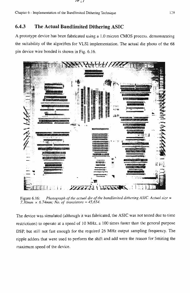
/<r j /
Chapter 6 - Implementation of the Bandlimited Dithering Technique 129
6.4.3 The Actual Bandlimited Dithering ASIC
A prototype device has been fabricated using a 1.0 micron CMOS process, demonstrating
the suitability of the algorithm for VLSI implementation. The acmal die photo of the 68
pin device wire bonded is shown in Fig. 6.16.
Figure 6.16: Photograph of the actual die of the bandlimited dithering ASIC. Actual size 7.30mm x 6.74mm; No. of transistors = 45,654.
The device was simulated (although it was fabricated, the ASIC was not tested due to time
restrictions) to operate at a speed of 10 MHz, a 100 times faster than the general purpose
DSP, but still not fast enough for the required 26 MHz output sampling frequency. The
ripple adders that were used to perform the shift and add were the reason for limiting the
maximum speed of the device.

Chapter 6 - Implementation of the Bandhmited Dithering Technique 130
6.5 Conclusion
The performance of the bandhntited dithering technique was measured by tiie carrier to
noise and distortion ratio (CaNAD). The distortion was obtamed by the spurious free
dynamic range (SFDR) and the carrier to noise ratio (CNR), where the noise was
measured in a bandwidtii of BW^eas- The CaNAD of a practical DAC is dominated by tiie
spurious levels, which reduce when bandlimited dither is added. To avoid chppmg, tiie
carrier level must be reduced as the dither level is increased, which subsequentiy reduces
the CNR. The CNR then becomes dominant at large dither levels. An optimal CaNAD
performance occurs when the SFDR and CNR quantities are approximately equal. For the
9 bit DAC measured in this chapter, a 2 to 4 dB increase in performance was found when
the peak to peak dither amplitude covered half the full scale range of the DAC.
The scale of dither requh-ed to produce optimal performance wtil be very dependent on the
DAC transfer function. The DAC tested had quite a significant amount of nonhnearity
which required the addition of a large scale bandlimited ditiier to enhance its performance.
Wideband dither was shown to provide no benefit because it produced a large increase in
the in-band noise floor. In addition, dithering gave no improvement in performance if there
was no step nonlinearity in the DAC characteristic (close-to-ideal DAC). Practical DAC's
do not usually fall into this category.
The hardware implementation of the bandhmited dithering technique was also described.
Central to the technique was found to be the interpolation by a factor 4 required to
overcome a 5% mismatch in the reconstruction filters. Two interpolate by 2 stages were
used to reduce the processing load. The design of an ASIC for the second and higher
sampling frequency stage was implemented. It consisted of a halfband interpolator and a
dither generator.
The halfband interpolator increases the sampling rate of the multichannel signal by 2 and
also performs the shaping of the wideband dither so that the signal and dither spectrums
are mutually exclusive. The architecture requires an extra two adders and 5 delay elements
compared to the standard halfband interpolator. The extra circuitry represents only 2.5%
of the total die area of the fabricated ASIC.
The dither generator produced a uniformly distributed random number with a DC bias.

Chapter 6 - Implementation of the Bandlimited Dithering Technique 131
This performed better than the other PDF's that were considered and was simply
implemented in hardware usuig the LFSR technique. Only 0.9% of the total die area was
used for this function.
A special purpose DSP was butit to demonstrate the suitability of the algoritiim for
integrated circuit implementation and to improve upon the low sampling speed of the
general purpose DSP. The ASIC design increased the samphng speed by a factor of 100
(to 10 MHz), StiU short of the 26 MHz required. The ripple adders restricted the maximum
sampling rate, which could be increased by relaxing of the attenuation specification (to
account for the roll-off of the reconstruction filters), modifying the halfband canonical
transversal filter architecture to the modified transversal filter architecture, reducing the
coefficient wordlength, utilising a more advanced silicon technology and ceti library
(including carry lookahead adders) and introducing more pipeling into the design. The 26
MHz sampling speed required for implementing a system bandwidth of 5 MHz should
then become achievable.
Bandlimited dithering technique improves the effective DAC precision by approximately
half a bit. This improvement has been achieved for a very small increase in hardware.
However, because the dither signal is closer to the desired signal than are the images,
higher order and better matched reconstruction filters than those discussed in chapter 4
wtil be required.

Chapter 7
Conclusion
The thesis has focused on a new multichannel transmitter architecture suitable for current
and future radio communication systems. This novel technique has involved combinmg
the channels at low power levels in a digital signal processor before being amplified by a
wideband ultra-linear amplifier. This thesis has concentrated on the pre-amplifier stages,
that is the low power channel combiner, the digital to analogue converter and the
frequency upconverter.
Existing radio base stations use a separate modulator and power amplifier for each
channel. The channels are then combined at RF, using expensive, precision made cavity
resonators and ferrite isolators, prior to feeding the antenna. Chapter 2 reviewed these
main components in detail and showed that the cavity resonators restrict the minimum
channel separation and require mechanical adjustment, when retuned to a new transmit
frequency. They are responsible for the high cost, large bulk and low flexibtiity of current
base station architectures. Introduction of the low power combining architecture
highlighted that the cavity resonator was not needed, and therefore, a reduction in size and
cost of the base station could be achieved. In addition, combining the channels in a DSP
environment did not limit the frequency agility or the total number of transmitted
channels. The DSP architecture is extremely flexible because the entire functionality of
the base station, i.e. modulation format, power control, and channel frequency allocation,
can be software programmable.
132

Chapter 7 - Conclusion 133
Chapter 2 has also identified four design challenges of the new DSP low power combining
architecture:
• multichannel combining,
• frequency conversion to RF,
• DAC interface and
• the wideband ultra-linear power amplifier.
The thesis considered the first three challenges.
The multichannel combining algorithm is made up of an interpolator, multiplier and
summer. Chapter 3 investigated three efficient interpolator techniques to minimise the
computational load for practical implementation and power consumption reasons. The
LUT approach was found to be the most efficient but it is only suitable for digital
modulation schemes, where the number of output states (trajectories) is small enough not
to require an excessive amount of memory. In contrast, the cascaded halfband approach
was shown to be suitable for both analogue and digital modulations at the expense of a
larger computational load. A third algorithm, the polyphase FFT technique, was
introduced as an efficient algorithm for combining a large number of channels. It was
found to be more efficient than the cascaded halfband approach when more than 8
channels were combined.
Chapter 3 also investigated and compared four frequency upconversion techniques which
translate the baseband multichannel signal to RF:
• Digital IF upconversion
• Subsampling upconversion
• Analogue direct upconversion - lowpass reconstruction
• Analogue direct upconversion - bandpass reconstruction
These schemes are used or have been proposed for single channel (narrowband) radio
transmitters and this work extends their application to the upconversion of a wideband
multichannel signal.
Translating the baseband signal to RF via the analogue direct upconverter, utilising
lowpass or bandpass reconstruction, was selected as the best solution. The other two

Chapter 7 - Conclusion 134
digital techniques are currently hmited by the performance of commerciatiy available
DAC's and disadvantaged by the large amount of computation required to generate the
multichannel signal at a suitably high intermediate frequency.
The linearity of the analogue direct upconverter is compromised by the amplimde and
phase mismatch that exists between the In Phase and Quadrature circuits. These
imbalances cause sideband responses which exceed radio system specifications. Chapter 4
introduced a novel adaptive compensation technique which cancels the undesired
sideband at a number of frequencies across the system bandwidth. All previous techniques
have only compensated for a single gain and phase imbalance. The main advantage over
previous adaptive compensation techniques is that implementation occurs at the lower
channel sampling frequency and frequency dependent imbalances, important in wideband
systems, can be corrected. This leads to an improved performance and a lower
computational overhead.
Chapter 4 also showed that the lowpass reconstruction filters are the major source of the
frequency dependent imbalance between the In Phase and Quadrature channels. The
analysis showed that the new compensation technique could meet the GSM and MPT1327
radio system sideband rejection specifications, if the baseband multichannel signal was
oversampled by a factor of 3.2 and 5.4 respectively. This assumed that the lowpass
reconstruction filters are mismatched by 5%. This analysis represented the major
theoretical part of the thesis and it was pubhshed in [67] and presented at two conferences
[65,66].
The 5% filter mismatch is stiti a tight specification for an analogue environment. Much of
tiie frequency dependence between the In Phase and Quadrature channels can be removed
by replacing the two lowpass reconstruction filters with a bandpass filter at the output of
tiie analogue direct upconverter. Correction of the unbalance is stiU required and the new
correction method is apphcable due to its lower computational load.
Chapter 5 introduced a novel implementation of dithering that produces harmonic and
intermodulation products caused by unevenly spaced DAC quantisation levels. These
spurious responses are particulariy troublesome in a multichannel system, because they
fall into neighbouring channels. The dither signal was added out of band hi the unused

Chapter 7 - Conclusion 135
upper part of the spectrum produced by the oversampling requirement of Chapter 4. This
is advantageous because large amphtude dither is necessary to overcome the significant
step nonlioearities in a practical DAC. Since tiie dither signal is closer to the desired signal
tiian are the images, a higher order and better matched reconstruction filter than that
concluded from Chapter 4 will be required.
The bandhmited dither algorithm was implemented in Chapter 6 and measurements
showed that the performance of the DAC was improved by 2 to 4 dB, or approximately
half a bit in precision. The algorithm was initially implemented on a smgle general
purpose DSP which limited the maximum sample rate to 100 kHz, weU short of the 26
MHz required. ParaUel processing or a special purpose DSP is therefore needed. An ASIC
was designed to perform the highest speed function: the final interpolate by 2 stage. It was
shown that the dither algorithm could be incorporated into the existmg interpolator
structure with a minimal increase in hardware, equalling 3.4% of the total die area,
because the filtering functions required to spectrally shape the dither signal were already
in existence. The ASIC was designed for a sample rate of 10 MHz, and further
optimisation should enable the 26 MHz specification to be achieved. The bandlimited
dithering algorithm developed in this Chapter has recentiy been accepted for pubhcation
[68].
7.1 Future Work and Critique
The effect of reconstruction filter mismatch on analogue direct upconversion and the
development of a bandlimited dithering algorithm were the two areas of detailed study
completed in this thesis and further work in these areas is detailed below.
The analysis of a 5% mismatch between the lowpass reconstuction filters showed that an
oversampling ratio of 4 was sufficient for the compensation technique to suppress the
undesired sideband signals to meet radio specifications. A suggested way of improving the
situation has been to use analogue direct upconversion with bandpass reconstruction
which removes a large proportion of the frequency mismatch and requires a lower
oversampling ratio. Analogue direct upconversion utilising either lowpass or bandpass
reconstruction will still require correction for the imbalances using the multichannel
adaptive compensation technique, which could be improved. Instead of compensating for

Chapter 7 - Conclusion 136
one frequency in each channel, an equaliser structure could be used to better frequency
match the amplitude and phase errors. Additionally, the feedback error signal could be
obtamed by a correlator instead of a mned receiver. Both these techniques have the
disadvantage of requiring more computation.
The pre-processing bandlimited dithering algorithm developed in Chapter 6 improved the
performance of the DAC but it was only capable of a 10 MHz sampling rate when
implemented on an integrated circuit. This fell short of the 26 MHz sampling rate that was
required. Given that the ripple adders restrict the speed, the use of a more advanced stiicon
technology and cell library (including lookahead adders) wtil enable a higher sampling
rate. The speed of the adders can also be increased by reducing the size of the coefficients.
Optimisation of the coefficient wordlengths can be achieved if a specific radio system is
taken into account. For example, the 17 bit coefficents could be trimmed for the GSM
TRX8 specification which requires only a 9 bit DAC interface, and 61.8 dB of stopband
attenuation.
The thesis considered only three multichannel combining algorithms. Although the LUT
table approach for digital modulation schemes cannot be optimised any further, the more
general filtering approach to interpolation can be further improved. Further research
should be focused on the algorithms suitabtiity for VLSI fabrication and minimisation of
the computational load. Careful choice of the filter coefficients [40] or the use of
multiplier less filters [39] are two techniques that could be used to lower the computation
requirements.
Another criticism of the thesis could be the selection of analog direct upconversion for
translation of the baseband multichannel signal to RF. However, this technique was
considered the best choice when the work for the tiiesis commenced four years ago. Due to
tiie rapid progress in digital signal processing and DAC technology, either digital IF or
subsampling upconversion techniques will soon be the best options. Further work into
efficient interpolator structures and increasing the precision and speed of the DAC are still
required.

Appendix A
Parameters Pertaining to Cavity Resonators
A.l Cavity Resonator Insertion Loss
Insertion loss is used to describe the effect of inserting a four terminal network between a
generator and load, as compared with a direct connection between the two.
SOURCE Zo Coupling Coupling
V < - )
nVs'=V3()
nVs=V3Q
m2Zo = ZL
m2z„ = Z,
(c)
Figure A. 1: (a) Model of a cavity resonator near resonance (b) Equivalent circuit model with the cavity resonator (c) Equivalent circuit model with direct connection between load and generator
137

Appendix A - Parameters Pertaining to Cavity Resonators 138
For simplicity of analysis, assume that the characteristic impedance, Z^, is purely resistive.
Thus we can write thus ZL as RL and Zg as Rg. Now consider Fig. A. 1(c) when there is a
direct connection between the generator and the load. The voltage developed across the
load is:
'^ - if^, <A.l) Where Vg is the source voltage, and VL is the voltage developed across the load. Now
when the cavity resonator is inserted, Fig A. 1(b), the voltage across tiie load at resonance
becomes:
Vj ., = ^-^ (A.2) Lcavity R^R+R^R+R^R^
Insertion loss due to the cavity network being inserted can be defined as:
J^cavity = 2 0 1 o g — - ^ dB (A.3) Lcavity
Substimting (A.l) and (A.2) into (A.3) we get:
/ R.R-\-RrR \ IL,^,,, = -20 ,og(^-^^^-^^J dB (A.4)
Clearly if the resistive element, R, in the cavity model is made large (close to an 0/C) then
the insertion loss will approach zero, as expected. Insertion loss can also be rewritten in
terms of the unloaded and loaded Q of the resonator. The unloaded Q, Q^, and loaded Q,
QL, of the cavity resonator are given by:
Qo = R / coL (A.5)
QL = (R//RL//RS) / coL (A.6)
By substituting (A.5) and (A.6) into (A.4) the insertion loss takes the fotiowing form:
/^cwr, = -20 l o g [ l - ^ ) dB (A.1)

Appendix A - Parameters Penaining to Cavity Resonators 139
A.2 Expression for the Output Admittance of a Cavity Resonator
The general expression for the output adntittance of the resonator, from Fig. A. 1(a), can be
written as:
At resonance the imaginary part of Eqn (A.8) is equal to zero, making w^ =1/ LC, where
WQ is the resonant frequency. Also let the output admittance at resonance equal RRES, SO
that:
Now let vv = Wo(l-i-5), which for small 5 the following approximation holds,
(1+8)~ = 1 - 8 . The imaginary part of (A. 8) can now be rewritten as:
{-'-^y-'i'^'-'M^ m I wc -
Further, the bandwidth, BW^avity' of the resonant response is defined when the imaginary
and real parts of (1.22) are equal in magnitude and Af is equal to BWcavity/2. By equating
(A. 10) to 1/RRES ^^^ through some rearrangement we arrive at the fotiowing relationship:
m^ 1^ = ^ (A.11)
Substituting Eqn. (A. 11) into Eqn (A.8) gives the output admittance of the cavity
resonator approximated in the region near resonance as:
Yo,t = ( l+j2.Af / BWeavity) / RRES (A-12)

Appendix A - Parameters Pertaining to Cavity Resonators 140
A.3 Lossless Quarter Wave Transformer
YoufT^ Yo n ^ • ^ Y;^;4
Figure A.2: Lossless Quarter Wave Transformer
The quarter wave transformer consists of a transmission tine A/4 long as shown m Fig.
A.2. Given that the transmission Ime is lossless the admittance looking from terminals aa
is related to the terminated admittance by the foUowmg equation:
Y^4 = V / Y o u t (A. 13)
A.4 Power Transfer at a Parallel Load.
a Vi.Pinc ^^~T
Zo
Vp.P 2'f^refl
^ "^trans 'P A)
•^absorb
a Figure A. 3: Power transfer at a parallel connected load. Where Pabsorb = Power absorbed by the parallel admittance Yp.
Assuming that the transmission line is lossless the transmission line equations left of
terminals aa are:
V = Vie-JP^ + V2eJP^ (A. 14)
I = (Vie-JP^-V2e^hl/Zo (A. 15)
Where P = 2n/X = 2nf/\^, z is the distance along the transmission line, ZQ is the
characteristic impedance of the transmission hne and V^, V2 represent the forward and
reverse traveUing waves respectively.
The forward travelling wave transports an amount of power equivalent to:
Pinc = Vi.Vi*/2.Zo (A.16)
Given that the admittance looking right at terminals aa is (Yp+Y^), then the reflection
coefficient at the terminals aa is given by:

Appendix A - Parameters Pertainuig to Cavity Resonators 141
F =-Yp / (2Y,+Yp) (A.17)
The reflected power from terminals aa is therefore:
Prefl = Pincrr* (A. 18)
The resultant power travelling forward right of the terminals aa is defined as:
Ptrans = Va.Va*/2.Z, (A. 19)
where
Va = Vi+V2 = Vi(l+r) (A.20)
Substituting (A.20) into (A. 19) we get:
Ptrans = Pined+0(1+0* (A.21)
The insertion loss due to the parallel load is then:
Ip-load = Ptrans / Pine = d + O d + O * (A.22)
The power absorbed by the parallel load, Yp, is found through the conservation of energy
principle:
absorb ~ Mnc " refl " '' trans (A.Z3)
= Pine--(r+r*+2rr*) (A.24)

Appendix B
Interpolation
Interpolation involves increasing the sampling rate of the signal whilst preserving the
signal's integrity. For large changes in the sampling rate, it is more efficient to use
cascaded interpolation filters than to use a single interpolation filter. Optimisation of
multi-stage interpolators has therefore been the focus of much research.
Optimal designs in terms of minimizing the number of multiplications per second and the
amount of storage is presented by Crochiere and Rabiner [28]. One efficient means of
implementing any stage in a multi-stage interpolator is through the use of the polyphase
architecture. Appendix B.l wtil overview this basic design. Crochiere and Rabiner also
describe a halfband interpolator, which optimises the hardware requirements under certain
restrictions. Appendix B.2 discusses these restrictions and describes the architecture of the
halfband filter.
The computation power and hardware complexity of the polyphase and halfband
mterpolator designs are defined and these values will be used throughout the thesis.
142

Appendix B - Interpolation 143
B.l Polyphase Realization of an Interpolator
r — — — — — — — — — -\ I Sample rate Anti-imaging ' expander filter
fsi J • tL
I
x(n) I 1
' I . I
Interpolator
(a)
'0 '
'0 ' \j. D
I I
D
'0' _1 I \ h ^ \h
D D
XJw^
(b)
T y(m)
x(n) D D
N T | W ^ I 1
D D
.ho y \he N^mt^
D D
NTTTV^
D D
\ h m ) /
-•y(m)
(c) I 1
Figure B.l: (a) Block diagram of interpolation (b) Brute force implementation of interpolation, L=4 (c) Polyphase approach to interpolation, L=4.
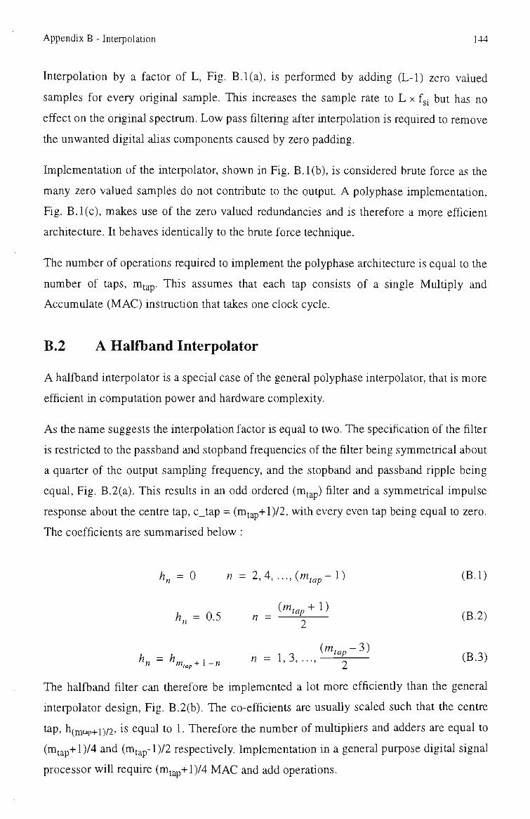
Appendix B - Interpolation 144
Interpolation by a factor of L, Fig. B.l (a), is performed by adding (L-1) zero valued
samples for every original sample. This increases the sample rate to L x f j but has no
effect on the original spectrum. Low pass filtering after interpolation is required to remove
the unwanted digital alias components caused by zero padding.
Implementation of the interpolator, shown in Fig. B.l(b), is considered brute force as the
many zero valued samples do not contribute to the output. A polyphase implementation.
Fig. B.l(c), makes use of the zero valued redundancies and is therefore a more efficient
architecture. It behaves identically to the brute force technique.
The number of operations required to implement the polyphase architecture is equal to the
number of taps, m ap. This assumes that each tap consists of a single Multiply and
Accumulate (MAC) instruction that takes one clock cycle.
B.2 A Halfband Interpolator
A halfband interpolator is a special case of the general polyphase interpolator, that is more
efficient in computation power and hardware complexity.
As the name suggests the interpolation factor is equal to two. The specification of the filter
is restricted to the passband and stopband frequencies of the filter being symmetrical about
a quarter of the output samphng frequency, and the stopband and passband ripple being
equal. Fig. B.2(a). This results in an odd ordered (mjap) filter and a symmetrical impulse
response about the centre tap, c_tap = (mtap+l)/2, with every even tap being equal to zero.
The coefficients are summarised below :
/j„ = 0 /7 = 2,4, . . . , ( m , , ^ - l ) (B.l)
(m,_„-i- 1) h^ = 0.5 n = —^ (B.2)
K = Kn,^,.i-n n = 1 , 3 , . . . , ^ ^ ^ ^ ^ (B.3)
The halfband filter can therefore be hnplemented a lot more efficientiy than the general
interpolator design. Fig. B.2(b). The co-efficients are usually scaled such that the centre
tap, fi(mtap+i)/2' is equal to 1. Therefore tiie number of multiphers and adders are equal to
(mjap+l)/4 and (mtap-l)/2 respectively. Implementation in a general purpose digital signal
processor witi require (mtap+l)/4 MAC and add operations.
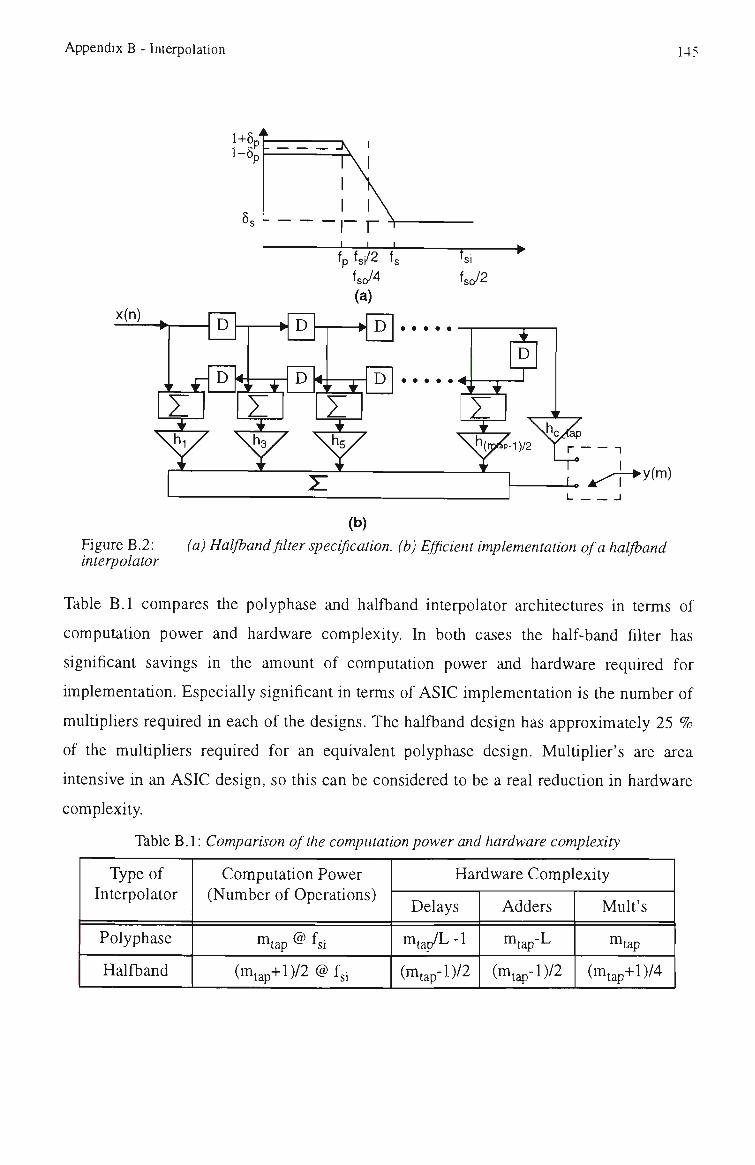
Appendix B - Interpolation 145
(b)
y(m)
I 1
Figure B.2: (a) Halfband filter specification, (b) Efficient implementation of a halfljand interpolator
Table B.l compares the polyphase and halfband interpolator architectures in terms of
computation power and hardware complexity. In botii cases the half-band filter has
significant savings in the amount of computation power and hardware required for
implementation. Especially significant in terms of ASIC implementation is the number of
multipliers required in each of the designs. The halfband design has approximately 25 %
of the multipliers required for an equivalent polyphase design. Multiplier's are area
intensive in an ASIC design, so this can be considered to be a real reduction in hardware
complexity.
Tkble B.l: Comparison of the computation power and hardware complexity
Type of Interpolator
Polyphase
Halfband
Computation Power (Number of Operations)
mtap @ fsi
(mtap+l)/2 @ f,i
Hardware Complexity
Delays
^tap/L -1
(mfap-l)/2
Adders
n tap-L
(mtap-l)/2
Muk's
n tap
(mtap+l)/4

Appendix C
DAC Survey
The following table has been comptied to survey the current state of the art in DAC
technology.
DAC's are hsted in order of their pubhshed precision (number of bits) and have been
included in the table on the basis of their stated maximum sampling frequency. The actual
sampling frequency at which they have been tested is also shown under <Max. fp'.
Commercially available DAC's seem to have a large discrepancy between the stated
maximum and tested maximum sampling frequency.
The Effective Number Of Bits (ENOB) refers to the effective precision of an operating
DAC. It is approxiamately related to the measured SFDR by the following formula.
SFDR (dB) = 6 X ENOB (C. 1)
Due to dynamic errors, the SFDR will reduce as the signal frequency increases. Thus
when a DAC is tested the SFDR is stated at a specified signal frequency, written as a
fraction of the samphng rate. Worse performance is guaranteed beyond the maximum
signal frequencies specified.
The glitch energy, rise and settiing time parameters are indicators of the dynamic
performance of DAC. Low values are required for good high speed performance.
146

Appendix C - DAC Survey 147
Precision
8
10
12
14
16
Published
Comm. Avail
Pubhshed
Comm. Avail
Pubhshed
Comm. Avail
Published
Comm. Avail
Published
Comm. Avail
Tabled Reference
[63]
Tri Quint
TQ6114
[61]
Harris
HI5721
[64]
Burr Brown DAC650
[60]
Tri Quint
SC-0806-C
[62]
Analog Devices AD768
: Current state of the art in DAC technology
Stated Max. fj
800MHz
1.5GHz
IGHz
125 MHz
IGHz
500MHz
>lGHz
IGHz
40MHz
30MHz
Measured Parameters
Max. fj.
800MHz
IGHz
IGHz
125MHz
IGHz
lOOMHz
750MHz
IGHz
lOMHz
lOMHz
SFDR (ENOB)
-
45dBc(7.5)@fs/17
58dBc(9.6)@ y iOO
53dBc(8.8)@ y 5
62.4(10.4)@ y i O
58dBc(9.6)@fs/4
50dBc(8.3)@ fJ2
60dBc(10)@ fJA
-43dBc(7.2)@ iJA
82dBc(13.4)@fs/8
83dBc(13.5)@yiO
Ghtch energy
3pV-s
lOpV-s
<lpV-s
1.5pV-s
4pV-s
20pV-s
<10pV-s
-
2.5pV-s
35pV-s
Rise
time^
380ps
300ps
500ps
-
180ps
500ps
300ps
350ps
2000ps
Setthng time*"
-
2ns
-
-
0.7ns
< 5ns
Ins
-
25ns
25ns
a. From 10->90% b. To settle within +/-0.5 LSB of final value.

Appendix D
The Carrier to Noise Ratio of a Quadrature Upconverter
The purpose of this appendix is to relate the carrier to noise ratio at the output of the
quadrature upconverter to the carrier to noise ratio at the output of each DAC.
For simplicity of calculations it has been assumed that a single channel is activated at RF.
The In Phase and Quadrature baseband signals, required to generate this RF signal, are
equivalent to a rotating phasor, given by:
Xi(t) = ajj cos( wt + e(t)) = y • (^ ^ " ^ e'^ ^ ") (D.l)
Xq(t) = ajjsin( wt + e(t)) = —. • (e'^ " -e '^ ^ ") (D.2)
For clarity, Eqns. (D.l) & (D.2) have been graphically represented as double sided spectra
m Fig. D.l. Each line has a power of magnitude (aj / 4). The In Phase and Quadrature
signals are then mixed with the quadrature phased carrier signals:
cosWct= --{e + e ) (D.3)
-smwct= - —-{e -e ) (D.4)
The resulting double sided line spectra can be mathematically described as:
^miW - j ( e +e +e +e ) (D.D)
148

Appendix D - The Carrier to Noise Ratio of a Quadrature Upconverter 149
Xmq(t) = "^k , ;((w^+«')f+e(r)) -j((w^+w)f + e(f)) 7((>v^.->v)r-8(r)) - ; ( ( K -M.);-e(;)i — (e -e + e -e ) (D.6)
The final stage combines these mixed signals to form the single channel at RF:
a I
s(t)= ^-{e jii^c + *v)' + 6(0) -7((w^ + vf )f + 9(0)
-I- e ) (D.7)
In this example, the carrier power measured at either the DAC or the output of the
quadrature upconverter are the same:
' carrier ~ % ' -^ (D.8)
The DAC quantisation noise is shown with a double sided power spectral density (PSD),
of magnitude No/2. This decreases to NQ/S after mixing with the quadrature phased carrier
signals. The In Phase and Quadrature noise power wtil then add at the combination stage,
resultmg in a PSD of NQM.
Xi(t)
, 4
^ ^ ' ^ o ^ ^ . ^ ^
BW
Xmi(t)
16
rf ^ -fc-f fc fc+f
/8
A 4
fc tcf '-'**meas - • ' s^-
lN^4
-f :f: -(fn-f)-f.-(fc+f) fc-f fc fc+f
k16
meas
Figure D.l: A quadrature upconverter, showing the line spectra (and corresponding power or power spectral density) at each stage in the process.

Appendix D - The Carrier to Noise Ratio of a Quadrature Upconverter 150
The noise power specified in a radio system is measured with a bandpass filter of
bandwidth of BWi gas- Therefore, the noise power measured at the output of the
quadrature upconverter is:
PN.QU = 2 X BWjneas x No / 4 = BW^as x No / 2 (D.9)
and at the output of the DAC:
PN-DAC = 2 X BW^eas x No / 2 = BW^eas > No (D. 10)
The carrier to noise ratio (CNR) at the output of the quadrature converter is therefore twice
that of the carrier to noise ratio at the output of each DAC. Although this example only
considers a single channel, the same will be true for a multi channel signal. Therefore, the
following relationship will hold:
CNRinuiti IRF = 2 X CNRjnuiti IDAC output (D-H)

Appendix E
The Schuchman 'Sufficiency Condition'
Schuchman [55] first developed a condition for the PDF of the dither signal to cause the
quantisation error to become a uniformly distributed white noise which is signal
independent. Reference [49] also showed that the Schuchman 'sufficiency condition'
implied that the sequence of quantisation errors was also independent. The Schuchman
condition only applies to ideal quantisers.
The Schuchman condition states that when the characteristic function of the dither signal
Xj, is equal to zero:
^,n j ^-—- 1 = 0 when 1 = all integers except 0 (E. 1)
then it is sufficient for the fotiowing properties to hold:
• The quantisation error, qe(X-i-Xj ), is independent of the input signal, X.
The quantisation error, qe(X-i-Xjj), is a uniformly distributed, [-A/2 A/2], random variable.
The characteristic function is defined as the Fourier transform of the PDF:
M^iju) = Eie'""^) (E.2)
= r p(W)e^''^dW J —oo
where p(W) refers to the PDF of the dither signal. The Schuchman 'sufficiency condition'
151

Appendix E - The Schuchman 'Sufficiency Condition' 152
assumes a stationary input process and an ideal quantiser is ideal which does not overload
(chp).
Apphcation of Equation (E.l) reveals some interesting properties of the three dither
probability density functions, uniform, Gaussian and triangular.
A Uniform PDF
Substitution of dither with a uniform PDF into (E.2) gives:
nyf / • \ f^"^ 1 }^^jTi sin(cw/2) , „ - , ^v^ju) = -e' dU = — , , (E.3)
J-C/2C cu/2 Applying the sufficiency condition, Eqn. (E.l), gives
Mu\ ; [ / - — = —-.—--—- = 0 when (/c/A) is all integers except 0 (E.4) V A y 7U/c/A
as lis defined as an integer [55] then it follows that
c = nA where n must be any integer except 0. (E.5)
Thus uniform dither with peak to peak amplitude excursions being multiples of the LSB
are part of the class of PDF's which satisfy Schuchman 'sufficiency condition'.
A Gaussian PDF
A Gaussian PDF is produced by the sum of N independent identically distributed
uniformly random variables:
N
G^ = X U. (E.6) J = 1
where G^ and Uj denote Gaussian and uniform PDF's respectively. The characteristic
function is therefore given by:
N
MGUU) = Yi^uiJu) (E.7) / = 1
where MQCJU) and MujCiu) denote Gaussian and uniform characteristic functions
respectively.
For the Gaussian PDF to meet the sufficiency condition all that is required is for one of the

Appendix E - The Schuchman 'Sufficiency Condition' 153
uniformly distributed functions to satisfy the condition specified in Eqn. (E.5). Further, it
has been shown [49] that if the standard deviation of the Gaussian PDF, CT, is greater than a
LSB, A, then MQ^U) (also referred to as the first order statistics) would be approximately
zero. Additionally, second order statistics show that the correlation between the input
signal and the quantisation error becomes negligible as CT/A, becomes large.
Thus Gaussian dither with a standard deviation greater than 1 LSB can be considered to
approximately satisfy the Schuchman 'sufficiency condition'. The approximation gets
better as the standard deviation is increased.
A Triangular PDF
Triangular dither is the sum of two uniformly distributed random variables with N set to 2
in Eqns. (E.6) & (E.7). For triangular dither to meet the 'sufficiency condition', the two
uniform distributions that make up the triangular distribution must satisfy the condition
specified in Eqn. (E.5). The triangular distribution is therefore bounded by:
t = nA where n is all integers except 0 (E.8)
the above examples have shown that uniform, Gaussian and triangular distributions are
part of a class of PDF's that satisfy the Schuchman 'sufficiency condition'. Given certain
restrictions, these PDF's force the quantisation error to be modelled as white noise.
However, the Schuchman condition only apphes to ideal quantisation functions, where the
quantisation levels are equally spaced.
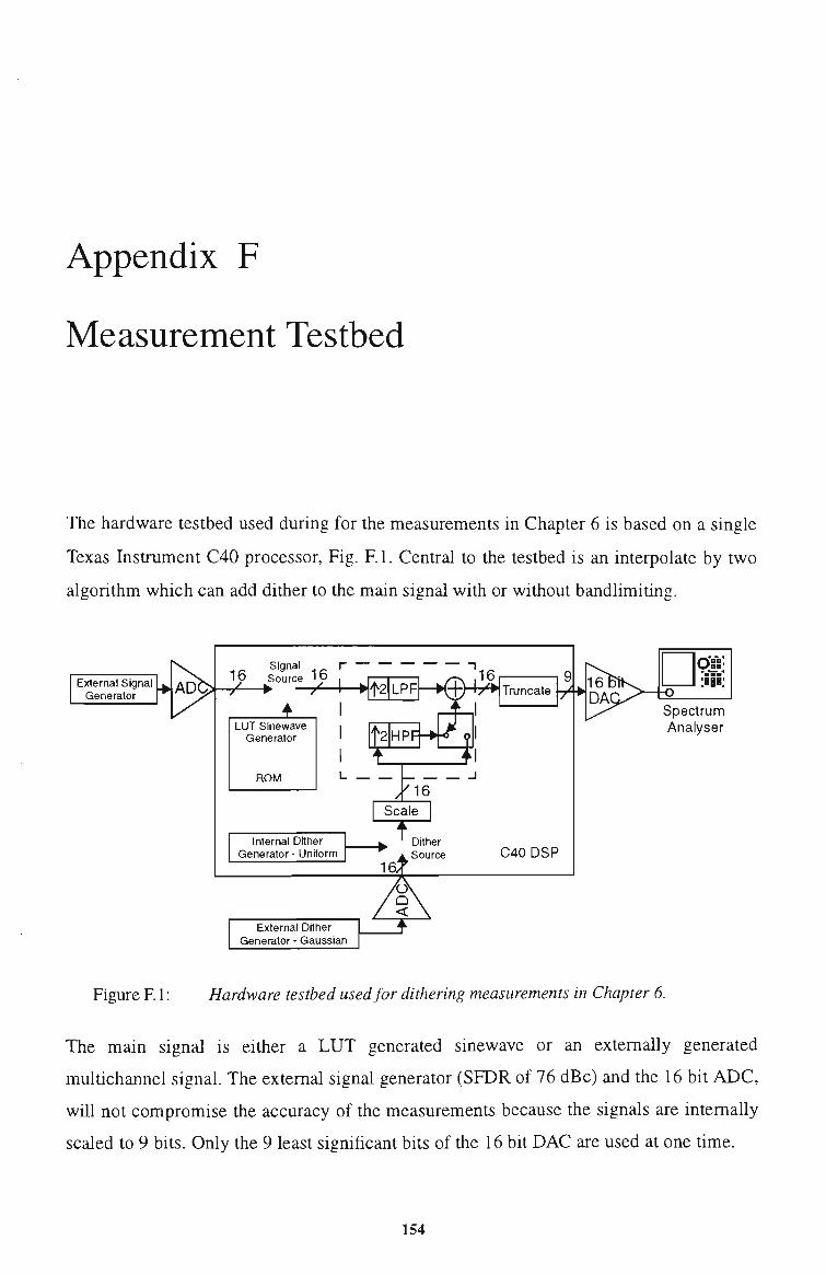
Appendix F
Measurement Testbed
The hardware testbed used during for the measurements in Chapter 6 is based on a single
Texas Instrument C40 processor. Fig. F. 1. Central to the testbed is an interpolate by two
algorithm which can add dither to the main signal with or without bandlimiting.
External Signal Generator
Signal Source I p
^ t2 |LPFh-K^
LUT Sinewave Generator
ROM
f2 HPf
I / 1 6
Scale
Internal Dither Generator - Uniform
16
I I
External Dither Generator - Gaussian
Tmncate
C40 DSP
16 •OlS
Spectrum Analyser
Figure F. 1: Hardware testbed used for dithering measurements in Chapter 6.
The main signal is either a LUT generated sinewave or an externally generated
multichannel signal. The external signal generator (SFDR of 76 dBc) and the 16 bti ADC,
wtil not compromise the accuracy of the measurements because the signals are intemaUy
scaled to 9 bits. Only the 9 least significant bits of the 16 bit DAC are used at one time.
154

Appendix F - Measurement Testbed 155
The bandlimited dither source can be selected from an internal generator, which is
wideband and uniformly distributed, or from an externally generated dither signal, which
is also wideband but Gaussian distributed. A Hewlett and Packard 3589A spectrum
analyser was used to perform the noise and spurious level measurements. During the
measurements the thermal noise floor of the spectrum analyser was at least 10 dB below
the quantisation noise floor of the DAC.

Bibliography
Chapter 2
[I] Reljonen, P., "GSM Base Station Development", Telecommunications, Vol 24, Edition 9, Sept. 1990, pp 85-92.
[2] Macario, R.C.V, "Personal and Mobile Radio Systems", Peter Peregrinus Ltd, London, UK, 1992, Chapter 12.
[3] Holbeche, R.J, "Land Mobile Radio Systems", Peter Peregrinus Ltd, UK, 1985, Chapter 4.
[4] Arnold, P.W & Seymour, K.J, "A New Frequency Agile Transmitter Combining System for North Americian Cellular", IEEE Vehicular Technology Society, 42"^ VTS Conference, 10-13 May, 1992, pp 1024-1033.
[5] Johnson, A.K & Myer, R, "Linear Amplifier Combiner", IEEE Vehicular Technology Conference, Tampa, Florida, 1987, pp 421-423.
[6a] Stefanov, J.J, "A Compact Base Station for Small Cells", Proceeding of the 3rd Nordic Seminar on Digital Land Mobile Radio Communications, Copenhagen, 1988, section 14-11.
[6b] Stefanov, J.J, "Designing Compact Base Stations for Urban Microcells", Digest of lEE Colloquium on "Microcellular Mobile Radio", London, 1989, pp 5/1-9.
[7] "Winning Team makes Waves", SERC Bulletin, UK, Vol. 5, No 1, Summer 1993, pp l2 .
[8] Manton, R.G, "Hybrid Networks and their uses in Radio Frequency Circuits", The Radio and Electronic Engineer, Vol. 54, Nov/Dec 1984, pp 473-489.
[9] European Telecommunications, pri-ETS 300 033-2, "Radio Transmission and Reception", Part 2, GSM Rec. 05.05, version 3.15.0.
[10] MPT 1317, Code of Practice, "Transmission of Digital Information over Land Mobile Radio Systems", Radiocommunications Agency, London, 1984, pp 8-9.
[II] MPT 1323, Performance Specification, "Angle Modulated Radio Equipment for use at Fixed and Mobile Stations in the Private Mobile Radio Service Operating in the Frequency Band 174-225 MHz", Radiocommunications Agency, London, reprint May 1993.
[12] "Superconducting Filter Screens Cellular Signals", Microwaves & RF, Dec 1994, pp 226.
[13] Hagstrom, U & Djuphamar, H, "RBS 884 - A New Generation Radio Stations for the American Standard", Ericsson Review, Sweden, No.l, 1994.
156

List of Principle Symbols and Abbreviations 157
[14] Kazeminejad, S., Howson, D.P. and Hamer, G., "Base Station multicoupler design for UK Cellular Radio Systems", Electonic Letters, Vol 23, No. 15. July 1987, pp 812.
[15] Zverev,A.I, "Handbook of Filter Synthesis", John Wiley and Sons, Inc. 1967.
[16] Kazeminejad, S., Howson, D.P., Baghai, A. and Hamer, G., "Cellular Radio Transmitter Combiners for Narrow Co-Channel Spacing", Fifth International Conference on Mobile Radio and Personal Communications, Coventry. UK, 11-14 December, 1989, pp 57-59.
[17] Kazeminejad, M., Khanifar A. & Howson, S.," Electronically Reconfigurable Cellular Radio Multicouplers", Fifth Intemational Conference on Mobile Radio and Personal Communications, Coventry, UK, 11-14 December, 1989, pp 103-106.
[18] Gans, M.J., "Some Properties of Multiple Carriers and Intermodulation", IEEE , pp 883-886.
[19] Radio Frequency Systems Product Catalogue (Australia).
[20] Stewart, R.D. & Tusubira, F.F., "Low Level Combining for Microcell Basestations", Digest of lEE Colloquium on "Microcellular Mobile Radio", London, 1989, pp 4/1-7.
Chapter 3
[21] Roome, S.J, "Analysis of Quadrature Detectors using Complex Envelope Notation", lEE proceedings. Vol 136, Part F, No. 2, April 1989, pp 95-100.
[22] Bridges, P., "Digital Demodulation Techniques for Radio channels". Masters Thesis, Victoria University of Technology, Australia, March 1993.
[23] Kaiser, J.F, "Nonrecursive Digital Filter Design using the I^-sinh Window Function", Proc. 1974 IEEE inter. Symp. on Circuits and Systems, April 1974.
[24] Bjerede, B., Lipowski, J., Petranovich, J. & Gilbert, S., 'An Intermediate Frequency Modulator using Direct Digital Synthesis Techniques for Japanese Personal Handy Phone (PHP) and Digital European Cordless Telecommunications (DECT)', IEEE Vehicular Technology Conference, Vol 1., Stockholm, Sweden, June 1994, pp 467-471.
[25] J.K.Caver, M.Liao, "Adaptive Compensation for Imbalance and Offset Losses in Direct Conversion Transceivers", IEEE Vehicular Technology Conference, St Louis, 1991, pp 578-583.
[26] M.Faulkner, T. Mattson, W.Yates, "Automatic Adjustment of Quadrature Modulators", Electronic Letters, Vol. 27, (3), Jan. 1991, pp 214-216.
[27] Scheuermann, H. & Gockler, H., "A Comprehensive Survey of Digital Transmultiplexing Methods", Proceedings of the IEEE, Vol. 69, No. 11, 1981, pp 1419-1450.

List of Principle Symbols and Abbreviations 15 8
[28] R.E.Crochiere & L.R.Rabiner, "Multirate Digital Signal Processing". Prentice Hall. 1983.
[29
[30
[31
[32
[33
[34:
[35
[36
[37
[38
[39
[40
[41
[42
[43
A. Bateman & W. Yates, "Digital Signal Processing", Pitman Publishing, 1988.
Buchanan, D., "Choose DACs for DDS System Applications", Microwaves and RF, August 1992, pp 89-98.
Blanchman, N.M, "Third-Order Intermodulation due to Quantisation". IEEE Trans, on Communications, Vol. COM-29, No. 9, Sept. 1991, pp 1386-1389.
Abuelma'atti, M.T, "The Intermodulation due to Multicarrier Quantisation", IEEE Transactions on Communications, Vol. COM-32, No. 11, Nov. 1984, pp 1211-1214.
Abuelma'atti, M.T, "Spectrum of a Nonlineariy Quantised Sinusoid", IEEE Proceedings, Vol. 136, Pt. G, No. 6, Dec. 1989, pp 313-316.
Abuelma'atti, M.T, "The Effect of Bit-Threshold Errors on the Harmonic and Intermodulation Performance of Successive Approxiamation A/D Converters", IEEE Transactions on Communications, Vol. COM-41, No. 8, Aug. 1993, pp 1155-1160.
Mitola, J, "The Software Radio Architecture", IEEE Communications Magazine, Vol. 33, No. 5, May 1995, pp 26-38.
Feher, K, "Filtering Inventions Enhance Digitally Modulated RF products". Microwaves & RF, April 1995, pp 140-148.
Papamichalis, P.E., "Digital Signal Processing with the TMS320 Family - Volume 3", Prentice Hall, Englewoods Cliffs, New Jersey, 1990.
Peled, A. & Bede, L., "A New Hardware Realization of Digital Filters", IEEE Transactions on ASSP, Vol. 22, No. 6, Dec. 1974, pp 456-462.
Hogenauer, E.B, "An Economical Class of Digital Filters for Decimation and Interpolation", IEEE Transactions on ASSP, Vol. 29, No. 2, April 1981, pp 155-162.
Goodman, D.J. & Carey, M.J., "Nine Digital Filters for Decimation and Interpolation", IEEE transactions on ASSP, Vol. 25, No. 2, April 1977, pp 121-126.
Coon, A., "Capabilities and Applications of SAW Coupled-Resonator Filters", Application Note AN-23, RF Monolithics, 4441 Sigma Road, Dallas, Texas, 1990.
Hill, A. & Surber, J., "Using Aliased-Imaging Techniques in DDS to Generate RF Signals", RF Design, Sept. 1993, pp 31-36.
Sinsky, A.I & Wang, P.C.P, "Error Analysis of a Quadrature Coherent Detector Processor", IEEE Transactions on Aerospace & Electronic Systems, Vol AES-10, Nov. 1974, pp 880-883.
List of Principle Symbols and Abbreviations ] 59
Chapter 4
[44] Churchiti, F.E.,Ogar, G.W. & Thompson, B.J., "The Cortection of I&Q ertors in a Coherent Processor", IEEE Transactions on Aerospace & Electronic Systems, Vol AES-17, No 1, Jan 1988, ppl31-136.
[45] Jones, A.E. & Gardiner, J.G, "Phase Error Correcting Vector Modulator for Personal Communications Network (PCN) Transceivers", Electronic letters. Vol 27, (14), July 1991, pp 1231-1232.
[46] Hilborn, D.,Stapleton, S.P. & Cavers, J.K., "An Adaptive Direct Conversion Transmitter", IEEE Transactions on Vehicular Technology, Vol. 43, No. 2, May 1994, pp 223-233.
[47] Sundstrom, L. & Faulkner, M., "The Effect of Reconstruction Filtering on the Predistortion Linearisation of RF Power Amplifiers", Mobile & Personal Communication Systems, Adelaide, Australia, 12-13 Nov., 1992, pp 357-361.
Chapter 5
[48] Blesser, B.A & Locanthi, B.N., "The Application of Narrow-Band Dither Operating at the Nyquist Frequency in Digital Systems to Provide Improved Signal-to-Noise Ratio over Conventional Dithering", Journal of Audio Engineering Society, Vol. 35, No 6, June 1987, pp 446-454.
[49] Sripad, A.B. and Snyder, D.L., "A Necessary and Sufficient Condition for Quantisation Errors to be Uniform and White", IEEE Transactions on Acoustics, Speech and Signal Processing, Vol. ASSP-25, Oct. 1977, pp 442-448.
[50] Vanderkooy, J. & Lipshitz, S.P., "Dither in Digital Audio", Journal Audio Engineering Society, Vol. 35, No 12, 1987 December, pp 966-975.
[51 ] Vanderkooy, J. & Lipshitz, S.P., "Digital Dither", presented at the 81 st Convention of the Audio Engineering Society, Journal of Engineering Society (abstracts). Vol. 34., December 1986, preprint 2412, pp 1030.
[52] Walpole, R.E. & Myers, R.H., "Probability and Statistics for Engineers and Scientists", Macmillan Publishing, 1985, Chapter 3.
[53] Jayant, N.S & Rabiner, L.R, "The Application of Dither to the Quantisation of Speech Signals", The Bell Sytem Technical Journal, Vol 51, No 6, July-Aug. 1972, pp 1293-1304.
[54] Bartz, M., "Large Scale Dithering Enhances ADC Dynamic Range", Microwaves and RF, May 1993, pp 192-198.
[55] Schuhman, L., "Dither signals and their Effect on Quantisation Noise", IRE Transactions in Communication Technology, Vol. COM-12, Dec. 1965, pp. 162-165.
[56] Bennet, W.R., "Spectra of Quantized Signal", Bell System Technical Journal, Vol. 27, July 1948, pp 446-472.

List of Principle Symbols and Abbreviations 160
[57] Papoulis, A., "Probability, Random Variables and Stochastic Processes". McGraw-Hiti Book Company, 1965.
Chapter 6
[58] 0'Rielly,J.J, "Series-Parallel Generation of m-sequences". Radio Electronic Engineering, Vol. 45, No 4, Aprti 1975, pp 171-176.
[59] Horowitz, P. & Hiti, W.,The Art of Electronics, Cambridge UK, Cambridge University Press, 1980.
Appendix C
[60] F.G.Weiss & T.G.Brown, "A 14 bit, 1 Gs/s DAC for Direct Digital Synthesis Applications", GAAs IC Symposium, pp 361-364.
[61] P. Vorenkamp, J. Verdaasdonk, R. Plassche & D. Scheffer, "A IGs/s, 10b Digital to analogue Converter", 1994 IEEE International Solid State Circuits Conference, pp 52-53.
[62] D. Mercer, "A 16-b D/A Converter with Increased Spurious Free Dynamic Range", IEEE Journal of Solid State Circuits, Vol. 29, No. 10., Oct. 1994, pp 1180-1185.
[63] K. Nojima & Y. Gendai, "An 8-b 800 MHz DAC", IEEE Journal of Solid State Circuits, Vol. 25, No. 6., Dec. 1990, pp 1353-1359.
[64] K-C. Hseih, T.A. Knotts, G.L.Baldwin & T. Homak, "A 12-bit 1-Gword/s GaAs Digital-to-Analog Converter System", IEEE Journal of Solid State Circuits, Vol. 22, No. 16., Dec. 1987, pp 1048 -1055.
Authors Published Papers
[65] Leyonhjelm, S.A., Faulkner, M. & Macleod, J., "The Effect of Reconstruction Filter Mismatch in a Digital Signal Processing Multichannel Combiner", IEEE International Conference on Universal Wireless Access, World Congress Centre, Melbourne, Australia, April 18-19, 1994, pp 25-30.
[66] Leyonhjelm, S.A. & Faulkner, M., "DSP Combining and Direct Conversion for Multichannel Transmitters", 43 lEEE/VTS Vehicular Technology Conference, Stockholm, Sweden,, Vol. 1 of 3, June 7-10, 1994, pp 494-498.
[67] Leyonhjelm, S.A. & Faulkner, M., "The Effect of Reconstruction Filters on Direct Upconversion in a Multichannel Environment", IEEE Transactions on Vehicular Technology, Vol. 44, No. 1, Feb. 1995, pp 95-102.
[68] Leyonhjelm, S.A., Faulkner, M. & Nilsson, P., "An Efficient Implementation of Bandlimited Dithering", Wireless Personal Communications, Accepted for publication on the 27*^ November, 1996.


The Effect of Reconstruction Filter IMismatch in a Digital Signal Processing JMultichannel Combiner
Scott A. Leyonhjelm, Student Member, IEEE, Michael Faulkner, Member, IEEE, and John Macleod. Member, IEEE.
Mobile Communications and Signal Processing Group,
Department of Electrical & Electronic Engineering,
Victoria University of Technology,
PO Box 14428 MMC, Melbourne, VIC 3000, AUSTRALIA.
Email: [email protected] [email protected]
Abstract - Traditionally multicarrier systems are combined in cumbersome and inflexible cavity filters. Future wireless systems will employ versatile and flexible combining techniques. This paper presents a DSP multichannel combiner incorporating a popular upconversion technique, direct conversion. The effect of mismatch in the reconstruction filters driving the direct conversion stage is analysed in a multichannel environment. It is shown that the reconstruction filters cause gain and phase imbalances to be frequency dependant, a significant issue when considering the stringent ACI requirements for radio communication systems. The paper also introduces an adaptive compensation technique as a means of overcoming these frequency dependant imbalances. Analysis reveals the sensitivity of direct upconversion in a multichannel environment to percentage mismatch and differing ACI level.
I. INTRODUCTION
Recent advances in the wideband linearisation of amplifiers suggest that Frequency Division Multiplex (FDM) systems can now be combined at low power levels [1-2]. The low power combination of channels can occur in a DSP environment, before being upconverted and amplified by a linear wideband amplifier, as illustrated below.
BWsy,/2 ' frequency
Sideband Rejection
frequency (b)
I-IllpiU
Q-lnpuL > • OUTPUT
Fig. 1. Analog Quadrature Modulation Llpconversion
This paper considers direct upconversion, using an analog quadrature modulator. This technique of upconversion has recently gained a lot of attention due to its suitability as a universal modulator (and demodulator); it is simple, small and has low power consumption. However a mismatch in the In phase and Quadrature (IQ) channels results in an undesired sideband, the magnitude of which is dependant upon the size of the gain and phase errors (imbalances) between the channels [3]. The imbalances are attributed to the non-ideal characteristics of the components, the mixers, summer, splitter and reconstruction filters. It is reasonable to talk of component imbalances (neglecting the reconstruction filters) of 0.3 dB and 3° in a well designed analog quadrature modulator.
Fig. 2. The effect of phase and gain imbalances in an analog quadrature modulator (a) Original signal displayed in complex baseband format, (b)
Desired and sideband (image) signals after passing through an unbalanced quadrature modulator.
Imbalances of this magnitude would result in 30 dB of sideband rejection, sufficient for some single channel applications.
The wideband upconversion application highlights a unique problem. A wideband FDM signal, Fig 2a, when passed through an unbalanced quadrature modulator, will result in both desired and sideband signals, Fig 2b. However different amounts of sideband rejection can be tolerated in a multichannel system. If the sideband signal falls into a channel that is being used then it will distort the desired signal (channel 1 in Fig. 2b), and the required sideband rejection is related to the E /No performance of the modulation. The sideband signal could equally fall into a vacant channel position (channel 7 in Fig. 2b). In this situation the system must meet the ACI specifications of the system which are normally specified between -50 dBc and -80 dBc, for Mobile Satellite and Private Mobile Radio (PMR) systems respectively.
The analog quadrature modulator is therefore not usable in a multichannel environment without some form of refinement. A number of correction techniques have subsequently evolved [5-8], all have concentrated on a single channel application. Implementation of one such correction technique, utilising the CRISIS network [8], corrected gain and phase imbalances to 0.02dB and 0.4° respectively. This is equivalent to 49 dB sideband rejection, a definite improvement, but unacceptable in most multichannel applications. Additionally the
IEEE International Conference on Universal Wireless Access, Melbourne, Australia, 18-19 April 1994

effectiveness of current compensation techniques decreases dramatically when the reconstruction filters are mismatched.
Previous analysis has generally neglected the significance of the effect of a mismatch in the reconstruction filters. It has been reported [9] that "in a predistortion linearising system the reconstruction filters are a major source of error ", but the analysis was restricted to a single channel (narrowband) system with predistortion.
The next section describes a novel compensation technique that is applicable to a multichannel environment. Whereas previous compensation techniques have only compensated for a single gain and phase imbalance, this novel method cancels at a number of frequencies across the system bandwidth.
Section III shows that the reconstruction filters are the major contributor to frequency dependant imbalances across a wide band and then examines the effect of frequency dependant imbalances on the sideband signal. It is shown that the error vector between the reconstruction filters in the IQ channels is related directly to the amount of sideband rejection.
Section IV uses the relationship found in section III to develop a methodology for analysing the performance of mismatched filters driving an analog quadrature modulator. Two parameters, oversampling ratio and 'channel to system bandwidth' ratio, are introduced to objectively judge the performance of the multichannel adaptive compensation technique.
Finally, analysis reveals the sensitivity of percentage mismatch and differing ACI specification in a multichannel environment.
II. A NOVEL METHOD FOR THE COMPENSATION OF GAIN AND PHASE IMBALANCES
The novelty of the technique revolves around the wideband low-level combiner, which is based on transmultiplexer technology. Transmultiplexers make use of the inherent redundancies of interpolation (N padded zeroes) and the uniform spacing of the channels to form an efficient multirate algorithm [10].
Figure 3 illustrates the proposed technique. N channels are combined through a transmultiplexer to form a wideband signal (as shown in Fig. 2a). The system bandwidth is then directly upconverted via an analog quadrature modulator. The inherent gain and phase imbalances will cause undesired sideband signals (as shown in Fig. 2b). The compensation method deliberately introduces a sideband component (through the complex coefficient C ,) which cancels the undesired sideband. The adaption technique measures the sideband power in a vacant channel using a tuned receiver ( error sensing circuitry in Fig. 3) and adjusts the complex coefficient (C,^) to minimise the power of the undesired signal.
The process described above is repeated for every channel in the system but only whilst the channel is vacant. The update rate is slow but this is not considered a problem as the gain and phase imbalances drift slowly with time.
\ « • r QRF
Error Sensing Circuitry
Fig. 3. Multichannel adaptive compensation technique for correcting gain and phase imbalances.
The compensation technique described has a number of advantages over previous adaptive correction techniques.
• Reduced Computational Load - The adaption algorithm and the scaling coefficient operate at the channel sampling rate, as opposed to the output sampling rate.
• Corrects for Frequency Dependant Imbalances across the System Bandwidth - Previous techniques only compensate for a single bulk gain and phase imbalance across the system band.
• Increased Sensitivity of Feedback Signal - This technique detects only the undesired signal, as opposed to both the desired and undesired signal [8], thus increasing the dynamic range of the correction network.
For an uncorrected analog quadrature modulator the power of the sideband will exceed ACI specifications (Fig. 4a). In practice it is necessary to reduce the power in the sideband to comply with a given ACI specification and so there is room for non-ideal cancellation. The multichannel compensation technique exploits this fact by cancelling the phase and gain imbalance at a single frequency (bulk imbalance) and the sideband will be completely removed at this frequency. However the frequency dependant imbalances mean that a differential phase and gain imbalance will remain across the remainder of the channel (differential imbalance), causing a residual sideband response (Fig. 4b).
BW,.
Phase Imbalance
Fig. 4. (a) Sideband response due to frequency dependant imbalances (b) Sideband response after cancellation of the channels bulk imbalance.
IEEE International Conference on Universal Wireless Access, Melbourne, Australia, 18-19 April 1994

To comply with an ACI specification the following condition must hold :
ACI = lOlog Powerin Sideband dBc (1) Powerin Signal
The ability to quantify the frequency dependant imbalances is important in analysing the performance of the multichannel adaptive compensation technique.
III. ANALYSIS O F FREQUENCY DEPENDANT IMBALANCES
A. Causes of frequency dependant imbalance in a direct upconverter
Frequency dependant gain and phase imbalances arise from both the quadrature modulator and the mismatch in the reconstruction filters.
The quadrature modulator consists of the mixer, splitter and summer components. The gain and phase through each of these components is dependant on frequency to some extent, although the amount of dependence will depend on the complex design strategies employed. This issue is beyond the scope of the paper.
A typical Mini Circuits IQ Modulator was chosen as an example (Table I generated from data sheet). It can be seen that over a channel bandwidth of 5 MHz around 54 dB of sideband rejection exists if the bulk imbalance is removed (leaving the differential imbalance). Whilst over 70 dB could be achieved if the bandwidth was reduced below 100 kHz.
Table I Absolute variation of gain and phase imbalance across a specified
bandwidth for a Mini Circuits IQ Modulator (MIQD 895)
Bandwidth Differential
gain Variation (dB)
Differential Phase Variation
(degree)
Residual Sideband
100 kHz
.iOO kHz
5 MHz
0.01
0.02
0.05
0.05
0.10
0.30
-70 dB
-64 dB
-54 dB
In most communication systems utilizing the FDM format the channel bandwidth is less than 200 kHz. Therefore to meet system ACI specifications the quadrature modulator would have to produce a slightly better performance than this example. Assuming that this is possible the quadrature modulator can be considered to have constant bulk imbalance across the channel band.
Frequency dependence is then apportioned entirely to the reconstruction filters, which will now be analysed.
B. The effect of filter mismatch on the sideband signal
To analyse the effects of filter mismatch, the reconstruction filters are modelled with relative gain mismatch, a ( / ) , and phase error from quadrature, 0^(/) (radians). The variable P(/) is used to account for the absolute attenuation characteristic (or gain transfer function) of the filter and serves to normalise the magnitude at any frequency. Fig. 5 summarises the model :
Fig. 5. Modelling the mismatch between reconstruction filters The amount of sideband rejection is given as the absolute
magnitude of the image vector divided by the absolute magnitude of the wanted signal (the form of which is same to the static case analysed in [3]) and is given by :
Sideband Rejection = [ — l'i(Ol
= 201og^i —^ (dB)
(2)
An alternative way of visualising the previous analysis is to consider the I and Q path filters as vectors. When they are matched they are both equal in magnitude and phase (Fig. 6a), subsequently causing no distortion or sideband response. When the filters are mismatched there exists a phase and gain difference (frequency dependence), this is illustrated in Fig. 6b.
error
P(/) P(/)
P(/)a(/)
P(/)
(a) (b) Fig. 6. (a) 1 and Q path filters matched (b) 1 and Q path filters mismatched
It can be shown that the error vector is related to the Sideband rejection by :
Sideband rejection = lerror_vectorl / 2*P(/) (3) This can be verified by calculating the magnitude of the
error vector in Fig. 6b for small gain and phase imbalances and comparing it to the approximate sideband rejection calculated in Eqn. (2).
For typical values of ACI specified by radio communication systems the sideband has to be of a magnitude that infers very small gain and phase mismatch. The magnitude of sideband rejection can therefore be accurately predicted from Eqn. (2).
A means of comparing the performance of the multichannel compensation technique is now introduced.
rv. METHODOLOGY FOR ANALYSING THE EFFECT OF
IEEE International Conference on Universal Wireless Access, IMelbourne, Australia, 18-19 April 1994
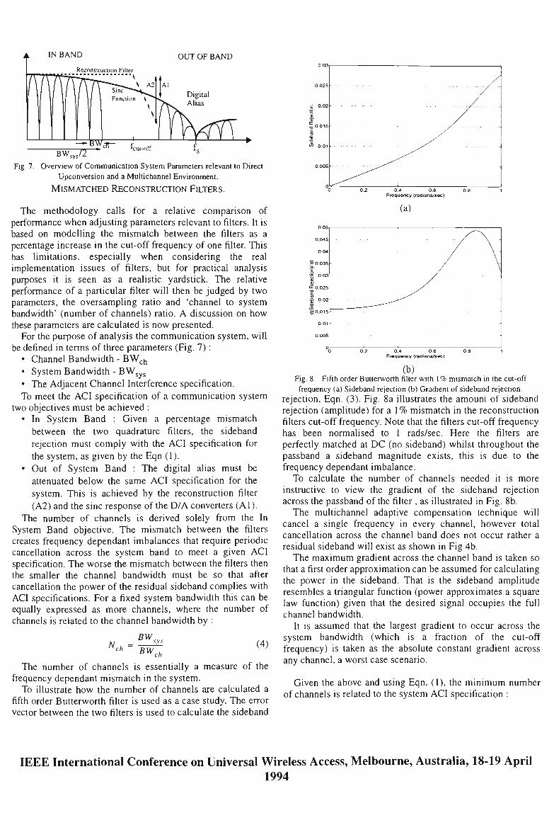
IN BAND
Reconsiruclion Filter
OUT OF BAND
Digital Alias
BW,y,/2
Fig. 7. Overview of Communication System Parameters relevant to Direct Upconversion and a Multichannel Environment.
MISMATCHED RECONSTRUCTION FILTERS.
The methodology calls for a relative comparison of performance when adjusting parameters relevant to filters. It is based on modelling the mismatch between the filters as a percentage increase in the cut-off frequency of one filter. This has limitations, especially when considering the real implementation issues of filters, but for practical analysis purposes it is seen as a realistic yardstick. The relative performance of a particular filter will then be judged by two parameters, the oversampling ratio and 'channel to system bandwidth' (number of channels) ratio. A discussion on how these parameters are calculated is now presented.
For the purpose of analysis the communication system, will be defined in terms of three parameters (Fig. 7):
• Channel Bandwidth - BW^h • System Bandwidth - BWjy^ • The Adjacent Channel Interference specification. To meet the ACI specification of a communication system
two objectives must be achieved : • In System Band : Given a percentage mismatch
between the two quadrature filters, the sideband rejection must comply with the ACI specification for the system, as given by the Eqn (1).
• Out of System Band : The digital alias must be attenuated below the same ACI specification for the system. This is achieved by the reconstruction filter (A2) and the sine response of the D/A converters (Al).
The number of channels is derived solely from the In System Band objective. The mismatch between the filters creates frequency dependant imbalances that require periodic cancellation across the system band to meet a given ACI specification. The worse the mismatch between the filters then the smaller the channel bandwidth must be so that after cancellation the power of the residual sideband complies with ACI specifications. For a fixed system bandwidth this can be equally expressed as more channels, where the number of channels is related to the channel bandwidth by :
Nci,= BW^
BW (4)
ch
The number of channels is essentially a measure of the frequency dependant mismatch in the system.
To illustrate how the number of channels are calculated a fifth order Butterworth filter is used as a case study. The error vector between the two filters is used to calculate the sideband
0.4 0.6 Frequency (radians/sec)
(a)
0.05
0.045
0.04
"S 0.035 •
I °° DC 0.025 •o c
•8 0.02
S^C.015
0.01
0.005
0 0.4 0.6
Frequency (radians/sec)
(b) Fig. 8. Fifth order Butterworth filter with 1 % mismatch in the cut-off frequency (a) Sideband rejection (b) Gradient of sideband rejection,
rejection, Eqn. (3). Fig. 8a illustrates the amount of sideband rejection (amplitude) for a 1% mismatch in the reconstruction filters cut-off frequency. Note that the filters cut-off frequency has been normalised to 1 rads/sec. Here the filters are perfectly matched at DC (no sideband) whilst throughout the passband a sideband magnitude exists, this is due to the frequency dependant imbalance.
To calculate the number of channels needed it is more instructive to view the gradient of the sideband rejection across the passband of the filter, as illustrated in Fig. 8b.
The multichannel adaptive compensation technique will cancel a single frequency in every channel, however total cancellation across the channel band does not occur rather a residual sideband will exist as shown in Fig 4b.
The maximum gradient across the channel band is taken so that a first order approximation can be assumed for calculating the power in the sideband. That is the sideband amplitude resembles a triangular function (power approximates a square law function) given that the desired signal occupies the full channel bandwidth.
It is assumed that the largest gradient to occur across the system bandwidth (which is a fraction of the cut-off frequency) is taken as the absolute constant gradient across any channel, a worst case scenario.
Given the above and using Eqn. (1), the minimum number of channels is related to the system ACI specification :
IEEE International Conference on Universal Wireless Access, Melbourne, Australia, 18-19 April 1994

300
BWsys normalised to fcut-off (a)
Oversampling ratio - fg / BWgys
(b) Fig. 9. Fifth order Butterworth filter with 1% mismatch in the cut-off
frequency complying with a 60 dB ACI specification (a) In System Band objective (b) Combination of In and Out Of System Band Objectives.
N BW,,,x
ch
^(sideband rejection)
df
10ACI/20xVl2 (5)
By varying the system bandwidth the minimum number of channels needed to comply with the systems ACI specification can be plotted as shown in Fig. 9a. As expected, more channels are needed as the system bandwidth approaches the cut-off frequency of the filter.
The second objective, Out of System Band, is achieved by attenuating the sampling aliases below the ACI specification. The filter attenuation characteristic will dominate the absolute sampling rate required to achieve this condition. The sampling frequency has been normalised to the Nyquist sampling rate of the system, BW^yj. This is expressed as the oversampling ratio :
Oversampling Ratio = / .v
BW. (6)
By combining the In and Out of System Band objectives the minimum number of channels can be related to the oversampling ratio for a given mismatch and system ACI specification, Fig. 9b. This methodology is now used to comparatively analyse the performance of the filters by modifying different parameters.
3 4 5
Oversampling ratio - f,
(a)
s/BWsys
3 4 5
Oversampling ratio - fj / BWsys (b)
Fig. 10. Fifth order Butterworth filter with a 1 % mismatch in the cut-off frequency and complies with a system specification of 60 dB ACI is assumed
unless otherwise stated (a) Percentage mismatch in the cut-off frequency varied (b) ACI specification varied.
V. NUMERICAL COMPUTATION AND ANALYSIS
The effect of mismatched reconstruction filters driving an analog quadrature modulator has been shown to introduce frequency dependant imbalances. These imbalances can be corrected by the adaptive compensation technique introduced in Section II. However the amount of mismatch in the reconstruction filters will put certain restrictions on the design, that is the number of channels and the oversampling ratio needed to comply with the systems ACI specification.
A. Filter Mismatch
Increasing the mismatch between the filters is the same as increasing the tolerance of the components used in implementing the filter This effect has been modelled as a percentage shift in the cut-off frequency.
For a small number of channels the oversampling ratio increases with an increase in percentage mismatch (Fig. 10a). However in a system with a large number of channels (140 and upwards) the amount of mismatch (as long as it is less than 5 %) becomes irrelevant as the oversampling limit (vertical asymptote in Fig. 10a) is reached.
The oversampling limit occurs when the system bandwidth
IEEE International Conference on Universal Wireless Access, Melbourne, Australia, 18-19 April 1994

equals the cutoff frequency, it is possible to go beyond this point by pre-emphasising the outer channels but this will not be considered here. The In System Band condition therefore determines the minimum number of channels, any further increase in the number of channels will improve the undesired sideband further below the ACI specification (In System Band condition) but will have no effect on the oversampling ratio. This is because the system bandwidth cannot be extended further and therefore the Out of System Band objective, which is not dependant on percentage mismatch, will govern the lowest oversampling ratio.
It can be concluded that the filters must be able to be designed to meet tight specifications and also be reliably reproduced in the manufacturing process.
B. ACI Specification
Increasing the ACI specification has a similar effect to increasing the percentage mismatch. Fig. 10b illustrates that the larger the ACI specification the higher the oversampling ratio required for a fixed number of channels. This is especially important for a small number of channels, say around 20, which for 70 dB ACI would require an oversampling ratio greater than 8. Depending on the bandwidth of the channel, such a large oversampling ratio will place severe limitations on the bandwidth of the system, primarily due to the sampling frequency that would be required for the digital processing.
Notice also that the oversampling limit decreases with a lowering of the systems ACI specification. To further lower this limit the filter order would have to be increased.
REFERENCES
[1] A.K.Johnson & R.Myer. "Linear amplifier combiner". IEEE VehicuUir Technology Conference, Tampa, Florida, pp 422-423.1987.
[2] J.Stefanov. "A compact base station for small cells"". Department of Electronics and Computer Science, Third Nordic Seminar on Digital Land Mobile Radio Communications, Copenhagen. 1988.
[3] A.I.Sinsky & P.C.P.'Wang, 'Terror Analysis of a quadrature coherent detector processor", IEEE Transactions on Aerospace and Electronic Systems, vol. AES-10, pp 880-883, Nov. 1974.
[4] S. Haykin, Digital Communications. John Wiley & Sons. Inc.. 1988. [5] F.E.Churchill,G.W.Ogar,B.J.Thompson. "The correction of l&Q errors
in a coherent processor", IEEE transactions on aerospace & electnmic systems. Vol AES-17, No 1, ppl31-136, Jan 1988.
[6] AJE.Jones and J.G.Gardiner, "Phase Error Correcting Vector Modulator for Personal Communications Network (PCN) Transceivers"', Electronic letters. Vol 27, (14), pp 1231-1232. July 1991.
[7] J.K.Cavers.M.Liao, "Adaptive compensation for imbalance and offset losses in direct conversion transceivers", IEEE transactions on Vehicular Technology, pp 581-588, 1991.
[8] M.Faulkner,TMattsson,W.Yates, "Automatic adjustment of quadrature modulators". Electronic letters. Vol 27, (3), pp 214-216, Jan. 1991.
[9] L.Sundstrom, M Faulkner. "The effect of reconstruction filtering on the predistortion linearisation of RF power amplifiers"'. Mobile & Personal Communication Systems, Adelaide, Australia, pp 357-361, 12-13 Nov 1992.
[10] R.E. Crochiere & L.R. Rabiner, Multirate Digital Signal Proce.<:sing. New Jersey : Prentice-Hall, Inc. 1983.
V. CONCLUSION
Mismatch between the reconstruction filters produce frequency dependant imbalances that cause undesired sideband responses in a multichannel environment. A novel adaptive compensation technique has been introduced to reduce these sideband signals to comply with radio communication system ACI specifications, nominally 50 to 80 dBc. The ability to correct for frequency dependant imbalances and the fact that the correction occurs at the channel sampling frequency are the two distinct advantages this technique possesses over previous adaptive compensation techniques.
Analysis of the frequency dependant imbalances yielded a relationship between the error vector of two mismatched filters and the amount of sideband rejection (ACI). This relationship was used to develop a methodology that related the number of channels to the oversampling ratio required to comply with a communication system ACI specification when the new adaptive compensation technique was employed.
The methodology objectively compared the performance of the system when mismatch in the reconstruction filters is considered. The main objective was to keep the oversampling ratio as low as possible, both for technology and power consumption reasons.
It was found that tightly matched reconstruction filter are required to minimise the oversampling ratio for a given ACI requirement.
IEEE International Conference on Universal Wireless Access, Melbourne, Australia, 18-19 April 1994


Digital Signal Processing and Direct Conversion for Multichannel Transmitters
Scott A. Leyonhjelm and Dr Michael Faulkner Mobile Communications and Signal Processing Group,
Department of Electrical & Electronic Engineering,
Victoria University of Technology,
PO Box 14428 MMC, Melbourne, VIC 3000, AUSTRALIA.
Email: [email protected] [email protected]
Abstract - A multichannel transmitter architecture is presented, combining an efficient transmultiplexer algorithm with direct conversion. Direct conversion is chosen for its simplicity and low cost, but it is necessary to compensate for the inherent amplitude and phase imbalances. These imbalances are shown to be frequency dependant in a multichannel environment, generating unacceptable levels of spurious sidebands and rendering current adaption techniques inappropriate. The paper proposes a compensation technique based on the multichannel transmitter architecture. It is computationally more efficient than the previous adaptive compensation techniques and simulations show that the undesired sideband can be controlled to meet ACI specifications.
I. INTRODUCTION
Recent advances in the wideband linearisation of amplifiers suggest that future Frequency Division Multiplex (FDM) systems can now be combined at low power levels. The low power combination can occur in a DSP environment, before being upconverted and amplified by a linear wideband amplifier.
A wideband low level combiner has numerous advantages over the conventional high power combining technique [1-2]. The flexibility of low level combining is further enhanced through the use of a DSP environment. The DSP algorithm performs the task of modulating and multiplexing the channels together into a FDM format. The broad class of algorithm that has been isolated for this specific task is called a transmultiplexer.
Extensive research during the 1970's (and early 1980's) revealed efficient transmultiplexer algorithms [3] that could interconnect two types of signals, Time Division Multiplex and Frequency Division Multiplex signals (SSB). More recently, satellite architectures [4] have incorporated these algorithms as a means to improve performance through increased flexibility, minimisation of weight and lower power consumption. Additionally these algorithms can be equally applied to the low-level power combining of digitally modulated signals.
Following the combination of channels, the band (centred at baseband) needs to be upconverted to radio frequency (RF). Direct conversion is one technique that has received a lot of attention due to its suitability as a universal
OUTPUT
Fig. 1. (a) Combined Digital Quadrature Modulation and Analog Heterodyne Upconversion. (b) Combined Analog Quadrature Modulation
and Heterodyne Upconversion. (c) Analog Quadrature Modulation Upconversion
modulator ( and demodulator); it is simple, small, has low power consumption, and can be applied to any modulation scheme. Unfortunately for a wideband system the specifications for Adjacent Channel Interference' are stringent, specifications range between -50 dBc to -80 dBc for Mobile Satellite and Land Mobile Radio (LMR) systems respectively. This paper will show that ACI is very sensitive to any mismatch in the I & Q paths, especially the reconstruction filters, of the direct converter.
Different versions of upconversion have been isolated for their suitability in a wideband application. They are illustrated in Fig. 1.
Digital quadrature modulation. Fig. 1(a), is limited by current DSP technology. The maximum sampling rate dictates the selection of the intermediate frequency (Ijp & Qjp), which ultimately limits the upconversion to a low intermediate frequency band. Consequently a double
1. Adjacent Channel Interference (ACI) "is a broad term. It includes next-channel (the channel next to the operating channel) interference and neighbouring-channel (more than one channel away from the operating frequency) interference" [5]. In the context of this paper it is used to infer any spurious signals produced by the combining and/or upconversion process
43' ' lEEEA^TS Vehicular Technology Conference, Stockholm, Sweden, June 7-10,1994.

conversion heterodyne approach is usually needed to complete the upconversion to the required RF band. The precision of a digital quadrature modulator overcomes the problems of gain and phase imbalance, DC offset and performance drift (all characteristics of the analog quadrature modulator) but there still exists some potential problems. These problems include :
• Replacing Analog with Digital processing increases the DC power consumption.
• Reduced spectral purity due to settling times and quantisation error of the DAC.
• The system in Fig. 1(a) requires approximately 3 dB more dynamic range than that of Fig. 1(b) and 1(c).
• The need for a heterodyne upconverter increases the cost and complexity.
The second method generates a higher intermediate frequency, allowing a simpler single upconversion heterodyne approach, as illustrated in Fig 1(b). The first bandpass filter reconstructs the signal and attenuates the digital aliases that are created by the D/A process. The intermediate frequency is chosen as a trade-off between the oversampling rate and bandpass filter rolloff. The gain and phase imbalances of the mixers and summer cause an undesired sideband signal that requires compensation if the system is to meet ACI specifications. The correction of these imbalances, assumed constant across the band of interest, has been previously addressed [6-9] and the novel technique presented in this paper is also applicable.
Analog quadrature modulation upconversion (Fig. 1(c)), or Direct Conversion, has recently gained a lot of attention through advances in RF device fabrication and also due to its suitability as a universal modulator. However, phase and gain imbalances force the need for compensation if it is to be used in modern day wideband wireless communication systems.
It can be shown that if a wideband channelised signal. Fig. 2(a), is passed through an unbalanced quadrature modulator, the result will consist of both wanted and sideband signals (Fig. 2(b)). The amount of sideband rejection is related to the amount of imbalance [10]:
Sideband Rejection = [Wanted Signal]
I Sideband Signal!
» 201og Ja 2 ^2 (1)
(dB)
B^\^/l frequencN
Sideband Rejection
Where a = Differential gain between the I & Q paths. 0 „ = Phase mismatch from an ideal of 1.57 radians.
frequency
Fig. 2. The effect of phase and gain imbalances in a quadrature modulator (a) Original signal displayed in complex baseband format, (b) Wanted and sideband (image) signals after passing through an unbalanced quadrature
modulator.
Different amounts of sideband rejection can be tolerated in a multichannel system. If the sideband signal falls into a channel that is being used then it will distort the desired signal (channel 1 in Fig. 2(b)). The required sideband rejection is then related to the E^/Nj, performance of the modulation scheme. The sideband signal could equally fall into a vacant channel posiUon (channel 7 in Fig. 2(b)). In this situation the system must meet the 50 dBc to 80 dBc system ACI specifications.
It is reasonable to talk of component imbalances (mixer and summer) of 0.3 dB and 3° in a well designed analog quadrature modulator. Imbalances of this magnitude would result in 30 dB of sideband rejection, sufficient for some single channel applications. The analog quadrature modulator is therefore not usable in a multichannel environment without some form of refinement. A number of correction techniques have evolved [6-9], all have concentrated on a single channel application. However the performance of these techniques is such that it is unacceptable in most multichannel applications. Furthermore the effectiveness of this type of compensation decreases dramatically when the reconstruction filters driving the analog quadrature modulator are mismatched.
The next section briefly reviews present compensation techniques and discusses their deficiencies. The novel method for the compensation of frequency dependant phase and gain imbalances in a multichannel environment is then introduced.
Section III proceeds to fully describe the novel method for compensation in a multichannel system. The technique utilises the most desirable features of the existing compensation techniques.
The adaption algorithm used in the simulations is briefly discussed in Section FV, whilst the simulations in Section V, verify the novel architecture, and also highlight the subtleties of its operation.
43*** lEEEA^TS Vehicular Technology Conference, Stockholm, Sweden, June 7-10,1994.

Adaption Algorithm
Error Sensing Circuitry
•4 A / D ^ - H -I
Fig. 3. Generic Adaptive Cancellation Architecture
II. TECHNIQUES FOR THE COMPENSATION OF GAIN AND PHASE IMBALANCES
Two recent methods of adaptive compensation have proved to be successful in narrow band applications. Although they have similar architectures (Fig. 3), there is a subtle difference to how the feedback (error) signal is obtained. The error signal is either detected from both the wanted and undesired signal [8] or in certain applications only the undesired signal is isolated [9].
The correction method, called CRISIS (CRoss-coupled Intra-Symbol Interference Suppression), that utilizes both the wanted and undesired signals [8], diode detects the RF power corresponding to a set of test vectors. The correction network coefficients are subsequently modified to minimise the measured error and therefore compensate for the quadrature modulator imbalance. This technique is limited in performance by :
• The wideband nature of the diode detector and the harmonic outputs of the mixer, which cause erroneous outputs. Pre-filtering improves but does not completely solve the problem.
• Drifting between measurements due to noise and 50 Hz pick-up.
• Quantisation error in the A/D limits the accuracy of the feedback signal.
Implementation of this technique corrected the gain and phase imbalances to 0.02 dB and 0.4° respectively. This is equivalent to 49 dB sideband rejection, barely meeting mobile satellite specifications. Theoretically the amount of compensation can be increased by detecting the unwanted signal alone, because without the larger wanted signal the dynamic range of the adaptive system is increased.
The correction network that utilizes this method (detecting only the unwanted signal) requires a non-linear amplifier to spread the spectrum. It filters out the wanted signal and uses the remaining adjacent channel interference to provide the necessary feedback information. The performance is still limited by the same problems experienced by the first technique, but to a lesser extent because the system is more sensitive to the error signal. The selectivity of the filter is critical to the ultimate performance of this correction technique.
Both systems suffer from the disadvantage that the actual
Fig. 4. Novel technique for compensation of gain and phase imbalances in a wideband multichannel system
compensation network requires additional processing at the output sampling frequency. The additional multiplications and additions are applied to each sample that is output. The high sampling rate required for the output of a wideband system makes the additional processing load of these adaptive corrective networks an unfavourable option.
The compensation systems discussed also imply that the gain and phase imbalances are constant across the system bandwidth. This may be valid when considering a single channel, but for many channels across the system bandwidth this assumption is not valid. Especially when the mismatch between the reconstruction filters is taken into account.
A novel method of compensation is now presented overcoming the two disadvantages mentioned above. That is, it reduces the computational load of and it can correct for variations in phase and gain imbalance across the system bandwidth.
III. A NOVEL METHOD FOR THE COMPENSATION OF PHASE AND GAIN IMBALANCES
The novelty of the technique revolves around combining the best features of techniques that have been discussed in previous sections. These techniques include a wideband low-level combiner, analog quadrature modulation upconversion and adaptive compensation of quadrature modulators.
A wideband low-level combiner is based on transmultiplexer technology [3], which makes use of the inherent redundancies of interpolation (N padded zeroes) and the uniform spacing of the channels to form an efficient multirate algorithm.
The quadrature modulator upconverter is chosen for its simplicity and low cost, although it is necessary to compensate for the imbalances so that ACI specifications are met.
The chosen adaption technique is based on a form of predistortion, that is the original signal is distorted in a predetermined manner such that the added distortion is cancelled by the following quadrature modulator network.
Figure 4 illustrates the proposed technique. Here N channels are combined through a transmultiplexer to form a
43' <* lEEEA^TS Vehicular Technology Conference, Stockholm, Sweden, June 7-10,1994.

wideband signal (as shown in Fig. 2(a)). The system band is then directly upconverted via an analog quadrature modulator. The inherent gain and phase imbalances will cause the sideband signals. The adaption technique then selects a vacant channel position and the undesired sideband (error) signal is isolated by the filter, increasing the dynamic range. This error signal is then sensed , by a diode detector, and used in the adaption algorithm to suitably modify the scahng coefficient (C^,) so that the feedback signal is minimised.
The process described above is repeated for every channel in the system but only whilst the channel is vacant. This infers slow adaption, and is not considered a problem as the gain and phase imbalances drift slowly with time.
Additionally as illustrated in Fig. 4, the scaling coefficient operates at the channel sampling rate, as opposed to the output sampling rate, thus substantially lowering the computational load on the system.
IV. ADAPTION ALGORITHM
The adaption algorithm is based on utilizing an error signal proportional to the magnitude of the sideband signal. The real and imaginary parts of the pre-distort coefficient are then adjusted accordingly using a simple one dimensional search technique [8].
The one dimensional search technique adjusts one part of the coefficient in incremental steps until the error begins to increase, the other coefficient is then selected for incremental adjustment. The process is repeated with reducing step sizes until the minimum is reached. Convergence is assured whilst the amount of sideband suppression achieved will depend on the final step size.
A faster algorithm could be implemented at the cost of more computational complexity.
V. SIMULATIONS
The compensation technique introduced in this paper and illustrated in Fig. 4 has been simulated to verify its operation.
Fig. 5(a) shows the output of an ideal quadrature modulator with three channels being activated by a single tone. Note that no sidebands are generated and adaption would not be necessary.
Introducing a bulk 10% gain and phase imbalance (constant across system bandwidth) into the quadrature modulator generates significant image signals, Fig 5(b). Obviously 20 dB sideband rejection is not a favourable result and will not achieve ACI specifications. Previous methods (see Section II) would actually be able to cancel this type of constant imbalance across the system bandwidth. But as Fig. 4 highlights, the compensation takes place at the higher sampling rate (CRISIS Network).
In a real wideband system gain and phase imbalances will vary across the system bandwidth, making them frequency dependant. Reasons for the variance include the frequency response of the mixers and summer and the mismatch in the reconstruction filters. This will result in
dB _ 0
-15 H
- 3 0
- 4 5
- 6 0 -
- 7 5 -f(Hz)
3e+0S 3 .5e+05 4e+05 4.5e-f05 5e-(-0.'> j g (a) No quadrature modulator imbalances
o""
-15 H
-30
-45 -
-60 -
-75 - f(Hz1
3e+05 3.5e-t-05 4e-(-05 4 . 5e+05 5e+05 (b) 10% phase and gain imbalance of a quadrature modulator only.
dB Q - l
- 1 5
- 3 0 - I
- 4 5
- 6 0
-75 H f(Hz) 3e-f05 3.5e-l-05 4e+05 4 . 5e-F05 5e+0!5
(c) 10% phase, gain and reconstruction hlter imbalance
- 1 5 -
- 3 0 -
- 4 5 -
- 6 0 -
- 7 5 -f(Hz)
3e-l-05 3 .50+05 4e+05 4 . 5e+05 5e+05 jp (d) CRISIS network compensation of imbalances in (c)
- 1 5 -
- 3 0 -
- 4 5 -
- 6 0 -
- 7 5 -1 f(Hz)
3e-^05 3 . 5e+05 4e+05 4.5e-l-05 5e+0!i (e) Multichannel adaptive compensation of imbalances in (c)
dB —I 0
- 1 5 -
- 3 0 -
- 4 5 -
- 6 0 -
- • ' S - I II I 11 I I [ II I K^Hz) 3e-l-05 3 .56+05 4e+05 4 . 5 e + 0 5 Se+OS
(0 Multichannel adaptive compensation of imbalances in (c)
Fig. 5. Simulation of the Novel Architecture presented in Fig. 4.
image signals that differ in level across the band. Fig. 5(c). The compensation networks based on the CRISIS
network can only cancel bulk gain and phase imbalance, and therefore if applied to a multichannel system only one of the image signals could be completely cancelled, as illustrated in Fig. 5(d). The other channels remain uncompensated.
43" ^ lEEEA^TS Vehicular Technology Conference, Stockholm, Sweden, June 7-10,1994.

BW, ch
Phase Imbalance
Residual jv A Sideband
(b) Single Compensation Point
Fig. 6. (a) Sideband response due to frequency dependant imbalances (b) Sideband response after cancellation of one channels bulk imbalance.
The new approach cancels all the image signals (Fig. 5(e)). Notice however that we are only representing the acfivation of a channel as a single tone at the centre of the channel, inferring that cancellation would also occur across the channel band. Unfortunately this is not the case, as Fig. 5(f) highlights. Here the channels are fully activated, and only one frequency in each image channel is completely cancelled. The rest of the channel still exhibits an unacceptable amount of sideband rejection.
Frequency dependence of these imbalances in wideband systems is far more cridcal than in single channel (narrowband) systems. This is because if the sideband falls into a vacant channel it must meet with ACI specifications of the system (50 to 80 dBc). To quantify the amount of mismatch that can be tolerated requires consideration of gain and phase variance across a single channel, not the whole system bandwidth. To explain this in more detail we need to consider the new adaptive technique together with the frequency dependant imbalances.
Fig. 6(a) illustrates how the magnitude of the sideband will vary across the channel bandwidth, a direct consequence of frequency dependant imbalances. The novel compensation technique can cancel out the phase and gain imbalance (bulk imbalance) at a single frequency, but not across the whole channel band. The differential phase and gain imbalance across the channel (differential imbalance) causes a residual sideband response that must be kept within ACI specifications (Fig. 6(b)). For every channel within the system bandwidth a similar scenario exists, therefore the technique cancels out a number of bulk imbalances across the system bandwidth.
VI CONCLUSION
A novel compensation technique has been presented in conjunction with a low power Digital Signal Processing based multichannel combiner.
The technique was shown to be less sensitive than that described in [8] to frequency dependant imbalances, which are significant in the wideband multichannel situation. The computational requirements are lower than previous adaption techniques, especially when not all the channels across the system are activated (normal situation).
The technique could equally be applied to the method of upconversion shown in Fig. lb, where a bandpass filter performs the reconstruction requirements. The major advantage is again in the lower computational requirements.
REFERENCES
[1] A.K.Johnson & R.Myer, "Linear amplifier combiner". IEEE Vehicular Technology Conference, Tampa. Flonda. pp 422-423. 1987.
[2] J.Stefanov, "A compact base station for small cells". Third Nordic Seminar on Digital Land Mobile Radio Communicati<ms. Copenhagen, 1988.
[3] H.Scheuermann, H.Gockler, "A comprehensive survey of digital transmultiplexing methods". Proceedings of the IEEE. Vol 69, No. l l ,pp 1419-1450, 1981.
4] A.D.Craig, C.K.Leong & A. Wishart, "Digital Signal Processing in Communications Satellite Payloads", Electrimics and Communication Engineering Journal, pp 107-114, June 1992,
[5] W.C.Y.Lee, Mobile Cellular Telecommunications Systems, McGraw Hill, pp 215, 1990.
[6] F.E.Churchill.G.W.Ogar.B.J.Thompson, "The correction of I&Q errors in a coherent processor", IEEE transactions on Aerospace & Electronic .nstems. Vol AES-17, No 1. ppl31-137, Jan 1988.
[7] J.K.Cavers & M.Liao, "Adaptive compensation for imbalance and offset losses in direct conversion transceivers", IEEE transactions on Vehicular Technology, pp 581-588, Nov. 1993.
[8] M.Faulkner.TMattsson.W.Yates, "Automatic adjustment of quadrature modulators". Electronic letters. Vol 27, (3), pp 214-216, 1991.
[9] D.Hilbom.S.P.Stapleton and J.K.Cavers, "An adaptive direct conversion transmitter", ^2'"' Vehicular Technology Conference, pp 764-767, May 1992.
[10] A.I.Sinsky & P.C.P Wang, "Error Analysis of a quadrature coherent detector processor", IEEE Tran.sactions on Aerospace & Electronic Systems, vol AES-17, No 1, pp 880-883, Nov. 1974.
An improvement to the single coefficient cancellation technique would be to replace it with an N tap equaliser (FIR filter) circuit. This would better match the phase and gain imbalances across the channel band at the expense of increased computaUonal complexity.
43' ' lEEEA^TS Vehicular Technology Conference, Stockholm, Sweden, June 7-10,1994.


The Effect of Reconstruction Filters on Direct Upconversion in a Multichannel Environment
Scott A. Leyonhjelm, Student Member, IEEE, and Michael Faulkner, Member, IEEE. Mobile Communications and Signal Processing Group,
Department of Electrical & Electronic Engineering,
Victoria University of Technology,
PO Box 14428 MMC, Melbourne, VIC 3000, AUSTRALIA.
Email: [email protected] [email protected]
Abstract - The effect of reconstruction filters on direct upconversion is analysed in a multichannel environment. It is shown that the reconstruction filters cause gain and phase imbalances to be frequency dependant, a significant issue when considering the stringent ACI requirements for radio communication systems. The paper introduces an adaptive compensation technique as a means of overcoming these frequency dependant imbalances Additionally the error vector between the mismatched filters is shown to be directly related to the amount of sideband rejection. This analysis is then used to develop a methodology for analysing the performance of the novel compensation technique with respect to the mismatched filters. Analysis of the classical all-pole filter algorithms reveal the sensitivity of direct upconversion in a multichannel environment to filter order, type, percentage mismatch and differing ACI level.
I. INTRODUCTION
Recent advances in the wideband linearisation of amplifiers suggest that Frequency Division Multiplex (FDM) systems can now be combined at low power levels [1-2]. The low power combination of channels can occur in a DSP environment, before being upconverted and amplified by a linear wideband amplifier, as illustrated below.
I-Inpm
Q-Inpiu > ^ OUTPUT
Fig. 1. Analog Quadrature Modulation Upconversion
This paper considers direct upconversion, using an analog quadrature modulator. This technique of upconversion has recently gained a lot of attention due to its suitability as a universal modulator (and demodulator); it is simple, small and has low power consumption. However a mismatch in the In phase and Quadrature (IQ) channels results in an undesired sideband, the magnitude of which is dependant upon the size of the gain and phase errors (imbalances) between the channels [3]. The imbalances are attributed to the non-ideal characteristics of the components, the mixers, summer, splitter and reconstruction filters. It is reasonable to talk of component imbalances (neglecting the reconstruction filters) of 0.3 dB and 3° in a well designed analog quadrature modulator.
Imbalances of diis magnitude would result in 30 dB of sideband rejection, sufficient for some single channel applications.
BW,y,/2 frequency
Sideband Rejection
frequency
Fig. 2. The effect of phase and gain imbalances in an analog quadrature modulator (a) Original signal displayed in complex baseband format, (b)
Desired and sideband (image) signals after passing through an unbalanced quadrature modulator.
The wideband upconversion application highlights a unique problem. A wideband FDM signal, Fig 2a, when passed through an unbalanced quadrature modulator, will result in both desired and sideband signals. Fig 2b. However different amounts of sideband rejection can be tolerated in a multichannel system.
If the sideband signal falls into a channel that is being used then it will distort the desired signal (channel 1 in Fig. 2b), as is the situation for a single channel quadrature modulator. The required sideband rejection is related to the Ei/N^ performance of the modulation. For example to achieve a bit error rate of 10" using the QPSK modulation technique the required Ei/Np is 7.5 dB [4] (Note : S/N - 2* EJH^ for QPSK). For the NADC system which uses QPSK, the distortion introduced by the imbalances would want to be 10 dB below this level so that there is no noticable effect. Additionally if power control is employed (35 dB from NADC specifications) then sideband rejection should be in the order of 50 to 60 dB so not to affect the error rate performance of the system.
The sideband signal could equally fall into a vacant channel position (channel 7 in Fig. 2b). In this situation the system
IEEE Transactions on Vehicular Technology, Vol. 44, No. 1, February 1995.

must meet the ACI specifications of the system which are normally specified between -50 dBc and -70 dBc, for Mobile Satellite and Private Mobile Radio (PMR) systems respectively.
The analog quadrature modulator is therefore not usable in a multichannel environment without some form of refinement. A number of correction techniques have subsequently evolved [5-9], all have concentrated on a single channel application. Implementation of one such correction technique, utilising the CRISIS network [8], corrected gain and phase imbalances to 0.02dB and 0.4° respectively. This is equivalent to 49 dB sideband rejection, a definite improvement, but unacceptable in most multichannel applications. Additionally the effectiveness of current compensation techniques decreases dramatically when the reconstruction filters are mismatched.
Previous analysis has generally neglected the significance of the effect of a mismatch in the reconstruction filters. It has been reported [10] that "in a predistortion linearising system the reconstruction filters are a major source of error ", but the analysis was restricted to a single channel (narrowband) system with predistortion.
The next section describes a novel compensation technique that is applicable to a multichannel environment. Whereas previous compensation techniques have only compensated for a single gain and phase imbalance, this novel method cancels at a number of frequencies across the system bandwidth.
Section III shows that the reconstruction filters are the major contributor to frequency dependant imbalances across a wide band and then mathematically analyses the effect of frequency dependant imbalances on the sideband signal. It is shown that the error vector between the reconstruction filters in the IQ channels is related directly to the amount of sideband rejection.
Section IV uses the relationship found in section III to develop a methodology for analysing the performance of mismatched filters driving an analog quadrature modulator. Two parameters, oversampling ratio and 'channel to system bandwidth' ratio, are introduced to objectively judge the performance of the multichannel adaptive compensation technique.
Analysis of the classical all-pole filter algorithms reveal the sensitivity of filter order, filter type, percentage mismatch and differing ACI specification in the novel compensation technique.
II. A NOVEL METHOD FOR THE COMPENSATION OF GAIN AND PHASE IMBALANCES
The novelty of the technique revolves around the wideband low-level combiner, which is based on transmultiplexer technology. Transmultiplexers make use of the inherent redundancies of interpolation (N padded zeroes) and the uniform spacing of the channels to form an efficient multirate algorithm [11].
Figure 3 illustrates the proposed technique. N channels are combined through a transmultiplexer to form a wideband signal (as shown in Fig. 2a). The system bandwidth is then directly upconverted via an analog quadrature modulator. The inherent gain and phase imbalances will cause undesired
sideband signals (as shown in Fig. 2b). The compensation method deliberately introduces a sideband component (through the complex coefficient C ,) which cancels die undesired sideband. The adaption technique measures the sideband power in a vacant channel using a tuned receiver ( error sensing circuitry in Fig. 3) and adjusts the complex coefficient (C^,) to minimise the power of the undesired signal.
The process described above is repeated for every channel in the system but only whilst the channel is vacant. The update rate is slow but this is not considered a problem as the gam and phase imbalances drift slowly with time.
' H- • ^
t^ ^
* Cm-I
1 , / ' -£4 v.»-^ i ^ I ' T ' ^ mf^^' m
Tra
nsm
ulti
plex
er
Alg
orit
hm
fii
N% ; (
• D/A
D/A ' F '
1 I
DSP
Adaption Algorithm
w#P%*V ' - -'
1
r 1
( A/D
( I
+•<% 4
Error Sensing Circuitry
Fig. 3. Multichannel adaptive compensation technique for correcting gain and phase imbalances.
The compensation technique described has a number of advantages over previous adaptive correction techniques.
• Reduced Computational Load - The adaption algorithm and the scaling coefficient operate at the channel sampling rate, as opposed to the output sampling rate.
• Corrects for Frequency Dependant Imbalances across the System Bandwidth - Previous techniques only compensate for a single bulk gain and phase imbalance across the system band.
• Increased Sensitivity of Feedback Signal - This technique detects only the undesired signal, as opposed to both the desired and undesired signal [8], thus increasing the dynamic range of the correction network.
For an uncorrected analog quadrature modulator the power of the sideband will exceed ACI specifications (Fig. 4a). In practice it is necessary to reduce the power in the sideband to comply with a given ACI specification and so there is room for non-ideal cancellation. The multichannel compensation technique exploits this fact by cancelling the phase and gain imbalance at a single frequency (bulk imbalance) and the sideband will be completely removed at this frequency. However the frequency dependant imbalances mean that a differential phase and gain imbalance will remain across the remainder of the channel (differential imbalance), causing a residual sideband response (Fig. 4b).
IEEE Transactions on Vehicular Technology, Vol. 44, No. 1, February 1995.

B W H
Residual KA Sideband
(b)
Fig. 4. (a) Sideband response due to frequency dependant imbalances (b) Sideband response after cancellation of the channels bulk imbalance.
To comply with an ACI specification the following condition must hold :
Ay^t ir.1 Powerin Sideband .^ ACI = lOlog-T^ :— — dB (1) Powerin Signal
The ability to quantify the frequency dependant imbalances is important in analysing the performance of the multichannel adaptive compensation technique.
III. ANALYSIS O F FREQUENCY DEPENDANT IMBALANCES
A. Causes of frequency dependant imbalance in a direct upconverter
Frequency dependant gain and phase imbalances arise from both the quadrature modulator and the mismatch in the reconstruction filters.
The quadrature modulator consists of the mixer, splitter and summer components. The gain and phase through each of these components is dependant on frequency to some extent, although the amount of dependence will depend on the complex design strategies employed. This issue is beyond the scope of the paper.
A typical Mini Circuits IQ Modulator was chosen as an example (Table I generated from data sheet). It can be seen that over a channel bandwidth of 5 MHz around 54 dB of sideband rejection exists if the bulk imbalance is removed (leaving the differential imbalance). Whilst over 70 dB could be achieved if the bandwidth was reduced below 100 kHz.
Table I
Absolute variation of gain and phase imbalance across a specified bandwidth for a Mini Circuits IQ Modulator (MIQD 895)
Differential Differential Bandwidth gain Variation Phase Variation
(dB) (degree)
Residual Sideband
100 kHz
-SOO kHz
5 MHz
0.01
0.02
0.05
0.05
0.10
0.30
-70 dB
-64 dB
-54 dB
In most communication systems utihzing the FDM format the channel bandwidth is less than 200 kHz. Therefore to meet ACI specifications of 70dB, the quadrature modulator would have to produce a slightly better performance than this example. Assuming that this is possible the quadrature modulator can be considered to have constant bulk imbalance across the channel band.
Frequency dependence is then apportioned entireh' to the reconstruction filters, which will now be analysed.
B. Mathematical Analysis - The effect of filter mismatch on the sideband signal
To analyse the effects of filter mismatch, the reconstruction filters are modelled with relative gain mismatch, a ( / ) , and phase error from quadrature, <t> (/) (radians). The variable P(/) is used to account for the absolute attenuation characteristic (or gain transfer function) of the filter and serves to normalise the magnitude at any frequency.
Let the gain of the I path be given by transfer function, p( / ) , of the ideal filter in question :
P(/) = P(/)(l + (a{/)/2)) - p ( / ) a ( / ) / 2 (2) and the gain of the Q path be given by a percentage change,
P(/) «(/) . in the transfer function of the ideal filter :
P(/)( l+«(/))= P(/)(l+(a(/)/2)) + p ( / ) a ( / ) / 2 (3) Similarly the phase mismatch between the filters is split
equally between the two paths, <I>^(/)/2. The quadrature modulator and DAC's are assumed to be ideal. These assumptions isolate the reconstruction filters as the source of error. Fig. 5 summarises the model :
Mnpui w
Q-Inpm ^
DSP
X X .
D/A
D/A
I
(t)
" O
P J-
J P(/)
^ J ( *
XQ(t)
- 7 ( *
>t> P(/)(l +«( / ) )
Fig. 5. Modelling the mismatch betvi'een reconstruction filters
The quadrature signal that is driven from the DSP, can be represented as a complex signal with a real (I channel) and an imaginary (Q channel) component. The same signal can be represented as a vector with an instantaneous magnitude and phase :
r(t) = x.{t) + jx^(l)
= \rit)\e^'"^ If there is no mismatch between the filters then the
(4)
IEEE Transactions on Vehicular Technology, Vol. 44, No. 1, February 1995.
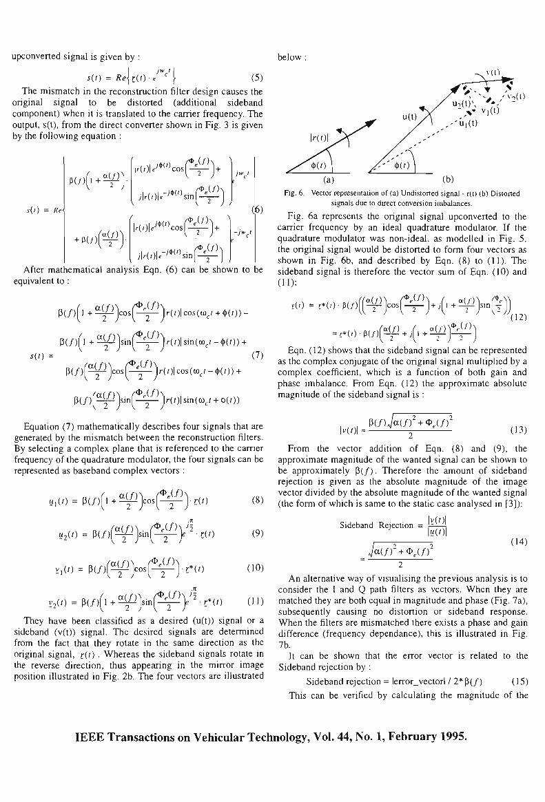
upconverted signal is given by :
sit) = Re\r(t)J''''\ (5)
The mismatch in the reconstruction filter design causes the original signal to be distorted (additional sideband component) when it is translated to the carrier frequency. The output, s(t), from the direct converter shown in Fig. 3 is given by the following equation :
v(r) = Re-
P(/) 1 + a(/)
+ P(/) «(/)
rOU-'^^^COS
M,)\e-J^^'hm
rCOU^f^^COsf-
,(/)- ^
r# .(/)
;iK')|. -mt) -r-4^1) -jw^i
(6)
After mathematical analysis Eqn. (6) can be shown to be equivalent to :
P(/) ( l + ^ ] c o s ( ^ ^ ) r ( / ) | cos(cD,r + 0(0) -
s{t) =
r(f)|sin(a)^r-(|)(r)) + (7)
P(/ ) (^]cos(^^^)r( / ) |cos(co, / - ( | ) (0) +
P ( / ) ( ^ ) s i n ( ^ ) r ( / ) | sin(a),r + ()>(?))
Equation (7) mathematically describes four signals that are generated by the mismatch between the reconstruction filters. By selecting a complex plane that is referenced to the carrier frequency of the quadrature modulator, the four signals can be represented as baseband complex vectors :
,.(0 = p(/)(i.£iLO)os(^).,(0
, (0 = p(,)(£lLO)in(^y r(t)
v,(0 = P(/) «( / ) |cos — ( / )
r*{t)
(8)
(9)
(10)
V2(0 = P ( / ) ( l + ^ ) s i n ( ^ ^ y ' r * ( 0 d D
They have been classified as a desired (u(t)) signal or a sideband (v(t)) signal. The desired signals are determined from the fact that they rotate in the same direction as the original signal, r{t). Whereas the sideband signals rotate in the reverse direction, thus appearing in the mirror image position illustrated in Fig. 2b. The four vectors are illustrated
below :
v(t)
/ -2(0
(a) (b)
Fig. 6. Vector representation of (a) Undistorted signal - r(t) (b) Distorted signals due to direct conversion imbalances.
Fig. 6a represents the original signal upconverted to the carrier frequency by an ideal quadrature modulator. If the quadrature modulator was non-ideal, as modelled in Fig. 5, the original signal would be distorted to form four vectors as shown in Fig. 6b, and described by Eqn. (8) to (11). The sideband signal is therefore the vector sum of Eqn. (10) and (11):
,(,) = ,*(,)• P ( 4 ^ > o s ( ^ ) . . ( , . « 4 > ) s . n f ^ - ) )
= !:*(/) •?(/) «(/) + j\i + «(/) ,* (/) (12)
Eqn. (12) shows that the sideband signal can be represented as the complex conjugate of the original signal multiplied by a complex coefficient, which is a function of both gain and phase imbalance. From Eqn. (12) the approximate absolute magnitude of the sideband signal is :
|v(0 P(/)Ja(/)^ + <I> (/)
(13) 2
From the vector addition of Eqn. (8) and (9), the approximate magnitude of the wanted signal can be shown to be approximately P(/) . Therefore the amount of sideband rejection is given as the absolute magnitude of the image vector divided by the absolute magnitude of the wanted signal (the form of which is same to the static case analysed in [3]):
Sideband Rejection = l^—[ l«(Ol
; « ( / ) ' +Oe(/) (14)
An alternative way of visualising the previous analysis is to consider the I and Q path filters as vectors. When they are matched they are both equal in magnitude and phase (Fig. 7a), subsequently causing no distortion or sideband response. When the filters are mismatched there exists a phase and gain difference (frequency dependance), this is illustrated in Fig. 7b.
It can be shown that the error vector is related to the Sideband rejection by :
Sideband rejection = lerror_vectorl / 2*P(/) (15)
This can be verified by calculating the magnitude of the
IEEE Transactions on Vehicular Technology, Vol. 44, No. 1, February 1995.
error
P(/) P(/)
P(/)cx(/)
(a) (b) Fig. 7. (a) I and Q path filters matched (b) I and Q path filters mismatched error vector in Fig. 7b for small gain and phase imbalances and comparing it to the approximate sideband rejection calculated in Eqn. (14).
For typical values of ACI specified by radio communication systems the sideband has to be of a magnitude that infers very small gain and phase mismatch. The magnitude of sideband rejection can therefore be accurately predicted from Eqn. (14).
A means of comparing the performance of the multichannel compensation technique is now introduced.
IV. METHODOLOGY FOR ANALYSING THE EFFECT OF MISMATCHED RECONSTRUCTION FILTERS.
The methodology calls for a relative comparison of performance when adjusting parameters relevant to filters. It is based on modelling the mismatch between the filters as a percentage increase in the cut-off frequency of one filter. This has limitations, especially when considering the real implementation issues of filters, but for practical analysis purposes it is seen as a realistic yardstick. The relative performance of a particular filter will then be judged by two parameters, the oversampling ratio and 'channel to system bandwidth' (number of channels) ratio. A discussion on how these parameters are calculated is now presented.
IN BAND
. .Reci)nstrucli.<)n_Filler, _ § i n i _ _ ' * Function
OUT OF BAND
Digital Alias
Fig. 8. Overview of Communication System Parameters relevant to Direct Upconversion and a Multichannel Environment.
For the purpose of analysis the communication system, will be defined in terms of three parameters :
• Channel Bandwidth - BW^^ • System Bandwidth - BW y • and the Adjacent Channel Interference specification -
ACI. To meet the ACI specification of a communication system
two objectives must be achieved : • In System Band : Given a percentage mismatch
between the two quadrature filters, the sideband rejection must comply with the ACI specification for the system, as given by the Eqn (1).
• Out of System Band : The digital alias must be attenuated below the same ACI specification for the system. This is achieved by the reconstruction filter (A2) and the sine response of the D/A converters (Al).
The number of channels is derived solely from the In System Band objective. The mismatch between the filters creates frequency dependant imbalances that require periodic cancellation across the system band to meet a given ACI specification. The worse the mismatch between the filters then the smaller the channel bandwidth must be so that after cancellation the power of the residual sideband complies with ACI specifications. For a fixed system bandwidth this can be equally expressed as more channels, where the number of channels is related to the channel bandwidth by :
!^ch = BW^ BW
(16) ch
The number of channels is essentially a measure of the frequency dependant mismatch in the system.
To illustrate how the number of channels are calculated a fifth order Butterworth filter is used as a case study. The error vector between the two filters is used to calculate the sideband rejection, Eqn. (15). Fig. 9a illustrates the amount of sideband rejection (amplitude) for a 1 % mismatch in the reconstruction filters cut-off frequency. Note that the filters cut-off frequency has been normalised to 1 rads/sec. Here the filters are perfectly matched at DC (no sideband) whilst throughout the passband a sideband magnitude exists, this is due to the frequency dependant imbalance.
To calculate the number of channels needed it is more instructive to view the gradient of the sideband rejection across the passband of the filter , as illustrated in Fig. 9b.
IEEE Transactions on Vehicular Technology, Vol. 44, No. 1, February 1995.

0.03
0.02S-
c 0.02
; 0.015-
" 0.01 •
0.006
0.4 0.6 Frequency (radians/sec)
(a)
0.4 0.6 Frequency (radians/sec)
(b) Fig. 9. Fifth order Butterworth filter with 1 % mismatch in the cut-off frequency (a) Sideband rejection (b) Gradient of sideband rejection.
The multichannel adaptive compensation technique will cancel a single frequency in every channel, however total cancellation across the channel band does not occur rather a residual sideband will exist as shown in Fig 4b.
If the gradient is assumed constant across the channel band then a first order approximation can be assumed for calculating the power in the sideband. That is the sideband amplitude resembles a triangular function (power approximates a square law function) given that the desired signal occupies the full channel bandwidth.
It is assumed that the largest gradient to occur across the system bandwidth (which is a fraction of the cut-off frequency) is taken as the absolute constant gradient across any channel, a worst case scenario.
Given the above and using Eqn. (1), the minimum number of channels is related to the system ACI specification :
^ch =
BW,„x '^(sideband rejection)
df
0.2 0.4 0.6 0.8
BWgys normalised to fpu, o« (a)
2 3 4 5 S 7 £) Oversampling ratio - fj / BWsyj
(b) Fig. 10. Fifth order Butterworth filter with 1% mismatch in the cut-off frequency complying with a 60 dB ACI specification (a) In System Band
objective (b) Combination of In and Out Of System Band Objectives. By varying the system bandwidth the minimum number of
channels needed to comply with the systems ACI specification can be plotted as shown in Fig. 10a. As expected, more channels are needed as the system bandwidth approaches the cut-off frequency of the filter.
The second objective. Out of System Band, is achieved by attenuating the sampling aliases below the ACI specification. The filter attenuation characteristic will dominate the absolute sampling rate required to achieve this condition. The sampling frequency has been normalised to the Nyquist sampling rate of the system, BWsys. This is expressed as the oversampling ratio :
Oversampling Ratio = /.. BW,
(18)
10ACi/20xVT2 (17)
By combining the In and Out of System Band objectives the minimum number of channels can be related to the oversampling ratio for a given mismatch and system ACI specification. Fig. 10b. This methodology is now used to
IEEE Transactions on Vehicular Technology, Vol. 44, No. 1, February 1995.

comparatively analyse the performance of the filters by modifying different parameters.
V. NUMERICAL COMPUTATION AND ANALYSIS
The effect of mismatched reconstruction filters driving an analog quadrature modulator has been shown to introduce frequency dependant imbalances. These imbalances can be corrected by the adaptive compensation technique introduced in Section II. However the amount of mismatch in the reconstruction filters will put certain restrictions on the design, that is the number of channels and the oversampling ratio needed to comply with the systems ACI specification.
By varying different parameters the methodology, which relates the number of channels in a communication system to the oversampling ratio, can be used to analyse the effect on performance.
Four parameters are considered :
A. Filter Mismatch
Increasing the mismatch between the filters is the same as increasing the tolerance of the components used in implementing the filter. This effect has been modelled as a percentage shift in the cut-off frequency.
For a small number of channels the oversampling ratio increases with an increase in percentage mismatch (Fig. 11a). However in a system with a large number of channels (140 and upwards) the amount of mismatch (as long as it is less than 5 %) becomes irrelevant as the oversampling limit (vertical assymptote in Fig. 11a) is reached.
The oversampling limit occurs when the system bandwidth equals the cutoff frequency, it is possible to go beyond this point by pre-emphasising the outer channels but this will not be considered here. The In System Band condition therefore determines the minimum number of channels, any further increase in the number of channels will improve the undesired sideband to further below the ACI specification (In System Band condition) but will have no effect on the oversampling ratio. This is because the system bandwidth cannot be extended further and therefore the Out of System Band objective, which is not dependant on percentage mismatch, will govern the lowest oversampling ratio.
It can be concluded that the filters must be able to be designed to meet tight specifications and also be reliably reproduced in the manufacturing process.
B. ACI Specification
Increasing the ACI specification has a similar effect to increasing the percentage mismatch. Fig. l ib illustrates that the larger the ACI specification the higher the oversampling ratio required for a fixed number of channels. This is especially important for a small number of channels, say around 20, which for 70 dB ACI would require an oversampling ratio greater than 8. Depending on the bandwidth of the channel, such a large oversampling ratio will place severe limitations on the bandwidth of the system, primarily due to the sampling frequency that would be required for the digital processing.
Notice also that the oversampling limit decreases with a lowering of the systems ACI specification. To further lower this limit the filter order would have to be increased.
C. Filter Type
The filters chosen contribute one desirable characteristic each; Maximum flat amplitude response, maximal flat group delay and the steepest roll-off obtained by the Butterworth. Bessel and Chebychev filters respectively. The cut-off frequency is defined as the frequency for which the filter attenuation has reached 3 dB.
The Chebychev filter is shown in Fig. l ie to have the best overall performance. The lowest oversampling limit is achieved by a higher ripple in the Chebychev filter, this is due to the inherently steeper roll-off. It is difficult to discern from Fig. l ie whether varying the ripple of the Chebychev filter increases performance below the oversampling limit. However as the ripple approaches zero the Chebychev response will approach the Butterworth response.
The Butterworth filter is comparable to the Chebychev filter, although it consistently has worse performance (albeit slightly).
The Bessel filter has difficulties achieving a low oversampling ratio, for a fifth order Bessel its oversampling limit is 2.8. This is mainly due to it's relatively slow roll-off and could be lowered by using a higher order filter.
D. Filter Order
Increasing the filter order lowers the oversampling limit because of the steeper roll-off. However for an increase in order there is not an equivalent improvement in performance, because a steeper roll-off is accompanied by a larger In System Band gradient. For example a system with 10 channels a fourth and sixth order filter requires an oversampling ratio of 6 and 5 respectively. Whereas increasing the order of the filter to ten has small gain in performance, the oversampling ratio is 4.7.
In a system that has many channels it would be better to use a higher order filter as long as the percentage mismatch could be guaranteed. The higher the filter order the more sensitive it is to component tolerances and its overall percentage mismatch will rise. However for a system with a small number of channels a lower order filter should be employed because of its reduced complexity and comparative performance to higher order filters.
IEEE Transactions on Vehicular Technology, Vol. 44, No. 1, February 1995.

300 300
3 4 5 Oversampling ratio -
(a)
fs/BWsys
300
3 4 5
Oversampling ratio -
(c)
fs/BWsys
Fig. 11. Fifth order Butterworth filter with a 1 % mismatch in the cut-off frequency and complies with a system specification of 60 dB ACI is assumed
unless otherwise stated (a) Percentage mismatch in the cut-off frequency varied (b) ACI specification varied, (c) Fifth order Chebychev (0.1 dB & 0.5 dB ripple), Bessel & Butterworth Filter types (d) Butterworth 4th, 6th & 10th
order filters
V. CONCLUSION
Mismatch between the reconstruction filters produce frequency dependant imbalances that cause undesired sideband responses in a multichannel environment. A novel adaptive compensation technique has been introduced to reduce these sideband signals to comply with radio communication system ACI specifications, nominally 50 to 70 dB. The ability to correct for frequency dependant imbalances and the fact that the correction occurs at the channel sampling frequency are the two distinct advantages this technique possesses over previous adaptive compensation techniques.
Analysis of the frequency dependant imbalances yielded a relationship between the error vector of two mismatched filters and the amount of sideband rejection (ACI). This relationship was used to develop a methodology that related
100
5 m tn 0} c c to sz o "o o 10 E z
::::::::: • ' • ' - .
I ! 1 1 r — 1 ••
\70dB ; ; ; ;
N^OdB ; ^ ^ ^ " " " " ^ - - - ^
\50dB ; ^-s^^^^
. 1 1 i — . I .
300
3 4 5 B
Oversampling ratio - fj / BW, (b)
sys
3 4 5 6 Oversampling ratio - fg / BWgys
the number of channels to the oversampling ratio required to comply with a communication system ACI specification when the new adaptive compensation technique was employed.
The methodology objectively compared the periformance of the system when four parameters were varied. The main objective was to keep the oversampling ratio as low as possible, both for technology and power consumption reasons.
It was found that the Chebychev filter offered the best overall performance no matter how many channels existed in the system. The order of the filter should be then chosen on the size of the system. For small systems (less than 10 channels) a low order filter offered lower complexity with comparable performance, however for larger systems a higher order filter offers increased performance. However for higher order filters an anomaly exists; due to their higher complexity they will be more sensitive to component tolerances, and therefore their ultimate performance will be degraded. Ultimately the achievable tolerance of the filter is the highest priority design issue.
IEEE Transactions on Vehicular Technology, Vol. 44, No. 1, February 1995.

REFERENCES
[1] A.K.Johnson & R.Myer, "Linear amphfier combiner", IEEE Vehicular Technology Conference, Tampa, Rorida, pp 422-423,1987.
[2] J.Stefanov, "A compact base station for small cells". Department of Electronics and Computer Science, The University of Southampton England.
[3] A.I.Sinsky & P.C.P.Wang, "Error Analysis of a quadrature coherent detector processor", IEEE Transactions on Aerospace and Electronic Systems, vol. AES-10, pp 880-883, Nov. 1974.
[4] S. Haykin, Digital Communications, John Wiley & Sons, Inc., 1988. [5] F.E.Churchill,G.W.Ogar,B .J.Thompson, "The correction of I&Q errors
in a coherent processor", IEEE transactions on aerospace & electronic systems. Vol AES-17, No 1, ppI31-136, Jan 1988.
[6] A.E.Jones and J.G.Gardiner, "Phase Error Correcting Vector Modulator for Personal Communications Network (PCN) Transceivers", Electronic letters. Vol 27, (14), pp 1231-1232, July 1991.
[7] J.K.Cavers,M.Liao, "Adaptive compensation for imbalance and offset losses in direct conversion transceivers", IEEE Vehicular Technology Conference, St Louis, pp 578-583, 1991.
[8] M.Faulkner.T.Mattson,W.Yates, "Automatic adjustment of quadrature modulators". Electronic letters. Vol 27, (3), pp 214-216, Jan. 1991.
[9] D.Hilbom,S.P.Stapleton and J.K.Cavers,"An adaptive direct conversion transmitter", IEEE Transactions on Vehicular Technology
[10] L.Sundstrom, M Faulkner, "The effect of reconstruction filtering on the predistortion linearisation of RF power amplifiers". Mobile & Personal Communication Systems, Adelaide, Australia, pp 357-361, 12-13 Nov. 1992.
[11] R.E. Crochiere & L.R. Rabiner, Multirate Digital Signal Processing, New Jersey : Prentice-Hall, Inc. 1983.
IEEE Transactions on Vehicular Technology, Vol. 44, No. 1, February 1995.

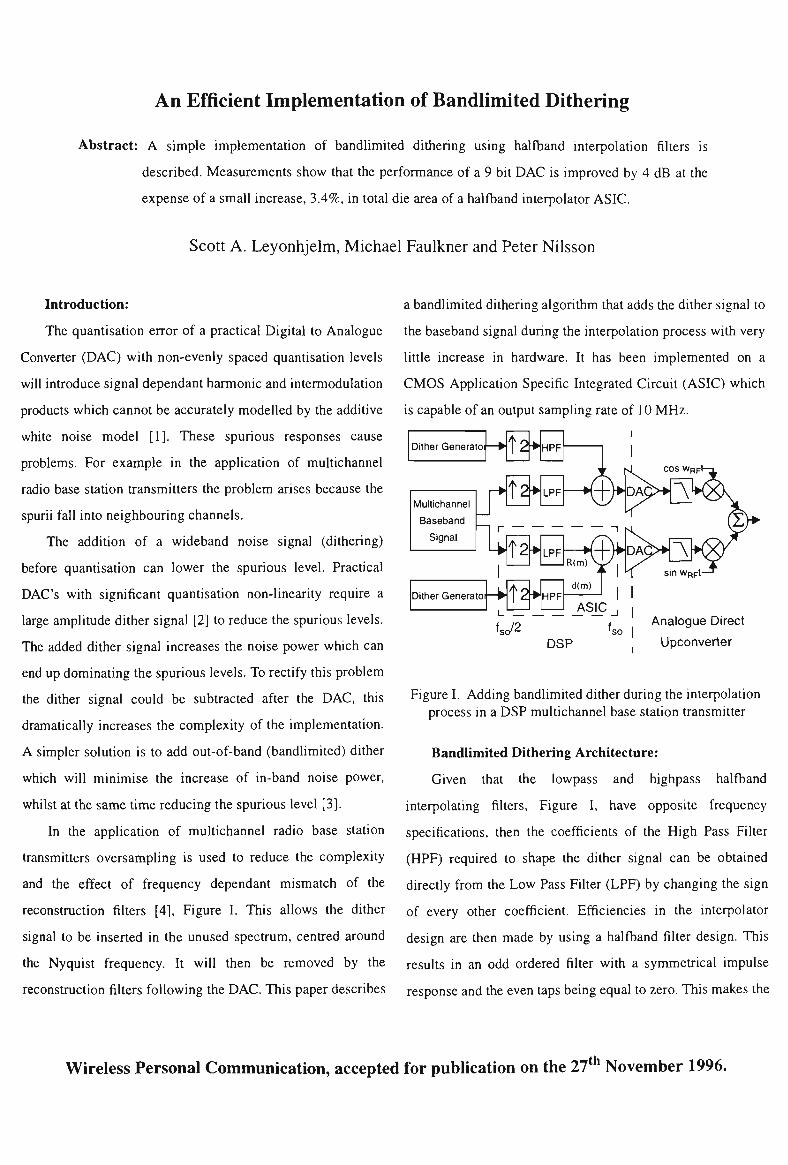
An Efficient Implementation of Bandlimited Dithering
Abstract: A simple implementation of bandlimited dithering using halfband interpolation filters is
described. Measurements show that the performance of a 9 bit DAC is improved by 4 dB at the
expense of a small increase, 3.4%, in total die area of a halfband interpolator ASIC.
Scott A. Leyonhjelm, Michael Faulkner and Peter Nilsson
Introduction:
The quantisation error of a practical Digital to Analogue
Converter (DAC) with non-evenly spaced quantisation levels
will introduce signal dependant harmonic and intermodulation
products which cannot be accurately modelled by the additive
white noise model [1]. These spurious responses cause
problems. For example in the application of multichannel
radio base station transmitters the problem arises because the
spurii fall into neighbouring channels.
The addition of a wideband noise signal (dithering)
before quantisation can lower the spurious level. Practical
DAC's with significant quantisation non-linearity require a
large amplitude dither signal [2] to reduce the spurious levels.
The added dither signal increases the noise power which can
end up dominating the spurious levels. To rectify this problem
the dither signal could be subtracted after the DAC, this
dramatically increases the complexity of the implementation.
A simpler solution is to add out-of-band (bandlimited) dither
which will minimise the increase of in-band noise power,
whilst at the same time reducing the spurious level [3].
In the application of multichannel radio base station
transmitters oversampling is used to reduce the complexity
and the effect of frequency dependant mismatch of the
reconstruction filters [4], Figure I. This allows the dither
signal to be inserted in the unused spectrum, centred around
the Nyquist frequency. It will then be removed by the
reconstruction filters following the DAC. This paper describes
a bandlimited dithering algorithm that adds the dither signal to
the baseband signal during the interpolation process with very
little increase in hardware. It has been implemented on a
CMOS Application Specific Integrated Circuit (ASIC) which
is capable of an output sampling rate of 10 MHz.
Dither Generatoi — • t2> HPF
Multichannel
Baseband
Signal
t2>LPF—•ff)>DA
I Dither Generatoi — •
tiUR—•ffiVDA I I iR(m) v y , /
t2> fso/2
HPF d(m)
ASIC
DSP
I I J I
Uo I Analogue Direct
Upconverter
Figure I. Adding bandlimited dither during the interpolation process in a DSP multichannel base station transmitter
Bandlimited Dithering Architecture:
Given that the lowpass and highpass halfband
interpolating filters. Figure I, have opposite frequency
specifications, then the coefficients of the High Pass Filter
(HPF) required to shape the dither signal can be obtained
directly from the Low Pass Filter (LPF) by changing the sign
of every other coefficient. Efficiencies in the interpolator
design are then made by using a halfband filter design. This
results in an odd ordered filter with a symmetrical impulse
response and the even taps being equal to zero. This makes the
Wireless Personal Communication, accepted for publication on the 27*** November 1996.

lowpass to highpass transformation trivial, with only the
centre tap requiring a change in sign. The two halfband
interpolating filters can now be easily merged to form a highly
efficient architecture as shown in Figure II.
R(n)
_r-i R(m)-i-d(m)
Switch toggled at a rate of fs„
Figure II. Halfband interpolator architecture with highpass dither shaping incorporated. Note that all components except for the switch operate at the input sampling rate, fso/2. R(n): Multichannel signal, d(n) : dither signal, L : adder, z" : sample delay, h^ : filter coefficient.
Compared to the lowpass interpolator, only two more
adders and a delay line (shown shaded in Figure II) are needed
to carry out the shaping and addition of dither. Thus the
benefits of bandlimited dithering using halfband interpolators
can be achieved for very little increase in circuitry. In the final
layout of the ASIC, the additional circuitry represented only
2.5% of the total die area. The wideband dither generator is
based on the Linear Feedback Shift Register Technique
(LFSR). The dither generator was designed using the
generation of m-sequences as a series of non-overlapping W
bit words [5]. The dither signal had only a positive magnitude
i.e. a DC offset of the half the dither amplitude. For the
generator to closely approximate white noise the m-sequence
length was set to 2'^^-l. Only 0.9% of the total die area was
used for this function.
Measurements:
The effect of the non-ideal 9 bit DAC is demonstrated in
Figure Ill(a), where four channels are activated. Only the
spurious responses that fall in-band or close to the edges of
the system bandwidth are considered in the calculation of the
Spurious Free Dynamic Range (SFDR), as the others will be
eliminated by the reconstruction filters. When no dither is
added the SFDR is 47 dBc and by adding bandlimited dither
the SFDR has increased to 53 dBc, Figure Ill(b). The out-of-
band dither has little effect on the in-band noise floor. The DC
offset of the dither Probability Density Function (PDF) has
also generated a sinusoid at t^J2, Figure Ill(b), and this
combined with the random dither signal can produce
additional benefits [6].
Ranga: -so dBm OvaraMaap: Ofr i S - O c t - i a a s 13:01 Has BH: 3 6 H i VBK: Off 3wc T lma: 7 7 . e z Sac B: SWEPT SPECTBUM Mkr 2 ISB H i - 3 a . 9 6 dBm
- 2 0 dBin
<p. - -
l O dB
/ d l v
*JUJ4
i k
SFDR = 47dBc
, ,
n JUi|Wi|WuiJjLi„, Li„
1 JklJiAi i l .yJ
f * " ^ "nwffwvfw
Centar; S5 OOO Hi
AVERAGING AVG: 10 Span: oo OOO Hz
(a)
Ranga: -20 dBm Ovarawaap: Off la-Oct-losg 13: as Raa BW: 36 Hz VBW: Off Swp Tlma: 77. aa Sac B: SWEPT SPECTRUM MIer S 13= Hi -3S . 08 dBm
- 2 0 dBm
LogMag
dB / d l v
^
- l a o 1 dBm i
Jiwv
iL
, _v ^ r J * ^
iBand !
^Fi:
? X. ^'
R - .c;.' HR<
y ^
r^
•\
' 1
sc /2
-TVITK
^^^m-Centar-: as OOO Hi
AVERAGING AVO: S
Span: SO OOO HI
(b) Figure III. (a) Four channels activated with no dither added.
fjp = 95kHz (b) Four channels activated with bandlimited dither added.
th
Wireless Personal Communication, accepted for publication on the 27 November 1996.

Figure IV shows that the SFDR only improves when there
is greater than lOOOA (where A is the average amplitude of
the Least Significant Bit in the measured 9 bit DAC) of dither
power. Note that when the dither level was increased, the
signal level was reduced so that the sum of the two signals did
not exceed the 9 bit full scale range of the DAC. In other
words, no clipping was allowed to occur.
65
60
u T! 55
50
45
CNR SFDR
SFDR with no dither added
10 10 10 10 Dither Power (LSB squared)
Figure IV. The effect of adding bandlimited dither.
The Carrier to Noise Ratio (CNR) is calculated using a
noise measurement bandwidth of BW^g^s. This bandwidth
can be obtained from radio system specifications e.g. 30 kHz
for GSM. As the bandlimited dither level increases, the in-
band noise floor remains approximately constant, but the
carrier power decreases, reducing the CNR. The SFDR and
CNR can now be combined into a quantity called the Carrier
to Noise and Distortion ratio (CaNAD), where the distortion
power is the sum of the noise and spurious power measured
within a bandwidth of BW^eas- The CaNAD for the worst
channel is defined as:
CaNAD = (SFDR" -i- CNR'^r^ (1)
For bandlimited dithering the SFDR dominates the CNR
for small values of dither power, whilst the reverse is true for
larger values of dither power. The CaNAD improves by 4 dB
when the SFDR and CNR are approximately equal. Observe
that small scale dither (amplitude variation in the order of 1
LSB) produces minimal improvement (<0.5dB), implying that
wideband dither would show no improvement unless the
dither can be subtracted after the DAC.
Conclusion:
Bandlimited dither has been added to the interpolated
baseband signal with a very small increase in hardware, 3.4%
of the total ASIC die area. The technique achieved a 4 dB
increase in performance for the 9 bit practical DAC measured.
Dither amplitude equal to half the full scale range of the DAC
was required to achieve this improvement.
Acknowledgements:
The Department of Applied Electronics, Lund University,
for providing the resources needed to design and fabricate the
ASIC's. The Australian Telecommunications and Electronic
Research Board and the DITAC Bilateral Science and
Technology Co-operation Program for providing financial
support.
Authors:
Scott A. Leyonhjelm received tiie B. S. degree from the University of Melbourne, Australia, in 1988, and in 1996 on the topic of wideband radio, he received the PhD degree froin the Victoria University of Technology, Australia. During 1989 he worked as an electrical engineer for Jannsen Phamiaceutica, Belgium, and Colstons Ltd., UK. During 1990 and 1991 he was employed at Philips Radio Communications Systems, Australia, engaging in Private Mobile Radio (PMR) products and research and development into a GMSK modem. After completing his PhD studies in 1995 he joined Ericsson Radio Systems, Sweden, as a design and development engineer. His current interests are in the area of wireless communication systems, including adaptive algorithms for feedforward linearisation and digital signal processing techniques for wideband radio.
Michael Faulkner received the B.Sc.(Eng) from Queen Mary College, London University, UK, in 1970, the M.E. degree from the University of New South Wales, Australia in 1978, and the PhD from University of Technology, Sydney in 1993. From 1975 to 1977 he was with the University of New South Wales, and since then as a lecturer and then Associate Professor at Victoria University of Technology, Melbourne, Australia. During 1983 he spent 6 months with Siemens Plessey working in military communications and between 1988 and 1996 he spent three periods at Lund University, Sweden, where he is currently visiting professor. His current interests are, signal processing, radio, circuit design and spread spectrum. Department of Electrical and Electronic Engineering, Victoria University of Technology, Melbourne, Australia.
Wireless Personal Communication, accepted for publication on the 27* November 1996.
Peter Nilsson was bom in Boriange, Sweden on December 9, 1958 and has grown up in SkSne in the south of Sweden. He received the M.S.E.E. at Lund University, Lund, Sweden m 1988. In February 1988 he joined the Department of Applied Electronics, Lund University, where he had made his diploma work and where he, in May 1992, received his Licentiate degree. In May 1996 he received the Ph.D. degree and is currently working as an Assistant Professor in the ASIC/DSP group at the same department. He's main interests are in the field of silicon implementation of custom DSP's related to the communication area, especially with parallel-serial architectures.
References:
[1] Bennet, W.R., "Spectra of quantized signal", Bell System
Technical Journal, Vol. 27, pp 446-472, July 1948.
[2] Bartz, M., "Large scale dithering enhances ADC
dynamic range", Microwaves and RF, pp 192-198, May
1993.
[3] Blesser, B & Locanthi, B., "The application of narrow
band dither operating at the Nyquist frequency in digital
systems to provide improved signal-to-noise ratio over
conventional dithering", J. Audio Eng. Soc, Vol. 35, No
6, pp 446-454, June 1987.
[4] Leyonhjelm, S. & Faulkner, M., "The effect of
reconstruction filters on direct upconversion in a
multichannel environment", IEEE Trans, on Veh. Tech.,
Vol. 44, No. 1, pp 95-102, Feb. 1995.
[5] O'Rielly, J.J.: 'Series-parallel generation of m-
sequences'. Radio Electronic Engineering, Vol. 45, No.
4, pp 171-175, 1975.
[6] Vanderkooy, J. & Lipshitz, S.P., "Dither in digital audio",
J. Audio Eng. Soc, Vol. 35, No 12, pp 966-975, Dec.
1987.
Wireless Personal Communication, accepted for publication on the 27* November 1996.