Embed Size (px)
Citation preview
VNWA Testboard kit for Ham Radio Workshop
This testboard kit was designed for the VNWA Workshop “Practical Use of Vector Network Analyzer” by Prof . Dr. Thomas Baier, DG8SAQ at Ham Radio Friedrichshafen on 29th and 30th June 2013. Tom's full presentation is available HERE : There is a separate Workshop Presentation showing only Workshop Experiments slides:
http://www.sdr-kits.net/DG8SAQ/VNWA/VNWA_Experiments.pdf
Basic Testboard Kit Contents:
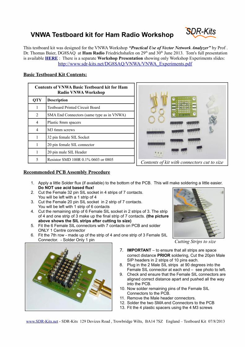
Contents of VNWA Basic Testboard kit for Ham Radio VNWA Workshop
QTY Description
1 Testboard Printed Circuit Board
2 SMA End Connectors (same type as in VNWA)
4 Plastic 8mm spacers
4 M3 6mm screws
1 32 pin female SIL Socket
1 20 pin female SIL connector
1 20 pin male SIL Header
5 Resistor SMD 100R 0.1% 0603 or 0805
Recommended PCB Assembly Procedure
1. Apply a little Solder flux (if available) to the bottom of the PCB. This will make soldering a little easier. Do NOT use acid based flux!
2. Cut the Female 32 pin SIL socket in 4 strips of 7 contacts. You will be left with a 1 strip of 4
3. Cut the Female 20 pin SIL socket in 2 strip of 7 contacts. You will be left with 1 strip of 6 contacts
4. Cut the remaining strip of 6 Female SIL socket in 2 strips of 3. The strip of 4 and one strip of 3 make up the final strip of 7 contacts. (the picture above shows the SIL strips after cutting to size)
5. Fit the 6 Female SIL connectors with 7 contacts on PCB and solder ONLY 1 Centre connector
6. Fit the 7th row - made up of the strip of 4 and one strip of 3 Female SIL Connector. - Solder Only 1 pin
7. IMPORTANT – to ensure that all strips are space correct distance PRIOR soldering, Cut the 20pin Male SIP headers in 2 strips of 10 pins each.
8. Plug in the 2 Male SIL strips at 90 degrees into the Female SIL connector at each end – see photo to left.
9. Check and ensure that the Female SIL connectors are aligned correct distance apart and pushed all the way into the PCB.
10. Now solder remaining pins of the Female SIL Connectors to the PCB.
11. Remove the Male header connectors. 12. Solder the two SMA end Connectors to the PCB13. Fit the 4 plastic spacers using the 4 M3 screws
www.SDR-Kits.net - SDR-Kits 129 Devizes Road , Trowbridge Wilts, BA14 7SZ England – Testboard Kit 07/8/2013
Cutting Strips to size
Contents of kit with connectors cut to size
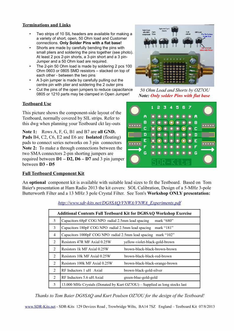
Terminations and Links
• Two strips of 10 SIL headers are available for making a a variety of short, open, 50 Ohm load and Customer connections. Only Solder Pins with a flat base!
• Shorts are made by carefully bending the pins with small pliers and soldering the pins together (see photo). At least 2 pcs 2-pin shorts, a 3-pin short and a 3 pin-Jumper and a 50 Ohm load are required.
• The 2-pin 50 Ohm load is made by soldering 2 pcs 100 Ohm 0603 or 0805 SMD resistors – stacked on top of each other - between the two pins
• A 3-pin jumper is made by carefully pulling out the centre pin with plier and soldering the 2 outer pins
• Cut the pins of the open jumpers to reduce capacitance 0805 or 1210 parts may be clamped in Open Jumper!
Testboard Use
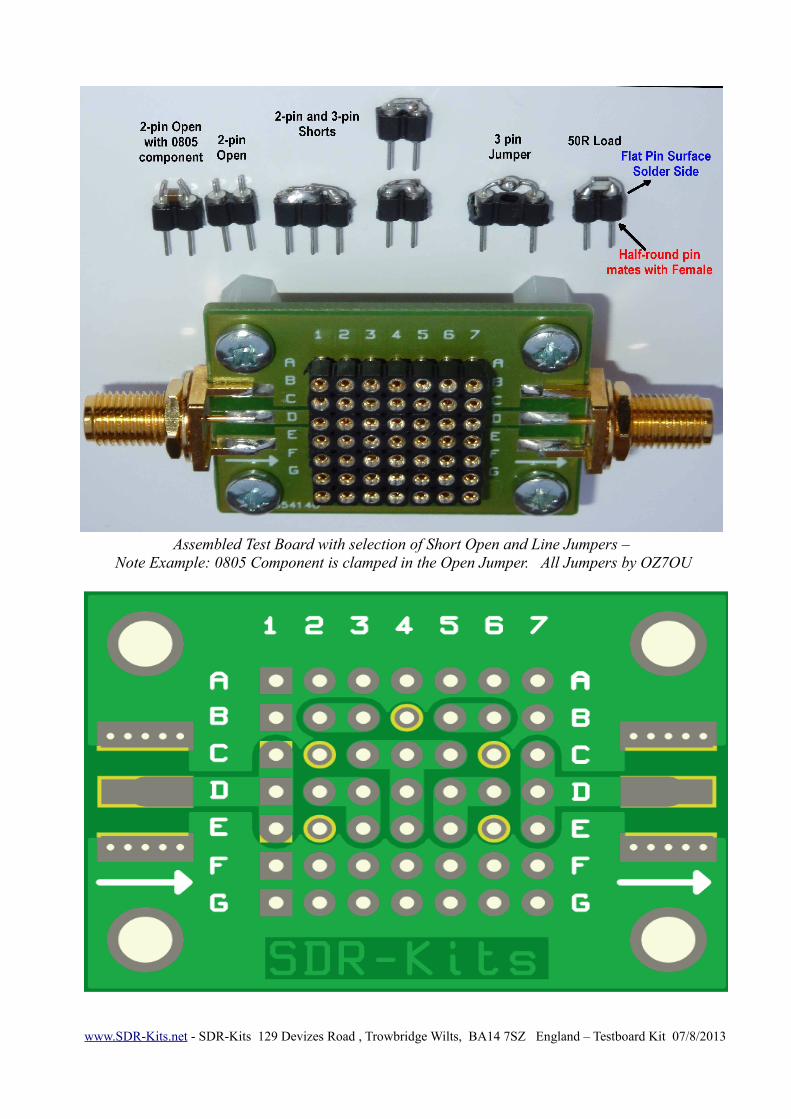
This picture shows the component-side layout of the Testboard, normally covered by SIL strips. Refer to this dwg when planning your Testboard ckt lay-outs
Note 1: Rows A, F, G, B1 and B7 are all GND. Pads B4, C2, C6, E2 and E6 are Isolated (floating) pads to connect series networks on 3 pin connectorsNote 2: To make a through connections between the two SMA connectors 2-pin shorting jumpers are required between D1 – D2, D6 – D7 and 3 pin jumper between D3 - D5
Full Testboard Component Kit
An optional component kit is available with suitable lead sizes to fit the Testboard. Based on Tom Baier's presentation at Ham Radio 2013 the kit covers: SOL Calibration, Design of a 5-MHz 3-pole Butterworth Filter and a 13 MHz 3 pole Crystal Filter. See Tom's Workshop ONLY presentation:
http://www.sdr-kits.net/DG8SAQ/VNWA/VNWA_Experiments.pdf
Additional Contents Full Testboard Kit for DG8SAQ Workshop Exercise
5 Capacitors 68pF COG NPO radial 2.5mm lead spacing mark “680”
3 Capacitors 180pF COG NPO radial 2.5mm lead spacing mark “181”
4 Capacitors 1000pF COG NPO radial 2.5mm lead spacing mark “102”
2 Resistors 47R MF Axial 0.25W yellow-violet-black-gold-brown
2 Resistors 1k MF Axial 0.25W brown-black-black-brown-brown
2 Resistors 10k MF Axial 0.25W brown-black-black-red-brown
2 Resistors 100k MF Axial 0.25W brown-black-black-orange-brown
2 RF Inductors 1 uH Axial brown-black-gold-silver
2 RF Inductors 5.6 uH Axial green-blue-gold-gold
5 13.000 MHz Crystals (Donated by Kurt OZ7OU) – Supplied as long stocks last
Thanks to Tom Baier DG8SAQ and Kurt Poulsen OZ7OU for the design of the Testboard!
www.SDR-Kits.net - SDR-Kits 129 Devizes Road , Trowbridge Wilts, BA14 7SZ England – Testboard Kit 07/8/2013
50 Ohm Load and Shorts by OZ7OU Note: Only solder Pins with flat base
www.SDR-Kits.net - SDR-Kits 129 Devizes Road , Trowbridge Wilts, BA14 7SZ England – Testboard Kit 07/8/2013
Assembled Test Board with selection of Short Open and Line Jumpers – Note Example: 0805 Component is clamped in the Open Jumper. All Jumpers by OZ7OU