Embed Size (px)
Citation preview
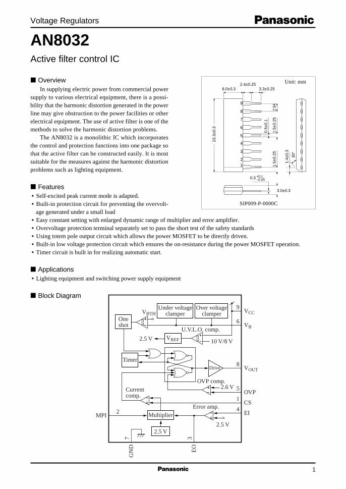
Voltage Regulators
1
AN8032Active filter control IC
OverviewIn supplying electric power from commercial power
supply to various electrical equipment, there is a possi-bility that the harmonic distortion generated in the powerline may give obstruction to the power facilities or otherelectrical equipment. The use of active filter is one of themethods to solve the harmonic distortion problems.
The AN8032 is a monolithic IC which incorporatesthe control and protection functions into one package sothat the active filter can be constructed easily. It is mostsuitable for the measures against the harmonic distortionproblems such as lighting equipment.
Features• Self-excited peak current mode is adapted.• Built-in protection circuit for preventing the overvolt-
age generated under a small load• Easy constant setting with enlarged dynamic range of multiplier and error amplifier.• Overvoltage protection terminal separately set to pass the short test of the safety standards• Using totem pole output circuit which allows the power MOSFET to be directly driven.• Built-in low voltage protection circuit which ensures the on-resistance during the power MOSFET operation.• Timer circuit is built in for realizing automatic start.
Applications• Lighting equipment and switching power supply equipment
Block Diagram
SIP009-P-0000C
9
8
7
6
5
4
3
21
0.3 +0.1–0.05
23.3
±0.3
6.0±0.32.4±0.25
3.3±0.25
1.5±
0.25
0.5±
0.1
2.54
1.5±
0.25
1.4±
0.3
3.0±0.3
30°
Unit: mm
VCCUnder voltage
clamper9
VB
VBTH
VREF 10 V/8 V
2.5 V
2.5 V
2.6 VCurrentcomp.
Error amp.
OVP comp.
U.V.L.O. comp.6
CS1
EI4
MPI2
EO
3
GN
D7
Over voltageclamper
Oneshot
TimerDrive
Multiplier
2.5 V
OVP5
VOUT8
2
AN8032 Voltage Regulators
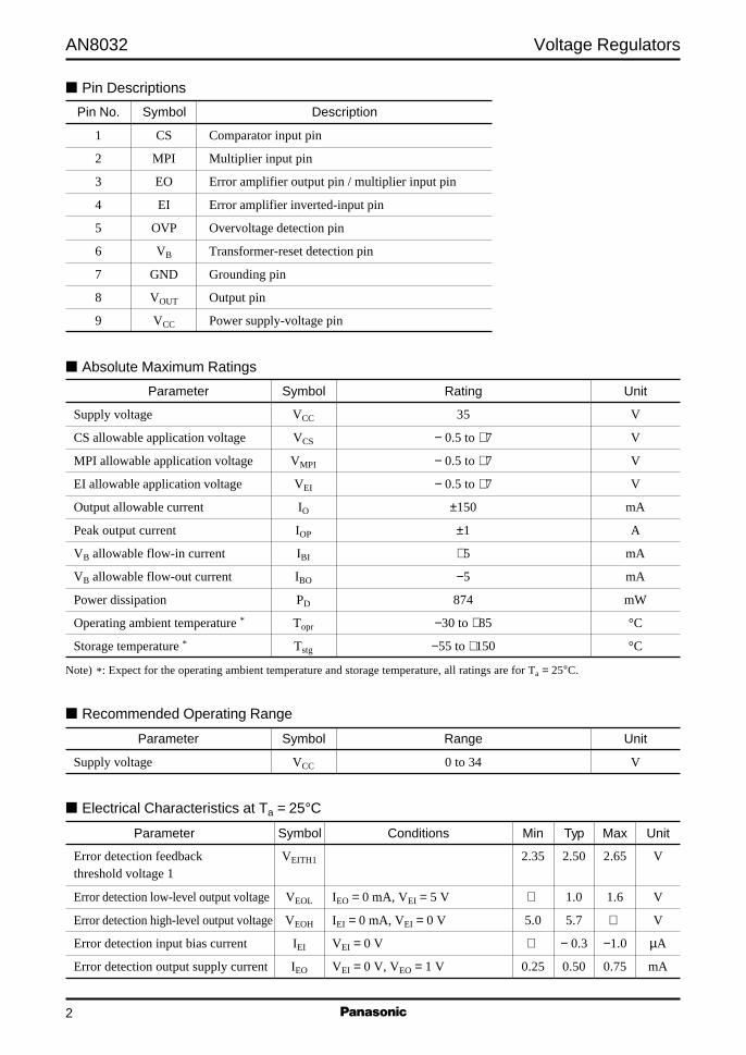
Parameter Symbol Range Unit
Supply voltage VCC 0 to 34 V
Absolute Maximum Ratings
Parameter Symbol Rating Unit
Supply voltage VCC 35 V
CS allowable application voltage VCS − 0.5 to +7 V
MPI allowable application voltage VMPI − 0.5 to +7 V
EI allowable application voltage VEI − 0.5 to +7 V
Output allowable current IO ±150 mA
Peak output current IOP ±1 A
VB allowable flow-in current IBI +5 mA
VB allowable flow-out current IBO −5 mA
Power dissipation PD 874 mW
Operating ambient temperature * Topr −30 to +85 °C
Storage temperature * Tstg −55 to +150 °C
Recommended Operating Range
Electrical Characteristics at Ta = 25°C
Parameter Symbol Conditions Min Typ Max Unit
Error detection feedback VEITH1 2.35 2.50 2.65 Vthreshold voltage 1
Error detection low-level output voltageVEOL IEO = 0 mA, VEI = 5 V 1.0 1.6 V
Error detection high-level output voltageVEOH IEI = 0 mA, VEI = 0 V 5.0 5.7 V
Error detection input bias current IEI VEI = 0 V − 0.3 −1.0 µA
Error detection output supply current IEO VEI = 0 V, VEO = 1 V 0.25 0.50 0.75 mA
Pin Descriptions
Pin No. Symbol Description
1 CS Comparator input pin
2 MPI Multiplier input pin
3 EO Error amplifier output pin / multiplier input pin
4 EI Error amplifier inverted-input pin
5 OVP Overvoltage detection pin
6 VB Transformer-reset detection pin
7 GND Grounding pin
8 VOUT Output pin
9 VCC Power supply-voltage pin
Note) * : Expect for the operating ambient temperature and storage temperature, all ratings are for Ta = 25°C.
3
Voltage Regulators AN8032
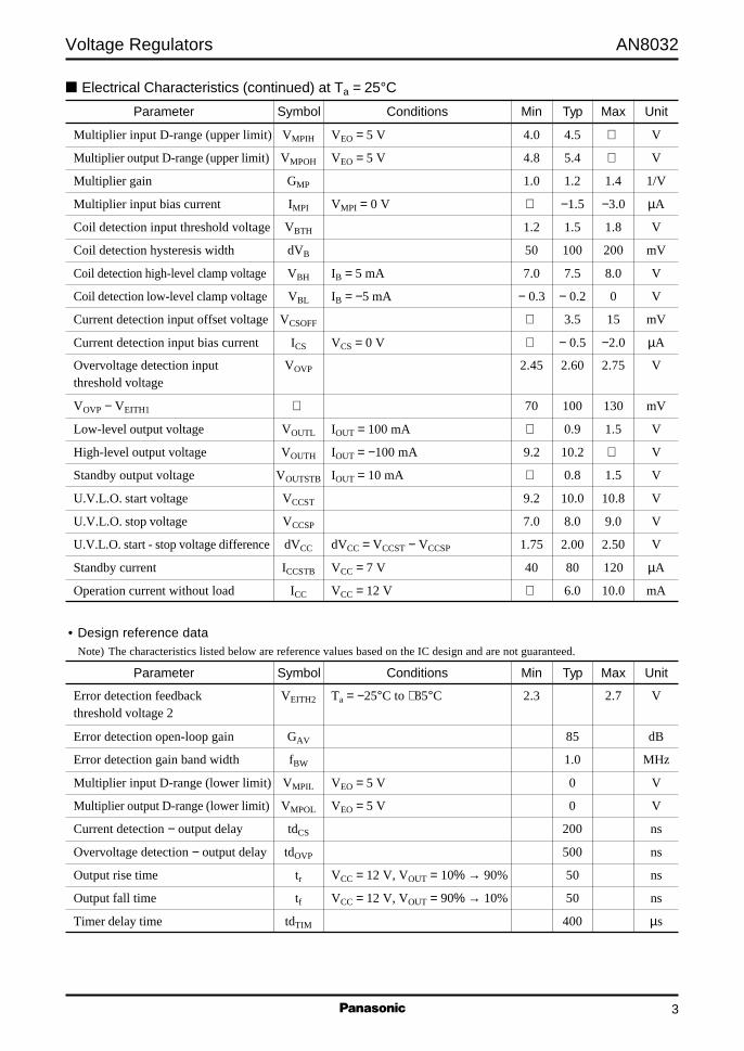
Electrical Characteristics (continued) at Ta = 25°C
Parameter Symbol Conditions Min Typ Max Unit
Multiplier input D-range (upper limit) VMPIH VEO = 5 V 4.0 4.5 V
Multiplier output D-range (upper limit)VMPOH VEO = 5 V 4.8 5.4 V
Multiplier gain GMP 1.0 1.2 1.4 1/V
Multiplier input bias current IMPI VMPI = 0 V −1.5 −3.0 µA
Coil detection input threshold voltage VBTH 1.2 1.5 1.8 V
Coil detection hysteresis width dVB 50 100 200 mV
Coil detection high-level clamp voltage VBH IB = 5 mA 7.0 7.5 8.0 V
Coil detection low-level clamp voltage VBL IB = −5 mA − 0.3 − 0.2 0 V
Current detection input offset voltage VCSOFF 3.5 15 mV
Current detection input bias current ICS VCS = 0 V − 0.5 −2.0 µA
Overvoltage detection input VOVP 2.45 2.60 2.75 Vthreshold voltage
VOVP − VEITH1 70 100 130 mV
Low-level output voltage VOUTL IOUT = 100 mA 0.9 1.5 V
High-level output voltage VOUTH IOUT = −100 mA 9.2 10.2 V
Standby output voltage VOUTSTB IOUT = 10 mA 0.8 1.5 V
U.V.L.O. start voltage VCCST 9.2 10.0 10.8 V
U.V.L.O. stop voltage VCCSP 7.0 8.0 9.0 V
U.V.L.O. start - stop voltage differencedVCC dVCC = VCCST − VCCSP 1.75 2.00 2.50 V
Standby current ICCSTB VCC = 7 V 40 80 120 µA
Operation current without load ICC VCC = 12 V 6.0 10.0 mA
• Design reference dataNote) The characteristics listed below are reference values based on the IC design and are not guaranteed.
Parameter Symbol Conditions Min Typ Max Unit
Error detection feedback VEITH2 Ta = −25°C to +85°C 2.3 2.7 Vthreshold voltage 2
Error detection open-loop gain GAV 85 dB
Error detection gain band width fBW 1.0 MHz
Multiplier input D-range (lower limit) VMPIL VEO = 5 V 0 V
Multiplier output D-range (lower limit) VMPOL VEO = 5 V 0 V
Current detection − output delay tdCS 200 ns
Overvoltage detection − output delay tdOVP 500 ns
Output rise time tr VCC = 12 V, VOUT = 10% → 90% 50 ns
Output fall time tf VCC = 12 V, VOUT = 90% → 10% 50 ns
Timer delay time tdTIM 400 µs
4
AN8032 Voltage Regulators
Terminal Equivalent Circuits
Pin No. Equivalent circuit Description I/O
1 CS: IThe input terminal of comparator which detects
the current value flowing in power MOSFET.
The output level of multiplier and the current value
of power MOSFET input from the CS terminal are
compared. If the later becomes larger than the
former, the VOUT is set to low level and
the power MOSFET ouput is cut.
2 MPI: IThe input terminal of multiplier
The voltage after a full-wave rectified AC input
voltage are monitored.
3 EO: OThe output terminal of error amplifier / the input
terminal of multiplier.
The error amplifier monitors the output voltage
of active filter and amplifies its error portion and
outputs to the multiplier. Therefore, this terminal
serves as another input terminal of the multiplier.
4 EI: IThe inverted input terminal of error amplifier
the overvoltage protection input terminal.
To the noninverted input terminal, the internal
reference voltage of IC (2.5 V typ.) is input.
5 OVP: IOvervoltage detection pin
It is an input terminal with over-voltage detection
function which can detect the overvoltage of the
output voltage to shut off the power MOSFET.
Approx. 7.1 V
1
To high-speedconverter
Approx. 7.1 V
2
Approx. 7.1 V Approx. 7.1 V
3
Error amplifier output Multiplier
input
Approx. 7.1 VApprox. 7.1 V
4Error amplifier input
Approx. 7.1 VApprox. 7.1 V
5Overvoltage protection input
5
Voltage Regulators AN8032
Terminal Equivalent Circuits (continued)
Pin No. Equivalent circuit Description I/O
6 VB: IThe terminal is connected via the transformer's
sub-coil and resistor. The reset of transformer is
detected and the trigger signal to turn on the power
MOSFET is sent.
Since the coil signal of transformer is input as
current, the IC incorporates the circuit which
clamps the upper/lower limit voltage to prevent
malfunction.
7 GND: Grounding terminal
This terminal is used in common for grounding the
control system and the power system.
8 VOUT: OThe output terminal.
It is capable of driving the gate of power MOSFET
directly.
9 VCC: The supply voltage terminal.
The supply voltage terminal for the power system
and that for the signal system are put together as
one terminal with internal connection in order to
greatly decrease the common impedance.
This double-functioning terminal monitors the
supply voltage, and has start/stop operation thresh-
old.
Approx. 7.1 VApprox. 7.1 V
6
Lower limit voltage clamp
Upper limit voltage clamp
VBComparator input
PVCC
7Power system ground
Signal system ground
9
8
VBUpper limit voltage clamp
Power MOSFET drive block
9
Inside bias(Appox. 7.1 V)
U.V.L.O.
6
AN8032 Voltage Regulators
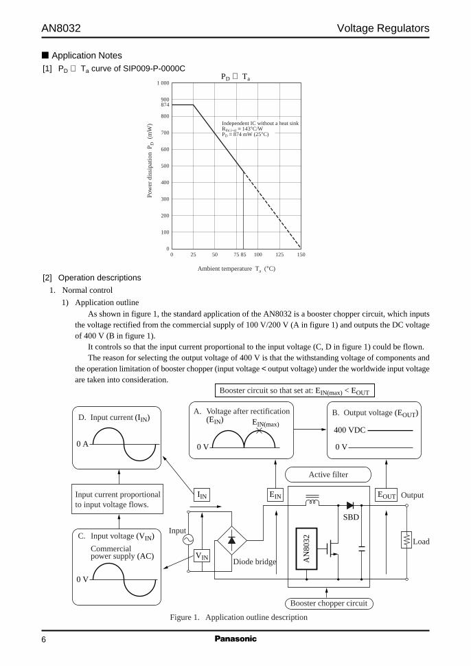
Application Notes[1] PD Ta curve of SIP009-P-0000C
PD Ta
Pow
er d
issi
patio
n P D
(m
W)
00 25 150
Ambient temperature Ta (°C)
50 75 10085 125
100
200
300
400
500
600
700
800
874900
1 000
Independent IC without a heat sinkRth( j−a) = 143°C/WPD = 874 mW (25°C)
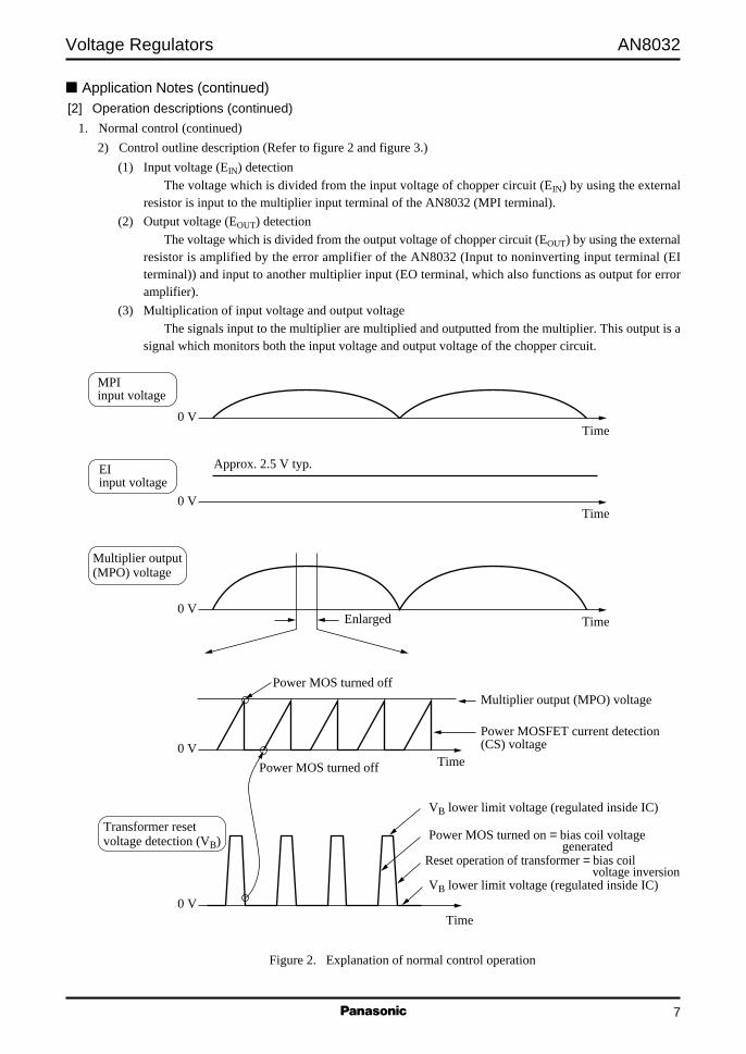
[2] Operation descriptions
1. Normal control
1) Application outlineAs shown in figure 1, the standard application of the AN8032 is a booster chopper circuit, which inputs
the voltage rectified from the commercial supply of 100 V/200 V (A in figure 1) and outputs the DC voltageof 400 V (B in figure 1).
It controls so that the input current proportional to the input voltage (C, D in figure 1) could be flown.The reason for selecting the output voltage of 400 V is that the withstanding voltage of components and
the operation limitation of booster chopper (input voltage < output voltage) under the worldwide input voltageare taken into consideration.
C. Input voltage (VIN)
Commercial power supply (AC)
Figure 1. Application outline description
Input current proportional to input voltage flows.
Booster chopper circuit
Active filter
0 A
D. Input current (IIN)
0 V
0 V
A. Voltage after rectification(EIN) EIN(max)
0 V
B. Output voltage (EOUT)
400 VDC
EOUTEIN
SBD
IIN
VIN Diode bridge AN
8032
Output
Booster circuit so that set at: EIN(max) < EOUT
InputLoad
7
Voltage Regulators AN8032
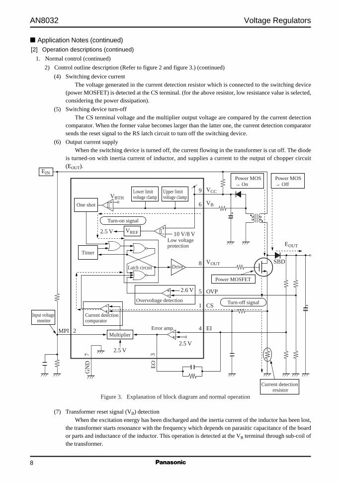
Application Notes (continued)[2] Operation descriptions (continued)
1. Normal control (continued)
2) Control outline description (Refer to figure 2 and figure 3.)
(1) Input voltage (EIN) detectionThe voltage which is divided from the input voltage of chopper circuit (EIN) by using the external
resistor is input to the multiplier input terminal of the AN8032 (MPI terminal).
(2) Output voltage (EOUT) detection
The voltage which is divided from the output voltage of chopper circuit (EOUT) by using the externalresistor is amplified by the error amplifier of the AN8032 (Input to noninverting input terminal (EIterminal)) and input to another multiplier input (EO terminal, which also functions as output for erroramplifier).
(3) Multiplication of input voltage and output voltageThe signals input to the multiplier are multiplied and outputted from the multiplier. This output is a
signal which monitors both the input voltage and output voltage of the chopper circuit.
Figure 2. Explanation of normal control operation
MPI input voltage
EI input voltage
Multiplier output (MPO) voltage
Transformer reset voltage detection (VB)
0 V
0 V
Approx. 2.5 V typ.
0 V
Time
Time
Time
Time0 V
Enlarged
0 VTime
Power MOS turned off
VB lower limit voltage (regulated inside IC)
Power MOS turned on = bias coil voltage generated
Reset operation of transformer = bias coil voltage inversionVB lower limit voltage (regulated inside IC)
Multiplier output (MPO) voltage
Power MOSFET current detection (CS) voltage
Power MOS turned off
8
AN8032 Voltage Regulators
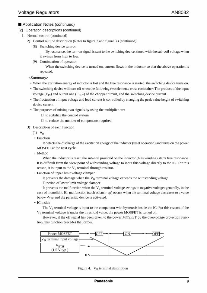
Application Notes (continued)[2] Operation descriptions (continued)
1. Normal control (continued)
2) Control outline description (Refer to figure 2 and figure 3.) (continued)
(4) Switching device currentThe voltage generated in the current detection resistor which is connected to the switching device
(power MOSFET) is detected at the CS terminal. (for the above resistor, low resistance value is selected,considering the power dissipation).
(5) Switching device turn-off
The CS terminal voltage and the multiplier output voltage are compared by the current detectioncomparator. When the former value becomes larger than the latter one, the current detection comparatorsends the reset signal to the RS latch circuit to turn off the switching device.
(6) Output current supplyWhen the switching device is turned off, the current flowing in the transformer is cut off. The diode
is turned-on with inertia current of inductor, and supplies a current to the output of chopper circuit(EOUT).
Lower limit voltage clamp
Input voltage monitor
Upper limit voltage clamp
One shot
Low voltage protection
Latch circuit
Overvoltage detection
Current detection comparator
Error amp.
Timer
Drive
Multiplier
Power MOSFET
Figure 3. Explanation of block diagram and normal operation
Power MOS→ Off
Power MOS→ On
Turn-on signal
Turn-off signal
VCC9
VB
VBTH
VREF 10 V/8 V
2.5 V
2.5 V
2.6 V
6
1
4MPI 2
3
GN
D7
2.5 V
EIN
EO
5
EOUT
SBDVOUT
OVP
CS
EI
8
Current detection resistor
(7) Transformer reset signal (VB) detectionWhen the excitation energy has been discharged and the inertia current of the inductor has been lost,
the transformer starts resonance with the frequency which depends on parasitic capacitance of the boardor parts and inductance of the inductor. This operation is detected at the VB terminal through sub-coil ofthe transformer.
9
Voltage Regulators AN8032
Application Notes (continued)[2] Operation descriptions (continued)
1. Normal control (continued)
2) Control outline description (Refer to figure 2 and figure 3.) (continued)
(8) Switching device turn-onBy resonance, the turn-on signal is sent to the switching device, timed with the sub-coil voltage when
it swings from high to low.
(9) Continuation of operation
When the switching device is turned on, current flows in the inductor so that the above operation isrepeated.
<Summary>
• When the excitation energy of inductor is lost and the free resonance is started, the switching device turns on.
• The switching device will turn off when the following two elements cross each other: The product of the input
voltage (EIN) and output one (EOUT) of the chopper circuit, and the switching device current.
• The fluctuation of input voltage and load current is controlled by changing the peak value height of switchingdevice current.
• The purposes of mixing two signals by using the multiplier are:
to stabilize the control system
to reduce the number of components required
3) Description of each function
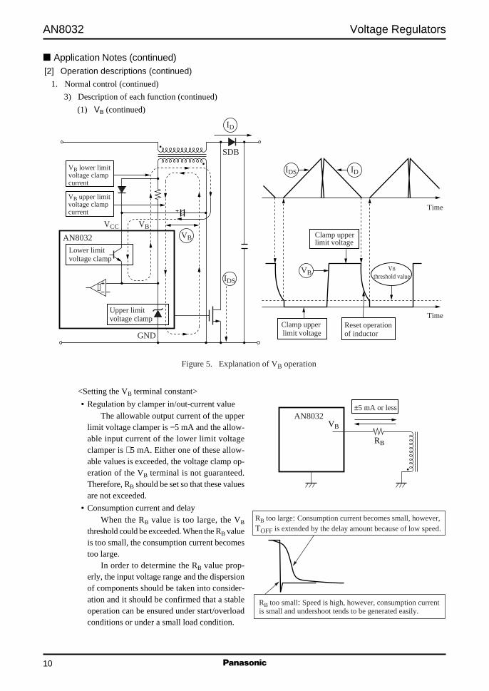
(1) VB
• Function
It detects the discharge of the excitation energy of the inductor (reset operation) and turns on the powerMOSFET at the next cycle.
• MethodWhen the inductor is reset, the sub-coil provided on the inductor (bias winding) starts free resonance.
It is difficult from the view point of withstanding voltage to input this voltage directly to the IC. For thisreason, it is input to the VB terminal through resistor.
• Function of upper limit voltage clamperIt prevents the damage when the VB terminal voltage exceeds the withstanding voltage.Function of lower limit voltage clamperIt prevents the malfunction when the VB terminal voltage swings to negative voltage: generally, in the
case of monolithic IC, malfunction (such as latch-up) occurs when the terminal voltage decreases to a valuebelow -VBE and the parasitic device is activated.
• IC insideThe VB terminal voltage is input to the comparator with hysteresis inside the IC. For this reason, if the
VB terminal voltage is under the threshold value, the power MOSFET is turned on.However, if the off signal has been given to the power MOSFET by the overvoltage protection func-
tion, this function precedes the former.
Figure 4. VB terminal description
0 V
Power MOSFET
VB terminal input voltage
VBTH(1.5 V typ.)
OFF ON OFF
10
AN8032 Voltage Regulators
Application Notes (continued)[2] Operation descriptions (continued)
1. Normal control (continued)
3) Description of each function (continued)
(1) VB (continued)
<Setting the VB terminal constant>
• Regulation by clamper in/out-current valueThe allowable output current of the upper
limit voltage clamper is −5 mA and the allow-able input current of the lower limit voltageclamper is +5 mA. Either one of these allow-able values is exceeded, the voltage clamp op-eration of the VB terminal is not guaranteed.Therefore, RB should be set so that these valuesare not exceeded.
• Consumption current and delayWhen the RB value is too large, the VB
threshold could be exceeded. When the RB valueis too small, the consumption current becomestoo large.
In order to determine the RB value prop-erly, the input voltage range and the dispersionof components should be taken into consider-ation and it should be confirmed that a stableoperation can be ensured under start/overloadconditions or under a small load condition.
ID
SDB
VB lower limit voltage clampcurrent
VB upper limit voltage clampcurrent
Clamp upper limit voltage
Time
Time
Lower limit voltage clamp
Upper limit voltage clamp
VB
VB
threshold value
VBVCC
AN8032
GND
Figure 5. Explanation of VB operation
VB
ID
IDS
IDS
Clamp upperlimit voltage
Reset operation of inductor
AN8032±5 mA or less
VB
RB
RB too large: Consumption current becomes small, however,TOFF is extended by the delay amount because of low speed.
RB too small: Speed is high, however, consumption current is small and undershoot tends to be generated easily.
11
Voltage Regulators AN8032
Application Notes (continued)[2] Operation descriptions (continued)
1. Normal control (continued)
3) Description of each function (continued)
(1) VB (continued)
<Setting the VB terminal constant> (continued)
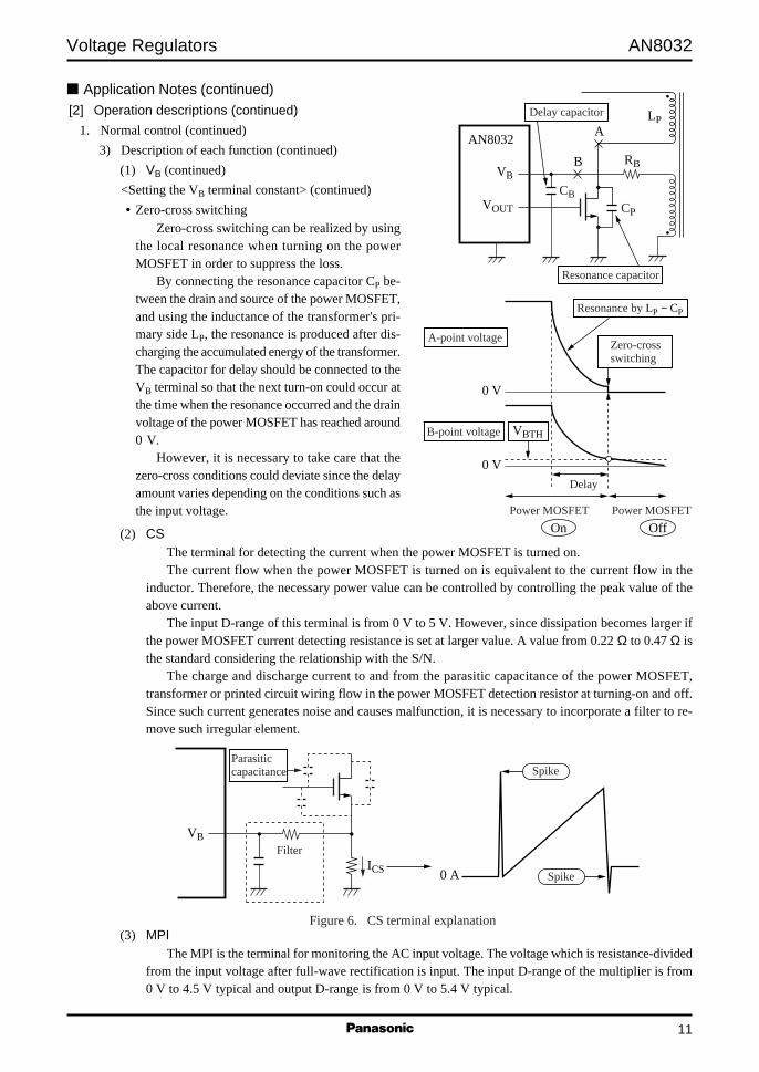
• Zero-cross switchingZero-cross switching can be realized by using
the local resonance when turning on the powerMOSFET in order to suppress the loss.
By connecting the resonance capacitor CP be-tween the drain and source of the power MOSFET,and using the inductance of the transformer's pri-mary side LP, the resonance is produced after dis-charging the accumulated energy of the transformer.The capacitor for delay should be connected to theVB terminal so that the next turn-on could occur atthe time when the resonance occurred and the drainvoltage of the power MOSFET has reached around0 V.
However, it is necessary to take care that thezero-cross conditions could deviate since the delayamount varies depending on the conditions such asthe input voltage.
(2) CSThe terminal for detecting the current when the power MOSFET is turned on.The current flow when the power MOSFET is turned on is equivalent to the current flow in the
inductor. Therefore, the necessary power value can be controlled by controlling the peak value of theabove current.
The input D-range of this terminal is from 0 V to 5 V. However, since dissipation becomes larger ifthe power MOSFET current detecting resistance is set at larger value. A value from 0.22 Ω to 0.47 Ω isthe standard considering the relationship with the S/N.
The charge and discharge current to and from the parasitic capacitance of the power MOSFET,transformer or printed circuit wiring flow in the power MOSFET detection resistor at turning-on and off.Since such current generates noise and causes malfunction, it is necessary to incorporate a filter to re-move such irregular element.
AN8032
Resonance capacitor
Delay capacitor LP
RB
A
B
VOUT
VB
CB
CP
Delay
Power MOSFET Power MOSFET
On Off
Resonance by LP − CP
Zero-cross switching
VBTH
0 V
B-point voltage
0 V
A-point voltage
Figure 6. CS terminal explanation
ICS
VBFilter
Parasitic capacitance Spike
0 A Spike
(3) MPIThe MPI is the terminal for monitoring the AC input voltage. The voltage which is resistance-divided
from the input voltage after full-wave rectification is input. The input D-range of the multiplier is from0 V to 4.5 V typical and output D-range is from 0 V to 5.4 V typical.
12
AN8032 Voltage Regulators
Application Notes (continued)[2] Operation description (continued)
1. Normal control (continued)
3) Description of each function (continued)
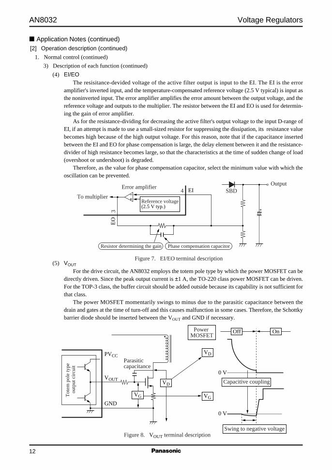
(4) EI/EOThe resisitance-devided voltage of the active filter output is input to the EI. The EI is the error
amplifier's inverted input, and the temperature-compensated reference voltage (2.5 V typical) is input asthe noninverted input. The error amplifier amplifies the error amount between the output voltage, and thereference voltage and outputs to the multiplier. The resistor between the EI and EO is used for determin-ing the gain of error amplifier.
As for the resistance-dividing for decreasing the active filter's output voltage to the input D-range ofEI, if an attempt is made to use a small-sized resistor for suppressing the dissipation, its resistance valuebecomes high because of the high output voltage. For this reason, note that if the capacitance insertedbetween the EI and EO for phase compensation is large, the delay element between it and the resistance-divider of high resistance becomes large, so that the characteristics at the time of sudden change of load(overshoot or undershoot) is degraded.
Therefore, as the value for phase compensation capacitor, select the minimum value with which theoscillation can be prevented.
(5) VOUT
For the drive circuit, the AN8032 employs the totem pole type by which the power MOSFET can bedirectly driven. Since the peak output current is ±1 A, the TO-220 class power MOSFET can be driven.For the TOP-3 class, the buffer circuit should be added outside because its capability is not sufficient forthat class.
The power MOSFET momentarily swings to minus due to the parasitic capacitance between thedrain and gates at the time of turn-off and this causes malfunction in some cases. Therefore, the Schottkybarrier diode should be inserted between the VOUT and GND if necessary.
EO
Reference voltage(2.5 V typ.)
Output
Resistor determining the gain
Error amplifier
To multiplier4
3
EI
Figure 7. EI/EO terminal description
SBD
Phase compensation capacitor
Tot
em p
ole
type
ou
tput
circ
uit
Figure 8. VOUT terminal description
GND
PVCC
Swing to negative voltage
0 V
Parasiticcapacitance
VOUT
Power MOSFET
0 V
Capacitive coupling
VG VG
VD
Off On
VD
13
Voltage Regulators AN8032
Application Notes (continued)[2] Operation descriptions (continued)
1. Normal control (continued)
3) Description of each function (continued)
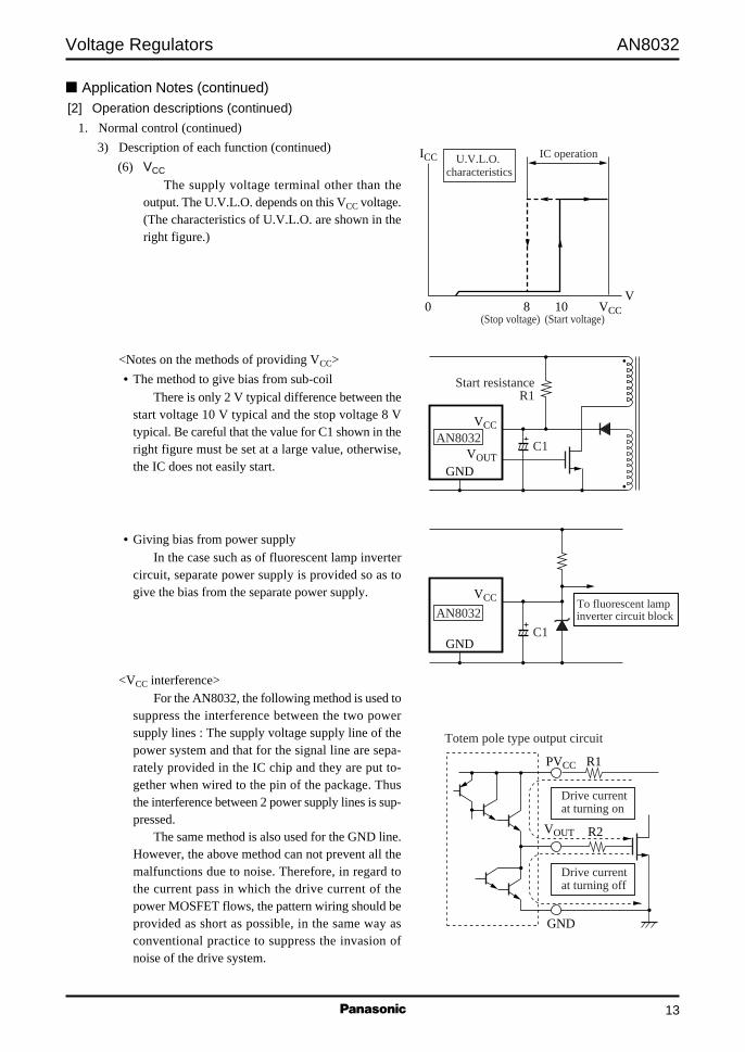
(6) VCC
The supply voltage terminal other than theoutput. The U.V.L.O. depends on this VCC voltage.(The characteristics of U.V.L.O. are shown in theright figure.)
<Notes on the methods of providing VCC>
• The method to give bias from sub-coilThere is only 2 V typical difference between the
start voltage 10 V typical and the stop voltage 8 Vtypical. Be careful that the value for C1 shown in theright figure must be set at a large value, otherwise,the IC does not easily start.
• Giving bias from power supplyIn the case such as of fluorescent lamp inverter
circuit, separate power supply is provided so as togive the bias from the separate power supply.
<VCC interference>For the AN8032, the following method is used to
suppress the interference between the two powersupply lines : The supply voltage supply line of thepower system and that for the signal line are sepa-rately provided in the IC chip and they are put to-gether when wired to the pin of the package. Thusthe interference between 2 power supply lines is sup-pressed.
The same method is also used for the GND line.However, the above method can not prevent all themalfunctions due to noise. Therefore, in regard tothe current pass in which the drive current of thepower MOSFET flows, the pattern wiring should beprovided as short as possible, in the same way asconventional practice to suppress the invasion ofnoise of the drive system.
(Stop voltage) (Start voltage)
ICC
VCCV
0 8 10
IC operationU.V.L.O. characteristics
To fluorescent lamp inverter circuit block
VCC
GNDC1
AN8032
VOUT
Start resistanceR1
VCC
GND
C1AN8032
R2
PVCC
VOUT
GND
R1
Totem pole type output circuit
Drive current at turning on
Drive current at turning off
14
AN8032 Voltage Regulators
Application Notes (continued)[2] Operation descriptions (continued)
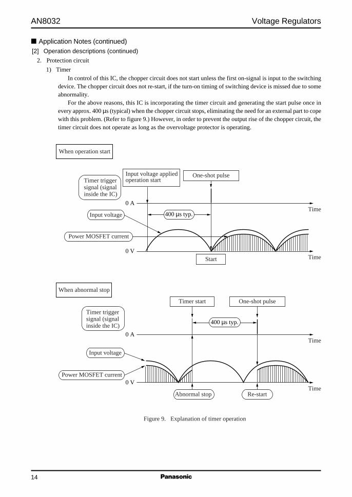
2. Protection circuit
1) Timer
In control of this IC, the chopper circuit does not start unless the first on-signal is input to the switchingdevice. The chopper circuit does not re-start, if the turn-on timing of switching device is missed due to someabnormality.
For the above reasons, this IC is incorporating the timer circuit and generating the start pulse once inevery approx. 400 µs (typical) when the chopper circuit stops, eliminating the need for an external part to copewith this problem. (Refer to figure 9.) However, in order to prevent the output rise of the chopper circuit, thetimer circuit does not operate as long as the overvoltage protector is operating.
Figure 9. Explanation of timer operation
When operation start
0 VTime
0 ATime
400 µs typ.Input voltage
Timer trigger signal (signal inside the IC)
Input voltage applied operation start
Input voltage
Power MOSFET current
When abnormal stop
Timer trigger signal (signal inside the IC)
Abnormal stop
Power MOSFET current
One-shot pulse
Start
0 VTime
0 ATime
400 µs typ.
One-shot pulseTimer start
Re-start
15
Voltage Regulators AN8032
Application Notes (continued)[2] Operation descriptions (continued)
2. Protection circuit (continued)
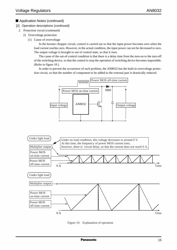
2) Overvoltage protection
(1) Cause of overvoltageIn the booster chopper circuit, control is carried out so that the input power becomes zero when the
load current reaches zero. However, in the actual condition, the input power can not be decreased to zero.The output voltage is brought to out of control state, so that it rises.
The cause of the out-of-control condition is that there is a delay time from the turn-on to the turn-offof the switching device, so that the control to stop the operation of switching device becomes impossible.(Refer to figure 10.)
In order to prevent the occurrence of such problem, the AN8032 has the built-in overvoltage protec-tion circuit, so that the number of component to be added to the external part is drastically reduced.
Under light load
Multiplier output
Power MOS on-time current
Figure 10. Explanation of operation
AN8032Input voltage
Power MOS off-time current
SBDPower MOS on-time current
Output voltage
Time0 A
Time
Power MOS off-time current
Power MOS on-time current
Under light load
Multiplier output
Under no load condition, this voltage decreases to around 0 V. At this time, the frequency of power MOS current rises, however, there is circuit delay, so that the current does not reach 0 A.
0 A
Power MOS off-time current
16
AN8032 Voltage Regulators
Application Notes (continued)[2] Operation descriptions (continued)
2. Protection circuit (continued)
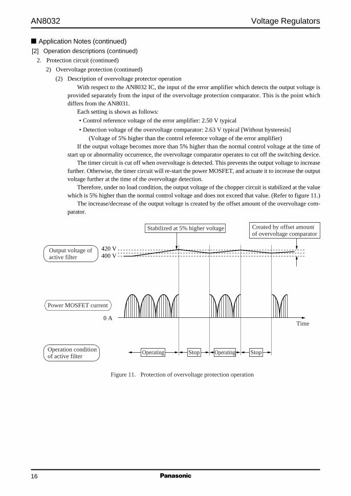
2) Overvoltage protection (continued)
(2) Description of overvoltage protector operationWith respect to the AN8032 IC, the input of the error amplifier which detects the output voltage is
provided separately from the input of the overvoltage protection comparator. This is the point whichdiffers from the AN8031.
Each setting is shown as follows:
• Control reference voltage of the error amplifier: 2.50 V typical
• Detection voltage of the overvoltage comparator: 2.63 V typical [Without hysteresis](Voltage of 5% higher than the control reference voltage of the error amplifier)
If the output voltage becomes more than 5% higher than the normal control voltage at the time ofstart up or abnormality occurrence, the overvoltage comparator operates to cut off the switching device.
The timer circuit is cut off when overvoltage is detected. This prevents the output voltage to increasefurther. Otherwise, the timer circuit will re-start the power MOSFET, and actuate it to increase the outputvoltage further at the time of the overvoltage detection.
Therefore, under no load condition, the output voltage of the chopper circuit is stabilized at the valuewhich is 5% higher than the normal control voltage and does not exceed that value. (Refer to figure 11.)
The increase/decrease of the output voltage is created by the offset amount of the overvoltage com-parator.
Figure 11. Protection of overvoltage protection operation
Stop
Time0 A
420 V400 V
Stabilized at 5% higher voltage Created by offset amount of overvoltage comparator
Output voltage of active filter
Operation condition of active filter
Power MOSFET current
OperatingStopOperating
17
Voltage Regulators AN8032
Application Notes (continued)[2] Operation descriptions (continued)
2. Protection circuit (continued)
2) Overvoltage protection (continued)
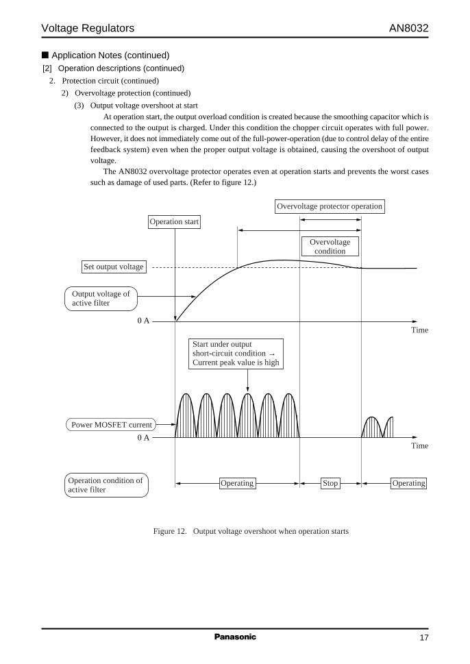
(3) Output voltage overshoot at startAt operation start, the output overload condition is created because the smoothing capacitor which is
connected to the output is charged. Under this condition the chopper circuit operates with full power.However, it does not immediately come out of the full-power-operation (due to control delay of the entirefeedback system) even when the proper output voltage is obtained, causing the overshoot of outputvoltage.
The AN8032 overvoltage protector operates even at operation starts and prevents the worst casessuch as damage of used parts. (Refer to figure 12.)
Figure 12. Output voltage overshoot when operation starts
Time
Time
0 A
Start under outputshort-circuit condition →Current peak value is high
0 A
Stop OperatingOperating
Set output voltage
Overvoltage protector operation
Operation start
Overvoltagecondition
Output voltage of active filter
Operation condition of active filter
Power MOSFET current
18
AN8032 Voltage Regulators
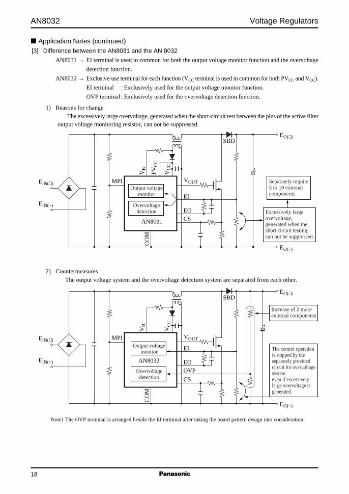
Application Notes (continued)[3] Difference between the AN8031 and the AN 8032
AN8031 → EI terminal is used in common for both the output voltage monitor function and the overvoltage
detection function.
AN8032 → Exclusive-use terminal for each function (VCC terminal is used in common for both PVCC and VCC).
EI terminal : Exclusively used for the output voltage monitor function.
OVP terminal : Exclusively used for the overvoltage detection function.
1) Reasons for changeThe excessively large overvoltage, generated when the short-circuit test between the pins of the active filter
output voltage monitoring resistor, can not be suppressed.
CSEO
EI
VOUT
PV
CC
VC
C
VB
MPI
CO
M
AN8031
EIN(+)
EIN(−)
EO(−)
Output voltagemonitor
Overvoltagedetection Excessively large
overvoltage, generated when the short circuit testing, can not be suppressed.
Separately require 5 to 10 external components
SBDEO(+)
Output voltagemonitor
Overvoltagedetection CS
EOOVP
EI
VOUT
VC
C
VB
MPI
CO
M
AN8032
EIN(+)
EIN(−)
EO(−)
The control operation is stopped by the separately provided circuit for overvoltage system even if excessively large overvoltage is generated.
SBDEO(+)
Increase of 2 more external components
2) CountermeasuresThe output voltage system and the overvoltage detection system are separated from each other.
Note) The OVP terminal is arranged beside the EI terminal after taking the board pattern design into consideration.
19
Voltage Regulators AN8032
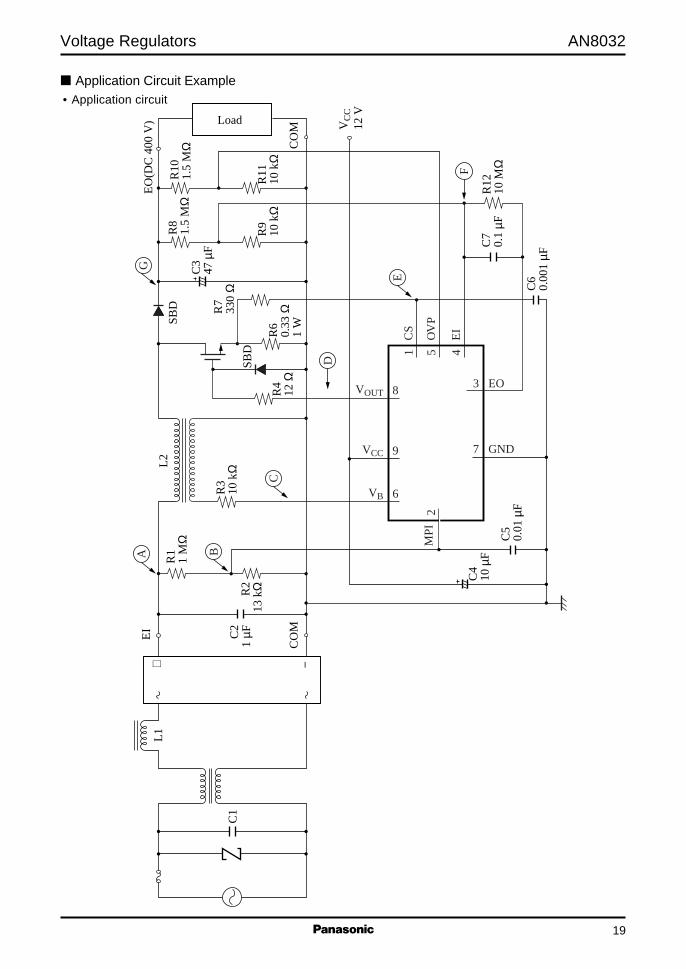
Application Circuit Example• Application circuit
C1
L1E
I
CO
M
C2
1 µF
R2
13 k
Ω
R1
1 M
ΩL2
R3
10 k
Ω
R4
12 Ω
R6
0.33
Ω1
W
R7
330
Ω
C3
47 µ
F C7
0.1
µFR8
1.5
MΩ
R9
10 k
Ω
EO
(DC
400
V)
CO
M
C4
10 µ
F
C5
0.01
µFC
60.
001 µ
F
R12
10 M
Ω
VC
C12
V
SB
D
SB
D+ −
A
D
R10
1.5
MΩ
R11
10 k
Ω
B
C
E
F
G
EI
4
CS
1
OV
P5
MP
I2
VB 6
VCC 9
VOUT 8
GND7
EO3
Load
20
AN8032 Voltage Regulators
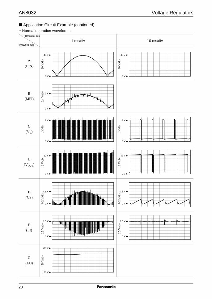
Application Circuit Example (continued)• Normal operation waveforms
Horizontal axis
1 ms/div 10 ms/divMeasuring point
A
(EIN)
B
(MPI)
C
(VB)
D
(VOUT)
E
(CS)
F
(EI)
G
(EO)
1 V
/div
0 V
7 V
2 V
/div
0 V
12 V
0.2
V/d
iv
0 V
0.8 V
0.5
V/d
iv
0 V
2.5 V
50 V
/div
100 V
500 V
0.5
V/d
iv
0 V
2.5 V
0.2
V/d
iv
0 V
0.8 V
2 V
/div
0 V
12 V
1 V
/div
0 V
7 V
0 V
140 V
20 V
/div
0 V
2 V
0.4
V/d
iv
140 V
20 V
/div
0 V
21
Voltage Regulators AN8032
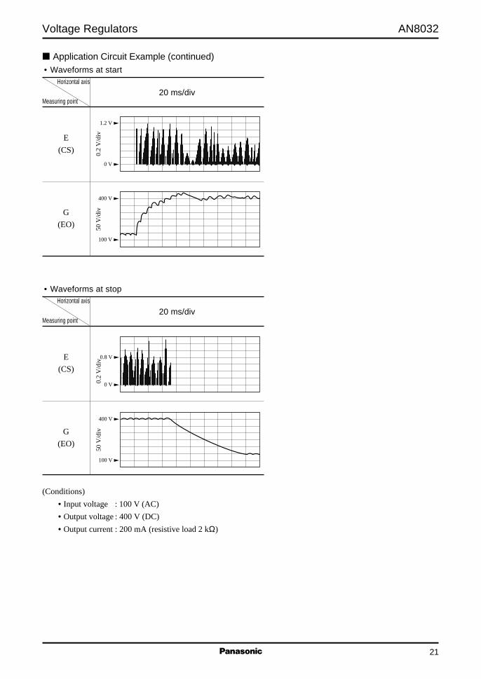
Application Circuit Example (continued)• Waveforms at start
Horizontal axis
20 ms/divMeasuring point
E
(CS)
G
(EO)
• Waveforms at stopHorizontal axis
20 ms/divMeasuring point
E
(CS)
G
(EO)
0.2
V/d
iv
0 V
1.2 V
50 V
/div
100 V
400 V
0.2
V/d
iv
0 V
0.8 V
50 V
/div
100 V
400 V
(Conditions)
• Input voltage : 100 V (AC)
• Output voltage : 400 V (DC)
• Output current : 200 mA (resistive load 2 kΩ)